JP7293389B2 - Storage device and control method - Google Patents
Storage device and control methodDownload PDFInfo
- Publication number
- JP7293389B2 JP7293389B2JP2021555761AJP2021555761AJP7293389B2JP 7293389 B2JP7293389 B2JP 7293389B2JP 2021555761 AJP2021555761 AJP 2021555761AJP 2021555761 AJP2021555761 AJP 2021555761AJP 7293389 B2JP7293389 B2JP 7293389B2
- Authority
- JP
- Japan
- Prior art keywords
- temperature
- storage medium
- stage
- stocker
- storage device
- Prior art date
- Legal status (The legal status is an assumption and is not a legal conclusion. Google has not performed a legal analysis and makes no representation as to the accuracy of the status listed.)
- Active
Links
Images


Classifications
- B—PERFORMING OPERATIONS; TRANSPORTING
- B65—CONVEYING; PACKING; STORING; HANDLING THIN OR FILAMENTARY MATERIAL
- B65G—TRANSPORT OR STORAGE DEVICES, e.g. CONVEYORS FOR LOADING OR TIPPING, SHOP CONVEYOR SYSTEMS OR PNEUMATIC TUBE CONVEYORS
- B65G1/00—Storing articles, individually or in orderly arrangement, in warehouses or magazines
- B65G1/02—Storage devices
- B65G1/04—Storage devices mechanical
- B65G1/137—Storage devices mechanical with arrangements or automatic control means for selecting which articles are to be removed
- B65G1/1373—Storage devices mechanical with arrangements or automatic control means for selecting which articles are to be removed for fulfilling orders in warehouses
- G—PHYSICS
- G01—MEASURING; TESTING
- G01R—MEASURING ELECTRIC VARIABLES; MEASURING MAGNETIC VARIABLES
- G01R1/00—Details of instruments or arrangements of the types included in groups G01R5/00 - G01R13/00 and G01R31/00
- G01R1/02—General constructional details
- G01R1/04—Housings; Supporting members; Arrangements of terminals
- G01R1/0408—Test fixtures or contact fields; Connectors or connecting adaptors; Test clips; Test sockets
- G01R1/0433—Sockets for IC's or transistors
- G01R1/0441—Details
- G01R1/0458—Details related to environmental aspects, e.g. temperature
- G—PHYSICS
- G01—MEASURING; TESTING
- G01R—MEASURING ELECTRIC VARIABLES; MEASURING MAGNETIC VARIABLES
- G01R1/00—Details of instruments or arrangements of the types included in groups G01R5/00 - G01R13/00 and G01R31/00
- G01R1/02—General constructional details
- G01R1/06—Measuring leads; Measuring probes
- G01R1/067—Measuring probes
- G01R1/073—Multiple probes
- G—PHYSICS
- G01—MEASURING; TESTING
- G01R—MEASURING ELECTRIC VARIABLES; MEASURING MAGNETIC VARIABLES
- G01R31/00—Arrangements for testing electric properties; Arrangements for locating electric faults; Arrangements for electrical testing characterised by what is being tested not provided for elsewhere
- G01R31/28—Testing of electronic circuits, e.g. by signal tracer
- G01R31/2851—Testing of integrated circuits [IC]
- G01R31/2855—Environmental, reliability or burn-in testing
- G01R31/286—External aspects, e.g. related to chambers, contacting devices or handlers
- G01R31/2865—Holding devices, e.g. chucks; Handlers or transport devices
- G—PHYSICS
- G01—MEASURING; TESTING
- G01R—MEASURING ELECTRIC VARIABLES; MEASURING MAGNETIC VARIABLES
- G01R31/00—Arrangements for testing electric properties; Arrangements for locating electric faults; Arrangements for electrical testing characterised by what is being tested not provided for elsewhere
- G01R31/28—Testing of electronic circuits, e.g. by signal tracer
- G01R31/2851—Testing of integrated circuits [IC]
- G01R31/2893—Handling, conveying or loading, e.g. belts, boats, vacuum fingers
- H—ELECTRICITY
- H01—ELECTRIC ELEMENTS
- H01L—SEMICONDUCTOR DEVICES NOT COVERED BY CLASS H10
- H01L21/00—Processes or apparatus adapted for the manufacture or treatment of semiconductor or solid state devices or of parts thereof
- H01L21/67—Apparatus specially adapted for handling semiconductor or electric solid state devices during manufacture or treatment thereof; Apparatus specially adapted for handling wafers during manufacture or treatment of semiconductor or electric solid state devices or components ; Apparatus not specifically provided for elsewhere
- H01L21/67005—Apparatus not specifically provided for elsewhere
- H01L21/67011—Apparatus for manufacture or treatment
- H01L21/67098—Apparatus for thermal treatment
- H01L21/67109—Apparatus for thermal treatment mainly by convection
- H—ELECTRICITY
- H01—ELECTRIC ELEMENTS
- H01L—SEMICONDUCTOR DEVICES NOT COVERED BY CLASS H10
- H01L21/00—Processes or apparatus adapted for the manufacture or treatment of semiconductor or solid state devices or of parts thereof
- H01L21/67—Apparatus specially adapted for handling semiconductor or electric solid state devices during manufacture or treatment thereof; Apparatus specially adapted for handling wafers during manufacture or treatment of semiconductor or electric solid state devices or components ; Apparatus not specifically provided for elsewhere
- H01L21/67005—Apparatus not specifically provided for elsewhere
- H01L21/67242—Apparatus for monitoring, sorting or marking
- H01L21/67248—Temperature monitoring
- G—PHYSICS
- G11—INFORMATION STORAGE
- G11C—STATIC STORES
- G11C29/00—Checking stores for correct operation ; Subsequent repair; Testing stores during standby or offline operation
- G11C29/04—Detection or location of defective memory elements, e.g. cell constructio details, timing of test signals
- G11C2029/0403—Detection or location of defective memory elements, e.g. cell constructio details, timing of test signals during or with feedback to manufacture
- G—PHYSICS
- G11—INFORMATION STORAGE
- G11C—STATIC STORES
- G11C7/00—Arrangements for writing information into, or reading information out from, a digital store
- G11C7/04—Arrangements for writing information into, or reading information out from, a digital store with means for avoiding disturbances due to temperature effects
Landscapes
- Engineering & Computer Science (AREA)
- General Physics & Mathematics (AREA)
- Physics & Mathematics (AREA)
- Computer Hardware Design (AREA)
- Microelectronics & Electronic Packaging (AREA)
- Manufacturing & Machinery (AREA)
- Condensed Matter Physics & Semiconductors (AREA)
- General Engineering & Computer Science (AREA)
- Power Engineering (AREA)
- Mechanical Engineering (AREA)
- Environmental & Geological Engineering (AREA)
- Testing Or Measuring Of Semiconductors Or The Like (AREA)
- Container, Conveyance, Adherence, Positioning, Of Wafer (AREA)
- Test And Diagnosis Of Digital Computers (AREA)
- Testing Of Individual Semiconductor Devices (AREA)
- Control Of Temperature (AREA)
Description
Translated fromJapanese本発明の実施形態は、ストレージデバイスおよび制御方法に関する。 Embodiments of the present invention relate to storage devices and control methods.
近年、SSD(solid state drive)やHDD(hard disk drive)など、様々なストレージデバイスが利用されている。たとえばSSDに搭載されるNAND型フラッシュメモリは、半導体ウェハ上に半導体チップとして複数形成された後、ダイシングを行うことによって製造されている。 In recent years, various storage devices such as SSDs (solid state drives) and HDDs (hard disk drives) have been used. For example, a NAND flash memory mounted on an SSD is manufactured by dicing after forming a plurality of semiconductor chips on a semiconductor wafer.
また、半導体チップが形成された半導体ウェハと、半導体チップを検査する検査装置との間で電気信号を中継する検査治具として、プローブカードが利用されている。プローブカードは、簡略化していえば、プリント基板PCBとプローブとで構成される。プローバーは、半導体ウェハに形成されているパッド電極とプローブカードのプローブとを接触させて、たとえばプリント基板PCB上のデバイスと半導体ウェハとを電気的に接続させる。 Further, a probe card is used as an inspection jig that relays electrical signals between a semiconductor wafer on which semiconductor chips are formed and an inspection apparatus that inspects the semiconductor chips. A probe card is simply composed of a printed circuit board PCB and probes. The prober brings the pad electrodes formed on the semiconductor wafer into contact with the probes of the probe card to electrically connect the devices on the printed circuit board PCB and the semiconductor wafer, for example.
実施形態の一つは、複数の不揮発性メモリチップを含む半導体ウェハに関する様々な温度制御を適切に行うことができるストレージデバイスおよび制御方法を提供する。 One of the embodiments provides a storage device and control method capable of appropriately performing various temperature controls on a semiconductor wafer including multiple nonvolatile memory chips.
実施形態によれば、ストレージデバイスは、制御装置とストッカーとを具備する。前記制御装置は、複数のNAND型フラッシュメモリチップを含むストレージ媒体へデータを書き込み、または、前記ストレージ媒体からデータを読み出す。前記ストッカーは、前記制御装置から抜脱されている状態にある複数の前記ストレージ媒体を格納する。前記制御装置は、第1温度制御機構を有する。前記第1温度制御機構は、前記ストレージ媒体を第1温度以上に昇温する。前記ストッカーは、第2温度制御機構を有する。前記第2温度制御機構は、前記ストレージ媒体を前記第1温度より低い第2温度以下に冷却する。According to embodiments, a storage device comprises a controller and a stocker. The control device writes data to or reads data from a storage medium including a plurality ofNAND flash memory chips. The stocker stores a plurality of storage media that are removed from the control device. The controller has a first temperature control mechanism. The first temperature control mechanism raises the temperature of the storage medium to a first temperature or higher. The stocker has a second temperature control mechanism. The second temperature control mechanism cools the storage medium to a second temperature lower than the first temperature.
以下、実施の形態について、図面を参照して説明する。 Embodiments will be described below with reference to the drawings.
図1は、本実施形態のストレージデバイス1の一構成例を示す図である。 FIG. 1 is a diagram showing a configuration example of a
本実施形態では、検査治具であるプローブカードを転用して、ダイシングをせずに半導体ウェハ単位で大容量のストレージデバイス1を構築することを想定する。さらには、プローブと電気的に接続される半導体ウェハを入れ替え可能として、複数の半導体ウェハを搭載することで、より大容量のストレージデバイス1を構築することを想定する。 In this embodiment, it is assumed that a probe card, which is an inspection jig, is diverted to construct a large-
このようなストレージデバイス1を構築するにあたっては、プローバー内の半導体ウェハは常温以上の高温かつ半導体ウェハ内で温度を均一に保つことが好ましく、一方、ブローバー外で保管される半導体ウェハは常温以下の低温に保つことが好ましい。 In constructing such a
ストレージデバイス1は、リーダー&ライター(プローバー)100と、ストレージ搬送システム200と、ストッカー300とを有する。図1では、プローバー100が2つ設けられている例を示しているが、これに限らず、プローバー100の数は、様々に変更し得る。また、ストレージデバイス1は、プローバー100内、ストレージ搬送システム200内、ストッカー300内の気相雰囲気を、水を含まない乾燥空気、希ガス、不活性ガスなどに置換するための空調制御機構500を有する。 The
ストレージデバイス1は、複数のNAND型フラッシュメモリチップ(NANDチップ)が形成された半導体ウェハ(ウェハ400)をストレージとして搭載する。また、ストレージデバイス1は、複数のウェハ400を搭載し、当該複数のウェハ400の中から所定数のウェハ400(図1の例の場合、2つのウェハ400)を適宜に選択して使用する。具体的には、ストレージデバイス1は、プローバー100内のウェハ400を、ストッカー300内のウェハ400と入れ替えることができる。 The
プローバー100は、プローブカード110と、ステージ120と、駆動部130とを有する。 The
プローブカード110は、ステージ120上のウェハ400と電気的に接続するユニットである。前述したように、プローブカード110は、簡略化していえば、プリント基板PCBとプローブとで構成される。本実施形態のストレージデバイス1では、ウェハ400に形成されたNANDチップへのデータの書き込みや、NANDチップからのデータの読み出しを制御するコントローラーなどが、プローブカード110のプリント基板PCB上にデバイス111として配置される。また、本実施形態のストレージデバイス1では、プローブカード110内に、温度制御機構(加熱冷却機構112、冷却機構113、断熱材114)が設けられる。プローブカード110内に設けられる温度制御機構については後述する。 The
ステージ120は、ウェハ400を保持するユニットである。本実施形態のストレージデバイス1では、ステージ120内にも、温度制御機構(加熱冷却機構121)が設けられる。ステージ120内に設けられる温度制御機構についても後述する。 A
駆動部130は、ステージ120を移動させて、ウェハ400上に形成されたパッド電極にプローブカード110のプローブを接触させるユニットである。ここでは、駆動部130は、ステージ120を移動させることを想定するが、プローブカード110を移動させるものであってもよい。また、駆動部130は、プローブカード110とステージ120との両方を移動させるものであってもよい。駆動部130は、パッド電極に接触しているプローブをパッド電極から引き離すようにステージ120を移動させることもできる。 The
図2に、駆動部130によって、ウェハ400上に形成されているパッド電極410にプローブカード110のプローブ115が接触している状態を示す。 FIG. 2 shows a state in which the
パッド電極410にプローブ115が接触すると、プローブカード110のプリント基板PCB上にデバイス111の1つとして配置されるコントローラーが、ウェハ400に形成されているNANDチップと電気的に接続される。これによって、コントローラーは、NANDチップへのデータの書き込みや、NANDチップからのデータの読み出し、NANDチップ内のデータの消去を制御することができる。 When the
図1に戻り、ストレージデバイス1の一構成例についての説明を続ける。 Returning to FIG. 1, the description of the configuration example of the
ストレージ搬送システム200は、ストレージ搬送機210を有する。 The
ストレージ搬送機210は、本実施形態のストレージデバイス1におけるストレージであるウェハ400を、ストッカー300からプローバー100へ、または、プローバー100からストッカー300へ搬送する。なお、以下に説明する構成は一例であり、ウェハ400を搬送する手段はこれに限らない。ストレージ搬送機210は、鉛直方向および水平方向に移動可能である。ストレージ搬送機210は、鉛直方向を軸として回動可能である支持体211と、たとえば細長い板状の形状を有しており、長手方向の一端を水平方向へ突出させるように他端が支持体211に支持されるトレイ212とで構成される。ストッカー300内のウェハ400を入れ替える場合、ストレージ搬送機210は、第1に、プローバー100からストッカー300へウェハ400を搬送するための動作を行う。具体的には、(1)トレイ212の高さがプローバー100内のウェハ400を取り出すために好適な高さとなるように鉛直方向に移動、(2)トレイ212がプローバー100側へ向くように回動、(3)プローバー100内のウェハ400をトレイ212に保持させるためにプローバー100側へ水平方向に移動、(4)ウェハ400をプローバー100内から取り外すためにプローバー100の反対側へ水平方向に移動、(5)トレイ212がストッカー300側へ向くように回動、(6)トレイ212の高さがストッカー300内へウェハ400を収納するために好適な高さとなるように鉛直方向に移動、(7)ウェハ400をストッカー300内へ収納するためにストッカー300側へ水平方向に移動、(8)トレイ212をストッカー300から抜き取るためにストッカー300の反対側へ水平方向に移動、などといった手順で動作する。この手順は単なる一例であって、(1)と(2)の順序を逆転させたり、(6)と(7)の順序を逆転させたりなど、様々に変更し得る。 The
続いて、ストレージ搬送機210は、第2に、ストッカー300からプローバー100へウェハ400を搬送するための動作を行う。この手順は、プローバー100からストッカー300へウェハ400を搬送するための動作と類似するので、その説明については省略する。 Subsequently, the
ストッカー300は、プローバー100から取り外された状態の複数のウェハ400を保管する。本実施形態のストレージデバイス1では、ストッカー300内にも、温度制御機構(冷却機構310)が設けられる。ストッカー300内に設けられる当該温度制御機構については後述する。
空調制御機構500は、空間を外気から分離し、排気ファンで外部から吸気することによって減圧化された空間内に、水を含まない乾燥空気、希ガス、不活性ガスなどを流入することで、空間内を乾燥空気、希ガス、不活性ガスなどに置換する構造を有する。空調制御機構500によって、プローバー100内、ストレージ搬送システム200内、ストッカー300内の気相雰囲気を、水を含まない乾燥空気、希ガス、不活性ガスなどに置換する理由については後述する。 The air
図3は、図1を参照して説明したプローバー100、ストレージ搬送システム200およびストッカー300によって構成されるストレージデバイス1を模式的に示すブロック図である。 FIG. 3 is a block diagram schematically showing the
前述したように、本実施形態のストレージデバイス1では、ウェハ400に形成されたNANDチップへのデータの書き込みや、NANDチップからのデータの読み出しを制御するコントローラー111-1が、プローブカード110のプリント基板PCB上にデバイス111の1つとして配置される。コントローラー111-1は複数配置され得る。つまり、ウェハ400上のすべてのNANDチップを1つのコントローラー111-1で制御してもよいし、複数のコントローラー111-1で制御してもよい。図3では、書き込みデータや読み出しデータを一時的に格納するためのバッファメモリ111-2が、コントローラー111-1と同様、プローブカード110のプリント基板PCB上にデバイス111の1つとして配置される例を示している。バッファメモリ111-2は、コントローラー111-1に内蔵されるものであってもよい。 As described above, in the
コントローラー111-1は、プローブカード110のプローブ115がステージ120上のウェハ400のパッド電極410と接触することで、ウェハ400のNANDチップと電気的に接続される。コントローラー111-1は、ホスト2からの要求に応じて、NANDチップへのデータの書き込みや、NANDチップからのデータの読み出しを制御することが可能となる。また、プローバー100内のウェハ400は、ストレージ搬送システム200により、ストッカー300で保管されているウェハ400と入れ替えることができる。 The controller 111 - 1 is electrically connected to the NAND chips of the
また、ストレージデバイス1は、制御部10を有する。制御部10は、たとえば空調制御系11、温度制御系12、駆動制御系13、インターフェース制御系14を含み、ストレージデバイス1の動作全体を制御する。制御部10の各制御系は、たとえばプロセッサがファームウェアを実行することにより実現される。空調制御系11は、空調制御機構500を制御する。温度制御系12は、プローブカード110内の温度制御機構(加熱冷却機構112、冷却機構113)、ステージ120内の温度制御機構(加熱冷却機構121)、ストッカー300内の温度制御機構(冷却機構310)を統合的に制御する。駆動制御系13は、駆動部130、ストレージ搬送機210を制御する。インターフェース制御系14は、ホスト2とプローブカード11との間の通信を制御する。また、インターフェース制御系14は、当該通信の制御結果に基づき、空調制御系11、温度制御系12、駆動制御系13を制御する。 The
ウェハ400のNANDチップへのデータの書き込みや、NANDチップからのデータの読み出しは、常温以上の高温(例えば75℃、ただし例えば85℃以下)で実施することが好ましい。より詳しくは、NANDチップ内のセルにデータを書き込み読み出す際には、高温にするほどセルの電荷蓄積層に電子がトラップされる準位が深く安定化するため、1電子あたりのノイズのばらつきが減る。よって、高温であることが好ましい。一方、NANDチップ上でのデータの長期保存には、常温以下の低温(例えば0℃以下)であることが好ましい。より詳しくは、NANDチップに蓄えられた電荷のフォノン散乱を抑制することで電荷保持時間を長くすることができる。よってウェハ400を保管する際の温度は低温が好ましい。また、プローブカード110上に実装されるデバイス111は、閾値以下の温度で動作させることが好ましい。このように、ウェハ400をストレージとして用いる場合、ストレージデバイス1内において様々な温度制御が求められる。そこで、本実施形態のストレージデバイス1は、プローバー100、ストレージ搬送システム200およびストッカー300に各々温度制御機構を設け、ストレージデバイス1全体として適切な温度制御を行うようにしたものである。以下、この点について詳述する。 Writing data to the NAND chips of the
まず、プローバー100に設けられる温度制御機構について説明する。 First, the temperature control mechanism provided in the
前述したように、プローバー100においては、プローブカード110内と、ステージ120内とに温度制御機構が設けられる。 As described above, in the
ウェハ400を保持するステージ120内には、ステージ120上でプローブカード110と電気的に接続されたウェハ400内を極力同一の温度とするための加熱冷却機構121が設けられる(図1参照)。加熱冷却機構121は、たとえば電気加熱および冷却管を用いた温度制御機構である。ステージ120によるウェハ400の温度制御のために、ストレージデバイス1では、ウェハ400より面積の小さい複数の異なる領域ごと、たとえばウェハ400内のNANDチップ領域ごとに、温度制御領域を設定し、それぞれで異なる温度制御を行えるようにしている。 A heating and
図4は、本実施形態のストレージデバイス1におけるステージ120に関する温度制御領域の一設定例を説明するための図である。 FIG. 4 is a diagram for explaining a setting example of the temperature control area for the
図4(A)は、ウェハ400の上面を示し、かつ、ウェハ400内でのNANDチップ420の一形成例を示している。一方、図4(B)は、ステージ120のウェハ400を保持する上面を示し、かつ、ステージ120に関する温度制御領域a1の一設定例を示している。 FIG. 4A shows the top surface of the
図4に示すように、本実施形態のストレージデバイス1においては、たとえば、ステージ120上に置かれたウェハ400上に形成されている複数のNANDチップ420と一対一で位置的に対応するように、複数の温度制御領域a1がステージ120上に設定される。複数の温度制御領域a1は、たとえば、2以上のNANDチップ420に対して1つが位置的に対応するように設定することも可能である。また、温度制御領域a1が対応づけられるNANDチップ420の数は、すべての温度制御領域a1で同一となっていなくともよい。 As shown in FIG. 4, in the
図5は、たとえば図4に示すように設定される温度制御領域a1ごとに温度制御を行うためにステージ120内に設けられる加熱冷却機構121の一構成例を示す図である。 FIG. 5 is a diagram showing one configuration example of the heating/
加熱冷却機構121の冷却機構は、たとえば、2本の冷却管1211の一方から他方へ冷却支管1212経由で冷媒b1を流通させる構造を有する。冷媒b1は、電子冷却によって冷却された水や液体窒素などである。冷却支管1212は、ステージ120上に設定された温度制御領域a1ごとにステージ120上のウェハ400を冷却できるように配置される。冷却支管1212による冷却は、冷媒b1の流入量によって制御される。冷媒b1の流入量を制御するために、冷却支管1212のたとえば注入口近傍には、電子制御型モーターバルブ1213と、流量計1214とが設置されている。 The cooling mechanism of the heating/
一方、加熱冷却機構121の加熱機構は、たとえば、ステージ120上に設定された温度制御領域a1ごとにステージ120上のウェハ400を加熱できるように配置されるヒーター線1215を用いて構成される。ヒーター線1215による加熱は、たとえば、加熱有無を切り替えるためのスイッチと、発熱量を調整するための可変抵抗とによって制御することができる。 On the other hand, the heating mechanism of the heating/
なお、詳細については後述するが、このように構成されるステージ120の加熱冷却機構121は、たとえば、プローブカード110上に配置されるコントローラー111-1によって制御される。ステージ120内には、たとえばI2Cバスに温度データを出力することができる温度計が設けられている。また、ウェハ400内にも、温度計が設けられてもよい。Although the details will be described later, the heating and
プローブカード110とステージ120との間には、ステージ120内またはウェハ400内に設けられる温度計が計測した温度をコントローラー111-1へ転送可能な通信路が設けられている。制御部10と連携して、コントローラー111-1は、ステージ120内またはウェハ400内に設けられる温度計が計測した温度に基づき、ステージ120の加熱冷却機構121を制御する。複数のコントローラー111-1が存在する場合、それらの中の1つが加熱冷却機構121の制御を担ってもよいし、複数のコントローラー111-1が協働して、加熱冷却機構121の制御を実施してもよい。後述する、プローブカード110内に設けられる温度制御機構(加熱冷却機構112、冷却機構113)の制御も、コントローラー111-1によって実行される。つまり、プローバー100内の温度制御機構は、コントローラー111-1によって一元的に制御される。プローバー100内の温度制御機構を一元的に制御するためのデバイスを、コントローラー111-1とは別に用意して、プローブカード110上に配置することも可能である。または、コントローラー111-1以外の既存のデバイスに、プローバー100内の温度制御機構を一元的に制御するための機能を搭載してもよい。 A communication path is provided between the
また、図5には、駆動部130のリフトピン131とアクチュエータ132とが併せて示されている。リフトピン131は、ステージ120に設けられる孔部に嵌め込まれ、ステージ120を鉛直方向または水平方向へ移動させるための部材である。アクチュエータ132は、リフトピン131を鉛直方向または水平方向へ移動させることにより、ステージ120を鉛直方向または水平方向へ移動させることができる。水平方向の移動は、ウェハ400のパッド電極410と、プローブカード110のプローブ115との位置を合わせるために行われる。一方、鉛直方向の移動は、ウェハ400のパッド電極410と、プローブカード110のプローブ115とを接触させるため、または、接触している状態のパッド電極410とプローブ115とを引き離すために行われる。 FIG. 5 also shows lift pins 131 and
図6は、たとえば図5に示すように構成される加熱冷却機構121のステージ120内における一配置例を示す図である。 FIG. 6 is a diagram showing an arrangement example in the
図6(A)は、ウェハ400の上面を示し、かつ、ウェハ400内でのNANDチップ420の一形成例を示している。一方、図6(B)は、ステージ120のウェハ400を保持する上面を示し、かつ、ステージ120内における加熱冷却機構121の一配置例を示している。 FIG. 6A shows the top surface of the
図5を参照して説明した、加熱冷却機構121が備える冷却用の冷却支管1212や加熱用のヒーター線1215は、図6(B)に示すように、必ずしも、すべての温度制御領域a1を経由するように配置しなくともよい。たとえば近傍の1以上の冷却支管1212や1以上のヒーター線1215を用いて目的の温度制御領域a1の温度を制御することも可能である。 The cooling
図7は、ステージ120に設けられる加熱冷却機構121による温度制御の一例を説明するための図である。 FIG. 7 is a diagram for explaining an example of temperature control by the heating/
図7(A)は、ステージ120上のウェハ400内の温度が不均一になっている場合の一例を示している。具体的には、ウェハ400が、中央部の温度が高く、中央部から端部へ温度が低くなっている状態を示している。 FIG. 7A shows an example where the temperature inside the
一方、図7(B)は、ウェハ400が図7(A)に示す状態となっている場合に実施される加熱冷却機構121による温度制御の一例を示している。 On the other hand, FIG. 7B shows an example of temperature control by the heating/
この場合、温度の均一化のために、ウェハ400の中心部については、中央部に配置されている冷却支管1212に冷媒b1を流す冷却が行われ、ウェハ400の端部については、端部に配置されているヒーター線1215を発熱させる加熱が行われる。その際、冷却支管1212への冷媒b1の流量は、中心に近い程大きく、中心から離れる程小さくなるように制御され、逆に、ヒーター線1215の発熱量は、中心に近い程小さく、中心から離れる程大きくなるように制御される。 In this case, in order to make the temperature uniform, the central portion of the
このように、ステージ120に加熱冷却機構121を設ける本実施形態のストレージデバイス1においては、ステージ120上のウェハ400内の温度が均一になるように制御することができる。なお、図7では、説明をわかり易くするために、ウェハ400の中央部の温度が上昇してウェハ400内の温度が不均一化している状態を示したが、ウェハ400内の温度の不均一化は、NANDチップ420へのアクセス状況などによって、様々な状態で現れ得る。温度の不均一化がどのような状態で現れても、ステージ120上に複数の温度制御領域a1を設定する本実施形態のストレージデバイス1においては、ウェハ400内の温度の均一化を適切に実施することができる。 Thus, in the
また、ストッカー300の冷却機構310については後述するが、ストッカー300に保管されているウェハ400は、データの長期保存に適した常温以下の低温に冷却されている。これに対して、NANDチップ420へのデータの書き込みやNANDチップ420からのデータの読み出しは、常温以上の高温で実施されることが好ましい。ステージ120に加熱冷却機構121を設ける本実施形態のストレージデバイス1においては、プローバー100内のウェハ400の入れ替え時、ストッカー300から搬送されてきた低温のウェハ400を、プローブカード110と電気的に接続する前に、NANDチップ420へのデータの書き込みやNANDチップ420からのデータの読み出しに適した温度まで昇温することができる。また、接触時におけるプローブカード110のプローブ150およびウェハ400のパッド電極410の双方にダメージを与えることを防止できる。 Also, although the
さらに、ステージ120に加熱冷却機構121を設ける本実施形態のストレージデバイス1においては、逆に、プローバー100内のウェハ400の入れ替え時、常温以上に維持されていたステージ120上のウェハ400を、プローブカード110から電気的に切断した後、ストッカー300へ搬送する前に、ステージ120上でたとえは常温以下に冷却することも可能である。ステージ120上で冷却したウェハ400をストッカー300に格納することで、ストッカー300内の温度が一時的ではあっても上昇し、ストッカー300内の他のウェハ400へ影響を及ぼすことを防止できる。また、プローバー100とストッカー300との間に介在するストレージ搬送システム200内に、プローバー100のステージ120上において常温以上に維持されていたウェハ400を常温以下に冷却するための冷却機構を設けてもよい。 Furthermore, in the
プローブカード110内の温度制御機構としては、加熱冷却機構112と、冷却機構113と、断熱材114とが設けられる(図1参照)。 A heating/
加熱冷却機構112は、たとえば、ステージ120の加熱冷却機構121と同様の電気加熱および冷却管を用いた温度制御機構である。ステージ120の加熱冷却機構121と同様でもよいので、その構成の説明については省略する。ステージ120の加熱冷却機構121と異なる構成としても構わない。 The heating/
加熱冷却機構112は、プローブカード110の温度をウェハ400の温度とほぼ一致させるために、より詳しくは、プローブ115の温度をパッド電極410の温度とほぼ一致させるために、ステージ120上のウェハ400と対向するプローブカード110内のたとえば下面側に設けられる。 The heating/
これにより、本実施形態のストレージデバイス1は、パッド電極410へプローブ115を接触させることによるウェハ400とプローブカード110との電気的な接続の安定化を図ることなどが可能となる。 As a result, the
また、プローブカード110の冷却機構113は、たとえば、放熱または冷却管を用いた温度制御機構である。冷却機構113は、プローブカード110のプリント基板PCB上に配置されるデバイス111を閾値以下の温度で動作させるため、換言すれば、デバイス111の温度が閾値を超えないようにするために、プローブカード110内のたとえば上面側に設けられる。冷却機構113の制御は、デバイス111の1つであるコントローラー111-1によって実行される。コントローラー111-1は、自身が計測したコントローラー111-1の温度と、プリント基板PCB上の他のデバイスが計測した温度とに基づき、冷却機構113を制御する。冷却機構113も、加熱冷却機構112や、ステージ120の加熱冷却機構121と同様、あらかじめ設定した温度制御領域ごとに温度制御を行うことができる。この温度制御領域は、ステージ120上において設定される温度制御領域a1と対応するものであってもよいし、独自に設定されるものであってもよい。 Also, the
これにより、本実施形態のストレージデバイス1は、プローブカード110に配置されるデバイス111を適切な環境下で動作させ続けることが可能となる。 As a result, the
また、プローブカード110には、デバイス111が配置されるたとえば上面と、ウェハ400と対向するたとえば下面との間に、熱抵抗の高い断熱材114が設けられる。断熱材114を設けることで、本実施形態のストレージデバイス1は、プローブカード110内を上面側と下面側とで断熱し、各々異なる温度を維持することを可能とする。より詳しくは、たとえば上面側は、デバイス111に適した温度に維持し、たとえば下面側は、ステージ120上のウェハ400の温度とほぼ一致する温度に維持することができる。 Further, the
図8は、ストレージデバイス1においてプローブカード110上のデバイス111(コントローラー111-1)がプローバー100の温度制御を一元的に実施する仕組みの一例を説明するための図である。 FIG. 8 is a diagram for explaining an example of a mechanism in which the device 111 (controller 111-1) on the
プローブカード110には、放熱効果の高いセラミックプリント基板PCB1101が設けられている。このセラミックプリント基板PCB1101のたとえば上面に配置される複数のデバイス111のいくつかは、デバイス111の温度を計測する温度計1111を備える。コントローラー111-1も、温度計1111を備えている。コントローラー111-1は、第1に、自身が備える温度計1111を含む、これらの温度計1111によって計測された温度に基づき、デバイス111の温度を閾値以下に保つように、冷却機構113による温度制御を実行する。前述したように、コントローラー111-1は、冷却機構113による温度制御を、あらかじめ設定される温度制御領域ごとに実行することができる。なお、デバイス111の温度を計測する温度計1111は、デバイス111外であっても良い。 The
セラミックプリント基板PCB1101のたとえば下面には、インターポーザー1102を介してプローブユニット1103が配置される。プローブ115は、プローブユニット1103の先端部に設けられている。また、この下面側には、たとえばコントローラー111-1に温度データを出力することができる温度計1104が設けられている。 A
さらに、前述したように、ウェハ400内とステージ120内の少なくとも一方に、温度計(430、1201)が設けられている。コントローラー111-1は、第2に、プローブカード110内に設けられている温度計1104が計測した温度と、ウェハ400内に設けられている温度計430が計測した温度またはステージ120内に設けられている温度計1201が計測した温度とに基づき、プローブ115の温度とパッド電極410の温度とがほぼ一致するように、プローブカード110の加熱冷却機構112およびステージ120の加熱冷却機構121による温度制御を実行する。併せて、コントローラー111-1は、ウェハ400内の温度が均一となるように、ステージ120の加熱冷却機構121による温度制御を実行する。 Furthermore, as described above, at least one of the
つまり、本実施形態のストレージデバイス1は、プローブカード110上に配置されるデバイス111が、プローブカード110、ステージ120およびステージ120上のウェハ400の複数の箇所の温度を監視することができる。 In other words, in the
なお、図8中、符号c1で示される、ウェハ400上の形成物は、パッド電極410に対するプローブカード110のプローブ115の位置合わせに用いられるアライメントマークである。また、図8中、 X方向はワード線の方向であり、Y方向はビット線の方向である。駆動部130による、ウェハ400を保持するステージ120の水平方向の移動は、このアライメントマークc1を基準として実施される。プローブカード110には、ウェハ400上の代表位置(ここでは、アライメントマークc1)を検出するためのカメラが設けられてもよい。駆動制御系13は、当該カメラからの情報に基づき、基準位置をより正確に認識することができ、精密な位置合わせを行うことができる。 In FIG. 8, the product formed on the
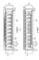
図9は、プローブカード110の第1の面110Aに配置される複数のプローブ115を示す図である。 FIG. 9 is a diagram showing a plurality of
図9においては、ウェハ400の全てのNANDチップ420のパッド電極410の数と同数のプローブ115がプローブカード110の第1の面110Aに配置されている場合が例示されている。 9 illustrates the case where the same number of
この場合、ウェハ400内の全てのNANDチップ420の全てのパッド電極410にプローブカード110のプローブ115が一括して接触され、全てのNANDチップ420をコントローラー111-1によって制御することが可能となる。 In this case, all the
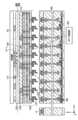
図10は、プローブカード110の第2の面110Bに配置される複数のコントローラー111-1を示す図である。 FIG. 10 is a diagram showing a plurality of controllers 111-1 arranged on the
図10においては、16個のコントローラー111-1(コントローラー111-1-1、111-1-2、…、111-1-16)が配置されている場合が例示されている。1つのウェハ400に1024個のNANDチップ420が含まれ、かつ、プローブカード110の第2の面110Bに16個のコントローラー111-1が配置されている場合においては、各コントローラー111-1は、プローブ115を介して64個のNANDチップ420を制御すればよい。 FIG. 10 illustrates a case where 16 controllers 111-1 (controllers 111-1-1, 111-1-2, . . . , 111-1-16) are arranged. When one
図11は、プローバー100に実装されるデバイス111の一動作例を説明するための図である。 FIG. 11 is a diagram for explaining an operation example of the
ここでは、ウェハ400に形成された複数のNANDチップ420を、複数のコントローラー111-1で分担して制御することを想定する。つまり、プローブカード110上に複数のコントローラー111-1が配置されていることを想定する。 Here, it is assumed that a plurality of
プローブカード110をホスト2(図3参照)などの外部と接続させるためのライザーケーブル111Aが差し込まれるコネクタ111-3が、プローブカード110上に配置される。コネクタ111-3と、複数のコントローラー111-1の中の1つのコントローラー111-1と排他選択的に接続するためのインターフェーススイッチ(たとえばPCIe(登録商標)スイッチ)111-4がプローブカード110上に配置される。インターフェーススイッチ111-4が適切にスイッチングを行うことで、たとえばホスト2からデータの読み出しが要求された際、対応するNANDチップ420を制御するコントローラー111-1へ当該データの読み出しの要求を伝達する。この要求を受けたコントローラー111-1は、NANDチップ420からのデータの読み出しを実行し、読み出したデータをホスト2宛てに送信する。コントローラー111-1から送信されたデータは、インターフェーススイッチ111-4によってコネクタ111-3に中継され、ライザーケーブル111Aを介してホスト2へ転送される。 A connector 111-3 into which a
本実施形態のストレージデバイス1においては、プローブカード110に配置されるこれら複数のデバイス111の温度が、プローブカード110の冷却機構113によって閾値以下に維持される。また、プローバー100上には、コントローラー111-1やインターフェーススイッチ111-4のほか、FPGA、リレー、コンデンサーなどの様々なLSIチップや半導体部品が実装され得る。 In the
次に、ストッカー300に設けられる冷却機構310について説明する。 Next, the
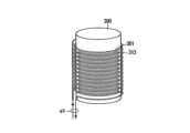
図12は、冷却機構310の第1例を示す図である。 FIG. 12 is a diagram showing a first example of the
ストッカー300には、ウェハ400を出し入れする際に開閉されるシャッター301がウェハ400の保管可能数分設けられる。ストッカー300からウェハ400を取り出したり、ストッカー300へウェハ400を格納したりする際、ストッカー300内の冷気を外へ逃がさないように、複数のシャッター301の中の任意のシャッター301が選択的に開閉されるようになっている。なお、シャッター301を1つとし、内部に保管されているストレージ(ウェハ400)ストック全体を内部で上下に移動させる構成としてもよい。 The
第1例では、ストッカー300に、冷却空気d1を送り込むための吸気口311と、ストッカー300内を貫流した冷却空気d2を排出するための排気口312とを設ける。冷却空気d1は、たとえば高圧で冷却された空気である。本例におけるストッカー300の冷却機構310は、シャッター301によってウェハ400の出入口を閉じ、吸気口311から冷却空気d1を送り続け、常温以下の状態が保たれている冷却空気d1でストッカー300内を満たし続けることで、ストッカー300全体を冷却する。つまり、データの長期保存に適した温度となるように、ストッカー300内のウェハ400を冷却する。 In the first example, the
図13は、冷却機構310の第2例を示す図である。 FIG. 13 is a diagram showing a second example of the
第2例では、冷媒e1を流通させる冷却管313を、たとえば、ストッカー300の側面全体を覆うように、ストッカー300の側面周壁に設ける。冷媒e1は、電子冷却によって冷却された水や液体窒素などである。本例におけるストッカー300の冷却機構310は、シャッター301によってウェハ400の出入口を閉じ、ストッカー300の周壁に設けられる冷却管313に冷媒e1を流通させ、ストッカー300内の空気を冷却することで、ストッカー300全体を冷却する。つまり、データの長期保存に適した温度となるように、ストッカー300内のウェハ400を冷却する。なお、冷却管313は、ストッカー300の内側にあってもよい。 In the second example, a
また、冷却空気d1や冷媒e1を使用する以外にも、たとえば、ストッカー300内でウェハ400を支持する部分、この支持部分に連結する部分、あるいは、ストッカー300全体に、ペルチェ素子を用いた電子冷却機構を設けて、ストッカー300内のウェハ400を冷却してもよい。 In addition to using the cooling air d1 and the coolant e1, for example, electronic cooling using a Peltier element may be applied to the portion supporting the
このように、ストッカー300に冷却機構310を設ける本実施形態のストレージデバイス1においては、データの長期保存に適した常温以下の低温を維持しながら、ストッカー300でウェハ400を保管することが可能である。 Thus, in the
次に、空調制御機構500(図1参照)について説明する。 Next, the air conditioning control mechanism 500 (see FIG. 1) will be described.
前述したように、ストッカー300内のウェハ400は、常温以下の低温に冷却されている。従って、プローバー100内のウェハ400をストッカー300内のウェハ400と入れ替えるために、ストッカー300からウェハ400が取り出されて、当該ウェハ400がプローバー100まで搬送された場合、ストレージ搬送システム200内の空気中の水蒸気が低温のウェハ400上やウェハ400を搬送するストレージ搬送機210上において凝結する(すなわち結露が発生する)可能性がある。この結露防止のために、本実施形態のストレージデバイス1では、空調制御機構500を設けて、ストレージ搬送システム200内の気相雰囲気を、水を含まない乾燥空気、希ガス、不活性ガスなどに置換する。 As described above, the
空調制御機構500は、ストレージ搬送システム200内のみならず、プローバー100内やストッカー300内の気相雰囲気を、水を含まない乾燥空気、希ガス、不活性ガスなどに置換する。これにより、本実施形態のストレージデバイス1においては、ウェハ400上での結露をほぼ完全に防止することができる。なお、ウェハ400を扱う空間内は、水に加えて酸素もないことが好ましいので、プローバー100内、ストレージ搬送システム200内、ストッカー300内の気相雰囲気は、希ガスや不活性ガスなどに置換することが好ましい。 The air-
また、ストッカー300内だけでなく、プローバー100内において常温以上の高温に維持されていたウェハ400をストッカー300まで搬送するストレージ搬送システム200内も冷却されていることが好ましく、前述したように、当該ストレージ搬送システム200内に冷却機構を設けてもよい。 In addition, it is preferable that not only the inside of the
さらには、ストッカー300は、電荷保持特性を長時間維持するために冷却する。その温度は、通常室温となるが、冷却するほど電荷保持特性が高いため、0℃以下も想定し得る。ただし、0℃以下の低温においては、大気中の水が凝縮することによる電気的な副作用、たとえば配線間がショートするなどが考えられる。この観点からも、ストッカー300内の気相雰囲気を、水を含まない乾燥空気、アルゴンなどの希ガス、窒素などの不活性ガスに置換することが好ましい。 Furthermore, the
このように、温度制御機構の一種である空調制御機構500を設ける本実施形態のストレージデバイス1においては、ウェハ400上およびストレージ搬送機210上などでの結露防止を図ることができる。 Thus, in the
図14は、本実施形態のストレージデバイス1が実行するウェハ400の入れ替え時における温度制御の流れの一例を示すフローチャートである。 FIG. 14 is a flow chart showing an example of the flow of temperature control performed by the
ストレージデバイス1は、駆動部130によって、ステージ120上のウェハ400をプローブカード110と電気的に切断する(S1)。ストレージデバイス1は、プローブカード110と電気的に切断されたウェハ400をステージ120上で冷却する(S2)。この際、コントローラー111-1は、例えばI2Cバスを通じて温度計(430、1201)から温度を取得する。ストレージデバイス1は、たとえば常温以下に冷却したウェハ400を、ストレージ搬送システム200によって、プローバー100からストッカー300へ搬送する(S3)。The
続いて、ストレージデバイス1は、プローバー100から取り出したウェハ400と入れ替えでプローバー100へ収容すべきウェハ400を、ストレージ搬送システム200によって、ストッカー300からプローバー100へ搬送する(S4)。ストレージデバイス1は、プローブカード110と電気的に接続するウェハ400を、ステージ上で昇温する(S5)。この際も、コントローラー111-1は、例えばI2Cバスを通じて温度計(430、1201)から温度を取得する。ストレージデバイス1は、たとえばNANDチップ420に対するデータの書き込みや読み出しに適した常温以上に昇温したウェハ400を、駆動部130によって、プローブカード110と電気的に接続する(S6)。Subsequently, the
以上のように、プローバー100、ストレージ搬送システム200およびストッカー300の各々に温度制御機構を設ける本実施形態のストレージデバイス1は、ウェハ400に関する様々な温度制御を適切に行うことができる。 As described above, the
また、プローバー100のステージ120に設けられる加熱冷却機構121は、ウェハ400のリフレッシュに利用することができる。リフレッシュは、NANDチップ内のセルにデータを書き込んだり読み出したりする際のセル間のばらつきが、読み書きストレスで劣化したものを回復させるための処理である。この処理により、NANDチップのデータ保持機能も回復する。たとえば、約300℃のアニールによる劣化回復を図るために、ウェハ400をステージ120上で昇温し、リフレッシュを行う。このために、プローバー100内に設けられる吸気口と、プローバー100内に設けられる、窒素、アルゴン、ヘリウム、クリプトン、キセノンなどの供給機構を用いて、これらの不活性ガスでプローバー100内を封止する。つまり、大気中に含まれる水および酸素濃度を低減する。なお、プローバー100内のエリア別に違う雰囲気で封止してもよい。このように、雰囲気を不活性ガスで置き換えて、ステージ120に設けられる加熱冷却機構121を利用することで、ウェハ400の電極の酸化防止を図ることができる。換言すれば、本実施形態のストレージデバイス1は、ウェハ400をステージ120上で昇温し、ウェハ400の周囲を不活性ガスで封止するリフレッシュ機構をプローバー100に備えてもよい。 Also, the heating and
本発明のいくつかの実施形態を説明したが、これらの実施形態は、例として提示したものであり、発明の範囲を限定することは意図していない。これら新規な実施形態は、その他の様々な形態で実施されることが可能であり、発明の要旨を逸脱しない範囲で、種々の省略、置き換え、変更を行うことができる。これら実施形態やその変形は、発明の範囲や要旨に含まれるとともに、特許請求の範囲に記載された発明とその均等の範囲に含まれる。 While several embodiments of the invention have been described, these embodiments have been presented by way of example and are not intended to limit the scope of the invention. These novel embodiments can be implemented in various other forms, and various omissions, replacements, and modifications can be made without departing from the scope of the invention. These embodiments and modifications thereof are included in the scope and gist of the invention, and are included in the scope of the invention described in the claims and equivalents thereof.
1…ストレージデバイス、2…ホスト、100…プローバー、110…プローブカード、111…デバイス、112…加熱冷却機構、113…冷却機構、114…断熱材、115…プローブ、120…ステージ、121…加熱冷却機構、130…駆動部、200…ストレージ搬送システム、210…ストレージ搬送機、300…ストッカー、310…冷却機構、400…ウェハ、410…パッド電極、420…NANDチップ、430…ウェハ内温度計、500…空調制御機構、1104…プローブカード内温度計、1111…デバイス内温度計、1201…ステージ内温度計。
Claims (21)
Translated fromJapanese前記制御装置から抜脱されている状態にある複数の前記ストレージ媒体を格納するストッカーと、を具備し、
前記制御装置は、前記ストレージ媒体を第1温度以上に昇温するための第1温度制御機構を有し、
前記ストッカーは、前記ストレージ媒体を前記第1温度より低い第2温度以下に冷却するための第2温度制御機構を有する、
ストレージデバイス。a control device that writes data to a storage medium containing a plurality ofNAND flash memory chips or reads data from the storage medium;
a stocker that stores the plurality of storage media that are removed from the control device;
The control device has a first temperature control mechanism for raising the temperature of the storage medium to a first temperature or higher,
The stocker has a second temperature control mechanism for cooling the storage medium to a second temperature lower than the first temperature,
storage device.
前記ストレージ媒体を保持するステージと、
前記ステージによって保持されている前記ストレージ媒体と対向し、当該対向する第1面に複数のプローブを有するプローブカードと、
前記ステージまたは前記プローブカードの少なくとも一方を移動させて、前記ストレージ媒体の前記プローブカードと対向する面に設けられている複数のパッド電極と前記複数のプローブとを接触させ、または、接触している状態にある前記複数のパッド電極と前記複数のプローブとを分離させる駆動部と、
を有し、
前記ストレージ媒体は、前記第1温度制御機構によって前記ステージ上において前記第1温度以上に昇温された後、前記駆動部によって前記複数のプローブと接触させられる、
請求項1に記載のストレージデバイス。The control device is
a stage holding the storage medium;
a probe card facing the storage medium held by the stage and having a plurality of probes on the facing first surface;
At least one of the stage and the probe card is moved to bring or contact the plurality of pad electrodes provided on the surface of the storage medium facing the probe card and the plurality of probes. a driving unit for separating the plurality of pad electrodes in the state from the plurality of probes;
has
The storage medium is brought into contact with the plurality of probes by the driving unit after being heated to the first temperature or higher on the stage by the first temperature control mechanism,
The storage device of Claim 1.
請求項2に記載のストレージデバイス。The first temperature control mechanism includes a plurality of temperature control mechanisms formed within the stage, and performs different temperature control for each of a plurality of different regions having an area smaller than the surface of the storage medium held by the stage. Is possible,
3. The storage device of claim 2.
請求項3に記載のストレージデバイス。The first temperature control mechanism maintains the temperature of each of the regions of the storage medium within a first range by the plurality of temperature control mechanisms.
4. The storage device of claim 3.
前記第1温度制御機構は、前記第2面に配置される前記複数の半導体部品を冷却するための温度制御機構を含む、請求項2~6のいずれか1項に記載のストレージデバイス。The probe card includes a plurality of semiconductor components arranged on a second surface facing the first surface,
The storage device according to any one of claims 2 to 6, wherein said first temperature control mechanism includes a temperature control mechanism for cooling said plurality of semiconductor components arranged on said second surface.
前記第1温度は、常温であり、
前記搬送システムは、前記第2温度以下に冷却されていた前記ストレージ媒体の前記ストッカーから前記制御装置への搬送時における結露防止を目的とする前記搬送システム内の空気調整を行うための第3温度制御機構を有する、
請求項1または2に記載のストレージデバイス。further comprising a transport system for transporting the storage medium from the control device to the stocker or transporting the storage medium from the stocker to the control device;
The first temperature is normal temperature,
The transport system has a third temperature for adjusting the air inside the transport system for the purpose of preventing dew condensation when transporting the storage medium cooled to the second temperature or lower from the stocker to the control device. having a control mechanism,
3. A storage device according to claim 1 or 2.
前記制御装置は、前記ステージに載置されている前記ストレージ媒体を、第1ストレージ媒体から、前記ストッカー内の第2ストレージ媒体に入れ替える場合、
前記第1温度以上の温度に維持されていた前記第1ストレージ媒体を、前記制御装置内において前記第1温度以下に冷却することと、
前記第2温度以下に冷却されていた前記第2ストレージ媒体を、前記制御装置内において前記第1温度以上に昇温し、前記ステージに載置することと、
を具備する制御方法。A storage medium including a plurality ofNAND flash memory chips is heated to a first temperature or higher, and data is written to the storage medium mounted on the stage, or data is written from the storage medium mounted on the stage. and a stocker that cools and stores the plurality of storage media removed from the control device to a second temperature that is lower than the first temperature and stores A control method comprising:
When the control device replaces the storage medium placed on the stage from the first storage medium to the second storage medium in the stocker,
cooling the first storage medium maintained at a temperature equal to or higher than the first temperature to a temperature equal to or lower than the first temperature in the control device;
raising the temperature of the second storage medium, which has been cooled to the second temperature or lower, to the first temperature or higher in the control device, and placing the medium on the stage;
A control method comprising
前記プローバーから抜脱されている状態にある複数の前記半導体ウェハを格納するストッカーと、を具備し、
前記プローバーは、前記半導体ウェハを第1温度以上に昇温するための第1温度制御機構を有し、
前記ストッカーは、前記半導体ウェハを前記第1温度より低い第2温度以下に冷却するための第2温度制御機構を有する、
ストレージデバイス。a prober that writes data to or reads data from a semiconductor wafer including a plurality ofNAND flash memory chips;
a stocker that stores the plurality of semiconductor wafers that have been removed from the prober;
The prober has a first temperature control mechanism for raising the temperature of the semiconductor wafer to a first temperature or higher,
The stocker has a second temperature control mechanism for cooling the semiconductor wafer to a second temperature lower than the first temperature,
storage device.
Applications Claiming Priority (1)
| Application Number | Priority Date | Filing Date | Title |
|---|---|---|---|
| PCT/JP2019/044931WO2021095251A1 (en) | 2019-11-15 | 2019-11-15 | Storage device and control method |
Publications (3)
| Publication Number | Publication Date |
|---|---|
| JPWO2021095251A1 JPWO2021095251A1 (en) | 2021-05-20 |
| JPWO2021095251A5 JPWO2021095251A5 (en) | 2022-04-13 |
| JP7293389B2true JP7293389B2 (en) | 2023-06-19 |
Family
ID=75912115
Family Applications (1)
| Application Number | Title | Priority Date | Filing Date |
|---|---|---|---|
| JP2021555761AActiveJP7293389B2 (en) | 2019-11-15 | 2019-11-15 | Storage device and control method |
Country Status (6)
| Country | Link |
|---|---|
| US (1) | US12384624B2 (en) |
| EP (1) | EP4060721A4 (en) |
| JP (1) | JP7293389B2 (en) |
| CN (1) | CN114424331B (en) |
| TW (2) | TWI800355B (en) |
| WO (1) | WO2021095251A1 (en) |
Citations (1)
| Publication number | Priority date | Publication date | Assignee | Title |
|---|---|---|---|---|
| JP2005181222A (en) | 2003-12-22 | 2005-07-07 | Renesas Technology Corp | Manufacturing method for semiconductor device |
Family Cites Families (34)
| Publication number | Priority date | Publication date | Assignee | Title |
|---|---|---|---|---|
| GB2082354B (en) | 1980-08-21 | 1984-04-11 | Burroughs Corp | Improvements in or relating to wafer-scale integrated circuits |
| US6288561B1 (en)* | 1988-05-16 | 2001-09-11 | Elm Technology Corporation | Method and apparatus for probing, testing, burn-in, repairing and programming of integrated circuits in a closed environment using a single apparatus |
| KR0155158B1 (en)* | 1989-07-25 | 1998-12-01 | 카자마 젠쥬 | Vertical processing device and processing method |
| JP2907971B2 (en)* | 1990-08-14 | 1999-06-21 | 株式会社東芝 | Method for forming or testing semiconductor device pattern |
| JP3435410B2 (en)* | 1996-05-09 | 2003-08-11 | 東京エレクトロン株式会社 | Low temperature test equipment and low temperature test method |
| US6063640A (en) | 1997-03-18 | 2000-05-16 | Fujitsu Limited | Semiconductor wafer testing method with probe pin contact |
| SG98373A1 (en)* | 1998-11-25 | 2003-09-19 | Advantest Corp | Device testing apparatus |
| TW533316B (en)* | 1998-12-08 | 2003-05-21 | Advantest Corp | Testing device for electronic device |
| US6499121B1 (en) | 1999-03-01 | 2002-12-24 | Formfactor, Inc. | Distributed interface for parallel testing of multiple devices using a single tester channel |
| US6499777B1 (en)* | 1999-05-11 | 2002-12-31 | Matrix Integrated Systems, Inc. | End-effector with integrated cooling mechanism |
| DE10343525B4 (en)* | 2002-09-27 | 2011-06-16 | Qimonda Ag | Method for operating semiconductor components, control device for semiconductor components and arrangement for operating memory components |
| JP2005228788A (en) | 2004-02-10 | 2005-08-25 | Seiko Epson Corp | Method for aligning wafer and probe card, probe inspection method and probe inspection apparatus |
| US8084400B2 (en)* | 2005-10-11 | 2011-12-27 | Intermolecular, Inc. | Methods for discretized processing and process sequence integration of regions of a substrate |
| JP2006242766A (en)* | 2005-03-03 | 2006-09-14 | Sanyo Electric Co Ltd | Apparatus for measuring parts temperature |
| JP2006250579A (en)* | 2005-03-08 | 2006-09-21 | Denso Corp | Inspection device and characteristic adjusting method of humidity sensor |
| KR20060127662A (en) | 2005-06-08 | 2006-12-13 | 삼성전자주식회사 | Side storage temperature control device for semiconductor equipment |
| JP2007096190A (en) | 2005-09-30 | 2007-04-12 | Seiko Epson Corp | Probe card needle tip polishing method and probe device |
| US8019938B2 (en) | 2006-12-06 | 2011-09-13 | Fusion-I0, Inc. | Apparatus, system, and method for solid-state storage as cache for high-capacity, non-volatile storage |
| JP4917981B2 (en) | 2007-07-10 | 2012-04-18 | 東京エレクトロン株式会社 | Inspection method and program recording medium recording inspection method |
| JP5374246B2 (en) | 2009-06-12 | 2013-12-25 | 学校法人慶應義塾 | Sealed semiconductor recording medium and sealed semiconductor recording device |
| WO2011027392A1 (en)* | 2009-09-02 | 2011-03-10 | 株式会社アドバンテスト | Testing apparatus, testing method, and program |
| TWI451106B (en)* | 2012-03-26 | 2014-09-01 | Silicon Motion Inc | Wafer testing system and testing method thereof |
| JP2013221911A (en)* | 2012-04-19 | 2013-10-28 | Seiko Epson Corp | Handler and component inspection device |
| JP2014052785A (en)* | 2012-09-06 | 2014-03-20 | Toshiba Corp | Memory system |
| JP6262148B2 (en)* | 2012-12-07 | 2018-01-17 | 株式会社日立国際電気 | Substrate processing apparatus, substrate processing method, semiconductor device manufacturing method, and control program |
| JP6205225B2 (en)* | 2013-03-25 | 2017-09-27 | 東京エレクトロン株式会社 | Substrate inspection apparatus and substrate temperature adjustment method |
| TWI628449B (en)* | 2017-05-05 | 2018-07-01 | 漢民科技股份有限公司 | Active wafer prober pre-heat & pre-cold system and methodology of wafer inspection |
| US10366967B2 (en) | 2017-07-24 | 2019-07-30 | Cerebras Systems Inc. | Apparatus and method for multi-die interconnection |
| JP6827385B2 (en)* | 2017-08-03 | 2021-02-10 | 東京エレクトロン株式会社 | Inspection system |
| US10872789B2 (en) | 2017-09-28 | 2020-12-22 | Taiwan Semiconductor Manufacturing Co., Ltd. | Wafer cooling system |
| US11062886B2 (en)* | 2017-11-28 | 2021-07-13 | Taiwan Semiconductor Manufacturing Co., Ltd. | Apparatus and method for controlling wafer uniformity |
| JP7181068B2 (en)* | 2018-11-30 | 2022-11-30 | 株式会社Screenホールディングス | Substrate processing equipment |
| JP7274350B2 (en)* | 2019-05-28 | 2023-05-16 | 東京エレクトロン株式会社 | Conveyance system, inspection system and inspection method |
| JP7267111B2 (en)* | 2019-05-31 | 2023-05-01 | 東京エレクトロン株式会社 | Positioning mechanism and positioning method |
- 2019
- 2019-11-15JPJP2021555761Apatent/JP7293389B2/enactiveActive
- 2019-11-15CNCN201980100500.3Apatent/CN114424331B/enactiveActive
- 2019-11-15WOPCT/JP2019/044931patent/WO2021095251A1/ennot_activeCeased
- 2019-11-15EPEP19952453.9Apatent/EP4060721A4/enactivePending
- 2020
- 2020-08-12TWTW111115173Apatent/TWI800355B/enactive
- 2020-08-12TWTW109127283Apatent/TWI765316B/enactive
- 2022
- 2022-03-14USUS17/694,532patent/US12384624B2/enactiveActive
Patent Citations (1)
| Publication number | Priority date | Publication date | Assignee | Title |
|---|---|---|---|---|
| JP2005181222A (en) | 2003-12-22 | 2005-07-07 | Renesas Technology Corp | Manufacturing method for semiconductor device |
Also Published As
| Publication number | Publication date |
|---|---|
| TW202230579A (en) | 2022-08-01 |
| US20220204270A1 (en) | 2022-06-30 |
| EP4060721A1 (en) | 2022-09-21 |
| EP4060721A4 (en) | 2023-08-09 |
| CN114424331B (en) | 2025-07-11 |
| WO2021095251A1 (en) | 2021-05-20 |
| US12384624B2 (en) | 2025-08-12 |
| JPWO2021095251A1 (en) | 2021-05-20 |
| TWI765316B (en) | 2022-05-21 |
| TW202127561A (en) | 2021-07-16 |
| TWI800355B (en) | 2023-04-21 |
| CN114424331A (en) | 2022-04-29 |
Similar Documents
| Publication | Publication Date | Title |
|---|---|---|
| US8905700B2 (en) | Transfer and inspection devices of object to be inspected | |
| JP4789125B2 (en) | Electronic component test socket and electronic component test apparatus using the same | |
| JP5615852B2 (en) | Electronic device test system | |
| US7554350B2 (en) | Burn-in system with heating blocks accommodated in cooling blocks | |
| JP5535492B2 (en) | Semiconductor integrated circuit inspection apparatus and semiconductor integrated circuit inspection method | |
| CN101137911A (en) | Method and apparatus for testing semiconductor wafers using a temperature adjustable chuck device | |
| KR20080053768A (en) | Wafer chuck, apparatus and method for testing electrical properties of a wafer comprising the same | |
| KR102592324B1 (en) | Test apparatus of semiconductor package | |
| TWI475234B (en) | Inspection machine with fan-shaped turntable transmission equipment | |
| US20200166562A1 (en) | Inspection apparatus, temperature control device and temperature control method | |
| US20180231582A1 (en) | Transfer unit and prober | |
| JP3901570B2 (en) | Low temperature testing equipment for semiconductor devices using electronic cooling elements | |
| JP2014105996A (en) | Semiconductor device tester and test method | |
| US11454664B2 (en) | Testing system | |
| JP2007294665A (en) | Probe card transfer method, prober and probe card supply/recovery system | |
| KR101474951B1 (en) | Apparatus for testing semiconductor device | |
| JP2016164981A (en) | Transfer unit and prober | |
| JP2024038105A (en) | Prober | |
| JP2016181601A (en) | Prober and wafer chuck temperature measurement method | |
| JP7293389B2 (en) | Storage device and control method | |
| KR102592544B1 (en) | Inspection apparatus and inspection method | |
| JP2000294606A (en) | Inspecting device for semiconductor wafer | |
| JP7535435B2 (en) | Inspection device and probe polishing method | |
| JP2016180680A (en) | Probe card type temperature sensor | |
| JP2003028920A (en) | Electronic component contactor |
Legal Events
| Date | Code | Title | Description |
|---|---|---|---|
| A521 | Request for written amendment filed | Free format text:JAPANESE INTERMEDIATE CODE: A523 Effective date:20220111 | |
| A621 | Written request for application examination | Free format text:JAPANESE INTERMEDIATE CODE: A621 Effective date:20220111 | |
| A131 | Notification of reasons for refusal | Free format text:JAPANESE INTERMEDIATE CODE: A131 Effective date:20221011 | |
| A521 | Request for written amendment filed | Free format text:JAPANESE INTERMEDIATE CODE: A523 Effective date:20221028 | |
| A131 | Notification of reasons for refusal | Free format text:JAPANESE INTERMEDIATE CODE: A131 Effective date:20230117 | |
| A521 | Request for written amendment filed | Free format text:JAPANESE INTERMEDIATE CODE: A523 Effective date:20230130 | |
| TRDD | Decision of grant or rejection written | ||
| A01 | Written decision to grant a patent or to grant a registration (utility model) | Free format text:JAPANESE INTERMEDIATE CODE: A01 Effective date:20230509 | |
| A61 | First payment of annual fees (during grant procedure) | Free format text:JAPANESE INTERMEDIATE CODE: A61 Effective date:20230607 | |
| R151 | Written notification of patent or utility model registration | Ref document number:7293389 Country of ref document:JP Free format text:JAPANESE INTERMEDIATE CODE: R151 |