JP7284593B2 - current drive circuit - Google Patents
current drive circuitDownload PDFInfo
- Publication number
- JP7284593B2 JP7284593B2JP2019034836AJP2019034836AJP7284593B2JP 7284593 B2JP7284593 B2JP 7284593B2JP 2019034836 AJP2019034836 AJP 2019034836AJP 2019034836 AJP2019034836 AJP 2019034836AJP 7284593 B2JP7284593 B2JP 7284593B2
- Authority
- JP
- Japan
- Prior art keywords
- transistor
- current
- gate
- circuit
- node
- Prior art date
- Legal status (The legal status is an assumption and is not a legal conclusion. Google has not performed a legal analysis and makes no representation as to the accuracy of the status listed.)
- Active
Links
Images


Landscapes
- Control Of Electrical Variables (AREA)
- Logic Circuits (AREA)
- Amplifiers (AREA)
- Led Devices (AREA)
Description
Translated fromJapanese本発明の実施形態は、電流駆動回路に関する。 Embodiments of the present invention relate to current driver circuits.
液晶パネルのバックライト等に用いられるLED(Light Emitting Device)は、通電電流の大小で演色が変化するため、想定した演色で発光させるには、LEDに与える電流を高精度に制御する必要がある。その制御された電流で発光するLEDの調光は、LEDに与える電流のパルス幅制御により行われる。パルス電流の周波数が人間の可聴域にあると電源回路などで不快な音が発生する要因になることがあり、対策として、商用電源の周波数よりはるかに高い超音波領域の周波数にすることが多い。また、必要な光度を得るために、複数のLEDを直列駆動する必要があり、駆動電源の出力電圧が数十V以上になる場合がある。 The color rendering of LEDs (Light Emitting Devices), which are used for the backlight of liquid crystal panels, etc., changes depending on the magnitude of the current flowing through them. Therefore, in order to emit light with the expected color rendering, it is necessary to control the current given to the LEDs with high precision. . Dimming of the LED, which emits light with the controlled current, is performed by pulse width control of the current applied to the LED. If the frequency of the pulse current is in the human audible range, it may cause unpleasant sounds in the power supply circuit, etc. As a countermeasure, it is often set to an ultrasonic frequency that is much higher than the frequency of the commercial power supply. . In addition, in order to obtain the required luminous intensity, it is necessary to drive a plurality of LEDs in series, and the output voltage of the drive power source may be several tens of volts or more.
LEDをパルス幅制御によりオン・オフ駆動すると、LEDに電流を与える電流駆動回路のLED接続端子の電圧が大きく変動するが、演色と調光に影響しないように、出力電圧が大きく変動しても電流駆動回路の出力電流は精度を維持することが望ましい。 When the LED is turned on and off by pulse width control, the voltage at the LED connection terminal of the current drive circuit that supplies current to the LED fluctuates greatly. It is desirable to maintain accuracy in the output current of the current driver circuit.
本発明の一実施形態は、出力電圧が変動しても、出力電流を高精度に維持できる電流駆動回路を提供するものである。 One embodiment of the present invention provides a current driver circuit that can maintain an output current with high accuracy even if the output voltage fluctuates.
本実施形態によれば、電流を出力する第1トランジスタと、前記第1トランジスタにカスコード接続される第2トランジスタと、
前記第2トランジスタにカスコード接続される第3トランジスタと、
前記第3トランジスタ及び前記第2トランジスタに電流を供給する第1電流源と、
前記第3トランジスタとゲート同士を共通にする第4トランジスタと、
前記第2トランジスタとゲート同士を共通にし、前記第4トランジスタにカスコード接続される第5トランジスタと、
前記第4トランジスタ及び前記第5トランジスタに電流を供給する第2電流源と、
前記第3トランジスタ及び前記第4トランジスタとゲート同士を共通にし、前記第1トランジスタのゲート電圧を制御する第6トランジスタと、
前記第6トランジスタのドレイン電流を供給する第3電流源と、を備える、電流駆動回路が提供される。According to this embodiment, a first transistor that outputs a current, a second transistor that is cascode-connected to the first transistor,
a third transistor cascode-connected to the second transistor;
a first current source that supplies current to the third transistor and the second transistor;
a fourth transistor having a common gate with the third transistor;
a fifth transistor having a common gate with the second transistor and being cascode-connected to the fourth transistor;
a second current source that supplies current to the fourth transistor and the fifth transistor;
a sixth transistor that shares gates with the third transistor and the fourth transistor and controls the gate voltage of the first transistor;
and a third current source for supplying the drain current of the sixth transistor.
以下、図面を参照して本開示の一実施の形態について説明する。なお、本件明細書に添付する図面においては、図示と理解のしやすさの便宜上、適宜縮尺および縦横の寸法比等を、実物のそれらから変更し誇張してある。 An embodiment of the present disclosure will be described below with reference to the drawings. In addition, in the drawings attached to this specification, for the convenience of illustration and ease of understanding, the scale and the ratio of vertical and horizontal dimensions are appropriately changed and exaggerated from those of the real thing.
さらに、本明細書において用いる、形状や幾何学的条件並びにそれらの程度を特定する、例えば、「平行」、「直交」、「同一」等の用語や長さや角度の値等については、厳密な意味に縛られることなく、同様の機能を期待し得る程度の範囲を含めて解釈することとする。 Furthermore, the terms used herein to specify shapes and geometric conditions and their degrees, such as "parallel", "perpendicular", "identical", length and angle values, etc., are not strictly defined. It shall be interpreted to include the extent to which similar functions can be expected without being bound by the meaning.
(第1の実施形態)
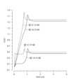
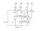
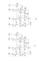
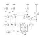
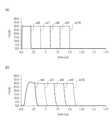
図1Aは第1の実施形態による電流駆動回路100の回路図である。図1Aの電流駆動回路100は、例えばLEDドライバに内蔵されるが、その用途は、LEDの駆動に限定されるものではない。図1Bは図1Aの電流駆動回路100内の電気的特性を示すグラフ(graph1~graph6)である。graph1~graph6の横軸は出力電圧(V)である。graph1の縦軸は第1トランジスタM1のドレイン電流、graph2~6の縦軸はN1、N2、N4、N8、N3の電圧(V)である。(First embodiment)
FIG. 1A is a circuit diagram of a
図1Aの電流駆動回路100は、電流出力の高耐圧の第1トランジスタM1を駆動する回路である。図1Aの電流駆動回路100は、第1トランジスタM1よりも耐圧が低い第2~第6トランジスタM2~M6と、第1~第3電流源1~3とを備えている。図1Aでは、第1~第6トランジスタM1~M6がn型MOS(Metal-Oxide-Silicon)トランジスタの例を示しているが、p型MOSトランジスタで構成することも可能である。第1~第6トランジスタM1~M6がp型MOSトランジスタの場合は、電源電圧ノードVDDと接地ノードとの間の各トランジスタの接続関係が図1Aとは逆になる。第1トランジスタM1のドレインは、出力端子OUTに接続されており、この出力端子OUTから定電流が出力される。本明細書では、第1~第6トランジスタM1~M6がn型MOSトランジスタである例を説明する。なお、第1トランジスタM1は、必ずしも高耐圧である必要はなく、第2~第6トランジスタM2~M6と同じ耐圧や低耐圧であってもよい。 The
第2トランジスタM2は、第1トランジスタM1にカスコード接続されている。第3トランジスタM3は、第2トランジスタM2にカスコード接続されている。1は、第3トランジスタM3及び第2トランジスタM2に電流を供給する。第1電流源1は、電源電圧ノードVDDと第3トランジスタM3のドレインとの間に介挿されている。第3トランジスタM3のソースは第2トランジスタM2のドレインに接続され、第2トランジスタM2のソースは接地ノードに接続されている。第3トランジスタM3のゲートとドレインは接続されている。 The second transistor M2 is cascode-connected to the first transistor M1. The third transistor M3 is cascode-connected to the second transistor M2. 1 supplies current to the third transistor M3 and the second transistor M2. A first
第4トランジスタM4は、第3トランジスタM3とゲート同士を共通にしている。第5トランジスタM5は、第4トランジスタM4にカスコード接続されている。第2電流源2は、第4トランジスタM4及び第5トランジスタM5に電流を供給する。第2電流源2は、電源電圧ノードVDDと第4トランジスタM4のドレインとの間に介挿されている。第4トランジスタM4のソースは第5トランジスタM5のドレインに接続され、第5トランジスタM5のソースは接地ノードに接続されている。第5トランジスタM5のゲートと第4トランジスタM4のドレインとは接続されている。 The fourth transistor M4 shares a gate with the third transistor M3. The fifth transistor M5 is cascode-connected to the fourth transistor M4. A second
第6トランジスタM6は、第3トランジスタM3及び第4トランジスタM4とゲート同士を共通にしている。第6トランジスタM6は、第1トランジスタM1のゲート電圧を制御する。第3電流源は、第6トランジスタM6に電流を供給する。第3電流源3は、電源電圧ノードVDDと第6トランジスタM6のドレインとの間に介挿されている。第6トランジスタM6のドレインは第1トランジスタM1のゲートに接続されている。第6トランジスタM6のソースと接地ノードとの間には、例えば抵抗素子R1が接続されている。 The sixth transistor M6 shares gates with the third transistor M3 and the fourth transistor M4. The sixth transistor M6 controls the gate voltage of the first transistor M1. A third current source supplies current to the sixth transistor M6. A third
第2トランジスタM2は、第3~第6トランジスタM3~M6よりも(N+1)倍大きいサイズを有する。Nは、例えば数十~数千の値である。また、第1トランジスタM1のサイズも十分に大きいものとする。図1Aでは、第1トランジスタM1のサイズを「×N」と表記しているが、第1トランジスタM1のサイズは、第2トランジスタM2よりも大きくてもよい。 The second transistor M2 has a size (N+1) times larger than that of the third to sixth transistors M3 to M6. N is, for example, a value of tens to thousands. It is also assumed that the size of the first transistor M1 is sufficiently large. In FIG. 1A, the size of the first transistor M1 is indicated as "×N", but the size of the first transistor M1 may be larger than that of the second transistor M2.
図1Aでは、第1トランジスタM1のソースと第2トランジスタM2のドレインとの接続ノードをN1、第3トランジスタM3、第4トランジスタM4及び第6トランジスタM6の共通ゲートをN2、第2トランジスタM2と第5トランジスタM5の共通ゲートをN3、第1トランジスタM1のゲートをN4、第6トランジスタM6のソースをN8としている。 In FIG. 1A, the connection node between the source of the first transistor M1 and the drain of the second transistor M2 is N1, the common gate of the third transistor M3, the fourth transistor M4 and the sixth transistor M6 is N2, the second transistor M2 and the The common gate of the five transistors M5 is N3, the gate of the first transistor M1 is N4, and the source of the sixth transistor M6 is N8.
第3トランジスタM3と第4トランジスタM4はカレントミラー回路を構成するため、第1電流源1からの電流I1の単位電流あたりのM3の(ゲート幅W/ゲート長L)の値を、第2電流源2からの電流I2の単位電流あたりのM4の(ゲート幅W/ゲート長L)の値に等しくする。電流I1は第3トランジスタM3のゲートに繋がるノードN2に流れ、電流I2は第2トランジスタM2のゲートに繋がるノードN3に流れる。 Since the third transistor M3 and the fourth transistor M4 form a current mirror circuit, the value of (gate width W/gate length L) of M3 per unit current of the current I1 from the first
また、第3電流源3からの電流I3の単位電流あたりのM6の(ゲート幅W/ゲート長L)の値を、第1電流源1からの電流I1の単位電流あたりのM3の(ゲート幅W/ゲート長L)の値にすると、図1Bのgraph1に示すように、N1の飽和電位はN8の飽和電位の抵抗R1と電流I3の積で設定できる。 Also, the value of (gate width W/gate length L) of M6 per unit current of the current I3 from the third
N1とN8の飽和電位がほぼ同電位になるのはループrp2の帰還によるが、そのためには連動するN2やN4が電源電圧VDD付近で飽和しないように設定する必要がある。 The fact that the saturation potentials of N1 and N8 become almost the same is due to the feedback of loop rp2, but for this reason, it is necessary to set N2 and N4 that interlock so that they do not saturate near the power supply voltage VDD.
図1Cは、図1Aの回路の一変形例を示す回路図である。図1Cは、N4の再立ち上げ時や、電流源の起動直後のN8をソースフォロア回路70で持ち上げて、ループrp2の帰還でN4が整定するまでの時間を短縮する回路例である。ソースフォロア回路70は、カレントミラー回路を構成するトランジスタM15,M16と、トランジスタM15のソースと接地ノードとの間に接続される抵抗R8と、トランジスタM16のソースと接地ノードとの間に接続される抵抗R9と、トランジスタM16のドレインと電源電圧VDDとの間に接続される電流源71とを有する。トランジスタM15のソースは、トランジスタM6のソースに接続されている。 FIG. 1C is a circuit diagram showing a variation of the circuit of FIG. 1A. FIG. 1C is a circuit example in which the
図1Dは図1Aと図1Cの回路内のN4とN8の電圧波形を示す図である。図1Dに示すように、初期状態でN4が0Vの場合、図1Aの回路では、N4が閾値電圧を超えるまでN8は0.1V付近に留まるが、図1Cの回路では、ソースフォロア回路70でN8が0.4V以上に即座に持ち上げられるため、整定時間が30%程度短くなる。 FIG. 1D shows the voltage waveforms of N4 and N8 in the circuits of FIGS. 1A and 1C. As shown in FIG. 1D, when N4 is 0 V in the initial state, in the circuit of FIG. 1A, N8 stays around 0.1 V until N4 exceeds the threshold voltage, but in the circuit of FIG. Settling time is shortened by about 30% because N8 is immediately raised above 0.4V.
図1Eは、図1Aの回路の他の一変形例を示す回路図である。図1Eは、電源VDDが不十分の場合、LED電流が発生しないようにN4を抵抗R10にてプルダウンする例を示す回路図である。図1Eでは、第6トランジスタM6のドレイン電流が、I3からI3-N4電位/R10に減少する。 FIG. 1E is a circuit diagram showing another variation of the circuit of FIG. 1A. FIG. 1E is a circuit diagram showing an example of pulling down N4 with a resistor R10 so as not to generate an LED current when the power supply VDD is insufficient. In FIG. 1E, the drain current of the sixth transistor M6 decreases from I3 to I3-N4 potential/R10.
図1Fは、図1Aの回路の他の一変形例を示す回路図である。図1Fは図1Eの抵抗R10によるN4電位の減少を、バッファアンプA1で補償する回路例である。すなわち、図1Eの回路では、N4電位が下がり過ぎるため、バッファアンプA1でN4電位を引き上げる動作を行う。バッファアンプA1の出力ノードとN4との間には抵抗R11が接続され、バッファアンプA1の出力ノードと接地ノードとの間には抵抗R12が接続されている。抵抗R12=R10-R11に設定される。 FIG. 1F is a circuit diagram showing another variation of the circuit of FIG. 1A. FIG. 1F is a circuit example in which the buffer amplifier A1 compensates for the decrease in the N4 potential due to the resistor R10 in FIG. 1E. That is, in the circuit of FIG. 1E, since the potential N4 is too low, the buffer amplifier A1 performs an operation to raise the potential N4. A resistor R11 is connected between the output node of the buffer amplifier A1 and N4, and a resistor R12 is connected between the output node of the buffer amplifier A1 and the ground node. Resistor R12 is set to R10-R11.
図2Aは図1Aの電流駆動回路100の一変形例の回路図、図2Bは図2Aの電流駆動回路100内の電気的特性を示すグラフ(graph7~graph12)である。graph7~graph12の横軸は出力電圧(V)である。graph7の縦軸は第1トランジスタM1のドレイン電流、graph8~12の縦軸はN1、N2、N4、N8、N3の電圧(V)である。第7トランジスタM7のサイズを×1から×Aに変更することで、N1、N2、N4、N8、N3の電圧を変化させることが出来るが、これによるOUT端子電流の変化は小さい。 2A is a circuit diagram of a modification of the
図2Aの電流駆動回路100は、抵抗素子R1の代わりに第7トランジスタM7を備えている。第7トランジスタM7は、第3トランジスタM3、第4トランジスタM4及び第6トランジスタM6と共通のゲートを有する。第7トランジスタM7のドレインは第6トランジスタM6のソースに接続され、第7トランジスタM7のソースは接地ノードに接続されている。第7トランジスタM7は、第3~第6トランジスタM3~M6と同程度のサイズを有する。第7トランジスタM7も、第2~第6トランジスタM2~M6と同様に低耐圧であり、例えばNMOSトランジスタである。 The
図2Aの第7トランジスタM7は、図1の抵抗素子R1と同様に、第1トランジスタM1のゲート電圧を発生させるために設けられている。図2Bに示すように、N1の飽和電位はN8の飽和電位のドレイン電流I3における第7トランジスタM7のオーバードライブ電圧で設定できる。図1Bと同様に、N1とN8の飽和電位がほぼ同電位になるのはループrp2の帰還によるが、そのためには連動するN2やN4が電源電圧VDD電位付近で飽和しないように設定する必要がある。 The seventh transistor M7 in FIG. 2A is provided to generate the gate voltage of the first transistor M1, similar to the resistive element R1 in FIG. As shown in FIG. 2B, the saturation potential of N1 can be set by the overdrive voltage of the seventh transistor M7 at the drain current I3 of the saturation potential of N8. Similar to FIG. 1B, the fact that the saturation potentials of N1 and N8 become almost the same is due to the feedback of loop rp2. be.
図2Cは、図2Aの回路の一変形例を示す回路図である。図2Cは、図2Aの第6トランジスタM6と第7トランジスタM7をひとつの第6トランジスタM6にまとめた回路例を示す回路図である。第6トランジスタM6のドレイン電流I3の時のオーバードライブ電圧と閾値電圧の合計が、図2Aにおける第7トランジスタM7のドレイン電流I3のオーバードライブ電圧と第6トランジスタM6のドレイン電流I3のオーバードライブ電圧と閾値電圧との合計と同じになるようにサイズ(ゲート幅W/ゲート長L)を設定する。 FIG. 2C is a circuit diagram showing a variation of the circuit of FIG. 2A. FIG. 2C is a circuit diagram showing a circuit example in which the sixth transistor M6 and the seventh transistor M7 in FIG. 2A are combined into one sixth transistor M6. The sum of the overdrive voltage and the threshold voltage at the time of the drain current I3 of the sixth transistor M6 is the overdrive voltage of the drain current I3 of the seventh transistor M7 and the overdrive voltage of the drain current I3 of the sixth transistor M6 in FIG. 2A. The size (gate width W/gate length L) is set so as to be the same as the sum with the threshold voltage.
図2Dは、図2Aの回路の他の一変形例を示す回路図である。図2Dは、N8の設定を第7トランジスタM7のサイズ設定とI3×R1の両方で行う回路例を示す回路図である。 FIG. 2D is a circuit diagram showing another variation of the circuit of FIG. 2A. FIG. 2D is a circuit diagram showing a circuit example in which setting of N8 is performed by setting both the size of the seventh transistor M7 and I3×R1.
図2Eは、図2Aの回路の他の一変形例を示す回路図である。図2Eは、N4の再立ち上げ時や、電流源の起動直後のN8をソースフォロア回路70で持ち上げて、ループrp2の帰還でN4が整定するまでの時間を短縮する回路例を示す回路図である。図2Eのソースフォロア回路70の回路構成は、図1Cのソースフォロア回路70の抵抗R8,R9をトランジスタM17,M11に置換した以外は同様の回路構成である。 FIG. 2E is a circuit diagram showing another variation of the circuit of FIG. 2A. FIG. 2E is a circuit diagram showing a circuit example for shortening the time until N4 settles by the feedback of loop rp2 by raising N8 by the
図2Fは、図2Aの回路の他の一変形例を示すグラフである。図2Fに示すように、初期状態でN4が0Vの場合、図2Aの回路では、N4が閾値電圧を超えるまでN8は0.1V付近にとどまるが、図2Eの回路では、ソースフォロア回路70でN8が0.2V以上に即座に持ち上げられるため整定時間が20%程度短くなる。 FIG. 2F is a graph showing another variation of the circuit of FIG. 2A. As shown in FIG. 2F, when N4 is 0 V in the initial state, in the circuit of FIG. 2A, N8 remains around 0.1 V until N4 exceeds the threshold voltage, whereas in the circuit of FIG. Settling time is shortened by about 20% because N8 is immediately raised above 0.2V.
図2Gは、図2Aの回路の他の一変形例を示す回路図である。図2Gは、電源VDDが不十分の場合、LED電流が発生しないようにN4をプルダウンする例を示す回路図である。図2Gの回路では、第6トランジスタM6のドレイン電流が、I3からI3-N4電位/R10に減少している。 FIG. 2G is a circuit diagram showing another variation of the circuit of FIG. 2A. FIG. 2G is a circuit diagram showing an example of pulling down N4 so that no LED current occurs when the power supply VDD is insufficient. In the circuit of FIG. 2G, the drain current of the sixth transistor M6 is reduced from I3 to I3-N4 potential/R10.
図2Hは、図2Aの回路の他の一変形例を示す回路図である。図2Hは図2Gの抵抗R10によるN4電位の減少を、バッファアンプA1で補償する回路例である。図2HのバッファアンプA1と、このバッファアンプA1に接続される抵抗R11、R12との関係は、図1Fと同様である。 FIG. 2H is a circuit diagram showing another variation of the circuit of FIG. 2A. FIG. 2H is a circuit example in which the buffer amplifier A1 compensates for the decrease in the N4 potential due to the resistor R10 in FIG. 2G. The relationship between the buffer amplifier A1 in FIG. 2H and the resistors R11 and R12 connected to this buffer amplifier A1 is the same as in FIG. 1F.
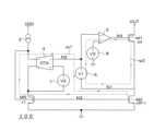
図3は図1A及び図2Aの電流駆動回路100の主要部の等価回路図である。図3の等価回路は、第1トランジスタM1と、第2トランジスタM2と、第5トランジスタM5と、第2電流源2と、OTA(Operational Trans-conductance Amplifier)4と、差動増幅器5と、第1~第3電圧源6~8とを備えている。 FIG. 3 is an equivalent circuit diagram of the main part of the
OTA4は、2つの入力電圧の差に比例した電流を出力する。OTA4の非反転入力端子は、第1電圧源6と差動増幅器5の反転入力端子とに接続されており、ノードN2に対応する。OTA4の反転入力端子は、電圧V2を出力する第2電圧源7に接続されている。OTA4の2つの電流出力端子は、第2電流源2からの電流経路上に介挿されている。
この電流経路上には、第2電流源2と、第5トランジスタM5とが接続されている。差動増幅器5の非反転入力端子には、電圧V3を出力する第3電圧源8が接続されている。差動増幅器5の反転入力端子には、電圧V1を出力する第1電圧源6が接続されている。差動増幅器5の出力端子には、ノードN4を介して第1トランジスタM1のゲートが接続されている。
A second
図3の等価回路は、第2トランジスタM2、OTA4及び第5トランジスタM5を通過する第1制御ループrp1と、差動増幅器5、第1トランジスタM1及び第1電圧源6を通過する第2制御ループrp2とを有する。 The equivalent circuit of FIG. rp2.
第1制御ループrp1では、ノードN1の電位にてノードN3の電位を決定する。また、第1制御ループrp1では、第2トランジスタM2のドレイン電流が、I2×(1+N)≒I2×Nになるように制御する。第2制御ループrp2では、ノードN1が図1A及び図2AのノードN8と同電位になるようにノードN4の電位を制御する。出力電圧VOUTがノードN1の目標電圧(ノードN8の電位=V3-V1)より高い場合は、第2制御ループrp2にてノードN1は目標電圧に維持されるため、ノードN4の電位変動は小さくなる。出力電圧VOUTが目標電圧より低くなると、第2制御ループrp2はノードN4の電位を持ち上げて、ノードN1の電位低下を防ぐように帰還する。このような帰還制御によっても、ノードN1の電位が低下する場合には、第1制御ループrp1がノードN3の電位を持ち上げて、第1トランジスタM1と第2トランジスタM2のドレイン電流を維持するように帰還制御を行う。 In the first control loop rp1, the potential of the node N3 determines the potential of the node N1. Also, in the first control loop rp1, the drain current of the second transistor M2 is controlled so that I2×(1+N)≈I2×N. The second control loop rp2 controls the potential of the node N4 so that the node N1 has the same potential as the node N8 in FIGS. 1A and 2A. When the output voltage VOUT is higher than the target voltage of the node N1 (the potential of the node N8 = V3-V1), the node N1 is maintained at the target voltage in the second control loop rp2, so the potential fluctuation of the node N4 is small. . When the output voltage VOUT becomes lower than the target voltage, the second control loop rp2 raises the potential of the node N4 and feeds back to prevent the potential of the node N1 from dropping. Even with such feedback control, when the potential of the node N1 drops, the first control loop rp1 raises the potential of the node N3 to maintain the drain currents of the first transistor M1 and the second transistor M2. Performs feedback control.
図1A及び図2Aの回路において、第1制御ループrp1は、第4トランジスタM4、第5トランジスタM5、第2トランジスタM2及び第3トランジスタM3を通過する経路である。また、第2制御ループrp2は、第1トランジスタM1、第3トランジスタM3及び第6トランジスタM6を通過する経路である。 In the circuits of FIGS. 1A and 2A, the first control loop rp1 is a path passing through the fourth transistor M4, the fifth transistor M5, the second transistor M2 and the third transistor M3. Also, the second control loop rp2 is a path passing through the first transistor M1, the third transistor M3 and the sixth transistor M6.
図1A及び図2Aの回路は、第1トランジスタM1と第2トランジスタM2のサイズが第3~第7トランジスタM3~M7のサイズよりもはるかに大きいため、電源投入時の起動信号が入力されてから、第1トランジスタM1が電流を出力し始めるまでに時間がかかる。この時間を短縮するための起動補助回路の回路構成には複数通りが考えられる。以下では、起動補助回路の代表的な第1~第5具体例を説明する。 In the circuits of FIGS. 1A and 2A, the sizes of the first transistor M1 and the second transistor M2 are much larger than the sizes of the third to seventh transistors M3 to M7. , it takes time for the first transistor M1 to start outputting current. A plurality of circuit configurations are conceivable for the circuit configuration of the activation assist circuit for shortening this time. In the following, representative first to fifth concrete examples of the activation assist circuit will be described.
(起動補助回路の第1具体例)
起動補助回路の第1具体例は、第2トランジスタM2のゲートに繋がるノードN3の充電電流を一時的に増やすものである。一時的とは、例えば起動信号が入力されてから所定時間である。(First specific example of start-up auxiliary circuit)
A first specific example of the start-up assist circuit temporarily increases the charging current of the node N3 connected to the gate of the second transistor M2. "Temporarily" means, for example, a predetermined time after the activation signal is input.
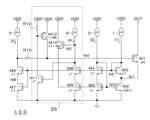
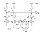
図4は第1具体例による起動補助回路25を備える電流駆動回路100の回路図である。図4の起動補助回路25は、例えば図2Aの電流駆動回路100の回路構成に加えて、第8トランジスタM8と、第9トランジスタM9と、第4電流源9と、第1起動切替器10と、第2起動切替器11とを有する。 FIG. 4 is a circuit diagram of a
第8トランジスタM8は、第3トランジスタM3、第4トランジスタM4及び第6トランジスタM6とゲート同士を共通にする。第9トランジスタM9は、第2トランジスタM2及び第5トランジスタM5とゲート同士を共通にする。第8トランジスタM8のソースは第9トランジスタM9のドレインに接続され、第9トランジスタM9のソースは接地ノードに接続されている。第1起動切替器10は、第4電流源9と第8トランジスタM8のドレインとの間に介挿されている。第2起動切替器11は、第8トランジスタM8のドレインと第4トランジスタM4のドレインとの間に介挿されている。 The eighth transistor M8 shares gates with the third transistor M3, the fourth transistor M4 and the sixth transistor M6. The ninth transistor M9 shares gates with the second transistor M2 and the fifth transistor M5. The source of the eighth transistor M8 is connected to the drain of the ninth transistor M9, and the source of the ninth transistor M9 is connected to the ground node. The
第8トランジスタM8と第9トランジスタM9は、第4トランジスタM4と第5トランジスタM5の(M-1)倍のサイズを有するため、第4電流源9は、第2電流源2の(M-1)倍の電流を流すことができる。 The size of the eighth transistor M8 and the ninth transistor M9 is (M-1) times the size of the fourth transistor M4 and the fifth transistor M5. ) can pass twice as much current.
図4(a)は起動補助回路25が起動補助を行う前の状態を示している。図4(a)の場合、第1起動切替器10と第2起動切替器11がともに接続経路を遮断している。これにより、第8トランジスタM8と第9トランジスタM9は、オフ状態になる。 FIG. 4(a) shows the state before the start-up
図4(b)は起動信号が入力されてから所定期間内に起動補助回路25が起動補助を行う状態を示している。図4(b)の場合、第1起動切替器10と第2起動切替器11がともに接続経路を導通する。これにより、ノードN3には、第8及び第9トランジスタM9と第2電流源2がない場合と比べてM倍の電流が流れ、起動時間を1/Mに短縮できる。
所定期間が経過すると、図4(a)に示すように、第1起動切替器10と第2起動切替器11が接続経路を遮断するため、第8及び第9トランジスタM9と第2電流源2は動作を停止する。FIG. 4(b) shows a state in which the start assist
After a predetermined period of time, as shown in FIG. 4A, the
(起動補助回路25の第2具体例)
起動補助回路25の第2具体例は、起動入力信号が入力されてから所定期間は、ノードN3の電位を高くする制御を行うものである。(Second specific example of start-up auxiliary circuit 25)
A second specific example of the activation assist
図5は第2具体例による起動補助回路25を備える電流駆動回路100の回路図である。図5の起動補助回路25は、例えば、第8~第10トランジスタM8~M10と、第4電流源9とを有する。第8トランジスタM8、第9トランジスタM9及び第4電流源9の接続形態は図4と同様である。第10トランジスタM10のゲートは、第8トランジスタM8のドレインに接続され、第10トランジスタM10のドレインは電源電圧ノードVDDに接続され、第10トランジスタM10のソースは、第2トランジスタM2、第5トランジスタM5及び第9トランジスタM9の共通ゲートに接続されている。この起動補助回路25はN3が所定の電圧になったとき、N5の電位が(N3の電位)+(M10の閾値電圧)未満に確実に下がるように、I4による電流の単位電流あたりの第8トランジスタM8の(ゲート幅W/ゲート長L)は、I2による電流の単位電流あたりの第4トランジスタM4の(ゲート幅W/ゲート長L)以上に設定される。第10トランジスタM10のサイズは、1倍~Ma倍(Ma>1)である。 FIG. 5 is a circuit diagram of a
起動信号が入力されてから所定期間は、第10トランジスタM10のゲートがハイレベルになり、第2、第5及び第9トランジスタM2、M5、M9のゲートに繋がるノードN3の電位が高くなる。第2トランジスタM2のドレイン電流が、定常状態での第2トランジスタM2のドレイン電流のa倍(a<1で、例えばa=0.5)になると、第10トランジスタM10のゲートに繋がるノードN5がローレベルになり、第10トランジスタM10はオフ状態になり、起動補助動作は終了する。 For a predetermined period after the activation signal is input, the gate of the tenth transistor M10 becomes high level, and the potential of the node N3 connected to the gates of the second, fifth and ninth transistors M2, M5 and M9 becomes high. When the drain current of the second transistor M2 becomes a times the drain current of the second transistor M2 in a steady state (a<1, for example a=0.5), the node N5 connected to the gate of the tenth transistor M10 becomes It becomes low level, the tenth transistor M10 is turned off, and the start-up assisting operation ends.
ここで、「起動信号が入力されてから所定期間」、及び「(ドレイン電流の)a倍」の点について以下、補足する。まず、「起動信号が入力されてから所定期間」とは、「ノードN2とノードN3の電位が初期状態で、かつ、直列の第8トランジスタM8と第9トランジスタM9も通電しない初期状態において、第1~第4電流源1~3、9のノードN2~ノードN5への給電が開始された時刻(起動信号の入力時)から、給電によりノードN2~ノードN5が定常状態に近づき直列の第8トランジスタM8と第9トランジスタM9のドレイン電流が第2電流源2の電流のa×(M8のゲート幅W/ゲート長L)/(M4のゲート幅W/ゲート長L)倍に達するまでの期間(所定期間)」である。尚、起動信号の入力は、電流源のオン信号により行われてもよい。 Here, the points of "a predetermined period after the activation signal is input" and "(a times the drain current)" will be supplemented below. First, ``a predetermined period after the activation signal is input'' means ``in an initial state in which the potentials of the nodes N2 and N3 are in an initial state and the serially connected eighth transistor M8 and the ninth transistor M9 are not energized. From the time when the power supply to the nodes N2 to N5 of the 1st to 4th
次に「(ドレイン電流の)a倍」の点について説明する。第4電流源9の電流は、第2電流源2の電流のa×(M8のゲート幅W/ゲート長L)/(M4のゲート幅W/ゲート長L)倍(ただし、a<1で、例えばa=0.5)に設定される。所定期間は、第4電流源9の給電能力が、直列の第8トランジスタM8と第9トランジスタM9のドレイン電流を上回るため、第10トランジスタM10のゲートがハイレベルになり、第2、第5及び第9トランジスタM2、M5、M9のゲートに繋がるノードN3の電位が定常状態に近づくように給電される。所定期間経過後は、直列の第8トランジスタM8と第9トランジスタM9の飽和領域でのドレイン電流が第4電流源9の電流供給能力を超えるため第10トランジスタM10のゲートに繋がるノードN5がローレベルになり、第10トランジスタM10はオフ状態になり、起動補助動作は終了する。そのタイミングは第2トランジスタM2のドレイン電流が、定常状態での第2トランジスタM2のドレイン電流のa倍を超えるときである。 Next, the point of "a times (drain current)" will be described. The current of the fourth
(起動補助回路25の第3具体例)
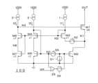
起動補助回路25の第3具体例は、起動入力信号が入力されてから所定期間は、第1トランジスタM1のゲートに繋がるノードN4の電位を高くする制御を行うものである。(Third specific example of start-up auxiliary circuit 25)
A third specific example of the activation assist
図6は第3具体例による起動補助回路25を備える電流駆動回路100の回路図である。図6の起動補助回路25は、例えば第8~第12トランジスタM8~M12と、第4電流源9とを有する。第8~第10トランジスタM8~M10及び第4電流源9の接続形態は図5と同様である。 FIG. 6 is a circuit diagram of a
第12トランジスタM12は、第1~第10トランジスタM1~M10とは導電型が異なっている。第12トランジスタM12は、第1トランジスタM1のゲート電圧を制御する。第11トランジスタM11は、第10トランジスタM10とゲート同士を共通にしている。第12トランジスタM12のゲートは、第11トランジスタM11のドレインに接続されている。第11トランジスタM11のソースは接地ノードに接続されている。第12トランジスタM12のゲートと電源電圧ノードVDDとの間には抵抗素子R12が接続されている。第12トランジスタM12のサイズは、1倍~Mb倍(Mb>1)である。 The twelfth transistor M12 has a conductivity type different from that of the first to tenth transistors M1 to M10. The twelfth transistor M12 controls the gate voltage of the first transistor M1. The eleventh transistor M11 shares a gate with the tenth transistor M10. The gate of the twelfth transistor M12 is connected to the drain of the eleventh transistor M11. The source of the eleventh transistor M11 is connected to the ground node. A resistance element R12 is connected between the gate of the twelfth transistor M12 and the power supply voltage node VDD. The size of the twelfth transistor M12 is 1 to Mb times (Mb>1).
起動信号が入力されてから所定期間は、第10トランジスタM10のゲートがハイレベルになり、第2、第5及び第9トランジスタM2、M5、M9のゲートに繋がるノードN3の電位が高くなる。また、第11トランジスタM11のゲート電位も高くなるため、第12トランジスタM12のゲート電位が下がって、第1トランジスタM1のゲートに繋がるノードN4の電位が高くなる。所定期間が終了し、第2トランジスタM2のゲートに繋がるノードN3の電位がより定常状態に近づき、第2トランジスタM2のドレイン電流が定常状態のa倍(a<1で、例えばa=0.5)を超えると、第10トランジスタM10のゲートに繋がるノードN5がローレベルになり、第10トランジスタM10と第11トランジスタM11はオフ状態になる。これにより、第12トランジスタM12もオフする。 For a predetermined period after the activation signal is input, the gate of the tenth transistor M10 becomes high level, and the potential of the node N3 connected to the gates of the second, fifth and ninth transistors M2, M5 and M9 becomes high. Further, since the gate potential of the eleventh transistor M11 also increases, the gate potential of the twelfth transistor M12 decreases, and the potential of the node N4 connected to the gate of the first transistor M1 increases. After the predetermined period ends, the potential of the node N3 connected to the gate of the second transistor M2 approaches the steady state, and the drain current of the second transistor M2 increases by a times the steady state (a<1, for example, a=0.5). ), the node N5 connected to the gate of the tenth transistor M10 becomes low level, and the tenth transistor M10 and the eleventh transistor M11 are turned off. As a result, the twelfth transistor M12 is also turned off.
図6の一変形例として、図7に示すように、第12トランジスタM12にダーリントン接続される第14トランジスタM14と抵抗素子R13を設けてもよい。 As a modified example of FIG. 6, as shown in FIG. 7, a 14th transistor M14 and a resistance element R13 may be provided that are Darlington-connected to the 12th transistor M12.
上述した基準補助回路の第1具体例と第2具体例では、起動信号が入力されてから所定期間内は、第8トランジスタM8と第9トランジスタM9に、a×I2(a<1)の電流を流すことで、第2トランジスタM2のドレイン電流の立ち上がりを早めているが、第8トランジスタM8のドレインに繋がるノードN5の電位は、起動信号が入力された直後はハイレベルで、その後急速に低下する。ノードN5の電位をモニタすることで、第2トランジスタM2の起動補助を終了するかどうか、すなわち所定期間の終了タイミングを判断できる。 In the first specific example and the second specific example of the reference auxiliary circuit described above, a current of a×I2 (a<1) is applied to the eighth transistor M8 and the ninth transistor M9 within a predetermined period after the start signal is input. , the potential of the node N5 connected to the drain of the eighth transistor M8 is at high level immediately after the start signal is input, and then rapidly drops. do. By monitoring the potential of the node N5, it is possible to determine whether or not to end the activation assistance of the second transistor M2, that is, the end timing of the predetermined period.
図8は図5又は図6の電流駆動回路100内の各部の動作波形である。時刻t0で起動信号が入力されると、第8及び第9トランジスタM8、M9にa×I2の電流が流れて起動補助が行われるため、第2トランジスタM2のゲートに繋がるノードN3の電位(波形w1)は線形に増加する。ノードN3が閾値電圧を超えた時点(時刻t1)以降で、第2トランジスタM2のドレイン電流(波形w2)は急激に増加する。また、第8トランジスタM8のドレインに繋がるノードN5の電位(波形w3)は急激に低下するが、このノードN5の電位が所定電位になった時点を起動補助の終了時刻とすればよい。 FIG. 8 shows operation waveforms of each part in the
(起動補助回路25の第4具体例)
起動補助回路25の第4具体例は、第1トランジスタM1のゲートに繋がるノードN4上と、第2トランジスタM2のゲートに繋がるノードN3上との少なくとも一方に、バッファを介挿するものである。(Fourth specific example of start-up auxiliary circuit 25)
A fourth specific example of the activation assist
図9A及び図9Bは第2トランジスタM2のノードに繋がるノードN3上にバッファを介挿する例を示す起動補助回路25の回路図である。図9A及び図9Bの起動補助回路25は、第1バッファ11と、第2バッファ12と、アナログスイッチ13とを備えている。第1バッファ11と第2バッファ12には、起動信号が入力されるタイミングに同期して、パルス信号XEN、ENが入力される。パルス信号XEN、ENは、入力時の立ち上がり(立ち下がり)エッジは急峻で、終了時の立ち下がり(立ち上がり)は緩やかに変化する信号である。終了時の立ち下がり(立ち上がり)を緩やかに変化させる理由は、オーバーシュートやアンダーシュートの発生を防止して、起動補助動作を緩やかに終了させるためである。 9A and 9B are circuit diagrams of the activation assist
図9Aに示す第1バッファ11は、電源電圧ノードVDDに接続されて電流源として機能するPMOSトランジスタ14と、このPMOSトランジスタ14のドレインと接地ノードとの間にカスコード接続されるPMOSトランジスタ15及びNMOSトランジスタ16と、同じくPMOSトランジスタ14のドレインと接地ノードとの間にカスコード接続されるPMOSトランジスタ17及びNMOSトランジスタ18とを有する。 The
図9Bに示す第1バッファ11は、図9Aのトランジスタ16とトランジスタ18のドレイン電圧を揃えるために、トランジスタ72~76を追加したものであり、第1バッファ11の入出力オフセットを小さくすることができる。 The
図9Aに示す第2バッファ12は、接地ノードに接続されて電流源として機能するNMOSトランジスタ19と、電源電圧ノードVDDとNMOSトランジスタ19のドレインとの間にカスコード接続されるPMOSトランジスタ20及びNMOSトランジスタ21と、同じく電源電圧ノードVDDとNMOSトランジスタ19のドレインとの間にカスコード接続されるPMOSトランジスタ22及びNMOSトランジスタ23とを有する。 The
図9Bに示す第2バッファ12は、図9Aのトランジスタ20とトランジスタ22のドレイン電圧を揃えるために、トランジスタ77~81を追加したものであり、第2バッファ12の入出力オフセットを小さくすることができる。 The
PMOSトランジスタ15のゲートとNMOSトランジスタ21のゲートは、アナログスイッチ13の入力ノードとともに、起動補助回路25の入力端子に接続されている。PMOSトランジスタ17のゲートとNMOSトランジスタ23のゲートは、第2トランジスタM2のゲートに接続されている。 The gate of the
アナログスイッチ13は、パルス信号XEN、ENが入力されると、ノードN3と第2トランジスタM2のゲートとの接続経路を遮断する。パルス信号XEN、ENが入力されなくなると、アナログスイッチ13は、ノードN3と第2トランジスタM2のゲートとを導通する。 The
パルス信号XEN、ENが入力されている期間内は、ノードN3上の信号は、第1バッファ11と第2バッファ12でバッファリングされた後に第2トランジスタM2のゲートに入力される。第1バッファ11と第2バッファ12でバッファリングすることで、第2トランジスタM2のゲート電圧の立ち上がりが急峻になり、第2トランジスタM2の起動時間を短縮できる。パルス信号XEN、ENが入力されなくなると、第1バッファ11と第2バッファ12はバッファリング動作を行わなくなり、ノードN3と第2トランジスタM2のゲートとがアナログスイッチ13を通して導通し、通常動作が行われる。 During the period when the pulse signals XEN and EN are input, the signal on the node N3 is buffered by the
パルス信号XEN、ENは、例えば、起動信号の立ち上がりエッジに同期して生成することができる。図10Aは図9Aの起動補助回路25にパルス発生回路30を追加した回路図、図10Bは図9Bの起動補助回路25にパルス発生回路30を追加した回路図である。図10Aと図10Bのパルス発生回路30は、ワンショットパルス生成器31と、第1波形調整回路32と、第2波形調整回路33とを有する。 The pulse signals XEN and EN can be generated, for example, in synchronization with the rising edge of the activation signal. 10A is a circuit diagram in which a
ワンショットパルス生成器31は、バッファ34と、抵抗素子R2と、キャパシタC1と、インバータ35と、論理ゲート36とを有する。バッファ34には、起動信号が入力される。起動信号が立ち上がると、抵抗素子R2とキャパシタC1で、起動信号の立ち上がり波形をなまらせる。論理ゲートには、起動信号と、起動信号をなまらせた信号とが入力されて、ワンショットパルス信号が生成される。このワンショットパルス信号は、立ち上がりがやや緩やかで、立ち下がりが裾を引くような信号である。 The one-
第1波形調整回路32は、カスコード接続された2つのPMOSトランジスタ37,38と、抵抗素子R3と、キャパシタC2とが並列接続された回路と、この回路に直列接続された抵抗素子R4及びNMOSトランジスタ39とを有する。 The first
第2波形調整回路33は、カスコード接続された2つのNMOSトランジスタ40,41と、抵抗素子R5と、キャパシタC3とが並列接続された回路と、この回路に直列接続された抵抗素子R6及びPMOSトランジスタ42とを有する。 The second
NMOSトランジスタ39のドレインから図9Aと同様のパルス信号XENが出力される。また、PMOSトランジスタの42のドレインから図9Aと同様のパルス信号ENが出力される。 A pulse signal XEN similar to that in FIG. 9A is output from the drain of the
また、図10Aの起動補助回路25は、第1トランジスタM1のゲートを高速起動する高速起動回路43を有する。この高速起動回路43は、PMOSトランジスタ44と、NMOSトランジスタ45と、抵抗素子R7とを有する。PMOSトランジスタ44のソースは電源電圧ノードVDDに接続され、PMOSトランジスタ44のドレインは、NMOSトランジスタ45のゲートと抵抗素子R7の一端とに接続されている。NMOSトランジスタ45のドレインは電源電圧ノードVDDに接続され、NMOSトランジスタ45のソースは、第1トランジスタM1のゲートに繋がるノードN4に接続されている。 10A also includes a high-speed start-up
以上、図1Aで示した第1の実施形態による電流駆動回路100について、いくつかの変形例や具体例を用いて説明してきたが、これらの電流駆動回路100は、少なくとも、サイズの大きい高耐圧の第1トランジスタM1にカスコード接続されたサイズの大きい低耐圧の第2トランジスタM2を駆動するために、第3~第6トランジスタM3~M6を有する。第2~第5トランジスタM2~M5は、ノードN1の電位にてノードN3の電位を決定し、第2トランジスタM2のドレイン電流が約I2×Nとなるように制御する第1制御ループrp1を構成する。また、第3トランジスタM3と第6トランジスタM6は、第1トランジスタM1のソースと第2トランジスタM2のドレインが繋がるノードN1が第6トランジスタM6のソースが繋がるノードN6と同電位になるように制御する第2制御ループrp2を構成する。このような第1制御ループrp1と第2制御ループrp2を設ける構成とすることで、出力電圧VOUTが大きく変動しても、出力端子OUTから定電流を出力できる。 The
また、図9A及び図10Aで説明したように、第1の実施形態による電流駆動回路100において、その回路内部に起動補助回路25を追加して設けることができる。起動補助回路25を設けることで、第1トランジスタM1が電流を出力し始めるまでの時間を短縮できる。起動補助回路25は、起動信号が入力されてから所定期間のみ動作し、所定期間が経過すると、動作を停止するため、消費電力が増えるおそれはない。 Further, as described with reference to FIGS. 9A and 10A, the
(第2の実施形態)
第2の実施形態は、図1Aの電流駆動回路100に、高速化のための回路を追加するものである。(Second embodiment)
The second embodiment adds a circuit for speeding up to the
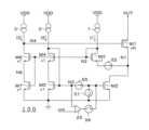
図11は第2の実施形態による電流駆動回路100の回路図である。図11の電流駆動回路100は、図1Aの電流駆動回路100の回路構成に加えて、第8~第12トランジスタM8~M12と、第4電流源9と、抵抗素子R1とを備えている。第8~第12トランジスタM8~M12と、第4電流源9と、抵抗素子R1との接続関係は、図6と同様であるため、説明を省略する。 FIG. 11 is a circuit diagram of the
抵抗素子R1の抵抗値は、ノードN1の静定電位を第3電流源3が出力する電流I3で割った値に設定される。第2電流源2が出力する電流I2と第3電流源3が出力する電流I3との電流比は、第4トランジスタM4と第6トランジスタM6の電流ミラー比に設定される。 The resistance value of the resistance element R1 is set to a value obtained by dividing the static potential of the node N1 by the current I3 output by the third
図11の第3トランジスタM3、第4トランジスタM4及び第5トランジスタM5は、第2トランジスタM2のゲート電圧発生回路を構成している。また、第6トランジスタM6、第7トランジスタM7及び第3電流源3は、第1トランジスタM1のゲート電圧発生回路を構成している。 A third transistor M3, a fourth transistor M4 and a fifth transistor M5 in FIG. 11 constitute a gate voltage generating circuit for the second transistor M2. The sixth transistor M6, the seventh transistor M7 and the third
図12は図11の一変形例による電流駆動回路100の回路図である。図12の電流駆動回路100は、図11の抵抗素子R1の代わりに第7トランジスタM7を備えている。
第7トランジスタM7の接続関係は、図2Aと同様である。FIG. 12 is a circuit diagram of a
The connection relationship of the seventh transistor M7 is the same as in FIG. 2A.
第2電流源2が出力する電流I2と第3電流源3が出力する電流I3との比は、第4トランジスタM4と第6トランジスタM6のゲート幅W/ゲート長Lの比で設定される。同様に、第5トランジスタM5と第7トランジスタM7のW/Lも同じ比に設定される。この比を調整することで、第1トランジスタM1のゲート電圧を調整でき、第1トランジスタM1のドレイン電流(電流駆動回路100の出力電流)を調整できる。出力電流Ioutは、以下の(1)式に示すように、第2電流源2が出力する電流I2に、第5トランジスタM5と第2トランジスタM2の電流ミラー比(W2/L2)/(W5/L5)を乗じた値から、第1電流源1が出力する電流I1を引いた値となる。
Iout=I2×(W2/L2)/(W5/L5)-I1 …(1)The ratio between the current I2 output by the second
Iout=I2×(W2/L2)/(W5/L5)-I1 (1)
図11及び図12における第8~第10トランジスタM8~M10は、起動補助回路25の一部を構成し、第2トランジスタM2のゲート電圧を高速起動する。尚、図11及び図12に示した起動補助回路25は、図6に示した回路とその構成は基本的に同じであり、例えば、 第8~第12トランジスタM8~M12と、第4電流源9とを有する。第10トランジスタM10のゲートはノードN5に接続されており、ドレインはノードN3に接続されている。このように、ノードN3はソースフォロワ出力であり、起動時のみノードN3は第10トランジスタM10により所定の電位に設定される。 The eighth to tenth transistors M8 to M10 in FIGS. 11 and 12 form part of the start-up
第4電流源9が出力する電流I4と第2電流源2が出力する電流I2との電流ミラー比は、第8トランジスタM8と第4トランジスタM4のW/L比と、第9トランジスタM9と第5トランジスタM5のW/L比とそれぞれ同じ値に設定される。 The current mirror ratio between the current I4 output by the fourth
図13及び図14は、図11及び図12の電流駆動回路100にそれぞれ第13トランジスタM13を追加した回路図である。第13トランジスタM13は、第2トランジスタM2と共通のゲートを有する。第13トランジスタM13のドレインはノードN5に接続され、ソースは接地ノードに接続されている。 13 and 14 are circuit diagrams in which a thirteenth transistor M13 is added to the
第13トランジスタM13を設けることで、ノードN5の電位が2Vth以上に上がらないようにクランプし、第10トランジスタM10の働きを抑制することができる。 By providing the thirteenth transistor M13, it is possible to clamp the potential of the node N5 so that it does not rise above 2Vth, thereby suppressing the action of the tenth transistor M10.
図11~図14の第11トランジスタM11は、第1トランジスタM1のゲート電圧を高速起動するための起動補助回路25の一部を構成している。第11トランジスタM11のゲートはノードN5に接続され、ソースは接地ノードに接続され、ドレインは第12トランジスタM12のゲートに接続されている。第12トランジスタM12は、第1~第11トランジスタM1~M11とは逆極性(例えばp型)のMOSトランジスタである。第12トランジスタM12のソースは電源電圧ノードVDDに接続され、ドレインはノードN4に接続されている。 The eleventh transistor M11 in FIGS. 11 to 14 constitutes a part of the start-up
第12トランジスタM12をオンさせる回路を別個に設けてもよい。例えば、図10Aのパルス発生回路30から出力されたパルス信号やノードN5の電位を利用したパルス信号を第12トランジスタM12のゲートに付与してもよい。 A separate circuit for turning on the twelfth transistor M12 may be provided. For example, a pulse signal output from the
(第2トランジスタM2のオフ状態の動作)
第1トランジスタM1のドレイン電圧が下がったときに、第1電流源1からの電流I1が第1トランジスタM1のドレインからOUT端子に流れるのを防止する必要がある。この防止のために、図15に示すように、第2トランジスタM2のゲートに繋がるノードN3と接地ノードの間に第1切替器51を接続してもよい。図15(a)は第2トランジスタM2がオフ状態の場合、図15(b)は第2トランジスタM2がオン状態の場合を示している。この第1切替器51は、第2トランジスタM2がオフ状態のときには、図15(a)に示すようにノードN3を接地ノードに導通させる。また、第2トランジスタM2がオン状態のときには、図15(b)に示すようにノードN3と接地ノードとの接続を遮断する。(Operation in the off state of the second transistor M2)
When the drain voltage of the first transistor M1 drops, it is necessary to prevent the current I1 from the first
第1トランジスタM1のドレイン電圧が下がったときに、第1電流源1からの電流I1が第1トランジスタM1のドレインからOUT端子に流れるのを確実に防止するには、図16又は図17のような回路を採用してもよい。図16では、図15の第1切替器51を備える他に、第3トランジスタM3のソースとノードN1の間に第2切替器52を介挿している。図16(a)は第2トランジスタM2がオフ状態の場合、図16(b)は第2トランジスタM2がオン状態の場合を示している。 In order to reliably prevent the current I1 from the first
第2トランジスタM2がオン状態の場合、図16(b)に示すように、第2切替器52は、第2トランジスタM2のドレインをノードN1に導通させる。一方、第2トランジスタM2がオフ状態の場合、第2切替器52は第3トランジスタM3のソースとノードN1との接続を遮断する。これにより、第2トランジスタM2がオフ状態の場合に、第1電流源1からの電流I1がノードN1を通ってOUT端子に流れ出すことを防止できる。 When the second transistor M2 is in the ON state, as shown in FIG. 16B, the
図17の電流駆動回路100は、図16の第2切替器52の代わりに、第3切替器53と第4切替器54を備えている。第3切替器53は、第1トランジスタM1のゲートに繋がるノードN4と接地ノードとの間に介挿されている。第4切替器54は、第3トランジスタM3のゲートに繋がるノードN2と接地ノードとの間に介挿されている。図17(a)は第2トランジスタM2がオフ状態の場合、図17(b)は第2トランジスタM2がオン状態の場合を示している。 A
第2トランジスタM2がオンの場合、第3切替器53は、第1トランジスタM1のゲートに繋がるノードN4と接地ノードとの接続を遮断する。第4切替器54は、第3トランジスタM3のゲートに繋がるノードN2と接地ノードとの接続を遮断する。一方、第2トランジスタM2がオフの場合、第3切替器53は、第1トランジスタM1のゲートに繋がるノードN4を接地ノードに導通させる。第4切替器54は、第3トランジスタM3のゲートに繋がるノードN2を接地ノードに導通させる。これにより、第2トランジスタM2と第3トランジスタM3は確実にオフし、第1電流源1からの電流I1がノードN1を通ってOUT端子に流れ込むおそれがなくなる。 When the second transistor M2 is on, the
図11~図14の電流駆動回路100において、第2トランジスタM2は、同じ低耐圧の第3~第13トランジスタM3~M13の(1+N)倍のサイズを有する。第2トランジスタM2は、第3~第13トランジスタM3~M13と同じ1倍サイズの1倍部分M2-1と、N倍サイズのN倍部分M2-Nとに分けて実装することが可能である。図18(a)及び図18(b)は第2トランジスタM2を1倍部分M2-1とN倍部分M2-Nに分ける場合の等価回路図である。図18(a)は第2トランジスタM2がオフ状態の等価回路図、図18(b)は第2トランジスタM2がオン状態の等価回路図である。この等価回路は、N倍部分M2-Nのゲートと接地ノードとの間に介挿される第1切替器51と、1倍部分M2-1のゲートとN倍部分M2-Nのゲートとの間に介挿される第5切替器55と、を有する。 In the
第2トランジスタM2がオフ状態の場合、図18(a)のように、第5切替器55はオフであり、1倍部分M2-1のゲートはノードN3に接続されるが、N倍部分M2-NのゲートはノードN3から遮断される。また、第1切替器51はオンし、N倍部分M2-Nのゲートを接地ノードに接続する。これにより、N倍部分M2-Nのゲート電圧は完全に放電され、N倍部分M2-Nはオフする。1倍部分M2-1は動作するため、第1電流源1からノードN1に流れ込む電流I1は、1倍部分M2-1を通って接地ノードに流れる。 When the second transistor M2 is off, the
第2トランジスタM2がオン状態の場合、図18(b)のように、第5切替器55はオンし、第1切替器51はオフする。よって、第1トランジスタM1のドレイン電流はN倍部分M2-Nに流れる。また、第1電流源1からノードN1に流れる電流は、1倍部分M2-1に流れる。 When the second transistor M2 is on, the
上述したように、第2トランジスタM2のゲートに繋がるノードN3に起動補助回路25を接続する場合、1倍部分M2-1は起動補助回路25の入力側に配置し、N倍部分M2-Nは起動補助回路25の出力側に配置するのが望ましい。 As described above, when the start-up
図19(a)及び図19(b)は図18(a)及び図18(b)に起動補助回路25を追加した等価回路図である。図19(a)は第2トランジスタM2がオフ状態、図19(b)は第2トランジスタM2がオン状態の等価回路図である。図19(a)及び図19(b)に示すように、ノードN3と1倍部分M2-1との接続ノードの電位が起動補助回路25に入力される。起動補助回路25の出力信号は、起動補助回路25の入力端子は、N倍部分M2-Nのゲートに入力される。起動補助回路25は、信号cntに従って起動補助を行う。信号cntは起動信号が入力されてから所定期間だけ例えばハイレベルになる信号である。 FIGS. 19(a) and 19(b) are equivalent circuit diagrams obtained by adding a starting
図20A、図20B、図20Cは図19の起動補助回路25の出力ノードと第2トランジスタM2のゲートとの間に、第6切替器56を介挿した電流駆動回路100の回路図である。図20A~図20Cの回路では、起動時に、起動補助回路25とノードN3の電位の両方を併用して第2トランジスタM2のゲートを駆動する。図20Aは第2トランジスタM2がオフ状態の場合、図20Bは第2トランジスタM2が起動時の場合、図20Cは第2トランジスタM2が起動後のオン状態の場合を示している。図20A~図20Cの起動補助回路25は、図19と同様の第1切替器51と第5切替器55を備えている。図20A~図20Cの第6切替器56は、起動補助回路25の出力ノードと第2トランジスタM2のゲートとを導通するか否かを切り替える。第2トランジスタM2がオフ状態の場合、図20Aのように、第1切替器51にて第2トランジスタM2のゲートを接地ノードに導通させる。また、第5切替器55と第6切替器56はオープン状態であり、第2トランジスタM2は完全にオフする。第2トランジスタM2が起動時の場合、図20Bに示すように、第1切替器51は第2トランジスタM2のゲートと接地ノードとの接続を遮断する。第5切替器55はノードN3と第2トランジスタM2のゲートとを接続する。第6切替器56は、起動補助回路25の出力ノードを第2トランジスタM2のゲートに接続する。
これにより、第2トランジスタM2は高速に起動する。第2トランジスタM2が起動後のオン状態の場合、図20Cに示すように、第1切替器51と第6切替器56はオープン状態になり、第5切替器55はノードN3と第2トランジスタM2のゲートとを接続する。
これにより、補助起動回路は切り離されて、第2トランジスタM2は、ノードN3の電位に基づいて動作する。20A, 20B, and 20C are circuit diagrams of the
As a result, the second transistor M2 is activated at high speed. When the second transistor M2 is in the ON state after startup, as shown in FIG. 20C, the
As a result, the auxiliary startup circuit is cut off, and the second transistor M2 operates based on the potential of the node N3.
図21A、図21B、図21Cは、図20A~図20Cとは異なり、起動時には、起動補助回路25のみで第2トランジスタM2のゲートを駆動する電流駆動回路100の回路図である。図21A~図21Cは図19の回路に第6切替器56を追加した構成になっている。図21Aは第2トランジスタM2がオフ状態、図21Bは第2トランジスタM2の起動時、図21Cは第2トランジスタM2がオン状態の場合を示している。図21A~図21Cの回路は、起動時において、第5切替器55がオープン状態になる点で図20A~図20Cの回路とは異なる。起動時には、N倍部分M2-Nのゲートに起動補助回路25の出力ノードが接続され、1倍部分M2-1のゲートには起動補助回路25の出力ノードは接続されない。 21A, 21B, and 21C are circuit diagrams of the
図22A、図22B、図22Cは、第2トランジスタM2が1倍部分M2-1とN倍部分M2-Nに分かれていない場合に、起動時に起動補助回路25とノードN3の電位の両方を併用して第2トランジスタM2のゲートを駆動する電流駆動回路100の回路図である。
図22Aは第2トランジスタM2がオフ状態、図22Bは第2トランジスタM2の起動時、図22Cは第2トランジスタM2がオン状態の場合を示している。図22における第1、第2及び第6切替器56の切替状態は図20と同様である。FIGS. 22A, 22B, and 22C show that when the second transistor M2 is not divided into the 1-fold portion M2-1 and the N-fold portion M2-N, both the potential of the start-up
22A shows the case where the second transistor M2 is off, FIG. 22B shows the case when the second transistor M2 is activated, and FIG. 22C shows the case where the second transistor M2 is on. The switching states of the first, second and
図23A、図23B、図23Cは、第2トランジスタM2が1倍部分M2-1とN倍部分M2-Nに分かれていない場合に、起動時に起動補助回路25とノードN3の電位の両方を併用して第2トランジスタM2のゲートを駆動する電流駆動回路100の回路図である。
図23Aは第2トランジスタM2がオフ状態、図23Bは第2トランジスタM2の起動時、図23Cは第2トランジスタM2がオン状態の場合を示している。図23における第1、第2及び第6切替器56の切替状態は図21と同様である。FIGS. 23A, 23B, and 23C show that when the second transistor M2 is not divided into the 1-fold portion M2-1 and the N-fold portion M2-N, both the potential of the start-up
23A shows the case where the second transistor M2 is off, FIG. 23B shows the case when the second transistor M2 is activated, and FIG. 23C shows the case where the second transistor M2 is on. The switching states of the first, second and
(一比較例の回路との相違)
図24は一比較例による電流駆動回路100の回路図である。図24の電流駆動回路100は、高耐圧の第1トランジスタM1にカスコード接続された低耐圧の第2トランジスタM2と、第3トランジスタM3と、第1電流源1と、第1差動増幅器61と、第2差動増幅器62とを備えている。第1差動増幅器61の非反転入力端子は、第1電流源1と第3トランジスタM3のドレインとの接続ノードに接続されている。第1差動増幅器61の反転入力端子は、第1トランジスタM1のソースと第2トランジスタM2のドレインとの接続ノードに接続されている。第1差動増幅器61の出力ノードは第1トランジスタM1のゲートに接続されている。第2差動増幅器62の非反転入力端子は、第1電流源1と第3トランジスタM3のドレインとの接続ノードに接続されている。第2差動増幅器62の反転入力端子には、所定の電圧を出力する電圧源63が接続されている。第2差動増幅器62の出力ノードは第2トランジスタM2のゲートに接続されている。(Difference from the circuit of one comparative example)
FIG. 24 is a circuit diagram of a
図25は第1トランジスタM1のドレインに繋がるOUT端子から出力される出力電圧と、OUT端子から流れる出力電流との対応関係を示す曲線を示す図である。曲線w4は本実施形態による電流駆動回路100、曲線w5は図24の一比較例による電流駆動回路100を示している。曲線w4の方が曲線w5よりも立ち上がりが急峻であり、定電流性に優れていることがわかる。 FIG. 25 is a diagram showing a curve showing the correspondence relationship between the output voltage output from the OUT terminal connected to the drain of the first transistor M1 and the output current flowing from the OUT terminal. A curve w4 indicates the
図26(a)と図26(b)は本実施形態と一比較例による電流駆動回路100の出力電流の応答性を示す図である。図26(a)と図26(b)の横軸は時間、縦軸は出力電流である。図26(a)及び図26(b)では、本実施形態と一比較例による電流駆動回路100を200ns、400ns、600ns、800ns、1000nsの期間だけパルス駆動した場合の応答性を示しており、200ns~1000nsの出力電流波形をw6~w10で表している。図示のように、本実施形態では、起動直後に出力電流が一定になるのに対して、一比較例では、出力電流が一定になるまでの時間が長い。これにより、本実施形態では起動時間が短いことがわかる。 26(a) and 26(b) are diagrams showing the responsiveness of the output current of the
このように、第2の実施形態では、電流駆動回路100内に第7トランジスタM7又は抵抗素子R1を設けるため、所望の出力電流が第1トランジスタM1のドレインから出力されるように、第1トランジスタM1のゲート電圧を調整できる。また、第2の実施形態では、電流駆動回路100内に第8~第12トランジスタM8~M12を設けるため、第2トランジスタM2の起動を高速化することができる。さらに、第2の実施形態では、電流駆動回路100内に第11トランジスタM11を設けるため、第1トランジスタM1の起動を高速化できる。 As described above, in the second embodiment, since the seventh transistor M7 or the resistance element R1 is provided in the
上述した第1及び第2の実施形態において、電流駆動回路100内に第1トランジスタM1を内蔵してもよいし、あるいは第1トランジスタM1を外付けしてもよい。 In the first and second embodiments described above, the first transistor M1 may be built in the
本発明のいくつかの実施形態を説明したが、これらの実施形態は、例として提示したものであり、発明の範囲を限定することは意図していない。これら新規な実施形態は、その他の様々な形態で実施されることが可能であり、発明の要旨を逸脱しない範囲で、種々の省略、置き換え、変更を行うことができる。これら実施形態やその変形は、発明の範囲や要旨に含まれるとともに、特許請求の範囲に記載された発明とその均等の範囲に含まれる。 While several embodiments of the invention have been described, these embodiments have been presented by way of example and are not intended to limit the scope of the invention. These novel embodiments can be implemented in various other forms, and various omissions, replacements, and modifications can be made without departing from the scope of the invention. These embodiments and modifications thereof are included in the scope and gist of the invention, and are included in the scope of the invention described in the claims and equivalents thereof.
1 第1電流源、2 第2電流源、3 第3電流源、4 OTA、5 差動増幅器、6
第1電圧源、7 第2電圧源、8 第3電圧源、9 第4電流源、10 第1起動切替器、11 第2起動切替器、25 起動補助回路、100 電流駆動回路、1 first current source, 2 second current source, 3 third current source, 4 OTA, 5 differential amplifier, 6
Claims (10)
Translated fromJapanese前記第2トランジスタにカスコード接続される第3トランジスタと、
前記第3トランジスタ及び前記第2トランジスタに電流を供給する第1電流源と、
前記第3トランジスタとゲート同士を共通にする第4トランジスタと、
前記第2トランジスタとゲート同士を共通にし、前記第4トランジスタにカスコード接続される第5トランジスタと、
前記第4トランジスタ及び前記第5トランジスタに電流を供給する第2電流源と、
前記第3トランジスタ及び前記第4トランジスタとゲート同士を共通にし、前記第1トランジスタのゲート電圧を制御する第6トランジスタと、
前記第6トランジスタのドレイン電流を供給する第3電流源と、を備え、
前記第2トランジスタは、前記第3乃至第6トランジスタよりもサイズが大きく、かつ、
起動信号が入力されてから所定期間、前記第1トランジスタ及び前記第2トランジスタの少なくとも一方の動作を高速化する起動補助回路を更に備え、
前記起動補助回路は、
前記第1トランジスタのゲートに繋がる経路と、前記第2トランジスタのゲートに繋がる経路との少なくとも一方に介挿されるアナログバッファと、
前記所定期間内は前記アナログバッファを動作させ、前記所定期間経過後は、前記アナログバッファをバイパスさせる切替回路と、を有する、電流駆動回路。a first transistor that outputs a current; a second transistor that is cascode-connected to the first transistor;
a third transistor cascode-connected to the second transistor;
a first current source that supplies current to the third transistor and the second transistor;
a fourth transistor having a common gate with the third transistor;
a fifth transistor having a common gate with the second transistor and being cascode-connected to the fourth transistor;
a second current source that supplies current to the fourth transistor and the fifth transistor;
a sixth transistor that shares gates with the third transistor and the fourth transistor and controls the gate voltage of the first transistor;
a third current source that supplies the drain current of the sixth transistor;
the second transistor is larger in size than the third to sixth transistors, and
further comprising a start-up auxiliary circuit that speeds up the operation of at least one of the first transistor and the second transistor for a predetermined period after the start signal is input;
The start-up auxiliary circuit is
an analog buffer inserted in at least one of a path leading to the gate of the first transistor and a path leading to the gate of the second transistor;
and a switching circuit that operates the analog buffer during the predetermined period and bypasses the analog buffer after the predetermined period.
前記第2トランジスタにカスコード接続される第3トランジスタと、a third transistor cascode-connected to the second transistor;
前記第3トランジスタ及び前記第2トランジスタに電流を供給する第1電流源と、a first current source that supplies current to the third transistor and the second transistor;
前記第3トランジスタとゲート同士を共通にする第4トランジスタと、a fourth transistor having a common gate with the third transistor;
前記第2トランジスタとゲート同士を共通にし、前記第4トランジスタにカスコード接続される第5トランジスタと、a fifth transistor having a common gate with the second transistor and being cascode-connected to the fourth transistor;
前記第4トランジスタ及び前記第5トランジスタに電流を供給する第2電流源と、a second current source that supplies current to the fourth transistor and the fifth transistor;
前記第3トランジスタ及び前記第4トランジスタとゲート同士を共通にし、前記第1トランジスタのゲート電圧を制御する第6トランジスタと、a sixth transistor that shares gates with the third transistor and the fourth transistor and controls the gate voltage of the first transistor;
前記第6トランジスタのドレイン電流を供給する第3電流源と、を備え、a third current source that supplies the drain current of the sixth transistor;
前記第2トランジスタは、前記第3乃至第6トランジスタよりもサイズが大きく、かつ、the second transistor is larger in size than the third to sixth transistors, and
起動信号が入力されてから所定期間、前記第1トランジスタ及び前記第2トランジスタの少なくとも一方の動作を高速化する起動補助回路を更に備え、。further comprising a start-up auxiliary circuit that speeds up the operation of at least one of the first transistor and the second transistor for a predetermined period after the start-up signal is input;
前記第3トランジスタ、前記第4トランジスタ及び前記第6トランジスタとゲート同士を共通にする第8トランジスタと、an eighth transistor having gates in common with the third transistor, the fourth transistor, and the sixth transistor;
前記第2トランジスタ及び前記第5トランジスタとゲート同士を共通にし、前記第8トランジスタにカスコード接続される第9トランジスタと、a ninth transistor having a common gate with the second transistor and the fifth transistor and cascode-connected to the eighth transistor;
前記第8トランジスタ及び前記第9トランジスタのドレイン電流を供給する第4電流源と、a fourth current source that supplies drain currents of the eighth transistor and the ninth transistor;
前記第4電流源と前記第8トランジスタとの接続ノードの電圧に基づいて、前記第2トランジスタ、前記第5トランジスタ及び前記第9トランジスタのゲート電圧を制御する第10トランジスタと、を備える、電流駆動回路。a tenth transistor that controls gate voltages of the second transistor, the fifth transistor, and the ninth transistor based on the voltage of a connection node between the fourth current source and the eighth transistor. circuit.
前記第1トランジスタのゲートに繋がる経路と、前記第2トランジスタのゲートに繋がる経路との少なくとも一方に介挿されるアナログバッファと、
前記所定期間内は前記アナログバッファを動作させ、前記所定期間経過後は、前記アナログバッファをバイパスさせる切替回路と、を有する、請求項2に記載の電流駆動回路。The start-up auxiliary circuit is
an analog buffer inserted in at least one of a path leading to the gate of the first transistor and a path leading to the gate of the second transistor;
3. The current driving circuit according to claim2 , further comprising a switching circuit that operates said analog buffer during said predetermined period of time and bypasses said analog buffer after said predetermined period of time has elapsed.
前記第2トランジスタ及び前記第5トランジスタとゲート同士を共通にし、前記第8トランジスタにカスコード接続される第9トランジスタと、
前記第8トランジスタ及び前記第9トランジスタのドレイン電流を供給する第4電流源と、
前記第4電流源と前記第8トランジスタとの接続ノードの電圧に基づいて、前記第2トランジスタ、前記第5トランジスタ及び前記第9トランジスタのゲート電圧を制御する第10トランジスタと、を備える、請求項1、3乃至7のいずれか一項に記載の電流駆動回路。an eighth transistor having gates in common with the third transistor, the fourth transistor, and the sixth transistor;
a ninth transistor having a common gate with the second transistor and the fifth transistor and cascode-connected to the eighth transistor;
a fourth current source that supplies drain currents of the eighth transistor and the ninth transistor;
and a tenth transistor that controls gate voltages of the second transistor, the fifth transistor, and the ninth transistor based on the voltage of a connection node between the fourth current source and the eighth transistor. 8. The current driver circuit according to any one of1, 3 to 7 .
前記第2、第3、第4、第5、第6、第8、第9,第10、及び第11トランジスタとは異なる導電型で、前記第11トランジスタのドレイン電圧に応じて前記第1トランジスタのゲート電圧を制御する第12トランジスタと、を備える、請求項2又は8に記載の電流駆動回路。an eleventh transistor having a common gate with the tenth transistor;
said first transistor of a conductivity type different from said second, third, fourth, fifth, sixth, eighth, ninth, tenth, and eleventh transistors, depending on the drain voltage of said eleventh transistor; 9. The current driver circuit according to claim2 or 8 , comprising a twelfth transistor for controlling the gate voltage of the .
Priority Applications (1)
| Application Number | Priority Date | Filing Date | Title |
|---|---|---|---|
| US16/298,609US10903832B2 (en) | 2018-03-22 | 2019-03-11 | Current drive circuit |
Applications Claiming Priority (2)
| Application Number | Priority Date | Filing Date | Title |
|---|---|---|---|
| JP2018055292 | 2018-03-22 | ||
| JP2018055292 | 2018-03-22 |
Publications (2)
| Publication Number | Publication Date |
|---|---|
| JP2019169943A JP2019169943A (en) | 2019-10-03 |
| JP7284593B2true JP7284593B2 (en) | 2023-05-31 |
Family
ID=68107600
Family Applications (1)
| Application Number | Title | Priority Date | Filing Date |
|---|---|---|---|
| JP2019034836AActiveJP7284593B2 (en) | 2018-03-22 | 2019-02-27 | current drive circuit |
Country Status (1)
| Country | Link |
|---|---|
| JP (1) | JP7284593B2 (en) |
Citations (5)
| Publication number | Priority date | Publication date | Assignee | Title |
|---|---|---|---|---|
| US20070057730A1 (en) | 2005-09-13 | 2007-03-15 | Lloyd Jennifer A | Margin tracking cascode current mirror system and method |
| JP2010198092A (en) | 2009-02-23 | 2010-09-09 | Seiko Instruments Inc | Constant current circuit |
| JP2011150561A (en) | 2010-01-22 | 2011-08-04 | Rohm Co Ltd | Semiconductor integrated circuit, differential amplifier using the same, and buffer amplifier |
| JP2012048709A (en) | 2010-07-30 | 2012-03-08 | Handotai Rikougaku Kenkyu Center:Kk | Reference current source circuit |
| US20160375246A1 (en) | 2013-03-15 | 2016-12-29 | Alfred E. Mann Foundation For Scientific Research | Current sensing multiple output current stimulators |
Family Cites Families (7)
| Publication number | Priority date | Publication date | Assignee | Title |
|---|---|---|---|---|
| JPS63107306A (en)* | 1986-10-24 | 1988-05-12 | Nec Corp | Current mirror circuit |
| US5155384A (en)* | 1991-05-10 | 1992-10-13 | Samsung Semiconductor, Inc. | Bias start-up circuit |
| JP3447899B2 (en)* | 1995-09-12 | 2003-09-16 | 株式会社東芝 | Current mirror circuit |
| US6169456B1 (en)* | 1999-01-06 | 2001-01-02 | Stmicroelectronics N.V. | Auto-biasing circuit for current mirrors |
| US6965270B1 (en)* | 2003-12-18 | 2005-11-15 | Xilinx, Inc. | Regulated cascode amplifier with controlled saturation |
| US6992519B2 (en)* | 2004-02-11 | 2006-01-31 | Nokia Corporation | Method and apparatus providing cancellation of second order intermodulation distortion and enhancement of second order intercept point (IIP2) in common source and common emitter transconductance circuits |
| JP5035350B2 (en)* | 2007-09-20 | 2012-09-26 | 富士通株式会社 | Current mirror circuit |
- 2019
- 2019-02-27JPJP2019034836Apatent/JP7284593B2/enactiveActive
Patent Citations (5)
| Publication number | Priority date | Publication date | Assignee | Title |
|---|---|---|---|---|
| US20070057730A1 (en) | 2005-09-13 | 2007-03-15 | Lloyd Jennifer A | Margin tracking cascode current mirror system and method |
| JP2010198092A (en) | 2009-02-23 | 2010-09-09 | Seiko Instruments Inc | Constant current circuit |
| JP2011150561A (en) | 2010-01-22 | 2011-08-04 | Rohm Co Ltd | Semiconductor integrated circuit, differential amplifier using the same, and buffer amplifier |
| JP2012048709A (en) | 2010-07-30 | 2012-03-08 | Handotai Rikougaku Kenkyu Center:Kk | Reference current source circuit |
| US20160375246A1 (en) | 2013-03-15 | 2016-12-29 | Alfred E. Mann Foundation For Scientific Research | Current sensing multiple output current stimulators |
Also Published As
| Publication number | Publication date |
|---|---|
| JP2019169943A (en) | 2019-10-03 |
Similar Documents
| Publication | Publication Date | Title |
|---|---|---|
| CN104682190B (en) | Laser Diode Driver | |
| US11018577B2 (en) | Charge pump circuit for providing voltages to multiple switch circuits | |
| CN108279732B (en) | Analog boost circuit for fast recovery of mirror current | |
| US8305122B2 (en) | Laser diode driver | |
| JP2021535704A (en) | Fail-safe shutdown based on GaN of high current driver | |
| CN103312133B (en) | Grid driving circuit with voltage clamping function | |
| JP2013061941A (en) | Low dropout linear voltage regulator | |
| KR101603566B1 (en) | Semiconductor device drive circuit and semiconductor device drive unit | |
| JP2015153074A (en) | Semiconductor device | |
| US7728628B2 (en) | Level shift circuit and method for the same | |
| US10903832B2 (en) | Current drive circuit | |
| JP7284593B2 (en) | current drive circuit | |
| US9318973B2 (en) | Driving device | |
| JP2017041968A (en) | Power supply apparatus and control method for the same | |
| US8102200B2 (en) | Current control circuit | |
| US7288993B2 (en) | Small signal amplifier with large signal output boost stage | |
| JP2004355523A (en) | Constant voltage circuit | |
| JP2007523518A (en) | Pulse current source circuit with charge booster | |
| CN114583930B (en) | Semiconductor devices | |
| JP5475612B2 (en) | Power supply | |
| JP2006157400A (en) | Driver circuit | |
| JP7338985B2 (en) | drive circuit | |
| JP7251276B2 (en) | drive circuit | |
| CN110622403B (en) | Power supply circuit | |
| JP2021047674A (en) | Voltage regulator |
Legal Events
| Date | Code | Title | Description |
|---|---|---|---|
| A621 | Written request for application examination | Free format text:JAPANESE INTERMEDIATE CODE: A621 Effective date:20210712 | |
| A977 | Report on retrieval | Free format text:JAPANESE INTERMEDIATE CODE: A971007 Effective date:20220513 | |
| A131 | Notification of reasons for refusal | Free format text:JAPANESE INTERMEDIATE CODE: A131 Effective date:20220517 | |
| A521 | Request for written amendment filed | Free format text:JAPANESE INTERMEDIATE CODE: A523 Effective date:20220719 | |
| A02 | Decision of refusal | Free format text:JAPANESE INTERMEDIATE CODE: A02 Effective date:20221115 | |
| A521 | Request for written amendment filed | Free format text:JAPANESE INTERMEDIATE CODE: A523 Effective date:20230206 | |
| C60 | Trial request (containing other claim documents, opposition documents) | Free format text:JAPANESE INTERMEDIATE CODE: C60 Effective date:20230206 | |
| A911 | Transfer to examiner for re-examination before appeal (zenchi) | Free format text:JAPANESE INTERMEDIATE CODE: A911 Effective date:20230216 | |
| C21 | Notice of transfer of a case for reconsideration by examiners before appeal proceedings | Free format text:JAPANESE INTERMEDIATE CODE: C21 Effective date:20230217 | |
| TRDD | Decision of grant or rejection written | ||
| A01 | Written decision to grant a patent or to grant a registration (utility model) | Free format text:JAPANESE INTERMEDIATE CODE: A01 Effective date:20230421 | |
| A61 | First payment of annual fees (during grant procedure) | Free format text:JAPANESE INTERMEDIATE CODE: A61 Effective date:20230519 | |
| R150 | Certificate of patent or registration of utility model | Ref document number:7284593 Country of ref document:JP Free format text:JAPANESE INTERMEDIATE CODE: R150 |