JP7282452B2 - Wafer processing method - Google Patents
Wafer processing methodDownload PDFInfo
- Publication number
- JP7282452B2 JP7282452B2JP2019025260AJP2019025260AJP7282452B2JP 7282452 B2JP7282452 B2JP 7282452B2JP 2019025260 AJP2019025260 AJP 2019025260AJP 2019025260 AJP2019025260 AJP 2019025260AJP 7282452 B2JP7282452 B2JP 7282452B2
- Authority
- JP
- Japan
- Prior art keywords
- polyolefin
- wafer
- sheet
- based sheet
- frame
- Prior art date
- Legal status (The legal status is an assumption and is not a legal conclusion. Google has not performed a legal analysis and makes no representation as to the accuracy of the status listed.)
- Active
Links
Images


Classifications
- H—ELECTRICITY
- H01—ELECTRIC ELEMENTS
- H01L—SEMICONDUCTOR DEVICES NOT COVERED BY CLASS H10
- H01L21/00—Processes or apparatus adapted for the manufacture or treatment of semiconductor or solid state devices or of parts thereof
- H01L21/70—Manufacture or treatment of devices consisting of a plurality of solid state components formed in or on a common substrate or of parts thereof; Manufacture of integrated circuit devices or of parts thereof
- H01L21/77—Manufacture or treatment of devices consisting of a plurality of solid state components or integrated circuits formed in, or on, a common substrate
- H01L21/78—Manufacture or treatment of devices consisting of a plurality of solid state components or integrated circuits formed in, or on, a common substrate with subsequent division of the substrate into plural individual devices
- B—PERFORMING OPERATIONS; TRANSPORTING
- B23—MACHINE TOOLS; METAL-WORKING NOT OTHERWISE PROVIDED FOR
- B23K—SOLDERING OR UNSOLDERING; WELDING; CLADDING OR PLATING BY SOLDERING OR WELDING; CUTTING BY APPLYING HEAT LOCALLY, e.g. FLAME CUTTING; WORKING BY LASER BEAM
- B23K26/00—Working by laser beam, e.g. welding, cutting or boring
- B23K26/36—Removing material
- B23K26/362—Laser etching
- B23K26/364—Laser etching for making a groove or trench, e.g. for scribing a break initiation groove
- B—PERFORMING OPERATIONS; TRANSPORTING
- B23—MACHINE TOOLS; METAL-WORKING NOT OTHERWISE PROVIDED FOR
- B23K—SOLDERING OR UNSOLDERING; WELDING; CLADDING OR PLATING BY SOLDERING OR WELDING; CUTTING BY APPLYING HEAT LOCALLY, e.g. FLAME CUTTING; WORKING BY LASER BEAM
- B23K26/00—Working by laser beam, e.g. welding, cutting or boring
- B23K26/36—Removing material
- B23K26/38—Removing material by boring or cutting
- B—PERFORMING OPERATIONS; TRANSPORTING
- B23—MACHINE TOOLS; METAL-WORKING NOT OTHERWISE PROVIDED FOR
- B23K—SOLDERING OR UNSOLDERING; WELDING; CLADDING OR PLATING BY SOLDERING OR WELDING; CUTTING BY APPLYING HEAT LOCALLY, e.g. FLAME CUTTING; WORKING BY LASER BEAM
- B23K26/00—Working by laser beam, e.g. welding, cutting or boring
- B23K26/70—Auxiliary operations or equipment
- B23K26/702—Auxiliary equipment
- C—CHEMISTRY; METALLURGY
- C09—DYES; PAINTS; POLISHES; NATURAL RESINS; ADHESIVES; COMPOSITIONS NOT OTHERWISE PROVIDED FOR; APPLICATIONS OF MATERIALS NOT OTHERWISE PROVIDED FOR
- C09J—ADHESIVES; NON-MECHANICAL ASPECTS OF ADHESIVE PROCESSES IN GENERAL; ADHESIVE PROCESSES NOT PROVIDED FOR ELSEWHERE; USE OF MATERIALS AS ADHESIVES
- C09J123/00—Adhesives based on homopolymers or copolymers of unsaturated aliphatic hydrocarbons having only one carbon-to-carbon double bond; Adhesives based on derivatives of such polymers
- C—CHEMISTRY; METALLURGY
- C09—DYES; PAINTS; POLISHES; NATURAL RESINS; ADHESIVES; COMPOSITIONS NOT OTHERWISE PROVIDED FOR; APPLICATIONS OF MATERIALS NOT OTHERWISE PROVIDED FOR
- C09J—ADHESIVES; NON-MECHANICAL ASPECTS OF ADHESIVE PROCESSES IN GENERAL; ADHESIVE PROCESSES NOT PROVIDED FOR ELSEWHERE; USE OF MATERIALS AS ADHESIVES
- C09J7/00—Adhesives in the form of films or foils
- C09J7/20—Adhesives in the form of films or foils characterised by their carriers
- H—ELECTRICITY
- H01—ELECTRIC ELEMENTS
- H01L—SEMICONDUCTOR DEVICES NOT COVERED BY CLASS H10
- H01L21/00—Processes or apparatus adapted for the manufacture or treatment of semiconductor or solid state devices or of parts thereof
- H01L21/02—Manufacture or treatment of semiconductor devices or of parts thereof
- H01L21/04—Manufacture or treatment of semiconductor devices or of parts thereof the devices having potential barriers, e.g. a PN junction, depletion layer or carrier concentration layer
- H01L21/18—Manufacture or treatment of semiconductor devices or of parts thereof the devices having potential barriers, e.g. a PN junction, depletion layer or carrier concentration layer the devices having semiconductor bodies comprising elements of Group IV of the Periodic Table or AIIIBV compounds with or without impurities, e.g. doping materials
- H01L21/26—Bombardment with radiation
- H01L21/263—Bombardment with radiation with high-energy radiation
- H01L21/268—Bombardment with radiation with high-energy radiation using electromagnetic radiation, e.g. laser radiation
- H—ELECTRICITY
- H01—ELECTRIC ELEMENTS
- H01L—SEMICONDUCTOR DEVICES NOT COVERED BY CLASS H10
- H01L21/00—Processes or apparatus adapted for the manufacture or treatment of semiconductor or solid state devices or of parts thereof
- H01L21/02—Manufacture or treatment of semiconductor devices or of parts thereof
- H01L21/04—Manufacture or treatment of semiconductor devices or of parts thereof the devices having potential barriers, e.g. a PN junction, depletion layer or carrier concentration layer
- H01L21/50—Assembly of semiconductor devices using processes or apparatus not provided for in a single one of the groups H01L21/18 - H01L21/326 or H10D48/04 - H10D48/07 e.g. sealing of a cap to a base of a container
- H01L21/52—Mounting semiconductor bodies in containers
- H—ELECTRICITY
- H01—ELECTRIC ELEMENTS
- H01L—SEMICONDUCTOR DEVICES NOT COVERED BY CLASS H10
- H01L21/00—Processes or apparatus adapted for the manufacture or treatment of semiconductor or solid state devices or of parts thereof
- H01L21/67—Apparatus specially adapted for handling semiconductor or electric solid state devices during manufacture or treatment thereof; Apparatus specially adapted for handling wafers during manufacture or treatment of semiconductor or electric solid state devices or components ; Apparatus not specifically provided for elsewhere
- H01L21/67005—Apparatus not specifically provided for elsewhere
- H01L21/67011—Apparatus for manufacture or treatment
- H01L21/67132—Apparatus for placing on an insulating substrate, e.g. tape
- H—ELECTRICITY
- H01—ELECTRIC ELEMENTS
- H01L—SEMICONDUCTOR DEVICES NOT COVERED BY CLASS H10
- H01L21/00—Processes or apparatus adapted for the manufacture or treatment of semiconductor or solid state devices or of parts thereof
- H01L21/67—Apparatus specially adapted for handling semiconductor or electric solid state devices during manufacture or treatment thereof; Apparatus specially adapted for handling wafers during manufacture or treatment of semiconductor or electric solid state devices or components ; Apparatus not specifically provided for elsewhere
- H01L21/683—Apparatus specially adapted for handling semiconductor or electric solid state devices during manufacture or treatment thereof; Apparatus specially adapted for handling wafers during manufacture or treatment of semiconductor or electric solid state devices or components ; Apparatus not specifically provided for elsewhere for supporting or gripping
- H01L21/6835—Apparatus specially adapted for handling semiconductor or electric solid state devices during manufacture or treatment thereof; Apparatus specially adapted for handling wafers during manufacture or treatment of semiconductor or electric solid state devices or components ; Apparatus not specifically provided for elsewhere for supporting or gripping using temporarily an auxiliary support
- H01L21/6836—Wafer tapes, e.g. grinding or dicing support tapes
- C—CHEMISTRY; METALLURGY
- C09—DYES; PAINTS; POLISHES; NATURAL RESINS; ADHESIVES; COMPOSITIONS NOT OTHERWISE PROVIDED FOR; APPLICATIONS OF MATERIALS NOT OTHERWISE PROVIDED FOR
- C09J—ADHESIVES; NON-MECHANICAL ASPECTS OF ADHESIVE PROCESSES IN GENERAL; ADHESIVE PROCESSES NOT PROVIDED FOR ELSEWHERE; USE OF MATERIALS AS ADHESIVES
- C09J2203/00—Applications of adhesives in processes or use of adhesives in the form of films or foils
- C09J2203/326—Applications of adhesives in processes or use of adhesives in the form of films or foils for bonding electronic components such as wafers, chips or semiconductors
- H—ELECTRICITY
- H01—ELECTRIC ELEMENTS
- H01L—SEMICONDUCTOR DEVICES NOT COVERED BY CLASS H10
- H01L2221/00—Processes or apparatus adapted for the manufacture or treatment of semiconductor or solid state devices or of parts thereof covered by H01L21/00
- H01L2221/67—Apparatus for handling semiconductor or electric solid state devices during manufacture or treatment thereof; Apparatus for handling wafers during manufacture or treatment of semiconductor or electric solid state devices or components; Apparatus not specifically provided for elsewhere
- H01L2221/683—Apparatus for handling semiconductor or electric solid state devices during manufacture or treatment thereof; Apparatus for handling wafers during manufacture or treatment of semiconductor or electric solid state devices or components; Apparatus not specifically provided for elsewhere for supporting or gripping
- H01L2221/68304—Apparatus for handling semiconductor or electric solid state devices during manufacture or treatment thereof; Apparatus for handling wafers during manufacture or treatment of semiconductor or electric solid state devices or components; Apparatus not specifically provided for elsewhere for supporting or gripping using temporarily an auxiliary support
- H01L2221/68327—Apparatus for handling semiconductor or electric solid state devices during manufacture or treatment thereof; Apparatus for handling wafers during manufacture or treatment of semiconductor or electric solid state devices or components; Apparatus not specifically provided for elsewhere for supporting or gripping using temporarily an auxiliary support used during dicing or grinding
- H01L2221/68336—Apparatus for handling semiconductor or electric solid state devices during manufacture or treatment thereof; Apparatus for handling wafers during manufacture or treatment of semiconductor or electric solid state devices or components; Apparatus not specifically provided for elsewhere for supporting or gripping using temporarily an auxiliary support used during dicing or grinding involving stretching of the auxiliary support post dicing
- H—ELECTRICITY
- H01—ELECTRIC ELEMENTS
- H01L—SEMICONDUCTOR DEVICES NOT COVERED BY CLASS H10
- H01L2221/00—Processes or apparatus adapted for the manufacture or treatment of semiconductor or solid state devices or of parts thereof covered by H01L21/00
- H01L2221/67—Apparatus for handling semiconductor or electric solid state devices during manufacture or treatment thereof; Apparatus for handling wafers during manufacture or treatment of semiconductor or electric solid state devices or components; Apparatus not specifically provided for elsewhere
- H01L2221/683—Apparatus for handling semiconductor or electric solid state devices during manufacture or treatment thereof; Apparatus for handling wafers during manufacture or treatment of semiconductor or electric solid state devices or components; Apparatus not specifically provided for elsewhere for supporting or gripping
- H01L2221/68304—Apparatus for handling semiconductor or electric solid state devices during manufacture or treatment thereof; Apparatus for handling wafers during manufacture or treatment of semiconductor or electric solid state devices or components; Apparatus not specifically provided for elsewhere for supporting or gripping using temporarily an auxiliary support
- H01L2221/68381—Details of chemical or physical process used for separating the auxiliary support from a device or wafer
- H01L2221/68386—Separation by peeling
Landscapes
- Engineering & Computer Science (AREA)
- Physics & Mathematics (AREA)
- Condensed Matter Physics & Semiconductors (AREA)
- General Physics & Mathematics (AREA)
- Manufacturing & Machinery (AREA)
- Computer Hardware Design (AREA)
- Microelectronics & Electronic Packaging (AREA)
- Power Engineering (AREA)
- Optics & Photonics (AREA)
- Plasma & Fusion (AREA)
- Mechanical Engineering (AREA)
- High Energy & Nuclear Physics (AREA)
- Organic Chemistry (AREA)
- Chemical & Material Sciences (AREA)
- Electromagnetism (AREA)
- Health & Medical Sciences (AREA)
- Toxicology (AREA)
- Dicing (AREA)
- Laser Beam Processing (AREA)
- Container, Conveyance, Adherence, Positioning, Of Wafer (AREA)
Description
Translated fromJapanese本発明は、複数のデバイスが分割予定ラインによって区画された表面の各領域に形成されたウェーハを個々のデバイスチップに分割するウェーハの加工方法に関する。 The present invention relates to a wafer processing method for dividing a wafer, in which a plurality of devices are formed in respective regions of a surface partitioned by dividing lines, into individual device chips.
携帯電話やパソコン等の電子機器に使用されるデバイスチップの製造工程では、まず、半導体等の材料からなるウェーハの表面に複数の交差する分割予定ライン(ストリート)を設定する。そして、該分割予定ラインで区画される各領域にIC(Integrated Circuit)、LSI(Large-Scale Integrated circuit)、LED(Light Emitting Diode)等のデバイスを形成する。 2. Description of the Related Art In the manufacturing process of device chips used in electronic devices such as mobile phones and personal computers, first, a plurality of intersecting dividing lines (streets) are set on the surface of a wafer made of a material such as a semiconductor. Then, devices such as ICs (Integrated Circuits), LSIs (Large-Scale Integrated circuits), LEDs (Light Emitting Diodes), etc. are formed in the regions defined by the division lines.
その後、開口を有する環状のフレームに該開口を塞ぐように貼られたダイシングテープと呼ばれる粘着テープを該ウェーハの裏面に貼着し、ウェーハと、粘着テープと、環状のフレームと、が一体となったフレームユニットを形成する。そして、フレームユニットに含まれるウェーハを該分割予定ラインに沿って加工して分割すると、個々のデバイスチップが形成される。 After that, an adhesive tape called a dicing tape, which is attached to an annular frame having an opening so as to close the opening, is attached to the back surface of the wafer, and the wafer, the adhesive tape, and the annular frame are integrated. form a frame unit. Then, by processing and dividing the wafer contained in the frame unit along the planned division lines, individual device chips are formed.
ウェーハの分割には、例えば、レーザー加工装置が使用される(特許文献1参照)。レーザー加工装置は、粘着テープを介してウェーハを保持するチャックテーブル、及びウェーハに対して吸収性を有する波長のレーザービームを該ウェーハに照射するレーザー加工ユニットを備える。 A laser processing apparatus, for example, is used to divide the wafer (see Patent Document 1). A laser processing apparatus includes a chuck table that holds a wafer via an adhesive tape, and a laser processing unit that irradiates the wafer with a laser beam having a wavelength that is absorptive to the wafer.
ウェーハを分割する際には、チャックテーブルの上にフレームユニットを載せ、粘着テープを介してチャックテーブルにウェーハを保持させる。そして、チャックテーブルと、レーザー加工ユニットと、をチャックテーブルの上面に平行な方向に沿って相対移動させながら該レーザー加工ユニットからウェーハに該レーザービームを照射する。レーザービームが照射されるとアブレーションにより各分割予定ラインに沿ってウェーハに分割溝が形成され、ウェーハが分割される。 When dividing the wafer, the frame unit is placed on the chuck table, and the wafer is held by the chuck table via the adhesive tape. Then, the wafer is irradiated with the laser beam from the laser processing unit while relatively moving the chuck table and the laser processing unit along the direction parallel to the upper surface of the chuck table. When the laser beam is irradiated, a dividing groove is formed in the wafer along each dividing line by ablation, and the wafer is divided.
その後、レーザー加工装置からフレームユニットを搬出し、粘着テープに紫外線を照射する等の処理を施して粘着テープの粘着力を低下させ、デバイスチップをピックアップする。デバイスチップの生産効率が高い加工装置として、ウェーハの分割と、粘着テープへの紫外線の照射と、を一つの装置で連続して実施できる加工装置が知られている(特許文献2参照)。粘着テープ上からピックアップされたデバイスチップは、所定の配線基板等に実装される。 After that, the frame unit is carried out from the laser processing apparatus, the adhesive tape is subjected to a treatment such as irradiation with ultraviolet rays to reduce the adhesive strength of the adhesive tape, and the device chip is picked up. As a processing apparatus with high production efficiency of device chips, there is known a processing apparatus that can continuously divide a wafer and irradiate an adhesive tape with ultraviolet rays (see Patent Document 2). The device chip picked up from the adhesive tape is mounted on a predetermined wiring board or the like.
粘着テープは、例えば、塩化ビニールシート等で形成された基材層と、該基材層上に配設された糊層と、を含む。レーザー加工装置では、アブレーション加工によりウェーハを確実に分割するために、ウェーハの表面から裏面に至る分割溝を確実に形成できる条件でレーザービームがウェーハに照射される。そのため、形成された分割溝の下方やその周囲では、レーザービームの照射による熱的な影響により粘着テープの糊層が溶融し、ウェーハから形成されたデバイスチップの裏面側に糊層の一部が固着する。 The adhesive tape includes, for example, a base layer made of a vinyl chloride sheet or the like, and an adhesive layer provided on the base layer. In order to reliably divide the wafer by ablation, the laser processing apparatus irradiates the wafer with a laser beam under conditions that ensure the formation of dividing grooves extending from the front surface to the back surface of the wafer. Therefore, under and around the formed dividing groove, the adhesive layer of the adhesive tape is melted due to the thermal effect of the laser beam irradiation, and part of the adhesive layer is formed on the back side of the device chip formed from the wafer. Stick.
この場合、粘着テープからデバイスチップをピックアップする際に粘着テープに紫外線を照射する等の処理を実施しても、ピックアップされたデバイスチップの裏面側には糊層の該一部が残存してしまう。そのため、デバイスチップの品質の低下が問題となる。 In this case, when the device chip is picked up from the adhesive tape, even if the adhesive tape is subjected to a treatment such as irradiation with ultraviolet rays, the part of the adhesive layer remains on the back side of the picked-up device chip. . Therefore, deterioration in the quality of the device chip becomes a problem.
本発明はかかる問題点に鑑みてなされたものであり、その目的とするところは、形成されるデバイスチップの裏面側に糊層が付着せず、デバイスチップに糊層の付着に由来する品質の低下が生じないウェーハの加工方法を提供することである。 The present invention has been made in view of such problems, and its object is to prevent the glue layer from adhering to the back side of the device chip to be formed, and to improve the quality derived from the adhesion of the glue layer to the device chip. An object of the present invention is to provide a wafer processing method that does not cause deterioration.
本発明の一態様によれば、複数のデバイスが、分割予定ラインによって区画された表面の各領域に形成されたウェーハを個々のデバイスチップに分割するウェーハの加工方法であって、ウェーハを収容する開口を有するフレームの該開口内にウェーハを位置付け、該ウェーハの裏面と該フレームの外周とに糊層を備えないポリオレフィン系シートを配設するポリオレフィン系シート配設工程と、該ポリオレフィン系シートを加熱し熱圧着により該ウェーハと該フレームとを該ポリオレフィン系シートを介して一体化する一体化工程と、該ウェーハに対して吸収性を有する波長のレーザービームを該分割予定ラインに沿って該ウェーハに照射し、分割溝を形成して該ウェーハを個々のデバイスチップに分割する分割工程と、該ポリオレフィン系シートの各デバイスチップに対応する個々の領域において、該ポリオレフィン系シートに超音波を付与し、該ポリオレフィン系シート側から該デバイスチップを突き上げ、該ポリオレフィン系シートから該デバイスチップをピックアップするピックアップ工程と、を備えることを特徴とするウェーハの加工方法が提供される。According to one aspect of the present invention, there is provided a wafer processing method for dividing a wafer formed in respective regions of a surface partitioned by dividing lines into individual device chips, in which a plurality of devices are accommodated. A polyolefin-based sheet disposing step of positioning a wafer in the opening of a frame having an opening and disposing a polyolefin-based sheethaving no adhesive layer on the back surface of the wafer and the outer periphery of the frame; and heating the polyolefin-based sheet. an integration step of integrating the wafer and the frame through the polyolefin-based sheet by thermocompression bonding; a division step of irradiating and forming division grooves to divide the wafer into individual device chips; and a pick-up step of pushing up the device chip from the polyolefin-based sheet side and picking up the device chip from the polyolefin-based sheet.
好ましくは、該一体化工程において、赤外線の照射によって該熱圧着を実施する。 Preferably, in the integration step, the thermocompression bonding is performed by infrared irradiation.
また、好ましくは、該一体化工程において、一体化を実施した後、該フレームの外周からはみ出したポリオレフィン系シートを除去する。 Moreover, preferably, in the integration step, the polyolefin-based sheet protruding from the outer periphery of the frame is removed after the integration.
また、好ましくは、該ピックアップ工程では、該ポリオレフィン系シートを拡張して各デバイスチップ間の間隔を広げる。 Also, preferably, in the pick-up step, the polyolefin-based sheet is expanded to increase the distance between the device chips.
また、好ましくは、該ポリオレフィン系シートは、ポリエチレンシート、ポリプロピレンシート、ポリスチレンシートのいずれかである。 Moreover, preferably, the polyolefin-based sheet is a polyethylene sheet, a polypropylene sheet, or a polystyrene sheet.
さらに、好ましくは、該一体化工程において、該ポリオレフィン系シートが該ポリエチレンシートである場合に加熱温度は120℃~140℃であり、該ポリオレフィン系シートが該ポリプロピレンシートである場合に加熱温度は160℃~180℃であり、該ポリオレフィン系シートが該ポリスチレンシートである場合に加熱温度は220℃~240℃である。 Further preferably, in the integration step, the heating temperature is 120° C. to 140° C. when the polyolefin sheet is the polyethylene sheet, and the heating temperature is 160° C. when the polyolefin sheet is the polypropylene sheet. °C to 180°C, and when the polyolefin sheet is the polystyrene sheet, the heating temperature is 220°C to 240°C.
また、好ましくは、該ウェーハは、Si、GaN、GaAs、ガラスのいずれかで構成される。また、好ましくは、該一体化工程において、該ポリオレフィン系シートに熱風を当てて該ポリオレフィン系シートを加熱して該熱圧着を実施する。または、好ましくは、該一体化工程において、該ポリオレフィン系シートをローラーで押圧して該熱圧着を実施する。Also preferably, the wafer is made of Si, GaN, GaAs, or glass.Preferably, in the integration step, hot air is applied to the polyolefin-based sheet to heat the polyolefin-based sheet and perform the thermocompression bonding. Alternatively, preferably, in the integration step, the polyolefin-based sheet is pressed with a roller to carry out the thermocompression bonding.
本発明の一態様に係るウェーハの加工方法では、フレームユニットを形成する際に、糊層を有する粘着テープを使用せず、糊層を備えないポリオレフィン系シートを用いてフレームと、ウェーハと、を一体化する。ポリオレフィン系シートを介してフレームと、ウェーハと、を一体化させる一体化工程は、熱圧着により実現される。 In the method for processing a wafer according to one aspect of the present invention, when forming the frame unit, the adhesive tape having a glue layer is not used, and the frame and the wafer are joined using a polyolefin-based sheet having no glue layer. unify. The integration step of integrating the frame and the wafer via the polyolefin-based sheet is realized by thermocompression bonding.
一体化工程を実施した後は、ウェーハに対して吸収性を有する波長のレーザービームをウェーハに照射し、アブレーションにより分割予定ラインに沿った分割溝を形成して該ウェーハを分割する。その後、ポリオレフィン系シートの各デバイスチップに対応する個々の領域において、該ポリオレフィン系シートに超音波を付与し、該ポリオレフィン系シート側から該デバイスチップを突き上げ、ポリオレフィン系シートからデバイスチップをピックアップする。ピックアップされたデバイスチップは、それぞれ、所定の実装対象に実装される。なお、ピックアップの際にポリオレフィン系シートに超音波を付与すると、ポリオレフィン系シートの剥離が容易となるためデバイスチップにかかる負荷を軽減できる。 After the integration step is performed, the wafer is irradiated with a laser beam having a wavelength that is absorptive to the wafer, and the wafer is divided by forming dividing grooves along the dividing lines by ablation. Thereafter, ultrasonic waves are applied to the polyolefin-based sheet in individual regions corresponding to each device chip on the polyolefin-based sheet, and the device chip is pushed up from the polyolefin-based sheet side to pick up the device chip from the polyolefin-based sheet. Each of the picked-up device chips is mounted on a predetermined mounting target. If ultrasonic waves are applied to the polyolefin-based sheet during pickup, the polyolefin-based sheet can be easily peeled off, so that the load on the device chip can be reduced.
ウェーハにアブレーション加工を実施すると、レーザービームの照射により生じる熱が分割溝の下方やその近傍においてポリオレフィン系シートに伝わる。しかしながら、ポリオレフィン系シートは糊層を備えないため、該糊層が溶融してデバイスチップの裏面側に固着することがない。 When a wafer is ablated, heat generated by laser beam irradiation is transferred to the polyolefin-based sheet below and in the vicinity of the dividing grooves. However, since the polyolefin-based sheet does not have an adhesive layer, the adhesive layer does not melt and adhere to the back side of the device chip.
すなわち、本発明の一態様によると、糊層を備えないポリオレフィン系シートを用いてフレームユニットを形成できるため、糊層を備えた粘着テープが不要であり、結果として糊層の付着に起因するデバイスチップの品質低下が生じない。 That is, according to one aspect of the present invention, since the frame unit can be formed using a polyolefin-based sheet that does not have a glue layer, an adhesive tape that has a glue layer is not required, and as a result, the device caused by the adhesion of the glue layer Chip quality does not deteriorate.
したがって、本発明の一態様によると、形成されるデバイスチップの裏面側に糊層が付着せず、デバイスチップに糊層の付着に由来する品質の低下が生じないウェーハの加工方法が提供される。 Therefore, according to one aspect of the present invention, there is provided a wafer processing method in which a glue layer does not adhere to the back side of the device chip to be formed, and quality deterioration resulting from the adhesion of the glue layer to the device chip does not occur. .
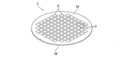
添付図面を参照して、本発明の一態様に係る実施形態について説明する。まず、本実施形態に係るウェーハの加工方法で加工されるウェーハについて説明する。図1は、ウェーハ1を模式的に示す斜視図である。 An embodiment according to one aspect of the present invention will be described with reference to the accompanying drawings. First, a wafer to be processed by the wafer processing method according to the present embodiment will be described. FIG. 1 is a perspective view schematically showing a
ウェーハ1は、例えば、Si(シリコン)、SiC(シリコンカーバイド)、GaN(ガリウムナイトライド)、GaAs(ヒ化ガリウム)、若しくは、その他の半導体等の材料、または、サファイア、ガラス、石英等の材料からなる略円板状の基板等である。該ガラスは、例えば、アルカリガラス、無アルカリガラス、ソーダ石灰ガラス、鉛ガラス、ホウケイ酸ガラス、石英ガラス等である。 The
ウェーハ1の表面1aは格子状に配列された複数の分割予定ライン3で区画される。また、ウェーハ1の表面1aの分割予定ライン3で区画された各領域にはICやLSI、LED等のデバイス5が形成される。本実施形態に係るウェーハ1の加工方法では、アブレーション加工により分割予定ライン3に沿った分割溝をウェーハ1に形成してウェーハ1を分割し、個々のデバイスチップを形成する。 The
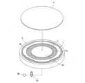
アブレーション加工が実施されるレーザー加工装置12(図8参照)にウェーハ1を搬入する前に、ウェーハ1と、ポリオレフィン系シートと、フレームと、が一体化され、フレームユニットが形成される。ウェーハ1は、フレームユニットの状態でレーザー加工装置に搬入され、加工される。形成された個々のデバイスチップはポリオレフィン系シートに支持される。その後、ポリオレフィン系シートを拡張することでデバイスチップ間の間隔を広げ、ピックアップ装置によりデバイスチップをピックアップする。 The
環状のフレーム7(図2等参照)は、例えば、金属等の材料で形成され、ウェーハ1の径よりも大きい径の開口7aを備える。フレームユニットを形成する際は、ウェーハ1は、フレーム7の開口7a内に位置付けられ、開口7aに収容される。 The annular frame 7 (see FIG. 2, etc.) is made of a material such as metal, and has an
ポリオレフィン系シート9(図3等参照)は、柔軟性を有する樹脂系シートであり、表裏面が平坦である。そして、ポリオレフィン系シート9は、フレーム7の外径よりも大きい径を有し、糊層を備えない。ポリオレフィン系シート9は、アルケンをモノマーとして合成されるポリマーのシートであり、例えば、ポリエチレンシート、ポリプロピレンシート、または、ポリスチレンシート等の可視光に対して透明または半透明なシートである。ただし、ポリオレフィン系シート9はこれに限定されず、不透明でもよい。 The polyolefin-based sheet 9 (see FIG. 3, etc.) is a flexible resin-based sheet having flat front and back surfaces. The
ポリオレフィン系シート9は、粘着性を備えないため室温ではウェーハ1及びフレーム7に貼着できない。しかしながら、ポリオレフィン系シート9は熱可塑性を有するため、所定の圧力を印加しながらウェーハ1及びフレーム7と接合させた状態で融点近傍の温度まで加熱すると、部分的に溶融してウェーハ1及びフレーム7に接着できる。そこで、本実施形態に係るウェーハ1の加工方法では以上のような熱圧着により、ウェーハ1と、フレーム7と、ポリオレフィン系シート9と、を一体化してフレームユニットを形成する。 Since the polyolefin-based
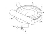
次に、本実施形態に係るウェーハ1の加工方法の各工程について説明する。まず、ウェーハ1と、ポリオレフィン系シート9と、フレーム7と、を一体化させる準備のために、ポリオレフィン系シート配設工程を実施する。図2は、チャックテーブル2の保持面2a上にウェーハ1及びフレーム7を位置付ける様子を模式的に示す斜視図である。図2に示す通り、ポリオレフィン系シート配設工程は、上部に保持面2aを備えるチャックテーブル2上で実施される。 Next, each step of the method for processing the
チャックテーブル2は、上部中央にフレーム7の外径よりも大きな径の多孔質部材を備える。該多孔質部材の上面は、チャックテーブル2の保持面2aとなる。チャックテーブル2は、図3に示す如く一端が該多孔質部材に通じた排気路を内部に有し、該排気路の他端側には吸引源2bが配設される。排気路には、連通状態と、切断状態と、を切り替える切り替え部2cが配設され、切り替え部2cが連通状態であると保持面2aに置かれた被保持物に吸引源2bにより生じた負圧が作用し、被保持物がチャックテーブル2に吸引保持される。 The chuck table 2 has a porous member having a diameter larger than the outer diameter of the
ポリオレフィン系シート配設工程では、まず、図2に示す通り、チャックテーブル2の保持面2a上にウェーハ1と、フレーム7と、を載せる。この際、ウェーハ1の表面1a側を下方に向け、フレーム7の開口7a内にウェーハ1を位置付ける。次に、ウェーハ1の裏面1bと、フレーム7の外周と、にポリオレフィン系シート9を配設する。図3は、ポリオレフィン系シート配設工程を模式的に示す斜視図である。図3に示す通り、ウェーハ1と、フレーム7と、を覆うように両者の上にポリオレフィン系シート9を配設する。 In the polyolefin sheet placement step, first, the
なお、ポリオレフィン系シート配設工程では、チャックテーブル2の保持面2aよりも大きな径のポリオレフィン系シート9が使用される。後に実施される一体化工程でチャックテーブル2による負圧をポリオレフィン系シート9に作用させる際に、保持面2aの全体がポリオレフィン系シート9により覆われていなければ、負圧が隙間から漏れてしまい、ポリオレフィン系シート9に適切に圧力を印加できないためである。 In the polyolefin sheet disposing process, the
本実施形態に係るウェーハ1の加工方法では、次に、ポリオレフィン系シート9を加熱し、熱圧着によりウェーハ1と該フレーム7とを該ポリオレフィン系シート9を介して一体化する一体化工程を実施する。図4は、一体化工程の一例を模式的に示す斜視図である。図4では、可視光に対して透明または半透明であるポリオレフィン系シート9を通して視認できるものを破線で示す。 In the method for processing the
一体化工程では、まず、チャックテーブル2の切り替え部2cを作動させて吸引源2bをチャックテーブル2の上部の多孔質部材に接続する連通状態とし、吸引源2bによる負圧をポリオレフィン系シート9に作用させる。すると、大気圧によりポリオレフィン系シート9がウェーハ1及びフレーム7に対して密着する。 In the integration step, first, the switching
次に、吸引源2bによりポリオレフィン系シート9を吸引しながらポリオレフィン系シート9を加熱して、熱圧着を実施する。ポリオレフィン系シート9の加熱は、例えば、図4に示す通り、チャックテーブル2の上方に配設されるヒートガン4により実施される。 Next, the polyolefin-based
ヒートガン4は、電熱線等の加熱手段と、ファン等の送風機構と、を内部に備え、空気を加熱し噴射できる。負圧をポリオレフィン系シート9に作用させながらヒートガン4によりポリオレフィン系シート9に上面から熱風4aを供給し、ポリオレフィン系シート9を所定の温度に加熱すると、ポリオレフィン系シート9がウェーハ1及びフレーム7に熱圧着される。 The heat gun 4 includes a heating means such as a heating wire and a blowing mechanism such as a fan, and can heat and jet air. While applying a negative pressure to the
また、ポリオレフィン系シート9の加熱は、他の方法により実施されてもよく、例えば、所定の温度に加熱された部材でウェーハ1及びフレーム7を上方から押圧することで実施される。図5は一体化工程の他の一例を模式的に示す斜視図である。図5では、可視光に対して透明または半透明であるポリオレフィン系シート9を通して視認できるものを破線で示す。 Moreover, the heating of the polyolefin-based
図5に示す一体化工程では、例えば、内部に熱源を備えるヒートローラー6を使用する。図5に示す一体化工程においても、まず、吸引源2bによる負圧をポリオレフィン系シート9に作用させ、大気圧によりポリオレフィン系シート9をウェーハ1及びフレーム7に密着させる。 In the integration step shown in FIG. 5, for example, a
その後、ヒートローラー6を所定の温度に加熱して、チャックテーブル2の保持面2aの一端に該ヒートローラー6を載せる。そして、ヒートローラー6を回転させ、該一端から他端にまでチャックテーブル2上でヒートローラー6を転がす。すると、ポリオレフィン系シート9がウェーハ1及びフレーム7に熱圧着される。この際、ヒートローラー6によりポリオレフィン系シート9を押し下げる方向に力を印加すると、大気圧より大きい圧力で熱圧着が実施される。尚、ヒートローラー6の表面をフッ素樹脂で被覆することが好ましい。 After that, the
また、内部に熱源を備え、平たい底板を有するアイロン状の押圧部材をヒートローラー6に代えて使用してポリオレフィン系シート9の熱圧着を実施してもよい。この場合、該押圧部材を所定の温度に加熱して熱板とし、チャックテーブル2に保持されたポリオレフィン系シート9を該押圧部材で上方から押圧する。 Alternatively, the
ポリオレフィン系シート9の加熱は、さらに他の方法により実施されてもよい。図6は、一体化工程のさらに他の一例を模式的に示す斜視図である。図6では、可視光に対して透明または半透明であるポリオレフィン系シート9を通して視認できるものを破線で示す。図6に示す一体化工程では、チャックテーブル2の上方に配された赤外線ランプ8を使用してポリオレフィン系シート9を加熱する。赤外線ランプ8は、少なくともポリオレフィン系シート9の材料が吸収性を有する波長の赤外線8aを照射可能である。 Heating of the polyolefin-based
図6に示す一体化工程においても、まず、吸引源2bによる負圧をポリオレフィン系シート9に作用させ、ポリオレフィン系シート9をウェーハ1及びフレーム7に密着させる。次に、赤外線ランプ8を作動させて、ポリオレフィン系シート9に赤外線8aを照射してポリオレフィン系シート9を加熱する。すると、ポリオレフィン系シート9がウェーハ1及びフレーム7に熱圧着される。 Also in the integration step shown in FIG. 6 , first, a negative pressure is applied to the polyolefin-based
いずれかの方法によりポリオレフィン系シート9がその融点近傍の温度にまで加熱されると、ポリオレフィン系シート9がウェーハ1及びフレーム7に熱圧着される。ポリオレフィン系シート9を熱圧着した後は、切り替え部2cを作動させてチャックテーブル2の多孔質部材と、吸引源2bと、の連通状態を解除し、チャックテーブル2による吸着を解除する。 When the polyolefin-based
次に、フレーム7の外周からはみ出したポリオレフィン系シート9を切断して除去する。図7(A)は、ポリオレフィン系シート9を切断する様子を模式的に示す斜視図である。切断には、図7(A)に示す通り、円環状のカッター10が使用される。該カッター10は、貫通孔を備え、該貫通孔に突き通された回転軸の回りに回転可能である。 Next, the polyolefin-based
まず、円環状のカッター10をフレーム7の上方に位置付ける。このとき、カッター10の回転軸をチャックテーブル2の径方向に合わせる。次に、カッター10を下降させてフレーム7と、カッター10と、でポリオレフィン系シート9を挟み込み、ポリオレフィン系シート9を切断する。すると、ポリオレフィン系シート9に切断痕9aが形成される。 First, the
さらに、カッター10をフレーム7に沿ってフレーム7の開口7aの周りを一周させ、切断痕9aによりポリオレフィン系シート9の所定の領域を囲む。そして、ポリオレフィン系シート9の該領域を残すように切断痕9aの外周側の領域のポリオレフィン系シート9を除去する。すると、フレーム7の外周からはみ出した領域を含めポリオレフィン系シート9の不要な部分を除去できる。 Further, the
なお、ポリオレフィン系シートの切断には超音波カッターを使用してもよく、上述の円環状のカッター10を超音波帯の周波数で振動させる振動源を該カッター10に接続してもよい。また、ポリオレフィン系シート9を切断する際は、切断を容易にするために該ポリオレフィン系シート9を冷却して硬化させてもよい。以上により、ウェーハ1とフレーム7とがポリオレフィン系シート9を介して一体化されたフレームユニット11が形成される。図7(B)は、形成されたフレームユニット11を模式的に示す斜視図である。 An ultrasonic cutter may be used for cutting the polyolefin sheet, and a vibration source for vibrating the
なお、熱圧着を実施する際にポリオレフィン系シート9は、好ましくは、その融点以下の温度に加熱される。加熱温度が融点を超えると、ポリオレフィン系シート9が溶解してシートの形状を維持できなくなる場合があるためである。また、ポリオレフィン系シート9は、好ましくは、その軟化点以上の温度に加熱される。加熱温度が軟化点に達していなければ熱圧着を適切に実施できないためである。すなわち、ポリオレフィン系シート9は、その軟化点以上でかつその融点以下の温度に加熱されるのが好ましい。 It should be noted that the
さらに、一部のポリオレフィン系シート9は、明確な軟化点を有しない場合もある。そこで、熱圧着を実施する際にポリオレフィン系シート9は、好ましくは、その融点よりも20℃低い温度以上でかつその融点以下の温度に加熱される。 Furthermore, some polyolefin-based
また、ポリオレフィン系シート9がポリエチレンシートである場合、加熱温度は120℃~140℃とされるのが好ましい。また、該ポリオレフィン系シート9がポリプロピレンシートである場合、加熱温度は160℃~180℃とされるのが好ましい。さらに、ポリオレフィン系シート9がポリスチレンシートである場合、加熱温度は220℃~240℃とされるのが好ましい。 Further, when the
ここで、加熱温度とは、一体化工程を実施する際のポリオレフィン系シート9の温度をいう。例えば、ヒートガン4、ヒートローラー6、赤外線ランプ8等の熱源では出力温度を設定できる機種が実用に供されているが、該熱源を使用してポリオレフィン系シート9を加熱しても、ポリオレフィン系シート9の温度が設定された該出力温度にまで達しない場合もある。そこで、ポリオレフィン系シート9を所定の温度に加熱するために、熱源の出力温度をポリオレフィン系シート9の融点よりも高く設定してもよい。 Here, the heating temperature refers to the temperature of the polyolefin-based
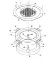
次に、本実施形態に係るウェーハの加工方法では、フレームユニット11の状態となったウェーハ1をアブレーション加工して、分割予定ライン3に沿った分割溝を形成して該ウェーハ1を分割する分割工程を実施する。分割工程は、例えば、図8に示すレーザー加工装置で実施される。図8は、分割工程を模式的に示す斜視図である。 Next, in the wafer processing method according to the present embodiment, the
レーザー加工装置12は、ウェーハ1をアブレーション加工するレーザー加工ユニット14と、ウェーハ1を保持するチャックテーブル(不図示)と、を備える。レーザー加工ユニット14は、レーザーを発振できるレーザー発振器(不図示)を備え、ウェーハ1に対して吸収性を有する波長の(ウェーハ1が吸収できる波長の)レーザービーム16を出射できる。該チャックテーブルは、上面に平行な方向に沿って移動(加工送り)できる。 The
レーザー加工ユニット14は、該レーザー発振器から出射されたレーザービーム16を該チャックテーブルに保持されたウェーハ1に照射する。レーザー加工ユニット14が備える加工ヘッド14aは、レーザービーム16をウェーハ1の所定の高さ位置に集光する機構を有する。 A
ウェーハ1をアブレーション加工する際には、チャックテーブルの上にフレームユニット11を載せ、ポリオレフィン系シート9を介してチャックテーブルにウェーハ1を保持させる。そして、チャックテーブルを回転させウェーハ1の分割予定ライン3をレーザー加工装置12の加工送り方向に合わせる。また、分割予定ライン3の延長線の上方に加工ヘッド14aが配設されるように、チャックテーブル及びレーザー加工ユニット14の相対位置を調整する。 When the
次に、レーザー加工ユニット14からウェーハ1にレーザービーム16を照射しながらチャックテーブルと、レーザー加工ユニット14と、をチャックテーブルの上面に平行な加工送り方向に沿って相対移動させる。すると、分割予定ライン3に沿ってレーザービーム16がウェーハ1に照射され、アブレーションにより分割予定ライン3に沿った分割溝3aがウェーハ1に形成される。 Next, while irradiating the
分割工程におけるレーザービーム16の照射条件は、例えば、以下のように設定される。ただし、レーザービーム16の照射条件は、これに限定されない。
波長 :355nm
繰り返し周波数:50kHz
平均出力 :5W
送り速度 :200mm/秒The irradiation conditions of the
Wavelength: 355nm
Repetition frequency: 50kHz
Average output: 5W
Feeding speed: 200mm/sec
一つの分割予定ライン3に沿ってアブレーション加工を実施した後、チャックテーブル及びレーザー加工ユニット14を加工送り方向とは垂直な割り出し送り方向に相対的に移動させ、他の分割予定ライン3に沿って同様にウェーハ1のアブレーション加工を実施する。一つの方向に沿った全ての分割予定ライン3に沿って分割溝3aを形成した後、チャックテーブルを保持面に垂直な軸の回りに回転させ、他の方向に沿った分割予定ライン3に沿って同様にウェーハ1をアブレーション加工する。 After performing ablation along one of the planned dividing lines 3, the chuck table and the
ウェーハ1のすべての分割予定ライン3に沿ってウェーハ1がアブレーション加工されると、分割工程が完了する。分割工程が完了し、すべての分割予定ライン3に沿って表面1aから裏面1bに至る分割溝3aがウェーハ1に形成されると、ウェーハ1が分割され個々のデバイスチップが形成される。 When the
レーザー加工ユニット14によりウェーハ1にアブレーション加工を実施すると、レーザービーム16の被照射箇所からウェーハ1に由来する加工屑が発生し、該加工屑が該被照射箇所の周囲に飛散してウェーハ1の表面1aに付着する。ウェーハ1にアブレーション加工を実施した後、ウェーハ1の表面1aを後述の洗浄ユニットにより洗浄しても、付着した加工屑を完全に除去するのは容易ではない。ウェーハ1から形成されるデバイスチップに該加工屑が残存すると、デバイスチップの品質が低下する。 When the
そこで、レーザー加工装置12でアブレーション加工されるウェーハ1の表面1aには、予め、ウェーハ1の表面1aを保護する保護膜として機能する水溶性の液状樹脂が塗布されていてもよい。該液状樹脂がウェーハ1の表面1aに塗布されていると、アブレーション加工を実施する際に飛散する加工屑が該液状樹脂の上面に付着するため、加工屑はウェーハ1の表面1aに直接付着しない。そして、次に説明する洗浄ユニットにより、該加工屑は該液状樹脂ごと除去される。 Therefore, the
レーザー加工装置12は、洗浄ユニット(不図示)を備えてもよい。この場合、レーザー加工ユニット14によりアブレーション加工されたウェーハ1は、該洗浄ユニットに搬送され、該洗浄ユニットにより洗浄される。例えば、洗浄ユニットはフレームユニット11を保持する洗浄テーブルと、フレームユニット11の上方を往復移動できる洗浄水供給ノズルと、を備える。 The
洗浄テーブルを保持面に垂直な軸の回りに回転させ、洗浄水供給ノズルから純水等の洗浄液をウェーハ1に供給しながら、洗浄水供給ノズルを該保持面の中央の上方を通る経路で水平方向に往復移動させると、ウェーハ1の表面1a側を洗浄できる。 The cleaning table is rotated around an axis perpendicular to the holding surface, and while a cleaning liquid such as pure water is supplied from the cleaning water supply nozzle to the
本実施形態に係るウェーハ1の加工方法では、次に、ポリオレフィン系シート9から個々の該デバイスチップをピックアップするピックアップ工程を実施する。ピックアップ工程では、図9下部に示すピックアップ装置18を使用する。図9は、ピックアップ装置18へのフレームユニット11の搬入を模式的に示す斜視図である。 In the method for processing the
ピックアップ装置18は、ウェーハ1の径よりも大きい径を有する円筒状のドラム20と、フレーム支持台26を含むフレーム保持ユニット22と、を備える。フレーム保持ユニット22のフレーム支持台26は、該ドラム20の径よりも大きい径の開口を備え、該ドラム20の上端部と同様の高さに配設され、該ドラム20の上端部を外周側から囲む。 The
フレーム支持台26の外周側には、クランプ24が配設される。フレーム支持台26の上にフレームユニット11を載せ、クランプ24によりフレームユニット11のフレーム7を把持させると、フレームユニット11がフレーム支持台26に固定される。 A
フレーム支持台26は、鉛直方向に沿って伸長する複数のロッド28により支持され、各ロッド28の下端部には、該ロッド28を昇降させるエアシリンダ30が配設される。複数のエアシリンダ30は、円板状のベース32に支持される。各エアシリンダ30を作動させると、フレーム支持台26がドラム20に対して引き下げられる。 The
ドラム20の内部には、ポリオレフィン系シート9に支持されたデバイスチップを下方から突き上げる突き上げ機構34が配設される。突き上げ機構34は、例えば、チタン酸ジルコン酸鉛(PZT)、チタン酸バリウム、チタン酸鉛等の圧電セラミックス、又は水晶振動子等から構成される超音波振動子34aを上端に備える。また、ドラム20の上方には、デバイスチップを吸引保持できるコレット36(図10(B)参照)が配設される。突き上げ機構34及びコレット36は、フレーム支持台26の上面に沿った水平方向に移動可能である。また、コレット36は、切り替え部36b(図10(B)参照)を介して吸引源36a(図10(B)参照)に接続される。 A push-up
ピックアップ工程では、まず、ピックアップ装置18のドラム20の上端の高さと、フレーム支持台26の上面の高さと、が一致するように、エアシリンダ30を作動させてフレーム支持台26の高さを調節する。次に、レーザー加工装置12から搬出されたフレームユニット11をピックアップ装置18のドラム20及びフレーム支持台26の上に載せる。 In the pick-up process, first, the
その後、クランプ24によりフレーム支持台26の上にフレームユニット11のフレーム7を固定する。図10(A)は、フレーム支持台26の上に固定されたフレームユニット11を模式的に示す断面図である。ウェーハ1には、分割工程により分割溝3aが形成され分割されている。 After that, the
次に、エアシリンダ30を作動させてフレーム保持ユニット22のフレーム支持台26をドラム20に対して引き下げる。すると、図10(B)に示す通り、ポリオレフィン系シート9が外周方向に拡張される。図10(B)は、ピックアップ工程を模式的に示す断面図である。 Next, the
ポリオレフィン系シート9が外周方向に拡張されると、ポリオレフィン系シート9に支持された各デバイスチップ1cの間隔が広げられる。すると、デバイスチップ1c同士が接触しにくくなり、個々のデバイスチップ1cのピックアップが容易となる。そして、ピックアップの対象となるデバイスチップ1cを決め、該デバイスチップ1cの下方に突き上げ機構34を移動させ、該デバイスチップ1cの上方にコレット36を移動させる。 When the polyolefin-based
その後、超音波振動子34aを作動させて超音波帯域の周波数の振動を生じさせ、超音波振動子34aをポリオレフィン系シート9の該デバイスチップ1cに対応する領域に接触させて該領域に超音波を付与する。さらに、突き上げ機構34を作動させてポリオレフィン系シート9側から該デバイスチップ1cを突き上げる。そして、切り替え部36bを作動させてコレット36を吸引源36aに連通させる。すると、コレット36により該デバイスチップ1cが吸引保持され、デバイスチップ1cがポリオレフィン系シート9からピックアップされる。ピックアップされた個々のデバイスチップ1cは、その後、所定の配線基板等に実装されて使用される。 After that, the
なお、ポリオレフィン系シート9の該領域に超音波振動子34aにより超音波を付与すると、ポリオレフィン系シート9の剥離が容易となる。そのため、ポリオレフィン系シート9からの剥離時にデバイスチップにかかる負荷が軽減される。 If ultrasonic waves are applied to the region of the
例えば、粘着テープを使用してフレームユニット11を形成する場合、分割工程においてレーザービーム16の照射により生じる熱が該粘着テープに伝わり、粘着テープの糊層が溶融してデバイスチップの裏面側に固着する。そして、糊層の付着によるデバイスチップの品質の低下が問題となる。 For example, when the
これに対して、本実施形態に係るウェーハの加工方法によると、熱圧着により糊層を備えないポリオレフィン系シートを用いたフレームユニットの形成が可能となるため、糊層を備えた粘着テープが不要である。結果として裏面側への糊層の付着によるデバイスチップの品質低下が生じない。 In contrast, according to the wafer processing method according to the present embodiment, it is possible to form a frame unit using a polyolefin-based sheet that does not have an adhesive layer by thermocompression bonding, so adhesive tape with an adhesive layer is unnecessary. is. As a result, the quality of the device chip does not deteriorate due to adhesion of the glue layer to the back surface.
なお、本発明は上記実施形態の記載に限定されず、種々変更して実施可能である。例えば、上記実施形態では、ポリオレフィン系シート9が、例えば、ポリエチレンシート、ポリプロピレンシート、または、ポリスチレンシートである場合について説明したが、本発明の一態様はこれに限定されない。例えば、ポリオレフィン系シートは、他の材料が使用されてもよく、プロピレンとエチレンとのコポリマーや、オレフィン系エラストマー等でもよい。 It should be noted that the present invention is not limited to the description of the above embodiments, and can be implemented with various modifications. For example, in the above embodiment, the
その他、上記実施形態に係る構造、方法等は、本発明の目的の範囲を逸脱しない限りにおいて適宜変更して実施できる。 In addition, the structures, methods, and the like according to the above-described embodiments can be modified as appropriate without departing from the scope of the present invention.
1 ウェーハ
1a 表面
1b 裏面
3 分割予定ライン
3a 分割溝
5 デバイス
7 フレーム
7a 開口
9 ポリオレフィン系シート
9a 切断痕
11 フレームユニット
2 チャックテーブル
2a 保持面
2b,36a 吸引源
2c,36b 切り替え部
4 ヒートガン
4a 熱風
6 ヒートローラー
8 赤外線ランプ
8a 赤外線
10 カッター
12 レーザー加工装置
14 レーザー加工ユニット
14a 加工ヘッド
16 レーザービーム
18 ピックアップ装置
20 ドラム
22 フレーム保持ユニット
24 クランプ
26 フレーム支持台
28 ロッド
30 エアシリンダ
32 ベース
34 突き上げ機構
34a 超音波振動子
36 コレットREFERENCE SIGNS
Claims (9)
Translated fromJapaneseウェーハを収容する開口を有するフレームの該開口内にウェーハを位置付け、該ウェーハの裏面と該フレームの外周とに糊層を備えないポリオレフィン系シートを配設するポリオレフィン系シート配設工程と、
該ポリオレフィン系シートを加熱し熱圧着により該ウェーハと該フレームとを該ポリオレフィン系シートを介して一体化する一体化工程と、
該ウェーハに対して吸収性を有する波長のレーザービームを該分割予定ラインに沿って該ウェーハに照射し、分割溝を形成して該ウェーハを個々のデバイスチップに分割する分割工程と、
該ポリオレフィン系シートの各デバイスチップに対応する個々の領域において、該ポリオレフィン系シートに超音波を付与し、該ポリオレフィン系シート側から該デバイスチップを突き上げ、該ポリオレフィン系シートから該デバイスチップをピックアップするピックアップ工程と、
を備えることを特徴とするウェーハの加工方法。A wafer processing method for dividing a wafer in which a plurality of devices are formed in respective regions of a surface partitioned by dividing lines into individual device chips,
a polyolefin-based sheet disposing step of positioning a wafer in an opening of a frame having an opening for accommodating the wafer, and disposing a polyolefin-based sheethaving no adhesive layer on the back surface of the wafer and the outer periphery of the frame;
an integration step of heating the polyolefin-based sheet and integrating the wafer and the frame through the polyolefin-based sheet by thermocompression bonding;
a dividing step of irradiating the wafer with a laser beam having a wavelength that is absorptive to the wafer along the dividing lines to form dividing grooves to divide the wafer into individual device chips;
Ultrasonic waves are applied to the polyolefin-based sheet in individual regions corresponding to each device chip of the polyolefin-based sheet, the device chip is pushed up from the polyolefin-based sheet side, and the device chip is picked up from the polyolefin-based sheet. a pick-up process;
A wafer processing method comprising:
Priority Applications (8)
| Application Number | Priority Date | Filing Date | Title |
|---|---|---|---|
| JP2019025260AJP7282452B2 (en) | 2019-02-15 | 2019-02-15 | Wafer processing method |
| MYPI2020000264AMY195428A (en) | 2019-02-15 | 2020-01-16 | Wafer Processing Method |
| SG10202000576QASG10202000576QA (en) | 2019-02-15 | 2020-01-21 | Wafer processing method |
| US16/774,689US11004744B2 (en) | 2019-02-15 | 2020-01-28 | Wafer processing method for dividing a wafer along predefined division lines |
| KR1020200014303AKR20200099979A (en) | 2019-02-15 | 2020-02-06 | Wafer processing method |
| CN202010084444.3ACN111584428A (en) | 2019-02-15 | 2020-02-10 | Method for processing wafer |
| TW109104250ATWI840505B (en) | 2019-02-15 | 2020-02-11 | Wafer processing method |
| DE102020201866.9ADE102020201866B4 (en) | 2019-02-15 | 2020-02-14 | Wafer processing methods |
Applications Claiming Priority (1)
| Application Number | Priority Date | Filing Date | Title |
|---|---|---|---|
| JP2019025260AJP7282452B2 (en) | 2019-02-15 | 2019-02-15 | Wafer processing method |
Publications (2)
| Publication Number | Publication Date |
|---|---|
| JP2020136370A JP2020136370A (en) | 2020-08-31 |
| JP7282452B2true JP7282452B2 (en) | 2023-05-29 |
Family
ID=71844038
Family Applications (1)
| Application Number | Title | Priority Date | Filing Date |
|---|---|---|---|
| JP2019025260AActiveJP7282452B2 (en) | 2019-02-15 | 2019-02-15 | Wafer processing method |
Country Status (8)
| Country | Link |
|---|---|
| US (1) | US11004744B2 (en) |
| JP (1) | JP7282452B2 (en) |
| KR (1) | KR20200099979A (en) |
| CN (1) | CN111584428A (en) |
| DE (1) | DE102020201866B4 (en) |
| MY (1) | MY195428A (en) |
| SG (1) | SG10202000576QA (en) |
| TW (1) | TWI840505B (en) |
Families Citing this family (5)
| Publication number | Priority date | Publication date | Assignee | Title |
|---|---|---|---|---|
| JP7140626B2 (en)* | 2018-10-10 | 2022-09-21 | 株式会社ディスコ | Ring frame holding mechanism |
| JP7430515B2 (en)* | 2019-11-06 | 2024-02-13 | 株式会社ディスコ | Wafer processing method |
| JP2023047440A (en) | 2021-09-27 | 2023-04-06 | 株式会社ディスコ | Processing method for plate-shaped object |
| JP7737881B2 (en)* | 2021-12-01 | 2025-09-11 | 株式会社ディスコ | Workpiece processing method and laser processing device |
| WO2024024164A1 (en)* | 2022-07-26 | 2024-02-01 | パナソニックIpマネジメント株式会社 | Pickup system and pickup method |
Citations (7)
| Publication number | Priority date | Publication date | Assignee | Title |
|---|---|---|---|---|
| JP2003264203A (en) | 2002-03-11 | 2003-09-19 | Hitachi Ltd | Method for manufacturing semiconductor device |
| JP2004119975A (en) | 1995-12-04 | 2004-04-15 | Renesas Technology Corp | Method of manufacturing ic card |
| JP2007165636A (en) | 2005-12-14 | 2007-06-28 | Nippon Zeon Co Ltd | Manufacturing method of semiconductor device |
| JP2011187537A (en) | 2010-03-05 | 2011-09-22 | Lintec Corp | Apparatus and method for sticking sheet |
| WO2016151911A1 (en) | 2015-03-23 | 2016-09-29 | リンテック株式会社 | Semiconductor processing sheet and method for manufacturing semiconductor device |
| JP2018085434A (en) | 2016-11-24 | 2018-05-31 | 株式会社ディスコ | Method for processing wafer |
| JP2018166177A (en) | 2017-03-28 | 2018-10-25 | 株式会社ディスコ | Wafer processing system |
Family Cites Families (21)
| Publication number | Priority date | Publication date | Assignee | Title |
|---|---|---|---|---|
| JP3076179B2 (en) | 1993-07-26 | 2000-08-14 | 株式会社ディスコ | Dicing equipment |
| JPH10305420A (en) | 1997-03-04 | 1998-11-17 | Ngk Insulators Ltd | Processing method of base material composed of oxide single crystal and method of manufacturing functional device |
| JP3076179U (en) | 2000-09-07 | 2001-03-30 | 和雄 落合 | Cup type bottle cap |
| JP2003152056A (en) | 2001-11-08 | 2003-05-23 | Sony Corp | Semiconductor element holder and method of manufacturing the same |
| TWI225279B (en)* | 2002-03-11 | 2004-12-11 | Hitachi Ltd | Semiconductor device and its manufacturing method |
| TWI310230B (en)* | 2003-01-22 | 2009-05-21 | Lintec Corp | Adhesive sheet, method for protecting surface of semiconductor wafer and method for processing work |
| JP4647228B2 (en)* | 2004-04-01 | 2011-03-09 | 株式会社ディスコ | Wafer processing method |
| FI20060256A7 (en)* | 2006-03-17 | 2006-03-20 | Imbera Electronics Oy | Circuit board manufacturing and circuit board containing the component |
| JP5054933B2 (en)* | 2006-05-23 | 2012-10-24 | ルネサスエレクトロニクス株式会社 | Manufacturing method of semiconductor device |
| JP2008117943A (en)* | 2006-11-06 | 2008-05-22 | Nitto Denko Corp | Adhesive sheet for water jet laser dicing |
| US8507359B2 (en)* | 2009-12-02 | 2013-08-13 | Sharp Kabushiki Kaisha | Semiconductor device, process for producing same, and display device |
| JP5801046B2 (en)* | 2010-12-06 | 2015-10-28 | 株式会社ディスコ | Processing method of plate |
| US9559004B2 (en)* | 2011-05-12 | 2017-01-31 | STATS ChipPAC Pte. Ltd. | Semiconductor device and method of singulating thin semiconductor wafer on carrier along modified region within non-active region formed by irradiating energy |
| WO2013047674A1 (en)* | 2011-09-30 | 2013-04-04 | リンテック株式会社 | Dicing sheet with protective film forming layer and chip fabrication method |
| US9230888B2 (en)* | 2013-02-11 | 2016-01-05 | Henkel IP & Holding GmbH | Wafer back side coating as dicing tape adhesive |
| JP6425435B2 (en)* | 2014-07-01 | 2018-11-21 | 株式会社ディスコ | Tip spacing maintenance device |
| JP5862733B1 (en)* | 2014-09-08 | 2016-02-16 | 富士ゼロックス株式会社 | Manufacturing method of semiconductor piece |
| US10269641B2 (en)* | 2016-11-30 | 2019-04-23 | Plasma-Therm Llc | Method and apparatus for plasma dicing a semi-conductor wafer |
| SG11201906797WA (en)* | 2017-02-24 | 2019-08-27 | Furukawa Electric Co Ltd | Mask-integrated surface protective tape, and method of producing a semiconductor chip using the same |
| JP2019192717A (en) | 2018-04-20 | 2019-10-31 | 株式会社ディスコ | Method of processing wafer |
| JP7154809B2 (en) | 2018-04-20 | 2022-10-18 | 株式会社ディスコ | Wafer processing method |
- 2019
- 2019-02-15JPJP2019025260Apatent/JP7282452B2/enactiveActive
- 2020
- 2020-01-16MYMYPI2020000264Apatent/MY195428A/enunknown
- 2020-01-21SGSG10202000576QApatent/SG10202000576QA/enunknown
- 2020-01-28USUS16/774,689patent/US11004744B2/enactiveActive
- 2020-02-06KRKR1020200014303Apatent/KR20200099979A/enactivePending
- 2020-02-10CNCN202010084444.3Apatent/CN111584428A/enactivePending
- 2020-02-11TWTW109104250Apatent/TWI840505B/enactive
- 2020-02-14DEDE102020201866.9Apatent/DE102020201866B4/enactiveActive
Patent Citations (7)
| Publication number | Priority date | Publication date | Assignee | Title |
|---|---|---|---|---|
| JP2004119975A (en) | 1995-12-04 | 2004-04-15 | Renesas Technology Corp | Method of manufacturing ic card |
| JP2003264203A (en) | 2002-03-11 | 2003-09-19 | Hitachi Ltd | Method for manufacturing semiconductor device |
| JP2007165636A (en) | 2005-12-14 | 2007-06-28 | Nippon Zeon Co Ltd | Manufacturing method of semiconductor device |
| JP2011187537A (en) | 2010-03-05 | 2011-09-22 | Lintec Corp | Apparatus and method for sticking sheet |
| WO2016151911A1 (en) | 2015-03-23 | 2016-09-29 | リンテック株式会社 | Semiconductor processing sheet and method for manufacturing semiconductor device |
| JP2018085434A (en) | 2016-11-24 | 2018-05-31 | 株式会社ディスコ | Method for processing wafer |
| JP2018166177A (en) | 2017-03-28 | 2018-10-25 | 株式会社ディスコ | Wafer processing system |
Also Published As
| Publication number | Publication date |
|---|---|
| CN111584428A (en) | 2020-08-25 |
| JP2020136370A (en) | 2020-08-31 |
| TW202032651A (en) | 2020-09-01 |
| US20200266102A1 (en) | 2020-08-20 |
| DE102020201866A1 (en) | 2020-08-20 |
| TWI840505B (en) | 2024-05-01 |
| MY195428A (en) | 2023-01-20 |
| SG10202000576QA (en) | 2020-09-29 |
| US11004744B2 (en) | 2021-05-11 |
| KR20200099979A (en) | 2020-08-25 |
| DE102020201866B4 (en) | 2024-05-02 |
Similar Documents
| Publication | Publication Date | Title |
|---|---|---|
| JP7281873B2 (en) | Wafer processing method | |
| JP7282452B2 (en) | Wafer processing method | |
| JP7154686B2 (en) | Wafer processing method | |
| JP7224719B2 (en) | Wafer processing method | |
| JP7246825B2 (en) | Wafer processing method | |
| CN111063607B (en) | Wafer processing method | |
| JP7282453B2 (en) | Wafer processing method | |
| JP7286245B2 (en) | Wafer processing method | |
| JP7199786B2 (en) | Wafer processing method | |
| CN111146115B (en) | Wafer processing method | |
| JP7229636B2 (en) | Wafer processing method | |
| JP7171134B2 (en) | Wafer processing method | |
| JP7251898B2 (en) | Wafer processing method | |
| JP7330615B2 (en) | Wafer processing method | |
| JP7282455B2 (en) | Wafer processing method | |
| JP7175560B2 (en) | Wafer processing method | |
| JP7166720B2 (en) | Wafer processing method | |
| JP7166719B2 (en) | Wafer processing method | |
| JP2020136378A (en) | Wafer processing method | |
| JP2020136405A (en) | Wafer processing method | |
| JP7175566B2 (en) | Wafer processing method | |
| JP7175567B2 (en) | Wafer processing method | |
| JP7171136B2 (en) | Wafer processing method | |
| JP7171135B2 (en) | Wafer processing method | |
| JP7286241B2 (en) | Wafer processing method |
Legal Events
| Date | Code | Title | Description |
|---|---|---|---|
| A621 | Written request for application examination | Free format text:JAPANESE INTERMEDIATE CODE: A621 Effective date:20211210 | |
| A977 | Report on retrieval | Free format text:JAPANESE INTERMEDIATE CODE: A971007 Effective date:20221208 | |
| A131 | Notification of reasons for refusal | Free format text:JAPANESE INTERMEDIATE CODE: A131 Effective date:20221213 | |
| A521 | Request for written amendment filed | Free format text:JAPANESE INTERMEDIATE CODE: A523 Effective date:20230208 | |
| TRDD | Decision of grant or rejection written | ||
| A01 | Written decision to grant a patent or to grant a registration (utility model) | Free format text:JAPANESE INTERMEDIATE CODE: A01 Effective date:20230516 | |
| A61 | First payment of annual fees (during grant procedure) | Free format text:JAPANESE INTERMEDIATE CODE: A61 Effective date:20230516 | |
| R150 | Certificate of patent or registration of utility model | Ref document number:7282452 Country of ref document:JP Free format text:JAPANESE INTERMEDIATE CODE: R150 |