JP7266565B2 - How to make a transistor - Google Patents
How to make a transistorDownload PDFInfo
- Publication number
- JP7266565B2 JP7266565B2JP2020179922AJP2020179922AJP7266565B2JP 7266565 B2JP7266565 B2JP 7266565B2JP 2020179922 AJP2020179922 AJP 2020179922AJP 2020179922 AJP2020179922 AJP 2020179922AJP 7266565 B2JP7266565 B2JP 7266565B2
- Authority
- JP
- Japan
- Prior art keywords
- film
- oxide semiconductor
- oxide
- transistor
- insulating film
- Prior art date
- Legal status (The legal status is an assumption and is not a legal conclusion. Google has not performed a legal analysis and makes no representation as to the accuracy of the status listed.)
- Active
Links
Images


Classifications
- H—ELECTRICITY
- H10—SEMICONDUCTOR DEVICES; ELECTRIC SOLID-STATE DEVICES NOT OTHERWISE PROVIDED FOR
- H10D—INORGANIC ELECTRIC SEMICONDUCTOR DEVICES
- H10D30/00—Field-effect transistors [FET]
- H10D30/60—Insulated-gate field-effect transistors [IGFET]
- H10D30/67—Thin-film transistors [TFT]
- H10D30/674—Thin-film transistors [TFT] characterised by the active materials
- H10D30/6755—Oxide semiconductors, e.g. zinc oxide, copper aluminium oxide or cadmium stannate
- H—ELECTRICITY
- H10—SEMICONDUCTOR DEVICES; ELECTRIC SOLID-STATE DEVICES NOT OTHERWISE PROVIDED FOR
- H10D—INORGANIC ELECTRIC SEMICONDUCTOR DEVICES
- H10D30/00—Field-effect transistors [FET]
- H10D30/60—Insulated-gate field-effect transistors [IGFET]
- H10D30/67—Thin-film transistors [TFT]
- H10D30/6704—Thin-film transistors [TFT] having supplementary regions or layers in the thin films or in the insulated bulk substrates for controlling properties of the device
- H10D30/6713—Thin-film transistors [TFT] having supplementary regions or layers in the thin films or in the insulated bulk substrates for controlling properties of the device characterised by the properties of the source or drain regions, e.g. compositions or sectional shapes
- H—ELECTRICITY
- H10—SEMICONDUCTOR DEVICES; ELECTRIC SOLID-STATE DEVICES NOT OTHERWISE PROVIDED FOR
- H10D—INORGANIC ELECTRIC SEMICONDUCTOR DEVICES
- H10D62/00—Semiconductor bodies, or regions thereof, of devices having potential barriers
- H10D62/40—Crystalline structures
- H—ELECTRICITY
- H10—SEMICONDUCTOR DEVICES; ELECTRIC SOLID-STATE DEVICES NOT OTHERWISE PROVIDED FOR
- H10D—INORGANIC ELECTRIC SEMICONDUCTOR DEVICES
- H10D62/00—Semiconductor bodies, or regions thereof, of devices having potential barriers
- H10D62/80—Semiconductor bodies, or regions thereof, of devices having potential barriers characterised by the materials
- H10D62/85—Semiconductor bodies, or regions thereof, of devices having potential barriers characterised by the materials being Group III-V materials, e.g. GaAs
- H—ELECTRICITY
- H10—SEMICONDUCTOR DEVICES; ELECTRIC SOLID-STATE DEVICES NOT OTHERWISE PROVIDED FOR
- H10D—INORGANIC ELECTRIC SEMICONDUCTOR DEVICES
- H10D62/00—Semiconductor bodies, or regions thereof, of devices having potential barriers
- H10D62/80—Semiconductor bodies, or regions thereof, of devices having potential barriers characterised by the materials
- H10D62/86—Semiconductor bodies, or regions thereof, of devices having potential barriers characterised by the materials being Group II-VI materials, e.g. ZnO
- H—ELECTRICITY
- H10—SEMICONDUCTOR DEVICES; ELECTRIC SOLID-STATE DEVICES NOT OTHERWISE PROVIDED FOR
- H10D—INORGANIC ELECTRIC SEMICONDUCTOR DEVICES
- H10D86/00—Integrated devices formed in or on insulating or conducting substrates, e.g. formed in silicon-on-insulator [SOI] substrates or on stainless steel or glass substrates
- H10D86/40—Integrated devices formed in or on insulating or conducting substrates, e.g. formed in silicon-on-insulator [SOI] substrates or on stainless steel or glass substrates characterised by multiple TFTs
- H10D86/421—Integrated devices formed in or on insulating or conducting substrates, e.g. formed in silicon-on-insulator [SOI] substrates or on stainless steel or glass substrates characterised by multiple TFTs having a particular composition, shape or crystalline structure of the active layer
- H10D86/425—Integrated devices formed in or on insulating or conducting substrates, e.g. formed in silicon-on-insulator [SOI] substrates or on stainless steel or glass substrates characterised by multiple TFTs having a particular composition, shape or crystalline structure of the active layer having different crystal properties in different TFTs or within an individual TFT
- H—ELECTRICITY
- H10—SEMICONDUCTOR DEVICES; ELECTRIC SOLID-STATE DEVICES NOT OTHERWISE PROVIDED FOR
- H10D—INORGANIC ELECTRIC SEMICONDUCTOR DEVICES
- H10D86/00—Integrated devices formed in or on insulating or conducting substrates, e.g. formed in silicon-on-insulator [SOI] substrates or on stainless steel or glass substrates
- H10D86/40—Integrated devices formed in or on insulating or conducting substrates, e.g. formed in silicon-on-insulator [SOI] substrates or on stainless steel or glass substrates characterised by multiple TFTs
- H10D86/481—Integrated devices formed in or on insulating or conducting substrates, e.g. formed in silicon-on-insulator [SOI] substrates or on stainless steel or glass substrates characterised by multiple TFTs integrated with passive devices, e.g. auxiliary capacitors
- H—ELECTRICITY
- H10—SEMICONDUCTOR DEVICES; ELECTRIC SOLID-STATE DEVICES NOT OTHERWISE PROVIDED FOR
- H10D—INORGANIC ELECTRIC SEMICONDUCTOR DEVICES
- H10D86/00—Integrated devices formed in or on insulating or conducting substrates, e.g. formed in silicon-on-insulator [SOI] substrates or on stainless steel or glass substrates
- H10D86/40—Integrated devices formed in or on insulating or conducting substrates, e.g. formed in silicon-on-insulator [SOI] substrates or on stainless steel or glass substrates characterised by multiple TFTs
- H10D86/60—Integrated devices formed in or on insulating or conducting substrates, e.g. formed in silicon-on-insulator [SOI] substrates or on stainless steel or glass substrates characterised by multiple TFTs wherein the TFTs are in active matrices
- H—ELECTRICITY
- H10—SEMICONDUCTOR DEVICES; ELECTRIC SOLID-STATE DEVICES NOT OTHERWISE PROVIDED FOR
- H10D—INORGANIC ELECTRIC SEMICONDUCTOR DEVICES
- H10D30/00—Field-effect transistors [FET]
- H—ELECTRICITY
- H10—SEMICONDUCTOR DEVICES; ELECTRIC SOLID-STATE DEVICES NOT OTHERWISE PROVIDED FOR
- H10D—INORGANIC ELECTRIC SEMICONDUCTOR DEVICES
- H10D62/00—Semiconductor bodies, or regions thereof, of devices having potential barriers
- H10D62/40—Crystalline structures
- H10D62/405—Orientations of crystalline planes
- H—ELECTRICITY
- H10—SEMICONDUCTOR DEVICES; ELECTRIC SOLID-STATE DEVICES NOT OTHERWISE PROVIDED FOR
- H10D—INORGANIC ELECTRIC SEMICONDUCTOR DEVICES
- H10D62/00—Semiconductor bodies, or regions thereof, of devices having potential barriers
- H10D62/80—Semiconductor bodies, or regions thereof, of devices having potential barriers characterised by the materials
- H10D62/81—Semiconductor bodies, or regions thereof, of devices having potential barriers characterised by the materials of structures exhibiting quantum-confinement effects, e.g. single quantum wells; of structures having periodic or quasi-periodic potential variation
- H—ELECTRICITY
- H10—SEMICONDUCTOR DEVICES; ELECTRIC SOLID-STATE DEVICES NOT OTHERWISE PROVIDED FOR
- H10D—INORGANIC ELECTRIC SEMICONDUCTOR DEVICES
- H10D99/00—Subject matter not provided for in other groups of this subclass
Landscapes
- Thin Film Transistor (AREA)
- Semiconductor Memories (AREA)
- Physical Deposition Of Substances That Are Components Of Semiconductor Devices (AREA)
- Metal-Oxide And Bipolar Metal-Oxide Semiconductor Integrated Circuits (AREA)
- Engineering & Computer Science (AREA)
- Non-Volatile Memory (AREA)
- Physical Vapour Deposition (AREA)
- Chemical & Material Sciences (AREA)
- Crystallography & Structural Chemistry (AREA)
- Physics & Mathematics (AREA)
- Condensed Matter Physics & Semiconductors (AREA)
- General Physics & Mathematics (AREA)
- Manufacturing & Machinery (AREA)
- Computer Hardware Design (AREA)
- Microelectronics & Electronic Packaging (AREA)
- Power Engineering (AREA)
- Electrodes Of Semiconductors (AREA)
Description
Translated fromJapanese半導体装置及び半導体装置の作製方法に関する。The present invention relates to a semiconductor device and a method for manufacturing a semiconductor device.
なお、本明細書中において半導体装置とは、半導体特性を利用することで機能しうる装置
全般を指し、電気光学装置、半導体回路および電子機器は全て半導体装置である。In this specification, a semiconductor device refers to all devices that can function by utilizing semiconductor characteristics, and electro-optical devices, semiconductor circuits, and electronic devices are all semiconductor devices.
絶縁表面を有する基板上に形成された半導体薄膜を用いてトランジスタ(薄膜トランジス
タ(TFT)ともいう)を構成する技術が注目されている。該トランジスタは集積回路(
IC)や画像表示装置(表示装置)のような電子デバイスに広く応用されている。トラン
ジスタに適用可能な半導体薄膜としてシリコン系半導体材料が広く知られているが、その
他の材料として酸化物半導体が注目されている。A technique for forming a transistor (also referred to as a thin film transistor (TFT)) using a semiconductor thin film formed over a substrate having an insulating surface has attracted attention. The transistor is an integrated circuit (
It is widely applied to electronic devices such as ICs) and image display devices (display devices). Silicon-based semiconductor materials are widely known as semiconductor thin films applicable to transistors, but oxide semiconductors are attracting attention as other materials.
例えば、トランジスタの活性層として、インジウム(In)、ガリウム(Ga)、及び亜
鉛(Zn)を含む非晶質酸化物を用いたトランジスタが開示されている(特許文献1参照
)。For example, disclosed is a transistor using an amorphous oxide containing indium (In), gallium (Ga), and zinc (Zn) as an active layer of the transistor (see Patent Document 1).
酸化物半導体をチャネル形成領域に用いたトランジスタの電気特性のしきい値電圧をプラ
スにすることができ、所謂ノーマリーオフのスイッチング素子を実現するトランジスタ構
造およびその作製方法を提供することを課題の一つとする。An object of the present invention is to provide a transistor structure and a manufacturing method thereof, which can make the threshold voltage of electrical characteristics of a transistor using an oxide semiconductor for a channel formation region positive and realize a so-called normally-off switching element. be one.
また、より高性能な半導体装置を実現するため、トランジスタのオン特性(例えば、オン
電流や電界効果移動度)を向上させて、半導体装置の高速応答、高速駆動を実現する構成
およびその作製方法を提供することを課題の一つとする。In addition, in order to realize a semiconductor device with higher performance, we will develop a structure and a manufacturing method for realizing high-speed response and high-speed driving of a semiconductor device by improving the on-characteristics (for example, on-current and field-effect mobility) of a transistor. One of the challenges is to provide
また、長期間の使用に際しても、しきい値電圧が変動しにくく、信頼性の高い半導体装置
を提供することを課題の一つとする。Another object is to provide a highly reliable semiconductor device in which the threshold voltage is less likely to fluctuate even when used for a long period of time.
上記課題のうち、少なくともいずれか一を解決することを課題とする。An object of the present invention is to solve at least one of the above problems.
半導体層、ソース電極層又はドレイン電極層、ゲート絶縁膜、及びゲート電極層が順に積
層されたトランジスタにおいて、該半導体層としてインジウム、ガリウム、亜鉛、及び酸
素の4元素を少なくとも含み、該4元素の組成比を原子百分率で表したとき、インジウム
の割合が、ガリウムの割合及び亜鉛の割合の2倍以上である酸化物半導体層を用いる。In a transistor in which a semiconductor layer, a source or drain electrode layer, a gate insulating film, and a gate electrode layer are stacked in this order, the semiconductor layer contains at least four elements of indium, gallium, zinc, and oxygen, and An oxide semiconductor layer is used in which the proportion of indium is at least twice the proportion of gallium and zinc when the composition ratio is expressed in terms of atomic percentage.
本明細書で開示する発明の構成の一形態は、酸化物絶縁層上に設けられたチャネル形成領
域を含む酸化物半導体層と、酸化物半導体層上にゲート絶縁膜と、ゲート絶縁膜上に酸化
物半導体層と重なるゲート電極層とを有し、酸化物半導体層はインジウム、ガリウム、亜
鉛、及び酸素の4元素を少なくとも含み、該4元素の組成比を原子百分率で表したとき、
インジウムの割合が、ガリウムの割合及び亜鉛の割合の2倍以上である半導体装置である
。One embodiment of the structure of the invention disclosed in this specification includes an oxide semiconductor layer including a channel formation region provided over an oxide insulating layer, a gate insulating film over the oxide semiconductor layer, and a gate insulating film over the gate insulating film. and a gate electrode layer overlapping with the oxide semiconductor layer, the oxide semiconductor layer containing at least four elements of indium, gallium, zinc, and oxygen, and when the composition ratio of the four elements is expressed in atomic percentage,
A semiconductor device in which the proportion of indium is at least twice the proportion of gallium and zinc.
本明細書で開示する発明の構成の一形態は、酸化物絶縁層上に設けられたチャネル形成領
域を含む酸化物半導体層と、酸化物半導体層上にソース電極層及びドレイン電極層と、ソ
ース電極層及びドレイン電極層上にゲート絶縁膜と、ゲート絶縁膜上に酸化物半導体層と
重なるゲート電極層とを有し、酸化物半導体層はインジウム、ガリウム、亜鉛、及び酸素
の4元素を少なくとも含み、該4元素の組成比を原子百分率で表したとき、インジウムの
割合が、ガリウムの割合及び亜鉛の割合の2倍以上である半導体装置である。One embodiment of the structure of the invention disclosed in this specification includes an oxide semiconductor layer including a channel formation region provided over an oxide insulating layer, a source electrode layer and a drain electrode layer over the oxide semiconductor layer, and a source A gate insulating film is provided on the electrode layer and the drain electrode layer, and a gate electrode layer is provided on the gate insulating film and overlaps with the oxide semiconductor layer, and the oxide semiconductor layer contains at least four elements of indium, gallium, zinc, and oxygen. and wherein the ratio of indium is at least twice the ratio of gallium and zinc when the composition ratio of the four elements is expressed in terms of atomic percentage.
本明細書で開示する発明の構成の一形態は、酸化物絶縁層上に間隔を有して設けられた一
対の第1の酸化物半導体層と、酸化物絶縁層及び一対の第1の酸化物半導体層上に接して
設けられたチャネル形成領域を含む第2の酸化物半導体層と、酸化物絶縁層及び第2の酸
化物半導体層上にゲート絶縁膜と、ゲート絶縁膜上に第2の酸化物半導体層と重なるゲー
ト電極層とを有し、第2の酸化物半導体層はインジウム、ガリウム、亜鉛、及び酸素の4
元素を少なくとも含み、該4元素の組成比を原子百分率で表したとき、インジウムの割合
が、ガリウムの割合及び亜鉛の割合の2倍以上である半導体装置である。One embodiment of the structure of the invention disclosed in this specification includes a pair of first oxide semiconductor layers provided with a gap over an oxide insulating layer, an oxide insulating layer, and a pair of first oxide semiconductor layers. a second oxide semiconductor layer including a channel formation region provided over and in contact with the semiconductor layer; a gate insulating film over the oxide insulating layer and the second oxide semiconductor layer; and a second oxide semiconductor layer over the gate insulating film. and a gate electrode layer overlapping with the oxide semiconductor layer, and the second oxide semiconductor layer includes four layers of indium, gallium, zinc, and oxygen.
A semiconductor device comprising at least elements, wherein the ratio of indium is at least twice the ratio of gallium and zinc when the composition ratio of the four elements is expressed in terms of atomic percentage.
酸化物半導体層又は第2の酸化物半導体層は、非単結晶半導体であって、c軸配向した結
晶領域を含んでもよい。The oxide semiconductor layer or the second oxide semiconductor layer may be a non-single-crystal semiconductor and include a c-axis aligned crystal region.
酸化物半導体層又は第2の酸化物半導体層は、非単結晶半導体であって、インジウム:ガ
リウム:亜鉛の組成比が3:1:2の酸化物ターゲットで作製することができる。The oxide semiconductor layer or the second oxide semiconductor layer is a non-single-crystal semiconductor and can be manufactured using an oxide target with a composition ratio of indium:gallium:zinc of 3:1:2.
酸化物半導体層又は第2の酸化物半導体層において、ゲート電極層と重畳しない領域は、
ドーパントを含む構成としてもよい。In the oxide semiconductor layer or the second oxide semiconductor layer, a region that does not overlap with the gate electrode layer is
A configuration including a dopant may be employed.
また、酸化物半導体層又は第2の酸化物半導体層において、ソース電極層またはドレイン
電極層と重畳しない領域は、ソース電極層またはドレイン電極層と重畳する領域よりも高
い酸素濃度を有する構成としてもよい。Further, in the oxide semiconductor layer or the second oxide semiconductor layer, a region that does not overlap with the source electrode layer or the drain electrode layer may have a higher oxygen concentration than a region that overlaps with the source electrode layer or the drain electrode layer. good.
また、ゲート電極層をマスクとして酸化物半導体層に自己整合的にドーパントを導入し、
酸化物半導体層においてチャネル形成領域を挟んでチャネル形成領域より抵抗が低く、ド
ーパントを含む低抵抗領域を形成してもよい。ドーパントは、酸化物半導体層の導電率を
変化させる不純物である。ドーパントの導入方法としては、イオン注入法、イオンドーピ
ング法、プラズマイマージョンイオンインプランテーション法などを用いることができる
。a dopant is introduced in a self-aligned manner into the oxide semiconductor layer using the gate electrode layer as a mask;
In the oxide semiconductor layer, low-resistance regions containing a dopant and having lower resistance than the channel formation region may be formed on both sides of the channel formation region. A dopant is an impurity that changes the conductivity of an oxide semiconductor layer. As a method for introducing a dopant, an ion implantation method, an ion doping method, a plasma immersion ion implantation method, or the like can be used.
チャネル長方向にチャネル形成領域を挟んで低抵抗領域を含む酸化物半導体層を有するこ
とにより、該トランジスタはオン特性(例えば、オン電流及び電界効果移動度)が高く、
高速動作、高速応答が可能となる。By including the oxide semiconductor layer including the low-resistance regions with the channel formation region interposed in the channel length direction, the transistor has high on-characteristics (for example, on-current and field-effect mobility),
High-speed operation and high-speed response are possible.
また、酸化物半導体層に水素若しくは水分を放出させる加熱処理(脱水化又は脱水素化処
理)を行ってもよい。また、酸化物半導体層として結晶性酸化物半導体層を用いる場合、
結晶化のための加熱処理を行ってもよい。Alternatively, heat treatment (dehydration or dehydrogenation treatment) for releasing hydrogen or moisture may be performed on the oxide semiconductor layer. Further, when a crystalline oxide semiconductor layer is used as the oxide semiconductor layer,
Heat treatment for crystallization may be performed.
また、脱水化又は脱水素化処理によって、酸化物半導体を構成する主成分材料である酸素
が同時に脱離して減少してしまうおそれがある。酸化物半導体膜において、酸素が脱離し
た箇所では酸素欠損が存在し、該酸素欠損に起因してトランジスタの電気的特性変動を招
くドナー準位が生じてしまう。In addition, the dehydration or dehydrogenation treatment might simultaneously eliminate and reduce oxygen, which is a main component material of the oxide semiconductor. In the oxide semiconductor film, oxygen vacancies exist where oxygen is released, and the oxygen vacancies generate a donor level that causes a change in electrical characteristics of the transistor.
よって、脱水化又は脱水素化処理を行った酸化物半導体層に、酸素を供給することが好ま
しい。酸化物半導体層へ酸素を供給することにより、膜中の酸素欠損を補填することがで
きる。Therefore, oxygen is preferably supplied to the oxide semiconductor layer which is subjected to dehydration or dehydrogenation treatment. By supplying oxygen to the oxide semiconductor layer, oxygen vacancies in the film can be filled.
例えば、酸素の供給源となる酸素を多く(過剰に)含む酸化物絶縁膜を酸化物半導体層と
接して設けることによって、該酸化物絶縁膜から酸化物半導体層へ酸素を供給することが
できる。上記構成において、脱水化又は脱水素化処理として加熱処理を行った酸化物半導
体層及び酸化物絶縁膜を少なくとも一部が接した状態で加熱処理を行うことによって酸化
物半導体層への酸素の供給を行ってもよい。For example, when an oxide insulating film containing a large amount (excessively) of oxygen serving as an oxygen supply source is provided in contact with an oxide semiconductor layer, oxygen can be supplied from the oxide insulating film to the oxide semiconductor layer. . In the above structure, heat treatment is performed in a state where at least part of the oxide semiconductor layer and the oxide insulating film which have been subjected to heat treatment as dehydration or dehydrogenation treatment are in contact with each other, so that oxygen is supplied to the oxide semiconductor layer. may be performed.
また、脱水化又は脱水素化処理を行った酸化物半導体層に、酸素(少なくとも、酸素ラジ
カル、酸素原子、酸素イオン、のいずれかを含む)を導入して膜中に酸素を供給してもよ
い。酸素の導入方法としては、イオン注入法、イオンドーピング法、プラズマイマージョ
ンイオンインプランテーション法、プラズマ処理などを用いることができる。Alternatively, oxygen (containing at least one of oxygen radicals, oxygen atoms, and oxygen ions) may be introduced into the oxide semiconductor layer that has been subjected to dehydration or dehydrogenation treatment to supply oxygen into the film. good. As a method for introducing oxygen, an ion implantation method, an ion doping method, a plasma immersion ion implantation method, plasma treatment, or the like can be used.
さらに、好ましくはトランジスタに設けられる酸化物半導体層は、酸化物半導体が結晶状
態における化学量論的組成比に対し、酸素の含有量が過剰な領域が含まれている膜とする
とよい。この場合、酸素の含有量は、酸化物半導体の化学量論的組成比を超える程度とす
る。あるいは、酸素の含有量は、単結晶の場合の酸素の量を超える程度とする。酸化物半
導体の格子間に酸素が存在する場合もある。Further, the oxide semiconductor layer provided in the transistor preferably includes a region where the oxygen content is excessive with respect to the stoichiometric composition ratio in the crystal state of the oxide semiconductor. In this case, the oxygen content is set to a level exceeding the stoichiometric composition ratio of the oxide semiconductor. Alternatively, the oxygen content should be such that it exceeds the oxygen content in the case of a single crystal. Oxygen exists between lattices of the oxide semiconductor in some cases.
水素若しくは水分を酸化物半導体から除去し、不純物が極力含まれないように高純度化し
、酸素を供給して酸素欠損を補填することによりI型(真性)の酸化物半導体、又はI型
(真性)に限りなく近い酸化物半導体とすることができる。そうすることにより、酸化物
半導体のフェルミ準位(Ef)を真性フェルミ準位(Ei)と同じレベルにまですること
ができる。よって、該酸化物半導体層をトランジスタに用いることで、酸素欠損に起因す
るトランジスタのしきい値電圧Vthのばらつき、しきい値電圧のシフトΔVthを低減
することができる。An I-type (intrinsic) oxide semiconductor or an I-type (intrinsic ) can be an oxide semiconductor that is extremely close to . By doing so, the Fermi level (Ef) of the oxide semiconductor can be brought to the same level as the intrinsic Fermi level (Ei). Therefore, by using the oxide semiconductor layer for a transistor, variation in the threshold voltage Vth of the transistor and shift ΔVth in the threshold voltage due to oxygen vacancies can be reduced.
本発明の一形態は、トランジスタ若しくはトランジスタを含んで構成される回路を有する
半導体装置に関する。例えば、酸化物半導体でチャネル形成領域が形成される、トランジ
スタ若しくはトランジスタを含んで構成される回路を有する半導体装置に関する。例えば
、LSIや、CPUや、電源回路に搭載されるパワーデバイスや、メモリ、サイリスタ、
コンバータ、イメージセンサなどを含む半導体集積回路、液晶表示パネルに代表される電
気光学装置や発光素子を有する発光表示装置を部品として搭載した電子機器に関する。One embodiment of the present invention relates to a semiconductor device having a transistor or a circuit including a transistor. For example, the present invention relates to a semiconductor device having a transistor or a circuit including a transistor in which a channel formation region is formed using an oxide semiconductor. For example, LSIs, CPUs, power devices mounted on power supply circuits, memories, thyristors,
The present invention relates to an electronic device equipped with a semiconductor integrated circuit including a converter and an image sensor, an electro-optical device represented by a liquid crystal display panel, and a light-emitting display device having a light-emitting element as components.
酸化物半導体をチャネル形成領域に用いたトランジスタの電気特性のしきい値電圧をプラ
スにすることができ、所謂ノーマリーオフのスイッチング素子を実現するトランジスタ構
造およびその作製方法を提供することができる。A transistor structure in which a transistor including an oxide semiconductor for a channel formation region can have a positive electrical threshold voltage and a so-called normally-off switching element and a manufacturing method thereof can be provided.
また、より高性能な半導体装置を実現するため、トランジスタのオン特性(例えば、オン
電流や電界効果移動度)を向上させて、半導体装置の高速応答、高速駆動を実現する構成
およびその作製方法を提供することができる。In addition, in order to realize a semiconductor device with higher performance, we will develop a structure and a manufacturing method for realizing high-speed response and high-speed driving of a semiconductor device by improving the on-characteristics (for example, on-current and field-effect mobility) of a transistor. can provide.
また、長期間の使用に際しても、しきい値電圧がシフトしにくく、信頼性の高い半導体装
置を提供することができる。In addition, it is possible to provide a highly reliable semiconductor device in which the threshold voltage is less likely to shift even when used for a long period of time.
以下では、本明細書に開示する発明の実施の形態について図面を用いて詳細に説明する。
ただし、本明細書に開示する発明は以下の説明に限定されず、その形態および詳細を様々
に変更し得ることは、当業者であれば容易に理解される。また、本明細書に開示する発明
は以下に示す実施の形態の記載内容に限定して解釈されるものではない。なお、第1、第
2として付される序数詞は便宜上用いるものであり、工程順又は積層順を示すものではな
い。また、本明細書において発明を特定するための事項として固有の名称を示すものでは
ない。Hereinafter, embodiments of the invention disclosed in this specification will be described in detail with reference to the drawings.
However, those skilled in the art will easily understand that the invention disclosed herein is not limited to the following description, and that the forms and details thereof can be variously changed. Moreover, the invention disclosed in this specification should not be construed as being limited to the description of the embodiments shown below. Note that the ordinal numbers given as first and second are used for convenience and do not indicate the order of steps or the order of stacking. Moreover, in this specification, specific names are not shown as matters for specifying the invention.
(実施の形態1)
本実施の形態では、半導体装置及び半導体装置の作製方法の一形態を、図1及び図3を用
いて説明する。本実施の形態では、半導体装置の一例として酸化物半導体膜を有するトラ
ンジスタを示す。(Embodiment 1)
In this embodiment, one mode of a semiconductor device and a method for manufacturing the semiconductor device will be described with reference to FIGS. In this embodiment, a transistor including an oxide semiconductor film is described as an example of a semiconductor device.
トランジスタはチャネル形成領域が1つ形成されるシングルゲート構造でも、2つ形成さ
れるダブルゲート構造もしくは3つ形成されるトリプルゲート構造であってもよい。また
、チャネル領域の上下にゲート絶縁膜を介して配置された2つのゲート電極層を有する、
デュアルゲート型でもよい。The transistor may have a single gate structure in which one channel forming region is formed, a double gate structure in which two channel forming regions are formed, or a triple gate structure in which three channel forming regions are formed. Also, two gate electrode layers are arranged above and below the channel region with a gate insulating film interposed therebetween,
A dual gate type may be used.
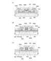
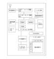
図1(A)乃至(E)に示すトランジスタ440aは、トップゲート構造を有するプレー
ナ型のトランジスタの例である。A
トランジスタ440aは、酸化物絶縁層436が設けられた絶縁表面を有する基板400
上に、チャネル形成領域409、低抵抗領域404a、404bを含む酸化物半導体層4
03、ソース電極層405a、ドレイン電極層405b、ゲート絶縁膜402、ゲート電
極層401を有する。トランジスタ440a上には、絶縁膜407が形成されている。The
03 , a
図1は、酸化物半導体層403上において、ソース電極層405a、及びドレイン電極層
405bとゲート電極層401とは重ならない構造であるが、図2(A)で示すトランジ
スタ440bのようにソース電極層405a、及びドレイン電極層405bとゲート電極
層401とが一部重なる構造であってもよい。1A and 1B show a structure in which the
酸化物半導体層403は、インジウム、ガリウム、亜鉛、及び酸素の4元素を少なくとも
含み、該4元素の組成比を原子百分率で表したとき、インジウムの割合が、ガリウムの割
合及び亜鉛の割合の2倍以上である酸化物半導体層(IGZO層ともいう)である。The
酸化物半導体層403は、インジウム:ガリウム:亜鉛の組成比が3:1:2の酸化物タ
ーゲットを用いたスパッタリング法によって作製することができる。The
酸化物半導体は非単結晶であり、アモルファスでも、多結晶でもよい。また、アモルファ
ス中に結晶性を有する部分を含む構造でも、非アモルファスでもよい。The oxide semiconductor is non-single-crystal, and may be amorphous or polycrystalline. In addition, it may be a structure including a portion having crystallinity in the amorphous, or may be non-amorphous.
アモルファス状態の酸化物半導体は、比較的容易に平坦な表面を得ることができるため、
これを用いてトランジスタを作製した際の界面散乱を低減でき、比較的容易に、比較的高
い移動度を得ることができる。A flat surface of an oxide semiconductor in an amorphous state can be obtained relatively easily.
Interfacial scattering can be reduced when a transistor is produced using this, and relatively high mobility can be obtained relatively easily.
また、結晶性を有する酸化物半導体では、よりバルク内欠陥を低減することができ、表面
の平坦性を高めればアモルファス状態の酸化物半導体以上の移動度を得ることができる。
表面の平坦性を高めるためには、平坦な表面上に酸化物半導体を形成することが好ましく
、具体的には、平均面粗さ(Ra)が1nm以下、好ましくは0.3nm以下、より好ま
しくは0.1nm以下の表面上に形成するとよい。In addition, in a crystalline oxide semiconductor, defects in the bulk can be further reduced, and if surface flatness is improved, mobility higher than that of an oxide semiconductor in an amorphous state can be obtained.
In order to improve the flatness of the surface, it is preferable to form the oxide semiconductor on a flat surface. Specifically, the average surface roughness (Ra) is 1 nm or less, preferably 0.3 nm or less, more preferably 0.3 nm or less. should be formed on the surface with a thickness of 0.1 nm or less.
なお、Raは、JIS B0601で定義されている算術平均粗さを面に対して適用でき
るよう三次元に拡張したものであり、「基準面から指定面までの偏差の絶対値を平均した
値」と表現でき、以下の式にて定義される。In addition, Ra is a three-dimensional extension of the arithmetic mean roughness defined in JIS B0601 so that it can be applied to a surface, and is "the average of the absolute values of the deviation from the reference surface to the designated surface". and is defined by the following formula.

なお、上記において、S0は、測定面(座標(x1,y1)(x1,y2)(x2,y1
)(x2,y2)で表される4点によって囲まれる長方形の領域)の面積を指し、Z0は
測定面の平均高さを指す。Raは原子間力顕微鏡(AFM:Atomic Force
Microscope)にて評価可能である。In the above, S0 is the measurement surface (coordinates (x1 , y1 ) (x1 , y2 ) (x2 , y1
) and Z0 refers tothe average heightof the measuring plane. Ra is an atomic force microscope (AFM: Atomic Force
Microscope) can be evaluated.
酸化物半導体層403として、結晶を含み、結晶性を有する酸化物半導体層(結晶性酸化
物半導体層)を用いることができる。結晶性酸化物半導体層における結晶状態は、結晶軸
の方向が無秩序な状態でも、一定の配向性を有する状態であってもよい。As the
例えば、結晶性酸化物半導体層として、表面に概略垂直なc軸を有している結晶を含む酸
化物半導体層を用いることができる。For example, as the crystalline oxide semiconductor layer, an oxide semiconductor layer containing crystals having a c-axis substantially perpendicular to the surface can be used.
表面に概略垂直なc軸を有している結晶を含む酸化物半導体層は、単結晶構造ではなく、
非晶質構造でもない構造であり、c軸配向を有した結晶(C Axis Aligned
Crystal;CAACともいう)を含む酸化物半導体(CAAC―OS)層である
。An oxide semiconductor layer containing crystals having a c-axis substantially perpendicular to the surface does not have a single crystal structure,
It is a structure that is not amorphous, and has a c-axis oriented crystal (C Axis Aligned
Crystal (also referred to as CAAC) is an oxide semiconductor (CAAC-OS) layer.
CAAC―OSとは、c軸配向し、かつab面、表面または界面に垂直な方向から見て三
角形状または六角形状の原子配列を有し、c軸に垂直な方向においては、金属原子が層状
または金属原子と酸素原子とが層状に配列しており、ab面(あるいは表面または界面)
においては、a軸またはb軸の向きが異なる(c軸を中心に回転した)結晶である。CA
ACを含む薄膜とは、c軸に対しては結晶化した薄膜であり、ab面に対しては必ずしも
配列していない。CAAC-OS is c-axis oriented and has a triangular or hexagonal atomic arrangement when viewed from a direction perpendicular to the ab plane, the surface, or the interface. Or metal atoms and oxygen atoms are arranged in layers, ab plane (or surface or interface)
is a crystal in which the orientation of the a-axis or the b-axis is different (rotated about the c-axis). CA
A thin film containing AC is a thin film that is crystallized with respect to the c-axis and is not necessarily aligned with respect to the ab-plane.
広義に、CAACとは、非単結晶であって、そのab面に垂直な方向から見て、三角形も
しくは六角形、または正三角形もしくは正六角形の原子配列を有し、かつc軸方向に垂直
な方向から見て金属原子が層状または金属原子と酸素原子が層状に配列した相を含む。In a broad sense, CAAC is a non-single crystal having a triangular or hexagonal, equilateral triangular or equilateral hexagonal atomic arrangement when viewed from the direction perpendicular to its ab plane, and It includes a phase in which metal atoms are arranged in layers or in which metal atoms and oxygen atoms are arranged in layers when viewed from the direction.
CAACを含む薄膜は単結晶ではないが、非晶質のみから形成されているものでもない。
また、CAACを含む薄膜は結晶化した部分(結晶部分)を含むが、1つの結晶部分と他
の結晶部分の境界を明確に判別できないこともある。A thin film containing CAAC is not a single crystal, but it is also not formed only of amorphous material.
In addition, although a thin film containing CAAC includes crystallized portions (crystal portions), the boundary between one crystal portion and another crystal portion may not be clearly discriminated.
CAACを構成する酸素の一部は窒素で置換されてもよい。また、CAACを含む薄膜を
構成する個々の結晶部分のc軸は一定の方向(例えば、CAACが形成される基板面やC
AACの表面や膜面、界面等に垂直な方向)に揃っていてもよい。あるいは、CAACを
含む薄膜を構成する個々の結晶部分のab面の法線は一定の方向(例えば、基板面、表面
、膜面、界面等に垂直な方向)を向いていてもよい。Part of the oxygen constituting CAAC may be replaced with nitrogen. In addition, the c-axes of the individual crystal parts constituting the CAAC-containing thin film are oriented in a fixed direction (for example, the substrate surface on which the CAAC is formed or the C-axis).
It may be aligned in a direction perpendicular to the surface, film surface, interface, etc. of AAC). Alternatively, the normals of the ab planes of the individual crystal portions forming the CAAC-containing thin film may be oriented in a certain direction (for example, a direction perpendicular to the substrate surface, surface, film surface, interface, etc.).
該結晶性酸化物半導体層とすることで、可視光や紫外光の照射によるトランジスタの電気
的特性変化をより抑制し、信頼性の高い半導体装置とすることができる。With the crystalline oxide semiconductor layer, change in electrical characteristics of the transistor due to irradiation with visible light or ultraviolet light can be suppressed, and the semiconductor device can have high reliability.
c軸配向を有した結晶性酸化物半導体層を得る方法としては、3つ挙げられる。1つ目は
、成膜温度を200℃以上500℃以下として酸化物半導体層の成膜を行い、表面に概略
垂直にc軸配向させる方法である。2つ目は、膜厚を薄く成膜した後、200℃以上70
0℃以下の加熱処理を行い、表面に概略垂直にc軸配向させる方法である。3つ目は、一
層目の膜厚を薄く成膜した後、200℃以上700℃以下の加熱処理を行い、2層目の成
膜を行い、表面に概略垂直にc軸配向させる方法である。There are three methods for obtaining a crystalline oxide semiconductor layer with c-axis alignment. The first method is to form an oxide semiconductor layer at a film formation temperature of 200° C. or higher and 500° C. or lower, and align the c-axis substantially perpendicular to the surface. Second, after forming a thin film,
In this method, a heat treatment is performed at 0° C. or lower to align the c-axis substantially perpendicular to the surface. The third method is to form a thin first layer and then heat-treat it at 200° C. or more and 700° C. or less to form a second layer and align the c-axis substantially perpendicular to the surface. .
酸化物半導体層403の膜厚は、1nm以上30nm以下(好ましくは5nm以上10n
m以下)とし、スパッタリング法、MBE(Molecular Beam Epita
xy)法、CVD法、パルスレーザ堆積法、ALD(Atomic Layer Dep
osition)法等を適宜用いることができる。また、酸化物半導体層403は、スパ
ッタリングターゲット表面に対し、概略垂直に複数の基板表面がセットされた状態で成膜
を行うスパッタ装置を用いて成膜してもよい。The film thickness of the
m or less), sputtering method, MBE (Molecular Beam Epita
xy) method, CVD method, pulsed laser deposition method, ALD (Atomic Layer Dep
position) method or the like can be used as appropriate. Alternatively, the
CAAC-OS膜は、例えば、多結晶である酸化物半導体スパッタリング用ターゲットを
用い、スパッタリング法によって成膜する。当該スパッタリング用ターゲットにイオンが
衝突すると、スパッタリング用ターゲットに含まれる結晶領域がa-b面から劈開し、a
-b面に平行な面を有する平板状またはペレット状のスパッタリング粒子として剥離する
ことがある。この場合、当該平板状のスパッタリング粒子が、結晶状態を維持したまま基
板に到達することで、CAAC-OS膜を成膜することができる。The CAAC-OS film is formed, for example, by a sputtering method using a polycrystalline oxide semiconductor sputtering target. When ions collide with the sputtering target, the crystal region included in the sputtering target is cleaved from the ab plane, and a
There are cases where the sputtered particles are exfoliated as plate-like or pellet-like sputtered particles having a plane parallel to the -b plane. In this case, the plate-like sputtered particles reach the substrate while maintaining their crystalline state, so that a CAAC-OS film can be formed.
また、CAAC-OS膜を成膜するために、以下の条件を適用することが好ましい。Further, it is preferable to apply the following conditions to form the CAAC-OS film.
成膜時の不純物混入を低減することで、不純物によって結晶状態が崩れることを抑制でき
る。例えば、成膜室内に存在する不純物濃度(水素、水、二酸化炭素および窒素など)を
低減すればよい。また、成膜ガス中の不純物濃度を低減すればよい。具体的には、露点が
-80℃以下、好ましくは-100℃以下である成膜ガスを用いる。By reducing the contamination of impurities during film formation, it is possible to suppress the deterioration of the crystal state due to the impurities. For example, the concentration of impurities (hydrogen, water, carbon dioxide, nitrogen, etc.) present in the film formation chamber may be reduced. Also, the impurity concentration in the deposition gas may be reduced. Specifically, a deposition gas having a dew point of −80° C. or lower, preferably −100° C. or lower is used.
また、成膜時の基板加熱温度を高めることで、基板到達後にスパッタリング粒子のマイグ
レーションが起こる。具体的には、基板加熱温度を100℃以上740℃以下、好ましく
は200℃以上500℃以下として成膜する。成膜時の基板加熱温度を高めることで、平
板状のスパッタリング粒子が基板に到達した場合、基板上でマイグレーションが起こり、
スパッタリング粒子の平らな面が基板に付着する。In addition, by increasing the substrate heating temperature during film formation, migration of sputtered particles occurs after reaching the substrate. Specifically, the film is formed at a substrate heating temperature of 100° C. or higher and 740° C. or lower, preferably 200° C. or higher and 500° C. or lower. By raising the substrate heating temperature during film formation, when flat plate-shaped sputtered particles reach the substrate, migration occurs on the substrate.
The flat sides of the sputtered particles adhere to the substrate.
また、成膜ガス中の酸素割合を高め、電力を最適化することで成膜時のプラズマダメージ
を軽減すると好ましい。成膜ガス中の酸素割合は、30体積%以上、好ましくは100体
積%とする。Further, it is preferable to reduce plasma damage during film formation by increasing the proportion of oxygen in the film forming gas and optimizing the power. The oxygen ratio in the film-forming gas is 30% by volume or more, preferably 100% by volume.
スパッタリング用ターゲットの一例として、In-Ga-Zn-O化合物ターゲットにつ
いて以下に示す。As an example of the sputtering target, an In--Ga--Zn--O compound target is shown below.
InOX粉末、GaOY粉末およびZnOZ粉末を所定のmol数比で混合し、加圧処理
後、1000℃以上1500℃以下の温度で加熱処理をすることで多結晶であるIn-G
a-Zn-O化合物ターゲットとする。なお、X、YおよびZは任意の正数である。ここ
で、所定のmol数比は、例えば、InOX粉末、GaOY粉末およびZnOZ粉末が、
2:2:1、8:4:3、3:1:1、1:1:1、4:2:3または3:1:2のmo
l数比である。なお、粉末の種類、およびその混合する比率は、作製するスパッタリング
用ターゲットによって適宜変更すればよい。InO2 X powder, GaO2 Y powder, and
An a-Zn-O compound target is used. Note that X, Y and Z are arbitrary positive numbers. Here, the predetermined molar ratio is such that, for example, InOX powder, GaOY powder, and ZnOZ powder are
2:2:1, 8:4:3, 3:1:1, 1:1:1, 4:2:3 or 3:1:2 mo
l number ratio. The types of powders and the mixing ratio thereof may be appropriately changed depending on the sputtering target to be produced.
図1(A)乃至(E)にトランジスタ440aを用いて、作製方法の一例を示す。1A to 1E illustrate an example of a manufacturing method using a
まず、絶縁表面を有する基板400上に酸化物絶縁層436を形成する。First, the
絶縁表面を有する基板400に使用することができる基板に大きな制限はないが、少なく
とも、後の熱処理に耐えうる程度の耐熱性を有していることが必要となる。例えば、バリ
ウムホウケイ酸ガラスやアルミノホウケイ酸ガラスなどのガラス基板、セラミック基板、
石英基板、サファイア基板などを用いることができる。また、シリコンや炭化シリコンな
どの単結晶半導体基板、多結晶半導体基板、シリコンゲルマニウムなどの化合物半導体基
板、SOI基板などを適用することもでき、これらの基板上に半導体素子が設けられたも
のを、基板400として用いてもよい。There is no particular limitation on the substrate that can be used as the
A quartz substrate, a sapphire substrate, or the like can be used. Further, a single crystal semiconductor substrate such as silicon or silicon carbide, a polycrystalline semiconductor substrate, a compound semiconductor substrate such as silicon germanium, an SOI substrate, or the like can also be applied. It may be used as the
また、基板400として、可撓性基板を用いて半導体装置を作製してもよい。可撓性を有
する半導体装置を作製するには、可撓性基板上に酸化物半導体層403を含むトランジス
タ440aを直接作製してもよいし、他の作製基板に酸化物半導体層403を含むトラン
ジスタ440aを作製し、その後可撓性基板に剥離、転置してもよい。なお、作製基板か
ら可撓性基板に剥離、転置するために、作製基板と酸化物半導体膜を含むトランジスタ4
40aとの間に剥離層を設けるとよい。Alternatively, a semiconductor device may be manufactured using a flexible substrate as the
It is preferable to provide a peeling layer between 40a.
酸化物絶縁層436としては、プラズマCVD法又はスパッタリング法等により、酸化シ
リコン、酸化窒化シリコン、酸化アルミニウム、酸化窒化アルミニウム、酸化ハフニウム
、酸化ガリウム、又はこれらの混合材料を用いて形成することができる。The
酸化物絶縁層436は、単層でも積層でもよい。例えば、基板400上に酸化シリコン膜
、In-Hf-Zn系酸化物膜、酸化物半導体層403を順に積層してもよいし、基板4
00上に酸化シリコン膜、In:Zr:Zn=1:1:1の原子数比のIn-Zr-Zn
系酸化物膜、酸化物半導体層403を順に積層してもよいし、基板400上に酸化シリコ
ン膜、In:Gd:Zn=1:1:1の原子数比のIn-Gd-Zn系酸化物膜、酸化物
半導体層403を順に積層してもよい。The
Silicon oxide film on 00, In--Zr--Zn with an atomic ratio of In:Zr:Zn=1:1:1
An oxide-based oxide film and an
本実施の形態では酸化物絶縁層436としてスパッタリング法を用いて形成する酸化シリ
コン膜を用いる。In this embodiment, a silicon oxide film formed by a sputtering method is used as the
また、酸化物絶縁層436と基板400との間に窒化物絶縁膜を設けてもよい。
窒化物絶縁膜は、プラズマCVD法又はスパッタリング法等により、窒化シリコン、窒化
酸化シリコン、窒化アルミニウム、窒化酸化アルミニウム、又はこれらの混合材料を用い
て形成することができる。Further, a nitride insulating film may be provided between the
The nitride insulating film can be formed using silicon nitride, silicon nitride oxide, aluminum nitride, aluminum nitride oxide, or a mixture thereof by a plasma CVD method, a sputtering method, or the like.
次に、酸化物絶縁層436上に酸化物半導体層403を形成する。Next, the
酸化物絶縁層436は、酸化物半導体層403と接するため、膜中(バルク中)に少なく
とも化学量論的組成比を超える量の酸素が存在することが好ましい。例えば、酸化物絶縁
層436として、酸化シリコン膜を用いる場合には、SiO2+α(ただし、α>0)と
する。このような酸化物絶縁層436を用いることで、酸化物半導体層403に酸素を供
給することができ、特性を良好にすることができる。酸化物半導体層403へ酸素を供給
することにより、膜中の酸素欠損を補填することができる。Since the
例えば、酸素の供給源となる酸素を多く(過剰に)含む酸化物絶縁層436を酸化物半導
体層403と接して設けることによって、該酸化物絶縁層436から酸化物半導体層40
3へ酸素を供給することができる。酸化物半導体層403及び酸化物絶縁層436を少な
くとも一部が接した状態で加熱処理を行うことによって酸化物半導体層403への酸素の
供給を行ってもよい。For example, the
3 can be supplied with oxygen. Oxygen may be supplied to the
酸化物半導体層403の形成工程において、酸化物半導体層403に水素、又は水がなる
べく含まれないようにするために、酸化物半導体層403の成膜の前処理として、スパッ
タリング装置の予備加熱室で酸化物絶縁層436が形成された基板を予備加熱し、基板及
び酸化物絶縁層436に吸着した水素、水分などの不純物を脱離し排気することが好まし
い。なお、予備加熱室に設ける排気手段はクライオポンプが好ましい。In order to prevent the
酸化物絶縁層436において酸化物半導体層403が接して形成される領域に、平坦化処
理を行ってもよい。平坦化処理としては、特に限定されないが、研磨処理(例えば、化学
的機械研磨(Chemical Mechanical Polishing:CMP)
法)、ドライエッチング処理、プラズマ処理を用いることができる。A region of the
method), dry etching treatment, and plasma treatment can be used.
プラズマ処理としては、例えば、アルゴンガスを導入してプラズマを発生させる逆スパッ
タリングを行うことができる。逆スパッタリングとは、アルゴン雰囲気下で基板側にRF
電源を用いて電圧を印加して基板近傍にプラズマを形成して表面を改質する方法である。
なお、アルゴン雰囲気に代えて窒素、ヘリウム、酸素などを用いてもよい。逆スパッタリ
ングを行うと、酸化物絶縁層436の表面に付着している粉状物質(パーティクル、ごみ
ともいう)を除去することができる。As the plasma treatment, for example, reverse sputtering in which argon gas is introduced to generate plasma can be performed. Reverse sputtering is RF sputtering on the substrate side in an argon atmosphere.
In this method, a voltage is applied using a power supply to form plasma in the vicinity of the substrate to modify the surface.
Note that nitrogen, helium, oxygen, or the like may be used instead of the argon atmosphere. By performing reverse sputtering, powdery substances (also referred to as particles or dust) attached to the surface of the
平坦化処理として、研磨処理、ドライエッチング処理、プラズマ処理は複数回行ってもよ
く、それらを組み合わせて行ってもよい。また、組み合わせて行う場合、工程順も特に限
定されず、酸化物絶縁層436表面の凹凸状態に合わせて適宜設定すればよい。As planarization treatment, polishing treatment, dry etching treatment, and plasma treatment may be performed a plurality of times or may be performed in combination. In the case of combining them, the order of steps is not particularly limited and may be set as appropriate according to the unevenness of the surface of the
なお、酸化物半導体層403は、成膜時に酸素が多く含まれるような条件(例えば、酸素
100%の雰囲気下でスパッタリング法により成膜を行うなど)で成膜して、酸素を多く
含む(好ましくは酸化物半導体が結晶状態における化学量論的組成比に対し、酸素の含有
量が過剰な領域が含まれている)膜とすることが好ましい。Note that the
なお、本実施の形態において、酸化物半導体層403を、スパッタリング法で作製するた
めのターゲットとしては、組成比として、In:Ga:Zn=3:1:2[原子百分率]
の酸化物ターゲットを用い、In-Ga-Zn系酸化物膜(IGZO膜)を成膜する。Note that in this embodiment, the target for manufacturing the
An In--Ga--Zn-based oxide film (IGZO film) is formed using an oxide target of .
また、金属酸化物ターゲットの相対密度(充填率)は90%以上100%以下、好ましく
は95%以上99.9%以下である。相対密度の高い金属酸化物ターゲットを用いること
により、成膜した酸化物半導体膜は緻密な膜とすることができる。Also, the relative density (filling rate) of the metal oxide target is 90% or more and 100% or less, preferably 95% or more and 99.9% or less. By using a metal oxide target with a high relative density, a dense oxide semiconductor film can be formed.
酸化物半導体層403を、成膜する際に用いるスパッタリングガスは水素、水、水酸基又
は水素化物などの不純物が除去された高純度ガスを用いることが好ましい。A high-purity gas from which impurities such as hydrogen, water, a hydroxyl group, or a hydride are removed is preferably used as a sputtering gas for forming the
減圧状態に保持された成膜室内に基板を保持する。そして、成膜室内の残留水分を除去し
つつ水素及び水分が除去されたスパッタガスを導入し、上記ターゲットを用いて基板40
0上に酸化物半導体層403を成膜する。成膜室内の残留水分を除去するためには、吸着
型の真空ポンプ、例えば、クライオポンプ、イオンポンプ、チタンサブリメーションポン
プを用いることが好ましい。また、排気手段としては、ターボ分子ポンプにコールドトラ
ップを加えたものであってもよい。クライオポンプを用いて排気した成膜室は、例えば、
水素原子、水(H2O)など水素原子を含む化合物(より好ましくは炭素原子を含む化合
物も)等が排気されるため、当該成膜室で成膜した酸化物半導体層403に含まれる不純
物の濃度を低減できる。A substrate is held in a deposition chamber kept in a reduced pressure state. Then, a sputtering gas from which hydrogen and moisture are removed is introduced while removing residual moisture in the deposition chamber, and the
0, an
Since a compound containing a hydrogen atom (preferably a compound containing a carbon atom) such as a hydrogen atom or water (H2 O) is exhausted, impurities contained in the
また、酸化物絶縁層436と酸化物半導体層403とを大気に解放せずに連続的に形成す
ることが好ましい。酸化物絶縁層436と酸化物半導体層403とを大気に曝露せずに連
続して形成すると、酸化物絶縁層436表面に水素や水分などの不純物が吸着することを
防止することができる。Further, the
酸化物半導体層403は、膜状の酸化物半導体膜をフォトリソグラフィ工程により島状の
酸化物半導体層に加工して形成することができる。The
また、島状の酸化物半導体層403を形成するためのレジストマスクをインクジェット法
で形成してもよい。レジストマスクをインクジェット法で形成するとフォトマスクを使用
しないため、製造コストを低減できる。Alternatively, a resist mask for forming the island-shaped
なお、酸化物半導体膜のエッチングは、ドライエッチングでもウェットエッチングでもよ
く、両方を用いてもよい。例えば、酸化物半導体膜のウェットエッチングに用いるエッチ
ング液としては、燐酸と酢酸と硝酸を混ぜた溶液などを用いることができる。また、IT
O07N(関東化学社製)を用いてもよい。Note that the etching of the oxide semiconductor film may be dry etching, wet etching, or both. For example, as an etchant used for wet etching of the oxide semiconductor film, a mixed solution of phosphoric acid, acetic acid, and nitric acid, or the like can be used. Also, IT
O07N (manufactured by Kanto Kagaku Co., Ltd.) may also be used.
また、酸化物半導体層403に、過剰な水素(水や水酸基を含む)を除去(脱水化または
脱水素化)するための加熱処理を行ってもよい。加熱処理の温度は、300℃以上700
℃以下、または基板の歪み点未満とする。加熱処理は減圧下又は窒素雰囲気下などで行う
ことができる。例えば、加熱処理装置の一つである電気炉に基板を導入し、酸化物半導体
層403に対して窒素雰囲気下450℃において1時間の加熱処理を行う。Further, the
°C or below the strain point of the substrate. The heat treatment can be performed under reduced pressure, a nitrogen atmosphere, or the like. For example, the substrate is introduced into an electric furnace which is one of heat treatment apparatuses, and heat treatment is performed on the
なお、加熱処理装置は電気炉に限られず、抵抗発熱体などの発熱体からの熱伝導または熱
輻射によって、被処理物を加熱する装置を用いてもよい。例えば、GRTA(Gas R
apid Thermal Anneal)装置、LRTA(Lamp Rapid T
hermal Anneal)装置等のRTA(Rapid Thermal Anne
al)装置を用いることができる。LRTA装置は、ハロゲンランプ、メタルハライドラ
ンプ、キセノンアークランプ、カーボンアークランプ、高圧ナトリウムランプ、高圧水銀
ランプなどのランプから発する光(電磁波)の輻射により、被処理物を加熱する装置であ
る。GRTA装置は、高温のガスを用いて加熱処理を行う装置である。高温のガスには、
アルゴンなどの希ガス、または窒素のような、加熱処理によって被処理物と反応しない不
活性気体が用いられる。Note that the heat treatment apparatus is not limited to an electric furnace, and an apparatus that heats an object to be treated by heat conduction or heat radiation from a heating element such as a resistance heating element may be used. For example, GRTA (Gas R
apid Thermal Anneal) device, LRTA (Lamp Rapid T
RTA (rapid thermal anneal) such as a thermal anneal) device
al) the device can be used; An LRTA apparatus is an apparatus that heats an object by radiation of light (electromagnetic waves) emitted from lamps such as halogen lamps, metal halide lamps, xenon arc lamps, carbon arc lamps, high pressure sodium lamps, and high pressure mercury lamps. The GRTA apparatus is an apparatus that performs heat treatment using high-temperature gas. For hot gases,
A rare gas such as argon or an inert gas such as nitrogen that does not react with the object to be processed by heat treatment is used.
例えば、加熱処理として、650℃~700℃の高温に加熱した不活性ガス中に基板を入
れ、数分間加熱した後、基板を不活性ガス中から出すGRTAを行ってもよい。For example, as the heat treatment, GRTA may be performed in which the substrate is placed in an inert gas heated to a high temperature of 650° C. to 700° C., heated for several minutes, and then taken out of the inert gas.
なお、加熱処理においては、窒素、またはヘリウム、ネオン、アルゴン等の希ガスに、水
、水素などが含まれないことが好ましい。または、熱処理装置に導入する窒素、またはヘ
リウム、ネオン、アルゴン等の希ガスの純度を、6N(99.9999%)以上好ましく
は7N(99.99999%)以上(即ち不純物濃度を1ppm以下、好ましくは0.1
ppm以下)とすることが好ましい。Note that in the heat treatment, nitrogen or a rare gas such as helium, neon, or argon preferably does not contain water, hydrogen, or the like. Alternatively, the purity of nitrogen or rare gases such as helium, neon, argon, etc. introduced into the heat treatment apparatus is 6N (99.9999%) or more, preferably 7N (99.99999%) or more (that is, the impurity concentration is 1 ppm or less, preferably is 0.1
ppm or less).
また、加熱処理で酸化物半導体層403を加熱した後、同じ炉に高純度の酸素ガス、高純
度の一酸化二窒素ガス、又は超乾燥エア(CRDS(キャビティリングダウンレーザー分
光法)方式の露点計を用いて測定した場合の水分量が20ppm(露点換算で-55℃)
以下、好ましくは1ppm以下、より好ましくは10ppb以下の空気)を導入してもよ
い。酸素ガスまたは一酸化二窒素ガスに、水、水素などが含まれないことが好ましい。ま
たは、熱処理装置に導入する酸素ガスまたは一酸化二窒素ガスの純度を、6N以上好まし
くは7N以上(即ち、酸素ガスまたは一酸化二窒素ガス中の不純物濃度を1ppm以下、
好ましくは0.1ppm以下)とすることが好ましい。酸素ガス又は一酸化二窒素ガスの
作用により、脱水化または脱水素化処理による不純物の排除工程によって同時に減少して
しまった酸化物半導体を構成する主成分材料である酸素を供給することによって、酸化物
半導体層403を高純度化及び電気的にI型(真性)化することができる。Further, after the
(preferably 1 ppm or less, more preferably 10 ppb or less air) may be introduced. Oxygen gas or nitrous oxide gas preferably does not contain water, hydrogen, or the like. Alternatively, the purity of the oxygen gas or dinitrogen monoxide gas introduced into the heat treatment apparatus is 6N or more, preferably 7N or more (that is, the impurity concentration in the oxygen gas or dinitrogen monoxide gas is 1 ppm or less,
preferably 0.1 ppm or less). Oxidation is achieved by supplying oxygen, which is the main component material constituting the oxide semiconductor, which has been simultaneously reduced by the process of removing impurities by dehydration or dehydrogenation by the action of oxygen gas or dinitrogen monoxide gas. The
なお、脱水化又は脱水素化のための加熱処理は、酸化物半導体層403加工前の膜状の酸
化物半導体膜の形成後、絶縁膜407の形成前であれば、トランジスタ440aの作製工
程においてどのタイミングで行ってもよい。例えば、膜状の酸化物半導体膜の形成後、又
は島状の酸化物半導体層403形成後に行うことができる。Note that the heat treatment for dehydration or dehydrogenation is performed in the manufacturing process of the
また、脱水化又は脱水素化のための加熱処理は、複数回行ってもよく、他の加熱処理と兼
ねてもよい。Further, the heat treatment for dehydration or dehydrogenation may be performed multiple times or may be combined with other heat treatments.
脱水化又は脱水素化のための加熱処理を、酸化物半導体層403として島状に加工される
前、膜状の酸化物半導体膜が酸化物絶縁層436を覆った状態で行うと、酸化物絶縁層4
36に含まれる酸素が加熱処理によって放出されるのを防止することができるため好まし
い。When heat treatment for dehydration or dehydrogenation is performed in a state in which the
It is preferable because the oxygen contained in 36 can be prevented from being released by the heat treatment.
また、脱水化又は脱水素化処理を行った酸化物半導体層に、酸素(少なくとも、酸素ラジ
カル、酸素原子、酸素イオン、のいずれかを含む)を導入して膜中に酸素を供給してもよ
い。Alternatively, oxygen (containing at least one of oxygen radicals, oxygen atoms, and oxygen ions) may be introduced into the oxide semiconductor layer that has been subjected to dehydration or dehydrogenation treatment to supply oxygen into the film. good.
脱水化又は脱水素化処理を行った酸化物半導体層403に、酸素を導入して膜中に酸素を
供給することによって、酸化物半導体層403を高純度化、及び電気的にI型(真性)化
することができる。高純度化し、電気的にI型(真性)化した酸化物半導体層403を有
するトランジスタは、電気特性変動が抑制されており、電気的に安定である。By introducing oxygen into the
酸素の導入方法としては、イオン注入法、イオンドーピング法、プラズマイマージョンイ
オンインプランテーション法、プラズマ処理などを用いることができる。As a method for introducing oxygen, an ion implantation method, an ion doping method, a plasma immersion ion implantation method, plasma treatment, or the like can be used.
酸素の導入工程は、酸化物半導体層403に酸素導入する場合、酸化物半導体層403に
直接導入してもよいし、ゲート絶縁膜402や絶縁膜407などの他の膜を通過して酸化
物半導体層403へ導入してもよい。酸素を他の膜を通過して導入する場合は、イオン注
入法、イオンドーピング法、プラズマイマージョンイオンインプランテーション法などを
用いればよいが、酸素を露出された酸化物半導体層403へ直接導入する場合は、プラズ
マ処理なども用いることができる。In the step of introducing oxygen, when oxygen is introduced into the
酸化物半導体層403への酸素の導入は、脱水化又は脱水素化処理を行った後であればよ
く、特に限定されない。また、上記脱水化又は脱水素化処理を行った酸化物半導体層40
3への酸素の導入は複数回行ってもよい。Introduction of oxygen into the
Introduction of oxygen to 3 may be performed multiple times.
次いで、酸化物半導体層403上に、ソース電極層及びドレイン電極層(これと同じ層で
形成される配線を含む)となる導電膜を形成する。該導電膜は後の加熱処理に耐えられる
材料を用いる。ソース電極層、及びドレイン電極層に用いる導電膜としては、例えば、A
l、Cr、Cu、Ta、Ti、Mo、Wから選ばれた元素を含む金属膜、または上述した
元素を成分とする金属窒化物膜(窒化チタン膜、窒化モリブデン膜、窒化タングステン膜
)等を用いることができる。また、Al、Cuなどの金属膜の下側又は上側の一方または
双方にTi、Mo、Wなどの高融点金属膜またはそれらの金属窒化物膜(窒化チタン膜、
窒化モリブデン膜、窒化タングステン膜)を積層させた構成としても良い。また、ソース
電極層、及びドレイン電極層に用いる導電膜としては、導電性の金属酸化物で形成しても
良い。導電性の金属酸化物としては酸化インジウム(In2O3)、酸化スズ(SnO2
)、酸化亜鉛(ZnO)、酸化インジウム酸化スズ(In2O3―SnO2)、酸化イン
ジウム酸化亜鉛(In2O3―ZnO)またはこれらの金属酸化物材料に酸化シリコンを
含ませたものを用いることができる。Next, a conductive film to be a source electrode layer and a drain electrode layer (including wirings formed using the same layers) is formed over the
A metal film containing an element selected from l, Cr, Cu, Ta, Ti, Mo, and W, or a metal nitride film (titanium nitride film, molybdenum nitride film, tungsten nitride film) containing the above elements as components, or the like. can be used. In addition, a high melting point metal film such as Ti, Mo, W or a metal nitride film thereof (titanium nitride film,
A molybdenum nitride film, a tungsten nitride film) may be laminated. Alternatively, the conductive film used for the source electrode layer and the drain electrode layer may be formed using a conductive metal oxide. Indium oxide (In2 O3 ), tin oxide (SnO2
), zinc oxide (ZnO), indium tin oxide (In2 O3 —SnO2 ), indium zinc oxide (In2 O3 —ZnO), or those metal oxide materials containing silicon oxide. can be used.
フォトリソグラフィ工程により導電膜上にレジストマスクを形成し、選択的にエッチング
を行ってソース電極層405a、ドレイン電極層405bを形成した後、レジストマスク
を除去する。A resist mask is formed over the conductive film by a photolithography step, etching is selectively performed to form the
次いで、酸化物半導体層403、ソース電極層405a、及びドレイン電極層405bを
覆うゲート絶縁膜402を形成する(図1(C)参照)。Next, a
なお、ゲート絶縁膜402の被覆性を向上させるために、酸化物半導体層403、ソース
電極層405a、及びドレイン電極層405b表面にも上記平坦化処理を行ってもよい。
特にゲート絶縁膜402として膜厚の薄い絶縁膜を用いる場合、酸化物半導体層403、
ソース電極層405a、及びドレイン電極層405b表面の平坦性が良好であることが好
ましい。Note that in order to improve coverage with the
In particular, when a thin insulating film is used as the
The surfaces of the
ゲート絶縁膜402の膜厚は、1nm以上20nm以下とし、スパッタリング法、MBE
法、CVD法、パルスレーザ堆積法、ALD法等を適宜用いることができる。また、ゲー
ト絶縁膜402は、スパッタリングターゲット表面に対し、概略垂直に複数の基板表面が
セットされた状態で成膜を行うスパッタ装置を用いて成膜してもよい。The film thickness of the
method, CVD method, pulse laser deposition method, ALD method, or the like can be used as appropriate. Alternatively, the
ゲート絶縁膜402の材料としては、酸化シリコン膜、酸化ガリウム膜、酸化アルミニウ
ム膜、窒化シリコン膜、酸化窒化シリコン膜、酸化窒化アルミニウム膜、または窒化酸化
シリコン膜を用いて形成することができる。ゲート絶縁膜402は、酸化物半導体層40
3と接する部分において酸素を含むことが好ましい。特に、ゲート絶縁膜402は、膜中
(バルク中)に少なくとも化学量論的組成比を超える量の酸素が存在することが好ましく
、例えば、ゲート絶縁膜402として、酸化シリコン膜を用いる場合には、SiO2+α
(ただし、α>0)とする。本実施の形態では、ゲート絶縁膜402として、SiO2+
α(ただし、α>0)である酸化シリコン膜を用いる。この酸化シリコン膜をゲート絶縁
膜402として用いることで、酸化物半導体層403に酸素を供給することができ、特性
を良好にすることができる。さらに、ゲート絶縁膜402は、作製するトランジスタのサ
イズやゲート絶縁膜402の段差被覆性を考慮して形成することが好ましい。As a material for the
It is preferable that the portion in contact with 3 contain oxygen. In particular, the
(where α>0). In this embodiment mode, SiO2+ is used as the
A silicon oxide film satisfyingα (where α>0) is used. By using this silicon oxide film as the
また、ゲート絶縁膜402の材料として酸化ハフニウム、酸化イットリウム、ハフニウム
シリケート(HfSixOy(x>0、y>0))、窒素が添加されたハフニウムシリケ
ート(HfSiOxNy(x>0、y>0))、ハフニウムアルミネート(HfAlxO
y(x>0、y>0))、酸化ランタンなどのhigh-k材料を用いることでゲートリ
ーク電流を低減できる。さらに、ゲート絶縁膜402は、単層構造としても良いし、積層
構造としても良い。Hafnium oxide, yttrium oxide, hafnium silicate (HfSix Oy (x>0, y>0)), and nitrogen-added hafnium silicate (HfSiOx Ny (x>0, y>0)), hafnium aluminate (HfAlx O
y (x>0, y>0)) and high-k materials such as lanthanum oxide can reduce the gate leakage current. Furthermore, the
そして、ゲート電極層401をプラズマCVD法又はスパッタリング法等により、ゲート
絶縁膜402上に形成する(図1(B)参照)。ゲート電極層401の材料は、モリブデ
ン、チタン、タンタル、タングステン、アルミニウム、銅、クロム、ネオジム、スカンジ
ウム等の金属材料またはこれらを主成分とする合金材料を用いて形成することができる。
また、ゲート電極層401としてリン等の不純物元素をドーピングした多結晶シリコン膜
に代表される半導体膜、ニッケルシリサイドなどのシリサイド膜を用いてもよい。ゲート
電極層401は、単層構造としてもよいし、積層構造としてもよい。Then, a
Alternatively, a semiconductor film typified by a polycrystalline silicon film doped with an impurity element such as phosphorus, or a silicide film such as nickel silicide may be used as the
また、ゲート電極層401の材料は、インジウム錫酸化物、酸化タングステンを含むイン
ジウム酸化物、酸化タングステンを含むインジウム亜鉛酸化物、酸化チタンを含むインジ
ウム酸化物、酸化チタンを含むインジウム錫酸化物、インジウム亜鉛酸化物、酸化ケイ素
を添加したインジウム錫酸化物などの導電性材料を適用することもできる。また、上記導
電性材料と、上記金属材料の積層構造とすることもできる。Materials for the
また、ゲート絶縁膜402と接するゲート電極層401の一層として、窒素を含む金属酸
化物、具体的には、窒素を含むIn-Ga-Zn-O膜や、窒素を含むIn-Sn-O膜
や、窒素を含むIn-Ga-O膜や、窒素を含むIn-Zn-O膜や、窒素を含むSn-
O膜や、窒素を含むIn-O膜や、金属窒化膜(InN、SnNなど)を用いることがで
きる。これらの膜は5eV(電子ボルト)、好ましくは5.5eV(電子ボルト)以上の
仕事関数を有し、ゲート電極層として用いた場合、トランジスタの電気特性のしきい値電
圧をプラスにすることができ、所謂ノーマリーオフのスイッチング素子を実現できる。Further, as one layer of the
An O film, an In—O film containing nitrogen, or a metal nitride film (InN, SnN, etc.) can be used. These films have a work function of 5 eV (electron volt), preferably 5.5 eV (electron volt) or more, and when used as a gate electrode layer, the threshold voltage of electrical characteristics of the transistor can be made positive. Thus, a so-called normally-off switching element can be realized.
次に、ゲート電極層401、ソース電極層405a、及びドレイン電極層405bをマス
クとして酸化物半導体層403にドーパント421を導入し、低抵抗領域404a、40
4bを形成する。Next, a
4b is formed.
ソース電極層405a、及びドレイン電極層405bの膜厚や、ドーパント421の導入
条件によっては、ソース電極層405a、及びドレイン電極層405b下の酸化物半導体
層403にもドーパント421が導入される場合と導入されない場合があり、また導入さ
れても濃度が低くソース電極層405a、又はドレイン電極層405b下以外の低抵抗領
域と比べて抵抗が高い領域となる場合もある。Depending on the film thicknesses of the
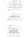
図2(B)で示すトランジスタ440cは、ソース電極層405a、ドレイン電極層40
5bとして膜厚の薄い、例えば10nmのタングステン膜を形成する。このようにソース
電極層405a、ドレイン電極層405bの膜厚が薄いと、低抵抗領域を形成するために
酸化物半導体層403へドーパントを導入する場合、ソース電極層405a、ドレイン電
極層405bを通過してソース電極層405a、ドレイン電極層405b下の酸化物半導
体層403にもドーパントを導入することができる。従って、トランジスタ440cはソ
ース電極層405a、ドレイン電極層405b下の酸化物半導体層403の領域も低抵抗
領域404a、404bが形成されている。A
As 5b, a thin tungsten film having a thickness of, for example, 10 nm is formed. When the thickness of the
ドーパント421は、酸化物半導体層403の導電率を変化させる不純物である。ドーパ
ント421としては、15族元素(代表的にはリン(P)、砒素(As)、およびアンチ
モン(Sb))、ホウ素(B)、アルミニウム(Al)、窒素(N)、アルゴン(Ar)
、ヘリウム(He)、ネオン(Ne)、インジウム(In)、フッ素(F)、塩素(Cl
)、チタン(Ti)、及び亜鉛(Zn)のいずれかから選択される一以上を用いることが
できる。A
, helium (He), neon (Ne), indium (In), fluorine (F), chlorine (Cl
), titanium (Ti), and zinc (Zn).
ドーパント421は、注入法により、他の膜(例えば絶縁膜407、ソース電極層405
a、及びドレイン電極層405b)を通過して、酸化物半導体層403に導入することも
できる。ドーパント421の導入方法としては、イオン注入法、イオンドーピング法、プ
ラズマイマージョンイオンインプランテーション法などを用いることができる。その際に
は、ドーパント421の単体のイオンあるいはフッ化物、塩化物のイオンを用いると好ま
しい。The
It can also be introduced into the
ドーパント421の導入工程は、加速電圧、ドーズ量などの注入条件、また通過させる膜
の膜厚を適宜設定して制御すればよい。本実施の形態では、ドーパント421としてホウ
素を用いて、イオン注入法でホウ素イオンの注入を行う。なお、ドーパント421のドー
ズ量は1×10¹³ions/cm2以上5×1016ions/cm2以下とすればよ
い。The step of introducing the
低抵抗領域におけるドーパント421の濃度は、5×10¹⁸/cm3以上1×1022
/cm3以下であることが好ましい。The concentration of the
/cm3 or less.
ドーパント421を導入する際に、基板400を加熱しながら行ってもよい。The
なお、酸化物半導体層403にドーパント421を導入する処理は、複数回行ってもよく
、ドーパントの種類も複数種用いてもよい。Note that the treatment for introducing the
また、ドーパント421の導入処理後、加熱処理を行ってもよい。加熱条件としては、温
度300℃以上700℃以下、好ましくは300℃以上450℃以下で1時間、酸素雰囲
気下で行うことが好ましい。また、窒素雰囲気下、減圧下、大気(超乾燥エア)下で加熱
処理を行ってもよい。Further, heat treatment may be performed after the introduction treatment of the
酸化物半導体層403を結晶性酸化物半導体膜とした場合、ドーパント421の導入によ
り、一部非晶質化する場合がある。この場合、ドーパント421の導入後に加熱処理を行
うことによって、酸化物半導体層403の結晶性を回復することができる。In the case where the
よって酸化物半導体層403において、チャネル形成領域409を挟んで低抵抗領域40
4a、404bが設けられた酸化物半導体層403が形成される。Therefore, in the
An
以上の工程で、本実施の形態のトランジスタ440aが作製される(図1(C)参照)。
インジウム、ガリウム、亜鉛、及び酸素の4元素を少なくとも含み、該4元素の組成比を
原子百分率で表したとき、インジウムの割合が、ガリウムの割合及び亜鉛の割合の2倍以
上であるIGZO膜を用いた酸化物半導体層403を用いることによって、トランジスタ
440aに高いオン特性(電界効果移動度)、低いオフ電流、高い信頼性を付与すること
が可能となる。Through the above steps, the
An IGZO film containing at least four elements of indium, gallium, zinc, and oxygen, wherein the proportion of indium is at least twice the proportion of gallium and zinc when the composition ratio of the four elements is expressed as an atomic percentage. By using the
次いで、酸化物半導体層403、ソース電極層405a、ドレイン電極層405b、ゲー
ト絶縁膜402、ゲート電極層401上に絶縁膜407を形成する(図1(D)参照)。Next, an insulating
絶縁膜407は、プラズマCVD法、スパッタリング法、又は蒸着法等により成膜するこ
とができる。絶縁膜407は、代表的には酸化シリコン膜、酸化窒化シリコン膜、酸化窒
化アルミニウム膜、又は酸化ガリウム膜などの無機絶縁膜などを用いることができる。The insulating
また、絶縁膜407として、酸化アルミニウム膜、酸化ハフニウム膜、酸化マグネシウム
膜、酸化ジルコニウム膜、酸化ランタン膜、酸化バリウム膜)、又は金属窒化物膜(例え
ば、窒化アルミニウム膜)も用いることができる。As the insulating
絶縁膜407は、単層でも積層でもよく、例えば酸化シリコン膜及び酸化アルミニウム膜
の積層を用いることができる。The insulating
絶縁膜407は、スパッタリング法など、絶縁膜407に水、水素等の不純物を混入させ
ない方法を適宜用いて形成することが好ましい。また、絶縁膜407において、酸化物半
導体層403に接する絶縁膜は、酸素を過剰に含む膜とすると、酸化物半導体層403へ
の酸素の供給源となるために好ましい。The insulating
本実施の形態では、絶縁膜407として膜厚100nmの酸化シリコン膜を、スパッタリ
ング法を用いて成膜する。酸化シリコン膜のスパッタリング法による成膜は、希ガス(代
表的にはアルゴン)雰囲気下、酸素雰囲気下、または希ガスと酸素の混合雰囲気下におい
て行うことができる。In this embodiment mode, a 100-nm-thick silicon oxide film is formed as the insulating
酸化物半導体膜の成膜時と同様に、絶縁膜407の成膜室内の残留水分を除去するために
は、吸着型の真空ポンプ(クライオポンプなど)を用いることが好ましい。クライオポン
プを用いて排気した成膜室で成膜した絶縁膜407に含まれる不純物の濃度を低減できる
。また、絶縁膜407の成膜室内の残留水分を除去するための排気手段としては、ターボ
分子ポンプにコールドトラップを加えたものであってもよい。In order to remove moisture remaining in the deposition chamber for the insulating
絶縁膜407を、成膜する際に用いるスパッタガスとしては、水素、水、水酸基又は水素
化物などの不純物が除去された高純度ガスを用いることが好ましい。As a sputtering gas for forming the insulating
酸化物半導体層403上に設けられる絶縁膜407として用いることのできる酸化アルミ
ニウム膜は、水素、水分などの不純物、及び酸素の両方に対して膜を通過させない遮断効
果(ブロック効果)が高い。An aluminum oxide film that can be used as the insulating
従って、酸化アルミニウム膜は、作製工程中及び作製後において、変動要因となる水素、
水分などの不純物の酸化物半導体層403への混入、及び酸化物半導体を構成する主成分
材料である酸素の酸化物半導体層403からの放出を防止する保護膜として機能する。Therefore, the aluminum oxide film contains hydrogen, which is a variable factor during and after the manufacturing process.
It functions as a protective film that prevents impurities such as moisture from entering the
また、トランジスタ起因の表面凹凸を低減するために平坦化絶縁膜を形成してもよい。平
坦化絶縁膜としては、ポリイミド、アクリル、ベンゾシクロブテン系樹脂、等の有機材料
を用いることができる。また上記有機材料の他に、低誘電率材料(low-k材料)等を
用いることができる。なお、これらの材料で形成される絶縁膜を複数積層させることで、
平坦化絶縁膜を形成してもよい。Further, a planarization insulating film may be formed in order to reduce surface unevenness caused by the transistor. Organic materials such as polyimide, acryl, and benzocyclobutene-based resins can be used as the planarization insulating film. In addition to the above organic materials, low dielectric constant materials (low-k materials) and the like can be used. By stacking a plurality of insulating films made of these materials,
A planarization insulating film may be formed.
また、ゲート絶縁膜402及び絶縁膜407にソース電極層405a、ドレイン電極層4
05bに達する開口を形成し、開口にソース電極層405a、ドレイン電極層405bと
電気的に接続する配線層465a、465bを形成する(図1(E)参照)。配線層46
5a、465bを用いて他のトランジスタと接続させ、様々な回路を構成することができ
る。In addition, the
An opening reaching 05b is formed, and
5a and 465b can be used to connect to other transistors to form various circuits.
また、図2(C)に示すトランジスタ440dのように、ソース電極層405a、ドレイ
ン電極層405bを設けずに、酸化物半導体層403に直接配線層465a、465bを
接するように設けてもよい。Alternatively,
配線層465a、配線層465bはゲート電極層401、ソース電極層405a、405
bと同様の材料及び方法を用いて形成することができる。例えば、配線層465a、配線
層465bとして窒化タンタル膜と銅膜との積層、又は窒化タンタル膜とタングステン膜
との積層などを用いることができる。The
It can be formed using the same material and method as b. For example, a stack of a tantalum nitride film and a copper film, a stack of a tantalum nitride film and a tungsten film, or the like can be used as the
高純度化され、酸素欠損が補填された酸化物半導体層403は、水素、水などの不純物が
十分に除去されており、酸化物半導体層403中の水素濃度は5×10¹⁹/cm3以下
、好ましくは5×10¹⁸/cm3以下である。なお、酸化物半導体層403中の水素濃
度は、二次イオン質量分析法(SIMS:Secondary Ion Mass Sp
ectrometry)で測定されるものである。Impurities such as hydrogen and water are sufficiently removed from the highly purified
electrometry).
本実施の形態を用いて作製した、高純度化し、酸素欠損を補填する酸素を過剰に含む酸化
物半導体層403を用いたトランジスタ440aは、オフ状態における電流値(オフ電流
値)を、チャネル幅1μm当たり室温にて100zA/μm(1zA(ゼプトアンペア)
は1×10-21A)以下、好ましくは50zA/μm以下レベルにまで低くすることが
できる。In the
can be lowered to a level of 1×10⁻²¹ A) or less, preferably 50 zA/μm or less.
以上のように、酸化物半導体をチャネル形成領域に用いたトランジスタの電気特性のしき
い値電圧をプラスにすることができ、所謂ノーマリーオフのスイッチング素子を実現する
トランジスタ構造およびその作製方法を提供することができる。As described above, a transistor structure in which the threshold voltage of electrical characteristics of a transistor using an oxide semiconductor for a channel formation region can be made positive and a so-called normally-off switching element is realized, and a manufacturing method thereof is provided. can do.
また、より高性能な半導体装置を実現するため、トランジスタのオン特性(例えば、オン
電流や電界効果移動度)を向上させて、半導体装置の高速応答、高速駆動を実現する構成
およびその作製方法を提供することができる。In addition, in order to realize a semiconductor device with higher performance, we will develop a structure and a manufacturing method for realizing high-speed response and high-speed driving of a semiconductor device by improving the on-characteristics (for example, on-current and field-effect mobility) of a transistor. can provide.
また、長期間の使用に際しても、しきい値電圧が変動しにくく、信頼性の高い半導体装置
を提供することができる。In addition, it is possible to provide a highly reliable semiconductor device in which the threshold voltage is less likely to fluctuate even when used for a long period of time.
(実施の形態2)
本実施の形態では、半導体装置及び半導体装置の作製方法の他の一形態を、図3及び図4
を用いて説明する。上記実施の形態と同一部分又は同様な機能を有する部分、及び工程は
、上記実施の形態と同様に行うことができ、繰り返しの説明は省略する。また同じ箇所の
詳細な説明は省略する。(Embodiment 2)
In this embodiment mode, another mode of a semiconductor device and a method for manufacturing a semiconductor device is described with reference to FIGS.
will be used to explain. Portions that are the same as or have similar functions to those in the above embodiment, and steps can be performed in the same manner as in the above embodiment, and repeated description will be omitted. Further, detailed description of the same parts will be omitted.
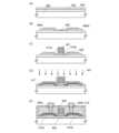
図3(A)乃至(C)に示すトランジスタ450は、トップゲート構造のトランジスタの
一例である。図3(A)は平面図であり、図3(A)中の一点鎖線X-Yで切断した断面
が図3(B)に相当し、図3(A)中の一点鎖線V-Wで切断した断面が図3(C)に相
当する。A
チャネル長方向の断面図である図3(B)に示すように、トランジスタ450は、酸化物
絶縁層436が設けられた絶縁表面を有する基板400上に、第1の酸化物半導体層であ
る酸化物半導体層408a、408b、チャネル形成領域409、低抵抗領域414a、
414bを含む第2の酸化物半導体層である酸化物半導体層403、ソース電極層405
a、ドレイン電極層405b、ゲート絶縁膜402、ゲート電極層401を有する。酸化
物半導体層408a、408bは、酸化物絶縁層436上に接して間隔を有して形成され
、酸化物半導体層403は酸化物半導体層408a、408b及び酸化物絶縁層436と
接して形成される。As illustrated in FIG. 3B which is a cross-sectional view in the channel length direction, the
The
a, a
図3(C)は、チャネル幅方向の断面図であり、酸化物半導体層403は端部に20度~
50度のテーパーを有している。端部が垂直であると酸素が抜けやすく酸素欠陥を生じや
すいが、端部にテーパーを有することで酸素欠陥を抑制し、トランジスタ450のリーク
電流(寄生チャネル)の発生を低減している。FIG. 3C is a cross-sectional view in the channel width direction.
It has a taper of 50 degrees. If the edge is vertical, oxygen easily escapes and oxygen defects are likely to occur.
膜厚3~5nmの酸化物半導体層403の下に酸化物半導体層408a、408bを設け
ることで、ソース電極層405a、405bとのコンタクト抵抗を低下させることができ
る。By providing the
低抵抗領域414a、414bはゲート電極層401をマスクとして酸化物半導体層40
3へドーパントを導入することで形成することができる。また、低抵抗領域は金属元素を
拡散させることによっても形成することができる。ドーパント及び金属元素の拡散を用い
て低抵抗領域を形成することで、より配線層とのコンタクト抵抗を低下させることができ
る。The low-
It can be formed by introducing a dopant to 3. Also, the low resistance region can be formed by diffusing a metal element. The contact resistance with the wiring layer can be further reduced by forming the low resistance region using the diffusion of the dopant and the metal element.
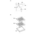
また、ゲート電極層401の側面にサイドウォール構造の側壁絶縁層を設けてもよい。ト
ランジスタ450は、ゲート電極層401の側面に膜厚の薄い側壁絶縁層412a、41
2bが設けられている。側壁絶縁層412a、412bは、ゲート電極層401を覆う絶
縁膜を形成した後、これをRIE(Reactive ion etching:反応性
イオンエッチング)法による異方性のエッチングによって絶縁膜を加工し、ゲート電極層
401の側壁に自己整合的にサイドウォール構造の側壁絶縁層412a、412bを形成
すればよい。ここで、絶縁膜について特に限定はないが、例えば、TEOS(Tetra
ethyl-Ortho-Silicate)若しくはシラン等と、酸素若しくは亜酸化
窒素等とを反応させて形成した段差被覆性のよい酸化シリコンを用いることができる。絶
縁膜は熱CVD、プラズマCVD、常圧CVD、バイアスECRCVD、スパッタリング
等の方法によって形成することができる。また、低温酸化(LTO:Low Tempe
rature Oxidation)法により形成する酸化シリコンを用いてもよい。A sidewall insulating layer having a sidewall structure may be provided on the side surface of the
2b is provided. The side
Silicon oxide, which has good step coverage and is formed by reacting silane or the like with oxygen or nitrous oxide, can be used. The insulating film can be formed by thermal CVD, plasma CVD, normal pressure CVD, bias ECRCVD, sputtering, or the like. In addition, low temperature oxidation (LTO: Low Temp.
Silicon oxide formed by a nature oxidation method may also be used.
側壁絶縁層412a、412bを設けることで、ゲート電極層401と低抵抗領域404
a、404bとのショートを防止することができる。By providing the
a and 404b can be prevented.
酸化物半導体層408a、408b全体にドーパントを導入して低抵抗領域とすると、酸
化物半導体層408a、408b下、酸化物絶縁層436側からも他の導電層と電気的接
続を行うことができる。When a dopant is introduced into the entire
酸化物半導体層403をインジウム、ガリウム、亜鉛、及び酸素の4元素を少なくとも含
み、該4元素の組成比を原子百分率で表したとき、インジウムの割合が、ガリウムの割合
及び亜鉛の割合の2倍以上である高い電界効果移動度のIGZO膜を用いて、膜厚を3~
5nmと薄くおさえることによってショートチャネル効果によるトランジスタのノーマリ
ーオンを防止することができる。When the
By keeping the thickness as thin as 5 nm, it is possible to prevent the transistor from normally-on due to the short channel effect.
酸化物半導体層408a、408bとしては、酸化インジウム、酸化スズ、酸化亜鉛、二
元系金属の酸化物であるIn-Zn系酸化物、Sn-Zn系酸化物、Al-Zn系酸化物
、Zn-Mg系酸化物、Sn-Mg系酸化物、In-Mg系酸化物、In-Ga系酸化物
、三元系金属の酸化物であるIn-Ga-Zn系酸化物(IGZOとも表記する)、In
-Al-Zn系酸化物、In-Sn-Zn系酸化物、Sn-Ga-Zn系酸化物、Al-
Ga-Zn系酸化物、Sn-Al-Zn系酸化物、In-Hf-Zn系酸化物、In-L
a-Zn系酸化物、In-Ce-Zn系酸化物、In-Pr-Zn系酸化物、In-Nd
-Zn系酸化物、In-Sm-Zn系酸化物、In-Eu-Zn系酸化物、In-Gd-
Zn系酸化物、In-Tb-Zn系酸化物、In-Dy-Zn系酸化物、In-Ho-Z
n系酸化物、In-Er-Zn系酸化物、In-Tm-Zn系酸化物、In-Yb-Zn
系酸化物、In-Lu-Zn系酸化物、四元系金属の酸化物であるIn-Sn-Ga-Z
n系酸化物、In-Hf-Ga-Zn系酸化物、In-Al-Ga-Zn系酸化物、In
-Sn-Al-Zn系酸化物、In-Sn-Hf-Zn系酸化物、In-Hf-Al-Z
n系酸化物を用いることができる。As the
-Al-Zn-based oxide, In-Sn-Zn-based oxide, Sn-Ga-Zn-based oxide, Al-
Ga-Zn-based oxide, Sn-Al-Zn-based oxide, In-Hf-Zn-based oxide, In-L
a-Zn oxide, In-Ce-Zn oxide, In-Pr-Zn oxide, In-Nd
-Zn-based oxide, In-Sm-Zn-based oxide, In-Eu-Zn-based oxide, In-Gd-
Zn-based oxide, In-Tb-Zn-based oxide, In-Dy-Zn-based oxide, In-Ho-Z
n-based oxide, In--Er--Zn-based oxide, In--Tm--Zn-based oxide, In--Yb--Zn
system oxide, In-Lu-Zn system oxide, In-Sn-Ga-Z which is a quaternary metal oxide
n-based oxide, In--Hf--Ga--Zn-based oxide, In--Al--Ga--Zn-based oxide, In
-Sn-Al-Zn-based oxide, In-Sn-Hf-Zn-based oxide, In-Hf-Al-Z
An n-type oxide can be used.
酸化物半導体層408a、408bとして、酸化インジウム、酸化スズ、酸化亜鉛のよう
な導電性の高い酸化物半導体層を用いてもよい。A highly conductive oxide semiconductor layer such as indium oxide, tin oxide, or zinc oxide may be used for the
本実施の形態では、酸化物半導体層408a、408bとして、インジウム:ガリウム:
亜鉛の組成比が1:1:1の酸化物ターゲットで作製された酸化物半導体層を用いる。In this embodiment, the
An oxide semiconductor layer formed using an oxide target with a composition ratio of zinc of 1:1:1 is used.
酸化物半導体層408a、408bの膜厚は20~50nmとすればよい。The thickness of the
トランジスタ450の作製方法の一例を図4(A)乃至(E)に示す。An example of a method for manufacturing the
まず、絶縁表面を有する基板400上に酸化物絶縁層436を形成し、酸化物絶縁層43
6上に酸化物半導体膜444を形成する(図4(A)参照)。本実施の形態では酸化物半
導体膜444をインジウム:ガリウム:亜鉛の組成比が1:1:1の酸化物ターゲットを
用いてスパッタリング法により形成する。First, the
An
次に酸化物半導体膜444をフォトリソグラフィ工程によって島状に加工し、一対の間隔
を有して設けられた酸化物半導体層408a、408bを形成する。酸化物半導体層40
8a、408b及び酸化物絶縁層436に接して酸化物半導体層403を形成する(図4
(B)参照)。酸化物半導体層403は、インジウム:ガリウム:亜鉛の組成比が3:1
:2の酸化物ターゲットを用いてスパッタリング法により形成する。酸化物半導体層40
3の端部はテーパーを有する形状が好ましく、本実施の形態では30度のテーパーを有す
る形状とする。Next, the
8a, 408b and the oxide insulating layer 436 (see FIG. 4).
(B)). The
: 2 by sputtering using an oxide target.
The end portion of 3 preferably has a shape having a taper, and in this embodiment, it has a shape having a taper of 30 degrees.
次いで、酸化物半導体層403上にゲート絶縁膜402、ゲート電極層401、ゲート電
極層401の側面を覆う側壁絶縁層412a、412bを形成する(図4(C)参照)。
ゲート絶縁膜402は酸化物半導体層403上に絶縁膜を形成し、該絶縁膜をゲート電極
層401及び側壁絶縁層412a、412bをマスクとしてエッチングすることで形成す
ることができる。なお、酸化物半導体層403の一部は露出する。Next, the
The
次いで、酸化物半導体層403、ソース電極層405a、ドレイン電極層405b、ゲー
ト絶縁膜402、ゲート電極層401上に、酸化物半導体層403の一部と接して、金属
元素を含む膜417を形成する(図1(C)参照)。Next, a
金属元素を含む膜417としては、金属膜、金属酸化物膜、金属窒化物膜等が挙げられる
。As the
金属元素を含む膜中の金属元素としては、アルミニウム(Al)、チタン(Ti)、モリ
ブデン(Mo)、タングステン(W)、ハフニウム(Hf)、タンタル(Ta)、ランタ
ン(La)、バリウム(Ba)、マグネシウム(Mg)、ジルコニウム(Zr)、及びニ
ッケル(Ni)のいずれかから選択される一以上を用いることができる。金属元素を含む
膜として、上記金属元素のいずれかから選択される一以上を含む金属膜、金属酸化物膜、
又は金属窒化物膜(例えば、窒化チタン膜、窒化モリブデン膜、窒化タングステン膜)を
用いることができる。また、金属元素を含む膜にリン(P)、ホウ素(B)などのドーパ
ントを含ませてもよい。本実施の形態において金属元素を含む膜417は導電性を有する
。The metal elements in the film containing metal elements include aluminum (Al), titanium (Ti), molybdenum (Mo), tungsten (W), hafnium (Hf), tantalum (Ta), lanthanum (La), barium (Ba). ), magnesium (Mg), zirconium (Zr), and nickel (Ni). As the film containing a metal element, a metal film containing one or more selected from any of the above metal elements, a metal oxide film,
Alternatively, a metal nitride film (eg, titanium nitride film, molybdenum nitride film, tungsten nitride film) can be used. Also, a film containing a metal element may contain a dopant such as phosphorus (P) or boron (B). In this embodiment mode, the
金属元素を含む膜417は、プラズマCVD法、スパッタリング法、又は蒸着法等により
成膜することができる。金属元素を含む膜417の膜厚は5nm以上30nm以下とすれ
ばよい。The
本実施の形態では、金属元素を含む膜417として膜厚10nmのアルミニウム膜をスパ
ッタリング法によって形成する。In this embodiment mode, an aluminum film with a thickness of 10 nm is formed by a sputtering method as the
次に、ゲート絶縁膜402、ゲート電極層401、及び側壁絶縁層412a、412bを
マスクとして、酸化物半導体層403に金属元素を含む膜417を通過してドーパント4
21を選択的に導入し、低抵抗領域を形成する(図4(D)参照)。Next, using the
21 is selectively introduced to form a low resistance region (see FIG. 4(D)).
ドーパント421は、酸化物半導体層403の導電率を変化させる不純物である。ドーパ
ント421としては、15族元素(代表的にはリン(P)、砒素(As)、およびアンチ
モン(Sb))、ホウ素(B)、アルミニウム(Al)、窒素(N)、アルゴン(Ar)
、ヘリウム(He)、ネオン(Ne)、インジウム(In)、フッ素(F)、塩素(Cl
)、チタン(Ti)、及び亜鉛(Zn)のいずれかから選択される一以上を用いることが
できる。A
, helium (He), neon (Ne), indium (In), fluorine (F), chlorine (Cl
), titanium (Ti), and zinc (Zn).
上記ドーパントは金属元素を含む膜417に含ませてもよい。The dopant may be contained in the
ドーパント421は、注入法により、金属元素を含む膜417を通過して、酸化物半導体
層403に導入する。ドーパント421の導入方法としては、イオン注入法、イオンドー
ピング法、プラズマイマージョンイオンインプランテーション法などを用いることができ
る。その際には、ドーパント421の単体のイオンあるいは水素化物やフッ化物、塩化物
のイオンを用いると好ましい。The
ドーパント421の導入工程は、加速電圧、ドーズ量などの注入条件、また通過させる金
属元素を含む膜417の膜厚を適宜設定して制御すればよい。例えば、ホウ素を用いて、
イオン注入法でホウ素イオンの注入を行う場合、加速電圧15kV、ドーズ量を1×10
15ions/cm2とすればよい。ドーズ量を1×1013ions/cm2以上5×
1016ions/cm2以下とすればよい。The step of introducing the
When boron ions are implanted by ion implantation, the acceleration voltage is 15 kV and the dose is 1×10.
15 ions/cm2 may be used. The dose amount is 1×10¹³ ions/cm2 or more 5×
It may be 1016 ions/cm2 or less.
低抵抗領域におけるドーパント421の濃度は、5×10¹⁸/cm3以上1×1022
/cm3以下であることが好ましい。The concentration of the
/cm3 or less.
ドーパントを導入する際に、基板400を加熱しながら行ってもよい。The dopant may be introduced while heating the
なお、酸化物半導体層403にドーパント421を導入する処理は、複数回行ってもよく
、ドーパントの種類も複数種用いてもよい。Note that the treatment for introducing the
また、ドーパント421の導入処理後、加熱処理を行ってもよい。加熱条件としては、温
度300℃以上700℃以下、好ましくは300℃以上450℃以下で1時間、酸素雰囲
気下で行うことが好ましい。また、窒素雰囲気下、減圧下、大気(超乾燥エア)下で加熱
処理を行ってもよい。Further, heat treatment may be performed after the introduction treatment of the
次に、金属元素を含む膜417及び酸化物半導体層403の一部が接した状態で加熱処理
を行う。加熱処理は酸素雰囲気下で行うことが好ましい。加熱処理は減圧下、窒素雰囲気
下でも行うことできる。また、加熱温度は100℃以上700℃以下、好ましくは200
℃以上400℃以下とすればよい。Next, heat treatment is performed while the
°C or higher and 400 °C or lower.
例えば、加熱処理装置の一つである電気炉に基板を導入し、金属元素を含む膜417及び
酸化物半導体層403に対して酸素雰囲気下200℃において1時間の加熱処理を行う。For example, the substrate is introduced into an electric furnace which is one of heat treatment apparatuses, and heat treatment is performed on the
なお、加熱処理装置は電気炉に限られず、抵抗発熱体などの発熱体からの熱伝導または熱
輻射によって、被処理物を加熱する装置を用いてもよい。例えば、GRTA(Gas R
apid Thermal Anneal)装置、LRTA(Lamp Rapid T
hermal Anneal)装置等のRTA(Rapid Thermal Anne
al)装置を用いることができる。LRTA装置は、ハロゲンランプ、メタルハライドラ
ンプ、キセノンアークランプ、カーボンアークランプ、高圧ナトリウムランプ、高圧水銀
ランプなどのランプから発する光(電磁波)の輻射により、被処理物を加熱する装置であ
る。GRTA装置は、高温のガスを用いて加熱処理を行う装置である。高温のガスには、
アルゴンなどの希ガス、または窒素のような、加熱処理によって被処理物と反応しない不
活性気体が用いられる。Note that the heat treatment apparatus is not limited to an electric furnace, and an apparatus that heats an object to be treated by heat conduction or heat radiation from a heating element such as a resistance heating element may be used. For example, GRTA (Gas R
apid Thermal Anneal) device, LRTA (Lamp Rapid T
RTA (rapid thermal anneal) such as a thermal anneal) device
al) the device can be used; An LRTA apparatus is an apparatus that heats an object by radiation of light (electromagnetic waves) emitted from lamps such as halogen lamps, metal halide lamps, xenon arc lamps, carbon arc lamps, high pressure sodium lamps, and high pressure mercury lamps. The GRTA apparatus is an apparatus that performs heat treatment using high-temperature gas. For hot gases,
A rare gas such as argon or an inert gas such as nitrogen that does not react with the object to be processed by heat treatment is used.
例えば、加熱処理として、650℃~700℃の高温に加熱した不活性ガス中に基板を入
れ、数分間加熱した後、基板を不活性ガス中から出すGRTAを行ってもよい。For example, as the heat treatment, GRTA may be performed in which the substrate is placed in an inert gas heated to a high temperature of 650° C. to 700° C., heated for several minutes, and then taken out of the inert gas.
加熱処理は、窒素、酸素、超乾燥空気(水の含有量が20ppm以下、好ましくは1pp
m以下、好ましくは10ppb以下の空気)、または希ガス(アルゴン、ヘリウムなど)
の雰囲気下で行えばよいが、上記窒素、酸素、超乾燥空気、または希ガス等の雰囲気に水
、水素などが含まれないことが好ましい。また、加熱処理装置に導入する窒素、酸素、ま
たは希ガスの純度を、6N(99.9999%)以上好ましくは7N(99.99999
%)以上(即ち不純物濃度を1ppm以下、好ましくは0.1ppm以下)とすることが
好ましい。The heat treatment is carried out using nitrogen, oxygen, ultra-dry air (with a water content of 20 ppm or less, preferably 1 pp).
m or less, preferably 10 ppb or less air), or noble gases (argon, helium, etc.)
However, it is preferable that the atmosphere of nitrogen, oxygen, ultra-dry air, rare gas, or the like does not contain water, hydrogen, or the like. Further, the purity of nitrogen, oxygen, or rare gas to be introduced into the heat treatment apparatus is 6N (99.9999%) or more, preferably 7N (99.99999%).
%) or more (that is, the impurity concentration is 1 ppm or less, preferably 0.1 ppm or less).
加熱処理により、金属元素を含む膜417から酸化物半導体層403へ金属元素が導入さ
れ、低抵抗領域414a、414bが形成される。よって酸化物半導体層403において
、チャネル形成領域409を挟んで、ドーパント及び金属元素を含む低抵抗領域414a
、414bが形成される。By the heat treatment, the metal element is introduced from the
, 414b are formed.
本実施の形態では、ドーパントとしてホウ素、金属元素としてアルミニウムを用いたため
、低抵抗領域414a、414bはホウ素及びアルミニウムを含む。Since boron is used as the dopant and aluminum is used as the metal element in this embodiment mode, the low-
次に金属元素を含む膜417をエッチングにより除去する。本実施の形態ではウェットエ
ッチング法により金属元素を含む膜417を除去する。Next, the
以上の工程で、本実施の形態のトランジスタ450が作製される。チャネル長方向にチャ
ネル形成領域409を挟んで低抵抗領域414a、414bを含む酸化物半導体層403
を有することにより、該トランジスタ450はオン特性(例えば、オン電流及び電界効果
移動度)が高く、高速動作、高速応答が可能となる。Through the above steps, the
, the
低抵抗領域414a、414bはソース領域、又はドレイン領域として機能させることが
できる。低抵抗領域414a、414bを設けることによって、低抵抗領域414a、4
14bの間に形成されるチャネル形成領域409に加わる電界を緩和させることができる
。また、低抵抗領域414a、414bにおいて酸化物半導体層403とソース電極層4
05a及びドレイン電極層405bとを電気的に接続させることによって、酸化物半導体
層403とソース電極層405a及びドレイン電極層405bとの接触抵抗を低減するこ
とができる。The
The electric field applied to the
05a and the
また、トランジスタ起因の表面凹凸を低減するために平坦化絶縁膜を形成してもよい。平
坦化絶縁膜としては、ポリイミド、アクリル、ベンゾシクロブテン系樹脂、等の有機材料
を用いることができる。また上記有機材料の他に、低誘電率材料(low-k材料)等を
用いることができる。なお、これらの材料で形成される絶縁膜を複数積層させることで、
平坦化絶縁膜を形成してもよい。Further, a planarization insulating film may be formed in order to reduce surface unevenness caused by the transistor. Organic materials such as polyimide, acryl, and benzocyclobutene-based resins can be used as the planarization insulating film. In addition to the above organic materials, low dielectric constant materials (low-k materials) and the like can be used. By stacking a plurality of insulating films made of these materials,
A planarization insulating film may be formed.
本実施の形態では、トランジスタ450上に平坦化絶縁膜415を形成する。また、平坦
化絶縁膜415に酸化物半導体層403達する開口を形成し、開口に酸化物半導体層40
3と電気的に接続するソース電極層405a、ドレイン電極層405bを形成する(図4
(E)参照)。In this embodiment, a
A
(E)).
以上のように、酸化物半導体をチャネル形成領域に用いたトランジスタの電気特性のしき
い値電圧をプラスにすることができ、所謂ノーマリーオフのスイッチング素子を実現する
トランジスタ構造およびその作製方法を提供することができる。As described above, a transistor structure in which the threshold voltage of electrical characteristics of a transistor using an oxide semiconductor for a channel formation region can be made positive and a so-called normally-off switching element is realized, and a manufacturing method thereof is provided. can do.
また、より高性能な半導体装置を実現するため、トランジスタのオン特性(例えば、オン
電流や電界効果移動度)を向上させて、半導体装置の高速応答、高速駆動を実現する構成
およびその作製方法を提供することができる。In addition, in order to realize a semiconductor device with higher performance, we will develop a structure and a manufacturing method for realizing high-speed response and high-speed driving of a semiconductor device by improving the on-characteristics (for example, on-current and field-effect mobility) of a transistor. can provide.
また、長期間の使用に際しても、しきい値電圧がシフトしにくく、信頼性の高い半導体装
置を提供することができる。In addition, it is possible to provide a highly reliable semiconductor device in which the threshold voltage is less likely to shift even when used for a long period of time.
本実施の形態は、他の実施の形態と適宜組み合わせて実施することが可能である。This embodiment can be implemented in appropriate combination with other embodiments.
(実施の形態3)
本実施の形態では、実施の形態1又は実施の形態2に示すトランジスタを使用し、電力が
供給されない状況でも記憶内容の保持が可能で、かつ、書き込み回数にも制限が無い半導
体装置の一例を、図面を用いて説明する。なお、本実施の形態の半導体装置は、トランジ
スタ162として実施の形態1又は実施の形態2に記載のトランジスタを適用して構成さ
れる。トランジスタ162としては、実施の形態1または2で示すトランジスタのいずれ
の構造も適用することができる。(Embodiment 3)
In this embodiment, an example of a semiconductor device which uses the transistor described in
トランジスタ162は、オフ電流が小さいため、これを用いることにより長期にわたり記
憶内容を保持することが可能である。つまり、リフレッシュ動作を必要としない、或いは
、リフレッシュ動作の頻度が極めて少ない半導体記憶装置とすることが可能となるため、
消費電力を十分に低減することができる。Since the
Power consumption can be sufficiently reduced.
図5は、半導体装置の構成の一例である。図5(A)に、半導体装置の断面図を、図5(
B)に半導体装置の平面図を、図5(C)に半導体装置の回路図をそれぞれ示す。ここで
、図5(A)は、図5(B)のC1-C2、及びD1-D2における断面に相当する。FIG. 5 shows an example of the configuration of a semiconductor device. FIG. 5A is a cross-sectional view of the semiconductor device, and FIG.
5B shows a plan view of a semiconductor device, and FIG. 5C shows a circuit diagram of the semiconductor device. Here, FIG. 5A corresponds to cross sections along C1-C2 and D1-D2 in FIG. 5B.
図5(A)及び図5(B)に示す半導体装置は、下部に第1の半導体材料を用いたトラン
ジスタ160を有し、上部に第2の半導体材料を用いたトランジスタ162を有するもの
である。トランジスタ162は、実施の形態1又は実施の形態2で示した構成と同一の構
成とすることができる。The semiconductor devices shown in FIGS. 5A and 5B have a
ここで、第1の半導体材料と第2の半導体材料は異なる禁制帯幅を持つ材料とすることが
望ましい。例えば、第1の半導体材料を酸化物半導体以外の半導体材料(シリコンなど)
とし、第2の半導体材料を酸化物半導体とすることができる。酸化物半導体以外の材料を
用いたトランジスタは、高速動作が容易である。一方で、酸化物半導体を用いたトランジ
スタは、その特性により長時間の電荷保持を可能とする。Here, it is desirable that the first semiconductor material and the second semiconductor material have different forbidden band widths. For example, the first semiconductor material is a semiconductor material other than an oxide semiconductor (such as silicon).
and the second semiconductor material can be an oxide semiconductor. A transistor using a material other than an oxide semiconductor can easily operate at high speed. On the other hand, a transistor including an oxide semiconductor can hold electric charge for a long time due to its characteristics.
なお、上記トランジスタは、いずれもnチャネル型トランジスタであるものとして説明す
るが、pチャネル型トランジスタを用いることができるのはいうまでもない。また、開示
する発明の技術的な本質は、情報を保持するために酸化物半導体をトランジスタ162に
用いる点にあるから、半導体装置に用いられる材料や半導体装置の構造など、半導体装置
の具体的な構成をここで示すものに限定する必要はない。Although the above transistors are all n-channel transistors, it goes without saying that p-channel transistors can also be used. In addition, since the technical essence of the disclosed invention is that an oxide semiconductor is used for the
図5(A)におけるトランジスタ160は、半導体材料(例えば、シリコンなど)を含む
基板185に設けられたチャネル形成領域116と、チャネル形成領域116を挟むよう
に設けられた不純物領域120と、不純物領域120に接する金属化合物領域124と、
チャネル形成領域116上に設けられたゲート絶縁層108と、ゲート絶縁層108上に
設けられたゲート電極110と、を有する。なお、図において、明示的にはソース電極や
ドレイン電極を有しない場合があるが、便宜上、このような状態を含めてトランジスタと
呼ぶ場合がある。また、この場合、トランジスタの接続関係を説明するために、ソース領
域やドレイン領域を含めてソース電極やドレイン電極と表現することがある。つまり、本
明細書において、ソース電極との記載には、ソース領域が含まれうる。A
A
基板185上にはトランジスタ160を囲むように素子分離絶縁層106が設けられてお
り、トランジスタ160を覆うように絶縁層130が設けられている。なお、高集積化を
実現するためには、図5(A)に示すようにトランジスタ160がサイドウォール絶縁層
を有しない構成とすることが望ましい。一方で、トランジスタ160の特性を重視する場
合には、ゲート電極110の側面にサイドウォール絶縁層を設け、不純物濃度が異なる領
域を含む不純物領域120としてもよい。An element
図5(A)に示すトランジスタ162は、酸化物半導体をチャネル形成領域に用いたトラ
ンジスタである。ここで、トランジスタ162に含まれる酸化物半導体層144は、高純
度化されたものであることが望ましい。高純度化された酸化物半導体を用いることで、極
めて優れたオフ特性のトランジスタ162を得ることができる。A
トランジスタ162上には、絶縁層150が単層または積層で設けられている。また、絶
縁層150を介して、トランジスタ162の電極層142aと重畳する領域には、導電層
148bが設けられており、電極層142aと、絶縁層150と、導電層148bとによ
って、容量素子164が構成される。すなわち、トランジスタ162の電極層142aは
、容量素子164の一方の電極として機能し、導電層148bは、容量素子164の他方
の電極として機能する。なお、容量が不要の場合には、容量素子164を設けない構成と
することもできる。また、容量素子164は、別途、トランジスタ162の上方に設けて
もよい。An insulating
トランジスタ162および容量素子164の上には絶縁層152が設けられている。そし
て、絶縁層152上にはトランジスタ162と、他のトランジスタを接続するための配線
156が設けられている。図5(A)には図示しないが、配線156は、絶縁層150、
絶縁層152及びゲート絶縁膜146などに形成された開口に形成された電極を介して電
極層142bと電気的に接続される。ここで、該電極は、少なくともトランジスタ162
の酸化物半導体層144の一部と重畳するように設けられることが好ましい。An insulating
It is electrically connected to the
It is preferably provided so as to overlap with part of the
図5(A)及び図5(B)において、トランジスタ160と、トランジスタ162とは、
少なくとも一部が重畳するように設けられており、トランジスタ160のソース領域また
はドレイン領域と酸化物半導体層144の一部が重畳するように設けられているのが好ま
しい。また、トランジスタ162及び容量素子164が、トランジスタ160の少なくと
も一部と重畳するように設けられている。例えば、容量素子164の導電層143bは、
トランジスタ160のゲート電極128と少なくとも一部が重畳して設けられている。こ
のような平面レイアウトを採用することにより、半導体装置の占有面積の低減を図ること
ができるため、高集積化を図ることができる。5A and 5B, the
They are provided so as to overlap at least partly, and preferably the source region or the drain region of the
At least part of it overlaps with the
なお、電極層142b及び配線156の電気的接続は、電極層142b及び配線156を
直接接触させて行ってもよいし、間の絶縁層に電極を設けて、該電極を介して行ってもよ
い。また、間に介する電極は、複数でもよい。The electrical connection between the
次に、図5(A)及び図5(B)に対応する回路構成の一例を図5(C)に示す。Next, FIG. 5C shows an example of a circuit configuration corresponding to FIGS. 5A and 5B.
図5(C)において、第1の配線(1st Line)とトランジスタ160のソース電
極とは、電気的に接続され、第2の配線(2nd Line)とトランジスタ160のド
レイン電極とは、電気的に接続されている。また、第3の配線(3rd Line)とト
ランジスタ162のソース電極またはドレイン電極の一方とは、電気的に接続され、第4
の配線(4th Line)と、トランジスタ162のゲート電極とは、電気的に接続さ
れている。そして、トランジスタ160のゲート電極と、トランジスタ162のソース電
極またはドレイン電極の一方は、容量素子164の電極の他方と電気的に接続され、第5
の配線(5th Line)と、容量素子164の電極の他方は電気的に接続されている
。In FIG. 5C, the first wiring (1st Line) and the source electrode of the
and the gate electrode of the
, and the other electrode of the
図5(C)に示す半導体装置では、トランジスタ160のゲート電極の電位が保持可能と
いう特徴を生かすことで、次のように、情報の書き込み、保持、読み出しが可能である。In the semiconductor device illustrated in FIG. 5C, the potential of the gate electrode of the
情報の書き込みおよび保持について説明する。まず、第4の配線の電位を、トランジスタ
162がオン状態となる電位にして、トランジスタ162をオン状態とする。これにより
、第3の配線の電位が、トランジスタ160のゲート電極、および容量素子164に与え
られる。すなわち、トランジスタ160のゲート電極には、所定の電荷が与えられる(書
き込み)。ここでは、異なる二つの電位レベルを与える電荷(以下Lowレベル電荷、H
ighレベル電荷という)のいずれかが与えられるものとする。その後、第4の配線の電
位を、トランジスタ162がオフ状態となる電位にして、トランジスタ162をオフ状態
とすることにより、トランジスタ160のゲート電極に与えられた電荷が保持される(保
持)。Describe writing and retention of information. First, the potential of the fourth wiring is set to a potential at which the
(referred to as the igh level charge). After that, the potential of the fourth wiring is set to a potential at which the
トランジスタ162のオフ電流は極めて小さいため、トランジスタ160のゲート電極の
電荷は長時間にわたって保持される。Since the off-state current of the
次に情報の読み出しについて説明する。第1の配線に所定の電位(定電位)を与えた状態
で、第5の配線に適切な電位(読み出し電位)を与えると、トランジスタ160のゲート
電極に保持された電荷量に応じて、第2の配線は異なる電位をとる。一般に、トランジス
タ160をnチャネル型とすると、トランジスタ160のゲート電極にHighレベル電
荷が与えられている場合の見かけのしきい値Vth_Hは、トランジスタ160のゲート
電極にLowレベル電荷が与えられている場合の見かけのしきい値Vth_Lより低くな
るためである。ここで、見かけのしきい値電圧とは、トランジスタ160を「オン状態」
とするために必要な第5の配線の電位をいうものとする。したがって、第5の配線の電位
をVth_HとVth_Lの中間の電位V0とすることにより、トランジスタ160のゲ
ート電極に与えられた電荷を判別できる。例えば、書き込みにおいて、Highレベル電
荷が与えられていた場合には、第5の配線の電位がV0(>Vth_H)となれば、トラ
ンジスタ160は「オン状態」となる。Lowレベル電荷が与えられていた場合には、第
5の配線の電位がV0(<Vth_L)となっても、トランジスタ160は「オフ状態」
のままである。このため、第2の配線の電位を見ることで、保持されている情報を読み出
すことができる。Next, reading of information will be described. When an appropriate potential (reading potential) is applied to the fifth wiring while a predetermined potential (constant potential) is applied to the first wiring, a 2 have different potentials. In general, if the
The potential of the fifth wiring required to achieve Therefore, the charge applied to the gate electrode of the
remains Therefore, the held information can be read by checking the potential of the second wiring.
なお、メモリセルをアレイ状に配置して用いる場合、所望のメモリセルの情報のみを読み
出せることが必要になる。このように情報を読み出さない場合には、ゲート電極の状態に
かかわらずトランジスタ160が「オフ状態」となるような電位、つまり、Vth_Hよ
り小さい電位を第5の配線に与えればよい。または、ゲート電極の状態にかかわらずトラ
ンジスタ160が「オン状態」となるような電位、つまり、Vth_Lより大きい電位を
第5の配線に与えればよい。Note that when memory cells are arranged in an array and used, it is necessary to be able to read only the information of a desired memory cell. In the case where data is not read as described above, a potential that turns off the
本実施の形態に示す半導体装置では、チャネル形成領域に酸化物半導体を用いたオフ電流
の極めて小さいトランジスタを適用することで、極めて長期にわたり記憶内容を保持する
ことが可能である。つまり、リフレッシュ動作が不要となるか、または、リフレッシュ動
作の頻度を極めて低くすることが可能となるため、消費電力を十分に低減することができ
る。また、電力の供給がない場合(ただし、電位は固定されていることが望ましい)であ
っても、長期にわたって記憶内容を保持することが可能である。In the semiconductor device described in this embodiment, memory data can be retained for an extremely long time by using a transistor including an oxide semiconductor for a channel formation region and having extremely low off-state current. In other words, the refresh operation becomes unnecessary or the frequency of the refresh operation can be extremely low, so that power consumption can be sufficiently reduced. In addition, memory contents can be retained for a long time even when power is not supplied (however, the potential is preferably fixed).
また、本実施の形態に示す半導体装置では、情報の書き込みに高い電圧を必要とせず、素
子の劣化の問題もない。例えば、従来の不揮発性メモリのように、フローティングゲート
への電子の注入や、フローティングゲートからの電子の引き抜きを行う必要がないため、
ゲート絶縁層の劣化といった問題が全く生じない。すなわち、開示する発明に係る半導体
装置では、従来の不揮発性メモリで問題となっている書き換え可能回数に制限はなく、信
頼性が飛躍的に向上する。さらに、トランジスタのオン状態、オフ状態によって、情報の
書き込みが行われるため、高速な動作も容易に実現しうる。In addition, the semiconductor device described in this embodiment mode does not require a high voltage for writing data, and there is no problem of element deterioration. For example, there is no need to inject electrons into the floating gate or extract electrons from the floating gate, unlike conventional nonvolatile memories.
Problems such as deterioration of the gate insulating layer do not occur at all. That is, in the semiconductor device according to the disclosed invention, there is no limitation on the number of rewritable times, which is a problem in conventional nonvolatile memories, and reliability is dramatically improved. Furthermore, high-speed operation can be easily achieved because information is written depending on whether the transistor is on or off.
また、トランジスタ162は、インジウム、ガリウム、亜鉛、及び酸素の4元素を少なく
とも含み、該4元素の組成比を原子百分率で表したとき、インジウムの割合が、ガリウム
の割合及び亜鉛の割合の2倍以上である酸化物半導体層を用いるため、しきい値電圧がプ
ラスであるトランジスタとすることができる。該トランジスタを採用することで、半導体
装置の高性能化を達成することができる。さらに、本実施の形態の半導体装置は、長期間
の使用に際しても、しきい値電圧がシフトしにくいトランジスタを用いるため、半導体装
置の高信頼性化を図ることができる。In addition, the
以上、本実施の形態に示す構成、方法などは、他の実施の形態に示す構成、方法などと適
宜組み合わせて用いることができる。The structures, methods, and the like described in this embodiment can be combined as appropriate with the structures, methods, and the like described in other embodiments.
(実施の形態4)
本実施の形態においては、実施の形態1又は実施の形態2に示すトランジスタを使用し、
電力が供給されない状況でも記憶内容の保持が可能で、かつ、書き込み回数にも制限が無
い半導体装置について、実施の形態3に示した構成と異なる構成について、図6及び図7
を用いて説明を行う。なお、本実施の形態の半導体装置は、トランジスタ162として実
施の形態1又は実施の形態2に記載のトランジスタを適用して構成される。トランジスタ
162としては、実施の形態1または2で示すトランジスタのいずれの構造も適用するこ
とができる。(Embodiment 4)
In this embodiment mode, the transistor described in
FIGS. 6 and 7 show structures different from the structure shown in
will be used for explanation. Note that the semiconductor device of this embodiment uses the transistor described in
図6(A)は、半導体装置の回路構成の一例を示し、図6(B)は半導体装置の一例を示
す概念図である。まず、図6(A)に示す半導体装置について説明を行い、続けて図6(
B)に示す半導体装置について、以下説明を行う。FIG. 6A illustrates an example of a circuit configuration of a semiconductor device, and FIG. 6B is a conceptual diagram illustrating an example of the semiconductor device. First, the semiconductor device shown in FIG. 6A will be described, followed by FIG.
The semiconductor device shown in B) will be described below.
図6(A)に示す半導体装置において、ビット線BLとトランジスタ162のソース電極
又はドレイン電極とは電気的に接続され、ワード線WLとトランジスタ162のゲート電
極とは電気的に接続され、トランジスタ162のソース電極又はドレイン電極と容量素子
254の第1の端子とは電気的に接続されている。In the semiconductor device in FIG. 6A, the bit line BL is electrically connected to the source or drain electrode of the
酸化物半導体を用いたトランジスタ162は、オフ電流が極めて小さいという特徴を有し
ている。このため、トランジスタ162をオフ状態とすることで、容量素子254の第1
の端子の電位(あるいは、容量素子254に蓄積された電荷)を極めて長時間にわたって
保持することが可能である。The
terminal (or charge accumulated in the capacitor 254) can be held for an extremely long time.
次に、図6(A)に示す半導体装置(メモリセル250)に、情報の書き込みおよび保持
を行う場合について説明する。Next, the case of writing and holding information in the semiconductor device (memory cell 250) illustrated in FIG. 6A is described.
まず、ワード線WLの電位を、トランジスタ162がオン状態となる電位として、トラン
ジスタ162をオン状態とする。これにより、ビット線BLの電位が、容量素子254の
第1の端子に与えられる(書き込み)。その後、ワード線WLの電位を、トランジスタ1
62がオフ状態となる電位として、トランジスタ162をオフ状態とすることにより、容
量素子254の第1の端子の電位が保持される(保持)。First, the potential of the word line WL is set to a potential at which the
62 is turned off, the potential of the first terminal of the
トランジスタ162のオフ電流は極めて小さいから、容量素子254の第1の端子の電位
(あるいは容量素子に蓄積された電荷)は長時間にわたって保持することができる。Since the off-state current of the
次に、情報の読み出しについて説明する。トランジスタ162がオン状態となると、浮遊
状態であるビット線BLと容量素子254とが導通し、ビット線BLと容量素子254の
間で電荷が再分配される。その結果、ビット線BLの電位が変化する。ビット線BLの電
位の変化量は、容量素子254の第1の端子の電位(あるいは容量素子254に蓄積され
た電荷)によって、異なる値をとる。Next, reading of information will be described. When the
例えば、容量素子254の第1の端子の電位をV、容量素子254の容量をC、ビット線
BLが有する容量成分(以下、ビット線容量とも呼ぶ)をCB、電荷が再分配される前の
ビット線BLの電位をVB0とすると、電荷が再分配された後のビット線BLの電位は、
(CB*VB0+C*V)/(CB+C)となる。従って、メモリセル250の状態とし
て、容量素子254の第1の端子の電位がV1とV0(V1>V0)の2状態をとるとす
ると、電位V1を保持している場合のビット線BLの電位(=(CB*VB0+C*V1
)/(CB+C))は、電位V0を保持している場合のビット線BLの電位(=(CB*
VB0+C*V0)/(CB+C))よりも高くなることがわかる。For example, the potential of the first terminal of the
(CB*VB0+C*V)/(CB+C). Therefore, assuming that the potential of the first terminal of the
)/(CB+C)) is the potential of the bit line BL when the potential V0 is held (=(CB*
VB0+C*V0)/(CB+C)).
そして、ビット線BLの電位を所定の電位と比較することで、情報を読み出すことができ
る。Information can be read by comparing the potential of the bit line BL with a predetermined potential.
このように、図6(A)に示す半導体装置は、トランジスタ162のオフ電流が極めて小
さいという特徴から、容量素子254に蓄積された電荷は長時間にわたって保持すること
ができる。つまり、リフレッシュ動作が不要となるか、または、リフレッシュ動作の頻度
を極めて低くすることが可能となるため、消費電力を十分に低減することができる。また
、電力の供給がない場合であっても、長期にわたって記憶内容を保持することが可能であ
る。As described above, the semiconductor device illustrated in FIG. 6A can hold charge accumulated in the
次に、図6(B)に示す半導体装置について、説明を行う。Next, the semiconductor device illustrated in FIG. 6B is described.
図6(B)に示す半導体装置は、上部に記憶回路として図6(A)に示したメモリセル2
50を複数有するメモリセルアレイ251a及び251bを有し、下部に、メモリセルア
レイ251(メモリセルアレイ251a及び251b)を動作させるために必要な周辺回
路253を有する。なお、周辺回路253は、メモリセルアレイ251と電気的に接続さ
れている。The semiconductor device shown in FIG. 6B has
It has
図6(B)に示した構成とすることにより、周辺回路253をメモリセルアレイ251(
メモリセルアレイ251a及び251b)の直下に設けることができるため半導体装置の
小型化を図ることができる。With the configuration shown in FIG. 6B, the
Since it can be provided directly under the
周辺回路253に設けられるトランジスタは、トランジスタ162とは異なる半導体材料
を用いるのがより好ましい。例えば、シリコン、ゲルマニウム、シリコンゲルマニウム、
炭化シリコン、またはガリウムヒ素等を用いることができ、単結晶半導体を用いることが
好ましい。他に、有機半導体材料などを用いてもよい。このような半導体材料を用いたト
ランジスタは、十分な高速動作が可能である。したがって、該トランジスタにより、高速
動作が要求される各種回路(論理回路、駆動回路など)を好適に実現することが可能であ
る。A semiconductor material different from that of the
Silicon carbide, gallium arsenide, or the like can be used, and a single crystal semiconductor is preferably used. Alternatively, an organic semiconductor material or the like may be used. A transistor using such a semiconductor material can operate at sufficiently high speed. Therefore, the transistor can be used to suitably implement various circuits (logic circuits, driver circuits, etc.) that require high-speed operation.
なお、図6(B)に示した半導体装置では、2つのメモリセルアレイ251(メモリセル
アレイ251aと、メモリセルアレイ251b)が積層された構成を例示したが、積層す
るメモリセルの数はこれに限定されない。3つ以上のメモリセルを積層する構成としても
良い。Note that although the semiconductor device in FIG. 6B illustrates a structure in which two memory cell arrays 251 (
次に、図6(A)に示したメモリセル250の具体的な構成について図7を用いて説明を
行う。Next, a specific structure of the
図7は、メモリセル250の構成の一例である。図7(A)に、メモリセル250の平面
図を、図7(B)に図7(A)の線分A-Bにおける断面図をそれぞれ示す。FIG. 7 shows an example of the configuration of the
図7(A)及び図7(B)に示すトランジスタ162は、実施の形態1又は実施の形態2
で示した構成と同一の構成とすることができる。The
It can be the same configuration as the configuration shown in .
図7(B)に示すように、電極502及び電極504上にトランジスタ162が設けられ
ている。電極502は、図6(A)におけるビット線BLとして機能する配線であり、ト
ランジスタ162の低抵抗領域と接して設けられている。また、電極504は、図6(A
)における容量素子254の一方の電極として機能し、トランジスタ162の低抵抗領域
と接して設けられている。トランジスタ162上において、電極504と重畳する領域に
設けられた電極506は、容量素子254の他方の電極として機能する。As shown in FIG. 7B, the
) and is provided in contact with the low-resistance region of the
また、図7(A)に示すように、容量素子254の他方の電極506は、容量線508と
電気的に接続する。ゲート絶縁膜146を介して酸化物半導体層144上に設けられたゲ
ート電極148aは、ワード線509と電気的に接続する。In addition, as shown in FIG. 7A, the
また、図7(C)に、メモリセルアレイ251と、周辺回路との接続部における断面図を
示す。周辺回路は、例えばnチャネル型トランジスタ510及びpチャネル型トランジス
タ512を含む構成とすることができる。nチャネル型トランジスタ510及びpチャネ
ル型トランジスタ512に用いる半導体材料としては、酸化物半導体以外の半導体材料(
シリコンなど)を用いるのが好ましい。このような材料を用いることで、周辺回路に含ま
れるトランジスタの高速動作を図ることができる。Further, FIG. 7C shows a cross-sectional view of a connection portion between the memory cell array 251 and a peripheral circuit. Peripheral circuitry may include, for example, an n-
silicon, etc.) is preferably used. By using such a material, high-speed operation of transistors included in the peripheral circuit can be achieved.
図7(A)に示す平面レイアウトを採用することにより、半導体装置の占有面積の低減を
図ることができるため、高集積化を図ることができる。By adopting the planar layout shown in FIG. 7A, the area occupied by the semiconductor device can be reduced, so that high integration can be achieved.
以上のように、上部に多層に形成された複数のメモリセルは、酸化物半導体を用いたトラ
ンジスタにより形成されている。インジウム、ガリウム、亜鉛、及び酸素の4元素を少な
くとも含み、該4元素の組成比を原子百分率で表したとき、インジウムの割合が、ガリウ
ムの割合及び亜鉛の割合の2倍以上である酸化物半導体を用いたトランジスタは、オフ電
流が小さいため、これを用いることにより長期にわたり記憶内容を保持することが可能で
ある。つまり、リフレッシュ動作の頻度を極めて低くすることが可能となるため、消費電
力を十分に低減することができる。また、容量素子254は、図7(B)で示すように電
極504、酸化物半導体層144、ゲート絶縁膜146、電極506が積層されることに
よって形成される。上記のような組成を有する酸化物半導体層の比誘電率は非常に高いた
め(比誘電率で66)、これを誘電体膜として用いることにより容量素子254が必要と
する面積を縮小することができる。As described above, the plurality of memory cells which are formed in multiple layers in the upper portion are formed of transistors using oxide semiconductors. An oxide semiconductor containing at least the four elements of indium, gallium, zinc, and oxygen, wherein the ratio of indium is at least twice the ratio of gallium and zinc when the composition ratio of the four elements is expressed as an atomic percentage. Since the off-state current of a transistor using .sub.2 is small, memory contents can be retained for a long time. In other words, the frequency of refresh operations can be extremely low, so power consumption can be sufficiently reduced. Further, the
このように、酸化物半導体以外の材料を用いたトランジスタ(換言すると、十分な高速動
作が可能なトランジスタ)を用いた周辺回路と、酸化物半導体を用いたトランジスタ(よ
り広義には、十分にオフ電流が小さいトランジスタ)を用いた記憶回路とを一体に備える
ことで、これまでにない特徴を有する半導体装置を実現することができる。また、周辺回
路と記憶回路を積層構造とすることにより、半導体装置の集積化を図ることができる。In this way, a peripheral circuit using a transistor using a material other than an oxide semiconductor (in other words, a transistor capable of sufficiently high-speed operation) and a transistor using an oxide semiconductor (in a broader sense, a sufficiently By integrally including a memory circuit using a transistor with a small current, a semiconductor device having unprecedented characteristics can be realized. Further, by forming the peripheral circuit and the memory circuit into a stacked structure, integration of the semiconductor device can be achieved.
本実施の形態は、他の実施の形態に記載した構成と適宜組み合わせて実施することが可能
である。This embodiment can be implemented in appropriate combination with any structure described in any of the other embodiments.
(実施の形態5)
本実施の形態では、先の実施の形態で示した半導体装置を携帯電話、スマートフォン、電
子書籍などの携帯機器に応用した場合の例を図8乃至図11を用いて説明する。(Embodiment 5)
In this embodiment, an example of applying the semiconductor device described in the above embodiment to a mobile device such as a mobile phone, a smart phone, or an e-book reader will be described with reference to FIGS.
携帯電話、スマートフォン、電子書籍などの携帯機器においては、画像データの一時記憶
などにSRAMまたはDRAMが使用されている。SRAMまたはDRAMが使用される
理由としてはフラッシュメモリでは応答が遅く、画像処理では不向きであるためである。
一方で、SRAMまたはDRAMを画像データの一時記憶に用いた場合、以下の特徴があ
る。2. Description of the Related Art Mobile devices such as mobile phones, smart phones, and electronic books use SRAMs or DRAMs for temporary storage of image data. The reason why SRAM or DRAM is used is that flash memory has a slow response and is unsuitable for image processing.
On the other hand, when SRAM or DRAM is used for temporary storage of image data, it has the following features.
通常のSRAMは、図8(A)に示すように1つのメモリセルがトランジスタ801~8
06の6個のトランジスタで構成されており、それをXデコーダー807、Yデコーダー
808にて駆動している。トランジスタ803とトランジスタ805、トランジスタ80
4とトランジスタ806はインバータを構成し、高速駆動を可能としている。しかし1つ
のメモリセルが6トランジスタで構成されているため、セル面積が大きいという欠点があ
る。デザインルールの最小寸法をFとしたときにSRAMのメモリセル面積は通常100
~150F2である。このためSRAMはビットあたりの単価が各種メモリの中で最も高
い。In a normal SRAM, one memory cell includes
06, which are driven by an X-decoder 807 and a Y-decoder 808 .
4 and
~150F2 . Therefore, SRAM has the highest unit price per bit among various memories.
それに対して、DRAMはメモリセルが図8(B)に示すようにトランジスタ811、保
持容量812によって構成され、それをXデコーダー813、Yデコーダー814にて駆
動している。1つのセルが1トランジスタ1容量の構成になっており、面積が小さい。D
RAMのメモリセル面積は通常10F2以下である。ただし、DRAMは常にリフレッシ
ュが必要であり、書き換えをおこなわない場合でも電力を消費する。On the other hand, a memory cell of a DRAM is composed of a
The memory cell area of RAM is usually 10 F2 or less. However, the DRAM always needs refreshing and consumes power even when it is not rewritten.
しかし、先の実施の形態で説明した半導体装置のメモリセル面積は、10F2前後であり
、且つ頻繁なリフレッシュは不要である。したがって、メモリセル面積が縮小され、且つ
消費電力が低減することができる。However, the memory cell area of the semiconductor device described in the previous embodiments is about10F2 , and frequent refreshing is unnecessary. Therefore, the memory cell area can be reduced and power consumption can be reduced.
図9に携帯機器のブロック図を示す。図9に示す携帯機器はRF回路901、アナログベ
ースバンド回路902、デジタルベースバンド回路903、バッテリー904、電源回路
905、アプリケーションプロセッサ906、フラッシュメモリ910、ディスプレイコ
ントローラ911、メモリ回路912、ディスプレイ913、タッチセンサ919、音声
回路917、キーボード918などより構成されている。ディスプレイ913は表示部9
14、ソースドライバ915、ゲートドライバ916によって構成されている。アプリケ
ーションプロセッサ906はCPU907、DSP908、インターフェイス909(I
F909)を有している。一般にメモリ回路912はSRAMまたはDRAMで構成され
ており、この部分に先の実施の形態で説明した半導体装置を採用することによって、情報
の書き込みおよび読み出しが高速で、長期間の記憶保持が可能で、且つ消費電力が十分に
低減することができる。FIG. 9 shows a block diagram of the mobile device. The mobile device shown in FIG. 9 includes an RF circuit 901, an analog baseband circuit 902, a digital baseband circuit 903, a battery 904, a power supply circuit 905, an application processor 906, a flash memory 910, a display controller 911, a memory circuit 912, a display 913, and a touch. It is composed of a sensor 919, an
14 , a source driver 915 and a gate driver 916 . Application processor 906 includes CPU 907, DSP 908, interface 909 (I
F909). In general, the memory circuit 912 is composed of an SRAM or a DRAM, and by employing the semiconductor device described in the previous embodiment for this portion, it is possible to write and read information at high speed and to retain data for a long period of time. , and the power consumption can be sufficiently reduced.
図10に、ディスプレイのメモリ回路950に先の実施の形態で説明した半導体装置を使
用した例を示す。図10に示すメモリ回路950は、メモリ952、メモリ953、スイ
ッチ954、スイッチ955およびメモリコントローラ951により構成されている。ま
た、メモリ回路950は、画像データ(入力画像データ)の信号線、メモリ952、及び
メモリ953に記憶されたデータ(記憶画像データ)を読み出し、及び制御を行うディス
プレイコントローラ956と、ディスプレイコントローラ956からの信号により表示す
るディスプレイ957が接続されている。FIG. 10 shows an example of using the semiconductor device described in the above embodiment for a memory circuit 950 of a display. A memory circuit 950 shown in FIG. The memory circuit 950 also includes a signal line for image data (input image data), a display controller 956 for reading and controlling data (stored image data) stored in the memory 952 and the memory 953, and A
まず、ある画像データがアプリケーションプロセッサ(図示しない)によって、形成され
る(入力画像データA)。入力画像データAは、スイッチ954を介してメモリ952に
記憶される。そしてメモリ952に記憶された画像データ(記憶画像データA)は、スイ
ッチ955、及びディスプレイコントローラ956を介してディスプレイ957に送られ
、表示される。First, some image data is formed (input image data A) by an application processor (not shown). Input image data A is stored in memory 952 via switch 954 . The image data (stored image data A) stored in the memory 952 is sent to the
入力画像データAに変更が無い場合、記憶画像データAは、通常30~60Hz程度の周
期でメモリ952からスイッチ955を介して、ディスプレイコントローラ956から読
み出される。When there is no change in the input image data A, the stored image data A is read from the memory 952 through the switch 955 and the display controller 956 at a cycle of about 30 to 60 Hz.
次に、例えばユーザーが画面を書き換える操作をしたとき(すなわち、入力画像データA
に変更が有る場合)、アプリケーションプロセッサは新たな画像データ(入力画像データ
B)を形成する。入力画像データBはスイッチ954を介してメモリ953に記憶される
。この間も定期的にメモリ952からスイッチ955を介して記憶画像データAは読み出
されている。メモリ953に新たな画像データ(記憶画像データB)が記憶し終わると、
ディスプレイ957の次のフレームより、記憶画像データBは読み出され、スイッチ95
5、及びディスプレイコントローラ956を介して、ディスプレイ957に記憶画像デー
タBが送られ、表示がおこなわれる。この読み出しはさらに次に新たな画像データがメモ
リ952に記憶されるまで継続される。Next, for example, when the user performs an operation to rewrite the screen (that is, input image data A
is changed), the application processor forms new image data (input image data B). Input image data B is stored in memory 953 via switch 954 . During this period, the stored image data A is periodically read out from the memory 952 via the switch 955 . When the new image data (stored image data B) is completely stored in the memory 953,
From the next frame on the
5 and the display controller 956, the stored image data B is sent to the
このようにメモリ952及びメモリ953は交互に画像データの書き込みと、画像データ
の読み出しを行うことによって、ディスプレイ957の表示をおこなう。なお、メモリ9
52及びメモリ953はそれぞれ別のメモリには限定されず、1つのメモリを分割して使
用してもよい。先の実施の形態で説明した半導体装置をメモリ952及びメモリ953に
採用することによって、情報の書き込みおよび読み出しが高速で、長期間の記憶保持が可
能で、且つ消費電力が十分に低減することができる。In this way, the memory 952 and the memory 953 alternately write image data and read image data, thereby performing display on the
52 and memory 953 are not limited to different memories, and one memory may be divided and used. By using the semiconductor device described in the above embodiment for the memory 952 and the memory 953, data can be written and read at high speed, data can be retained for a long time, and power consumption can be sufficiently reduced. can.
図11に電子書籍のブロック図を示す。図11はバッテリー1001、電源回路1002
、マイクロプロセッサ1003、フラッシュメモリ1004、音声回路1005、キーボ
ード1006、メモリ回路1007、タッチパネル1008、ディスプレイ1009、デ
ィスプレイコントローラ1010によって構成される。FIG. 11 shows a block diagram of an electronic book. FIG. 11 shows a battery 1001 and a power supply circuit 1002
, a microprocessor 1003 , a flash memory 1004 , an
ここでは、図11のメモリ回路1007に先の実施の形態で説明した半導体装置を使用す
ることができる。メモリ回路1007の役割は書籍の内容を一時的に保持する機能を持つ
。機能の例としては、ユーザーがハイライト機能を使用する場合などがある。ユーザーが
電子書籍を読んでいるときに、特定の箇所にマーキングをしたい場合がある。このマーキ
ング機能をハイライト機能と言い、表示の色を変える、アンダーラインを引く、文字を太
くする、文字の書体を変えるなどによって、周囲との違いを示すことである。ユーザーが
指定した箇所の情報を記憶し、保持する機能である。この情報を長期に保存する場合には
フラッシュメモリ1004にコピーしても良い。このような場合においても、先の実施の
形態で説明した半導体装置を採用することによって、情報の書き込みおよび読み出しが高
速で、長期間の記憶保持が可能で、且つ消費電力が十分に低減することができる。Here, the semiconductor device described in the above embodiment can be used for the memory circuit 1007 in FIG. The role of the memory circuit 1007 is to temporarily hold the contents of the book. An example of a feature is when a user uses a highlight feature. When a user is reading an e-book, there are cases where he/she wants to mark a specific part. This marking function is called a highlighting function, and is to indicate the difference from the surroundings by changing the display color, drawing an underline, thickening the characters, changing the typeface of the characters, and the like. This is a function to store and hold information specified by the user. If this information is to be stored for a long period of time, it may be copied to the flash memory 1004 . Even in such a case, by employing the semiconductor device described in any of the above embodiments, data can be written and read at high speed, memory can be retained for a long time, and power consumption can be sufficiently reduced. can be done.
以上のように、本実施の形態に示す携帯機器には、先の実施の形態に係る半導体装置が搭
載されている。このため、読み出しが高速で、長期間の記憶保持が可能で、且つ消費電力
を低減した携帯機器が実現される。As described above, the portable device described in this embodiment includes the semiconductor device according to any of the above embodiments. Therefore, it is possible to realize a portable device that can read data at high speed, can retain data for a long period of time, and consumes less power.
本実施の形態に示す構成、方法などは、他の実施の形態に示す構成、方法などと適宜組み
合わせて用いることができる。The structures, methods, and the like described in this embodiment can be combined as appropriate with the structures, methods, and the like described in other embodiments.
本実施例では、インジウム、ガリウム、及び亜鉛を含む酸化物半導体膜(IGZO膜)を
作製し、酸化物半導体膜のイオン化ポテンシャルの測定を行い、その結果に基づきエネル
ギーバンド図を計算した。本明細書において、イオン化ポテンシャルの値は、バンドギャ
ップ(エネルギーギャップ)と電子親和力を加算した値であり、バンドギャップの値は、
材料の単膜の分光エリプソメトリーで測定して得られる値を用いる。また、酸化物半導体
膜の組成分析を行った。In this example, an oxide semiconductor film (IGZO film) containing indium, gallium, and zinc was formed, the ionization potential of the oxide semiconductor film was measured, and an energy band diagram was calculated based on the measurement result. In this specification, the ionization potential value is the sum of the bandgap (energy gap) and the electron affinity, and the bandgap value is
A value obtained by spectroscopic ellipsometry measurement of a single film of material is used. In addition, composition analysis of the oxide semiconductor film was performed.
まず、分光エリプソメトリーで測定して得られたバンドギャップの結果を示す。First, the bandgap results obtained by spectroscopic ellipsometry are shown.
試料となる酸化物半導体膜として、石英基板上にスパッタリング法を用いて膜厚100n
mのIGZO膜を成膜した。成膜条件は、基板温度を300℃とし、ターゲットとしては
、In:Ga:Zn=3:1:2[原子数比]の酸化物ターゲットを用いた。As an oxide semiconductor film to be a sample, a film having a thickness of 100 nm was formed on a quartz substrate using a sputtering method.
An IGZO film with a thickness of m was deposited. The deposition conditions were such that the substrate temperature was 300° C., and an oxide target of In:Ga:Zn=3:1:2 [atomic ratio] was used as the target.
バンドギャップは、アルゴン及び酸素(アルゴン:酸素=30sccm:15sccm)
雰囲気下において成膜し、成膜後熱処理なしの試料では2.83eV、成膜後450℃で
熱処理(窒素雰囲気下で1時間の後、酸素雰囲気下で1時間)した試料は2.90eV、
成膜後650℃熱処理(窒素雰囲気下で1時間の後、酸素雰囲気下で1時間)した試料は
2.94eV、また、酸素雰囲気(酸素100%)下において成膜し、成膜後熱処理なし
の試料では2.82eV、成膜後450℃熱処理(窒素雰囲気下で1時間の後、酸素雰囲
気下で1時間)した試料は2.89eV、成膜後650℃熱処理(窒素雰囲気下で1時間
の後、酸素雰囲気下で1時間)した試料は2.94eVであり、約2.8eV~2.9e
Vであった。The bandgap is argon and oxygen (argon:oxygen=30sccm:15sccm)
2.83 eV for a sample without heat treatment after film formation, 2.90 eV for a sample after heat treatment at 450° C. (after 1 hour in a nitrogen atmosphere and 1 hour in an oxygen atmosphere) after film formation,
A sample subjected to heat treatment at 650° C. after film formation (1 hour in nitrogen atmosphere, then 1 hour in oxygen atmosphere) has 2.94 eV. 2.82 eV for the sample, and 2.89 eV for the sample heat-treated at 450°C after film formation (one hour in nitrogen atmosphere, then one hour in oxygen atmosphere), and 2.89 eV after film-formation heat treatment at 650°C (one hour in nitrogen atmosphere). After that, the sample that has been left in an oxygen atmosphere for 1 hour has a value of 2.94 eV, which is about 2.8 eV to 2.9 eV.
was V.
また、単結晶シリコン基板上に、酸素雰囲気(酸素100%)下、基板温度300℃、I
n:Ga:Zn=3:1:2[原子数比]の酸化物ターゲットを用いたスパッタリング法
により膜厚15nmで成膜して得られたIGZO膜を、該膜の表面側からスパッタリング
しながら紫外線光電子分光分析(UPS:Ultraviolet Photoelec
tron Spctroscopy)によるイオン化ポテンシャルを測定した。なお、イ
オン化ポテンシャルは真空準位から価電子帯までのエネルギー差を表す。In addition, on a single crystal silicon substrate, in an oxygen atmosphere (oxygen 100%), a substrate temperature of 300° C., I
An IGZO film obtained by forming a film with a thickness of 15 nm by a sputtering method using an oxide target of n:Ga:Zn=3:1:2 [atomic ratio] was sputtered from the surface side of the film. Ultraviolet photoelectron spectroscopy (UPS: Ultraviolet Photoelec
The ionization potential was measured by tron Spectroscopy). Note that the ionization potential represents the energy difference from the vacuum level to the valence band.
イオン化ポテンシャルの値から分光エリプソメトリーで測定したバンドギャップを引くこ
とで伝導帯のエネルギーを算出し、この、In:Ga:Zn=3:1:2[原子数比]の
酸化物ターゲットを用いて成膜したIGZO膜のバンド構造を作成した。ただし、IGZ
O膜のバンドギャップは2.8eVとした。その結果が図12となる。The conduction band energy was calculated by subtracting the bandgap measured by spectroscopic ellipsometry from the value of the ionization potential, and using this In:Ga:Zn=3:1:2 [atomic ratio] oxide target A band structure of the deposited IGZO film was created. However, IGZ
The bandgap of the O film was set to 2.8 eV. The result is shown in FIG.
次に、単結晶シリコン基板上に、酸素雰囲気(酸素100%)下、基板温度300℃、I
n:Ga:Zn=3:1:2[原子数比]の酸化物ターゲットを用いたスパッタリング法
により膜厚15nmで成膜して得られたIGZO膜の組成をX線光電子分光法(XPS:
X-ray Photoelectron Spectroscopy)分析によって定
量化して評価した。Next, on the single crystal silicon substrate, in an oxygen atmosphere (oxygen 100%), a substrate temperature of 300° C., I
The composition of an IGZO film obtained by forming a 15 nm-thickness IGZO film by sputtering using an oxide target of n:Ga:Zn=3:1:2 [atomic ratio] was analyzed by X-ray photoelectron spectroscopy (XPS:
quantified and evaluated by X-ray Photoelectron Spectroscopy) analysis.
IGZO膜において、インジウム(In)が23.7atomic%、ガリウム(Ga)
が7.5atomic%、亜鉛(Zn)が9atomic%、酸素(O)が59.7at
omic%であった。In the IGZO film, indium (In) is 23.7 atomic % and gallium (Ga)
is 7.5 atomic %, zinc (Zn) is 9 atomic %, and oxygen (O) is 59.7 atomic %
was omic%.
また、In:Ga:Zn=3:1:2[原子数比]の酸化物ターゲットを用いて成膜した
IGZO膜のX線回折(XRD:X-Ray Diffraction)測定を行った。In addition, an X-ray diffraction (XRD) measurement of an IGZO film formed using an oxide target of In:Ga:Zn=3:1:2 [atomic ratio] was performed.
試料として、石英基板上にスパッタリング法を用いて膜厚100nmのIGZO膜を成膜
した。成膜条件は、基板温度を室温、200℃、300℃、又は400℃とし、成膜雰囲
気をアルゴン及び酸素(アルゴン:酸素=30sccm:15sccm)とし、ターゲッ
トとして、In:Ga:Zn=3:1:2[原子数比]の酸化物ターゲットを用いた。As a sample, an IGZO film with a thickness of 100 nm was formed over a quartz substrate by a sputtering method. The film formation conditions were such that the substrate temperature was room temperature, 200° C., 300° C., or 400° C., the film formation atmosphere was argon and oxygen (argon:oxygen=30 sccm:15 sccm), and the targets were In:Ga:Zn=3: A 1:2 [atomic ratio] oxide target was used.
それぞれのIGZO膜についてout-of-plane法を用いてXRDスペクトルを
測定した結果を図13に示す。図13において、縦軸はx線回折強度(任意単位)であり
、横軸は回転角2θ(deg.)である。なお、XRDスペクトルの測定は、Bruke
r AXS社製X線回折装置D8 ADVANCEを用いた。FIG. 13 shows the result of measuring the XRD spectrum of each IGZO film using the out-of-plane method. In FIG. 13, the vertical axis is the x-ray diffraction intensity (arbitrary unit), and the horizontal axis is the rotation angle 2θ (deg.). It should be noted that the measurement of the XRD spectrum, Bruke
An X-ray diffractometer D8 ADVANCE manufactured by rAXS was used.
図13に示すように、室温で成膜したIGZO膜は、XRDスペクトルでは結晶を示すピ
ークが見られず非晶質酸化物半導体膜であることが確認できた。また、200℃、300
℃、又は400℃で成膜したIGZO膜は、図13に示すようにXRDスペクトルにおい
て、2θ=31°近傍に、結晶に起因するピークが見られ、結晶性酸化物半導体膜である
ことが確認できた。As shown in FIG. 13, it was confirmed that the IGZO film formed at room temperature was an amorphous oxide semiconductor film because no peak indicating crystals was observed in the XRD spectrum. Also, 200°C, 300°C
As shown in FIG. 13, the IGZO film deposited at 400° C. or 400° C. has a peak attributed to crystals near 2θ=31° in the XRD spectrum, confirming that it is a crystalline oxide semiconductor film. did it.
次にIGZO膜の端面を切り出し、高分解能透過電子顕微鏡(日立ハイテクノロジー製「
H9000-NAR」:TEM)で加速電圧を300kVとし、IGZO膜の断面観察を
行った。Next, the end face of the IGZO film was cut out and subjected to a high-resolution transmission electron microscope (manufactured by Hitachi High Technology "
H9000-NAR": TEM) at an accelerating voltage of 300 kV, and the cross section of the IGZO film was observed.
試料として、石英基板上にスパッタリング法を用いて膜厚100nmのIGZO膜を成膜
した。成膜条件は、基板温度を300℃、成膜雰囲気をアルゴン及び酸素(アルゴン:酸
素=30sccm:15sccm)とし、ターゲットとして、In:Ga:Zn=3:1
:2[原子数比]の酸化物ターゲットを用いた。As a sample, an IGZO film with a thickness of 100 nm was formed over a quartz substrate by a sputtering method. The film formation conditions were a substrate temperature of 300° C., a film formation atmosphere of argon and oxygen (argon:oxygen=30 sccm:15 sccm), and a target of In:Ga:Zn=3:1.
: An oxide target of 2 [atomic number ratio] was used.
図16(A)に成膜後加熱処理なし、図16(B)に成膜後450℃熱処理(窒素雰囲気
下1時間の後、酸素雰囲気下1時間)、図16(C)に成膜後650℃熱処理(窒素雰囲
気下1時間の後、酸素雰囲気下1時間)のIGZO膜の断面におけるTEM像を示す。FIG. 16A shows no heat treatment after film formation, FIG. 16B shows heat treatment at 450° C. after film formation (after 1 hour in nitrogen atmosphere, 1 hour in oxygen atmosphere), and FIG. 16C shows after film formation. 1 shows a TEM image of a cross-section of an IGZO film subjected to heat treatment at 650° C. (after 1 hour under nitrogen atmosphere, then 1 hour under oxygen atmosphere).
図16(A)乃至(C)に示すように、表面に概略垂直なc軸を有している結晶(CAA
C)を含むIGZO膜が確認できた。As shown in FIGS. 16A to 16C, crystals (CAA
An IGZO film containing C) was confirmed.
以上のように、In:Ga:Zn=3:1:2[原子数比]の酸化物ターゲットを用いて
非単結晶のIGZO膜が得られることが確認できた。As described above, it was confirmed that a non-single-crystal IGZO film can be obtained using an oxide target of In:Ga:Zn=3:1:2 [atomic ratio].
本実施例では、In:Ga:Zn=3:1:2[原子数比]の酸化物ターゲットを用いて
成膜されたIGZO膜を有するトランジスタを作製し、電気特性及び信頼性の評価を行っ
た。In this example, a transistor having an IGZO film formed using an oxide target of In:Ga:Zn=3:1:2 [atomic ratio] was manufactured, and electrical characteristics and reliability were evaluated. rice field.
トランジスタとして、図1に示すトランジスタ440aの構造のトランジスタ1、及び図
2(A)に示すトランジスタ440bの構造のトランジスタ2を作製した。以下にトラン
ジスタ1及びトランジスタ2の作製方法を示す。As transistors, a
ガラス基板上に絶縁層としてスパッタリング法を用いて、膜厚300nmの酸化シリコン
膜を形成した(成膜条件:酸素雰囲気下、圧力0.4Pa、電源1.5kW、ガラス基板
とターゲットとの間の距離を60mm、基板温度100℃)。A silicon oxide film with a thickness of 300 nm was formed as an insulating layer on a glass substrate using a sputtering method (film formation conditions: oxygen atmosphere, pressure 0.4 Pa, power supply 1.5 kW, distance between the glass substrate and the
酸化シリコン膜表面を研磨処理後、酸化物半導体膜としてIn:Ga:Zn=3:1:2
[原子数比]の酸化物ターゲットを用いたスパッタリング法により、膜厚20nmのIG
ZO膜を形成した。成膜条件は、アルゴン及び酸素(アルゴン:酸素=30sccm:1
5sccm)雰囲気下、圧力0.4Pa、電源1.5kW、ガラス基板とターゲットとの
間の距離を60mm、基板温度200℃とした。After the surface of the silicon oxide film was polished, In:Ga:Zn=3:1:2 as an oxide semiconductor film.
An IG with a film thickness of 20 nm was formed by a sputtering method using an oxide target with [atomic ratio].
A ZO film was formed. The film formation conditions are argon and oxygen (argon: oxygen = 30 sccm: 1
5 sccm) atmosphere, a pressure of 0.4 Pa, a power source of 1.5 kW, a distance between the glass substrate and the target of 60 mm, and a substrate temperature of 200°C.
次に、温度450℃、窒素雰囲気下1時間の熱処理後、酸素雰囲気下1時間の熱処理を行
った。IGZO膜をICP(Inductively Coupled Plasma:
誘導結合型プラズマ)エッチング法により、エッチング(エッチング条件:エッチングガ
ス(BCl3:Cl2=60sccm:20sccm)、電源電力450W、バイアス電
力100W、圧力1.9Pa)し、島状に加工した。Next, after heat treatment at a temperature of 450° C. for 1 hour in a nitrogen atmosphere, heat treatment was performed in an oxygen atmosphere for 1 hour. ICP (Inductively Coupled Plasma:
Etching (etching conditions: etching gas (BCl3 :Cl2 =60 sccm:20 sccm), power supply power 450 W, bias power 100 W, pressure 1.9 Pa) was performed by an inductively coupled plasma etching method to form islands.
スパッタリング法により膜厚50nmのタングステン膜(成膜条件:アルゴン雰囲気下、
圧力0.8Pa、電源電力1kW)を成膜し、ICPエッチング法により、エッチング(
エッチング条件:エッチングガス(CF4:Cl2:O2=25sccm:25sccm
:10sccm)、電源電力500W、バイアス電力150W、圧力1.0Pa)してソ
ース電極層及びドレイン電極層を形成した。A tungsten film with a thickness of 50 nm is formed by a sputtering method (film formation conditions: under an argon atmosphere,
pressure 0.8 Pa,
Etching conditions: etching gas (CF4 :Cl2 :O2 =25 sccm:25 sccm
: 10 sccm), power source power 500 W, bias power 150 W, pressure 1.0 Pa) to form a source electrode layer and a drain electrode layer.
次にCVD法により酸化窒化シリコン膜を30nm成膜し、ゲート絶縁膜を形成した。Next, a silicon oxynitride film of 30 nm was formed by a CVD method to form a gate insulating film.
スパッタリング法により膜厚15nmの窒化タンタル膜(成膜条件:アルゴン及び窒素(
Ar:N2=50sccm:10sccm)雰囲気下、圧力0.6Pa、電源電力1kW
)及び膜厚135nmのタングステン膜(成膜条件:アルゴン雰囲気下、圧力2.0Pa
、電源電力4kW)の積層を成膜し、エッチング法により、エッチング(第1エッチング
条件:エッチングガス(Cl2:SF6:O2=33sccm:33sccm:10sc
cm、電源電力2000W、バイアス電力50W、圧力0.67Pa)(第2エッチング
条件:エッチングガス(Cl2=100sccm、電源電力2000W、バイアス電力5
0W、圧力0.67Pa)してゲート電極層を形成した。A tantalum nitride film with a thickness of 15 nm is formed by a sputtering method (film formation conditions: argon and nitrogen (
Ar: N2 = 50 sccm: 10 sccm) atmosphere, pressure 0.6 Pa,
) and a tungsten film with a film thickness of 135 nm (film formation conditions: argon atmosphere, pressure 2.0 Pa
,
cm, power supply power 2000 W, bias power 50 W, pressure 0.67 Pa) (Second etching conditions: etching gas (Cl2 =100 sccm, power supply power 2000 W, bias power 5
0 W, pressure 0.67 Pa) to form a gate electrode layer.
トランジスタ1のみ、ゲート電極層、ソース電極層及びドレイン電極層をマスクとしてイ
オン注入法によりIGZO膜に、リン(P)イオンを注入した。なお、リン(P)イオン
の注入条件は加速電圧40kV、ドーズ量を1.0×10¹⁵ions/cm2とした。For only the
絶縁膜としてゲート電極層上に、スパッタリング法により酸化アルミニウム膜(成膜条件
:アルゴン及び酸素(アルゴン:酸素=25sccm:25sccm)雰囲気下、圧力0
.4Pa、電源電力2.5kW、ガラス基板とターゲットとの間の距離を60mm、基板
温度250℃)を成膜し、CVD法により酸化窒化シリコン膜を300nm積層した。As an insulating film, an aluminum oxide film (film formation conditions: argon and oxygen (argon:oxygen=25 sccm:25 sccm) atmosphere under a pressure of 0 is formed on the gate electrode layer by a sputtering method.
. 4 Pa, power supply power of 2.5 kW, distance between glass substrate and target of 60 mm, substrate temperature of 250° C.), and a silicon oxynitride film of 300 nm was deposited by CVD.
次に、ゲート絶縁膜及び絶縁膜にIGZO膜に達する開口を形成し、該開口にスパッタリ
ング法により膜厚50nmのチタン膜(成膜条件:アルゴン(Ar=20sccm)雰囲
気下、圧力0.1Pa、電源電力12kW)、膜厚100nmのアルミニウム膜(成膜条
件:アルゴン(Ar=50sccm)雰囲気下、圧力0.4Pa、電源電力1kW)、膜
厚50nmのチタン膜(成膜条件:アルゴン(Ar=20sccm)雰囲気下、圧力0.
1Pa、電源電力12kW)の積層を成膜し、エッチング(エッチング条件:エッチング
ガス(BCl3:Cl2=60sccm:20sccm)、電源電力450W、バイアス
電力100W、圧力1.9Pa)して、配線層を形成した。Next, an opening reaching the IGZO film is formed in the gate insulating film and the insulating film, and a titanium film having a thickness of 50 nm is formed in the opening by a sputtering method (film formation conditions: argon (Ar=20 sccm) atmosphere, pressure 0.1 Pa,
1 Pa,
以上の工程でトランジスタ1及びトランジスタ2を作製した。なお、トランジスタ1にお
いては、チャネル長(L)は3.2μm及びチャネル幅(W)は10.1μm、酸化物半
導体膜上においてソース電極層、ドレイン電極層、及びゲート電極層のどれとも重ならな
い領域のチャネル長方向の幅(Loffともいう)は0.15μmとした。一方、なお、
トランジスタ2においては、チャネル長(L)は2.9μm及びチャネル幅(W)は10
.1μm、酸化物半導体膜上においてソース電極層又はドレイン電極層がゲート電極層と
重なる領域のチャネル長方向の幅(Lovともいう)は1.15μmとした。Through the above steps, the
In
. The width (also referred to as Lov) in the channel length direction of the region where the source electrode layer or the drain electrode layer overlaps with the gate electrode layer over the oxide semiconductor film was 1.15 μm.
得られたトランジスタ1及びトランジスタ2の電気特性、及びトランジスタ1においては
信頼性評価も行った。トランジスタ2のドレイン電圧(Vd)が3V、0.1Vにおける
ゲート電圧(Vg)-ドレイン電流(Id)特性、及びドレイン電圧(Vd)が0.1V
における電界効果移動度を図14に、トランジスタ1のドレイン電圧(Vd)が3V、0
.1Vにおけるゲート電圧(Vg)-ドレイン電流(Id)特性、及びドレイン電圧(V
d)が0.1Vにおける電界効果移動度を図15(A)(B)に示す。Electrical characteristics of the obtained
14, the drain voltage (Vd) of the
. Gate voltage (Vg)-drain current (Id) characteristics at 1 V and drain voltage (V
15(A) and 15(B) show the field effect mobility at 0.1 V in d).
図14及び図15に示すようにトランジスタ1及びトランジスタ2は、高いオン特性を示
し、電界効果移動度は20cm2/Vs付近であり、トランジスタ2においては20cm
2/Vsを超える電界効果移動度であった。As shown in FIGS. 14 and 15, the
The field effect mobility exceeded2 /Vs.
トランジスタの信頼性を調べるための手法の一つに、バイアス-熱ストレス試験(以下、
GBT(Gate Bias Temperature)試験と呼ぶ。)がある。GBT
試験は加速試験の一種であり、長期間の使用によって起こるトランジスタの特性変化を、
短時間で評価することができる。特に、GBT試験前後におけるトランジスタのしきい値
電圧の変化量は、信頼性を調べるための重要な指標となる。GBT試験前後において、し
きい値電圧の変化量が小さいほど信頼性が高い。Bias-thermal stress test (hereinafter referred to as
It is called a GBT (Gate Bias Temperature) test. ). GBT
The test is a type of accelerated test, and the changes in transistor characteristics caused by long-term use are
It can be evaluated in a short time. In particular, the amount of change in the threshold voltage of the transistor before and after the GBT test is an important index for examining reliability. Before and after the GBT test, the smaller the amount of change in threshold voltage, the higher the reliability.
トランジスタが形成されている基板を一定の温度に維持し、トランジスタのソースとドレ
インを同電位とし、ゲートにはソース及びドレインとは異なる電位を一定時間与える。基
板の温度は、試験目的に応じて適宜設定すればよい。なお、「+GBT試験」では、ゲー
トに与える電位がソース及びドレインの電位(ソースとドレインは同電位である。)より
も高く、「-GBT試験」では、ゲートに与える電位がソース及びドレインの電位(ソー
スとドレインは同電位である。)よりも低い。The substrate on which the transistor is formed is maintained at a constant temperature, the source and drain of the transistor are set at the same potential, and the gate is applied with a potential different from that of the source and drain for a predetermined period of time. The temperature of the substrate may be appropriately set according to the purpose of the test. In the "+GBT test", the potential applied to the gate is higher than the potential of the source and drain (the source and drain are the same potential), and in the "-GBT test", the potential applied to the gate is the potential of the source and drain. (source and drain are at the same potential).
GBT試験の試験強度は、基板温度、ゲート絶縁層に加えられる電界強度及び電界印加時
間により決定することができる。ゲート絶縁層中の電界強度は、ゲートと、ソース及びド
レインと、の間の電位差をゲート絶縁層の厚さで除して決定される。The test strength of the GBT test can be determined by the substrate temperature, the electric field strength applied to the gate insulating layer, and the electric field application time. The electric field strength in the gate insulating layer is determined by the potential difference between the gate and the source and drain divided by the thickness of the gate insulating layer.
本実施例ではトランジスタ1にGBT試験を行った。まず+GBT試験として、基板温度
を40℃とし、Vdを3Vとし、トランジスタ1のVg-Id特性の測定を行った。次に
、基板温度を150℃とし、Vdを0.1Vとした。次に、ゲート絶縁膜に印加される電
界強度が2MV/cmとなるようにVgに6Vを印加し、そのまま大気雰囲気下で1時間
保持した。次に、Vgを0Vとした。次に、基板温度40℃とし、Vdを10Vとし、ト
ランジスタ1のVg-Id測定を行った。+GBT試験結果を図15(A)に示す。In this example, a GBT test was performed on the
同様に、-GBT試験まず基板温度を40℃とし、V(ds)を10Vとし、トランジス
タ1のVg-Id特性の測定を行った。次に、基板温度を150℃とし、Vdを0.1V
とした。次に、ゲート絶縁膜に印加される電界強度が-2MV/cmとなるようにVgに
-6Vを印加し、そのまま大気雰囲気下で1時間保持した。次に、Vgを0Vとした。次
に、基板温度40℃とし、Vdを10Vとし、トランジスタ1のVg-Id測定を行った
。-GBT試験結果を図15(B)に示す。Similarly, in the -GBT test, first, the substrate temperature was set to 40° C. and V(ds) was set to 10 V, and the Vg-Id characteristics of the
and Next, -6 V was applied to Vg so that the electric field intensity applied to the gate insulating film was -2 MV/cm, and the film was held in the atmosphere for 1 hour. Next, Vg was set to 0V. Next, the substrate temperature was set to 40° C., Vd was set to 10 V, and Vg-Id measurement of the
なお、図15(A)(B)において、GBT試験前を太線、試験後を細線で示している。In FIGS. 15A and 15B, the thick line indicates before the GBT test, and the thin line indicates after the test.
図15(A)(B)に示すように、トランジスタ1の+GBT試験および-GBT試験に
よるしきい値電圧の変動は、ほとんど見られなかった。従って、本実施例のトランジスタ
は、GBT試験前後におけるしきい値電圧の変動が小さく、信頼性が高いことが確認でき
た。As shown in FIGS. 15A and 15B, almost no change in threshold voltage was observed in the +GBT test and −GBT test of
また、トランジスタ1と同様の作製行程によって、チャネル長(L)を0.8μm、チャ
ネル幅(W)を1000μm、Loffを0.3μmとしたトランジスタを作製し、当該
トランジスタのオフリーク電流(オフ電流)を測定した。測定は、125℃または85℃
の条件下にて行った。測定結果を図17に示す。In addition, a transistor with a channel length (L) of 0.8 μm, a channel width (W) of 1000 μm, and Loff of 0.3 μm was manufactured through a manufacturing process similar to that of the
was performed under the conditions of FIG. 17 shows the measurement results.
図17より、本実施例に係るトランジスタを85℃において41.5時間動作させた場合
のオフリーク電流は、0.5zA/μmであり、極めて低い値であった。From FIG. 17, the off-leakage current when the transistor according to this example was operated at 85° C. for 41.5 hours was 0.5 zA/μm, which was an extremely low value.
以上より、本実施例のトランジスタは、オフ電流値が極めて低く、信頼性の高いトランジ
スタであることが示された。The above results show that the transistor of this example has an extremely low off-state current value and is a highly reliable transistor.
Claims (8)
Translated fromJapanese前記酸化物半導体膜に加熱処理を行う工程と、
前記加熱処理後、前記酸化物半導体膜を加工して、島状の酸化物半導体層を形成する工程と、
前記島状の酸化物半導体層を覆う領域を有する第2の絶縁膜を形成する工程と、
前記第2の絶縁膜上にゲート電極を形成する工程と、
前記ゲート電極を形成後、前記第2の絶縁膜を介して前記島状の酸化物半導体層に不純物を添加する工程と、を有し、
前記第1の絶縁膜は、酸化物絶縁膜であり、
前記加熱処理は、300℃以上700℃以下(但し、400℃以上を除く)で行う、トランジスタの作製方法。forming acrystalline oxide semiconductor film on the first insulating film;
a step of subjecting the oxide semiconductor film to heat treatment;
After the heat treatment, processing the oxide semiconductor film to form an island-shaped oxide semiconductor layer;
forming a second insulating film having a region covering the island-shaped oxide semiconductor layer;
forming a gate electrode on the second insulating film;
After forming the gate electrode, adding an impurity to the island-shaped oxide semiconductor layer through the second insulating film;
the first insulating film is an oxide insulating film;
A method for manufacturing a transistor, wherein the heat treatment is performed at 300° C. or higher and 700° C. or lower (excluding 400° C. or higher).
前記酸化物半導体膜に加熱処理を行う工程と、
前記加熱処理後、前記酸化物半導体膜を加工して、島状の酸化物半導体層を形成する工程と、
前記島状の酸化物半導体層を覆う領域を有する第2の絶縁膜を形成する工程と、
前記第2の絶縁膜上にゲート電極を形成する工程と、
前記ゲート電極を形成後、前記第2の絶縁膜を介して前記島状の酸化物半導体層に不純物を添加する工程と、を有し、
前記第1の絶縁膜は、酸化物絶縁膜であり、
前記加熱処理は、露点が-55℃以下の雰囲気下において、300℃以上700℃以下(但し、400℃以上を除く)で行う、トランジスタの作製方法。forming acrystalline oxide semiconductor film on the first insulating film;
a step of subjecting the oxide semiconductor film to heat treatment;
After the heat treatment, processing the oxide semiconductor film to form an island-shaped oxide semiconductor layer;
forming a second insulating film having a region covering the island-shaped oxide semiconductor layer;
forming a gate electrode on the second insulating film;
After forming the gate electrode, adding an impurity to the island-shaped oxide semiconductor layer through the second insulating film;
the first insulating film is an oxide insulating film;
A method for manufacturing a transistor, wherein the heat treatment is performed at 300° C. or higher and 700° C. or lower (excluding 400° C. or higher) in an atmosphere with a dew point of −55° C. or lower.
前記酸化物半導体膜に加熱処理を行う工程と、
前記加熱処理後、前記酸化物半導体膜を加工して、島状の酸化物半導体層を形成する工程と、
前記島状の酸化物半導体層を覆う領域を有する第2の絶縁膜を形成する工程と、
前記第2の絶縁膜上にゲート電極を形成する工程と、
前記ゲート電極を形成後、前記第2の絶縁膜を介して前記島状の酸化物半導体層に不純物を添加する工程と、を有し、
前記第1の絶縁膜は、酸化物絶縁膜であり、
前記加熱処理は、300℃以上700℃以下(但し、400℃以上を除く)で行う、トランジスタの作製方法。forming an oxide semiconductor filmcontaining In, Ga, and Zn and having crystallinity on the first insulating film;
a step of subjecting the oxide semiconductor film to heat treatment;
After the heat treatment, processing the oxide semiconductor film to form an island-shaped oxide semiconductor layer;
forming a second insulating film having a region covering the island-shaped oxide semiconductor layer;
forming a gate electrode on the second insulating film;
After forming the gate electrode, adding an impurity to the island-shaped oxide semiconductor layer through the second insulating film;
the first insulating film is an oxide insulating film;
A method for manufacturing a transistor, wherein the heat treatment is performed at 300° C. or higher and 700° C. or lower (excluding 400° C. or higher).
前記酸化物半導体膜に加熱処理を行う工程と、
前記加熱処理後、前記酸化物半導体膜を加工して、島状の酸化物半導体層を形成する工程と、
前記島状の酸化物半導体層を覆う領域を有する第2の絶縁膜を形成する工程と、
前記第2の絶縁膜上にゲート電極を形成する工程と、
前記ゲート電極を形成後、前記第2の絶縁膜を介して前記島状の酸化物半導体層に不純物を添加する工程と、を有し、
前記第1の絶縁膜は、酸化物絶縁膜であり、
前記加熱処理は、露点が-55℃以下の雰囲気下において、300℃以上700℃以下(但し、400℃以上を除く)で行う、トランジスタの作製方法。forming an oxide semiconductor filmcontaining In, Ga, and Zn and having crystallinity on the first insulating film;
a step of subjecting the oxide semiconductor film to heat treatment;
After the heat treatment, processing the oxide semiconductor film to form an island-shaped oxide semiconductor layer;
forming a second insulating film having a region covering the island-shaped oxide semiconductor layer;
forming a gate electrode on the second insulating film;
After forming the gate electrode, adding an impurity to the island-shaped oxide semiconductor layer through the second insulating film;
the first insulating film is an oxide insulating film;
A method for manufacturing a transistor, wherein the heat treatment is performed at 300° C. or higher and 700° C. or lower (excluding 400° C. or higher) in an atmosphere with a dew point of −55° C. or lower.
前記第2の絶縁膜は、酸化シリコン膜、酸化ガリウム膜、酸化アルミニウム膜、窒化シリコン膜、酸化窒化シリコン膜、酸化窒化アルミニウム膜、または、窒化酸化シリコン膜酸化物絶縁膜を有する、トランジスタの作製方法。In any one of claims 1 to 4,
The second insulating film includes a silicon oxide film, a gallium oxide film, an aluminum oxide film, a silicon nitride film, a silicon oxynitride film, an aluminum oxynitride film, or a silicon nitride oxide film oxide insulating film. Method.
前記不純物として、P、As、Sb、B、Al、N、Ar、He、Ne、In、F、Cl、Ti、及びZnのいずれかから選択される一以上を用いる、トランジスタの作製方法。In any one of claims 1 to 5,
A method of manufacturing a transistor, wherein one or more selected from P, As, Sb, B, Al, N, Ar, He, Ne, In, F, Cl, Ti, and Zn is used as the impurity.
前記不純物を添加する工程の後、前記第2の絶縁膜及び前記ゲート電極を覆う領域を有する第3の絶縁膜を形成する工程を有し、
前記第3の絶縁膜は、酸化シリコン膜、酸化窒化シリコン膜、酸化窒化アルミニウム膜、酸化ガリウム膜、酸化アルミニウム膜、酸化ハフニウム膜、酸化マグネシウム膜、酸化ジルコニウム膜、酸化ランタン膜、酸化バリウム膜、又は、窒化アルミニウム膜を有する、トランジスタの作製方法。In any one of claims 1 to 6,
forming a third insulating film having a region covering the second insulating film and the gate electrode after the step of adding the impurity;
The third insulating film includes a silicon oxide film, a silicon oxynitride film, an aluminum oxynitride film, a gallium oxide film, an aluminum oxide film, a hafnium oxide film, a magnesium oxide film, a zirconium oxide film, a lanthanum oxide film, a barium oxide film, Alternatively, a method for manufacturing a transistor including an aluminum nitride film.
前記第3の絶縁膜上に、平坦化絶縁膜を形成する工程を有する、トランジスタの作製方法。
In claim 7,
A method of manufacturing a transistor, comprising the step of forming a planarizing insulating film on the third insulating film.
Priority Applications (3)
| Application Number | Priority Date | Filing Date | Title |
|---|---|---|---|
| JP2023067634AJP7460822B2 (en) | 2011-07-22 | 2023-04-18 | Semiconductor Device |
| JP2024044420AJP7662868B2 (en) | 2011-07-22 | 2024-03-21 | Semiconductor Device |
| JP2025061543AJP2025092722A (en) | 2011-07-22 | 2025-04-03 | Semiconductor Device |
Applications Claiming Priority (2)
| Application Number | Priority Date | Filing Date | Title |
|---|---|---|---|
| JP2011161383 | 2011-07-22 | ||
| JP2011161383 | 2011-07-22 |
Related Parent Applications (1)
| Application Number | Title | Priority Date | Filing Date |
|---|---|---|---|
| JP2019002123ADivisionJP6785890B2 (en) | 2011-07-22 | 2019-01-09 | Semiconductor device |
Related Child Applications (1)
| Application Number | Title | Priority Date | Filing Date |
|---|---|---|---|
| JP2023067634ADivisionJP7460822B2 (en) | 2011-07-22 | 2023-04-18 | Semiconductor Device |
Publications (2)
| Publication Number | Publication Date |
|---|---|
| JP2021015989A JP2021015989A (en) | 2021-02-12 |
| JP7266565B2true JP7266565B2 (en) | 2023-04-28 |
Family
ID=47534638
Family Applications (8)
| Application Number | Title | Priority Date | Filing Date |
|---|---|---|---|
| JP2012157115AActiveJP6013685B2 (en) | 2011-07-22 | 2012-07-13 | Semiconductor device |
| JP2016184937AActiveJP6263243B2 (en) | 2011-07-22 | 2016-09-22 | Semiconductor device and manufacturing method thereof |
| JP2017240388AExpired - Fee RelatedJP6466555B2 (en) | 2011-07-22 | 2017-12-15 | Semiconductor device and manufacturing method thereof |
| JP2019002123AActiveJP6785890B2 (en) | 2011-07-22 | 2019-01-09 | Semiconductor device |
| JP2020179922AActiveJP7266565B2 (en) | 2011-07-22 | 2020-10-27 | How to make a transistor |
| JP2023067634AActiveJP7460822B2 (en) | 2011-07-22 | 2023-04-18 | Semiconductor Device |
| JP2024044420AActiveJP7662868B2 (en) | 2011-07-22 | 2024-03-21 | Semiconductor Device |
| JP2025061543APendingJP2025092722A (en) | 2011-07-22 | 2025-04-03 | Semiconductor Device |
Family Applications Before (4)
| Application Number | Title | Priority Date | Filing Date |
|---|---|---|---|
| JP2012157115AActiveJP6013685B2 (en) | 2011-07-22 | 2012-07-13 | Semiconductor device |
| JP2016184937AActiveJP6263243B2 (en) | 2011-07-22 | 2016-09-22 | Semiconductor device and manufacturing method thereof |
| JP2017240388AExpired - Fee RelatedJP6466555B2 (en) | 2011-07-22 | 2017-12-15 | Semiconductor device and manufacturing method thereof |
| JP2019002123AActiveJP6785890B2 (en) | 2011-07-22 | 2019-01-09 | Semiconductor device |
Family Applications After (3)
| Application Number | Title | Priority Date | Filing Date |
|---|---|---|---|
| JP2023067634AActiveJP7460822B2 (en) | 2011-07-22 | 2023-04-18 | Semiconductor Device |
| JP2024044420AActiveJP7662868B2 (en) | 2011-07-22 | 2024-03-21 | Semiconductor Device |
| JP2025061543APendingJP2025092722A (en) | 2011-07-22 | 2025-04-03 | Semiconductor Device |
Country Status (5)
| Country | Link |
|---|---|
| US (5) | US9136388B2 (en) |
| JP (8) | JP6013685B2 (en) |
| KR (6) | KR102033292B1 (en) |
| CN (1) | CN102891182B (en) |
| TW (2) | TWI611585B (en) |
Families Citing this family (56)
| Publication number | Priority date | Publication date | Assignee | Title |
|---|---|---|---|---|
| US9112036B2 (en) | 2011-06-10 | 2015-08-18 | Semiconductor Energy Laboratory Co., Ltd. | Manufacturing method of semiconductor device |
| JP6013685B2 (en)* | 2011-07-22 | 2016-10-25 | 株式会社半導体エネルギー研究所 | Semiconductor device |
| US8994019B2 (en) | 2011-08-05 | 2015-03-31 | Semiconductor Energy Laboratory Co., Ltd. | Semiconductor device |
| TWI613824B (en) | 2011-12-23 | 2018-02-01 | 半導體能源研究所股份有限公司 | Semiconductor device |
| TWI604609B (en) | 2012-02-02 | 2017-11-01 | 半導體能源研究所股份有限公司 | Semiconductor device |
| KR20230004930A (en) | 2012-04-13 | 2023-01-06 | 가부시키가이샤 한도오따이 에네루기 켄큐쇼 | Semiconductor device |
| US8901557B2 (en) | 2012-06-15 | 2014-12-02 | Semiconductor Energy Laboratory Co., Ltd. | Semiconductor device |
| KR102113160B1 (en) | 2012-06-15 | 2020-05-20 | 가부시키가이샤 한도오따이 에네루기 켄큐쇼 | Semiconductor device |
| JP5965338B2 (en)* | 2012-07-17 | 2016-08-03 | 出光興産株式会社 | Sputtering target, oxide semiconductor thin film, and manufacturing method thereof |
| US9018624B2 (en) | 2012-09-13 | 2015-04-28 | Semiconductor Energy Laboratory Co., Ltd. | Display device and electronic appliance |
| CN104124277B (en)* | 2013-04-24 | 2018-02-09 | 北京京东方光电科技有限公司 | A kind of thin film transistor (TFT) and preparation method thereof and array base palte |
| TWI652822B (en)* | 2013-06-19 | 2019-03-01 | 日商半導體能源研究所股份有限公司 | Oxide semiconductor film and formation method thereof |
| KR20150011702A (en)* | 2013-07-23 | 2015-02-02 | 삼성디스플레이 주식회사 | Thin film transistor, organic light emitting display apparatus including thereof, method of manufacturing for thin film transistor |
| CN103700705B (en)* | 2013-12-09 | 2017-07-28 | 深圳市华星光电技术有限公司 | A kind of IGZO electric crystals manufacture method |
| TWI642186B (en)* | 2013-12-18 | 2018-11-21 | 日商半導體能源研究所股份有限公司 | Semiconductor device |
| US20150187956A1 (en)* | 2013-12-26 | 2015-07-02 | Intermolecular Inc. | IGZO Devices with Increased Drive Current and Methods for Forming the Same |
| JP2017103260A (en)* | 2014-03-31 | 2017-06-08 | 株式会社東芝 | Transistor and transistor manufacturing method |
| EP2942803B1 (en)* | 2014-05-08 | 2019-08-21 | Flosfia Inc. | Crystalline multilayer structure and semiconductor device |
| US9515661B2 (en)* | 2014-05-09 | 2016-12-06 | Semiconductor Energy Laboratory Co., Ltd. | Circuit, semiconductor device, and clock tree |
| CN110828551A (en)* | 2014-07-22 | 2020-02-21 | 株式会社Flosfia | Crystalline semiconductor film, plate-shaped body, and semiconductor device |
| US9698173B2 (en) | 2014-08-24 | 2017-07-04 | Royole Corporation | Thin film transistor, display, and method for fabricating the same |
| KR102373434B1 (en)* | 2014-11-07 | 2022-03-14 | 삼성디스플레이 주식회사 | Thin-film transistor array substrate, organic light emitting display device comprising the same and manufacturing method of the same |
| JP2016111105A (en)* | 2014-12-03 | 2016-06-20 | 株式会社Joled | Thin film transistor, manufacturing method thereof, and display device |
| CN105845680B (en)* | 2015-01-14 | 2019-10-25 | 中芯国际集成电路制造(上海)有限公司 | A kind of semiconductor device and its manufacturing method and electronic device |
| KR102775945B1 (en) | 2015-02-12 | 2025-03-07 | 가부시키가이샤 한도오따이 에네루기 켄큐쇼 | Oxide semiconductor film and semiconductor device |
| KR102653836B1 (en)* | 2015-03-03 | 2024-04-03 | 가부시키가이샤 한도오따이 에네루기 켄큐쇼 | Semiconductor device, method for manufacturing the same, or display device including the same |
| US10147823B2 (en) | 2015-03-19 | 2018-12-04 | Semiconductor Energy Laboratory Co., Ltd. | Semiconductor device |
| US11189736B2 (en)* | 2015-07-24 | 2021-11-30 | Semiconductor Energy Laboratory Co., Ltd. | Semiconductor device and manufacturing method thereof |
| KR101855846B1 (en)* | 2015-12-29 | 2018-05-09 | 포항공과대학교 산학협력단 | 3d sram core cell having vertical stacking structure and core cell assembly compring the same |
| WO2017149428A1 (en)* | 2016-03-04 | 2017-09-08 | Semiconductor Energy Laboratory Co., Ltd. | Semiconductor device, manufacturing method thereof, and display device including the semiconductor device |
| WO2018004629A1 (en)* | 2016-06-30 | 2018-01-04 | Intel Corporation | Integrated circuit die having back-end-of-line transistors |
| US10825839B2 (en)* | 2016-12-02 | 2020-11-03 | Innolux Corporation | Touch display device |
| TW201901971A (en)* | 2017-05-12 | 2019-01-01 | 日商半導體能源研究所股份有限公司 | Semiconductor device and method of manufacturing semiconductor device |
| CN117116946A (en) | 2017-05-19 | 2023-11-24 | 株式会社半导体能源研究所 | Semiconductor device, display device, and method for manufacturing semiconductor device |
| WO2019005094A1 (en)* | 2017-06-30 | 2019-01-03 | Intel Corporation | Low contact resistance thin film transistor |
| JP2019017607A (en)* | 2017-07-14 | 2019-02-07 | 株式会社三洋物産 | Game machine |
| JP2019017605A (en)* | 2017-07-14 | 2019-02-07 | 株式会社三洋物産 | Game machine |
| JP2019017600A (en)* | 2017-07-14 | 2019-02-07 | 株式会社三洋物産 | Game machine |
| DE102017119568B4 (en)* | 2017-08-25 | 2024-01-04 | Infineon Technologies Ag | Silicon carbide components and method for producing silicon carbide components |
| EP3676873A4 (en)* | 2017-08-29 | 2021-05-26 | Micron Technology, Inc. | DEVICES AND SYSTEMS INCLUDING STRING DRIVERS WITH HIGH GAP MATERIAL AND METHODS OF FORMING |
| WO2019066778A1 (en)* | 2017-09-26 | 2019-04-04 | Intel Corporation | Source/drain diffusion barrier for germanium nmos transistors |
| CN111373515B (en)* | 2017-11-24 | 2024-03-05 | 株式会社半导体能源研究所 | Semiconductor material and semiconductor device |
| KR102468509B1 (en)* | 2017-11-29 | 2022-11-17 | 엘지디스플레이 주식회사 | Thin film trnasistor, method for manufacturing the same and display device comprising the same |
| WO2019187102A1 (en)* | 2018-03-30 | 2019-10-03 | シャープ株式会社 | Active matrix substrate, display device, and active matrix substrate manufacturing method |
| CN109524401A (en)* | 2018-10-08 | 2019-03-26 | 山东大学 | A kind of high-performance Static Random Access Memory of based oxide semiconductor and preparation method thereof |
| CN109638081B (en)* | 2018-12-04 | 2020-05-22 | 武汉华星光电半导体显示技术有限公司 | Flexible substrate with high dielectric constant film and method of making the same |
| WO2020153618A1 (en) | 2019-01-25 | 2020-07-30 | 삼성전자 주식회사 | Switching device having bi-directional drive characteristics and method of operating same |
| JP2020136505A (en)* | 2019-02-20 | 2020-08-31 | 株式会社Joled | Semiconductor devices and display devices |
| KR102752707B1 (en) | 2020-05-29 | 2025-01-13 | 삼성디스플레이 주식회사 | Display apparatus and manufacturing the same |
| KR102782983B1 (en)* | 2021-05-24 | 2025-03-18 | 에이디알씨 주식회사 | Thin film transistor and method of manufacturing the same and electronic device |
| CN115101543B (en)* | 2021-12-09 | 2025-04-18 | 友达光电股份有限公司 | Semiconductor device and method for manufacturing the same |
| WO2024075923A1 (en)* | 2022-10-06 | 2024-04-11 | 삼성디스플레이 주식회사 | Thin film transistor, transistor array substrate, and method for manufacturing transistor array substrate |
| JP2024076261A (en)* | 2022-11-24 | 2024-06-05 | 株式会社ジャパンディスプレイ | Display device |
| KR102832792B1 (en)* | 2023-03-20 | 2025-07-11 | 에이디알씨 주식회사 | Manufacturing method for thin film transistor |
| WO2024209326A1 (en)* | 2023-04-05 | 2024-10-10 | 株式会社半導体エネルギー研究所 | Semiconductor device and method for manufacturing semiconductor device |
| WO2024219464A1 (en)* | 2023-04-19 | 2024-10-24 | 出光興産株式会社 | Semiconductor device and electronic apparatus |
Citations (4)
| Publication number | Priority date | Publication date | Assignee | Title |
|---|---|---|---|---|
| JP2007250983A (en) | 2006-03-17 | 2007-09-27 | Canon Inc | FIELD EFFECT TRANSISTOR USING OXIDE FILM FOR CHANNEL AND METHOD FOR MANUFACTURING SAME |
| US20080166475A1 (en) | 2007-01-08 | 2008-07-10 | Jae-Kyeong Jeong | Transparent thin film transistor, and method of manufacturing the same |
| US20110147738A1 (en) | 2009-12-18 | 2011-06-23 | Semiconductor Energy Laboratory Co., Ltd. | Semiconductor device and method for manufacturing the same |
| JP2011139054A (en) | 2009-12-04 | 2011-07-14 | Semiconductor Energy Lab Co Ltd | Semiconductor device and method for manufacturing the same |
Family Cites Families (151)
| Publication number | Priority date | Publication date | Assignee | Title |
|---|---|---|---|---|
| JPS60198861A (en) | 1984-03-23 | 1985-10-08 | Fujitsu Ltd | Thin film transistor |
| JPH0244256B2 (en) | 1987-01-28 | 1990-10-03 | Kagaku Gijutsucho Mukizaishitsu Kenkyushocho | INGAZN2O5DESHIMESARERUROTSUHOSHOKEINOSOJOKOZOOJUSURUKAGOBUTSUOYOBISONOSEIZOHO |
| JPH0244260B2 (en) | 1987-02-24 | 1990-10-03 | Kagaku Gijutsucho Mukizaishitsu Kenkyushocho | INGAZN5O8DESHIMESARERUROTSUHOSHOKEINOSOJOKOZOOJUSURUKAGOBUTSUOYOBISONOSEIZOHO |
| JPS63210023A (en) | 1987-02-24 | 1988-08-31 | Natl Inst For Res In Inorg Mater | Compound having a hexagonal layered structure represented by InGaZn↓4O↓7 and its manufacturing method |
| JPH0244258B2 (en) | 1987-02-24 | 1990-10-03 | Kagaku Gijutsucho Mukizaishitsu Kenkyushocho | INGAZN3O6DESHIMESARERUROTSUHOSHOKEINOSOJOKOZOOJUSURUKAGOBUTSUOYOBISONOSEIZOHO |
| JPH0244262B2 (en) | 1987-02-27 | 1990-10-03 | Kagaku Gijutsucho Mukizaishitsu Kenkyushocho | INGAZN6O9DESHIMESARERUROTSUHOSHOKEINOSOJOKOZOOJUSURUKAGOBUTSUOYOBISONOSEIZOHO |
| JPH0244263B2 (en) | 1987-04-22 | 1990-10-03 | Kagaku Gijutsucho Mukizaishitsu Kenkyushocho | INGAZN7O10DESHIMESARERUROTSUHOSHOKEINOSOJOKOZOOJUSURUKAGOBUTSUOYOBISONOSEIZOHO |
| JPH05251705A (en) | 1992-03-04 | 1993-09-28 | Fuji Xerox Co Ltd | Thin-film transistor |
| WO1995003629A1 (en) | 1993-07-26 | 1995-02-02 | Seiko Epson Corporation | Thin film semiconductor device, its manufacture, and display system |
| JP3479375B2 (en) | 1995-03-27 | 2003-12-15 | 科学技術振興事業団 | Metal oxide semiconductor device in which a pn junction is formed with a thin film transistor made of a metal oxide semiconductor such as cuprous oxide, and methods for manufacturing the same |
| KR100394896B1 (en) | 1995-08-03 | 2003-11-28 | 코닌클리케 필립스 일렉트로닉스 엔.브이. | A semiconductor device including a transparent switching element |
| JP3625598B2 (en) | 1995-12-30 | 2005-03-02 | 三星電子株式会社 | Manufacturing method of liquid crystal display device |
| JP4170454B2 (en) | 1998-07-24 | 2008-10-22 | Hoya株式会社 | Article having transparent conductive oxide thin film and method for producing the same |
| JP2000150861A (en) | 1998-11-16 | 2000-05-30 | Tdk Corp | Oxide thin film |
| JP3276930B2 (en) | 1998-11-17 | 2002-04-22 | 科学技術振興事業団 | Transistor and semiconductor device |
| TW460731B (en) | 1999-09-03 | 2001-10-21 | Ind Tech Res Inst | Electrode structure and production method of wide viewing angle LCD |
| JP4089858B2 (en) | 2000-09-01 | 2008-05-28 | 国立大学法人東北大学 | Semiconductor device |
| KR20020038482A (en) | 2000-11-15 | 2002-05-23 | 모리시타 요이찌 | Thin film transistor array, method for producing the same, and display panel using the same |
| KR100737910B1 (en)* | 2000-11-27 | 2007-07-10 | 삼성전자주식회사 | Polysilicon Thin Film Transistor Manufacturing Method |
| JP3997731B2 (en) | 2001-03-19 | 2007-10-24 | 富士ゼロックス株式会社 | Method for forming a crystalline semiconductor thin film on a substrate |
| JP2002289859A (en) | 2001-03-23 | 2002-10-04 | Minolta Co Ltd | Thin film transistor |
| JP3925839B2 (en) | 2001-09-10 | 2007-06-06 | シャープ株式会社 | Semiconductor memory device and test method thereof |
| JP4090716B2 (en) | 2001-09-10 | 2008-05-28 | 雅司 川崎 | Thin film transistor and matrix display device |
| JP4164562B2 (en) | 2002-09-11 | 2008-10-15 | 独立行政法人科学技術振興機構 | Transparent thin film field effect transistor using homologous thin film as active layer |
| WO2003040441A1 (en) | 2001-11-05 | 2003-05-15 | Japan Science And Technology Agency | Natural superlattice homologous single crystal thin film, method for preparation thereof, and device using said single crystal thin film |
| KR100396709B1 (en)* | 2001-12-15 | 2003-09-02 | 주식회사 하이닉스반도체 | method for manufacturing of semiconductor device |
| JP4083486B2 (en) | 2002-02-21 | 2008-04-30 | 独立行政法人科学技術振興機構 | Method for producing LnCuO (S, Se, Te) single crystal thin film |
| CN1445821A (en) | 2002-03-15 | 2003-10-01 | 三洋电机株式会社 | Forming method of ZnO film and ZnO semiconductor layer, semiconductor element and manufacturing method thereof |
| JP3933591B2 (en) | 2002-03-26 | 2007-06-20 | 淳二 城戸 | Organic electroluminescent device |
| US7339187B2 (en)* | 2002-05-21 | 2008-03-04 | State Of Oregon Acting By And Through The Oregon State Board Of Higher Education On Behalf Of Oregon State University | Transistor structures |
| JP2004022625A (en) | 2002-06-13 | 2004-01-22 | Murata Mfg Co Ltd | Semiconductor device and method of manufacturing the semiconductor device |
| US7105868B2 (en) | 2002-06-24 | 2006-09-12 | Cermet, Inc. | High-electron mobility transistor with zinc oxide |
| US7067843B2 (en) | 2002-10-11 | 2006-06-27 | E. I. Du Pont De Nemours And Company | Transparent oxide semiconductor thin film transistors |
| JP4166105B2 (en) | 2003-03-06 | 2008-10-15 | シャープ株式会社 | Semiconductor device and manufacturing method thereof |
| JP2004273732A (en) | 2003-03-07 | 2004-09-30 | Sharp Corp | Active matrix substrate and manufacturing method thereof |
| JP4108633B2 (en) | 2003-06-20 | 2008-06-25 | シャープ株式会社 | THIN FILM TRANSISTOR, MANUFACTURING METHOD THEREOF, AND ELECTRONIC DEVICE |
| US7262463B2 (en) | 2003-07-25 | 2007-08-28 | Hewlett-Packard Development Company, L.P. | Transistor including a deposited channel region having a doped portion |
| JP2005244198A (en) | 2004-01-26 | 2005-09-08 | Matsushita Electric Ind Co Ltd | Manufacturing method of semiconductor device |
| US7145174B2 (en) | 2004-03-12 | 2006-12-05 | Hewlett-Packard Development Company, Lp. | Semiconductor device |
| CN1998087B (en) | 2004-03-12 | 2014-12-31 | 独立行政法人科学技术振兴机构 | Amorphous oxide and thin film transistor |
| US7297977B2 (en) | 2004-03-12 | 2007-11-20 | Hewlett-Packard Development Company, L.P. | Semiconductor device |
| US7282782B2 (en) | 2004-03-12 | 2007-10-16 | Hewlett-Packard Development Company, L.P. | Combined binary oxide semiconductor device |
| US7211825B2 (en) | 2004-06-14 | 2007-05-01 | Yi-Chi Shih | Indium oxide-based thin film transistors and circuits |
| JP2006100760A (en) | 2004-09-02 | 2006-04-13 | Casio Comput Co Ltd | Thin film transistor and manufacturing method thereof |
| US7285501B2 (en) | 2004-09-17 | 2007-10-23 | Hewlett-Packard Development Company, L.P. | Method of forming a solution processed device |
| US7298084B2 (en) | 2004-11-02 | 2007-11-20 | 3M Innovative Properties Company | Methods and displays utilizing integrated zinc oxide row and column drivers in conjunction with organic light emitting diodes |
| AU2005302964B2 (en) | 2004-11-10 | 2010-11-04 | Canon Kabushiki Kaisha | Field effect transistor employing an amorphous oxide |
| US7791072B2 (en) | 2004-11-10 | 2010-09-07 | Canon Kabushiki Kaisha | Display |
| EP2453481B1 (en) | 2004-11-10 | 2017-01-11 | Canon Kabushiki Kaisha | Field effect transistor with amorphous oxide |
| KR100953596B1 (en) | 2004-11-10 | 2010-04-21 | 캐논 가부시끼가이샤 | Light emitting device |
| US7863611B2 (en) | 2004-11-10 | 2011-01-04 | Canon Kabushiki Kaisha | Integrated circuits utilizing amorphous oxides |
| US7829444B2 (en) | 2004-11-10 | 2010-11-09 | Canon Kabushiki Kaisha | Field effect transistor manufacturing method |
| US7453065B2 (en) | 2004-11-10 | 2008-11-18 | Canon Kabushiki Kaisha | Sensor and image pickup device |
| JP5126729B2 (en) | 2004-11-10 | 2013-01-23 | キヤノン株式会社 | Image display device |
| US7579224B2 (en) | 2005-01-21 | 2009-08-25 | Semiconductor Energy Laboratory Co., Ltd. | Method for manufacturing a thin film semiconductor device |
| TWI445178B (en) | 2005-01-28 | 2014-07-11 | Semiconductor Energy Lab | Semiconductor device, electronic device, and method of manufacturing semiconductor device |
| TWI505473B (en) | 2005-01-28 | 2015-10-21 | Semiconductor Energy Lab | Semiconductor device, electronic device, and method of manufacturing semiconductor device |
| US7858451B2 (en) | 2005-02-03 | 2010-12-28 | Semiconductor Energy Laboratory Co., Ltd. | Electronic device, semiconductor device and manufacturing method thereof |
| US7948171B2 (en) | 2005-02-18 | 2011-05-24 | Semiconductor Energy Laboratory Co., Ltd. | Light emitting device |
| US20060197092A1 (en) | 2005-03-03 | 2006-09-07 | Randy Hoffman | System and method for forming conductive material on a substrate |
| US8681077B2 (en) | 2005-03-18 | 2014-03-25 | Semiconductor Energy Laboratory Co., Ltd. | Semiconductor device, and display device, driving method and electronic apparatus thereof |
| US7544967B2 (en) | 2005-03-28 | 2009-06-09 | Massachusetts Institute Of Technology | Low voltage flexible organic/transparent transistor for selective gas sensing, photodetecting and CMOS device applications |
| US7645478B2 (en) | 2005-03-31 | 2010-01-12 | 3M Innovative Properties Company | Methods of making displays |
| US8300031B2 (en) | 2005-04-20 | 2012-10-30 | Semiconductor Energy Laboratory Co., Ltd. | Semiconductor device comprising transistor having gate and drain connected through a current-voltage conversion element |
| JP2006344849A (en) | 2005-06-10 | 2006-12-21 | Casio Comput Co Ltd | Thin film transistor |
| US7402506B2 (en) | 2005-06-16 | 2008-07-22 | Eastman Kodak Company | Methods of making thin film transistors comprising zinc-oxide-based semiconductor materials and transistors made thereby |
| US7691666B2 (en) | 2005-06-16 | 2010-04-06 | Eastman Kodak Company | Methods of making thin film transistors comprising zinc-oxide-based semiconductor materials and transistors made thereby |
| US7507618B2 (en) | 2005-06-27 | 2009-03-24 | 3M Innovative Properties Company | Method for making electronic devices using metal oxide nanoparticles |
| KR100711890B1 (en) | 2005-07-28 | 2007-04-25 | 삼성에스디아이 주식회사 | OLED display and manufacturing method thereof |
| JP2007059128A (en) | 2005-08-23 | 2007-03-08 | Canon Inc | Organic EL display device and manufacturing method thereof |
| JP4280736B2 (en) | 2005-09-06 | 2009-06-17 | キヤノン株式会社 | Semiconductor element |
| JP4850457B2 (en) | 2005-09-06 | 2012-01-11 | キヤノン株式会社 | Thin film transistor and thin film diode |
| JP5116225B2 (en) | 2005-09-06 | 2013-01-09 | キヤノン株式会社 | Manufacturing method of oxide semiconductor device |
| JP2007073705A (en) | 2005-09-06 | 2007-03-22 | Canon Inc | Oxide semiconductor channel thin film transistor and method for manufacturing the same |
| JP5006598B2 (en)* | 2005-09-16 | 2012-08-22 | キヤノン株式会社 | Field effect transistor |
| EP1770788A3 (en) | 2005-09-29 | 2011-09-21 | Semiconductor Energy Laboratory Co., Ltd. | Semiconductor device having oxide semiconductor layer and manufacturing method thereof |
| JP5037808B2 (en) | 2005-10-20 | 2012-10-03 | キヤノン株式会社 | Field effect transistor using amorphous oxide, and display device using the transistor |
| CN101577231B (en) | 2005-11-15 | 2013-01-02 | 株式会社半导体能源研究所 | Semiconductor device and method of manufacturing the same |
| TWI292281B (en) | 2005-12-29 | 2008-01-01 | Ind Tech Res Inst | Pixel structure of active organic light emitting diode and method of fabricating the same |
| US7867636B2 (en) | 2006-01-11 | 2011-01-11 | Murata Manufacturing Co., Ltd. | Transparent conductive film and method for manufacturing the same |
| JP4977478B2 (en) | 2006-01-21 | 2012-07-18 | 三星電子株式会社 | ZnO film and method of manufacturing TFT using the same |
| US7576394B2 (en) | 2006-02-02 | 2009-08-18 | Kochi Industrial Promotion Center | Thin film transistor including low resistance conductive thin films and manufacturing method thereof |
| US7977169B2 (en) | 2006-02-15 | 2011-07-12 | Kochi Industrial Promotion Center | Semiconductor device including active layer made of zinc oxide with controlled orientations and manufacturing method thereof |
| JP5015470B2 (en)* | 2006-02-15 | 2012-08-29 | 財団法人高知県産業振興センター | Thin film transistor and manufacturing method thereof |
| KR20070101595A (en) | 2006-04-11 | 2007-10-17 | 삼성전자주식회사 | ZnO TFT |
| US20070252928A1 (en) | 2006-04-28 | 2007-11-01 | Toppan Printing Co., Ltd. | Structure, transmission type liquid crystal display, reflection type display and manufacturing method thereof |
| JP5028033B2 (en) | 2006-06-13 | 2012-09-19 | キヤノン株式会社 | Oxide semiconductor film dry etching method |
| JP4609797B2 (en)* | 2006-08-09 | 2011-01-12 | Nec液晶テクノロジー株式会社 | Thin film device and manufacturing method thereof |
| JP4404881B2 (en)* | 2006-08-09 | 2010-01-27 | 日本電気株式会社 | Thin film transistor array, manufacturing method thereof, and liquid crystal display device |
| JP4999400B2 (en) | 2006-08-09 | 2012-08-15 | キヤノン株式会社 | Oxide semiconductor film dry etching method |
| JP2008059824A (en) | 2006-08-30 | 2008-03-13 | Fuji Electric Holdings Co Ltd | Active matrix type organic EL panel and manufacturing method thereof |
| JP4332545B2 (en) | 2006-09-15 | 2009-09-16 | キヤノン株式会社 | Field effect transistor and manufacturing method thereof |
| JP5164357B2 (en)* | 2006-09-27 | 2013-03-21 | キヤノン株式会社 | Semiconductor device and manufacturing method of semiconductor device |
| JP4274219B2 (en) | 2006-09-27 | 2009-06-03 | セイコーエプソン株式会社 | Electronic devices, organic electroluminescence devices, organic thin film semiconductor devices |
| US7622371B2 (en) | 2006-10-10 | 2009-11-24 | Hewlett-Packard Development Company, L.P. | Fused nanocrystal thin film semiconductor and method |
| JP2008117739A (en) | 2006-11-02 | 2008-05-22 | Adorinkusu:Kk | Signal relay device for printed circuit board |
| US7772021B2 (en) | 2006-11-29 | 2010-08-10 | Samsung Electronics Co., Ltd. | Flat panel displays comprising a thin-film transistor having a semiconductive oxide in its channel and methods of fabricating the same for use in flat panel displays |
| JP2008140684A (en) | 2006-12-04 | 2008-06-19 | Toppan Printing Co Ltd | Color EL display and manufacturing method thereof |
| KR101303578B1 (en) | 2007-01-05 | 2013-09-09 | 삼성전자주식회사 | Etching method of thin film |
| JP5337380B2 (en) | 2007-01-26 | 2013-11-06 | 株式会社半導体エネルギー研究所 | Semiconductor device and manufacturing method thereof |
| US8207063B2 (en) | 2007-01-26 | 2012-06-26 | Eastman Kodak Company | Process for atomic layer deposition |
| KR100851215B1 (en) | 2007-03-14 | 2008-08-07 | 삼성에스디아이 주식회사 | Thin film transistor and organic light emitting display device using same |
| WO2008117739A1 (en)* | 2007-03-23 | 2008-10-02 | Idemitsu Kosan Co., Ltd. | Semiconductor device, polycrystalline semiconductor thin film, process for producing polycrystalline semiconductor thin film, field effect transistor, and process for producing field effect transistor |
| US7795613B2 (en) | 2007-04-17 | 2010-09-14 | Toppan Printing Co., Ltd. | Structure with transistor |
| KR101325053B1 (en) | 2007-04-18 | 2013-11-05 | 삼성디스플레이 주식회사 | Thin film transistor substrate and manufacturing method thereof |
| KR20080094300A (en) | 2007-04-19 | 2008-10-23 | 삼성전자주식회사 | Thin film transistors and methods of manufacturing the same and flat panel displays comprising thin film transistors |
| KR101334181B1 (en) | 2007-04-20 | 2013-11-28 | 삼성전자주식회사 | Thin Film Transistor having selectively crystallized channel layer and method of manufacturing the same |
| CN101663762B (en) | 2007-04-25 | 2011-09-21 | 佳能株式会社 | Oxynitride semiconductor |
| KR101345376B1 (en) | 2007-05-29 | 2013-12-24 | 삼성전자주식회사 | Fabrication method of ZnO family Thin film transistor |
| JP5242083B2 (en)* | 2007-06-13 | 2013-07-24 | 出光興産株式会社 | Crystalline oxide semiconductor and thin film transistor using the same |
| KR101520284B1 (en)* | 2007-06-25 | 2015-05-14 | 가부시키가이샤 한도오따이 에네루기 켄큐쇼 | Semiconductor device |
| CN101897031B (en) | 2007-12-13 | 2013-04-17 | 出光兴产株式会社 | Field-effect transistor using oxide semiconductor and manufacturing method thereof |
| US8202365B2 (en) | 2007-12-17 | 2012-06-19 | Fujifilm Corporation | Process for producing oriented inorganic crystalline film, and semiconductor device using the oriented inorganic crystalline film |
| JP5616038B2 (en)* | 2008-07-31 | 2014-10-29 | 株式会社半導体エネルギー研究所 | Method for manufacturing semiconductor device |
| TWI478370B (en) | 2008-08-29 | 2015-03-21 | Epistar Corp | Semiconductor light emitting device with wavelength conversion structure and package structure thereof |
| JP4623179B2 (en) | 2008-09-18 | 2011-02-02 | ソニー株式会社 | Thin film transistor and manufacturing method thereof |
| JP5430113B2 (en) | 2008-10-08 | 2014-02-26 | キヤノン株式会社 | Field effect transistor and manufacturing method thereof |
| JP5451280B2 (en) | 2008-10-09 | 2014-03-26 | キヤノン株式会社 | Wurtzite crystal growth substrate, manufacturing method thereof, and semiconductor device |
| KR101343570B1 (en)* | 2008-12-18 | 2013-12-20 | 한국전자통신연구원 | Thin Film Transistor Using Boron-Doped Oxide Semiconductor Thin Film and Method for Preparing the Same |
| JP2010191107A (en) | 2009-02-17 | 2010-09-02 | Videocon Global Ltd | Liquid crystal display device and method for manufacturing the same |
| JP2010205765A (en)* | 2009-02-27 | 2010-09-16 | Toyama Univ | Method for manufacturing self-aligned semiconductor transistor |
| US20100224878A1 (en) | 2009-03-05 | 2010-09-09 | Semiconductor Energy Laboratory Co., Ltd. | Semiconductor device |
| JP4415062B1 (en) | 2009-06-22 | 2010-02-17 | 富士フイルム株式会社 | THIN FILM TRANSISTOR AND METHOD FOR PRODUCING THIN FILM TRANSISTOR |
| JPWO2011001715A1 (en) | 2009-06-29 | 2012-12-13 | シャープ株式会社 | Oxide semiconductor, thin film transistor array substrate, manufacturing method thereof, and display device |
| US8829513B2 (en) | 2009-08-31 | 2014-09-09 | Sharp Kabushiki Kaisha | Oxide semiconductor including Ga, In, Zn, and O and A thin film transistor and a display with the oxide semiconductor including Ga, In, Zn, and O |
| EP2486594B1 (en) | 2009-10-08 | 2017-10-25 | Semiconductor Energy Laboratory Co., Ltd. | Oxide semiconductor device |
| EP2491585B1 (en) | 2009-10-21 | 2020-01-22 | Semiconductor Energy Laboratory Co. Ltd. | Semiconductor device |
| KR101969279B1 (en) | 2009-10-29 | 2019-04-15 | 가부시키가이샤 한도오따이 에네루기 켄큐쇼 | Semiconductor device |
| SG10201406869QA (en) | 2009-10-29 | 2014-12-30 | Semiconductor Energy Lab | Semiconductor device |
| CN102576708B (en) | 2009-10-30 | 2015-09-23 | 株式会社半导体能源研究所 | Semiconductor device |
| KR101753927B1 (en) | 2009-11-06 | 2017-07-04 | 가부시키가이샤 한도오따이 에네루기 켄큐쇼 | Semiconductor device |
| JP5604081B2 (en) | 2009-11-11 | 2014-10-08 | 出光興産株式会社 | High mobility field effect transistor using oxide semiconductor |
| WO2011058913A1 (en) | 2009-11-13 | 2011-05-19 | Semiconductor Energy Laboratory Co., Ltd. | Semiconductor device and manufacturing method thereof |
| JP5596963B2 (en) | 2009-11-19 | 2014-09-24 | 出光興産株式会社 | Sputtering target and thin film transistor using the same |
| KR102241766B1 (en) | 2009-12-04 | 2021-04-19 | 가부시키가이샤 한도오따이 에네루기 켄큐쇼 | Semiconductor device and manufacturing method thereof |
| CN102656801B (en)* | 2009-12-25 | 2016-04-27 | 株式会社半导体能源研究所 | Memory device, semiconductor device and electronic device |
| SG10201500220TA (en) | 2010-01-15 | 2015-03-30 | Semiconductor Energy Lab | Semiconductor device and method for driving the same |
| US8780629B2 (en) | 2010-01-15 | 2014-07-15 | Semiconductor Energy Laboratory Co., Ltd. | Semiconductor device and driving method thereof |
| KR101861991B1 (en) | 2010-01-20 | 2018-05-30 | 가부시키가이샤 한도오따이 에네루기 켄큐쇼 | Signal processing circuit and method for driving the same |
| JP2011164302A (en)* | 2010-02-08 | 2011-08-25 | Seiko Epson Corp | Electrophoretic display device and electronic apparatus |
| JP2011187506A (en)* | 2010-03-04 | 2011-09-22 | Sony Corp | Thin-film transistor, method of manufacturing the thin-film transistor, and display device |
| WO2011129233A1 (en)* | 2010-04-16 | 2011-10-20 | Semiconductor Energy Laboratory Co., Ltd. | Semiconductor device |
| US8232117B2 (en) | 2010-04-30 | 2012-07-31 | Koninklijke Philips Electronics N.V. | LED wafer with laminated phosphor layer |
| US9473714B2 (en)* | 2010-07-01 | 2016-10-18 | Semiconductor Energy Laboratory Co., Ltd. | Solid-state imaging device and semiconductor display device |
| TWI621184B (en)* | 2010-08-16 | 2018-04-11 | 半導體能源研究所股份有限公司 | Semiconductor device manufacturing method |
| US8797303B2 (en)* | 2011-03-21 | 2014-08-05 | Qualcomm Mems Technologies, Inc. | Amorphous oxide semiconductor thin film transistor fabrication method |
| US9112036B2 (en) | 2011-06-10 | 2015-08-18 | Semiconductor Energy Laboratory Co., Ltd. | Manufacturing method of semiconductor device |
| JP6005401B2 (en) | 2011-06-10 | 2016-10-12 | 株式会社半導体エネルギー研究所 | Method for manufacturing semiconductor device |
| US9166055B2 (en) | 2011-06-17 | 2015-10-20 | Semiconductor Energy Laboratory Co., Ltd. | Semiconductor device and method for manufacturing the same |
| US9214474B2 (en) | 2011-07-08 | 2015-12-15 | Semiconductor Energy Laboratory Co., Ltd. | Semiconductor device and method for manufacturing semiconductor device |
| JP6013685B2 (en)* | 2011-07-22 | 2016-10-25 | 株式会社半導体エネルギー研究所 | Semiconductor device |
- 2012
- 2012-07-13JPJP2012157115Apatent/JP6013685B2/enactiveActive
- 2012-07-16USUS13/549,867patent/US9136388B2/enactiveActive
- 2012-07-19TWTW105103571Apatent/TWI611585B/ennot_activeIP Right Cessation
- 2012-07-19TWTW101126054Apatent/TWI532175B/ennot_activeIP Right Cessation
- 2012-07-20CNCN201210252613.5Apatent/CN102891182B/ennot_activeExpired - Fee Related
- 2012-07-20KRKR1020120079276Apatent/KR102033292B1/enactiveActive
- 2015
- 2015-09-11USUS14/851,119patent/US10153378B2/enactiveActive
- 2016
- 2016-09-22JPJP2016184937Apatent/JP6263243B2/enactiveActive
- 2017
- 2017-12-15JPJP2017240388Apatent/JP6466555B2/ennot_activeExpired - Fee Related
- 2018
- 2018-10-18USUS16/163,917patent/US10991829B2/enactiveActive
- 2019
- 2019-01-09JPJP2019002123Apatent/JP6785890B2/enactiveActive
- 2019-10-10KRKR1020190124995Apatent/KR102234629B1/enactiveActive
- 2020
- 2020-10-27JPJP2020179922Apatent/JP7266565B2/enactiveActive
- 2021
- 2021-02-02USUS17/164,886patent/US12062722B2/enactiveActive
- 2021-03-19KRKR1020210035586Apatent/KR20210033460A/ennot_activeCeased
- 2022
- 2022-03-21KRKR1020220034907Apatent/KR102559005B1/enactiveActive
- 2023
- 2023-04-18JPJP2023067634Apatent/JP7460822B2/enactiveActive
- 2023-07-19KRKR1020230093808Apatent/KR102772483B1/enactiveActive
- 2024
- 2024-03-21JPJP2024044420Apatent/JP7662868B2/enactiveActive
- 2024-08-02USUS18/792,762patent/US20240395941A1/enactivePending
- 2025
- 2025-02-17KRKR1020250019868Apatent/KR20250028318A/enactivePending
- 2025-04-03JPJP2025061543Apatent/JP2025092722A/enactivePending
Patent Citations (4)
| Publication number | Priority date | Publication date | Assignee | Title |
|---|---|---|---|---|
| JP2007250983A (en) | 2006-03-17 | 2007-09-27 | Canon Inc | FIELD EFFECT TRANSISTOR USING OXIDE FILM FOR CHANNEL AND METHOD FOR MANUFACTURING SAME |
| US20080166475A1 (en) | 2007-01-08 | 2008-07-10 | Jae-Kyeong Jeong | Transparent thin film transistor, and method of manufacturing the same |
| JP2011139054A (en) | 2009-12-04 | 2011-07-14 | Semiconductor Energy Lab Co Ltd | Semiconductor device and method for manufacturing the same |
| US20110147738A1 (en) | 2009-12-18 | 2011-06-23 | Semiconductor Energy Laboratory Co., Ltd. | Semiconductor device and method for manufacturing the same |
Also Published As
Similar Documents
| Publication | Publication Date | Title |
|---|---|---|
| JP7266565B2 (en) | How to make a transistor | |
| TWI831522B (en) | Semiconductor device and method for fabricating the same | |
| JP2023162314A (en) | Semiconductor device | |
| US8994019B2 (en) | Semiconductor device |
Legal Events
| Date | Code | Title | Description |
|---|---|---|---|
| A521 | Request for written amendment filed | Free format text:JAPANESE INTERMEDIATE CODE: A523 Effective date:20201126 | |
| A621 | Written request for application examination | Free format text:JAPANESE INTERMEDIATE CODE: A621 Effective date:20201126 | |
| A977 | Report on retrieval | Free format text:JAPANESE INTERMEDIATE CODE: A971007 Effective date:20211020 | |
| A131 | Notification of reasons for refusal | Free format text:JAPANESE INTERMEDIATE CODE: A131 Effective date:20211026 | |
| A601 | Written request for extension of time | Free format text:JAPANESE INTERMEDIATE CODE: A601 Effective date:20211221 | |
| A521 | Request for written amendment filed | Free format text:JAPANESE INTERMEDIATE CODE: A523 Effective date:20220225 | |
| A131 | Notification of reasons for refusal | Free format text:JAPANESE INTERMEDIATE CODE: A131 Effective date:20220719 | |
| A601 | Written request for extension of time | Free format text:JAPANESE INTERMEDIATE CODE: A601 Effective date:20220915 | |
| A521 | Request for written amendment filed | Free format text:JAPANESE INTERMEDIATE CODE: A523 Effective date:20221116 | |
| TRDD | Decision of grant or rejection written | ||
| A01 | Written decision to grant a patent or to grant a registration (utility model) | Free format text:JAPANESE INTERMEDIATE CODE: A01 Effective date:20230322 | |
| A61 | First payment of annual fees (during grant procedure) | Free format text:JAPANESE INTERMEDIATE CODE: A61 Effective date:20230418 | |
| R150 | Certificate of patent or registration of utility model | Ref document number:7266565 Country of ref document:JP Free format text:JAPANESE INTERMEDIATE CODE: R150 |