JP7242612B2 - SUBSTRATE PROCESSING APPARATUS, SEMICONDUCTOR DEVICE MANUFACTURING METHOD AND PROGRAM - Google Patents
SUBSTRATE PROCESSING APPARATUS, SEMICONDUCTOR DEVICE MANUFACTURING METHOD AND PROGRAMDownload PDFInfo
- Publication number
- JP7242612B2 JP7242612B2JP2020125019AJP2020125019AJP7242612B2JP 7242612 B2JP7242612 B2JP 7242612B2JP 2020125019 AJP2020125019 AJP 2020125019AJP 2020125019 AJP2020125019 AJP 2020125019AJP 7242612 B2JP7242612 B2JP 7242612B2
- Authority
- JP
- Japan
- Prior art keywords
- substrate
- substrate mounting
- region
- mounting surface
- plate
- Prior art date
- Legal status (The legal status is an assumption and is not a legal conclusion. Google has not performed a legal analysis and makes no representation as to the accuracy of the status listed.)
- Active
Links
- 239000000758substrateSubstances0.000titleclaimsdescription326
- 239000004065semiconductorSubstances0.000titleclaimsdescription6
- 238000004519manufacturing processMethods0.000titleclaimsdescription4
- PWPJGUXAGUPAHP-UHFFFAOYSA-NlufenuronChemical compoundC1=C(Cl)C(OC(F)(F)C(C(F)(F)F)F)=CC(Cl)=C1NC(=O)NC(=O)C1=C(F)C=CC=C1FPWPJGUXAGUPAHP-UHFFFAOYSA-N0.000title1
- 238000004140cleaningMethods0.000claimsdescription45
- 238000000034methodMethods0.000claimsdescription28
- 230000005855radiationEffects0.000claimsdescription27
- 230000002093peripheral effectEffects0.000claimsdescription15
- 238000010438heat treatmentMethods0.000claimsdescription3
- 239000012780transparent materialSubstances0.000claims2
- 239000007789gasSubstances0.000description144
- 238000010926purgeMethods0.000description32
- 239000010408filmSubstances0.000description24
- 238000010586diagramMethods0.000description13
- 238000003860storageMethods0.000description11
- XUIMIQQOPSSXEZ-UHFFFAOYSA-NSiliconChemical group[Si]XUIMIQQOPSSXEZ-UHFFFAOYSA-N0.000description9
- 238000005530etchingMethods0.000description9
- 229910052710siliconInorganic materials0.000description9
- 239000010703siliconSubstances0.000description9
- QGZKDVFQNNGYKY-UHFFFAOYSA-NAmmoniaChemical compoundNQGZKDVFQNNGYKY-UHFFFAOYSA-N0.000description7
- 230000005540biological transmissionEffects0.000description4
- 239000002245particleSubstances0.000description4
- 239000011148porous materialSubstances0.000description4
- 238000011144upstream manufacturingMethods0.000description4
- IJGRMHOSHXDMSA-UHFFFAOYSA-NAtomic nitrogenChemical compoundN#NIJGRMHOSHXDMSA-UHFFFAOYSA-N0.000description3
- 239000012495reaction gasSubstances0.000description3
- 229910052581Si3N4Inorganic materials0.000description2
- 230000015572biosynthetic processEffects0.000description2
- 238000004891communicationMethods0.000description2
- 230000000052comparative effectEffects0.000description2
- QJGQUHMNIGDVPM-UHFFFAOYSA-Nnitrogen groupChemical group[N]QJGQUHMNIGDVPM-UHFFFAOYSA-N0.000description2
- 229910000069nitrogen hydrideInorganic materials0.000description2
- HQVNEWCFYHHQES-UHFFFAOYSA-Nsilicon nitrideChemical compoundN12[Si]34N5[Si]62N3[Si]51N64HQVNEWCFYHHQES-UHFFFAOYSA-N0.000description2
- ZQXCQTAELHSNAT-UHFFFAOYSA-N1-chloro-3-nitro-5-(trifluoromethyl)benzeneChemical compound[O-][N+](=O)C1=CC(Cl)=CC(C(F)(F)F)=C1ZQXCQTAELHSNAT-UHFFFAOYSA-N0.000description1
- YCKRFDGAMUMZLT-UHFFFAOYSA-NFluorine atomChemical compound[F]YCKRFDGAMUMZLT-UHFFFAOYSA-N0.000description1
- 230000005856abnormalityEffects0.000description1
- 230000002411adverseEffects0.000description1
- 229910021529ammoniaInorganic materials0.000description1
- MROCJMGDEKINLD-UHFFFAOYSA-NdichlorosilaneChemical compoundCl[SiH2]ClMROCJMGDEKINLD-UHFFFAOYSA-N0.000description1
- 229910052731fluorineInorganic materials0.000description1
- 239000011737fluorineSubstances0.000description1
- 230000006870functionEffects0.000description1
- 239000011261inert gasSubstances0.000description1
- 229910052757nitrogenInorganic materials0.000description1
- 230000003287optical effectEffects0.000description1
- 239000010453quartzSubstances0.000description1
- 239000002994raw materialSubstances0.000description1
- VYPSYNLAJGMNEJ-UHFFFAOYSA-Nsilicon dioxideInorganic materialsO=[Si]=OVYPSYNLAJGMNEJ-UHFFFAOYSA-N0.000description1
- 239000010409thin filmSubstances0.000description1
- 238000002834transmittanceMethods0.000description1
Images


Classifications
- H—ELECTRICITY
- H01—ELECTRIC ELEMENTS
- H01J—ELECTRIC DISCHARGE TUBES OR DISCHARGE LAMPS
- H01J37/00—Discharge tubes with provision for introducing objects or material to be exposed to the discharge, e.g. for the purpose of examination or processing thereof
- H01J37/32—Gas-filled discharge tubes
- H01J37/32431—Constructional details of the reactor
- H01J37/32798—Further details of plasma apparatus not provided for in groups H01J37/3244 - H01J37/32788; special provisions for cleaning or maintenance of the apparatus
- H01J37/32853—Hygiene
- H01J37/32862—In situ cleaning of vessels and/or internal parts
- H—ELECTRICITY
- H01—ELECTRIC ELEMENTS
- H01L—SEMICONDUCTOR DEVICES NOT COVERED BY CLASS H10
- H01L21/00—Processes or apparatus adapted for the manufacture or treatment of semiconductor or solid state devices or of parts thereof
- H01L21/67—Apparatus specially adapted for handling semiconductor or electric solid state devices during manufacture or treatment thereof; Apparatus specially adapted for handling wafers during manufacture or treatment of semiconductor or electric solid state devices or components ; Apparatus not specifically provided for elsewhere
- H01L21/67005—Apparatus not specifically provided for elsewhere
- H01L21/67011—Apparatus for manufacture or treatment
- H01L21/67017—Apparatus for fluid treatment
- H01L21/67028—Apparatus for fluid treatment for cleaning followed by drying, rinsing, stripping, blasting or the like
- H01L21/6704—Apparatus for fluid treatment for cleaning followed by drying, rinsing, stripping, blasting or the like for wet cleaning or washing
- H01L21/67051—Apparatus for fluid treatment for cleaning followed by drying, rinsing, stripping, blasting or the like for wet cleaning or washing using mainly spraying means, e.g. nozzles
- B—PERFORMING OPERATIONS; TRANSPORTING
- B08—CLEANING
- B08B—CLEANING IN GENERAL; PREVENTION OF FOULING IN GENERAL
- B08B5/00—Cleaning by methods involving the use of air flow or gas flow
- C—CHEMISTRY; METALLURGY
- C23—COATING METALLIC MATERIAL; COATING MATERIAL WITH METALLIC MATERIAL; CHEMICAL SURFACE TREATMENT; DIFFUSION TREATMENT OF METALLIC MATERIAL; COATING BY VACUUM EVAPORATION, BY SPUTTERING, BY ION IMPLANTATION OR BY CHEMICAL VAPOUR DEPOSITION, IN GENERAL; INHIBITING CORROSION OF METALLIC MATERIAL OR INCRUSTATION IN GENERAL
- C23C—COATING METALLIC MATERIAL; COATING MATERIAL WITH METALLIC MATERIAL; SURFACE TREATMENT OF METALLIC MATERIAL BY DIFFUSION INTO THE SURFACE, BY CHEMICAL CONVERSION OR SUBSTITUTION; COATING BY VACUUM EVAPORATION, BY SPUTTERING, BY ION IMPLANTATION OR BY CHEMICAL VAPOUR DEPOSITION, IN GENERAL
- C23C16/00—Chemical coating by decomposition of gaseous compounds, without leaving reaction products of surface material in the coating, i.e. chemical vapour deposition [CVD] processes
- C23C16/22—Chemical coating by decomposition of gaseous compounds, without leaving reaction products of surface material in the coating, i.e. chemical vapour deposition [CVD] processes characterised by the deposition of inorganic material, other than metallic material
- C23C16/30—Deposition of compounds, mixtures or solid solutions, e.g. borides, carbides, nitrides
- C23C16/34—Nitrides
- C23C16/345—Silicon nitride
- C—CHEMISTRY; METALLURGY
- C23—COATING METALLIC MATERIAL; COATING MATERIAL WITH METALLIC MATERIAL; CHEMICAL SURFACE TREATMENT; DIFFUSION TREATMENT OF METALLIC MATERIAL; COATING BY VACUUM EVAPORATION, BY SPUTTERING, BY ION IMPLANTATION OR BY CHEMICAL VAPOUR DEPOSITION, IN GENERAL; INHIBITING CORROSION OF METALLIC MATERIAL OR INCRUSTATION IN GENERAL
- C23C—COATING METALLIC MATERIAL; COATING MATERIAL WITH METALLIC MATERIAL; SURFACE TREATMENT OF METALLIC MATERIAL BY DIFFUSION INTO THE SURFACE, BY CHEMICAL CONVERSION OR SUBSTITUTION; COATING BY VACUUM EVAPORATION, BY SPUTTERING, BY ION IMPLANTATION OR BY CHEMICAL VAPOUR DEPOSITION, IN GENERAL
- C23C16/00—Chemical coating by decomposition of gaseous compounds, without leaving reaction products of surface material in the coating, i.e. chemical vapour deposition [CVD] processes
- C23C16/44—Chemical coating by decomposition of gaseous compounds, without leaving reaction products of surface material in the coating, i.e. chemical vapour deposition [CVD] processes characterised by the method of coating
- C23C16/4401—Means for minimising impurities, e.g. dust, moisture or residual gas, in the reaction chamber
- C23C16/4405—Cleaning of reactor or parts inside the reactor by using reactive gases
- C—CHEMISTRY; METALLURGY
- C23—COATING METALLIC MATERIAL; COATING MATERIAL WITH METALLIC MATERIAL; CHEMICAL SURFACE TREATMENT; DIFFUSION TREATMENT OF METALLIC MATERIAL; COATING BY VACUUM EVAPORATION, BY SPUTTERING, BY ION IMPLANTATION OR BY CHEMICAL VAPOUR DEPOSITION, IN GENERAL; INHIBITING CORROSION OF METALLIC MATERIAL OR INCRUSTATION IN GENERAL
- C23C—COATING METALLIC MATERIAL; COATING MATERIAL WITH METALLIC MATERIAL; SURFACE TREATMENT OF METALLIC MATERIAL BY DIFFUSION INTO THE SURFACE, BY CHEMICAL CONVERSION OR SUBSTITUTION; COATING BY VACUUM EVAPORATION, BY SPUTTERING, BY ION IMPLANTATION OR BY CHEMICAL VAPOUR DEPOSITION, IN GENERAL
- C23C16/00—Chemical coating by decomposition of gaseous compounds, without leaving reaction products of surface material in the coating, i.e. chemical vapour deposition [CVD] processes
- C23C16/44—Chemical coating by decomposition of gaseous compounds, without leaving reaction products of surface material in the coating, i.e. chemical vapour deposition [CVD] processes characterised by the method of coating
- C23C16/455—Chemical coating by decomposition of gaseous compounds, without leaving reaction products of surface material in the coating, i.e. chemical vapour deposition [CVD] processes characterised by the method of coating characterised by the method used for introducing gases into reaction chamber or for modifying gas flows in reaction chamber
- C23C16/45523—Pulsed gas flow or change of composition over time
- C23C16/45525—Atomic layer deposition [ALD]
- C23C16/45544—Atomic layer deposition [ALD] characterized by the apparatus
- C23C16/45548—Atomic layer deposition [ALD] characterized by the apparatus having arrangements for gas injection at different locations of the reactor for each ALD half-reaction
- C23C16/45551—Atomic layer deposition [ALD] characterized by the apparatus having arrangements for gas injection at different locations of the reactor for each ALD half-reaction for relative movement of the substrate and the gas injectors or half-reaction reactor compartments
- C—CHEMISTRY; METALLURGY
- C23—COATING METALLIC MATERIAL; COATING MATERIAL WITH METALLIC MATERIAL; CHEMICAL SURFACE TREATMENT; DIFFUSION TREATMENT OF METALLIC MATERIAL; COATING BY VACUUM EVAPORATION, BY SPUTTERING, BY ION IMPLANTATION OR BY CHEMICAL VAPOUR DEPOSITION, IN GENERAL; INHIBITING CORROSION OF METALLIC MATERIAL OR INCRUSTATION IN GENERAL
- C23C—COATING METALLIC MATERIAL; COATING MATERIAL WITH METALLIC MATERIAL; SURFACE TREATMENT OF METALLIC MATERIAL BY DIFFUSION INTO THE SURFACE, BY CHEMICAL CONVERSION OR SUBSTITUTION; COATING BY VACUUM EVAPORATION, BY SPUTTERING, BY ION IMPLANTATION OR BY CHEMICAL VAPOUR DEPOSITION, IN GENERAL
- C23C16/00—Chemical coating by decomposition of gaseous compounds, without leaving reaction products of surface material in the coating, i.e. chemical vapour deposition [CVD] processes
- C23C16/44—Chemical coating by decomposition of gaseous compounds, without leaving reaction products of surface material in the coating, i.e. chemical vapour deposition [CVD] processes characterised by the method of coating
- C23C16/458—Chemical coating by decomposition of gaseous compounds, without leaving reaction products of surface material in the coating, i.e. chemical vapour deposition [CVD] processes characterised by the method of coating characterised by the method used for supporting substrates in the reaction chamber
- C23C16/4582—Rigid and flat substrates, e.g. plates or discs
- C23C16/4583—Rigid and flat substrates, e.g. plates or discs the substrate being supported substantially horizontally
- C23C16/4584—Rigid and flat substrates, e.g. plates or discs the substrate being supported substantially horizontally the substrate being rotated
- C—CHEMISTRY; METALLURGY
- C23—COATING METALLIC MATERIAL; COATING MATERIAL WITH METALLIC MATERIAL; CHEMICAL SURFACE TREATMENT; DIFFUSION TREATMENT OF METALLIC MATERIAL; COATING BY VACUUM EVAPORATION, BY SPUTTERING, BY ION IMPLANTATION OR BY CHEMICAL VAPOUR DEPOSITION, IN GENERAL; INHIBITING CORROSION OF METALLIC MATERIAL OR INCRUSTATION IN GENERAL
- C23C—COATING METALLIC MATERIAL; COATING MATERIAL WITH METALLIC MATERIAL; SURFACE TREATMENT OF METALLIC MATERIAL BY DIFFUSION INTO THE SURFACE, BY CHEMICAL CONVERSION OR SUBSTITUTION; COATING BY VACUUM EVAPORATION, BY SPUTTERING, BY ION IMPLANTATION OR BY CHEMICAL VAPOUR DEPOSITION, IN GENERAL
- C23C16/00—Chemical coating by decomposition of gaseous compounds, without leaving reaction products of surface material in the coating, i.e. chemical vapour deposition [CVD] processes
- C23C16/44—Chemical coating by decomposition of gaseous compounds, without leaving reaction products of surface material in the coating, i.e. chemical vapour deposition [CVD] processes characterised by the method of coating
- C23C16/458—Chemical coating by decomposition of gaseous compounds, without leaving reaction products of surface material in the coating, i.e. chemical vapour deposition [CVD] processes characterised by the method of coating characterised by the method used for supporting substrates in the reaction chamber
- C23C16/4582—Rigid and flat substrates, e.g. plates or discs
- C23C16/4583—Rigid and flat substrates, e.g. plates or discs the substrate being supported substantially horizontally
- C23C16/4586—Elements in the interior of the support, e.g. electrodes, heating or cooling devices
- C—CHEMISTRY; METALLURGY
- C23—COATING METALLIC MATERIAL; COATING MATERIAL WITH METALLIC MATERIAL; CHEMICAL SURFACE TREATMENT; DIFFUSION TREATMENT OF METALLIC MATERIAL; COATING BY VACUUM EVAPORATION, BY SPUTTERING, BY ION IMPLANTATION OR BY CHEMICAL VAPOUR DEPOSITION, IN GENERAL; INHIBITING CORROSION OF METALLIC MATERIAL OR INCRUSTATION IN GENERAL
- C23C—COATING METALLIC MATERIAL; COATING MATERIAL WITH METALLIC MATERIAL; SURFACE TREATMENT OF METALLIC MATERIAL BY DIFFUSION INTO THE SURFACE, BY CHEMICAL CONVERSION OR SUBSTITUTION; COATING BY VACUUM EVAPORATION, BY SPUTTERING, BY ION IMPLANTATION OR BY CHEMICAL VAPOUR DEPOSITION, IN GENERAL
- C23C16/00—Chemical coating by decomposition of gaseous compounds, without leaving reaction products of surface material in the coating, i.e. chemical vapour deposition [CVD] processes
- C23C16/44—Chemical coating by decomposition of gaseous compounds, without leaving reaction products of surface material in the coating, i.e. chemical vapour deposition [CVD] processes characterised by the method of coating
- C23C16/50—Chemical coating by decomposition of gaseous compounds, without leaving reaction products of surface material in the coating, i.e. chemical vapour deposition [CVD] processes characterised by the method of coating using electric discharges
- C23C16/511—Chemical coating by decomposition of gaseous compounds, without leaving reaction products of surface material in the coating, i.e. chemical vapour deposition [CVD] processes characterised by the method of coating using electric discharges using microwave discharges
- H—ELECTRICITY
- H01—ELECTRIC ELEMENTS
- H01J—ELECTRIC DISCHARGE TUBES OR DISCHARGE LAMPS
- H01J37/00—Discharge tubes with provision for introducing objects or material to be exposed to the discharge, e.g. for the purpose of examination or processing thereof
- H01J37/32—Gas-filled discharge tubes
- H01J37/32009—Arrangements for generation of plasma specially adapted for examination or treatment of objects, e.g. plasma sources
- H01J37/32192—Microwave generated discharge
- H—ELECTRICITY
- H01—ELECTRIC ELEMENTS
- H01J—ELECTRIC DISCHARGE TUBES OR DISCHARGE LAMPS
- H01J37/00—Discharge tubes with provision for introducing objects or material to be exposed to the discharge, e.g. for the purpose of examination or processing thereof
- H01J37/32—Gas-filled discharge tubes
- H01J37/32431—Constructional details of the reactor
- H01J37/3244—Gas supply means
- H—ELECTRICITY
- H01—ELECTRIC ELEMENTS
- H01J—ELECTRIC DISCHARGE TUBES OR DISCHARGE LAMPS
- H01J37/00—Discharge tubes with provision for introducing objects or material to be exposed to the discharge, e.g. for the purpose of examination or processing thereof
- H01J37/32—Gas-filled discharge tubes
- H01J37/32431—Constructional details of the reactor
- H01J37/32623—Mechanical discharge control means
- H—ELECTRICITY
- H01—ELECTRIC ELEMENTS
- H01J—ELECTRIC DISCHARGE TUBES OR DISCHARGE LAMPS
- H01J37/00—Discharge tubes with provision for introducing objects or material to be exposed to the discharge, e.g. for the purpose of examination or processing thereof
- H01J37/32—Gas-filled discharge tubes
- H01J37/32431—Constructional details of the reactor
- H01J37/32715—Workpiece holder
- H01J37/32724—Temperature
- H—ELECTRICITY
- H01—ELECTRIC ELEMENTS
- H01J—ELECTRIC DISCHARGE TUBES OR DISCHARGE LAMPS
- H01J37/00—Discharge tubes with provision for introducing objects or material to be exposed to the discharge, e.g. for the purpose of examination or processing thereof
- H01J37/32—Gas-filled discharge tubes
- H01J37/32431—Constructional details of the reactor
- H01J37/32733—Means for moving the material to be treated
- H—ELECTRICITY
- H01—ELECTRIC ELEMENTS
- H01L—SEMICONDUCTOR DEVICES NOT COVERED BY CLASS H10
- H01L21/00—Processes or apparatus adapted for the manufacture or treatment of semiconductor or solid state devices or of parts thereof
- H01L21/67—Apparatus specially adapted for handling semiconductor or electric solid state devices during manufacture or treatment thereof; Apparatus specially adapted for handling wafers during manufacture or treatment of semiconductor or electric solid state devices or components ; Apparatus not specifically provided for elsewhere
- H01L21/67005—Apparatus not specifically provided for elsewhere
- H01L21/67011—Apparatus for manufacture or treatment
- H01L21/67017—Apparatus for fluid treatment
- H—ELECTRICITY
- H01—ELECTRIC ELEMENTS
- H01L—SEMICONDUCTOR DEVICES NOT COVERED BY CLASS H10
- H01L21/00—Processes or apparatus adapted for the manufacture or treatment of semiconductor or solid state devices or of parts thereof
- H01L21/67—Apparatus specially adapted for handling semiconductor or electric solid state devices during manufacture or treatment thereof; Apparatus specially adapted for handling wafers during manufacture or treatment of semiconductor or electric solid state devices or components ; Apparatus not specifically provided for elsewhere
- H01L21/67005—Apparatus not specifically provided for elsewhere
- H01L21/67011—Apparatus for manufacture or treatment
- H01L21/67098—Apparatus for thermal treatment
- H01L21/67109—Apparatus for thermal treatment mainly by convection
- H—ELECTRICITY
- H01—ELECTRIC ELEMENTS
- H01J—ELECTRIC DISCHARGE TUBES OR DISCHARGE LAMPS
- H01J2237/00—Discharge tubes exposing object to beam, e.g. for analysis treatment, etching, imaging
- H01J2237/20—Positioning, supporting, modifying or maintaining the physical state of objects being observed or treated
- H01J2237/202—Movement
- H01J2237/20214—Rotation
- H—ELECTRICITY
- H01—ELECTRIC ELEMENTS
- H01J—ELECTRIC DISCHARGE TUBES OR DISCHARGE LAMPS
- H01J2237/00—Discharge tubes exposing object to beam, e.g. for analysis treatment, etching, imaging
- H01J2237/32—Processing objects by plasma generation
- H01J2237/327—Arrangements for generating the plasma
Landscapes
- Chemical & Material Sciences (AREA)
- Engineering & Computer Science (AREA)
- Physics & Mathematics (AREA)
- Plasma & Fusion (AREA)
- General Chemical & Material Sciences (AREA)
- Chemical Kinetics & Catalysis (AREA)
- Materials Engineering (AREA)
- Mechanical Engineering (AREA)
- Metallurgy (AREA)
- Organic Chemistry (AREA)
- Analytical Chemistry (AREA)
- Epidemiology (AREA)
- Health & Medical Sciences (AREA)
- Public Health (AREA)
- Computer Hardware Design (AREA)
- Condensed Matter Physics & Semiconductors (AREA)
- General Physics & Mathematics (AREA)
- Manufacturing & Machinery (AREA)
- Microelectronics & Electronic Packaging (AREA)
- Power Engineering (AREA)
- Inorganic Chemistry (AREA)
- Chemical Vapour Deposition (AREA)
- Formation Of Insulating Films (AREA)
- Cleaning Or Drying Semiconductors (AREA)
- Design And Manufacture Of Integrated Circuits (AREA)
- Non-Volatile Memory (AREA)
- Encapsulation Of And Coatings For Semiconductor Or Solid State Devices (AREA)
Description
Translated fromJapanese基板処理装置、半導体装置の製造方法およびプログラムに関する。 The present invention relates to a substrate processing apparatus, a semiconductor device manufacturing method, and a program.
スループットと処理品質とを同時に向上させることを目的として、基板を公転させながらガスを供給し、所望の基板処理を行う装置がある。そのような装置としては、例えば特許文献1に記載の技術がある。 2. Description of the Related Art For the purpose of improving throughput and processing quality at the same time, there is an apparatus that performs desired substrate processing by supplying gas while revolving the substrate. As such a device, for example, there is a technique described in Patent Document 1.
このような装置では、各基板は板状の基板載置プレートに設けられた基板載置面に支持されている。複数の基板載置面は円周状に設けられる。 In such an apparatus, each substrate is supported on a substrate mounting surface provided on a plate-shaped substrate mounting plate. A plurality of substrate mounting surfaces are provided in a circular shape.
基板を処理する際、基板載置プレートを回転させながら、基板載置プレートに向けてガスを供給している。供給されたガスは基板載置面上の基板に供給され、基板上に膜が形成される。 When processing the substrate, the gas is supplied toward the substrate mounting plate while rotating the substrate mounting plate. The supplied gas is supplied to the substrate on the substrate mounting surface, and a film is formed on the substrate.
基板載置プレートに向けてガスを供給する際、基板だけでなく、その周囲の構造にもガスが供給される。周囲の構造とは、例えば基板載置プレートのうち、基板載置面の間の部分である。 When the gas is supplied toward the substrate mounting plate, the gas is supplied not only to the substrate but also to the surrounding structure. The surrounding structure is, for example, a portion of the substrate mounting plate between the substrate mounting surfaces.
ガスは周囲の構造にも供給されることから、基板同様膜が形成される。しかしながら、周囲の構造に形成された膜が剥がれてパーティクルとなり、基板上に付着することが考えられる。パーティクルは基板に形成された膜の品質を落とすことになるため、周囲の構造に堆積された膜がパーティクルとならないようにすることが望ましい。 Since the gas is also supplied to the surrounding structures, a film is formed as well as the substrate. However, it is conceivable that the film formed on the surrounding structure may come off and become particles, which may adhere to the substrate. Since particles degrade the quality of the film formed on the substrate, it is desirable to prevent the film deposited on the surrounding structures from becoming particles.
そこで、本開示では基板を公転させながら処理する装置において、基板載置面の周囲の構造をクリーニング可能な技術を提供することを目的とする。 Therefore, an object of the present disclosure is to provide a technique capable of cleaning the structure around the substrate mounting surface in an apparatus that processes the substrate while revolving.
本開示の一態様によれば、基板を処理する処理室と、非基板載置面と複数の基板載置面とを備える基板載置プレートと、前記基板載置プレートを回転させる回転部と、前記基板載置面上のプラズマ密度よりも前記非基板載置面上のプラズマ密度が高くなるよう構成されたプラズマ生成部と、前記処理室に処理ガスを供給する処理ガス供給部と、前記処理室にクリーニングガスを供給するクリーニングガス供給部と、前記基板載置プレートの下方に配されたヒータとを有する構成が提供される。 According to one aspect of the present disclosure, a processing chamber for processing a substrate, a substrate mounting plate including a non-substrate mounting surface and a plurality of substrate mounting surfaces, a rotating section for rotating the substrate mounting plate, a plasma generation unit configured so that the plasma density on the non-substrate mounting surface is higher than the plasma density on the substrate mounting surface; a processing gas supply unit for supplying a processing gas to the processing chamber; A configuration is provided that includes a cleaning gas supply unit that supplies cleaning gas to the chamber, and a heater that is arranged below the substrate mounting plate.
係る技術によれば、基板載置面の周囲の構造をクリーニング可能な技術を提供できる。 According to such a technique, it is possible to provide a technique capable of cleaning the structure around the substrate mounting surface.
(第1の態様)
第1の態様を、図面を参照しながら説明する。
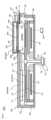
本態様に係る基板処理装置の構成について、主に図1、図2、図3を用いて説明する。図1は本態様に係る基板処理装置200を上方から見た図である。横断面概略図である。図2は本態様に係る基板処理装置200の縦断面概略図であり、図1に示すチャンバのα-α’線断面図である。なお、α-α’線は、αからチャンバ302の中心を通ってα’に向かう線である。図3は基板支持機構を説明する説明図である。(First aspect)
A first aspect will be described with reference to the drawings.
The configuration of the substrate processing apparatus according to this aspect will be described mainly with reference to FIGS. 1, 2, and 3. FIG. FIG. 1 is a top view of a
基板処理装置200の具体的構成を説明する。基板処理装置200は、後述するコントローラ400により制御される。 A specific configuration of the
図1および図2に示されているように、基板処理装置200は、主に円筒状の気密容器であるチャンバ302で構成される。チャンバ302内には、基板100を処理する処理室301が構成されている。チャンバ302にはゲートバルブ305が接続されており、ゲートバルブ305を介して基板100が搬入出される。 As shown in FIGS. 1 and 2, the
処理室301は、処理ガスを供給する処理領域306とパージガスを供給するパージ領域307を有する。ここでは処理領域306とパージ領域307は、円周状に交互に配される。例えば、第1処理領域306a、第1パージ領域307a、第2処理領域306bおよび第2パージ領域307bの順に配される。後述するように、第1処理領域306a内には第1ガスが供給され、第2処理領域306b内には第2ガスが供給され、また第1パージ領域307aおよび第2パージ領域307bには不活性ガスが供給される。これにより、それぞれの領域内に供給されるガスに応じて、基板100に対して所定の処理が施される。 The
パージ領域307は、第1処理領域306aと第2処理領域306bとを空間的に切り分ける領域である。パージ領域307の天井308は処理領域306の天井309よりも低くなるよう構成されている。第1パージ領域307aには天井308aが設けられ、第2パージ領域307bには天井308bが設けられる。各天井を低くすることで、パージ領域307の空間の圧力を高くする。この空間にパージガスを供給することで、隣り合う処理領域306を区画している。なお、パージガスは基板100上の余分なガスを除去する役割も有する。 The
チャンバ302の中央には、チャンバ302の中心に回転軸を有し、回転自在に構成される基板載置プレート317が設けられている。基板載置プレート317は、熱を透過する性質を有し、例えば石英で構成され、後述するヒータ380から放射される熱を透過させる。透過された熱は基板100を加熱する。
At the center of the
基板載置プレート317は、チャンバ302内に、複数枚(例えば5枚)の基板100を同一面上に、且つ回転方向に沿って同一円周状に配置可能なよう構成される。 The
基板載置プレート317の表面は、基板載置面311と非基板載置面325とで構成される。基板載置面311には基板100が載置される。基板載置面317は、基板載置プレート317の中心から同心円状の位置に互いに等間隔(例えば72°の間隔)で配置されている。なお、図1においては、説明の便宜上図示を省略している。 The surface of the
基板載置面311は、凹部312の底面に設けられる。それぞれの凹部312は、例えば基板載置プレート317の上面から見て円形状であり、側面から見て凹形状である。凹部312の直径は基板100の直径よりもわずかに大きくなるように構成することが好ましい。凹部312内に基板100を載置することで、基板100を基板載置面311に載置できる。 The
基板載置プレート317の表面のうち、基板載置面311面以外の面を、非基板載置面325と呼ぶ。非基板載置面325は基板100が載置されない面であり、例えば複数の凹部312の間の面や、凹部312から見てチャンバ302の中心側の面、凹部312から見てチャンバ302の外周側の領域を指す。 A surface of the
各凹部312には、ピン320が貫通する貫通孔317aが複数設けられている。基板載置プレート317下方であってゲートバルブ305と向かい合う箇所には、図3に記載の基板保持機構316が設けられている。基板保持機構316は、基板100の搬入・搬出時に、基板100を突き上げて、基板100の裏面を支持するピン320を複数有する。ピン320は延伸可能な構成であって、例えば基板保持機構316の本体に収納可能である。基板100を移載する際には、ピン320が延伸され基板100を保持する。その後、ピン320の先端が下方に移動することで、基板100は凹部312に載置される。基板保持機構316は、基板載置時にピン320を孔317aに挿入可能な構成であればよい。 Each
基板載置プレート317はコア部321に固定される。コア部321は基板載置プレート317の中心に設けられ、基板載置プレート317を固定する役割を有する。コア部321の下方にはシャフト322が配される。シャフト322はコア部321を支持する。 The
シャフト322の下方は、容器302の底部に設けられた孔323を貫通し、チャンバ302外で気密可能なベローズ304で覆われている。また、シャフト322の下端には、回転部319が設けられる。なお、シャフト322を昇降させる機能も有する場合は、昇降回転部と呼んでもよい。回転部319はコントローラ400の指示によって基板載置プレート317を回転可能に構成される。 The lower part of the
基板載置プレート317の下方には、加熱部としてのヒータ380を内包するヒータユニット381が配される。ヒータ380は、基板載置プレート317に載置した各基板100を加熱する。ヒータ380は、チャンバ302の形状に沿って円周状に配される A
ヒータ380には、ヒータ制御部387が接続される。ヒータ380はコントローラ400に電気的に接続され、コントローラ400の指示によってヒータ380への電力供給を制御し、温度制御を行う。 A
基板載置プレート317の外周には排気構造386が配される。排気構造386は、排気溝388と排気バッファ空間389とを有する。排気溝388、排気バッファ空間389は、チャンバ302の形状に沿って円周状に構成される。 An
排気構造386の底には、排気孔392が設けられる。排気孔392は処理容器304内に供給されるガスを排気する。各ガスは排気溝388、排気バッファ空間389を介して排気孔392から排気される。 A
続いてプラズマ生成部350を説明する。プラズマ生成部350は、処理領域306bの上方領域のうち、ゲートバルブ305と向かい合う箇所に設けられる。 Next, the
プラズマ生成部350を構成する容器351は、天井309上に設けられる。容器351と基板載置プレート317の間には、誘電体板352が設けられる。誘電体板352は、チャンバ302の上壁に孔を設け、その孔を塞ぐよう構成される。誘電体板352は、上壁の一部であるフランジ状の支持部309aによって支持される。支持部302は円周状に構成される。 A
誘電体板352の上方にはスロット板356が設けられる。スロット板356には、後述する複数の放射孔339が設けられる。放射孔339は、後述する領域ごとに開孔面積の和が異なるよう構成される。各領域については後述する。 A
スロット板356の上面と容器351内の内壁との間には、空間355が設けられる。容器351には、導波管358が接続される。導波管358にはマイクロ波供給部357が接続され、マイクロ波供給部357から発生されたマイクロ波は導波管358を介して空間355に供給される。 A
チャンバ302には、誘電体板352の下方にガスを供給するよう、ノズル346が設けられる。クリーニングガスがノズル346から供給される。ノズル346の先端には、フランジ309aの形状に沿って設けられた円周状の供給孔346aが設けられる。
ノズル346aを通過したクリーニングガスは、供給孔346aから誘電体板352下方に向かって供給される。 The cleaning gas that has passed through the
続いて、プラズマ生成部350がゲートバルブ205と隣接する位置に配される理由を説明する。後述するように、ゲートバルブ305を介して基板100が搬入される。その際、リフトピン320が昇降されるため、ゲートバルブ205に隣接する領域は、他の領域よりも天井を高くする必要がある。 Next, the reason why the
ところで、プラズマ生成部350はクリーニングガスのプラズマを生成するが、後述するように、基板載置面311をエッチングしない程度のエネルギーが必要である。そこで、本態様においては、天井の高いゲートバルブに隣接した領域にプラズマ生成部を設けることで、誘電体板352と基板載置面311との距離を離間させ、プラズマによって基板載置面311をエッチングしない程度に失活させる。 By the way, the
続いて、図4を用いてスロット板356について説明する。図4は基板載置プレート317とスロット板356との関係を説明する説明図である。線317bは、後述する領域356cと領域356mとの間の境界線であり、それを円周状に延長したものである。線317cは、後述する領域356eと領域356mとの間の境界線であり、それを円周状に延長したものである。 Next, the
318は基板載置プレート317上の領域を説明するものである。非基板載置面325のうち、線317aから処理容器302の中心側の領域をセンター領域318cと呼び、線317cから処理容器302の外周側の領域をエッジ領域318eと呼ぶ。また、線317bと線317cとの間の領域をミドル領域318mと呼ぶ。
基板載置面311を基準として上記領域を考えると、次のように表現される。センター領域318cは基板載置面311から見て中心側の領域であり、エッジ領域318eは基板載置面311から基板載置プレートのエッジまでを含む領域である。また、ミドル領域は、センター領域318はセンター領域318cよりも外周側であって、エッジ領域318eよりも中心側といえる。 Considering the above regions with reference to the
スロット板356は、チャンバ302の中心側から外周側にかけて、例えば3つの領域を有する。各領域は、図4に記載のように、チャンバ302の中心から領域356c、領域356m、領域356eが配される。領域356mの径方向の長さは、基板載置面311の直径と同等程度とする。 The
領域356cは、領域356mから見て、チャンバ302の中心側に配される。すなわち、領域356cは、水平方向において、基板載置面311の上方よりも中心側であり、領域318c上の一部に配される。
領域356eは、領域356mから見て、チャンバ302の外周側に配される。すなわち、領域356eは、水平方向において、基板載置面311の上方よりも外周側であり、領域318e上の一部に配される。 The
各領域336には、複数の放射孔339が配される。各領域における放射孔339の単位面積当たりの開孔面積は、領域356m<領域356c、領域356m<領域356eとなるよう構成される。すなわち、放射孔339の単位面積当たりの開孔面積は、センター領域356cが前記ミドル領域よりも広くなるよう、またはエッジ領域356eがミドル領域よりも広くなるよう構成される。 Each
マイクロ波供給部357から発生されたマイクロ波は導波管358、空間355、放射孔339を介して誘電体板352に供給され、更に誘電体板352下方に供給される。 The microwaves generated from the
マイクロ波供給と並行して、ノズル346から誘電体板352下方にクリーニングガスが供給される。クリーニングガスはマイクロ波によって活性化され、プラズマ状態とされる。 A cleaning gas is supplied from the
クリーニングガスのプラズマは、照射されるマイクロ波の量に比例することから、各領域においては、放射孔339の開孔面積に対応する。そのため、プラズマの量は領域356m<領域356c、領域356m<領域356eとなる。 Since the plasma of the cleaning gas is proportional to the amount of irradiated microwaves, each area corresponds to the opening area of the
続いて図5を用いてガス供給部を説明する。
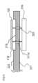
チャンバ302にはノズル341、ノズル342、ノズル344、ノズル345、ノズル346が設けられる。図1のAは図5(a)のAと接続される。すなわち、ノズル341は供給管241に接続される。図1のBは図5(b)のBと接続される。すなわち、ノズル342は供給管251に接続される。図1のCは図5(c)のCと接続される。すなわち、ノズル344、ノズル345はそれぞれ供給管261に接続される。図2のDは図5(d)のDと接続される。すなわち、ノズル346は供給管271に接続される。Next, the gas supply section will be described with reference to FIG.
図5(a)はガス供給部の一部である第1ガス供給部240である。図5(a)を用いてその詳細を説明する。第1ガス供給管241からは第1ガスが主に供給される。 FIG. 5(a) shows the first
第1ガス供給管241には、上流方向から順に、第1ガス供給源242、流量制御器(流量制御部)であるMFC243、及び開閉弁であるバルブ244が設けられている。 The first
第1ガス供給管241から第1元素を含有するガス(以下、「第1ガス」)が、MFC243、バルブ244、第1ガス供給管241を介してノズル341に供給される。 A gas containing the first element (hereinafter referred to as “first gas”) is supplied from the first
第1ガスは、原料ガス、すなわち、処理ガスの一つである。ここで、第1元素は、例えばシリコン(Si)である。すなわち、第1ガスは、Siガス(Si含有ガスとも呼ぶ)であり、Siを主成分としたガスである。具体的には、ジクロロシラン(DCS、SiH2Cl2)ガスが用いられる。The first gas is one of the raw material gases, that is, the processing gases. Here, the first element is silicon (Si), for example. That is, the first gas is Si gas (also referred to as Si-containing gas), and is a gas containing Si as a main component. Specifically, dichlorosilane (DCS, SiH2 Cl2 ) gas is used.
主に、第1ガス供給管241、MFC243、バルブ244、ガス供給構造410により第1ガス供給部240が構成される。更には、第1ガス供給源242を第1ガス供給部240に含めて考えてもよい。 The first
続いて図5(b)を用いて、ガス供給部の一部である第2ガス供給部250を説明する。
第2ガス供給管251には、上流方向から順に、第2ガス供給源252、流量制御器であるMFC253、バルブ254が設けられる。Next, the second
The second
そして、第2ガス供給管251から、第1ガスと反応する反応ガスがシャワーヘッド230内に供給される。反応ガスは第2ガスとも呼ぶ。第2ガスは処理ガスの一つであり、例えば窒素を主成分とした窒素含有ガスである。窒素含有ガスとしては、例えばアンモニア(NH3)ガスが用いられる。A reactive gas that reacts with the first gas is supplied into the shower head 230 from the second
主に、第2ガス供給管251、MFC253、バルブ254、ノズル342で第2ガス供給部250が構成される。なお、第2ガス供給部250は、反応ガスを供給する構成であるので、反応ガス供給部とも呼ぶ。更には、第2ガス供給源252を第2ガス供給部250に含めてもよい。 The second
続いて図5(c)を用いて、ガス供給部の一部であるパージガス供給部260を説明する。
パージガス供給管261には、上流方向から順に、パージガス供給源262、流量制御器(流量制御部)であるMFC263、バルブ264が設けられる。Next, the purge
The purge
そして、パージガス供給管261からは、パージガスがシャワーヘッド230内に供給される。パージガスは、第1ガスや第2ガスと反応しないガスであり、処理室301中の雰囲気をパージするパージガスの一つであり、例えば窒素(N2)ガスである。A purge gas is supplied into the shower head 230 from the purge
主に、パージガス供給管261、MFC263、バルブ264、ノズル344、ノズル345でパージガス供給部260が構成される。パージガス供給源262をパージガス供給部260に含めてもよい。 The purge
第一ガス供給部240、第二ガス供給部250をまとめて処理ガス供給部と呼ぶ。処理ガス供給部には、パージガス供給部260を含めてもよい。 The first
続いて図5(d)を用いて、ガス供給部の一部である第三ガス供給部270を説明する。第三ガス供給管271には、上流方向から順に、第三ガス供給源272、流量制御器であるMFC273、バルブ274が設けられる。 Next, the third
そして、第三ガス供給管271から、基板載置プレート217上に形成された膜を除去するためのクリーニングガスを供給する。クリーニングガスとしては、例えば三フッ化ガス(NF3)またはフッ素ガス(F2)を用いる。A cleaning gas for removing the film formed on the substrate mounting plate 217 is supplied from the third
主に、第三ガス供給管271、MFC273、バルブ274、ノズル346で第三ガス供給部270が構成される。なお、第三ガス供給部270は、クリーニングガスを供給する構成であるので、クリーニングガス供給部とも呼ぶ。更には、第三ガス供給源272を第三ガス供給部270に含めてもよい。 The third
次に排気部を説明する。
チャンバ302の下方には排気孔392が設けられる。排気口392は処理領域306毎に設けられる。第1処理領域306aに対応して排気孔392aが設けられ、第2処理領域306bに対応して排気孔392bが設けられる。Next, the exhaust section will be described.
An
排気孔392aと連通するよう、排気部334の一部である排気管334aが設けられる。排気管334aには、開閉弁としてのバルブ334d、圧力調整器(圧力調整部)としてのAPC(Auto Pressure Controller)バルブ334cを介して、真空排気装置としての真空ポンプ334bが接続されており、処理室301内の圧力が所定の圧力(真空度)となるよう真空排気し得るように構成されている。 An
排気孔392bも同様に、排気口392aと連通するよう、排気部334が接続される。排気管334a、バルブ334d、APCバルブ334cをまとめて排気部334と呼ぶ。なお、真空ポンプ334bを第1の排気部334に含めてもよい。 Similarly, the
続いて図6を用いてコントローラ400を説明する。
基板処理装置200は、マイクロ波供給部、昇降回転部、バルブ、MFC等、各部の動作を制御するコントローラ400を有している。コントローラ400は、演算部(CPU)401、一時記憶部402、記憶部403、送受信部404を少なくとも有する。コントローラ400は、送受信部404を介して基板処理装置200の各構成に接続され、上位コントローラや使用者の指示に応じて記憶部403からプログラムやレシピを呼び出し、その内容に応じて各構成の動作を制御する。なお、コントローラ400は、専用のコンピュータとして構成してもよいし、汎用のコンピュータとして構成してもよい。例えば、上述のプログラムを格納した外部記憶装置(例えば、磁気テープ、フレキシブルディスクやハードディスク等の磁気ディスク、CDやDVD等の光ディスク、MO等の光磁気ディスク、USBメモリ(USB Flash Drive)やメモリカード等の半導体メモリ)412を用意し、外部記憶装置412を用いて汎用のコンピュータにプログラムをインストールすることにより、本態様に係るコントローラ400を構成できる。また、コンピュータにプログラムを供給するための手段は、外部記憶装置412を介して供給する場合に限らない。例えば、インターネットや専用回線等の通信手段を用いても良いし、上位装置420から送受信部411を介して情報を受信し、外部記憶装置412を介さずにプログラムを供給するようにしてもよい。また、キーボードやタッチパネル等の入出力装置413を用いて、コントローラ400に指示をしても良い。Next, the
The
なお、記憶部402や外部記憶装置412は、コンピュータ読み取り可能な記録媒体として構成される。以下、これらを総称して、単に記録媒体ともいう。なお、本明細書において記録媒体という言葉を用いた場合は、記憶部402単体のみを含む場合、外部記憶装置412単体のみを含む場合、または、その両方を含む場合がある。 Note that the
(基板処理工程)
次に、図7を用い、基板処理工程について説明する。図7は、本態様に係る基板処理工程を示すフロー図である。以下の説明において、基板処理装置200の構成各部の動作は、コントローラ400により制御される。(Substrate processing step)
Next, the substrate processing process will be described with reference to FIG. FIG. 7 is a flowchart showing a substrate processing process according to this aspect. In the following description, the
ここでは、第1ガスとしてシリコン含有ガスを用い、第2ガスとしてアンモニアガスを用い、基板100に薄膜として窒化シリコン(SiN)膜を形成する例について説明する。 Here, an example in which a silicon-containing gas is used as the first gas and ammonia gas is used as the second gas to form a silicon nitride (SiN) film as a thin film on the
基板搬入・載置工程を説明する。図7においては図示を省略する。基板載置プレート317を回転させ、凹部312をゲートバルブ305と隣接する位置に移動さする。次に、リフトピン320を上昇させ、基板載置プレート317の貫通孔317aに貫通させる。続いて、ゲートバルブ305を開いてチャンバ302と真空搬送室(図示せず)と連通させる。そして、この移載室からウエハ移載機(図示せず)を用いて基板100をリフトピン320上に移載し、その後リフトピン320を下降させる。これにより、基板100は基板載置面311上に支持される。 A substrate carrying-in/placing step will be described. Illustration is omitted in FIG. The
基板100が基板載置面311上に載置されたら、基板100が載置されていない基板載置面311がゲートバルブ305と向かい合うよう、基板載置プレート317を回転させる。その後、同様に基板載置面311に基板を載置する。すべての基板載置面311に基板100が載置されるまで繰り返す。 After the
基板100を基板載置プレート317に載置する際は、予めヒータ380に電力を供給し、基板100の表面が所定の温度となるよう制御する。基板100の温度は、例えば400℃以上であって500℃以下である。ヒータ380から放射された熱は、基板載置プレート317を介して基板100の裏面に照射される。ヒータ380は、少なくとも基板搬入・載置工程から後述する基板搬出工程が終了するまでの間は、常に通電させた状態とする。 When mounting the
基板載置プレート回転開始工程S110を説明する。基板100が各凹部312に載置されたら、回転部324は基板載置プレート317をR方向に回転させる。基板載置プレート317を回転させることにより、基板100は、第1処理領域306a、第1パージ領域307a、第2処理領域306b、第2パージ領域307bの順に移動する。 The substrate mounting plate rotation start step S110 will be described. After the
ガス供給開始工程S120を説明する。基板100を加熱して所望とする温度に達し、基板載置プレート317が所望とする回転速度に到達したら、バルブ244を開けて第1処理領域306a内にシリコン含有ガスの供給を開始する。それと併行して、バルブ254を開けて第2処理領域306b内にNH3ガスを供給する。The gas supply start step S120 will be described. When the
このとき、シリコン含有ガスの流量が所定の流量となるように、MFC243を調整する。なお、シリコン含有ガスの供給流量は、例えば50sccm以上500sccm以下である。 At this time, the
また、NH3ガスの流量が所定の流量となるように、MFC253を調整する。なお、NH3ガスの供給流量は、例えば100sccm以上5000sccm以下である。Also, the
なお、基板搬入・載置工程後、継続して、第1の排気部33により処理室301内が排気されるとともに、不活性ガス供給部260から第1パージ領域307a内および第2パージ領域307b内にパージガスとしてのN2ガスが供給されている。After the substrate carrying-in/placing process, the inside of the
成膜工程S130を説明する。成膜工程S130では、各基板100は、第1処理領域306aにてシリコン含有層が形成され、更に回転後の第2処理領域306bにて、シリコン含有層とNH3ガスとが反応し、基板100上にシリコン含有膜を形成する。所望の膜厚となるよう、基板載置プレート317を所定回数回転させる。このとき、非基板載置面325にもガスが供給されるため、非基板載置面325上にも膜が形成される。The film forming step S130 will be described. In the film formation step S130, each
ガス供給停止工程S140を説明する。所定回数回転させた後、バルブ244,バルブ254を閉じ、第1処理領域306aへのシリコン含有ガスの供給、第2処理領域306bへのNH3ガスの供給を停止する。The gas supply stop step S140 will be described. After rotating a predetermined number of times, the
基板載置プレート回転停止工程S150を説明する。ガス供給停止工程S140の後、基板載置プレート317の回転を停止する。 The substrate mounting plate rotation stop step S150 will be described. After the gas supply stop step S140, the rotation of the
基板搬出工程を説明する。図7では図示を省略している。
ゲートバルブ305と隣接する位置に搬出したい基板100を移動するよう基板載置プレートを回転させる。その後、基板搬入時と逆の方法で基板を搬出する。これらの動作を繰り返し、すべての基板100を搬出する。A substrate unloading process will be described. Illustration is omitted in FIG.
The substrate mounting plate is rotated so as to move the
続いてクリーニング工程を説明する。クリーニング工程は、基板処理工程のうちの一工程である。クリーニング工程は、基板100が基板処理装置200に存在しない状態で行われる。故に、基板載置面311上には基板100が載置されていない。 Next, the cleaning process will be explained. The cleaning process is one of the substrate processing processes. The cleaning process is performed while the
成膜工程S130にて非基板載置面325表面に形成された膜が剥がれてパーティクルになると、基板100に悪影響を及ぼす場合がある。例えば、基板100に剥がれた膜が付着した場合、基板100に形成されたデバイスの抵抗値が変化する等、品質が低下する。 If the film formed on the surface of the
そこで、本工程では非基板載置面325表面をクリーニングし、非基板載置面325表面上に形成された膜の膜剥がれを抑制することが考えられる。クリーニング処理では、後述するようにプラズマ状態のクリーニングガスによってクリーニングされる。 Therefore, in this step, it is conceivable to clean the surface of the
ここで比較例を説明する。比較例は、クリーニング処理する際、非基板載置面325と基板載置面311をクリーニングする例である。前述のようにクリーニング処理は基板100が無い状態、すなわち基板載置面311がむき出しになった状態で行われる。したがって、プラズマ状態のクリーニングガスは基板載置面311に照射されてしまう。 A comparative example will now be described. A comparative example is an example in which the
プラズマ状態のクリーニングガスは基板載置面311をエッチングしてしまうが、その場合ヒータ380から放射された熱の屈折率が変化してしまうことが考えられる。屈折率が変化すると、基板100の裏面全体に放射される熱が、エッチング前に比べて変化してしまう。例えば、屈折率が異なる箇所は、エッチング前に比べて熱を透過しにくくなったり、反射してしまったりする等の異常が発生し、そうなると基板100を均一に加熱器できなくなってしまう。 The cleaning gas in the plasma state etches the
そこで本態様では、基板載置面311のエッチングを抑制しつつ、非基板載置面をクリーニングする。以下に具体的な方法を説明する。 Therefore, in this aspect, the non-substrate mounting surface is cleaned while suppressing the etching of the
基板100が基板処理室200から搬出されたら、ゲートバルブ305を閉じる。その後、マイクロ波供給部357がマイクロ波を発生させる。それと並行して、ノズル346から誘電体板352下方にクリーニングガスを供給する。供給されたクリーニングガスは誘電体板352下方に生成される。クリーニングガスはプラズマ状態になる。 After the
領域356mの開孔面積<領域356cの開孔面積であることから、それぞれの領域のプラズマ密度に関しては領域356cが領域356mよりも高くなるよう生成される。また、領域356mの開孔面積<領域356eの開孔面積であることから、それぞれの領域のプラズマ密度に関しては領域356eが領域356mよりも高くなるよう生成される。 Since the opening area of the
続いて、このような密度の関係でプラズマを生成する理由を説明する。前述のように、成膜工程S130の間、基板100は基板載置面311上に載置されている。そのため、基板載置面311はガスに晒されにくく、したがって膜は形成されにくい。 Next, the reason why plasma is generated in such a density relationship will be described. As described above, the
一方、非基板載置面325はガスに晒されるため、膜が形成される。すなわち、形成される膜は、基板載置面311よりも非基板載置面325のほうが厚くなる。 On the other hand, since the
このような状態で、領域356c、356m、356eにおいて同密度のプラズマを生成した場合、次の問題がある。一つは、プラズマが基板載置面311をエッチングしてしまう点である。例えば、非基板載置面325の内、処理チャンバ202の中心側の膜を早期に除去するために強いプラズマを用いた場合、領域356mの下方を通過する基板載置面311も強いプラズマに晒される。そのため、強いプラズマによって基板載置面311がエッチングされる恐れがある。エッチングされた場合、基板載置面311における熱の透過率が変化し、均一に加熱できない。 If plasma with the same density is generated in the
もう一つは、基板載置面355がエッチングしない程度の強さのプラズマとした場合、非基板載置面325の中心側と外周側の膜を除去するのに時間がかかり、長時間のダウンタイムが要求される点である。 Another problem is that if the plasma is strong enough not to etch the
このような問題があることから、領域318m上では、他の領域に比べてプラズマ密度を低くする。それを実現すべく、領域356mの開孔面積<領域356cの開孔面積とした。また、領域356mの開孔面積<領域356eの開孔面積とした。 Due to such problems, the plasma density is made lower on the
これにより、基板載置面311をエッチングすることなく、短時間で非基板載置面325の表面をクリーニングできる。 As a result, the surface of the
プラズマが生成されたら、基板載置プレート317の回転を開始する。基板載置面311が領域356m下方を通過する間は回転を継続する。回転する間、領域356c、領域356e下方の非基板載置面325上の膜がクリーニングされる。基板載置面311上にクリーニングガスのプラズマが晒されるものの、基板載置プレート317が回転しているため、基板載置面311上にプラズマが滞留することがない。 After the plasma is generated, the rotation of the
また、基板載置面311が領域356m下方に無い場合、すなわち基板載置面311の間の非基板載置面325が領域356m下方に存在する場合は、回転を停止する。回転を停止することで、基板載置面311の間の非基板載置面325上をクリーニングする。ここでは、クリーニングガスが非基板載置面325上に滞留するため、非基板載置面325上の膜がクリーニングされる。 Further, when the
以上のように、基板載置プレート317の回転と停止を繰り返すことで、基板載置面311をエッチングすることなく、非基板載置面325全体をクリーニングできる。したがって、基板100を均一に加熱できる。 By repeating the rotation and stopping of the
(第2の態様)
続いて、図8から図10を用いて第2の態様を説明する。図8は図2に相当する図であり、基板処理装置200を側方から見た図である。図9は、基板載置プレート317とスロット板361との関係を説明する図である。図10は基板載置プレート317、スロット板361、移動板362との関係を説明する図である。(Second aspect)
Next, a second aspect will be described with reference to FIGS. 8 to 10. FIG. FIG. 8 is a diagram corresponding to FIG. 2, and is a diagram of the
第2の態様は、第1の態様と比べて誘電体板360、スロット板361の形態が異なると共に、スロット板361上に、開孔391の単位面積当たりの開孔面積を領域ごとに調整可能な移動板362が設けられる点が主に異なる。更に、クリーニング工程における具体的な処理が異なる。他は同様の構成である。以下に、相違点を中心に説明する。 The second mode differs from the first mode in the forms of the
誘電体板360上にはスロット板361が設けられる。図9に記載のように、スロット板361は長方形であり、処理容器302の中心から外周にかけて配される。スロット板361には放射孔339が均等に設けられている。誘電体360はスロット板361と同様に長方形である。上方から見て誘電体360とスロット板361とは重なるよう構成される。 A
スロット板361上には移動板362が配される。移動板362は長方形であり、処理容器の中心から外周にかけて稼働可能に構成されている。容器351の隣には、移動板362が収容される収容容器としての容器363が設けられる。容器363には空間364が設けられ、移動板362は図示しない移動機構により容器363と容器351との間、具体的にはスロット板361上の空間との間を往復移動するよう構成される。 A moving
図10に記載のように、移動板362は処理容器302の中心側である第一部位362aと、それよりも外周側にある第二部位362bとを有する。第二部位362bの処理容器302の径方向の長さは、基板載置面311の径と同等の長さである。第一部位362aのうち、処理容器302の径方向の長さは、領域318cをカバーできる長さである。 As shown in FIG. 10, the moving
第一部位362aは、中央に孔が形成された枠であり、スロット板361と移動板362とが重なった際には、空間355から見て放射孔339を露出するよう構成される。第二部位362bは例えば孔の無い板であり、スロット板361と移動板362とが重なった際には、空間355から見て放射孔339を塞ぐよう構成される。 The
第一部位362aは放射孔339を露出させることから、露出部とも呼ぶ。また、孔を有していることから、有孔部とも呼ぶ。第二部位362bは放射孔339を塞ぐことから、塞部とも呼ぶ。また、第二部位は孔を有しないため、無孔部とも呼ぶ。 Since the
続いて、本態様におけるクリーニング工程を説明する。第一の態様と同様、クリーニング工程を行う際には、クリーニングガスのプラズマを生成する。それと並行して、基板載置プレート317の回転を開始する。 Next, the cleaning process in this embodiment will be described. As in the first mode, plasma of the cleaning gas is generated when performing the cleaning process. In parallel with this, the rotation of the
その際、基板載置面311がプラズマ生成部350の下方を通過する際は、移動板362はスロット板361上に配される。具体的には、基板載置面311上の放射孔339を塞ぐよう第二部位362bが移動する。このとき、第一部位362aも移動するが、第一部位362aには孔が設けられているため、領域318c上の放射孔339は塞がれることがない。このように移動板362を移動することで、図10のように、領域318mの放射孔339がふさがれると共に、領域318c、領域318eの放射孔339が解放される。したがって、基板載置面311上にはプラズマが生成されず、非基板載置面325上の領域318c、領域318eではプラズマが生成される。このようにして領域318c、領域318eをクリーニングする。 At that time, when the
また、非基板載置面325のうち、隣接する基板載置面311の間の領域をクリーニングする際は、隣接する基板載置面311の間の領域が、プラズマ生成部350の下方を通過する間、移動板362を容器363に退避させる。退避させることで、領域318c、領域318m、領域318eそれぞれで放射孔が解放される。したがって、非基板載置面325のうち、領域318c、領域318eと、隣接する基板載置面311の間の領域にプラズマを供給することができる。このようにして、中央領域と外周領域と基板載置面の間の領域とをクリーニングする。 Further, when cleaning the region between the adjacent
以上のように、基板載置面311の移動に合わせて移動板362を移動させることで、基板載置面311をエッチングすることなく、非基板載置面325全体をクリーニングできる。したがって、基板100を均一に加熱できる。 As described above, by moving the moving
本態様においては、移動板362を処理室301の中心側から外周側にかけて稼働するようにしたが、それに限るものではなく、基板載置面311上の放射孔を塞ぐ構造であればよい。例えば、移動板362を処理室301の外周側から中心側にかけて稼働させてもよい。その場合、第一部位362aは処理室301の外周側に設けられる。更には、容器361が容器351の外周側に設けられる。 In this embodiment, the moving
(第3の態様)
続いて、図11と図12とを用いて第3の態様を説明する。図11は図2に相当する図であり、基板処理装置200を側方から見た図である。図12は、基板載置プレート317とスロット板361との関係を説明する図である。(Third aspect)
Next, a third aspect will be described with reference to FIGS. 11 and 12. FIG. FIG. 11 is a diagram corresponding to FIG. 2, and is a diagram of the
第3の態様は、第1の態様と比べてスロット板371の形状が異なる。以下に、相違点を中心に説明する。 The third aspect differs from the first aspect in the shape of the
スロット板371は、チャンバ302の中心側から外周側にかけて設けられる。領域325bでは、基板載置面311と同様の大きさの第一領域371aが形成される。スロット板371のうち、領域371b以外の第二領域371bには放射孔339が設けられている。領域371aには放射孔339は設けられていない。 The
第一領域371aは孔を有していないので、無孔部とも呼ぶ。第二領域371bは孔を有していることから、有孔部とも呼ぶ。 Since the
続いて、本態様におけるクリーニング工程を説明する。プラズマが生成されたら、基板載置プレート317の回転を開始する。基板載置面311が領域371aの下方に移動したら、回転を停止する。 Next, the cleaning process in this embodiment will be described. After the plasma is generated, the rotation of the
回転を停止した状態では、基板載置面311が領域371aの下方に配され、非基板載置面325の一部が領域371bの下方に配される。基板載置面311にプラズマが晒されず、その外側の非基板載置面325にプラズマが晒される。したがって、基板載置面311をエッチングせずに、非基板載置面325のクリーニングが可能となる。 When the rotation is stopped, the
所定時間経過したら基板載置プレート317を回転させる。回転は、隣接する基板載置面311が領域371bの下方に配されるまで継続される。その間、基板載置面311間の非基板載置面325はプラズマ状態のクリーニングガスに晒され、クリーニングされる。なお、ここでは回転することを記載したが、隣接する基板載置面311間の領域がプラズマ生成部350の下方に配された状態であればよく、例えば停止した状態であってもよい。 After a predetermined time has passed, the
以上のように、基板載置面311の移動に合わせてプラズマ処理することで、基板載置面311をエッチングすることなく、非基板載置面325全体をクリーニングできる。 As described above, the
(他の態様)
以上、本開示の第1の態様から第3の態様を具体的に説明したが、本開示が上述の各態様に限定されることはなく、その要旨を逸脱しない範囲で種々変更することが可能である。(Other aspects)
Although the first to third aspects of the present disclosure have been specifically described above, the present disclosure is not limited to the above-described aspects, and various changes can be made without departing from the gist thereof. is.
100 基板
200 基板処理装置
240 第一ガス供給部
250 第二ガス供給部
270 第三ガス供給部
301 処理室
302 チャンバ
317 基板載置プレート
324 回転部
334 ガス排気部
350 プラズマ生成部
380 ヒータ
Claims (11)
Translated fromJapanese非基板載置面と複数の基板載置面とを備える基板載置プレートと、
前記基板載置プレートを回転させる回転部と、
前記基板載置面上のプラズマ密度よりも前記非基板載置面上のプラズマ密度が高くなるよう構成されたプラズマ生成部と、
前記処理室に処理ガスを供給する処理ガス供給部と、
前記処理室に、前記プラズマ生成部によってプラズマ状態とされるクリーニングガスを供給するクリーニングガス供給部と、
前記基板載置プレートの下方に配されたヒータと
を有する基板処理装置。a processing chamber for processing substrates;
a substrate mounting plate comprising a non-substrate mounting surface and a plurality of substrate mounting surfaces;
a rotating part that rotates the substrate mounting plate;
a plasma generator configured such that the plasma density on the non-substrate mounting surface is higher than the plasma density on the substrate mounting surface;
a processing gas supply unit that supplies a processing gas to the processing chamber;
a cleaning gas supply unit that supplies a cleaning gas that is turned into a plasma state by the plasma generation unit into the processing chamber;
A substrate processing apparatus comprising: a heater arranged below the substrate mounting plate.
前記プラズマ生成部は、前記ゲートバルブに隣接するよう構成される請求項1から請求項3のうち、いずれか一項に記載の基板処理装置。Furthermore, the processing chamber is provided with a gate valve,
The substrate processing apparatus according to any one of claims 1 to 3, wherein the plasma generator is configured to be adjacent to the gate valve.
前記プラズマ生成部は、前記センター領域のプラズマ密度が前記ミドル領域のプラズマ密度よりも高くなるよう、または前記エッジ領域のプラズマ密度が前記ミドル領域のプラズマ密度よりも高くなるよう構成される請求項1から請求項4のうち、いずれか一項に記載の基板処理装置。The processing chamber includes a center region that is a region closer to the center than the substrate mounting surface, a middle region that is outer peripheral than the center region and includes the substrate mounting surface, and a middle region extending from the substrate mounting surface. and an edge region including an edge of the substrate mounting plate,
2. The plasma generation unit is configured such that the plasma density in the center region is higher than the plasma density in the middle region, or the plasma density in the edge region is higher than the plasma density in the middle region. 5. The substrate processing apparatus according to any one of claims 4 to 4.
前記プラズマ生成部は、誘電体板と、前記誘電体板上に設けられ複数の放射孔を有するスロット板と、マイクロ波供給部とを有し、
前記放射孔の単位面積当たりの開孔面積は、前記センター領域が前記ミドル領域よりも広くなるよう、または前記エッジ領域が前記ミドル領域よりも広くなるよう構成される請求項1から請求項4のうち、いずれか一項に記載の基板処理装置。The processing chamber includes a center region that is a region closer to the center than the substrate mounting surface, a middle region that is outer peripheral than the center region and includes the substrate mounting surface, and a middle region extending from the substrate mounting surface. and an edge region including an edge of the substrate mounting plate,
The plasma generation unit has a dielectric plate, a slot plate provided on the dielectric plate and having a plurality of radiation holes, and a microwave supply unit,
5. A hole area per unit area of said radiation hole is configured such that said center region is wider than said middle region, or said edge region is wider than said middle region. The substrate processing apparatus according to any one of the items.
前記プラズマ生成部は、誘電体板と、前記誘電体板上に設けられ、複数の放射孔を有するスロット板と、マイクロ波供給部と、
前記プラズマ生成部に隣接した容器と、
前記容器内と前記スロット板上の間を移動可能であって、クリーニング処理時には前記センター領域もしくは前記エッジ領域上に配され、前記センター領域もしくは前記エッジ領域の前記放射孔を露出する第一部位と、前記クリーニング処理時には前記ミドル領域上に配され、前記ミドル領域上の放射孔を塞ぐ第二部位とを有する移動板とを有する請求項1から請求項4のうち、いずれか一項に記載の基板処理装置。The processing chamber includes a center region that is a region closer to the center than the substrate mounting surface, a middle region that is outer peripheral than the center region and includes the substrate mounting surface, and a middle region extending from the substrate mounting surface. and an edge region including an edge of the substrate mounting plate,
The plasma generation unit includes a dielectric plate, a slot plate provided on the dielectric plate and having a plurality of radiation holes, a microwave supply unit,
a container adjacent to the plasma generator;
a first portion movable between the inside of the container and the slot plate, disposed on the center region or the edge region during a cleaning process, and exposing the radiation holes in the center region or the edge region; and a moving plate disposed on the middle region during the cleaning process, and a second portion for closing the radiation hole on the middle region. Substrate processing equipment.
前記基板載置面の間の領域が前記プラズマ生成部下方を通過する間、前記移動板を前記容器に退避させる請求項7に記載の基板処理装置。When cleaning the region between the adjacent substrate mounting surfaces among the non-substrate mounting surfaces,
8. The substrate processing apparatus according to claim 7, wherein the moving plate is retracted to the container while the region between the substrate mounting surfaces is passing below the plasma generating section.
前記プラズマ生成部は、誘電体板と、前記誘電体板上に設けられ、複数の放射孔を有するスロット板と、マイクロ波供給部と、を有し
前記スロット板のうち、前記ミドル領域には前記基板載置面に対応した無孔部が設けられ、前記センター領域および前記エッジ領域には放射孔を有する有孔部が設けられる請求項1から請求項4のうち、いずれか一項に記載の基板処理装置。The processing chamber includes a center region that is a region closer to the center than the substrate mounting surface, a middle region that is outer peripheral than the center region and includes the substrate mounting surface, and a middle region extending from the substrate mounting surface. and an edge region including an edge of the substrate mounting plate,
The plasma generation unit includes a dielectric plate, a slot plate provided on the dielectric plate and having a plurality of radiation holes, and a microwave supply unit. 5. The device according to any one of claims 1 to 4, wherein a non-porous portion corresponding to said substrate mounting surface is provided, and a perforated portion having radiation holes is provided in said center region and said edge region. substrate processing equipment.
前記基板載置面に基板を載置する工程と、
回転部が前記基板載置プレートを回転させ、処理ガス供給部から処理ガスを供給し、ヒータが前記基板載置プレートの下方から前記基板を加熱して基板を処理する工程と、
前記基板を搬出する工程と、
前記処理室に基板が無い状態でクリーニングガスを供給すると共に、プラズマ生成部が前記基板載置面上のプラズマ密度よりも前記非基板載置面上のプラズマ密度が高くなるよう前記クリーニングガスのプラズマを生成する工程と
を有する半導体装置の製造方法。loading a substrate into a processing chamber having a substrate mounting plate with a non-substrate mounting surface and a plurality of substrate mounting surfaces;
placing a substrate on the substrate placement surface;
a rotating portion rotating the substrate mounting plate, supplying a processing gas from a processing gas supply portion, and a heater heating the substrate from below the substrate mounting plate to process the substrate;
unloading the substrate;
A cleaning gas is supplied to the processing chamber in a state where there is no substrate, and the plasma generation unit generates plasma of the cleaning gas so that the plasma density on the non-substrate mounting surface is higher than the plasma density on the substrate mounting surface. A method of manufacturing a semiconductor device, comprising:
前記基板載置面に基板を載置する手順と、
回転部が前記基板載置プレートを回転させ、処理ガス供給部から処理ガスを供給し、ヒータが前記基板載置プレートの下方から前記基板を加熱して基板を処理する手順と、
前記基板を搬出する手順と、
前記処理室に基板が無い状態でクリーニングガスを供給すると共に、プラズマ生成部が前記基板載置面上のプラズマ密度よりも前記非基板載置面上のプラズマ密度が高くなるよう前記クリーニングガスのプラズマを生成する手順と
をコンピュータによって半導体製造装置に実行させるプログラム。
loading a substrate into a processing chamber having a substrate mounting plate with a non-substrate mounting surface and a plurality of substrate mounting surfaces;
a step of placing a substrate on the substrate placement surface;
a procedure in which a rotating section rotates the substrate mounting plate, a processing gas is supplied from a processing gas supply section, and a heater heats the substrate from below the substrate mounting plate to process the substrate;
a step of unloading the substrate;
A cleaning gas is supplied to the processing chamber in a state where there is no substrate, and the plasma generation unit generates plasma of the cleaning gas so that the plasma density on the non-substrate mounting surface is higher than the plasma density on the substrate mounting surface. and a program for causing semiconductor manufacturing equipment to execute by a computer.
Priority Applications (5)
| Application Number | Priority Date | Filing Date | Title |
|---|---|---|---|
| JP2020125019AJP7242612B2 (en) | 2020-07-22 | 2020-07-22 | SUBSTRATE PROCESSING APPARATUS, SEMICONDUCTOR DEVICE MANUFACTURING METHOD AND PROGRAM |
| TW109127199ATWI782307B (en) | 2020-07-22 | 2020-08-11 | Substrate processing apparatus, manufacturing method of semiconductor device, and manufacturing program of semiconductor device |
| KR1020200120327AKR102504557B1 (en) | 2020-07-22 | 2020-09-18 | Substrate processing apparatus, method of manufacturing semiconductor device and non-transitory computer-readable recording medium |
| US17/027,311US11664205B2 (en) | 2020-07-22 | 2020-09-21 | Substrate processing apparatus |
| CN202011006528.1ACN113972149A (en) | 2020-07-22 | 2020-09-23 | Substrate processing apparatus, manufacturing method of semiconductor device, and storage medium |
Applications Claiming Priority (1)
| Application Number | Priority Date | Filing Date | Title |
|---|---|---|---|
| JP2020125019AJP7242612B2 (en) | 2020-07-22 | 2020-07-22 | SUBSTRATE PROCESSING APPARATUS, SEMICONDUCTOR DEVICE MANUFACTURING METHOD AND PROGRAM |
Publications (2)
| Publication Number | Publication Date |
|---|---|
| JP2022021458A JP2022021458A (en) | 2022-02-03 |
| JP7242612B2true JP7242612B2 (en) | 2023-03-20 |
Family
ID=79586023
Family Applications (1)
| Application Number | Title | Priority Date | Filing Date |
|---|---|---|---|
| JP2020125019AActiveJP7242612B2 (en) | 2020-07-22 | 2020-07-22 | SUBSTRATE PROCESSING APPARATUS, SEMICONDUCTOR DEVICE MANUFACTURING METHOD AND PROGRAM |
Country Status (5)
| Country | Link |
|---|---|
| US (1) | US11664205B2 (en) |
| JP (1) | JP7242612B2 (en) |
| KR (1) | KR102504557B1 (en) |
| CN (1) | CN113972149A (en) |
| TW (1) | TWI782307B (en) |
Citations (3)
| Publication number | Priority date | Publication date | Assignee | Title |
|---|---|---|---|---|
| JP2016176129A (en) | 2015-03-20 | 2016-10-06 | 株式会社日立国際電気 | Substrate processing apparatus, semiconductor device manufacturing method, program, and recording medium |
| JP2017514991A (en) | 2014-04-25 | 2017-06-08 | アプライド マテリアルズ インコーポレイテッドApplied Materials,Incorporated | Plasma corrosion resistant thin film coating for high temperature applications |
| JP2019003998A (en) | 2017-06-13 | 2019-01-10 | 東京エレクトロン株式会社 | Film forming apparatus, film forming apparatus cleaning method, and storage medium |
Family Cites Families (11)
| Publication number | Priority date | Publication date | Assignee | Title |
|---|---|---|---|---|
| JP2509813B2 (en)* | 1986-11-04 | 1996-06-26 | 日本真空技術株式会社 | Vacuum processing method and apparatus |
| JP4563729B2 (en)* | 2003-09-04 | 2010-10-13 | 東京エレクトロン株式会社 | Plasma processing equipment |
| JP2008181710A (en) | 2007-01-23 | 2008-08-07 | Canon Inc | Plasma processing apparatus and method |
| JP2011150943A (en)* | 2010-01-22 | 2011-08-04 | Tokyo Electron Ltd | Plasma processing apparatus, and substrate processing method employing the same |
| US20120164834A1 (en) | 2010-12-22 | 2012-06-28 | Kevin Jennings | Variable-Density Plasma Processing of Semiconductor Substrates |
| US9155183B2 (en)* | 2012-07-24 | 2015-10-06 | Tokyo Electron Limited | Adjustable slot antenna for control of uniformity in a surface wave plasma source |
| JP5947138B2 (en)* | 2012-07-25 | 2016-07-06 | 東京エレクトロン株式会社 | Deposition equipment |
| US9831067B2 (en)* | 2012-10-11 | 2017-11-28 | Tokyo Electron Limited | Film-forming apparatus |
| JP6051788B2 (en)* | 2012-11-05 | 2016-12-27 | 東京エレクトロン株式会社 | Plasma processing apparatus and plasma generating apparatus |
| JP6298383B2 (en) | 2014-08-19 | 2018-03-20 | 株式会社日立国際電気 | Substrate processing apparatus and semiconductor device manufacturing method |
| JP7246217B2 (en)* | 2019-03-19 | 2023-03-27 | 東京エレクトロン株式会社 | Method for cleaning deposition equipment |
- 2020
- 2020-07-22JPJP2020125019Apatent/JP7242612B2/enactiveActive
- 2020-08-11TWTW109127199Apatent/TWI782307B/enactive
- 2020-09-18KRKR1020200120327Apatent/KR102504557B1/enactiveActive
- 2020-09-21USUS17/027,311patent/US11664205B2/enactiveActive
- 2020-09-23CNCN202011006528.1Apatent/CN113972149A/enactivePending
Patent Citations (3)
| Publication number | Priority date | Publication date | Assignee | Title |
|---|---|---|---|---|
| JP2017514991A (en) | 2014-04-25 | 2017-06-08 | アプライド マテリアルズ インコーポレイテッドApplied Materials,Incorporated | Plasma corrosion resistant thin film coating for high temperature applications |
| JP2016176129A (en) | 2015-03-20 | 2016-10-06 | 株式会社日立国際電気 | Substrate processing apparatus, semiconductor device manufacturing method, program, and recording medium |
| JP2019003998A (en) | 2017-06-13 | 2019-01-10 | 東京エレクトロン株式会社 | Film forming apparatus, film forming apparatus cleaning method, and storage medium |
Also Published As
| Publication number | Publication date |
|---|---|
| KR20220012152A (en) | 2022-02-03 |
| US20220028669A1 (en) | 2022-01-27 |
| US11664205B2 (en) | 2023-05-30 |
| TWI782307B (en) | 2022-11-01 |
| KR102504557B1 (en) | 2023-02-27 |
| CN113972149A (en) | 2022-01-25 |
| JP2022021458A (en) | 2022-02-03 |
| TW202205500A (en) | 2022-02-01 |
Similar Documents
| Publication | Publication Date | Title |
|---|---|---|
| US20170232457A1 (en) | Substrate processing apparatus and precursor gas nozzle | |
| JP4237833B2 (en) | Method and apparatus for protecting a susceptor using a ceramic wafer during process chamber cleaning | |
| KR102584230B1 (en) | Tabernacle equipment and method | |
| CN106158568A (en) | Lining processor, the manufacture method of semiconductor devices and gas distribution assembly | |
| JP6995073B2 (en) | Manufacturing methods and programs for substrate processing equipment and semiconductor equipment | |
| KR102729762B1 (en) | Substrate processing apparatus, non-transitory computer-readable recording medium, substrate processing method and method of manufacturing semiconductor device | |
| JP7364547B2 (en) | Semiconductor device manufacturing method, substrate processing equipment and program | |
| JP7223047B2 (en) | SUBSTRATE PROCESSING APPARATUS, SEMICONDUCTOR DEVICE MANUFACTURING METHOD AND PROGRAM | |
| JP7242612B2 (en) | SUBSTRATE PROCESSING APPARATUS, SEMICONDUCTOR DEVICE MANUFACTURING METHOD AND PROGRAM | |
| JP6894482B2 (en) | Substrate processing equipment, semiconductor device manufacturing methods, programs and recording media | |
| US12297536B2 (en) | Substrate processing apparatus and substrate processing method | |
| CN112176322A (en) | Substrate processing apparatus, method for manufacturing semiconductor device, and program | |
| TWI802005B (en) | Substrate processing apparatus, method and program for manufacturing semiconductor device | |
| US11380540B2 (en) | Substrate processing apparatus | |
| KR102834836B1 (en) | Substrate processing apparatus, method of manufacturing semiconductor device, and recording medium | |
| JP7446189B2 (en) | Processing equipment and processing method | |
| WO2024195077A1 (en) | Substrate processing device, substrate processing method, method for producing semiconductor device, and program |
Legal Events
| Date | Code | Title | Description |
|---|---|---|---|
| A521 | Request for written amendment filed | Free format text:JAPANESE INTERMEDIATE CODE: A523 Effective date:20210324 | |
| A621 | Written request for application examination | Free format text:JAPANESE INTERMEDIATE CODE: A621 Effective date:20210324 | |
| A977 | Report on retrieval | Free format text:JAPANESE INTERMEDIATE CODE: A971007 Effective date:20220422 | |
| A131 | Notification of reasons for refusal | Free format text:JAPANESE INTERMEDIATE CODE: A131 Effective date:20220510 | |
| A521 | Request for written amendment filed | Free format text:JAPANESE INTERMEDIATE CODE: A523 Effective date:20220705 | |
| A131 | Notification of reasons for refusal | Free format text:JAPANESE INTERMEDIATE CODE: A131 Effective date:20221011 | |
| A521 | Request for written amendment filed | Free format text:JAPANESE INTERMEDIATE CODE: A523 Effective date:20221207 | |
| TRDD | Decision of grant or rejection written | ||
| A01 | Written decision to grant a patent or to grant a registration (utility model) | Free format text:JAPANESE INTERMEDIATE CODE: A01 Effective date:20230221 | |
| A61 | First payment of annual fees (during grant procedure) | Free format text:JAPANESE INTERMEDIATE CODE: A61 Effective date:20230308 | |
| R150 | Certificate of patent or registration of utility model | Ref document number:7242612 Country of ref document:JP Free format text:JAPANESE INTERMEDIATE CODE: R150 |