JP7228725B2 - Display device - Google Patents
Display deviceDownload PDFInfo
- Publication number
- JP7228725B2 JP7228725B2JP2022018869AJP2022018869AJP7228725B2JP 7228725 B2JP7228725 B2JP 7228725B2JP 2022018869 AJP2022018869 AJP 2022018869AJP 2022018869 AJP2022018869 AJP 2022018869AJP 7228725 B2JP7228725 B2JP 7228725B2
- Authority
- JP
- Japan
- Prior art keywords
- transistor
- conductive layer
- wiring
- channel formation
- plan
- Prior art date
- Legal status (The legal status is an assumption and is not a legal conclusion. Google has not performed a legal analysis and makes no representation as to the accuracy of the status listed.)
- Active
Links
Images


Classifications
- H—ELECTRICITY
- H10—SEMICONDUCTOR DEVICES; ELECTRIC SOLID-STATE DEVICES NOT OTHERWISE PROVIDED FOR
- H10D—INORGANIC ELECTRIC SEMICONDUCTOR DEVICES
- H10D86/00—Integrated devices formed in or on insulating or conducting substrates, e.g. formed in silicon-on-insulator [SOI] substrates or on stainless steel or glass substrates
- H10D86/40—Integrated devices formed in or on insulating or conducting substrates, e.g. formed in silicon-on-insulator [SOI] substrates or on stainless steel or glass substrates characterised by multiple TFTs
- G—PHYSICS
- G02—OPTICS
- G02F—OPTICAL DEVICES OR ARRANGEMENTS FOR THE CONTROL OF LIGHT BY MODIFICATION OF THE OPTICAL PROPERTIES OF THE MEDIA OF THE ELEMENTS INVOLVED THEREIN; NON-LINEAR OPTICS; FREQUENCY-CHANGING OF LIGHT; OPTICAL LOGIC ELEMENTS; OPTICAL ANALOGUE/DIGITAL CONVERTERS
- G02F1/00—Devices or arrangements for the control of the intensity, colour, phase, polarisation or direction of light arriving from an independent light source, e.g. switching, gating or modulating; Non-linear optics
- G02F1/01—Devices or arrangements for the control of the intensity, colour, phase, polarisation or direction of light arriving from an independent light source, e.g. switching, gating or modulating; Non-linear optics for the control of the intensity, phase, polarisation or colour
- G02F1/13—Devices or arrangements for the control of the intensity, colour, phase, polarisation or direction of light arriving from an independent light source, e.g. switching, gating or modulating; Non-linear optics for the control of the intensity, phase, polarisation or colour based on liquid crystals, e.g. single liquid crystal display cells
- G02F1/133—Constructional arrangements; Operation of liquid crystal cells; Circuit arrangements
- G02F1/136—Liquid crystal cells structurally associated with a semi-conducting layer or substrate, e.g. cells forming part of an integrated circuit
- G02F1/1362—Active matrix addressed cells
- G02F1/136204—Arrangements to prevent high voltage or static electricity failures
- G—PHYSICS
- G02—OPTICS
- G02F—OPTICAL DEVICES OR ARRANGEMENTS FOR THE CONTROL OF LIGHT BY MODIFICATION OF THE OPTICAL PROPERTIES OF THE MEDIA OF THE ELEMENTS INVOLVED THEREIN; NON-LINEAR OPTICS; FREQUENCY-CHANGING OF LIGHT; OPTICAL LOGIC ELEMENTS; OPTICAL ANALOGUE/DIGITAL CONVERTERS
- G02F1/00—Devices or arrangements for the control of the intensity, colour, phase, polarisation or direction of light arriving from an independent light source, e.g. switching, gating or modulating; Non-linear optics
- G02F1/01—Devices or arrangements for the control of the intensity, colour, phase, polarisation or direction of light arriving from an independent light source, e.g. switching, gating or modulating; Non-linear optics for the control of the intensity, phase, polarisation or colour
- G02F1/13—Devices or arrangements for the control of the intensity, colour, phase, polarisation or direction of light arriving from an independent light source, e.g. switching, gating or modulating; Non-linear optics for the control of the intensity, phase, polarisation or colour based on liquid crystals, e.g. single liquid crystal display cells
- G02F1/133—Constructional arrangements; Operation of liquid crystal cells; Circuit arrangements
- G02F1/136—Liquid crystal cells structurally associated with a semi-conducting layer or substrate, e.g. cells forming part of an integrated circuit
- G02F1/1362—Active matrix addressed cells
- G02F1/136286—Wiring, e.g. gate line, drain line
- H—ELECTRICITY
- H10—SEMICONDUCTOR DEVICES; ELECTRIC SOLID-STATE DEVICES NOT OTHERWISE PROVIDED FOR
- H10D—INORGANIC ELECTRIC SEMICONDUCTOR DEVICES
- H10D30/00—Field-effect transistors [FET]
- H10D30/60—Insulated-gate field-effect transistors [IGFET]
- H10D30/67—Thin-film transistors [TFT]
- H10D30/674—Thin-film transistors [TFT] characterised by the active materials
- H10D30/6755—Oxide semiconductors, e.g. zinc oxide, copper aluminium oxide or cadmium stannate
- H—ELECTRICITY
- H10—SEMICONDUCTOR DEVICES; ELECTRIC SOLID-STATE DEVICES NOT OTHERWISE PROVIDED FOR
- H10D—INORGANIC ELECTRIC SEMICONDUCTOR DEVICES
- H10D86/00—Integrated devices formed in or on insulating or conducting substrates, e.g. formed in silicon-on-insulator [SOI] substrates or on stainless steel or glass substrates
- H10D86/40—Integrated devices formed in or on insulating or conducting substrates, e.g. formed in silicon-on-insulator [SOI] substrates or on stainless steel or glass substrates characterised by multiple TFTs
- H10D86/421—Integrated devices formed in or on insulating or conducting substrates, e.g. formed in silicon-on-insulator [SOI] substrates or on stainless steel or glass substrates characterised by multiple TFTs having a particular composition, shape or crystalline structure of the active layer
- H10D86/423—Integrated devices formed in or on insulating or conducting substrates, e.g. formed in silicon-on-insulator [SOI] substrates or on stainless steel or glass substrates characterised by multiple TFTs having a particular composition, shape or crystalline structure of the active layer comprising semiconductor materials not belonging to the Group IV, e.g. InGaZnO
- H—ELECTRICITY
- H10—SEMICONDUCTOR DEVICES; ELECTRIC SOLID-STATE DEVICES NOT OTHERWISE PROVIDED FOR
- H10D—INORGANIC ELECTRIC SEMICONDUCTOR DEVICES
- H10D86/00—Integrated devices formed in or on insulating or conducting substrates, e.g. formed in silicon-on-insulator [SOI] substrates or on stainless steel or glass substrates
- H10D86/40—Integrated devices formed in or on insulating or conducting substrates, e.g. formed in silicon-on-insulator [SOI] substrates or on stainless steel or glass substrates characterised by multiple TFTs
- H10D86/441—Interconnections, e.g. scanning lines
- H—ELECTRICITY
- H10—SEMICONDUCTOR DEVICES; ELECTRIC SOLID-STATE DEVICES NOT OTHERWISE PROVIDED FOR
- H10D—INORGANIC ELECTRIC SEMICONDUCTOR DEVICES
- H10D86/00—Integrated devices formed in or on insulating or conducting substrates, e.g. formed in silicon-on-insulator [SOI] substrates or on stainless steel or glass substrates
- H10D86/40—Integrated devices formed in or on insulating or conducting substrates, e.g. formed in silicon-on-insulator [SOI] substrates or on stainless steel or glass substrates characterised by multiple TFTs
- H10D86/60—Integrated devices formed in or on insulating or conducting substrates, e.g. formed in silicon-on-insulator [SOI] substrates or on stainless steel or glass substrates characterised by multiple TFTs wherein the TFTs are in active matrices
- H—ELECTRICITY
- H10—SEMICONDUCTOR DEVICES; ELECTRIC SOLID-STATE DEVICES NOT OTHERWISE PROVIDED FOR
- H10D—INORGANIC ELECTRIC SEMICONDUCTOR DEVICES
- H10D89/00—Aspects of integrated devices not covered by groups H10D84/00 - H10D88/00
- H10D89/60—Integrated devices comprising arrangements for electrical or thermal protection, e.g. protection circuits against electrostatic discharge [ESD]
- H10D89/601—Integrated devices comprising arrangements for electrical or thermal protection, e.g. protection circuits against electrostatic discharge [ESD] for devices having insulated gate electrodes, e.g. for IGFETs or IGBTs
- H10D89/811—Integrated devices comprising arrangements for electrical or thermal protection, e.g. protection circuits against electrostatic discharge [ESD] for devices having insulated gate electrodes, e.g. for IGFETs or IGBTs using FETs as protective elements
- H—ELECTRICITY
- H10—SEMICONDUCTOR DEVICES; ELECTRIC SOLID-STATE DEVICES NOT OTHERWISE PROVIDED FOR
- H10K—ORGANIC ELECTRIC SOLID-STATE DEVICES
- H10K59/00—Integrated devices, or assemblies of multiple devices, comprising at least one organic light-emitting element covered by group H10K50/00
- H10K59/10—OLED displays
- H10K59/12—Active-matrix OLED [AMOLED] displays
- H10K59/131—Interconnections, e.g. wiring lines or terminals
- H—ELECTRICITY
- H10—SEMICONDUCTOR DEVICES; ELECTRIC SOLID-STATE DEVICES NOT OTHERWISE PROVIDED FOR
- H10K—ORGANIC ELECTRIC SOLID-STATE DEVICES
- H10K59/00—Integrated devices, or assemblies of multiple devices, comprising at least one organic light-emitting element covered by group H10K50/00
- H10K59/10—OLED displays
- H10K59/12—Active-matrix OLED [AMOLED] displays
- H10K59/121—Active-matrix OLED [AMOLED] displays characterised by the geometry or disposition of pixel elements
- H10K59/1213—Active-matrix OLED [AMOLED] displays characterised by the geometry or disposition of pixel elements the pixel elements being TFTs
Landscapes
- Physics & Mathematics (AREA)
- Nonlinear Science (AREA)
- Engineering & Computer Science (AREA)
- Microelectronics & Electronic Packaging (AREA)
- Mathematical Physics (AREA)
- Chemical & Material Sciences (AREA)
- Crystallography & Structural Chemistry (AREA)
- General Physics & Mathematics (AREA)
- Optics & Photonics (AREA)
- Geometry (AREA)
- Thin Film Transistor (AREA)
- Liquid Crystal (AREA)
- Devices For Indicating Variable Information By Combining Individual Elements (AREA)
- Semiconductor Integrated Circuits (AREA)
- Metal-Oxide And Bipolar Metal-Oxide Semiconductor Integrated Circuits (AREA)
- Electroluminescent Light Sources (AREA)
- Electrodes Of Semiconductors (AREA)
- Shift Register Type Memory (AREA)
- Electrochromic Elements, Electrophoresis, Or Variable Reflection Or Absorption Elements (AREA)
- Noodles (AREA)
- Mechanical Treatment Of Semiconductor (AREA)
- Bipolar Transistors (AREA)
Description
Translated fromJapanese本発明は、酸化物半導体を用いる表示装置に関する。The present invention relates to a display device using an oxide semiconductor.
液晶表示装置に代表されるように、ガラス基板等の平板に形成される薄膜トランジスタは
、アモルファスシリコン、多結晶シリコンによって作製されている。アモルファスシリコ
ンを用いた薄膜トランジスタは、電界効果移動度が低いもののガラス基板の大面積化に対
応することができ、一方、結晶シリコンを用いた薄膜トランジスタは電界効果移動度は高
いものの、レーザアニール等の結晶化工程が必要であり、ガラス基板の大面積化には必ず
しも適応しないといった特性を有している。A thin film transistor formed over a flat plate such as a glass substrate, as typified by a liquid crystal display device, is manufactured using amorphous silicon or polycrystalline silicon. A thin film transistor using amorphous silicon has a low field effect mobility, but can be applied to a large glass substrate. However, it has the characteristic that it is not necessarily suitable for increasing the area of the glass substrate.
これに対し、酸化物半導体を用いて薄膜トランジスタを作製し、電子デバイスや光デバイ
スに応用する技術が注目されている。例えば、酸化物半導体膜として酸化亜鉛(ZnO)
や、In-Ga-Zn-O系酸化物半導体を用いて薄膜トランジスタを作製し、画像表示
装置のスイッチング素子などに用いる技術が特許文献1及び特許文献2で開示されている
。On the other hand, a technique of manufacturing a thin film transistor using an oxide semiconductor and applying it to an electronic device or an optical device has attracted attention. For example, zinc oxide (ZnO) is used as an oxide semiconductor film.
Also,
酸化物半導体をチャネル形成領域とする薄膜トランジスタは、アモルファスシリコンを用
いた薄膜トランジスタよりも動作速度が速く、多結晶シリコンを用いた薄膜トランジスタ
よりも製造工程が簡単であるといった特性を有している。すなわち、酸化物半導体を用い
ることによって、300℃以下の低温であっても、電界効果移動度が高い薄膜トランジス
タを作製することが可能である。A thin film transistor in which an oxide semiconductor is used as a channel formation region has characteristics such that the operation speed is higher than that of a thin film transistor using amorphous silicon and the manufacturing process is simpler than that of a thin film transistor using polycrystalline silicon. That is, by using an oxide semiconductor, a thin film transistor with high field-effect mobility can be manufactured even at a low temperature of 300° C. or lower.
動作特性に優れ低温で製造可能な酸化物半導体を用いた表示装置の特性を活かすには、適
切な構成を備えた保護回路等が必要となる。また、酸化物半導体を用いた表示装置の信頼
性を保証することが重要となってくる。In order to take advantage of the characteristics of a display device using an oxide semiconductor that has excellent operating characteristics and can be manufactured at a low temperature, a protection circuit or the like having an appropriate configuration is required. In addition, it is important to guarantee reliability of a display device using an oxide semiconductor.
本発明の一態様は、保護回路として適した構造を提供することを目的の一とする。An object of one embodiment of the present invention is to provide a structure suitable for a protection circuit.
本発明の一態様は、酸化物半導体の他、絶縁膜及び導電膜を積層して作製される各種用途
の表示装置において、保護回路の機能を高め動作の安定化を図ることを目的の一とする。An object of one embodiment of the present invention is to improve the function of a protection circuit and stabilize the operation in a display device for various applications which is manufactured by stacking an insulating film and a conductive film in addition to an oxide semiconductor. do.
本発明の一態様は、酸化物半導体を用いて構成される非線形素子で保護回路が形成された
表示装置である。この非線形素子は酸素の含有量が異なる酸化物半導体を組み合わせて構
成されている。One embodiment of the present invention is a display device in which a protection circuit is formed using a nonlinear element including an oxide semiconductor. This nonlinear element is configured by combining oxide semiconductors with different oxygen contents.
本発明の例示的な一態様は、絶縁表面を有する基板上に走査線と信号線が交差して設けら
れ、画素電極がマトリクス状に配列する画素部と、該画素部の外側領域に酸化物半導体で
形成された非線形素子を有する表示装置である。画素部は、第1酸化物半導体層にチャネ
ル形成領域が形成される薄膜トランジスタを有する。画素部の薄膜トランジスタは、走査
線と接続するゲート電極と、信号線と接続し第1酸化物半導体層に接する第1配線層と、
画素電極と接続し第1酸化物半導体層に接する第2配線層とを有する。基板の周辺部に配
設される信号入力端子と画素部の間には非線形素子が設けられている。非線形素子は、ゲ
ート電極及び該ゲート電極を被覆するゲート絶縁層と、前記ゲート絶縁層上において前記
ゲート電極と重畳する第1酸化物半導体層と、前記第1酸化物半導体層上において前記ゲ
ート電極と端部が重畳し、導電層と第2酸化物半導体層が積層された一対の第1配線層及
び第2配線層とを有している。非線形素子のゲート電極は走査線又は信号線と接続され、
非線形素子の第1配線層又は第2配線層がゲート電極の電位が印加されるように第3配線
層によって接続されている。An exemplary embodiment of the present invention includes a pixel portion in which scanning lines and signal lines intersect and pixel electrodes are arranged in a matrix on a substrate having an insulating surface, and an oxide film is formed in an outer region of the pixel portion. A display device having a nonlinear element formed of a semiconductor. The pixel portion includes a thin film transistor in which a channel formation region is formed in the first oxide semiconductor layer. The thin film transistor in the pixel portion includes a gate electrode connected to the scanning line, a first wiring layer connected to the signal line and in contact with the first oxide semiconductor layer,
and a second wiring layer connected to the pixel electrode and in contact with the first oxide semiconductor layer. A nonlinear element is provided between the signal input terminals arranged on the periphery of the substrate and the pixel section. The nonlinear element includes a gate electrode, a gate insulating layer covering the gate electrode, a first oxide semiconductor layer overlapping the gate electrode on the gate insulating layer, and the gate electrode on the first oxide semiconductor layer. and a pair of a first wiring layer and a second wiring layer in which a conductive layer and a second oxide semiconductor layer are stacked. a gate electrode of the nonlinear element is connected to a scanning line or a signal line;
The first wiring layer or the second wiring layer of the nonlinear element is connected by the third wiring layer so that the potential of the gate electrode is applied.
本発明の例示的な一態様は、絶縁表面を有する基板上に走査線と信号線が交差して設けら
れ、画素電極がマトリクス状に配列する画素部と、該画素部の外側領域に保護回路を有す
る表示装置である。画素部は、第1酸化物半導体層にチャネル形成領域が形成される薄膜
トランジスタを有している。画素部の薄膜トランジスタは、走査線と接続するゲート電極
と、信号線と接続し第1酸化物半導体層に接する第1配線層と、画素電極と接続し第1酸
化物半導体層に接する第2配線層とを有している。画素部の外側領域には、走査線と共通
配線を接続する保護回路と、信号線と共通配線を接続する保護回路とが設けられている。
保護回路は、ゲート電極及び該ゲート電極を被覆するゲート絶縁層と、前記ゲート絶縁層
上において前記ゲート電極と重畳する第1酸化物半導体層と、前記第1酸化物半導体層上
において前記ゲート電極と端部が重畳し、導電層と第2酸化物半導体層が積層された一対
の第1配線層及び第2配線層とを有する非線形素子を有している。非線形素子のゲート電
極と、第1配線層又は第2配線層が第3配線層によって接続されている。An exemplary embodiment of the present invention includes a pixel portion in which scanning lines and signal lines intersect over a substrate having an insulating surface, pixel electrodes are arranged in a matrix, and a protection circuit is provided outside the pixel portion. It is a display device having The pixel portion includes a thin film transistor in which a channel formation region is formed in the first oxide semiconductor layer. The thin film transistor in the pixel portion includes a gate electrode connected to the scanning line, a first wiring layer connected to the signal line and in contact with the first oxide semiconductor layer, and a second wiring connected to the pixel electrode and in contact with the first oxide semiconductor layer. layer. A protective circuit connecting the scanning line and the common wiring and a protective circuit connecting the signal line and the common wiring are provided in the outer region of the pixel portion.
The protection circuit includes a gate electrode, a gate insulating layer covering the gate electrode, a first oxide semiconductor layer overlapping the gate electrode on the gate insulating layer, and the gate electrode on the first oxide semiconductor layer. and end portions overlap each other and have a pair of a first wiring layer and a second wiring layer in which a conductive layer and a second oxide semiconductor layer are stacked. The gate electrode of the nonlinear element and the first wiring layer or the second wiring layer are connected by the third wiring layer.
ここで、第1酸化物半導体層の酸素濃度は第2酸化物半導体層の酸素濃度よりも高く含ま
れている。すなわち、第1酸化物半導体層は酸素過剰型であり、第2酸化物半導体層は酸
素欠乏型である。第1酸化物半導体層の電気伝導度は第2酸化物半導体層の酸電気伝導度
よりも低いものである。第1酸化物半導体層および第2酸化物半導体層は非単結晶構造で
あり、少なくともアモルファス成分を含む。また、第2酸化物半導体層は非晶質構造の中
にナノクリスタルを含む場合がある。Here, the oxygen concentration of the first oxide semiconductor layer is higher than the oxygen concentration of the second oxide semiconductor layer. That is, the first oxide semiconductor layer is oxygen-excessive, and the second oxide semiconductor layer is oxygen-deficient. The electrical conductivity of the first oxide semiconductor layer is lower than the acid electrical conductivity of the second oxide semiconductor layer. The first oxide semiconductor layer and the second oxide semiconductor layer have a non-single-crystal structure and contain at least an amorphous component. In addition, the second oxide semiconductor layer may contain nanocrystals in its amorphous structure.
なお、第1、第2として付される序数詞は便宜上用いるものであり、工程順又は積層順を
示すものではない。また、本明細書において発明を特定するための事項として固有の名称
を示すものではない。Note that the ordinal numbers given as first and second are used for convenience and do not indicate the order of steps or the order of stacking. Moreover, in this specification, specific names are not shown as matters for specifying the invention.
本発明の一態様によれば、酸化物半導体を用いた非線形素子で保護回路を構成することに
より、保護回路として適した構造を有する表示装置を得ることができる。非線形素子の第
1酸化物半導体層と配線層との接続構造において、第1酸化物半導体層よりも電気伝導度
が高い第2酸化物半導体層と接合する領域を設けることで、金属配線のみの場合に比べて
、安定動作をさせることが可能となる。それにより保護回路の機能を高め動作の安定化を
図ることができる。According to one embodiment of the present invention, a display device having a structure suitable for a protection circuit can be obtained by forming the protection circuit using a nonlinear element including an oxide semiconductor. In the connection structure between the first oxide semiconductor layer and the wiring layer of the nonlinear element, by providing a region to be bonded to the second oxide semiconductor layer having a higher electric conductivity than the first oxide semiconductor layer, only the metal wiring is provided. As compared with the case, stable operation can be achieved. As a result, the function of the protection circuit can be improved and the operation can be stabilized.
本発明の実施の形態について、図面を用いて以下に説明する。但し、本発明は以下の説明
に限定されず、本発明の趣旨及びその範囲から逸脱することなくその形態及び詳細をさま
ざまに変更し得ることは当業者であれば容易に理解される。従って、本発明は以下に示す
実施の形態の記載内容に限定して解釈されるものではない。以下に説明する本発明の構成
において、同じものを指す符号は異なる図面間で共通して用いる。An embodiment of the present invention will be described below with reference to the drawings. However, the present invention is not limited to the following description, and those skilled in the art will readily understand that various changes in form and detail may be made without departing from the spirit and scope of the present invention. Therefore, the present invention should not be construed as being limited to the descriptions of the embodiments shown below. In the configuration of the present invention described below, the same reference numerals are used in common between different drawings.
(実施の形態1)
本形態は、画素部とその周辺に非線形素子を含む保護回路が形成された表示装置の一態様
を図面を参照して説明する。(Embodiment 1)
In this embodiment mode, one mode of a display device in which a protection circuit including a nonlinear element is formed in a pixel portion and its periphery will be described with reference to drawings.
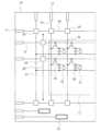
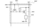
図1は表示装置を構成する、信号入力端子、走査線、信号線、非線形素子を含む保護回路
及び画素部の位置関係を説明する図である。絶縁表面を有する基板10上に走査線13と
信号線14が交差して画素部17が構成されている。FIG. 1 is a diagram for explaining the positional relationship among signal input terminals, scanning lines, signal lines, protection circuits including nonlinear elements, and pixel portions, which constitute a display device. A
画素部17は複数の画素18がマトリクス状に配列して構成されている。画素18は走査
線13と信号線14に接続する画素トランジスタ19、保持容量部20、画素電極21を
含んで構成されている。The
ここで例示する画素構成において、保持容量部20は一方の電極が画素トランジスタ19
と接続し、他方の電極が容量線22と接続する場合を示している。また、画素電極21は
表示素子(液晶素子、発光素子、コントラスト媒体(電子インク)など)を駆動する一方
の電極を構成する。これらの表示素子の他方の電極は共通端子23に接続される。In the pixel configuration illustrated here, one electrode of the
, and the other electrode is connected to the
保護回路は画素部17と、走査線入力端子11及び信号線入力端子12との間に配設され
ている。本形態では複数の保護回路を配設して、走査線13、信号線14及び容量バス線
27に静電気等によりサージ電圧が印加され、画素トランジスタ19などが破壊されない
ように構成されている。そのため、保護回路にはサージ電圧が印加されたときに、共通配
線29又は共通配線28に電荷を逃がすように構成されている。The protection circuit is arranged between the
本形態では、走査線13側に保護回路24、信号線14側に保護回路25、容量バス線2
7に保護回路26を配設する例を示している。尤も、保護回路の構成はこれに限定されな
い。In this embodiment, the
7 shows an example in which a
図2は保護回路の一例を示す。この保護回路は、走査線13に対して並列に配置された非
線形素子30及び非線形素子31によって構成されている。非線形素子30及び非線形素
子31は、ダイオードのような二端子素子又はトランジスタのような三端子素子で構成さ
れる。例えば、画素部の画素トランジスタと同じ工程で形成することも可能であり、例え
ばゲート端子とドレイン端子を接続することによりダイオードと同様の特性を持たせるこ
とができる。FIG. 2 shows an example of a protection circuit. This protection circuit is composed of a
非線形素子30の第1端子(ゲート)と第3端子(ドレイン)は走査線13に接続され、
第2端子(ソース)は共通配線29に接続されている。また、非線形素子31の第1端子
(ゲート)と第3端子(ドレイン)は共通配線29に接続され、第2端子(ソース)は走
査線13に接続されている。すなわち、図2で示す保護回路は、二つのトランジスタのそ
れぞれが、整流方向を互いに逆向きにして、走査線13と共通配線29を接続する構成で
ある。言い換えると、走査線13と共通配線29の間に、整流方向が走査線13から共通
配線29に向かうトランジスタと整流方向が共通配線29から走査線13に向かうトラン
ジスタを接続する構成である。A first terminal (gate) and a third terminal (drain) of the
A second terminal (source) is connected to the
図2で示す保護回路は、共通配線29に対し、走査線13が静電気等により正又は負に帯
電した場合、その電荷を打ち消す方向に電流が流れる。例えば、走査線13が正に帯電し
た場合は、その正電荷を共通配線29に逃がす方向に電流が流れる。この動作により、帯
電した走査線13に接続している画素トランジスタ19の静電破壊又はしきい値電圧のシ
フトを防止することができる。また、帯電している走査線13と絶縁層を介して交差する
他の配線との間で、絶縁膜の絶縁破壊を防止することができる。In the protection circuit shown in FIG. 2, when the
なお、図2は走査線13に第1端子(ゲート)を接続した非線形素子30と、共通配線2
9に第1端子(ゲート)を接続した非線形素子31、すなわち整流方向が逆向きの二個一
組の非線形素子を用い、それぞれの第2端子(ソース)と第3端子(ドレイン)で共通配
線29と走査線13を接続している。すなわち、非線形素子30と非線形素子31は並列
である。他の構成として、さらに並列して接続する非線形素子を付加して、保護回路の動
作安定性を高めても良い。例えば、図3は走査線13と共通配線29との間に設けられた
、非線形素子30aと非線形素子30b及び非線形素子31aと非線形素子31bにより
構成される保護回路を示す。この保護回路は、共通配線29に第1端子(ゲート)を接続
した二つの非線形素子(30b、31b)と、走査線13に第1端子(ゲート)を接続し
た二つの非線形素子(30a、31a)の計四つの非線形素子を用いている。すなわち、
整流方向が互いに逆向きになるよう2つの非線形素子を接続した一組を、共通配線29と
走査線13の間に二組接続している。言い換えると、走査線13と共通配線29の間に、
整流方向が走査線13から共通配線29に向かう2つのトランジスタと、整流方向が共通
配線29から走査線13に向かう2つのトランジスタを接続する構成である。このように
、共通配線29と走査線13を四つの非線形素子で接続することで、走査線13にサージ
電圧が印加された場合のみならず、共通配線29静電気等により帯電した場合であっても
、その電荷がそのまま走査線13に流れ込んでしまうのを防止することができる。なお、
図6に、4つの非線形素子740a、740b、740c、740dを基板上に配置する
場合の一態様を等価回路図と共に示す。ここで、符号650は走査線、符号651は共通
配線を示す。2 shows the
A
Two sets of two nonlinear elements are connected between the
Two transistors whose rectification direction is from the
FIG. 6 shows one aspect of arranging four
また、奇数個の非線形素子を使った保護回路の例として、非線形素子の基板への配置例を
図7(A)に、等価回路図を図7(B)に示す。この回路では非線形素子730cに対し
、非線形素子730b、非線形素子730aがスイッチング素子として接続している。こ
のように非線形素子を直列に接続することで、保護回路を構成する非線形素子に加わる瞬
間的な負荷を分散できる。ここで、符号650は走査線、符号651は共通配線を示す。As an example of a protection circuit using an odd number of nonlinear elements, an example of arrangement of nonlinear elements on a substrate is shown in FIG. 7A, and an equivalent circuit diagram is shown in FIG. 7B. In this circuit, a
図2は走査線13側に設ける保護回路の例を示すが、同様な構成の保護回路は信号線14
側においても適用することができる。FIG. 2 shows an example of a protection circuit provided on the
It can also be applied on the side.
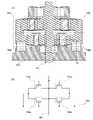
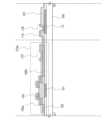
図4(A)は保護回路の一例を示す平面図であり、図4(B)はその等価回路図を示す。
また、図4(A)中に示されるQ1-Q2切断線に対応した断面図を図5に示す。以下の
説明では図4及び図5を参照して保護回路の一構成例を説明する。FIG. 4A is a plan view showing an example of a protection circuit, and FIG. 4B shows its equivalent circuit diagram.
FIG. 5 shows a cross-sectional view corresponding to the Q1-Q2 cutting line shown in FIG. 4(A). In the following description, one configuration example of the protection circuit will be described with reference to FIGS. 4 and 5. FIG.
非線形素子170a及び非線形素子170bは、走査線13と同じ層で形成されるゲート
電極101及びゲート電極16を有している。ゲート電極101及びゲート電極16上に
はゲート絶縁層102が形成されている。ゲート絶縁層102上には第1酸化物半導体層
103が形成され、第1酸化物半導体層103を介してゲート電極101上で相対するよ
うに第1配線層38及び第2配線層39が設けられている。ゲート絶縁層102は、酸化
シリコン又は酸化アルミニウムなどの酸化物で形成される。なお、非線形素子170a及
び非線形素子170bは主要部において同じ構成を有している。The
第1酸化物半導体層103は、相対する第1配線層38及び第2配線層39の下にゲート
絶縁膜を介してゲート電極101を被覆するように設けられている。すなわち第1酸化物
半導体層103は、ゲート電極101と重畳し、ゲート絶縁層102の上面部と第2酸化
物半導体層104aおよび104bの下面部と接するように設けられている。ここで、第
1配線層38は、第1酸化物半導体層103側から第2酸化物半導体層104aと導電層
105aが積層された構成を有している。同様に、第2配線層39は第1酸化物半導体層
103側から第2酸化物半導体層104bと導電層105bが積層された構成を有してい
る。The first
第1酸化物半導体層103の酸素濃度は第2酸化物半導体層(104aおよび104b)
よりも高い酸素濃度を有している。換言すれば、第1酸化物半導体層103は酸素過剰型
であり、第2酸化物半導体層(104aおよび104b)は酸素欠乏型である。第1酸化
物半導体層103の酸素濃度を高めることでドナー型欠陥を低減させることができ、キャ
リアのライフタイムや移動度が向上するといった効果が得られる。一方、第2酸化物半導
体層(104aおよび104b)は、酸素濃度を第1酸化物半導体層103と比べて低く
することでキャリア濃度を高めることができ、ソース領域及びドレイン領域を形成するた
めに利用することができる。The oxygen concentration of the first
has a higher oxygen concentration than In other words, the first
酸化物半導体の構造的には、第1酸化物半導体層103はIn、Ga、Zn、及びOを含
む非単結晶酸化物半導体層であり、少なくともアモルファス成分を含んでいるものとする
。第2酸化物半導体層(104aおよび104b)はIn、Ga、Zn、及びOを含む非
単結晶酸化物半導体層であり、非単結晶構造の中にナノクリスタルが含まれている場合が
ある。そして、第1酸化物半導体層103は第2酸化物半導体層(104aおよび104
b)よりも電気伝導度が低いという特性を有している。それゆえ、本形態の非線形素子1
70a及び非線形素子170bにおいて第2酸化物半導体層(104aおよび104b)
は、トランジスタのソース領域及びドレイン領域と同様の機能を発現する。ソース領域と
なる第2酸化物半導体層104a及びドレイン領域となる第2酸化物半導体層104bは
、n型の導電型を有し、活性化エネルギー(ΔE)が0.01eV以上0.1eV以下で
あり、n+領域とも呼べる。Structurally, the first
It has the property of lower electrical conductivity than b). Therefore, the
Second oxide semiconductor layers (104a and 104b) in 70a and
function similarly to the source and drain regions of a transistor. The second
第1酸化物半導体層103及び第2酸化物半導体層(104aおよび104b)は、酸化
物半導体として代表的には酸化亜鉛(ZnO)又は、In、Ga、及びZnを含む酸化物
半導体材料によって形成される。The first
第2酸化物半導体層(104a及び104b)は第1酸化物半導体層103と導電層(1
05a及び105b)に接してその間に設けられ、物性の異なる酸化物半導体層同士の接
合が形成されている。第1酸化物半導体層と導電層の間に第1酸化物半導体層103より
も電気伝導度が高い第2酸化物半導体層(104aおよび104b)を設けることにより
、第1酸化物半導体層と導電層が直接接するショットキー接合に比べて、非線形素子を安
定して動作させることが可能となる。すなわち、熱的安定性が増し、安定動作をさせるこ
とが可能となる。それにより保護回路の機能を高め動作の安定化を図ることができる。ま
た、接合リークが低減し、非線形素子170a及び非線形素子170bの特性を向上させ
ることができる。The second oxide semiconductor layers (104a and 104b) are the first
05a and 105b), and is provided between them to form a bond between oxide semiconductor layers having different physical properties. By providing the second oxide semiconductor layers (104a and 104b) having higher electrical conductivity than the first
第1酸化物半導体層103上には保護絶縁膜107が設けられている。保護絶縁膜107
は、酸化シリコン又は酸化アルミニウムなどの酸化物で形成される。また、酸化シリコン
又は酸化アルミニウム上に窒化シリコン、窒化アルミニウム、酸化窒化シリコン又は酸化
窒化アルミニウムを積層することで、保護膜としてより機能を高めることができる。A protective
is formed of an oxide such as silicon oxide or aluminum oxide. Further, by stacking silicon nitride, aluminum nitride, silicon oxynitride, or aluminum oxynitride over silicon oxide or aluminum oxide, the function as a protective film can be further enhanced.
いずれにしても、第1酸化物半導体層103と接する保護絶縁膜107を酸化物とするこ
とで、第1酸化物半導体層103から酸素が引き抜かれ、酸素欠乏型に変質してしまうこ
とを防ぐことができる。また、第1酸化物半導体層103が窒化物による絶縁層と直接的
に接しない構成とすることで、窒化物中の水素が拡散して第1酸化物半導体層103に水
酸基などに起因する欠陥を生成するのを防ぐことができる。In any case, by using an oxide for the protective
保護絶縁膜107にはコンタクトホール125および128が設けられており、ゲート電
極101と同じ層で形成される走査線13と、非線形素子170aの第三端子(ドレイン
)とが接続される。この接続は、画素部の画素電極と同じ材料で形成される第3配線層1
10で形成される。第3配線層110は、酸化インジウム・ズズ(ITO:indium
tin oxide)、酸化亜鉛(ZnO)、酸化スズ(SnO2)などの透明導電膜
で形成される。これにより第3配線層110は、金属材料で形成される配線と比べて高抵
抗化することになる。このような抵抗成分を含む配線を保護回路に含ませることで、過大
な電流が流れて非線形素子170aが破壊されるのを防ぐことができる。Contact holes 125 and 128 are provided in the protective
10. The
tin oxide), zinc oxide (ZnO), tin oxide (SnO2 ), or other transparent conductive film. As a result, the
なお、図4及び図5(A)では走査線13に設けられる保護回路の一例を示すが、同様の
保護回路を信号線、容量バス線などに適用することができる。Although FIGS. 4 and 5A show an example of a protection circuit provided for the
このように、本実施の形態によれば、酸化物半導体により構成される保護回路を設けるこ
とにより、保護回路として適した構造を有する表示装置を得ることができる。それにより
保護回路の機能を高め動作の安定化を図ることができる。As described above, according to this embodiment, by providing a protection circuit formed using an oxide semiconductor, a display device having a structure suitable for a protection circuit can be obtained. As a result, the function of the protection circuit can be improved and the operation can be stabilized.
(実施の形態2)
本形態は、実施の形態1において図4(A)に示した画素部とその周辺に非線形素子を含
む保護回路が形成された表示装置の作製工程の一様態を図8及び図9を参照して説明する
。図8及び図9は図4(A)中のQ1-Q2切断線に対応した断面図を表している。(Embodiment 2)
In this embodiment mode, one mode of a manufacturing process of a display device in which a protection circuit including a nonlinear element is formed in the pixel portion shown in FIG. to explain. 8 and 9 are sectional views corresponding to the Q1-Q2 section line in FIG. 4(A).
図8(A)において、透光性を有する基板100には市販されているバリウムホウケイ酸
ガラス、アルミノホウケイ酸ガラス及びアルミノシリケートガラスなどのガラス基板を用
いることができる。例えば、成分比としてホウ酸(B2O3)よりも酸化バリウム(Ba
O)を多く含み、歪み点が730℃以上のガラス基板を用いると好ましい。酸化物半導体
層を700℃程度の高温で熱処理する場合でも、ガラス基板が歪まないで済むからである
。In FIG. 8A, a commercially available glass substrate such as barium borosilicate glass, aluminoborosilicate glass, or aluminosilicate glass can be used as the light-transmitting
It is preferable to use a glass substrate containing a large amount of O) and having a strain point of 730° C. or higher. This is because the glass substrate is not distorted even when the oxide semiconductor layer is heat-treated at a high temperature of about 700°C.
次いで、導電層を基板100全面に形成した後、第1のフォトリソグラフィー工程を行い
、レジストマスクを形成し、エッチングにより不要な部分を除去して配線及び電極(ゲー
ト電極101を含むゲート配線、容量配線、及び端子)を形成する。このとき少なくとも
ゲート電極101の端部にテーパー形状が形成されるようにエッチングする。Next, after a conductive layer is formed over the entire surface of the
ゲート電極101を含むゲート配線と容量配線、端子部の端子は、アルミニウム(Al)
や銅(Cu)などの低抵抗導電性材料で形成することが望ましいが、Al単体では耐熱性
が劣り、また腐蝕しやすい等の問題点があるので耐熱性導電性材料と組み合わせて形成す
る。耐熱性導電性材料としては、チタン(Ti)、タンタル(Ta)、タングステン(W
)、モリブデン(Mo)、クロム(Cr)、Nd(ネオジム)、Sc(スカンジウム)か
ら選ばれた元素、または上述した元素を成分とする合金か、上述した元素を組み合わせた
合金膜、または上述した元素を成分とする窒化物で形成する。Aluminum (Al) is used for the gate wiring including the
Although it is desirable to form it with a low-resistance conductive material such as copper (Cu) or the like, Al alone has problems such as poor heat resistance and susceptibility to corrosion, so it is formed in combination with a heat-resistant conductive material. Titanium (Ti), tantalum (Ta), tungsten (W
), molybdenum (Mo), chromium (Cr), Nd (neodymium), and Sc (scandium), or an alloy containing the above elements as components, or an alloy film combining the above elements, or the above It is made of a nitride containing an element.
次いで、ゲート電極101上にゲート絶縁層102を全面に成膜する。ゲート絶縁層10
2はスパッタ法などを用い、膜厚を50~250nmとする。Next, a
2 uses a sputtering method or the like to have a film thickness of 50 to 250 nm.
例えば、ゲート絶縁層102としてスパッタ法により酸化シリコン膜を用い、100nm
の厚さで形成する。勿論、ゲート絶縁層102はこのような酸化シリコン膜に限定される
ものでなく、酸化窒化シリコン膜、窒化シリコン膜、酸化アルミニウム、酸化タンタル膜
などの他の絶縁膜を用い、これらの材料から成る単層または積層構造として形成しても良
い。For example, a silicon oxide film is used as the
thickness. Of course, the
次に、第1酸化物半導体膜を形成する前のゲート絶縁層102にプラズマ処理を行う。こ
こでは酸素ガスとアルゴンガスを成膜室に導入してプラズマを発生させる逆スパッタを行
い、ゲート絶縁層に酸素ラジカル又は酸素を照射する。こうして、表面に付着しているゴ
ミを除去し、さらにゲート絶縁層表面を酸素過剰領域に改質する。ゲート絶縁層の表面に
酸素ラジカル処理を行い、表面を酸素過剰領域とすることは、その後の工程での信頼性向
上のための熱処理(200℃~600℃)において、ゲート絶縁層と第1酸化物半導体層
の界面を改質するための酸素の供給源を作る上で有効である。Next, plasma treatment is performed on the
ゲート絶縁膜層、第1酸化物半導体膜、及び第2酸化物半導体膜は、スパッタ法で、チャ
ンバーに導入するガス並びに設置するターゲットを適宣切り替えることにより、ゲート絶
縁層、第1酸化物半導体膜、及び第2酸化物半導体膜を大気に触れることなく連続して成
膜できる。大気に触れることなく連続成膜すると、不純物の混入を防止することができる
。大気に触れることなく連続成膜する場合、マルチチャンバー方式の製造装置を用いるこ
とが好ましい。The gate insulating film layer, the first oxide semiconductor film, and the second oxide semiconductor film are formed by a sputtering method by appropriately switching the gas introduced into the chamber and the target to be set, thereby forming the gate insulating film layer, the first oxide semiconductor film, and the second oxide semiconductor film. A film and a second oxide semiconductor film can be formed continuously without being exposed to the air. Continuous film formation without exposure to the air can prevent contamination of impurities. In the case of continuous film formation without exposure to air, it is preferable to use a multi-chamber manufacturing apparatus.
特に、第1酸化物半導体膜に接するゲート絶縁層102と第1酸化物半導体膜は連続で成
膜するのが望ましい。連続成膜することで、水蒸気などの大気成分や大気中に浮遊する不
純物元素やゴミによる汚染がない積層界面を形成できるので、非線形素子および薄膜トラ
ンジスタの特性のばらつきを低減できる。In particular, it is preferable to continuously form the
なお、本明細書中で連続成膜とは、スパッタ法で行う第1の成膜工程からスパッタ法で行
う第2の成膜工程までの一連のプロセス中、被処理基板の置かれている雰囲気が大気等の
汚染雰囲気に触れることなく、常に真空中または不活性ガス雰囲気(窒素雰囲気または希
ガス雰囲気)で制御されていることを言う。連続成膜を行うことにより、清浄化された被
処理基板の水分等の再付着を回避して成膜を行うことができる。In this specification, the term "continuous film formation" refers to the atmosphere in which the substrate to be processed is placed during a series of processes from the first film formation process performed by the sputtering method to the second film formation process performed by the sputtering method. is always controlled in a vacuum or an inert gas atmosphere (nitrogen atmosphere or rare gas atmosphere) without being exposed to a contaminated atmosphere such as air. By performing continuous film formation, film formation can be performed while avoiding reattachment of moisture or the like to the cleaned substrate to be processed.
次いで、プラズマ処理された基板を大気に曝すことなく第1酸化物半導体膜を成膜する。
プラズマ処理された基板を大気に曝すことなく第1酸化物半導体膜を成膜することにより
、ゲート絶縁層と半導体膜の界面にゴミや水分が付着する不具合を防ぐことができる。こ
こでは、直径8インチのIn、Ga、及びZnを含む酸化物半導体ターゲット(組成比と
して、In2O3:Ga2O3:ZnO=1:1:1)を用いて、基板とターゲットの間
との距離を170mm、圧力0.4Pa、直流(DC)電源0.5kW、酸素雰囲気下で
成膜する。なお、パルス直流(DC)電源を用いると、ごみが軽減でき、膜厚分布も均一
となるために好ましい。第1酸化物半導体膜の膜厚は、5nm~200nmとする。本実
施の形態では第1酸化物半導体膜の膜厚は、100nmとする。Next, a first oxide semiconductor film is formed without exposing the plasma-treated substrate to the air.
By forming the first oxide semiconductor film without exposing the plasma-treated substrate to the atmosphere, the problem of dust or moisture adhering to the interface between the gate insulating layer and the semiconductor film can be prevented. Here, an oxide semiconductor target containing In, Ga, and Zn with a diameter of 8 inches (In2 O3 :Ga2 O3 :ZnO=1:1:1 as a composition ratio) was used, and The film is formed under an oxygen atmosphere with a distance of 170 mm, a pressure of 0.4 Pa, a direct current (DC) power source of 0.5 kW. A pulse direct current (DC) power source is preferably used because dust can be reduced and the film thickness distribution can be uniform. The thickness of the first oxide semiconductor film is set to 5 nm to 200 nm. In this embodiment, the thickness of the first oxide semiconductor film is 100 nm.
第1酸化物半導体膜は、第2酸化物半導体膜の成膜条件と異ならせることで、第2酸化物
半導体膜と異なる組成を有する。一例として、第2酸化物半導体膜中の酸素濃度より多く
の酸素を第1酸化物半導体膜中に含ませる。例えば、第2酸化物半導体膜の成膜条件にお
ける酸素ガス流量とアルゴンガス流量の比よりも第1酸化物半導体膜の成膜条件における
酸素ガス流量の占める比率が多い条件とする。具体的には、第2酸化物半導体膜の成膜条
件は、希ガス(アルゴン、又はヘリウムなど)雰囲気下(または酸素ガス10%以下、ア
ルゴンガス90%以上)とし、第1酸化物半導体膜の成膜条件は、酸素雰囲気下(又は酸
素ガス流量がアルゴンガス流量以上であって、その比が1:1以上)とする。多くの酸素
を第1酸化物半導体膜中に含ませることによって、第2酸化物半導体膜よりも導電率を低
くすることができる。また、多くの酸素を第1酸化物半導体膜中に含ませることによって
オフ電流の低減を図ることができるため、オン・オフ比の高い薄膜トランジスタを得るこ
とができる。The first oxide semiconductor film has a composition different from that of the second oxide semiconductor film by making the film formation conditions different from those of the second oxide semiconductor film. As an example, the oxygen concentration in the first oxide semiconductor film is higher than that in the second oxide semiconductor film. For example, the ratio of the oxygen gas flow rate under the deposition conditions of the first oxide semiconductor film is higher than the ratio of the oxygen gas flow rate to the argon gas flow rate under the deposition conditions of the second oxide semiconductor film. Specifically, the deposition conditions for the second oxide semiconductor film are a rare gas (argon, helium, or the like) atmosphere (or oxygen gas of 10% or less, argon gas of 90% or more), and the first oxide semiconductor film is The film formation conditions for 1 are an oxygen atmosphere (or the oxygen gas flow rate is greater than or equal to the argon gas flow rate, and the ratio is 1:1 or greater). By including a large amount of oxygen in the first oxide semiconductor film, the conductivity can be lower than that of the second oxide semiconductor film. In addition, since a large amount of oxygen is contained in the first oxide semiconductor film, off-state current can be reduced, so that a thin film transistor with a high on/off ratio can be obtained.
なお、第1酸化物半導体膜の成膜は、先に逆スパッタを行ったチャンバーと同一チャンバ
ーを用いてもよいし、大気に曝すことなく成膜できるのであれば、先に逆スパッタを行っ
たチャンバーと異なるチャンバーで成膜してもよい。Note that the first oxide semiconductor film may be formed in the same chamber as the chamber in which the reverse sputtering was previously performed, or if the film can be formed without exposure to the atmosphere, the reverse sputtering is performed first. A film may be formed in a chamber different from the chamber.
次に、第1酸化物半導体膜上に第2酸化物半導体膜をスパッタ法で成膜する。ここでは、
酸化インジウム(In2O3)と、酸化ガリウム(Ga2O3)と、酸化亜鉛(ZnO)
の組成比を1:1:1(=In2O3:Ga2O3:ZnO)としたターゲットを用いて
、基板とターゲットの間との距離を170mm、成膜室の圧力を0.4Pa、直流(DC
)電源0.5kW、成膜温度を室温とし、アルゴンガス流量40sccmを導入してスパ
ッタ成膜を行う。これにより、第2酸化物半導体膜として、In、Ga、Zn及び酸素を
成分とする半導体膜が形成される。組成比を1:1:1(=In2O3:Ga2O3:Z
nO)としたターゲットを意図的に用いているにも関わらず、成膜直後で大きさ1nm~
10nmの結晶粒を含む酸化物半導体膜がしばしば形成される。なお、ターゲットの成分
比、成膜圧力(0.1Pa~2.0Pa)、電力(250W~3000W:8インチφ)
、温度(室温~100℃)、反応性スパッタの成膜条件などを適宜調節することで結晶粒
の有無や、結晶流の密度や、直径サイズは、1nm~10nmの範囲で調節されうると言
える。第2酸化物半導体膜の膜厚は、5nm~20nmとする。勿論、膜中に結晶粒が含
まれる場合、含まれる結晶粒のサイズが膜厚を超える大きさとならない。本実施の形態で
は第2酸化物半導体膜の膜厚は、5nmとする。Next, a second oxide semiconductor film is formed over the first oxide semiconductor film by a sputtering method. here,
Indium oxide (In2O3 ),gallium oxide (Ga2O3) , and zinc oxide (ZnO)
A composition ratio of 1:1:1 (=In2 O3 :Ga2 O3 :ZnO) was used, the distance between the substrate and the target was 170 mm, and the pressure in the deposition chamber was 0.4 Pa. , direct current (DC
) A power source of 0.5 kW, a deposition temperature of room temperature, and an argon gas flow rate of 40 sccm are introduced to perform sputtering deposition. As a result, a semiconductor film containing In, Ga, Zn, and oxygen as components is formed as the second oxide semiconductor film. A composition ratio of 1:1:1 (=In2 O3 :Ga2 O3 :Z
nO) target was intentionally used, the size of 1 nm ~
An oxide semiconductor film containing 10-nm crystal grains is often formed. In addition, the component ratio of the target, film formation pressure (0.1 Pa to 2.0 Pa), power (250 W to 3000 W: 8 inches φ)
, temperature (room temperature to 100° C.), film formation conditions for reactive sputtering, etc. can be adjusted appropriately to control the presence or absence of crystal grains, the density of crystal flow, and the diameter size within the range of 1 nm to 10 nm. . The thickness of the second oxide semiconductor film is set to 5 nm to 20 nm. Of course, when crystal grains are contained in the film, the size of the crystal grains contained does not exceed the film thickness. In this embodiment, the thickness of the second oxide semiconductor film is 5 nm.
次に、第2のフォトリソグラフィー工程を行い、レジストマスクを形成し、第1酸化物半
導体膜および第2酸化物半導体膜をエッチングする。ここではITO07N(関東化学社
製)を用いたウェットエッチングにより、不要な部分を除去して第1酸化物半導体層10
3および第2酸化物半導体層111を形成する。なお、ここでのエッチングは、ウェット
エッチングに限定されずドライエッチングを用いてもよい。この段階での断面図を図8(
B)に示した。Next, a second photolithography step is performed to form a resist mask, and the first oxide semiconductor film and the second oxide semiconductor film are etched. Here, by wet etching using ITO07N (manufactured by Kanto Kagaku Co., Ltd.), unnecessary portions are removed to remove the first
3 and a second
B).
次に、第2酸化物半導体層111およびゲート絶縁層102上に金属材料からなる導電膜
132をスパッタ法や真空蒸着法で形成する。導電膜132の材料としては、Al、Cr
、Ta、Ti、Mo、Wから選ばれた元素、または上述した元素を成分とする合金か、上
述した元素を組み合わせた合金膜等が挙げられる。Next, a
, Ta, Ti, Mo, and W, an alloy containing the above-described elements, or an alloy film obtained by combining the above-described elements.
また、200℃~600℃の熱処理を行う場合には、この熱処理に耐える耐熱性を導電膜
に持たせることが好ましい。Al単体では耐熱性が劣り、また腐蝕しやすい等の問題点が
あるので耐熱性導電性材料と組み合わせて形成する。Alと組み合わせる耐熱性導電性材
料としては、チタン(Ti)、タンタル(Ta)、タングステン(W)、モリブデン(M
o)、クロム(Cr)、Nd(ネオジム)、Sc(スカンジウム)から選ばれた元素、ま
たは上述した元素を成分とする合金か、上述した元素を組み合わせた合金膜、または上述
した元素を成分とする窒化物で形成する。Further, when heat treatment is performed at 200° C. to 600° C., it is preferable that the conductive film has heat resistance to withstand the heat treatment. Since Al alone has problems such as poor heat resistance and susceptibility to corrosion, it is formed in combination with a heat-resistant conductive material. Heat-resistant conductive materials combined with Al include titanium (Ti), tantalum (Ta), tungsten (W), molybdenum (M
o) an element selected from chromium (Cr), Nd (neodymium), and Sc (scandium), or an alloy containing the above elements as components, or an alloy film combining the above elements, or It is made of a nitride that
ここでは、導電膜132としてTi膜と、そのTi膜上に重ねてNdを含むアルミニウム
(Al-Nd)膜を積層し、さらにその上にTi膜を成膜する3層構造とする。また、導
電膜132は、2層構造としてもよく、アルミニウム膜上にチタン膜を積層してもよい。
また、導電膜132は、シリコンを含むアルミニウム膜の単層構造や、チタン膜の単層構
造としてもよい。この段階での断面図を図8(C)に示した。Here, the
Alternatively, the
次に、第3のフォトリソグラフィー工程を行い、レジストマスク131を形成し、エッチ
ングにより導電膜132の不要な部分を除去して導電層105a及び105bを形成する
(図9(A)参照)。この際のエッチング方法としてウェットエッチングまたはドライエ
ッチングを用いる。ここでは、SiCl4とCl2とBCl3の混合ガスを反応ガスとし
たドライエッチングを用い、Ti膜とNdを含むアルミニウム(Al-Nd)膜とTi膜
を順次積層した導電膜をエッチングして導電層105a及び105bを形成する。Next, a third photolithography step is performed to form a resist
次に、導電膜132のエッチング工程に用いたものと同じレジストマスクを用いて、第2
酸化物半導体膜をエッチングする。ここではITO07N(関東化学社製)を用いたウェ
ットエッチングにより、不要な部分を除去して第2酸化物半導体層104a、104bを
形成する。なお、ここでのエッチングは、ウェットエッチングに限定されずドライエッチ
ングを用いてもよい。また、エッチング条件にもよるが第2酸化物半導体層111のエッ
チング工程において、第1酸化物半導体層103の露出領域も一部エッチングされる。よ
って第2酸化物半導体層104a、104bの間の第1酸化物半導体層103のチャネル
形成領域は図9(A)に示すように膜厚の薄い領域となる。Next, using the same resist mask as that used in the etching step of the
The oxide semiconductor film is etched. Here, unnecessary portions are removed by wet etching using ITO07N (manufactured by Kanto Kagaku Co., Ltd.) to form the second
さらに、第1酸化物半導体層103に酸素プラズマ処理を行ってもよい。プラズマ処理を
行うことにより、第1酸化物半導体層103のエッチングによるダメージを回復すること
ができる。代表的な酸素プラズマ処理は、酸素ガスのグロー放電プラズマで生成されたラ
ジカルで酸化物半導体の表面を処理することであるが、プラズマを生成するガスとしては
酸素のみでなく、酸素ガスと希ガスの混合ガスであってもよい。Further, oxygen plasma treatment may be performed on the first
次いで、200℃~600℃、代表的には300℃~500℃の熱処理を行うことが好ま
しい。ここでは炉に入れ、窒素雰囲気下で350℃、1時間の熱処理を行う。この熱処理
によりIn、Ga、及びZnを含む半導体膜の原子レベルの再配列が行われる。この熱処
理によりキャリアの移動を阻害する歪が解放されるため、ここでの熱処理(光アニールも
含む)は重要である。なお、熱処理を行うタイミングは、第1酸化物半導体膜の成膜後で
あれば特に限定されず、例えば保護膜形成後に行ってもよい。以上の工程で第1酸化物半
導体層103をチャネル形成領域とする非線形素子170aが作製できる。この段階での
断面図を図9(A)に示す。Then, it is preferable to perform heat treatment at 200°C to 600°C, typically 300°C to 500°C. Here, it is placed in a furnace and heat-treated at 350° C. for 1 hour in a nitrogen atmosphere. This heat treatment causes rearrangement at the atomic level in the semiconductor film containing In, Ga, and Zn. This heat treatment (including optical annealing) is important because the heat treatment releases the strain that inhibits carrier movement. Note that the timing of the heat treatment is not particularly limited as long as it is performed after the formation of the first oxide semiconductor film; for example, the heat treatment may be performed after the formation of the protective film. Through the above steps, the
次いで、レジストマスクを除去し、In、Ga、及びZnを含む半導体層を覆う保護絶縁
膜107を形成する。保護絶縁膜107はスパッタ法などを用いて得られる窒化シリコン
膜、酸化シリコン膜、酸化窒化シリコン膜、酸化アルミニウム膜、酸化タンタル膜などを
用いることができる。Next, the resist mask is removed, and a protective
次に、第4のフォトリソグラフィー工程を行い、レジストマスクを形成し、保護絶縁膜1
07のエッチングにより導電層105bに達するコンタクトホール125を形成する。な
お、マスク数を削減するため、同じレジストマスクを用いてさらにゲート絶縁層102を
エッチングしてゲート電極に達するコンタクトホール128も同じレジストマスクで形成
することが好ましい。この段階での断面図を図9(B)に示す。Next, a fourth photolithography process is performed to form a resist mask, and a protective
07 is etched to form a
次いで、レジストマスクを除去した後、透明導電膜を成膜する。透明導電膜の材料として
は、酸化インジウム(In2O3)や酸化インジウム酸化スズ合金(In2O3―SnO
2、ITOと略記する)などをスパッタ法や真空蒸着法などを用いて形成する。このよう
な材料のエッチング処理は塩酸系の溶液により行う。しかし、特にITOのエッチングは
残渣が発生しやすいので、エッチング加工性を改善するために酸化インジウム酸化亜鉛合
金(In2O3―ZnO)を用いても良い。After removing the resist mask, a transparent conductive film is formed. Materials for the transparent conductive film include indium oxide (In2 O3 ) and indium tin oxide alloy (In2 O3 —SnO 3 ).
2 , abbreviated as ITO) is formed by sputtering, vacuum deposition, or the like. Such materials are etched using a hydrochloric acid-based solution. However, since the etching of ITO is particularly prone to leaving residues, an alloy of indium oxide and zinc oxide (In2 O3 —ZnO) may be used to improve etching workability.
次に、第5のフォトリソグラフィー工程を行い、レジストマスクを形成し、エッチングに
より透明導電膜の不要な部分を除去して図示していない画素電極を形成する。Next, a fifth photolithography process is performed to form a resist mask, and an unnecessary portion of the transparent conductive film is removed by etching to form a pixel electrode (not shown).
また、この第5のフォトリソグラフィー工程において、図示していない容量部におけるゲ
ート絶縁層102及び保護絶縁膜107を誘電体として、容量配線と画素電極とで保持容
量が形成される。In the fifth photolithography process, the storage capacitor is formed by the capacitor wiring and the pixel electrode, using the
また、この第5のフォトリソグラフィー工程において、レジストマスクで端子部を覆い端
子部に形成された透明導電膜を残す。透明導電膜はFPCとの接続に用いられる電極また
は配線や、ソース配線の入力端子として機能する接続用の端子電極などになる。In the fifth photolithography step, the terminal portion is covered with a resist mask to leave the transparent conductive film formed on the terminal portion. The transparent conductive film becomes an electrode or wiring used for connection with the FPC, a terminal electrode for connection functioning as an input terminal of the source wiring, or the like.
また、本実施の形態においては、透明導電膜からなる第3配線層110が非線形素子17
0aのドレイン電極となる導電層105bと走査線108をコンタクトホール125およ
び128を介して接続し、保護回路を形成する。Further, in the present embodiment, the
A
次いで、レジストマスクを除去する。この段階での断面図を図9(C)に示す。Next, the resist mask is removed. A cross-sectional view at this stage is shown in FIG.
こうして5回のフォトリソグラフィー工程により、5枚のフォトマスクを使用して、複数
の非線形素子を有する(本実施の形態では、170aおよび170bの二つの非線形素子
を有する)保護回路を完成させることができる。非線形素子の第1酸化物半導体層と配線
層との接続構造において、第1酸化物半導体層よりも電気伝導度が高い第2酸化物半導体
層と接合する領域を設けることで、金属配線のみの場合に比べて、安定動作をさせること
が可能となる。それにより保護回路の機能を高め動作の安定化を図ることができる。また
、本実施の形態によれば、非線形素子の形成と共に、同様な方法で複数のTFTを作製で
きるので、ボトムゲート型のnチャネル型TFTを有する画素部の作製と保護回路の作製
を同時におこなうことができる。すなわち、本実施の形態に示した工程に従えば、薄膜の
剥がれに起因する保護回路の不良の少ない保護ダイオードを搭載したアクティブマトリク
ス型の表示装置用基板を作製することができる。In this way, a protection circuit having a plurality of nonlinear elements (in this embodiment, having two
(実施の形態3)
本形態は、画素部とその周辺に非線形素子を含む保護回路が形成された表示装置の実施の
形態2とは異なる一様態を、図27を参照して説明する。(Embodiment 3)
In this embodiment mode, a display device in which a protection circuit including a nonlinear element is formed in a pixel portion and its periphery, which is different from
図27は同一基板上に画素部に配置する薄膜トランジスタと非線形素子を含む保護回路が
形成された表示装置の断面構造を示す図である。非線形素子270aは第1酸化物半導体
層103にソース電極及びドレイン電極となる導電層(105a、105b)が接して設
けられている。FIG. 27 is a diagram showing a cross-sectional structure of a display device in which a thin film transistor and a protection circuit including a nonlinear element arranged in a pixel portion are formed on the same substrate. In the
非線形素子270aにおいて、プラズマ処理によって改質された第1酸化物半導体層10
3に導電層105a及び導電層105bが接している構成が好ましい。本実施の形態では
、導電膜を形成する前に、第1酸化物半導体層103にプラズマ処理を行う。In the
3 is preferably in contact with the
プラズマ処理としては、例えば逆スパッタ処理をその一例に挙げることができる。プラズ
マ処理は、アルゴンガス、水素ガス、アルゴン及び水素の混合ガス、を用いることができ
る。また上記ガスに酸素ガスを含ませてもよい。またアルゴンガスに変えて他の希ガスを
用いてもよい。An example of plasma processing is reverse sputtering. Plasma treatment can use argon gas, hydrogen gas, and mixed gases of argon and hydrogen. Further, oxygen gas may be included in the above gas. Also, other rare gas may be used instead of argon gas.
導電膜をエッチングして、ソース電極及びドレイン電極となる導電層(105a、105
b)を形成する。本実施の形態では、チタン膜をアンモニア過水(過酸化水素:アンモニ
ア:水=5:2:2)等によりウェットエッチングして、ソース電極及びドレイン電極と
なる導電層(105a、105b)を形成する。このエッチング工程において、In、G
a、及びZnを含む第1酸化物半導体層の露出領域の一部がエッチングされる。よって、
導電層105aと導電層105bの間に挟まれた領域、すなわち第1酸化物半導体層10
3のチャネル形成領域は図27のごとく膜厚の薄い領域となる。By etching the conductive film, conductive layers (105a, 105) to be source and drain electrodes are formed.
b). In this embodiment mode, the titanium film is wet-etched with ammonia hydrogen peroxide (hydrogen peroxide:ammonia:water=5:2:2) or the like to form conductive layers (105a and 105b) that serve as source and drain electrodes. do. In this etching process, In, G
Part of the exposed region of the first oxide semiconductor layer containing a and Zn is etched. Therefore,
A region sandwiched between the
A channel forming region 3 is a thin region as shown in FIG.
プラズマ処理により改質された第1酸化物半導体層103に接してソース電極及びドレイ
ン電極となる導電層(105a、105b)を形成することによって、第1酸化物半導体
層103とソース電極及びドレイン電極となる導電層(105a、105b)とのコンタ
クト抵抗を低減することができる。また、プラズマ処理により第1酸化物半導体層103
とソース電極及びドレイン電極となる導電層(105a、105b)の接合強度が高まり
薄膜の剥がれに起因する不良が起こりにくくなる。By forming conductive layers (105a and 105b) to be a source electrode and a drain electrode in contact with the first
The bonding strength of the conductive layers (105a, 105b) serving as the source electrode and the drain electrode is increased, and defects due to peeling of the thin film are less likely to occur.
以上の工程により、非線形素子半導体装置として信頼性の高い保護回路を有した表示装置
を作製することができる。Through the above steps, a display device having a highly reliable protection circuit can be manufactured as a nonlinear element semiconductor device.
(実施の形態4)
本実施の形態では、本発明の一態様を適用した表示装置として、保護回路と画素部に配置
するTFTを同一基板上に有する電子ペーパーの例を示す。(Embodiment 4)
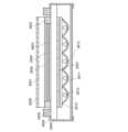
In this embodiment, as a display device to which one embodiment of the present invention is applied, an example of electronic paper in which a protection circuit and a TFT provided in a pixel portion are formed over the same substrate will be described.
図10は、本発明の一態様を適用した表示装置の例としてアクティブマトリクス型の電子
ペーパーを示す。半導体装置に用いられる薄膜トランジスタ581としては、実施の形態
2で示す非線形素子と同様に作製でき、In、Ga、及びZnを含む酸化物半導体を半導
体層並びにソース領域及びドレイン領域に用いた電気特性の高い薄膜トランジスタである
。FIG. 10 illustrates active matrix electronic paper as an example of a display device to which one embodiment of the present invention is applied. The
図10の電子ペーパーは、ツイストボール表示方式を用いた表示装置の例である。ツイス
トボール表示方式とは、白と黒に塗り分けられた球形粒子を表示素子に用いる電極層であ
る第1の電極層及び第2の電極層の間に配置し、第1の電極層及び第2の電極層に電位差
を生じさせての球形粒子の向きを制御することにより、表示を行う方法である。The electronic paper in FIG. 10 is an example of a display device using a twist ball display method. In the twist ball display method, spherical particles separately painted in white and black are arranged between a first electrode layer and a second electrode layer, which are electrode layers used in a display element, and the first electrode layer and the second electrode layer are arranged. In this method, display is performed by controlling the orientation of spherical particles by generating a potential difference between two electrode layers.
薄膜トランジスタ581はボトムゲート構造の薄膜トランジスタであり、ソース電極層又
はドレイン電極層が第1の電極層587と、絶縁層に形成される開口を介して電気的に接
続している。第1の電極層587と第2の電極層588との間には黒色領域590a及び
白色領域590bを有し、周りに液体で満たされているキャビティ594を含む球形粒子
589が設けられており、球形粒子589の周囲は樹脂等の充填材595で充填されてい
る(図10参照。)。The
また、ツイストボールの代わりに、電気泳動素子を用いることも可能である。透明な液体
と、正に帯電した白い微粒子と負に帯電した黒い微粒子とを封入した直径10μm~20
0μm程度のマイクロカプセルを用いる。第1の電極層と第2の電極層との間に設けられ
るマイクロカプセルは、第1の電極層と第2の電極層によって、電場が与えられると、白
い微粒子と、黒い微粒子が逆の方向に移動し、白または黒を表示することができる。この
原理を応用した表示素子が電気泳動表示素子であり、一般的に電子ペーパーとよばれてい
る。電気泳動表示素子は、液晶表示素子に比べて反射率が高いため、補助ライトは不要で
あり、また消費電力が小さく、薄暗い場所でも表示部を認識することが可能である。また
、表示部に電源が供給されない場合であっても、一度表示した像を保持することが可能で
ある。従って、例えば電源供給源となる電波発信源から表示機能付き半導体装置(単に表
示装置、又は表示装置を具備する半導体装置ともいう)を遠ざけた場合であっても、表示
された像を保存しておくことが可能となる。Also, an electrophoresis element can be used instead of the twist ball. 10 μm to 20 μm in diameter containing transparent liquid, positively charged white fine particles and negatively charged black fine particles
Microcapsules of about 0 μm are used. In the microcapsules provided between the first electrode layer and the second electrode layer, when an electric field is applied by the first electrode layer and the second electrode layer, white fine particles and black fine particles are oriented in opposite directions. Can move to and display white or black. A display device to which this principle is applied is an electrophoretic display device, and is generally called electronic paper. Since the electrophoretic display element has a higher reflectance than the liquid crystal display element, it does not require an auxiliary light, consumes less power, and can be recognized even in a dimly lit place. Further, even when power is not supplied to the display portion, it is possible to hold an image once displayed. Therefore, for example, even when a semiconductor device with a display function (also referred to simply as a display device or a semiconductor device having a display device) is moved away from a radio wave source that serves as a power supply source, the displayed image can be saved. It becomes possible to put
以上の工程により、非線形素子の第1酸化物半導体層と配線層との接続構造において、第
1酸化物半導体層よりも電気伝導度が高い第2酸化物半導体層と接合する領域を設けるこ
とで、金属配線のみの場合に比べて、安定動作をさせることが可能となる。それにより保
護回路の機能を高め動作の安定化を図ることができる。また、動作の安定化が図られ、薄
膜の剥がれに起因する不良が起こりにくい非線形素子からなる保護回路を搭載した信頼性
の高い電子ペーパーを作製することができる。Through the above steps, in the connection structure between the first oxide semiconductor layer and the wiring layer of the nonlinear element, a region to be bonded to the second oxide semiconductor layer having higher electrical conductivity than the first oxide semiconductor layer is provided. , it is possible to operate more stably than in the case of using only metal wiring. As a result, the function of the protection circuit can be improved and the operation can be stabilized. In addition, it is possible to manufacture highly reliable electronic paper equipped with a protective circuit including a nonlinear element that stabilizes the operation and makes it difficult for defects caused by peeling of the thin film to occur.
本実施の形態は、他の実施の形態に記載した構成と適宜組み合わせて実施することが可能
である。This embodiment can be implemented in appropriate combination with any structure described in any of the other embodiments.
(実施の形態5)
本実施の形態では、本発明の一態様の半導体装置の一例である表示装置において、同一基
板上に少なくとも保護回路と、駆動回路の一部と、画素部に配置する薄膜トランジスタを
作製する例について図11乃至図16を用いて以下に説明する。(Embodiment 5)
In this embodiment, in a display device which is an example of a semiconductor device of one embodiment of the present invention, at least a protection circuit, part of a driver circuit, and a thin film transistor provided in a pixel portion are manufactured over one substrate. 11 to 16 will be used to explain.
保護回路と同一基板上の画素部に配置する薄膜トランジスタは、実施の形態2又は3で示
す非線形素子と同様に形成する。また、形成した薄膜トランジスタはnチャネル型TFT
であるため、駆動回路のうち、nチャネル型TFTで構成することができる駆動回路の一
部を画素部の薄膜トランジスタと同一基板上に形成する。A thin film transistor provided in a pixel portion over the same substrate as the protection circuit is formed in the same manner as the nonlinear element described in
Therefore, part of the driver circuit which can be formed of n-channel TFTs is formed over the same substrate as the thin film transistors in the pixel portion.
本発明の一態様の半導体装置の一例であるアクティブマトリクス型液晶表示装置のブロッ
ク図の一例を図11(A)に示す。図11(A)に示す表示装置は、基板5300上に表
示素子を備えた画素を複数有する画素部5301と、各画素を選択する走査線駆動回路5
302と、選択された画素へのビデオ信号の入力を制御する信号線駆動回路5303とを
有する。FIG. 11A shows an example of a block diagram of an active matrix liquid crystal display device which is an example of a semiconductor device of one embodiment of the present invention. A display device shown in FIG.
302 and a signal line driver circuit 5303 for controlling input of video signals to selected pixels.
画素部5301は、信号線駆動回路5303から列方向に伸張して配置された複数の信号
線S1~Sm(図示せず。)により信号線駆動回路5303と接続され、走査線駆動回路
5302から行方向に伸張して配置された複数の走査線G1~Gn(図示せず。)により
走査線駆動回路5302と接続され、信号線S1~Sm並びに走査線G1~Gnに対応し
てマトリクス状に配置された複数の画素(図示せず。)を有する。そして、各画素は、信
号線Sj(信号線S1~Smのうちいずれか一)、走査線Gi(走査線G1~Gnのうち
いずれか一)と接続される。The pixel portion 5301 is connected to the signal line driver circuit 5303 by a plurality of signal lines S1 to Sm (not shown) extending in the column direction from the signal line driver circuit 5303, and is connected to the scanning
また、実施の形態2又は3で示す非線形素子と共に同様の方法で形成できる薄膜トランジ
スタは、nチャネル型TFTであり、nチャネル型TFTで構成する信号線駆動回路につ
いて図12を用いて説明する。Thin film transistors that can be formed by a method similar to the nonlinear element described in
図12に示す信号線駆動回路は、ドライバIC5601、スイッチ群5602_1~56
02_M、第1の配線5611、第2の配線5612、第3の配線5613及び配線56
21_1~5621_Mを有する。スイッチ群5602_1~5602_Mそれぞれは、
第1の薄膜トランジスタ5603a、第2の薄膜トランジスタ5603b及び第3の薄膜
トランジスタ5603cを有する。The signal line driving circuit shown in FIG. 12 includes a
02_M, the
21_1 to 5621_M. Each of the switch groups 5602_1 to 5602_M
It has a first
ドライバIC5601は第1の配線5611、第2の配線5612、第3の配線5613
及び配線5621_1~5621_Mに接続される。そして、スイッチ群5602_1~
5602_Mそれぞれは、第1の配線5611、第2の配線5612、第3の配線561
3及びスイッチ群5602_1~5602_Mそれぞれに対応した配線5621_1~5
621_Mに接続される。そして、配線5621_1~5621_Mそれぞれは、第1の
薄膜トランジスタ5603a、第2の薄膜トランジスタ5603b及び第3の薄膜トラン
ジスタ5603cを介して、3つの信号線に接続される。例えば、J列目の配線5621
_J(配線5621_1~配線5621_Mのうちいずれか一)は、スイッチ群5602
_Jが有する第1の薄膜トランジスタ5603a、第2の薄膜トランジスタ5603b及
び第3の薄膜トランジスタ5603cを介して、信号線Sj-1、信号線Sj、信号線S
j+1に接続される。The
and wirings 5621_1 to 5621_M. Then, switch group 5602_1 to
Each of 5602_M includes a
3 and wires 5621_1 to 5 corresponding to switch groups 5602_1 to 5602_M, respectively.
621_M. Each of the wirings 5621_1 to 5621_M is connected to three signal lines through the first
_J (one of the wirings 5621_1 to 5621_M) is connected to the switch group 5602
Through the first
なお、第1の配線5611、第2の配線5612、第3の配線5613には、それぞれ信
号が入力される。Note that signals are input to the
なお、ドライバIC5601は、単結晶基板上に形成されていることが望ましい。さらに
、スイッチ群5602_1~5602_Mは、画素部と同一基板上に形成されていること
が望ましい。したがって、ドライバIC5601とスイッチ群5602_1~5602_
MとはFPCなどを介して接続するとよい。Note that the
It is preferable to connect to M via an FPC or the like.
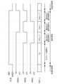
次に、図12に示した信号線駆動回路の動作について、図13のタイミングチャートを参
照して説明する。なお、図13のタイミングチャートは、i行目の走査線Giが選択され
ている場合のタイミングチャートを示している。さらに、i行目の走査線Giの選択期間
は、第1のサブ選択期間T1、第2のサブ選択期間T2及び第3のサブ選択期間T3に分
割されている。さらに、図12の信号線駆動回路は、他の行の走査線が選択されている場
合でも図13と同様の動作をする。Next, the operation of the signal line driver circuit shown in FIG. 12 will be described with reference to the timing chart of FIG. Note that the timing chart of FIG. 13 shows a timing chart when the i-th scanning line Gi is selected. Furthermore, the selection period of the i-th scanning line Gi is divided into a first sub-selection period T1, a second sub-selection period T2 and a third sub-selection period T3. Furthermore, the signal line driving circuit in FIG. 12 operates in the same manner as in FIG. 13 even when scanning lines in other rows are selected.
なお、図13のタイミングチャートは、J列目の配線5621_Jが第1の薄膜トランジ
スタ5603a、第2の薄膜トランジスタ5603b及び第3の薄膜トランジスタ560
3cを介して、信号線Sj-1、信号線Sj、信号線Sj+1に接続される場合について
示している。Note that in the timing chart of FIG. 13, the J-th wiring 5621_J is the first
3c, the signal line Sj−1, the signal line Sj, and the signal line Sj+1 are connected.
なお、図13のタイミングチャートは、i行目の走査線Giが選択されるタイミング、第
1の薄膜トランジスタ5603aのオン・オフのタイミング5703a、第2の薄膜トラ
ンジスタ5603bのオン・オフのタイミング5703b、第3の薄膜トランジスタ56
03cのオン・オフのタイミング5703c及びJ列目の配線5621_Jに入力される
信号5721_Jを示している。Note that the timing chart in FIG. 13 includes timing when the i-th scanning line Gi is selected,
03c on/off
なお、配線5621_1~配線5621_Mには第1のサブ選択期間T1、第2のサブ選
択期間T2及び第3のサブ選択期間T3において、それぞれ別のビデオ信号が入力される
。例えば、第1のサブ選択期間T1において配線5621_Jに入力されるビデオ信号は
信号線Sj-1に入力され、第2のサブ選択期間T2において配線5621_Jに入力さ
れるビデオ信号は信号線Sjに入力され、第3のサブ選択期間T3において配線5621
_Jに入力されるビデオ信号は信号線Sj+1に入力される。さらに、第1のサブ選択期
間T1、第2のサブ選択期間T2及び第3のサブ選択期間T3において、配線5621_
Jに入力されるビデオ信号をそれぞれData_j-1、Data_j、Data_j+
1とする。Note that different video signals are input to the wirings 5621_1 to 5621_M in the first sub-selection period T1, the second sub-selection period T2, and the third sub-selection period T3. For example, the video signal input to the wiring 5621_J in the first sub-selection period T1 is input to the signal line Sj-1, and the video signal input to the wiring 5621_J in the second sub-selection period T2 is input to the signal line Sj. and the wiring 5621 in the third sub-selection period T3.
A video signal input to _J is input to the signal
The video signals input to J are Data_j−1, Data_j, and Data_j+, respectively.
1.
図13に示すように、第1のサブ選択期間T1において第1の薄膜トランジスタ5603
aがオンし、第2の薄膜トランジスタ5603b及び第3の薄膜トランジスタ5603c
がオフする。このとき、配線5621_Jに入力されるData_j-1が、第1の薄膜
トランジスタ5603aを介して信号線Sj-1に入力される。第2のサブ選択期間T2
では、第2の薄膜トランジスタ5603bがオンし、第1の薄膜トランジスタ5603a
及び第3の薄膜トランジスタ5603cがオフする。このとき、配線5621_Jに入力
されるData_jが、第2の薄膜トランジスタ5603bを介して信号線Sjに入力さ
れる。第3のサブ選択期間T3では、第3の薄膜トランジスタ5603cがオンし、第1
の薄膜トランジスタ5603a及び第2の薄膜トランジスタ5603bがオフする。この
とき、配線5621_Jに入力されるData_j+1が、第3の薄膜トランジスタ56
03cを介して信号線Sj+1に入力される。As shown in FIG. 13, in the first sub-selection period T1, the first thin film transistor 5603
a is turned on, and the second
turns off. At this time, Data_j−1 input to the wiring 5621_J is input to the signal line Sj−1 through the first
Then, the second
and the third
The
03c to the signal
以上のことから、図12の信号線駆動回路は、1ゲート選択期間を3つに分割することで
、1ゲート選択期間中に1つの配線5621から3つの信号線にビデオ信号を入力するこ
とができる。したがって、図12の信号線駆動回路は、ドライバIC5601が形成され
る基板と、画素部が形成されている基板との接続数を信号線の数に比べて約1/3にする
ことができる。接続数が約1/3になることによって、図12の信号線駆動回路は、信頼
性、歩留まりなどを向上できる。As described above, the signal line driver circuit in FIG. 12 divides one gate selection period into three, so that a video signal can be input to three signal lines from one wiring 5621 during one gate selection period. can. Therefore, in the signal line driving circuit of FIG. 12, the number of connections between the substrate on which the
なお、図12のように、1ゲート選択期間を複数のサブ選択期間に分割し、複数のサブ選
択期間それぞれにおいて、ある1つの配線から複数の信号線それぞれにビデオ信号を入力
することができれば、薄膜トランジスタの配置や数、駆動方法などは限定されない。As shown in FIG. 12, if one gate selection period can be divided into a plurality of sub-selection periods, and a video signal can be input from one wiring to each of a plurality of signal lines in each of the plurality of sub-selection periods, The arrangement, number, driving method, and the like of the thin film transistors are not limited.
例えば、3つ以上のサブ選択期間それぞれにおいて1つの配線から3つ以上の信号線それ
ぞれにビデオ信号を入力する場合は、薄膜トランジスタ及び薄膜トランジスタを制御する
ための配線を追加すればよい。ただし、1ゲート選択期間を4つ以上のサブ選択期間に分
割すると、1つのサブ選択期間が短くなる。したがって、1ゲート選択期間は、2つ又は
3つのサブ選択期間に分割されることが望ましい。For example, when video signals are input from one wiring to each of three or more signal lines in each of three or more sub-selection periods, thin film transistors and wiring for controlling the thin film transistors may be added. However, if one gate selection period is divided into four or more sub-selection periods, one sub-selection period will be shortened. Therefore, one gate selection period is preferably divided into two or three sub-selection periods.
別の例として、図14のタイミングチャートに示すように、1つの選択期間をプリチャー
ジ期間Tp、第1のサブ選択期間T1、第2のサブ選択期間T2、第3の選択期間T3に
分割してもよい。さらに、図14のタイミングチャートは、i行目の走査線Giが選択さ
れるタイミング、第1の薄膜トランジスタ5603aのオン・オフのタイミング5803
a、第2の薄膜トランジスタ5603bのオン・オフのタイミング5803b、第3の薄
膜トランジスタ5603cのオン・オフのタイミング5803c及びJ列目の配線562
1_Jに入力される信号5821_Jを示している。図14に示すように、プリチャージ
期間Tpにおいて第1の薄膜トランジスタ5603a、第2の薄膜トランジスタ5603
b及び第3の薄膜トランジスタ5603cがオンする。このとき、配線5621_Jに入
力されるプリチャージ電圧Vpが第1の薄膜トランジスタ5603a、第2の薄膜トラン
ジスタ5603b及び第3の薄膜トランジスタ5603cを介してそれぞれ信号線Sj-
1、信号線Sj、信号線Sj+1に入力される。第1のサブ選択期間T1において第1の
薄膜トランジスタ5603aがオンし、第2の薄膜トランジスタ5603b及び第3の薄
膜トランジスタ5603cがオフする。このとき、配線5621_Jに入力されるDat
a_j-1が、第1の薄膜トランジスタ5603aを介して信号線Sj-1に入力される
。第2のサブ選択期間T2では、第2の薄膜トランジスタ5603bがオンし、第1の薄
膜トランジスタ5603a及び第3の薄膜トランジスタ5603cがオフする。このとき
、配線5621_Jに入力されるData_jが、第2の薄膜トランジスタ5603bを
介して信号線Sjに入力される。第3のサブ選択期間T3では、第3の薄膜トランジスタ
5603cがオンし、第1の薄膜トランジスタ5603a及び第2の薄膜トランジスタ5
603bがオフする。このとき、配線5621_Jに入力されるData_j+1が、第
3の薄膜トランジスタ5603cを介して信号線Sj+1に入力される。As another example, as shown in the timing chart of FIG. 14, one selection period is divided into a precharge period Tp, a first sub-selection period T1, a second sub-selection period T2, and a third selection period T3. may Further, the timing chart of FIG. 14 shows timings when the i-th scanning line Gi is selected, and timings 5803 when the first
a, ON/
A signal 5821_J input to 1_J is shown. As shown in FIG. 14, during the precharge period Tp, the first
b and the third
1, signal line Sj, and signal
a_j-1 is input to the signal line Sj-1 through the first
603b turns off. At this time, Data_j+1 input to the wiring 5621_J is input to the signal line Sj+1 through the third
以上のことから、図14のタイミングチャートを適用した図12の信号線駆動回路は、サ
ブ選択期間の前にプリチャージ選択期間を設けることによって、信号線をプリチャージで
きるため、画素へのビデオ信号の書き込みを高速に行うことができる。なお、図14にお
いて、図13と同様なものに関しては共通の符号を用いて示し、同一部分又は同様な機能
を有する部分の詳細な説明は省略する。As described above, the signal line driving circuit of FIG. 12 to which the timing chart of FIG. 14 is applied can precharge the signal line by providing the precharge selection period before the sub-selection period. can be written at high speed. In FIG. 14, parts similar to those in FIG. 13 are denoted by common reference numerals, and detailed description of the same parts or parts having similar functions will be omitted.
また、走査線駆動回路の構成について説明する。走査線駆動回路は、シフトレジスタ、バ
ッファを有している。また場合によってはレベルシフタを有していても良い。走査線駆動
回路において、シフトレジスタにクロック信号(CLK)及びスタートパルス信号(SP
)が入力されることによって、選択信号が生成される。生成された選択信号はバッファに
おいて緩衝増幅され、対応する走査線に供給される。走査線には、1ライン分の画素のト
ランジスタのゲート電極が接続されている。そして、1ライン分の画素のトランジスタを
一斉にONにしなくてはならないので、バッファは大きな電流を流すことが可能なものが
用いられる。Also, the configuration of the scanning line driver circuit will be described. The scanning line driving circuit has a shift register and a buffer. In some cases, it may also have a level shifter. In the scanning line driving circuit, a clock signal (CLK) and a start pulse signal (SP
) is input, a selection signal is generated. The generated select signal is buffer amplified in a buffer and supplied to the corresponding scan line. Gate electrodes of transistors of pixels for one line are connected to the scanning line. Since the transistors of the pixels for one line must be turned on all at once, a buffer capable of passing a large current is used.
走査線駆動回路の一部に用いるシフトレジスタの一形態について図15及び図16を用い
て説明する。One mode of a shift register used for part of the scan line driver circuit is described with reference to FIGS.
図15にシフトレジスタの回路構成を示す。図15に示すシフトレジスタは、複数のフリ
ップフロップ(フリップフロップ5701_1~5701_n)で構成される。また、第
1のクロック信号、第2のクロック信号、スタートパルス信号、リセット信号が入力され
て動作する。FIG. 15 shows the circuit configuration of the shift register. The shift register shown in FIG. 15 is composed of a plurality of flip-flops (flip-flops 5701_1 to 5701_n). Also, it operates by inputting a first clock signal, a second clock signal, a start pulse signal, and a reset signal.
図15のシフトレジスタの接続関係について説明する。図15のシフトレジスタは、i段
目のフリップフロップ5701_i(フリップフロップ5701_1~5701_nのう
ちいずれか一)は、図16に示した第1の配線5501が第7の配線5717_i-1に
接続され、図16に示した第2の配線5502が第7の配線5717_i+1に接続され
、図16に示した第3の配線5503が第7の配線5717_iに接続され、図16に示
した第6の配線5506が第5の配線5715に接続される。The connection relationship of the shift register in FIG. 15 will be described. In the shift register of FIG. 15, the i-th flip-flop 5701_i (one of the flip-flops 5701_1 to 5701_n) is connected to the
また、図16に示した第4の配線5504が奇数段目のフリップフロップでは第2の配線
5712に接続され、偶数段目のフリップフロップでは第3の配線5713に接続され、
図16に示した第5の配線5505が第4の配線5714に接続される。Further, the
The
ただし、1段目のフリップフロップ5701_1の図16に示す第1の配線5501は第
1の配線5711に接続され、n段目のフリップフロップ5701_nの図16に示す第
2の配線5502は第6の配線5716に接続される。However, the
なお、第1の配線5711、第2の配線5712、第3の配線5713、第6の配線57
16を、それぞれ第1の信号線、第2の信号線、第3の信号線、第4の信号線と呼んでも
よい。さらに、第4の配線5714、第5の配線5715を、それぞれ第1の電源線、第
2の電源線と呼んでもよい。Note that the
16 may be referred to as a first signal line, a second signal line, a third signal line, and a fourth signal line, respectively. Furthermore, the
次に、図15に示すフリップフロップの詳細について、図16に示す。図16に示すフリ
ップフロップは、第1の薄膜トランジスタ5571、第2の薄膜トランジスタ5572、
第3の薄膜トランジスタ5573、第4の薄膜トランジスタ5574、第5の薄膜トラン
ジスタ5575、第6の薄膜トランジスタ5576、第7の薄膜トランジスタ5577及
び第8の薄膜トランジスタ5578を有する。なお、第1の薄膜トランジスタ5571、
第2の薄膜トランジスタ5572、第3の薄膜トランジスタ5573、第4の薄膜トラン
ジスタ5574、第5の薄膜トランジスタ5575、第6の薄膜トランジスタ5576、
第7の薄膜トランジスタ5577及び第8の薄膜トランジスタ5578は、nチャネル型
トランジスタであり、ゲート・ソース間電圧(Vgs)がしきい値電圧(Vth)を上回
ったとき導通状態になるものとする。Next, details of the flip-flop shown in FIG. 15 are shown in FIG. The flip-flop shown in FIG. 16 includes a first
A third
A second
The seventh
次に、図16に示すフリップフロップの接続構成について、以下に示す。Next, the connection configuration of the flip-flop shown in FIG. 16 will be described below.
第1の薄膜トランジスタ5571の第1の電極(ソース電極またはドレイン電極の一方)
が第4の配線5504に接続され、第1の薄膜トランジスタ5571の第2の電極(ソー
ス電極またはドレイン電極の他方)が第3の配線5503に接続される。A first electrode (one of the source electrode and the drain electrode) of the first
is connected to the
第2の薄膜トランジスタ5572の第1の電極が第6の配線5506に接続され、第2の
薄膜トランジスタ5572第2の電極が第3の配線5503に接続される。A first electrode of the second
第3の薄膜トランジスタ5573の第1の電極が第5の配線5505に接続され、第3の
薄膜トランジスタ5573の第2の電極が第2の薄膜トランジスタ5572のゲート電極
に接続され、第3の薄膜トランジスタ5573のゲート電極が第5の配線5505に接続
される。A first electrode of the third
第4の薄膜トランジスタ5574の第1の電極が第6の配線5506に接続され、第4の
薄膜トランジスタ5574の第2の電極が第2の薄膜トランジスタ5572のゲート電極
に接続され、第4の薄膜トランジスタ5574のゲート電極が第1の薄膜トランジスタ5
571のゲート電極に接続される。A first electrode of the fourth
571 is connected to the gate electrode.
第5の薄膜トランジスタ5575の第1の電極が第5の配線5505に接続され、第5の
薄膜トランジスタ5575の第2の電極が第1の薄膜トランジスタ5571のゲート電極
に接続され、第5の薄膜トランジスタ5575のゲート電極が第1の配線5501に接続
される。A first electrode of the fifth
第6の薄膜トランジスタ5576の第1の電極が第6の配線5506に接続され、第6の
薄膜トランジスタ5576の第2の電極が第1の薄膜トランジスタ5571のゲート電極
に接続され、第6の薄膜トランジスタ5576のゲート電極が第2の薄膜トランジスタ5
572のゲート電極に接続される。A first electrode of the sixth
572 is connected to the gate electrode.
第7の薄膜トランジスタ5577の第1の電極が第6の配線5506に接続され、第7の
薄膜トランジスタ5577の第2の電極が第1の薄膜トランジスタ5571のゲート電極
に接続され、第7の薄膜トランジスタ5577のゲート電極が第2の配線5502に接続
される。第8の薄膜トランジスタ5578の第1の電極が第6の配線5506に接続され
、第8の薄膜トランジスタ5578の第2の電極が第2の薄膜トランジスタ5572のゲ
ート電極に接続され、第8の薄膜トランジスタ5578のゲート電極が第1の配線550
1に接続される。A first electrode of the seventh
1.
なお、第1の薄膜トランジスタ5571のゲート電極、第4の薄膜トランジスタ5574
のゲート電極、第5の薄膜トランジスタ5575の第2の電極、第6の薄膜トランジスタ
5576の第2の電極及び第7の薄膜トランジスタ5577の第2の電極の接続箇所をノ
ード5543とする。さらに、第2の薄膜トランジスタ5572のゲート電極、第3の薄
膜トランジスタ5573の第2の電極、第4の薄膜トランジスタ5574の第2の電極、
第6の薄膜トランジスタ5576のゲート電極及び第8の薄膜トランジスタ5578の第
2の電極の接続箇所をノード5544とする。Note that the gate electrode of the first
, the second electrode of the fifth
A connection point between the gate electrode of the sixth
なお、第1の配線5501、第2の配線5502、第3の配線5503及び第4の配線5
504を、それぞれ第1の信号線、第2の信号、第3の信号線、第4の信号線と呼んでも
よい。さらに、第5の配線5505を第1の電源線、第6の配線5506を第2の電源線
と呼んでもよい。Note that the
504 may be referred to as a first signal line, a second signal line, a third signal line, and a fourth signal line, respectively. Further, the
また、信号線駆動回路及び走査線駆動回路を、実施の形態2又は3で示す非線形素子と共
に同様の方法で形成できるnチャネル型TFTのみをつかって作製することも可能である
。実施の形態2又は3で示す非線形素子と共に同様の方法で形成できるnチャネル型TF
Tはトランジスタの移動度が大きいため、駆動回路の駆動周波数を高くすることが可能と
なる。また、実施の形態2又は3で示す非線形素子と共に同様の方法で形成できるnチャ
ネル型TFTはインジウム、ガリウム、及び亜鉛を含む酸素欠乏酸化物半導体層であるソ
ース領域又はドレイン領域により寄生容量が低減されるため、周波数特性(f特性と呼ば
れる)が高い。例えば、実施の形態2又は3で示す非線形素子と共に同様の方法で形成で
きるnチャネル型TFTを用いた走査線駆動回路は、高速に動作させることが出来るため
、フレーム周波数を高くすること、または、黒画面挿入を実現することなども実現するこ
とが出来る。Further, the signal line driver circuit and the scanning line driver circuit can be manufactured using only n-channel TFTs that can be formed in the same manner as the nonlinear element shown in
Since T has a large mobility of the transistor, the drive frequency of the driver circuit can be increased. In addition, an n-channel TFT that can be formed by a similar method together with the nonlinear element described in
さらに、走査線駆動回路のトランジスタのチャネル幅を大きくすることや、複数の走査線
駆動回路を配置することなどによって、さらに高いフレーム周波数を実現することが出来
る。複数の走査線駆動回路を配置する場合は、偶数行の走査線を駆動する為の走査線駆動
回路を片側に配置し、奇数行の走査線を駆動するための走査線駆動回路をその反対側に配
置することにより、フレーム周波数を高くすることを実現することが出来る。Furthermore, a higher frame frequency can be realized by increasing the channel width of the transistor of the scanning line driving circuit, arranging a plurality of scanning line driving circuits, or the like. When arranging a plurality of scanning line driving circuits, a scanning line driving circuit for driving even-numbered scanning lines is arranged on one side, and a scanning line driving circuit for driving odd-numbered scanning lines is arranged on the other side. , it is possible to increase the frame frequency.
また、本発明の一態様を適用した半導体装置の一例であるアクティブマトリクス型発光表
示装置を作製する場合、少なくとも一つの画素に複数の薄膜トランジスタを配置するため
、走査線駆動回路を複数配置することが好ましい。アクティブマトリクス型発光表示装置
のブロック図の一例を図11(B)に示す。Further, in the case of manufacturing an active matrix light-emitting display device, which is an example of a semiconductor device to which one embodiment of the present invention is applied, a plurality of thin film transistors are arranged in at least one pixel, so that a plurality of scan line driver circuits can be arranged. preferable. An example of a block diagram of an active matrix light-emitting display device is shown in FIG.
図11(B)に示す発光表示装置は、基板5400上に表示素子を備えた画素を複数有す
る画素部5401と、各画素を選択する第1の走査線駆動回路5402及び第2の走査線
駆動回路5404と、選択された画素へのビデオ信号の入力を制御する信号線駆動回路5
403とを有する。The light-emitting display device shown in FIG. 11B includes a pixel portion 5401 having a plurality of pixels each including a display element over a
403.
図11(B)に示す発光表示装置の画素に入力されるビデオ信号をデジタル形式とする場
合、画素はトランジスタのオンとオフの切り替えによって、発光もしくは非発光の状態と
なる。よって、面積階調法または時間階調法を用いて階調の表示を行うことができる。面
積階調法は、1画素を複数の副画素に分割し、各副画素を独立にビデオ信号に基づいて駆
動させることによって、階調表示を行う駆動法である。また時間階調法は、画素が発光す
る期間を制御することによって、階調表示を行う駆動法である。When a video signal input to a pixel of the light-emitting display device shown in FIG. 11B is digital, the pixel emits light or does not emit light by switching the transistor on and off. Therefore, grayscale display can be performed using an area grayscale method or a time grayscale method. The area gradation method is a driving method that performs gradation display by dividing one pixel into a plurality of sub-pixels and independently driving each sub-pixel based on a video signal. The time gradation method is a driving method that performs gradation display by controlling the period during which pixels emit light.
発光素子は、液晶素子などに比べて応答速度が高いので、液晶素子よりも時間階調法に適
している。具体的に時間階調法で表示を行なう場合、1フレーム期間を複数のサブフレー
ム期間に分割する。そしてビデオ信号に従い、各サブフレーム期間において画素の発光素
子を発光または非発光の状態にする。複数のサブフレーム期間に分割することによって、
1フレーム期間中に画素が実際に発光する期間のトータルの長さを、ビデオ信号により制
御することができ、階調を表示することができる。Since the light-emitting element has a higher response speed than the liquid crystal element, it is more suitable for the time gradation method than the liquid crystal element. Specifically, when displaying by the time gradation method, one frame period is divided into a plurality of subframe periods. Then, according to the video signal, the light-emitting element of the pixel is set to emit light or not in each sub-frame period. By dividing it into multiple subframe periods,
The total length of the period during which pixels actually emit light in one frame period can be controlled by a video signal, and gradation can be displayed.
なお、図11(B)に示す発光表示装置では、一つの画素にスイッチング用TFTと、電
流制御用TFTとの2つを配置する場合、スイッチング用TFTのゲート配線である第1
の走査線に入力される信号を第1走査線駆動回路5402で生成し、電流制御用TFTの
ゲート配線である第2の走査線に入力される信号を第2の走査線駆動回路5404で生成
している例を示しているが、第1の走査線に入力される信号と、第2の走査線に入力され
る信号とを、共に1つの走査線駆動回路で生成するようにしても良い。また、例えば、ス
イッチング素子が有する各トランジスタの数によって、スイッチング素子の動作を制御す
るのに用いられる第1の走査線が、各画素に複数設けられることもあり得る。この場合、
複数の第1の走査線に入力される信号を、全て1つの走査線駆動回路で生成しても良いし
、複数の各走査線駆動回路で生成しても良い。Note that in the light-emitting display device shown in FIG. 11B, when two TFTs, a switching TFT and a current controlling TFT, are arranged in one pixel, the first wiring which is the gate wiring of the switching TFT is used.
A first scanning
All the signals input to the plurality of first scanning lines may be generated by one scanning line driver circuit, or may be generated by each of the plurality of scanning line driver circuits.
また、発光表示装置においても、駆動回路のうち、nチャネル型TFTで構成することが
できる駆動回路の一部を画素部の薄膜トランジスタと同一基板上に形成することができる
。また、信号線駆動回路及び走査線駆動回路を実施の形態2又は3で示す非線形素子と共
に同様の方法で形成できるnチャネル型TFTのみで作製することも可能である。Also in the light-emitting display device, part of a driver circuit, which can be formed using n-channel TFTs, can be formed over the same substrate as the thin film transistors in the pixel portion. Further, it is possible to manufacture the signal line driver circuit and the scanning line driver circuit only with n-channel TFTs that can be formed by a similar method together with the nonlinear element shown in
また、上述した駆動回路は、液晶表示装置や発光表示装置に限らず、スイッチング素子と
電気的に接続する素子を利用して電子インクを駆動させる電子ペーパーに用いてもよい。
電子ペーパーは、電気泳動表示装置(電気泳動ディスプレイ)も呼ばれており、紙と同じ
読みやすさ、他の表示装置に比べ低消費電力、薄くて軽い形状とすることが可能という利
点を有している。Further, the drive circuit described above may be used not only in a liquid crystal display device or a light-emitting display device, but also in electronic paper that drives electronic ink using an element electrically connected to a switching element.
Electronic paper, also known as an electrophoretic display (electrophoretic display), has the advantages of being as easy to read as paper, consuming less power than other display devices, and being able to be made thin and light. ing.
電気泳動ディスプレイは、様々な形態が考えられ得るが、プラスの電荷を有する第1の粒
子と、マイナスの電荷を有する第2の粒子とを含むマイクロカプセルが溶媒または溶質に
複数分散されたものであり、マイクロカプセルに電界を印加することによって、マイクロ
カプセル中の粒子を互いに反対方向に移動させて一方側に集合した粒子の色のみを表示す
るものである。なお、第1の粒子または第2の粒子は染料を含み、電界がない場合におい
て移動しないものである。また、第1の粒子の色と第2の粒子の色は異なるもの(無色を
含む)とする。Various forms of electrophoretic displays can be considered, but a plurality of microcapsules containing positively charged first particles and negatively charged second particles are dispersed in a solvent or solute. By applying an electric field to the microcapsules, the particles in the microcapsules are moved in opposite directions to display only the color of the particles gathered on one side. The first particles or the second particles contain a dye and do not move in the absence of an electric field. Also, the color of the first particles and the color of the second particles are different (including colorless).
このように、電気泳動ディスプレイは、誘電定数の高い物質が高い電界領域に移動する、
いわゆる誘電泳動的効果を利用したディスプレイである。電気泳動ディスプレイは、液晶
表示装置には必要な偏光板、対向基板も電気泳動表示装置には必要なく、厚さや重さが半
減する。Thus, electrophoretic displays are characterized by the fact that materials with a high dielectric constant migrate to regions of high electric field,
This is a display that utilizes the so-called dielectrophoretic effect. An electrophoretic display does not require a polarizing plate and a counter substrate, which are required in a liquid crystal display, and the thickness and weight of the electrophoretic display can be reduced by half.
上記マイクロカプセルを溶媒中に分散させたものが電子インクと呼ばれるものであり、こ
の電子インクはガラス、プラスチック、布、紙などの表面に印刷することができる。また
、カラーフィルタや色素を有する粒子を用いることによってカラー表示も可能である。A dispersion of the above microcapsules in a solvent is called electronic ink, and this electronic ink can be printed on the surface of glass, plastic, cloth, paper, and the like. Color display is also possible by using a color filter or pigment-containing particles.
また、アクティブマトリクス基板上に適宜、二つの電極の間に挟まれるように上記マイク
ロカプセルを複数配置すればアクティブマトリクス型の表示装置が完成し、マイクロカプ
セルに電界を印加すれば表示を行うことができる。例えば、実施の形態2又は3で示す非
線形素子と共に同様の方法で形成できる薄膜トランジスタによって得られるアクティブマ
トリクス基板を用いることができる。Further, by arranging a plurality of the above microcapsules appropriately on an active matrix substrate so as to be sandwiched between two electrodes, an active matrix type display device is completed, and display can be performed by applying an electric field to the microcapsules. can. For example, an active matrix substrate obtained by a thin film transistor that can be formed by a similar method together with the nonlinear element shown in
なお、マイクロカプセル中の第1の粒子および第2の粒子は、導電体材料、絶縁体材料、
半導体材料、磁性材料、液晶材料、強誘電性材料、エレクトロルミネセント材料、エレク
トロクロミック材料、磁気泳動材料から選ばれた一種の材料、またはこれらの複合材料を
用いればよい。In addition, the first particles and the second particles in the microcapsules are a conductor material, an insulator material,
A material selected from a semiconductor material, a magnetic material, a liquid crystal material, a ferroelectric material, an electroluminescent material, an electrochromic material, a magnetophoretic material, or a composite material thereof may be used.
以上の工程により、非線形素子の第1酸化物半導体層と配線層との接続構造において、第
1酸化物半導体層よりも電気伝導度が高い第2酸化物半導体層と接合する領域もしくは、
プラズマ処理により改質された領域を設けることで、金属配線のみの場合に比べて、安定
動作をさせることが可能となる。それにより保護回路の機能を高め動作の安定化を図るこ
とができる。また、動作の安定化が図られ、薄膜の剥がれに起因する不良が起こりにくい
非線形素子からなる保護回路を搭載した信頼性の高い表示装置を作製することができる。Through the above steps, in the connection structure between the first oxide semiconductor layer and the wiring layer of the nonlinear element, the region to be bonded to the second oxide semiconductor layer having higher electrical conductivity than the first oxide semiconductor layer, or
By providing a region modified by plasma processing, it becomes possible to operate more stably than in the case of using only metal wiring. As a result, the function of the protection circuit can be improved and the operation can be stabilized. In addition, it is possible to manufacture a highly reliable display device in which operation is stabilized and a protection circuit including a nonlinear element that is less likely to cause defects due to peeling of a thin film is mounted.
本実施の形態は、他の実施の形態に記載した構成と適宜組み合わせて実施することが可能
である。This embodiment can be implemented in appropriate combination with any structure described in any of the other embodiments.
(実施の形態6)
本発明の一態様の非線形素子と共に薄膜トランジスタを作製し、該薄膜トランジスタを画
素部、さらには駆動回路に用いて表示機能を有する半導体装置(表示装置ともいう)を作
製することができる。また、本発明の一態様の非線形素子と薄膜トランジスタを駆動回路
の一部または全体に用い、画素部と同じ基板上に一体形成し、システムオンパネルを形成
することができる。(Embodiment 6)
A thin film transistor can be manufactured together with the nonlinear element of one embodiment of the present invention, and a semiconductor device (also referred to as a display device) having a display function can be manufactured by using the thin film transistor in a pixel portion and further in a driver circuit. Further, a system-on-panel can be formed by using the nonlinear element and the thin film transistor of one embodiment of the present invention for part or the whole of the driver circuit and integrally forming the pixel portion over the same substrate.
表示装置は表示素子を含む。表示素子としては液晶素子(液晶表示素子ともいう)、発光
素子(発光表示素子ともいう)を用いることができる。発光素子は、電流または電圧によ
って輝度が制御される素子をその範疇に含んでおり、具体的には無機EL(Electr
o Luminescence)、有機EL等が含まれる。また、電子インクなど、電気
的作用によりコントラストが変化する表示媒体も適用することができる。A display device includes a display element. As the display element, a liquid crystal element (also referred to as a liquid crystal display element) or a light-emitting element (also referred to as a light-emitting display element) can be used. Light-emitting elements include elements whose luminance is controlled by current or voltage.
o Luminescence), organic EL, and the like. In addition, a display medium such as electronic ink whose contrast is changed by an electrical action can also be applied.
また、表示装置は、表示素子が封止された状態にあるパネルと、該パネルにコントローラ
を含むIC等を実装した状態にあるモジュールとを含む。さらに本発明の一態様は、該表
示装置を作製する過程における、表示素子が完成する前の一形態に相当する素子基板に関
し、該素子基板は、電流を表示素子に供給するための手段を複数の各画素に備える。素子
基板は、具体的には、表示素子の画素電極のみが形成された状態であっても良いし、画素
電極となる導電膜を成膜した後であって、エッチングして画素電極を形成する前の状態で
あっても良いし、あらゆる形態があてはまる。Also, the display device includes a panel in which a display element is sealed, and a module in which an IC including a controller is mounted on the panel. Further, one embodiment of the present invention relates to an element substrate which corresponds to one mode before a display element is completed in the process of manufacturing the display device, and the element substrate includes a plurality of means for supplying current to the display element. for each pixel of Specifically, the element substrate may be in a state in which only the pixel electrodes of the display elements are formed, or after forming a conductive film to be the pixel electrodes, etching is performed to form the pixel electrodes. It may be in the previous state, and any form is applicable.
なお、本明細書中における表示装置とは、画像表示デバイス、表示デバイス、もしくは光
源(照明装置含む)を指す。また、コネクター、例えばFPC(Flexible pr
inted circuit)もしくはTAB(Tape Automated Bon
ding)テープもしくはTCP(Tape Carrier Package)が取り
付けられたモジュール、TABテープやTCPの先にプリント配線板が設けられたモジュ
ール、または表示素子にCOG(Chip On Glass)方式によりIC(集積回
路)が直接実装されたモジュールも全て表示装置に含むものとする。Note that the display device in this specification refers to an image display device, a display device, or a light source (including a lighting device). Also, connectors such as FPC (Flexible pr
integrated circuit) or TAB (Tape Automated Bon
ding) tape or TCP (Tape Carrier Package) attached module, TAB tape or TCP (Tape Carrier Package) mounted module, printed circuit board mounted on the tip of TAB tape or TCP, or IC (Integrated Circuit) is attached to the display element by COG (Chip On Glass) method. All directly mounted modules are also included in the display device.
本実施の形態では、本発明の一態様の表示装置の一形態に相当する液晶表示パネルの外観
及び断面について、図17を用いて説明する。図17は、非線形素子と共に同様の方法で
作成できる電気特性の高い薄膜トランジスタ4010、4011、及び液晶素子4013
を、第2の基板4006との間にシール材4005によって封止した、パネルの上面図で
あり、図17(B)は、図17(A1)(A2)のM-Nにおける断面図に相当する。In this embodiment, the appearance and cross section of a liquid crystal display panel which is one mode of the display device of one embodiment of the present invention will be described with reference to FIGS. FIG. 17 shows
is sealed with a
第1の基板4001上に設けられた画素部4002と、走査線駆動回路4004とを囲む
ようにして、シール材4005が設けられている。また画素部4002と、走査線駆動回
路4004の上に第2の基板4006が設けられている。よって画素部4002と、走査
線駆動回路4004とは、第1の基板4001とシール材4005と第2の基板4006
とによって、液晶層4008と共に封止されている。また第1の基板4001上のシール
材4005によって囲まれている領域とは異なる領域に、別途用意された基板上に単結晶
半導体膜又は多結晶半導体膜で形成された信号線駆動回路4003が実装されている。A
are sealed together with the
なお、別途形成した駆動回路の接続方法は、特に限定されるものではなく、COG方法、
ワイヤボンディング方法、或いはTAB方法などを用いることができる。図17(A1)
は、COG方法により信号線駆動回路4003を実装する例であり、図17(A2)は、
TAB方法により信号線駆動回路4003を実装する例である。The connection method of the drive circuit formed separately is not particularly limited, and the COG method,
A wire bonding method, a TAB method, or the like can be used. Fig. 17 (A1)
is an example of mounting the signal
This is an example of mounting the signal
また第1の基板4001上に設けられた画素部4002と、走査線駆動回路4004は、
薄膜トランジスタを複数有しており、図17(B)では、画素部4002に含まれる薄膜
トランジスタ4010と、走査線駆動回路4004に含まれる薄膜トランジスタ4011
とを例示している。薄膜トランジスタ4010、4011上には絶縁層4020、402
1が設けられている。In addition, the
A
and are exemplified. Insulating
1 is provided.
薄膜トランジスタ4010、4011は、In、Ga、及びZnを含む酸化物半導体を半
導体層並びにソース領域及びドレイン領域に用いた電気特性の高い薄膜トランジスタに相
当し、実施の形態2又は3で示す非線形素子と共に同様の方法で形成できる薄膜トランジ
スタを適用することができる。本実施の形態において、薄膜トランジスタ4010、40
11はnチャネル型薄膜トランジスタである。The
11 is an n-channel type thin film transistor.
また、液晶素子4013が有する画素電極層4030は、薄膜トランジスタ4010と電
気的に接続されている。そして液晶素子4013の対向電極層4031は第2の基板40
06上に形成されている。画素電極層4030と対向電極層4031と液晶層4008と
が重なっている部分が、液晶素子4013に相当する。なお、画素電極層4030、対向
電極層4031はそれぞれ配向膜として機能する絶縁層4032、4033が設けられ、
絶縁層4032、4033を介して液晶層4008を挟持している。A
06. A portion where the
A
なお、第1の基板4001、第2の基板4006としては、ガラス、金属(代表的にはス
テンレス)、セラミックス、プラスチックを用いることができる。プラスチックとしては
、FRP(Fiberglass-Reinforced Plastics)板、PV
F(ポリビニルフルオライド)フィルム、ポリエステルフィルムまたはアクリル樹脂フィ
ルムを用いることができる。また、アルミニウムホイルをPVFフィルムやポリエステル
フィルムで挟んだ構造のシートを用いることもできる。Note that as the
F (polyvinyl fluoride) film, polyester film or acrylic resin film can be used. A sheet having a structure in which an aluminum foil is sandwiched between PVF films or polyester films can also be used.
また4035は絶縁膜を選択的にエッチングすることで得られる柱状のスペーサであり、
画素電極層4030と対向電極層4031との間の距離(セルギャップ)を制御するため
に設けられている。なお球状のスペーサを用いていても良い。4035 is a columnar spacer obtained by selectively etching the insulating film;
It is provided to control the distance (cell gap) between the
また、配向膜を用いないブルー相を示す液晶を用いてもよい。ブルー相は液晶相の一つで
あり、コレステリック液晶を昇温していくと、コレステリック相から等方相へ転移する直
前に発現する相である。ブルー相は狭い温度範囲でしか発現しないため、温度範囲を改善
するために5重量%以上のカイラル剤を混合させた液晶組成物を用いて液晶層4008に
用いる。ブルー相を示す液晶とカイラル剤とを含む液晶組成物は、応答速度が10μs~
100μsと短く、光学的等方性であるため配向処理が不要であり、視野角依存性が小さ
い。Alternatively, a liquid crystal exhibiting a blue phase without using an alignment film may be used. The blue phase is one of the liquid crystal phases, and is a phase that appears immediately before the cholesteric phase transitions to the isotropic phase when the temperature of the cholesteric liquid crystal is increased. Since the blue phase is expressed only in a narrow temperature range, the
Since it is as short as 100 μs and is optically isotropic, no alignment treatment is required, and the viewing angle dependency is small.
なお本実施の形態は透過型液晶表示装置の例であるが、本発明の一態様は反射型液晶表示
装置でも半透過型液晶表示装置でも適用できる。Note that although this embodiment is an example of a transmissive liquid crystal display device, one embodiment of the present invention can be applied to both a reflective liquid crystal display device and a transflective liquid crystal display device.
また、本実施の形態の液晶表示装置では、基板の外側(視認側)に偏光板を設け、内側に
着色層、表示素子に用いる電極層という順に設ける例を示すが、偏光板は基板の内側に設
けてもよい。また、偏光板と着色層の積層構造も本実施の形態に限定されず、偏光板及び
着色層の材料や作製工程条件によって適宜設定すればよい。また、ブラックマトリクスと
して機能する遮光膜を設けてもよい。In the liquid crystal display device of this embodiment mode, the polarizing plate is provided outside the substrate (visible side), and the coloring layer and the electrode layer used for the display element are provided inside the substrate in this order, but the polarizing plate is provided inside the substrate. may be set to Also, the laminated structure of the polarizing plate and the colored layer is not limited to this embodiment, and may be appropriately set according to the materials of the polarizing plate and the colored layer and the manufacturing process conditions. Further, a light shielding film functioning as a black matrix may be provided.
また、本実施の形態では、薄膜トランジスタの表面凹凸を低減するため、及び薄膜トラン
ジスタの信頼性を向上させるため、実施の形態2又は3で示す非線形素子と、非線形素子
と共に同様の方法で形成できる薄膜トランジスタを保護膜や平坦化絶縁膜として機能する
絶縁層(絶縁層4020、絶縁層4021)で覆う構成となっている。なお、保護膜は、
大気中に浮遊する有機物や金属物、水蒸気などの汚染不純物の侵入を防ぐためのものであ
り、緻密な膜が好ましい。保護膜は、スパッタ法を用いて、酸化珪素膜、窒化珪素膜、酸
化窒化珪素膜、窒化酸化珪素膜、酸化アルミニウム膜、窒化アルミニウム膜、酸化窒化ア
ルミニウム膜、又は窒化酸化アルミニウム膜の単層、又は積層で形成すればよい。本実施
の形態では保護膜をスパッタ法で形成する例を示すが、特に限定されず種々の方法で形成
すればよい。Further, in this embodiment mode, in order to reduce the surface unevenness of the thin film transistor and improve the reliability of the thin film transistor, a thin film transistor which can be formed by the same method as the nonlinear element described in
It is intended to prevent intrusion of contaminating impurities such as organic substances, metal substances, and water vapor floating in the atmosphere, and a dense film is preferable. The protective film is a single layer of a silicon oxide film, a silicon nitride film, a silicon oxynitride film, a silicon nitride oxide film, an aluminum oxide film, an aluminum nitride film, an aluminum oxynitride film, or an aluminum oxynitride film, using a sputtering method. Alternatively, it may be formed by lamination. Although an example in which the protective film is formed by a sputtering method is shown in this embodiment mode, the protective film is not particularly limited and may be formed by various methods.
ここでは、保護膜として積層構造の絶縁層4020を形成する。ここでは、絶縁層402
0の一層目として、スパッタ法を用いて酸化珪素膜を形成する。保護膜として酸化珪素膜
を用いると、ソース電極層及びドレイン電極層として用いるアルミニウム膜のヒロック防
止に効果がある。Here, an insulating
As the first layer of 0, a silicon oxide film is formed using a sputtering method. The use of a silicon oxide film as the protective film is effective in preventing hillocks in aluminum films used as the source electrode layer and the drain electrode layer.
また、保護膜の二層目として絶縁層を形成する。ここでは、絶縁層4020の二層目とし
て、スパッタ法を用いて窒化珪素膜を形成する。保護膜として窒化珪素膜を用いると、ナ
トリウム等の可動イオンが半導体領域中に侵入して、TFTの電気特性を変化させること
を抑制することができる。Also, an insulating layer is formed as the second layer of the protective film. Here, as the second layer of the insulating
また、保護膜を形成した後に、IGZO半導体層のアニール(300℃~400℃)を行
ってもよい。Further, after forming the protective film, the IGZO semiconductor layer may be annealed (at 300° C. to 400° C.).
また、平坦化絶縁膜として絶縁層4021を形成する。絶縁層4021としては、ポリイ
ミド、アクリル、ベンゾシクロブテン、ポリアミド、エポキシ等の、耐熱性を有する有機
材料を用いることができる。また上記有機材料の他に、低誘電率材料(low-k材料)
、シロキサン系樹脂、PSG(リンガラス)、BPSG(リンボロンガラス)等を用いる
ことができる。シロキサン系樹脂は、置換基に水素の他、フッ素、アルキル基、またはア
リール基のうち少なくとも1種を有していてもよい。なお、これらの材料で形成される絶
縁膜を複数積層させることで、絶縁層4021を形成してもよい。In addition, an insulating
, siloxane-based resin, PSG (phosphorus glass), BPSG (phosphor boron glass), and the like can be used. The siloxane-based resin may have at least one of fluorine, an alkyl group, or an aryl group in addition to hydrogen as a substituent. Note that the insulating
なおシロキサン系樹脂とは、シロキサン系材料を出発材料として形成されたSi-O-S
i結合を含む樹脂に相当する。シロキサン系樹脂は、置換基に水素の他、フッ素、アルキ
ル基、または芳香族炭化水素のうち、少なくとも1種を有していてもよい。Note that the siloxane-based resin refers to Si—O—S formed using a siloxane-based material as a starting material.
Corresponds to resins containing i-bonds. The siloxane-based resin may have, in addition to hydrogen, at least one of fluorine, an alkyl group, and an aromatic hydrocarbon as a substituent.
絶縁層4021の形成法は、特に限定されず、その材料に応じて、スパッタ法、SOG法
、スピンコート、ディップ、スプレー塗布、液滴吐出法(インクジェット法、スクリーン
印刷、オフセット印刷等)、ドクターナイフ、ロールコーター、カーテンコーター、ナイ
フコーター等を用いることができる。絶縁層4021を材料液を用いて形成する場合、ベ
ークする工程で同時に、IGZO半導体層のアニール(300℃~400℃)を行っても
よい。絶縁層4021の焼成工程とIGZO半導体層のアニールを兼ねることで効率よく
半導体装置を作製することが可能となる。The method of forming the insulating
画素電極層4030、対向電極層4031は、酸化タングステンを含むインジウム酸化物
、酸化タングステンを含むインジウム亜鉛酸化物、酸化チタンを含むインジウム酸化物、
酸化チタンを含むインジウム錫酸化物、インジウム錫酸化物(以下、ITOと示す。)、
インジウム亜鉛酸化物、酸化ケイ素を添加したインジウム錫酸化物などの透光性を有する
導電性材料を用いることができる。The
indium tin oxide containing titanium oxide, indium tin oxide (hereinafter referred to as ITO),
A light-transmitting conductive material such as indium zinc oxide or indium tin oxide to which silicon oxide is added can be used.
また、画素電極層4030、対向電極層4031として、導電性高分子(導電性ポリマー
ともいう)を含む導電性組成物を用いて形成することができる。導電性組成物を用いて形
成した画素電極は、シート抵抗が10000Ω/□以下、波長550nmにおける透光率
が70%以上であることが好ましい。また、導電性組成物に含まれる導電性高分子の抵抗
率が0.1Ω・cm以下であることが好ましい。Alternatively, the
導電性高分子としては、いわゆるπ電子共役系導電性高分子が用いることができる。例え
ば、ポリアニリンまたはその誘導体、ポリピロールまたはその誘導体、ポリチオフェンま
たはその誘導体、若しくはこれらの2種以上の共重合体などがあげられる。As the conductive polymer, a so-called π-electron conjugated conductive polymer can be used. Examples include polyaniline or derivatives thereof, polypyrrole or derivatives thereof, polythiophene or derivatives thereof, or copolymers of two or more of these.
また別途形成された信号線駆動回路4003と、走査線駆動回路4004または画素部4
002に与えられる各種信号及び電位は、FPC4018から供給されている。In addition, the signal
002 are supplied from the
本実施の形態では、接続端子電極4015が、液晶素子4013が有する画素電極層40
30と同じ導電膜から形成され、端子電極4016は、薄膜トランジスタ4010、40
11のソース電極層及びドレイン電極層と同じ導電膜で形成されている。In this embodiment mode, the
The
11 is formed of the same conductive film as the source electrode layer and the drain electrode layer.
接続端子電極4015は、FPC4018が有する端子と、異方性導電膜4019を介し
て電気的に接続されている。The
また図17においては、信号線駆動回路4003を別途形成し、第1の基板4001に実
装している例を示しているが、本実施の形態はこの構成に限定されない。走査線駆動回路
を別途形成して実装しても良いし、信号線駆動回路の一部または走査線駆動回路の一部の
みを別途形成して実装しても良い。FIG. 17 shows an example in which the signal
図18は、本発明の一態様を適用して作製されるTFT基板2600を用いて半導体装置
として液晶表示モジュールを構成する一例を示している。FIG. 18 shows an example of forming a liquid crystal display module as a semiconductor device using a
図18は液晶表示モジュールの一例であり、TFT基板2600と対向基板2601がシ
ール材2602により固着され、その間にTFT等を含む画素部2603、液晶層を含む
表示素子2604、着色層2605が設けられ表示領域を形成している。着色層2605
はカラー表示を行う場合に必要であり、RGB方式の場合は、赤、緑、青の各色に対応し
た着色層が各画素に対応して設けられている。TFT基板2600と対向基板2601の
外側には偏光板2606、偏光板2607、拡散板2613が配設されている。光源は冷
陰極管2610と反射板2611により構成され、回路基板2612は、フレキシブル配
線基板2609によりTFT基板2600の配線回路部2608と接続され、コントロー
ル回路や電源回路などの外部回路が組みこまれている。また偏光板と、液晶層との間に位
相差板を有した状態で積層してもよい。FIG. 18 shows an example of a liquid crystal display module, in which a
is necessary for color display, and in the case of the RGB system, colored layers corresponding to the respective colors of red, green, and blue are provided corresponding to each pixel. A
液晶表示モジュールには、TN(Twisted Nematic)モード、IPS(I
n-Plane-Switching)モード、FFS(Fringe Field S
witching)モード、MVA(Multi-domain Vertical A
lignment)モード、PVA(Patterned Vertical Alig
nment)、ASM(Axially Symmetric aligned Mic
ro-cell)モード、OCB(Optical Compensated Bire
fringence)モード、FLC(Ferroelectric Liquid C
rystal)モード、AFLC(AntiFerroelectric Liquid
Crystal)などを用いることができる。Liquid crystal display modules include TN (Twisted Nematic) mode, IPS (I
n-Plane-Switching) mode, FFS (Fringe Field S
switching) mode, MVA (Multi-domain Vertical A
alignment) mode, PVA (Patterned Vertical Align
nment), ASM (Axially Symmetrically aligned Mic
ro-cell) mode, OCB (Optical Compensated Bire
fringence) mode, FLC (Ferroelectric Liquid C
rystal) mode, AFLC (Anti-Ferroelectric Liquid
Crystal) or the like can be used.
以上の工程により、非線形素子の第1酸化物半導体層と配線層との接続構造において、第
1酸化物半導体層よりも電気伝導度が高い第2酸化物半導体層と接合する領域もしくは、
プラズマ処理により改質された領域を設けることで、金属配線のみの場合に比べて、安定
動作をさせることが可能となる。それにより保護回路の機能を高め動作の安定化を図るこ
とができる。また、動作の安定化が図られ、薄膜の剥がれに起因する不良が起こりにくい
非線形素子からなる保護回路を搭載した信頼性の高い液晶表示パネルを作製することがで
きる。Through the above steps, in the connection structure between the first oxide semiconductor layer and the wiring layer of the nonlinear element, the region to be bonded to the second oxide semiconductor layer having higher electrical conductivity than the first oxide semiconductor layer, or
By providing a region modified by plasma processing, it becomes possible to operate more stably than in the case of using only metal wiring. As a result, the function of the protection circuit can be improved and the operation can be stabilized. In addition, it is possible to manufacture a highly reliable liquid crystal display panel in which a protection circuit including a nonlinear element is mounted, which stabilizes the operation and makes it difficult for defects caused by peeling of the thin film to occur.
本実施の形態は、他の実施の形態に記載した構成と適宜組み合わせて実施することが可能
である。This embodiment can be implemented in appropriate combination with any structure described in any of the other embodiments.
(実施の形態7)
本発明の一態様の非線形素子と共に薄膜トランジスタを作製し、該薄膜トランジスタを画
素部、さらには駆動回路に用いて表示機能を有する半導体装置(表示装置ともいう)を作
製することができる。(Embodiment 7)
A thin film transistor can be manufactured together with the nonlinear element of one embodiment of the present invention, and a semiconductor device (also referred to as a display device) having a display function can be manufactured by using the thin film transistor in a pixel portion and further in a driver circuit.
本実施の形態では、本発明の一態様の表示体装置として発光表示装置の例を示す。表示装
置の有する表示素子としては、ここではエレクトロルミネッセンスを利用する発光素子を
例示する。エレクトロルミネッセンスを利用する発光素子は、発光材料が有機化合物であ
るか、無機化合物であるかによって区別され、一般的に、前者は有機EL素子、後者は無
機EL素子と呼ばれている。In this embodiment, an example of a light-emitting display device is described as a display device of one embodiment of the present invention. As a display element included in the display device, a light-emitting element utilizing electroluminescence is exemplified here. Light-emitting elements utilizing electroluminescence are classified according to whether the light-emitting material is an organic compound or an inorganic compound. Generally, the former is called an organic EL element, and the latter is called an inorganic EL element.
有機EL素子は、発光素子に電圧を印加することにより、一対の電極から電子および正孔
がそれぞれ発光性の有機化合物を含む層に注入され、電流が流れる。そして、それらキャ
リア(電子および正孔)が再結合することにより、発光性の有機化合物が励起状態を形成
し、その励起状態が基底状態に戻る際に発光する。このようなメカニズムから、このよう
な発光素子は、電流励起型の発光素子と呼ばれる。In the organic EL element, when a voltage is applied to the light-emitting element, electrons and holes are injected from a pair of electrodes into a layer containing a light-emitting organic compound, and current flows. Then, recombination of these carriers (electrons and holes) causes the light-emitting organic compound to form an excited state, and light is emitted when the excited state returns to the ground state. Due to such a mechanism, such a light-emitting element is called a current-excited light-emitting element.
無機EL素子は、その素子構成により、分散型無機EL素子と薄膜型無機EL素子とに分
類される。分散型無機EL素子は、発光材料の粒子をバインダ中に分散させた発光層を有
するものであり、発光メカニズムはドナー準位とアクセプター準位を利用するドナー-ア
クセプター再結合型発光である。薄膜型無機EL素子は、発光層を誘電体層で挟み込み、
さらにそれを電極で挟んだ構造であり、発光メカニズムは金属イオンの内殻電子遷移を利
用する局在型発光である。なお、ここでは、発光素子として有機EL素子を用いて説明す
る。Inorganic EL elements are classified into dispersion type inorganic EL elements and thin film type inorganic EL elements according to the element structure. A dispersion-type inorganic EL device has a light-emitting layer in which particles of a light-emitting material are dispersed in a binder. A thin-film inorganic EL device has a light-emitting layer sandwiched between dielectric layers,
Furthermore, it is a structure in which it is sandwiched between electrodes, and the light emission mechanism is localized light emission using inner-shell electronic transition of metal ions. Note that an organic EL element is used as a light-emitting element in this description.
図19は、本発明の一態様を適用した半導体装置の例としてデジタル時間階調駆動を適用
可能な画素構成の一例を示す図である。FIG. 19 is a diagram illustrating an example of a pixel configuration to which digital time grayscale driving can be applied as an example of a semiconductor device to which one embodiment of the present invention is applied.
デジタル時間階調駆動を適用可能な画素の構成及び画素の動作について説明する。ここで
は実施の形態2で示す非線形素子と共に同様の方法で形成できるIGZO半導体層をチャ
ネル形成領域に用いるnチャネル型のトランジスタを1つの画素に2つ用いる例を示す。A configuration of a pixel to which digital time grayscale driving can be applied and an operation of the pixel will be described. Here, an example in which two n-channel transistors using an IGZO semiconductor layer, which can be formed by a method similar to that of the nonlinear element described in
画素6400は、スイッチング用トランジスタ6401、駆動用トランジスタ6402、
発光素子6404及び容量素子6403を有している。スイッチング用トランジスタ64
01はゲートが走査線6406に接続され、第1電極(ソース電極及びドレイン電極の一
方)が信号線6405に接続され、第2電極(ソース電極及びドレイン電極の他方)が駆
動用トランジスタ6402のゲートに接続されている。駆動用トランジスタ6402は、
ゲートが容量素子6403を介して電源線6407に接続され、第1電極が電源線640
7に接続され、第2電極が発光素子6404の第1電極(画素電極)に接続されている。
発光素子6404の第2電極は共通電極6408に相当する。A
It has a light-emitting
01 has a gate connected to the
The gate is connected to the
7 and the second electrode is connected to the first electrode (pixel electrode) of the
A second electrode of the
なお、発光素子6404の第2電極(共通電極6408)には低電源電位が設定されてい
る。なお、低電源電位とは、電源線6407に設定される高電源電位を基準にして低電源
電位<高電源電位を満たす電位であり、低電源電位としては例えばGND、0Vなどが設
定されていても良い。この高電源電位と低電源電位との電位差を発光素子6404に印加
して、発光素子6404に電流を流して発光素子6404を発光させるため、高電源電位
と低電源電位との電位差が発光素子6404の順方向しきい値電圧以上となるようにそれ
ぞれの電位を設定する。Note that the second electrode (common electrode 6408) of the
なお、容量素子6403は駆動用トランジスタ6402のゲート容量を代用して省略する
ことも可能である。駆動用トランジスタ6402のゲート容量については、チャネル形成
領域とゲート電極との間で容量が形成されていてもよい。Note that the
ここで、電圧入力電圧駆動方式の場合には、駆動用トランジスタ6402のゲートには、
駆動用トランジスタ6402が十分にオンするか、オフするかの二つの状態となるような
ビデオ信号を入力する。つまり、駆動用トランジスタ6402は線形領域で動作させる。
駆動用トランジスタ6402は線形領域で動作させるため、電源線6407の電圧よりも
高い電圧を駆動用トランジスタ6402のゲートにかける。なお、信号線6405には、
(電源線電圧+駆動用トランジスタ6402のVth)以上の電圧をかける。Here, in the case of the voltage input voltage driving method, the gate of the driving
A video signal is input such that the driving
In order to operate the driving
A voltage equal to or higher than (power supply line voltage+Vth of driving transistor 6402) is applied.
また、デジタル時間階調駆動に代えて、アナログ階調駆動を行う場合、信号の入力を異な
らせることで、図19と同じ画素構成を用いることができる。When analog grayscale driving is performed instead of digital time grayscale driving, the same pixel configuration as in FIG. 19 can be used by changing the signal input.
アナログ階調駆動を行う場合、駆動用トランジスタ6402のゲートに発光素子6404
の順方向電圧+駆動用トランジスタ6402のVth以上の電圧をかける。発光素子64
04の順方向電圧とは、所望の輝度とする場合の電圧を指しており、少なくとも順方向し
きい値電圧を含む。なお、駆動用トランジスタ6402が飽和領域で動作するようなビデ
オ信号を入力することで、発光素子6404に電流を流すことができる。駆動用トランジ
スタ6402を飽和領域で動作させるため、電源線6407の電位は、駆動用トランジス
タ6402のゲート電位よりも高くする。ビデオ信号をアナログとすることで、発光素子
6404にビデオ信号に応じた電流を流し、アナログ階調駆動を行うことができる。When performing analog gradation driving, a
+ Vth of the driving
The forward voltage in 04 refers to a voltage at which a desired luminance is obtained, and includes at least a forward threshold voltage. By inputting a video signal that causes the driving
なお、図19に示す画素構成は、これに限定されない。例えば、図19に示す画素に新た
にスイッチ、抵抗素子、容量素子、トランジスタ又は論理回路などを追加してもよい。Note that the pixel configuration shown in FIG. 19 is not limited to this. For example, a new switch, resistor element, capacitor element, transistor, logic circuit, or the like may be added to the pixel shown in FIG.
次に、発光素子の構成について、図20を用いて説明する。ここでは、駆動用TFTがn
型の場合を例に挙げて、画素の断面構造について説明する。図20(A)(B)(C)の
半導体装置に用いられる駆動用TFTであるTFT7001、7011、7021は、実
施の形態2で示す非線形素子と共に同様の方法で形成できる薄膜トランジスタであり、I
n、Ga、及びZnを含む酸化物半導体を半導体層並びにソース領域及びドレイン領域に
用いた電気特性の高い薄膜トランジスタである。Next, the structure of the light-emitting element will be described with reference to FIG. Here, the number of driving TFTs is n
Taking the case of a mold as an example, the cross-sectional structure of a pixel will be described.
The thin film transistor has excellent electrical characteristics, in which an oxide semiconductor containing n, Ga, and Zn is used for a semiconductor layer and a source region and a drain region.
発光素子は発光を取り出すために少なくとも陽極又は陰極の一方が透明であればよい。そ
して、基板上に薄膜トランジスタ及び発光素子を形成し、基板とは逆側の面から発光を取
り出す上面射出や、基板側の面から発光を取り出す下面射出や、基板側及び基板とは反対
側の面から発光を取り出す両面射出構造の発光素子があり、本発明の一態様の画素構成は
どの射出構造の発光素子にも適用することができる。At least one of the anode and the cathode of the light-emitting element should be transparent in order to emit light. Then, a thin film transistor and a light emitting element are formed on a substrate, and top emission for extracting light from the surface opposite to the substrate, bottom emission for extracting light from the surface on the substrate side, and surface on the side of the substrate and the surface opposite to the substrate. There is a light-emitting element with a dual emission structure in which light is extracted from a light-emitting element, and the pixel structure of one embodiment of the present invention can be applied to any light-emitting element with an emission structure.
上面射出構造の発光素子について図20(A)を用いて説明する。A light-emitting element with a top emission structure is described with reference to FIG.
図20(A)に、駆動用TFTであるTFT7001がn型で、発光素子7002から発
せられる光が陽極7005側に抜ける場合の、画素の断面図を示す。図20(A)では、
発光素子7002の陰極7003と駆動用TFTであるTFT7001が電気的に接続さ
れており、陰極7003上に発光層7004、陽極7005が順に積層されている。陰極
7003は仕事関数が小さく、なおかつ光を反射する導電膜であれば様々の材料を用いる
ことができる。例えば、Ca、Al、CaF、MgAg、AlLi等が望ましい。そして
発光層7004は、単数の層で構成されていても、複数の層が積層されるように構成され
ていてもどちらでも良い。複数の層で構成されている場合、陰極7003上に電子注入層
、電子輸送層、発光層、ホール輸送層、ホール注入層の順に積層する。なおこれらの層を
全て設ける必要はない。陽極7005は光を透過する透光性を有する導電性材料を用いて
形成し、例えば酸化タングステンを含むインジウム酸化物、酸化タングステンを含むイン
ジウム亜鉛酸化物、酸化チタンを含むインジウム酸化物、酸化チタンを含むインジウム錫
酸化物、インジウム錫酸化物(以下、ITOと示す。)、インジウム亜鉛酸化物、酸化ケ
イ素を添加したインジウム錫酸化物などの透光性を有する導電性導電膜を用いても良い。FIG. 20A shows a cross-sectional view of a pixel when a
A
陰極7003及び陽極7005で発光層7004を挟んでいる領域が発光素子7002に
相当する。図20(A)に示した画素の場合、発光素子7002から発せられる光は、矢
印で示すように陽極7005側に射出する。A region where the light-emitting
次に、下面射出構造の発光素子について図20(B)を用いて説明する。駆動用TFT7
011がn型で、発光素子7012から発せられる光が陰極7013側に射出する場合の
、画素の断面図を示す。図20(B)では、駆動用TFT7011と電気的に接続された
透光性を有する導電膜7017上に、発光素子7012の陰極7013が成膜されており
、陰極7013上に発光層7014、陽極7015が順に積層されている。なお、陽極7
015が透光性を有する場合、陽極上を覆うように、光を反射または遮蔽するための遮蔽
膜7016が成膜されていてもよい。陰極7013は、図20(A)の場合と同様に、仕
事関数が小さい導電性材料であれば様々な材料を用いることができる。ただしその膜厚は
、光を透過する程度(好ましくは、5nm~30nm程度)とする。例えば20nmの膜
厚を有するアルミニウム膜を、陰極7013として用いることができる。そして発光層7
014は、図20(A)と同様に、単数の層で構成されていても、複数の層が積層される
ように構成されていてもどちらでも良い。陽極7015は光を透過する必要はないが、図
20(A)と同様に、透光性を有する導電性材料を用いて形成することができる。そして
遮蔽膜7016は、例えば光を反射する金属等を用いることができるが、金属膜に限定さ
れない。例えば黒の顔料を添加した樹脂等を用いることもできる。Next, a light-emitting element with a bottom emission structure is described with reference to FIG. Driving TFT 7
011 is n-type and light emitted from the
When 015 has translucency, a
As in FIG. 20A, 014 may be composed of a single layer or may be composed of a plurality of laminated layers. Although the
陰極7013及び陽極7015で、発光層7014を挟んでいる領域が発光素子7012
に相当する。図20(B)に示した画素の場合、発光素子7012から発せられる光は、
矢印で示すように陰極7013側に射出する。A light-emitting
corresponds to In the case of the pixel shown in FIG. 20B, the light emitted from the
It is emitted to the
次に、両面射出構造の発光素子について、図20(C)を用いて説明する。図20(C)
では、駆動用TFT7021と電気的に接続された透光性を有する導電膜7027上に、
発光素子7022の陰極7023が成膜されており、陰極7023上に発光層7024、
陽極7025が順に積層されている。陰極7023は、図20(A)の場合と同様に、仕
事関数が小さい導電性材料であれば様々な材料を用いることができる。ただしその膜厚は
、光を透過する程度とする。例えば20nmの膜厚を有するAlを、陰極7023として
用いることができる。そして発光層7024は、図20(A)と同様に、単数の層で構成
されていても、複数の層が積層されるように構成されていてもどちらでも良い。陽極70
25は、図20(A)と同様に、光を透過する透光性を有する導電性材料を用いて形成す
ることができる。Next, a light-emitting element with a dual emission structure is described with reference to FIG. FIG. 20(C)
Then, over the light-transmitting
A
25 can be formed using a light-transmitting conductive material that transmits light, as in FIG.
陰極7023と、発光層7024と、陽極7025とが重なっている部分が発光素子70
22に相当する。図20(C)に示した画素の場合、発光素子7022から発せられる光
は、矢印で示すように陽極7025側と陰極7023側の両方に射出する。The light-emitting element 70 is a portion where the
22. In the pixel shown in FIG. 20C, light emitted from the
なお、ここでは、発光素子として有機EL素子について述べたが、発光素子として無機E
L素子を設けることも可能である。Note that although the organic EL element is described as the light emitting element here, the inorganic E element is used as the light emitting element.
It is also possible to provide an L element.
なお本実施の形態では、発光素子の駆動を制御する薄膜トランジスタ(駆動用TFT)と
発光素子が電気的に接続されている例を示したが、駆動用TFTと発光素子との間に電流
制御用TFTが接続されている構成であってもよい。In this embodiment mode, an example in which the thin film transistor (driving TFT) for controlling driving of the light emitting element and the light emitting element are electrically connected is shown. A configuration in which a TFT is connected may be used.
なお本実施の形態で示す半導体装置は、図20に示した構成に限定されるものではなく、
本発明の技術的思想に基づく各種の変形が可能である。Note that the semiconductor device shown in this embodiment is not limited to the configuration shown in FIG.
Various modifications are possible based on the technical idea of the present invention.
次に、本発明の一態様の半導体装置の一形態に相当する発光表示パネル(発光パネルとも
いう)の外観及び断面について、図21を用いて説明する。図21(A)は、本発明の一
態様の非線形素子と共に同様の方法で形成されたIn、Ga、及びZnを含む酸化物半導
体を半導体層並びにソース領域及びドレイン領域に用いた電気特性の高い薄膜トランジス
タ及び発光素子を、第2の基板との間にシール材によって封止した、パネルの上面図であ
り、図21(B)は、図21(A)のH-Iにおける断面図に相当する。Next, the appearance and cross section of a light-emitting display panel (also referred to as a light-emitting panel), which is one mode of a semiconductor device of one embodiment of the present invention, will be described with reference to FIGS. FIG. 21A illustrates a nonlinear element of one embodiment of the present invention and an oxide semiconductor containing In, Ga, and Zn which are formed by a similar method for a semiconductor layer and a source region and a drain region. FIG. 21B is a top view of a panel in which a thin film transistor and a light-emitting element are sealed between a second substrate and a second substrate, and FIG. 21B corresponds to a cross-sectional view taken along line HI of FIG. .
第1の基板4501上に設けられた画素部4502、信号線駆動回路4503a、450
3b、及び走査線駆動回路4504a、4504bを囲むようにして、シール材4505
が設けられている。また画素部4502、信号線駆動回路4503a、4503b、及び
走査線駆動回路4504a、4504bの上に第2の基板4506が設けられている。よ
って画素部4502、信号線駆動回路4503a、4503b、及び走査線駆動回路45
04a、4504bは、第1の基板4501とシール材4505と第2の基板4506と
によって、充填材4507と共に密封されている。このように外気に曝されないように気
密性が高く、脱ガスの少ない保護フィルム(貼り合わせフィルム、紫外線硬化樹脂フィル
ム等)やカバー材でパッケージング(封入)することが好ましい。A
3b, and scanning
is provided. A
04a, 4504b are sealed together with
また、第1の基板4501上に設けられた画素部4502、信号線駆動回路4503a、
4503b、及び走査線駆動回路4504a、4504bは、薄膜トランジスタを複数有
しており、図21(B)では、画素部4502に含まれる薄膜トランジスタ4510と、
信号線駆動回路4503aに含まれる薄膜トランジスタ4509とを例示している。Further, a
4503b and scan
A
薄膜トランジスタ4509、4510は、In、Ga、及びZnを含む酸化物半導体を半
導体層並びにソース領域及びドレイン領域に用いた電気特性の高い薄膜トランジスタに相
当し、実施の形態2で示す非線形素子と共に同様の方法で形成できる薄膜トランジスタを
適用することができる。本実施の形態において、薄膜トランジスタ4509、4510は
nチャネル型薄膜トランジスタである。The
また、4511は発光素子に相当し、発光素子4511が有する画素電極である第1の電
極層4517は、薄膜トランジスタ4510のソース電極層またはドレイン電極層と電気
的に接続されている。なお発光素子4511の構成は、第1の電極層4517、電界発光
層4512、第2の電極層4513の積層構造であるが、本実施の形態に示した構成に限
定されない。発光素子4511から取り出す光の方向などに合わせて、発光素子4511
の構成は適宜変えることができる。A
can be changed as appropriate.
隔壁4520は、有機樹脂膜、無機絶縁膜または有機ポリシロキサンを用いて形成する。
特に感光性の材料を用い、第1の電極層4517上に開口部を形成し、その開口部の側壁
が連続した曲率を持って形成される傾斜面となるように形成することが好ましい。The
In particular, it is preferable to use a photosensitive material, form an opening over the
電界発光層4512は、単数の層で構成されていても、複数の層が積層されるように構成
されていてもどちらでも良い。The
発光素子4511に酸素、水素、水分、二酸化炭素等が侵入しないように、第2の電極層
4513及び隔壁4520上に保護膜を形成してもよい。保護膜としては、窒化珪素膜、
窒化酸化珪素膜、DLC膜等を形成することができる。A protective film may be formed over the
A silicon oxynitride film, a DLC film, or the like can be formed.
また、信号線駆動回路4503a、4503b、走査線駆動回路4504a、4504b
、または画素部4502に与えられる各種信号及び電位は、FPC4518a、4518
bから供給されている。Further, signal
, or various signals and potentials applied to the
supplied by b.
本実施の形態では、接続端子電極4515が、発光素子4511が有する第1の電極層4
517と同じ導電膜から形成され、端子電極4516は、薄膜トランジスタ4509、4
510が有するソース電極層及びドレイン電極層と同じ導電膜から形成されている。In this embodiment mode, the
The
It is formed from the same conductive film as the source electrode layer and the drain electrode layer of 510 .
接続端子電極4515は、FPC4518aが有する端子と、異方性導電膜4519を介
して電気的に接続されている。The
発光素子4511からの光の取り出し方向に位置する第2の基板4506は透光性でなけ
ればならない。その場合には、ガラス板、プラスチック板、ポリエステルフィルムまたは
アクリルフィルムのような透光性を有する材料を用いる。The
また、充填材4507としては窒素やアルゴンなどの不活性な気体の他に、紫外線硬化樹
脂または熱硬化樹脂を用いることができ、PVC(ポリビニルクロライド)、アクリル、
ポリイミド、エポキシ樹脂、シリコーン樹脂、PVB(ポリビニルブチラル)またはEV
A(エチレンビニルアセテート)を用いることができる。本実施の形態は充填材4507
として窒素を用いた。As the
Polyimide, epoxy resin, silicone resin, PVB (polyvinyl butyral) or EV
A (ethylene vinyl acetate) can be used. In this embodiment, the
Nitrogen was used as
また、必要であれば、発光素子の射出面に偏光板、又は円偏光板(楕円偏光板を含む)、
位相差板(λ/4板、λ/2板)、カラーフィルタなどの光学フィルムを適宜設けてもよ
い。また、偏光板又は円偏光板に反射防止膜を設けてもよい。例えば、表面の凹凸により
反射光を拡散し、映り込みを低減できるアンチグレア処理を施すことができる。In addition, if necessary, a polarizing plate or a circularly polarizing plate (including an elliptical polarizing plate) is provided on the exit surface of the light emitting element.
A retardation plate (λ/4 plate, λ/2 plate), an optical film such as a color filter may be provided as appropriate. Also, an antireflection film may be provided on the polarizing plate or the circularly polarizing plate. For example, anti-glare treatment can be applied to diffuse reflected light by unevenness of the surface and reduce glare.
信号線駆動回路4503a、4503b、及び走査線駆動回路4504a、4504bは
、別途用意された基板上に単結晶半導体膜又は多結晶半導体膜によって形成された駆動回
路で実装されていてもよい。また、信号線駆動回路のみ、或いは一部、又は走査線駆動回
路のみ、或いは一部のみを別途形成して実装しても良く、本実施の形態は図21の構成に
限定されない。The signal
以上の工程により、非線形素子の第1酸化物半導体層と配線層との接続構造において、第
1酸化物半導体層よりも電気伝導度が高い第2酸化物半導体層と接合する領域もしくは、
プラズマ処理により改質された領域を設けることで、金属配線のみの場合に比べて、安定
動作をさせることが可能となる。それにより保護回路の機能を高め動作の安定化を図るこ
とができる。また、動作の安定化が図られ、薄膜の剥がれに起因する不良が起こりにくい
非線形素子からなる保護回路を搭載した信頼性の高い発光表示装置(表示パネル)を作製
することができる。Through the above steps, in the connection structure between the first oxide semiconductor layer and the wiring layer of the nonlinear element, the region to be bonded to the second oxide semiconductor layer having higher electrical conductivity than the first oxide semiconductor layer, or
By providing a region modified by plasma processing, it becomes possible to operate more stably than in the case of using only metal wiring. As a result, the function of the protection circuit can be improved and the operation can be stabilized. In addition, a highly reliable light-emitting display device (display panel) having a protective circuit including a nonlinear element that stabilizes operation and is less likely to cause defects due to peeling of a thin film can be manufactured.
本実施の形態は、他の実施の形態に記載した構成と適宜組み合わせて実施することが可能
である。This embodiment can be implemented in appropriate combination with any structure described in any of the other embodiments.
(実施の形態8)
本発明の一態様の表示装置は、電子ペーパーとして適用することができる。電子ペーパー
は、情報を表示するものであればあらゆる分野の電子機器に用いることが可能である。例
えば、電子ペーパーを用いて、電子書籍(電子ブック)、ポスター、電車などの乗り物の
車内広告、クレジットカード等の各種カードにおける表示等に適用することができる。電
子機器の一例を図22、図23に示す。(Embodiment 8)
The display device of one embodiment of the present invention can be applied as electronic paper. Electronic paper can be used in electronic equipment in all fields as long as it displays information. For example, electronic paper can be used for electronic books (electronic books), posters, in-vehicle advertisements in vehicles such as trains, and display on various cards such as credit cards. An example of the electronic device is shown in FIGS. 22 and 23. FIG.
図22(A)は、電子ペーパーで作られたポスター2631を示している。広告媒体が紙
の印刷物である場合には、広告の交換は人手によって行われるが、本発明の一態様を適用
した電子ペーパーを用いれば短時間で広告の表示を変えることができる。また、表示も崩
れることなく安定した画像が得られる。なお、車内広告は無線で情報を送受信できる構成
としてもよい。FIG. 22A shows a
また、図22(B)は、電車などの乗り物の車内広告2632を示している。広告媒体が
紙の印刷物である場合には、広告の交換は人手によって行われるが、本発明の一態様を適
用した電子ペーパーを用いれば人手を多くかけることなく短時間で広告の表示を変えるこ
とができる。また表示も崩れることなく安定した画像が得られる。なお、ポスターは無線
で情報を送受信できる構成としてもよい。Also, FIG. 22B shows an in-
また、図23は、電子書籍2700の一例を示している。例えば、電子書籍2700は、
筐体2701および筐体2703の2つの筐体で構成されている。筐体2701および筐
体2703は、軸部2711により一体とされており、該軸部2711を軸として開閉動
作を行うことができる。このような構成により、紙の書籍のような動作を行うことが可能
となる。Also, FIG. 23 shows an example of an
It is composed of two housings, a
筐体2701には表示部2705が組み込まれ、筐体2703には表示部2707が組み
込まれている。表示部2705および表示部2707は、続き画面を表示する構成として
もよいし、異なる画面を表示する構成としてもよい。異なる画面を表示する構成とするこ
とで、例えば右側の表示部(図23では表示部2705)に文章を表示し、左側の表示部
(図23では表示部2707)に画像を表示することができる。A
また、図23では、筐体2701に操作部などを備えた例を示している。例えば、筐体2
701において、電源2721、操作キー2723、スピーカ2725などを備えている
。操作キー2723により、頁を送ることができる。なお、筐体の表示部と同一面にキー
ボードやポインティングディバイスなどを備える構成としてもよい。また、筐体の裏面や
側面に、外部接続用端子(イヤホン端子、USB端子、またはACアダプタおよびUSB
ケーブルなどの各種ケーブルと接続可能な端子など)、記録媒体挿入部などを備える構成
としてもよい。さらに、電子書籍2700は、電子辞書としての機能を持たせた構成とし
てもよい。In addition, FIG. 23 shows an example in which the
701 includes a
A terminal connectable to various cables such as a cable), a recording medium insertion portion, and the like may be provided. Furthermore, the
また、電子書籍2700は、無線で情報を送受信できる構成としてもよい。無線により、
電子書籍サーバから、所望の書籍データなどを購入し、ダウンロードする構成とすること
も可能である。Further, the
It is also possible to purchase and download desired book data from an electronic book server.
非線形素子の第1酸化物半導体層と配線層との接続構造において、第1酸化物半導体層よ
りも電気伝導度が高い第2酸化物半導体層と接合する領域もしくは、プラズマ処理により
改質された領域を設けることで、金属配線のみの場合に比べて、安定動作をさせることが
可能となる。それにより保護回路の機能を高め動作の安定化を図ることができる。また、
動作の安定化が図られ、薄膜の剥がれに起因する不良が起こりにくい非線形素子からなる
保護回路を搭載した信頼性の高い電子ペーパーを作製することができる。In the connection structure between the first oxide semiconductor layer and the wiring layer of the nonlinear element, a region that is bonded to the second oxide semiconductor layer having higher electrical conductivity than the first oxide semiconductor layer, or a region that is modified by plasma treatment By providing the region, it becomes possible to operate more stably than in the case of using only the metal wiring. As a result, the function of the protection circuit can be improved and the operation can be stabilized. again,
It is possible to manufacture a highly reliable electronic paper having a protection circuit including a nonlinear element that stabilizes the operation and is less likely to cause defects due to peeling of the thin film.
本実施の形態は、他の実施の形態に記載した構成と適宜組み合わせて実施することが可能
である。This embodiment can be implemented in appropriate combination with any structure described in any of the other embodiments.
(実施の形態9)
本発明の一態様に係る半導体装置は、さまざまな電子機器(遊技機も含む)に適用するこ
とができる。電子機器としては、例えば、テレビジョン装置(テレビ、またはテレビジョ
ン受信機ともいう)、コンピュータ用などのモニタ、デジタルカメラなどのカメラ、デジ
タルビデオカメラ、デジタルフォトフレーム、携帯電話機(携帯電話、携帯電話装置とも
いう)、携帯型ゲーム機、携帯情報端末、音響再生装置、パチンコ機などの大型ゲーム機
などが挙げられる。(Embodiment 9)
A semiconductor device according to one embodiment of the present invention can be applied to various electronic devices (including game machines). Examples of electronic devices include television devices (also called televisions or television receivers), monitors for computers, cameras such as digital cameras, digital video cameras, digital photo frames, mobile phones (mobile phones, mobile phones (also referred to as a device), portable game machines, personal digital assistants, sound reproduction devices, and large game machines such as pachinko machines.
図24(A)は、テレビジョン装置9600の一例を示している。テレビジョン装置96
00は、筐体9601に表示部9603が組み込まれている。表示部9603により、映
像を表示することが可能である。また、ここでは、スタンド9605により筐体9601
を支持した構成を示している。FIG. 24A shows an example of a
00, a
shows a configuration that supports
テレビジョン装置9600の操作は、筐体9601が備える操作スイッチや、別体のリモ
コン操作機9610により行うことができる。リモコン操作機9610が備える操作キー
9609により、チャンネルや音量の操作を行うことができ、表示部9603に表示され
る映像を操作することができる。また、リモコン操作機9610に、当該リモコン操作機
9610から出力する情報を表示する表示部9607を設ける構成としてもよい。The
なお、テレビジョン装置9600は、受信機やモデムなどを備えた構成とする。受信機に
より一般のテレビ放送の受信を行うことができ、さらにモデムを介して優先または無線に
よる通信ネットワークに接続することにより、一方向(送信者から受信者)または双方向
(送信者と受信者間、あるいは受信者間同士など)の情報通信を行うことも可能である。Note that the
図24(B)は、デジタルフォトフレーム9700の一例を示している。例えば、デジタ
ルフォトフレーム9700は、筐体9701に表示部9703が組み込まれている。表示
部9703は、各種画像を表示することが可能であり、例えばデジタルカメラなどで撮影
した画像データを表示させることで、通常の写真立てと同様に機能させることができる。FIG. 24B shows an example of a
なお、デジタルフォトフレーム9700は、操作部、外部接続用端子(USB端子、US
Bケーブルなどの各種ケーブルと接続可能な端子など)、記録媒体挿入部などを備える構
成とする。これらの構成は、表示部と同一面に組み込まれていてもよいが、側面や裏面に
備えるとデザイン性が向上するため好ましい。例えば、デジタルフォトフレームの記録媒
体挿入部に、デジタルカメラで撮影した画像データを記憶したメモリを挿入して画像デー
タを取り込み、取り込んだ画像データを表示部9703に表示させることができる。The
A terminal connectable to various cables such as a B cable), a recording medium insertion part, and the like. These structures may be incorporated on the same surface as the display unit, but it is preferable to provide them on the side surface or the back surface because the design is improved. For example, a memory in which image data captured by a digital camera is stored can be inserted into a recording medium insertion portion of a digital photo frame, image data can be captured, and the captured image data can be displayed on the
また、デジタルフォトフレーム9700は、無線で情報を送受信出来る構成としてもよい
。無線により、所望の画像データを取り込み、表示させる構成とすることもできる。Further, the
図25(A)は携帯型遊技機であり、筐体9881と筐体9891の2つの筐体で構成さ
れており、連結部9893により、開閉可能に連結されている。筐体9881には表示部
9882が組み込まれ、筐体9891には表示部9883が組み込まれている。また、図
25(A)に示す携帯型遊技機は、その他、スピーカ部9884、記録媒体挿入部988
6、LEDランプ9890、入力手段(操作キー9885、接続端子9887、センサ9
888(力、変位、位置、速度、加速度、角速度、回転数、距離、光、液、磁気、温度、
化学物質、音声、時間、硬度、電場、電流、電圧、電力、放射線、流量、湿度、傾度、振
動、におい又は赤外線を測定する機能を含むもの)、マイクロフォン9889)等を備え
ている。もちろん、携帯型遊技機の構成は上述のものに限定されず、少なくとも本発明の
一態様に係る半導体装置を備えた構成であればよく、その他付属設備が適宜設けられた構
成とすることができる。図25(A)に示す携帯型遊技機は、記録媒体に記録されている
プログラム又はデータを読み出して表示部に表示する機能や、他の携帯型遊技機と無線通
信を行って情報を共有する機能を有する。なお、図25(A)に示す携帯型遊技機が有す
る機能はこれに限定されず、様々な機能を有することができる。FIG. 25A shows a portable game machine, which includes two housings, a
6,
888 (force, displacement, position, velocity, acceleration, angular velocity, number of revolutions, distance, light, liquid, magnetism, temperature,
including functions to measure chemical substances, voice, time, hardness, electric field, current, voltage, power, radiation, flow rate, humidity, gradient, vibration, smell or infrared rays), microphone 9889), etc. Of course, the configuration of the portable game machine is not limited to the one described above, and it may be configured to include at least the semiconductor device according to one aspect of the present invention, and may be configured to include other accessory equipment as appropriate. . The portable game machine shown in FIG. 25A has a function of reading a program or data recorded in a recording medium and displaying it on a display unit, and performing wireless communication with other portable game machines to share information. have a function. Note that the functions of the portable game machine shown in FIG. 25A are not limited to this, and can have various functions.
図25(B)は大型遊技機であるスロットマシン9900の一例を示している。スロット
マシン9900は、筐体9901に表示部9903が組み込まれている。また、スロット
マシン9900は、その他、スタートレバーやストップスイッチなどの操作手段、コイン
投入口、スピーカなどを備えている。もちろん、スロットマシン9900の構成は上述の
ものに限定されず、少なくとも本発明の一態様に係る半導体装置を備えた構成であればよ
く、その他付属設備が適宜設けられた構成とすることができる。FIG. 25B shows an example of a
図26は、携帯電話機1000の一例を示している。携帯電話機1000は、筐体100
1に組み込まれた表示部1002の他、操作ボタン1003、外部接続ポート1004、
スピーカ1005、マイク1006などを備えている。FIG. 26 shows an example of a
1, an
A
図26に示す携帯電話機1000は、表示部1002を指などで触れることで、情報を入
力ことができる。また、電話を掛ける、或いはメールを打つなどの操作は、表示部100
2を指などで触れることにより行うことができる。Information can be input to the
2 can be performed by touching with a finger or the like.
表示部1002の画面は主として3つのモードがある。第1は、画像の表示を主とする表
示モードであり、第2は、文字等の情報の入力を主とする入力モードである。第3は表示
モードと入力モードの2つのモードが混合した表示+入力モードである。The screen of the
例えば、電話を掛ける、或いはメールを作成する場合は、表示部1002を文字の入力を
主とする文字入力モードとし、画面に表示させた文字の入力操作を行えばよい。この場合
、表示部1002の画面のほとんどにキーボードまたは番号ボタンを表示させることが好
ましい。For example, when making a call or creating an email, the
また、携帯電話機1000内部に、ジャイロ、加速度センサ等の傾きを検出するセンサを
有する検出装置を設けることで、携帯電話機1000の向き(縦か横か)を判断して、表
示部1002の画面表示を自動的に切り替えるようにすることができる。Further, by providing a detection device having a sensor such as a gyro or an acceleration sensor for detecting inclination inside the
また、画面モードの切り替えは、表示部1002を触れること、又は筐体1001の操作
ボタン1003の操作により行われる。また、表示部1002に表示される画像の種類に
よって切り替えるようにすることもできる。例えば、表示部に表示する画像信号が動画の
データであれば表示モード、テキストデータであれば入力モードに切り替える。Switching of the screen mode is performed by touching the
また、入力モードにおいて、表示部1002の光センサで検出される信号を検知し、表示
部1002のタッチ操作による入力が一定期間ない場合には、画面のモードを入力モード
から表示モードに切り替えるように制御してもよい。In the input mode, a signal detected by the optical sensor of the
表示部1002は、イメージセンサとして機能させることもできる。例えば、表示部10
02に掌や指を触れることで、掌紋、指紋等を撮像することで、本人認証を行うことがで
きる。また、表示部に近赤外光を発光するバックライトまたは近赤外光を発光するセンシ
ング用光源を用いれば、指静脈、掌静脈などを撮像することもできる。The
Personal authentication can be performed by taking an image of a palm print, a fingerprint, or the like by touching the 02 with a palm or a finger. Further, by using a backlight that emits near-infrared light or a sensing light source that emits near-infrared light for the display portion, an image of a finger vein, a palm vein, or the like can be captured.
非線形素子の第1酸化物半導体層と配線層との接続構造において、第1酸化物半導体層よ
りも電気伝導度が高い第2酸化物半導体層と接合する領域もしくは、プラズマ処理により
改質された領域を設けることで、金属配線のみの場合に比べて、安定動作をさせることが
可能となる。それにより保護回路の機能を高め動作の安定化を図ることができる。また、
動作の安定化が図られ、薄膜の剥がれに起因する不良が起こりにくい非線形素子からなる
保護回路を搭載した信頼性の高い電子機器を作製することができる。In the connection structure between the first oxide semiconductor layer and the wiring layer of the nonlinear element, a region that is bonded to the second oxide semiconductor layer having higher electrical conductivity than the first oxide semiconductor layer, or a region that is modified by plasma treatment By providing the region, it becomes possible to operate more stably than in the case of using only the metal wiring. As a result, the function of the protection circuit can be improved and the operation can be stabilized. again,
It is possible to manufacture a highly reliable electronic device equipped with a protection circuit including a nonlinear element that stabilizes operation and is less likely to cause defects due to peeling of a thin film.
本実施の形態は、他の実施の形態に記載した構成と適宜組み合わせて実施することが可能
である。This embodiment can be implemented in appropriate combination with any structure described in any of the other embodiments.
10 基板
11 走査線入力端子
12 信号線入力端子
13 走査線
14 信号線
16 ゲート電極
17 画素部
18 画素
19 画素トランジスタ
20 保持容量部
21 画素電極
22 容量線
23 共通端子
24 保護回路
25 保護回路
26 保護回路
27 容量バス線
28 共通配線
29 共通配線
30 非線形素子
30a 非線形素子
30b 非線形素子
31 非線形素子
31a 非線形素子
31b 非線形素子
38 配線層
39 配線層
100 基板
101 ゲート電極
102 ゲート絶縁層
103 酸化物半導体層
104a 酸化物半導体層
104b 酸化物半導体層
105a 導電層
105b 導電層
107 保護絶縁膜
108 走査線
110 配線層
111 酸化物半導体層
125 コンタクトホール
128 コンタクトホール
131 レジストマスク
132 導電膜
170a 非線形素子
170b 非線形素子
270a 非線形素子
581 薄膜トランジスタ
585 絶縁層
587 電極層
588 電極層
589 球形粒子
590a 黒色領域
590b 白色領域
594 キャビティ
595 充填材
730a 非線形素子
730b 非線形素子
730c 非線形素子
740a 非線形素子
740b 非線形素子
740c 非線形素子
740d 非線形素子
1000 携帯電話機
1001 筐体
1002 表示部
1003 操作ボタン
1004 外部接続ポート
1005 スピーカ
1006 マイク
2600 TFT基板
2601 対向基板
2602 シール材
2603 画素部
2604 表示素子
2605 着色層
2606 偏光板
2607 偏光板
2608 配線回路部
2609 フレキシブル配線基板
2610 冷陰極管
2611 反射板
2612 回路基板
2613 拡散板
2631 ポスター
2632 車内広告
2700 電子書籍
2701 筐体
2703 筐体
2705 表示部
2707 表示部
2711 軸部
2721 電源
2723 操作キー
2725 スピーカ
4001 基板
4002 画素部
4003 信号線駆動回路
4004 走査線駆動回路
4005 シール材
4006 基板
4008 液晶層
4010 薄膜トランジスタ
4011 薄膜トランジスタ
4013 液晶素子
4015 接続端子電極
4016 端子電極
4018 FPC
4019 異方性導電膜
4020 絶縁層
4021 絶縁層
4030 画素電極層
4031 対向電極層
4032 絶縁層
4501 基板
4502 画素部
4503a 信号線駆動回路
4504a 走査線駆動回路
4505 シール材
4506 基板
4507 充填材
4509 薄膜トランジスタ
4510 薄膜トランジスタ
4511 発光素子
4512 電界発光層
4513 電極層
4515 接続端子電極
4516 端子電極
4517 電極層
4518a FPC
4519 異方性導電膜
4520 隔壁
5300 基板
5301 画素部
5302 走査線駆動回路
5303 信号線駆動回路
5400 基板
5401 画素部
5402 走査線駆動回路
5403 信号線駆動回路
5404 走査線駆動回路
5501 配線
5502 配線
5503 配線
5504 配線
5505 配線
5506 配線
5543 ノード
5544 ノード
5571 薄膜トランジスタ
5572 薄膜トランジスタ
5573 薄膜トランジスタ
5574 薄膜トランジスタ
5575 薄膜トランジスタ
5576 薄膜トランジスタ
5577 薄膜トランジスタ
5578 薄膜トランジスタ
5601 ドライバIC
5602 スイッチ群
5603a 薄膜トランジスタ
5603b 薄膜トランジスタ
5603c 薄膜トランジスタ
5611 配線
5612 配線
5613 配線
5621 配線
5701 フリップフロップ
5703a タイミング
5703b タイミング
5703c タイミング
5711 配線
5712 配線
5713 配線
5714 配線
5715 配線
5716 配線
5717 配線
5721 信号
5803a タイミング
5803b タイミング
5803c タイミング
5821 信号
6400 画素
6401 スイッチング用トランジスタ
6402 駆動用トランジスタ
6403 容量素子
6404 発光素子
6405 信号線
6406 走査線
6407 電源線
6408 共通電極
7001 TFT
7002 発光素子
7003 陰極
7004 発光層
7005 陽極
7011 駆動用TFT
7012 発光素子
7013 陰極
7014 発光層
7015 陽極
7016 遮蔽膜
7017 導電膜
7021 駆動用TFT
7022 発光素子
7023 陰極
7024 発光層
7025 陽極
7027 導電膜
9600 テレビジョン装置
9601 筐体
9603 表示部
9605 スタンド
9607 表示部
9609 操作キー
9610 リモコン操作機
9700 デジタルフォトフレーム
9701 筐体
9703 表示部
9881 筐体
9882 表示部
9883 表示部
9884 スピーカ部
9885 入力手段(操作キー)
9886 記録媒体挿入部
9887 接続端子
9888 センサ
9889 マイクロフォン
9890 LEDランプ
9891 筐体
9893 連結部
9900 スロットマシン
9901 筐体
9903 表示部10 substrate 11 scanning line input terminal 12 signal line input terminal 13 scanning line 14 signal line 16 gate electrode 17 pixel section 18 pixel 19 pixel transistor 20 storage capacitor section 21 pixel electrode 22 capacitor line 23 common terminal 24 protection circuit 25 protection circuit 26 protection Circuit 27 Capacitive bus line 28 Common wiring 29 Common wiring 30 Nonlinear element 30a Nonlinear element 30b Nonlinear element 31 Nonlinear element 31a Nonlinear element 31b Nonlinear element 38 Wiring layer 39 Wiring layer 100 Substrate 101 Gate electrode 102 Gate insulating layer 103 Oxide semiconductor layer 104a Oxide semiconductor layer 104b Oxide semiconductor layer 105a Conductive layer 105b Conductive layer 107 Protective insulating film 108 Scanning line 110 Wiring layer 111 Oxide semiconductor layer 125 Contact hole 128 Contact hole 131 Resist mask 132 Conductive film 170a Nonlinear element 170b Nonlinear element 270a Nonlinear Element 581 Thin film transistor 585 Insulating layer 587 Electrode layer 588 Electrode layer 589 Spherical particle 590a Black region 590b White region 594 Cavity 595 Filler 730a Nonlinear element 730b Nonlinear element 730c Nonlinear element 740a Nonlinear element 740b Nonlinear element 740c Nonlinear element 740d Nonlinear element 1000 Mobile phone 1001 housing 1002 display unit 1003 operation button 1004 external connection port 1005 speaker 1006 microphone 2600 TFT substrate 2601 counter substrate 2602 sealing material 2603 pixel unit 2604 display element 2605 colored layer 2606 polarizing plate 2607 polarizing plate 2608 wiring circuit unit 2609 flexible wiring substrate 2610 Cold cathode tube 2611 Reflector 2612 Circuit board 2613 Diffusion plate 2631 Poster 2632 In-vehicle advertisement 2700 Electronic book 2701 Housing 2703 Housing 2705 Display unit 2707 Display unit 2711 Axis unit 2721 Power source 2723 Operation key 2725 Speaker 4001 Substrate 4002 Pixel unit 4003 Signal line Driving circuit 4004 Scanning line driving circuit 4005 Sealing material 4006 Substrate 4008 Liquid crystal layer 4010 Thin film transistor 4011 Thin film transistor 4013 Liquid crystal element 4015 Connection terminal electrode 4016 Terminal electrode 4018 FPC
4019 anisotropic
4519 Anisotropic
5602 スイッチ群5603a 薄膜トランジスタ5603b 薄膜トランジスタ5603c 薄膜トランジスタ5611 配線5612 配線5613 配線5621 配線5701 フリップフロップ5703a タイミング5703b タイミング5703c タイミング5711 配線5712 配線5713 配線5714 配線5715 配線5716 配線5717 配線5721 信号5803a タイミング5803b タイミング5803c タイミング5821 信号6400
7002 Light-emitting
7012 light-emitting
7022 Light-emitting
9886 recording
Claims (6)
Translated fromJapanese前記保護回路は、第1のトランジスタと、第2のトランジスタと、第3のトランジスタと、を有する表示装置であって、
第1の導電層と、第2の導電層と、第3の導電層と、第4の導電層と、第5の導電層と、第6の導電層と、を有し、
前記第1の導電層は、前記第1のトランジスタのソース又はドレインの一方と前記第2のトランジスタのソース又はドレインの一方とを電気的に接続する機能を有し、
前記第2の導電層は、前記第1のトランジスタのソース又はドレインの他方と前記第3のトランジスタのソース又はドレインの一方と電気的に接続する機能を有し、前記第3の導電層と電気的に接続され、
前記第3の導電層は、前記第1のトランジスタのゲート電極として機能する領域と、第1の配線として機能する領域と、を有し、
前記第4の導電層は、前記第2のトランジスタのソース又はドレインの他方と前記第3のトランジスタのソース又はドレインの他方と電気的に接続する機能を有し、且つ、第2の配線として機能する領域を有し、
前記第5の導電層は、前記第2のトランジスタのゲート電極として機能する領域を有し、前記第4の導電層と電気的に接続され、
前記第6の導電層は、前記第3のトランジスタのゲート電極として機能する領域を有し、前記第1の導電層と電気的に接続され、
平面視において、前記第1の配線は、第1の方向に延びて配置され、
平面視において、前記第2の配線は、前記第1の方向と交差する第2の方向に延びて配置され、
平面視において、前記第1のトランジスタのチャネル長方向は、前記第1の方向に沿っており、
平面視において、前記第2のトランジスタのチャネル長方向は、前記第1の方向に沿っており、
平面視において、前記第3のトランジスタのチャネル長方向は、前記第2の方向に沿っており、
平面視において、前記第1の導電層は、前記第2の方向の幅が前記第1の方向の幅よりも大きい形状を有し、
平面視における前記第1の方向において、前記第1の導電層と前記第4の導電層との間に、前記第1のトランジスタのチャネル形成領域と、前記第2のトランジスタのチャネル形成領域と、前記第3のトランジスタのチャネル形成領域と、が配置されており、
平面視における前記第1の方向において、前記第3のトランジスタのチャネル形成領域は、前記第1のトランジスタのチャネル形成領域の延長線上には配置されておらず、且つ、前記第2のトランジスタのチャネル形成領域の延長線上には配置されておらず、
平面視において、前記第3のトランジスタのチャネル形成領域は、前記第1のトランジスタのチャネル形成領域の前記第1の方向の延長線と前記第2のトランジスタのチャネル形成領域の前記第1の方向の延長線とに挟まれる領域に配置されている、表示装置。a pixel unit and a protection circuit electrically connected to the pixel unit;
A display device in which the protection circuit includes a first transistor, a second transistor, and a third transistor,
having a first conductive layer, a second conductive layer, a third conductive layer, a fourth conductive layer, a fifth conductive layer, and a sixth conductive layer;
the first conductive layer has a function of electrically connecting one of the source or drain of the first transistor and one of the source or drain of the second transistor;
The second conductive layer has a function of electrically connecting the other of the source or the drain of the first transistor and the one of the source or the drain of the third transistor, and is electrically connected to the third conductive layer. connected and
the third conductive layer has a region functioning as a gate electrode of the first transistor and a region functioning as a first wiring;
The fourth conductive layer has a function of electrically connecting the other of the source or the drain of the second transistor and the other of the source or the drain of the third transistor, and functions as a second wiring. has an area to
the fifth conductive layer has a region functioning as a gate electrode of the second transistor and is electrically connected to the fourth conductive layer;
the sixth conductive layer has a region functioning as a gate electrode of the third transistor and is electrically connected to the first conductive layer;
In plan view, the first wiring is arranged to extend in a first direction,
In plan view, the second wiring is arranged to extend in a second direction that intersects with the first direction,
In plan view, the channel length direction of the first transistor is along the first direction,
In plan view, the channel length direction of the second transistor is along the first direction,
In plan view, the channel length direction of the third transistor is along the second direction,
In plan view, the first conductive layer has a shape in which the width in the second direction is larger than the width in the first direction,
a channel formation region of the first transistor, a channel formation region of the second transistor, and a channel formation region of the second transistor between the first conductive layer and the fourth conductive layer in the first direction in plan view; A channel formation region of the third transistor is arranged,
In the first direction in plan view, the channel formation region of the third transistor is not arranged on an extension line of the channel formation region of the first transistor, and the channel of the second transistor It is not arranged on the extension line of the formation area,
In plan view, the channel formation region of the third transistor is the extension of the channel formation region of the first transistor in the first direction and the channel formation region of the second transistor in the first direction. A display device arranged in a region sandwiched between the extension lines.
前記保護回路は、第1のトランジスタと、第2のトランジスタと、第3のトランジスタと、を有する表示装置であって、
第1の導電層と、第2の導電層と、第3の導電層と、第4の導電層と、第5の導電層と、第6の導電層と、を有し、
前記第1の導電層は、前記第1のトランジスタのソース又はドレインの一方と前記第2のトランジスタのソース又はドレインの一方とを電気的に接続する機能を有し、
前記第2の導電層は、前記第1のトランジスタのソース又はドレインの他方と前記第3のトランジスタのソース又はドレインの一方と電気的に接続する機能を有し、前記第3の導電層と電気的に接続され、
前記第3の導電層は、前記第1のトランジスタのゲート電極として機能する領域と、第1の配線として機能する領域と、を有し、
前記第4の導電層は、前記第2のトランジスタのソース又はドレインの他方と前記第3のトランジスタのソース又はドレインの他方と電気的に接続する機能を有し、且つ、第2の配線として機能する領域を有し、
前記第5の導電層は、前記第2のトランジスタのゲート電極として機能する領域を有し、前記第4の導電層と電気的に接続され、
前記第6の導電層は、前記第3のトランジスタのゲート電極として機能する領域を有し、前記第1の導電層と電気的に接続され、
平面視において、前記第1の配線は、第1の方向に延びて配置され、
平面視において、前記第2の配線は、前記第1の方向と交差する第2の方向に延びて配置され、
平面視において、前記第1のトランジスタのソース又はドレインの一方と、前記第1のトランジスタのソース又はドレインの他方とをむすぶ方向は、前記第1の方向に沿っており、
平面視において、前記第2のトランジスタのソース又はドレインの一方と、前記第2のトランジスタのソース又はドレインの他方とをむすぶ方向は、前記第1の方向に沿っており、
平面視において、前記第3のトランジスタのソース又はドレインの一方と、前記第3のトランジスタのソース又はドレインの他方とをむすぶ方向は、前記第2の方向に沿っており、
平面視において、前記第1の導電層は、前記第2の方向の幅が前記第1の方向の幅よりも大きい形状を有し、
平面視における前記第1の方向において、前記第1の導電層と前記第4の導電層との間に、前記第1のトランジスタのチャネル形成領域と、前記第2のトランジスタのチャネル形成領域と、前記第3のトランジスタのチャネル形成領域と、が配置されており、
平面視における前記第1の方向において、前記第3のトランジスタのチャネル形成領域は、前記第1のトランジスタのチャネル形成領域の延長線上には配置されておらず、且つ、前記第2のトランジスタのチャネル形成領域の延長線上には配置されておらず、
平面視において、前記第3のトランジスタのチャネル形成領域は、前記第1のトランジスタのチャネル形成領域の前記第1の方向の延長線と前記第2のトランジスタのチャネル形成領域の前記第1の方向の延長線とに挟まれる領域に配置されている、表示装置。a pixel unit and a protection circuit electrically connected to the pixel unit;
A display device in which the protection circuit includes a first transistor, a second transistor, and a third transistor,
having a first conductive layer, a second conductive layer, a third conductive layer, a fourth conductive layer, a fifth conductive layer, and a sixth conductive layer;
the first conductive layer has a function of electrically connecting one of the source or drain of the first transistor and one of the source or drain of the second transistor;
The second conductive layer has a function of electrically connecting the other of the source or the drain of the first transistor and the one of the source or the drain of the third transistor, and is electrically connected to the third conductive layer. connected and
the third conductive layer has a region functioning as a gate electrode of the first transistor and a region functioning as a first wiring;
The fourth conductive layer has a function of electrically connecting the other of the source or the drain of the second transistor and the other of the source or the drain of the third transistor, and functions as a second wiring. has an area to
the fifth conductive layer has a region functioning as a gate electrode of the second transistor and is electrically connected to the fourth conductive layer;
the sixth conductive layer has a region functioning as a gate electrode of the third transistor and is electrically connected to the first conductive layer;
In plan view, the first wiring is arranged to extend in a first direction,
In plan view, the second wiring is arranged to extend in a second direction that intersects with the first direction,
In plan view, a direction connecting one of the source and the drain of the first transistor and the other of the source and the drain of the first transistor is along the first direction,
In plan view, a direction connecting one of the source and the drain of the second transistor and the other of the source and the drain of the second transistor is along the first direction,
In plan view, a direction connecting one of the source and the drain of the third transistor and the other of the source and the drain of the third transistor is along the second direction,
In plan view, the first conductive layer has a shape in which the width in the second direction is larger than the width in the first direction,
a channel formation region of the first transistor, a channel formation region of the second transistor, and a channel formation region of the second transistor between the first conductive layer and the fourth conductive layer in the first direction in plan view; A channel formation region of the third transistor is arranged,
In the first direction in plan view, the channel formation region of the third transistor is not arranged on an extension line of the channel formation region of the first transistor, and the channel of the second transistor It is not arranged on the extension line of the formation area,
In plan view, the channel formation region of the third transistor is the extension of the channel formation region of the first transistor in the first direction and the channel formation region of the second transistor in the first direction. A display device arranged in a region sandwiched between the extension lines.
前記保護回路は、第1のトランジスタと、第2のトランジスタと、第3のトランジスタと、を有する表示装置であって、
第1の導電層と、第2の導電層と、第3の導電層と、第4の導電層と、第5の導電層と、第6の導電層と、を有し、
前記第1の導電層は、前記第1のトランジスタのソース又はドレインの一方と前記第2のトランジスタのソース又はドレインの一方とを電気的に接続する機能を有し、
前記第2の導電層は、前記第1のトランジスタのソース又はドレインの他方と前記第3のトランジスタのソース又はドレインの一方と電気的に接続する機能を有し、前記第3の導電層と電気的に接続され、
前記第3の導電層は、前記第1のトランジスタのゲート電極として機能する領域と、第1の配線として機能する領域と、を有し、
前記第4の導電層は、前記第2のトランジスタのソース又はドレインの他方と前記第3のトランジスタのソース又はドレインの他方と電気的に接続する機能を有し、且つ、第2の配線として機能する領域を有し、
前記第5の導電層は、前記第2のトランジスタのゲート電極として機能する領域を有し、前記第4の導電層と電気的に接続され、
前記第6の導電層は、前記第3のトランジスタのゲート電極として機能する領域を有し、前記第1の導電層と電気的に接続され、
平面視において、前記第1の配線は、第1の方向に延びて配置され、
平面視において、前記第2の配線は、前記第1の方向と交差する第2の方向に延びて配置され、
平面視において、前記第1のトランジスタのチャネル幅方向は、前記第2の方向に沿っており、
平面視において、前記第2のトランジスタのチャネル幅方向は、前記第2の方向に沿っており、
平面視において、前記第3のトランジスタのチャネル幅方向は、前記第1の方向に沿っており、
平面視において、前記第1の導電層は、前記第2の方向の幅が前記第1の方向の幅よりも大きい形状を有し、
平面視における前記第1の方向において、前記第1の導電層と前記第4の導電層との間に、前記第1のトランジスタのチャネル形成領域と、前記第2のトランジスタのチャネル形成領域と、前記第3のトランジスタのチャネル形成領域と、が配置されており、
平面視における前記第1の方向において、前記第3のトランジスタのチャネル形成領域は、前記第1のトランジスタのチャネル形成領域の延長線上には配置されておらず、且つ、前記第2のトランジスタのチャネル形成領域の延長線上には配置されておらず、
平面視において、前記第3のトランジスタのチャネル形成領域は、前記第1のトランジスタのチャネル形成領域の前記第1の方向の延長線と前記第2のトランジスタのチャネル形成領域の前記第1の方向の延長線とに挟まれる領域に配置されている、表示装置。a pixel unit and a protection circuit electrically connected to the pixel unit;
A display device in which the protection circuit includes a first transistor, a second transistor, and a third transistor,
having a first conductive layer, a second conductive layer, a third conductive layer, a fourth conductive layer, a fifth conductive layer, and a sixth conductive layer;
the first conductive layer has a function of electrically connecting one of the source or drain of the first transistor and one of the source or drain of the second transistor;
The second conductive layer has a function of electrically connecting the other of the source or the drain of the first transistor and the one of the source or the drain of the third transistor, and is electrically connected to the third conductive layer. connected and
the third conductive layer has a region functioning as a gate electrode of the first transistor and a region functioning as a first wiring;
The fourth conductive layer has a function of electrically connecting the other of the source or the drain of the second transistor and the other of the source or the drain of the third transistor, and functions as a second wiring. has an area to
the fifth conductive layer has a region functioning as a gate electrode of the second transistor and is electrically connected to the fourth conductive layer;
the sixth conductive layer has a region functioning as a gate electrode of the third transistor and is electrically connected to the first conductive layer;
In plan view, the first wiring is arranged to extend in a first direction,
In plan view, the second wiring is arranged to extend in a second direction that intersects with the first direction,
In plan view, the channel width direction of the first transistor is along the second direction,
In plan view, the channel width direction of the second transistor is along the second direction,
In plan view, the channel width direction of the third transistor is along the first direction,
In plan view, the first conductive layer has a shape in which the width in the second direction is larger than the width in the first direction,
a channel formation region of the first transistor, a channel formation region of the second transistor, and a channel formation region of the second transistor between the first conductive layer and the fourth conductive layer in the first direction in plan view; A channel formation region of the third transistor is arranged,
In the first direction in plan view, the channel formation region of the third transistor is not arranged on an extension line of the channel formation region of the first transistor, and the channel of the second transistor It is not arranged on the extension line of the formation area,
In plan view, the channel formation region of the third transistor is the extension of the channel formation region of the first transistor in the first direction and the channel formation region of the second transistor in the first direction. A display device arranged in a region sandwiched between the extension lines.
前記保護回路は、第1のトランジスタと、第2のトランジスタと、第3のトランジスタと、を有し、
前記第1のトランジスタのチャネル形成領域と、前記第2のトランジスタのチャネル形成領域と、前記第3のトランジスタのチャネル形成領域とは、酸化物半導体を有する表示装置であって、
第1の導電層と、第2の導電層と、第3の導電層と、第4の導電層と、第5の導電層と、第6の導電層と、を有し、
前記第1の導電層は、前記第1のトランジスタのソース又はドレインの一方と前記第2のトランジスタのソース又はドレインの一方とを電気的に接続する機能を有し、
前記第2の導電層は、前記第1のトランジスタのソース又はドレインの他方と前記第3のトランジスタのソース又はドレインの一方と電気的に接続する機能を有し、前記第3の導電層と電気的に接続され、
前記第3の導電層は、前記第1のトランジスタのゲート電極として機能する領域と、第1の配線として機能する領域と、を有し、
前記第4の導電層は、前記第2のトランジスタのソース又はドレインの他方と前記第3のトランジスタのソース又はドレインの他方と電気的に接続する機能を有し、且つ、第2の配線として機能する領域を有し、
前記第5の導電層は、前記第2のトランジスタのゲート電極として機能する領域を有し、前記第4の導電層と電気的に接続され、
前記第6の導電層は、前記第3のトランジスタのゲート電極として機能する領域を有し、前記第1の導電層と電気的に接続され、
平面視において、前記第1の配線は、第1の方向に延びて配置され、
平面視において、前記第2の配線は、前記第1の方向と交差する第2の方向に延びて配置され、
平面視において、前記第1のトランジスタのチャネル長方向は、前記第1の方向に沿っており、
平面視において、前記第2のトランジスタのチャネル長方向は、前記第1の方向に沿っており、
平面視において、前記第3のトランジスタのチャネル長方向は、前記第2の方向に沿っており、
平面視において、前記第1の導電層は、前記第2の方向の幅が前記第1の方向の幅よりも大きい形状を有し、
平面視における前記第1の方向において、前記第1の導電層と前記第4の導電層との間に、前記第1のトランジスタのチャネル形成領域と、前記第2のトランジスタのチャネル形成領域と、前記第3のトランジスタのチャネル形成領域と、が配置されており、
平面視における前記第1の方向において、前記第3のトランジスタのチャネル形成領域は、前記第1のトランジスタのチャネル形成領域の延長線上には配置されておらず、且つ、前記第2のトランジスタのチャネル形成領域の延長線上には配置されておらず、
平面視において、前記第3のトランジスタのチャネル形成領域は、前記第1のトランジスタのチャネル形成領域の前記第1の方向の延長線と前記第2のトランジスタのチャネル形成領域の前記第1の方向の延長線とに挟まれる領域に配置されている、表示装置。a pixel unit and a protection circuit electrically connected to the pixel unit;
the protection circuit has a first transistor, a second transistor, and a third transistor;
A display device in which the channel formation region of the first transistor, the channel formation region of the second transistor, and the channel formation region of the third transistor include an oxide semiconductor,
having a first conductive layer, a second conductive layer, a third conductive layer, a fourth conductive layer, a fifth conductive layer, and a sixth conductive layer;
the first conductive layer has a function of electrically connecting one of the source or drain of the first transistor and one of the source or drain of the second transistor;
The second conductive layer has a function of electrically connecting the other of the source or the drain of the first transistor and the one of the source or the drain of the third transistor, and is electrically connected to the third conductive layer. connected and
the third conductive layer has a region functioning as a gate electrode of the first transistor and a region functioning as a first wiring;
The fourth conductive layer has a function of electrically connecting the other of the source or the drain of the second transistor and the other of the source or the drain of the third transistor, and functions as a second wiring. has an area to
the fifth conductive layer has a region functioning as a gate electrode of the second transistor and is electrically connected to the fourth conductive layer;
the sixth conductive layer has a region functioning as a gate electrode of the third transistor and is electrically connected to the first conductive layer;
In plan view, the first wiring is arranged to extend in a first direction,
In plan view, the second wiring is arranged to extend in a second direction that intersects with the first direction,
In plan view, the channel length direction of the first transistor is along the first direction,
In plan view, the channel length direction of the second transistor is along the first direction,
In plan view, the channel length direction of the third transistor is along the second direction,
In plan view, the first conductive layer has a shape in which the width in the second direction is larger than the width in the first direction,
a channel formation region of the first transistor, a channel formation region of the second transistor, and a channel formation region of the second transistor between the first conductive layer and the fourth conductive layer in the first direction in plan view; A channel formation region of the third transistor is arranged,
In the first direction in plan view, the channel formation region of the third transistor is not arranged on an extension line of the channel formation region of the first transistor, and the channel of the second transistor It is not arranged on the extension line of the formation area,
In plan view, the channel formation region of the third transistor is the extension of the channel formation region of the first transistor in the first direction and the channel formation region of the second transistor in the first direction. A display device arranged in a region sandwiched between the extension lines.
前記保護回路は、第1のトランジスタと、第2のトランジスタと、第3のトランジスタと、を有し、
前記第1のトランジスタのチャネル形成領域と、前記第2のトランジスタのチャネル形成領域と、前記第3のトランジスタのチャネル形成領域とは、酸化物半導体を有する表示装置であって、
第1の導電層と、第2の導電層と、第3の導電層と、第4の導電層と、第5の導電層と、第6の導電層と、を有し、
前記第1の導電層は、前記第1のトランジスタのソース又はドレインの一方と前記第2のトランジスタのソース又はドレインの一方とを電気的に接続する機能を有し、
前記第2の導電層は、前記第1のトランジスタのソース又はドレインの他方と前記第3のトランジスタのソース又はドレインの一方と電気的に接続する機能を有し、前記第3の導電層と電気的に接続され、
前記第3の導電層は、前記第1のトランジスタのゲート電極として機能する領域と、第1の配線として機能する領域と、を有し、
前記第4の導電層は、前記第2のトランジスタのソース又はドレインの他方と前記第3のトランジスタのソース又はドレインの他方と電気的に接続する機能を有し、且つ、第2の配線として機能する領域を有し、
前記第5の導電層は、前記第2のトランジスタのゲート電極として機能する領域を有し、前記第4の導電層と電気的に接続され、
前記第6の導電層は、前記第3のトランジスタのゲート電極として機能する領域を有し、前記第1の導電層と電気的に接続され、
平面視において、前記第1の配線は、第1の方向に延びて配置され、
平面視において、前記第2の配線は、前記第1の方向と交差する第2の方向に延びて配置され、
平面視において、前記第1のトランジスタのソース又はドレインの一方と、前記第1のトランジスタのソース又はドレインの他方とをむすぶ方向は、前記第1の方向に沿っており、
平面視において、前記第2のトランジスタのソース又はドレインの一方と、前記第2のトランジスタのソース又はドレインの他方とをむすぶ方向は、前記第1の方向に沿っており、
平面視において、前記第3のトランジスタのソース又はドレインの一方と、前記第3のトランジスタのソース又はドレインの他方とをむすぶ方向は、前記第2の方向に沿っており、
平面視において、前記第1の導電層は、前記第2の方向の幅が前記第1の方向の幅よりも大きい形状を有し、
平面視における前記第1の方向において、前記第1の導電層と前記第4の導電層との間に、前記第1のトランジスタのチャネル形成領域と、前記第2のトランジスタのチャネル形成領域と、前記第3のトランジスタのチャネル形成領域と、が配置されており、
平面視における前記第1の方向において、前記第3のトランジスタのチャネル形成領域は、前記第1のトランジスタのチャネル形成領域の延長線上には配置されておらず、且つ、前記第2のトランジスタのチャネル形成領域の延長線上には配置されておらず、
平面視において、前記第3のトランジスタのチャネル形成領域は、前記第1のトランジスタのチャネル形成領域の前記第1の方向の延長線と前記第2のトランジスタのチャネル形成領域の前記第1の方向の延長線とに挟まれる領域に配置されている、表示装置。a pixel unit and a protection circuit electrically connected to the pixel unit;
the protection circuit has a first transistor, a second transistor, and a third transistor;
A display device in which the channel formation region of the first transistor, the channel formation region of the second transistor, and the channel formation region of the third transistor include an oxide semiconductor,
having a first conductive layer, a second conductive layer, a third conductive layer, a fourth conductive layer, a fifth conductive layer, and a sixth conductive layer;
the first conductive layer has a function of electrically connecting one of the source or drain of the first transistor and one of the source or drain of the second transistor;
The second conductive layer has a function of electrically connecting the other of the source or the drain of the first transistor and the one of the source or the drain of the third transistor, and is electrically connected to the third conductive layer. connected and
the third conductive layer has a region functioning as a gate electrode of the first transistor and a region functioning as a first wiring;
The fourth conductive layer has a function of electrically connecting the other of the source or the drain of the second transistor and the other of the source or the drain of the third transistor, and functions as a second wiring. has an area to
the fifth conductive layer has a region functioning as a gate electrode of the second transistor and is electrically connected to the fourth conductive layer;
the sixth conductive layer has a region functioning as a gate electrode of the third transistor and is electrically connected to the first conductive layer;
In plan view, the first wiring is arranged to extend in a first direction,
In plan view, the second wiring is arranged to extend in a second direction that intersects with the first direction,
In plan view, a direction connecting one of the source and the drain of the first transistor and the other of the source and the drain of the first transistor is along the first direction,
In plan view, a direction connecting one of the source and the drain of the second transistor and the other of the source and the drain of the second transistor is along the first direction,
In plan view, a direction connecting one of the source and the drain of the third transistor and the other of the source and the drain of the third transistor is along the second direction,
In plan view, the first conductive layer has a shape in which the width in the second direction is larger than the width in the first direction,
a channel formation region of the first transistor, a channel formation region of the second transistor, and a channel formation region of the second transistor between the first conductive layer and the fourth conductive layer in the first direction in plan view; A channel formation region of the third transistor is arranged,
In the first direction in plan view, the channel formation region of the third transistor is not arranged on an extension line of the channel formation region of the first transistor, and the channel of the second transistor It is not arranged on the extension line of the formation area,
In plan view, the channel formation region of the third transistor is the extension of the channel formation region of the first transistor in the first direction and the channel formation region of the second transistor in the first direction. A display device arranged in a region sandwiched between the extension lines.
前記保護回路は、第1のトランジスタと、第2のトランジスタと、第3のトランジスタと、を有し、
前記第1のトランジスタのチャネル形成領域と、前記第2のトランジスタのチャネル形成領域と、前記第3のトランジスタのチャネル形成領域とは、酸化物半導体を有する表示装置であって、
第1の導電層と、第2の導電層と、第3の導電層と、第4の導電層と、第5の導電層と、第6の導電層と、を有し、
前記第1の導電層は、前記第1のトランジスタのソース又はドレインの一方と前記第2のトランジスタのソース又はドレインの一方とを電気的に接続する機能を有し、
前記第2の導電層は、前記第1のトランジスタのソース又はドレインの他方と前記第3のトランジスタのソース又はドレインの一方と電気的に接続する機能を有し、前記第3の導電層と電気的に接続され、
前記第3の導電層は、前記第1のトランジスタのゲート電極として機能する領域と、第1の配線として機能する領域と、を有し、
前記第4の導電層は、前記第2のトランジスタのソース又はドレインの他方と前記第3のトランジスタのソース又はドレインの他方と電気的に接続する機能を有し、且つ、第2の配線として機能する領域を有し、
前記第5の導電層は、前記第2のトランジスタのゲート電極として機能する領域を有し、前記第4の導電層と電気的に接続され、
前記第6の導電層は、前記第3のトランジスタのゲート電極として機能する領域を有し、前記第1の導電層と電気的に接続され、
平面視において、前記第1の配線は、第1の方向に延びて配置され、
平面視において、前記第2の配線は、前記第1の方向と交差する第2の方向に延びて配置され、
平面視において、前記第1のトランジスタのチャネル幅方向は、前記第2の方向に沿っており、
平面視において、前記第2のトランジスタのチャネル幅方向は、前記第2の方向に沿っており、
平面視において、前記第3のトランジスタのチャネル幅方向は、前記第1の方向に沿っており、
平面視において、前記第1の導電層は、前記第2の方向の幅が前記第1の方向の幅よりも大きい形状を有し、
平面視における前記第1の方向において、前記第1の導電層と前記第4の導電層との間に、前記第1のトランジスタのチャネル形成領域と、前記第2のトランジスタのチャネル形成領域と、前記第3のトランジスタのチャネル形成領域と、が配置されており、
平面視における前記第1の方向において、前記第3のトランジスタのチャネル形成領域は、前記第1のトランジスタのチャネル形成領域の延長線上には配置されておらず、且つ、前記第2のトランジスタのチャネル形成領域の延長線上には配置されておらず、
平面視において、前記第3のトランジスタのチャネル形成領域は、前記第1のトランジスタのチャネル形成領域の前記第1の方向の延長線と前記第2のトランジスタのチャネル形成領域の前記第1の方向の延長線とに挟まれる領域に配置されている、表示装置。a pixel unit and a protection circuit electrically connected to the pixel unit;
the protection circuit has a first transistor, a second transistor, and a third transistor;
A display device in which the channel formation region of the first transistor, the channel formation region of the second transistor, and the channel formation region of the third transistor include an oxide semiconductor,
having a first conductive layer, a second conductive layer, a third conductive layer, a fourth conductive layer, a fifth conductive layer, and a sixth conductive layer;
the first conductive layer has a function of electrically connecting one of the source or drain of the first transistor and one of the source or drain of the second transistor;
The second conductive layer has a function of electrically connecting the other of the source or the drain of the first transistor and the one of the source or the drain of the third transistor, and is electrically connected to the third conductive layer. connected and
the third conductive layer has a region functioning as a gate electrode of the first transistor and a region functioning as a first wiring;
The fourth conductive layer has a function of electrically connecting the other of the source or the drain of the second transistor and the other of the source or the drain of the third transistor, and functions as a second wiring. has an area to
the fifth conductive layer has a region functioning as a gate electrode of the second transistor and is electrically connected to the fourth conductive layer;
the sixth conductive layer has a region functioning as a gate electrode of the third transistor and is electrically connected to the first conductive layer;
In plan view, the first wiring is arranged to extend in a first direction,
In plan view, the second wiring is arranged to extend in a second direction that intersects with the first direction,
In plan view, the channel width direction of the first transistor is along the second direction,
In plan view, the channel width direction of the second transistor is along the second direction,
In plan view, the channel width direction of the third transistor is along the first direction,
In plan view, the first conductive layer has a shape in which the width in the second direction is larger than the width in the first direction,
a channel formation region of the first transistor, a channel formation region of the second transistor, and a channel formation region of the second transistor between the first conductive layer and the fourth conductive layer in the first direction in plan view; A channel formation region of the third transistor is arranged,
In the first direction in plan view, the channel formation region of the third transistor is not arranged on an extension line of the channel formation region of the first transistor, and the channel of the second transistor It is not arranged on the extension line of the formation area,
In plan view, the channel formation region of the third transistor is the extension of the channel formation region of the first transistor in the first direction and the channel formation region of the second transistor in the first direction. A display device arranged in a region sandwiched between the extension lines.
Priority Applications (2)
| Application Number | Priority Date | Filing Date | Title |
|---|---|---|---|
| JP2023019741AJP7495538B2 (en) | 2008-09-19 | 2023-02-13 | Display device |
| JP2024084109AJP2024116172A (en) | 2008-09-19 | 2024-05-23 | Display device |
Applications Claiming Priority (3)
| Application Number | Priority Date | Filing Date | Title |
|---|---|---|---|
| JP2008241645 | 2008-09-19 | ||
| JP2008241645 | 2008-09-19 | ||
| JP2020075346AJP7024005B2 (en) | 2008-09-19 | 2020-04-21 | Display device |
Related Parent Applications (1)
| Application Number | Title | Priority Date | Filing Date |
|---|---|---|---|
| JP2020075346ADivisionJP7024005B2 (en) | 2008-09-19 | 2020-04-21 | Display device |
Related Child Applications (1)
| Application Number | Title | Priority Date | Filing Date |
|---|---|---|---|
| JP2023019741ADivisionJP7495538B2 (en) | 2008-09-19 | 2023-02-13 | Display device |
Publications (2)
| Publication Number | Publication Date |
|---|---|
| JP2022068248A JP2022068248A (en) | 2022-05-09 |
| JP7228725B2true JP7228725B2 (en) | 2023-02-24 |
Family
ID=42036717
Family Applications (11)
| Application Number | Title | Priority Date | Filing Date |
|---|---|---|---|
| JP2009209031AActiveJP5091209B2 (en) | 2008-09-19 | 2009-09-10 | Display device |
| JP2012150058AActiveJP5550684B2 (en) | 2008-09-19 | 2012-07-04 | Display device |
| JP2012201090AActiveJP5468657B2 (en) | 2008-09-19 | 2012-09-13 | Display device |
| JP2014104483AWithdrawnJP2014207455A (en) | 2008-09-19 | 2014-05-20 | Display device |
| JP2015212904AWithdrawnJP2016042589A (en) | 2008-09-19 | 2015-10-29 | Display device |
| JP2017189373AWithdrawnJP2018036654A (en) | 2008-09-19 | 2017-09-29 | Display device |
| JP2019092738AWithdrawnJP2019176166A (en) | 2008-09-19 | 2019-05-16 | Display device |
| JP2020075346AActiveJP7024005B2 (en) | 2008-09-19 | 2020-04-21 | Display device |
| JP2022018869AActiveJP7228725B2 (en) | 2008-09-19 | 2022-02-09 | Display device |
| JP2023019741AActiveJP7495538B2 (en) | 2008-09-19 | 2023-02-13 | Display device |
| JP2024084109APendingJP2024116172A (en) | 2008-09-19 | 2024-05-23 | Display device |
Family Applications Before (8)
| Application Number | Title | Priority Date | Filing Date |
|---|---|---|---|
| JP2009209031AActiveJP5091209B2 (en) | 2008-09-19 | 2009-09-10 | Display device |
| JP2012150058AActiveJP5550684B2 (en) | 2008-09-19 | 2012-07-04 | Display device |
| JP2012201090AActiveJP5468657B2 (en) | 2008-09-19 | 2012-09-13 | Display device |
| JP2014104483AWithdrawnJP2014207455A (en) | 2008-09-19 | 2014-05-20 | Display device |
| JP2015212904AWithdrawnJP2016042589A (en) | 2008-09-19 | 2015-10-29 | Display device |
| JP2017189373AWithdrawnJP2018036654A (en) | 2008-09-19 | 2017-09-29 | Display device |
| JP2019092738AWithdrawnJP2019176166A (en) | 2008-09-19 | 2019-05-16 | Display device |
| JP2020075346AActiveJP7024005B2 (en) | 2008-09-19 | 2020-04-21 | Display device |
Family Applications After (2)
| Application Number | Title | Priority Date | Filing Date |
|---|---|---|---|
| JP2023019741AActiveJP7495538B2 (en) | 2008-09-19 | 2023-02-13 | Display device |
| JP2024084109APendingJP2024116172A (en) | 2008-09-19 | 2024-05-23 | Display device |
Country Status (6)
| Country | Link |
|---|---|
| US (6) | US9196633B2 (en) |
| JP (11) | JP5091209B2 (en) |
| KR (3) | KR101507324B1 (en) |
| CN (3) | CN102160103B (en) |
| TW (7) | TWI478306B (en) |
| WO (1) | WO2010032619A1 (en) |
Families Citing this family (60)
| Publication number | Priority date | Publication date | Assignee | Title |
|---|---|---|---|---|
| KR101657957B1 (en)* | 2008-09-12 | 2016-09-20 | 가부시키가이샤 한도오따이 에네루기 켄큐쇼 | Display device |
| KR101803264B1 (en)* | 2008-09-19 | 2017-12-28 | 가부시키가이샤 한도오따이 에네루기 켄큐쇼 | Semiconductor device |
| KR101652693B1 (en) | 2008-10-03 | 2016-09-01 | 가부시키가이샤 한도오따이 에네루기 켄큐쇼 | Display device |
| EP2172804B1 (en) | 2008-10-03 | 2016-05-11 | Semiconductor Energy Laboratory Co, Ltd. | Display device |
| CN101719493B (en) | 2008-10-08 | 2014-05-14 | 株式会社半导体能源研究所 | Display device |
| WO2011001881A1 (en) | 2009-06-30 | 2011-01-06 | Semiconductor Energy Laboratory Co., Ltd. | Method for manufacturing semiconductor device |
| KR101476817B1 (en) | 2009-07-03 | 2014-12-26 | 가부시키가이샤 한도오따이 에네루기 켄큐쇼 | Display device including transistor and manufacturing method thereof |
| KR101424950B1 (en)* | 2009-10-09 | 2014-08-01 | 가부시키가이샤 한도오따이 에네루기 켄큐쇼 | Liquid crystal display device |
| KR101759504B1 (en) | 2009-10-09 | 2017-07-19 | 가부시키가이샤 한도오따이 에네루기 켄큐쇼 | Light-emitting display device and electronic device including the same |
| KR20130004238A (en)* | 2009-11-27 | 2013-01-09 | 가부시키가이샤 한도오따이 에네루기 켄큐쇼 | Liquid crystal display device |
| KR102420689B1 (en) | 2010-02-26 | 2022-07-15 | 가부시키가이샤 한도오따이 에네루기 켄큐쇼 | Semiconductor device |
| JP5744366B2 (en) | 2010-04-12 | 2015-07-08 | 株式会社半導体エネルギー研究所 | Liquid crystal display |
| KR20130045418A (en) | 2010-04-23 | 2013-05-03 | 가부시키가이샤 한도오따이 에네루기 켄큐쇼 | Manufacturing method of semiconductor device |
| KR101754380B1 (en)* | 2010-04-23 | 2017-07-05 | 가부시키가이샤 한도오따이 에네루기 켄큐쇼 | Method for manufacturing semiconductor device |
| CN105390402B (en)* | 2010-04-23 | 2018-09-07 | 株式会社半导体能源研究所 | The manufacturing method of semiconductor device and semiconductor device |
| CN102906881B (en)* | 2010-05-21 | 2016-02-10 | 株式会社半导体能源研究所 | Semiconductor device |
| KR101845480B1 (en)* | 2010-06-25 | 2018-04-04 | 가부시키가이샤 한도오따이 에네루기 켄큐쇼 | Method for manufacturing semiconductor device |
| JP5846789B2 (en) | 2010-07-29 | 2016-01-20 | 株式会社半導体エネルギー研究所 | Semiconductor device |
| US8835917B2 (en)* | 2010-09-13 | 2014-09-16 | Semiconductor Energy Laboratory Co., Ltd. | Semiconductor device, power diode, and rectifier |
| TWI570809B (en) | 2011-01-12 | 2017-02-11 | 半導體能源研究所股份有限公司 | Semiconductor device and method of manufacturing same |
| JP6004308B2 (en)* | 2011-08-12 | 2016-10-05 | Nltテクノロジー株式会社 | Thin film device |
| JP6023994B2 (en) | 2011-08-15 | 2016-11-09 | Nltテクノロジー株式会社 | Thin film device and manufacturing method thereof |
| KR101976212B1 (en)* | 2011-10-24 | 2019-05-07 | 가부시키가이샤 한도오따이 에네루기 켄큐쇼 | Semiconductor device and method for manufacturing the same |
| KR101942980B1 (en) | 2012-01-17 | 2019-01-29 | 삼성디스플레이 주식회사 | Semiconductor device and method for forming the same |
| TWI484626B (en)* | 2012-02-21 | 2015-05-11 | Formosa Epitaxy Inc | Semiconductor light emitting element and light emitting device having the same |
| JP6259575B2 (en)* | 2012-02-23 | 2018-01-10 | 株式会社半導体エネルギー研究所 | Method for manufacturing semiconductor device |
| KR102113160B1 (en)* | 2012-06-15 | 2020-05-20 | 가부시키가이샤 한도오따이 에네루기 켄큐쇼 | Semiconductor device |
| US20140034952A1 (en)* | 2012-07-31 | 2014-02-06 | Shenzhen China Star Optoelectronics Technology Co. Ltd. | Liquid Crystal Display Device, Array Substrate and Manufacturing Method Thereof |
| US20150287799A1 (en)* | 2012-09-26 | 2015-10-08 | Sharp Kabushiki Kaisha | Semiconductor device, display panel, and semiconductor device manufacturing method |
| US9287411B2 (en)* | 2012-10-24 | 2016-03-15 | Semiconductor Energy Laboratory Co., Ltd. | Semiconductor device and method for manufacturing the same |
| CN102891183B (en)* | 2012-10-25 | 2015-09-30 | 深圳市华星光电技术有限公司 | Thin-film transistor and active matrix flat panel display device |
| TWI662698B (en) | 2012-11-28 | 2019-06-11 | 日商半導體能源研究所股份有限公司 | Display device |
| TWI627483B (en) | 2012-11-28 | 2018-06-21 | 半導體能源研究所股份有限公司 | Display device and television receiver |
| KR102112364B1 (en) | 2012-12-06 | 2020-05-18 | 가부시키가이샤 한도오따이 에네루기 켄큐쇼 | Semiconductor device |
| KR102680781B1 (en) | 2012-12-25 | 2024-07-04 | 가부시키가이샤 한도오따이 에네루기 켄큐쇼 | Semiconductor device |
| KR102241249B1 (en) | 2012-12-25 | 2021-04-15 | 가부시키가이샤 한도오따이 에네루기 켄큐쇼 | Resistor, display device, and electronic device |
| TWI611566B (en)* | 2013-02-25 | 2018-01-11 | 半導體能源研究所股份有限公司 | Display device and electronic device |
| WO2014163116A1 (en)* | 2013-04-03 | 2014-10-09 | 旭硝子株式会社 | Organic electroluminescent device |
| US9915848B2 (en) | 2013-04-19 | 2018-03-13 | Semiconductor Energy Laboratory Co., Ltd. | Display device and electronic device |
| US9704894B2 (en) | 2013-05-10 | 2017-07-11 | Semiconductor Energy Laboratory Co., Ltd. | Display device including pixel electrode including oxide |
| DE102014019794B4 (en)* | 2013-05-20 | 2024-10-24 | Semiconductor Energy Laboratory Co., Ltd. | semiconductor device |
| TWI687748B (en) | 2013-06-05 | 2020-03-11 | 日商半導體能源研究所股份有限公司 | Display device and electronic device |
| KR102207563B1 (en)* | 2013-10-29 | 2021-01-27 | 삼성디스플레이 주식회사 | Organic light emitting display devices and methods of manufacturing organic light emitting display devices |
| WO2016063169A1 (en) | 2014-10-23 | 2016-04-28 | Semiconductor Energy Laboratory Co., Ltd. | Light-emitting element |
| US10680017B2 (en) | 2014-11-07 | 2020-06-09 | Semiconductor Energy Laboratory Co., Ltd. | Light-emitting element including EL layer, electrode which has high reflectance and a high work function, display device, electronic device, and lighting device |
| CN114326211B (en) | 2015-02-12 | 2025-03-28 | 株式会社半导体能源研究所 | Display device |
| US9958993B2 (en) | 2015-06-30 | 2018-05-01 | Synaptics Incorporated | Active matrix capacitive fingerprint sensor with 1-TFT pixel architecture for display integration |
| US9946375B2 (en) | 2015-06-30 | 2018-04-17 | Synaptics Incorporated | Active matrix capacitive fingerprint sensor with 2-TFT pixel architecture for display integration |
| US10325131B2 (en) | 2015-06-30 | 2019-06-18 | Synaptics Incorporated | Active matrix capacitive fingerprint sensor for display integration based on charge sensing by a 2-TFT pixel architecture |
| US9880688B2 (en) | 2015-08-05 | 2018-01-30 | Synaptics Incorporated | Active matrix capacitive sensor for common-mode cancellation |
| WO2017170219A1 (en)* | 2016-03-31 | 2017-10-05 | シャープ株式会社 | Active matrix substrate, manufacturing method therefor and display device |
| JP6776060B2 (en)* | 2016-08-29 | 2020-10-28 | 株式会社ジャパンディスプレイ | Display device |
| CN106338870A (en)* | 2016-11-10 | 2017-01-18 | 深圳市华星光电技术有限公司 | Electrostatic protection circuit and liquid crystal display |
| US10216972B2 (en) | 2017-01-13 | 2019-02-26 | Synaptics Incorporated | Pixel architecture and driving scheme for biometric sensing |
| US10430633B2 (en) | 2017-01-13 | 2019-10-01 | Synaptics Incorporated | Pixel architecture and driving scheme for biometric sensing |
| TWI633681B (en)* | 2017-06-09 | 2018-08-21 | 美商晶典有限公司 | Method for manufacturing micro light emitting diode display module |
| CN110718150B (en)* | 2019-10-10 | 2022-07-26 | 云谷(固安)科技有限公司 | Flexible display device of formula of curling |
| CN110828579B (en)* | 2019-10-29 | 2021-08-03 | 深圳市华星光电半导体显示技术有限公司 | TFT device with IGZO active layer in back channel etched structure and method of making the same |
| CN111308796A (en)* | 2020-03-31 | 2020-06-19 | 成都中电熊猫显示科技有限公司 | Display panel and manufacturing method thereof |
| US20250306489A1 (en) | 2024-03-27 | 2025-10-02 | Fujifilm Business Innovation Corp. | Electrostatic charge image developing toner, electrostatic charge image developer, toner cartridge, process cartridge, image forming apparatus, and image forming method |
Citations (5)
| Publication number | Priority date | Publication date | Assignee | Title |
|---|---|---|---|---|
| JP2001142096A (en) | 1999-08-31 | 2001-05-25 | Fujitsu Ltd | Liquid crystal display |
| US20040027502A1 (en) | 1999-08-31 | 2004-02-12 | Fujitsu Display Technologies Corporation | Liquid crystal display |
| US20050140836A1 (en) | 2003-12-30 | 2005-06-30 | Lg.Philips Lcd Co., Ltd. | Liquid crystal display device and method for fabricating the same |
| JP2008135731A (en) | 2006-10-31 | 2008-06-12 | Semiconductor Energy Lab Co Ltd | Manufacturing method of semiconductor device and semiconductor device |
| US20080136986A1 (en) | 2006-12-11 | 2008-06-12 | Lg Philips Lcd Co., Ltd. | Electrostatic discharge protection element, liquid crystal display device having the same, and manufacturing method thereof |
Family Cites Families (211)
| Publication number | Priority date | Publication date | Assignee | Title |
|---|---|---|---|---|
| US3819952A (en)* | 1973-01-29 | 1974-06-25 | Mitsubishi Electric Corp | Semiconductor device |
| JPS60198861A (en) | 1984-03-23 | 1985-10-08 | Fujitsu Ltd | Thin film transistor |
| JPH0244256B2 (en) | 1987-01-28 | 1990-10-03 | Kagaku Gijutsucho Mukizaishitsu Kenkyushocho | INGAZN2O5DESHIMESARERUROTSUHOSHOKEINOSOJOKOZOOJUSURUKAGOBUTSUOYOBISONOSEIZOHO |
| JPH0244260B2 (en) | 1987-02-24 | 1990-10-03 | Kagaku Gijutsucho Mukizaishitsu Kenkyushocho | INGAZN5O8DESHIMESARERUROTSUHOSHOKEINOSOJOKOZOOJUSURUKAGOBUTSUOYOBISONOSEIZOHO |
| JPH0244258B2 (en) | 1987-02-24 | 1990-10-03 | Kagaku Gijutsucho Mukizaishitsu Kenkyushocho | INGAZN3O6DESHIMESARERUROTSUHOSHOKEINOSOJOKOZOOJUSURUKAGOBUTSUOYOBISONOSEIZOHO |
| JPS63210023A (en) | 1987-02-24 | 1988-08-31 | Natl Inst For Res In Inorg Mater | Compound having a hexagonal layered structure represented by InGaZn↓4O↓7 and its manufacturing method |
| JPH0244262B2 (en) | 1987-02-27 | 1990-10-03 | Kagaku Gijutsucho Mukizaishitsu Kenkyushocho | INGAZN6O9DESHIMESARERUROTSUHOSHOKEINOSOJOKOZOOJUSURUKAGOBUTSUOYOBISONOSEIZOHO |
| JPH0244263B2 (en) | 1987-04-22 | 1990-10-03 | Kagaku Gijutsucho Mukizaishitsu Kenkyushocho | INGAZN7O10DESHIMESARERUROTSUHOSHOKEINOSOJOKOZOOJUSURUKAGOBUTSUOYOBISONOSEIZOHO |
| EP0445535B1 (en)* | 1990-02-06 | 1995-02-01 | Sel Semiconductor Energy Laboratory Co., Ltd. | Method of forming an oxide film |
| JPH0449652A (en) | 1990-06-19 | 1992-02-19 | Nec Corp | I/o protective circuit for semiconductor device |
| JPH05216068A (en) | 1992-02-04 | 1993-08-27 | Sony Corp | Liquid crystal display device |
| JPH05251705A (en) | 1992-03-04 | 1993-09-28 | Fuji Xerox Co Ltd | Thin-film transistor |
| JPH05257168A (en) | 1992-03-13 | 1993-10-08 | Fujitsu Ltd | Liquid crystal display panel and its production |
| JP2701738B2 (en)* | 1994-05-17 | 1998-01-21 | 日本電気株式会社 | Organic thin film EL device |
| US5684555A (en)* | 1994-12-19 | 1997-11-04 | Kabushiki Kaisha Toshiba | Liquid crystal display panel |
| JPH08179262A (en)* | 1994-12-20 | 1996-07-12 | Casio Comput Co Ltd | Active matrix panel manufacturing method |
| JP3479375B2 (en) | 1995-03-27 | 2003-12-15 | 科学技術振興事業団 | Metal oxide semiconductor device in which a pn junction is formed with a thin film transistor made of a metal oxide semiconductor such as cuprous oxide, and methods for manufacturing the same |
| KR100394896B1 (en) | 1995-08-03 | 2003-11-28 | 코닌클리케 필립스 일렉트로닉스 엔.브이. | A semiconductor device including a transparent switching element |
| US5930607A (en)* | 1995-10-03 | 1999-07-27 | Seiko Epson Corporation | Method to prevent static destruction of an active element comprised in a liquid crystal display device |
| US5847410A (en)* | 1995-11-24 | 1998-12-08 | Semiconductor Energy Laboratory Co. | Semiconductor electro-optical device |
| JP3625598B2 (en) | 1995-12-30 | 2005-03-02 | 三星電子株式会社 | Manufacturing method of liquid crystal display device |
| JPH09281525A (en)* | 1996-02-15 | 1997-10-31 | Hitachi Ltd | Liquid crystal display substrate and manufacturing method thereof |
| JP3629798B2 (en) | 1996-02-20 | 2005-03-16 | カシオ計算機株式会社 | Wiring pattern |
| JPH09265110A (en)* | 1996-03-28 | 1997-10-07 | Toshiba Corp | Active matrix panel |
| JPH09297321A (en) | 1996-04-30 | 1997-11-18 | Hitachi Ltd | Liquid crystal display substrate and liquid crystal display device |
| KR100252308B1 (en) | 1997-01-10 | 2000-04-15 | 구본준, 론 위라하디락사 | Thin film transistor array |
| TW468273B (en)* | 1997-04-10 | 2001-12-11 | Hitachi Ltd | Semiconductor integrated circuit device and method for manufacturing the same |
| JPH1115016A (en)* | 1997-06-20 | 1999-01-22 | Hitachi Ltd | Liquid crystal display |
| JP3750285B2 (en) | 1997-06-24 | 2006-03-01 | ソニー株式会社 | Semiconductor device protection circuit |
| JP4030178B2 (en)* | 1997-06-25 | 2008-01-09 | 東芝松下ディスプレイテクノロジー株式会社 | Active matrix display device |
| JP4170454B2 (en) | 1998-07-24 | 2008-10-22 | Hoya株式会社 | Article having transparent conductive oxide thin film and method for producing the same |
| US6043971A (en) | 1998-11-04 | 2000-03-28 | L.G. Philips Lcd Co., Ltd. | Electrostatic discharge protection device for liquid crystal display using a COG package |
| JP2000150861A (en) | 1998-11-16 | 2000-05-30 | Tdk Corp | Oxide thin film |
| JP3276930B2 (en) | 1998-11-17 | 2002-04-22 | 科学技術振興事業団 | Transistor and semiconductor device |
| TW460731B (en) | 1999-09-03 | 2001-10-21 | Ind Tech Res Inst | Electrode structure and production method of wide viewing angle LCD |
| JP3712899B2 (en) | 1999-09-21 | 2005-11-02 | 株式会社日立製作所 | Liquid crystal display device |
| JP3420135B2 (en) | 1999-10-26 | 2003-06-23 | 日本電気株式会社 | Active matrix substrate manufacturing method |
| KR100696258B1 (en)* | 1999-11-06 | 2007-03-16 | 엘지.필립스 엘시디 주식회사 | Electrostatic damage protection device of liquid crystal display and manufacturing method thereof |
| JP5408829B2 (en) | 1999-12-28 | 2014-02-05 | ゲットナー・ファンデーション・エルエルシー | Method for manufacturing active matrix substrate |
| TW527513B (en)* | 2000-03-06 | 2003-04-11 | Hitachi Ltd | Liquid crystal display device and manufacturing method thereof |
| TW518442B (en)* | 2000-06-29 | 2003-01-21 | Au Optronics Corp | Thin film transistor liquid crystal display and its manufacture method |
| JP2002026333A (en)* | 2000-07-11 | 2002-01-25 | Nec Corp | Active matrix substrate manufacturing method |
| JP4089858B2 (en) | 2000-09-01 | 2008-05-28 | 国立大学法人東北大学 | Semiconductor device |
| KR20020038482A (en)* | 2000-11-15 | 2002-05-23 | 모리시타 요이찌 | Thin film transistor array, method for producing the same, and display panel using the same |
| TW466773B (en)* | 2000-12-15 | 2001-12-01 | Acer Display Tech Inc | Manufacturing method of thin film transistor liquid crystal display |
| JP3997731B2 (en)* | 2001-03-19 | 2007-10-24 | 富士ゼロックス株式会社 | Method for forming a crystalline semiconductor thin film on a substrate |
| JP2002289859A (en) | 2001-03-23 | 2002-10-04 | Minolta Co Ltd | Thin film transistor |
| KR100386849B1 (en) | 2001-07-10 | 2003-06-09 | 엘지.필립스 엘시디 주식회사 | Circuit for electro static dischrging of tft-lcd |
| GB0119299D0 (en)* | 2001-08-08 | 2001-10-03 | Koninkl Philips Electronics Nv | Electrostatic discharge protection for pixellated electronic device |
| JP2003069028A (en)* | 2001-08-27 | 2003-03-07 | Casio Comput Co Ltd | Thin film transistor panel |
| JP4090716B2 (en) | 2001-09-10 | 2008-05-28 | 雅司 川崎 | Thin film transistor and matrix display device |
| JP3925839B2 (en) | 2001-09-10 | 2007-06-06 | シャープ株式会社 | Semiconductor memory device and test method thereof |
| KR100840318B1 (en) | 2001-12-10 | 2008-06-20 | 삼성전자주식회사 | Thin film transistor substrate, manufacturing method thereof and liquid crystal display device |
| WO2003036374A1 (en) | 2001-09-26 | 2003-05-01 | Samsung Electronics Co., Ltd. | Thin film transistor array panel for liquid crystal display and method for manufacturing the same |
| JP4197404B2 (en)* | 2001-10-02 | 2008-12-17 | シャープ株式会社 | Liquid crystal display device and manufacturing method thereof |
| WO2003040441A1 (en) | 2001-11-05 | 2003-05-15 | Japan Science And Technology Agency | Natural superlattice homologous single crystal thin film, method for preparation thereof, and device using said single crystal thin film |
| JP4164562B2 (en) | 2002-09-11 | 2008-10-15 | 独立行政法人科学技術振興機構 | Transparent thin film field effect transistor using homologous thin film as active layer |
| JP4083486B2 (en) | 2002-02-21 | 2008-04-30 | 独立行政法人科学技術振興機構 | Method for producing LnCuO (S, Se, Te) single crystal thin film |
| CN1445821A (en)* | 2002-03-15 | 2003-10-01 | 三洋电机株式会社 | Forming method of ZnO film and ZnO semiconductor layer, semiconductor element and manufacturing method thereof |
| JP3933591B2 (en) | 2002-03-26 | 2007-06-20 | 淳二 城戸 | Organic electroluminescent device |
| WO2003087924A1 (en) | 2002-04-12 | 2003-10-23 | Citizen Watch Co., Ltd. | Liquid crystal display panel |
| JP3989763B2 (en)* | 2002-04-15 | 2007-10-10 | 株式会社半導体エネルギー研究所 | Semiconductor display device |
| US7339187B2 (en) | 2002-05-21 | 2008-03-04 | State Of Oregon Acting By And Through The Oregon State Board Of Higher Education On Behalf Of Oregon State University | Transistor structures |
| TWI261135B (en)* | 2002-05-28 | 2006-09-01 | Chi Mei Optoelectronics Corp | Method for fabricating thin film transistors of a TFT-LCD |
| US7002176B2 (en)* | 2002-05-31 | 2006-02-21 | Ricoh Company, Ltd. | Vertical organic transistor |
| JP2004022625A (en) | 2002-06-13 | 2004-01-22 | Murata Mfg Co Ltd | Semiconductor device and method of manufacturing the semiconductor device |
| US7105868B2 (en) | 2002-06-24 | 2006-09-12 | Cermet, Inc. | High-electron mobility transistor with zinc oxide |
| JP4565799B2 (en) | 2002-07-01 | 2010-10-20 | 大林精工株式会社 | Horizontal electric field type liquid crystal display device, manufacturing method thereof, scanning exposure apparatus, and mixed scanning exposure apparatus |
| JP2004118132A (en) | 2002-09-30 | 2004-04-15 | Hitachi Ltd | DC current display |
| US7067843B2 (en)* | 2002-10-11 | 2006-06-27 | E. I. Du Pont De Nemours And Company | Transparent oxide semiconductor thin film transistors |
| JP4166105B2 (en) | 2003-03-06 | 2008-10-15 | シャープ株式会社 | Semiconductor device and manufacturing method thereof |
| JP2004273732A (en) | 2003-03-07 | 2004-09-30 | Sharp Corp | Active matrix substrate and manufacturing method thereof |
| JP2004341465A (en)* | 2003-05-14 | 2004-12-02 | Obayashi Seiko Kk | High quality liquid crystal display device and its manufacturing method |
| JP4360128B2 (en) | 2003-06-03 | 2009-11-11 | セイコーエプソン株式会社 | Electro-optical device and electronic apparatus |
| JP4108633B2 (en)* | 2003-06-20 | 2008-06-25 | シャープ株式会社 | THIN FILM TRANSISTOR, MANUFACTURING METHOD THEREOF, AND ELECTRONIC DEVICE |
| US8319219B2 (en) | 2003-07-14 | 2012-11-27 | Semiconductor Energy Laboratory Co., Ltd. | Light-emitting device |
| US7262463B2 (en) | 2003-07-25 | 2007-08-28 | Hewlett-Packard Development Company, L.P. | Transistor including a deposited channel region having a doped portion |
| KR100527195B1 (en)* | 2003-07-25 | 2005-11-08 | 삼성에스디아이 주식회사 | Flat Panel Display |
| US7336336B2 (en)* | 2003-10-14 | 2008-02-26 | Lg. Philips Co. Ltd. | Thin film transistor array substrate, method of fabricating the same, liquid crystal display panel having the same and fabricating method thereof |
| JP4574158B2 (en)* | 2003-10-28 | 2010-11-04 | 株式会社半導体エネルギー研究所 | Semiconductor display device and manufacturing method thereof |
| KR101012972B1 (en)* | 2003-12-30 | 2011-02-10 | 엘지디스플레이 주식회사 | Active matrix display |
| US7009435B2 (en)* | 2004-03-09 | 2006-03-07 | Nano Silicon Pte Ltd. | Output buffer with controlled slew rate for driving a range of capacitive loads |
| US7282782B2 (en) | 2004-03-12 | 2007-10-16 | Hewlett-Packard Development Company, L.P. | Combined binary oxide semiconductor device |
| CN1998087B (en) | 2004-03-12 | 2014-12-31 | 独立行政法人科学技术振兴机构 | Amorphous oxide and thin film transistor |
| US7145174B2 (en) | 2004-03-12 | 2006-12-05 | Hewlett-Packard Development Company, Lp. | Semiconductor device |
| US7297977B2 (en) | 2004-03-12 | 2007-11-20 | Hewlett-Packard Development Company, L.P. | Semiconductor device |
| JP2005302808A (en)* | 2004-04-07 | 2005-10-27 | Sharp Corp | Method for manufacturing thin film transistor array substrate |
| KR101121620B1 (en) | 2004-06-05 | 2012-02-28 | 엘지디스플레이 주식회사 | Thin Film Transistor Substrate for Display Device And Method For Fabricating The Same |
| KR101116816B1 (en) | 2004-06-05 | 2012-02-28 | 엘지디스플레이 주식회사 | Thin Film Transistor Substrate of Transflective Type And Method for Fabricating The Same |
| US7211825B2 (en)* | 2004-06-14 | 2007-05-01 | Yi-Chi Shih | Indium oxide-based thin film transistors and circuits |
| US8605027B2 (en)* | 2004-06-30 | 2013-12-10 | Samsung Display Co., Ltd. | Shift register, display device having the same and method of driving the same |
| JP2006030627A (en) | 2004-07-16 | 2006-02-02 | Sharp Corp | Display device substrate and liquid crystal display device using the same |
| JP2006100760A (en) | 2004-09-02 | 2006-04-13 | Casio Comput Co Ltd | Thin film transistor and manufacturing method thereof |
| US7285501B2 (en)* | 2004-09-17 | 2007-10-23 | Hewlett-Packard Development Company, L.P. | Method of forming a solution processed device |
| US7298084B2 (en) | 2004-11-02 | 2007-11-20 | 3M Innovative Properties Company | Methods and displays utilizing integrated zinc oxide row and column drivers in conjunction with organic light emitting diodes |
| EP2453481B1 (en)* | 2004-11-10 | 2017-01-11 | Canon Kabushiki Kaisha | Field effect transistor with amorphous oxide |
| US7453065B2 (en)* | 2004-11-10 | 2008-11-18 | Canon Kabushiki Kaisha | Sensor and image pickup device |
| US7829444B2 (en) | 2004-11-10 | 2010-11-09 | Canon Kabushiki Kaisha | Field effect transistor manufacturing method |
| US7863611B2 (en) | 2004-11-10 | 2011-01-04 | Canon Kabushiki Kaisha | Integrated circuits utilizing amorphous oxides |
| KR100953596B1 (en)* | 2004-11-10 | 2010-04-21 | 캐논 가부시끼가이샤 | Light emitting device |
| AU2005302964B2 (en) | 2004-11-10 | 2010-11-04 | Canon Kabushiki Kaisha | Field effect transistor employing an amorphous oxide |
| US7791072B2 (en) | 2004-11-10 | 2010-09-07 | Canon Kabushiki Kaisha | Display |
| CN1790143A (en)* | 2004-11-24 | 2006-06-21 | 三洋电机株式会社 | Display device and method for manufacturing the same |
| JP2006178426A (en) | 2004-11-24 | 2006-07-06 | Sanyo Electric Co Ltd | Display device and method for manufacturing the same |
| US7579224B2 (en) | 2005-01-21 | 2009-08-25 | Semiconductor Energy Laboratory Co., Ltd. | Method for manufacturing a thin film semiconductor device |
| TWI505473B (en)* | 2005-01-28 | 2015-10-21 | Semiconductor Energy Lab | Semiconductor device, electronic device, and method of manufacturing semiconductor device |
| TWI445178B (en) | 2005-01-28 | 2014-07-11 | Semiconductor Energy Lab | Semiconductor device, electronic device, and method of manufacturing semiconductor device |
| US7858451B2 (en) | 2005-02-03 | 2010-12-28 | Semiconductor Energy Laboratory Co., Ltd. | Electronic device, semiconductor device and manufacturing method thereof |
| US7948171B2 (en) | 2005-02-18 | 2011-05-24 | Semiconductor Energy Laboratory Co., Ltd. | Light emitting device |
| US20060197092A1 (en)* | 2005-03-03 | 2006-09-07 | Randy Hoffman | System and method for forming conductive material on a substrate |
| US8681077B2 (en) | 2005-03-18 | 2014-03-25 | Semiconductor Energy Laboratory Co., Ltd. | Semiconductor device, and display device, driving method and electronic apparatus thereof |
| US7544967B2 (en) | 2005-03-28 | 2009-06-09 | Massachusetts Institute Of Technology | Low voltage flexible organic/transparent transistor for selective gas sensing, photodetecting and CMOS device applications |
| US7645478B2 (en)* | 2005-03-31 | 2010-01-12 | 3M Innovative Properties Company | Methods of making displays |
| US8300031B2 (en) | 2005-04-20 | 2012-10-30 | Semiconductor Energy Laboratory Co., Ltd. | Semiconductor device comprising transistor having gate and drain connected through a current-voltage conversion element |
| JP5238140B2 (en) | 2005-05-02 | 2013-07-17 | 株式会社半導体エネルギー研究所 | Light emitting device |
| CN100538794C (en) | 2005-05-02 | 2009-09-09 | 株式会社半导体能源研究所 | Light emitting device, method of driving the same, display module, and electronic apparatus |
| JP2006344849A (en) | 2005-06-10 | 2006-12-21 | Casio Comput Co Ltd | Thin film transistor |
| TWI260094B (en)* | 2005-06-13 | 2006-08-11 | Au Optronics Corp | Active device matrix substrate |
| US7402506B2 (en)* | 2005-06-16 | 2008-07-22 | Eastman Kodak Company | Methods of making thin film transistors comprising zinc-oxide-based semiconductor materials and transistors made thereby |
| US7691666B2 (en) | 2005-06-16 | 2010-04-06 | Eastman Kodak Company | Methods of making thin film transistors comprising zinc-oxide-based semiconductor materials and transistors made thereby |
| US7507618B2 (en) | 2005-06-27 | 2009-03-24 | 3M Innovative Properties Company | Method for making electronic devices using metal oxide nanoparticles |
| US7732330B2 (en)* | 2005-06-30 | 2010-06-08 | Semiconductor Energy Laboratory Co., Ltd. | Semiconductor device and manufacturing method using an ink-jet method of the same |
| US7655566B2 (en)* | 2005-07-27 | 2010-02-02 | Semiconductor Energy Laboratory Co., Ltd. | Method for manufacturing semiconductor device |
| KR100711890B1 (en) | 2005-07-28 | 2007-04-25 | 삼성에스디아이 주식회사 | OLED display and manufacturing method thereof |
| JP4039446B2 (en) | 2005-08-02 | 2008-01-30 | エプソンイメージングデバイス株式会社 | Electro-optical device and electronic apparatus |
| JP2007042775A (en) | 2005-08-02 | 2007-02-15 | Sanyo Epson Imaging Devices Corp | Protection diode, method for manufacturing protection diode, and electro-optical device |
| JP2007059128A (en) | 2005-08-23 | 2007-03-08 | Canon Inc | Organic EL display device and manufacturing method thereof |
| JP5116225B2 (en)* | 2005-09-06 | 2013-01-09 | キヤノン株式会社 | Manufacturing method of oxide semiconductor device |
| JP4850457B2 (en) | 2005-09-06 | 2012-01-11 | キヤノン株式会社 | Thin film transistor and thin film diode |
| JP2007073705A (en) | 2005-09-06 | 2007-03-22 | Canon Inc | Oxide semiconductor channel thin film transistor and method for manufacturing the same |
| JP4280736B2 (en) | 2005-09-06 | 2009-06-17 | キヤノン株式会社 | Semiconductor element |
| KR100729043B1 (en) | 2005-09-14 | 2007-06-14 | 삼성에스디아이 주식회사 | Transparent thin film transistor and method for manufacturing same |
| JP5064747B2 (en)* | 2005-09-29 | 2012-10-31 | 株式会社半導体エネルギー研究所 | Semiconductor device, electrophoretic display device, display module, electronic device, and method for manufacturing semiconductor device |
| EP1770788A3 (en) | 2005-09-29 | 2011-09-21 | Semiconductor Energy Laboratory Co., Ltd. | Semiconductor device having oxide semiconductor layer and manufacturing method thereof |
| JP5078246B2 (en) | 2005-09-29 | 2012-11-21 | 株式会社半導体エネルギー研究所 | Semiconductor device and manufacturing method of semiconductor device |
| CN101283388B (en)* | 2005-10-05 | 2011-04-13 | 出光兴产株式会社 | TFT substrate and method for manufacturing TFT substrate |
| JP5037808B2 (en) | 2005-10-20 | 2012-10-03 | キヤノン株式会社 | Field effect transistor using amorphous oxide, and display device using the transistor |
| JP5089139B2 (en)* | 2005-11-15 | 2012-12-05 | 株式会社半導体エネルギー研究所 | Method for manufacturing semiconductor device |
| CN101577231B (en)* | 2005-11-15 | 2013-01-02 | 株式会社半导体能源研究所 | Semiconductor device and method of manufacturing the same |
| US7329915B2 (en)* | 2005-11-21 | 2008-02-12 | Hewlett-Packard Development Company, L.P. | Rectifying contact to an n-type oxide material or a substantially insulating oxide material |
| JP5250929B2 (en)* | 2005-11-30 | 2013-07-31 | 凸版印刷株式会社 | Transistor and manufacturing method thereof |
| JP4916859B2 (en) | 2005-12-20 | 2012-04-18 | 株式会社半導体エネルギー研究所 | SEMICONDUCTOR DEVICE, DISPLAY DEVICE, ELECTRONIC DEVICE, AND SEMICONDUCTOR DEVICE MANUFACTURING METHOD |
| TWI404227B (en) | 2005-12-20 | 2013-08-01 | Semiconductor Energy Lab | Semiconductor device and method of manufacturing same, and display device and electronic device |
| TWI292281B (en) | 2005-12-29 | 2008-01-01 | Ind Tech Res Inst | Pixel structure of active organic light emitting diode and method of fabricating the same |
| US7867636B2 (en) | 2006-01-11 | 2011-01-11 | Murata Manufacturing Co., Ltd. | Transparent conductive film and method for manufacturing the same |
| JP4977478B2 (en) | 2006-01-21 | 2012-07-18 | 三星電子株式会社 | ZnO film and method of manufacturing TFT using the same |
| US7576394B2 (en) | 2006-02-02 | 2009-08-18 | Kochi Industrial Promotion Center | Thin film transistor including low resistance conductive thin films and manufacturing method thereof |
| US7977169B2 (en) | 2006-02-15 | 2011-07-12 | Kochi Industrial Promotion Center | Semiconductor device including active layer made of zinc oxide with controlled orientations and manufacturing method thereof |
| JP2007272203A (en)* | 2006-03-06 | 2007-10-18 | Nec Corp | Display device |
| JP5110803B2 (en)* | 2006-03-17 | 2012-12-26 | キヤノン株式会社 | FIELD EFFECT TRANSISTOR USING OXIDE FILM FOR CHANNEL AND METHOD FOR MANUFACTURING THE SAME |
| KR20070101595A (en)* | 2006-04-11 | 2007-10-17 | 삼성전자주식회사 | ZnO TFT |
| US20070246778A1 (en)* | 2006-04-21 | 2007-10-25 | Meng-Chi Liou | Electrostatic discharge panel protection structure |
| US20070252928A1 (en) | 2006-04-28 | 2007-11-01 | Toppan Printing Co., Ltd. | Structure, transmission type liquid crystal display, reflection type display and manufacturing method thereof |
| JP5312728B2 (en) | 2006-04-28 | 2013-10-09 | 凸版印刷株式会社 | Display device and manufacturing method thereof |
| JP4211805B2 (en) | 2006-06-01 | 2009-01-21 | エプソンイメージングデバイス株式会社 | Electro-optical device and electronic apparatus |
| JP4142066B2 (en) | 2006-06-01 | 2008-08-27 | エプソンイメージングデバイス株式会社 | Electro-optical device and electronic apparatus |
| JP5028033B2 (en) | 2006-06-13 | 2012-09-19 | キヤノン株式会社 | Oxide semiconductor film dry etching method |
| WO2007148601A1 (en)* | 2006-06-19 | 2007-12-27 | Panasonic Corporation | Thin film transistor, method for manufacturing the thin film transistor and electronic device using the thin film transistor |
| US7936332B2 (en)* | 2006-06-21 | 2011-05-03 | Samsung Electronics Co., Ltd. | Gate driving circuit having reduced ripple effect and display apparatus having the same |
| KR100846974B1 (en)* | 2006-06-23 | 2008-07-17 | 베이징 보에 옵토일렉트로닉스 테크놀로지 컴퍼니 리미티드 | Tft lcd array substrate and manufacturing method thereof |
| JP5236903B2 (en) | 2006-06-29 | 2013-07-17 | 株式会社半導体エネルギー研究所 | Display device and method for manufacturing display device |
| US7781768B2 (en)* | 2006-06-29 | 2010-08-24 | Semiconductor Energy Laboratory Co., Ltd. | Display device, method for manufacturing the same, and electronic device having the same |
| KR101478810B1 (en)* | 2006-07-28 | 2015-01-02 | 가부시키가이샤 한도오따이 에네루기 켄큐쇼 | Power storage device |
| JP5328083B2 (en) | 2006-08-01 | 2013-10-30 | キヤノン株式会社 | Oxide etching method |
| JP4999400B2 (en) | 2006-08-09 | 2012-08-15 | キヤノン株式会社 | Oxide semiconductor film dry etching method |
| JP4609797B2 (en) | 2006-08-09 | 2011-01-12 | Nec液晶テクノロジー株式会社 | Thin film device and manufacturing method thereof |
| EP1895545B1 (en)* | 2006-08-31 | 2014-04-23 | Semiconductor Energy Laboratory Co., Ltd. | Liquid crystal display device |
| US7636135B2 (en)* | 2006-09-11 | 2009-12-22 | Beijing Boe Optoelectronics Technology Co., Ltd | TFT-LCD array substrate and method for manufacturing the same |
| JP4332545B2 (en) | 2006-09-15 | 2009-09-16 | キヤノン株式会社 | Field effect transistor and manufacturing method thereof |
| JP5164357B2 (en) | 2006-09-27 | 2013-03-21 | キヤノン株式会社 | Semiconductor device and manufacturing method of semiconductor device |
| JP4274219B2 (en) | 2006-09-27 | 2009-06-03 | セイコーエプソン株式会社 | Electronic devices, organic electroluminescence devices, organic thin film semiconductor devices |
| JP4932415B2 (en)* | 2006-09-29 | 2012-05-16 | 株式会社半導体エネルギー研究所 | Semiconductor device |
| US7622371B2 (en) | 2006-10-10 | 2009-11-24 | Hewlett-Packard Development Company, L.P. | Fused nanocrystal thin film semiconductor and method |
| CN100499138C (en)* | 2006-10-27 | 2009-06-10 | 北京京东方光电科技有限公司 | TFT LCD array substrate structure and its producing method |
| US7646015B2 (en) | 2006-10-31 | 2010-01-12 | Semiconductor Energy Laboratory Co., Ltd. | Manufacturing method of semiconductor device and semiconductor device |
| US7772021B2 (en) | 2006-11-29 | 2010-08-10 | Samsung Electronics Co., Ltd. | Flat panel displays comprising a thin-film transistor having a semiconductive oxide in its channel and methods of fabricating the same for use in flat panel displays |
| JP2008140684A (en) | 2006-12-04 | 2008-06-19 | Toppan Printing Co Ltd | Color EL display and manufacturing method thereof |
| JP5305630B2 (en)* | 2006-12-05 | 2013-10-02 | キヤノン株式会社 | Manufacturing method of bottom gate type thin film transistor and manufacturing method of display device |
| KR20080052107A (en)* | 2006-12-07 | 2008-06-11 | 엘지전자 주식회사 | Thin film transistor with oxide semiconductor layer |
| KR101301155B1 (en) | 2006-12-12 | 2013-09-03 | 삼성디스플레이 주식회사 | Thin film transitor substrate and menufacturing method thereof |
| JP5258277B2 (en)* | 2006-12-26 | 2013-08-07 | 株式会社半導体エネルギー研究所 | Liquid crystal display |
| KR100993420B1 (en)* | 2006-12-29 | 2010-11-09 | 엘지디스플레이 주식회사 | LCD Display |
| KR101303578B1 (en) | 2007-01-05 | 2013-09-09 | 삼성전자주식회사 | Etching method of thin film |
| US8207063B2 (en) | 2007-01-26 | 2012-06-26 | Eastman Kodak Company | Process for atomic layer deposition |
| US7679284B2 (en)* | 2007-02-08 | 2010-03-16 | Seiko Epson Corporation | Light emitting device and electronic apparatus |
| KR101410926B1 (en) | 2007-02-16 | 2014-06-24 | 삼성전자주식회사 | Thin film transistor and manufacturing method thereof |
| KR100858088B1 (en)* | 2007-02-28 | 2008-09-10 | 삼성전자주식회사 | Thin film transistor and method of manufacturing the same |
| KR100851215B1 (en) | 2007-03-14 | 2008-08-07 | 삼성에스디아이 주식회사 | Thin film transistor and organic light emitting display device using same |
| US8035789B2 (en)* | 2007-03-19 | 2011-10-11 | Sony Corporation | Mounting structure, electro-optical device, input device, method of manufacturing mounting structure, and electronic apparatus |
| TWI369556B (en)* | 2007-03-27 | 2012-08-01 | Sony Corp | Electro-optic device |
| US7795613B2 (en) | 2007-04-17 | 2010-09-14 | Toppan Printing Co., Ltd. | Structure with transistor |
| KR101325053B1 (en) | 2007-04-18 | 2013-11-05 | 삼성디스플레이 주식회사 | Thin film transistor substrate and manufacturing method thereof |
| KR20080094300A (en) | 2007-04-19 | 2008-10-23 | 삼성전자주식회사 | Thin film transistors and methods of manufacturing the same and flat panel displays comprising thin film transistors |
| KR101334181B1 (en) | 2007-04-20 | 2013-11-28 | 삼성전자주식회사 | Thin Film Transistor having selectively crystallized channel layer and method of manufacturing the same |
| CN101663762B (en) | 2007-04-25 | 2011-09-21 | 佳能株式会社 | Oxynitride semiconductor |
| JP5261979B2 (en)* | 2007-05-16 | 2013-08-14 | 凸版印刷株式会社 | Image display device |
| KR101345376B1 (en) | 2007-05-29 | 2013-12-24 | 삼성전자주식회사 | Fabrication method of ZnO family Thin film transistor |
| CN101878502B (en)* | 2007-11-29 | 2013-04-10 | 株式会社半导体能源研究所 | Liquid crystal display device and electronic device |
| US8202365B2 (en) | 2007-12-17 | 2012-06-19 | Fujifilm Corporation | Process for producing oriented inorganic crystalline film, and semiconductor device using the oriented inorganic crystalline film |
| TWI469354B (en)* | 2008-07-31 | 2015-01-11 | Semiconductor Energy Lab | Semiconductor device and method of manufacturing same |
| US9082857B2 (en)* | 2008-09-01 | 2015-07-14 | Semiconductor Energy Laboratory Co., Ltd. | Semiconductor device comprising an oxide semiconductor layer |
| KR101767864B1 (en)* | 2008-09-12 | 2017-08-11 | 가부시키가이샤 한도오따이 에네루기 켄큐쇼 | Semiconductor device and manufacturing method thereof |
| KR101623224B1 (en)* | 2008-09-12 | 2016-05-20 | 가부시키가이샤 한도오따이 에네루기 켄큐쇼 | Semiconductor device and method for manufacturing the same |
| KR101657957B1 (en)* | 2008-09-12 | 2016-09-20 | 가부시키가이샤 한도오따이 에네루기 켄큐쇼 | Display device |
| WO2010029865A1 (en)* | 2008-09-12 | 2010-03-18 | Semiconductor Energy Laboratory Co., Ltd. | Display device |
| JP4623179B2 (en) | 2008-09-18 | 2011-02-02 | ソニー株式会社 | Thin film transistor and manufacturing method thereof |
| KR101803264B1 (en)* | 2008-09-19 | 2017-12-28 | 가부시키가이샤 한도오따이 에네루기 켄큐쇼 | Semiconductor device |
| EP2172804B1 (en)* | 2008-10-03 | 2016-05-11 | Semiconductor Energy Laboratory Co, Ltd. | Display device |
| KR101652693B1 (en) | 2008-10-03 | 2016-09-01 | 가부시키가이샤 한도오따이 에네루기 켄큐쇼 | Display device |
| CN101719493B (en)* | 2008-10-08 | 2014-05-14 | 株式会社半导体能源研究所 | Display device |
| JP5451280B2 (en) | 2008-10-09 | 2014-03-26 | キヤノン株式会社 | Wurtzite crystal growth substrate, manufacturing method thereof, and semiconductor device |
- 2009
- 2009-08-27CNCN2009801371896Apatent/CN102160103B/enactiveActive
- 2009-08-27KRKR1020117008839Apatent/KR101507324B1/enactiveActive
- 2009-08-27CNCN201310335796.1Apatent/CN103400838B/enactiveActive
- 2009-08-27WOPCT/JP2009/065371patent/WO2010032619A1/enactiveApplication Filing
- 2009-08-27KRKR1020147019067Apatent/KR101490148B1/enactiveActive
- 2009-08-27CNCN2012102924274Apatent/CN102881696A/enactivePending
- 2009-08-27KRKR1020127008108Apatent/KR101273913B1/enactiveActive
- 2009-09-10JPJP2009209031Apatent/JP5091209B2/enactiveActive
- 2009-09-10USUS12/556,704patent/US9196633B2/enactiveActive
- 2009-09-16TWTW098131225Apatent/TWI478306B/enactive
- 2009-09-16TWTW105135727Apatent/TWI641118B/enactive
- 2009-09-16TWTW107128124Apatent/TWI757532B/enactive
- 2009-09-16TWTW110118378Apatent/TWI815122B/enactive
- 2009-09-16TWTW112133517Apatent/TW202403881A/enunknown
- 2009-09-16TWTW101126261Apatent/TWI467698B/enactive
- 2009-09-16TWTW104100539Apatent/TWI569424B/enactive
- 2012
- 2012-07-04JPJP2012150058Apatent/JP5550684B2/enactiveActive
- 2012-08-06USUS13/567,292patent/US20120300150A1/ennot_activeAbandoned
- 2012-09-13JPJP2012201090Apatent/JP5468657B2/enactiveActive
- 2014
- 2014-05-20JPJP2014104483Apatent/JP2014207455A/ennot_activeWithdrawn
- 2015
- 2015-04-30USUS14/700,562patent/US10559598B2/enactiveActive
- 2015-10-29JPJP2015212904Apatent/JP2016042589A/ennot_activeWithdrawn
- 2017
- 2017-09-29JPJP2017189373Apatent/JP2018036654A/ennot_activeWithdrawn
- 2019
- 2019-05-16JPJP2019092738Apatent/JP2019176166A/ennot_activeWithdrawn
- 2019-11-21USUS16/690,804patent/US11152397B2/enactiveActive
- 2020
- 2020-04-21JPJP2020075346Apatent/JP7024005B2/enactiveActive
- 2021
- 2021-07-01USUS17/365,174patent/US11646321B2/enactiveActive
- 2022
- 2022-02-09JPJP2022018869Apatent/JP7228725B2/enactiveActive
- 2023
- 2023-02-13JPJP2023019741Apatent/JP7495538B2/enactiveActive
- 2023-04-11USUS18/133,086patent/US20230290789A1/ennot_activeAbandoned
- 2024
- 2024-05-23JPJP2024084109Apatent/JP2024116172A/enactivePending
Patent Citations (5)
| Publication number | Priority date | Publication date | Assignee | Title |
|---|---|---|---|---|
| JP2001142096A (en) | 1999-08-31 | 2001-05-25 | Fujitsu Ltd | Liquid crystal display |
| US20040027502A1 (en) | 1999-08-31 | 2004-02-12 | Fujitsu Display Technologies Corporation | Liquid crystal display |
| US20050140836A1 (en) | 2003-12-30 | 2005-06-30 | Lg.Philips Lcd Co., Ltd. | Liquid crystal display device and method for fabricating the same |
| JP2008135731A (en) | 2006-10-31 | 2008-06-12 | Semiconductor Energy Lab Co Ltd | Manufacturing method of semiconductor device and semiconductor device |
| US20080136986A1 (en) | 2006-12-11 | 2008-06-12 | Lg Philips Lcd Co., Ltd. | Electrostatic discharge protection element, liquid crystal display device having the same, and manufacturing method thereof |
Also Published As
Similar Documents
| Publication | Publication Date | Title |
|---|---|---|
| JP7228725B2 (en) | Display device | |
| JP7167221B2 (en) | liquid crystal display | |
| JP6946484B2 (en) | Semiconductor devices and display devices | |
| JP7141476B2 (en) | Display device | |
| JP6861753B2 (en) | Semiconductor device | |
| JP6560403B2 (en) | Display device | |
| JP2023111926A (en) | Display device | |
| JP6317406B2 (en) | Semiconductor device and display device |
Legal Events
| Date | Code | Title | Description |
|---|---|---|---|
| A521 | Request for written amendment filed | Free format text:JAPANESE INTERMEDIATE CODE: A523 Effective date:20220218 | |
| A621 | Written request for application examination | Free format text:JAPANESE INTERMEDIATE CODE: A621 Effective date:20220218 | |
| TRDD | Decision of grant or rejection written | ||
| A977 | Report on retrieval | Free format text:JAPANESE INTERMEDIATE CODE: A971007 Effective date:20230126 | |
| A01 | Written decision to grant a patent or to grant a registration (utility model) | Free format text:JAPANESE INTERMEDIATE CODE: A01 Effective date:20230131 | |
| A61 | First payment of annual fees (during grant procedure) | Free format text:JAPANESE INTERMEDIATE CODE: A61 Effective date:20230213 | |
| R150 | Certificate of patent or registration of utility model | Ref document number:7228725 Country of ref document:JP Free format text:JAPANESE INTERMEDIATE CODE: R150 |