JP7226026B2 - Group III nitride semiconductor device manufacturing method and Group III nitride semiconductor single crystal manufacturing method - Google Patents
Group III nitride semiconductor device manufacturing method and Group III nitride semiconductor single crystal manufacturing methodDownload PDFInfo
- Publication number
- JP7226026B2 JP7226026B2JP2019069511AJP2019069511AJP7226026B2JP 7226026 B2JP7226026 B2JP 7226026B2JP 2019069511 AJP2019069511 AJP 2019069511AJP 2019069511 AJP2019069511 AJP 2019069511AJP 7226026 B2JP7226026 B2JP 7226026B2
- Authority
- JP
- Japan
- Prior art keywords
- group iii
- iii nitride
- nitride semiconductor
- temperature
- semiconductor
- Prior art date
- Legal status (The legal status is an assumption and is not a legal conclusion. Google has not performed a legal analysis and makes no representation as to the accuracy of the status listed.)
- Active
Links
- 239000013078crystalSubstances0.000titleclaimsdescription174
- 239000004065semiconductorSubstances0.000titleclaimsdescription144
- 150000004767nitridesChemical class0.000titleclaimsdescription55
- 238000004519manufacturing processMethods0.000titleclaimsdescription51
- 239000000463materialSubstances0.000claimsdescription76
- 239000000758substrateSubstances0.000claimsdescription45
- QVGXLLKOCUKJST-UHFFFAOYSA-Natomic oxygenChemical compound[O]QVGXLLKOCUKJST-UHFFFAOYSA-N0.000claimsdescription43
- 239000001301oxygenSubstances0.000claimsdescription43
- 229910052760oxygenInorganic materials0.000claimsdescription43
- 238000000034methodMethods0.000claimsdescription29
- 239000007788liquidSubstances0.000claimsdescription24
- 239000007789gasSubstances0.000claimsdescription14
- 230000004907fluxEffects0.000claimsdescription10
- 238000003860storageMethods0.000claimsdescription4
- 229910052751metalInorganic materials0.000claimsdescription3
- 239000002184metalSubstances0.000claimsdescription3
- 239000000203mixtureSubstances0.000claims2
- QJGQUHMNIGDVPM-UHFFFAOYSA-Nnitrogen groupChemical group[N]QJGQUHMNIGDVPM-UHFFFAOYSA-N0.000claims2
- 229910002601GaNInorganic materials0.000description27
- 238000010586diagramMethods0.000description18
- 239000012535impuritySubstances0.000description11
- 238000007716flux methodMethods0.000description9
- 229910052594sapphireInorganic materials0.000description9
- 239000010980sapphireSubstances0.000description9
- 239000012298atmosphereSubstances0.000description7
- 238000012545processingMethods0.000description6
- 229910004742Na2 OInorganic materials0.000description5
- 239000002994raw materialSubstances0.000description5
- 238000005516engineering processMethods0.000description4
- 238000010438heat treatmentMethods0.000description4
- 238000004943liquid phase epitaxyMethods0.000description4
- 238000005259measurementMethods0.000description4
- 239000007787solidSubstances0.000description4
- 238000003756stirringMethods0.000description4
- 238000005303weighingMethods0.000description4
- IJGRMHOSHXDMSA-UHFFFAOYSA-NAtomic nitrogenChemical compoundN#NIJGRMHOSHXDMSA-UHFFFAOYSA-N0.000description3
- JMASRVWKEDWRBT-UHFFFAOYSA-NGallium nitrideChemical compound[Ga]#NJMASRVWKEDWRBT-UHFFFAOYSA-N0.000description3
- 230000007423decreaseEffects0.000description3
- 239000000155meltSubstances0.000description3
- 238000012986modificationMethods0.000description3
- 230000004048modificationEffects0.000description3
- 238000005498polishingMethods0.000description3
- 238000005070samplingMethods0.000description3
- 238000009826distributionMethods0.000description2
- 238000002474experimental methodMethods0.000description2
- 238000002248hydride vapour-phase epitaxyMethods0.000description2
- 125000004430oxygen atomChemical groupO*0.000description2
- 238000000927vapour-phase epitaxyMethods0.000description2
- 229910002704AlGaNInorganic materials0.000description1
- OKTJSMMVPCPJKN-UHFFFAOYSA-NCarbonChemical compound[C]OKTJSMMVPCPJKN-UHFFFAOYSA-N0.000description1
- UFHFLCQGNIYNRP-UHFFFAOYSA-NHydrogenChemical compound[H][H]UFHFLCQGNIYNRP-UHFFFAOYSA-N0.000description1
- ATJFFYVFTNAWJD-UHFFFAOYSA-NTinChemical compound[Sn]ATJFFYVFTNAWJD-UHFFFAOYSA-N0.000description1
- 230000002411adverseEffects0.000description1
- 229910052799carbonInorganic materials0.000description1
- 230000015556catabolic processEffects0.000description1
- 238000005136cathodoluminescenceMethods0.000description1
- 238000005229chemical vapour depositionMethods0.000description1
- 238000011109contaminationMethods0.000description1
- 238000001816coolingMethods0.000description1
- 230000003247decreasing effectEffects0.000description1
- 229910001873dinitrogenInorganic materials0.000description1
- 238000005530etchingMethods0.000description1
- 239000001257hydrogenSubstances0.000description1
- 229910052739hydrogenInorganic materials0.000description1
- 238000007689inspectionMethods0.000description1
- 238000003475laminationMethods0.000description1
- 238000001451molecular beam epitaxyMethods0.000description1
- 229910052757nitrogenInorganic materials0.000description1
- 239000012299nitrogen atmosphereSubstances0.000description1
- 238000000926separation methodMethods0.000description1
- 230000035939shockEffects0.000description1
- XLYOFNOQVPJJNP-UHFFFAOYSA-NwaterSubstancesOXLYOFNOQVPJJNP-UHFFFAOYSA-N0.000description1
Images


Landscapes
- Crystals, And After-Treatments Of Crystals (AREA)
- Liquid Deposition Of Substances Of Which Semiconductor Devices Are Composed (AREA)
- Junction Field-Effect Transistors (AREA)
Description
Translated fromJapanese本明細書の技術分野は、フラックス法を用いるIII 族窒化物半導体素子の製造方法およびIII 族窒化物半導体単結晶の製造方法に関する。 The technical field of the present specification relates to a method for manufacturing a Group III nitride semiconductor device and a method for manufacturing a Group III nitride semiconductor single crystal using the flux method.
半導体結晶を成長させる方法として、有機金属気相成長法(MOCVD)やハイドライド気相エピタキシー法(HVPE)などの気相成長法や、分子線エピタキシー法(MBE)、そして、液相エピタキシー法などがある。液相エピタキシー法には、Naフラックスを使用するフラックス法がある。 Methods for growing semiconductor crystals include vapor phase epitaxy such as metalorganic chemical vapor deposition (MOCVD) and hydride vapor phase epitaxy (HVPE), molecular beam epitaxy (MBE), and liquid phase epitaxy. be. The liquid phase epitaxy method includes a flux method using Na flux.
フラックス法では、サファイア基板等に、窒化ガリウム層(GaN層)を形成して種結晶基板とし、融液中で種結晶基板に半導体単結晶を成長させることが一般的である。その場合、坩堝の内部に種結晶基板および原材料およびフラックスを入れた後、反応室の内部で温度や圧力を調整しつつ半導体単結晶を成長させる。 In the flux method, a gallium nitride layer (GaN layer) is generally formed on a sapphire substrate or the like to serve as a seed crystal substrate, and a semiconductor single crystal is grown on the seed crystal substrate in a melt. In that case, after putting the seed crystal substrate, the raw material and the flux inside the crucible, the semiconductor single crystal is grown while adjusting the temperature and pressure inside the reaction chamber.
ところで、フラックス法により種結晶の上にGaN単結晶を成長させる場合には、GaN単結晶に反りが発生することが多い。そしてそのGaN単結晶の反りの程度は、ロット毎にばらつきやすい。特許文献1には、反りの原因として、気相成長法で成長させたGaN結晶と液相成長法で成長させたGaN結晶との間でわずかな格子不整合が生じることが挙げられている(特許文献1の段落[0027]参照)。そして、格子不整合の原因が、特に酸素の取り込み量の差に起因していることが開示されている(特許文献1の段落[0027]参照)。このように反りの原因には、種結晶とその上に成長させた結晶の品質の違いが挙げられる。また、GaN単結晶の成長初期の成長モードの違いも反りの原因となることが知られている。 By the way, when a GaN single crystal is grown on a seed crystal by the flux method, the GaN single crystal is often warped. The degree of warping of the GaN single crystal tends to vary from lot to lot.
このようにGaN単結晶に反りが発生すると、GaN単結晶の結晶性が悪くなるおそれがある。反りのある半導体単結晶を研磨して基板を作製すると、基板の板面の法線と結晶方位とが平行でない角度をもってしまう。この基板の上にデバイスを形成すると、デバイスの特性に比較的大きなばらつきが生じるおそれがある。したがって、半導体単結晶の反りを抑制することが好ましい。 If the GaN single crystal is warped in this manner, the crystallinity of the GaN single crystal may deteriorate. When a substrate is produced by polishing a warped semiconductor single crystal, the normal to the plate surface of the substrate and the crystal orientation have an angle that is not parallel. Forming a device on this substrate may result in relatively large variations in device characteristics. Therefore, it is preferable to suppress the warp of the semiconductor single crystal.
また、半導体単結晶を成長させる坩堝の内部に雑晶が発生することがある。雑晶は半導体単結晶の成長に悪影響を与え、半導体単結晶の結晶性が悪くなるおそれがある。その結果、半導体単結晶の歩留りが低下する懸念がある。 In addition, miscellaneous crystals may occur inside the crucible in which the semiconductor single crystal is grown. Miscellaneous crystals adversely affect the growth of semiconductor single crystals, and the crystallinity of semiconductor single crystals may deteriorate. As a result, there is a concern that the yield of semiconductor single crystals will decrease.
本明細書の技術は、前述した従来の技術が有する問題点を解決するためになされたものである。本明細書の技術が解決しようとする課題は、Na材料への酸素の取り込み量を制限することによりIII 族窒化物半導体の単結晶の反りの発生と雑晶の発生との少なくとも一方を抑制することのできるIII 族窒化物半導体素子の製造方法およびIII 族窒化物半導体単結晶の製造方法を提供することである。 The technology of the present specification has been made to solve the problems of the conventional technology described above. The problem to be solved by the technique of the present specification is to suppress at least one of the occurrence of warpage and the occurrence of miscellaneous crystals in the single crystal of the group III nitride semiconductor by limiting the amount of oxygen taken into the Na material. It is an object of the present invention to provide a method for manufacturing a Group III nitride semiconductor device and a method for manufacturing a Group III nitride semiconductor single crystal, which can achieve this.
本発明は、金属とフラックスとを混合した混合融液に窒素を含むガスを炉内に供給して種基板上にIII 族窒化物半導体を成長させるIII 族窒化物半導体の製造方法において、炉の外部において、フラックスであるNaに含まれる酸素の濃度を制御して、その酸素濃度の制御されたNaを炉内に供給し、酸素濃度により基板上に成長するIII 族窒化物半導体の反り又は雑晶の発生を制御することを特徴とするIII 族窒化物半導体の製造方法である。
本発明においては、Naを液化させたNa融液を、第1温度に保持した第1状態と第1温度よりも低い120℃以上230℃以下の範囲の値の第2温度に保持した第2状態とを循環させて、第2状態のNa融液の酸化Naを除去し、第2温度の制御によりNaに含まれる酸素濃度を制御することにより、単位曲率半径当たりの反り量は、0.3/m以下に制御されることが特徴である。
また、他の発明は、上記の発明のうち、反り量の制御に代えて、第2温度を180℃以上300℃以下の範囲の値に制御することにより雑晶の発生量は2g以下に制御されることが特徴である。
上記の発明とは別に明細書には、第2温度は、120℃以上300℃以下の範囲の値に制御されること、第2温度は、180℃以上230℃以下の範囲の値に制御されることも記載されている。
The present invention relates to a group III nitride semiconductor manufacturing method in which a gas containing nitrogen is supplied to a mixed melt of a metal and a flux into a furnace to grow a group III nitride semiconductor on a seed substrate. Externally, the concentration of oxygen contained in Na, which is a flux, is controlled, and Na with a controlled oxygen concentration is supplied into the furnace, and the oxygen concentration prevents warpage or misalignment of the group III nitride semiconductor growing on the substrate. A method for producing a Group III nitride semiconductor characterized by controlling the generation of crystals.
In the present invention, the Na melt obtained by liquefying Na is held at a first temperature and held at a second temperaturein the range of 120 ° C. or higher and 230 ° C. or lower, which is lower than the first temperature. By circulating the state and removing Na oxide from the Na melt in the second state, and controlling the oxygen concentration contained in Na by controlling the second temperature, the amount of warp per unit curvature radius is reduced to 0.5. It is characterized by being controlled to 3/m or less.
Further, in the above invention, theamount of miscellaneous crystals generated is controlled to 2 g or less by controlling the second temperature to a value in the range of 180 ° C. or higher and 300 ° C. or lower instead of controlling the warp amount. It is characterized by being
Apart from the above invention, the specification states that the second temperature is controlled to a value in the range of 120° C. or higher and 300° C. or lower, and the second temperature is controlled to a value in the range of 180° C. or higher and 230° C. or lower.is also described.
このIII 族窒化物半導体単結晶の製造方法は、Na材料に含まれる酸素原子を十分に除去することができる。そのため、半導体結晶に含まれる酸素量は従来に比べて少ない。したがって、半導体結晶における反りの発生は非常に抑制される。もしくは、雑晶の発生量が抑制される。また、製造バッチ毎の半導体単結晶の反りの度合いや品質の再現性が向上する。また、歩留りも向上する。 This method for producing a group III nitride semiconductor single crystal can sufficiently remove oxygen atoms contained in the Na material. Therefore, the amount of oxygen contained in the semiconductor crystal is smaller than in the conventional case. Therefore, the occurrence of warpage in the semiconductor crystal is greatly suppressed. Alternatively, the amount of miscellaneous crystals generated is suppressed. In addition, reproducibility of the degree of warpage and quality of semiconductor single crystals for each manufacturing batch is improved. Also, the yield is improved.
本明細書では、Na材料への酸素の取り込み量を制限することによりIII 族窒化物半導体の単結晶の反りの発生と雑晶の発生との少なくとも一方を抑制することのできるIII 族窒化物半導体素子の製造方法およびIII 族窒化物半導体単結晶の製造方法が提供されている。 In the present specification, a Group III nitride semiconductor capable of suppressing at least one of the occurrence of warping of a single crystal of the Group III nitride semiconductor and the occurrence of miscellaneous crystals by limiting the amount of oxygen incorporated into the Na material. A device fabrication method and a Group III nitride semiconductor single crystal fabrication method are provided.
以下、具体的な実施形態について、III 族窒化物半導体素子の製造方法およびIII 族窒化物半導体単結晶の製造方法を例に挙げて図を参照しつつ説明する。しかし、本明細書の技術はこれらの実施形態に限定されるものではない。また、後述する半導体素子の各層の積層構造および電極構造は、例示である。実施形態とは異なる積層構造であってももちろん構わない。そして、それぞれの図における各層の厚みの比は、概念的に示したものであり、実際の厚みの比を示しているわけではない。 Hereinafter, specific embodiments will be described with reference to the drawings, taking as examples a method for manufacturing a Group III nitride semiconductor device and a method for manufacturing a Group III nitride semiconductor single crystal. However, the technology herein is not limited to these embodiments. Also, the lamination structure and electrode structure of each layer of the semiconductor element, which will be described later, are examples. Of course, a laminated structure different from that of the embodiment may be used. The thickness ratio of each layer in each figure is conceptually shown, and does not represent the actual thickness ratio.
(第1の実施形態)
1.半導体単結晶
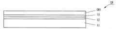
図1は、本実施形態の結晶CRの概略構成を示す図である。図1に示すように、結晶CRは、サファイア基板11と、バッファ層12と、GaN層13と、単結晶CR1と、を有する。単結晶CR1は、III 族窒化物半導体から成る単結晶である。単結晶CR1は、結晶CRからサファイア基板11等を除去することにより得られる。(First embodiment)
1. Semiconductor Single Crystal FIG. 1 is a diagram showing a schematic configuration of a crystal CR of this embodiment. As shown in FIG. 1, the crystalline CR has a
2.半導体結晶の製造装置
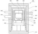
図2は、本実施形態の半導体単結晶の製造装置の全体像を示す概念図である。図2に示すように、製造装置A1は、結晶成長装置1000と、Na循環装置2000と、グローブボックス3000と、中継室RM1と、パスボックスPB1、PB2と、を有する。2. 2. Semiconductor Crystal Manufacturing Apparatus FIG. 2 is a conceptual diagram showing an overall image of a semiconductor single crystal manufacturing apparatus according to the present embodiment. As shown in FIG. 2, the manufacturing apparatus A1 has a
結晶成長装置1000は、種結晶の上にIII 族窒化物半導体を成長させるための結晶成長炉である。Na循環装置2000は、Na材料の純度を調整するための装置である。グローブボックス3000は、坩堝の内部にNa材料とGa材料とを収容する作業を実施するための装置である。中継室RM1は、坩堝を結晶成長装置1000に中継するためのものである。パスボックスPB1は、原料や坩堝などをグローブボックス3000に送るための装置である。パスボックスPB2は、坩堝をグローブボックス3000から中継室RM1に送るための装置である。 A
3.結晶成長装置
図3は、本実施形態の結晶CRを製造するための結晶成長装置1000である。結晶成長装置1000は、Naフラックス法を用いて成長基板上にIII 族窒化物半導体の単結晶を成長させるためのものである。3. Crystal Growth Apparatus FIG. 3 shows a
図3に示すように、結晶成長装置1000は、圧力容器1100と、圧力容器蓋1110と、中間室1200と、反応室1300と、反応室蓋1310と、回転軸1320と、ターンテーブル1330と、側部ヒーター1410と、下部ヒーター1420と、ガス供給口1510と、ガス排気口1520と、真空引き排気口1530と、測定用通気口1540と、Qmass取付口1550と、を有する。 As shown in FIG. 3, the
圧力容器1100は、結晶成長装置1000の筐体である。圧力容器蓋1110は、圧力容器1100の鉛直下方の位置に配置されている。中間室1200は、圧力容器1100の内部の室である。反応室1300は、坩堝CB1を収容し、その内部で半導体単結晶を成長させるための室である。反応室蓋1310は、反応室1300の蓋である。
回転軸1320は、正回転および負回転をすることができるようになっている。回転軸1320は、モーター(図示せず)から回転駆動を受けることができる。ターンテーブル1330は、回転軸1320に連れまわって回転することができる。側部ヒーター1410および下部ヒーター1420は、反応室1300を加熱するためのものである。 Rotating
ガス供給口1510は、圧力容器1100の内部に窒素ガスを含むガスを供給するための供給口である。ガス排気口1520は、圧力容器1100の内部からガスを排気するためのものである。真空引き排気口1530は、圧力容器1100を真空引きするためのものである。測定用通気口1540は、圧力容器1100の内部のガスを測定のために抽出するためのものである。測定用通気口1540のガスの流れの下流の位置には、O2 センサーや露点計が配置されている。Qmass取付口1550は、Qmass装置を取り付けるためのものである。 The
結晶成長装置1000は、坩堝CB1の内部の温度および圧力を調整するとともに坩堝CB1を回転させることができる。そのため、坩堝CB1の内部では、所望の条件で種結晶から半導体単結晶を成長させることができる。
4.Na循環装置
4-1.Na循環装置の構成
図4は、本実施形態の半導体単結晶の製造方法に用いられるNa循環装置2000を示す図である。Na循環装置2000は、Naを循環させつつNaの純度を制御する装置である。Na循環装置2000は、グローブボックス3000と連結されている。そのため、Na循環装置2000により純度を上げたNa材料をグローブボックス3000の内部に供給することができる。Na材料は露点および雰囲気を管理されたグローブボックス3000に供給される。そのため、グローブボックス3000に供給されるNa材料は、酸素や水分との反応を抑制されている。4. Na circulation device 4-1. Configuration of Na Circulating Device FIG. 4 is a diagram showing a
Na循環装置2000は、供給タンク2100と、ダンプタンク2200と、コールドトラップ2300と、電磁ポンプ2400と、膨張タンク2500と、計量タンク2600と、Na採取口2700と、配管2810、2820、2830と、を有する。また、Na循環装置2000は、その他の配管と、弁と、各部を加熱する加熱装置と、を有する。加熱装置は、各部の温度を設定した温度に保持することができる。 The
Na循環装置2000は、Na材料を液体状にして流す循環経路LP1を有する。循環経路LP1は、コールドトラップ2300と、膨張タンク2500と、電磁ポンプ2400と、配管2810、2820、2830と、を有する。 The
供給タンク2100は、初期のNa材料をNa循環装置2000に供給するためのタンクである。初期のNa材料は、ある程度高い純度のNa材料であるが、微量の不純物を含んでいる。初期のNa材料は固体である。供給タンク2100は加熱されているため、Na材料は液体になる。そして、液体状のNa材料は、ダンプタンク2200に送られる。 The
ダンプタンク2200は、反射衝撃波を吸収することのできるものである。 The
コールドトラップ2300は、Na材料中の不純物を除去するためのものである。コールドトラップ2300は、酸素等の不純物を除去または添加するNa純度制御部も兼ねている。コールドトラップ2300の詳細については後述する。 The
電磁ポンプ2400は、Na材料を膨張タンク2500からコールドトラップ2300に戻すためのものである。Na循環装置2000は、Na材料をコールドトラップ2300と膨張タンク2500との間で循環させることにより、Na材料を精製する。
膨張タンク2500は、コールドトラップ2300により不純物等を除去されたNa材料を一時的に貯蔵しておくためのNa貯蔵部である。 The
計量タンク2600は、Na採取口2700から取り出すNa材料の量を計量するためのものである。計量タンク2600に貯蔵されているNa材料の純度は十分に高い。 The weighing
Na採取口2700は、精製したNa材料をグローブボックス3000に供給するための供給口である。
4-2.Na循環装置の動作
このように、固体状のNa材料をNa循環装置2000の供給タンク2100に供給する。Na材料は、供給タンク2100により加熱され、液体状のNa材料となる。液体状のNa材料は、ダンプタンク2200に送られる。そして、液体状のNa材料は、ダンプタンク2200から循環経路LP1に徐々に送られる。液体状のNa材料は、循環経路LP1を循環することとなる。4-2. Operation of Na Circulator As described above, solid Na material is supplied to the
ここで、Na材料の温度が高いほど、Na中への酸素の溶解度は高い。コールドトラップ2300は、循環経路LP1のうちで最も温度の低い箇所である。そのため、コールドトラップ2300の箇所で例えばNa2 Oが析出する。Na2 Oについてはフィルター等により除去すればよい。 Here, the higher the temperature of the Na material, the higher the solubility of oxygen in Na.
液体状のNa材料は、循環経路LP1を循環する間に高温状態と低温状態との2つの状態を交互に繰り返すこととなる。このため、液体状のNa材料から酸素が繰り返し除去される。そして、純度の高いNa材料が精製される。Na採取口2700が供給するNa材料は液体である。液体状のNa材料はグローブボックス3000の内部の容器に注がれる。液体状のNa材料はその容器の中で冷却されて固体となる。 The liquid Na material alternately repeats two states, a high temperature state and a low temperature state, while circulating through the circulation path LP1. Therefore, oxygen is repeatedly removed from the liquid Na material. A highly pure Na material is then refined. The Na material supplied by the
4-3.コールドトラップの温度
コールドトラップ2300の温度は、120℃以上300℃以下である。膨張タンク2500およびその周囲の配管2810、2820、2830の温度は、コールドトラップ2300の温度より高い。このため、コールドトラップ2300によりNa材料中の不純物を除去することができる。そして、コールドトラップ2300の設定温度とNa材料中の酸素濃度との間には相関関係がある。そのため、コールドトラップ2300の温度を120℃以上300℃以下の範囲内で設定温度を選択することにより、Na材料中の酸素濃度等を制御することができる。4-3. Temperature of Cold Trap The temperature of the
5.グローブボックス
図5は、本実施形態の半導体素子の製造方法に用いられるグローブボックス3000を示す図である。グローブボックス3000は、Na材料等を処理するための処理室である。グローブボックス3000の内圧は、1気圧よりやや高い。グローブボックス3000の周囲の大気がグローブボックス3000の内部に入りにくくするためである。グローブボックス3000は、筐体3100と、グローブGL1と、窓WD1と、露点計3110と、Ar循環装置3200と、Ar供給管3310と、Ar排気管3320と、Ar通気口3321と、O2 センサーと、を有する。5. Glove Box FIG. 5 is a diagram showing a
筐体3100は、内部の雰囲気を所定の条件下に保持する。グローブGL1は、作業者がグローブボックス3000の内部のNa材料等を処理するためのものである。窓WD1は、作業者がグローブボックス3000の内部を視認するためのものである。露点計3110は、グローブボックス3000の内部の露点を測定する。 The
Ar循環装置3200は、Arガスの供給と回収とを行うための装置である。Ar供給管3310は、ArガスをAr循環装置3200からグローブボックス3000の内部に供給するためのものである。Ar排気管3320は、ArガスをAr循環装置3200に回収するためのものである。Ar排気管3320は、途中でAr通気口3321に分岐している。Ar通気口3321の下流の位置には、O2 センサーが配置されている。
このように、Ar循環装置3200が設けられているため、グローブボックス3000の内部は、Ar雰囲気である。グローブボックス3000の内部の酸素濃度は0.05ppm以下である。Ar通気口3321のO2 センサーが、グローブボックス3000の内部の酸素濃度を測定する。O2 センサーとして例えば、DF-150E(Servomex社製)が挙げられる。 Since the
グローブボックス3000の内部の水分濃度は0.05ppm以下である。水分濃度は、露点計3110により測定する。例えば、静電容量式露点計MMS35(GEセンシング&インスペクション・テクノロジーズ社製)を用いることができる。0.05ppmは、露点-94℃に相当する。 The moisture concentration inside the
6.不純物濃度(酸素取り込み量)
本実施形態では、製造装置A1により坩堝CB1に混入するであろう不純物濃度を制御しながら半導体単結晶を成長させる。主要な不純物として酸素および水分が挙げられる。結晶成長装置1000においては、酸素濃度および水素濃度が高い精度で制御されている。6. Impurity concentration (oxygen uptake)
In this embodiment, the semiconductor single crystal is grown while controlling the concentration of impurities that would be mixed in the crucible CB1 by the manufacturing apparatus A1. Major impurities include oxygen and moisture. In
7.グレイン
7-1.酸素取り込み量とグレインとの間の関係
ここで、Na材料への酸素取り込み量と成長初期に種結晶の上に形成されるグレインとの間の関係について説明する。7. Grain 7-1. Relationship Between Amount of Oxygen Uptake and Grains Here, the relationship between the amount of oxygen uptake into the Na material and the grains formed on the seed crystal in the early stage of growth will be described.
図6は、種結晶およびグレインを説明するための図(その1)である。図6に示すように、半導体結晶は、種結晶10とグレインGr1と半導体層Ep1とを有する。グレインGr1は、六角錐台形状または六角錐台形状に近い形状である。 FIG. 6 is a diagram (part 1) for explaining seed crystals and grains. As shown in FIG. 6, the semiconductor crystal has a
図7は、種結晶およびグレインを説明するための図(その2)である。図7に示すように、半導体結晶は、種結晶10とグレインGr2と半導体層Ep2とを有する。グレインGr2は、六角錐台形状または六角錐台形状に近い形状である。 FIG. 7 is a diagram (part 2) for explaining seed crystals and grains. As shown in FIG. 7, the semiconductor crystal has a
図6のグレインGr1は、図7のグレインGr2よりも大きい。ここで、融液への酸素取り込み量が少ない場合には、図6に示すように、グレインの大きさは大きい。融液への酸素取り込み量が多い場合には、図7に示すように、グレインの大きさは小さい。そして、グレインが大きいほど、その上に成長させた半導体結晶の応力は小さい。グレインから半導体結晶が成長して互いに合流する際の合流箇所が少なくなるからであると考えられる。グレインが大きいほど、半導体単結晶の反りは小さくなる傾向がある。 The grain Gr1 in FIG. 6 is larger than the grain Gr2 in FIG. Here, when the amount of oxygen taken into the melt is small, the size of the grains is large, as shown in FIG. When the amount of oxygen taken into the melt is large, the grain size is small, as shown in FIG. The larger the grain, the smaller the stress of the semiconductor crystal grown thereon. This is probably because the number of confluence points is reduced when the semiconductor crystals grow from the grains and merge with each other. The larger the grain, the smaller the warp of the semiconductor single crystal tends to be.
7-2.グレインサイズ
図8は、結晶CRの断面を示す断面図である。境界面Sf1におけるグレインGr1の平均幅W1が、10μm以上100μm以下であるとよい。グレインを観察するために、観測しようとする断面の手前(数μm~数十μm)まで研磨等により除去し、平坦化する。そしてその断面を蛍光顕微鏡やカソードルミネセンス装置により観察する。7-2. Grain Size FIG. 8 is a cross-sectional view showing a cross-section of a crystal CR. The average width W1 of the grains Gr1 at the boundary surface Sf1 is preferably 10 μm or more and 100 μm or less. In order to observe the grains, the cross section to be observed (several μm to several tens of μm) is removed by polishing or the like and flattened. Then, the cross section is observed with a fluorescence microscope or a cathodoluminescence device.
したがって、後述するように、Na材料から酸素原子を除去することにより、内部応力の小さい半導体結晶を成長させることができる。もちろん、半導体製造装置の内部やそこに至る過程で過大な酸素汚染がないように注意する必要がある。 Therefore, as will be described later, by removing oxygen atoms from the Na material, a semiconductor crystal with less internal stress can be grown. Of course, care must be taken to avoid excessive oxygen contamination inside the semiconductor manufacturing equipment and in the process leading there.
8.半導体単結晶の製造方法
この製造方法は、フラックス法によりIII 族窒化物半導体を成長させるIII 族窒化物半導体単結晶の製造方法である。この製造方法は、Na循環装置を用いてNa材料のNa純度を制御するNa純度制御工程と、坩堝の内部にNa材料とGa材料と種結晶とを入れて種結晶の上にIII 族窒化物半導体を成長させる半導体成長工程と、を有する。8. Semiconductor Single Crystal Manufacturing Method This manufacturing method is a group III nitride semiconductor single crystal manufacturing method in which a group III nitride semiconductor is grown by a flux method. This manufacturing method includes a Na purity control step of controlling the Na purity of the Na material using a Na circulation device, and a Na material, a Ga material, and a seed crystal placed inside a crucible, and a Group III nitride is deposited on the seed crystal. and a semiconductor growth step of growing a semiconductor.
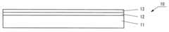
8-1.種結晶準備工程
まず、種結晶を準備する。図9は、種結晶10の概略構成を示す図である。図9に示すように、種結晶10は、サファイア基板11と、バッファ層12と、GaN層13と、を有する。種結晶10は、図1の単結晶CR1を成長させる前のテンプレート基板である。まず、サファイア基板11を用意する。そして、MOCVD法により、サファイア基板11のc面上に、バッファ層12を形成する。バッファ層12は、例えば、GaNである。また、TiNやAlNであってもよい。8-1. Seed Crystal Preparing Step First, seed crystals are prepared. FIG. 9 is a diagram showing a schematic configuration of
次に、バッファ層12の上に、GaN層13を形成する。これにより、種結晶10が製造される。これらのバッファ層12およびGaN層13は、シード層である。なお、GaN層13は、もちろん、GaNから成る層であるが、AlGaNやInGaN、AlInGaNであってもよい。このGaN層13は、成長条件によっては、フラックス中でメルトバックを起こす層である。その場合には、GaN層13の一部はフラックス中に溶解する。 Next, a
種結晶10については市場で購入してもよい。また、種結晶10として、マスクを形成したGaN基板、GaNを加工したGaN基板、GaNを選択的に除去したパターン基板等、その他の基板を用いてもよい。 The
8-2.Na純度制御工程
まず、Na循環装置2000によりNa材料を精製する。固体状のNa材料を加熱することにより、液体状のNaにする。液体状のNaにおいては、温度が高いほど酸素が溶け込む。8-2. Na Purity Control Step First, the Na material is purified by the
コールドトラップ2300の温度は120℃以上300℃以下である。膨張タンク2500の温度は、コールドトラップ2300の温度よりも高い。そのため、コールドトラップ2300の内部で、Na2 O等が析出する。そして、フィルター等を用いてNa2 O等の不純物を除去する。溶融状態のNa材料はコールドトラップ2300と膨張タンク2500とを循環する。そのため、Na2 O等の不純物が徐々に除去されていく。 The temperature of the
一方、グローブボックス3000の内部に坩堝CB1を準備する。その坩堝CB1の内部にGa等の材料を収容する。次に、Na循環装置2000が、Na純度を制御済みの溶融状態のNa材料をグローブボックスる3000の内部の坩堝CB1に、供給量を計量しながら注ぐ。このため、Gaは液体状のNa材料に浸される。 On the other hand, crucible CB1 is prepared inside
その後、液体状のNa材料の上に種結晶10を置く。このとき液状のNa材料は、坩堝CB1の底部および側壁に接するとともに種結晶10により蓋をされている状態にある。そのため、液状のNa材料が周囲の雰囲気と接する面積は非常に小さい。したがって、Na材料を坩堝CB1に注いだ後には液状のNa材料に不純物が入りにくい。なお、種結晶10の成長開始面は、液状のNa材料の反対側を向いている。 After that, the
8-3.半導体成長工程
次に、液相エピタキシー法の一種であるフラックス法を用いて、種結晶10上に半導体単結晶の層を成長させる。ここで用いる原材料の一例を表1に示す。また、炭素比を、0.1mol%以上2.0mol%以下の範囲内で変えてもよい。なお、表1の値は、あくまで例示であり、これ以外の値であってもよい。また、これ以外にドーピング元素を添加してもよい。8-3. Semiconductor Growth Step Next, a semiconductor single crystal layer is grown on the
ここで成長させる半導体単結晶は、もちろんIII 族窒化物半導体単結晶である。例えば、GaNである。なお、結晶成長装置1000を用いる前に事前にベークしておくとよい。結晶成長装置1000の内部の酸素および水分を極力減らすためである。 The semiconductor single crystal grown here is, of course, a Group III nitride semiconductor single crystal. For example, GaN. It should be noted that the
坩堝CB1を3重の育成容器に入れる。グローブボックス3000から反応室1300へ坩堝CB1を移動させる際に、Na材料が酸素および水分と反応することを抑制するためである。また、グローブボックス3000から反応室1300までの坩堝CB1の移動経路を窒素雰囲気にするとよい。Na材料の反応をさらに抑制できるからである。 Place the crucible CB1 in the triple growing vessel. This is to prevent the Na material from reacting with oxygen and moisture when moving the crucible CB1 from the
そして、その坩堝CB1を反応室1300のターンテーブル1330上に置く。この後、圧力容器1100を真空引きした後に昇圧および昇温する。そして、坩堝CB1を回転させつつ半導体単結晶を成長させる。なお、撹拌の方法、タイミングは任意である。そのため、撹拌することなく成長させてもよい。また、撹拌の有無について途中で変えてもよい。 Then, the crucible CB1 is placed on the
[表1]
原材料 原材料の量
Ga/Na比 10~40mol%
C 0.1mol%~2.0mol%(Naに対して)[Table 1]
Raw materials Amount of raw materials Ga/
C 0.1 mol% to 2.0 mol% (relative to Na)
ここで、この半導体単結晶形成工程で用いた坩堝内の各種条件を表2に示す。半導体単結晶の成長温度は、例えば870℃である。圧力は、例えば3MPaである。育成時間はおよそ20時間から200時間である。なお、結晶成長装置1000の内部の酸素濃度および水分濃度は、Qmass等により測定することができる。 Here, Table 2 shows various conditions in the crucible used in this semiconductor single crystal forming step. The growth temperature of a semiconductor single crystal is 870° C., for example. The pressure is, for example, 3 MPa. The growing time is approximately 20 to 200 hours. The oxygen concentration and water concentration inside the
[表2]
温度 700℃~900℃程度
圧力 2MPa~10MPa
攪拌速度 0rpm~100rpm
育成時間 20~200時間[Table 2]
Temperature about 700°C to 900°C Pressure 2MPa to 10MPa
Stirring speed 0rpm~100rpm
Growing time 20-200 hours
9.変形例
9-1.Na純度制御工程
Na純度制御工程において、コールドトラップ2300の温度を300℃近くに設定してもよい。その場合には、Na循環装置2000の周囲の雰囲気から、酸素がコールドトラップ2300に入る。そして、その酸素が溶融状態のNa材料に混入する。これにより、Na材料に含まれる酸素濃度を高めることができる。このように、Na純度制御工程では、コールドトラップ2300の温度を制御することにより、成長に用いるNa中の酸素濃度をコントロールすることができる。また、Na材料に含まれる酸素濃度を低くすること、またはNa材料に含まれる酸素濃度を高くすることもできる。9. Modification 9-1. Na Purity Control Step In the Na purity control step, the temperature of the
9-2.種結晶としての再利用
半導体成長工程で成長させたIII 族窒化物半導体を種結晶として用いてもよい。その場合には、得られたその種結晶の上にIII 族窒化物半導体を再成長させる。つまり、種結晶の上に半導体を成長させる第1の半導体成長工程と、第1の半導体成長工程で得られた半導体を種結晶にしてその種結晶の上に半導体を成長させる第2の半導体成長工程と、を有する。反りやオフ角分布が小さい種結晶を使うことにより従来より品質の良い半導体単結晶を厚く成長させることができる。9-2. Reuse as Seed Crystal Group III nitride semiconductors grown in a semiconductor growth process may be used as seed crystals. In that case, the group III nitride semiconductor is regrown on the obtained seed crystal. That is, a first semiconductor growth step for growing a semiconductor on a seed crystal, and a second semiconductor growth step for growing a semiconductor on the seed crystal using the semiconductor obtained in the first semiconductor growth step as a seed crystal. and By using a seed crystal with small warp and off-angle distribution, it is possible to grow a thicker semiconductor single crystal with better quality than conventional ones.
9-3.Na循環装置の構成
Na循環装置2000の構成については、図4と異なっていてもよい。9-3. Configuration of Na Circulator The configuration of the
9-4.組み合わせ
上記の変形例を自由に組み合わせてもよい。9-4. Combination The above modifications may be freely combined.
(第2の実施形態)
第1の実施形態では、III 族窒化物半導体の単結晶の製造方法について説明した。第2の実施形態では、そのIII 族窒化物半導体の単結晶を自立基板として用いた半導体素子について説明する。(Second embodiment)
In the first embodiment, a method for manufacturing a single crystal of a Group III nitride semiconductor has been described. In the second embodiment, a semiconductor device using the group III nitride semiconductor single crystal as a free-standing substrate will be described.
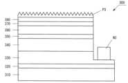
1.縦型構造の半導体素子
本実施形態に係るパワー素子100を図10に示す。パワー素子100は、縦型構造の半導体装置である。パワー素子100は、図10中の下側に示すように、ドレイン電極D1と、図10中の上側に示すように、ゲート電極G1と、ソース電極S1とを有している。1. Semiconductor Device with Vertical Structure FIG. 10 shows a
パワー素子100は、III 族窒化物半導体から成る複数の半導体層を有する。パワー素子100は、上記の電極の他に、図10に示すように、基板110と、n型層120と、p型層130と、n型層140と、絶縁膜150と、を有している。n型層120は、基板110の側から順に、n+ GaN層121と、n- GaN層122と、を有している。ソース電極S1は、n型層140とコンタクトしている。ドレイン電極D1は、基板110とコンタクトしている。The
2.自立基板の製造方法
基板110は、第1の実施形態の結晶CRから作製された自立基板である。ここで、自立基板とは、円板状のもの(ウエハ)の他、素子分離後のものも含むものとする。そのために、結晶CRからサファイア基板11等を取り外す。この取り外しには、レーザーリフトオフ法など、公知の技術を用いてもよい。そして、単結晶CR1の両面を研磨等の加工をすることにより、基板110が得られる。また、この基板110に、凹凸形状等を形成することとしてもよい。また、両面を研磨したものでなくとも、両面のうちの少なくとも一方の面を研磨したものであってもよい。また、基板110は、結晶成長工程の後の冷却中の熱ひずみを利用して剥離させたものであってもよい。2. Manufacturing Method of Freestanding Substrate The
3.半導体素子の製造方法
MOCVD法等により、上記の自立基板の上にIII 族窒化物半導体の各層を成長させる。次に、エッチング技術を用いて半導体にトレンチを形成する。また、半導体に絶縁膜および電極を形成する。そして、各チップに分割する。3. Manufacturing Method of Semiconductor Device Each layer of the group III nitride semiconductor is grown on the self-supporting substrate by the MOCVD method or the like. An etching technique is then used to form trenches in the semiconductor. Also, an insulating film and an electrode are formed on the semiconductor. Then, it is divided into each chip.
4.変形例
4-1.横型構造の半導体装置
本実施形態の半導体装置は、縦型構造の半導体装置である。しかし、本実施形態の自立基板を、図11に示すような横型構造の半導体装置200について適用してもよい。図11の半導体装置200は、HFETである。半導体装置200は、基板210と、バッファ層220と、第1キャリア走行層230と、第2キャリア走行層240と、キャリア供給層250と、絶縁膜260と、ドレイン電極D2と、ソース電極S2と、ゲート電極G2と、を有している。ここで、基板210は、単結晶CR1を加工したものである。4. Modification 4-1. Semiconductor Device with Horizontal Structure The semiconductor device of this embodiment is a semiconductor device with a vertical structure. However, the self-supporting substrate of the present embodiment may be applied to a
4-2.半導体発光素子
また、図12に示すような半導体発光素子300について適用してもよい。以上説明したように、第1の実施形態の製造方法により得られた単結晶CR1を種々の半導体装置に適用することができる。半導体発光素子300は、基板310と、半導体層と、p電極P3と、n電極N3と、を有している。ここで、基板310は、単結晶CR1を加工したものである。4-2. Semiconductor Light Emitting Device Further, it may be applied to a semiconductor
半導体層は、基板310の主面の上から、バッファ層320と、n型コンタクト層330と、n型静電耐圧層340と、n型クラッド層350と、発光層360と、p型クラッド層370と、p型コンタクト層380とを、この順序で配置されるように形成されたものである。p電極P3は、p型コンタクト層380と接触している。n電極N3は、n型コンタクト層330と接触している。 The semiconductor layers are, from above the main surface of the
(実験)
1.実験方法
製造装置A1を用いてGaN単結晶を製造した。種結晶は、サファイア基板の上にGaN層を形成したものである。コールドトラップ2300の温度を変えて、反りの発生量または雑晶の発生量との間の関係を調べた。なお、膨張タンク2500の温度は400℃であった。(experiment)
1. Experimental method A GaN single crystal was manufactured using the manufacturing apparatus A1. A seed crystal is obtained by forming a GaN layer on a sapphire substrate. By changing the temperature of the
2.実験結果
図13は、コールドトラップ2300の温度と反りと雑晶との間の関係を示すグラフである。図13の横軸はコールドトラップの温度である。図13の縦軸は反りまたは雑晶の発生量である。反りは、曲率半径の逆数(1/m)で表される。雑晶の発生量は、雑晶の重さ(g)である。2. Experimental Results FIG. 13 is a graph showing the relationship between the temperature of the
図13に示すように、コールドトラップ2300の温度が高いほど、反りは大きく、雑晶の重量は小さくなる。つまり、反りを考慮すると、コールドトラップ2300の温度は低いほうがよく、雑晶の発生量を考慮すると、コールドトラップ2300の温度は高いほうがよい。つまり、反りの大きさと雑晶の発生量とはトレードオフの関係にある。 As shown in FIG. 13, the higher the temperature of the
コールドトラップ2300の温度が120℃以上300℃以下の場合(図13の領域R1)には、半導体の反りと雑晶の発生量との少なくとも一方が抑制されている。領域R1では、反りがおよそ0.4/m以下であり、雑晶の発生量がおよそ8g以下である。 When the temperature of the
コールドトラップ2300の温度が120℃以上230℃以下の場合(図13の領域R2)には、反りはおよそ0.3/m以下である。このように、半導体の反りが抑制されている。 When the temperature of the
コールドトラップ2300の温度が180℃以上300℃以下の場合(図13の領域R3)には、雑晶の発生量はおよそ2g以下である。このように、雑晶の発生量が抑制されている。 When the temperature of the
コールドトラップ2300の温度が180℃以上230℃以下の場合(図13の領域R4)には、半導体の反りが0.3/m以下であるとともに、雑晶の発生量が2g以下である。このように、半導体の反りおよび雑晶の発生量が抑制されている。 When the temperature of the
半導体の反りが小さいほど、半導体中の転位密度が減少する傾向がある。そのため、半導体の反りが小さいほど、半導体の結晶性はよい。また、反りの小さい結晶ほど加工により平坦化させやすく、ウエハのオフ角分布を小さくできる。ただし、半導体の反りがある程度あると、種結晶から半導体単結晶を取り外しやすい。 The dislocation density in the semiconductor tends to decrease as the warp of the semiconductor decreases. Therefore, the smaller the warpage of the semiconductor, the better the crystallinity of the semiconductor. Also, a crystal with a smaller warp is easier to flatten by processing, and the off-angle distribution of the wafer can be reduced. However, if the semiconductor warps to some extent, it is easy to remove the semiconductor single crystal from the seed crystal.
なお、雑晶が多いと、III 族窒化物半導体の結晶性が悪くなるおそれがある。つまり、III 族窒化物半導体の歩留りが低下するおそれがある。そのため、一般に、雑晶の発生量は少なければ少ないほどよい。しかし、所望の品質の半導体結晶を得るために、あえて雑晶が発生する条件を選択することも可能である。 If there are many miscellaneous crystals, the crystallinity of the group III nitride semiconductor may deteriorate. In other words, there is a possibility that the yield of group III nitride semiconductors is lowered. Therefore, in general, the smaller the amount of miscellaneous crystals, the better. However, in order to obtain a semiconductor crystal of desired quality, it is also possible to deliberately select conditions under which miscellaneous crystals are generated.
(付記)
第1の態様におけるIII 族窒化物半導体単結晶の製造方法は、フラックス法によりIII 族窒化物半導体を成長させるIII 族窒化物半導体単結晶の製造方法である。この製造方法は、Na循環装置を用いてNa材料のNa純度を制御するNa純度制御工程と、坩堝の内部にNa材料とGa材料と種結晶とを入れて種結晶の上にIII 族窒化物半導体を成長させる半導体成長工程と、を有する。Na循環装置は、Na材料を液体状にして流す循環経路を有する。循環経路は、Na純度制御部と、配管と、を有する。Na純度制御工程では、Na純度制御部の温度を120℃以上300℃以下とする。(Appendix)
A method for producing a Group III nitride semiconductor single crystal according to a first aspect is a method for producing a Group III nitride semiconductor single crystal in which a Group III nitride semiconductor is grown by a flux method. This manufacturing method includes a Na purity control step of controlling the Na purity of the Na material using a Na circulation device, and a Na material, a Ga material, and a seed crystal placed inside a crucible, and a Group III nitride is deposited on the seed crystal. and a semiconductor growth step of growing a semiconductor. The Na circulation device has a circulation path for flowing the Na material in a liquid state. The circulation path has a Na purity control section and piping. In the Na purity control step, the temperature of the Na purity control unit is set at 120°C or higher and 300°C or lower.
第2の態様におけるIII 族窒化物半導体単結晶の製造方法においては、Na循環経路は、Na貯蔵部を有する。Na貯蔵部および配管の温度は、Na純度制御部の温度より高い。 In the method for producing a Group III nitride semiconductor single crystal according to the second aspect, the Na circulation path has a Na reservoir. The temperature of the Na storage section and piping is higher than the temperature of the Na purity control section.
第3の態様におけるIII 族窒化物半導体単結晶の製造方法においては、Na純度制御工程の後に、Na循環装置から液体状のNa材料を計量しつつ保持室の内部の容器に注ぐ。 In the method for producing a group III nitride semiconductor single crystal according to the third aspect, after the Na purity control step, the liquid Na material is measured and poured from the Na circulation device into the container inside the holding chamber.
第4の態様におけるIII 族窒化物半導体単結晶の製造方法においては、半導体成長工程で成長させたIII 族窒化物半導体を種結晶として用い、その種結晶の上にIII 族窒化物半導体を再成長させる。 In the method for producing a group III nitride semiconductor single crystal according to the fourth aspect, the group III nitride semiconductor grown in the semiconductor growth step is used as a seed crystal, and the group III nitride semiconductor is regrown on the seed crystal. Let
第5の態様におけるIII 族窒化物半導体素子の製造方法は、フラックス法によりIII 族窒化物半導体を成長させるIII 族窒化物半導体素子の製造方法である。この製造方法は、Na循環装置を用いてNa材料のNa純度を制御するNa純度制御工程と、坩堝の内部にNa材料とGa材料と種結晶とを入れて種結晶の上にIII 族窒化物半導体を成長させる半導体成長工程と、を有する。Na循環装置は、Na材料を液体状にして流す循環経路を有する。循環経路は、Na純度制御部と、配管と、を有する。Na純度制御工程では、Na純度制御部の温度を120℃以上300℃以下とする。 A method for manufacturing a group III nitride semiconductor device according to a fifth aspect is a method for manufacturing a group III nitride semiconductor device in which a group III nitride semiconductor is grown by a flux method. This manufacturing method includes a Na purity control step of controlling the Na purity of the Na material using a Na circulation device, and a Na material, a Ga material, and a seed crystal placed inside a crucible, and a Group III nitride is deposited on the seed crystal. and a semiconductor growth step of growing a semiconductor. The Na circulation device has a circulation path for flowing the Na material in a liquid state. The circulation path has a Na purity control section and piping. In the Na purity control step, the temperature of the Na purity control unit is set at 120°C or higher and 300°C or lower.
第6の態様におけるIII 族窒化物半導体素子の製造方法においては、Na純度制御工程の後に、Na循環装置から液体状のNa材料を計量しつつ保持室の内部の容器に注ぐ。 In the method for manufacturing a Group III nitride semiconductor device according to the sixth aspect, after the Na purity control step, the liquid Na material is measured and poured from the Na circulation device into the container inside the holding chamber.
CR…結晶
CR1…単結晶
10…テンプレート
11…サファイア基板
12…バッファ層
13…GaN層
GB…グローブボックス
100…パワー素子
200…半導体装置
300…半導体発光素子
1000…結晶成長装置
2000…Na循環装置CR...Crystal CR1...
Claims (3)
Translated fromJapanese前記炉の外部において、前記フラックスであるNaに含まれる酸素の濃度を制御して、その酸素濃度の制御されたNaを前記炉内に供給し、
前記酸素濃度により前記基板上に成長するIII 族窒化物半導体の反り又は雑晶の発生を制御する方法であって、
前記Naを液化させたNa融液を、第1温度に保持した第1状態と前記第1温度よりも低い120℃以上230℃以下の範囲の値の第2温度に保持した第2状態とを循環させて、前記第2状態のNa融液の酸化Naを除去し、前記第2温度の制御により前記Naに含まれる前記酸素濃度を制御することにより、
単位曲率半径当たりの反り量は、0.3/m以下に制御される
ことを特徴とするIII 族窒化物半導体の製造方法。In a method for producing a group III nitride semiconductor, a group III nitride semiconductor is grown on a seed substrate by supplying a nitrogen-containing gas to a molten mixture of a group III metal and a flux into a furnace, comprising:
outside the furnace, controlling the concentration of oxygen contained in Na, which is the flux, and supplying Na with the controlled oxygen concentration into the furnace;
A method for controlling warpage or generation of miscellaneous crystals in a group III nitride semiconductor grown on a substrate by means of the oxygen concentration, comprising:
A first state in which the Na melt obtained by liquefying the Na is held at a first temperature and a second state in which the Na melt is held at a second temperature in the range of 120° C. or more and 230° C. or less lower than the first temperature. By circulating to remove Na oxide from the Na melt in the second state and controlling the oxygen concentration contained in the Na by controlling the second temperature,
The amount of warpage per unit radius of curvature is controlled to 0.3/m or less
A method for producing a Group III nitride semiconductor, characterized by:
前記炉の外部において、前記フラックスであるNaに含まれる酸素の濃度を制御して、その酸素濃度の制御されたNaを前記炉内に供給し、
前記酸素濃度により前記基板上に成長するIII 族窒化物半導体の反り又は雑晶の発生を制御する方法であって、
前記Naを液化させたNa融液を、第1温度に保持した第1状態と前記第1温度よりも低い180℃以上300℃以下の範囲の値の第2温度に保持した第2状態とを循環させて、前記第2状態のNa融液の酸化Naを除去し、前記第2温度の制御により前記Naに含まれる前記酸素濃度を制御することにより、
雑晶の発生量は2g以下に制御される
ことを特徴とするIII 族窒化物半導体の製造方法。In a method for producing a group III nitride semiconductor, a group III nitride semiconductor is grown on a seed substrate by supplying a nitrogen-containing gas to a molten mixture of a group III metal and a flux into a furnace, comprising:
outside the furnace, controlling the concentration of oxygen contained in Na, which is the flux, and supplying Na with the controlled oxygen concentration into the furnace;
A methodfor controlling warpage or generation of miscellaneous crystals in a group III nitride semiconductor grown on a substrate by means of the oxygen concentration, comprising:
A first state in which the Na melt obtained by liquefying the Na is held at a first temperature and a second state in which the Na melt is held at a second temperature in the range of 180° C. or more and 300° C. or less lower than the first temperature. By circulating to remove Na oxide from the Na melt in the second state and controlling the oxygen concentration contained in the Na by controlling the second temperature,
The amount of miscellaneous crystals generated is controlled to 2g or less
A method for producing a Group III nitride semiconductor, characterized by:
前記循環経路は、Na貯蔵部と、前記第2温度に設定されるNa純度制御部と、配管と、を有し、
前記Na貯蔵部および前記配管の温度は、前記Na純度制御部の温度より高い
ことを特徴とする請求項1または請求項2に記載のIII 族窒化物半導体の製造方法。The circulation of the Na melt for controlling the oxygen concentration is performed using a Na circulation device having a circulation path for flowing the Na material in a liquid state,
The circulation path has a Na storage unit, a Na purity control unit set to the second temperature, and a pipe,
3. The method for producing a Group III nitride semiconductor according toclaim 1, wherein temperatures of the Na storage section and the pipe are higher than the temperature of the Na purity control section.
Priority Applications (5)
| Application Number | Priority Date | Filing Date | Title |
|---|---|---|---|
| JP2019069511AJP7226026B2 (en) | 2019-03-30 | 2019-03-30 | Group III nitride semiconductor device manufacturing method and Group III nitride semiconductor single crystal manufacturing method |
| US16/814,758US11280024B2 (en) | 2019-03-18 | 2020-03-10 | Method for producing a group III nitride semiconductor by controlling the oxygen concentration of the furnace internal atmosphere |
| US17/531,982US20220081800A1 (en) | 2019-03-18 | 2021-11-22 | Method for producing a group iii nitride semiconductor |
| JP2022180732AJP7501595B2 (en) | 2019-03-30 | 2022-11-11 | Method for manufacturing group III nitride semiconductor device and method for manufacturing group III nitride semiconductor single crystal |
| US18/123,598US20230257902A1 (en) | 2019-03-16 | 2023-03-20 | Method for producing a group iii nitride semiconductor |
Applications Claiming Priority (1)
| Application Number | Priority Date | Filing Date | Title |
|---|---|---|---|
| JP2019069511AJP7226026B2 (en) | 2019-03-30 | 2019-03-30 | Group III nitride semiconductor device manufacturing method and Group III nitride semiconductor single crystal manufacturing method |
Related Child Applications (1)
| Application Number | Title | Priority Date | Filing Date |
|---|---|---|---|
| JP2022180732ADivisionJP7501595B2 (en) | 2019-03-30 | 2022-11-11 | Method for manufacturing group III nitride semiconductor device and method for manufacturing group III nitride semiconductor single crystal |
Publications (2)
| Publication Number | Publication Date |
|---|---|
| JP2020164395A JP2020164395A (en) | 2020-10-08 |
| JP7226026B2true JP7226026B2 (en) | 2023-02-21 |
Family
ID=72715760
Family Applications (2)
| Application Number | Title | Priority Date | Filing Date |
|---|---|---|---|
| JP2019069511AActiveJP7226026B2 (en) | 2019-03-16 | 2019-03-30 | Group III nitride semiconductor device manufacturing method and Group III nitride semiconductor single crystal manufacturing method |
| JP2022180732AActiveJP7501595B2 (en) | 2019-03-30 | 2022-11-11 | Method for manufacturing group III nitride semiconductor device and method for manufacturing group III nitride semiconductor single crystal |
Family Applications After (1)
| Application Number | Title | Priority Date | Filing Date |
|---|---|---|---|
| JP2022180732AActiveJP7501595B2 (en) | 2019-03-30 | 2022-11-11 | Method for manufacturing group III nitride semiconductor device and method for manufacturing group III nitride semiconductor single crystal |
Country Status (1)
| Country | Link |
|---|---|
| JP (2) | JP7226026B2 (en) |
Citations (5)
| Publication number | Priority date | Publication date | Assignee | Title |
|---|---|---|---|---|
| JP2008254999A (en) | 2007-03-13 | 2008-10-23 | Toyoda Gosei Co Ltd | Crystal growth equipment |
| JP2008297153A (en) | 2007-05-30 | 2008-12-11 | Toyoda Gosei Co Ltd | Apparatus and method for producing group iii nitride semiconductor |
| JP2010189270A (en) | 2006-11-14 | 2010-09-02 | Osaka Univ | METHOD FOR PRODUCING GaN CRYSTAL, GaN CRYSTAL, GaN CRYSTAL SUBSTRATE, SEMICONDUCTOR DEVICE AND APPARATUS FOR PRODUCING GaN CRYSTAL |
| JP2012072047A (en) | 2010-08-31 | 2012-04-12 | Ricoh Co Ltd | Method for producing n-type group iii nitride single crystal, n-type group iii nitride single crystal, and crystal substrate |
| JP2013112550A (en) | 2011-11-28 | 2013-06-10 | Ihi Corp | Apparatus and method for supplying sodium |
Family Cites Families (1)
| Publication number | Priority date | Publication date | Assignee | Title |
|---|---|---|---|---|
| JP5003642B2 (en) | 2008-09-30 | 2012-08-15 | 豊田合成株式会社 | Group III nitride semiconductor crystal manufacturing equipment |
- 2019
- 2019-03-30JPJP2019069511Apatent/JP7226026B2/enactiveActive
- 2022
- 2022-11-11JPJP2022180732Apatent/JP7501595B2/enactiveActive
Patent Citations (5)
| Publication number | Priority date | Publication date | Assignee | Title |
|---|---|---|---|---|
| JP2010189270A (en) | 2006-11-14 | 2010-09-02 | Osaka Univ | METHOD FOR PRODUCING GaN CRYSTAL, GaN CRYSTAL, GaN CRYSTAL SUBSTRATE, SEMICONDUCTOR DEVICE AND APPARATUS FOR PRODUCING GaN CRYSTAL |
| JP2008254999A (en) | 2007-03-13 | 2008-10-23 | Toyoda Gosei Co Ltd | Crystal growth equipment |
| JP2008297153A (en) | 2007-05-30 | 2008-12-11 | Toyoda Gosei Co Ltd | Apparatus and method for producing group iii nitride semiconductor |
| JP2012072047A (en) | 2010-08-31 | 2012-04-12 | Ricoh Co Ltd | Method for producing n-type group iii nitride single crystal, n-type group iii nitride single crystal, and crystal substrate |
| JP2013112550A (en) | 2011-11-28 | 2013-06-10 | Ihi Corp | Apparatus and method for supplying sodium |
Also Published As
| Publication number | Publication date |
|---|---|
| JP2020164395A (en) | 2020-10-08 |
| JP2023001346A (en) | 2023-01-04 |
| JP7501595B2 (en) | 2024-06-18 |
Similar Documents
| Publication | Publication Date | Title |
|---|---|---|
| US7524376B2 (en) | Method and apparatus for aluminum nitride monocrystal boule growth | |
| JP4647525B2 (en) | Method for producing group III nitride crystal | |
| JP5788433B2 (en) | Process for large-scale ammonothermal production of semipolar gallium nitride boule | |
| TWI429797B (en) | Group III nitride semiconductor crystal substrate and semiconductor device | |
| US8764903B2 (en) | Growth reactor for gallium-nitride crystals using ammonia and hydrogen chloride | |
| JP2009126723A (en) | Group III nitride semiconductor crystal growth method, group III nitride semiconductor crystal substrate manufacturing method, and group III nitride semiconductor crystal substrate | |
| CN101925695A (en) | Group III nitride single crystal ingot, group III nitride single crystal substrate, method for manufacturing group III nitride single crystal ingot, and method for manufacturing group III nitride single crystal substrate | |
| JP5754191B2 (en) | Method for producing group 13 nitride crystal and method for producing group 13 nitride crystal substrate | |
| Kangawa et al. | Novel solution growth method of bulk AlN using Al and Li3N solid sources | |
| JP2018186252A (en) | Epitaxial growth apparatus and epitaxial growth method | |
| US20130052838A1 (en) | Annealing method to reduce defects of epitaxial films and epitaxial films formed therewith | |
| JP2009062231A (en) | Crystal growth method, crystal growth apparatus, stacked crystal growth apparatus, and semiconductor device having crystal thin film manufactured by these. | |
| JP7226026B2 (en) | Group III nitride semiconductor device manufacturing method and Group III nitride semiconductor single crystal manufacturing method | |
| JP7147644B2 (en) | Method for manufacturing group III nitride semiconductor | |
| US11441237B2 (en) | RAMO4 substrate and method of manufacture thereof, and group III nitride semiconductor | |
| JP7147664B2 (en) | Group III nitride semiconductor device manufacturing method and Group III nitride semiconductor single crystal manufacturing method | |
| JP5454558B2 (en) | Crystal manufacturing method | |
| TWI793167B (en) | Gallium Arsenide Compound Semiconductor Crystal and Wafer Group | |
| CN102640261B (en) | Manufacturing method of epitaxial silicon chip | |
| TW201204881A (en) | Process for producing single-crystal sapphire, and single-crystal sapphire substrate | |
| JP4908467B2 (en) | Method for producing group III nitride compound semiconductor crystal | |
| US20230257902A1 (en) | Method for producing a group iii nitride semiconductor | |
| JP5651480B2 (en) | Method for producing group 3B nitride crystals | |
| JP2017214232A (en) | Method of manufacturing nitride compound semiconductor substrate | |
| JP5491300B2 (en) | Aluminum nitride manufacturing method |
Legal Events
| Date | Code | Title | Description |
|---|---|---|---|
| A621 | Written request for application examination | Free format text:JAPANESE INTERMEDIATE CODE: A621 Effective date:20210528 | |
| A977 | Report on retrieval | Free format text:JAPANESE INTERMEDIATE CODE: A971007 Effective date:20220311 | |
| A131 | Notification of reasons for refusal | Free format text:JAPANESE INTERMEDIATE CODE: A131 Effective date:20220405 | |
| A521 | Request for written amendment filed | Free format text:JAPANESE INTERMEDIATE CODE: A523 Effective date:20220530 | |
| RD02 | Notification of acceptance of power of attorney | Free format text:JAPANESE INTERMEDIATE CODE: A7422 Effective date:20220701 | |
| A02 | Decision of refusal | Free format text:JAPANESE INTERMEDIATE CODE: A02 Effective date:20220823 | |
| A521 | Request for written amendment filed | Free format text:JAPANESE INTERMEDIATE CODE: A821 Effective date:20221111 Free format text:JAPANESE INTERMEDIATE CODE: A523 Effective date:20221111 | |
| C60 | Trial request (containing other claim documents, opposition documents) | Free format text:JAPANESE INTERMEDIATE CODE: C60 Effective date:20221111 | |
| A911 | Transfer to examiner for re-examination before appeal (zenchi) | Free format text:JAPANESE INTERMEDIATE CODE: A911 Effective date:20221118 | |
| C21 | Notice of transfer of a case for reconsideration by examiners before appeal proceedings | Free format text:JAPANESE INTERMEDIATE CODE: C21 Effective date:20221122 | |
| TRDD | Decision of grant or rejection written | ||
| A01 | Written decision to grant a patent or to grant a registration (utility model) | Free format text:JAPANESE INTERMEDIATE CODE: A01 Effective date:20230110 | |
| A61 | First payment of annual fees (during grant procedure) | Free format text:JAPANESE INTERMEDIATE CODE: A61 Effective date:20230123 | |
| R151 | Written notification of patent or utility model registration | Ref document number:7226026 Country of ref document:JP Free format text:JAPANESE INTERMEDIATE CODE: R151 |