JP7220626B2 - Plasma processing method and plasma processing apparatus - Google Patents
Plasma processing method and plasma processing apparatusDownload PDFInfo
- Publication number
- JP7220626B2 JP7220626B2JP2019112618AJP2019112618AJP7220626B2JP 7220626 B2JP7220626 B2JP 7220626B2JP 2019112618 AJP2019112618 AJP 2019112618AJP 2019112618 AJP2019112618 AJP 2019112618AJP 7220626 B2JP7220626 B2JP 7220626B2
- Authority
- JP
- Japan
- Prior art keywords
- power supply
- gas
- plasma
- plasma processing
- chamber
- Prior art date
- Legal status (The legal status is an assumption and is not a legal conclusion. Google has not performed a legal analysis and makes no representation as to the accuracy of the status listed.)
- Active
Links
- 238000012545processingMethods0.000titleclaimsdescription63
- 238000003672processing methodMethods0.000titleclaimsdescription27
- 230000001681protective effectEffects0.000claimsdescription69
- 239000000758substrateSubstances0.000claimsdescription51
- 238000000034methodMethods0.000claimsdescription32
- 229910052710siliconInorganic materials0.000claimsdescription22
- 239000010703siliconSubstances0.000claimsdescription22
- 238000000151depositionMethods0.000claimsdescription18
- XUIMIQQOPSSXEZ-UHFFFAOYSA-NSiliconChemical compound[Si]XUIMIQQOPSSXEZ-UHFFFAOYSA-N0.000claimsdescription14
- 230000008021depositionEffects0.000claimsdescription13
- 238000004140cleaningMethods0.000claimsdescription12
- OKTJSMMVPCPJKN-UHFFFAOYSA-NCarbonChemical compound[C]OKTJSMMVPCPJKN-UHFFFAOYSA-N0.000claimsdescription10
- 229910052799carbonInorganic materials0.000claimsdescription10
- -1silicon halideChemical class0.000claimsdescription8
- 239000013626chemical specieSubstances0.000claimsdescription6
- VXEGSRKPIUDPQT-UHFFFAOYSA-N4-[4-(4-methoxyphenyl)piperazin-1-yl]anilineChemical compoundC1=CC(OC)=CC=C1N1CCN(C=2C=CC(N)=CC=2)CC1VXEGSRKPIUDPQT-UHFFFAOYSA-N0.000claimsdescription5
- NBVXSUQYWXRMNV-UHFFFAOYSA-NfluoromethaneChemical compoundFCNBVXSUQYWXRMNV-UHFFFAOYSA-N0.000claimsdescription5
- 238000009832plasma treatmentMethods0.000claimsdescription5
- 239000005049silicon tetrachlorideSubstances0.000claimsdescription5
- 239000004215Carbon black (E152)Substances0.000claimsdescription4
- 229930195733hydrocarbonNatural products0.000claimsdescription4
- 150000002430hydrocarbonsChemical class0.000claimsdescription4
- 239000007789gasSubstances0.000description123
- 238000002474experimental methodMethods0.000description7
- XAGFODPZIPBFFR-UHFFFAOYSA-NaluminiumChemical compound[Al]XAGFODPZIPBFFR-UHFFFAOYSA-N0.000description6
- 229910052782aluminiumInorganic materials0.000description6
- 238000005260corrosionMethods0.000description6
- 230000007797corrosionEffects0.000description6
- 239000012528membraneSubstances0.000description6
- 230000015572biosynthetic processEffects0.000description5
- 238000010586diagramMethods0.000description5
- XKRFYHLGVUSROY-UHFFFAOYSA-NArgonChemical compound[Ar]XKRFYHLGVUSROY-UHFFFAOYSA-N0.000description4
- 239000004020conductorSubstances0.000description4
- 150000002500ionsChemical class0.000description4
- 239000002994raw materialSubstances0.000description4
- MYMOFIZGZYHOMD-UHFFFAOYSA-NDioxygenChemical compoundO=OMYMOFIZGZYHOMD-UHFFFAOYSA-N0.000description3
- 239000000919ceramicSubstances0.000description3
- 238000009792diffusion processMethods0.000description3
- 229910001882dioxygenInorganic materials0.000description3
- 239000000463materialSubstances0.000description3
- SIWVEOZUMHYXCS-UHFFFAOYSA-Noxo(oxoyttriooxy)yttriumChemical compoundO=[Y]O[Y]=OSIWVEOZUMHYXCS-UHFFFAOYSA-N0.000description3
- 239000000047productSubstances0.000description3
- VYPSYNLAJGMNEJ-UHFFFAOYSA-Nsilicon dioxideInorganic materialsO=[Si]=OVYPSYNLAJGMNEJ-UHFFFAOYSA-N0.000description3
- 238000012546transferMethods0.000description3
- 229910052786argonInorganic materials0.000description2
- 239000011810insulating materialSubstances0.000description2
- HBMJWWWQQXIZIP-UHFFFAOYSA-Nsilicon carbideChemical compound[Si+]#[C-]HBMJWWWQQXIZIP-UHFFFAOYSA-N0.000description2
- 229910010271silicon carbideInorganic materials0.000description2
- 229910052814silicon oxideInorganic materials0.000description2
- QVGXLLKOCUKJST-UHFFFAOYSA-Natomic oxygenChemical compound[O]QVGXLLKOCUKJST-UHFFFAOYSA-N0.000description1
- 239000006227byproductSubstances0.000description1
- 230000007423decreaseEffects0.000description1
- 230000003247decreasing effectEffects0.000description1
- 239000003989dielectric materialSubstances0.000description1
- 238000012986modificationMethods0.000description1
- 230000004048modificationEffects0.000description1
- 229910052756noble gasInorganic materials0.000description1
- 150000002835noble gasesChemical class0.000description1
- TWNQGVIAIRXVLR-UHFFFAOYSA-Noxo(oxoalumanyloxy)alumaneChemical compoundO=[Al]O[Al]=OTWNQGVIAIRXVLR-UHFFFAOYSA-N0.000description1
- 239000001301oxygenSubstances0.000description1
- 229910052760oxygenInorganic materials0.000description1
- 238000001020plasma etchingMethods0.000description1
- 239000011241protective layerSubstances0.000description1
- 239000010453quartzSubstances0.000description1
- 239000003507refrigerantSubstances0.000description1
- 230000001105regulatory effectEffects0.000description1
- 238000006467substitution reactionMethods0.000description1
Images


Classifications
- H—ELECTRICITY
- H01—ELECTRIC ELEMENTS
- H01J—ELECTRIC DISCHARGE TUBES OR DISCHARGE LAMPS
- H01J37/00—Discharge tubes with provision for introducing objects or material to be exposed to the discharge, e.g. for the purpose of examination or processing thereof
- H01J37/32—Gas-filled discharge tubes
- H01J37/32431—Constructional details of the reactor
- H01J37/3244—Gas supply means
- H—ELECTRICITY
- H01—ELECTRIC ELEMENTS
- H01J—ELECTRIC DISCHARGE TUBES OR DISCHARGE LAMPS
- H01J37/00—Discharge tubes with provision for introducing objects or material to be exposed to the discharge, e.g. for the purpose of examination or processing thereof
- H01J37/32—Gas-filled discharge tubes
- H01J37/32431—Constructional details of the reactor
- H01J37/32458—Vessel
- H01J37/32477—Vessel characterised by the means for protecting vessels or internal parts, e.g. coatings
- H—ELECTRICITY
- H01—ELECTRIC ELEMENTS
- H01L—SEMICONDUCTOR DEVICES NOT COVERED BY CLASS H10
- H01L21/00—Processes or apparatus adapted for the manufacture or treatment of semiconductor or solid state devices or of parts thereof
- H01L21/02—Manufacture or treatment of semiconductor devices or of parts thereof
- H01L21/04—Manufacture or treatment of semiconductor devices or of parts thereof the devices having potential barriers, e.g. a PN junction, depletion layer or carrier concentration layer
- H01L21/18—Manufacture or treatment of semiconductor devices or of parts thereof the devices having potential barriers, e.g. a PN junction, depletion layer or carrier concentration layer the devices having semiconductor bodies comprising elements of Group IV of the Periodic Table or AIIIBV compounds with or without impurities, e.g. doping materials
- H01L21/30—Treatment of semiconductor bodies using processes or apparatus not provided for in groups H01L21/20 - H01L21/26
- H01L21/302—Treatment of semiconductor bodies using processes or apparatus not provided for in groups H01L21/20 - H01L21/26 to change their surface-physical characteristics or shape, e.g. etching, polishing, cutting
- H01L21/306—Chemical or electrical treatment, e.g. electrolytic etching
- H01L21/3065—Plasma etching; Reactive-ion etching
- C—CHEMISTRY; METALLURGY
- C23—COATING METALLIC MATERIAL; COATING MATERIAL WITH METALLIC MATERIAL; CHEMICAL SURFACE TREATMENT; DIFFUSION TREATMENT OF METALLIC MATERIAL; COATING BY VACUUM EVAPORATION, BY SPUTTERING, BY ION IMPLANTATION OR BY CHEMICAL VAPOUR DEPOSITION, IN GENERAL; INHIBITING CORROSION OF METALLIC MATERIAL OR INCRUSTATION IN GENERAL
- C23C—COATING METALLIC MATERIAL; COATING MATERIAL WITH METALLIC MATERIAL; SURFACE TREATMENT OF METALLIC MATERIAL BY DIFFUSION INTO THE SURFACE, BY CHEMICAL CONVERSION OR SUBSTITUTION; COATING BY VACUUM EVAPORATION, BY SPUTTERING, BY ION IMPLANTATION OR BY CHEMICAL VAPOUR DEPOSITION, IN GENERAL
- C23C16/00—Chemical coating by decomposition of gaseous compounds, without leaving reaction products of surface material in the coating, i.e. chemical vapour deposition [CVD] processes
- C23C16/22—Chemical coating by decomposition of gaseous compounds, without leaving reaction products of surface material in the coating, i.e. chemical vapour deposition [CVD] processes characterised by the deposition of inorganic material, other than metallic material
- C23C16/30—Deposition of compounds, mixtures or solid solutions, e.g. borides, carbides, nitrides
- C23C16/40—Oxides
- C23C16/401—Oxides containing silicon
- C—CHEMISTRY; METALLURGY
- C23—COATING METALLIC MATERIAL; COATING MATERIAL WITH METALLIC MATERIAL; CHEMICAL SURFACE TREATMENT; DIFFUSION TREATMENT OF METALLIC MATERIAL; COATING BY VACUUM EVAPORATION, BY SPUTTERING, BY ION IMPLANTATION OR BY CHEMICAL VAPOUR DEPOSITION, IN GENERAL; INHIBITING CORROSION OF METALLIC MATERIAL OR INCRUSTATION IN GENERAL
- C23C—COATING METALLIC MATERIAL; COATING MATERIAL WITH METALLIC MATERIAL; SURFACE TREATMENT OF METALLIC MATERIAL BY DIFFUSION INTO THE SURFACE, BY CHEMICAL CONVERSION OR SUBSTITUTION; COATING BY VACUUM EVAPORATION, BY SPUTTERING, BY ION IMPLANTATION OR BY CHEMICAL VAPOUR DEPOSITION, IN GENERAL
- C23C16/00—Chemical coating by decomposition of gaseous compounds, without leaving reaction products of surface material in the coating, i.e. chemical vapour deposition [CVD] processes
- C23C16/44—Chemical coating by decomposition of gaseous compounds, without leaving reaction products of surface material in the coating, i.e. chemical vapour deposition [CVD] processes characterised by the method of coating
- C23C16/4401—Means for minimising impurities, e.g. dust, moisture or residual gas, in the reaction chamber
- C23C16/4404—Coatings or surface treatment on the inside of the reaction chamber or on parts thereof
- C—CHEMISTRY; METALLURGY
- C23—COATING METALLIC MATERIAL; COATING MATERIAL WITH METALLIC MATERIAL; CHEMICAL SURFACE TREATMENT; DIFFUSION TREATMENT OF METALLIC MATERIAL; COATING BY VACUUM EVAPORATION, BY SPUTTERING, BY ION IMPLANTATION OR BY CHEMICAL VAPOUR DEPOSITION, IN GENERAL; INHIBITING CORROSION OF METALLIC MATERIAL OR INCRUSTATION IN GENERAL
- C23C—COATING METALLIC MATERIAL; COATING MATERIAL WITH METALLIC MATERIAL; SURFACE TREATMENT OF METALLIC MATERIAL BY DIFFUSION INTO THE SURFACE, BY CHEMICAL CONVERSION OR SUBSTITUTION; COATING BY VACUUM EVAPORATION, BY SPUTTERING, BY ION IMPLANTATION OR BY CHEMICAL VAPOUR DEPOSITION, IN GENERAL
- C23C16/00—Chemical coating by decomposition of gaseous compounds, without leaving reaction products of surface material in the coating, i.e. chemical vapour deposition [CVD] processes
- C23C16/44—Chemical coating by decomposition of gaseous compounds, without leaving reaction products of surface material in the coating, i.e. chemical vapour deposition [CVD] processes characterised by the method of coating
- C23C16/4401—Means for minimising impurities, e.g. dust, moisture or residual gas, in the reaction chamber
- C23C16/4405—Cleaning of reactor or parts inside the reactor by using reactive gases
- C—CHEMISTRY; METALLURGY
- C23—COATING METALLIC MATERIAL; COATING MATERIAL WITH METALLIC MATERIAL; CHEMICAL SURFACE TREATMENT; DIFFUSION TREATMENT OF METALLIC MATERIAL; COATING BY VACUUM EVAPORATION, BY SPUTTERING, BY ION IMPLANTATION OR BY CHEMICAL VAPOUR DEPOSITION, IN GENERAL; INHIBITING CORROSION OF METALLIC MATERIAL OR INCRUSTATION IN GENERAL
- C23C—COATING METALLIC MATERIAL; COATING MATERIAL WITH METALLIC MATERIAL; SURFACE TREATMENT OF METALLIC MATERIAL BY DIFFUSION INTO THE SURFACE, BY CHEMICAL CONVERSION OR SUBSTITUTION; COATING BY VACUUM EVAPORATION, BY SPUTTERING, BY ION IMPLANTATION OR BY CHEMICAL VAPOUR DEPOSITION, IN GENERAL
- C23C16/00—Chemical coating by decomposition of gaseous compounds, without leaving reaction products of surface material in the coating, i.e. chemical vapour deposition [CVD] processes
- C23C16/44—Chemical coating by decomposition of gaseous compounds, without leaving reaction products of surface material in the coating, i.e. chemical vapour deposition [CVD] processes characterised by the method of coating
- C23C16/50—Chemical coating by decomposition of gaseous compounds, without leaving reaction products of surface material in the coating, i.e. chemical vapour deposition [CVD] processes characterised by the method of coating using electric discharges
- C23C16/503—Chemical coating by decomposition of gaseous compounds, without leaving reaction products of surface material in the coating, i.e. chemical vapour deposition [CVD] processes characterised by the method of coating using electric discharges using DC or AC discharges
- C—CHEMISTRY; METALLURGY
- C23—COATING METALLIC MATERIAL; COATING MATERIAL WITH METALLIC MATERIAL; CHEMICAL SURFACE TREATMENT; DIFFUSION TREATMENT OF METALLIC MATERIAL; COATING BY VACUUM EVAPORATION, BY SPUTTERING, BY ION IMPLANTATION OR BY CHEMICAL VAPOUR DEPOSITION, IN GENERAL; INHIBITING CORROSION OF METALLIC MATERIAL OR INCRUSTATION IN GENERAL
- C23C—COATING METALLIC MATERIAL; COATING MATERIAL WITH METALLIC MATERIAL; SURFACE TREATMENT OF METALLIC MATERIAL BY DIFFUSION INTO THE SURFACE, BY CHEMICAL CONVERSION OR SUBSTITUTION; COATING BY VACUUM EVAPORATION, BY SPUTTERING, BY ION IMPLANTATION OR BY CHEMICAL VAPOUR DEPOSITION, IN GENERAL
- C23C16/00—Chemical coating by decomposition of gaseous compounds, without leaving reaction products of surface material in the coating, i.e. chemical vapour deposition [CVD] processes
- C23C16/44—Chemical coating by decomposition of gaseous compounds, without leaving reaction products of surface material in the coating, i.e. chemical vapour deposition [CVD] processes characterised by the method of coating
- C23C16/50—Chemical coating by decomposition of gaseous compounds, without leaving reaction products of surface material in the coating, i.e. chemical vapour deposition [CVD] processes characterised by the method of coating using electric discharges
- C23C16/505—Chemical coating by decomposition of gaseous compounds, without leaving reaction products of surface material in the coating, i.e. chemical vapour deposition [CVD] processes characterised by the method of coating using electric discharges using radio frequency discharges
- H—ELECTRICITY
- H01—ELECTRIC ELEMENTS
- H01J—ELECTRIC DISCHARGE TUBES OR DISCHARGE LAMPS
- H01J37/00—Discharge tubes with provision for introducing objects or material to be exposed to the discharge, e.g. for the purpose of examination or processing thereof
- H01J37/32—Gas-filled discharge tubes
- H01J37/32009—Arrangements for generation of plasma specially adapted for examination or treatment of objects, e.g. plasma sources
- H01J37/32082—Radio frequency generated discharge
- H01J37/32091—Radio frequency generated discharge the radio frequency energy being capacitively coupled to the plasma
- H—ELECTRICITY
- H01—ELECTRIC ELEMENTS
- H01J—ELECTRIC DISCHARGE TUBES OR DISCHARGE LAMPS
- H01J37/00—Discharge tubes with provision for introducing objects or material to be exposed to the discharge, e.g. for the purpose of examination or processing thereof
- H01J37/32—Gas-filled discharge tubes
- H01J37/32009—Arrangements for generation of plasma specially adapted for examination or treatment of objects, e.g. plasma sources
- H01J37/32082—Radio frequency generated discharge
- H01J37/32137—Radio frequency generated discharge controlling of the discharge by modulation of energy
- H01J37/32146—Amplitude modulation, includes pulsing
- H—ELECTRICITY
- H01—ELECTRIC ELEMENTS
- H01J—ELECTRIC DISCHARGE TUBES OR DISCHARGE LAMPS
- H01J37/00—Discharge tubes with provision for introducing objects or material to be exposed to the discharge, e.g. for the purpose of examination or processing thereof
- H01J37/32—Gas-filled discharge tubes
- H01J37/32009—Arrangements for generation of plasma specially adapted for examination or treatment of objects, e.g. plasma sources
- H01J37/32082—Radio frequency generated discharge
- H01J37/32174—Circuits specially adapted for controlling the RF discharge
- H—ELECTRICITY
- H01—ELECTRIC ELEMENTS
- H01J—ELECTRIC DISCHARGE TUBES OR DISCHARGE LAMPS
- H01J37/00—Discharge tubes with provision for introducing objects or material to be exposed to the discharge, e.g. for the purpose of examination or processing thereof
- H01J37/32—Gas-filled discharge tubes
- H01J37/32431—Constructional details of the reactor
- H01J37/32532—Electrodes
- H—ELECTRICITY
- H01—ELECTRIC ELEMENTS
- H01L—SEMICONDUCTOR DEVICES NOT COVERED BY CLASS H10
- H01L21/00—Processes or apparatus adapted for the manufacture or treatment of semiconductor or solid state devices or of parts thereof
- H01L21/02—Manufacture or treatment of semiconductor devices or of parts thereof
- H01L21/02104—Forming layers
- H01L21/02107—Forming insulating materials on a substrate
- H01L21/02109—Forming insulating materials on a substrate characterised by the type of layer, e.g. type of material, porous/non-porous, pre-cursors, mixtures or laminates
- H01L21/02112—Forming insulating materials on a substrate characterised by the type of layer, e.g. type of material, porous/non-porous, pre-cursors, mixtures or laminates characterised by the material of the layer
- H01L21/02115—Forming insulating materials on a substrate characterised by the type of layer, e.g. type of material, porous/non-porous, pre-cursors, mixtures or laminates characterised by the material of the layer the material being carbon, e.g. alpha-C, diamond or hydrogen doped carbon
- H—ELECTRICITY
- H01—ELECTRIC ELEMENTS
- H01L—SEMICONDUCTOR DEVICES NOT COVERED BY CLASS H10
- H01L21/00—Processes or apparatus adapted for the manufacture or treatment of semiconductor or solid state devices or of parts thereof
- H01L21/02—Manufacture or treatment of semiconductor devices or of parts thereof
- H01L21/02104—Forming layers
- H01L21/02107—Forming insulating materials on a substrate
- H01L21/02109—Forming insulating materials on a substrate characterised by the type of layer, e.g. type of material, porous/non-porous, pre-cursors, mixtures or laminates
- H01L21/02112—Forming insulating materials on a substrate characterised by the type of layer, e.g. type of material, porous/non-porous, pre-cursors, mixtures or laminates characterised by the material of the layer
- H01L21/02123—Forming insulating materials on a substrate characterised by the type of layer, e.g. type of material, porous/non-porous, pre-cursors, mixtures or laminates characterised by the material of the layer the material containing silicon
- H—ELECTRICITY
- H01—ELECTRIC ELEMENTS
- H01J—ELECTRIC DISCHARGE TUBES OR DISCHARGE LAMPS
- H01J2237/00—Discharge tubes exposing object to beam, e.g. for analysis treatment, etching, imaging
- H01J2237/32—Processing objects by plasma generation
- H01J2237/33—Processing objects by plasma generation characterised by the type of processing
- H01J2237/335—Cleaning
- H—ELECTRICITY
- H01—ELECTRIC ELEMENTS
- H01L—SEMICONDUCTOR DEVICES NOT COVERED BY CLASS H10
- H01L21/00—Processes or apparatus adapted for the manufacture or treatment of semiconductor or solid state devices or of parts thereof
- H01L21/67—Apparatus specially adapted for handling semiconductor or electric solid state devices during manufacture or treatment thereof; Apparatus specially adapted for handling wafers during manufacture or treatment of semiconductor or electric solid state devices or components ; Apparatus not specifically provided for elsewhere
- H01L21/683—Apparatus specially adapted for handling semiconductor or electric solid state devices during manufacture or treatment thereof; Apparatus specially adapted for handling wafers during manufacture or treatment of semiconductor or electric solid state devices or components ; Apparatus not specifically provided for elsewhere for supporting or gripping
- H01L21/6831—Apparatus specially adapted for handling semiconductor or electric solid state devices during manufacture or treatment thereof; Apparatus specially adapted for handling wafers during manufacture or treatment of semiconductor or electric solid state devices or components ; Apparatus not specifically provided for elsewhere for supporting or gripping using electrostatic chucks
Landscapes
- Chemical & Material Sciences (AREA)
- Engineering & Computer Science (AREA)
- Physics & Mathematics (AREA)
- Plasma & Fusion (AREA)
- Analytical Chemistry (AREA)
- Chemical Kinetics & Catalysis (AREA)
- Materials Engineering (AREA)
- Organic Chemistry (AREA)
- Metallurgy (AREA)
- General Chemical & Material Sciences (AREA)
- Mechanical Engineering (AREA)
- Manufacturing & Machinery (AREA)
- Microelectronics & Electronic Packaging (AREA)
- Computer Hardware Design (AREA)
- Power Engineering (AREA)
- General Physics & Mathematics (AREA)
- Condensed Matter Physics & Semiconductors (AREA)
- Inorganic Chemistry (AREA)
- Plasma Technology (AREA)
- Chemical Vapour Deposition (AREA)
- Drying Of Semiconductors (AREA)
- Spectroscopy & Molecular Physics (AREA)
Description
Translated fromJapanese本開示の例示的実施形態は、プラズマ処理方法及びプラズマ処理装置に関するものである。 Exemplary embodiments of the present disclosure relate to plasma processing methods and plasma processing apparatuses.
プラズマ処理装置が基板に対するプラズマ処理のために用いられている。基板に対するプラズマ処理を行う前に、保護膜が、プラズマ処理装置のチャンバの内壁面上に形成されることがある。特許文献1及び特許文献2には、チャンバの内壁面上に保護膜を形成する技術が開示されている。特許文献1及び特許文献2の各々に形成された技術では、チャンバの内壁面上に保護膜を形成するため、シリコン含有ガスのプラズマがチャンバ内で生成される。 Plasma processing apparatuses are used for plasma processing of substrates. Prior to plasma processing the substrate, a protective film may be formed on the inner wall surface of the chamber of the plasma processing apparatus.
容量結合型のプラズマ処理装置の上部電極上に形成される保護膜の厚みの増加を抑制しつつ、チャンバの側壁の内壁面上に形成される保護膜の厚みを制御可能とすることが必要とされている。 It is necessary to control the thickness of the protective film formed on the inner wall surface of the side wall of the chamber while suppressing an increase in the thickness of the protective film formed on the upper electrode of the capacitively coupled plasma processing apparatus. It is
一つの例示的実施形態において、プラズマ処理方法が提供される。プラズマ処理方法はプラズマ処理装置を用いて実行される。プラズマ処理装置は、チャンバ、基板支持器、上部電極、高周波電源、及び直流電源装置を備える。チャンバは、内壁面を有する側壁を含む。基板支持器は、チャンバ内に設けられた下部電極を含む。上部電極は、基板支持器の上方に設けられている。高周波電源は、チャンバ内でプラズマを生成するために用いられる。直流電源装置は、上部電極に電気的に接続されている。直流電源装置は、パルス状の負極性の直流電圧を周期的に発生するように構成されている。プラズマ処理方法は、高周波電源から高周波電力を供給することにより、チャンバ内で成膜ガスからプラズマを生成する工程を含む。プラズマ処理方法は、プラズマからの化学種を内壁面上に堆積させることにより、内壁面上に保護膜を形成する工程を更に含む。保護膜を形成する工程において、直流電源装置からパルス状の負極性の直流電圧が上部電極に周期的に印加される。 In one exemplary embodiment, a plasma processing method is provided. A plasma processing method is performed using a plasma processing apparatus. A plasma processing apparatus includes a chamber, a substrate support, an upper electrode, a high frequency power supply, and a direct current power supply. The chamber includes a sidewall having an inner wall surface. A substrate support includes a lower electrode disposed within the chamber. The upper electrode is provided above the substrate support. A radio frequency power source is used to generate a plasma within the chamber. A DC power supply is electrically connected to the upper electrode. The DC power supply is configured to periodically generate a pulsed negative DC voltage. A plasma processing method includes a step of generating plasma from a film forming gas in a chamber by supplying high frequency power from a high frequency power source. The plasma processing method further includes forming a protective film on the inner wall surface by depositing species from the plasma on the inner wall surface. In the step of forming the protective film, a pulsed negative DC voltage is periodically applied to the upper electrode from a DC power supply.
一つの例示的実施形態によれば、容量結合型のプラズマ処理装置の上部電極上に形成される保護膜の厚みの増加を抑制しつつ、チャンバの側壁の内壁面上に形成される保護膜の厚みを制御することが可能となる。 According to one exemplary embodiment, the thickness of the protective film formed on the inner wall surface of the side wall of the chamber is suppressed while suppressing an increase in the thickness of the protective film formed on the upper electrode of the capacitively coupled plasma processing apparatus. It becomes possible to control the thickness.
以下、種々の例示的実施形態について説明する。 Various exemplary embodiments are described below.
一つの例示的実施形態において、プラズマ処理方法が提供される。プラズマ処理方法はプラズマ処理装置を用いて実行される。プラズマ処理装置は、チャンバ、基板支持器、上部電極、高周波電源、及び直流電源装置を備える。チャンバは、内壁面を有する側壁を含む。基板支持器は、チャンバ内に設けられた下部電極を含む。上部電極は、基板支持器の上方に設けられている。高周波電源は、チャンバ内でプラズマを生成するために用いられる。直流電源装置は、上部電極に電気的に接続されている。直流電源装置は、パルス状の負極性の直流電圧を周期的に発生するように構成されている。プラズマ処理方法は、高周波電源から高周波電力を供給することにより、チャンバ内で成膜ガスからプラズマを生成する工程を含む。プラズマ処理方法は、プラズマからの化学種を内壁面上に堆積させることにより、内壁面上に保護膜を形成する工程を更に含む。保護膜を形成する工程において、直流電源装置からパルス状の負極性の直流電圧が上部電極に周期的に印加される。 In one exemplary embodiment, a plasma processing method is provided. A plasma processing method is performed using a plasma processing apparatus. A plasma processing apparatus includes a chamber, a substrate support, an upper electrode, a high frequency power supply, and a direct current power supply. The chamber includes a sidewall having an inner wall surface. A substrate support includes a lower electrode disposed within the chamber. The upper electrode is provided above the substrate support. A radio frequency power source is used to generate a plasma within the chamber. A DC power supply is electrically connected to the upper electrode. The DC power supply is configured to periodically generate a pulsed negative DC voltage. A plasma processing method includes a step of generating plasma from a film forming gas in a chamber by supplying high frequency power from a high frequency power source. The plasma processing method further includes forming a protective film on the inner wall surface by depositing species from the plasma on the inner wall surface. In the step of forming the protective film, a pulsed negative DC voltage is periodically applied to the upper electrode from a DC power supply.
上記実施形態では、成膜ガスから形成されたプラズマ中の原料が、上部電極の表面及びチャンバの側壁の内壁面上に保護膜を形成する。保護膜の形成時にはパルス状の負極性の直流電圧が上部電極に周期的に印加されるので、上部電極の表面上に形成された保護膜に対するイオンのスパッタが生じる。その結果、上部電極の表面上に形成された保護膜の厚みの増加が抑制される。一方、保護膜の形成時に直流電源装置から上部電極に印加される電圧の実効値に応じて、チャンバの側壁の内壁面上に形成される保護膜の厚みが調整される。したがって、上記実施形態によれば、容量結合型のプラズマ処理装置の上部電極上に形成される保護膜の厚みの増加を抑制しつつ、チャンバの側壁の内壁面上に形成される保護膜の厚みを制御することが可能となる。 In the above embodiments, the material in the plasma formed from the deposition gas forms a protective film on the surface of the upper electrode and the inner wall surface of the sidewall of the chamber. During the formation of the protective film, a pulsed negative DC voltage is periodically applied to the upper electrode, so that ions are sputtered onto the protective film formed on the surface of the upper electrode. As a result, an increase in the thickness of the protective film formed on the surface of the upper electrode is suppressed. On the other hand, the thickness of the protective film formed on the inner wall surface of the side wall of the chamber is adjusted according to the effective value of the voltage applied from the DC power supply to the upper electrode during formation of the protective film. Therefore, according to the above embodiment, the thickness of the protective film formed on the inner wall surface of the side wall of the chamber is suppressed while suppressing an increase in the thickness of the protective film formed on the upper electrode of the capacitively coupled plasma processing apparatus. can be controlled.
一つの例示的実施形態において、成膜ガスはシリコン含有ガスを含んでいてもよい。一つの例示的実施形態において、シリコン含有ガスはハロゲン化ケイ素ガスであってもよい。一つの例示的実施形態において、ハロゲン化ケイ素ガスは四塩化ケイ素ガスであってもよい。一つの例示的実施形態において、成膜ガスは炭素含有ガスを含んでいてもよい。一つの例示的実施形態において、炭素含有ガスは炭化水素ガス又はフルオロカーボンガスであってもよい。 In one exemplary embodiment, the deposition gas may include a silicon-containing gas. In one exemplary embodiment, the silicon-containing gas may be a silicon halide gas. In one exemplary embodiment, the silicon halide gas may be silicon tetrachloride gas. In one exemplary embodiment, the deposition gas may include a carbon-containing gas. In one exemplary embodiment, the carbon-containing gas may be a hydrocarbon gas or a fluorocarbon gas.
一つの例示的実施形態において、直流電源装置の出力電圧は、周期内の第1の期間では、パルス状の負極性の直流電圧であり、周期内の残りの第2の期間では、ゼロボルトであり得る。 In one exemplary embodiment, the output voltage of the DC power supply is a pulsed negative DC voltage during the first period of the period and is zero volts during the remaining second period of the period. obtain.
一つの例示的実施形態では、保護膜を形成する工程における直流電源装置の出力電圧の実効値は、0Vよりも小さく-848V以上であり得る。実効値は、デューティー比の平方根と第1の期間におけるパルス状の負極性の直流電圧の値との間の積である。デューティー比は、周期の時間長に対する第1の期間の時間長の割合である。 In one exemplary embodiment, the effective value of the output voltage of the DC power supply in the step of forming the protective film can be less than 0V and greater than or equal to -848V. The effective value is the product of the square root of the duty ratio and the value of the pulsed negative DC voltage in the first period. The duty ratio is the ratio of the time length of the first period to the time length of the cycle.
一つの例示的実施形態において、プラズマ処理方法は、保護膜を形成する工程の後に、チャンバ内で基板のプラズマ処理を実行する工程を更に含んでいてもよい。プラズマ処理を実行する工程では、高周波電源から高周波電力を供給することによりチャンバ内で処理ガスからプラズマが生成される。プラズマ処理を実行する工程では、直流電源装置の出力電圧の実効値が、保護膜を形成する工程における実効値よりも小さい値に設定される。プラズマ処理を実行する工程では、処理ガスから生成されたプラズマからの化学種によって基板が処理される。 In one exemplary embodiment, the plasma processing method may further include performing plasma processing of the substrate in the chamber after forming the protective film. In the process of performing plasma processing, plasma is generated from the processing gas in the chamber by supplying high frequency power from the high frequency power source. In the step of performing plasma processing, the effective value of the output voltage of the DC power supply is set to a value smaller than the effective value in the step of forming the protective film. In performing plasma processing, a substrate is processed with chemical species from a plasma generated from a process gas.
一つの例示的実施形態において、プラズマ処理方法は、保護膜を除去する工程を更に含んでいてもよい。保護膜を除去する工程において、高周波電源から高周波電力を供給することによりチャンバ内でクリーニングガスからプラズマが生成される。保護膜を除去する工程において、直流電源装置の出力電圧の実効値が、保護膜を形成する工程における実効値よりも大きい値に設定される。保護膜を除去する工程において、クリーニングガスから生成されたプラズマからの化学種によって保護膜が処理される。 In one exemplary embodiment, the plasma processing method may further include removing the protective film. In the step of removing the protective film, plasma is generated from the cleaning gas in the chamber by supplying high frequency power from the high frequency power source. In the step of removing the protective film, the effective value of the output voltage of the DC power supply is set to a value larger than the effective value in the step of forming the protective film. In removing the overcoat, the overcoat is treated with species from the plasma generated from the cleaning gas.
別の例示的実施形態においては、プラズマ処理装置が提供される。プラズマ処理装置は、チャンバ、基板支持器、上部電極、高周波電源、直流電源装置、及び制御部を備える。チャンバは、内壁面を有する側壁を含む。基板支持器は、チャンバ内に設けられた下部電極を含む。上部電極は、基板支持器の上方に設けられている。高周波電源は、チャンバ内でプラズマを生成するために用いられる。直流電源装置は、上部電極に電気的に接続されている。制御部は、高周波電源及び前記直流電源装置を制御するように構成されている。直流電源装置は、パルス状の負極性の直流電圧を周期的に発生するように構成されている。制御部は、チャンバ内で成膜ガスからプラズマを生成するために高周波電力を供給するように高周波電源を制御する。制御部は、プラズマからの化学種を内壁面上に堆積させることにより内壁面上に保護膜を形成するためにパルス状の負極性の直流電圧を上部電極に周期的に印加するように直流電源装置を制御する。 In another exemplary embodiment, a plasma processing apparatus is provided. A plasma processing apparatus includes a chamber, a substrate support, an upper electrode, a high frequency power supply, a DC power supply, and a controller. The chamber includes a sidewall having an inner wall surface. A substrate support includes a lower electrode disposed within the chamber. The upper electrode is provided above the substrate support. A radio frequency power source is used to generate a plasma within the chamber. A DC power supply is electrically connected to the upper electrode. The controller is configured to control the high-frequency power supply and the DC power supply. The DC power supply is configured to periodically generate a pulsed negative DC voltage. The controller controls the high-frequency power source to supply high-frequency power to generate plasma from the deposition gas in the chamber. The controller controls the DC power supply so as to periodically apply a pulsed negative DC voltage to the upper electrode to form a protective film on the inner wall surface by depositing chemical species from the plasma on the inner wall surface. control the device.
一つの例示的実施形態において、成膜ガスはシリコン含有ガスを含んでいてもよい。一つの例示的実施形態において、シリコン含有ガスはハロゲン化ケイ素ガスであってもよい。一つの例示的実施形態において、ハロゲン化ケイ素ガスは、四塩化ケイ素ガスであってもよい。一つの例示的実施形態において、成膜ガスは炭素含有ガスを含んでいてもよい。一つの例示的実施形態において、炭素含有ガスは炭化水素ガス又はフルオロカーボンガスであってもよい。 In one exemplary embodiment, the deposition gas may include a silicon-containing gas. In one exemplary embodiment, the silicon-containing gas may be a silicon halide gas. In one exemplary embodiment, the silicon halide gas may be silicon tetrachloride gas. In one exemplary embodiment, the deposition gas may include a carbon-containing gas. In one exemplary embodiment, the carbon-containing gas may be a hydrocarbon gas or a fluorocarbon gas.
一つの例示的実施形態において、直流電源装置の出力電圧は、周期内の第1の期間では、パルス状の負極性の直流電圧であり、周期内の残りの第2の期間では、ゼロボルトであり得る。 In one exemplary embodiment, the output voltage of the DC power supply is a pulsed negative DC voltage during the first period of the period and is zero volts during the remaining second period of the period. obtain.
一つの例示的実施形態において、制御部は、保護膜を形成するときに、出力電圧の実効値を、0Vよりも小さく-848V以上の値に設定するように直流電源装置を制御し得る。実効値は、デューティー比の平方根と第1の期間におけるパルス状の負極性の直流電圧の値との間の積である。デューティー比は、周期の時間長に対する第1の期間の時間長の割合である。 In one exemplary embodiment, the controller can control the DC power supply to set the effective value of the output voltage to a value lower than 0 V and equal to or higher than -848 V when forming the protective film. The effective value is the product of the square root of the duty ratio and the value of the pulsed negative DC voltage in the first period. The duty ratio is the ratio of the time length of the first period to the time length of the cycle.
一つの例示的実施形態において、制御部は、保護膜の形成後にチャンバ内で基板のプラズマ処理を実行するときに、チャンバ内で処理ガスからプラズマを生成するために高周波電力を供給するように高周波電源を制御してもよい。制御部は、基板のプラズマ処理を実行するとき、直流電源装置の出力電圧の実効値を、保護膜の形成の際に設定された実効値よりも小さい値に設定するように直流電源装置を制御してもよい。 In one exemplary embodiment, the control unit supplies high frequency power to generate plasma from the process gas in the chamber when performing plasma processing of the substrate in the chamber after forming the protective film. It may control the power supply. The control unit controls the DC power supply to set the effective value of the output voltage of the DC power supply to a value smaller than the effective value set during the formation of the protective film when executing the plasma processing of the substrate. You may
一つの例示的実施形態において、制御部は、保護膜を除去するときに、チャンバ内でクリーニングガスからプラズマを生成するために高周波電力を供給するように高周波電源を制御してもよい。制御部は、保護膜を除去するときに、直流電源装置の出力電圧の実効値を、保護膜の形成の際に設定された実効値よりも大きい値に設定するように直流電源装置を制御してもよい。 In one exemplary embodiment, the controller may control the radio frequency power supply to supply radio frequency power to generate plasma from the cleaning gas within the chamber when removing the protective film. The control unit controls the DC power supply so that, when removing the protective film, the effective value of the output voltage of the DC power supply is set to a value larger than the effective value set when the protective film was formed. may
以下、図面を参照して種々の例示的実施形態について詳細に説明する。なお、各図面において同一又は相当の部分に対しては同一の符号を附すこととする。 Various exemplary embodiments are described in detail below with reference to the drawings. In addition, suppose that the same code|symbol is attached|subjected to the part which is the same or equivalent in each drawing.
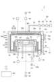
図1は、一つの例示的実施形態に係るプラズマ処理方法の流れ図である。図1に示すプラズマ処理方法(以下、「方法MT」という)は、容量結合型のプラズマ処理装置を用いて実行される。図2は、一つの例示的実施形態に係るプラズマ処理装置を概略的に示す図である。図2に示すプラズマ処理装置1は、容量結合型プラズマ処理装置である。プラズマ処理装置1は、方法MTの実行において用いられ得る。 FIG. 1 is a flow diagram of a plasma processing method according to one exemplary embodiment. The plasma processing method (hereinafter referred to as "method MT") shown in FIG. 1 is performed using a capacitively coupled plasma processing apparatus. FIG. 2 is a schematic diagram of a plasma processing apparatus according to one exemplary embodiment. The
プラズマ処理装置1は、チャンバ10を備えている。チャンバ10は、その中に内部空間10sを提供している。チャンバ10は、チャンバ本体12を含んでいる。チャンバ本体12は、略円筒形状を有している。内部空間10sは、チャンバ本体12の内側に提供されている。チャンバ本体12は、アルミニウムといった導体から形成されている。チャンバ本体12は、接地されている。チャンバ本体12の内壁面には、耐腐食性を有する膜が施されている。耐腐食性を有する膜は、酸化アルミニウム、酸化イットリウムといったセラミックから形成された膜であり得る。 The
チャンバ本体12の側壁には、通路12pが形成されている。基板Wは、内部空間10sとチャンバ10の外部との間で搬送されるときに、通路12pを通過する。通路12pは、ゲートバルブ12gにより開閉可能となっている。ゲートバルブ12gは、チャンバ本体12の側壁に沿って設けられている。 A
チャンバ本体12の底部上には、支持部13が設けられている。支持部13は、絶縁材料から形成されている。支持部13は、略円筒形状を有している。支持部13は、内部空間10sの中で、チャンバ本体12の底部から上方に延在している。支持部13は、基板支持器14を支持している。基板支持器14は、チャンバ10内、即ち内部空間10sの中で、基板Wを支持するように構成されている。 A
基板支持器14は、下部電極18及び静電チャック20を有している。下部電極18及び静電チャック20は、チャンバ10内に設けられている。基板支持器14は、電極プレート16を更に有し得る。電極プレート16は、例えばアルミニウムといった導体から形成されており、略円盤形状を有している。下部電極18は、電極プレート16上に設けられている。下部電極18は、例えばアルミニウムといった導体から形成されており、略円盤形状を有している。下部電極18は、電極プレート16に電気的に接続されている。 The
静電チャック20は、下部電極18上に設けられている。静電チャック20の上面の上には、基板Wが載置される。静電チャック20は、本体及び電極を有する。静電チャック20の本体は、誘電体から形成されている。静電チャック20の電極は、膜状の電極であり、静電チャック20の本体内に設けられている。静電チャック20の電極は、スイッチ20sを介して直流電源20pに接続されている。静電チャック20の電極に直流電源20pからの電圧が印加されると、静電チャック20と基板Wとの間で静電引力が発生する。発生した静電引力により、基板Wは、静電チャック20に引き付けられ、静電チャック20によって保持される。 An
基板支持器14上には、エッジリングERが配置される。エッジリングERは、限定されるものではないが、シリコン、炭化シリコン、又は石英から形成され得る。チャンバ10内において基板Wの処理が行われるときには、基板Wは、静電チャック20上、且つ、エッジリングERによって囲まれた領域内に、配置される。 An edge ring ER is arranged on the
下部電極18の内部には、流路18fが設けられている。流路18fには、チラーユニット22から配管22aを介して熱交換媒体(例えば冷媒)が供給される。チラーユニット22は、チャンバ10の外部に設けられている。流路18fに供給された熱交換媒体は、配管22bを介してチラーユニット22に戻される。プラズマ処理装置1では、静電チャック20上に載置された基板Wの温度が、熱交換媒体と下部電極18との熱交換により、調整される。 Inside the
プラズマ処理装置1は、ガス供給ライン24を更に備え得る。ガス供給ライン24は、伝熱ガス(例えばHeガス)を、静電チャック20の上面と基板Wの裏面との間に供給する。伝熱ガスは、伝熱ガス供給機構からガス供給ライン24に供給される。 The
プラズマ処理装置1は、上部電極30を更に備えている。上部電極30は、基板支持器14の上方に設けられている。上部電極30は、部材32を介して、チャンバ本体12の上部に支持されている。部材32は、絶縁性を有する材料から形成されている。上部電極30と部材32は、チャンバ本体12の上部開口を閉じている。 The
上部電極30は、天板34及び支持体36を含み得る。天板34の下面は、内部空間10sの側の下面であり、内部空間10sを画成している。天板34は、シリコン含有材料から形成されている。天板34は、例えばシリコン又は炭化シリコンから形成されている。天板34には、複数のガス吐出孔34aが形成されている。複数のガス吐出孔34aは、天板34をその板厚方向に貫通している。
支持体36は、天板34を着脱自在に支持する。支持体36は、アルミニウムといった導電性材料から形成される。支持体36の内部には、ガス拡散室36aが設けられている。支持体36には、複数のガス孔36bが形成されている。複数のガス孔36bは、ガス拡散室36aから下方に延びている。複数のガス孔36bは、複数のガス吐出孔34aにそれぞれ連通している。支持体36には、ガス導入口36cが形成されている。ガス導入口36cは、ガス拡散室36aに接続している。ガス導入口36cには、ガス供給管38が接続されている。 The
ガス供給管38には、バルブ群41、流量制御器群42、及びバルブ群43を介して、ガスソース群40が接続されている。ガスソース群40、バルブ群41、流量制御器群42、及びバルブ群43は、ガス供給部GSを構成している。ガスソース群40は、複数のガスソースを含んでいる。バルブ群41及びバルブ群43の各々は、複数の開閉バルブを含んでいる。流量制御器群42は、複数の流量制御器を含んでいる。流量制御器群42の複数の流量制御器の各々は、マスフローコントローラ又は圧力制御式の流量制御器である。ガスソース群40の複数のガスソースの各々は、バルブ群41の対応の開閉バルブ、流量制御器群42の対応の流量制御器、及びバルブ群43の対応の開閉バルブを介して、ガス供給管38に接続されている。 A
プラズマ処理装置1では、チャンバ本体12の内壁面に沿って、シールド46が着脱自在に設けられている。シールド46は、支持部13の外周にも設けられている。シールド46は、チャンバ本体12にプラズマ処理の副生物が付着することを防止する。シールド46は、接地されている。シールド46は、例えば、アルミニウムから形成された部材の表面に耐腐食性を有する膜を形成することにより構成される。耐腐食性を有する膜は、酸化イットリウムといったセラミックから形成された膜であり得る。なお、一実施形態において、シールド46は、チャンバ10の側壁が有する内壁面10wを提供している。内壁面10wは、第1の領域10a及び第2の領域10bを含んでいる。第1の領域10aは、内部空間10sの側方で延在している。第2の領域10bは、内部空間10sの上方且つ上部電極30の側方で延在している。第1の領域10a及び第2の領域10bは、シールド46ではなく、他の一つ以上の部材、例えば、チャンバ本体12によって提供されていてもよい。 A
支持部13とチャンバ本体12の側壁との間には、バッフルプレート48が設けられている。バッフルプレート48は、例えば、アルミニウムから形成された部材の表面に耐腐食性を有する膜を形成することにより構成される。耐腐食性を有する膜は、酸化イットリウムといったセラミックから形成された膜であり得る。バッフルプレート48には、複数の貫通孔が形成されている。バッフルプレート48の下方、且つ、チャンバ本体12の底部には、排気口12eが設けられている。排気口12eには、排気管52を介して排気装置50が接続されている。排気装置50は、圧力調整弁及びターボ分子ポンプといった真空ポンプを有している。 A
プラズマ処理装置1は、第1の高周波電源62及び第2の高周波電源64を更に備えている。第1の高周波電源62は、第1の高周波電力を発生する電源である。第1の高周波電力は、一例では、プラズマの生成に適した周波数を有する。第1の高周波電力の周波数は、例えば27MHz~100MHzの範囲内の周波数である。第1の高周波電源62は、整合器66を介して上部電極30に接続されている。整合器66は、第1の高周波電源62の出力インピーダンスと負荷側(上部電極30側)のインピーダンスを整合させるための回路を有している。なお、第1の高周波電源62は、整合器66及び電極プレート16を介して、下部電極18に接続されていてもよい。 The
第2の高周波電源64は、第2の高周波電力を発生する電源である。第2の高周波電力は、第1の高周波電力の周波数よりも低い周波数を有する。第2の高周波電力は、基板Wにイオンを引き込むためのバイアス用の高周波電力として用いられ得る。第2の高周波電力の周波数は、例えば400kHz~40MHzの範囲内の周波数である。第2の高周波電源64は、整合器68及び電極プレート16を介して下部電極18に接続されている。整合器68は、第2の高周波電源64の出力インピーダンスと負荷側(下部電極18側)のインピーダンスを整合させるための回路を有している。 The second high
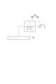
プラズマ処理装置1は、直流電源装置70を更に備えている。直流電源装置70は、上部電極30に電気的に接続されている。直流電源装置70は、パルス状の負極性の直流電圧を周期的に発生するように構成されている。図3は、図2に示すプラズマ処理装置の直流電源装置の構成の一例を示す図である。図4は、一つの例示的実施形態に係るプラズマ処理装置を用いて実行されるプラズマ処理方法のタイミングチャートである。図4において、横軸は時間を示している。図4において縦軸は、高周波電力(第1の高周波電力及び又は第2の高周波電力)の供給及び直流電源装置70の出力電圧を示している。図4において、高周波電力が高レベルであることは、高周波電力が供給されていることを表している。図4において、高周波電力が低レベルであることは、高周波電力が供給されていないことを表している。以下、図2と共に、図3及び図4を参照する。 The
一実施形態において、直流電源装置70は、可変直流電源70a及びスイッチングデバイス70bを有する。可変直流電源70aは、負極性の直流電圧を発生するように構成されている。可変直流電源70aが出力する負極性の直流電圧のレベルは、後述する制御部80によって制御され得る。スイッチングデバイス70bは、その導通状態の切り替えにより、可変直流電源70aと上部電極30との間の接続及び遮断を切り替える。スイッチングデバイス70bの導通状態の切り替えは、制御部80によって制御されてもよい。 In one embodiment, the
パルス状の負極性の直流電圧を周期的に出力するために、直流電源装置70の出力電圧は、周期PTにおける第1の期間P1では、負極性の直流電圧である。一実施形態においては、周期PT内の第1の期間P1では、可変直流電源70aと上部電極30を互いに接続するように、スイッチングデバイス70bの導通状態が切り替わる。直流電源装置70の出力電圧は、周期PTにおける残りの第2の期間P2では、ゼロボルトである。一実施形態においては、周期PT内の第2の期間P2では、可変直流電源70aと上部電極30との間の接続を遮断するよう、スイッチングデバイス70bの導通状態が切り替わる。 In order to periodically output a pulse-shaped negative DC voltage, the output voltage of the DC
一実施形態において、周期PTの逆数である周波数fは、400kHz以上であり得る。一実施形態において、周波数fは、1MHz以下であり得る。周波数fが1MHz以下である場合には、チャンバ10内でのラジカルの生成に対するイオンの挙動の独立性御性が高くなる。 In one embodiment, the frequency f, which is the reciprocal of the period PT, can be 400 kHz or greater. In one embodiment, frequency f may be 1 MHz or less. When the frequency f is 1 MHz or less, the independence of ion behavior with respect to radical generation in the
プラズマ処理装置1は、制御部80を更に備えている。制御部80は、プロセッサ、メモリといった記憶部、入力装置、表示装置、信号の入出力インターフェイス等を備えるコンピュータであり得る。制御部80は、プラズマ処理装置1の各部を制御する。制御部80では、オペレータが、プラズマ処理装置1を管理するためにコマンドの入力操作等を入力装置を用いて行うことができる。また、制御部80では、表示装置により、プラズマ処理装置1の可視化された稼働状況を表示することができる。さらに、制御部80の記憶部には、制御プログラム及びレシピデータが格納されている。制御プログラムは、プラズマ処理装置1で各種処理を実行するために、制御部80のプロセッサによって実行される。制御部80のプロセッサが、制御プログラムを実行し、レシピデータに従ってプラズマ処理装置1の各部を制御することにより、方法MTがプラズマ処理装置1で実行される。 The
以下、図1を再び参照して、それがプラズマ処理装置1を用いて実行される場合を例として、方法MTについて説明する。また、制御部80によるプラズマ処理装置1の各部の制御についても説明する。 Hereinafter, referring to FIG. 1 again, the method MT will be described using the
方法MTは、工程ST1及び工程ST2を含む。工程ST1及び工程ST2の実行中には、基板支持器14上に基板(例えば、ダミー基板)が載置されていてもよく、載置されていなくてもよい。 The method MT includes steps ST1 and ST2. A substrate (for example, a dummy substrate) may or may not be placed on the
工程ST1では、チャンバ10内で成膜ガスからプラズマが生成される。チャンバ10内で成膜ガスからプラズマを生成するために、工程ST1では、ガス供給部GSから成膜ガスがチャンバ10内に供給される。成膜ガスは、内壁面10wに形成される保護膜の原料を含むガスである。成膜ガスは、原料ガスとして、シリコン含有ガスを含み得る。この場合には、保護膜としてシリコン含有膜が形成される。シリコン含有ガスは、ハロゲン化ケイ素ガスであってもよい。ハロゲン化ケイ素ガスは、四塩化ケイ素ガスであってもよい。工程ST1では、原料ガスに加えて、一以上の別のガスがチャンバ10内に供給されてもよい。即ち、工程ST1では、原料ガスを含む混合ガスがチャンバ10内に供給されてもよい。一以上の別のガスは、酸素ガス及び希ガス(例えばアルゴンガス)であり得る。成膜ガスが酸素ガスを含む場合には、保護膜としてシリコン酸化膜が形成される。なお、成膜ガスは、シリコン含有ガスではなく、別の原料ガスを含んでいてもよい。例えば、成膜ガスは、原料ガスとして、炭素含有ガスを含んでいてもよい。この場合には、保護膜として炭素含有膜が形成される。炭素含有ガスは、CH4ガスといった炭化水素ガス又はC4F6ガスといったフルオロカーボンガスであり得る。また、工程ST1では、チャンバ10内で成膜ガスからプラズマを形成するために、第1の高周波電力及び/又は第2の高周波電力が供給される。その結果、チャンバ10内で成膜ガスからプラズマが生成される。なお、工程ST1では、第2の高周波電力は供給されなくてもよい。In step ST<b>1 , plasma is generated from the deposition gas within the
工程ST1の実行のために、制御部80は、成膜ガスをチャンバ10内に供給するようにガス供給部GSを制御する。工程ST1の実行のために、制御部80は、チャンバ10内の圧力を指定された圧力に設定するように排気装置50を制御する。工程ST1の実行のために、制御部80は、第1の高周波電力及び/又は第2の高周波電力を供給するように、第1の高周波電源62及び/又は第2の高周波電源64を制御する。 The
工程ST2は、工程ST1におけるプラズマの生成中に実行される。工程ST2では、工程ST1において成膜ガスから生成されたプラズマ中からの化学種を内壁面10w上に堆積させることにより、内壁面10w上に保護膜が形成される。工程ST2では、直流電源装置70からパルス状の負極性の直流電圧が上部電極30に周期的に印加される。上述したように、直流電源装置70の出力電圧は、周期PT内の第1の期間P1では、パルス状の負極性の直流電圧である。直流電源装置70の出力電圧は、周期PT内の残りの第2の期間P2では、ゼロボルトである。 Process ST2 is performed during plasma generation in process ST1. In step ST2, a protective film is formed on the
一実施形態では、工程ST2における直流電源装置70の出力電圧の実効値は、0Vよりも小さく-848V以上である。実効値は、パルス状の負極性の直流電圧のデューティー比(小数表現)の平方根と第1の期間P1におけるパルス状の負極性の直流電圧の値との間の積である。デューティー比は、周期PTの時間長に対する第1の期間P1の時間長の割合(小数表現)である。一実施形態において、パルス状の負極性の直流電圧のデューティー比は、0.2以上、0.5以下であり得る。一実施形態において、第1の期間P1におけるパルス状の負極性の直流電圧の値は、0Vよりも小さく、且つ、-1200V以上であり得る。 In one embodiment, the effective value of the output voltage of the
工程ST2の実行のために、制御部80は、パルス状の負極性の直流電圧を上部電極30に周期的に印加するように直流電源装置を制御する。一実施形態において、制御部80は、直流電源装置70の出力電圧の実効値を0Vよりも小さく-848V以上の値に設定するように直流電源装置70を制御する。 In order to perform step ST2, the
方法MTでは、成膜ガスから形成されたプラズマ中の原料は、上部電極30の表面及びチャンバ10の側壁の内壁面10w上に保護膜を形成する。保護膜の形成時にはパルス状の負極性の直流電圧が上部電極30に周期的に印加されるので、上部電極30の表面上に形成された保護膜に対するイオンのスパッタが生じる。その結果、上部電極30の表面上に形成された保護膜の厚みの増加が抑制される。一方、保護膜の形成時に直流電源装置70から上部電極30に印加される電圧の実効値に応じて、内壁面10w上に形成される保護膜の厚みが調整される。したがって、方法MTによれば、容量結合型のプラズマ処理装置1の上部電極30上に形成される保護膜の厚みの増加を抑制しつつ、内壁面10w上に形成される保護膜の厚みを制御することが可能となる。 In method MT, the material in the plasma formed from the deposition gas forms a protective film on the surface of the
一実施形態において、方法MTは、工程ST3を更に含んでいてもよい。工程ST3は、工程ST2の後に実行される。工程ST3では、チャンバ10内で基板のプラズマ処理が実行される。工程ST3の実行中には、基板が基板支持器14上に載置され、静電チャック20によって保持される。工程ST3において実行されるプラズマ処理は、プラズマエッチングであり得る。工程ST3において実行されるプラズマ処理は、他のプラズマ処理であってもよい。 In one embodiment, method MT may further include step ST3. Process ST3 is performed after process ST2. In step ST3, plasma processing of the substrate is performed within the
工程ST3では、ガス供給部GSからチャンバ10内に処理ガスが供給される。処理ガスは、基板に対して適用されるプラズマ処理に応じて適宜選択される。工程ST3では、チャンバ10内で処理ガスからプラズマを生成するために、第1の高周波電力及び/又は第2の高周波電力が供給される。その結果、チャンバ10内で処理ガスからプラズマが生成される。工程ST3では、処理ガスから生成されたプラズマからの化学種によって基板が処理される。工程ST3では、直流電源装置70の出力電圧の実効値は、工程ST2における実効値よりも小さい値に設定される。その結果、工程ST3の実行中の保護膜の減少が抑えられる。 In step ST3, the processing gas is supplied into the
工程ST3の実行のために、制御部80は、処理ガスをチャンバ10内に供給するようにガス供給部GSを制御する。工程ST3の実行のために、制御部80は、チャンバ10内の圧力を指定された圧力に設定するように排気装置50を制御する。工程ST3の実行のために、制御部80は、第1の高周波電力及び/又は第2の高周波電力を供給するように、第1の高周波電源62及び/又は第2の高周波電源64を制御する。また、工程ST3の実行のために、制御部80は、直流電源装置70の出力電圧の実効値を、工程ST2において設定された実効値よりも小さい値に設定するように直流電源装置70を制御する。 The
一実施形態において、方法MTは、工程ST4を更に含んでいてもよい。工程ST4では、工程ST2において形成された保護膜が除去される。工程ST4の実行中には、基板(例えば、ダミー基板)が基板支持器14上に載置されていてもよく、載置されていなくてもよい。 In one embodiment, method MT may further include step ST4. In step ST4, the protective film formed in step ST2 is removed. A substrate (for example, a dummy substrate) may or may not be placed on the
工程ST4においては、ガス供給部GSからチャンバ10内にクリーニングガスが供給される。クリーニングガスは、保護膜がシリコン酸化膜である場合には、フルオロカーボンガス(例えばCF4ガス)を含み得る。クリーニングガスは、保護膜が炭素含有膜である場合には、酸素含有ガス(例えばO2ガス)を含み得る。工程ST4では、チャンバ10内でクリーニングガスからプラズマを生成するために、第1の高周波電力及び/又は第2の高周波電力が供給される。その結果、チャンバ10内でクリーニングガスからプラズマが生成される。工程ST4では、クリーニングガスから生成されたプラズマからの化学種によって保護膜が除去される。この工程ST4では、直流電源装置70の出力電圧の実効値は、工程ST2における実効値よりも大きい値に設定される。その結果、工程ST4における保護膜の除去の効率が高められる。In step ST4, a cleaning gas is supplied into the
工程ST4の実行のために、制御部80は、クリーニングガスをチャンバ10内に供給するようにガス供給部GSを制御する。工程ST4の実行のために、制御部80は、チャンバ10内の圧力を指定された圧力に設定するように排気装置50を制御する。工程ST4の実行のために、制御部80は、第1の高周波電力及び/又は第2の高周波電力を供給するように、第1の高周波電源62及び/又は第2の高周波電源64を制御する。また、工程ST4の実行のために、制御部80は、直流電源装置70の出力電圧の実効値を、工程ST2において設定された実効値よりも大きい値に設定するように直流電源装置70を制御する。 In order to perform step ST4, the
一実施形態において、方法MTは、工程ST5を更に含み得る。工程ST5では停止条件が満たされるか否かが判定される。停止条件は、例えば、工程ST1~工程ST4を含むシーケンスの実行回数が所定回数に達している場合には、満たされているものと判定される。工程ST5において停止条件が満たされていないと判定された場合には、工程ST1~工程ST4を含むシーケンスが更に実行される。更に実行されるシーケンス中の工程ST3では、先のシーケンス中の工程ST3において処理された基板に対するプラズマ処理が更に実行されるか、別の基板に対するプラズマ処理が実行される。工程ST5において停止条件が満たされていると判定された場合には、方法MTは終了する。 In one embodiment, method MT may further include step ST5. In step ST5, it is determined whether or not a stop condition is satisfied. The stop condition is determined to be satisfied, for example, when the number of executions of the sequence including steps ST1 to ST4 has reached a predetermined number. When it is determined in step ST5 that the stop condition is not satisfied, a sequence including steps ST1 to ST4 is further executed. In step ST3 in the sequence that is further performed, the substrate processed in step ST3 in the previous sequence is further subjected to plasma processing, or another substrate is subjected to plasma processing. If it is determined in step ST5 that the stopping condition is satisfied, the method MT ends.
以上、種々の例示的実施形態について説明してきたが、上述した例示的実施形態に限定されることなく、様々な省略、置換、及び変更がなされてもよい。また、異なる実施形態における要素を組み合わせて他の実施形態を形成することが可能である。 While various exemplary embodiments have been described above, various omissions, substitutions, and modifications may be made without being limited to the exemplary embodiments described above. Also, elements from different embodiments can be combined to form other embodiments.
以下、方法MT及びプラズマ処理装置1の評価のために行った実験について説明する。なお、本開示は以下に説明する実験により限定されるものではない。 Experiments conducted to evaluate the method MT and the
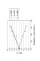
実験では、上部電極30の内部空間10s側の表面に第1のチップを、第1の領域10aに第2のチップを、第2の領域10bに第3のチップを貼り付けた状態で、工程ST1及び工程ST2を実行した。実験では、工程ST2における直流電源装置70の出力電圧の実効値を種々の値に設定した。実験における工程ST1の条件を以下に示す。
<工程ST1の条件>
・チャンバ10内の圧力:20mTorr(2.666Pa)
・四塩化ケイ素ガスの流量:5sccm
・酸素ガスの流量:50sccm
・アルゴンガスの流量:250sccm
・第1の高周波電力:60MHz、1000W
・第2の高周波電力:0W
・周波数f(周期PTの逆数):400kHz
・パルス状の負極性の直流電圧のデューティー比:0.3又は0.5
・パルス状の負極性の直流電圧の値:0V、-500V、又は-900VIn the experiment, the first chip was attached to the
<Conditions of step ST1>
・Pressure in chamber 10: 20 mTorr (2.666 Pa)
・Flow rate of silicon tetrachloride gas: 5 sccm
・Flow rate of oxygen gas: 50 sccm
・Flow rate of argon gas: 250 sccm
・First high-frequency power: 60 MHz, 1000 W
・Second high frequency power: 0 W
・Frequency f (reciprocal of period PT): 400 kHz
・Duty ratio of pulsed negative DC voltage: 0.3 or 0.5
・Pulse-shaped negative DC voltage value: 0 V, -500 V, or -900 V
実験では、直流電源装置70の出力電圧の実効値の各設定の下で各チップ上に形成された保護膜の膜厚を測定した。そして、各チップ状に形成された保護膜の膜厚の基準膜厚に対する比、即ち膜厚比(百分率)を求めた。ここで、基準膜厚は、工程ST2における直流電源装置70の出力電圧の実効値が0Vであるときに同じ箇所に貼り付けられたチップ上に形成された保護膜の膜厚である。 In the experiment, the film thickness of the protective film formed on each chip was measured under each setting of the effective value of the output voltage of the
図5に実験の結果を表すグラフを示す。図5のグラフにおいて、横軸は、工程ST2における直流電源装置70の出力電圧の実効値を示している。図5のグラフにおいて縦軸は、求めた膜厚比を示している。図5において、第1~第3の膜厚比は第1~第3のチップ上にそれぞれ形成された保護膜の膜厚比を示している。図5に示すように、直流電源装置70の出力電圧の実効値の絶対値の増加につれて、第1の膜厚比が減少していた。このことから、成膜ガスのプラズマの生成中に直流電源装置70からパルス状の負極性の直流電圧を上部電極30に周期的に印加することにより、上部電極30の表面上に形成される保護膜の膜厚の増加を抑制可能であることが確認された。また、直流電源装置70の出力電圧の実効値の絶対値の増加につれて、上部電極30の表面上に形成される保護膜の膜厚が減少することが確認された。 FIG. 5 shows a graph representing the results of the experiment. In the graph of FIG. 5, the horizontal axis indicates the effective value of the output voltage of
一方、図5に示すように、直流電源装置70の出力電圧の実効値の絶対値の増加につれて、第2の膜厚比及び第3の膜厚比が増加していた。このことから、保護膜の形成時に直流電源装置70から上部電極に印加される電圧の実効値に応じて、チャンバ10の側壁の内壁面10w上に形成される保護膜の厚みを調整可能であることが確認された。 On the other hand, as shown in FIG. 5, the second film thickness ratio and the third film thickness ratio increased as the absolute value of the effective value of the output voltage of the DC
以上の説明から、本開示の種々の実施形態は、説明の目的で本明細書で説明されており、本開示の範囲及び主旨から逸脱することなく種々の変更をなし得ることが、理解されるであろう。したがって、本明細書に開示した種々の実施形態は限定することを意図しておらず、真の範囲と主旨は、添付の特許請求の範囲によって示される。 From the foregoing description, it will be appreciated that various embodiments of the present disclosure have been set forth herein for purposes of illustration, and that various changes may be made without departing from the scope and spirit of the present disclosure. Will. Therefore, the various embodiments disclosed herein are not intended to be limiting, with a true scope and spirit being indicated by the following claims.
1…プラズマ処理装置、10…チャンバ、14…基板支持器、18…下部電極、30…上部電極、62…第1の高周波電源、64…第2の高周波電源、70…直流電源装置。 DESCRIPTION OF
Claims (11)
Translated fromJapanese前記プラズマ処理装置は、
内壁面を有する側壁を含むチャンバと、
前記チャンバ内に設けられた下部電極を含む基板支持器と、
前記基板支持器の上方に設けられた上部電極と、
前記チャンバ内でプラズマを生成するための高周波電源と、
前記上部電極に電気的に接続された直流電源装置と、
を備え、
前記直流電源装置は、パルス状の負極性の直流電圧を周期的に発生するように構成されており、
該プラズマ処理方法は、
前記高周波電源から高周波電力を供給することにより、前記チャンバ内で成膜ガスからプラズマを生成する工程と、
前記プラズマからの化学種を前記内壁面上に堆積させることにより、前記内壁面上に保護膜を形成する工程と、
を含み、
保護膜を形成する前記工程において、前記直流電源装置から前記パルス状の負極性の直流電圧が前記上部電極に周期的に印加される、
プラズマ処理方法。A plasma processing method performed using a plasma processing apparatus,
The plasma processing apparatus is
a chamber including a sidewall having an inner wall surface;
a substrate support including a lower electrode disposed within the chamber;
an upper electrode provided above the substrate support;
a radio frequency power source for generating a plasma within the chamber;
a DC power supply electrically connected to the upper electrode;
with
The DC power supply is configured to periodically generate a pulsed negative DC voltage,
The plasma treatment method comprises
generating plasma from the deposition gas in the chamber by supplying high-frequency power from the high-frequency power supply;
forming a protective film on the inner wall surface by depositing species from the plasma on the inner wall surface;
including
In the step of forming the protective film, the pulsed negative DC voltage is periodically applied to the upper electrode from the DC power supply.
Plasma treatment method.
前記実効値は、前記周期の時間長に対する前記第1の期間の時間長の割合であるデューティー比の平方根と前記第1の期間における前記パルス状の負極性の直流電圧の値との間の積である、
請求項7に記載のプラズマ処理方法。The effective value of the output voltage of the DC power supply in the step of forming the protective film is less than 0 V and -848 V or more,
The effective value is the product of the square root of the duty ratio, which is the ratio of the time length of the first period to the time length of the cycle, and the value of the pulse-shaped negative polarity DC voltage in the first period. is
The plasma processing method according to claim 7.
プラズマ処理を実行する前記工程において、
前記高周波電源から高周波電力を供給することにより前記チャンバ内で処理ガスからプラズマが生成され、
前記直流電源装置の前記出力電圧の前記実効値が、保護膜を形成する前記工程における前記実効値よりも小さい値に設定され、
前記処理ガスから生成された前記プラズマからの化学種によって前記基板が処理される、
請求項8に記載のプラズマ処理方法。further comprising performing a plasma treatment of the substrate in the chamber after the step of forming a protective film;
In the step of performing plasma treatment,
Plasma is generated from the processing gas in the chamber by supplying high-frequency power from the high-frequency power supply,
wherein the effective value of the output voltage of the DC power supply is set to a value smaller than the effective value in the step of forming a protective film;
the substrate is processed with species from the plasma generated from the process gas;
The plasma processing method according to claim 8.
前記保護膜を除去する前記工程において、
前記高周波電源から高周波電力を供給することにより前記チャンバ内でクリーニングガスからプラズマが生成され、
前記直流電源装置の前記出力電圧の前記実効値が、保護膜を形成する前記工程における前記実効値よりも大きい値に設定され、
前記クリーニングガスから生成された前記プラズマからの化学種によって前記保護膜が処理される、
請求項8又は9に記載のプラズマ処理方法。further comprising removing the protective film;
In the step of removing the protective film,
Plasma is generated from the cleaning gas in the chamber by supplying high-frequency power from the high-frequency power supply,
wherein the effective value of the output voltage of the DC power supply is set to a value larger than the effective value in the step of forming a protective film;
the protective film is treated with species from the plasma generated from the cleaning gas;
The plasma processing method according to claim 8 or 9.
前記チャンバ内に設けられた下部電極を含む基板支持器と、
前記基板支持器の上方に設けられた上部電極と、
前記チャンバ内でプラズマを生成するための高周波電源と、
前記上部電極に電気的に接続された直流電源装置と、
前記高周波電源及び前記直流電源装置を制御するように構成された制御部と、
を備え、
前記直流電源装置は、パルス状の負極性の直流電圧を周期的に発生するように構成されており、
前記制御部は、
前記チャンバ内で成膜ガスからプラズマを生成するために高周波電力を供給するように前記高周波電源を制御し、
前記プラズマからの化学種を前記内壁面上に堆積させることにより前記内壁面上に保護膜を形成するために前記パルス状の負極性の直流電圧を前記上部電極に周期的に印加するように前記直流電源装置を制御する、
プラズマ処理装置。a chamber including a sidewall having an inner wall surface;
a substrate support including a lower electrode disposed within the chamber;
an upper electrode provided above the substrate support;
a radio frequency power source for generating a plasma within the chamber;
a DC power supply electrically connected to the upper electrode;
a control unit configured to control the high-frequency power supply and the DC power supply;
with
The DC power supply is configured to periodically generate a pulsed negative DC voltage,
The control unit
controlling the high-frequency power supply to supply high-frequency power to generate plasma from the deposition gas in the chamber;
said step of periodically applying said pulsed negative DC voltage to said upper electrode to deposit chemical species from said plasma on said inner wall surface to form a protective film on said inner wall surface; to control a DC power supply,
Plasma processing equipment.
Priority Applications (8)
| Application Number | Priority Date | Filing Date | Title |
|---|---|---|---|
| JP2019112618AJP7220626B2 (en) | 2019-06-18 | 2019-06-18 | Plasma processing method and plasma processing apparatus |
| KR1020200068436AKR20200144479A (en) | 2019-06-18 | 2020-06-05 | Plasma processing method and plasma processing apparatus |
| CN202010511382.XACN112103165B (en) | 2019-06-18 | 2020-06-08 | Plasma processing method and plasma processing device |
| SG10202005364XASG10202005364XA (en) | 2019-06-18 | 2020-06-08 | Plasma processing method and plasma processing apparatus |
| CN202411207915.XACN119092390A (en) | 2019-06-18 | 2020-06-08 | Plasma processing method and plasma processing device |
| TW113142336ATW202523902A (en) | 2019-06-18 | 2020-06-09 | Plasma processing method and plasma processing apparatus |
| US16/896,304US11251048B2 (en) | 2019-06-18 | 2020-06-09 | Plasma processing method and plasma processing apparatus |
| TW109119299ATWI865541B (en) | 2019-06-18 | 2020-06-09 | Plasma processing method and plasma processing apparatus |
Applications Claiming Priority (1)
| Application Number | Priority Date | Filing Date | Title |
|---|---|---|---|
| JP2019112618AJP7220626B2 (en) | 2019-06-18 | 2019-06-18 | Plasma processing method and plasma processing apparatus |
Publications (2)
| Publication Number | Publication Date |
|---|---|
| JP2020205361A JP2020205361A (en) | 2020-12-24 |
| JP7220626B2true JP7220626B2 (en) | 2023-02-10 |
Family
ID=73749669
Family Applications (1)
| Application Number | Title | Priority Date | Filing Date |
|---|---|---|---|
| JP2019112618AActiveJP7220626B2 (en) | 2019-06-18 | 2019-06-18 | Plasma processing method and plasma processing apparatus |
Country Status (6)
| Country | Link |
|---|---|
| US (1) | US11251048B2 (en) |
| JP (1) | JP7220626B2 (en) |
| KR (1) | KR20200144479A (en) |
| CN (2) | CN112103165B (en) |
| SG (1) | SG10202005364XA (en) |
| TW (2) | TW202523902A (en) |
Families Citing this family (5)
| Publication number | Priority date | Publication date | Assignee | Title |
|---|---|---|---|---|
| JP7158308B2 (en)* | 2019-02-14 | 2022-10-21 | 東京エレクトロン株式会社 | Plasma processing apparatus and plasma processing method |
| CN115692190A (en) | 2021-07-28 | 2023-02-03 | 东京毅力科创株式会社 | Plasma processing method, plasma processing device and system |
| JP7679337B2 (en)* | 2021-07-28 | 2025-05-19 | 東京エレクトロン株式会社 | Plasma processing method and plasma processing apparatus |
| JP7671684B2 (en)* | 2021-11-30 | 2025-05-02 | 東京エレクトロン株式会社 | Etching method and plasma processing apparatus |
| JP2023130163A (en)* | 2022-03-07 | 2023-09-20 | キオクシア株式会社 | Cleaning method, method of manufacturing semiconductor device, plasma treatment device, and outer circumferential ring set |
Citations (5)
| Publication number | Priority date | Publication date | Assignee | Title |
|---|---|---|---|---|
| US20060037701A1 (en) | 2004-06-21 | 2006-02-23 | Tokyo Electron Limited | Plasma processing apparatus and method |
| JP2006270018A (en) | 2004-06-21 | 2006-10-05 | Tokyo Electron Ltd | Plasma processing apparatus, plasma processing method, and computer-readable storage medium |
| JP2013033856A (en) | 2011-08-02 | 2013-02-14 | Tokyo Electron Ltd | Plasma etching method |
| JP2014082228A (en) | 2012-10-12 | 2014-05-08 | Tokyo Electron Ltd | Plasma etching method |
| JP2016012712A (en) | 2014-06-02 | 2016-01-21 | 東京エレクトロン株式会社 | Plasma processing method and plasma processing device |
Family Cites Families (11)
| Publication number | Priority date | Publication date | Assignee | Title |
|---|---|---|---|---|
| JP4628696B2 (en)* | 2004-06-03 | 2011-02-09 | 東京エレクトロン株式会社 | Plasma CVD equipment |
| TWI574318B (en)* | 2004-06-21 | 2017-03-11 | Tokyo Electron Ltd | A plasma processing apparatus, a plasma processing method, and a computer-readable recording medium |
| US8753724B2 (en)* | 2012-09-26 | 2014-06-17 | Front Edge Technology Inc. | Plasma deposition on a partially formed battery through a mesh screen |
| JP5956933B2 (en) | 2013-01-15 | 2016-07-27 | 東京エレクトロン株式会社 | Plasma processing method and plasma processing apparatus |
| JP6320248B2 (en)* | 2014-03-04 | 2018-05-09 | 東京エレクトロン株式会社 | Plasma etching method |
| JP6632426B2 (en)* | 2016-02-29 | 2020-01-22 | 東京エレクトロン株式会社 | Plasma processing apparatus and precoat processing method |
| KR102139245B1 (en)* | 2016-06-20 | 2020-07-29 | 어플라이드 머티어리얼스, 인코포레이티드 | Cleaning process to remove boron-carbon residues in the processing chamber at high temperatures |
| JP6826955B2 (en)* | 2017-06-14 | 2021-02-10 | 東京エレクトロン株式会社 | Plasma processing equipment and plasma processing method |
| JP2019008945A (en)* | 2017-06-22 | 2019-01-17 | 東京エレクトロン株式会社 | Antenna and plasma processing apparatus |
| JP7045152B2 (en)* | 2017-08-18 | 2022-03-31 | 東京エレクトロン株式会社 | Plasma processing method and plasma processing equipment |
| US10727075B2 (en)* | 2017-12-22 | 2020-07-28 | Applied Materials, Inc. | Uniform EUV photoresist patterning utilizing pulsed plasma process |
- 2019
- 2019-06-18JPJP2019112618Apatent/JP7220626B2/enactiveActive
- 2020
- 2020-06-05KRKR1020200068436Apatent/KR20200144479A/enactivePending
- 2020-06-08CNCN202010511382.XApatent/CN112103165B/enactiveActive
- 2020-06-08CNCN202411207915.XApatent/CN119092390A/enactivePending
- 2020-06-08SGSG10202005364XApatent/SG10202005364XA/enunknown
- 2020-06-09USUS16/896,304patent/US11251048B2/enactiveActive
- 2020-06-09TWTW113142336Apatent/TW202523902A/enunknown
- 2020-06-09TWTW109119299Apatent/TWI865541B/enactive
Patent Citations (6)
| Publication number | Priority date | Publication date | Assignee | Title |
|---|---|---|---|---|
| US20060037701A1 (en) | 2004-06-21 | 2006-02-23 | Tokyo Electron Limited | Plasma processing apparatus and method |
| JP2006270018A (en) | 2004-06-21 | 2006-10-05 | Tokyo Electron Ltd | Plasma processing apparatus, plasma processing method, and computer-readable storage medium |
| JP2013033856A (en) | 2011-08-02 | 2013-02-14 | Tokyo Electron Ltd | Plasma etching method |
| JP2014082228A (en) | 2012-10-12 | 2014-05-08 | Tokyo Electron Ltd | Plasma etching method |
| US20150340243A1 (en) | 2012-10-12 | 2015-11-26 | Tokyo Electron Limited | Plasma etching method |
| JP2016012712A (en) | 2014-06-02 | 2016-01-21 | 東京エレクトロン株式会社 | Plasma processing method and plasma processing device |
Also Published As
| Publication number | Publication date |
|---|---|
| US11251048B2 (en) | 2022-02-15 |
| TW202102717A (en) | 2021-01-16 |
| KR20200144479A (en) | 2020-12-29 |
| CN119092390A (en) | 2024-12-06 |
| JP2020205361A (en) | 2020-12-24 |
| US20200402805A1 (en) | 2020-12-24 |
| TW202523902A (en) | 2025-06-16 |
| CN112103165B (en) | 2024-09-20 |
| CN112103165A (en) | 2020-12-18 |
| SG10202005364XA (en) | 2021-01-28 |
| TWI865541B (en) | 2024-12-11 |
Similar Documents
| Publication | Publication Date | Title |
|---|---|---|
| JP7220626B2 (en) | Plasma processing method and plasma processing apparatus | |
| TWI664676B (en) | Etching method | |
| KR102538188B1 (en) | Plasma processing apparatus cleaning method | |
| CN112530799B (en) | Method for etching silicon oxide film and plasma processing apparatus | |
| CN110021524B (en) | Etching method | |
| TW202044405A (en) | Cleaning method and plasma processing apparatus | |
| JP7158308B2 (en) | Plasma processing apparatus and plasma processing method | |
| CN111048389A (en) | Plasma processing method and plasma processing apparatus | |
| JP7203531B2 (en) | Plasma processing method and plasma processing apparatus | |
| CN112420507B (en) | Method for processing substrate, device manufacturing method and plasma processing apparatus | |
| JP6960421B2 (en) | Plasma processing equipment and plasma processing method | |
| CN112951698B (en) | Plasma processing method and plasma processing apparatus | |
| JP2021114551A (en) | Etching method and plasma processing device | |
| TW202205348A (en) | Edge ring and plasma processing apparatus |
Legal Events
| Date | Code | Title | Description |
|---|---|---|---|
| A621 | Written request for application examination | Free format text:JAPANESE INTERMEDIATE CODE: A621 Effective date:20220324 | |
| A977 | Report on retrieval | Free format text:JAPANESE INTERMEDIATE CODE: A971007 Effective date:20221215 | |
| TRDD | Decision of grant or rejection written | ||
| A01 | Written decision to grant a patent or to grant a registration (utility model) | Free format text:JAPANESE INTERMEDIATE CODE: A01 Effective date:20230104 | |
| A61 | First payment of annual fees (during grant procedure) | Free format text:JAPANESE INTERMEDIATE CODE: A61 Effective date:20230131 | |
| R150 | Certificate of patent or registration of utility model | Ref document number:7220626 Country of ref document:JP Free format text:JAPANESE INTERMEDIATE CODE: R150 |