JP7220251B2 - middle ring - Google Patents
middle ringDownload PDFInfo
- Publication number
- JP7220251B2 JP7220251B2JP2021075777AJP2021075777AJP7220251B2JP 7220251 B2JP7220251 B2JP 7220251B2JP 2021075777 AJP2021075777 AJP 2021075777AJP 2021075777 AJP2021075777 AJP 2021075777AJP 7220251 B2JP7220251 B2JP 7220251B2
- Authority
- JP
- Japan
- Prior art keywords
- ring
- edge ring
- edge
- middle ring
- guide structure
- Prior art date
- Legal status (The legal status is an assumption and is not a legal conclusion. Google has not performed a legal analysis and makes no representation as to the accuracy of the status listed.)
- Active
Links
- 239000000758substrateSubstances0.000claimsdescription129
- 238000012545processingMethods0.000description74
- 239000000919ceramicSubstances0.000description46
- 239000010410layerSubstances0.000description45
- 238000000034methodMethods0.000description34
- 230000008569processEffects0.000description27
- 239000007789gasSubstances0.000description25
- 239000012212insulatorSubstances0.000description24
- 235000012431wafersNutrition0.000description19
- 238000004519manufacturing processMethods0.000description15
- 239000004065semiconductorSubstances0.000description15
- 230000000295complement effectEffects0.000description13
- 239000000463materialSubstances0.000description12
- 238000010586diagramMethods0.000description11
- 238000010438heat treatmentMethods0.000description11
- 239000002826coolantSubstances0.000description8
- 230000003628erosive effectEffects0.000description8
- 238000012546transferMethods0.000description7
- 238000000231atomic layer depositionMethods0.000description6
- 238000005229chemical vapour depositionMethods0.000description6
- 238000005530etchingMethods0.000description6
- 239000012790adhesive layerSubstances0.000description5
- 230000008859changeEffects0.000description5
- VYPSYNLAJGMNEJ-UHFFFAOYSA-Nsilicon dioxideInorganic materialsO=[Si]=OVYPSYNLAJGMNEJ-UHFFFAOYSA-N0.000description5
- 238000009826distributionMethods0.000description4
- 239000002184metalSubstances0.000description4
- 229910052751metalInorganic materials0.000description4
- 238000005240physical vapour depositionMethods0.000description4
- 230000007704transitionEffects0.000description4
- 238000004140cleaningMethods0.000description3
- 238000000151depositionMethods0.000description3
- 230000008021depositionEffects0.000description3
- 238000011065in-situ storageMethods0.000description3
- 239000000203mixtureSubstances0.000description3
- 238000010926purgeMethods0.000description3
- 235000012239silicon dioxideNutrition0.000description3
- 238000001816coolingMethods0.000description2
- 239000012530fluidSubstances0.000description2
- 230000006870functionEffects0.000description2
- 239000007943implantSubstances0.000description2
- 238000007689inspectionMethods0.000description2
- 238000009434installationMethods0.000description2
- 230000010354integrationEffects0.000description2
- 238000005468ion implantationMethods0.000description2
- 238000005259measurementMethods0.000description2
- 150000002739metalsChemical class0.000description2
- 238000012986modificationMethods0.000description2
- 230000004048modificationEffects0.000description2
- NJPPVKZQTLUDBO-UHFFFAOYSA-NnovaluronChemical compoundC1=C(Cl)C(OC(F)(F)C(OC(F)(F)F)F)=CC=C1NC(=O)NC(=O)C1=C(F)C=CC=C1FNJPPVKZQTLUDBO-UHFFFAOYSA-N0.000description2
- -1oxidesSubstances0.000description2
- 238000007747platingMethods0.000description2
- 238000012805post-processingMethods0.000description2
- 229910052710siliconInorganic materials0.000description2
- 239000010703siliconSubstances0.000description2
- 239000000377silicon dioxideSubstances0.000description2
- 239000012159carrier gasSubstances0.000description1
- 230000005465channelingEffects0.000description1
- 238000006243chemical reactionMethods0.000description1
- 239000004020conductorSubstances0.000description1
- 238000006073displacement reactionMethods0.000description1
- 238000009616inductively coupled plasmaMethods0.000description1
- 238000002347injectionMethods0.000description1
- 239000007924injectionSubstances0.000description1
- 239000002245particleSubstances0.000description1
- 239000002243precursorSubstances0.000description1
- 230000001681protective effectEffects0.000description1
- 239000010453quartzSubstances0.000description1
- 239000000376reactantSubstances0.000description1
- 230000004044responseEffects0.000description1
- 229910052594sapphireInorganic materials0.000description1
- 239000010980sapphireSubstances0.000description1
- 238000000926separation methodMethods0.000description1
- HBMJWWWQQXIZIP-UHFFFAOYSA-Nsilicon carbideChemical compound[Si+]#[C-]HBMJWWWQQXIZIP-UHFFFAOYSA-N0.000description1
- 229910010271silicon carbideInorganic materials0.000description1
- 238000013022ventingMethods0.000description1
- RUDFQVOCFDJEEF-UHFFFAOYSA-Nyttrium(III) oxideInorganic materials[O-2].[O-2].[O-2].[Y+3].[Y+3]RUDFQVOCFDJEEF-UHFFFAOYSA-N0.000description1
Images


Classifications
- H—ELECTRICITY
- H01—ELECTRIC ELEMENTS
- H01J—ELECTRIC DISCHARGE TUBES OR DISCHARGE LAMPS
- H01J37/00—Discharge tubes with provision for introducing objects or material to be exposed to the discharge, e.g. for the purpose of examination or processing thereof
- H01J37/32—Gas-filled discharge tubes
- H01J37/32431—Constructional details of the reactor
- H01J37/32623—Mechanical discharge control means
- H01J37/32642—Focus rings
- H—ELECTRICITY
- H01—ELECTRIC ELEMENTS
- H01L—SEMICONDUCTOR DEVICES NOT COVERED BY CLASS H10
- H01L21/00—Processes or apparatus adapted for the manufacture or treatment of semiconductor or solid state devices or of parts thereof
- H01L21/67—Apparatus specially adapted for handling semiconductor or electric solid state devices during manufacture or treatment thereof; Apparatus specially adapted for handling wafers during manufacture or treatment of semiconductor or electric solid state devices or components ; Apparatus not specifically provided for elsewhere
- H01L21/683—Apparatus specially adapted for handling semiconductor or electric solid state devices during manufacture or treatment thereof; Apparatus specially adapted for handling wafers during manufacture or treatment of semiconductor or electric solid state devices or components ; Apparatus not specifically provided for elsewhere for supporting or gripping
- H01L21/687—Apparatus specially adapted for handling semiconductor or electric solid state devices during manufacture or treatment thereof; Apparatus specially adapted for handling wafers during manufacture or treatment of semiconductor or electric solid state devices or components ; Apparatus not specifically provided for elsewhere for supporting or gripping using mechanical means, e.g. chucks, clamps or pinches
- H01L21/68714—Apparatus specially adapted for handling semiconductor or electric solid state devices during manufacture or treatment thereof; Apparatus specially adapted for handling wafers during manufacture or treatment of semiconductor or electric solid state devices or components ; Apparatus not specifically provided for elsewhere for supporting or gripping using mechanical means, e.g. chucks, clamps or pinches the wafers being placed on a susceptor, stage or support
- H01L21/68735—Apparatus specially adapted for handling semiconductor or electric solid state devices during manufacture or treatment thereof; Apparatus specially adapted for handling wafers during manufacture or treatment of semiconductor or electric solid state devices or components ; Apparatus not specifically provided for elsewhere for supporting or gripping using mechanical means, e.g. chucks, clamps or pinches the wafers being placed on a susceptor, stage or support characterised by edge profile or support profile
- H—ELECTRICITY
- H01—ELECTRIC ELEMENTS
- H01J—ELECTRIC DISCHARGE TUBES OR DISCHARGE LAMPS
- H01J37/00—Discharge tubes with provision for introducing objects or material to be exposed to the discharge, e.g. for the purpose of examination or processing thereof
- H01J37/32—Gas-filled discharge tubes
- H01J37/32431—Constructional details of the reactor
- H01J37/32715—Workpiece holder
- H—ELECTRICITY
- H01—ELECTRIC ELEMENTS
- H01L—SEMICONDUCTOR DEVICES NOT COVERED BY CLASS H10
- H01L21/00—Processes or apparatus adapted for the manufacture or treatment of semiconductor or solid state devices or of parts thereof
- H01L21/67—Apparatus specially adapted for handling semiconductor or electric solid state devices during manufacture or treatment thereof; Apparatus specially adapted for handling wafers during manufacture or treatment of semiconductor or electric solid state devices or components ; Apparatus not specifically provided for elsewhere
- H01L21/67005—Apparatus not specifically provided for elsewhere
- H01L21/67011—Apparatus for manufacture or treatment
- H01L21/67017—Apparatus for fluid treatment
- H01L21/67063—Apparatus for fluid treatment for etching
- H01L21/67069—Apparatus for fluid treatment for etching for drying etching
- H—ELECTRICITY
- H01—ELECTRIC ELEMENTS
- H01L—SEMICONDUCTOR DEVICES NOT COVERED BY CLASS H10
- H01L21/00—Processes or apparatus adapted for the manufacture or treatment of semiconductor or solid state devices or of parts thereof
- H01L21/67—Apparatus specially adapted for handling semiconductor or electric solid state devices during manufacture or treatment thereof; Apparatus specially adapted for handling wafers during manufacture or treatment of semiconductor or electric solid state devices or components ; Apparatus not specifically provided for elsewhere
- H01L21/67005—Apparatus not specifically provided for elsewhere
- H01L21/67011—Apparatus for manufacture or treatment
- H01L21/67098—Apparatus for thermal treatment
- H01L21/67115—Apparatus for thermal treatment mainly by radiation
- H—ELECTRICITY
- H01—ELECTRIC ELEMENTS
- H01L—SEMICONDUCTOR DEVICES NOT COVERED BY CLASS H10
- H01L21/00—Processes or apparatus adapted for the manufacture or treatment of semiconductor or solid state devices or of parts thereof
- H01L21/67—Apparatus specially adapted for handling semiconductor or electric solid state devices during manufacture or treatment thereof; Apparatus specially adapted for handling wafers during manufacture or treatment of semiconductor or electric solid state devices or components ; Apparatus not specifically provided for elsewhere
- H01L21/683—Apparatus specially adapted for handling semiconductor or electric solid state devices during manufacture or treatment thereof; Apparatus specially adapted for handling wafers during manufacture or treatment of semiconductor or electric solid state devices or components ; Apparatus not specifically provided for elsewhere for supporting or gripping
- H01L21/6835—Apparatus specially adapted for handling semiconductor or electric solid state devices during manufacture or treatment thereof; Apparatus specially adapted for handling wafers during manufacture or treatment of semiconductor or electric solid state devices or components ; Apparatus not specifically provided for elsewhere for supporting or gripping using temporarily an auxiliary support
- H—ELECTRICITY
- H01—ELECTRIC ELEMENTS
- H01L—SEMICONDUCTOR DEVICES NOT COVERED BY CLASS H10
- H01L21/00—Processes or apparatus adapted for the manufacture or treatment of semiconductor or solid state devices or of parts thereof
- H01L21/67—Apparatus specially adapted for handling semiconductor or electric solid state devices during manufacture or treatment thereof; Apparatus specially adapted for handling wafers during manufacture or treatment of semiconductor or electric solid state devices or components ; Apparatus not specifically provided for elsewhere
- H01L21/683—Apparatus specially adapted for handling semiconductor or electric solid state devices during manufacture or treatment thereof; Apparatus specially adapted for handling wafers during manufacture or treatment of semiconductor or electric solid state devices or components ; Apparatus not specifically provided for elsewhere for supporting or gripping
- H01L21/687—Apparatus specially adapted for handling semiconductor or electric solid state devices during manufacture or treatment thereof; Apparatus specially adapted for handling wafers during manufacture or treatment of semiconductor or electric solid state devices or components ; Apparatus not specifically provided for elsewhere for supporting or gripping using mechanical means, e.g. chucks, clamps or pinches
- H01L21/68714—Apparatus specially adapted for handling semiconductor or electric solid state devices during manufacture or treatment thereof; Apparatus specially adapted for handling wafers during manufacture or treatment of semiconductor or electric solid state devices or components ; Apparatus not specifically provided for elsewhere for supporting or gripping using mechanical means, e.g. chucks, clamps or pinches the wafers being placed on a susceptor, stage or support
- H01L21/68721—Apparatus specially adapted for handling semiconductor or electric solid state devices during manufacture or treatment thereof; Apparatus specially adapted for handling wafers during manufacture or treatment of semiconductor or electric solid state devices or components ; Apparatus not specifically provided for elsewhere for supporting or gripping using mechanical means, e.g. chucks, clamps or pinches the wafers being placed on a susceptor, stage or support characterised by edge clamping, e.g. clamping ring
- H—ELECTRICITY
- H01—ELECTRIC ELEMENTS
- H01L—SEMICONDUCTOR DEVICES NOT COVERED BY CLASS H10
- H01L21/00—Processes or apparatus adapted for the manufacture or treatment of semiconductor or solid state devices or of parts thereof
- H01L21/67—Apparatus specially adapted for handling semiconductor or electric solid state devices during manufacture or treatment thereof; Apparatus specially adapted for handling wafers during manufacture or treatment of semiconductor or electric solid state devices or components ; Apparatus not specifically provided for elsewhere
- H01L21/683—Apparatus specially adapted for handling semiconductor or electric solid state devices during manufacture or treatment thereof; Apparatus specially adapted for handling wafers during manufacture or treatment of semiconductor or electric solid state devices or components ; Apparatus not specifically provided for elsewhere for supporting or gripping
- H01L21/687—Apparatus specially adapted for handling semiconductor or electric solid state devices during manufacture or treatment thereof; Apparatus specially adapted for handling wafers during manufacture or treatment of semiconductor or electric solid state devices or components ; Apparatus not specifically provided for elsewhere for supporting or gripping using mechanical means, e.g. chucks, clamps or pinches
- H01L21/68714—Apparatus specially adapted for handling semiconductor or electric solid state devices during manufacture or treatment thereof; Apparatus specially adapted for handling wafers during manufacture or treatment of semiconductor or electric solid state devices or components ; Apparatus not specifically provided for elsewhere for supporting or gripping using mechanical means, e.g. chucks, clamps or pinches the wafers being placed on a susceptor, stage or support
- H01L21/68742—Apparatus specially adapted for handling semiconductor or electric solid state devices during manufacture or treatment thereof; Apparatus specially adapted for handling wafers during manufacture or treatment of semiconductor or electric solid state devices or components ; Apparatus not specifically provided for elsewhere for supporting or gripping using mechanical means, e.g. chucks, clamps or pinches the wafers being placed on a susceptor, stage or support characterised by a lifting arrangement, e.g. lift pins
- H—ELECTRICITY
- H01—ELECTRIC ELEMENTS
- H01J—ELECTRIC DISCHARGE TUBES OR DISCHARGE LAMPS
- H01J2237/00—Discharge tubes exposing object to beam, e.g. for analysis treatment, etching, imaging
- H01J2237/04—Means for controlling the discharge
- H01J2237/049—Focusing means
- H—ELECTRICITY
- H01—ELECTRIC ELEMENTS
- H01J—ELECTRIC DISCHARGE TUBES OR DISCHARGE LAMPS
- H01J2237/00—Discharge tubes exposing object to beam, e.g. for analysis treatment, etching, imaging
- H01J2237/32—Processing objects by plasma generation
- H01J2237/33—Processing objects by plasma generation characterised by the type of processing
- H01J2237/334—Etching
Landscapes
- Engineering & Computer Science (AREA)
- Physics & Mathematics (AREA)
- Computer Hardware Design (AREA)
- Power Engineering (AREA)
- Microelectronics & Electronic Packaging (AREA)
- Condensed Matter Physics & Semiconductors (AREA)
- General Physics & Mathematics (AREA)
- Manufacturing & Machinery (AREA)
- Analytical Chemistry (AREA)
- Chemical & Material Sciences (AREA)
- Plasma & Fusion (AREA)
- Health & Medical Sciences (AREA)
- Toxicology (AREA)
- Container, Conveyance, Adherence, Positioning, Of Wafer (AREA)
- Drying Of Semiconductors (AREA)
- Chemical Vapour Deposition (AREA)
- Other Investigation Or Analysis Of Materials By Electrical Means (AREA)
Description
Translated fromJapanese (関連出願への相互参照)
本開示は、2017年7月24日に出願された国際出願PCT/US2017/043527号に対する主題に関連している。上記で参照された出願の開示全体は、参照により本明細書に組み込まれる。(Cross reference to related application)
This disclosure is related to subject matter to International Application No. PCT/US2017/043527, filed July 24, 2017. The entire disclosures of the applications referenced above are incorporated herein by reference.
本開示は、基板処理システムにおける可動エッジリングに関する。 The present disclosure relates to movable edge rings in substrate processing systems.
本明細書で提供される背景の説明は、本開示の状況を一般的に提示する目的のためである。現発明者の成果は、この背景セクションに記載されている限り、出願時に先行技術として認められない可能性のある説明の態様と同様に、本開示に対する先行技術として明示的にも、または黙示的にも認められていない。 The background discussion provided herein is for the purpose of generally presenting the context of the disclosure. The work of the current inventors, to the extent set forth in this background section, is expressly or implicitly identified as prior art to this disclosure, as well as aspects of the description that may not be admitted as prior art at the time of filing. is also not allowed.
基板処理システムは、半導体ウェーハのような基板を処理するために使用されてよい。基板上で実行されてよい処理の例には、化学蒸着(CVD)、原子層堆積(ALD)、導体エッチング、および/または、他のエッチング、堆積、または洗浄処理が含まれるが、これらに限定されない。基板は、基板処理システムの処理チャンバ内のペデスタル、静電チャック(ESC)等の基板支持体上に配置されてよい。エッチング中、1つまたは複数の前駆体を含むガス混合物が、処理チャンバに導入されてよく、化学反応を開始するために、プラズマが使用されてよい。 Substrate processing systems may be used to process substrates such as semiconductor wafers. Examples of processes that may be performed on the substrate include, but are not limited to, chemical vapor deposition (CVD), atomic layer deposition (ALD), conductor etching, and/or other etching, deposition, or cleaning processes. not. A substrate may be placed on a substrate support, such as a pedestal, an electrostatic chuck (ESC), or the like, within a processing chamber of a substrate processing system. During etching, a gas mixture containing one or more precursors may be introduced into the processing chamber, and plasma may be used to initiate chemical reactions.
基板支持体は、ウェーハを支持するために配置されたセラミック層を含んでよい。たとえば、処理中にウェーハがセラミック層に固定されてよい。基板支持体は、基板支持体の外側部分の周りに配置された(たとえば、周囲の外側の、および/または、周囲に隣接した)エッジリングを含んでよい。エッジリングは、プラズマを基板上の体積に閉じ込め、プラズマによって引き起こされる侵食から基板支持体を保護する等のために提供されてよい。 The substrate support may include a ceramic layer arranged to support the wafer. For example, a wafer may be secured to a ceramic layer during processing. The substrate support may include an edge ring disposed about (eg, outside and/or adjacent to) the outer portion of the substrate support. Edge rings may be provided to confine the plasma to a volume above the substrate, protect the substrate support from plasma-induced erosion, and the like.
ボトムリングは、可動エッジリングを支持するように構成される。エッジリングは、基板支持体に対して上昇および下降するように構成される。ボトムリングは、段差状の上面と、環状内径と、環状外径と、下面と、ボトムリングを介してボトムリングの下面から上面まで設けられた複数の垂直ガイドチャネルとを含む。ガイドチャネルのおのおのは、ガイドチャネルよりも小さい直径を有する第1の領域を含み、ガイドチャネルは、エッジリングを上昇および下降させるためのそれぞれのリフトピンを受け入れるように構成される。 A bottom ring is configured to support the movable edge ring. The edge ring is configured to raise and lower with respect to the substrate support. The bottom ring includes a stepped upper surface, an annular inner diameter, an annular outer diameter, a lower surface, and a plurality of vertical guide channels extending through the bottom ring from the lower surface to the upper surface of the bottom ring. Each guide channel includes a first region having a smaller diameter than the guide channel, the guide channels configured to receive respective lift pins for raising and lowering the edge ring.
他の特徴において、ガイドチャネルの直径は、0.063インチ(1.60mm)と0.067インチ(1.70mm)との間である。ガイドチャネルのおのおのは、ボトムリングの下面にキャビティを含み、キャビティは、ガイドチャネルよりも大きい直径を有する。ガイドチャネルとキャビティとの間の推移部は面取りされている。面取りされた推移部は、0.020インチ(0.508mm)と0.035インチ(0.889mm)との間の高さおよび幅と、40°と50°との間の角度とを有する。上面の段差の内径は少なくとも13.0インチ(33.02cm)である。 In other features, the diameter of the guide channel is between 0.063 inch (1.60 mm) and 0.067 inch (1.70 mm). Each guide channel includes a cavity in the lower surface of the bottom ring, the cavity having a larger diameter than the guide channel. The transition between guide channel and cavity is chamfered. The chamfered transition has a height and width of between 0.020 inch (0.508 mm) and 0.035 inch (0.889 mm) and an angle of between 40° and 50°. The inner diameter of the top step is at least 13.0 inches (33.02 cm).
他の特徴において、ボトムリングは、ボトムリングの上面から上方に延びるガイド構造を含む。ガイドチャネルは、ガイド構造を通過する。ガイド構造は、ガイドチャネルの第1の領域を含む。上面は内側環状リムを含み、ガイド構造および内側環状リムは溝を画定する。ガイド構造の高さは、内側環状リムの高さよりも大きい。ガイド構造の第1の上部コーナと第2の上部コーナとの少なくとも一方は面取りされている。上面は、内側環状リムおよび外側環状リムを含み、ガイド構造および内側環状リムは第1の溝を画定し、ガイド構造および外側環状リムは第2の溝を画定する。 In other features, the bottom ring includes guide structures extending upwardly from the top surface of the bottom ring. A guide channel passes through the guide structure. The guide structure includes a first region of guide channels. The upper surface includes an inner annular rim, and the guide structure and inner annular rim define a groove. The height of the guide structure is greater than the height of the inner annular rim. At least one of the first upper corner and the second upper corner of the guide structure is chamfered. The upper surface includes an inner annular rim and an outer annular rim, the guide structure and inner annular rim defining a first groove and the guide structure and outer annular rim defining a second groove.
他の特徴において、上面は、方向における少なくとも2つの変化を含む。上面は、少なくとも5つの方向の変化を含む。上面は、少なくとも5つの交互する垂直経路と水平経路とを含む。ボトムリングは、第1の外径と、第1の外径よりも大きい第2の外径とを有する。ボトムリングは、ボトムリングの外径から半径方向外側に延びる環状リップを含む。下面は、基板支持体のベースプレートのボルト穴と整列するように構成された複数のキャビティを含む。 In other features, the top surface includes at least two changes in direction. The top surface includes at least five directional changes. The top surface includes at least five alternating vertical and horizontal paths. The bottom ring has a first outer diameter and a second outer diameter that is greater than the first outer diameter. The bottom ring includes an annular lip extending radially outwardly from the outer diameter of the bottom ring. The bottom surface includes a plurality of cavities configured to align with bolt holes in the baseplate of the substrate support.
ミドルリングは、ボトムリング上に配置され、可動エッジリングを支持するように構成される。エッジリングは、基板支持体に対して上昇および下降されるように構成される。ミドルリングは、段差状の上面と、環状内径と、環状外径と、下面と、環状外径を画定するガイド構造と、環状内径を画定する内側環状リムと、ガイド構造と内側環状リムとの間に画定される溝とを含む。 A middle ring is disposed on the bottom ring and configured to support the movable edge ring. The edge ring is configured to be raised and lowered relative to the substrate support. The middle ring has a stepped upper surface, an annular inner diameter, an annular outer diameter, a lower surface, a guide structure defining the annular outer diameter, an inner annular rim defining the annular inner diameter, and a guide structure and the inner annular rim. and a groove defined therebetween.
他の特徴において、ガイド構造の第1の上部コーナと、第2の上部コーナとの少なくとも一方は面取りされている。ミドルリングは「U」字形である。上面は、少なくとも4つの方向の変化を含む。上面は、少なくとも5つの交互する垂直面と水平面とを含む。 In other features, at least one of the first upper corner and the second upper corner of the guide structure is chamfered. The middle ring is "U" shaped. The top surface includes at least four directional changes. The top surface includes at least five alternating vertical and horizontal surfaces.
本開示の適用性のさらなる領域は、詳細説明、特許請求の範囲、および図面から明らかになるであろう。詳細説明および特定の例は、例示のみの目的のために意図されており、本開示の範囲を限定することは意図されていない。 Further areas of applicability of the present disclosure will become apparent from the detailed description, claims, and drawings. The detailed description and specific examples are intended for purposes of illustration only and are not intended to limit the scope of the disclosure.
本開示は、詳細説明および添付の図面からより完全に理解されるであろう。 The present disclosure may be more fully understood from the detailed description and accompanying drawings.
図面において、類似および/または同一の要素を識別するために参照番号が再使用されてよい。 Reference numbers may be reused in the drawings to identify similar and/or identical elements.
基板処理システム内の基板支持体は、エッジリングを含んでよい。エッジリングの上面は、基板支持体の上面より上に延びて、基板支持体の上面(および、いくつかの例では、基板支持体上に配置された基板の上面)をエッジリングに対して凹ませる。この凹部は、ポケットと称されてよい。エッジリングの上面と、基板の上面との間の距離は、「ポケット深さ」と称されてよい。一般的に、ポケット深さは、基板の上面に対するエッジリングの高さにしたがって固定される。 A substrate support in a substrate processing system may include an edge ring. The top surface of the edge ring extends above the top surface of the substrate support to recess the top surface of the substrate support (and, in some examples, the top surface of a substrate disposed on the substrate support) with respect to the edge ring. Let This recess may be referred to as a pocket. The distance between the top surface of the edge ring and the top surface of the substrate may be referred to as the "pocket depth." Generally, the pocket depth is fixed according to the height of the edge ring relative to the top surface of the substrate.
エッチング処理のいくつかの態様は、基板処理システム、基板、ガス混合物等の特性に応じて変化してよい。たとえば、フローパターン、したがってエッチング速度とエッチング均一性は、エッジリングのポケット深さ、エッジリングの幾何学的形状(すなわち、形状)、およびガスフロー速度、ガス種、注入角度、注入位置等を含むがこれらに限定されない他の変数にしたがって変化してよい。したがって、(たとえば、エッジリングの高さおよび/または幾何学的形状を含む)エッジリングの構成を変化させることは、基板の表面全体のガス速度プロファイルを変更してよい。 Some aspects of the etch process may vary depending on the properties of the substrate processing system, substrate, gas mixture, and the like. For example, the flow pattern, and therefore the etch rate and etch uniformity, includes edge ring pocket depth, edge ring geometry (i.e., shape), and gas flow rate, gas species, implant angle, implant location, etc. may vary according to other variables, including but not limited to these. Thus, changing the configuration of the edge ring (including, for example, the height and/or geometry of the edge ring) may change the gas velocity profile across the surface of the substrate.
いくつかの基板処理システムは、可動(たとえば、調整可能な)エッジリングおよび/または交換可能なエッジリングを実装してよい。一例では、エッチングの均一性を制御するために、可動エッジの高さが、処理中に調整されてよい。エッジリングは、コントローラ、ユーザインターフェース等に応じてエッジリングを上昇および下降させるように構成されたアクチュエータに結合されてよい。一例では、基板処理システムのコントローラは、実行中の特定のレシピおよび関連付けられたガス注入パラメータにしたがって、処理中、処理ステップ間等において、エッジリングの高さを制御する。さらに、エッジリングおよび他の構成要素は、時間とともに摩耗/腐食する消耗材料を備えてよい。したがって、侵食を補償するために、エッジリングの高さが調整されてよい。他の例では、エッジリングは(たとえば、侵食または損傷したエッジリングを交換するため、エッジリングを、異なる形状を有するエッジリングと交換する等のために)取り外し可能および交換可能であってよい。可動および交換可能なエッジリングを実装する基板処理システムの例は、2015年5月6日に出願された米国特許出願第14/705,430号に見出すことができ、その内容全体は参照により本明細書に組み込まれる。 Some substrate processing systems may implement movable (eg, adjustable) edge rings and/or replaceable edge rings. In one example, the height of the movable edge may be adjusted during processing to control etch uniformity. The edge ring may be coupled to an actuator configured to raise and lower the edge ring in response to a controller, user interface, or the like. In one example, a controller of a substrate processing system controls the height of the edge ring during processing, between processing steps, etc., according to the particular recipe being executed and associated gas injection parameters. Additionally, edge rings and other components may comprise consumable materials that wear/corrode over time. Therefore, the height of the edge ring may be adjusted to compensate for erosion. In other examples, the edge ring may be removable and replaceable (eg, to replace an eroded or damaged edge ring, replace an edge ring with an edge ring having a different shape, etc.). An example of a substrate processing system implementing moveable and replaceable edge rings can be found in U.S. Patent Application Serial No. 14/705,430, filed May 6, 2015, the entire contents of which are incorporated herein by reference. incorporated into the specification.
本開示の原理による基板処理システムおよび方法は、可動トップエッジリングを支持するように構成されたミドルエッジリングおよびボトムエッジリングを含む。 A substrate processing system and method according to the principles of the present disclosure includes a middle edge ring and a bottom edge ring configured to support a movable top edge ring.
図1を参照すると、例示的な基板処理システム100が示されている。単なる例として、基板処理システム100は、RFプラズマおよび/または他の適切な基板処理を使用してエッチングを実行するために使用されてよい。基板処理システム100は、基板処理システム100の他の構成要素を囲み、RFプラズマを含む処理チャンバ102を含む。基板処理チャンバ102は、上部電極104と、静電チャック(ESC)のような基板支持体106とを含む。動作中、基板108は基板支持体106上に配置される。特定の基板処理システム100およびチャンバ102が例として示されているが、本開示の原理は、(たとえば、プラズマチューブ、マイクロ波チューブを使用して)遠隔プラズマの生成と分配等を実施する、その場でプラズマを生成する基板処理システムのような他のタイプの基板処理システムおよびチャンバに適用されてよい。 Referring to FIG. 1, an exemplary
単なる例として、上部電極104は、処理ガス(たとえば、エッチング処理ガス)を導入および分配するシャワーヘッド109のようなガス分配デバイスを含んでよい。シャワーヘッド109は、処理チャンバのトップ面に接続された一端を含むステム部を含んでよい。基部は、一般的に、円筒形であり、処理チャンバのトップ面から間隔を空けた位置でステム部の反対端から半径方向外向きに延びている。シャワーヘッドの基部の基板に面する表面またはフェースプレートは、処理ガスまたはパージガスが流れる複数の穴を含む。あるいは、上部電極104は導電板を含んでよく、処理ガスは別の方式で導入されてよい。 Merely by way of example,
基板支持体106は、下部電極として作用する導電性ベースプレート110を含む。ベースプレート110は、セラミック層112を支持する。いくつかの例では、セラミック層112は、セラミックマルチゾーン加熱プレートのような加熱層を備えてよい。熱抵抗層114(たとえば、結合層)が、セラミック層112とベースプレート110との間に配置されてよい。ベースプレート110は、ベースプレート110を通して冷却剤を流すための1つまたは複数の冷却剤チャネル116を含んでよい。
RF生成システム120は、RF電圧を生成し、上部電極104および下部電極(たとえば、基板支持体106のベースプレート110)の一方に出力する。上部電極104およびベースプレート110の他方は、DC接地、AC接地、または浮遊であってよい。単なる例として、RF生成システム120は、マッチングおよび分配ネットワーク124によって上部電極104またはベースプレート110に供給されるRF電圧を生成するRF電圧生成器122を含んでよい。他の例では、プラズマは、誘導的または遠隔的に生成されてよい。例示の目的のために示されるように、RF生成システム120は、容量結合プラズマ(CCP)システムに対応するが、本開示の原理は、単なる例として、変圧器結合プラズマ(TCP)システム、CCPカソードシステム、遠隔マイクロ波プラズマ生成および配信システム等のような他の適切なシステムにおいても実施されてよい。
ガス分配システム130は、1つまたは複数のガス源132-1、132-2、・・・、132-N(集合的に、ガス源132)を含み、ここで、Nはゼロより大きい整数である。ガス源は、1つまたは複数のガス(たとえば、エッチングガス、キャリアガス、パージガス等)およびそれらの混合物を供給する。ガス源は、パージガスをも供給してよい。ガス源132は、バルブ134-1、134-2、・・・、134-N(集合的にバルブ134)およびマスフローコントローラ136-1、136-2、・・・、136-N(集合的にマスフローコントローラ136)によって、マニホールド140へ接続される。マニホールド140の出力は、処理チャンバ102に供給される。単なる例として、マニホールド140の出力は、シャワーヘッド109へ供給される。
温度コントローラ142は、セラミック層112に配置された熱制御素子(TCE)144のような複数の加熱素子に接続されてよい。たとえば、加熱素子144は、マルチゾーン加熱プレートにおける各ゾーンに対応するマクロ加熱素子、および/または、マルチゾーン加熱プレートの複数のゾーンにわたって配置されたマイクロ加熱素子のアレイを含んでよいが、これらに限定されない。複数の加熱素子144を制御し、基板支持体106および基板108の温度を制御するために、温度コントローラ142が使用されてよい。
温度コントローラ142は、チャネル116を通る冷却剤の流れを制御するために、冷却剤アセンブリ146と通信してよい。たとえば、冷却剤アセンブリ146は、冷却剤ポンプおよびリザーバを含んでよい。温度コントローラ142は、冷却剤をチャネル116に選択的に流し、基板支持体106を冷却するために、冷却剤アセンブリ146を作動させる。
処理チャンバ102から反応物を排出するために、バルブ150およびポンプ152が使用されてよい。基板処理システム100の構成要素を制御するために、システムコントローラ160が使用されてよい。基板支持体106上に基板を送り、基板支持体106から基板を除去するために、ロボット170が使用されてよい。たとえば、ロボット170は、基板支持体106とロードロック172との間で基板を移送してよい。別個のコントローラとして示されているが、温度コントローラ142は、システムコントローラ160内に実装されてよい。いくつかの例では、セラミック層112とベースプレート110との間の結合層114の周囲に、保護シール176が提供されてよい。 A
基板支持体106は、エッジリング180を含む。エッジリング180は、トップリングに対応してよく、ボトムリング184によって支持されてよい。いくつかの例において、エッジリング180は、以下により詳細に説明されるように、ミドルリング(図1には図示せず)、セラミック層112の段差部分等のうちの1つまたは複数によってさらに支持されてよい。エッジリング180は、基板108に対して移動可能(たとえば、垂直方向上方および下方に移動可能)である。たとえば、エッジリング180は、コントローラ160に応答するアクチュエータを介して制御されてよい。いくつかの例では、基板処理中にエッジリング180が調整されてよい(すなわち、エッジリング180は、調整可能なエッジリングであってよい)。他の例では、エッジリング180は(たとえば、処理チャンバ102が真空下にある間に、エアロックを介してロボット170を使用して)取り外し可能であってよい。さらに他の例では、エッジリング180は、調整可能および取り外し可能の両方であってよい。
図2Aおよび図2Bを参照すると、その上に配置された基板204を有する例示的な基板支持体200が示されている。基板支持体200は、(たとえば、ESCに対応する)内側部分208および外側部分212を有する基部またはペデスタルを含んでよい。例では、外側部分212は、内側部分208から独立し、内側部分208に対して移動可能であってよい。たとえば、外側部分212は、ボトムリング216およびトップエッジリング220を含んでよい。基板204は、処理のために内側部分208上(たとえば、セラミック層224上)に配置される。コントローラ228は、エッジリング220を選択的に上昇および下降させるために、1つまたは複数のアクチュエータ232と通信してよい。たとえば、処理中に支持体200のポケット深さを調整するために、エッジリング220が上昇および/または下降されてよい。別の例では、エッジリング220の取り外しおよび交換を容易にするために、エッジリング220が上昇されてよい。 Referring to Figures 2A and 2B, an
単なる例として、エッジリング220は、図2Aにおいて完全に下降した位置で、図2Bにおいて完全に上昇した位置で示されている。図示されるように、アクチュエータ232は、垂直方向にピン236を選択的に伸長および収縮させるように構成されたピンアクチュエータに対応する。他の例では、他の適切なタイプのアクチュエータが使用されてよい。単なる例として、エッジリング220は、セラミックまたはクオーツエッジリングに対応するが、他の適切な材料(たとえば、炭化ケイ素、イットリア等)が使用されてよい。図2Aにおいて、コントローラ228は、ピン236を介してエッジリング220を直接的に上昇および下降させるために、アクチュエータ232と通信する。いくつかの例では、内側部分208は、外側部分212に対して移動可能である。 By way of example only,
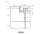
例示的な基板支持体300の特徴は、図3Aおよび図3Bにより詳細に示されている。基板支持体300は、絶縁体リングまたはプレート304と、絶縁体プレート304上に配置された(たとえば、ESCの)ベースプレート308とを含む。ベースプレート308は、処理のために上に配置された基板316を支持するように構成されたセラミック層312を支持する。図3Aにおいて、セラミック層312は、非段差状の構成を有する。図3Bにおいて、セラミック層312は、段差状の構成を有する。基板支持体300は、上部(「トップ」)エッジリング324を支持するボトムリング320を含む。1つまたは複数のビアまたはガイドチャネル328は、エッジリング324を選択的に上昇または下降させるように配置されたそれぞれのリフトピン332を収容するために、絶縁体プレート304、ボトムリング320、および/またはベースプレート308によって形成されてよい。たとえば、ガイドチャネル328は、リフトピン332のそれぞれのためのピン整列穴として機能する。図3Bに示すように、基板支持体300は、ボトムリング320とエッジリング324との間に配置されたミドルリング336をさらに含んでよい。段差状の構成では、ミドルリング336は、セラミック層312と重なり、基板316の外側エッジを支持するように配置される。 Features of
リフトピン332は、耐浸食性材料(たとえば、サファイア)を備えてよい。リフトピン332の外側面は、リフトピン332と、ボトムリング320の構造的機能との間の摩擦を減らして動きを容易にするために、滑らかに研磨されてよい。いくつかの例では、1つまたは複数のセラミックスリーブ340が、リフトピン332の周りのチャネル328に配置されてよい。リフトピン332のおのおのは、上端344とエッジリング324との間の接触面積を最小化するために、丸い上端344を含んでよい。滑らかな外側面、丸い上端344、ガイドチャネル328、および/またはセラミックスリーブ340は、エッジリング324の上昇および下降を容易とし、移動中のリフトピン332の拘束を防止する。 Lift pins 332 may comprise an erosion resistant material (eg, sapphire). The outer surface of the lift pins 332 may be smooth polished to reduce friction and facilitate movement between the lift pins 332 and the structural features of the
図3Aに示されるように、ボトムリング320は、ガイド構造348を含む。図3Bにおいてミドルリング336は、ガイド構造348を含む。たとえば、ガイド構造348は、ボトムリング320/ミドルリング336から上方に延びる上昇した環状リム352に対応する。図3Aにおいて、ガイドチャネル328およびリフトピン332は、エッジリング324と係合するためにガイド構造348を通って延びる。逆に、図3Bにおいて、ガイドチャネル328およびリフトピン332は、ボトムリング320を通って延び、ミドルリング336を通過することなくエッジリング324と係合する。 As shown in FIG. 3A,
エッジリング324は、ガイド構造348を受け入れるように配置された環状の底部溝356を含む。たとえば、エッジリング324のプロファイル(すなわち、断面)形状は、一般的に、ガイド構造348を受け入れるように構成された「U」形状に対応してよいが、他の適切な形状が使用されてよい。さらに、エッジリング324の上面は、一般的に水平(すなわち、基板支持体300の上面に平行)として示されているが、エッジリング324の上面は、他の例では異なるプロファイルを有してよい。たとえば、エッジリング324の上面は、傾斜または偏向し、丸みを帯びていてもよい。いくつかの例では、内径の侵食を補償するために、エッジリング324の内径の厚さが、エッジリング324の外径の厚さよりも大きくなるように、エッジリング324の上面が傾斜されている。
したがって、エッジリング324の底面は、図3Aのボトムリング320の上面、または、図3Bのボトムリング320およびミドルリング336のそれぞれの表面を補完するように構成される。さらに、エッジリング324とボトムリング320/ミドルリング336との間の界面360は迷路状である。言い換えれば、エッジリング324の下面と、相応して界面360とは、基板支持体300の内部構造へのエッジリング324とボトムリング320/ミドルリング336との間の直接的な(たとえば、視線)経路を提供するのではなく、むしろ多数の方向の変化(たとえば、90度の方向の変化、上方および下方への段差、水平および垂直の交互の直交経路等)を含む。典型的には、プラズマおよび処理材料の漏れの可能性は、多数の界面リング(たとえば、トップエッジリング324と、ミドルリング336およびボトムリング320のうちの1つまたは複数との両方)を含む基板支持体において高められてよい。この可能性は、可動エッジリング324が、処理中に上昇されるとさらに高められてよい。したがって、界面360(および、特に、エッジリング324のプロファイル)は、処理材料、プラズマ等が、基板支持体300の内部構造に到達することを防止するように構成される。 Accordingly, the bottom surface of
たとえば、図3Aに示すように、界面360は、ガイドチャネル328およびピン332、セラミック層312、基板316の裏側およびエッジ等へのアクセスを制限するための5つの方向の変化を含む。逆に、図3Bに示すように、界面360は、ガイドチャネル328およびピン332、セラミック層312、基板316の裏側およびエッジ、接着層372、シール376等へのアクセスを制限するために、第1の経路364に7つの方向の変化、および第2の経路368に5つの方向の変化を含む。したがって、界面360は、基板支持体300の内部構造に影響を及ぼすプラズマ漏れおよび点灯、侵食等の可能性を低下させる。 For example, as shown in FIG. 3A,
エッジリング324のプロファイル(すなわち、断面)形状(ならびに、ボトムリング320、ミドルリング336等の界面)は、製造を容易にし、製造コストを低減するように設計されている。たとえば、溝356の壁380、384およびガイド構造340は、プラズマおよび処理材料の漏れを防止しながら製造を容易にするために、(たとえば、放物線、台形、三角形等とは対照的に)実質的に垂直であってよい。単なる例として、実質的に垂直は、エッジリング324の上面および/または下面の法線の1°以内で、エッジリング324の上面および/または下面に垂直であり、エッジリング324の移動の方向に対して平行である等と定義されてよい。さらに、垂直壁380、384は、エッジリング324の移動中にガイド構造340に対するエッジリング324の整列を維持する。対照的に、溝356およびガイド構造340のそれぞれのプロファイルが放物線、台形、三角形等である場合、エッジリング324の上方への移動により、壁380と壁384との間の著しい分離を引き起こす。 The profile (ie, cross-sectional) shape of edge ring 324 (as well as the interfaces of
界面360内(および特に溝356内)のエッジリング324、ボトムリング320、およびミドルリング336の表面は、比較的滑らかで連続的であり、エッジリング324の移動中のエッジリング324とガイド構造340との間の摩擦を最小化する。所望の表面平滑性を達成するために、たとえば、界面360内のエッジリング324、ボトムリング320、およびミドルリング336のそれぞれの表面は、追加の研磨がなされてよい。他の例では、界面360内のエッジリング324、ボトムリング320、およびミドルリング336の表面は、摩擦をさらに低減する材料でコーティングされてよい。さらに他の例では、界面360内のエッジリング324、ボトムリング320、およびミドルリング336(および、特に、エッジリング324)の表面には、ネジ穴および/または同様のアセンブリ機能がない場合がある。このようにして、(たとえば、エッジリング324の移動中の)表面間の接触による粒子の生成が最小化されてよい。 The surfaces of
上述のように処理中にエッジリング324がチューニングのために上昇されると、図2Aおよび図2Bで説明されたように、コントローラ228は、ガイド構造348の高さHにしたがって、エッジリング324の調整可能な範囲を制限するように構成される。たとえば、調整可能な範囲は、ガイド構造348の高さH未満に制限されてよい。たとえば、ガイド構造348が、約0.24インチ(たとえば、0.22インチ(6.10mm)から0.26インチ(6.60mm))の高さHを有する場合、エッジリング324の調整可能な範囲は0.25インチ(6.35mm)であってよい。言い換えると、エッジリング324における溝356から、ガイド構造348を完全に除去することなく、エッジリング324は、完全に下降された位置(たとえば0.0インチ(0.0mm))から、完全に上昇した位置(たとえば0.25インチ(6.35mm))まで上昇されてよい。したがって、完全に上昇された位置であっても、エッジリング324は、ガイド構造348の少なくとも一部と依然として重なる。このようにエッジリング324の範囲の制限は、上述したような迷路状の界面360を保持し、エッジリング324の横方向の位置ずれを防止する。溝356の深さは、ガイド構造348の高さHにほぼ等しく(たとえば、5%以内)てよい。溝356の深さは、エッジリングの厚さの少なくとも50%であってよい。単なる例として、図3Aのエッジリング324の調整可能な範囲は、0.15インチ(3.81mm)から0.25インチ(6.35mm)であり、図3Bのエッジリング324の調整可能な範囲は、0.05インチ(1.3mm)から0.15インチ(3.81mm)である。たとえば、エッジリング324の厚さ(すなわち、高さ)は、約0.50インチ(12.7mm)(たとえば、0.45インチ(11.4mm)から0.55インチ(14.0mm))と、約0.6インチ(15.2mm)(たとえば、0.58インチ(14.7mm)から0.620インチ(15.75mm))との間であってよく、溝356の深さは、約0.30インチ(7.62mm)(たとえば、0.29インチ(7.37mm)から0.31インチ(7.87mm))であってよい。 When the
たとえば、本明細書で使用されるエッジリング324の「厚さ」は、エッジリング324の内径におけるエッジリング324の厚さ(たとえば、内壁388におけるエッジリング324の厚さ/高さ)を称してよい。いくつかの例では、エッジリング324の厚さは、エッジリング324の上面にわたって均一ではなくてよく(たとえば、エッジリング324の上面は、内壁388における厚さが、エッジリング324の外径の厚さより大きくなるように、上述したように傾斜されてよい)。しかしながら、プラズマへの曝露による侵食は、エッジリング324の外径に対して内壁388において増加されてよいので、内壁388において増加した侵食を補償するために、エッジリング324は、内壁388が少なくとも所定の厚さを有するように形成されてよい。単なる例として、内壁388は、エッジリング324の移動中に基板316との接触を避けるために実質的に垂直である。 For example, the “thickness” of
図4A、図4B、および図4Cを参照すると、別の例示的な基板支持体400がより詳細に示されている。基板支持体400は、絶縁体リングまたはプレート404と、絶縁体プレート404上に配置されたベースプレート408とを含む。ベースプレート408は、処理のために上に配置された基板416を支持するように構成されたセラミック層412を支持する。図4Aにおいて、セラミック層412は、非段差状の構成を有する。図4Bおよび図4Cにおいて、セラミック層412は段差状の構成を有する。基板支持体400は、上部エッジリング424を支持するボトムリング420を含む。段差状の構成では、エッジリング424は、セラミック層412と重なる。エッジリング424を選択的に上昇および下降させるように配置されたそれぞれのリフトピン432を収容するために、絶縁体プレート404、ボトムリング420、および/またはベースプレート408を介して、1つまたは複数のビアまたはガイドチャネル428が形成されてよい。たとえば、ガイドチャネル428は、リフトピン432のそれぞれのピン整列穴として機能する。 4A, 4B, and 4C, another
図4A、図4B、および図4Cの例では、エッジリング424は、セラミック層412上に配置された基板416の外側エッジを支持するように構成される。たとえば、エッジリング424の内径は、基板416の外側エッジを支持するように配置された段差434を含む。したがって、エッジリング424は、エッジリング424の取り外しおよび交換を容易にするために上昇および下降されてよいが、処理中は上昇および下降はできない(すなわち、エッジリング424は調整可能ではない)。たとえば、エッジリング424は、取り外しおよび交換のためにリフトピン432を使用して(たとえば、ロボット170を使用して)上昇されてよい。 In the example of FIGS. 4A, 4B, and 4C,
例では、基板支持体400上のエッジリング424の位置合わせ(すなわち、センタリング)を容易にするために、エッジリング424の下側の内側コーナ436が面取りされてよい。逆に、セラミック層412の上部の外側コーナ444および/または下部の内側コーナ448は、コーナ436と補完的に面取りされてよい。したがって、エッジリング424が基板支持体400上に下降されると、面取りされたコーナ436は、面取りされたコーナ444/448と相互作用して、エッジリング424を、基板支持体400上で自立させる。 In an example, a lower
エッジリング424の上部の外側コーナ456は、処理チャンバ102からのエッジリング424の取り外しを容易にするために面取りされてよい。たとえば、基板支持体400は、エッジリング424のその場での除去のために(すなわち、処理チャンバ102を完全に開放および通気することなく)構成されるため、エッジリング424は、エアロックを介して除去されるように構成される。典型的に、エアロックは、所定のサイズ(たとえば、300mm)の基板を収容できるサイズとされる。しかしながら、エッジリング424は、基板416よりも著しく大きい直径を有しており、典型的なエッジリング424は、エアロックを通って適合しない場合がある。したがって、エッジリング424の直径は(たとえば、図3Aおよび図3Bに示されるエッジリング324と比較して)低減される。たとえば、エッジリング324の外径は、ボトムリング320の外径と同等である。逆に、エッジリング424の外径は、ボトムリング420の外径よりも著しく小さい。単なる例として、エッジリング424の外径は、約13インチ(33.0cm)(たとえば、12.5インチ(31.8cm)から13インチ(33.0cm))以下である。外側コーナ456を面取りすることは、エアロックを通るエッジリング424の移動をさらに容易にする。 A top
単なる例として、外側コーナの面取りは、0.050インチ(1.27mm)から0.070インチ(1.78mm)の高さ、0.030インチ(0.76mm)から0.050インチ(1.27mm)の幅、および25から35°の角度を有してよい。いくつかの例では、下部コーナ436の面取りは、約0.025インチ(6.35mm)(たとえば、0.015インチ(0.381mm)から0.040インチ(1.02mm))の高さ、約0.015インチ(0.381mm)(たとえば、0.005インチ(0.13mm)から0.030インチ(0.76mm))の幅、および約60°(50~70°)の角度を有してよい。単なる例として、エッジリング424の厚さ(すなわち、高さ)は、約0.275インチ(6.985mm)(たとえば、0.25インチ(6.35mm)から0.30インチ(7.62mm))であるが、それを上回ることはない。たとえば、エッジリング424の厚さは、エッジリング424の除去を可能にするために、処理チャンバ102のエアロックの高さを超えないであろう。単なる例として、本明細書で使用されるエッジリング424の「厚さ」は、図3Aおよび図3Bに関して上述したように、エッジリング424の内径におけるエッジリング424の厚さ(たとえば、内壁458におけるエッジリング424の厚さ/高さ)を称してよい。 By way of example only, the outer corner chamfer may have a height of 0.050 inch (1.27 mm) to 0.070 inch (1.78 mm) and a height of 0.030 inch (0.76 mm) to 0.050 inch (1.78 mm). 27 mm) and an angle of 25 to 35°. In some examples, the
図4Cに示されるように、ボトムリング420は、ガイド構造460を含む。たとえば、ガイド構造460は、ボトムリング420から上方に延びる上昇した環状リム464に対応する。ガイドチャネル428およびリフトピン432は、ボトムリング420を通って延び、エッジリング424と係合する。エッジリング424は、ガイド構造460を受け入れるように配置された環状の底部溝468を含む。たとえば、エッジリング424のプロファイルは、一般的に、ガイド構造460を受け入れるように構成された「U」字形に対応してよい。 As shown in FIG. 4C,
したがって、図3Aおよび図3Bの例と同様に、図4Cにおけるエッジリング424の底面は、迷路状の界面472を形成するために、ボトムリング420およびセラミック層412のそれぞれの上面に補完的であるように構成される。言い換えれば、界面472は、基板支持体400の内部構造へのエッジリング424とボトムリング420との間の直接的な経路を提供するのではなく、むしろ多数の方向の変化(たとえば、90度の方向の変化)を含む。いくつかの例では、界面360内のガイド構造460、エッジリング424、ボトムリング420、および/またはセラミック層412の一部は、基板支持体400上のエッジリング424の整列(すなわち、センタリング)を容易にするために面取りされてよい。たとえば、エッジリング424の内径の下部の内側コーナ476と、セラミック層412の対応する下部の内側コーナ480および/または上部の外側コーナ484は、面取りされる。他の例では、溝468内のガイド構造460の機械的な整列が、エッジリング324を中心にする。いくつかの例では、下部コーナ476の面取りは、約0.025インチ(6.35mm)(たとえば、0.015インチ(0.381mm)から0.040インチ(1.02mm))の高さ、約0.015インチ(0.381mm)(たとえば、0.005インチ(0.13mm)から0.030インチ(0.76mm))の幅、および約60°(たとえば、50~60°)の角度を有してよい。 3A and 3B, the bottom surface of
図5Aおよび図5Bを参照すると、別の例示的な基板支持体500がより詳細に示される。基板支持体500は、絶縁体リングまたはプレート504と、絶縁体プレート504上に配置されたベースプレート508とを含む。ベースプレート508は、処理のために上に配置された基板516を支持するように構成されたセラミック層512を支持する。図5Aにおいて、セラミック層512は、非段差状の構成を有する。図5Bにおいて、セラミック層512は、段差状の構成を有する。基板支持体500は、(図5Aに示すように)上部エッジリング524または(図5Bに示すように)上部エッジリング526を支持するボトムリング520を含む。エッジリング524/526を選択的に上昇および下降させるように配置されたそれぞれのリフトピン532を収容するために、1つまたは複数のビアまたはガイドチャネル528が、絶縁体プレート504、ボトムリング520、および/またはベースプレート508を通して形成されてよい。たとえば、ガイドチャネル528は、リフトピン532のそれぞれのピン整列穴として機能する。図5Bに示すように、基板支持体500はさらに、ボトムリング520とエッジリング526との間に配置されたミドルリング536を含んでよい。段差状の構成では、ミドルリング536はセラミック層512と重なり、基板516の外側エッジを支持するように配置される。 5A and 5B, another
図5Aおよび図5Bの例は、図3Aおよび図3Bの調整可能なエッジリング324と、図4A、図4B、および図4Cの取り外し可能/交換可能なエッジリングとの両方の機能を組み合わせている。たとえば、図5Bの段差状の構成においても、エッジリング526は、基板516の下に延びず、基板516を支持しない。したがって、処理中にエッジリング524/526が上昇および下降されてよい。単なる例として、図5Aのエッジリング524の調整可能な範囲は、0.05インチ(1.3mm)から0.15インチ(3.81mm)であり、図5Bのエッジリング526の調整可能な範囲は、0.02インチ(0.51mm)から0.05インチ(1.3mm)である。さらに、エッジリング524/526の外径は、エアロックを介したエッジリング524/526の移動を容易にするために、図4A、図4B、および図4Cに関して説明したように低減される。したがって、エッジリング524/526は、上述のようにその場で取り外して交換されてよい。 The example of FIGS. 5A and 5B combines features of both the
図5Aに示されるように、ボトムリング520は、ガイド構造540を含む。図5Bにおいて、ミドルリング536は、ガイド構造540を含む。たとえば、ガイド構造540は、ボトムリング520/ミドルリング536から上方に延びる上昇した環状リム544に対応する。図5Aおよび図5Bのおのおのにおいて、ガイドチャネル528およびリフトピン532は、ボトムリング520を通って延び、エッジリング524/526と係合する。たとえば、エッジリング524/526は、ガイド構造540を受け入れるように配置された環状の底部溝548を含む。たとえば、エッジリング524/526のプロファイルは、一般的に、ガイド構造540を受け入れるように構成された「U」字形に対応してよい。 As shown in FIG. 5A,
したがって、図3A、図3B、および図4Cと同様に、エッジリング524/526の底面は、ボトムリング520およびミドルリング536のそれぞれの上面に補完的であるように構成され、迷路状の界面552を形成する。言い換えれば、界面552は、基板支持体500の内部構造へのエッジリング524/526とボトムリング520との間の直接的な経路を提供するのではなく、むしろ多数の方向の変化(たとえば、90度の方向の変化)を含む。いくつかの例では、界面552内のガイド構造540、エッジリング524/526、ボトムリング520、および/またはミドルリング536の一部は、基板支持体500上のエッジリング524/526の整列(すなわち、センタリング)を容易にするために面取りされてよい。たとえば、図5Aにおいて、エッジリング524のコーナ556、558と、ボトムリング520のガイド構造540、562の補完的なコーナ560とが面取りされている。逆に、図5Bにおいて、エッジリング526のコーナ556と、ボトムリング520のコーナ560のみが面取りされている。エッジリング524の上部の外側コーナ564は、図4A、図4B、および図4Cに関して上述したように、処理チャンバ102からのエッジリング524の取り外しを容易にするために面取りされてよい。 3A, 3B, and 4C, the bottom surfaces of edge rings 524/526 are configured to be complementary to the top surfaces of
単なる例として、下部コーナ556、558の面取りは、約0.005インチ(0.13mm)から0.030インチ(0.76mm)の高さおよび幅、ならびに約25から35°の角度を有してよい。たとえば、エッジリング524/526の厚さ(すなわち、高さ)は、約0.25インチ(6.35mm)(たとえば、0.25インチ(6.35mm)から0.26インチ(6.60mm))以下であり、溝548の深さは、0.200インチ(5.08mm)から0.220インチ(6.096mm)であってよい。エッジリング524/526の厚さと、溝548の深さとの差は、0.075インチ(1.91mm)以上であってよい。たとえば、エッジリング524/526の厚さは、エッジリング524/526の除去を可能にするために、処理チャンバ102のエアロックの高さを超えない。しかしながら、エッジリング524/526の調整可能性を最適化するために、エアロックの高さを超えることなく、エッジリング524/526の厚さが最大化されてよい。言い換えれば、エッジリング524/526が時間とともに侵食されると、交換する必要なくエッジリング524/526が上昇されてよい量は、エッジリング524/526の厚さに比例して増加する。単なる例として、本明細書で使用されるエッジリング524/526の「厚さ」は、図3A、図3B、図4A、図4B、および図4Cに関して上述したように、エッジリング524/526の内径におけるエッジリング524/526の厚さ(たとえば、内壁568におけるエッジリング524/526の厚さ/高さ)を称してよい。 Merely by way of example, the chamfers of the
図6Aおよび図6Bを参照すると、(たとえば、ボトムリング320、420、または520のいずれかに対応する)例示的なボトムリング600は、ボトムリング600の絶縁体リング604との位置合わせを容易にするために、クロッキング機能を実装してよい。ボトムリング600は、絶縁体リング604を通って延びるそれぞれのリフトピン612を受け入れるように配置された複数のガイドチャネル608を含む。ボトムリング600はさらに、ノッチ616のような1つまたは複数のクロッキング機能を含む。ノッチ616は、絶縁体リング604から上方に延びる突起620のような補完的な構造を受け入れるように構成される。したがって、ボトムリング600は、ガイドチャネル608がリフトピン612のそれぞれと確実に整列するように、ノッチ616が突起620と整列し、突起620を受け入れるように設置されてよい。 6A and 6B, an exemplary bottom ring 600 (e.g., corresponding to any of bottom rings 320, 420, or 520) facilitates alignment of
図7A、図7B、および図7Cを参照すると、基板支持体700は、本開示の原理にしたがって、非段差状の構成でトップ可動エッジリングを支持するように構成された例示的なボトムリング704、708、712を含む。たとえば、図7Aに示されるように、ボトムリング704は、図3Aのエッジリング324を支持するように構成される。図7Bに示されるように、ボトムリング708は、図4Aのエッジリング424を支持するように構成される。図7Cに示されるように、ボトムリング712は、図5Aのエッジリング524を支持するように構成される。ボトムリング704、708、712のおのおののそれぞれの上面は段差状である。言い換えれば、それぞれの上面のおのおのは、少なくとも2つの異なる高さを有する。 7A, 7B, and 7C,
基板支持体700は、絶縁体リングまたはプレート716と、絶縁体プレート716上に配置された(たとえば、ESCの)ベースプレート720とを含む。ベースプレート720は、処理のために上の基板を支持するように構成されたセラミック層724を支持する。それぞれのエッジリングを選択的に上昇および下降させるように配置されたリフトピン732を収容するために、絶縁体プレート716およびボトムリング704、708、712を介して1つまたは複数のビアまたはガイドチャネル728が形成されてよい。たとえば、ガイドチャネル728は、リフトピン732のそれぞれのピン整列穴として機能する。リフトピン732と、ガイドチャネル728の内側面との間のギャップは、プラズマ漏れを低減するために、最小化される。言い換えれば、ガイドチャネル728の直径は、リフトピン732の直径よりもわずかに大きい(たとえば、0.005インチ(0.13mm)~0.010インチ(0.254mm)大きい)だけである。たとえば、リフトピン732は、0.057インチ(1.45mm)~0.061インチ(1.55mm)の直径を有してよく、ガイドチャネル728は、0.063インチ(1.60mm)~0.067インチ(1.70mm)の直径を有してよい。いくつかの例では、ガイドチャネル728は、プラズマ漏れをさらに制限するために、ガイドチャネル728の他の部分よりも小さい直径を有する狭い領域734を含む。たとえば、狭い領域734は、ガイドチャネル728の直径よりも0.002~0.004インチ(0.051~0.102mm)小さい直径を有してよい。同様に、いくつかの例では、リフトピン732は、ガイドチャネル728の狭い領域734内に位置する狭い領域を含んでよい。
図7Aに示されるように、ボトムリング704は、ガイド構造736を含む。たとえば、ガイド構造736は、ボトムリング704から上方に延びる上昇した環状リム740に対応する。リム740および内側環状リム742は、溝744を画定する。ガイドチャネル728およびリフトピン732は、ガイド構造736を通って延びる。ボトムリング704の上面は、エッジリング324の底面に対して補完的であるように構成され、上述のような方向の複数の変化を含む迷路状の界面を形成する。溝744およびリム740のそれぞれの幅は、溝744およびリム740のそれぞれの垂直面と、エッジリング324の底部における補完的な垂直面との間のギャップを最小化するように選択される。たとえば、ギャップは0.02インチ(0.51mm)未満であってよい。 As shown in FIG. 7A,
同様に、図7Cに示されるように、ボトムリング712は、ガイド構造746を含む。たとえば、ガイド構造746は、ボトムリング712から上方に延びる上昇した環状リム748に対応する。リム748および内側環状リム750は、第1の溝752を画定し、リム748および外側環状リム754は、第2の溝756を画定する。ガイドチャネル728およびリフトピン732は、ボトムリング712を通って延びる。ボトムリング712の上面は、上記のような方向の複数回変化を含む迷路状の界面を形成するために、エッジリング524の底面に対して補完的であるように構成される。リム748の高さは、内側環状リム750とエッジリング524との間の接触前に、リム748のエッジリング524との係合を容易にするために、内側環状リム750の高さよりも大きい。 Similarly,
いくつかの例では、ガイド構造746および/またはボトムリング712の一部は、基板支持体700上のエッジリング524の位置合わせ(すなわち、センタリング)を容易にするために面取りされてよい。たとえば、ガイド構造746のコーナ760、764とボトムリング712のコーナ768とが、面取りされる。いくつかの例では、コーナ760の面取りは、少なくとも約0.008インチ(0.20mm)(たとえば、0.007インチ(0.18mm)から0.011インチ(0.279mm))の高さおよび幅、ならびに15~25°の角度を有してよい。コーナ764の面取りは、少なくとも約0.01インチ(0.25mm)(たとえば、0.01インチ(0.25mm)から0.02インチ(0.51mm))の高さおよび幅と、20~35°の角度を有してよい。コーナ768の面取りは、少なくとも約0.010インチ(0.254mm)(たとえば、0.010インチ(0.254mm)から0.030インチ(0.76mm))の高さおよび幅、ならびに20~35°の角度を有してよい。 In some examples,
ボトムリング704、708、712の内径は、少なくとも11.5インチ(29.21cm)(たとえば、11.5インチ(29.21cm)と11.7インチ(29.72cm)との間)であってよい。ボトムリング704、708、712の外径は、14インチ(35.6cm)以下(たとえば、13.8インチ(35.05cm)と14.1インチ(35.81cm)の間)であってよい。772におけるボトムリング708、712の段差内径は、エッジリング424または524の外径を収容するように選択される。たとえば、エッジリング424または524の外径は、約12.8インチ(32.51cm)(たとえば、+/-0.10インチ(2.54mm))であってよい。したがって、772におけるボトムリング708、712の内径は、少なくとも13.0インチ(33.02cm)であってよい。 The inner diameter of the bottom rings 704, 708, 712 is at least 11.5 inches (29.21 cm) (eg, between 11.5 inches (29.21 cm) and 11.7 inches (29.72 cm)); good. The outer diameter of the bottom rings 704, 708, 712 may be 14 inches (35.6 cm) or less (eg, between 13.8 inches (35.05 cm) and 14.1 inches (35.81 cm)). The stepped inner diameter of bottom rings 708 , 712 at 772 is selected to accommodate the outer diameter of
図8A、図8B、および図8Cを参照すると、基板支持体800は、本開示の原理による段差状の構成でトップ可動エッジリングを支持するように構成された例示的なボトムリング804、808、812を含む。たとえば、図8Aに示されるように、ボトムリング804は、図3Bのエッジリング324を支持するように構成される。図8Bに示されるように、ボトムリング808は、図4Cのエッジリング424を支持するように構成される。図8Cに示されるように、ボトムリング812は、図5Bのエッジリング526を支持するように構成される。ボトムリング804、812はさらに、図3Bのミドルリング336と、図5Bのミドルリング536とをそれぞれ支持するように構成されてよい。ボトムリング804、808、812のおのおののそれぞれの上面は、段差状である。言い換えれば、それぞれの上面のおのおのは、少なくとも2つの異なる高さを有する。 8A, 8B, and 8C,
基板支持体800は、絶縁体リングまたはプレート816と、絶縁体プレート816上に配置された(たとえば、ESCの)ベースプレート820とを含む。ベースプレート820は、処理のために上の基板を支持するように構成されたセラミック層824を支持する。接着層828は、ベースプレート820とセラミック層824との間に配置されてよく、シール832は、接着層828を囲む。それぞれのエッジリングを選択的に上昇および下降させるように配置されたリフトピン840を収容するために、絶縁体プレート816およびボトムリング804、808、812を介して、1つまたは複数のビアまたはガイドチャネル836が形成されてよい。たとえば、ガイドチャネル836は、リフトピン840のそれぞれのピン整列穴として機能する。リフトピン840とガイドチャネル836の内側面との間のギャップは、プラズマ漏れを低減するために、最小化される。言い換えれば、ガイドチャネル836の直径は、リフトピン840の直径よりもわずかに大きい(たとえば、0.005インチ(0.13mm)~0.010インチ(0.254mm)大きい)だけである。たとえば、リフトピン840は0.1インチ(2.5mm)の直径を有してよい一方、ガイドチャネル836は0.105インチ(2.667mm)の直径を有する。いくつかの例では、ガイドチャネル836は、プラズマ漏れをさらに制限するために、ガイドチャネル836の他の部分よりも小さい直径を有する狭い領域842を含む。たとえば、狭い領域842は、ガイドチャネル836の直径よりも0.002~0.004インチ(0.051~0.10mm)小さい直径を有してよい。いくつかの例では、1つまたは複数のセラミックスリーブ844が、リフトピン840の周りのチャネル836に配置されてよい。
図8Bに示されるように、ボトムリング808は、ガイド構造846を含む。たとえば、ガイド構造846は、ボトムリング808から上方に延びる上昇した環状リム848に対応する。リム848および外側環状リム850は、溝852を画定する。ボトムリング808の上面は、上述のような方向の複数変化を含む迷路状の界面を形成するために、エッジリング424の底面に対して補完的であるように構成される。溝852およびリム848のそれぞれの幅は、溝852およびリム848のそれぞれの垂直面と、エッジリング424の底部における補完的な垂直面との間のギャップを最小化するように選択される。たとえば、ギャップは、0.010インチ(0.254mm)未満であってよい。逆に、図8Aおよび図8Cにおいて、ボトムリング804、812は、それぞれのガイド構造348、540を有するミドルリング336、536を支持するように構成される。したがって、ボトムリング804、812の上面は、上述したように、方向の複数変化を含む迷路状の界面を形成するために、ミドルリング336、536の上面と組み合わされて、エッジリング324、526の底面に補完的になるように構成される。 As shown in FIG. 8B,
ガイドチャネル836がセラミックスリーブ844を含む例(たとえば、ガイドチャネル836が、ベースプレート820を通ってルーティングされる例)では、ボトムリング804、808、812は、セラミックスリーブ844を収容するように構成されてよい。たとえば、ボトムリング804、808、812は、セラミックスリーブ844の上端を収容するために、ガイドチャネル836よりも大きな直径を有するキャビティまたは切り欠き856のようなクリアランス機能を含んでよい。いくつかの例では、ボトムリング804、808、812は、リフトピン840に続いて設置されてよい。したがって、ボトムリング804、808、812におけるそれぞれの開口部は、リフトピン840上方へのボトムリング804、808、812の設置を容易にするために面取りされたエッジ860を含んでよい。たとえば、エッジ860の面取りは、0.020インチ(0.508mm)から0.035インチ(0.889mm)の高さおよび幅、ならびに40~50°の角度を有してよい。 In examples in which guide
図8Bおよび図8Cに図示されるように、862におけるボトムリング808、812の段差内径は、図4Cのエッジリング424および図5Bのエッジリング526の外径を収容するように選択される。たとえば、エッジリング424、526の外径は、約12.8インチ(32.51cm)(たとえば、+/-0.10インチ(2.54mm))であってよい。したがって、862におけるボトムリング808、812の内径は、少なくとも13.0インチ(33.02cm)であってよい。したがって、ボトムリング808、812とエッジリング424、526との垂直面間の接触をなお防止しながら、ボトムリング808、812とエッジリング424、526の外径との間のギャップを最小化することができる。 As illustrated in FIGS. 8B and 8C, the stepped inner diameter of bottom rings 808, 812 at 862 is selected to accommodate the outer diameter of
いくつかの例では、図8Bに示されるように、ボトムリング808は、864における第1の外径、および868における第2の外径を含んでよい。第2の外径868は、864における第1の外径よりも大きい。たとえば、基板支持体800は、絶縁体プレート816、ベースプレート820、ボトムリング808等の外側部分を保護するライナ872を含んでよい。しかしながら、ライナ872は、プラズマに曝されるボトムリング808の上部を保護しない場合があり、(破線矢印880で示すように)ベースプレート820の上部エッジ876に隣接する領域におけるボトムリング808の増加した浸食が発生する可能性があってよい。したがって、ボトムリング808は、増加した侵食を補償するために、第2の外径868に追加の材料を含む。 In some examples,
図9を参照すると、例示的なミドルリング900が示されている。ミドルリング900は、トップエッジリングが別の方法で基板支持体の2つの異なる構成要素の上面によって支持される構成で提供されてよい。たとえば、図3Bおよび図5B(それぞれ図8Aおよび図8Cに対応する)に示されるように、トップエッジリングは、それぞれのセラミック層およびそれぞれのボトムリングの両方と重なる。したがって、ミドルリング900は、別の方法ではセラミック層によって支持されるトップエッジリングの一部を支持するように配置される。示されるように、ミドルリング900は「U」字形である。 Referring to FIG. 9, an exemplary
ミドルリング900は、溝912を画定する内側環状リム904および外側環状リム908を含む。溝912は、それぞれのトップエッジリング(たとえば、エッジリング324または526)を受け入れるように構成される。反対に、外側環状リム908は、図3Bおよび図5Bで上述したように、交換中にトップエッジリング324または526を中心に置くためのガイド構造として機能する。いくつかの例では、コーナ916、920は、トップエッジリングとの係合を容易にするために面取りされる。たとえば、コーナ916の面取りは、少なくとも約0.010インチ(0.254mm)(たとえば、0.005インチ(0.13mm)から0.015インチ(0.381mm))の高さおよび幅と、約20°(たとえば、15~25°)の角度とを有してよい。コーナ920の面取りは、少なくとも約0.015インチ(0.381mm)(たとえば、0.010インチ(0.254mm)から0.020インチ(0.508mm))の高さおよび幅と、約30°(たとえば、25~35°)の角度とを有してよい。外側環状リム908の幅は、リム908のそれぞれの垂直面と、エッジリング324または526の底部の補完的な垂直面との間のギャップを最小化するように選択される。たとえば、ギャップは、プラズマ漏れを制限するために0.010インチ(0.254mm)未満であってよい。
図10Aおよび図10Bを参照すると、基板支持体1000の2つの断面図は、本開示の原理にしたがって、段差状の構成で、トップ可動エッジリングを支持するように構成されたボトムリング1004を示す。たとえば、ボトムリング1004は、図5Bおよび図8Cに示されるものと同様の構成でエッジリング(たとえば、526)を支持するように構成される。ボトムリング1004はさらに、図5Bに示されるものと同様の構成でミドルリングを支持するように構成されてよい。 10A and 10B, two cross-sectional views of
基板支持体1000は、絶縁体リングまたはプレート1008と、絶縁体プレート1008上に配置された(たとえば、ESCの)ベースプレート1012とを含む。ベースプレート1012は、処理のために上の基板を支持するように構成されたセラミック層1016を支持する。接着層1020は、ベースプレート1012とセラミック層1016との間に配置されてよく、シール1024が接着層1020を囲んでいる。図10Aに示されるように、エッジリングを選択的に上昇および下降させるために配置されたリフトピン1032を収容するために、1つまたは複数のビアまたはガイドチャネル1028が、絶縁体プレート1008、ベースプレート1012、およびボトムリング1004を通して形成されてよい。たとえば、ガイドチャネル1028は、リフトピン1032のそれぞれのピン整列穴として機能する。リフトピン1032と、ガイドチャネル1028の内側面との間のギャップは、プラズマ漏れを低減するために、最小化される。言い換えれば、ガイドチャネル1028の直径は、リフトピン1032の直径よりもわずかに大きい(たとえば、0.005インチ(0.13mm)~0.010インチ(0.254mm)大きい)だけである。たとえば、リフトピン1032は、0.1インチ(2.5mm)の直径を有してよく、ガイドチャネル1028は0.105インチ(2.667mm)の直径を有する。いくつかの例では、ガイドチャネル1028は、プラズマ漏れをさらに制限するために、ガイドチャネル1028の他の部分よりも小さい直径を有する狭い領域1036を含む。たとえば、狭い領域1036は、ガイドチャネル1028の直径よりも0.002~0.004インチ(0.051~0.102mm)小さい直径を有してよい。いくつかの例では、1つまたは複数のセラミックスリーブ1040が、リフトピン1032の周りのチャネル1028に配置されてよい。
基板支持体1000は、絶縁体プレート1008、ベースプレート1012、およびボトムリング1004のような基板支持体1000の構成要素を囲み保護するように配置されたライナ1044を含んでよい。図10Aおよび図10Bに示されるようなボトムリング1004は、ライナ1044上のボトムリング1004から半径方向外側に延びる環状リップ1048を含む。リップ1048は、ライナ1044が存在する場合、ボトムリング1004の取り付けおよび取り外しを容易にする。
図10Bに示されるように、ベースプレート1012は、それぞれのボルト取り付け穴1056を介して挿入されたボルト1052を使用して絶縁体プレート1008に結合されてよい。ボルト取り付け穴1056内およびボトムリング1004とベースプレート1012との間のプラズマ漏れを防止するために、セラミックプラグ1060が、ボルト1052の上方に配置される。図10Bに示されているボトムリング1004は、セラミックプラグ1060を収容するためにキャビティまたは切り欠き1064のようなクリアランス機能を含む。 As shown in FIG. 10B,
前述した説明は、本質的に単なる例示であり、開示、その適用、または使用を限定することは決して意図されていない。本開示の広範な教示は、様々な形態で実施されてよい。したがって、本開示は特定の例を含むが、本開示の真の範囲はそのように限定されるべきではない。なぜなら、図面、明細書、および添付の特許請求の範囲を検討すると他の修正が明らかになるからである。方法内の1つまたは複数のステップは、本開示の原理を変更することなく、異なる順序で(または同時に)実行されてよいことを理解されたい。さらに、特定の機能を有するものとして実施形態のおのおのが上記で説明されたが、本開示の任意の実施形態に関して説明されたこれらの特徴の1つまたは複数は、たとえその組合せが明示的に説明されていなくても、他の実施形態のいずれかの特徴で実施および/または組み合わされてよい。言い換えれば、説明された実施形態は相互に排他的ではなく、1つまたは複数の実施形態の相互の置換が、本開示の範囲内に留まる。 The foregoing description is merely exemplary in nature and is in no way intended to limit the disclosure, its application, or uses. The broad teachings of this disclosure may be embodied in various forms. Therefore, although this disclosure includes specific examples, the true scope of this disclosure should not be so limited. For other modifications will become apparent upon inspection of the drawings, specification and appended claims. It should be understood that one or more steps within a method may be performed in a different order (or concurrently) without altering the principles of the present disclosure. Furthermore, although each of the embodiments has been described above as having a particular functionality, one or more of these features described with respect to any embodiment of the disclosure may be omitted even if the combination is expressly described. Even if not, the features of any of the other embodiments may be implemented and/or combined. In other words, the described embodiments are not mutually exclusive and mutual permutations of one or more embodiments remain within the scope of the disclosure.
要素間(たとえば、モジュール、回路要素、半導体層等の間)の空間的および機能的関係は、「接続された」、「係合された」、「結合された」、「隣接する」、「次の」、「の先頭」、「上側」、「下側」、および「配置された」を含む様々な用語を使用して説明される。「直接的」であると明示的に記載されていない限り、上記の開示で第1の要素と第2の要素との関係が説明されている場合、この関係は、第1の要素と第2の要素との間に他の介在要素が存在しない直接的な関係である場合があってよいが、第1の要素と第2の要素との間に1つまたは複数の介在要素が(空間的または機能的に)存在する間接的な関係であってもよい。本明細書で使用される場合、A、B、およびCの少なくとも1つという句は、非排他的な論理的ORを使用する論理(A OR B OR C)を意味すると解釈されるべきであり、「Aのうちの少なくとも1つ、Bのうちの少なくとも1つ、および、Cのうちの少なくとも1つ」を意味すると解釈されるべきではない。 Spatial and functional relationships between elements (e.g., between modules, circuit elements, semiconductor layers, etc.) are defined as "connected", "engaged", "coupled", "adjacent", " Various terms are used to describe, including "next", "beginning of", "above", "below", and "positioned". Unless expressly stated to be "directly," when the above disclosure describes a relationship between a first element and a second element, this relationship refers to the first element and the second element. There may be cases where there is a direct relationship with no other intervening elements between the first element and the second element, but one or more intervening elements (spatial or functionally) existing indirect relationship. As used herein, the phrase at least one of A, B, and C should be interpreted to mean logic using non-exclusive logical OR (A OR B OR C). , to mean “at least one of A, at least one of B, and at least one of C”.
いくつかの実施では、コントローラは、システムの一部であり、これは上記の例の一部であってよい。そのようなシステムは、1つまたは複数の処理ツール、1つまたは複数のチャンバ、処理のための1つまたは複数のプラットフォーム、および/または特定の処理構成要素(ウェーハペデスタル、ガスフローシステム等)を含む半導体処理機器を備えてよい。これらのシステムは、半導体ウェーハまたは基板の処理前、処理中、処理後の動作を制御するための電子機器と統合されてよい。電子機器は、「コントローラ」と称されてよく、1つまたは複数のシステムの様々な構成要素またはサブパートを制御してよい。コントローラは、処理要件および/またはシステムのタイプに応じて、処理ガスの供給、温度設定(たとえば、加熱および/または冷却)、圧力設定、真空設定、電力設定、無線周波数(RF)発生器設定、RFマッチング回路設定、周波数設定、流量設定、流体供給設定、位置および動作設定、ツールおよび他の移送ツールへの、およびこれらからのウェーハの移送、および/または、特定のシステムに接続または接するロードロックを含む、本明細書で開示する処理のいずれかを制御するようにプログラムされてよい。 In some implementations, the controller is part of the system, which may be part of the examples above. Such systems may include one or more processing tools, one or more chambers, one or more platforms for processing, and/or certain processing components (wafer pedestals, gas flow systems, etc.). may be provided with semiconductor processing equipment including: These systems may be integrated with electronics for controlling pre-, during-, and post-processing operations of semiconductor wafers or substrates. The electronics may be referred to as "controllers" and may control various components or sub-parts of one or more systems. Depending on the process requirements and/or type of system, the controller provides process gas supply, temperature settings (e.g., heating and/or cooling), pressure settings, vacuum settings, power settings, radio frequency (RF) generator settings, RF matching circuit settings, frequency settings, flow rate settings, fluid supply settings, position and motion settings, transfer of wafers to and from tools and other transfer tools, and/or load locks connected to or contacting specific systems. may be programmed to control any of the processes disclosed herein, including
概して、コントローラは、命令を受信し、命令を発行し、動作を制御し、クリーニング動作を有効にし、エンドポイント測定を有効にする等、様々な集積回路、ロジック、メモリ、および/またはソフトウェアを有する電子機器として定義されてよい。集積回路は、プログラム命令を記憶したファームウェアの形式のチップ、デジタル信号プロセッサ(DSP)、特定用途向け集積回路(ASIC)として定義されたチップ、および/または、1つまたは複数のマイクロプロセッサ、またはプログラム命令(たとえば、ソフトウェア)を実行するマイクロプロセッサを含んでよい。プログラム命令は、半導体ウェーハ上または半導体ウェーハのため、または、システムへの特定の処理を実行するための動作パラメータを定義する様々な個別設定(またはプログラムファイル)の形式でコントローラに通信される命令であってよい。いくつかの実施形態では、動作パラメータは、1つまたは複数の層、材料、金属、酸化物、ケイ素、二酸化ケイ素、表面、回路、および/または、ウェーハのダイの製造中に、1つまたは複数の処理ステップを達成するために処理エンジニアによって定義されるレシピの一部であってよい。 Generally, the controller has various integrated circuits, logic, memory, and/or software to receive instructions, issue instructions, control operations, enable cleaning operations, enable endpoint measurements, etc. It may be defined as an electronic device. An integrated circuit may be a chip in the form of firmware storing program instructions, a digital signal processor (DSP), a chip defined as an application specific integrated circuit (ASIC), and/or one or more microprocessors or programs. It may include a microprocessor that executes instructions (eg, software). Program instructions are instructions communicated to the controller in the form of various settings (or program files) that define operating parameters on or for a semiconductor wafer or for performing a particular process to the system. It's okay. In some embodiments, the operating parameter is one or more of one or more layers, materials, metals, oxides, silicon, silicon dioxide, surfaces, circuits, and/or during die fabrication of a wafer. may be part of a recipe defined by the process engineer to accomplish the process steps of
いくつかの実施では、コントローラは、システムに統合された、システムに結合された、さもなければシステムにネットワーク化された、またはこれらの組合せであるコンピュータの一部であってよいか、またはこのようなコンピュータに結合されてよい。たとえば、コントローラは、「クラウド」または工場ホストコンピューターシステムのすべてまたは一部にあってもよく、これによりウェーハ処理の遠隔アクセスが可能であってよい。コンピュータは、現在の処理のパラメータを変更し、現在の処理をフォローする処理ステップを設定し、または、新たな処理を開始するために、システムへの遠隔アクセスを可能にして、製造動作の現在の進行状況を監視し、過去の製造動作の履歴を調べ、複数の製造動作から、傾向または性能指標を調べてよい。いくつかの例では、遠隔コンピュータ(たとえば、サーバ)は、ローカルネットワークまたはインターネットを含んでよいネットワークを介してシステムに処理レシピを提供してよい。遠隔コンピュータは、その後遠隔コンピュータからシステムに通信されるパラメータおよび/または設定の入力またはプログラミングを可能にするユーザインターフェースを含んでよい。いくつかの例では、コントローラは、データの形式で命令を受信する。この命令は、1つまたは複数の動作中に実行されるべき処理ステップのおのおののパラメータを指定する。パラメータは、実行されるべき処理のタイプと、コントローラがインターフェースまたは制御するように構成されているツールのタイプに固有のものであってよいことを理解されたい。したがって、上記のように、コントローラは、ともにネットワーク化され、本明細書で説明される処理および制御のような共通の目的に向かって動作する1つまたは複数の別個のコントローラを備えること等により分散されてよい。このような目的のための分散コントローラの例は、チャンバにおける処理を制御するために組み合わされる、(プラットフォームレベルにおけるような、または遠隔コンピュータの一部として)遠隔に配置された1つまたは複数の集積回路と通信するチャンバ上の1つまたは複数の集積回路であってよい。 In some implementations, the controller may be part of a computer that is integrated into the system, coupled to the system, otherwise networked to the system, or combinations thereof, or such computer. For example, the controller may reside in all or part of a "cloud" or factory host computer system, which may allow remote access for wafer processing. The computer enables remote access to the system to change the parameters of the current process, set process steps to follow the current process, or initiate a new process, thereby determining the current status of the manufacturing operation. Progress may be monitored, history of past manufacturing operations may be examined, and trends or performance indicators may be examined from multiple manufacturing operations. In some examples, a remote computer (eg, server) may provide processing recipes to the system over a network that may include a local network or the Internet. The remote computer may include a user interface that allows entry or programming of parameters and/or settings that are then communicated from the remote computer to the system. In some examples, the controller receives instructions in the form of data. The instructions specify parameters for each of the processing steps to be performed during one or more operations. It should be appreciated that the parameters may be specific to the type of processing to be performed and the type of tool that the controller is configured to interface with or control. Thus, as noted above, the controllers may be networked together and distributed, such as by having one or more separate controllers working toward a common purpose, such as the processing and control described herein. may be An example of a distributed controller for such purposes is one or more remotely located integrations (such as at the platform level or as part of a remote computer) combined to control processing in the chamber. There may be one or more integrated circuits on the chamber that communicate with the circuitry.
限定することなく、例示的なシステムは、プラズマエッチングチャンバまたはモジュール、堆積チャンバまたはモジュール、スピンリンスチャンバまたはモジュール、金属めっきチャンバまたはモジュール、クリーンチャンバまたはモジュール、ベベルエッジエッチングチャンバまたはモジュール、物理蒸着(PVD)チャンバまたはモジュール、化学蒸着(CVD)チャンバまたはモジュール、原子層蒸着(ALD)チャンバまたはモジュール、原子層エッチング(ALE)チャンバまたはモジュール、イオン注入チャンバまたはモジュール、トラックチャンバまたはモジュール、および半導体ウェーハの製造および/または製作に関連付けられてよい、または使用されてよい他の任意の半導体処理システムを含んでよい。 Without limitation, exemplary systems include plasma etch chambers or modules, deposition chambers or modules, spin rinse chambers or modules, metal plating chambers or modules, clean chambers or modules, bevel edge etch chambers or modules, physical vapor deposition (PVD ) chambers or modules, chemical vapor deposition (CVD) chambers or modules, atomic layer deposition (ALD) chambers or modules, atomic layer etch (ALE) chambers or modules, ion implantation chambers or modules, track chambers or modules, and semiconductor wafer fabrication and/or any other semiconductor processing system that may be associated with or used in fabrication.
上述のように、ツールによって実行されるべき処理ステップに応じて、コントローラは、他のツール回路またはモジュール、他のツール構成要素、クラスタツール、他のツールインターフェース、隣接ツール、近隣ツール、工場全体に配置されたツール、メインコンピュータ、別のコントローラ、または半導体製造工場内のツール場所および/またはロードポートとの間でウェーハのコンテナをやり取りする材料搬送で使用されるツールのうちの1つまたは複数と通信してよい。 As noted above, depending on the processing steps to be performed by the tool, the controller may be directed to other tool circuits or modules, other tool components, cluster tools, other tool interfaces, neighboring tools, neighboring tools, the entire factory. With one or more of the tools used in material handling to move containers of wafers to and from tool locations and/or load ports in a semiconductor fab located on a tool, a main computer, another controller, or You can communicate.
前述した説明は、本質的に単なる例示であり、開示、その適用、または使用を限定することは決して意図されていない。本開示の広範な教示は、様々な形態で実施されてよい。したがって、本開示は特定の例を含むが、本開示の真の範囲はそのように限定されるべきではない。なぜなら、図面、明細書、および以下の特許請求の範囲を検討すると他の修正が明らかになるからである。方法内の1つまたは複数のステップは、本開示の原理を変更することなく、異なる順序で(または同時に)実行されてよいことを理解されたい。さらに、特定の機能を有するものとして実施形態のおのおのが上記で説明されたが、本開示の任意の実施形態に関して説明されたこれらの特徴の任意の1つまたは複数は、たとえその組合せが明示的に説明されていなくても、他の実施形態のいずれかの特徴で実施および/または組み合わされてよい。言い換えれば、説明された実施形態は相互に排他的ではなく、1つまたは複数の実施形態の相互の置換が、本開示の範囲内に留まる。 The foregoing description is merely exemplary in nature and is in no way intended to limit the disclosure, its application, or uses. The broad teachings of this disclosure may be embodied in various forms. Therefore, although this disclosure includes specific examples, the true scope of this disclosure should not be so limited. For other modifications will become apparent upon inspection of the drawings, specification and claims that follow. It should be understood that one or more steps within a method may be performed in a different order (or concurrently) without altering the principles of the present disclosure. Furthermore, although each of the embodiments has been described above as having a particular functionality, any one or more of these features described with respect to any embodiment of the disclosure may be omitted even if the combination expressly may be implemented and/or combined with features of any of the other embodiments, even if not described. In other words, the described embodiments are not mutually exclusive and mutual permutations of one or more embodiments remain within the scope of the disclosure.
要素間(たとえば、モジュール、回路要素、半導体層等の間)の空間的および機能的関係は、「接続された」、「係合された」、「結合された」、「隣接する」、「次の」、「の先頭」、「上側」、「下側」、および「配置された」を含む様々な用語を使用して説明される。「直接的」であると明示的に記載されていない限り、上記の開示で第1の要素と第2の要素との関係が説明されている場合、この関係は、第1の要素と第2の要素との間に他の介在要素が存在しない直接的な関係である場合があってよいが、第1の要素と第2の要素との間に1つまたは複数の介在要素が(空間的または機能的に)存在する間接的な関係であってもよい。本明細書で使用される場合、A、B、およびCの少なくとも1つという句は、非排他的な論理的ORを使用する論理(A OR B OR C)を意味すると解釈されるべきであり、「Aのうちの少なくとも1つ、Bのうちの少なくとも1つ、および、Cのうちの少なくとも1つ」を意味すると解釈されるべきではない。 Spatial and functional relationships between elements (e.g., between modules, circuit elements, semiconductor layers, etc.) are defined as "connected", "engaged", "coupled", "adjacent", " Various terms are used to describe, including "next", "beginning of", "above", "below", and "positioned". Unless expressly stated to be "directly," when the above disclosure describes a relationship between a first element and a second element, this relationship refers to the first element and the second element. There may be cases where there is a direct relationship with no other intervening elements between the first element and the second element, but one or more intervening elements (spatial or functionally) existing indirect relationship. As used herein, the phrase at least one of A, B, and C should be interpreted to mean logic using non-exclusive logical OR (A OR B OR C). , to mean “at least one of A, at least one of B, and at least one of C”.
いくつかの実施では、コントローラは、システムの一部であり、これは上記の例の一部であってよい。そのようなシステムは、1つまたは複数の処理ツール、1つまたは複数のチャンバ、処理のための1つまたは複数のプラットフォーム、および/または特定の処理構成要素(ウェーハペデスタル、ガスフローシステム等)を含む半導体処理機器を備えてよい。これらのシステムは、半導体ウェーハまたは基板の処理前、処理中、処理後の動作を制御するための電子機器と統合されてよい。電子機器は、「コントローラ」と称されてよく、1つまたは複数のシステムの様々な構成要素またはサブパートを制御してよい。コントローラは、処理要件および/またはシステムのタイプに応じて、処理ガスの供給、温度設定(たとえば、加熱および/または冷却)、圧力設定、真空設定、電力設定、無線周波数(RF)発生器設定、RFマッチング回路設定、周波数設定、流量設定、流体供給設定、位置および動作設定、ツールおよび他の移送ツールへの、およびこれらからのウェーハの移送、および/または、特定のシステムに接続または接するロードロックを含む、本明細書で開示する処理のいずれかを制御するようにプログラムされてよい。 In some implementations, the controller is part of the system, which may be part of the examples above. Such systems may include one or more processing tools, one or more chambers, one or more platforms for processing, and/or certain processing components (wafer pedestals, gas flow systems, etc.). may be provided with semiconductor processing equipment including: These systems may be integrated with electronics for controlling pre-, during-, and post-processing operations of semiconductor wafers or substrates. The electronics may be referred to as "controllers" and may control various components or sub-parts of one or more systems. Depending on the process requirements and/or type of system, the controller provides process gas supply, temperature settings (e.g., heating and/or cooling), pressure settings, vacuum settings, power settings, radio frequency (RF) generator settings, RF matching circuit settings, frequency settings, flow rate settings, fluid supply settings, position and motion settings, transfer of wafers to and from tools and other transfer tools, and/or load locks connected to or contacting specific systems. may be programmed to control any of the processes disclosed herein, including
概して、コントローラは、命令を受信し、命令を発行し、動作を制御し、クリーニング動作を有効にし、エンドポイント測定を有効にする等、様々な集積回路、ロジック、メモリ、および/またはソフトウェアを有する電子機器として定義されてよい。集積回路は、プログラム命令を記憶したファームウェアの形式のチップ、デジタル信号プロセッサ(DSP)、特定用途向け集積回路(ASIC)として定義されたチップ、および/または、1つまたは複数のマイクロプロセッサ、またはプログラム命令(たとえば、ソフトウェア)を実行するマイクロコントローラを含んでよい。プログラム命令は、半導体ウェーハ上または半導体ウェーハのため、または、システムへの特定の処理を実行するための動作パラメータを定義する様々な個別設定(またはプログラムファイル)の形式でコントローラに通信される命令であってよい。いくつかの実施形態では、動作パラメータは、1つまたは複数の層、材料、金属、酸化物、ケイ素、二酸化ケイ素、表面、回路、および/または、ウェーハのダイの製造中に、1つまたは複数の処理ステップを達成するために処理エンジニアによって定義されるレシピの一部であってよい。 Generally, the controller has various integrated circuits, logic, memory, and/or software to receive instructions, issue instructions, control operations, enable cleaning operations, enable endpoint measurements, etc. It may be defined as an electronic device. An integrated circuit may be a chip in the form of firmware storing program instructions, a digital signal processor (DSP), a chip defined as an application specific integrated circuit (ASIC), and/or one or more microprocessors or programs. It may include a microcontroller that executes instructions (eg, software). Program instructions are instructions communicated to the controller in the form of various settings (or program files) that define operating parameters on or for a semiconductor wafer or for performing a particular process to the system. It can be. In some embodiments, the operating parameter is one or more of one or more layers, materials, metals, oxides, silicon, silicon dioxide, surfaces, circuits, and/or during die fabrication of a wafer. may be part of a recipe defined by the process engineer to accomplish the process steps of
いくつかの実施では、コントローラは、システムに統合された、システムに結合された、さもなければシステムにネットワーク化された、またはこれらの組合せであるコンピュータの一部であってよいか、またはこのようなコンピュータに結合されてよい。たとえば、コントローラは、「クラウド」または工場ホストコンピューターシステムのすべてまたは一部にあってもよく、これによりウェーハ処理の遠隔アクセスが可能であってよい。コンピュータは、現在の処理のパラメータを変更し、現在の処理をフォローする処理ステップを設定し、または、新たな処理を開始するために、システムへの遠隔アクセスを可能にして、製造動作の現在の進行状況を監視し、過去の製造動作の履歴を調べ、複数の製造動作から、傾向または性能指標を調べてよい。いくつかの例では、遠隔コンピュータ(たとえば、サーバ)は、ローカルネットワークまたはインターネットを含んでよいネットワークを介してシステムに処理レシピを提供してよい。遠隔コンピュータは、その後遠隔コンピュータからシステムに通信されるパラメータおよび/または設定の入力またはプログラミングを可能にするユーザインターフェースを含んでよい。いくつかの例では、コントローラは、データの形式で命令を受信する。この命令は、1つまたは複数の動作中に実行されるべき処理ステップのおのおののパラメータを指定する。パラメータは、実行されるべき処理のタイプと、コントローラがインターフェースまたは制御するように構成されているツールのタイプに固有のものであってよいことを理解されたい。したがって、上記のように、コントローラは、ともにネットワーク化され、本明細書で説明される処理および制御のような共通の目的に向かって動作する1つまたは複数の別個のコントローラを備えること等により分散されてよい。このような目的のための分散コントローラの例は、チャンバにおける処理を制御するために組み合わされる、(プラットフォームレベルにおけるような、または遠隔コンピュータの一部として)遠隔に配置された1つまたは複数の集積回路と通信するチャンバ上の1つまたは複数の集積回路であってよい。 In some implementations, the controller may be part of a computer that is integrated into the system, coupled to the system, otherwise networked to the system, or combinations thereof, or such computer. For example, the controller may reside in all or part of a "cloud" or factory host computer system, which may allow remote access for wafer processing. The computer enables remote access to the system to change the parameters of the current process, set process steps to follow the current process, or initiate a new process, thereby determining the current status of the manufacturing operation. Progress may be monitored, history of past manufacturing operations may be examined, and trends or performance indicators may be examined from multiple manufacturing operations. In some examples, a remote computer (eg, server) may provide processing recipes to the system over a network that may include a local network or the Internet. The remote computer may include a user interface that allows entry or programming of parameters and/or settings that are then communicated from the remote computer to the system. In some examples, the controller receives instructions in the form of data. The instructions specify parameters for each of the processing steps to be performed during one or more operations. It should be appreciated that the parameters may be specific to the type of processing to be performed and the type of tool that the controller is configured to interface with or control. Thus, as noted above, the controllers may be networked together and distributed, such as by having one or more separate controllers working toward a common purpose, such as the processing and control described herein. may be An example of a distributed controller for such purposes is one or more remotely located integrations (such as at the platform level or as part of a remote computer) combined to control processing in the chamber. There may be one or more integrated circuits on the chamber that communicate with the circuitry.
限定することなく、例示的なシステムは、プラズマエッチングチャンバまたはモジュール、堆積チャンバまたはモジュール、スピンリンスチャンバまたはモジュール、金属めっきチャンバまたはモジュール、クリーンチャンバまたはモジュール、ベベルエッジエッチングチャンバまたはモジュール、物理蒸着(PVD)チャンバまたはモジュール、化学蒸着(CVD)チャンバまたはモジュール、原子層蒸着(ALD)チャンバまたはモジュール、原子層エッチング(ALE)チャンバまたはモジュール、イオン注入チャンバまたはモジュール、トラックチャンバまたはモジュール、および半導体ウェーハの製造および/または製作に関連付けられてよい、または使用されてよい他の任意の半導体処理システムを含んでよい。 Without limitation, exemplary systems include plasma etch chambers or modules, deposition chambers or modules, spin rinse chambers or modules, metal plating chambers or modules, clean chambers or modules, bevel edge etch chambers or modules, physical vapor deposition (PVD ) chambers or modules, chemical vapor deposition (CVD) chambers or modules, atomic layer deposition (ALD) chambers or modules, atomic layer etch (ALE) chambers or modules, ion implantation chambers or modules, track chambers or modules, and semiconductor wafer fabrication and/or any other semiconductor processing system that may be associated with or used in fabrication.
上述のように、ツールによって実行されるべき処理ステップに応じて、コントローラは、他のツール回路またはモジュール、他のツール構成要素、クラスタツール、他のツールインターフェース、隣接ツール、近隣ツール、工場全体に配置されたツール、メインコンピュータ、別のコントローラ、または半導体製造工場内のツールの場所および/またはロードポートとの間でウェーハのコンテナをやり取りする材料搬送で使用されるツールのうちの1つまたは複数と通信してよい。
本発明は、たとえば、以下のような態様で実現することもできる。
適用例1:
可動エッジリングを支持するように構成されたボトムリングであって、前記エッジリングは、基板支持体に対して上昇および下降するように構成され、前記ボトムリングは、
上面であって、前記上面は段差状である、上面と、
環状内径と、
環状外径と、
下面と、
前記ボトムリングを介して前記ボトムリングの前記下面から前記上面まで設けられた複数の垂直ガイドチャネルであって、前記ガイドチャネルのおのおのは、前記ガイドチャネルよりも小さい直径を有する第1の領域を含み、前記ガイドチャネルは、前記エッジリングを上昇および下降させるためのそれぞれのリフトピンを受け入れるように構成された、複数の垂直ガイドチャネルとを備えた、ボトムリング。
適用例2:
適用例1に記載のボトムリングであって、前記ガイドチャネルの直径は、1.60mm(0.063インチ)と1.70mm(0.067インチ)との間である、ボトムリング。
適用例3:
適用例1のボトムリングであって、前記ガイドチャネルのおのおのは、前記ボトムリングの前記下面にキャビティを含み、前記キャビティは、前記ガイドチャネルよりも大きい直径を有する、ボトムリング。
適用例4:
適用例3のボトムリングであって、前記ガイドチャネルと前記キャビティとの間の推移部が、面取りされている、ボトムリング。
適用例5:
適用例4のボトムリングであって、前記面取りされた推移部は、0.508mm(0.020インチ)と0.889mm(0.035インチ)との間の高さおよび幅と、40°と50°との間の角度とを有する、ボトムリング。
適用例6:
適用例1のボトムリングであって、前記上面の段差の内径は、少なくとも33.02cm(13.0インチ)である、ボトムリング。
適用例7:
適用例1のボトムリングであって、前記ボトムリングの前記上面から上方に延びるガイド構造をさらに備えた、ボトムリング。
適用例8:
適用例7のボトムリングであって、前記ガイドチャネルは、前記ガイド構造を通過する、ボトムリング。
適用例9:
適用例8のボトムリングであって、前記ガイド構造は、前記ガイドチャネルの前記第1の領域を含む、ボトムリング。
適用例10:
適用例7のボトムリングであって、前記上面は内側環状リムを含み、前記ガイド構造および前記内側環状リムは、溝を画定する、ボトムリング。
適用例11:
適用例10のボトムリングであって、前記ガイド構造の高さは、前記内側環状リムの高さよりも大きい、ボトムリング。
適用例12:
適用例7のボトムリングであって、前記ガイド構造の第1の上部コーナと第2の上部コーナとの少なくとも一方が、面取りされている、ボトムリング。
適用例13:
適用例7のボトムリングであって、前記上面は、内側環状リムおよび外側環状リムを含み、前記ガイド構造および前記内側環状リムは、第1の溝を画定し、前記ガイド構造および前記外側環状リムは、第2の溝を画定する、ボトムリング。
適用例14:
適用例1のボトムリングであって、前記上面は、方向における少なくとも2つの変化を含む、ボトムリング。
適用例15:
適用例1のボトムリングであって、前記上面は、少なくとも5つの方向の変化を含む、ボトムリング。
適用例16:
適用例1のボトムリングであって、前記上面は、少なくとも5つの交互する垂直経路と水平経路とを含む、ボトムリング。
適用例17:
適用例1のボトムリングであって、前記ボトムリングは、第1の外径と、前記第1の外径よりも大きい第2の外径とを有する、ボトムリング。
適用例18:
適用例1のボトムリングであって、前記ボトムリングは、前記ボトムリングの外径から半径方向外側に延びる環状リップを含む、ボトムリング。
適用例19:
適用例1のボトムリングであって、前記下面は、前記基板支持体のベースプレートのボルト穴と整列するように構成された複数のキャビティを含む、ボトムリング。
適用例20:
ボトムリング上に配置され、可動エッジリングを支持するように構成されたミドルリングであって、前記エッジリングは、基板支持体に対して上昇および下降されるように構成され、前記ミドルリングは、
上面であって、前記上面は段差状である、上面と、
環状内径と、
環状外径と、
下面と、
前記環状外径を画定するガイド構造と、
前記環状内径を画定する内側環状リムと、
前記ガイド構造と前記内側環状リムとの間に画定される溝とを備えた、ミドルリング。
適用例21:
適用例20のミドルリングであって、前記ガイド構造の第1の上部コーナと第2の上部コーナとの少なくとも一方が、面取りされている、ミドルリング。
適用例22:
適用例20のミドルリングであって、前記ミドルリングは「U」字形である、ミドルリング。
適用例23:
適用例20のミドルリングであって、前記上面は、少なくとも4つの方向の変化を含む、ミドルリング。
適用例24:
適用例20のミドルリングであって、前記上面は、少なくとも5つの交互する垂直面と水平面とを含む、ミドルリング。As noted above, depending on the processing steps to be performed by the tool, the controller may be directed to other tool circuits or modules, other tool components, cluster tools, other tool interfaces, neighboring tools, neighboring tools, the entire factory. One or more of the tools used in material handling to transfer containers of wafers to and from a located tool, a main computer, another controller, or a tool location and/or load port within a semiconductor fab. can communicate with
The present invention can also be implemented in the following aspects, for example.
Application example 1:
A bottom ring configured to support a movable edge ring, said edge ring configured to be raised and lowered relative to a substrate support, said bottom ring comprising:
an upper surface, said upper surface being stepped;
an annular inner diameter;
an annular outer diameter;
the underside;
A plurality of vertical guide channels extending through the bottom ring from the bottom surface to the top surface of the bottom ring, each guide channel including a first region having a smaller diameter than the guide channel. A bottom ring comprising: a plurality of vertical guide channels, said guide channels configured to receive respective lift pins for raising and lowering said edge ring.
Application example 2:
The bottom ring of Claim 1, wherein the guide channel has a diameter between 0.063 inch and 0.067 inch.
Application example 3:
The bottom ring of Application 1, wherein each of said guide channels comprises a cavity in said lower surface of said bottom ring, said cavity having a larger diameter than said guide channel.
Application example 4:
The bottom ring of application 3, wherein the transition between the guide channel and the cavity is chamfered.
Application example 5:
The bottom ring of Application 4, wherein said chamfered transition portion has a height and width between 0.020 inch and 0.035 inch and 40° and a bottom ring having an angle of between 50°;
Application example 6:
The bottom ring of Application 1, wherein the top surface step has an inner diameter of at least 13.0 inches.
Application example 7:
The bottom ring of Application 1, further comprising a guide structure extending upward from the top surface of the bottom ring.
Application example 8:
The bottom ring of Application 7, wherein the guide channel passes through the guide structure.
Application example 9:
The bottom ring of Application 8, wherein the guide structure comprises the first region of the guide channel.
Application example 10:
The bottom ring of Application 7, wherein the top surface includes an inner annular rim, and wherein the guide structure and the inner annular rim define a groove.
Application example 11:
11. The bottom ring of application 10, wherein the height of the guide structure is greater than the height of the inner annular rim.
Application example 12:
The bottom ring of Application 7, wherein at least one of the first upper corner and the second upper corner of the guide structure is chamfered.
Application example 13:
The bottom ring of Application 7, wherein the top surface includes an inner annular rim and an outer annular rim, the guide structure and the inner annular rim define a first groove, the guide structure and the outer annular rim is a bottom ring that defines a second groove;
Application example 14:
The bottom ring of Application 1, wherein the top surface includes at least two changes in direction.
Application example 15:
The bottom ring of Application 1, wherein the top surface includes at least five changes in direction.
Application example 16:
The bottom ring of Application 1, wherein the top surface includes at least five alternating vertical and horizontal paths.
Application example 17:
The bottom ring of Application 1, wherein the bottom ring has a first outer diameter and a second outer diameter larger than the first outer diameter.
Application example 18:
The bottom ring of Application 1, wherein the bottom ring includes an annular lip extending radially outwardly from an outer diameter of the bottom ring.
Application example 19:
The bottom ring of Application 1, wherein the lower surface includes a plurality of cavities configured to align with bolt holes in a base plate of the substrate support.
Application example 20:
a middle ring disposed on the bottom ring and configured to support a movable edge ring, said edge ring configured to be raised and lowered relative to a substrate support, said middle ring comprising:
an upper surface, said upper surface being stepped;
an annular inner diameter;
an annular outer diameter;
the underside;
a guide structure defining the annular outer diameter;
an inner annular rim defining the annular inner diameter;
a groove defined between said guide structure and said inner annular rim.
Application example 21:
21. The middle ring of application 20, wherein at least one of the first upper corner and the second upper corner of the guide structure is chamfered.
Application example 22:
21. The middle ring of application 20, wherein said middle ring is "U" shaped.
Application example 23:
21. The middle ring of Application 20, wherein the top surface includes at least four changes in direction.
Application example 24:
21. The middle ring of application 20, wherein the top surface includes at least five alternating vertical and horizontal surfaces.
Claims (8)
Translated fromJapanese前記エッジリングは、基板支持体に対して上昇および下降されるように構成され、
前記ミドルリングは、
段差状に構成されている上面と、
環状内径と、
環状外径と、
下面と、
前記環状外径を画定するガイド構造であって、前記ガイド構造の第1の上部コーナと第2の上部コーナとの少なくとも一方が、前記可動エッジリングと位置合わせされ前記可動エッジリングとの係合を容易にするために面取りされている、ガイド構造と、
前記環状内径を画定する内側環状リムと、
前記ガイド構造と前記内側環状リムとの間に画定される溝と、
を備え、
前記内側環状リムは、基板のエッジを支持するために前記ガイド構造に対して下方に段差状に設けられている、ミドルリング。a middle ring disposed on the bottom ring and configured to support the movable edge ring,
said edge ring configured to be raised and lowered relative to a substrate support;
The middle ring is
an upper surface configured in a stepped shape;
an annular inner diameter;
an annular outer diameter;
the underside;
a guide structure defining the annular outer diameter, wherein at least one of a first upper corner and a second upper corner of the guide structure is aligned with and engaged with the movable edge ring; a guide structure that is chamfered to facilitate
an inner annular rim defining the annular inner diameter;
a groove defined between the guide structure and the inner annular rim;
with
A middle ring, wherein the inner annular rim is stepped downwardly with respect to the guide structure to support an edge of a substrate.
前記ミドルリングは、基板のエッジを支持するように構成されている、ミドルリング。A middle ring according to claim 1,
A middle ring, wherein the middle ring is configured to support an edge of a substrate.
面取りされている、前記ガイド構造の前記第1の上部コーナと前記第2の上部コーナとの前記少なくとも一方は、前記ガイド構造の外側の上部コーナである、ミドルリング。A middle ring according to claim 1,
The middle ring, wherein said at least one of said first upper corner and said second upper corner of said guide structure being chamfered is an outer upper corner of said guide structure.
前記ミドルリングは「U」字形である、ミドルリング。A middle ring according to claim 1,
A middle ring, wherein said middle ring is "U" shaped.
前記ミドルリングの断面は、上方に開口する「U」字形である、ミドルリング。A middle ring according to claim 1,
The middle ring, wherein the cross section of the middle ring is a "U" shape opening upward.
前記上面は、少なくとも4つの方向の変化を含む、ミドルリング。A middle ring according to claim 1,
The middle ring, wherein the top surface includes at least four directional changes.
前記上面は、少なくとも5つの交互の垂直面と水平面とを含む、ミドルリング。A middle ring according to claim 1,
The middle ring, wherein the upper surface includes at least five alternating vertical and horizontal surfaces.
前記ガイド構造の第1の上部コーナおよび第2の上部コーナは、面取りされている、ミドルリング。A middle ring according to claim 1,
A middle ring, wherein a first upper corner and a second upper corner of said guide structure are chamfered.
Priority Applications (4)
| Application Number | Priority Date | Filing Date | Title |
|---|---|---|---|
| JP2021075777AJP7220251B2 (en) | 2017-11-21 | 2021-04-28 | middle ring |
| JP2023011469AJP7487360B2 (en) | 2017-11-21 | 2023-01-30 | Bottom Ring |
| JP2024075662AJP7678188B2 (en) | 2017-11-21 | 2024-05-08 | Bottom and Middle Edge Rings |
| JP2025075998AJP2025111754A (en) | 2017-11-21 | 2025-05-01 | Bottom and Middle Edge Rings |
Applications Claiming Priority (3)
| Application Number | Priority Date | Filing Date | Title |
|---|---|---|---|
| PCT/US2017/062769WO2019103722A1 (en) | 2017-11-21 | 2017-11-21 | Bottom and middle edge rings |
| JP2019553416AJP6878616B2 (en) | 2017-11-21 | 2017-11-21 | Bottom and middle edge ring |
| JP2021075777AJP7220251B2 (en) | 2017-11-21 | 2021-04-28 | middle ring |
Related Parent Applications (1)
| Application Number | Title | Priority Date | Filing Date |
|---|---|---|---|
| JP2019553416ADivisionJP6878616B2 (en) | 2017-11-21 | 2017-11-21 | Bottom and middle edge ring |
Related Child Applications (1)
| Application Number | Title | Priority Date | Filing Date |
|---|---|---|---|
| JP2023011469ADivisionJP7487360B2 (en) | 2017-11-21 | 2023-01-30 | Bottom Ring |
Publications (2)
| Publication Number | Publication Date |
|---|---|
| JP2021119625A JP2021119625A (en) | 2021-08-12 |
| JP7220251B2true JP7220251B2 (en) | 2023-02-09 |
Family
ID=66631121
Family Applications (5)
| Application Number | Title | Priority Date | Filing Date |
|---|---|---|---|
| JP2019553416AActiveJP6878616B2 (en) | 2017-11-21 | 2017-11-21 | Bottom and middle edge ring |
| JP2021075777AActiveJP7220251B2 (en) | 2017-11-21 | 2021-04-28 | middle ring |
| JP2023011469AActiveJP7487360B2 (en) | 2017-11-21 | 2023-01-30 | Bottom Ring |
| JP2024075662AActiveJP7678188B2 (en) | 2017-11-21 | 2024-05-08 | Bottom and Middle Edge Rings |
| JP2025075998APendingJP2025111754A (en) | 2017-11-21 | 2025-05-01 | Bottom and Middle Edge Rings |
Family Applications Before (1)
| Application Number | Title | Priority Date | Filing Date |
|---|---|---|---|
| JP2019553416AActiveJP6878616B2 (en) | 2017-11-21 | 2017-11-21 | Bottom and middle edge ring |
Family Applications After (3)
| Application Number | Title | Priority Date | Filing Date |
|---|---|---|---|
| JP2023011469AActiveJP7487360B2 (en) | 2017-11-21 | 2023-01-30 | Bottom Ring |
| JP2024075662AActiveJP7678188B2 (en) | 2017-11-21 | 2024-05-08 | Bottom and Middle Edge Rings |
| JP2025075998APendingJP2025111754A (en) | 2017-11-21 | 2025-05-01 | Bottom and Middle Edge Rings |
Country Status (7)
| Country | Link |
|---|---|
| US (4) | US12237154B2 (en) |
| EP (3) | EP3843129B1 (en) |
| JP (5) | JP6878616B2 (en) |
| KR (6) | KR102401722B1 (en) |
| CN (6) | CN118380371A (en) |
| SG (1) | SG11201907515WA (en) |
| WO (1) | WO2019103722A1 (en) |
Families Citing this family (20)
| Publication number | Priority date | Publication date | Assignee | Title |
|---|---|---|---|---|
| US10658222B2 (en) | 2015-01-16 | 2020-05-19 | Lam Research Corporation | Moveable edge coupling ring for edge process control during semiconductor wafer processing |
| CN118380371A (en)* | 2017-11-21 | 2024-07-23 | 朗姆研究公司 | Bottom edge ring and middle edge ring |
| JP7140610B2 (en)* | 2018-09-06 | 2022-09-21 | 株式会社日立ハイテク | Plasma processing equipment |
| JP7105666B2 (en)* | 2018-09-26 | 2022-07-25 | 東京エレクトロン株式会社 | Plasma processing equipment |
| US20220235459A1 (en)* | 2019-06-18 | 2022-07-28 | Lam Research Corporation | Reduced diameter carrier ring hardware for substrate processing systems |
| TWM602283U (en)* | 2019-08-05 | 2020-10-01 | 美商蘭姆研究公司 | Edge ring with lift pin grooves for a substrate processing system |
| WO2021025934A1 (en) | 2019-08-05 | 2021-02-11 | Lam Research Corporation | Edge ring systems for substrate processing systems |
| JP2022544494A (en)* | 2019-08-14 | 2022-10-19 | ラム リサーチ コーポレーション | Movable edge ring for substrate processing system |
| KR102747645B1 (en)* | 2019-10-10 | 2024-12-27 | 삼성전자주식회사 | Electro-static chuck and substrate processing apparatus including the same |
| TW202147371A (en) | 2020-02-04 | 2021-12-16 | 美商蘭姆研究公司 | Electrostatic edge ring mounting system for substrate processing |
| GB202002798D0 (en)* | 2020-02-27 | 2020-04-15 | Lam Res Ag | Apparatus for processing a wafer |
| KR102848914B1 (en) | 2020-05-07 | 2025-08-21 | 엘지전자 주식회사 | Laundry Treatment Apparatus |
| US11600516B2 (en)* | 2020-05-13 | 2023-03-07 | Asmpt Singapore Pte. Ltd. | Die ejector height adjustment |
| US12381029B2 (en)* | 2020-09-25 | 2025-08-05 | Intel Corporation | Stepped coax MIL PTHS for modulating inductance within a package |
| CN112397366B (en)* | 2020-11-05 | 2023-07-14 | 北京北方华创微电子装备有限公司 | Bearing device and semiconductor reaction chamber |
| KR20230027251A (en)* | 2020-11-19 | 2023-02-27 | 어플라이드 머티어리얼스, 인코포레이티드 | Rings for board extreme edge protection |
| KR102327270B1 (en) | 2020-12-03 | 2021-11-17 | 피에스케이 주식회사 | Support unit, apparatus for treating a substrate and method for treating a substrate |
| KR102427214B1 (en)* | 2021-11-12 | 2022-08-01 | 비씨엔씨 주식회사 | A focus ring assembly for semiconductors that can be combined and disassembled |
| KR20240112341A (en)* | 2021-12-03 | 2024-07-18 | 램 리써치 코포레이션 | Wide coverage edge ring for enhanced shielding of substrate processing systems |
| KR20240161340A (en)* | 2023-05-04 | 2024-11-12 | 삼성전자주식회사 | Focus ring and apparatus for processing a substrate including the same |
Citations (5)
| Publication number | Priority date | Publication date | Assignee | Title |
|---|---|---|---|---|
| JP2007321244A (en) | 2006-05-30 | 2007-12-13 | Applied Materials Inc | Ring assembly for substrate processing chamber |
| JP2012507860A (en) | 2008-10-31 | 2012-03-29 | ラム リサーチ コーポレーション | Lower electrode assembly in plasma processing chamber |
| JP2016146472A (en) | 2015-01-16 | 2016-08-12 | ラム リサーチ コーポレーションLam Research Corporation | Moveable edge coupling ring for edge process control during semiconductor wafer processing |
| WO2017131927A1 (en) | 2016-01-26 | 2017-08-03 | Applied Materials, Inc. | Wafer edge ring lifting solution |
| JP2019505088A (en) | 2016-01-26 | 2019-02-21 | アプライド マテリアルズ インコーポレイテッドApplied Materials,Incorporated | Solutions for lifting wafer edge rings |
Family Cites Families (456)
| Publication number | Priority date | Publication date | Assignee | Title |
|---|---|---|---|---|
| US3534753A (en) | 1968-03-18 | 1970-10-20 | Veriflo Corp | Ratio controller for gases |
| DE2831856B2 (en) | 1978-07-20 | 1981-07-02 | Drägerwerk AG, 2400 Lübeck | Arrangement for electrically controlled dosing and mixing of gases |
| NL8004005A (en) | 1980-07-11 | 1982-02-01 | Philips Nv | METHOD FOR MANUFACTURING A SEMICONDUCTOR DEVICE |
| US4431477A (en) | 1983-07-05 | 1984-02-14 | Matheson Gas Products, Inc. | Plasma etching with nitrous oxide and fluoro compound gas mixture |
| US4793897A (en) | 1987-03-20 | 1988-12-27 | Applied Materials, Inc. | Selective thin film etch process |
| US5190823A (en) | 1989-07-31 | 1993-03-02 | General Electric Company | Method for improving adhesion of synthetic diamond coatings to substrates |
| EP0424299A3 (en) | 1989-10-20 | 1991-08-28 | International Business Machines Corporation | Selective silicon nitride plasma etching |
| US5304248A (en) | 1990-12-05 | 1994-04-19 | Applied Materials, Inc. | Passive shield for CVD wafer processing which provides frontside edge exclusion and prevents backside depositions |
| US5220515A (en) | 1991-04-22 | 1993-06-15 | Applied Materials, Inc. | Flow verification for process gas in a wafer processing system apparatus and method |
| US6165311A (en) | 1991-06-27 | 2000-12-26 | Applied Materials, Inc. | Inductively coupled RF plasma reactor having an overhead solenoidal antenna |
| US6024826A (en) | 1996-05-13 | 2000-02-15 | Applied Materials, Inc. | Plasma reactor with heated source of a polymer-hardening precursor material |
| US5376214A (en) | 1992-09-22 | 1994-12-27 | Nissan Motor Co., Ltd. | Etching device |
| US5346578A (en) | 1992-11-04 | 1994-09-13 | Novellus Systems, Inc. | Induction plasma source |
| US5413145A (en) | 1993-04-19 | 1995-05-09 | Texaco Inc. | Low-pressure-drop critical flow venturi |
| US5329965A (en) | 1993-07-30 | 1994-07-19 | The Perkin-Elmer Corporation | Hybrid valving system for varying fluid flow rate |
| JP2638443B2 (en) | 1993-08-31 | 1997-08-06 | 日本電気株式会社 | Dry etching method and dry etching apparatus |
| US5520969A (en) | 1994-02-04 | 1996-05-28 | Applied Materials, Inc. | Method for in-situ liquid flow rate estimation and verification |
| TW254030B (en) | 1994-03-18 | 1995-08-11 | Anelva Corp | Mechanic escape mechanism for substrate |
| US6003185A (en) | 1994-07-15 | 1999-12-21 | Ontrak Systems, Inc. | Hesitation free roller |
| US5762714A (en) | 1994-10-18 | 1998-06-09 | Applied Materials, Inc. | Plasma guard for chamber equipped with electrostatic chuck |
| US5605179A (en) | 1995-03-17 | 1997-02-25 | Insync Systems, Inc. | Integrated gas panel |
| US5886863A (en)* | 1995-05-09 | 1999-03-23 | Kyocera Corporation | Wafer support member |
| US5683517A (en) | 1995-06-07 | 1997-11-04 | Applied Materials, Inc. | Plasma reactor with programmable reactant gas distribution |
| US5702530A (en) | 1995-06-23 | 1997-12-30 | Applied Materials, Inc. | Distributed microwave plasma reactor for semiconductor processing |
| US6050283A (en) | 1995-07-07 | 2000-04-18 | Air Liquide America Corporation | System and method for on-site mixing of ultra-high-purity chemicals for semiconductor processing |
| TW283250B (en) | 1995-07-10 | 1996-08-11 | Watkins Johnson Co | Plasma enhanced chemical processing reactor and method |
| US5907221A (en) | 1995-08-16 | 1999-05-25 | Applied Materials, Inc. | Inductively coupled plasma reactor with an inductive coil antenna having independent loops |
| JP2713276B2 (en) | 1995-12-07 | 1998-02-16 | 日本電気株式会社 | Semiconductor device manufacturing apparatus and semiconductor device manufacturing method using the same |
| US6075606A (en) | 1996-02-16 | 2000-06-13 | Doan; Trung T. | Endpoint detector and method for measuring a change in wafer thickness in chemical-mechanical polishing of semiconductor wafers and other microelectronic substrates |
| US5662143A (en) | 1996-05-16 | 1997-09-02 | Gasonics International | Modular gas box system |
| US5952060A (en) | 1996-06-14 | 1999-09-14 | Applied Materials, Inc. | Use of carbon-based films in extending the lifetime of substrate processing system components |
| US5879128A (en) | 1996-07-24 | 1999-03-09 | Applied Materials, Inc. | Lift pin and support pin apparatus for a processing chamber |
| US5744695A (en) | 1997-01-10 | 1998-04-28 | Sony Corporation | Apparatus to check calibration of mass flow controllers |
| US6210593B1 (en) | 1997-02-06 | 2001-04-03 | Matsushita Electric Industrial Co., Ltd. | Etching method and etching apparatus |
| JP3247079B2 (en) | 1997-02-06 | 2002-01-15 | 松下電器産業株式会社 | Etching method and etching apparatus |
| US6062256A (en) | 1997-02-11 | 2000-05-16 | Engineering Measurements Company | Micro mass flow control apparatus and method |
| KR100295518B1 (en) | 1997-02-25 | 2001-11-30 | 아끼구사 나오유끼 | Etching method of silicon nitride layer and manufacturing method of semiconductor device |
| DE19718501A1 (en) | 1997-05-02 | 1998-11-05 | Fhp Motors Gmbh | Holding device for a stator winding of an electric motor |
| US6388226B1 (en) | 1997-06-26 | 2002-05-14 | Applied Science And Technology, Inc. | Toroidal low-field reactive gas source |
| US6042687A (en) | 1997-06-30 | 2000-03-28 | Lam Research Corporation | Method and apparatus for improving etch and deposition uniformity in plasma semiconductor processing |
| JP3586075B2 (en) | 1997-08-15 | 2004-11-10 | 忠弘 大見 | Pressure type flow controller |
| US6186092B1 (en) | 1997-08-19 | 2001-02-13 | Applied Materials, Inc. | Apparatus and method for aligning and controlling edge deposition on a substrate |
| US6074959A (en) | 1997-09-19 | 2000-06-13 | Applied Materials, Inc. | Method manifesting a wide process window and using hexafluoropropane or other hydrofluoropropanes to selectively etch oxide |
| US20030011619A1 (en) | 1997-10-08 | 2003-01-16 | Robert S. Jacobs | Synchronization and blending of plural images into a seamless combined image |
| EP1036406B1 (en) | 1997-11-03 | 2003-04-02 | ASM America, Inc. | Improved low mass wafer support system |
| US6106625A (en) | 1997-12-02 | 2000-08-22 | Applied Materials, Inc. | Reactor useful for chemical vapor deposition of titanium nitride |
| ATE290252T1 (en) | 1997-12-23 | 2005-03-15 | Unaxis Balzers Ag | HOLDING DEVICE |
| US6060400A (en) | 1998-03-26 | 2000-05-09 | The Research Foundation Of State University Of New York | Highly selective chemical dry etching of silicon nitride over silicon and silicon dioxide |
| US6048403A (en) | 1998-04-01 | 2000-04-11 | Applied Materials, Inc. | Multi-ledge substrate support for a thermal processing chamber |
| US6294466B1 (en) | 1998-05-01 | 2001-09-25 | Applied Materials, Inc. | HDP-CVD apparatus and process for depositing titanium films for semiconductor devices |
| US6217937B1 (en) | 1998-07-15 | 2001-04-17 | Cornell Research Foundation, Inc. | High throughput OMVPE apparatus |
| JP3830670B2 (en) | 1998-09-03 | 2006-10-04 | 三菱電機株式会社 | Semiconductor manufacturing equipment |
| JP3076791B2 (en) | 1998-10-19 | 2000-08-14 | アプライド マテリアルズ インコーポレイテッド | Semiconductor manufacturing equipment |
| KR20010089376A (en)* | 1998-10-29 | 2001-10-06 | 조셉 제이. 스위니 | Apparatus for coupling power through a workpiece in a semiconductor wafer processing system |
| US6231716B1 (en) | 1998-11-09 | 2001-05-15 | Applied Materials, Inc. | Processing chamber with rapid wafer exchange |
| US6022809A (en) | 1998-12-03 | 2000-02-08 | Taiwan Semiconductor Manufacturing Company, Ltd. | Composite shadow ring for an etch chamber and method of using |
| US6579805B1 (en) | 1999-01-05 | 2003-06-17 | Ronal Systems Corp. | In situ chemical generator and method |
| US7150994B2 (en) | 1999-03-03 | 2006-12-19 | Symyx Technologies, Inc. | Parallel flow process optimization reactor |
| US6797189B2 (en) | 1999-03-25 | 2004-09-28 | Hoiman (Raymond) Hung | Enhancement of silicon oxide etch rate and nitride selectivity using hexafluorobutadiene or other heavy perfluorocarbon |
| KR100427563B1 (en) | 1999-04-16 | 2004-04-27 | 가부시키가이샤 후지킨 | Parallel bypass type fluid feeding device, and method and device for controlling fluid variable type pressure system flow rate used for the device |
| US6210482B1 (en) | 1999-04-22 | 2001-04-03 | Fujikin Incorporated | Apparatus for feeding gases for use in semiconductor manufacturing |
| US6709547B1 (en) | 1999-06-30 | 2004-03-23 | Lam Research Corporation | Moveable barrier for multiple etch processes |
| JP2001023955A (en) | 1999-07-07 | 2001-01-26 | Mitsubishi Electric Corp | Plasma processing equipment |
| US6508911B1 (en) | 1999-08-16 | 2003-01-21 | Applied Materials Inc. | Diamond coated parts in a plasma reactor |
| KR100750420B1 (en) | 1999-08-17 | 2007-08-21 | 동경 엘렉트론 주식회사 | Plasma assisted process execution method and plasma assisted process execution reactor |
| US6206976B1 (en) | 1999-08-27 | 2001-03-27 | Lucent Technologies Inc. | Deposition apparatus and related method with controllable edge exclusion |
| JP4394778B2 (en) | 1999-09-22 | 2010-01-06 | 東京エレクトロン株式会社 | Plasma processing apparatus and plasma processing method |
| KR100315088B1 (en)* | 1999-09-29 | 2001-11-24 | 윤종용 | Apparatus for processing semiconductor wafer having focus ring |
| JP4592849B2 (en) | 1999-10-29 | 2010-12-08 | アプライド マテリアルズ インコーポレイテッド | Semiconductor manufacturing equipment |
| US6589352B1 (en) | 1999-12-10 | 2003-07-08 | Applied Materials, Inc. | Self aligning non contact shadow ring process kit |
| US6348558B1 (en) | 1999-12-10 | 2002-02-19 | Shearwater Corporation | Hydrolytically degradable polymers and hydrogels made therefrom |
| US6605352B1 (en) | 2000-01-06 | 2003-08-12 | Saint-Gobain Ceramics & Plastics, Inc. | Corrosion and erosion resistant thin film diamond coating and applications therefor |
| JP2001230239A (en) | 2000-02-15 | 2001-08-24 | Tokyo Electron Ltd | Apparatus and method for treating |
| EP1265700B1 (en) | 2000-03-07 | 2005-01-19 | Symyx Technologies, Inc. | Parallel flow process optimization reactor |
| US6645302B2 (en) | 2000-04-26 | 2003-11-11 | Showa Denko Kabushiki Kaisha | Vapor phase deposition system |
| JP2001313329A (en)* | 2000-04-28 | 2001-11-09 | Applied Materials Inc | Wafer support device in semiconductor manufacturing equipment |
| JP4422295B2 (en) | 2000-05-17 | 2010-02-24 | キヤノンアネルバ株式会社 | CVD equipment |
| JP2002009139A (en)* | 2000-06-20 | 2002-01-11 | Nikon Corp | Electrostatic chuck |
| TW506234B (en) | 2000-09-18 | 2002-10-11 | Tokyo Electron Ltd | Tunable focus ring for plasma processing |
| US20040026149A1 (en) | 2000-09-19 | 2004-02-12 | Wilkinson Donald Raymond | Occupant restraint |
| JP2002110570A (en) | 2000-10-04 | 2002-04-12 | Asm Japan Kk | Gas line system for semiconductor manufacturing apparatus |
| US6492774B1 (en) | 2000-10-04 | 2002-12-10 | Lam Research Corporation | Wafer area pressure control for plasma confinement |
| US6333272B1 (en) | 2000-10-06 | 2001-12-25 | Lam Research Corporation | Gas distribution apparatus for semiconductor processing |
| JP3388228B2 (en) | 2000-12-07 | 2003-03-17 | 株式会社半導体先端テクノロジーズ | Plasma etching apparatus and plasma etching method |
| US6537429B2 (en) | 2000-12-29 | 2003-03-25 | Lam Research Corporation | Diamond coatings on reactor wall and method of manufacturing thereof |
| JP4433614B2 (en) | 2001-01-17 | 2010-03-17 | ソニー株式会社 | Etching equipment |
| JP4477784B2 (en)* | 2001-02-02 | 2010-06-09 | 東京エレクトロン株式会社 | Placement mechanism of workpiece |
| EP1233333A1 (en) | 2001-02-19 | 2002-08-21 | Hewlett-Packard Company | Process for executing a downloadable service receiving restrictive access rights to al least one profile file |
| KR20020071398A (en) | 2001-03-06 | 2002-09-12 | 삼성전자 주식회사 | Apparatus for dry etching in semiconductor device processing |
| US6962879B2 (en) | 2001-03-30 | 2005-11-08 | Lam Research Corporation | Method of plasma etching silicon nitride |
| US6554954B2 (en)* | 2001-04-03 | 2003-04-29 | Applied Materials Inc. | Conductive collar surrounding semiconductor workpiece in plasma chamber |
| DE10216703A1 (en) | 2001-04-20 | 2002-11-28 | Festo Corp Hauppauge | Stackable valve manifold arrangement used in industrial or laboratory environment, has top and bottom valve manifolds connected such that lower surface of top manifold opposes upper surface of bottom valve manifold |
| WO2002095519A1 (en) | 2001-05-24 | 2002-11-28 | Unit Instruments, Inc. | Method and apparatus for providing a determined ratio of process fluids |
| US20020189947A1 (en) | 2001-06-13 | 2002-12-19 | Eksigent Technologies Llp | Electroosmotic flow controller |
| US6703235B2 (en) | 2001-06-25 | 2004-03-09 | Board Of Regents, The University Of Texas System | Complex multicellular assemblies ex vivo |
| US6949704B2 (en) | 2001-06-27 | 2005-09-27 | Yamaha Corporation | Apparatus for delivering music performance information via communication network and apparatus for receiving and reproducing delivered music performance information |
| US20030003696A1 (en) | 2001-06-29 | 2003-01-02 | Avgerinos Gelatos | Method and apparatus for tuning a plurality of processing chambers |
| JP2003032001A (en) | 2001-07-13 | 2003-01-31 | Murata Mfg Co Ltd | Compound high frequency switch, high frequency module and communication device |
| US20030070620A1 (en) | 2001-10-15 | 2003-04-17 | Cooperberg David J. | Tunable multi-zone gas injection system |
| AU2002366921A1 (en) | 2001-12-13 | 2003-07-09 | Tokyo Electron Limited | Ring mechanism, and plasma processing device using the ring mechanism |
| EP1324033B1 (en) | 2001-12-21 | 2006-09-20 | Agilent Technologies, Inc. (a Delaware corporation) | Method for providing flow rates for fluids |
| US6766260B2 (en) | 2002-01-04 | 2004-07-20 | Mks Instruments, Inc. | Mass flow ratio system and method |
| KR20030065126A (en) | 2002-01-31 | 2003-08-06 | (주) 엠큐브테크놀로지 | System for cooling stimulus coil for use in equipment using magnetic field |
| US6744212B2 (en) | 2002-02-14 | 2004-06-01 | Lam Research Corporation | Plasma processing apparatus and method for confining an RF plasma under very high gas flow and RF power density conditions |
| US6868302B2 (en) | 2002-03-25 | 2005-03-15 | Dainippon Screen Mfg. Co., Ltd. | Thermal processing apparatus |
| US7041200B2 (en) | 2002-04-19 | 2006-05-09 | Applied Materials, Inc. | Reducing particle generation during sputter deposition |
| US6814813B2 (en) | 2002-04-24 | 2004-11-09 | Micron Technology, Inc. | Chemical vapor deposition apparatus |
| US20030213560A1 (en) | 2002-05-16 | 2003-11-20 | Yaxin Wang | Tandem wafer processing system and process |
| JP3856730B2 (en) | 2002-06-03 | 2006-12-13 | 東京エレクトロン株式会社 | A gas diversion supply method to a chamber from a gas supply facility provided with a flow rate control device. |
| US20040040664A1 (en) | 2002-06-03 | 2004-03-04 | Yang Jang Gyoo | Cathode pedestal for a plasma etch reactor |
| US6900877B2 (en) | 2002-06-12 | 2005-05-31 | Asm American, Inc. | Semiconductor wafer position shift measurement and correction |
| US6913652B2 (en) | 2002-06-17 | 2005-07-05 | Applied Materials, Inc. | Gas flow division in a wafer processing system having multiple chambers |
| US7552015B2 (en) | 2002-06-24 | 2009-06-23 | Mks Instruments, Inc. | Apparatus and method for displaying mass flow controller pressure |
| US7136767B2 (en) | 2002-06-24 | 2006-11-14 | Mks Instruments, Inc. | Apparatus and method for calibration of mass flow controller |
| US6810308B2 (en) | 2002-06-24 | 2004-10-26 | Mks Instruments, Inc. | Apparatus and method for mass flow controller with network access to diagnostics |
| US6841943B2 (en) | 2002-06-27 | 2005-01-11 | Lam Research Corp. | Plasma processor with electrode simultaneously responsive to plural frequencies |
| US7903742B2 (en) | 2002-07-15 | 2011-03-08 | Thomson Licensing | Adaptive weighting of reference pictures in video decoding |
| US6843882B2 (en) | 2002-07-15 | 2005-01-18 | Applied Materials, Inc. | Gas flow control in a wafer processing system having multiple chambers for performing same process |
| US6938505B2 (en) | 2002-08-13 | 2005-09-06 | Taiwan Semiconductor Manufacturing Co., Ltd. | Chamber wafer detection |
| US6887317B2 (en) | 2002-09-10 | 2005-05-03 | Applied Materials, Inc. | Reduced friction lift pin |
| US6896765B2 (en) | 2002-09-18 | 2005-05-24 | Lam Research Corporation | Method and apparatus for the compensation of edge ring wear in a plasma processing chamber |
| US6895983B2 (en) | 2002-09-26 | 2005-05-24 | The Chemithon Corporation | Method and apparatus for dividing the flow of a gas stream |
| US6722642B1 (en)* | 2002-11-06 | 2004-04-20 | Tokyo Electron Limited | High pressure compatible vacuum chuck for semiconductor wafer including lift mechanism |
| JP4502590B2 (en) | 2002-11-15 | 2010-07-14 | 株式会社ルネサステクノロジ | Semiconductor manufacturing equipment |
| US7311784B2 (en) | 2002-11-26 | 2007-12-25 | Tokyo Electron Limited | Plasma processing device |
| KR20040050080A (en) | 2002-12-09 | 2004-06-16 | 주식회사 하이닉스반도체 | Apparatus for driving focus ring of plasma etch chamber |
| US7169231B2 (en) | 2002-12-13 | 2007-01-30 | Lam Research Corporation | Gas distribution system with tuning gas |
| US20040112540A1 (en) | 2002-12-13 | 2004-06-17 | Lam Research Corporation | Uniform etch system |
| US6997202B2 (en) | 2002-12-17 | 2006-02-14 | Advanced Technology Materials, Inc. | Gas storage and dispensing system for variable conductance dispensing of gas at constant flow rate |
| US6898558B2 (en) | 2002-12-31 | 2005-05-24 | Tokyo Electron Limited | Method and apparatus for monitoring a material processing system |
| US20040163601A1 (en) | 2003-02-26 | 2004-08-26 | Masanori Kadotani | Plasma processing apparatus |
| US20040168719A1 (en) | 2003-02-28 | 2004-09-02 | Masahiro Nambu | System for dividing gas flow |
| US6907904B2 (en) | 2003-03-03 | 2005-06-21 | Redwood Microsystems, Inc. | Fluid delivery system and mounting panel therefor |
| JP4286025B2 (en) | 2003-03-03 | 2009-06-24 | 川崎マイクロエレクトロニクス株式会社 | Method of reclaiming quartz jig, method of reusing and using semiconductor device |
| JP2004296553A (en) | 2003-03-25 | 2004-10-21 | Ngk Insulators Ltd | Structural for semiconductor manufacturing equipment |
| KR100756095B1 (en) | 2003-05-02 | 2007-09-05 | 동경 엘렉트론 주식회사 | Process gas introducing mechanism and plasma processing device |
| CN100350569C (en) | 2003-05-02 | 2007-11-21 | 东京毅力科创株式会社 | Processing gas introduction mechanism and plasma processing device |
| US20040250600A1 (en) | 2003-05-12 | 2004-12-16 | Bevers William Daniel | Method of mass flow control flow verification and calibration |
| JP4500510B2 (en) | 2003-06-05 | 2010-07-14 | 東京エレクトロン株式会社 | Etching amount detection method, etching method, and etching apparatus |
| JP4224492B2 (en) | 2003-06-09 | 2009-02-12 | シーケーディ株式会社 | Pressure control system and flow rate control system |
| JP4195837B2 (en) | 2003-06-20 | 2008-12-17 | 東京エレクトロン株式会社 | Gas diversion supply apparatus and gas diversion supply method |
| US6955072B2 (en) | 2003-06-25 | 2005-10-18 | Mks Instruments, Inc. | System and method for in-situ flow verification and calibration |
| US7064812B2 (en) | 2003-08-19 | 2006-06-20 | Tokyo Electron Limited | Method of using a sensor gas to determine erosion level of consumable system components |
| KR100578129B1 (en) | 2003-09-19 | 2006-05-10 | 삼성전자주식회사 | Plasma etching device |
| US7137400B2 (en) | 2003-09-30 | 2006-11-21 | Agere Systems Inc. | Bypass loop gas flow calibration |
| JP4399227B2 (en) | 2003-10-06 | 2010-01-13 | 株式会社フジキン | Chamber internal pressure control device and internal pressure controlled chamber |
| US6869348B1 (en) | 2003-10-07 | 2005-03-22 | Strasbaugh | Retaining ring for wafer carriers |
| US7129171B2 (en) | 2003-10-14 | 2006-10-31 | Lam Research Corporation | Selective oxygen-free etching process for barrier materials |
| US7128806B2 (en) | 2003-10-21 | 2006-10-31 | Applied Materials, Inc. | Mask etch processing apparatus |
| KR20050038898A (en) | 2003-10-23 | 2005-04-29 | 삼성전자주식회사 | Apparatus for dry etching a semiconductor substrate |
| US20050155625A1 (en) | 2004-01-20 | 2005-07-21 | Taiwan Semiconductor Manufacturing Co., Ltd. | Chamber cleaning method |
| US7095179B2 (en) | 2004-02-22 | 2006-08-22 | Zond, Inc. | Methods and apparatus for generating strongly-ionized plasmas with ionizational instabilities |
| US7247348B2 (en) | 2004-02-25 | 2007-07-24 | Honeywell International, Inc. | Method for manufacturing a erosion preventative diamond-like coating for a turbine engine compressor blade |
| US7072743B2 (en) | 2004-03-09 | 2006-07-04 | Mks Instruments, Inc. | Semiconductor manufacturing gas flow divider system and method |
| JP2005288853A (en) | 2004-03-31 | 2005-10-20 | Brother Ind Ltd | Inkjet head manufacturing method and inkjet head |
| TWI361174B (en) | 2004-04-29 | 2012-04-01 | Vesuvius Crucible Co | Crucible for the crystallization of silicon |
| US7708859B2 (en) | 2004-04-30 | 2010-05-04 | Lam Research Corporation | Gas distribution system having fast gas switching capabilities |
| US20070066038A1 (en) | 2004-04-30 | 2007-03-22 | Lam Research Corporation | Fast gas switching plasma processing apparatus |
| JP4407384B2 (en) | 2004-05-28 | 2010-02-03 | 株式会社Sumco | Manufacturing method of SOI substrate |
| TWI574318B (en)* | 2004-06-21 | 2017-03-11 | Tokyo Electron Ltd | A plasma processing apparatus, a plasma processing method, and a computer-readable recording medium |
| US7412986B2 (en) | 2004-07-09 | 2008-08-19 | Celerity, Inc. | Method and system for flow measurement and validation of a mass flow controller |
| US7338907B2 (en) | 2004-10-04 | 2008-03-04 | Sharp Laboratories Of America, Inc. | Selective etching processes of silicon nitride and indium oxide thin films for FeRAM device applications |
| US20060124169A1 (en) | 2004-12-09 | 2006-06-15 | Tokyo Electron Limited | Gas supply unit, substrate processing apparatus, and supply gas setting method |
| JP2006173223A (en) | 2004-12-14 | 2006-06-29 | Toshiba Corp | Plasma etching apparatus and plasma etching method using the same |
| JP4006004B2 (en) | 2004-12-28 | 2007-11-14 | 株式会社東芝 | Semiconductor manufacturing apparatus and semiconductor device manufacturing method |
| WO2006073908A2 (en) | 2004-12-30 | 2006-07-13 | E.I. Dupont De Nemours And Company | Electronic device having a mirror stack |
| JP4707421B2 (en) | 2005-03-14 | 2011-06-22 | 東京エレクトロン株式会社 | Processing apparatus, consumable part management method for processing apparatus, processing system, and consumable part management method for processing system |
| US7376520B2 (en) | 2005-03-16 | 2008-05-20 | Lam Research Corporation | System and method for gas flow verification |
| US7621290B2 (en) | 2005-04-21 | 2009-11-24 | Mks Instruments, Inc. | Gas delivery method and system including a flow ratio controller using antisymmetric optimal control |
| US7288482B2 (en) | 2005-05-04 | 2007-10-30 | International Business Machines Corporation | Silicon nitride etching methods |
| JP2006344701A (en) | 2005-06-08 | 2006-12-21 | Matsushita Electric Ind Co Ltd | Etching apparatus and etching method |
| KR100621778B1 (en) | 2005-06-17 | 2006-09-11 | 삼성전자주식회사 | Plasma processing equipment |
| US20070021935A1 (en) | 2005-07-12 | 2007-01-25 | Larson Dean J | Methods for verifying gas flow rates from a gas supply system into a plasma processing chamber |
| US7431788B2 (en) | 2005-07-19 | 2008-10-07 | Lam Research Corporation | Method of protecting a bond layer in a substrate support adapted for use in a plasma processing system |
| US7322629B2 (en) | 2005-07-26 | 2008-01-29 | Intier Automotive Inc. | Locking hinge for a door structure |
| US7291560B2 (en) | 2005-08-01 | 2007-11-06 | Infineon Technologies Ag | Method of production pitch fractionizations in semiconductor technology |
| US7344596B2 (en) | 2005-08-25 | 2008-03-18 | Crystal Systems, Inc. | System and method for crystal growing |
| US8088248B2 (en) | 2006-01-11 | 2012-01-03 | Lam Research Corporation | Gas switching section including valves having different flow coefficients for gas distribution system |
| JP4895167B2 (en) | 2006-01-31 | 2012-03-14 | 東京エレクトロン株式会社 | Gas supply apparatus, substrate processing apparatus, and gas supply method |
| US20070187363A1 (en) | 2006-02-13 | 2007-08-16 | Tokyo Electron Limited | Substrate processing apparatus and substrate processing method |
| JP4909609B2 (en) | 2006-03-01 | 2012-04-04 | 株式会社東芝 | Machining shape simulation method, semiconductor device manufacturing method, and machining shape simulation system |
| US20070204914A1 (en) | 2006-03-01 | 2007-09-06 | Asahi Organic Chemicals Industry Co., Ltd. | Fluid mixing system |
| US7578258B2 (en) | 2006-03-03 | 2009-08-25 | Lam Research Corporation | Methods and apparatus for selective pre-coating of a plasma processing chamber |
| CN101394811B (en) | 2006-03-06 | 2013-09-04 | 戴蒙得创新股份有限公司 | Prosthesis for joint replacement |
| JP4788920B2 (en) | 2006-03-20 | 2011-10-05 | 日立金属株式会社 | Mass flow control device, verification method thereof, and semiconductor manufacturing device |
| US7674337B2 (en) | 2006-04-07 | 2010-03-09 | Applied Materials, Inc. | Gas manifolds for use during epitaxial film formation |
| US8997791B2 (en) | 2006-04-14 | 2015-04-07 | Mks Instruments, Inc. | Multiple-channel flow ratio controller |
| US8440049B2 (en) | 2006-05-03 | 2013-05-14 | Applied Materials, Inc. | Apparatus for etching high aspect ratio features |
| US8475625B2 (en) | 2006-05-03 | 2013-07-02 | Applied Materials, Inc. | Apparatus for etching high aspect ratio features |
| US7777152B2 (en) | 2006-06-13 | 2010-08-17 | Applied Materials, Inc. | High AC current high RF power AC-RF decoupling filter for plasma reactor heated electrostatic chuck |
| JP2007332022A (en) | 2006-06-13 | 2007-12-27 | Young Sang Cho | Apparatus for producing polycrystalline silicon ingot |
| JP4814706B2 (en) | 2006-06-27 | 2011-11-16 | 株式会社フジキン | Flow ratio variable type fluid supply device |
| JP4806598B2 (en) | 2006-07-18 | 2011-11-02 | 株式会社日立ハイテクノロジーズ | Vacuum processing equipment |
| KR101352365B1 (en) | 2006-08-09 | 2014-01-16 | 엘아이지에이디피 주식회사 | Plasma processing apparatus |
| JP5037510B2 (en) | 2006-08-23 | 2012-09-26 | 株式会社堀場エステック | Integrated gas panel device |
| KR20080023569A (en) | 2006-09-11 | 2008-03-14 | 주식회사 하이닉스반도체 | Plasma Etching Device to Prevent Etch Profile Deformation |
| US7757541B1 (en) | 2006-09-13 | 2010-07-20 | Pivotal Systems Corporation | Techniques for calibration of gas flows |
| KR100803858B1 (en) | 2006-09-21 | 2008-02-14 | 현대자동차주식회사 | Helical Gear Processing Fixture |
| US7309646B1 (en) | 2006-10-10 | 2007-12-18 | Lam Research Corporation | De-fluoridation process |
| US7875824B2 (en) | 2006-10-16 | 2011-01-25 | Lam Research Corporation | Quartz guard ring centering features |
| EP2104755A4 (en) | 2006-10-26 | 2011-01-12 | Symyx Solutions Inc | High pressure parallel fixed bed reactor and method |
| US7964818B2 (en) | 2006-10-30 | 2011-06-21 | Applied Materials, Inc. | Method and apparatus for photomask etching |
| US9405298B2 (en) | 2006-11-20 | 2016-08-02 | Applied Materials, Inc. | System and method to divide fluid flow in a predetermined ratio |
| US20080121177A1 (en) | 2006-11-28 | 2008-05-29 | Applied Materials, Inc. | Dual top gas feed through distributor for high density plasma chamber |
| US7758698B2 (en) | 2006-11-28 | 2010-07-20 | Applied Materials, Inc. | Dual top gas feed through distributor for high density plasma chamber |
| CN101563663B (en) | 2006-12-05 | 2011-09-21 | 株式会社堀场Stec | Verification method of flow control device |
| KR101428826B1 (en) | 2006-12-12 | 2014-08-08 | 가부시키가이샤 호리바 에스텍 | Flow ratio control device |
| SE530902C2 (en) | 2006-12-19 | 2008-10-14 | Alfa Laval Corp Ab | Sectioned flow device and method for controlling the temperature thereof |
| JP4792381B2 (en)* | 2006-12-25 | 2011-10-12 | 東京エレクトロン株式会社 | Substrate processing apparatus, focus ring heating method, and substrate processing method |
| KR100783062B1 (en) | 2006-12-27 | 2007-12-07 | 세메스 주식회사 | Substrate Supporting Device, Plasma Etching Device and Plasma Etching Method |
| TW200832901A (en) | 2007-01-18 | 2008-08-01 | Asustek Comp Inc | Filter circuit for reducing EMI of differential signal |
| US7968469B2 (en) | 2007-01-30 | 2011-06-28 | Applied Materials, Inc. | Method of processing a workpiece in a plasma reactor with variable height ground return path to control plasma ion density uniformity |
| US8074677B2 (en) | 2007-02-26 | 2011-12-13 | Applied Materials, Inc. | Method and apparatus for controlling gas flow to a processing chamber |
| US7846497B2 (en) | 2007-02-26 | 2010-12-07 | Applied Materials, Inc. | Method and apparatus for controlling gas flow to a processing chamber |
| US7775236B2 (en) | 2007-02-26 | 2010-08-17 | Applied Materials, Inc. | Method and apparatus for controlling gas flow to a processing chamber |
| US7988813B2 (en) | 2007-03-12 | 2011-08-02 | Tokyo Electron Limited | Dynamic control of process chemistry for improved within-substrate process uniformity |
| JP5317424B2 (en)* | 2007-03-28 | 2013-10-16 | 東京エレクトロン株式会社 | Plasma processing equipment |
| JP2008251681A (en)* | 2007-03-29 | 2008-10-16 | Hitachi High-Technologies Corp | Wafer stage |
| US8062487B2 (en) | 2007-06-25 | 2011-11-22 | United Microelectronics Corp. | Wafer supporting device of a sputtering apparatus |
| US8563619B2 (en) | 2007-06-28 | 2013-10-22 | Lam Research Corporation | Methods and arrangements for plasma processing system with tunable capacitance |
| WO2009014962A1 (en) | 2007-07-20 | 2009-01-29 | Bp Corporation North America Inc. | Methods and apparatuses for manufacturing cast silicon from seed crystals |
| US8202393B2 (en) | 2007-08-29 | 2012-06-19 | Lam Research Corporation | Alternate gas delivery and evacuation system for plasma processing apparatuses |
| US7832354B2 (en) | 2007-09-05 | 2010-11-16 | Applied Materials, Inc. | Cathode liner with wafer edge gas injection in a plasma reactor chamber |
| US8334015B2 (en) | 2007-09-05 | 2012-12-18 | Intermolecular, Inc. | Vapor based combinatorial processing |
| US7824146B2 (en) | 2007-09-07 | 2010-11-02 | Advanced Technology Development Facility | Automated systems and methods for adapting semiconductor fabrication tools to process wafers of different diameters |
| JP4858395B2 (en) | 2007-10-12 | 2012-01-18 | パナソニック株式会社 | Plasma processing equipment |
| JP5459895B2 (en) | 2007-10-15 | 2014-04-02 | Ckd株式会社 | Gas shunt supply unit |
| WO2009057583A1 (en) | 2007-10-31 | 2009-05-07 | Tohoku University | Plasma processing system and plasma processing method |
| JP2009123795A (en) | 2007-11-13 | 2009-06-04 | Hitachi Kokusai Electric Inc | Semiconductor device manufacturing method and substrate processing apparatus |
| US8191397B2 (en) | 2007-12-12 | 2012-06-05 | Air Liquide Electronics U.S. Lp | Methods for checking and calibrating concentration sensors in a semiconductor processing chamber |
| US8137463B2 (en) | 2007-12-19 | 2012-03-20 | Applied Materials, Inc. | Dual zone gas injection nozzle |
| US8999106B2 (en) | 2007-12-19 | 2015-04-07 | Applied Materials, Inc. | Apparatus and method for controlling edge performance in an inductively coupled plasma chamber |
| US9269529B2 (en) | 2007-12-27 | 2016-02-23 | Lam Research Corporation | Systems and methods for dynamic alignment beam calibration |
| US8037894B1 (en) | 2007-12-27 | 2011-10-18 | Intermolecular, Inc. | Maintaining flow rate of a fluid |
| JP4585035B2 (en) | 2007-12-27 | 2010-11-24 | 株式会社堀場エステック | Flow rate ratio controller |
| JP2011510404A (en) | 2008-01-18 | 2011-03-31 | ピヴォタル システムズ コーポレーション | Method for determining gas flow rate, method for determining the operation of a gas flow controller, method for determining a partial capacity of a gas flow control system, and gas transport system |
| JP2009188173A (en) | 2008-02-06 | 2009-08-20 | Tokyo Electron Ltd | Substrate treatment method and substrate treatment apparatus |
| CN102084468B (en) | 2008-02-08 | 2014-10-29 | 朗姆研究公司 | Adjustable gap capacitively coupled RF plasma reactor including lateral bellows and non-contact particle seal |
| US7754518B2 (en) | 2008-02-15 | 2010-07-13 | Applied Materials, Inc. | Millisecond annealing (DSA) edge protection |
| WO2009107777A1 (en) | 2008-02-27 | 2009-09-03 | 株式会社 東芝 | Moving image encoding/decoding device |
| US8969151B2 (en) | 2008-02-29 | 2015-03-03 | Globalfoundries Singapore Pte. Ltd. | Integrated circuit system employing resistance altering techniques |
| US8110068B2 (en) | 2008-03-20 | 2012-02-07 | Novellus Systems, Inc. | Gas flow distribution receptacles, plasma generator systems, and methods for performing plasma stripping processes |
| KR20100128333A (en) | 2008-03-21 | 2010-12-07 | 어플라이드 머티어리얼스, 인코포레이티드 | Method and apparatus of substrate etching system and process |
| CN101552182B (en) | 2008-03-31 | 2010-11-03 | 北京北方微电子基地设备工艺研究中心有限责任公司 | Marginal ring mechanism used in semiconductor manufacture technology |
| US9062379B2 (en) | 2008-04-16 | 2015-06-23 | Applied Materials, Inc. | Wafer processing deposition shielding components |
| KR102025330B1 (en) | 2008-04-16 | 2019-09-25 | 어플라이드 머티어리얼스, 인코포레이티드 | Wafer processing deposition shielding components |
| US8185242B2 (en) | 2008-05-07 | 2012-05-22 | Lam Research Corporation | Dynamic alignment of wafers using compensation values obtained through a series of wafer movements |
| CN102084037A (en) | 2008-06-16 | 2011-06-01 | Gt太阳能公司 | Systems and methods for growing monocrystalline silicon ingots by directional solidification |
| JP2010034416A (en) | 2008-07-30 | 2010-02-12 | Hitachi High-Technologies Corp | Plasma processing apparatus and plasma processing method |
| CN102124418B (en) | 2008-08-13 | 2013-07-03 | 国际壳牌研究有限公司 | Method for controlling a gas flow between a plurality of gas streams |
| US8089046B2 (en) | 2008-09-19 | 2012-01-03 | Applied Materials, Inc. | Method and apparatus for calibrating mass flow controllers |
| US20100122655A1 (en) | 2008-11-14 | 2010-05-20 | Tiner Robin L | Ball supported shadow frame |
| KR101644495B1 (en) | 2008-11-25 | 2016-08-01 | 쿄세라 코포레이션 | Wafer heating apparatus, electrostatic chuck, and method for manufacturing wafer heating apparatus |
| US8809196B2 (en) | 2009-01-14 | 2014-08-19 | Tokyo Electron Limited | Method of etching a thin film using pressure modulation |
| JP5216632B2 (en) | 2009-03-03 | 2013-06-19 | 東京エレクトロン株式会社 | Fluid control device |
| US8291935B1 (en) | 2009-04-07 | 2012-10-23 | Novellus Systems, Inc. | Flexible gas mixing manifold |
| JP5071437B2 (en) | 2009-05-18 | 2012-11-14 | パナソニック株式会社 | Plasma processing apparatus and tray mounting method in plasma processing apparatus |
| EP2284553B1 (en) | 2009-07-31 | 2012-06-20 | TDK Corporation | Magneto-resistance effect element and sensor |
| JP5650935B2 (en) | 2009-08-07 | 2015-01-07 | 東京エレクトロン株式会社 | Substrate processing apparatus, positioning method, and focus ring arrangement method |
| US8409995B2 (en) | 2009-08-07 | 2013-04-02 | Tokyo Electron Limited | Substrate processing apparatus, positioning method and focus ring installation method |
| WO2011021539A1 (en) | 2009-08-20 | 2011-02-24 | 東京エレクトロン株式会社 | Plasma treatment device and plasma treatment method |
| JP5745519B2 (en) | 2009-08-31 | 2015-07-08 | ラム リサーチ コーポレーションLam Research Corporation | Radio frequency (RF) ground feedback configuration |
| WO2011026127A2 (en) | 2009-08-31 | 2011-03-03 | Lam Research Corporation | A local plasma confinement and pressure control arrangement and methods thereof |
| WO2011051251A1 (en) | 2009-10-26 | 2011-05-05 | Solvay Fluor Gmbh | Etching process for producing a tft matrix |
| US8270141B2 (en) | 2009-11-20 | 2012-09-18 | Applied Materials, Inc. | Electrostatic chuck with reduced arcing |
| DE202010015933U1 (en)* | 2009-12-01 | 2011-03-31 | Lam Research Corp.(N.D.Ges.D.Staates Delaware), Fremont | An edge ring arrangement for plasma etching chambers |
| TWI569322B (en) | 2009-12-02 | 2017-02-01 | 史畢茲科技公司 | High-selectivity etching system and method |
| US9127361B2 (en) | 2009-12-07 | 2015-09-08 | Mks Instruments, Inc. | Methods of and apparatus for controlling pressure in multiple zones of a process tool |
| CN102576231B (en) | 2009-12-25 | 2015-04-15 | 株式会社堀场Stec | Mass flow controller system and control device |
| WO2011108663A1 (en) | 2010-03-04 | 2011-09-09 | 東京エレクトロン株式会社 | Plasma etching method, method for producing semiconductor device, and plasma etching device |
| JP2011210853A (en) | 2010-03-29 | 2011-10-20 | Tokyo Electron Ltd | Method for measuring wear rate |
| US20110265883A1 (en) | 2010-04-30 | 2011-11-03 | Applied Materials, Inc. | Methods and apparatus for reducing flow splitting errors using orifice ratio conductance control |
| US20110265951A1 (en) | 2010-04-30 | 2011-11-03 | Applied Materials, Inc. | Twin chamber processing system |
| JP5584517B2 (en) | 2010-05-12 | 2014-09-03 | 東京エレクトロン株式会社 | Plasma processing apparatus and semiconductor device manufacturing method |
| US8485128B2 (en) | 2010-06-30 | 2013-07-16 | Lam Research Corporation | Movable ground ring for a plasma processing chamber |
| US8826855B2 (en) | 2010-06-30 | 2014-09-09 | Lam Research Corporation | C-shaped confinement ring for a plasma processing chamber |
| CN103025413B (en) | 2010-08-02 | 2015-10-14 | 巴塞尔聚烯烃股份有限公司 | Method and apparatus for mixing and separating fluid streams |
| US8869742B2 (en) | 2010-08-04 | 2014-10-28 | Lam Research Corporation | Plasma processing chamber with dual axial gas injection and exhaust |
| US9793126B2 (en) | 2010-08-04 | 2017-10-17 | Lam Research Corporation | Ion to neutral control for wafer processing with dual plasma source reactor |
| US8742666B2 (en) | 2010-08-06 | 2014-06-03 | Lam Research Corporation | Radio frequency (RF) power filters and plasma processing systems including RF power filters |
| JP2012049376A (en) | 2010-08-27 | 2012-03-08 | Hitachi High-Technologies Corp | Plasma processing apparatus and plasma processing method |
| JP5654297B2 (en)* | 2010-09-14 | 2015-01-14 | 東京エレクトロン株式会社 | Plasma processing apparatus and plasma processing method |
| CN103189999B (en) | 2010-10-01 | 2015-12-02 | 应用材料公司 | High-efficiency solar cell device with gallium arsenide absorber |
| US8633423B2 (en)* | 2010-10-14 | 2014-01-21 | Applied Materials, Inc. | Methods and apparatus for controlling substrate temperature in a process chamber |
| US8905074B2 (en) | 2010-10-22 | 2014-12-09 | Applied Materials, Inc. | Apparatus for controlling gas distribution using orifice ratio conductance control |
| EP2649218B1 (en) | 2010-12-08 | 2017-08-23 | Evatec AG | Apparatus and method for depositing a layer onto a substrate |
| US20120149213A1 (en) | 2010-12-09 | 2012-06-14 | Lakshminarayana Nittala | Bottom up fill in high aspect ratio trenches |
| US9303319B2 (en) | 2010-12-17 | 2016-04-05 | Veeco Instruments Inc. | Gas injection system for chemical vapor deposition using sequenced valves |
| DE102010054875B4 (en) | 2010-12-17 | 2012-10-31 | Eagleburgmann Germany Gmbh & Co. Kg | Low-friction sliding ring with cost-effective diamond coating |
| JP5855921B2 (en) | 2010-12-17 | 2016-02-09 | 株式会社堀場エステック | Gas concentration adjustment device |
| US9790594B2 (en) | 2010-12-28 | 2017-10-17 | Asm Ip Holding B.V. | Combination CVD/ALD method, source and pulse profile modification |
| US8470127B2 (en) | 2011-01-06 | 2013-06-25 | Lam Research Corporation | Cam-locked showerhead electrode and assembly |
| JP5719599B2 (en)* | 2011-01-07 | 2015-05-20 | 東京エレクトロン株式会社 | Substrate processing equipment |
| JP5690596B2 (en) | 2011-01-07 | 2015-03-25 | 東京エレクトロン株式会社 | Focus ring and substrate processing apparatus having the focus ring |
| US9064815B2 (en) | 2011-03-14 | 2015-06-23 | Applied Materials, Inc. | Methods for etch of metal and metal-oxide films |
| US8999856B2 (en) | 2011-03-14 | 2015-04-07 | Applied Materials, Inc. | Methods for etch of sin films |
| CN103649380A (en) | 2011-03-15 | 2014-03-19 | Gtat公司 | Automatic vision system for a crystal growth apparatus |
| CN103443901B (en) | 2011-03-28 | 2017-09-15 | 应用材料公司 | Method and apparatus for selectively depositing epitaxial germanium alloy stressors |
| WO2012133585A1 (en)* | 2011-03-29 | 2012-10-04 | 東京エレクトロン株式会社 | Plasma etching device, and plasma etching method |
| JP6003011B2 (en) | 2011-03-31 | 2016-10-05 | 東京エレクトロン株式会社 | Substrate processing equipment |
| US9059678B2 (en) | 2011-04-28 | 2015-06-16 | Lam Research Corporation | TCCT match circuit for plasma etch chambers |
| US20120280429A1 (en) | 2011-05-02 | 2012-11-08 | Gt Solar, Inc. | Apparatus and method for producing a multicrystalline material having large grain sizes |
| US8746284B2 (en) | 2011-05-11 | 2014-06-10 | Intermolecular, Inc. | Apparatus and method for multiple symmetrical divisional gas distribution |
| CN103650118B (en) | 2011-05-31 | 2016-08-24 | 应用材料公司 | Dynamic Ion Radical Sieve and Ion Radical Aperture in an Inductively Coupled Plasma (ICP) Reactor |
| WO2012170124A2 (en) | 2011-06-06 | 2012-12-13 | Gtat Corporation | Heater assembly for crystal growth apparatus |
| US10364496B2 (en) | 2011-06-27 | 2019-07-30 | Asm Ip Holding B.V. | Dual section module having shared and unshared mass flow controllers |
| JP6068462B2 (en) | 2011-06-30 | 2017-01-25 | アプライド マテリアルズ インコーポレイテッドApplied Materials,Incorporated | Method and apparatus for fast gas exchange, fast gas switching, and programmable gas delivery |
| JP5377587B2 (en) | 2011-07-06 | 2013-12-25 | 東京エレクトロン株式会社 | Antenna, plasma processing apparatus, and plasma processing method |
| JP5739261B2 (en) | 2011-07-28 | 2015-06-24 | 株式会社堀場エステック | Gas supply system |
| US8728239B2 (en) | 2011-07-29 | 2014-05-20 | Asm America, Inc. | Methods and apparatus for a gas panel with constant gas flow |
| JP5948026B2 (en) | 2011-08-17 | 2016-07-06 | 東京エレクトロン株式会社 | Semiconductor manufacturing apparatus and processing method |
| US20130045605A1 (en) | 2011-08-18 | 2013-02-21 | Applied Materials, Inc. | Dry-etch for silicon-and-nitrogen-containing films |
| US8849466B2 (en) | 2011-10-04 | 2014-09-30 | Mks Instruments, Inc. | Method of and apparatus for multiple channel flow ratio controller system |
| US20130104996A1 (en) | 2011-10-26 | 2013-05-02 | Applied Materials, Inc. | Method for balancing gas flow supplying multiple cvd reactors |
| US8933628B2 (en) | 2011-10-28 | 2015-01-13 | Applied Materials, Inc. | Inductively coupled plasma source with phase control |
| JP5932599B2 (en) | 2011-10-31 | 2016-06-08 | 株式会社日立ハイテクノロジーズ | Plasma etching method |
| US8671733B2 (en) | 2011-12-13 | 2014-03-18 | Intermolecular, Inc. | Calibration procedure considering gas solubility |
| US8988848B2 (en) | 2011-12-15 | 2015-03-24 | Applied Materials, Inc. | Extended and independent RF powered cathode substrate for extreme edge tunability |
| US8900469B2 (en) | 2011-12-19 | 2014-12-02 | Applied Materials, Inc. | Etch rate detection for anti-reflective coating layer and absorber layer etching |
| JP5973731B2 (en) | 2012-01-13 | 2016-08-23 | 東京エレクトロン株式会社 | Plasma processing apparatus and heater temperature control method |
| US20140311676A1 (en) | 2012-01-17 | 2014-10-23 | Tokyo Electron Limited | Substrate mounting table and plasma treatment device |
| US8592328B2 (en) | 2012-01-20 | 2013-11-26 | Novellus Systems, Inc. | Method for depositing a chlorine-free conformal sin film |
| JP5905735B2 (en)* | 2012-02-21 | 2016-04-20 | 東京エレクトロン株式会社 | Substrate processing apparatus, substrate processing method, and method for changing settable band of substrate temperature |
| US9804609B2 (en) | 2012-02-22 | 2017-10-31 | Agilent Technologies, Inc. | Mass flow controllers and methods for auto-zeroing flow sensor without shutting off a mass flow controller |
| JP5881467B2 (en) | 2012-02-29 | 2016-03-09 | 株式会社フジキン | Gas diversion supply apparatus and gas diversion supply method using the same |
| US20130255784A1 (en) | 2012-03-30 | 2013-10-03 | Applied Materials, Inc. | Gas delivery systems and methods of use thereof |
| US9301383B2 (en) | 2012-03-30 | 2016-03-29 | Tokyo Electron Limited | Low electron temperature, edge-density enhanced, surface wave plasma (SWP) processing method and apparatus |
| US9682398B2 (en) | 2012-03-30 | 2017-06-20 | Applied Materials, Inc. | Substrate processing system having susceptorless substrate support with enhanced substrate heating control |
| WO2013162842A1 (en) | 2012-04-25 | 2013-10-31 | Applied Materials, Inc. | Wafer edge measurement and control |
| US9948214B2 (en) | 2012-04-26 | 2018-04-17 | Applied Materials, Inc. | High temperature electrostatic chuck with real-time heat zone regulating capability |
| KR101390422B1 (en)* | 2012-05-07 | 2014-04-29 | 주식회사 제우스 | Lift pin unit in oven chamber for lcd glass substrate |
| KR101974420B1 (en) | 2012-06-08 | 2019-05-02 | 세메스 주식회사 | Apparatus and Method for treating substrate |
| KR101974422B1 (en) | 2012-06-27 | 2019-05-02 | 세메스 주식회사 | Apparatus and Method for treating substrate |
| US9243325B2 (en) | 2012-07-18 | 2016-01-26 | Rohm And Haas Electronic Materials Llc | Vapor delivery device, methods of manufacture and methods of use thereof |
| US9184030B2 (en) | 2012-07-19 | 2015-11-10 | Lam Research Corporation | Edge exclusion control with adjustable plasma exclusion zone ring |
| DE102012106796A1 (en)* | 2012-07-26 | 2014-01-30 | Aixtron Se | Device useful for thermal treatment of a semiconductor substrate, comprises susceptor, which forms the base of a process chamber and comprises substrate support base, substrate support ring and heat source |
| US9023734B2 (en) | 2012-09-18 | 2015-05-05 | Applied Materials, Inc. | Radical-component oxide etch |
| US8865602B2 (en) | 2012-09-28 | 2014-10-21 | Applied Materials, Inc. | Edge ring lip |
| KR102207992B1 (en) | 2012-10-23 | 2021-01-26 | 램 리써치 코포레이션 | Sub-saturated atomic layer deposition and conformal film deposition |
| JP5616416B2 (en) | 2012-11-02 | 2014-10-29 | 株式会社フジキン | Integrated gas supply device |
| US8969212B2 (en) | 2012-11-20 | 2015-03-03 | Applied Materials, Inc. | Dry-etch selectivity |
| US20140144471A1 (en) | 2012-11-28 | 2014-05-29 | Intermolecular, Inc. | Contamination Control, Rinsing, and Purging Methods to Extend the Life of Components within Combinatorial Processing Systems |
| US9090972B2 (en) | 2012-12-31 | 2015-07-28 | Lam Research Corporation | Gas supply systems for substrate processing chambers and methods therefor |
| US9997381B2 (en) | 2013-02-18 | 2018-06-12 | Lam Research Corporation | Hybrid edge ring for plasma wafer processing |
| US9362130B2 (en) | 2013-03-01 | 2016-06-07 | Applied Materials, Inc. | Enhanced etching processes using remote plasma sources |
| CN106304597B (en) | 2013-03-12 | 2019-05-10 | 应用材料公司 | Multi-zone gas injection assembly with azimuthal and radial distribution control |
| US9337002B2 (en) | 2013-03-12 | 2016-05-10 | Lam Research Corporation | Corrosion resistant aluminum coating on plasma chamber components |
| US20140273460A1 (en) | 2013-03-13 | 2014-09-18 | Applied Materials, Inc. | Passive control for through silicon via tilt in icp chamber |
| US9472443B2 (en) | 2013-03-14 | 2016-10-18 | Applied Materials, Inc. | Selectively groundable cover ring for substrate process chambers |
| US9425077B2 (en) | 2013-03-15 | 2016-08-23 | Taiwan Semiconductor Manufacturing Co., Ltd. | Semiconductor apparatus with transportable edge ring for substrate transport |
| US20140271097A1 (en) | 2013-03-15 | 2014-09-18 | Applied Materials, Inc. | Processing systems and methods for halide scavenging |
| WO2014145360A1 (en) | 2013-03-15 | 2014-09-18 | Nanonex Corporation | Imprint lithography system and method for manufacturing |
| US9224583B2 (en) | 2013-03-15 | 2015-12-29 | Lam Research Corporation | System and method for heating plasma exposed surfaces |
| KR20140132542A (en) | 2013-05-08 | 2014-11-18 | 주식회사 미코 | Ceramic heater and method for manufacturing the same |
| KR102253990B1 (en) | 2013-06-26 | 2021-05-18 | 어플라이드 머티어리얼스, 인코포레이티드 | Single ring design for high yield, substrate extreme edge defect reduction in icp plasma processing chamber |
| FR3008266B1 (en) | 2013-07-03 | 2015-08-07 | Commissariat Energie Atomique | METHOD AND SYSTEM FOR MULTIPLE ACCESS WITH FREQUENTIAL MULTIPLEXING OF DATA SENDER AUTHORIZATION REQUESTS |
| US20150010381A1 (en) | 2013-07-08 | 2015-01-08 | United Microelectronics Corp. | Wafer processing chamber and method for transferring wafer in the same |
| US9147581B2 (en) | 2013-07-11 | 2015-09-29 | Lam Research Corporation | Dual chamber plasma etcher with ion accelerator |
| US20150020848A1 (en) | 2013-07-19 | 2015-01-22 | Lam Research Corporation | Systems and Methods for In-Situ Wafer Edge and Backside Plasma Cleaning |
| CN107516626B (en) | 2013-07-19 | 2021-03-26 | 朗姆研究公司 | System and method for in-situ wafer edge and backside plasma cleaning |
| US9816506B2 (en) | 2013-07-31 | 2017-11-14 | Trane International Inc. | Intermediate oil separator for improved performance in a scroll compressor |
| US9123661B2 (en) | 2013-08-07 | 2015-09-01 | Lam Research Corporation | Silicon containing confinement ring for plasma processing apparatus and method of forming thereof |
| JP6193679B2 (en) | 2013-08-30 | 2017-09-06 | 株式会社フジキン | Gas diversion supply apparatus and gas diversion supply method |
| US8956980B1 (en) | 2013-09-16 | 2015-02-17 | Applied Materials, Inc. | Selective etch of silicon nitride |
| US10937634B2 (en) | 2013-10-04 | 2021-03-02 | Lam Research Corporation | Tunable upper plasma-exclusion-zone ring for a bevel etcher |
| CN103730318B (en) | 2013-11-15 | 2016-04-06 | 中微半导体设备(上海)有限公司 | A kind of method of crystal round fringes guard ring and minimizing crystal round fringes particle |
| US10804081B2 (en)* | 2013-12-20 | 2020-10-13 | Lam Research Corporation | Edge ring dimensioned to extend lifetime of elastomer seal in a plasma processing chamber |
| WO2015099892A1 (en) | 2013-12-23 | 2015-07-02 | Applied Materials, Inc. | Extreme edge and skew control in icp plasma reactor |
| US20150184287A1 (en) | 2013-12-26 | 2015-07-02 | Intermolecular, Inc. | Systems and Methods for Parallel Combinatorial Vapor Deposition Processing |
| CN104752141B (en) | 2013-12-31 | 2017-02-08 | 中微半导体设备(上海)有限公司 | Plasma processing device and operating method thereof |
| CN104851832B (en) | 2014-02-18 | 2018-01-19 | 北京北方华创微电子装备有限公司 | A kind of fixing device, reaction chamber and plasma processing device |
| JP6218650B2 (en) | 2014-03-11 | 2017-10-25 | 東京エレクトロン株式会社 | Plasma processing equipment |
| US9580360B2 (en) | 2014-04-07 | 2017-02-28 | Lam Research Corporation | Monolithic ceramic component of gas delivery system and method of making and use thereof |
| JP6204869B2 (en) | 2014-04-09 | 2017-09-27 | 東京エレクトロン株式会社 | Plasma processing apparatus and plasma processing method |
| US20150340209A1 (en) | 2014-05-20 | 2015-11-26 | Micron Technology, Inc. | Focus ring replacement method for a plasma reactor, and associated systems and methods |
| US9026244B1 (en) | 2014-05-22 | 2015-05-05 | Applied Materials, Inc. | Presence sensing and position correction for wafer on a carrier ring |
| US9034771B1 (en) | 2014-05-23 | 2015-05-19 | Applied Materials, Inc. | Cooling pedestal for dicing tape thermal management during plasma dicing |
| US9318343B2 (en) | 2014-06-11 | 2016-04-19 | Tokyo Electron Limited | Method to improve etch selectivity during silicon nitride spacer etch |
| JP6442296B2 (en) | 2014-06-24 | 2018-12-19 | 東京エレクトロン株式会社 | Mounting table and plasma processing apparatus |
| CN105336561B (en) | 2014-07-18 | 2017-07-21 | 中微半导体设备(上海)有限公司 | Plasma etching apparatus |
| JP5767373B2 (en) | 2014-07-29 | 2015-08-19 | 東京エレクトロン株式会社 | Plasma processing apparatus, plasma processing method, and storage medium for storing program for implementing the same |
| KR20160015510A (en)* | 2014-07-30 | 2016-02-15 | 삼성전자주식회사 | Electrostatic chuck assemblies, semiconducotor fabricating apparatus having the same, and plasma treatment methods using the same |
| JP2016046451A (en) | 2014-08-26 | 2016-04-04 | 株式会社アルバック | Substrate processing apparatus and substrate processing method |
| JP6789932B2 (en) | 2014-10-17 | 2020-11-25 | ラム リサーチ コーポレーションLam Research Corporation | Gas supply delivery arrangement including gas separator for adjustable gas flow control |
| US10242848B2 (en) | 2014-12-12 | 2019-03-26 | Lam Research Corporation | Carrier ring structure and chamber systems including the same |
| US20160181116A1 (en) | 2014-12-18 | 2016-06-23 | Lam Research Corporation | Selective nitride etch |
| US9865437B2 (en) | 2014-12-30 | 2018-01-09 | Applied Materials, Inc. | High conductance process kit |
| WO2016111747A1 (en) | 2015-01-09 | 2016-07-14 | Applied Materials, Inc. | Substrate transfer mechanisms |
| US11605546B2 (en) | 2015-01-16 | 2023-03-14 | Lam Research Corporation | Moveable edge coupling ring for edge process control during semiconductor wafer processing |
| US20170263478A1 (en)* | 2015-01-16 | 2017-09-14 | Lam Research Corporation | Detection System for Tunable/Replaceable Edge Coupling Ring |
| TW201634738A (en) | 2015-01-22 | 2016-10-01 | 應用材料股份有限公司 | Improved injector for spatially separated atomic layer deposition chamber |
| US9911620B2 (en) | 2015-02-23 | 2018-03-06 | Lam Research Corporation | Method for achieving ultra-high selectivity while etching silicon nitride |
| US9966270B2 (en) | 2015-03-31 | 2018-05-08 | Lam Research Corporation | Gas reaction trajectory control through tunable plasma dissociation for wafer by-product distribution and etch feature profile uniformity |
| US10957561B2 (en) | 2015-07-30 | 2021-03-23 | Lam Research Corporation | Gas delivery system |
| US10153136B2 (en) | 2015-08-04 | 2018-12-11 | Lam Research Corporation | Hollow RF feed with coaxial DC power feed |
| US9499289B1 (en) | 2015-08-14 | 2016-11-22 | Extreme Packaging Machinery, Inc. | Film edge sealing device |
| KR101805552B1 (en) | 2015-08-31 | 2017-12-08 | 엘지디스플레이 주식회사 | Organic Light Emitting Diode Display Device |
| US9837286B2 (en) | 2015-09-04 | 2017-12-05 | Lam Research Corporation | Systems and methods for selectively etching tungsten in a downstream reactor |
| US10879041B2 (en) | 2015-09-04 | 2020-12-29 | Applied Materials, Inc. | Method and apparatus of achieving high input impedance without using ferrite materials for RF filter applications in plasma chambers |
| JP6541565B2 (en)* | 2015-09-25 | 2019-07-10 | 東京エレクトロン株式会社 | Mounting table and plasma processing apparatus |
| US10044338B2 (en) | 2015-10-15 | 2018-08-07 | Lam Research Corporation | Mutually induced filters |
| US10192751B2 (en) | 2015-10-15 | 2019-01-29 | Lam Research Corporation | Systems and methods for ultrahigh selective nitride etch |
| US20170115657A1 (en)* | 2015-10-22 | 2017-04-27 | Lam Research Corporation | Systems for Removing and Replacing Consumable Parts from a Semiconductor Process Module in Situ |
| TWI725067B (en)* | 2015-10-28 | 2021-04-21 | 美商應用材料股份有限公司 | Rotatable electrostatic chuck |
| US10985078B2 (en)* | 2015-11-06 | 2021-04-20 | Lam Research Corporation | Sensor and adjuster for a consumable |
| US10825659B2 (en) | 2016-01-07 | 2020-11-03 | Lam Research Corporation | Substrate processing chamber including multiple gas injection points and dual injector |
| US9640409B1 (en) | 2016-02-02 | 2017-05-02 | Lam Research Corporation | Self-limited planarization of hardmask |
| DE102016202071A1 (en) | 2016-02-11 | 2017-08-17 | Siemens Aktiengesellschaft | Electrical conductor for an electric machine with increased power-to-weight ratio and electrical component for the electric machine |
| US10147588B2 (en) | 2016-02-12 | 2018-12-04 | Lam Research Corporation | System and method for increasing electron density levels in a plasma of a substrate processing system |
| US10651015B2 (en) | 2016-02-12 | 2020-05-12 | Lam Research Corporation | Variable depth edge ring for etch uniformity control |
| US10699878B2 (en) | 2016-02-12 | 2020-06-30 | Lam Research Corporation | Chamber member of a plasma source and pedestal with radially outward positioned lift pins for translation of a substrate c-ring |
| US10438833B2 (en) | 2016-02-16 | 2019-10-08 | Lam Research Corporation | Wafer lift ring system for wafer transfer |
| CN107093569B (en) | 2016-02-18 | 2019-07-05 | 北京北方华创微电子装备有限公司 | A kind of wafer locating device and reaction chamber |
| JP3210105U (en) | 2016-03-04 | 2017-04-27 | アプライド マテリアルズ インコーポレイテッドApplied Materials,Incorporated | Universal process kit |
| KR102383703B1 (en) | 2016-03-05 | 2022-04-08 | 어플라이드 머티어리얼스, 인코포레이티드 | Methods and apparatus for controlling ion fraction in physical vapor deposition processes |
| US20170278679A1 (en) | 2016-03-24 | 2017-09-28 | Lam Research Corporation | Method and apparatus for controlling process within wafer uniformity |
| US11011353B2 (en) | 2016-03-29 | 2021-05-18 | Lam Research Corporation | Systems and methods for performing edge ring characterization |
| US10312121B2 (en) | 2016-03-29 | 2019-06-04 | Lam Research Corporation | Systems and methods for aligning measurement device in substrate processing systems |
| WO2017196540A1 (en) | 2016-05-13 | 2017-11-16 | Applied Materials, Inc. | Sensor based auto-calibration wafer |
| DE102016212780A1 (en) | 2016-07-13 | 2018-01-18 | Siltronic Ag | Device for handling a semiconductor wafer in an epitaxial reactor and method for producing a semiconductor wafer with an epitaxial layer |
| JP6635888B2 (en) | 2016-07-14 | 2020-01-29 | 東京エレクトロン株式会社 | Plasma processing system |
| US10096471B2 (en) | 2016-08-04 | 2018-10-09 | Lam Research Corporation | Partial net shape and partial near net shape silicon carbide chemical vapor deposition |
| US10410832B2 (en) | 2016-08-19 | 2019-09-10 | Lam Research Corporation | Control of on-wafer CD uniformity with movable edge ring and gas injection adjustment |
| US10921251B2 (en) | 2016-08-22 | 2021-02-16 | Applied Materials, Inc. | Chamber component part wear indicator and a system for detecting part wear |
| US10262887B2 (en)* | 2016-10-20 | 2019-04-16 | Lam Research Corporation | Pin lifter assembly with small gap |
| US10541168B2 (en)* | 2016-11-14 | 2020-01-21 | Lam Research Corporation | Edge ring centering method using ring dynamic alignment data |
| US10510516B2 (en) | 2016-11-29 | 2019-12-17 | Taiwan Semiconductor Manufacturing Company, Ltd. | Moving focus ring for plasma etcher |
| JP6812224B2 (en) | 2016-12-08 | 2021-01-13 | 東京エレクトロン株式会社 | Board processing equipment and mounting table |
| US10910195B2 (en) | 2017-01-05 | 2021-02-02 | Lam Research Corporation | Substrate support with improved process uniformity |
| US10553404B2 (en) | 2017-02-01 | 2020-02-04 | Applied Materials, Inc. | Adjustable extended electrode for edge uniformity control |
| US11404249B2 (en) | 2017-03-22 | 2022-08-02 | Tokyo Electron Limited | Substrate processing apparatus |
| US10504738B2 (en) | 2017-05-31 | 2019-12-10 | Taiwan Semiconductor Manufacturing Company, Ltd. | Focus ring for plasma etcher |
| KR101927936B1 (en) | 2017-06-09 | 2018-12-11 | 세메스 주식회사 | Substrate treating apparatus |
| SG11201908264QA (en)* | 2017-07-24 | 2019-10-30 | Lam Res Corp | Moveable edge ring designs |
| CN118380371A (en) | 2017-11-21 | 2024-07-23 | 朗姆研究公司 | Bottom edge ring and middle edge ring |
| US11387134B2 (en) | 2018-01-19 | 2022-07-12 | Applied Materials, Inc. | Process kit for a substrate support |
| US10591934B2 (en) | 2018-03-09 | 2020-03-17 | Lam Research Corporation | Mass flow controller for substrate processing |
| US10600623B2 (en) | 2018-05-28 | 2020-03-24 | Applied Materials, Inc. | Process kit with adjustable tuning ring for edge uniformity control |
| US11093605B2 (en) | 2018-06-28 | 2021-08-17 | Cisco Technology, Inc. | Monitoring real-time processor instruction stream execution |
| US10760944B2 (en) | 2018-08-07 | 2020-09-01 | Lam Research Corporation | Hybrid flow metrology for improved chamber matching |
| KR20210111872A (en) | 2018-08-13 | 2021-09-13 | 램 리써치 코포레이션 | Replaceable and/or collapsible edge ring assemblies for plasma sheath tuning incorporating edge ring positioning and centering features |
| JP7115942B2 (en) | 2018-09-06 | 2022-08-09 | 東京エレクトロン株式会社 | PLACE, SUBSTRATE PROCESSING APPARATUS, EDGE RING AND TRANSFER METHOD OF EDGE RING |
| WO2020180656A1 (en) | 2019-03-06 | 2020-09-10 | Lam Research Corporation | Measurement system to measure a thickness of an adjustable edge ring for a substrate processing system |
| JP2020155489A (en)* | 2019-03-18 | 2020-09-24 | キオクシア株式会社 | Semiconductor manufacturing equipment and manufacturing method of semiconductor equipment |
| TWM593655U (en) | 2019-05-10 | 2020-04-11 | 美商蘭姆研究公司 | Semiconductor process module mid ring |
| KR20250078579A (en) | 2019-06-06 | 2025-06-02 | 램 리써치 코포레이션 | Automated transfer of edge ring requiring rotational alignment |
| TWM602283U (en) | 2019-08-05 | 2020-10-01 | 美商蘭姆研究公司 | Edge ring with lift pin grooves for a substrate processing system |
| JP2022544494A (en) | 2019-08-14 | 2022-10-19 | ラム リサーチ コーポレーション | Movable edge ring for substrate processing system |
| US11823937B2 (en) | 2019-08-19 | 2023-11-21 | Applied Materials, Inc. | Calibration of an aligner station of a processing system |
| JP2021040011A (en) | 2019-09-02 | 2021-03-11 | キオクシア株式会社 | Plasma processing apparatus |
| US11443923B2 (en) | 2019-09-25 | 2022-09-13 | Taiwan Semiconductor Manufacturing Company Ltd. | Apparatus for fabricating a semiconductor structure and method of fabricating a semiconductor structure |
| KR102747645B1 (en) | 2019-10-10 | 2024-12-27 | 삼성전자주식회사 | Electro-static chuck and substrate processing apparatus including the same |
| US12129569B2 (en) | 2020-02-19 | 2024-10-29 | Lam Research Corporation | Method for conditioning semiconductor processing chamber components |
| US11766782B2 (en) | 2020-03-17 | 2023-09-26 | Applied Materials, Inc. | Calibration of an electronics processing system |
| KR20220156066A (en) | 2020-03-23 | 2022-11-24 | 램 리써치 코포레이션 | Mid-Ring Corrosion Compensation in Substrate Processing Systems |
| WO2022076227A1 (en) | 2020-10-05 | 2022-04-14 | Lam Research Corporation | Moveable edge rings for plasma processing systems |
- 2017
- 2017-11-21CNCN202410247904.8Apatent/CN118380371A/enactivePending
- 2017-11-21KRKR1020217014539Apatent/KR102401722B1/enactiveActive
- 2017-11-21KRKR1020207004813Apatent/KR102182298B1/enactiveActive
- 2017-11-21CNCN202410248204.0Apatent/CN118380372A/enactivePending
- 2017-11-21CNCN202410248450.6Apatent/CN118380373A/enactivePending
- 2017-11-21CNCN202410249161.8Apatent/CN118380374A/enactivePending
- 2017-11-21KRKR1020227017008Apatent/KR102617972B1/enactiveActive
- 2017-11-21EPEP21152876.5Apatent/EP3843129B1/enactiveActive
- 2017-11-21CNCN201780088065.8Apatent/CN110383454B/enactiveActive
- 2017-11-21CNCN202410249999.7Apatent/CN118380375A/enactivePending
- 2017-11-21KRKR1020187021879Apatent/KR102143290B1/enactiveActive
- 2017-11-21EPEP17932862.0Apatent/EP3566245B1/enactiveActive
- 2017-11-21KRKR1020207013289Apatent/KR102254224B1/enactiveActive
- 2017-11-21EPEP22188723.5Apatent/EP4102551A1/enactivePending
- 2017-11-21USUS16/487,703patent/US12237154B2/enactiveActive
- 2017-11-21KRKR1020237044195Apatent/KR20230175352A/enactivePending
- 2017-11-21WOPCT/US2017/062769patent/WO2019103722A1/ennot_activeCeased
- 2017-11-21SGSG11201907515WApatent/SG11201907515WA/enunknown
- 2017-11-21JPJP2019553416Apatent/JP6878616B2/enactiveActive
- 2021
- 2021-04-28JPJP2021075777Apatent/JP7220251B2/enactiveActive
- 2022
- 2022-02-25USUS17/681,606patent/US12183554B2/enactiveActive
- 2022-02-25USUS17/681,633patent/US20220189745A1/enactivePending
- 2023
- 2023-01-30JPJP2023011469Apatent/JP7487360B2/enactiveActive
- 2024
- 2024-05-08JPJP2024075662Apatent/JP7678188B2/enactiveActive
- 2024-12-20USUS18/990,129patent/US20250132135A1/enactivePending
- 2025
- 2025-05-01JPJP2025075998Apatent/JP2025111754A/enactivePending
Patent Citations (5)
| Publication number | Priority date | Publication date | Assignee | Title |
|---|---|---|---|---|
| JP2007321244A (en) | 2006-05-30 | 2007-12-13 | Applied Materials Inc | Ring assembly for substrate processing chamber |
| JP2012507860A (en) | 2008-10-31 | 2012-03-29 | ラム リサーチ コーポレーション | Lower electrode assembly in plasma processing chamber |
| JP2016146472A (en) | 2015-01-16 | 2016-08-12 | ラム リサーチ コーポレーションLam Research Corporation | Moveable edge coupling ring for edge process control during semiconductor wafer processing |
| WO2017131927A1 (en) | 2016-01-26 | 2017-08-03 | Applied Materials, Inc. | Wafer edge ring lifting solution |
| JP2019505088A (en) | 2016-01-26 | 2019-02-21 | アプライド マテリアルズ インコーポレイテッドApplied Materials,Incorporated | Solutions for lifting wafer edge rings |
Also Published As
Similar Documents
| Publication | Publication Date | Title |
|---|---|---|
| JP7220251B2 (en) | middle ring | |
| JP7530874B2 (en) | Movable edge ring design | |
| TWI760111B (en) | Bottom and middle edge rings | |
| TWI849322B (en) | Bottom and middle edge rings | |
| TW202507918A (en) | Bottom and middle edge rings |
Legal Events
| Date | Code | Title | Description |
|---|---|---|---|
| A521 | Request for written amendment filed | Free format text:JAPANESE INTERMEDIATE CODE: A523 Effective date:20210526 | |
| A621 | Written request for application examination | Free format text:JAPANESE INTERMEDIATE CODE: A621 Effective date:20210526 | |
| A977 | Report on retrieval | Free format text:JAPANESE INTERMEDIATE CODE: A971007 Effective date:20220711 | |
| A131 | Notification of reasons for refusal | Free format text:JAPANESE INTERMEDIATE CODE: A131 Effective date:20220712 | |
| A521 | Request for written amendment filed | Free format text:JAPANESE INTERMEDIATE CODE: A523 Effective date:20221004 | |
| TRDD | Decision of grant or rejection written | ||
| A01 | Written decision to grant a patent or to grant a registration (utility model) | Free format text:JAPANESE INTERMEDIATE CODE: A01 Effective date:20230110 | |
| A61 | First payment of annual fees (during grant procedure) | Free format text:JAPANESE INTERMEDIATE CODE: A61 Effective date:20230130 | |
| R150 | Certificate of patent or registration of utility model | Ref document number:7220251 Country of ref document:JP Free format text:JAPANESE INTERMEDIATE CODE: R150 |