Movatterモバイル変換


[0]ホーム

URL:


JP7216912B2 - Wiring board and method for manufacturing wiring board - Google Patents

Wiring board and method for manufacturing wiring board
Download PDF

Info

Publication number
JP7216912B2
JP7216912B2JP2019024758AJP2019024758AJP7216912B2JP 7216912 B2JP7216912 B2JP 7216912B2JP 2019024758 AJP2019024758 AJP 2019024758AJP 2019024758 AJP2019024758 AJP 2019024758AJP 7216912 B2JP7216912 B2JP 7216912B2
Authority
JP
Japan
Prior art keywords
base material
wiring board
alignment mark
wiring
mark member
Prior art date
Legal status (The legal status is an assumption and is not a legal conclusion. Google has not performed a legal analysis and makes no representation as to the accuracy of the status listed.)
Active
Application number
JP2019024758A
Other languages
Japanese (ja)
Other versions
JP2020136352A (en
Inventor
充孝 永江
直子 沖本
健一 小川
麻紀子 坂田
徹 三好
Current Assignee (The listed assignees may be inaccurate. Google has not performed a legal analysis and makes no representation or warranty as to the accuracy of the list.)
Dai Nippon Printing Co Ltd
Original Assignee
Dai Nippon Printing Co Ltd
Priority date (The priority date is an assumption and is not a legal conclusion. Google has not performed a legal analysis and makes no representation as to the accuracy of the date listed.)
Filing date
Publication date
Application filed by Dai Nippon Printing Co LtdfiledCriticalDai Nippon Printing Co Ltd
Priority to JP2019024758ApriorityCriticalpatent/JP7216912B2/en
Publication of JP2020136352ApublicationCriticalpatent/JP2020136352A/en
Application grantedgrantedCritical
Publication of JP7216912B2publicationCriticalpatent/JP7216912B2/en
Activelegal-statusCriticalCurrent
Anticipated expirationlegal-statusCritical

Links

Images

Landscapes

Description

Translated fromJapanese

本開示の実施形態は、基材と、基材の第1面側に位置する電子部品及び配線とを備える配線基板に関する。また、本開示の実施形態は、配線基板の製造方法に関する。 An embodiment of the present disclosure relates to a wiring board including a base material and electronic components and wiring located on the first surface side of the base material. Further, embodiments of the present disclosure relate to a method for manufacturing a wiring board.

近年、伸縮性などの変形性を有する電子デバイスの研究がおこなわれている。例えば特許文献1は、基材と、基材に設けられた配線と、を備え、伸縮性を有する配線基板を開示している。特許文献1においては、予め伸長させた状態の基材に回路を設け、回路を形成した後に基材を弛緩させる、という製造方法を採用している。特許文献1は、基材の伸長状態及び弛緩状態のいずれにおいても基材上の薄膜トランジスタを良好に動作させることを意図している。 In recent years, research has been conducted on electronic devices having deformability such as stretchability. For example,Patent Literature 1 discloses a flexible wiring board that includes a base material and wiring provided on the base material.Patent Document 1 employs a manufacturing method in which a circuit is formed on a pre-stretched base material, and the base material is relaxed after the circuit is formed.Patent Document 1 intends to operate thin film transistors on a substrate well in both the stretched state and the relaxed state of the substrate.

特開2007-281406号公報Japanese Patent Application Laid-Open No. 2007-281406

配線基板は、伸縮などの変形に対する耐性を有する部分だけでなく、変形に起因して破損し易い部分も含む。このため、予め伸長させた状態の基材に回路を設けると、配線基板に破損などの不具合が生じ易くなってしまう。 A wiring board includes not only a portion that is resistant to deformation such as expansion and contraction, but also a portion that is easily damaged due to deformation. For this reason, if a circuit is provided on the pre-stretched base material, the wiring board is likely to be damaged.

一方、例えば、半導体や液晶等の製造においては、いずれも大きく伸縮する基材を用いることはない。このため、基材の貼合時の位置合わせ等に用いられるアライメントマークは貼合される基材と1対1に対応する形、大きさであることがほとんどであり、対応するマークを高精度に作製する必要がある。
このように、大きく伸縮する基材を用いて伸縮電極を作製する場合や、作製した伸縮電極基材を被実装体、例えば、人体や物体等に実装する場合には、アライメント機能を実現するためにその伸縮性を考慮したアライメントマークが必要となる。
On the other hand, for example, in the manufacture of semiconductors, liquid crystals, and the like, none of them use a base material that expands and contracts greatly. For this reason, in most cases, the alignment marks used for positioning when laminating substrates have a shape and size that correspond to the substrate to be laminated on a one-to-one basis. It is necessary to fabricate
In this way, in the case of fabricating stretchable electrodes using a base material that expands and contracts greatly, or in the case of mounting the manufactured stretchable electrode base material on an object to be mounted, for example, a human body or an object, it is necessary to realize an alignment function. Therefore, an alignment mark that considers its elasticity is required.

本開示の実施形態は、このような課題を効果的に解決し得る配線基板及び配線基板の製造方法を提供することを目的とする。 An object of the embodiments of the present disclosure is to provide a wiring board and a wiring board manufacturing method that can effectively solve such problems.

本開示の一実施形態は、伸縮性を有する配線基板であって、第1面及び前記第1面の反対側に位置する第2面を含み、第1の弾性係数を有する基材と、前記基材の前記第1面側に位置し、配線基板に搭載される電子部品の電極に接続される配線と、前記基材に設けられるとともに、前記配線基板の製造時の位置合わせ、及び/又は、被実装体に対する前記配線基板の実装時の位置合わせに用いられるアライメントマーク部材と、を備え、前記基材の伸張時及び収縮時において、前記アライメントマーク部材の形状及び大きさが変化しないようになっている、配線基板である。 An embodiment of the present disclosure is a wiring board having stretchability, the substrate including a first surface and a second surface located opposite to the first surface and having a first elastic modulus; Wiring located on the first surface side of the base material and connected to electrodes of an electronic component mounted on the wiring board, and alignment provided on the base material during manufacturing of the wiring board, and/or and an alignment mark member used for alignment when the wiring board is mounted on a mounted object, wherein the shape and size of the alignment mark member do not change when the base material expands and contracts. It is a wiring board.

本開示の一実施形態による配線基板において、前記配線は、前記基材の前記第1面の面内方向に沿って並ぶ複数の山部及び谷部を含む蛇腹形状部を有するようにしてもよい。 In the wiring board according to one embodiment of the present disclosure, the wiring may have a bellows-shaped portion including a plurality of peaks and valleys arranged along the in-plane direction of the first surface of the base material. .

本開示の一実施形態による配線基板において、前記基材の前記第1面の法線方向に沿って見た場合に前記アライメントマーク部材が形成されている領域に少なくとも部分的に重なり、前記第1の弾性係数よりも大きい弾性係数を有するマーク用補強部材を、備えるようにしてもよい。 In the wiring board according to one embodiment of the present disclosure, the first surface of the substrate at least partially overlaps the region where the alignment mark member is formed when viewed along the normal direction of the first surface of the base material. A marking reinforcing member having a modulus of elasticity greater than the modulus of elasticity of the marking may be provided.

本開示の一実施形態による配線基板において、前記マーク用補強部材は、前記アライメントマーク部材と一体になっているようにしてもよい。 In the wiring board according to an embodiment of the present disclosure, the mark reinforcing member may be integrated with the alignment mark member.

本開示の一実施形態による配線基板において、前記配線のうち前記第1面の法線方向に沿って見た場合に前記マーク用補強部材と重ならない部分は、前記基材の前記第1面の面内方向に沿って並ぶ複数の山部及び谷部を含む蛇腹形状部を有するようにしてもよい。 In the wiring board according to one embodiment of the present disclosure, the portion of the wiring that does not overlap the mark reinforcing member when viewed along the normal direction of the first surface is the first surface of the base material. It may have a bellows-shaped portion including a plurality of peaks and valleys arranged along the in-plane direction.

本開示の一実施形態による配線基板において、前記配線と前記基材の前記第1面との間に位置し、前記第1の弾性係数よりも大きい第3の弾性係数を有し、前記配線を支持する支持基板を更に備えるようにしてもよい。 In the wiring board according to one embodiment of the present disclosure, the wiring is located between the wiring and the first surface of the base material, has a third elastic modulus larger than the first elastic modulus, and You may make it further provide the support substrate which supports.

本開示の一実施形態による配線基板において、前記支持基板に設けられ、前記基材に前記支持基板を貼り合わせるときに、前記基材の前記第1面の法線方向に沿って見た場合に、前記アライメントマーク部材と予め規定された所定の位置関係で重なるようにすることで、前記基材と前記支持基板とを所定の位置に位置合わせするための追加アライメントマーク部材を更に備えるようにしてもよい。 In the wiring board according to an embodiment of the present disclosure, when viewed along the normal direction of the first surface of the base material when it is provided on the support substrate and the support substrate is attached to the base material, and an additional alignment mark member for aligning the base material and the support substrate at a predetermined position by overlapping with the alignment mark member in a predetermined positional relationship. good too.

本開示の一実施形態による配線基板において、前記アライメントマーク部材と前記追加アライメントマーク部材とを合成した1つのアライメントマークとして、被実装体に対する前記配線基板の実装時の位置合わせに用いられるようにしてもよい。 In the wiring board according to an embodiment of the present disclosure, the alignment mark member and the additional alignment mark member are combined to form a single alignment mark that is used for alignment when the wiring board is mounted on a mounted object. good too.

本開示の一実施形態による配線基板において、前記被実装体に対する前記配線基板の実装時の位置合わせに用いる場合において、前記基材の前記第1面の法線方向に沿って見た場合に、前記被実装体の予め規定された位置と前記アライメントマーク部材の位置とが所定の位置関係になるように前記配線基板を前記被実装体に実装した状態で、必要な情報を前記被実装体から検出できるように、前記配線基板における前記アライメントマーク部材の位置が設定されているようにしてもよい。 In the wiring board according to an embodiment of the present disclosure, when used for alignment during mounting of the wiring board on the mounted body, when viewed along the normal direction of the first surface of the base material, Necessary information is transmitted from the mounted body while the wiring board is mounted on the mounted body so that a predetermined position of the mounted body and the position of the alignment mark member have a predetermined positional relationship. The position of the alignment mark member on the wiring board may be set so that it can be detected.

本開示の一実施形態による配線基板において、前記アライメントマーク部材の大きさは、前記基材の伸張率に基づいて設定されているようにしてもよい。 In the wiring board according to one embodiment of the present disclosure, the size of the alignment mark member may be set based on the elongation rate of the base material.

本開示の一実施形態による配線基板において、前記アライメントマーク部材は、前記基材の前記第1面上に位置しているようにしてもよい。 In the wiring board according to one embodiment of the present disclosure, the alignment mark member may be positioned on the first surface of the base material.

本開示の一実施形態による配線基板において、前記アライメントマーク部材は、前記基材の前記第2面上に位置しているようにしてもよい。 In the wiring board according to one embodiment of the present disclosure, the alignment mark member may be positioned on the second surface of the base material.

本開示の一実施形態による配線基板において、前記アライメントマーク部材は、前記基材の中に位置しているようにしてもよい。 In the wiring board according to one embodiment of the present disclosure, the alignment mark member may be positioned inside the base material.

本開示の一実施形態による配線基板において、前記アライメントマーク部材は、前記基材の前記第1面に露出するように、前記基材の中の前記第1面側に位置しているようにしてもよい。 In the wiring board according to an embodiment of the present disclosure, the alignment mark member is positioned on the first surface side in the base material so as to be exposed on the first surface of the base material. good too.

本開示の一実施形態による配線基板において、前記アライメントマーク部材は、前記基材の前記第2面に露出するように、前記基材の中の前記第2面側に位置しているようにしてもよい。 In the wiring board according to an embodiment of the present disclosure, the alignment mark member is positioned on the second surface side in the base material so as to be exposed on the second surface of the base material. good too.

本開示の一実施形態による配線基板において、前記アライメントマーク部材は、前記基材の前記第1面と前記第2面との間を貫通するように、前記基材の中に位置しているようにしてもよい。 In the wiring board according to one embodiment of the present disclosure, the alignment mark member is positioned in the base material so as to penetrate between the first surface and the second surface of the base material. can be

本開示の一実施形態による配線基板において、前記基材の前記第1面から前記第2面に向かう方向において、前記アライメントマーク部材の厚さは、前記基材の厚さと同じであるようにしてもよい。 In the wiring board according to an embodiment of the present disclosure, the thickness of the alignment mark member is the same as the thickness of the base material in the direction from the first surface to the second surface of the base material. good too.

本開示の一実施形態による配線基板において、前記基材の前記第1面から前記第2面に向かう方向において、前記アライメントマーク部材の厚さは、前記基材の厚さよりも、小さいようにしてもよい。 In the wiring board according to an embodiment of the present disclosure, the thickness of the alignment mark member is smaller than the thickness of the base material in the direction from the first surface to the second surface of the base material. good too.

本開示の一実施形態による配線基板において、前記基材の前記第1面側、又は前記基材の前記第2面側に位置し、前記基材の前記第1面の法線方向に沿って見た場合に前記配線基板に搭載される電子部品に少なくとも部分的に重なり、前記第1の弾性係数よりも大きい第2の弾性係数を有する電子部品用補強部材を更に備えるようにしてもよい。 In the wiring board according to an embodiment of the present disclosure, located on the first surface side of the base material or on the second surface side of the base material, along the normal direction of the first surface of the base material It may further include an electronic component reinforcing member that at least partially overlaps the electronic component mounted on the wiring board when viewed and has a second elastic modulus larger than the first elastic modulus.

本開示の一実施形態による配線基板において、前記配線のうち前記第1面の法線方向に沿って見た場合に前記電子部品用補強部材と重ならない部分は、前記基材の前記第1面の面内方向に沿って並ぶ複数の山部及び谷部を含む蛇腹形状部を有するようにしてもよい。 In the wiring board according to one embodiment of the present disclosure, the portion of the wiring that does not overlap the electronic component reinforcing member when viewed along the normal direction of the first surface is the first surface of the base material. It may have a bellows-shaped portion including a plurality of ridges and troughs arranged along the in-plane direction.

本開示の一実施形態による配線基板において、前記配線の前記蛇腹形状部の振幅が1μm以上であるようにしてもよい。 In the wiring board according to one embodiment of the present disclosure, the amplitude of the bellows-shaped portion of the wiring may be 1 μm or more.

本開示の一実施形態による配線基板において、前記追加アライメントマーク部材は、前記支持基板の前記第1面上に位置しているようにしてもよい。 In the wiring board according to one embodiment of the present disclosure, the additional alignment mark member may be positioned on the first surface of the support substrate.

本開示の一実施形態による配線基板において、前記追加アライメントマーク部材は、前記支持基板の前記第2面上に位置しているようにしてもよい。 In the wiring board according to one embodiment of the present disclosure, the additional alignment mark member may be positioned on the second surface of the support substrate.

本開示の一実施形態による配線基板において、前記追加アライメントマーク部材は、前記支持基板の中に位置している、ようにしてもよい。 In the wiring board according to one embodiment of the present disclosure, the additional alignment mark member may be positioned inside the support substrate.

本開示の一実施形態による配線基板において、前記追加アライメントマーク部材は、前記支持基板の前記第1面に露出するように、前記支持基板の中の前記第1面側に位置しているようにしてもよい。 In the wiring board according to one embodiment of the present disclosure, the additional alignment mark member is positioned in the support substrate on the first surface side so as to be exposed on the first surface of the support substrate. may

本開示の一実施形態による配線基板において、前記追加アライメントマーク部材は、前記支持基板の前記第2面に露出するように、前記支持基板の中の前記第2面側に位置しているようにしてもよい。 In the wiring board according to one embodiment of the present disclosure, the additional alignment mark member is positioned on the second surface side of the support substrate so as to be exposed on the second surface of the support substrate. may

本開示の一実施形態による配線基板において、前記追加アライメントマーク部材は、前記支持基板の前記第1面と前記第2面との間を貫通するように、前記基材の中に位置しているようにしてもよい。 In the wiring board according to one embodiment of the present disclosure, the additional alignment mark member is positioned in the base material so as to penetrate between the first surface and the second surface of the support substrate. You may do so.

本開示の一実施形態による配線基板において、前記支持基板の前記第1面から前記第2面に向かう方向において、前記追加アライメントマーク部材の厚さは、前記支持基板の厚さと同じであるようにしてもよい。 In the wiring board according to one embodiment of the present disclosure, the thickness of the additional alignment mark member is the same as the thickness of the support substrate in the direction from the first surface to the second surface of the support substrate. may

本開示の一実施形態による配線基板において、前記支持基板の前記第1面から前記第2面に向かう方向において、前記追加アライメントマーク部材の厚さは、前記支持基板の厚さよりも小さいようにしてもよい。 In the wiring board according to one embodiment of the present disclosure, the thickness of the additional alignment mark member is smaller than the thickness of the support substrate in the direction from the first surface to the second surface of the support substrate. good too.

本開示の一実施形態による配線基板において、前記基材は、シリコーンゴムを含むようにしてもよい。 In the wiring board according to one embodiment of the present disclosure, the base material may contain silicone rubber.

本開示の一実施形態による配線基板において、前記マーク用補強部材は、金属層を含むようにしてもよい。 In the wiring board according to an embodiment of the present disclosure, the mark reinforcing member may include a metal layer.

本開示の一実施形態による配線基板において、前記電子部品用補強部材は、金属層を含む、ようにしてもよい。 In the wiring board according to an embodiment of the present disclosure, the electronic component reinforcing member may include a metal layer.

本開示の一実施形態による配線基板において、前記配線は、複数の導電性粒子を含むようにしてもよい。 In the wiring board according to one embodiment of the present disclosure, the wiring may include a plurality of conductive particles.

本開示の一実施形態による配線基板において、前記基材の前記第1面側に位置し、前記配線に電気的に接続される電極を有する電子部品を更に備えるようにしてもよい。 The wiring board according to an embodiment of the present disclosure may further include an electronic component located on the first surface side of the base material and having an electrode electrically connected to the wiring.

本開示の一実施形態による配線基板において、前記基材の前記第1面の面内方向に沿う引張応力が前記基材に加えられていない第1状態における前記配線の抵抗値を第1抵抗値と称し、前記基材に引張応力を加えて前記基材を前記第1面の面内方向において前記第1状態に比べて30%伸長させた第2状態における前記配線の抵抗値を第2抵抗値と称する場合、前記第1抵抗値に対する、前記第1抵抗値と前記第2抵抗値の差の絶対値の比率が、20%以下であるようにしてもよい。 In the wiring board according to one embodiment of the present disclosure, the resistance value of the wiring in a first state in which a tensile stress along the in-plane direction of the first surface of the base material is not applied to the base material is referred to as a first resistance value. A second resistance is the resistance value of the wiring in a second state in which a tensile stress is applied to the base material to extend the base material by 30% in the in-plane direction of the first surface compared to the first state. When referring to a value, the ratio of the absolute value of the difference between the first resistance value and the second resistance value to the first resistance value may be 20% or less.

本開示の一実施形態による配線基板において、前記アライメントマーク部材は、複数のパターンで構成されているようにしてもよい。 In the wiring board according to an embodiment of the present disclosure, the alignment mark member may be composed of a plurality of patterns.

本開示の一実施形態による配線基板において、前記配線のうち前記第1面の法線方向に沿って見た場合に、前記アライメントマーク部材及び前記追加アライメントマーク部材は、多角形状、十字形状、円形状、文字形状、又は、数字形状を有する、を有するようにしてもよい。 In the wiring board according to an embodiment of the present disclosure, when viewed along the normal direction of the first surface of the wiring, the alignment mark member and the additional alignment mark member are polygonal, cross-shaped, or circular. It may have a shape, a letter shape, or a number shape.

本開示の一実施形態は、伸縮性を有する配線基板の製造方法であって、第1面及び前記第1面の反対側に位置する第2面を含み、第1の弾性係数を有する基材に引張応力を加えて、前記基材を伸長させる第1工程と、伸長した状態の前記基材の前記第1面側に、前記配線基板に搭載される電子部品の電極に接続される配線を設ける第2工程と、前記基材から前記引張応力を取り除く第3工程と、を備え、前記配線基板は、 前記基材に設けられるとともに、前記配線基板の製造時の位置合わせ、及び/又は、被実装体に対する前記配線基板の実装時の位置合わせに用いられるアライメントマーク部材を備え、前記基材の伸張時及び収縮時において、前記アライメントマーク部材の形状及び大きさが変化しないようになっている、配線基板の製造方法である。 An embodiment of the present disclosure is a method for manufacturing a stretchable wiring board, which includes a first surface and a second surface located on the opposite side of the first surface, and a base material having a first elastic modulus. a first step of extending the base material by applying a tensile stress to the base material; a second step of providing; and a third step of removing the tensile stress from the base material, wherein the wiring board is provided on the base material and aligned during manufacture of the wiring board, and/or An alignment mark member used for alignment when the wiring board is mounted on a mounted object is provided, and the shape and size of the alignment mark member are not changed when the base material is expanded and contracted. , a method for manufacturing a wiring substrate.

本開示の一実施形態による配線基板の製造方法は、前記配線は、前記基材の前記第1面の面内方向に沿って並ぶ複数の山部及び谷部を含む蛇腹形状部を有するようにしてもよい。 In the method for manufacturing a wiring board according to an embodiment of the present disclosure, the wiring has a bellows-shaped portion including a plurality of peaks and valleys arranged along the in-plane direction of the first surface of the base material. may

本開示の一実施形態による配線基板の製造方法は、第1面及び前記第1面の反対側に位置する第2面を含み、前記第1の弾性係数よりも大きい第3の弾性係数を有する支持基板を準備し、前記支持基板の前記第1面に前記配線を設ける支持基板準備工程を更に備え、前記配線基板は、前記支持基板に設けられ、前記基材に前記支持基板を貼り合わせるときに、前記基材の前記第1面の法線方向に沿って見た場合に、前記アライメントマーク部材と予め規定された所定の位置関係で重なるようにすることで、前記基材と前記支持基板とを所定の位置に位置合わせするための追加アライメントマーク部材を備え、前記第2工程においては、伸長した状態の前記基材の前記第1面に、前記配線が設けられた前記支持基板を、前記基材の前記第1面の法線方向に沿って見た場合に、前記アライメントマーク部材と前記追加アライメントマーク部材とが前記予め規定された所定の位置関係で重なるようにして、前記支持基板の前記第2面側から接合させるようにしてもよい。 A method for manufacturing a wiring board according to an embodiment of the present disclosure includes a first surface and a second surface opposite to the first surface, and has a third elastic modulus larger than the first elastic modulus. Further comprising a supporting substrate preparing step of preparing a supporting substrate and providing the wiring on the first surface of the supporting substrate, wherein the wiring substrate is provided on the supporting substrate, and when the supporting substrate is attached to the base material and, when viewed along the normal direction of the first surface of the base material, the base material and the support substrate are overlapped with the alignment mark member in a predetermined positional relationship. In the second step, the support substrate provided with the wiring is provided on the first surface of the base material in a stretched state, When viewed along the normal direction of the first surface of the base material, the alignment mark member and the additional alignment mark member overlap each other in the predetermined positional relationship, and the support substrate is You may make it join from the said 2nd surface side of this.

本開示の一実施形態による配線基板の製造方法は、前記基材の前記第2面に前記電子部品用補強部材を設ける基材準備工程を更に備え、前記第2工程においては、前記電子部品用補強部材が設けられた、伸長した状態の前記基材の前記第1面に、前記配線が設けられた前記支持基板を、前記基材の前記第1面の法線方向に沿って見た場合に、前記アライメントマーク部材と前記追加アライメントマーク部材とが前記予め規定された所定の位置関係で重なるようにして、前記支持基板の前記第2面側から接合させるようにしてもよい。 The method for manufacturing a wiring board according to an embodiment of the present disclosure further includes a substrate preparation step of providing the electronic component reinforcing member on the second surface of the substrate, wherein the second step includes: When the support substrate, in which the wiring is provided on the first surface of the elongated base material provided with a reinforcing member, is viewed along the normal direction of the first surface of the base material. Alternatively, the alignment mark member and the additional alignment mark member may be overlapped in the predetermined positional relationship and joined from the second surface side of the support substrate.

本開示の一実施形態による配線基板の製造方法は、前記支持基板準備工程においては、前記支持基板の前記第2面に前記電子部品用補強部材を設け、前記第2工程においては、伸長した状態の前記基材の前記第1面に、前記配線及び前記電子部品用補強部材が設けられた前記支持基板を、前記基材の前記第1面の法線方向に沿って見た場合に、前記アライメントマーク部材と前記追加アライメントマーク部材とが前記予め規定された所定の位置関係で重なるようにして、前記支持基板の前記第2面側から接合させるようにしてもよい。 In the method for manufacturing a wiring board according to an embodiment of the present disclosure, in the supporting substrate preparing step, the electronic component reinforcing member is provided on the second surface of the supporting substrate, and in the second step, the electronic component reinforcing member is provided in a stretched state. When the support substrate provided with the wiring and the electronic component reinforcing member on the first surface of the base material of is viewed along the normal direction of the first surface of the base material, the The alignment mark member and the additional alignment mark member may be overlapped in the predetermined positional relationship and joined from the second surface side of the support substrate.

本開示の実施形態によれば、高精度なアライメント機能を実現しつつ、基材の伸縮に起因して配線基板に不具合が生じることを抑制することができる。 According to the embodiments of the present disclosure, it is possible to suppress the occurrence of defects in the wiring board due to expansion and contraction of the base material while realizing a highly accurate alignment function.

一実施の形態に係る配線基板を示す断面図である。1 is a cross-sectional view showing a wiring board according to one embodiment; FIG.一実施の形態に係る配線基板を示す平面図である。1 is a plan view showing a wiring board according to one embodiment; FIG.図2の配線基板を線B-Bに沿って切断した場合を示す断面図である。3 is a cross-sectional view showing a case where the wiring board in FIG. 2 is cut along line BB; FIG.配線基板の他の例を示す断面図である。FIG. 10 is a cross-sectional view showing another example of a wiring board;配線基板の他の例を示す断面図である。FIG. 10 is a cross-sectional view showing another example of a wiring board;配線基板の他の例を示す断面図である。FIG. 10 is a cross-sectional view showing another example of a wiring board;配線基板の他の例を示す断面図である。FIG. 10 is a cross-sectional view showing another example of a wiring board;配線基板の他の例を示す断面図である。FIG. 10 is a cross-sectional view showing another example of a wiring board;配線基板の他の例を示す断面図である。FIG. 10 is a cross-sectional view showing another example of a wiring board;配線基板の他の例を示す断面図である。FIG. 10 is a cross-sectional view showing another example of a wiring board;配線基板の他の例を示す断面図である。FIG. 10 is a cross-sectional view showing another example of a wiring board;配線基板の他の例を示す断面図である。FIG. 10 is a cross-sectional view showing another example of a wiring board;配線基板の他の例を示す断面図である。FIG. 10 is a cross-sectional view showing another example of a wiring board;図1に示す配線基板の配線及びその周辺の構成要素の一例を拡大して示す断面図である。2 is an enlarged cross-sectional view showing an example of wiring of the wiring board shown in FIG. 1 and its surrounding components; FIG.図1に示す配線基板の配線及びその周辺の構成要素のその他の例を拡大して示す断面図である。2 is an enlarged cross-sectional view showing another example of the wiring of the wiring board shown in FIG. 1 and its surrounding components; FIG.図1に示す配線基板の配線及びその周辺の構成要素のその他の例を拡大して示す断面図である。2 is an enlarged cross-sectional view showing another example of the wiring of the wiring board shown in FIG. 1 and its surrounding components; FIG.図1に示す配線基板の配線及びその周辺の構成要素のその他の例を拡大して示す断面図である。2 is an enlarged cross-sectional view showing another example of the wiring of the wiring board shown in FIG. 1 and its surrounding components; FIG.図1に示す配線基板の製造方法を説明するための図である。1. It is a figure for demonstrating the manufacturing method of the wiring board shown in FIG.第1の変形例に係る配線基板を示す断面図である。FIG. 10 is a cross-sectional view showing a wiring board according to a first modified example;図19に示す配線基板の配線及びその周辺の構成要素の一例を拡大して示す断面図である。20 is an enlarged cross-sectional view showing an example of the wiring of the wiring board shown in FIG. 19 and its surrounding components; FIG.図19に示す配線基板の製造方法を説明するための図である。FIG. 20 is a diagram for explaining a method of manufacturing the wiring board shown in FIG. 19;一変形例に係る配線基板を示す断面図である。FIG. 11 is a cross-sectional view showing a wiring board according to a modified example;一変形例に係る配線基板を示す断面図である。FIG. 11 is a cross-sectional view showing a wiring board according to a modified example;第1の変形例に係る配線基板を示す平面図である。It is a top view which shows the wiring board which concerns on a 1st modification.図24に示す配線基板の断面の例を示す断面図である。25 is a cross-sectional view showing an example of a cross section of the wiring board shown in FIG. 24; FIG.図24に示す配線基板の断面の例を示す断面図である。25 is a cross-sectional view showing an example of a cross section of the wiring board shown in FIG. 24; FIG.図24に示す配線基板の断面の例を示す断面図である。25 is a cross-sectional view showing an example of a cross section of the wiring board shown in FIG. 24; FIG.図24に示す配線基板の断面の例を示す断面図である。25 is a cross-sectional view showing an example of a cross section of the wiring board shown in FIG. 24; FIG.図24に示す配線基板の断面の例を示す断面図である。25 is a cross-sectional view showing an example of a cross section of the wiring board shown in FIG. 24; FIG.図24に示す配線基板の断面の例を示す断面図である。25 is a cross-sectional view showing an example of a cross section of the wiring board shown in FIG. 24; FIG.第3の変形例に係る配線基板を示す断面図である。FIG. 11 is a cross-sectional view showing a wiring board according to a third modified example;図31に示す配線基板の配線及びその周辺の構成要素の一例を拡大して示す断面図である。32 is an enlarged cross-sectional view showing an example of the wiring of the wiring board shown in FIG. 31 and its surrounding components; FIG.図31に示す配線基板の製造方法を説明するための図である。FIG. 32 is a diagram for explaining a method of manufacturing the wiring board shown in FIG. 31;第4の変形例に係る配線基板のその他の例を示す断面図である。FIG. 12 is a cross-sectional view showing another example of the wiring board according to the fourth modified example;第4の変形例に係る配線基板のその他の例を示す断面図である。FIG. 12 is a cross-sectional view showing another example of the wiring board according to the fourth modified example;第5の変形例に係る電子部品を示す断面図である。It is sectional drawing which shows the electronic component which concerns on a 5th modification.第5の変形例に係る電子部品の一例を示す平面図である。It is a top view which shows an example of the electronic component which concerns on a 5th modification.第5の変形例に係る電子部品の一例を示す平面図である。It is a top view which shows an example of the electronic component which concerns on a 5th modification.第6の変形例に係る配線基板を示す断面図である。FIG. 11 is a cross-sectional view showing a wiring board according to a sixth modification;

以下、本開示の実施形態に係る配線基板の構成及びその製造方法について、図面を参照しながら詳細に説明する。なお、以下に示す実施形態は本開示の実施形態の一例であって、本開示はこれらの実施形態に限定して解釈されるものではない。また、本明細書において、「基板」、「基材」、「シート」や「フィルム」など用語は、呼称の違いのみに基づいて、互いから区別されるものではない。例えば、「基材」は、基板、シートやフィルムと呼ばれ得るような部材も含む概念である。更に、本明細書において用いる、形状や幾何学的条件並びにそれらの程度を特定する、例えば、「平行」や「直交」等の用語や長さや角度の値等については、厳密な意味に縛られることなく、同様の機能を期待し得る程度の範囲を含めて解釈することとする。また、本実施形態で参照する図面において、同一部分または同様な機能を有する部分には同一の符号または類似の符号を付し、その繰り返しの説明は省略する場合がある。また、図面の寸法比率は説明の都合上実際の比率とは異なる場合や、構成の一部が図面から省略される場合がある。 Hereinafter, a configuration of a wiring board and a method for manufacturing the same according to embodiments of the present disclosure will be described in detail with reference to the drawings. The embodiments shown below are examples of the embodiments of the present disclosure, and the present disclosure should not be construed as being limited to these embodiments. Also, in this specification, terms such as "substrate", "base material", "sheet" and "film" are not to be distinguished from each other based only on the difference in designation. For example, "base material" is a concept that includes members that can be called substrates, sheets, and films. Furthermore, terms used herein to specify shapes and geometric conditions and their degrees, such as terms such as "parallel" and "perpendicular", length and angle values, etc., are bound by strict meanings. However, it is interpreted to include the extent to which similar functions can be expected. In addition, in the drawings referred to in this embodiment, the same reference numerals or similar reference numerals may be assigned to the same portions or portions having similar functions, and repeated description thereof may be omitted. Also, the dimensional ratios in the drawings may differ from the actual ratios for convenience of explanation, and some of the configurations may be omitted from the drawings.

以下、図1乃至図18を参照して、本開示の一実施の形態について説明する。 An embodiment of the present disclosure will be described below with reference to FIGS. 1 to 18. FIG.

(配線基板)
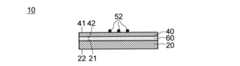
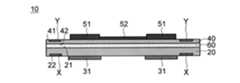
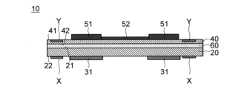
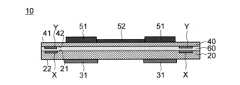
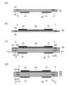
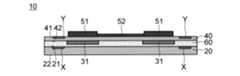
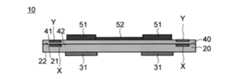
まず、本実施の形態に係る配線基板10について説明する。図1及び図2はそれぞれ、配線基板10を示す断面図及び平面図である。図1に示す断面図は、図2の配線基板10を線A-Aに沿って切断した場合の図である。
(wiring board)
First, thewiring substrate 10 according to this embodiment will be described. 1 and 2 are a cross-sectional view and a plan view, respectively, showing thewiring substrate 10. FIG. The cross-sectional view shown in FIG. 1 is a view when thewiring substrate 10 in FIG. 2 is cut along the line AA.

図1に示す配線基板10は、基材20、アライメントマーク部材X、電子部品用補強部材31、支持基板40、追加アライメントマーク部材Y、電子部品51、配線52を備える。以下、配線基板10の各構成要素について説明する。 Thewiring board 10 shown in FIG. 1 includes asubstrate 20 , an alignment mark member X, an electroniccomponent reinforcing member 31 , asupport substrate 40 , an additional alignment mark member Y, anelectronic component 51 andwiring 52 . Each component of thewiring board 10 will be described below.

〔基材〕
基材20は、伸縮性を有するよう構成された部材である。基材20は、電子部品51及び配線52側に位置する第1面21と、第1面21の反対側に位置する第2面22と、を含む。基材20の厚みは、例えば10mm以下であり、より好ましくは1mm以下である。基材20の厚みを小さくすることにより、基材20の伸縮に要する力を低減することができる。また、基材20の厚みを小さくすることにより、配線基板10を用いた製品全体の厚みを小さくすることができる。これにより、例えば、配線基板10を用いた製品が、人の腕などの身体の一部に取り付けるセンサである場合に、装着感を低減することができる。基材20の厚みは、10μm以上であってもよい。
〔Base material〕
Thebase material 20 is a member configured to have elasticity. Thebase material 20 includes afirst surface 21 located on theelectronic component 51 andwiring 52 side, and asecond surface 22 located on the opposite side of thefirst surface 21 . The thickness of thebase material 20 is, for example, 10 mm or less, and more preferably 1 mm or less. By reducing the thickness of thebase material 20, the force required for the expansion and contraction of thebase material 20 can be reduced. Moreover, by reducing the thickness of thebase material 20, the thickness of the entire product using thewiring board 10 can be reduced. As a result, for example, when the product using thewiring board 10 is a sensor attached to a part of the body such as an arm of a person, it is possible to reduce the wearing feeling. The thickness of thebase material 20 may be 10 μm or more.

基材20の伸縮性を表すパラメータの例として、基材20の弾性係数を挙げることができる。基材20の弾性係数は、例えば10MPa以下であり、より好ましくは1MPa以下である。このような弾性係数を有する基材20を用いることにより、配線基板10全体に伸縮性を持たせることができる。以下の説明において、基材20の弾性係数のことを、第1の弾性係数とも称する。基材20の第1の弾性係数は、1kPa以上であってもよい。 An example of a parameter representing the stretchability of thebase material 20 is the elastic modulus of thebase material 20 . The elastic modulus of thebase material 20 is, for example, 10 MPa or less, more preferably 1 MPa or less. By using thebase material 20 having such an elastic modulus, thewiring board 10 as a whole can be made stretchable. In the following description, the elastic modulus of thebase material 20 is also referred to as the first elastic modulus. The first elastic modulus of thebase material 20 may be 1 kPa or more.

基材20の第1の弾性係数を算出する方法としては、基材20のサンプルを用いて、JIS K6251に準拠して引張試験を実施するという方法を採用することができる。また、基材20のサンプルの弾性係数を、ISO14577に準拠してナノインデンテーション法によって測定するという方法を採用することもできる。ナノインデンテーション法において用いる測定器としては、ナノインデンターを用いることができる。基材20のサンプルを準備する方法としては、配線基板10から基材20の一部をサンプルとして取り出す方法や、配線基板10を構成する前の基材20の一部をサンプルとして取り出す方法が考えられる。その他にも、基材20の第1の弾性係数を算出する方法として、基材20を構成する材料を分析し、材料の既存のデータベースに基づいて基材20の第1の弾性係数を算出するという方法を採用することもできる。なお、本願における弾性係数は、25℃の環境下における弾性係数である。 As a method of calculating the first elastic modulus of thebase material 20, a method of performing a tensile test in accordance with JIS K6251 using a sample of thebase material 20 can be adopted. A method of measuring the elastic modulus of a sample of thebase material 20 by a nanoindentation method in compliance with ISO14577 can also be adopted. A nanoindenter can be used as a measuring instrument used in the nanoindentation method. As a method of preparing a sample of thebase material 20, a method of taking out a part of thebase material 20 from thewiring board 10 as a sample and a method of taking out a part of thebase material 20 before forming thewiring board 10 as a sample are considered. be done. In addition, as a method of calculating the first elastic modulus of thebase material 20, the material constituting thebase material 20 is analyzed, and the first elastic modulus of thebase material 20 is calculated based on an existing material database. method can also be adopted. In addition, the elastic modulus in this application is an elastic modulus in a 25 degreeC environment.

基材20の伸縮性を表すパラメータのその他の例として、基材20の曲げ剛性を挙げることができる。曲げ剛性は、対象となる部材の断面二次モーメントと、対象となる部材を構成する材料の弾性係数との積であり、単位はN・m又はPa・mである。基材20の断面二次モーメントは、配線基板10の伸縮方向に直交する平面によって、基材20のうち配線52と重なっている部分を切断した場合の断面に基づいて算出される。以下の説明において、基材20の曲げ剛性のことを、第1の曲げ剛性とも称する。Another example of the parameter representing the stretchability of thebase material 20 is the flexural rigidity of thebase material 20 . The bending stiffness is the product of the area moment of inertia of the target member and the elastic modulus of the material constituting the target member, and the unit is N·m2 or Pa·m4 . The geometrical moment of inertia of thebase material 20 is calculated based on a cross section obtained by cutting a portion of thebase material 20 that overlaps thewiring 52 with a plane perpendicular to the expansion/contraction direction of thewiring board 10 . In the following description, the flexural rigidity of thebase material 20 is also referred to as the first flexural rigidity.

基材20を構成する材料の例としては、熱可塑性エラストマー、シリコーンゴム、ウレタンゲル、シリコンゲル等を挙げることができる。また、基材20の材料として、例えば、織物、編物、不織布などの布を用いることもできる。熱可塑性エラストマーとしては、ポリウレタン系エラストマー、スチレン系熱可塑性エラストマー、オレフィン系熱可塑性エラストマー、塩ビ系熱可塑性エラストマー、エステル系熱可塑性エラストマー、アミド系熱可塑性エラストマー、1,2-BR系熱可塑性エラストマー、フッ素系熱可塑性エラストマー等を用いることができる。機械的強度や耐磨耗性を考慮すると、ウレタン系エラストマーを用いることが好ましい。さらに、シリコーンゴムは、耐熱性・耐薬品性・難燃性に優れており、基材20の材料として好ましい。なお、基材20には、埋設されたアライメントマーク部材Xが外部から視認できる必要がある場合は、例えば、透過性を有する材料が選択される。 Examples of materials forming thebase material 20 include thermoplastic elastomers, silicone rubbers, urethane gels, and silicone gels. As the material of thebase material 20, for example, cloth such as woven fabric, knitted fabric, and non-woven fabric can also be used. Thermoplastic elastomers include polyurethane-based elastomers, styrene-based thermoplastic elastomers, olefin-based thermoplastic elastomers, vinyl chloride-based thermoplastic elastomers, ester-based thermoplastic elastomers, amide-based thermoplastic elastomers, 1,2-BR-based thermoplastic elastomers, A fluorine-based thermoplastic elastomer or the like can be used. Considering mechanical strength and abrasion resistance, it is preferable to use a urethane-based elastomer. Furthermore, silicone rubber is excellent in heat resistance, chemical resistance, and flame resistance, and is preferable as a material for thebase material 20 . If the embedded alignment mark member X needs to be visible from the outside, for example, a transparent material is selected for thebase material 20 .

〔電子部品用補強部材〕
本実施の形態では、一例として、基材20の伸縮を制御するために電子部品用補強部材31を配線基板10に設けた例について説明する。しかしながら、配線基板10には、本実施の形態で適用されている電子部品用補強部材31に代えて、基材20の伸縮を制御するための他の部材や構成が適用されるようにしてもよく、電子部品用補強部材が省略されていてもよい。
この電子部品用補強部材31は、上述のように、基材20の伸縮を制御するために配線基板10に設けられた部材である。図1に示す例において、電子部品用補強部材31は、基材20の第2面22側に位置する。例えば、電子部品用補強部材31は、基材20の第2面22に設けられている。
[Reinforcing material for electronic parts]
In the present embodiment, as an example, an example in which thewiring board 10 is provided with the electroniccomponent reinforcing member 31 for controlling the expansion and contraction of thebase material 20 will be described. However, instead of the electroniccomponent reinforcing member 31 applied in the present embodiment, thewiring board 10 may be applied with other members or configurations for controlling the expansion and contraction of thebase material 20. Alternatively, the electronic component reinforcing member may be omitted.
The electroniccomponent reinforcing member 31 is a member provided on thewiring substrate 10 to control the expansion and contraction of thebase material 20 as described above. In the example shown in FIG. 1 , the electroniccomponent reinforcing member 31 is positioned on thesecond surface 22 side of thebase material 20 . For example, the electroniccomponent reinforcing member 31 is provided on thesecond surface 22 of thebase material 20 .

電子部品用補強部材31は、基材20の第1の弾性係数よりも大きい弾性係数を有する。電子部品用補強部材31の弾性係数は、例えば1GPa以上であり、より好ましくは10GPa以上である。電子部品用補強部材31の弾性係数は、基材20の第1の弾性係数の100倍以上であってもよく、1000倍以上であってもよい。このような電子部品用補強部材31を基材20に設けることにより、基材20のうち電子部品用補強部材31と重なる部分が伸縮することを抑制することができる。これにより、基材20を、伸縮が生じやすい部分と、伸縮が生じにくい部分とに区画することができる。以下の説明において、電子部品用補強部材31の弾性係数のことを、第2の弾性係数とも称する。電子部品用補強部材31の第2の弾性係数は、500GPa以下であってもよい。また、電子部品用補強部材31の第2の弾性係数は、基材20の第1の弾性係数の500000倍以下であってもよい。なお、「重なる」とは、基材20の第1面21の法線方向に沿って見た場合に2つの構成要素が重なることを意味している。 The electroniccomponent reinforcing member 31 has an elastic modulus larger than the first elastic modulus of thebase material 20 . The elastic modulus of the electroniccomponent reinforcing member 31 is, for example, 1 GPa or more, and more preferably 10 GPa or more. The elastic modulus of the electroniccomponent reinforcing member 31 may be 100 times or more, or 1000 times or more, the first elastic modulus of thebase material 20 . By providing such an electroniccomponent reinforcing member 31 on thebase material 20 , expansion and contraction of the portion of thebase material 20 that overlaps with the electroniccomponent reinforcing member 31 can be suppressed. As a result, thebase material 20 can be divided into a portion that easily expands and contracts and a portion that does not easily expand and contract. In the following description, the elastic modulus of the electroniccomponent reinforcing member 31 is also referred to as the second elastic modulus. The second elastic modulus of the electroniccomponent reinforcing member 31 may be 500 GPa or less. Further, the second elastic modulus of the electroniccomponent reinforcing member 31 may be 500000 times or less the first elastic modulus of thesubstrate 20 . Note that “overlapping” means that two components overlap when viewed along the normal direction of thefirst surface 21 of thebase material 20 .

電子部品用補強部材31の第2の弾性係数を算出する方法は、電子部品用補強部材31の形態に応じて適宜定められる。例えば、電子部品用補強部材31の第2の弾性係数を算出する方法は、上述の基材20の弾性係数を算出する方法と同様であってもよく、異なっていてもよい。後述する支持基板40の弾性係数も同様である。例えば、電子部品用補強部材31又は支持基板40の弾性係数を算出する方法として、電子部品用補強部材31又は支持基板40のサンプルを用いて、ASTM D882に準拠して引張試験を実施するという方法を採用することができる。 A method for calculating the second elastic modulus of the electroniccomponent reinforcing member 31 is appropriately determined according to the form of the electroniccomponent reinforcing member 31 . For example, the method for calculating the second elastic modulus of the electroniccomponent reinforcing member 31 may be the same as or different from the method for calculating the elastic modulus of thesubstrate 20 described above. The same applies to the elastic modulus of thesupport substrate 40, which will be described later. For example, as a method of calculating the elastic modulus of the electroniccomponent reinforcing member 31 or the supportingsubstrate 40, a sample of the electroniccomponent reinforcing member 31 or the supportingsubstrate 40 is used to perform a tensile test according to ASTM D882. can be adopted.

また、電子部品用補強部材31は、基材20の第1の曲げ剛性よりも大きい曲げ剛性を有する。電子部品用補強部材31の曲げ剛性は、基材20の第1の曲げ剛性の100倍以上であってもよく、1000倍以上であってもよい。以下の説明において、電子部品用補強部材31の曲げ剛性のことを、第2の曲げ剛性とも称する。 Further, the electroniccomponent reinforcing member 31 has bending rigidity greater than the first bending rigidity of thebase material 20 . The bending rigidity of the electroniccomponent reinforcing member 31 may be 100 times or more, or may be 1000 times or more, the first bending rigidity of thebase material 20 . In the following description, the flexural rigidity of the electroniccomponent reinforcing member 31 is also referred to as the second flexural rigidity.

電子部品用補強部材31を構成する材料の例としては、金属材料を含む金属層や、一般的な熱可塑性エラストマー、アクリル系、ウレタン系、エポキシ系、ポリエステル系、エポキシ系、ビニルエーテル系、ポリエン・チオール系、シリコーン系等のオリゴマー、ポリマー等を挙げることができる。金属材料の例としては、銅、アルミニウム、ステンレス鋼等を挙げることができる。電子部品用補強部材31の厚みは、例えば10μm以上である。上述の材料のうち、金属層は、弾性率が大きくエッチング加工などにより微細加工可能であり、より好ましい。
また、電子部品用補強部材31の材料例として、PETフィルム、PENフィルム等も適用可能であり、例えば、ポリエチレンナフタレート、ポリイミド、ポリカーボネート、アクリル樹脂、ポリエチレンテレフタラート等を用いることができる。
Examples of materials constituting the electroniccomponent reinforcing member 31 include metal layers containing metal materials, general thermoplastic elastomers, acrylics, urethanes, epoxies, polyesters, epoxies, vinyl ethers, polyenes, Thiol-based, silicone-based oligomers, polymers, and the like can be mentioned. Examples of metal materials include copper, aluminum, stainless steel, and the like. The thickness of the electroniccomponent reinforcing member 31 is, for example, 10 μm or more. Among the above materials, the metal layer is more preferable because it has a large elastic modulus and can be finely processed by etching or the like.
PET film, PEN film, etc., can also be applied as material examples of the electroniccomponent reinforcing member 31, and for example, polyethylene naphthalate, polyimide, polycarbonate, acrylic resin, polyethylene terephthalate, etc. can be used.

電子部品用補強部材31を構成する材料として、オリゴマー又はポリマーを用いる場合、電子部品用補強部材31は、透明性を有していてもよい。また、電子部品用補強部材31は、遮光性、例えば紫外線を遮蔽する特性を有していてもよい。例えば、電子部品用補強部材31は黒色であってもよい。また、電子部品用補強部材31の色と基材20の色とが同一であってもよい。 When an oligomer or polymer is used as the material forming the electroniccomponent reinforcing member 31, the electroniccomponent reinforcing member 31 may have transparency. Further, the electroniccomponent reinforcing member 31 may have a light shielding property, for example, a property of shielding ultraviolet rays. For example, the electroniccomponent reinforcing member 31 may be black. Further, the color of the electroniccomponent reinforcing member 31 and the color of thebase material 20 may be the same.

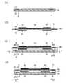
図3は、図2の配線基板10を線B-Bに沿って切断した場合を示す断面図である。なお、図2は、配線基板10を基材20の第1面21側から見た場合を示す平面図であるので、基材20の第1面21側に位置するアライメントマーク部材X及び第2面22側に位置する電子部品用補強部材31は点線で表されている。 FIG. 3 is a cross-sectional view showing thewiring board 10 of FIG. 2 cut along the line BB. 2 is a plan view showing thewiring board 10 viewed from the side of thefirst surface 21 of thesubstrate 20, the alignment mark member X and the second alignment mark member X located on the side of thefirst surface 21 of thesubstrate 20 are shown in FIG. The electroniccomponent reinforcing member 31 located on the side of thesurface 22 is indicated by a dotted line.

〔支持基板〕
支持基板40は、基材20よりも低い伸縮性を有するよう構成された板状の部材である。支持基板40は、基材20側に位置する第2面42と、第2面42の反対側に位置する第1面41と、を含む。図1に示す例において、支持基板40は、その第1面41側において電子部品51及び配線52を支持している。また、支持基板40は、その第2面42側において基材20の第1面に接合されている。例えば、基材20と支持基板40との間に、接着剤を含む接着層60が設けられていてもよい。接着層60を構成する材料としては、例えばアクリル系接着剤、シリコーン系接着剤等を用いることができる。接着層60の厚みは、例えば5μm以上且つ200μm以下である。また、図22に示すように、常温接合又は分子接着によって支持基板40の第2面42が基材20の第1面21に接合されていてもよい。この場合、基材20と支持基板40との間に接着層が設けられていなくてもよい。また、基材20の第1面21又は支持基板40の第2面42の一方又は両方に、常温接合、分子接着の接着性を向上させるプライマー層を設けてもよい。常温接合又は分子接着によって支持基板40の第2面42が基材20の第1面21に接合される場合、図23に示すように、電子部品用補強部材31は、基材20の第1面21又は第2面22に露出しないよう基材20に埋め込まれていることが好ましい。
[Supporting substrate]
Thesupport substrate 40 is a plate-like member configured to have lower stretchability than thebase material 20 . Thesupport substrate 40 includes asecond surface 42 located on thesubstrate 20 side and afirst surface 41 located on the opposite side of thesecond surface 42 . In the example shown in FIG. 1, thesupport substrate 40 supports theelectronic component 51 and thewiring 52 on thefirst surface 41 side. Also, thesupport substrate 40 is bonded to the first surface of thebase material 20 on thesecond surface 42 side thereof. For example, anadhesive layer 60 containing an adhesive may be provided between thebase material 20 and thesupport substrate 40 . As a material forming theadhesive layer 60, for example, an acrylic adhesive, a silicone adhesive, or the like can be used. The thickness of theadhesive layer 60 is, for example, 5 μm or more and 200 μm or less. Alternatively, as shown in FIG. 22, thesecond surface 42 of thesupport substrate 40 may be bonded to thefirst surface 21 of thebase material 20 by room temperature bonding or molecular bonding. In this case, an adhesive layer may not be provided between thebase material 20 and thesupport substrate 40 . In addition, a primer layer that improves room-temperature bonding and molecular adhesion may be provided on one or both of thefirst surface 21 of thebase material 20 and thesecond surface 42 of thesupport substrate 40 . When thesecond surface 42 of thesupport substrate 40 is bonded to thefirst surface 21 of thebase material 20 by room temperature bonding or molecular bonding, as shown in FIG. It is preferably embedded in thesubstrate 20 so as not to be exposed on thesurface 21 or thesecond surface 22 .

後述するように、支持基板40に接合された基材20から引張応力が取り除かれて基材20が収縮するとき、支持基板40には蛇腹形状部が形成される。支持基板40の特性や寸法は、このような蛇腹形状部が形成され易くなるよう設定されている。例えば、支持基板40は、基材20の第1の弾性係数よりも大きい弾性係数を有する。以下の説明において、支持基板40の弾性係数のことを、第3の弾性係数とも称する。 As will be described later, when the tensile stress is removed from thesubstrate 20 bonded to thesupport substrate 40 and thesubstrate 20 contracts, thesupport substrate 40 forms a bellows-shaped portion. The characteristics and dimensions of thesupport substrate 40 are set so as to facilitate the formation of such a bellows-shaped portion. For example, thesupport substrate 40 has an elastic modulus greater than the first elastic modulus of thesubstrate 20 . In the following description, the elastic modulus of thesupport substrate 40 is also referred to as the third elastic modulus.

支持基板40の第3の弾性係数は、例えば100MPa以上であり、より好ましくは1GPa以上である。支持基板40の第3の弾性係数は、基材20の第1の弾性係数の100倍以上であってもよく、1000倍以上であってもよい。また、支持基板40の厚みは、例えば10μm以下であり、より好ましくは5μm以下である。支持基板40の弾性係数を高くしたり、支持基板40の厚みを小さくしたりすることにより、基材20の収縮に伴って支持基板40に蛇腹形状部が形成され易くなる。支持基板40を構成する材料としては、例えば、ポリエチレンナフタレート、ポリイミド、ポリカーボネート、アクリル樹脂、ポリエチレンテレフタラート等を用いることができる。なお、支持基板40には、埋設された追加アライメントマーク部材Yが外部から視認できる必要がある場合は、例えば、透過性を有する材料が選択される。 The third elastic modulus of thesupport substrate 40 is, for example, 100 MPa or more, more preferably 1 GPa or more. The third elastic modulus of thesupport substrate 40 may be 100 times or more, or 1000 times or more, the first elastic modulus of thebase material 20 . Also, the thickness of thesupport substrate 40 is, for example, 10 μm or less, and more preferably 5 μm or less. By increasing the elastic modulus of the supportingsubstrate 40 or decreasing the thickness of the supportingsubstrate 40, the bellows-shaped portion is easily formed in the supportingsubstrate 40 as thebase material 20 shrinks. Examples of materials that can be used for thesupport substrate 40 include polyethylene naphthalate, polyimide, polycarbonate, acrylic resin, and polyethylene terephthalate. If the additional alignment mark member Y embedded in thesupport substrate 40 needs to be visible from the outside, for example, a transparent material is selected.

支持基板40の第3の弾性係数は、基材20の第1の弾性係数の100倍以下であってもよい。支持基板40の第3の弾性係数を算出する方法は、基材20の場合と同様である。また、支持基板40の厚みは、500nm以上であってもよい。 The third modulus of elasticity of thesupport substrate 40 may be 100 times or less the first modulus of elasticity of thesubstrate 20 . The method for calculating the third elastic modulus of thesupport substrate 40 is the same as for thebase material 20 . Moreover, the thickness of thesupport substrate 40 may be 500 nm or more.

〔電子部品〕
図1に示す例において、電子部品51は、配線52に接続される電極を少なくとも有する。電子部品51は、能動部品であってもよく、受動部品であってもよく、機構部品であってもよい。
電子部品51の例としては、トランジスタ、LSI(Large-Scale Integration)、MEMS(Micro Electro Mechanical Systems)、リレー、LED、OLED、LCDなどの発光素子、センサ、ブザー等の発音部品、振動を発する振動部品、冷却発熱をコントロールするペルチェ素子や電熱線などの冷発熱部品、抵抗器、キャパシタ、インダクタ、圧電素子、スイッチ、コネクタなどを挙げることができる。電子部品51の上述の例のうち、センサが好ましく用いられる。センサとしては、例えば、温度センサ、圧力センサ、光センサ、光電センサ、近接センサ、せん断力センサ、生体センサ、レーザーセンサ、マイクロ波センサ、湿度センサ、歪みセンサ、ジャイロセンサ、加速度センサ、変位センサ、磁気センサ、ガスセンサ、GPSセンサ、超音波センサ、臭いセンサ、脳波センサ、電流センサ、振動センサ、脈波センサ、心電センサ、光度センサ等を挙げることができる。これらのセンサのうち、生体センサが特に好ましい。生体センサは、心拍や脈拍、心電、血圧、体温、血中酸素濃度等の生体情報を測定することができる。
[Electronic parts]
In the example shown in FIG. 1 ,electronic component 51 has at least electrodes connected towiring 52 . Theelectronic component 51 may be an active component, a passive component, or a mechanical component.
Examples of theelectronic components 51 include transistors, LSIs (Large-Scale Integration), MEMS (Micro Electro Mechanical Systems), relays, light-emitting elements such as LEDs, OLEDs, and LCDs, sound components such as sensors and buzzers, and vibrations that generate vibrations. Components, cooling/heating components such as Peltier elements and heating wires for controlling cooling heat generation, resistors, capacitors, inductors, piezoelectric elements, switches, connectors, and the like can be mentioned. Of the above examples ofelectronic components 51, sensors are preferably used. Examples of sensors include temperature sensors, pressure sensors, optical sensors, photoelectric sensors, proximity sensors, shear force sensors, biological sensors, laser sensors, microwave sensors, humidity sensors, strain sensors, gyro sensors, acceleration sensors, displacement sensors, A magnetic sensor, a gas sensor, a GPS sensor, an ultrasonic sensor, an odor sensor, an electroencephalogram sensor, a current sensor, a vibration sensor, a pulse wave sensor, an electrocardiogram sensor, a light intensity sensor, and the like can be mentioned. Of these sensors, biosensors are particularly preferred. A biological sensor can measure biological information such as heartbeat, pulse, electrocardiogram, blood pressure, body temperature, and blood oxygen concentration.

〔配線〕
配線52は、電子部品51の電極に接続された、導電性を有する部材である。例えば図2に示すように、配線52の一端及び他端が、2つの電子部品51の電極にそれぞれ接続されている。図2に示すように、複数の配線52が2つの電子部品51の間に設けられていてもよい。
〔wiring〕
Thewiring 52 is a conductive member connected to the electrodes of theelectronic component 51 . For example, as shown in FIG. 2, one end and the other end ofwiring 52 are connected to electrodes of twoelectronic components 51, respectively. As shown in FIG. 2,multiple wirings 52 may be provided between twoelectronic components 51 .

後述するように、支持基板40に接合された基材20から引張応力が取り除かれて基材20が収縮するとき、配線52は蛇腹状に変形する。この点を考慮し、好ましくは、配線52は、変形に対する耐性を有する構造を備える。例えば、配線52は、ベース材と、ベース材の中に分散された複数の導電性粒子とを有する。この場合、ベース材として、樹脂などの変形可能な材料を用いることにより、基材20の伸縮に応じて配線52も変形することができる。また、変形が生じた場合であっても複数の導電性粒子の間の接触が維持されるように導電性粒子の分布や形状を設定することにより、配線52の導電性を維持することができる。 As will be described later, when the tensile stress is removed from thebase material 20 joined to thesupport substrate 40 and thebase material 20 contracts, thewiring 52 deforms into a bellows shape. With this in mind, thewiring 52 preferably has a structure that is resistant to deformation. For example,line 52 has a base material and a plurality of conductive particles dispersed within the base material. In this case, by using a deformable material such as resin as the base material, thewiring 52 can also be deformed according to the expansion and contraction of thebase material 20 . In addition, the conductivity of thewiring 52 can be maintained by setting the distribution and shape of the conductive particles so that the contact between the plurality of conductive particles is maintained even when deformation occurs. .

配線52のベース材を構成する材料としては、例えば、一般的な熱可塑性エラストマーおよび熱硬化性エラストマーを用いることができ、例えば、スチレン系エラストマー、アクリル系エラストマー、オレフィン系エラストマー、ウレタン系エラストマー、シリコーンゴム、ウレタンゴム、フッ素ゴム、ニトリルゴム、ポリブタジエン、ポリクロロプレン等を用いることができる。中でも、ウレタン系、シリコーン系構造を含む樹脂やゴムが、その伸縮性や耐久性などの面から好ましく用いられる。また、配線52の導電性粒子を構成する材料としては、例えば銀、銅、金、ニッケル、パラジウム、白金、カーボン等の粒子を用いることができる。中でも、銀粒子が、価格と導電性の観点から好ましく用いられる。 As a material constituting the base material of thewiring 52, for example, general thermoplastic elastomers and thermosetting elastomers can be used. Rubber, urethane rubber, fluororubber, nitrile rubber, polybutadiene, polychloroprene, and the like can be used. Among them, resins and rubbers containing urethane-based or silicone-based structures are preferably used in terms of stretchability and durability. Also, as a material forming the conductive particles of thewiring 52, particles such as silver, copper, gold, nickel, palladium, platinum, and carbon can be used. Among them, silver particles are preferably used from the viewpoint of price and conductivity.

なお、配線52に求められることは、蛇腹形状部57の解消及び生成を利用して基材20の伸張及び収縮に追従することである。この点を考慮すると、配線52の材料としては、上述のようにそれ自体が変形性や伸縮性を有しているものだけでなく、それ自体は変形性や伸縮性を有していないものも採用可能である。
配線52に用いられ得る、それ自体は伸縮性を有さない材料としては、例えば、金、銀、銅、アルミニウム、白金、クロム等の金属や、これらの金属を含む合金が挙げられる。配線52の材料自体が伸縮性を有さない場合、配線52としては、金属膜を用いることができる。
Note that thewiring 52 is required to follow the expansion and contraction of thebase material 20 by utilizing the elimination and generation of the bellows-shapedportion 57 . Considering this point, the material of thewiring 52 is not limited to the material that itself has deformability and stretchability as described above, but also the material that itself does not have deformability and stretchability. Adoptable.
Examples of materials that can be used for thewiring 52 and that do not have elasticity per se include metals such as gold, silver, copper, aluminum, platinum, and chromium, and alloys containing these metals. A metal film can be used as thewiring 52 when the material of thewiring 52 itself does not have elasticity.

配線52の厚みは、電子部品51の厚みよりも小さく、例えば50μm以下である。配線52の幅は、例えば50μm以上且つ10mm以下である。 The thickness of thewiring 52 is smaller than the thickness of theelectronic component 51, for example, 50 μm or less. The width of thewiring 52 is, for example, 50 μm or more and 10 mm or less.

〔電子部品用補強部材の位置関係〕
次に、電子部品用補強部材31について、電子部品51及び配線52との位置関係に基づいて説明する。
[Positional relationship of reinforcing members for electronic components]
Next, the electroniccomponent reinforcing member 31 will be described based on the positional relationship between theelectronic component 51 and thewiring 52 .

図1及び図2に示すように、電子部品用補強部材31は、基材20の第1面21の法線方向に沿って見た場合に電子部品51と少なくとも部分的に重なるように配置されている。好ましくは、電子部品用補強部材31は、基材20の第1面21の法線方向に沿って見た場合に電子部品51の全域にわたって電子部品51に重なっている。このため、基材20のうち電子部品51と重なる部分は、すなわち電子部品用補強部材31と重なる部分は、基材20のうち電子部品用補強部材31と重ならない部分に比べて変形しにくい。これにより、基材20に引張応力などの力を加えたときや、基材20から引張応力などの力を取り除いたときなどに、基材20のうち電子部品51と重なる部分に変形が生じることを抑制することができる。このことにより、基材20の変形に起因する応力が電子部品51に加わることを抑制することができ、電子部品51が変形したり破損したりしてしまうことを抑制することができる。また、電子部品51と配線52との間の電気接合部が破損してしまうことを抑制することができる。 As shown in FIGS. 1 and 2 , the electroniccomponent reinforcing member 31 is arranged so as to at least partially overlap theelectronic component 51 when viewed along the normal direction of thefirst surface 21 of thebase material 20 . ing. Preferably, the electroniccomponent reinforcing member 31 overlaps theelectronic component 51 over the entire area of theelectronic component 51 when viewed along the normal direction of thefirst surface 21 of thebase material 20 . Therefore, the portion of thesubstrate 20 that overlaps theelectronic component 51 , that is, the portion that overlaps the electroniccomponent reinforcing member 31 is less likely to deform than the portion of thesubstrate 20 that does not overlap the electroniccomponent reinforcing member 31 . Accordingly, when a force such as a tensile stress is applied to thebase material 20 or when a force such as a tensile stress is removed from thebase material 20, the portion of thebase material 20 that overlaps theelectronic component 51 is not deformed. can be suppressed. As a result, it is possible to suppress the application of stress to theelectronic component 51 caused by the deformation of thebase material 20 , thereby suppressing the deformation or breakage of theelectronic component 51 . Moreover, it is possible to prevent damage to the electrical joint between theelectronic component 51 and thewiring 52 .

なお、図1においては、基材20の第2面22に電子部品用補強部材31が位置する例が示されているが、電子部品用補強部材31の位置は任意である。例えば、基材20の第1面21に電子部品用補強部材31が位置していてもよい。 Although FIG. 1 shows an example in which the electroniccomponent reinforcing member 31 is positioned on thesecond surface 22 of thebase material 20, the position of the electroniccomponent reinforcing member 31 is arbitrary. For example, the electroniccomponent reinforcing member 31 may be positioned on thefirst surface 21 of thebase material 20 .

〔アライメントマーク部材と追加アライメントマーク部材〕
アライメントマーク部材Xは、例えば、図1、図2に示すように、基材20に設けられている。図1の例では、アライメントマーク部材Xは、基材20の中に位置している。特に、図1の例では、アライメントマーク部材Xは、基材20の第1面21に露出するように、基材20の中の第1面21側に位置している。
[Alignment mark member and additional alignment mark member]
The alignment mark member X is provided on thesubstrate 20 as shown in FIGS. 1 and 2, for example. In the example of FIG. 1, the alignment mark member X is positioned inside thebase material 20 . In particular, in the example of FIG. 1, the alignment mark member X is located on thefirst surface 21 side of thesubstrate 20 so as to be exposed on thefirst surface 21 of thesubstrate 20 .

このアライメントマーク部材Xは、配線基板10の製造時の位置合わせ、及び/又は、図示しない被実装体に対する配線基板10の実装時の位置合わせに用いられるようになっている。なお、当該被実装体は、例えば、人体などの生体であるが、人体等の生体以外の物体であってもよい。 The alignment mark member X is used for alignment during manufacture of thewiring board 10 and/or alignment during mounting of thewiring board 10 on a mounted body (not shown). The mounted body is, for example, a living body such as a human body, but may be an object other than a living body such as a human body.

そして、基材20の伸張時及び収縮時において、アライメントマーク部材Xの形状及び大きさが変化しないようになっている。なお、このアライメントマーク部材Xの大きさは、例えば、基材20の伸張率に基づいて設定されている。 Further, the shape and size of the alignment mark member X are not changed when thebase material 20 is expanded and contracted. The size of the alignment mark member X is set based on the elongation rate of thebase material 20, for example.

なお、基材20の第1面21の法線方向に沿って見た場合にアライメントマーク部材Xが形成されている領域に少なくとも部分的に重なり、第1の弾性係数よりも大きい弾性係数を有するマーク用補強部材を、備えるようにしてもよい。また、このマーク用補強部材は、例えば、金属層を含むようにしてもよい。なお、図1、図2の例では、当該マーク用補強部材は、アライメントマーク部材Xと一体になっている。 In addition, when viewed along the normal direction of thefirst surface 21 of thebase material 20, it at least partially overlaps the region where the alignment mark member X is formed, and has an elastic modulus larger than the first elastic modulus. A marking reinforcing member may be provided. Also, the mark reinforcing member may include, for example, a metal layer. 1 and 2, the mark reinforcing member is integrated with the alignment mark member X. As shown in FIG.

そして、例えば、配線52のうち基材20の第1面21の法線方向に沿って見た場合に、当該マーク用補強部材、すなわち、アライメントマーク部材Xと重ならない部分は、基材20の第1面21の面内方向に沿って並ぶ複数の山部及び谷部を含む蛇腹形状部を有するようになっている。 Then, for example, when viewed along the normal direction of thefirst surface 21 of thebase material 20 in thewiring 52 , the portion that does not overlap the mark reinforcing member, that is, the alignment mark member X is the part of thebase material 20 . It has a bellows-shaped portion including a plurality of peaks and valleys arranged along the in-plane direction of thefirst surface 21 .

また、追加アライメントマーク部材Yは、図1、図2に示すように、支持基板40に設けられている。図1の例では、追加アライメントマーク部材Yは、支持基板40の中に位置している。特に、図1の例では、追加アライメントマーク部材Yは、支持基板40の第1面41に露出するように、支持基板40の中の第1面41側に位置している。 Further, the additional alignment mark member Y is provided on thesupport substrate 40 as shown in FIGS. In the example of FIG. 1, the additional alignment mark member Y is located within thesupport substrate 40 . In particular, in the example of FIG. 1, the additional alignment mark member Y is positioned on thefirst surface 41 side of thesupport substrate 40 so as to be exposed on thefirst surface 41 of thesupport substrate 40 .

この追加アライメントマーク部材Yは、基材20に支持基板40を貼り合わせるときに、基材20の第1面21の法線方向に沿って見た場合に、アライメントマーク部材と予め規定された所定の位置関係で重なるようにすることで、基材20と支持基板40とを所定の位置に位置合わせするための部材である。 When thesupport substrate 40 is bonded to thebase material 20, the additional alignment mark member Y is an alignment mark member and a predetermined value when viewed along the normal direction of thefirst surface 21 of thebase material 20. It is a member for aligning thebase material 20 and thesupport substrate 40 at a predetermined position by overlapping with the positional relationship of .

例えば、アライメントマーク部材Xと追加アライメントマーク部材Yとを合成した1つのアライメントマークとして、被実装体に対する配線基板10の実装時の位置合わせに用いられるようになっている。 For example, one alignment mark obtained by synthesizing the alignment mark member X and the additional alignment mark member Y is used for alignment when thewiring board 10 is mounted on the mounted body.

また、被実装体に対する配線基板10の実装時の位置合わせに用いる場合において、基材20の第1面21の法線方向に沿って見た場合に、被実装体、例えば、人体の予め規定された位置、例えば、血管位置とアライメントマーク部材Xの位置とが所定の位置関係になるように配線基板10を当該被実装体に実装した状態で、必要な情報、例えば、血圧等を被実装体から検出できるように、配線基板10におけるアライメントマーク部材Xの位置が設定されている。 In addition, when used for alignment during mounting of thewiring board 10 on a mounted body, when viewed along the normal direction of thefirst surface 21 of thebase material 20, the mounted body, for example, the human body, is defined in advance. Necessary information, such as blood pressure, etc. The position of the alignment mark member X on thewiring board 10 is set so that it can be detected from the body.

ここで、配線基板のアライメントマーク部材Xと追加アライメントマーク部材Yの配置は、図1に示す構成に限られない。図4ないし図13は、配線基板のアライメントマーク部材Xと追加アライメントマーク部材Yの配置の他の例を示す断面図である。 Here, the arrangement of the alignment mark member X and the additional alignment mark member Y on the wiring board is not limited to the configuration shown in FIG. 4 to 13 are cross-sectional views showing other examples of the arrangement of the alignment mark member X and the additional alignment mark member Y on the wiring board.

例えば、図4に示すように、アライメントマーク部材Xは、基材20の第2面22に露出するように、基材20の中の第2面22側に位置しているようにしてもよい。 For example, as shown in FIG. 4, the alignment mark member X may be positioned on thesecond surface 22 side of thesubstrate 20 so as to be exposed on thesecond surface 22 of thesubstrate 20. .

また、図5に示すように、アライメントマーク部材Xは、基材20の中に位置し、基材20の第1面21から第2面22に向かう方向において、アライメントマーク部材Xの厚さは、基材20の厚さよりも、小さくなるようにしてもよい。 Further, as shown in FIG. 5, the alignment mark member X is positioned in thebase material 20, and the thickness of the alignment mark member X in the direction from thefirst surface 21 to thesecond surface 22 of thebase material 20 is , may be smaller than the thickness of thesubstrate 20 .

また、図6に示すように、アライメントマーク部材Xは、基材20の第1面21と第2面22との間を貫通するように、基材20の中に位置しているようにしてもよい。特に、この場合、図6に示すように、基材20の第1面21から第2面22に向かう方向において、アライメントマーク部材Xの厚さは、基材20の厚さと同じであるようにしてもよい。 Further, as shown in FIG. 6, the alignment mark member X is positioned in thebase material 20 so as to penetrate between thefirst surface 21 and thesecond surface 22 of thebase material 20. good too. In particular, in this case, as shown in FIG. 6, the thickness of the alignment mark member X should be the same as the thickness of thesubstrate 20 in the direction from thefirst surface 21 to thesecond surface 22 of thesubstrate 20. may

また、図7に示すように、アライメントマーク部材Xは、基材20の第1面21上に位置しているようにしてもよい。 Also, as shown in FIG. 7, the alignment mark member X may be positioned on thefirst surface 21 of thebase material 20 .

また、図8に示すように、アライメントマーク部材Xは、基材20の第2面22上に位置しているようにしてもよい。 Also, as shown in FIG. 8, the alignment mark member X may be positioned on thesecond surface 22 of thebase material 20 .

一方、例えば、図4に示すように、追加アライメントマーク部材Yは、支持基板40の第1面41に露出するように、支持基板40の中の第1面41側に位置しているようにしてもよい。 On the other hand, for example, as shown in FIG. 4, the additional alignment mark member Y is positioned on thefirst surface 41 side of thesupport substrate 40 so as to be exposed on thefirst surface 41 of thesupport substrate 40. may

また、図9に示すように、追加アライメントマーク部材Yは、支持基板40の第2面42に露出するように、支持基板40の中の第2面42側に位置しているようにしてもよい。 Further, as shown in FIG. 9, the additional alignment mark member Y may be positioned on thesecond surface 42 side of thesupport substrate 40 so as to be exposed on thesecond surface 42 of thesupport substrate 40. good.

また、図10に示すように、追加アライメントマーク部材Yは、支持基板40の中に位置し、支持基板40の第1面41から第2面42に向かう方向において、追加アライメントマーク部材Yの厚さは、支持基板40の厚さよりも小さくなるようにしてもよい。 Further, as shown in FIG. 10, the additional alignment mark member Y is positioned in thesupport substrate 40, and the thickness of the additional alignment mark member Y in the direction from thefirst surface 41 to thesecond surface 42 of thesupport substrate 40 is The thickness may be smaller than the thickness of thesupport substrate 40 .

また、図11に示すように、追加アライメントマーク部材Yは、支持基板40の第1面41と第2面42との間を貫通するように、支持基板40の中に位置しているようにしてもよい。特に、この場合、図11に示すように、支持基板40の第1面41から第2面42に向かう方向において、追加アライメントマーク部材Yの厚さは、支持基板40の厚さと同じであるようにしてもよい。 Further, as shown in FIG. 11, the additional alignment mark member Y is positioned in thesupport substrate 40 so as to penetrate between thefirst surface 41 and thesecond surface 42 of thesupport substrate 40. may In particular, in this case, as shown in FIG. 11, the thickness of the additional alignment mark member Y should be the same as the thickness of thesupport substrate 40 in the direction from thefirst surface 41 to thesecond surface 42 of thesupport substrate 40. can be

また、図12に示すように、追加アライメントマーク部材Yは、支持基板40の第1面41上に位置しているようにしてもよい。 Further, as shown in FIG. 12, the additional alignment mark member Y may be positioned on thefirst surface 41 of thesupport substrate 40. As shown in FIG.

また、図13に示すように、追加アライメントマーク部材Yは、支持基板40の第2面42上に位置しているようにしてもよい。 Further, as shown in FIG. 13, the additional alignment mark member Y may be positioned on thesecond surface 42 of thesupport substrate 40. As shown in FIG.

なお、各図の例では、1つのアライメントマーク部材Xは1つのパターンで構成されているが、これに限られるものでは無く、アライメントマーク部材Xは、複数のパターンで構成されているようにしてもよい。 Although one alignment mark member X is composed of one pattern in the example of each figure, it is not limited to this, and the alignment mark member X may be composed of a plurality of patterns. good too.

なお、図2の例では、配線52のうち基材20の第1面21の法線方向に沿って見た場合に、アライメントマーク部材X及び追加アライメントマーク部材Yの形状が正方形である。しかしながら、配線52のうち基材20の第1面21の法線方向に沿って見た場合に、アライメントマーク部材X及び追加アライメントマーク部材Yは、例えば、多角形状、十字形状、又は、円形状を有するようにしてもよい。また、アライメントマーク部材Xとして読取可能な形状であれば数字や文字等を有するようにしてもよい。 In the example of FIG. 2, when viewed along the normal direction of thefirst surface 21 of thebase material 20 in thewiring 52, the shape of the alignment mark member X and the additional alignment mark member Y is square. However, when viewed along the normal direction of thefirst surface 21 of thesubstrate 20 in thewiring 52, the alignment mark member X and the additional alignment mark member Y are, for example, polygonal, cross-shaped, or circular. may have Also, the alignment mark member X may have numbers, letters, or the like as long as it has a readable shape.

〔配線の構造〕
続いて、配線52の断面構造について、図14を参照して詳細に説明する。図14は、図1に示す配線基板1010の配線52及びその周辺の構成要素の一例を拡大して示す断面図である。
[Wiring structure]
Next, the cross-sectional structure of thewiring 52 will be described in detail with reference to FIG. FIG. 14 is a cross-sectional view showing an enlarged example of thewiring 52 of the wiring board 1010 shown in FIG. 1 and its surrounding components.

図1乃至図3に示すように、配線52全体は、若しくは配線52の大部分は、電子部品用補強部材31と重ならないように配置されている。このため、基材20に収縮などの変形が生じたとき、配線52は、基材20の変形に伴って変形し易い。例えば、伸長させた状態の基材20に配線52を設けた後、基材20を弛緩させると、図14に示すように、配線52のうち電子部品用補強部材31と重なっていない部分に、蛇腹形状部57が生じる。 As shown in FIGS. 1 to 3 , theentire wiring 52 or most of thewiring 52 is arranged so as not to overlap the electroniccomponent reinforcing member 31 . Therefore, when deformation such as shrinkage occurs in thebase material 20 , thewiring 52 is likely to be deformed along with the deformation of thebase material 20 . For example, when thewiring 52 is provided on the stretchedbase material 20 and then thebase material 20 is relaxed, as shown in FIG. A bellows-shapedportion 57 is produced.

蛇腹形状部57は、基材20の第1面21の法線方向における山部及び谷部を含む。図14において、符号53は、配線52の表面に現れる山部を表し、符号54は、配線52の裏面に現れる山部を表す。また、符号55は、配線52の表面に現れる谷部を表し、符号56は、配線52の裏面に現れる谷部を表す。表面とは、配線52の面のうち基材20から遠い側に位置する面であり、裏面とは、配線52の面のうち基材20に近い側に位置する面である。また、図14において、符号26及び27は、基材20の第1面21に現れる山部及び谷部を表す。第1面21に山部26及び谷部27が現れるように基材20が変形することにより、配線52が蛇腹状に変形して蛇腹形状部57を有するようになる。基材20の第1面21の山部26が、配線52の蛇腹形状部57の山部53,54に対応し、基材20の第1面21の谷部27が、配線52の蛇腹形状部57の谷部55,56に対応している。 The bellows-shapedportion 57 includes peaks and valleys in the normal direction of thefirst surface 21 of thebase material 20 . In FIG. 14,reference numeral 53 denotes a ridge appearing on the front surface of thewiring 52, andreference numeral 54 denotes a ridge appearing on the back surface of thewiring 52. In FIG.Reference numeral 55 denotes valleys appearing on the front surface of thewiring 52, andreference numeral 56 denotes valleys appearing on the back surface of thewiring 52. FIG. The front surface is the surface of thewiring 52 that is farther from thesubstrate 20 , and the back surface is the surface of thewiring 52 that is closer to thesubstrate 20 . 14,reference numerals 26 and 27 represent peaks and valleys appearing on thefirst surface 21 of thesubstrate 20. As shown in FIG. By deforming thebase material 20 so that thepeaks 26 and thevalleys 27 appear on thefirst surface 21 , thewiring 52 is deformed into a bellows shape and has a bellows-shapedportion 57 . Thepeaks 26 of thefirst surface 21 of thesubstrate 20 correspond to thepeaks 53 and 54 of the accordion-shapedportion 57 of thewiring 52, and thevalleys 27 of thefirst surface 21 of thesubstrate 20 correspond to the accordion-shape of thewiring 52. Corresponds to thetroughs 55 and 56 of theportion 57 .

山部53,54及び谷部55,56は、基材20の第1面21の面内方向に沿って繰り返し現れる。山部53,54及び谷部55,56が繰り返し現れる周期Fは、例えば10μm以上且つ100mm以下である。なお、図14においては、蛇腹形状部57の複数の山部及び谷部が一定の周期で並ぶ例が示されているが、これに限られることはない。図示はしないが、蛇腹形状部57の複数の山部及び谷部は、第1面21の面内方向に沿って不規則に並んでいてもよい。例えば、第1面21の面内方向において隣り合う2つの山部の間の間隔が一定でなくてもよい。 Thepeaks 53 and 54 and thevalleys 55 and 56 appear repeatedly along the in-plane direction of thefirst surface 21 of thesubstrate 20 . A period F at which thepeaks 53 and 54 and thevalleys 55 and 56 appear repeatedly is, for example, 10 μm or more and 100 mm or less. Although FIG. 14 shows an example in which a plurality of ridges and troughs of the bellows-shapedportion 57 are arranged at regular intervals, the present invention is not limited to this. Although not shown, the plurality of peaks and valleys of the bellows-shapedportion 57 may be arranged irregularly along the in-plane direction of thefirst surface 21 . For example, the interval between two peaks adjacent to each other in the in-plane direction of thefirst surface 21 may not be constant.

図14において、符号S1は、配線52の表面における蛇腹形状部57の振幅を表す。振幅S1は、例えば1μm以上であり、より好ましくは10μm以上である。振幅S1を10μm以上とすることにより、基材20の伸張に追従して配線52が変形し易くなる。また、振幅S1は、例えば500μm以下であってもよい。 In FIG. 14, symbol S1 represents the amplitude of the bellows-shapedportion 57 on the surface of thewiring 52. In FIG. The amplitude S1 is, for example, 1 μm or more, more preferably 10 μm or more. By setting the amplitude S1 to 10 μm or more, thewiring 52 is easily deformed following the extension of thebase material 20 . Also, the amplitude S1 may be, for example, 500 μm or less.

振幅S1は、例えば、配線52の長さ方向における一定の範囲にわたって、隣り合う山部53と谷部55との間の、第1面21の法線方向における距離を測定し、それらの平均を求めることにより算出される。「配線52の長さ方向における一定の範囲」は、例えば10mmである。隣り合う山部53と谷部55との間の距離を測定する測定器としては、レーザー顕微鏡などを用いた非接触式の測定器を用いてもよく、接触式の測定器を用いてもよい。また、断面写真などの画像に基づいて、隣り合う山部53と谷部55との間の距離を測定してもよい。後述する振幅S2、S3、S4の算出方法も同様である。 For the amplitude S1, for example, the distances in the normal direction of thefirst surface 21 betweenadjacent peaks 53 andvalleys 55 are measured over a certain range in the length direction of thewiring 52, and the average of the distances is calculated. It is calculated by asking. The "fixed range in the length direction of thewiring 52" is, for example, 10 mm. As a measuring device for measuring the distance betweenadjacent peaks 53 andvalleys 55, a non-contact measuring device using a laser microscope or the like may be used, or a contact measuring device may be used. . Alternatively, the distance betweenadjacent peaks 53 andvalleys 55 may be measured based on an image such as a cross-sectional photograph. The calculation method of amplitudes S2, S3, and S4, which will be described later, is the same.

図14において、符号S2は、配線52の裏面における蛇腹形状部57の振幅を表す。振幅S2は、振幅S1と同様に、例えば1μm以上であり、より好ましくは10μm以上である。また、振幅S2は、例えば500μm以下であってもよい。 In FIG. 14, symbol S2 represents the amplitude of the bellows-shapedportion 57 on the back surface of thewiring 52 . Similar to the amplitude S1, the amplitude S2 is, for example, 1 μm or more, more preferably 10 μm or more. Also, the amplitude S2 may be, for example, 500 μm or less.

図14に示すように、支持基板40、接着層60や基材20の第1面21にも、配線52と同様の蛇腹形状部が形成されていてもよい。図14において、符号S3は、基材20の第1面21における蛇腹形状部の振幅を表す。第1面21における蛇腹形状部は、複数の山部26及び谷部27を含む。振幅S3は、例えば1μm以上であり、より好ましくは10μm以上である。また、振幅S3は、例えば500μm以下であってもよい。 As shown in FIG. 14 , thesupport substrate 40 , theadhesive layer 60 and thefirst surface 21 of thebase material 20 may also have a bellows-shaped portion similar to thewiring 52 . In FIG. 14 , symbol S3 represents the amplitude of the bellows-shaped portion on thefirst surface 21 of thebase material 20 . The bellows-shaped portion on thefirst surface 21 includes a plurality ofpeaks 26 andvalleys 27 . The amplitude S3 is, for example, 1 μm or more, more preferably 10 μm or more. Also, the amplitude S3 may be, for example, 500 μm or less.

図15は、図1に示す配線基板10の配線52及びその周辺の構成要素のその他の例を拡大して示す断面図である。図15に示すように、基材20の第1面21には蛇腹形状部が形成されていなくてもよい。 FIG. 15 is an enlarged cross-sectional view showing another example of thewiring 52 of thewiring board 10 shown in FIG. 1 and its surrounding components. As shown in FIG. 15, thefirst surface 21 of thebase material 20 may not have the bellows-shaped portion.

図16は、図1に示す配線基板10の配線52及びその周辺の構成要素のその他の例を拡大して示す断面図である。図16に示すように、基材20の第1面21だけでなく第2面22にも蛇腹形状部が形成されていてもよい。第2面22における蛇腹形状部は、複数の山部28及び谷部29を含む。図16に示す例において、第2面22の山部28は、第1面21の谷部27に重なる位置に現れ、第2面22の谷部29は、第1面21の山部26に重なる位置に現れている。なお、図示はしないが、基材20の第2面22の山部28及び谷部29の位置は、第1面21の谷部27及び山部26に重なっていなくてもよい。また、基材20の第2面22の山部28及び谷部29の数又は周期は、第1面21の山部26及び谷部27の数又は周期と同一であってもよく、異なっていてもよい。例えば、基材20の第2面22の山部28及び谷部29の周期が、第1面21の山部26及び谷部27の周期よりも大きくてもよい。この場合、基材20の第2面22の山部28及び谷部29の周期は、第1面21の山部26及び谷部27の周期の1.1倍以上であってもよく、1.2倍以上であってもよく、1.5倍以上であってもよく、2.0倍以上であってもよい。なお、「基材20の第2面22の山部28及び谷部29の周期が、第1面21の山部26及び谷部27の周期よりも大きい」とは、基材20の第2面22に山部及び谷部が現れない場合を含む概念である。 FIG. 16 is an enlarged cross-sectional view showing another example of thewiring 52 of thewiring board 10 shown in FIG. 1 and its surrounding components. As shown in FIG. 16, not only thefirst surface 21 of thesubstrate 20 but also thesecond surface 22 may be formed with a bellows-shaped portion. The bellows-shaped portion on thesecond surface 22 includes a plurality ofpeaks 28 andvalleys 29 . In the example shown in FIG. 16 , peaks 28 ofsecond surface 22 appear atpositions overlapping valleys 27 offirst surface 21 , andvalleys 29 ofsecond surface 22 overlap peaks 26 offirst surface 21 . They appear in overlapping positions. Although not shown, the positions of thepeaks 28 and thevalleys 29 of thesecond surface 22 of thebase material 20 do not have to overlap thevalleys 27 and thepeaks 26 of thefirst surface 21 . In addition, the number or period ofpeaks 28 andvalleys 29 on thesecond surface 22 of thesubstrate 20 may be the same as or different from the number or cycle ofpeaks 26 andvalleys 27 on thefirst surface 21. may For example, the period ofpeaks 28 andvalleys 29 ofsecond surface 22 ofbase material 20 may be greater than the cycle ofpeaks 26 andvalleys 27 offirst surface 21 . In this case, the period of thepeaks 28 and thevalleys 29 of thesecond surface 22 of thesubstrate 20 may be 1.1 times or more the period of thepeaks 26 and thevalleys 27 of thefirst surface 21. .2 times or more, 1.5 times or more, or 2.0 times or more. Note that "the period of thepeaks 28 and thevalleys 29 of thesecond surface 22 of thebase material 20 is greater than the period of thepeaks 26 and thevalleys 27 of thefirst surface 21" means that thebase material 20 This concept includes the case where the peaks and valleys do not appear on thesurface 22 .

図16において、符号S4は、基材20の第2面22に現れる山部28及び谷部29の振幅を表す。第2面22の振幅S4は、第1面21の振幅S3と同一であってもよく、異なっていてもよい。例えば、第2面22の振幅S4が、第1面21の振幅S3よりも小さくてもよい。例えば、第2面22の振幅S4が、第1面21の振幅S3の0.9倍以下であってもよく、0.8倍以下であってもよく、0.6倍以下であってもよい。また、第2面22の振幅S4は、第1面21の振幅S3の0.1倍以上であってもよく、0.2倍以上であってもよい。基材20の厚みが小さい場合、第1面21の振幅S3に対する第2面22の振幅S4の比率が大きくなり易い。なお、「基材20の第2面22の山部28及び谷部29の振幅が、第1面21の山部26及び谷部27の振幅よりも小さい」とは、基材20の第2面22に山部及び谷部が現れない場合を含む概念である。 In FIG. 16 , symbol S4 represents the amplitude ofpeaks 28 andvalleys 29 appearing onsecond surface 22 ofbase material 20 . The amplitude S4 of thesecond surface 22 may be the same as or different from the amplitude S3 of thefirst surface 21 . For example, the amplitude S4 of thesecond surface 22 may be smaller than the amplitude S3 of thefirst surface 21. For example, the amplitude S4 of thesecond surface 22 may be 0.9 times or less, 0.8 times or less, or 0.6 times or less the amplitude S3 of thefirst surface 21. good. Also, the amplitude S4 of thesecond surface 22 may be 0.1 times or more the amplitude S3 of thefirst surface 21, or may be 0.2 times or more. When the thickness of thebase material 20 is small, the ratio of the amplitude S4 of thesecond surface 22 to the amplitude S3 of thefirst surface 21 tends to increase. Note that “the amplitude of thepeaks 28 and thevalleys 29 of thesecond surface 22 of thebase material 20 is smaller than the amplitude of thepeaks 26 and thevalleys 27 of thefirst surface 21” means that thebase material 20 This concept includes the case where the peaks and valleys do not appear on thesurface 22 .

また、図16においては、第2面22の山部28及び谷部29の位置が、第1面21の谷部27及び山部26の位置に一致する例を示したが、これに限られることはない。図17に示すように、第2面22の山部28及び谷部29の位置が、第1面21の谷部27及び山部26の位置からJだけずれていてもよい。ずれ量Jは、例えば0.1×F以上であり、0.2×F以上であってもよい。 Further, FIG. 16 shows an example in which the positions of thepeaks 28 and thevalleys 29 of thesecond surface 22 match the positions of thevalleys 27 and thepeaks 26 of thefirst surface 21, but the present invention is limited to this. never. As shown in FIG. 17, the positions of thepeaks 28 and thevalleys 29 of thesecond surface 22 may be offset by J from the positions of thevalleys 27 and thepeaks 26 of thefirst surface 21 . The deviation amount J is, for example, 0.1×F or more, and may be 0.2×F or more.

図14や図15、16、17に示す蛇腹形状部57が配線52に形成されていることの利点について説明する。上述のように、基材20は、10MPa以下の弾性係数を有する。このため、配線基板10に引張応力を加えた場合、基材20は、弾性変形によって伸長することができる。ここで、仮に配線52も同様に弾性変形によって伸長すると、配線52の全長が増加し、配線52の断面積が減少するので、配線52の抵抗値が増加してしまう。また、配線52の弾性変形に起因して配線52にクラックなどの破損が生じてしまうことも考えられる。 Advantages of forming the bellows-shapedportion 57 shown in FIGS. As described above, thebase material 20 has an elastic modulus of 10 MPa or less. Therefore, when a tensile stress is applied to thewiring board 10, thebase material 20 can be elongated by elastic deformation. Here, if thewiring 52 is similarly stretched by elastic deformation, the total length of thewiring 52 increases and the cross-sectional area of thewiring 52 decreases, so that the resistance value of thewiring 52 increases. Moreover, it is conceivable that damage such as cracks may occur in thewiring 52 due to elastic deformation of thewiring 52 .

これに対して、本実施の形態においては、配線52が蛇腹形状部57を有している。このため、基材20が伸張する際、配線52は、蛇腹形状部57の起伏を低減するように変形することによって、すなわち蛇腹形状を解消することによって、基材20の伸張に追従することができる。このため、基材20の伸張に伴って配線52の全長が増加することや、配線52の断面積が減少することを抑制することができる。このことにより、配線基板10の伸張に起因して配線52の抵抗値が増加することを抑制することができる。また、配線52にクラックなどの破損が生じてしまうことを抑制することができる。 On the other hand, in this embodiment, thewiring 52 has a bellows-shapedportion 57 . Therefore, when thebase material 20 is stretched, thewiring 52 can follow the expansion of thebase material 20 by deforming so as to reduce the undulations of the accordion-shapedportion 57, that is, by eliminating the accordion shape. can. Therefore, it is possible to suppress an increase in the total length of thewiring 52 and a decrease in the cross-sectional area of thewiring 52 due to the extension of thebase material 20 . As a result, it is possible to suppress an increase in the resistance value of thewiring 52 due to the extension of thewiring board 10 . In addition, it is possible to suppress the occurrence of damage such as cracks in thewiring 52 .

(配線基板の製造方法)
以下、図18(a)~(d)を参照して、伸縮性を有する配線基板10の製造方法について説明する。
(Method for manufacturing wiring board)
A method of manufacturing theflexible wiring board 10 will be described below with reference to FIGS.

まず、基材20を準備する基材準備工程を実施する。本実施の形態においては、基材準備工程において、図18(a)に示すように、アライメントマーク部材Xが設けられた基材20の第2面22に電子部品用補強部材31を設ける。例えば、まず、基材20の第2面22の全域にわたって金属層を形成し、続いて、エッチングなどによって金属層を部分的に除去する。これによって、金属層を含む電子部品用補強部材31を形成することができる。なお、既述のように、基材20の伸張時及び収縮時において、アライメントマーク部材Xの形状及び大きさが変化しないようになっている。 First, a substrate preparation step for preparing thesubstrate 20 is performed. In the present embodiment, in the base material preparation step, as shown in FIG. 18A, the electroniccomponent reinforcing member 31 is provided on thesecond surface 22 of thebase material 20 on which the alignment mark member X is provided. For example, first, a metal layer is formed over the entiresecond surface 22 of thesubstrate 20, and then the metal layer is partially removed by etching or the like. Thereby, the electroniccomponent reinforcing member 31 including the metal layer can be formed. As described above, the shape and size of the alignment mark member X are not changed when thebase material 20 is expanded and contracted.

また、支持基板40を準備する支持基板準備工程を実施する。本実施の形態においては、支持基板準備工程において、図18(b)に示すように、追加アライメントマーク部材Yが設けられた支持基板40の第1面41に電子部品51及び配線52を設ける。配線52を設ける方法としては、例えば、ベース材及び導電性粒子を含む導電性ペーストを支持基板40の第1面41に印刷する方法を採用することができる。
既述のように、支持基板40には、基材20に支持基板40を貼り合わせるときに、基材20の第1面21の法線方向に沿って見た場合に、アライメントマーク部材Xと予め規定された所定の位置関係で重なるようにすることで、基材20と支持基板40とを所定の位置に位置合わせするための追加アライメントマーク部材Yが設けられている。
Also, a support substrate preparation step for preparing thesupport substrate 40 is performed. In this embodiment, in the support substrate preparation step, as shown in FIG. 18B,electronic components 51 andwiring 52 are provided on thefirst surface 41 of thesupport substrate 40 on which the additional alignment mark members Y are provided. As a method of providing thewiring 52, for example, a method of printing a conductive paste containing a base material and conductive particles on thefirst surface 41 of thesupport substrate 40 can be adopted.
As described above, when thesupport substrate 40 is bonded to thebase material 20, thesupport substrate 40 has an alignment mark member X and a An additional alignment mark member Y is provided for aligning thebase material 20 and thesupport substrate 40 at a predetermined position by overlapping them in a predetermined positional relationship.

続いて、基材20に引張応力Tを加えて基材20を伸長させる第1工程を実施する。基材20の伸張率は、例えば10%以上且つ200%以下である。第1工程は、基材20を加熱した状態で実施してもよく、常温で実施してもよい。基材20を加熱する場合、基材20の温度は例えば50℃以上且つ100℃以下である。 Subsequently, a first step of applying a tensile stress T to thebase material 20 to elongate thebase material 20 is performed. The elongation rate of thebase material 20 is, for example, 10% or more and 200% or less. The first step may be performed while thesubstrate 20 is heated, or may be performed at room temperature. When heating thesubstrate 20, the temperature of thesubstrate 20 is, for example, 50°C or higher and 100°C or lower.

続いて、引張応力Tによって伸長した状態の基材20の第1面21側に、電子部品51及び配線52を設ける第2工程を実施する。本実施の形態の第2工程においては、図18(c)に示すように、アライメントマーク部材X及び電子部品用補強部材31が設けられ伸長した状態の基材20の第1面21に、追加アライメントマーク部材Y及び配線52が設けられた支持基板40を、基材20の第1面21の法線方向に沿って見た場合に、アライメントマーク部材Xと追加アライメントマーク部材Yとが予め規定された所定の位置関係で重なるようにして、支持基板40の第2面42側から接合させる。この際、基材20と支持基板40との間に接着層60を設けてもよい。 Subsequently, the second step of providing theelectronic component 51 and thewiring 52 on thefirst surface 21 side of thebase material 20 in a state of being stretched by the tensile stress T is performed. In the second step of the present embodiment, as shown in FIG. 18(c), the alignment mark member X and the electroniccomponent reinforcing member 31 are provided and added to thefirst surface 21 of thebase member 20 in an extended state. When thesupport substrate 40 provided with the alignment mark member Y and thewiring 52 is viewed along the normal direction of thefirst surface 21 of thebase material 20, the alignment mark member X and the additional alignment mark member Y are defined in advance. They are joined from thesecond surface 42 side of thesupport substrate 40 so as to overlap each other in a predetermined positional relationship. At this time, anadhesive layer 60 may be provided between thebase material 20 and thesupport substrate 40 .

ここで、既述のように、基材20の伸張時及び収縮時において、アライメントマーク部材Xの形状及び大きさが変化しないようになっている。これにより、この第2工程において、基材20を伸張しても、アライメントマーク部材Xの形状及び大きさが変化しないため、アライメントマーク部材Xと追加アライメントマーク部材Yとが予め規定された所定の位置関係で重なるようにして位置合わせの精度を向上させて、支持基板40の第2面42側から正確に接合させることができる。 Here, as described above, the shape and size of the alignment mark member X are not changed when thebase material 20 is expanded and contracted. As a result, even if thesubstrate 20 is stretched in the second step, the shape and size of the alignment mark member X do not change. It is possible to improve the alignment accuracy by overlapping the positional relationship, and to perform accurate bonding from thesecond surface 42 side of thesupport substrate 40 .

その後、基材20から引張応力Tを取り除く第3工程を実施する。これにより、図18(d)において矢印Cで示すように、基材20が収縮し、基材20に接合されている支持基板40及び配線52にも変形が生じる。支持基板40の第3の弾性係数は、基材20の第1の弾性係数よりも大きい。このため、支持基板40及び配線52の変形を、蛇腹形状部の生成として生じさせることができる。 After that, the third step of removing the tensile stress T from thebase material 20 is performed. As a result, thebase material 20 contracts as indicated by arrow C in FIG. The third elastic modulus ofsupport substrate 40 is greater than the first elastic modulus ofbase material 20 . Therefore, the deformation of thesupport substrate 40 and thewiring 52 can be generated as the generation of the bellows-shaped portion.

また、本実施の形態においては、基材20の第1面21に、電子部品51と重なるよう電子部品用補強部材31が配置されている。このため、第1工程において基材20のうち電子部品51と重なる部分が伸張することを抑制することができる。従って、第3工程において基材20のうち電子部品51と重なる部分が収縮することを抑制することができる。このことにより、基材20の変形に起因する応力が電子部品51に加わることを抑制することができ、電子部品51が変形したり破損したりしてしまうことを抑制することができる。また、電子部品51と配線52との間の電気接合部が破損してしまうことを抑制することができる。このように、本実施の形態によれば、基材20に生じる変形を位置に応じて制御することにより、電子部品51の実装のし易さや電子部品51及び配線52の信頼性を高めることができる。 Further, in the present embodiment, the electroniccomponent reinforcing member 31 is arranged on thefirst surface 21 of thebase material 20 so as to overlap with theelectronic component 51 . Therefore, it is possible to suppress expansion of the portion of thebase material 20 that overlaps theelectronic component 51 in the first step. Therefore, it is possible to suppress the shrinkage of the portion of thebase material 20 that overlaps theelectronic component 51 in the third step. As a result, it is possible to suppress the application of stress to theelectronic component 51 caused by the deformation of thebase material 20 , thereby suppressing the deformation or breakage of theelectronic component 51 . Moreover, it is possible to prevent damage to the electrical joint between theelectronic component 51 and thewiring 52 . As described above, according to the present embodiment, by controlling the deformation occurring in thebase material 20 depending on the position, it is possible to improve the ease of mounting theelectronic component 51 and the reliability of theelectronic component 51 and thewiring 52. can.

なお、基材20が伸張する際、電子部品用補強部材31に反りなどの変形が生じる可能性はある。仮に電子部品用補強部材31に変形が生じたとしても、電子部品用補強部材31の変形量は、基材20のうち電子部品用補強部材31と重ならない部分で生じる変形量に比べて小さい。従って、電子部品51が変形したり破損したりしてしまうことを抑制することができる。また、電子部品51と配線52との間の電気接合部が破損してしまうことを抑制することができる。 When thebase material 20 is stretched, there is a possibility that the electroniccomponent reinforcing member 31 is warped or otherwise deformed. Even if the electroniccomponent reinforcing member 31 is deformed, the amount of deformation of the electroniccomponent reinforcing member 31 is smaller than that of a portion of thebase material 20 that does not overlap with the electroniccomponent reinforcing member 31 . Therefore, it is possible to prevent theelectronic component 51 from being deformed or damaged. Moreover, it is possible to prevent damage to the electrical joint between theelectronic component 51 and thewiring 52 .

配線52の蛇腹形状部57によって得られる、配線52の抵抗値に関する効果の一例について説明する。ここでは、基材20の第1面21の面内方向に沿う引張応力が基材20に加えられていない第1状態における配線52の抵抗値を、第1抵抗値と称する。また、基材20に引張応力を加えて基材20を第1面21の面内方向において第1状態に比べて30%伸長させた第2状態における配線52の抵抗値を、第2抵抗値と称する。本実施の形態によれば、配線52に蛇腹形状部57を形成することにより、第1抵抗値に対する、第1抵抗値と第2抵抗値の差の絶対値の比率を、20%以下にすることができ、より好ましくは10%以下にすることができ、更に好ましくは5%以下にすることができる。 An example of the effect on the resistance value of thewiring 52 obtained by the bellows-shapedportion 57 of thewiring 52 will be described. Here, the resistance value of thewiring 52 in the first state in which the tensile stress along the in-plane direction of thefirst surface 21 of thebase material 20 is not applied to thebase material 20 is referred to as the first resistance value. Further, the resistance value of thewiring 52 in the second state in which thebase member 20 is stretched by 30% in the in-plane direction of thefirst surface 21 by applying a tensile stress to thebase member 20 as compared with the first state is defined as the second resistance value. called. According to the present embodiment, by forming the bellows-shapedportion 57 in thewiring 52, the ratio of the absolute value of the difference between the first resistance value and the second resistance value to the first resistance value is set to 20% or less. more preferably 10% or less, and still more preferably 5% or less.

配線基板10の用途としては、ヘルスケア分野、医療分野、介護分野、エレクトロニクス分野、スポーツ・フィットネス分野、美容分野、モビリティ分野、畜産・ペット分野、アミューズメント分野、ファッション・アパレル分野、セキュリティ分野、ミリタリー分野、流通分野、教育分野、建材・家具・装飾分野、環境エネルギー分野、農林水産分野、ロボット分野などを挙げることができる。例えば、人の腕などの身体の一部に取り付ける製品を、本実施の形態による配線基板10を用いて構成する。配線基板10は伸張することができるので、例えば配線基板10を伸長させた状態で身体に取り付けることにより、配線基板10を身体の一部により密着させることができる。このため、良好な着用感を実現することができる。また、配線基板10が伸張した場合に配線52の抵抗値が低下することを抑制することができるので、配線基板10の良好な電気特性を実現することができる。他にも配線基板10は伸長することができるので、人などの生体に限らず曲面や立体形状に沿わせて設置や組込むことが可能である。それらの製品の一例としては、バイタルセンサ、マスク、補聴器、歯ブラシ、絆創膏、湿布、コンタクトレンズ、義手、義足、義眼、カテーテル、ガーゼ、薬液パック、包帯、ディスポーザブル生体電極、おむつ、家電製品、スポーツウェア、リストバンド、はちまき、手袋、水着、サポーター、ボール、ラケット、薬液浸透美容マスク、電気刺激ダイエット用品、懐炉、自動車内装、シート、インパネ、ベビーカー、ドローン、車椅子、タイヤ、首輪、リード、ハプティクスデバイス、ランチョンマット、帽子、服、メガネ、靴、インソール、靴下、ストッキング、インナーウェア、マフラー、耳あて、鞄、アクセサリー、指輪、付け爪、時計、個人ID認識デバイス、ヘルメット、パッケージ、ICタグ、ペットボトル、文具、書籍、カーペット、ソファ、寝具、照明、ドアノブ、花瓶、ベッド、マットレス、座布団、ワイヤレス給電アンテナ、電池、ビニールハウス、ロボットハンド、ロボット外装を挙げることができる。 Applications of thewiring board 10 include the healthcare field, the medical field, the nursing care field, the electronics field, the sports/fitness field, the beauty field, the mobility field, the livestock/pet field, the amusement field, the fashion/apparel field, the security field, and the military field. , distribution, education, building materials/furniture/decoration, environmental energy, agriculture, forestry and fisheries, and robots. For example, a product to be attached to a part of the human body such as an arm is constructed using thewiring board 10 according to the present embodiment. Since thewiring board 10 can be stretched, for example, by attaching thewiring board 10 to the body in a stretched state, thewiring board 10 can be brought into closer contact with a part of the body. Therefore, it is possible to realize a good wearing feeling. Moreover, since it is possible to suppress a decrease in the resistance value of thewiring 52 when thewiring board 10 is stretched, good electrical characteristics of thewiring board 10 can be achieved. In addition, since thewiring board 10 can be stretched, it can be installed or incorporated along a curved surface or a three-dimensional shape, not limited to a living body such as a human being. Examples of such products include vital sensors, masks, hearing aids, toothbrushes, plasters, poultices, contact lenses, artificial hands, artificial legs, artificial eyes, catheters, gauze, drug packs, bandages, disposable bioelectrodes, diapers, home appliances, and sportswear. , Wristbands, Headbands, Gloves, Swimsuits, Supporters, Balls, Racket, Medical solution penetration beauty masks, Electric stimulation diet products, Pocket hearths, Automobile interiors, Seats, Instrument panels, Strollers, Drones, Wheelchairs, Tires, Collars, Leads, Haptic devices , luncheon mats, hats, clothes, glasses, shoes, insoles, socks, stockings, innerwear, mufflers, earmuffs, bags, accessories, rings, artificial nails, watches, personal ID recognition devices, helmets, packages, IC tags, pets Bottles, stationery, books, carpets, sofas, bedding, lighting, doorknobs, vases, beds, mattresses, cushions, wireless power supply antennas, batteries, vinyl houses, robot hands, and robot exteriors can be mentioned.

なお、上述した実施の形態に対して様々な変更を加えることが可能である。以下、必要に応じて図面を参照しながら、変形例について説明する。以下の説明および以下の説明で用いる図面では、上述した実施の形態と同様に構成され得る部分について、上述の実施の形態における対応する部分に対して用いた符号と同一の符号を用いることとし、重複する説明を省略する。また、上述した実施の形態において得られる作用効果が変形例においても得られることが明らかである場合、その説明を省略することもある。 Various modifications can be made to the above-described embodiment. Modifications will be described below with reference to the drawings as necessary. In the following description and the drawings used in the following description, the same reference numerals as those used for the corresponding portions in the above-described embodiment are used for the portions that can be configured in the same manner as in the above-described embodiment, Duplicate explanations are omitted. Further, when it is clear that the effects obtained in the above-described embodiment can also be obtained in the modified example, the explanation thereof may be omitted.

(第1の変形例)
上述の実施の形態においては、電子部品用補強部材31が基材20の第2面22側に位置する例を示したが、これに限られることはなく、電子部品用補強部材31が基材20の第1面21側に設けられていてもよい。例えば、図19に示すように、電子部品用補強部材31は、基材20の第1面21と電子部品51との間に位置していてもよい。図19に示す例において、電子部品用補強部材31は、支持基板40の第2面42に位置している。
(First modification)
In the above-described embodiment, an example in which the electroniccomponent reinforcing member 31 is positioned on thesecond surface 22 side of thebase material 20 is shown, but the present invention is not limited to this, and the electroniccomponent reinforcing member 31 is positioned on the base material. 20 may be provided on thefirst surface 21 side. For example, as shown in FIG. 19 , the electroniccomponent reinforcing member 31 may be positioned between thefirst surface 21 of thebase material 20 and theelectronic component 51 . In the example shown in FIG. 19 , the electroniccomponent reinforcing member 31 is positioned on thesecond surface 42 of thesupport substrate 40 .

図20は、図19に示す配線基板10の配線52及びその周辺の構成要素の一例を拡大して示す断面図である。本変形例においても、上述の実施の形態の場合と同様に、配線52のうち電子部品用補強部材31と重なっていない部分には蛇腹形状部57が形成されている。このため、基材20の変形に伴って配線52の全長が増加することや、配線52の断面積が減少することを抑制することができる。 FIG. 20 is a cross-sectional view showing an enlarged example of thewiring 52 of thewiring board 10 shown in FIG. 19 and its surrounding components. Also in this modification, a bellows-shapedportion 57 is formed in a portion of thewiring 52 that does not overlap with the electroniccomponent reinforcing member 31, as in the case of the above-described embodiment. Therefore, it is possible to suppress an increase in the total length of thewiring 52 and a decrease in the cross-sectional area of thewiring 52 due to the deformation of thebase material 20 .

図21(a)~(d)は、図19に示す伸縮性を有する配線基板10の製造方法を説明するための図である。 21A to 21D are diagrams for explaining a method of manufacturing theflexible wiring board 10 shown in FIG.

まず、図21(a)に示すように、アライメントマーク部材Xが設けられた基材20を準備する基材準備工程を実施する。続いて、図21(b)に示すように、追加アライメントマーク部材Yが設けられた支持基板40を準備する支持基板準備工程を実施する。本変形例においては、支持基板準備工程において、図21(b)に示すように、追加アライメントマーク部材Yが設けられた支持基板40の第1面41に電子部品51及び配線52を設ける。また、支持基板40の第2面42に電子部品用補強部材31を設ける。支持基板40に電子部品用補強部材31、電子部品51、配線52を設ける順序は任意である。 First, as shown in FIG. 21(a), a substrate preparation step of preparing thesubstrate 20 provided with the alignment mark members X is performed. Subsequently, as shown in FIG. 21(b), a support substrate preparation step for preparing thesupport substrate 40 provided with the additional alignment mark member Y is performed. In this modification, in the support substrate preparation step, as shown in FIG. 21B,electronic components 51 andwiring 52 are provided on thefirst surface 41 of thesupport substrate 40 on which the additional alignment mark members Y are provided. Further, the electroniccomponent reinforcing member 31 is provided on thesecond surface 42 of thesupport substrate 40 . The order in which the electroniccomponent reinforcing member 31, theelectronic component 51, and thewiring 52 are provided on thesupport substrate 40 is arbitrary.

続いて、基材20に引張応力Tを加えて基材20を伸長させる第1工程を実施する。続いて、引張応力Tによって伸長した状態の基材20の第1面21側に、電子部品51及び配線52を設ける第2工程を実施する。本変形例においては、第2工程において、図21(c)に示すように、伸長した状態の基材20の第1面21に、電子部品用補強部材31、電子部品51、配線52及び電子部品用補強部材31が設けられた支持基板40を、基材20の第1面21の法線方向に沿って見た場合に、アライメントマーク部材Xと追加アライメントマーク部材Yとが予め規定された所定の位置関係で重なるようにして、支持基板40の第2面42側から接合させる。 Subsequently, a first step of applying a tensile stress T to thebase material 20 to elongate thebase material 20 is performed. Subsequently, the second step of providing theelectronic component 51 and thewiring 52 on thefirst surface 21 side of thebase material 20 in a state of being stretched by the tensile stress T is performed. In this modified example, in the second step, as shown in FIG. When thesupport substrate 40 provided with thecomponent reinforcing member 31 is viewed along the normal direction of thefirst surface 21 of thebase material 20, the alignment mark member X and the additional alignment mark member Y are defined in advance. They are joined from thesecond surface 42 side of thesupport substrate 40 so as to overlap each other in a predetermined positional relationship.

その後、基材20から引張応力Tを取り除く第3工程を実施する。これにより、図21(d)において矢印Cで示すように、基材20が収縮し、基材20に接合されている支持基板40及び配線52にも変形が生じる。支持基板40の第3の弾性係数は、基材20の第1の弾性係数よりも大きい。このため、支持基板40及び配線52の変形を、蛇腹形状部の生成として生じさせることができる。 After that, the third step of removing the tensile stress T from thebase material 20 is performed. As a result, thebase material 20 contracts as indicated by arrow C in FIG. The third elastic modulus ofsupport substrate 40 is greater than the first elastic modulus ofbase material 20 . Therefore, the deformation of thesupport substrate 40 and thewiring 52 can be generated as the generation of the bellows-shaped portion.

また、本変形例においては、支持基板40の第2面42に、電子部品51と重なるよう電子部品用補強部材31が配置されている。このため、第3工程において基材20が収縮することの影響を電子部品51が受けることを抑制することができる。これにより、電子部品51が変形したり破損したりしてしまうことを抑制することができる。 Further, in this modification, an electroniccomponent reinforcing member 31 is arranged on thesecond surface 42 of thesupport substrate 40 so as to overlap with theelectronic component 51 . Therefore, it is possible to suppress theelectronic component 51 from being affected by the contraction of thebase material 20 in the third step. This can prevent theelectronic component 51 from being deformed or damaged.

(第2の変形例)
上述の実施の形態及び変形例においては、配線基板の支持基板40に追加アライメントマーク部材Yが設けられている例を示したが、これに限られることはない。
ここで、図24は、第1の変形例に係る配線基板を示す平面図である。また、図25ないし図30は、図24に示す配線基板の断面の例を示す断面図である。図24から図30に示すように、配線基板の支持基板40に追加アライメントマーク部材Yが設けられていなくてもよい。この場合、アライメントマーク部材Xは、例えば、図示しない被実装体に対する配線基板10の実装時の位置合わせに用いられる。また、アライメントマーク部材Xは、例えば、基材20への電極、配線の形成や電子部品の搭載等の配線基板10の製造時の位置合わせに用いられるようにしてもよい。
(Second modification)
In the above-described embodiment and modified example, an example in which the additional alignment mark member Y is provided on thesupport substrate 40 of the wiring substrate has been shown, but the present invention is not limited to this.
Here, FIG. 24 is a plan view showing the wiring board according to the first modification. 25 to 30 are cross-sectional views showing examples of cross sections of the wiring board shown in FIG. As shown in FIGS. 24 to 30, the additional alignment mark member Y may not be provided on thesupport substrate 40 of the wiring substrate. In this case, the alignment mark member X is used, for example, for alignment when mounting thewiring board 10 on a mounted body (not shown). Also, the alignment mark member X may be used for alignment during manufacturing of thewiring substrate 10, such as formation of electrodes and wiring on thesubstrate 20 and mounting of electronic components.

例えば、図25に示すように、追加アライメントマーク部材Yを省略しつつ、アライメントマーク部材Xは、基材20の第2面22に露出するように、基材20の中の第2面22側に位置しているようにしてもよい。 For example, as shown in FIG. 25, while omitting the additional alignment mark member Y, the alignment mark member X is placed inside thebase material 20 on thesecond surface 22 side so as to be exposed on thesecond surface 22 of thebase material 20 . may be located at

また、図26に示すように、追加アライメントマーク部材Yを省略しつつ、アライメントマーク部材Xは、基材20の中に位置しているようにしてもよい。 Further, as shown in FIG. 26, the alignment mark member X may be positioned inside thebase material 20 while the additional alignment mark member Y is omitted.

また、図27に示すように、追加アライメントマーク部材Yを省略しつつ、アライメントマーク部材Xは、基材20の第1面21と第2面22との間を貫通するように、基材20の中に位置しているようにしてもよい。特に、この場合、図27に示すように、基材20の第1面21から第2面22に向かう方向において、アライメントマーク部材Xの厚さは、基材20の厚さと同じであるようにしてもよい。 Further, as shown in FIG. 27, while omitting the additional alignment mark member Y, the alignment mark member X is arranged on thesubstrate 20 so as to penetrate between thefirst surface 21 and thesecond surface 22 of thesubstrate 20 . may be located in the Particularly, in this case, as shown in FIG. 27, the thickness of the alignment mark member X should be the same as the thickness of thesubstrate 20 in the direction from thefirst surface 21 to thesecond surface 22 of thesubstrate 20. may

また、図28に示すように、追加アライメントマーク部材Yを省略しつつ、アライメントマーク部材Xは、基材20の第1面21上に位置しているようにしてもよい。 Further, as shown in FIG. 28, the alignment mark member X may be positioned on thefirst surface 21 of thesubstrate 20 while the additional alignment mark member Y is omitted.

また、図29に示すように、追加アライメントマーク部材Yを省略しつつ、アライメントマーク部材Xは、基材20の第2面22上に位置しているようにしてもよい。 Further, as shown in FIG. 29 , the alignment mark member X may be positioned on thesecond surface 22 of thesubstrate 20 while omitting the additional alignment mark member Y.

また、図30に示すように、追加アライメントマーク部材Yを省略しつつ、アライメントマーク部材Xは、基材20の第1面21に露出するように、基材20の中の第2面22側に位置しているようにしてもよい。 Further, as shown in FIG. 30, while omitting the additional alignment mark member Y, the alignment mark member X is placed on thesecond surface 22 side of thebase material 20 so as to be exposed on thefirst surface 21 of thebase material 20 . may be located at

(第3の変形例)
上述の実施の形態及び変形例1においては、電子部品51及び配線52が、基材20の第1の弾性係数よりも高い第3の弾性係数を有する支持基板40によって支持される例を示したが、これに限られることはない。図31に示すように、電子部品51及び配線52は、基材20の第1面21に設けられていてもよい。この場合、少なくともアライメントマーク部材Xが基材20に設けられ、さらに、電子部品用補強部材31は、基材20の第2面22側に位置している。この図31の例では、支持基板が省略されているため、追加アライメントマーク部材Yも省略されている。この場合、アライメントマーク部材Xは、例えば、図示しない被実装体に対する配線基板10の実装時の位置合わせに用いられる。また、アライメントマーク部材Xは、例えば、基材20への電極、配線の形成や電子部品の搭載等の配線基板10の製造時の位置合わせに用いられるようにしてもよい。
(Third modification)
In the above-described embodiment andmodification 1, theelectronic component 51 and thewiring 52 are supported by thesupport substrate 40 having the third elastic modulus higher than the first elastic modulus of thebase material 20. However, it is not limited to this. As shown in FIG. 31 , theelectronic component 51 and thewiring 52 may be provided on thefirst surface 21 of thebase material 20 . In this case, at least the alignment mark member X is provided on thesubstrate 20 , and the electroniccomponent reinforcing member 31 is positioned on thesecond surface 22 side of thesubstrate 20 . In the example of FIG. 31, since the supporting substrate is omitted, the additional alignment mark member Y is also omitted. In this case, the alignment mark member X is used, for example, for alignment when mounting thewiring board 10 on a mounted body (not shown). Also, the alignment mark member X may be used for alignment during manufacturing of thewiring substrate 10, such as formation of electrodes and wiring on thesubstrate 20 and mounting of electronic components.

図32は、図31に示す配線基板10の配線52及びその周辺の構成要素の一例を拡大して示す断面図である。本変形例においても、上述の実施の形態の場合と同様に、配線52のうち電子部品用補強部材31と重なっていない部分には蛇腹形状部57が形成されている。このため、基材20の変形に伴って配線52の全長が増加することや、配線52の断面積が減少することを抑制することができる。 FIG. 32 is a cross-sectional view showing an enlarged example of thewiring 52 of thewiring board 10 shown in FIG. 31 and its surrounding components. Also in this modification, a bellows-shapedportion 57 is formed in a portion of thewiring 52 that does not overlap with the electroniccomponent reinforcing member 31, as in the case of the above-described embodiment. Therefore, it is possible to suppress an increase in the total length of thewiring 52 and a decrease in the cross-sectional area of thewiring 52 due to the deformation of thebase material 20 .

図33(a)~(d)は、図31に示す伸縮性を有する配線基板10の製造方法を説明するための図である。 33(a) to 33(d) are diagrams for explaining a method of manufacturing theflexible wiring board 10 shown in FIG.

まず、図33(a)に示すように、基材20を準備する基材準備工程を実施する。本変形例においては、基材準備工程において、図33(a)に示すように、アライメントマーク部材Xが設けられた基材20の第2面22に電子部品用補強部材31を設ける。 First, as shown in FIG. 33( a ), a substrate preparation step for preparing thesubstrate 20 is performed. In this modified example, in the substrate preparation step, as shown in FIG. 33A, an electroniccomponent reinforcing member 31 is provided on thesecond surface 22 of thesubstrate 20 on which the alignment mark member X is provided.

続いて、図33(b)に示すように、アライメントマーク部材Xが設けられた基材20に引張応力Tを加えて基材20を伸長させる第1工程を実施する。続いて、図33(c)に示すように、引張応力Tによって伸長した状態の基材20の第1面21に、電子部品51及び配線52を設ける第2工程を実施する。 Subsequently, as shown in FIG. 33(b), a first step is performed in which a tensile stress T is applied to thebase material 20 provided with the alignment mark members X to extend thebase material 20. Then, as shown in FIG. Subsequently, as shown in FIG. 33C, the second step of providing theelectronic component 51 and thewiring 52 on thefirst surface 21 of thebase material 20 stretched by the tensile stress T is performed.

その後、基材20から引張応力Tを取り除く第3工程を実施する。これにより、図33(d)において矢印Cで示すように、基材20が収縮し、基材20に設けられている配線52にも変形が生じる。電子部品用補強部材31は、配線52全体若しくは配線52の大部分と重ならないように配置されている。このため、配線52の変形は、蛇腹形状部の生成として生じる。 After that, the third step of removing the tensile stress T from thebase material 20 is performed. As a result, thebase material 20 contracts, and thewiring 52 provided on thebase material 20 is also deformed, as indicated by arrow C in FIG. 33(d). The electroniccomponent reinforcing member 31 is arranged so as not to overlap theentire wiring 52 or most of thewiring 52 . Therefore, the deformation of thewiring 52 occurs as a bellows-shaped portion is generated.

また、本変形例においては、基材20の第2面22に電子部品用補強部材31が配置されている。このため、第1工程において基材20のうち電子部品51と重なる予定の部分が伸張することを抑制することができる。従って、第3工程において基材20のうち電子部品51と重なる部分が収縮することを抑制することができる。このことにより、基材20の変形に起因する応力が電子部品51に加わることを抑制することができ、電子部品51が変形したり破損したりしてしまうことを抑制することができる。 Further, in this modified example, an electroniccomponent reinforcing member 31 is arranged on thesecond surface 22 of thebase material 20 . Therefore, it is possible to suppress the expansion of the portion of thebase material 20 that is to overlap with theelectronic component 51 in the first step. Therefore, it is possible to suppress the shrinkage of the portion of thebase material 20 that overlaps theelectronic component 51 in the third step. As a result, it is possible to suppress the application of stress to theelectronic component 51 caused by the deformation of thebase material 20 , thereby suppressing the deformation or breakage of theelectronic component 51 .

(第4の変形例)
上述の実施の形態及び各変形例においては、電子部品51が、配線基板10に実装される前の段階で予めパッケージ化されたものである例を示した。しかしながら、これに限られることはなく、電子部品51は、電子部品51の構成要素の一部が配線基板10に実装された後、一部の構成要素を封止することによって構成されるものであってもよい。
図34及び図35に示すように、パッケージ化された電子部品51を補強するために、ポッティング用の樹脂50を設けてもよい。この場合、図34に示すように、樹脂50は、電子部品51の全体を覆っていてもよい。若しくは、図35に示すように、樹脂50は、電子部品51の全体を覆っていなくてもよい。例えば、樹脂50は、電子部品51の周囲を補強するよう、電子部品51の周囲で電子部品用補強部材31の端部と電子部品51の端部との間に位置していてもよい。図34及び図35のいずれの例においても、樹脂50は、電子部品用補強部材31の端部よりも内側(電子部品51側)に位置することが好ましい。
(Fourth modification)
In the above-described embodiment and each modified example, an example in which theelectronic component 51 is prepackaged before being mounted on thewiring board 10 is shown. However, the present invention is not limited to this, and theelectronic component 51 is configured by sealing some of the constituent elements after mounting some of the constituent elements of theelectronic component 51 on thewiring board 10 . There may be.
As shown in FIGS. 34 and 35, a pottingresin 50 may be provided to reinforce the packagedelectronic component 51 . In this case, theresin 50 may cover the entireelectronic component 51 as shown in FIG. Alternatively, as shown in FIG. 35, theresin 50 does not have to cover theelectronic component 51 entirely. For example, theresin 50 may be positioned between the end of the electroniccomponent reinforcing member 31 and the end of theelectronic component 51 around theelectronic component 51 so as to reinforce the periphery of theelectronic component 51 . In both examples of FIGS. 34 and 35, theresin 50 is preferably located inside (on theelectronic component 51 side) the end of the electroniccomponent reinforcing member 31 .

(第5の変形例)
上述の実施の形態及び各変形例においては、電子部品51が、配線基板10の各構成要素とは別の部材からなる部品である例を示した。下記の変形例においては、電子部品51が、配線基板10の複数の構成要素のうちの少なくとも1つの構成要素と一体的な部材を含む例について説明する。
(Fifth Modification)
In the above-described embodiment and modifications, theelectronic component 51 is a component that is different from the constituent elements of thewiring board 10 . In the modification below, an example in whichelectronic component 51 includes a member integral with at least one component among the plurality of components ofwiring board 10 will be described.

図36は、一変形例に係る配線基板10を拡大して示す断面図である。図36に示すように、電子部品51は、配線基板10の配線52を構成する導電層と一体的な導電層を含む。図36に示す例において、配線52を構成する導電層及び電子部品51を構成する導電層はいずれも、支持基板40の第1面41上に位置している。配線52を構成する導電層には、蛇腹形状部57が現れている。一方、電子部品51を構成する導電層には電子部品用補強部材31が重ねられており、このため、電子部品51を構成する導電層には蛇腹形状部が現れていない。 FIG. 36 is a cross-sectional view showing anenlarged wiring board 10 according to a modified example. As shown in FIG. 36 ,electronic component 51 includes a conductive layer integral with the conductivelayer forming wiring 52 ofwiring board 10 . In the example shown in FIG. 36 , both the conductive layer forming thewiring 52 and the conductive layer forming theelectronic component 51 are located on thefirst surface 41 of thesupport substrate 40 . A bellows-shapedportion 57 appears in the conductive layer forming thewiring 52 . On the other hand, the electroniccomponent reinforcing member 31 is superimposed on the conductive layer forming theelectronic component 51 , so that the conductive layer forming theelectronic component 51 does not have a bellows-shaped portion.

図37は、図36に示す電子部品51の一例を示す平面図である。図37に示す例において、電子部品51を構成する導電層は、配線52を構成する導電層よりも広い幅を有する。導電層の幅が変化する部分が、電子部品51の外縁512である。図37に示す電子部品51は、例えばパッドとして機能することができる。パッドには、検査用のプローブ、ソフトウェア書き換え用の端子などが接続される。 37 is a plan view showing an example of theelectronic component 51 shown in FIG. 36. FIG. In the example shown in FIG. 37, the conductive layer forming theelectronic component 51 has a wider width than the conductive layer forming thewiring 52 . The portion where the width of the conductive layer changes is theouter edge 512 of theelectronic component 51 . Theelectronic component 51 shown in FIG. 37 can function, for example, as a pad. A probe for testing, a terminal for rewriting software, and the like are connected to the pad.

図38は、図36に示す電子部品51のその他の例を示す平面図である。図38に示す例において、電子部品51を構成する導電層は、らせん状に延びる形状を有する。導電層がらせん状に延び始める部分が、電子部品51の外縁512である。図38に示すような、所定のパターンを有する導電層を含む電子部品51は、アンテナや圧力センサとして機能することができる。 38 is a plan view showing another example of theelectronic component 51 shown in FIG. 36. FIG. In the example shown in FIG. 38, the conductive layer formingelectronic component 51 has a spiral shape. The portion where the conductive layer begins to extend spirally is theouter edge 512 of theelectronic component 51 . Anelectronic component 51 including a conductive layer having a predetermined pattern as shown in FIG. 38 can function as an antenna or a pressure sensor.

(第6の変形例)
図39は、配線基板10の一変形例を示す平面図である。配線基板10には、配線52に加えて、絶縁層45を介して配線52に積層された交差配線59が更に設けられている。本変形例においては、交差配線59が電子部品51を構成する。交差配線59は、平面視において配線52と交差するよう延びている。配線52と交差配線59との間に絶縁層45を設けることにより、交差配線59が配線52とショートが生じてしまうことを抑制することができる。絶縁層45を構成する材料としては、ポリイミド、アクリル、ウレタン、エポキシ等の有機系樹脂、あるいは、SiO、アルミナ等の無機系材料が用いられ得る。
(Sixth modification)
FIG. 39 is a plan view showing a modified example of thewiring board 10. FIG. In addition to thewiring 52 , thewiring board 10 is further provided with across wiring 59 laminated on thewiring 52 with the insulatinglayer 45 interposed therebetween. In this modification, thecross wiring 59 constitutes theelectronic component 51 . Thecross wiring 59 extends so as to cross thewiring 52 in plan view. By providing the insulatinglayer 45 between thewiring 52 and thecross wiring 59 , it is possible to prevent thecross wiring 59 from being short-circuited with thewiring 52 . As a material for forming the insulatinglayer 45, an organic resin such as polyimide, acryl, urethane, or epoxy, or an inorganic material such as SiO2 or alumina may be used.

電子部品用補強部材31は、図39に示すように、配線52を構成する導電層と電子部品51を構成する交差配線59の導電層に跨るように設けられている。これにより、配線基板10に例えば伸長や曲げ等の応力が加えられた際に、絶縁層45が割れたり絶縁性能が低下したりして、配線52と交差配線59とのショートが生じてしまうことを防ぐことができる。 As shown in FIG. 39 , the electroniccomponent reinforcing member 31 is provided so as to straddle the conductive layer forming thewiring 52 and the conductive layer of thecross wiring 59 forming theelectronic component 51 . As a result, when a stress such as elongation or bending is applied to thewiring board 10, the insulatinglayer 45 may crack or the insulating performance may deteriorate, resulting in a short circuit between thewiring 52 and thecross wiring 59. can be prevented.

(配線基板の変形例)
上述の実施の形態及び各変形例においては、配線基板10が、基材20の第1面21側に搭載された電子部品51を備える例を示した。しかしながら、これに限られることはなく、配線基板10は、電子部品51を備えていなくてもよい。例えば、電子部品51が搭載されていない状態の基材20に蛇腹形状部57が生じていてもよい。また、電子部品51が搭載されていない状態の支持基板40が基材20に貼り合されてもよい。また、配線基板10は、電子部品51が搭載されていない状態で出荷されてもよい。
(Modified example of wiring board)
In the above-described embodiment and each modified example, an example in which thewiring board 10 includes theelectronic component 51 mounted on thefirst surface 21 side of thebase material 20 is shown. However, the present invention is not limited to this, and thewiring board 10 does not have to include theelectronic component 51 . For example, the bellows-shapedportion 57 may be formed on thesubstrate 20 without theelectronic component 51 mounted thereon. Alternatively, thesupport substrate 40 without theelectronic component 51 mounted thereon may be attached to thebase material 20 . Moreover, thewiring board 10 may be shipped without theelectronic component 51 mounted thereon.

なお、上述した実施の形態に対するいくつかの変形例を説明してきたが、当然に、複数の変形例を適宜組み合わせて適用することも可能である。 Although several modifications of the above-described embodiment have been described, it is of course possible to apply a plurality of modifications in appropriate combination.

10 配線基板
20 基材
21 第1面
22 第2面
31 電子部品用補強部材
40 支持基板
41 第1面
42 第2面
51 電子部品
52 配線
53、54 山部
55、56 谷部
57 蛇腹形状部
60 接着層
X アライメントマーク部材
Y 追加アライメントマーク部材
10Wiring board 20Base material 21First surface 22Second surface 31 Electroniccomponent reinforcing member 40Support substrate 41First surface 42Second surface 51Electronic component 52Wiring 53, 54Peaks 55, 56Valley 57 Accordion-shapedportion 60 adhesive layer X alignment mark member Y additional alignment mark member

Claims (42)

Translated fromJapanese
伸縮性を有する配線基板であって、
第1面及び前記第1面の反対側に位置する第2面を含み、第1の弾性係数を有する基材と、
前記基材の前記第1面側に位置し、配線基板に搭載される電子部品の電極に接続される配線と、
前記基材に設けられるとともに、前記配線基板の製造時の位置合わせ、及び/又は、被実装体に対する前記配線基板の実装時の位置合わせに用いられるアライメントマーク部材と、を備え、
前記基材の伸張時及び収縮時において、前記アライメントマーク部材の形状及び大きさが変化しないようになっている、配線基板。
A wiring board having elasticity,
a substrate comprising a first surface and a second surface opposite the first surface and having a first modulus of elasticity;
wiring located on the first surface side of the base material and connected to electrodes of an electronic component mounted on a wiring substrate;
an alignment mark member provided on the base material and used for alignment during manufacturing of the wiring board and/or alignment during mounting of the wiring board on a mounted body;
A wiring board, wherein the shape and size of the alignment mark member do not change when the base material is expanded and contracted.
前記配線は、前記基材の前記第1面の面内方向に沿って並ぶ複数の山部及び谷部を含む蛇腹形状部を有する、請求項1に記載の配線基板。 2. The wiring board according to claim 1, wherein said wiring has a bellows-shaped portion including a plurality of peaks and valleys arranged along the in-plane direction of said first surface of said base material. 前記基材の前記第1面の法線方向に沿って見た場合に前記アライメントマーク部材が形成されている領域に少なくとも部分的に重なり、前記第1の弾性係数よりも大きい弾性係数を有するマーク用補強部材を、備える、請求項1又は2に記載の配線基板。 A mark that at least partially overlaps a region where the alignment mark member is formed when viewed along the normal direction of the first surface of the base material and has an elastic modulus larger than the first elastic modulus. 3. The wiring board according to claim 1, further comprising a reinforcing member for. 前記マーク用補強部材は、前記アライメントマーク部材と一体になっている、請求項3に記載の配線基板。 4. The wiring board according to claim 3, wherein said mark reinforcing member is integrated with said alignment mark member. 前記配線のうち前記第1面の法線方向に沿って見た場合に前記マーク用補強部材と重ならない部分は、前記基材の前記第1面の面内方向に沿って並ぶ複数の山部及び谷部を含む蛇腹形状部を有する、請求項3に記載の配線基板。 A portion of the wiring that does not overlap the mark reinforcing member when viewed along the normal direction of the first surface has a plurality of ridges arranged along the in-plane direction of the first surface of the base material. 4. The wiring board according to claim 3, having a bellows-shaped portion including troughs and valleys. 前記配線と前記基材の前記第1面との間に位置し、前記第1の弾性係数よりも大きい第3の弾性係数を有し、前記配線を支持する支持基板を更に備える、請求項1乃至5のいずれか一項に記載の配線基板。 2. A supporting substrate positioned between said wiring and said first surface of said base material, having a third elastic modulus larger than said first elastic modulus, and supporting said wiring, further comprising a support substrate according to claim 1. 6. The wiring board according to any one of items 1 to 5. 前記支持基板に設けられ、前記基材に前記支持基板を貼り合わせるときに、前記基材の前記第1面の法線方向に沿って見た場合に、前記アライメントマーク部材と予め規定された所定の位置関係で重なるようにすることで、前記基材と前記支持基板とを所定の位置に位置合わせするための追加アライメントマーク部材を更に備える、請求項6に記載の配線基板。 The alignment mark member is provided on the support substrate, and when the support substrate is attached to the base material, when viewed along the normal direction of the first surface of the base material, the alignment mark member and a predetermined predetermined 7. The wiring board according to claim 6, further comprising an additional alignment mark member for aligning said base material and said support substrate at a predetermined position by overlapping with a positional relationship of . 前記アライメントマーク部材と前記追加アライメントマーク部材とを合成した1つのアライメントマークとして、被実装体に対する前記配線基板の実装時の位置合わせに用いられる、請求項7に記載の配線基板。 8. The wiring board according to claim 7, wherein one alignment mark obtained by synthesizing said alignment mark member and said additional alignment mark member is used for alignment when said wiring board is mounted on a mounted body. 前記被実装体に対する前記配線基板の実装時の位置合わせに用いる場合において、前記基材の前記第1面の法線方向に沿って見た場合に、前記被実装体の予め規定された位置と前記アライメントマーク部材の位置とが所定の位置関係になるように前記配線基板を前記被実装体に実装した状態で、必要な情報を前記被実装体から検出できるように、前記配線基板における前記アライメントマーク部材の位置が設定されている、請求項1乃至8のいずれか一項に記載の配線基板。 When used for alignment during mounting of the wiring board on the mounted body, when viewed along the normal direction of the first surface of the base material, the predetermined position of the mounted body and the The alignment on the wiring board is performed so that necessary information can be detected from the mounted body in a state where the wiring board is mounted on the mounted body so as to have a predetermined positional relationship with the position of the alignment mark member. 9. The wiring board according to claim 1, wherein the positions of the mark members are set. 前記アライメントマーク部材の大きさは、前記基材の伸張率に基づいて設定されている、請求項1に記載の配線基板。 2. The wiring board according to claim 1, wherein the size of said alignment mark member is set based on the elongation rate of said base material. 前記アライメントマーク部材は、前記基材の前記第1面上に位置している、請求項1に記載の配線基板。 2. The wiring substrate according to claim 1, wherein said alignment mark member is positioned on said first surface of said base material. 前記アライメントマーク部材は、前記基材の前記第2面上に位置している、請求項1に記載の配線基板。 2. The wiring board according to claim 1, wherein said alignment mark member is positioned on said second surface of said base material. 前記アライメントマーク部材は、前記基材の中に位置している、請求項1に記載の配線基板。 2. The wiring board according to claim 1, wherein said alignment mark member is positioned within said base material. 前記アライメントマーク部材は、前記基材の前記第1面に露出するように、前記基材の中の前記第1面側に位置している、請求項13に記載の配線基板。 14. The wiring board according to claim 13, wherein the alignment mark member is positioned in the base on the first surface side so as to be exposed on the first surface of the base. 前記アライメントマーク部材は、前記基材の前記第2面に露出するように、前記基材の中の前記第2面側に位置している、請求項13に記載の配線基板。 14. The wiring board according to claim 13, wherein said alignment mark member is positioned in said base on said second surface side so as to be exposed on said second surface of said base. 前記アライメントマーク部材は、前記基材の前記第1面と前記第2面との間を貫通するように、前記基材の中に位置している、請求項13に記載の配線基板。 14. The wiring board according to claim 13, wherein said alignment mark member is positioned in said base material so as to penetrate between said first surface and said second surface of said base material. 前記基材の前記第1面から前記第2面に向かう方向において、前記アライメントマーク部材の厚さは、前記基材の厚さと同じである、請求項16に記載の配線基板。 17. The wiring board according to claim 16, wherein the thickness of the alignment mark member is the same as the thickness of the base material in the direction from the first surface to the second surface of the base material. 前記基材の前記第1面から前記第2面に向かう方向において、前記アライメントマーク部材の厚さは、前記基材の厚さよりも、小さい、請求項13に記載の配線基板。 14. The wiring board according to claim 13, wherein the thickness of said alignment mark member is smaller than the thickness of said base material in the direction from said first surface of said base material to said second surface. 前記基材の前記第1面側、又は前記基材の前記第2面側に位置し、前記基材の前記第1面の法線方向に沿って見た場合に前記配線基板に搭載される電子部品に少なくとも部分的に重なり、前記第1の弾性係数よりも大きい第2の弾性係数を有する電子部品用補強部材を更に備える、請求項2に記載の配線基板。 positioned on the first surface side of the base material or on the second surface side of the base material and mounted on the wiring board when viewed along the normal direction of the first surface of the base material 3. The wiring board according to claim 2, further comprising an electronic component reinforcing member at least partially overlapping the electronic component and having a second elastic modulus larger than the first elastic modulus. 前記配線のうち前記第1面の法線方向に沿って見た場合に前記電子部品用補強部材と重ならない部分は、前記基材の前記第1面の面内方向に沿って並ぶ複数の山部及び谷部を含む蛇腹形状部を有する、請求項19に記載の配線基板。 A portion of the wiring that does not overlap the electronic component reinforcing member when viewed along the normal direction of the first surface has a plurality of ridges aligned along the in-plane direction of the first surface of the base material. 20. The wiring board according to claim 19, having a bellows-shaped portion including portions and valleys. 前記配線の前記蛇腹形状部の振幅が1μm以上である、請求項2、19又は20のいずれか一項に記載の配線基板。 21. The wiring board according to claim 2, wherein the amplitude of said accordion-shaped portion of said wiring is 1 [mu]m or more. 前記追加アライメントマーク部材は、前記支持基板の前記第1面上に位置している、請求項7に記載の配線基板。 8. The wiring board according to claim 7, wherein said additional alignment mark member is positioned on said first surface of said support substrate. 前記追加アライメントマーク部材は、前記支持基板の前記第2面上に位置している、請求項7に記載の配線基板。 8. The wiring substrate according to claim 7, wherein said additional alignment mark member is positioned on said second surface of said support substrate. 前記追加アライメントマーク部材は、前記支持基板の中に位置している、請求項7に記載の配線基板。 8. The wiring substrate according to claim 7, wherein said additional alignment mark member is located inside said support substrate. 前記追加アライメントマーク部材は、前記支持基板の前記第1面に露出するように、前記支持基板の中の前記第1面側に位置している、請求項24に記載の配線基板。 25. The wiring substrate according to claim 24, wherein said additional alignment mark member is positioned in said support substrate on said first surface side so as to be exposed on said first surface of said support substrate. 前記追加アライメントマーク部材は、前記支持基板の前記第2面に露出するように、前記支持基板の中の前記第2面側に位置している、請求項24に記載の配線基板。 25. The wiring board according to claim 24, wherein said additional alignment mark member is positioned in said support substrate on said second surface side so as to be exposed on said second surface of said support substrate. 前記追加アライメントマーク部材は、前記支持基板の前記第1面と前記第2面との間を貫通するように、前記基材の中に位置している、請求項24に記載の配線基板。 25. The wiring substrate according to claim 24, wherein said additional alignment mark member is positioned in said base material so as to penetrate between said first surface and said second surface of said support substrate. 前記支持基板の前記第1面から前記第2面に向かう方向において、前記追加アライメントマーク部材の厚さは、前記支持基板の厚さと同じである、請求項27に記載の配線基板。 28. The wiring board according to claim 27, wherein the thickness of said additional alignment mark member is the same as the thickness of said support substrate in the direction from said first surface to said second surface of said support substrate. 前記支持基板の前記第1面から前記第2面に向かう方向において、前記追加アライメントマーク部材の厚さは、前記支持基板の厚さよりも小さい、請求項26に記載の配線基板。 27. The wiring board according to claim 26, wherein the thickness of said additional alignment mark member is smaller than the thickness of said support substrate in the direction from said first surface of said support substrate toward said second surface. 前記基材は、シリコーンゴムを含む、請求項1乃至29のいずれか一項に記載の配線基板。 The wiring board according to any one of claims 1 to 29, wherein the base material contains silicone rubber. 前記マーク用補強部材は、金属層を含む、請求項1に記載の配線基板。 2. The wiring board according to claim 1, wherein said mark reinforcing member includes a metal layer. 前記電子部品用補強部材は、金属層を含む、請求項19に記載の配線基板。 20. The wiring board according to claim 19, wherein said electronic component reinforcing member includes a metal layer. 前記配線は、複数の導電性粒子を含む、請求項1乃至32のいずれか一項に記載の配線基板。 33. The wiring substrate according to any one of claims 1 to 32, wherein said wiring comprises a plurality of conductive particles. 前記基材の前記第1面側に位置し、前記配線に電気的に接続される電極を有する電子部品を更に備える、請求項1乃至33のいずれか一項に記載の配線基板。 34. The wiring board according to any one of claims 1 to 33, further comprising an electronic component located on the first surface side of the base material and having an electrode electrically connected to the wiring. 前記基材の前記第1面の面内方向に沿う引張応力が前記基材に加えられていない第1状態における前記配線の抵抗値を第1抵抗値と称し、前記基材に引張応力を加えて前記基材を前記第1面の面内方向において前記第1状態に比べて30%伸長させた第2状態における前記配線の抵抗値を第2抵抗値と称する場合、前記第1抵抗値に対する、前記第1抵抗値と前記第2抵抗値の差の絶対値の比率が、20%以下である、請求項1乃至34のいずれか一項に記載の配線基板。 A resistance value of the wiring in a first state in which a tensile stress along the in-plane direction of the first surface of the base material is not applied to the base material is referred to as a first resistance value, and a tensile stress is applied to the base material. When the resistance value of the wiring in the second state in which the base material is stretched by 30% compared to the first state in the in-plane direction of the first surface is referred to as the second resistance value, 35. The wiring board according to claim 1, wherein the ratio of the absolute values of the difference between said first resistance value and said second resistance value is 20% or less. 前記アライメントマーク部材は、複数のパターンで構成されている、請求項1乃至35のいずれか一項に記載の配線基板。 36. The wiring substrate according to any one of claims 1 to 35, wherein said alignment mark member is composed of a plurality of patterns. 前記配線のうち前記第1面の法線方向に沿って見た場合に、前記アライメントマーク部材及び前記追加アライメントマーク部材は、多角形状、十字形状、円形状、文字形状、又は、数字形状を有する、請求項7に記載の配線基板。 When viewed along the normal direction of the first surface of the wiring, the alignment mark member and the additional alignment mark member have a polygonal shape, a cross shape, a circular shape, a character shape, or a number shape. 8. The wiring board according to claim 7. 伸縮性を有する配線基板の製造方法であって、
第1面及び前記第1面の反対側に位置する第2面を含み、第1の弾性係数を有する基材に引張応力を加えて、前記基材を伸長させる第1工程と、
伸長した状態の前記基材の前記第1面側に、前記配線基板に搭載される電子部品の電極に接続される配線を設ける第2工程と、
前記基材から前記引張応力を取り除く第3工程と、を備え、
前記配線基板は、
前記基材に設けられるとともに、前記配線基板の製造時の位置合わせ、及び/又は、被実装体に対する前記配線基板の実装時の位置合わせに用いられるアライメントマーク部材を備え、
前記基材の伸張時及び収縮時において、前記アライメントマーク部材の形状及び大きさが変化しないようになっている、配線基板の製造方法。
A method for manufacturing a wiring board having elasticity, comprising:
a first step of applying a tensile stress to a substrate comprising a first surface and a second surface opposite the first surface and having a first modulus of elasticity to elongate the substrate;
a second step of providing a wiring connected to an electrode of an electronic component mounted on the wiring board on the first surface side of the base material in the extended state;
a third step of removing the tensile stress from the substrate;
The wiring board is
An alignment mark member provided on the base material and used for alignment during manufacturing of the wiring board and/or alignment during mounting of the wiring board on a mounted body,
A method of manufacturing a wiring board, wherein the shape and size of the alignment mark member are not changed when the base material is expanded and contracted.
前記配線は、前記基材の前記第1面の面内方向に沿って並ぶ複数の山部及び谷部を含む蛇腹形状部を有する、請求項38に記載の配線基板の製造方法。 39. The method of manufacturing a wiring board according to claim 38, wherein said wiring has a bellows-shaped portion including a plurality of peaks and valleys arranged along the in-plane direction of said first surface of said base material. 第1面及び前記第1面の反対側に位置する第2面を含み、前記第1の弾性係数よりも大きい第3の弾性係数を有する支持基板を準備し、前記支持基板の前記第1面に前記配線を設ける支持基板準備工程を更に備え、
前記配線基板は、
前記支持基板に設けられ、前記基材に前記支持基板を貼り合わせるときに、前記基材の前記第1面の法線方向に沿って見た場合に、前記アライメントマーク部材と予め規定された所定の位置関係で重なるようにすることで、前記基材と前記支持基板とを所定の位置に位置合わせするための追加アライメントマーク部材を備え、
前記第2工程においては、伸長した状態の前記基材の前記第1面に、前記配線が設けられた前記支持基板を、前記基材の前記第1面の法線方向に沿って見た場合に、前記アライメントマーク部材と前記追加アライメントマーク部材とが前記予め規定された所定の位置関係で重なるようにして、前記支持基板の前記第2面側から接合させる、請求項39に記載の配線基板の製造方法。
preparing a supporting substrate including a first surface and a second surface located opposite to the first surface and having a third elastic modulus larger than the first elastic modulus; and providing the first surface of the supporting substrate. Further comprising a support substrate preparation step of providing the wiring in
The wiring board is
The alignment mark member is provided on the support substrate, and when the support substrate is attached to the base material, when viewed along the normal direction of the first surface of the base material, the alignment mark member and a predetermined predetermined An additional alignment mark member for aligning the base material and the support substrate at a predetermined position by overlapping with a positional relationship of
In the second step, when the supporting substrate, in which the wiring is provided on the first surface of the base material in a stretched state, is viewed along the normal direction of the first surface of the base material 40. The wiring board according to claim 39, wherein said alignment mark member and said additional alignment mark member are joined from said second surface side of said support substrate such that said alignment mark member and said additional alignment mark member overlap each other in said predetermined positional relationship. manufacturing method.
前記基材の前記第2面に前記電子部品用補強部材を設ける基材準備工程を更に備え、
前記第2工程においては、前記電子部品用補強部材が設けられた、伸長した状態の前記基材の前記第1面に、前記配線が設けられた前記支持基板を、前記基材の前記第1面の法線方向に沿って見た場合に、前記アライメントマーク部材と前記追加アライメントマーク部材とが前記予め規定された所定の位置関係で重なるようにして、前記支持基板の前記第2面側から接合させる、請求項40に記載の配線基板の製造方法。
further comprising a substrate preparation step of providing the electronic component reinforcing member on the second surface of the substrate;
In the second step, the support substrate provided with the wiring is placed on the first surface of the base material in a stretched state provided with the electronic component reinforcing member, and the support substrate provided with the wiring is placed on the first surface of the base material. from the second surface side of the support substrate such that the alignment mark member and the additional alignment mark member overlap in the predetermined positional relationship when viewed along the normal direction of the surface; 41. The method of manufacturing a wiring board according to claim 40, wherein the wiring board is bonded.
前記支持基板準備工程においては、前記支持基板の前記第2面に前記電子部品用補強部材を設け、
前記第2工程においては、伸長した状態の前記基材の前記第1面に、前記配線及び前記電子部品用補強部材が設けられた前記支持基板を、前記基材の前記第1面の法線方向に沿って見た場合に、前記アライメントマーク部材と前記追加アライメントマーク部材とが前記予め規定された所定の位置関係で重なるようにして、前記支持基板の前記第2面側から接合させる、請求項40に記載の配線基板の製造方法。
In the supporting substrate preparing step, the electronic component reinforcing member is provided on the second surface of the supporting substrate,
In the second step, the support substrate provided with the wiring and the electronic component reinforcing member is placed on the first surface of the base material in a stretched state along a normal line of the first surface of the base material. wherein the alignment mark member and the additional alignment mark member are joined from the second surface side of the support substrate such that the alignment mark member and the additional alignment mark member overlap with the predetermined positional relationship when viewed along the direction. 41. A method for manufacturing a wiring board according to Item 40.
JP2019024758A2019-02-142019-02-14 Wiring board and method for manufacturing wiring boardActiveJP7216912B2 (en)

Priority Applications (1)

Application NumberPriority DateFiling DateTitle
JP2019024758AJP7216912B2 (en)2019-02-142019-02-14 Wiring board and method for manufacturing wiring board

Applications Claiming Priority (1)

Application NumberPriority DateFiling DateTitle
JP2019024758AJP7216912B2 (en)2019-02-142019-02-14 Wiring board and method for manufacturing wiring board

Publications (2)

Publication NumberPublication Date
JP2020136352A JP2020136352A (en)2020-08-31
JP7216912B2true JP7216912B2 (en)2023-02-02

Family

ID=72279050

Family Applications (1)

Application NumberTitlePriority DateFiling Date
JP2019024758AActiveJP7216912B2 (en)2019-02-142019-02-14 Wiring board and method for manufacturing wiring board

Country Status (1)

CountryLink
JP (1)JP7216912B2 (en)

Citations (7)

* Cited by examiner, † Cited by third party
Publication numberPriority datePublication dateAssigneeTitle
CN101212859A (en)2006-12-312008-07-02比亚迪股份有限公司 A Method for Detecting Position Offset Between Layers of Multilayer Flexible Printed Circuit Board
JP2012243376A (en)2011-05-242012-12-10Dainippon Printing Co LtdFlexure substrate for suspension, suspension, suspension with head, hard disk drive, method for manufacturing flexure substrate for suspension, and inspection method
US20140218872A1 (en)2013-02-062014-08-07Electronics And Telecommunications Research InstituteElectronic circuit and method of fabricating the same
US20140299362A1 (en)2013-04-042014-10-09Electronics And Telecommunications Research InstituteStretchable electric device and manufacturing method thereof
JP2016509375A (en)2013-02-252016-03-24エムシー10 インコーポレイテッドMc10,Inc. Strain insulation structure for stretchable electronics
US20170332486A1 (en)2016-05-132017-11-16Seoul National University R&Db FoundationMethod of fabricating stretchable electrical circuit and apparatus for fabricating stretchable electrical circuit
JP2018120989A (en)2017-01-262018-08-02オムロン株式会社Resin structure and production method therefor

Family Cites Families (3)

* Cited by examiner, † Cited by third party
Publication numberPriority datePublication dateAssigneeTitle
JPS59127272U (en)*1983-02-161984-08-27三菱電機株式会社 printed wiring board
JP2008078464A (en)*2006-09-222008-04-03Nec Toppan Circuit Solutions Inc Printed wiring board manufacturing method and drilling device
JP7067011B2 (en)*2017-10-122022-05-16大日本印刷株式会社 Wiring board and manufacturing method of wiring board

Patent Citations (7)

* Cited by examiner, † Cited by third party
Publication numberPriority datePublication dateAssigneeTitle
CN101212859A (en)2006-12-312008-07-02比亚迪股份有限公司 A Method for Detecting Position Offset Between Layers of Multilayer Flexible Printed Circuit Board
JP2012243376A (en)2011-05-242012-12-10Dainippon Printing Co LtdFlexure substrate for suspension, suspension, suspension with head, hard disk drive, method for manufacturing flexure substrate for suspension, and inspection method
US20140218872A1 (en)2013-02-062014-08-07Electronics And Telecommunications Research InstituteElectronic circuit and method of fabricating the same
JP2016509375A (en)2013-02-252016-03-24エムシー10 インコーポレイテッドMc10,Inc. Strain insulation structure for stretchable electronics
US20140299362A1 (en)2013-04-042014-10-09Electronics And Telecommunications Research InstituteStretchable electric device and manufacturing method thereof
US20170332486A1 (en)2016-05-132017-11-16Seoul National University R&Db FoundationMethod of fabricating stretchable electrical circuit and apparatus for fabricating stretchable electrical circuit
JP2018120989A (en)2017-01-262018-08-02オムロン株式会社Resin structure and production method therefor

Also Published As

Publication numberPublication date
JP2020136352A (en)2020-08-31

Similar Documents

PublicationPublication DateTitle
JP7154508B2 (en) Wiring board and method for manufacturing wiring board
JP7184289B2 (en) Wiring board and method for manufacturing wiring board
TWI770295B (en) Wiring board and manufacturing method of wiring board
JP6774657B1 (en) Wiring board and manufacturing method of wiring board
JP2020010052A5 (en)
JP7249514B2 (en) Wiring board and method for manufacturing wiring board
JP7251165B2 (en) Wiring board and method for manufacturing wiring board
JP7400510B2 (en) Wiring board and its manufacturing method
JP7486042B2 (en) Wiring board and method for manufacturing the same
JP7249512B2 (en) Wiring board and method for manufacturing wiring board
JP7269544B2 (en) Wiring board and method for manufacturing wiring board
JP7272074B2 (en) Wiring board and method for manufacturing wiring board
JP7216912B2 (en) Wiring board and method for manufacturing wiring board
JP7272065B2 (en) Wiring board and method for manufacturing wiring board
JP7320186B2 (en) Wiring board and method for manufacturing wiring board
JP7312367B2 (en) Wiring board and method for manufacturing wiring board
JP7216911B2 (en) Wiring board and method for manufacturing wiring board
JP2020167224A (en) Wiring board and manufacturing method of wiring board
JP7236052B2 (en) Wiring board and method for manufacturing wiring board
JP2021064676A (en)Wiring board and method for manufacturing wiring board

Legal Events

DateCodeTitleDescription
A521Request for written amendment filed

Free format text:JAPANESE INTERMEDIATE CODE: A523

Effective date:20190315

A621Written request for application examination

Free format text:JAPANESE INTERMEDIATE CODE: A621

Effective date:20211224

TRDDDecision of grant or rejection written
A01Written decision to grant a patent or to grant a registration (utility model)

Free format text:JAPANESE INTERMEDIATE CODE: A01

Effective date:20221223

A61First payment of annual fees (during grant procedure)

Free format text:JAPANESE INTERMEDIATE CODE: A61

Effective date:20230105

R150Certificate of patent or registration of utility model

Ref document number:7216912

Country of ref document:JP

Free format text:JAPANESE INTERMEDIATE CODE: R150


[8]ページ先頭

©2009-2025 Movatter.jp