JP7209584B2 - Light-receiving sensors, proximity sensors, and electronics - Google Patents
Light-receiving sensors, proximity sensors, and electronicsDownload PDFInfo
- Publication number
- JP7209584B2 JP7209584B2JP2019089811AJP2019089811AJP7209584B2JP 7209584 B2JP7209584 B2JP 7209584B2JP 2019089811 AJP2019089811 AJP 2019089811AJP 2019089811 AJP2019089811 AJP 2019089811AJP 7209584 B2JP7209584 B2JP 7209584B2
- Authority
- JP
- Japan
- Prior art keywords
- polarizing plate
- circularly polarizing
- light
- light receiving
- quarter
- Prior art date
- Legal status (The legal status is an assumption and is not a legal conclusion. Google has not performed a legal analysis and makes no representation as to the accuracy of the status listed.)
- Active
Links
- 230000010287polarizationEffects0.000claimsdescription60
- 230000003287optical effectEffects0.000claimsdescription36
- 230000005540biological transmissionEffects0.000claimsdescription19
- 238000001514detection methodMethods0.000description17
- 238000010586diagramMethods0.000description14
- 239000000758substrateSubstances0.000description13
- 239000011347resinSubstances0.000description9
- 229920005989resinPolymers0.000description9
- 230000001133accelerationEffects0.000description4
- 238000004891communicationMethods0.000description4
- 230000000694effectsEffects0.000description4
- 230000005236sound signalEffects0.000description4
- 230000006870functionEffects0.000description3
- 230000004048modificationEffects0.000description3
- 238000012986modificationMethods0.000description3
- 230000002542deteriorative effectEffects0.000description1
- 238000010295mobile communicationMethods0.000description1
Images


Landscapes
- Switches Operated By Changes In Physical Conditions (AREA)
Description
Translated fromJapanese本発明は、受光センサ、近接センサ、および電子機器に関する。 The present invention relates to light receiving sensors, proximity sensors, and electronic devices.
スマートフォンなどの電子機器は、近接する物体を検出するための近接センサを備えたものが知られている。近接センサは、赤外光を出射し、物体で反射された赤外光を検出することによって、物体の有無を検出する。 Electronic devices such as smartphones are known to have a proximity sensor for detecting an approaching object. A proximity sensor detects the presence or absence of an object by emitting infrared light and detecting the infrared light reflected by the object.
特許文献1の電子デバイスは、電子機器の周りのベゼルエリアに近接センサが配置される。 In the electronic device of
特許文献1では、ベゼルエリアに近接センサを配置する領域を設ける必要があるため、ベゼルエリアの面積が大きくなる。その結果、電子機器の表示領域が小さくなる。電子機器の表示面積を大きくすることができ、かつ近接センサの検出精度が高いことが望まれる。 In
それゆえに、本発明の目的は、電子機器の表示領域を大きくすることができ、かつ近接センサの検出精度を高くすることができるような受光センサ、近接センサ、および電子機器を提供することである。 SUMMARY OF THE INVENTION Therefore, an object of the present invention is to provide a light receiving sensor, a proximity sensor, and an electronic device that can increase the display area of the electronic device and increase the detection accuracy of the proximity sensor. .
本発明は、電子機器に搭載される受光センサである。電子機器は、カバーパネルと、カバーパネルの下側に配置された第1の円偏光板と、第1の円偏光板の下側に配置されたOLEDパネルと、OLEDパネルの下側に配置された発光部とを備える。発光部は、LEDと、LEDの上側に配置された第2の円偏光板とを含む。受光センサは、受光素子と、受光素子の上側に配置された第3の円偏光板とを含む。第2の円偏光板の偏光方向と第3の円偏光板の偏光方向とは、同じである。第2の円偏光板の偏光方向および第3の円偏光板の偏光方向と、第1の円偏光板の偏光方向とは、互いに逆向きである。 The present invention is a light receiving sensor mounted on an electronic device. The electronic device includes a cover panel, a first circularly polarizing plate arranged below the cover panel, an OLED panel arranged below the first circularly polarizing plate, and an OLED panel arranged below the first circularly polarizing plate. and a light-emitting portion. The light emitting unit includes an LED and a second circularly polarizing plate arranged above the LED. The light-receiving sensor includes a light-receiving element and a third circularly polarizing plate arranged above the light-receiving element. The polarization direction of the second circularly polarizing plate and the polarization direction of the third circularly polarizing plate are the same. The polarization direction of the second circular polarizer, the polarization direction of the third circular polarizer, and the polarization direction of the first circular polarizer are opposite to each other.
好ましくは、第1の円偏光板は、第1の直線偏光板と、第1の直線偏光板の下側に配置された第1の1/4波長板とを含む。第1の直線偏光板の透過軸に対して、第1の1/4波長板の光軸が角度αで交差する。第2の円偏光板は、第2の直線偏光板と、第2の直線偏光板の上側に配置された第2の1/4波長板とを含む。第2の直線偏光板の透過軸に対して、第2の1/4波長板の光軸が角度βで交差する。第3の円偏光板は、第3の直線偏光板と、第3の直線偏光板の上側に配置された第3の1/4波長板とを含む。第2の直線偏光板の透過軸に対して、第2の1/4波長板の光軸が角度βで交差する。αとβの大きさが等しく、αとβの符号が相違する。 Preferably, the first circular polarizer includes a first linear polarizer and a first quarter-wave plate arranged below the first linear polarizer. The optical axis of the first quarter-wave plate intersects the transmission axis of the first linear polarizer at an angle α. The second circular polarizer includes a second linear polarizer and a second quarter-wave plate arranged above the second linear polarizer. The optical axis of the second quarter-wave plate intersects the transmission axis of the second linear polarizer at an angle β. The third circular polarizer includes a third linear polarizer and a third quarter-wave plate arranged above the third linear polarizer. The optical axis of the second quarter-wave plate intersects the transmission axis of the second linear polarizer at an angle β. The magnitudes of α and β are the same, and the signs of α and β are different.
好ましくは、α=-45度、β=45度である。
好ましくは、α=45度、β=-45度である。Preferably, α=−45 degrees and β=45 degrees.
Preferably, α=45 degrees and β=-45 degrees.
好ましくは、第1の円偏光板は、カバーパネルの下側の面に貼り付けられている。第2の円偏光板は、LEDが含まれるモジュールの上側の面に貼り付けられている。第3の円偏光板は、受光素子が含まれるモジュールの上側の面に貼り付けられている。 Preferably, the first circularly polarizing plate is attached to the lower surface of the cover panel. A second circular polarizer is attached to the upper surface of the module containing the LEDs. The third circularly polarizing plate is attached to the upper surface of the module containing the light receiving element.
本発明は、電子機器に搭載される近接センサである。電子機器は、カバーパネルと、カバーパネルの下側に配置された第1の円偏光板と、第1の円偏光板の下側に配置されたOLEDパネルとを備える。近接センサは、OLEDパネルの下側に配置された発光部と、OLEDパネルの下側に配置された受光センサとを備える。発光部は、LEDと、LEDの上側に配置された第2の円偏光板とを含む。受光センサは、受光素子と、受光素子の上側に配置された第3の円偏光板とを含む。第2の円偏光板の偏光方向と第3の円偏光板の偏光方向とは、同じである。第2の円偏光板の偏光方向および第3の円偏光板の偏光方向と、第1の円偏光板の偏光方向とは、互いに逆向きである。 The present invention is a proximity sensor mounted on an electronic device. The electronic device comprises a cover panel, a first circular polarizer arranged below the cover panel, and an OLED panel arranged below the first circular polarizer. The proximity sensor includes a light-emitting portion arranged below the OLED panel and a light-receiving sensor arranged below the OLED panel. The light emitting unit includes an LED and a second circularly polarizing plate arranged above the LED. The light-receiving sensor includes a light-receiving element and a third circularly polarizing plate arranged above the light-receiving element. The polarization direction of the second circularly polarizing plate and the polarization direction of the third circularly polarizing plate are the same. The polarization direction of the second circular polarizer, the polarization direction of the third circular polarizer, and the polarization direction of the first circular polarizer are opposite to each other.
本発明の電子機器は、カバーパネルと、カバーパネルの下側に配置された第1の円偏光板と、第1の円偏光板の下側に配置されたOLEDパネルと、OLEDパネルの下側に配置された発光部と、OLEDパネルの下側に配置された受光センサとを備える。発光部は、LEDと、LEDの上側に配置された第2の円偏光板とを含む。受光センサは、受光素子と、受光素子の上側に配置された第3の円偏光板とを含む。第1の円偏光板は、カバーパネルの下側の面に貼り付けられている。第2の円偏光板は、LEDが含まれるモジュールの上側の面に貼り付けられている。第3の円偏光板は、受光素子が含まれるモジュールの上側の面に貼り付けられている。第2の円偏光板の偏光方向と第3の円偏光板の偏光方向とは、同じである。第2の円偏光板の偏光方向および第3の円偏光板の偏光方向と、第1の円偏光板の偏光方向とは、互いに逆向きである。 An electronic device of the present invention includes a cover panel, a first circularly polarizing plate arranged below the cover panel, an OLED panel arranged below the first circularly polarizing plate, and a lower side of the OLED panel. and a light receiving sensor arranged below the OLED panel. The light emitting unit includes an LED and a second circularly polarizing plate arranged above the LED. The light-receiving sensor includes a light-receiving element and a third circularly polarizing plate arranged above the light-receiving element. The first circularly polarizing plate is attached to the lower surface of the cover panel. A second circular polarizer is attached to the upper surface of the module containing the LEDs. The third circularly polarizing plate is attached to the upper surface of the module containing the light receiving element. The polarization direction of the second circularly polarizing plate and the polarization direction of the third circularly polarizing plate are the same. The polarization direction of the second circular polarizer, the polarization direction of the third circular polarizer, and the polarization direction of the first circular polarizer are opposite to each other.
本発明の電子機器は、カバーパネルと、カバーパネルの下側に配置された第1の円偏光板と、第1の円偏光板の下側に配置されたOLEDパネルと、OLEDパネルの下側に配置された発光部と、OLEDパネルの下側に配置された受光センサとを備える。発光部は、LEDを含む。受光センサは、受光素子を含む。 An electronic device of the present invention includes a cover panel, a first circularly polarizing plate arranged below the cover panel, an OLED panel arranged below the first circularly polarizing plate, and a lower side of the OLED panel. and a light receiving sensor arranged below the OLED panel. A light-emitting part contains LED. The light receiving sensor includes a light receiving element.
電子機器は、さらに、LEDの上側に配置された第2の円偏光板と、受光素子の上側に配置された第3の円偏光板とを備える。第2の円偏光板は、OLEDパネルの下側の面に貼り付けられている。第3の円偏光板は、OLEDパネルの下側の面に貼り付けられている。第2の円偏光板の偏光方向と第3の円偏光板の偏光方向とは、同じである。第2の円偏光板の偏光方向および第3の円偏光板の偏光方向と、第1の円偏光板の偏光方向とは、互いに逆向きである。 The electronic device further includes a second circularly polarizing plate arranged above the LED and a third circularly polarizing plate arranged above the light receiving element. A second circularly polarizing plate is attached to the lower surface of the OLED panel. A third circular polarizer is attached to the lower surface of the OLED panel. The polarization direction of the second circularly polarizing plate and the polarization direction of the third circularly polarizing plate are the same. The polarization direction of the second circular polarizer, the polarization direction of the third circular polarizer, and the polarization direction of the first circular polarizer are opposite to each other.
本発明によれば、電子機器の表示領域を大きくすることができ、かつ近接センサの検出精度を高くすることができる。 ADVANTAGE OF THE INVENTION According to this invention, the display area of an electronic device can be enlarged, and the detection accuracy of a proximity sensor can be improved.
以下、実施の形態について、図面を参照して説明する。
以下の説明では、電子機器の一例としてスマートフォンを説明するが、これに限定されるものではなく、タッチパッド、テレビ、カメラ、音楽プレイヤ、スマートフォン以外の携帯通信機器などを含む。Embodiments will be described below with reference to the drawings.
In the following description, a smart phone is described as an example of an electronic device, but the electronic device is not limited to this, and includes touch pads, televisions, cameras, music players, mobile communication devices other than smart phones, and the like.
[第1の実施形態]
図1は、実施の形態のスマートフォンの主要な構成を表わす図である。[First embodiment]
FIG. 1 is a diagram showing the main configuration of a smartphone according to an embodiment.
スマートフォン100は、アンテナ2と、無線通信部3と、タッチパネル4と、OLED(Organic Light Emitting Diode)パネル5と、照度センサ6と、スピーカ7と、マイク8と、近接センサ9と、加速度センサ16と、ジャイロセンサ17と、制御回路12と、電池15とを備える。近接センサ9は、発光部10と、受光センサ98とを備える。制御回路12は、プロセッサ13と、メモリ14とを備える。 The
アンテナ2は、基地局へ無線信号を送信し、基地局からの無線信号を受信する。
無線通信部3は、アンテナ2から送られる無線信号を増幅処理およびダウンコンバートして、制御回路12へ出力する。無線通信部3は、制御回路12で生成された音信号等を含む送信信号をアップコンバートおよび増幅処理をして、処理後の無線信号をアンテナ2へ出力する。
The
タッチパネル4は、ユーザの指などの物体の接触または近接を検出し、その検出結果に応じた検出信号を制御回路12へ出力する。
マイク8は、スマートフォン100の外部から入力される音を電気的な音信号に変換して制御回路12に出力する。 The
スピーカ7は、制御回路12からの電気的な音信号を音に変換して出力する。
加速度センサ16は、スマートフォン100の加速度を検出する。The
The
ジャイロセンサ17は、スマートフォン100の回転速度を検出する。
OLEDパネル5は、制御回路12の制御によって、文字、記号、図形などの各種情報を表示する。The
The
照度センサ6は、周辺の環境の照度を検出して、その検出結果に応じた検出信号を制御回路12へ出力する。 The
近接センサ9は、物体の近接を検出し、その検出結果に応じた検出信号を制御回路12へ出力する。制御回路12は、物体の近接が検出されたときには、タッチパネル4およびOLEDパネル5をオフ状態に設定する。 The proximity sensor 9 detects proximity of an object and outputs a detection signal according to the detection result to the
発光部10は、赤外光を出射する。
受光センサ98は、発光部10による赤外光の出射を制御するとともに、発光部10から出射され、物体によって反射された赤外光を検出する。The
The
プロセッサ13は、CPU(Central Processing Unit)、およびDSP(Digital Signal Processing)などによって構成される。 The
メモリ14は、スマートフォン100を制御するための制御プログラム、および複数のアプリケーションプログラムなどを記憶する。制御回路12の各種機能は、プロセッサ13がメモリ14内の各種プログラムを実行することによって実現される。
電池15は、スマートフォン100に含まれる電子部品に電力を供給する。
図2は、実施の形態の近接センサ9の構成を表わす図である。
FIG. 2 is a diagram showing the configuration of the proximity sensor 9 of the embodiment.
受光センサ98は、受光IC(Integrated Circuit)11を備える。受光IC11は、制御ロジック31と、パルス生成器32と、ドライバ33を含む駆動部39と、受光素子34と、アンプ35と、ADC(Analog to Digital Converter)36とを含む。発光部10は、LED(Light Emitting Diode)21を含む。 The
制御ロジック31は、プロセッサ13からの指令に従って、LED21の駆動を制御する。制御ロジック31は、赤外光の受光の有無をプロセッサ13へ通知する。 The
パルス生成器32は、パルス幅変調信号PWMを出力する。
ドライバ33は、パルス幅変調信号PWMに従って、LED21を駆動する。
A
受光素子34は、物体RFで反射された赤外光を検出する。受光素子34は、フォトダイオードによって構成される。 The
アンプ35は、受光素子34の出力信号を増幅する。
ADC36は、アンプ35の出力信号をデジタル信号に変換して、制御ロジック31へ出力する。
The
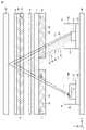
図3は、第1の実施形態における、LED21、受光素子34、OLEDパネル5、第1の円偏光板41、第2の円偏光板61、および第3の円偏光板51の配置を表わす図である。 FIG. 3 is a diagram showing the arrangement of the
スマートフォン100の長手方向をY軸方向とする。スマートフォン100の短手方向をX軸とする。スマートフォン100の正面の法線方向をZ軸方向とする。以下の説明では、下側とは、Z軸の負方向、上側とは、Z軸の正方向とする。 Let the longitudinal direction of the
第1の円偏光板41は、カバーパネル91の下側に配置される。具体的には、第1の円偏光板41は、カバーパネル91の下側の面に貼り付けられている。 The first
タッチパネル4は、第1の円偏光板41の下側に配置される。
OLEDパネル5は、タッチパネル4の下側に配置される。The
The
OLEDパネル5の下側に、メイン基板92上に発光部10と受光センサ98とを含む近接センサ9が配置される。 A proximity sensor 9 including a
発光部10は、発光モジュール196と、第2の円偏光板61とを備える。
発光モジュール196は、ベース基板94と、LED21と、樹脂体96とを備える。The
The
LED21は、ベース基板94上に配置される。樹脂体96は、LED21を水分および大気から保護する。ベース基板94の裏側の主面がメイン基板92の表側の主面PMと接続することによって、LED21は、メイン基板92と電気的に接続する。発光モジュール196の上側の面に第2の円偏光板61が貼り付けられている。すなわち、LED21の上側に、樹脂体96を介して第2の円偏光板61が配置される。 The
受光センサ98は、受光モジュール195と、第3の円偏光板51とを備える。受光モジュール195と、ベース基板93と、受光IC11と、樹脂体95とを備える。 The
受光IC11は、ベース基板93上に配置される。受光IC11は、受光素子34を含む。樹脂体95は、受光IC11を水分および大気から保護する。ベース基板93の裏側の主面がメイン基板92の表側の主面PMと接続することによって、受光IC11は、メイン基板92と電気的に接続する。受光モジュール195の上側の面に第3の円偏光板51が貼り付けられている。すなわち、受光素子34の上側に、樹脂体95を介して第3の円偏光板51が配置される。 The
第2の円偏光板61の偏光方向と第3の円偏光板51の偏光方向とは、同じである。第2の円偏光板61の偏光方向および第3の円偏光板51の偏光方向と、第1の円偏光板41の偏光方向とは、互いに逆向きである。 The polarization direction of the second
第1の円偏光板41は、第1の直線偏光板42と、第1の1/4波長板43とを備える。第1の1/4波長板43は、第1の直線偏光板42の下側に配置される。第1の直線偏光板42の透過軸をX軸方向とする。第1の直線偏光板42の透過軸(X軸)に対して、第1の1/4波長板43の光軸がα(=45度)の角度で交差する。 The first
第2の円偏光板61は、第2の直線偏光板63と、第2の1/4波長板62とを備える。第2の1/4波長板62は、第2の直線偏光板63の上側に配置される。第2の直線偏光板63の透過軸をX軸方向とする。第2の直線偏光板63の光軸と、第2の1/4波長板62の光軸とのなす角度はβ(=-45度)である。 The second
第3の円偏光板51は、第3の直線偏光板53と、第3の1/4波長板52とを備える。第3の1/4波長板52は、第3の直線偏光板53の上側に配置される。第3の直線偏光板53の透過軸をX軸方向とする。第3の直線偏光板53の光軸と、第3の1/4波長板52の光軸とのなす角度はβ(-45度)である。 The third
図4は、外部から入射される光の経路を表わす図である。
外部からの光は、カバーパネル91を経由して、第1の直線偏光板42に入射される。FIG. 4 is a diagram showing paths of light incident from the outside.
Light from the outside passes through the
第1の直線偏光板42からX軸方向に振動する光が出射されて、第1の1/4波長板43に入射される。 Light oscillating in the X-axis direction is emitted from the first linear
第1の1/4波長板43から第2の方向(左回り)に回転する光が出射されて、タッチパネル4を経て、OLEDパネル5に入射される。OLEDパネル5で反射された光は、タッチパネル4を経て、第1の1/4波長板43に入射される。 Light rotating in the second direction (counterclockwise) is emitted from the first quarter-
第1の1/4波長板43からは、2つの1/4波長板の位相差が加算されて、X軸方向と垂直方向に振動する光が出射されて、第1の直線偏光板42に入射される。第1の直線偏光板42は、入射された光を透過させない。これによって、外部から入射された光は、外部へ戻らない。これによって、OLEDパネル5のコントラストが低減されるのを防止できる。 From the first quarter-
図5は、LED21から出射された光の経路を表わす図である。
図5に示される光の経路(1)~(7)について説明する。FIG. 5 is a diagram showing paths of light emitted from the
The paths (1) to (7) of light shown in FIG. 5 will be described.
(1)経路(1)および(2)について
LED21から出射された光は、第2の直線偏光板63に入射される。第2の直線偏光板63からX軸方向に振動する光が出射されて、第2の1/4波長板62に入射される。第2の1/4波長板62から第1の方向(右回り)に回転する光が出射されて、OLEDパネル5およびタッチパネル4を経て、第1の1/4波長板43に入射される。第1の1/4波長板43からは、2つの1/4波長板の位相差が相殺されて、X軸方向に振動する光が出射されて、第1の直線偏光板42に入射される。(1) Routes (1) and (2) Light emitted from the
第1の直線偏光板42からX軸方向に振動する光が出射される。第1の直線偏光板42から出射されたX軸方向に振動する光は、カバーパネル91の上側の面で反射され(経路(2))、あるいは、カバーパネル91を経て、物体RFで反射される(経路(1))。反射されたX軸方向に振動する光は、カバーパネル91を経て、第1の直線偏光板42に入射される。第1の直線偏光板42からX軸方向に振動する光が出射されて、第1の1/4波長板43に入射される。 Light vibrating in the X-axis direction is emitted from the first linear
第1の1/4波長板43から第2の方向(左回り)に回転する光が出射されて、タッチパネル4およびOLEDパネル5を経て、第3の1/4波長板52に入射される。第3の1/4波長板52からは、2つの1/4波長板の位相差が相殺されて、X軸方向に振動する光が出射されて、第3の直線偏光板53に入射される。第3の直線偏光板53からX軸方向に振動する光が出射されて、受光素子34に入射される。これによって、経路(1)、(2)を辿った光は、受光素子34に入射される。図5では、経路(2)を辿る光は、物体RFによって反射されたものではないので、経路(2)を辿る光は、物体RFの近接の検出には、利用されない。しかし、物体RFがカバーパネル91に接触したときに、経路(2)がないと、物体RFの近接を検出することができなくなってしまう。したがって、経路(2)は、必要な経路である。また、物体RFが存在しないため、経路(1)を辿る光がない場合に、経路(2)を辿る光が受光素子34において検出される光の強度をI1とし、物体RFがカバーパネル91に接触したため、経路(1)を辿る光がない場合に、経路(2)を辿る光が受光素子34において検出される光の強度をI2としたときに、I2>I1となる。よって、物体RFがカバーパネル91に接触したときでも、物体RFの近接を検出することができる。 Light rotating in the second direction (counterclockwise) is emitted from the first quarter-
(2)経路(3)~(7)について
LED21から出射された光は、第2の直線偏光板63に入射される。第2の直線偏光板63からX軸方向に振動する光が出射されて、第2の1/4波長板62に入射される。第2の1/4波長板62から第1の方向(右回り)に回転する光が出射される。第2の1/4波長板62から出射された第1の方向(右回り)に回転する光は、第1の1/4波長板43の下側の面(経路(3))、タッチパネル4の上側の面(経路(4))、タッチパネル4の下側の面(経路(5))、OLEDパネル5の上側の面(経路(6))、OLEDパネル5の下側の面(経路(7))で反射される。反射された第1の方向(右回り)に回転する光は、第3の1/4波長板52に入射される。(2) Routes (3) to (7) Light emitted from the
第3の1/4波長板52からは、2つの1/4波長板の位相差が加算されて、X軸方向と垂直方向に振動する光が出射されて、第3の直線偏光板53に入射される。第3の直線偏光板53は、入射された光を透過させない。これによって、経路(3)を辿った光は、受光素子34に入射されない。よって、物体RFの近接の誤検出を防止できる。 The phase difference between the two quarter-wave plates is added from the third quarter-
以上のように、本実施の形態によれば、表示パネルとしてOLEDパネルを用い、OLEDパネルの下側に近接センサを配置することによって、ベゼルの面積を小さくすることができる。その結果、OLEDパネルの面積を大きくすることができる。 As described above, according to the present embodiment, the area of the bezel can be reduced by using the OLED panel as the display panel and arranging the proximity sensor below the OLED panel. As a result, the area of the OLED panel can be increased.
さらに、本実施の形態によれば、第1の円偏光板によって、外部からの光をOLEDパネルで反射されることがないようにすることができる。さらに、本実施の形態によれば、第1の円偏光板、第2の円偏光板、および第3の円偏光板によって、LEDから出射された光が内部のタッチパネル、OLEDパネルなどで反射されて受光素子に入射されることによって、物体の近接の検出精度が劣化するのを防止できる。 Furthermore, according to the present embodiment, the first circularly polarizing plate can prevent external light from being reflected by the OLED panel. Furthermore, according to the present embodiment, the light emitted from the LED is reflected by the touch panel, the OLED panel, etc. inside the first circular polarizer, the second circular polarizer, and the third circular polarizer. Therefore, it is possible to prevent the accuracy of detection of proximity of an object from deteriorating.
[第2の実施形態]
図6は、第2の実施形態における、LED21、受光素子34、OLEDパネル5、第1の円偏光板41、第2の円偏光板81、および第3の円偏光板71の配置を表わす図である。図6の第2の実施形態の配置が、図3の第1の実施形態の配置と相違する点は、以下である。[Second embodiment]
FIG. 6 is a diagram showing the arrangement of the
発光部10は、発光モジュール196の上面に貼り付けられた第2の円偏光板を備えない。受光センサ98は、受光モジュール195の上面に貼り付けられた第3の円偏光板を備えない。 The
第2の実施形態のスマートフォンは、LED21の上側であって、OLEDパネル5の下側の面に貼り付けられた第2の円偏光板81と、受光素子34の上側であって、OLEDパネル5の下側の面に貼り付けられた第3の円偏光板71とを備える。 The smartphone of the second embodiment includes a second
第2の円偏光板81の偏光方向と第3の円偏光板71の偏光方向とは、同じである。第2の円偏光板81の偏光方向および第3の円偏光板71の偏光方向と、第1の円偏光板41の偏光方向とは、互いに逆向きである。 The polarization direction of the second
第2の円偏光板81は、第2の直線偏光板83と、第2の1/4波長板82とを備える。第2の1/4波長板82は、第2の直線偏光板83の上側に配置される。第2の直線偏光板83の透過軸をX軸方向とする。第2の直線偏光板83の光軸と、第2の1/4波長板82の光軸とのなす角度はβ(=-45度)である。 The second
第3の円偏光板71は、第3の直線偏光板73と、第3の1/4波長板72とを備える。第3の1/4波長板72は、第3の直線偏光板73の上側に配置される。第3の直線偏光板73の透過軸をX軸方向とする。第3の直線偏光板73の光軸と、第3の1/4波長板72の光軸とのなす角度はβ(-45度)である。 The third
次に、図6に示される光の経路(1)~(7)について説明する。
(1)経路(1)および(2)について
LED21から出射された光は、第2の直線偏光板83に入射される。第2の直線偏光板83からX軸方向に振動する光が出射されて、第2の1/4波長板82に入射される。第2の1/4波長板82から第1の方向(右回り)に回転する光が出射されて、OLEDパネル5およびタッチパネル4を経て、第1の1/4波長板43に入射される。第1の1/4波長板43からは、2つの1/4波長板の位相差が相殺されて、X軸方向に振動する光が出射されて、第1の直線偏光板42に入射される。Next, the paths (1) to (7) of light shown in FIG. 6 will be described.
(1) Routes (1) and (2) Light emitted from the
第1の直線偏光板42からX軸方向に振動する光が出射される。第1の直線偏光板42から出射されたX軸方向に振動する光は、カバーパネル91の上側の面で反射され(経路(2))、あるいは、カバーパネル91を経て、物体RFで反射される(経路(1))。反射されたX軸方向に振動する光は、カバーパネル91を経て、第1の直線偏光板42に入射される。 Light vibrating in the X-axis direction is emitted from the first linear
第1の直線偏光板42からX軸方向に振動する光が出射されて、第1の1/4波長板43に入射される。第1の1/4波長板43から第2の方向(左回り)に回転する光が出射されて、タッチパネル4およびOLEDパネル5を経て、第3の1/4波長板72に入射される。第3の1/4波長板72からは、2つの1/4波長板の位相差が相殺されて、X軸方向に振動する光が出射されて、第3の直線偏光板73に入射される。第3の直線偏光板73からX軸方向に振動する光が出射されて、受光素子34に入射される。これによって、経路(1)、(2)を辿った光は、受光素子34に入射される。 Light oscillating in the X-axis direction is emitted from the first linear
(2)経路(3)~(7)について
LED21から出射された光は、第2の直線偏光板83に入射される。第2の直線偏光板83からX軸方向に振動する光が出射されて、第2の1/4波長板82に入射される。第2の1/4波長板82から第1の方向(右回り)に回転する光が出射される。第2の1/4波長板82から出射された第1の方向(右回り)に回転する光は、第1の1/4波長板43の下側の面(経路(3))、タッチパネル4の上側の面(経路(4))、タッチパネル4の下側の面(経路(5))、OLEDパネル5の上側の面(経路(6))、OLEDパネル5の下側の面(経路(7))で反射される。反射された第1の方向(右回り)に回転する光は、第3の1/4波長板72に入射される。(2) Routes (3) to (7) Light emitted from the
第3の1/4波長板72からは、2つの1/4波長板の位相差が加算されて、X軸方向と垂直方向に振動する光が出射されて、第3の直線偏光板73に入射される。第3の直線偏光板73は、入射された光を透過させない。これによって、経路(3)を辿った光は、受光素子34に入射されない。よって、物体RFの近接の誤検出を防止できる。 From the third quarter-
第2の実施形態でも、第1の実施形態と同様の効果が得られる。
[第3の実施形態]
図7は、第3の実施形態における、LED21、受光素子34、OLEDパネル5、第1の円偏光板41、第2の円偏光板81、および第3の円偏光板71の配置を表わす図である。The second embodiment also provides the same effects as the first embodiment.
[Third embodiment]
FIG. 7 is a diagram showing the arrangement of the
図7の第3の実施形態の配置が、図3の第1の実施形態の配置と相違する点は、以下である。第3の実施形態では、第1の円偏光板41、第2の円偏光板61、および第3の円偏光板51の代わりに、第1の円偏光板141、第2の円偏光板161、および第3の円偏光板151を備える。 The arrangement of the third embodiment of FIG. 7 differs from the arrangement of the first embodiment of FIG. 3 in the following. In the third embodiment, instead of the first
第1の円偏光板141は、カバーパネル91の下側に配置される。具体的には、第1の円偏光板141は、カバーパネル91の下側の面に貼り付けられている。 The first
発光モジュール196の上側の面に第2の円偏光板161が貼り付けられている。すなわち、LED21の上側に、樹脂体96を介して第2の円偏光板161が配置される。受光モジュール195の上側の面に第3の円偏光板151が貼り付けられている。すなわち、受光素子34の上側に、樹脂体95を介して第3の円偏光板151が配置される。 A second
第2の円偏光板161の偏光方向と第3の円偏光板151の偏光方向とは、同じである。第2の円偏光板161の偏光方向および第3の円偏光板151の偏光方向と、第1の円偏光板41の偏光方向とは、互いに逆向きである。 The polarization direction of the second
第1の円偏光板41は、第1の直線偏光板42と、第1の1/4波長板143とを備える。第1の1/4波長板143は、第1の直線偏光板42の下側に配置される。第1の直線偏光板42の透過軸をX軸方向とする。第1の直線偏光板42の透過軸(X軸)に対して、第1の1/4波長板143の光軸がα(=-45度)の角度で交差する。 The first
第2の円偏光板161は、第2の直線偏光板63と、第2の1/4波長板162とを備える。第2の1/4波長板162は、第2の直線偏光板63の上側に配置される。第2の直線偏光板63の透過軸をX軸方向とする。第2の直線偏光板63の光軸と、第2の1/4波長板162の光軸とのなす角度はβ(=45度)である。 The second
第3の円偏光板151は、第3の直線偏光板53と、第3の1/4波長板152とを備える。第3の1/4波長板152は、第3の直線偏光板53の上側に配置される。第3の直線偏光板53の透過軸をX軸方向とする。第3の直線偏光板53の光軸と、第3の1/4波長板152の光軸とのなす角度はβ(45度)である。 The third
図7に示される光の経路(1)~(7)について説明する。
(1)経路(1)および(2)について
LED21から出射された光は、第2の直線偏光板63に入射される。第2の直線偏光板63からX軸方向に振動する光が出射されて、第2の1/4波長板162に入射される。第2の1/4波長板162から第2の方向(左回り)に回転する光が出射されて、OLEDパネル5およびタッチパネル4を経て、第1の1/4波長板143に入射される。第1の1/4波長板143からは、2つの1/4波長板の位相差が相殺されて、X軸方向に振動する光が出射されて、第1の直線偏光板42に入射される。The paths (1) to (7) of light shown in FIG. 7 will be described.
(1) Routes (1) and (2) Light emitted from the
第1の直線偏光板42からX軸方向に振動する光が出射される。第1の直線偏光板42から出射されたX軸方向に振動する光は、カバーパネル91の上側の面で反射され(経路(2))、あるいは、カバーパネル91を経て、物体RFで反射される(経路(1))。反射されたX軸方向に振動する光は、カバーパネル91を経て、第1の直線偏光板42に入射される。 Light vibrating in the X-axis direction is emitted from the first linear
第1の直線偏光板42からX軸方向に振動する光が出射されて、第1の1/4波長板143に入射される。第1の1/4波長板143から第1の方向(右回り)に回転する光が出射されて、タッチパネル4およびOLEDパネル5を経て、第3の1/4波長板152に入射される。第3の1/4波長板152からは、2つの1/4波長板の位相差が相殺されて、X軸方向に振動する光が出射されて、第3の直線偏光板53に入射される。第3の直線偏光板53からX軸方向に振動する光が出射されて、受光素子34に入射される。これによって、経路(1)、(2)を辿った光は、受光素子34に入射される。これによって、経路(1)、(2)を辿った光は、受光素子34に入射される。 Light oscillating in the X-axis direction is emitted from the first linear
(2)経路(3)~(7)について
LED21から出射された光は、第2の直線偏光板63に入射される。第2の直線偏光板63からX軸方向に振動する光が出射されて、第2の1/4波長板162に入射される。第2の1/4波長板162から第2の方向(左回り)に回転する光が出射される。第2の1/4波長板162から出射された第2の方向(左回り)に回転する光は、第1の1/4波長板143の下側の面(経路(3))、タッチパネル4の上側の面(経路(4))、タッチパネル4の下側の面(経路(5))、OLEDパネル5の上側の面(経路(6))、OLEDパネル5の下側の面(経路(7))で反射される。反射された第2の方向(左回り)に回転する光は、第3の1/4波長板152に入射される。(2) Routes (3) to (7) Light emitted from the
第3の1/4波長板152からは、2つの1/4波長板の位相差が加算されて、X軸方向と垂直方向に振動する光が出射されて、第3の直線偏光板53に入射される。第3の直線偏光板53は、入射された光を透過させない。これによって、経路(3)~(7)を辿った光は、受光素子34に入射されない。よって、物体RFの近接の誤検出を防止できる。 From the third quarter-
第3の実施形態でも、第1の実施形態と同様の効果が得られる。
[第4の実施形態]
図8は、第4の実施形態における、LED21、受光素子34、OLEDパネル5、第1の円偏光板141、第2の円偏光板181、および第3の円偏光板171の配置を表わす図である。図8の第4の実施形態の配置が、図7の第3の実施形態の配置と相違する点は、以下である。The same effects as those of the first embodiment can be obtained in the third embodiment.
[Fourth embodiment]
FIG. 8 is a diagram showing the arrangement of the
発光部10は、発光モジュール196の上面に貼り付けられた第2の円偏光板を備えない。受光センサ98は、受光モジュール195の上面に貼り付けられた第3の円偏光板を備えない。 The
第4の実施形態のスマートフォンは、LED21の上側であって、OLEDパネル5の下側の面に貼り付けられた第2の円偏光板181と、受光素子34の上側であって、OLEDパネル5の下側の面に貼り付けられた第3の円偏光板171とを備える。 The smartphone of the fourth embodiment includes a second
第2の円偏光板181の偏光方向と第3の円偏光板171の偏光方向とは、同じである。第2の円偏光板181の偏光方向および第3の円偏光板171の偏光方向と、第1の円偏光板141の偏光方向とは、互いに逆向きである。 The polarization direction of the second
第2の円偏光板181は、第2の直線偏光板83と、第2の1/4波長板182とを備える。第2の1/4波長板182は、第2の直線偏光板83の上側に配置される。第2の直線偏光板83の透過軸をX軸方向とする。第2の直線偏光板83の光軸と、第2の1/4波長板182の光軸とのなす角度はβ(=45度)である。 The second
第3の円偏光板171は、第3の直線偏光板73と、第3の1/4波長板172とを備える。第3の1/4波長板172は、第3の直線偏光板73の上側に配置される。第3の直線偏光板73の透過軸をX軸方向とする。第3の直線偏光板73の光軸と、第3の1/4波長板172の光軸とのなす角度はβ(45度)である。 The third
図8に示される光の経路(1)~(7)について説明する。
(1)経路(1)および(2)について
LED21から出射された光は、第2の直線偏光板83に入射される。第2の直線偏光板83からX軸方向に振動する光が出射されて、第2の1/4波長板182に入射される。第2の1/4波長板182から第2の方向(左回り)に回転する光が出射されて、OLEDパネル5およびタッチパネル4を経て、第1の1/4波長板143に入射される。第1の1/4波長板143からは、2つの1/4波長板の位相差が相殺されて、X軸方向に振動する光が出射されて、第1の直線偏光板42に入射される。The paths (1) to (7) of light shown in FIG. 8 will be described.
(1) Routes (1) and (2) Light emitted from the
第1の直線偏光板42からX軸方向に振動する光が出射される。第1の直線偏光板42から出射されたX軸方向に振動する光は、カバーパネル91の上側の面で反射され(経路(2))、あるいは、カバーパネル91を経て、物体RFで反射される(経路(1))。反射されたX軸方向に振動する光は、カバーパネル91を経て、第1の直線偏光板42に入射される。 Light vibrating in the X-axis direction is emitted from the first linear
第1の直線偏光板42からX軸方向に振動する光が出射されて、第1の1/4波長板143に入射される。第1の1/4波長板143から第1の方向(右回り)に回転する光が出射されて、タッチパネル4およびOLEDパネル5を経て、第3の1/4波長板172に入射される。第3の1/4波長板172からは、2つの1/4波長板の位相差が相殺されて、X軸方向に振動する光が出射されて、第3の直線偏光板73に入射される。第3の直線偏光板73からX軸方向に振動する光が出射されて、受光素子34に入射される。これによって、経路(1)、(2)を辿った光は、受光素子34に入射される。 Light oscillating in the X-axis direction is emitted from the first linear
(2)経路(3)~(7)について
LED21から出射された光は、第2の直線偏光板83に入射される。第2の直線偏光板83からX軸方向に振動する光が出射されて、第2の1/4波長板182に入射される。第2の1/4波長板182から第2の方向(左回り)に回転する光が出射される。第2の1/4波長板182から出射された第2の方向(左回り)に回転する光は、第1の1/4波長板143の下側の面(経路(3))、タッチパネル4の上側の面(経路(4))、タッチパネル4の下側の面(経路(5))、OLEDパネル5の上側の面(経路(6))、OLEDパネル5の下側の面(経路(7))で反射される。反射された第2の方向(左回り)に回転する光は、第3の1/4波長板172に入射される。(2) Routes (3) to (7) Light emitted from the
第3の1/4波長板172からは、2つの1/4波長板の位相差が加算されて、X軸方向と垂直方向に振動する光が出射されて、第3の直線偏光板73に入射される。第3の直線偏光板73は、入射された光を透過させない。これによって、経路(3)を辿った光は、受光素子34に入射されない。よって、物体RFの近接の誤検出を防止できる。 From the third quarter-
第4の実施形態でも、第1の実施形態と同様の効果が得られる。
[第5の実施形態]
図9は、第5の実施形態における、LED21、受光素子34、OLEDパネル5、第1の円偏光板241、第2の円偏光板261、および第3の円偏光板251の配置を表わす図である。The fourth embodiment also provides the same effects as the first embodiment.
[Fifth embodiment]
FIG. 9 is a diagram showing the arrangement of the
図9の第5の実施形態の配置が、図3の第1の実施形態の配置と相違する点は、以下である。 The arrangement of the fifth embodiment in FIG. 9 differs from the arrangement of the first embodiment in FIG. 3 in the following.
第1の円偏光板241は、第1の1/4波長板43と第1の直線偏光板42との間に、第1の1/2波長板244を備える。第2の円偏光板261は、第2の1/4波長板62と第2の直線偏光板63との間に、第2の1/2波長板264を備える。第3の円偏光板251は、第3の1/4波長板52と第3の直線偏光板53との間に、第3の1/2波長板254を備える。 The first
1/4波長板43、62、53は、波長が短くなるほど、位相差が大きくなるという特性を有する。本実施の形態では、円偏光板241、261、251は、波長によって位相差が変化しないようにするために、1/2波長板244、264、254を備える。 The quarter-
1/2波長板244、264、254によって、光は180度回転するので、本実施の形態の光の経路(1)~(7)は、図5に示す第1の実施形態の光の経路と同様である。 Since the light is rotated 180 degrees by the half-
なお、第2~第4の実施形態のスマートフォンにおいても、同様に、第1、第2、および第3の円偏光板は、それぞれ、1/4波長板と直線偏光板との間に1/2波長板を備えるものとしてもよい。 In the smartphones of the second to fourth embodiments, similarly, the first, second, and third circularly polarizing plates each have a 1/4 wavelength between the quarter-wave plate and the linearly polarizing plate. A two-wave plate may be provided.
第5の実施形態でも、第1の実施形態と同様の効果が得られる。また、第5の実施形態では、3つの1/2波長板を追加することによって、物体の近接検出機能、外部からの光の反射防止機能の精度を高めることができる。 The fifth embodiment also provides the same effects as the first embodiment. In addition, in the fifth embodiment, by adding three half-wave plates, the accuracy of the object proximity detection function and the anti-reflection function of external light can be improved.
(変形例)
本発明は、上記の実施形態に限定されるものではなく、たとえば、以下のような変形例も含む。(Modification)
The present invention is not limited to the above embodiments, and includes, for example, the following modifications.
(1)上記の実施形態では、第1の直線偏光板の光軸と第1の1/4波長板の光軸とのなす角度は、45度または(-45)度であり、第2の直線偏光板の光軸と第2の1/4波長板の光軸とのなす角度は、(-45)度または45度であり、第3の直線偏光板の光軸と第3の1/4波長板の光軸とのなす角度は、(-45度)または45度としたが、これに限定されるものではない。 (1) In the above embodiment, the angle between the optical axis of the first linear polarizing plate and the optical axis of the first quarter-wave plate is 45 degrees or (−45) degrees, and the second The angle formed by the optical axis of the linear polarizing plate and the optical axis of the second quarter-wave plate is (−45) degrees or 45 degrees, and the optical axis of the third linear polarizing plate and the third 1/4 The angle formed by the four-wave plate with the optical axis was set to (−45 degrees) or 45 degrees, but is not limited to this.
第1の直線偏光板の光軸と第1の1/4波長板の光軸とのなす角度をαとし、第2の直線偏光板の光軸と第2の1/4波長板の光軸とのなす角度をβとし、第3の直線偏光板の光軸と第3の1/4波長板の光軸とのなす角度をβとし、αとβの大きさが等しく、αとβの符号が相違するものとしてもよい。 Let α be the angle between the optical axis of the first linear polarizing plate and the optical axis of the first quarter-wave plate, and the optical axis of the second linear polarizing plate and the optical axis of the second quarter-wave plate and β, the angle between the optical axis of the third linear polarizer and the optical axis of the third quarter-wave plate is β, and the magnitudes of α and β are equal, and between α and β They may have different signs.
αとβの大きさが45度のときには、1/4波長版に円偏光の光が入射または出射される。αとβの大きさが45度以外のときには、1/4波長版に楕円偏光の光が入射または出射される。 When the magnitudes of α and β are 45 degrees, circularly polarized light is incident on or emitted from the quarter-wave plate. When the magnitudes of α and β are other than 45 degrees, elliptically polarized light is incident on or emitted from the quarter-wave plate.
(2)上記の実施形態では、スマートフォンは、照度センサと、近接センサの受光センサとを備えるものとしたが、これに限定されるものではない。1つの受光センサが、照度検出と、近接検出の両方を実行するものとしてもよい。 (2) In the above embodiment, the smartphone includes the illuminance sensor and the light receiving sensor of the proximity sensor, but is not limited to this. A single light-receiving sensor may perform both illuminance detection and proximity detection.
(3)LEDの数は、1個に限定されるものではない。近接センサは、2個以上のLEDを備えるものとしてもよい。 (3) The number of LEDs is not limited to one. A proximity sensor may comprise more than one LED.
今回開示された実施の形態はすべての点で例示であって制限的なものではないと考えられるべきである。本発明の範囲は上記した説明ではなくて特許請求の範囲によって示され、特許請求の範囲と均等の意味および範囲内でのすべての変更が含まれることが意図される。 It should be considered that the embodiments disclosed this time are illustrative in all respects and not restrictive. The scope of the present invention is indicated by the scope of the claims rather than the above description, and is intended to include all modifications within the meaning and range of equivalents of the scope of the claims.
2 アンテナ、3 無線通信部、4 タッチパネル、5 OLEDパネル、6 照度センサ、7 スピーカ、8 マイク、9 近接センサ、10 発光部、11 受光IC、12 制御回路、13 プロセッサ、14 メモリ、15 電池、16 加速度センサ、17 ジャイロセンサ、21 LED、31 制御ロジック、32 パルス生成器、33 ドライバ、34 受光素子、35 アンプ、36 ADC、41,141,241 第1の円偏光板、61,81,161,181,261 第2の円偏光板、51,71,151,171,251 第3の円偏光板、42 第1の直線偏光板、63,83 第2の直線偏光板、53,73 第3の直線偏光板、43,143 第1の1/4波長板、62,82,162,182 第2の1/4波長板、52,72,152,172 第3の1/4波長板、91 カバーパネル、92 メイン基板、93,94 ベース基板、95,96 樹脂体、98 受光センサ、100 スマートフォン、195 受光モジュール、196 発光モジュール、244 第1の1/2波長板254 第3の1/2波長板、264 第2の1/2波長板、RF 物体。 2 antenna, 3 wireless communication unit, 4 touch panel, 5 OLED panel, 6 illuminance sensor, 7 speaker, 8 microphone, 9 proximity sensor, 10 light emitting unit, 11 light receiving IC, 12 control circuit, 13 processor, 14 memory, 15 battery, 16 acceleration sensor, 17 gyro sensor, 21 LED, 31 control logic, 32 pulse generator, 33 driver, 34 light receiving element, 35 amplifier, 36 ADC, 41,141,241 first circularly polarizing plate, 61,81,161 , 181, 261 second circularly polarizing plate, 51, 71, 151, 171, 251 third circularly polarizing plate, 42 first linearly polarizing plate, 63, 83 second linearly polarizing plate, 53, 73 third linear
Claims (8)
Translated fromJapanese前記電子機器は、カバーパネルと、前記カバーパネルの下側に配置された第1の円偏光板と、前記第1の円偏光板の下側に配置されたOLEDパネルと、前記OLEDパネルの下側に配置された発光部とを備え、前記発光部は、LEDと、前記LEDの上側に配置された第2の円偏光板とを含み、
前記受光センサは、
受光素子と、
前記受光素子の上側に配置された第3の円偏光板とを備え、
前記第2の円偏光板の偏光方向と前記第3の円偏光板の偏光方向とは、同じであり、
前記第2の円偏光板の偏光方向および前記第3の円偏光板の偏光方向と、前記第1の円偏光板の偏光方向とは、互いに逆向きである、受光センサ。A light receiving sensor mounted on an electronic device,
The electronic device includes a cover panel, a first circularly polarizing plate arranged below the cover panel, an OLED panel arranged below the first circularly polarizing plate, and below the OLED panel. a light emitting unit disposed on the side, the light emitting unit including an LED and a second circularly polarizing plate disposed above the LED;
The light receiving sensor is
a light receiving element;
A third circularly polarizing plate disposed above the light receiving element,
The polarization direction of the second circularly polarizing plate and the polarization direction of the third circularly polarizing plate are the same,
The light receiving sensor, wherein the polarization direction of the second circular polarizer and the polarization direction of the third circular polarizer and the polarization direction of the first circular polarizer are opposite to each other.
第1の直線偏光板と、
前記第1の直線偏光板の下側に配置された第1の1/4波長板とを含み、
前記第1の直線偏光板の透過軸に対して、前記第1の1/4波長板の光軸が角度αで交差し、
前記第2の円偏光板は、
第2の直線偏光板と、
前記第2の直線偏光板の上側に配置された第2の1/4波長板とを含み、
前記第2の直線偏光板の透過軸に対して、前記第2の1/4波長板の光軸が角度βで交差し、
前記第3の円偏光板は、
第3の直線偏光板と、
前記第3の直線偏光板の上側に配置された第3の1/4波長板とを含み、
前記第2の直線偏光板の透過軸に対して、前記第2の1/4波長板の光軸が角度βで交差し、
αとβの大きさが等しく、αとβの符号が相違する、請求項1記載の受光センサ。The first circularly polarizing plate is
a first linear polarizing plate;
a first quarter-wave plate disposed below the first linear polarizer;
the optical axis of the first quarter-wave plate intersects at an angle α with respect to the transmission axis of the first linear polarizer;
The second circularly polarizing plate is
a second linear polarizing plate;
a second quarter-wave plate disposed above the second linear polarizer;
the optical axis of the second quarter-wave plate intersects at an angle β with respect to the transmission axis of the second linear polarizer;
The third circularly polarizing plate is
a third linear polarizing plate;
a third quarter-wave plate disposed above the third linear polarizer;
the optical axis of the second quarter-wave plate intersects at an angle β with respect to the transmission axis of the second linear polarizer;
2. The light-receiving sensor according to claim 1, wherein [alpha] and [beta] have the same magnitude and [alpha] and [beta] have different signs.
前記第3の円偏光板は、前記受光素子が含まれるモジュールの上側の面に貼り付けられている、請求項1記載の受光センサ。The second circularly polarizing plate is attached to the upper surface of the module containing the LED,
2. The light receiving sensor according to claim 1, wherein said third circularly polarizing plate is attached to an upper surface of a module including said light receiving element.
前記電子機器は、カバーパネルと、前記カバーパネルの下側に配置された第1の円偏光板と、前記第1の円偏光板の下側に配置されたOLEDパネルとを備え、
前記近接センサは、
前記OLEDパネルの下側に配置された発光部と、
前記OLEDパネルの下側に配置された受光センサとを備え、
前記発光部は、
LEDと、
前記LEDの上側に配置された第2の円偏光板とを含み、
前記受光センサは、
受光素子と、
前記受光素子の上側に配置された第3の円偏光板とを含み、
前記第2の円偏光板の偏光方向と前記第3の円偏光板の偏光方向とは、同じであり、
前記第2の円偏光板の偏光方向および前記第3の円偏光板の偏光方向と、前記第1の円偏光板の偏光方向とは、互いに逆向きである、近接センサ。A proximity sensor mounted on an electronic device,
The electronic device comprises a cover panel, a first circularly polarizing plate arranged below the cover panel, and an OLED panel arranged below the first circularly polarizing plate,
The proximity sensor is
a light-emitting portion disposed below the OLED panel;
a light receiving sensor arranged on the lower side of the OLED panel,
The light emitting unit
an LED;
a second circularly polarizing plate disposed above the LED;
The light receiving sensor is
a light receiving element;
A third circularly polarizing plate disposed above the light receiving element,
The polarization direction of the second circularly polarizing plate and the polarization direction of the third circularly polarizing plate are the same,
The proximity sensor, wherein the polarization direction of the second circular polarizer, the polarization direction of the third circular polarizer, and the polarization direction of the first circular polarizer are opposite to each other.
前記カバーパネルの下側に配置された第1の円偏光板と、
前記第1の円偏光板の下側に配置されたOLEDパネルと、
前記OLEDパネルの下側に配置された発光部と、
前記OLEDパネルの下側に配置された受光センサとを備え、
前記発光部は、
LEDと、
前記LEDの上側に配置された第2の円偏光板とを含み、
前記受光センサは、
受光素子と、
前記受光素子の上側に配置された第3の円偏光板とを含み、
前記第1の円偏光板は、前記カバーパネルの下側の面に貼り付けられており、
前記第2の円偏光板は、前記LEDが含まれるモジュールの上側の面に貼り付けられており、
前記第3の円偏光板は、前記受光素子が含まれるモジュールの上側の面に貼り付けられており、
前記第2の円偏光板の偏光方向と前記第3の円偏光板の偏光方向とは、同じであり、
前記第2の円偏光板の偏光方向および前記第3の円偏光板の偏光方向と、前記第1の円偏光板の偏光方向とは、互いに逆向きである、電子機器。a cover panel;
a first circularly polarizing plate disposed under the cover panel;
an OLED panel disposed below the first circularly polarizing plate;
a light-emitting portion disposed below the OLED panel;
a light receiving sensor arranged on the lower side of the OLED panel,
The light emitting unit
an LED;
a second circularly polarizing plate disposed above the LED;
The light receiving sensor is
a light receiving element;
A third circularly polarizing plate disposed above the light receiving element,
The first circularly polarizing plate is attached to the lower surface of the cover panel,
The second circularly polarizing plate is attached to the upper surface of the module containing the LED,
The third circularly polarizing plate is attached to the upper surface of the module containing the light receiving element,
The polarization direction of the second circularly polarizing plate and the polarization direction of the third circularly polarizing plate are the same,
The electronic device, wherein the polarization direction of the second circular polarizer and the polarization direction of the third circular polarizer and the polarization direction of the first circular polarizer are opposite to each other.
カバーパネルと、
前記カバーパネルの下側に配置された第1の円偏光板と、
前記第1の円偏光板の下側に配置されたOLEDパネルと、
前記OLEDパネルの下側に配置された発光部と、
前記OLEDパネルの下側に配置された受光センサとを備え、
前記発光部は、LEDを含み、
前記受光センサは、受光素子を含み、
前記電子機器は、さらに、
前記LEDの上側に配置された第2の円偏光板と、
前記受光素子の上側に配置された第3の円偏光板とを備え、
前記第2の円偏光板は、前記OLEDパネルの下側の面に貼り付けられており、
前記第3の円偏光板は、前記OLEDパネルの下側の面に貼り付けられており、
前記第2の円偏光板の偏光方向と前記第3の円偏光板の偏光方向とは、同じであり、
前記第2の円偏光板の偏光方向および前記第3の円偏光板の偏光方向と、前記第1の円偏光板の偏光方向とは、互いに逆向きである、電子機器。an electronic device,
a cover panel;
a first circularly polarizing plate disposed under the cover panel;
an OLED panel disposed below the first circularly polarizing plate;
a light-emitting portion disposed below the OLED panel;
a light receiving sensor arranged on the lower side of the OLED panel,
The light emitting unit includes an LED,
The light receiving sensor includes a light receiving element,
The electronic device further comprises:
a second circularly polarizing plate disposed above the LED;
A third circularly polarizing plate disposed above the light receiving element,
The second circularly polarizing plate is attached to the lower surface of the OLED panel,
The third circularly polarizing plate is attached to the lower surface of the OLED panel,
The polarization direction of the second circularly polarizing plate and the polarization direction of the third circularly polarizing plate are the same,
The electronic device, wherein the polarization direction of the second circular polarizer and the polarization direction of the third circular polarizer and the polarization direction of the first circular polarizer are opposite to each other.
Priority Applications (1)
| Application Number | Priority Date | Filing Date | Title |
|---|---|---|---|
| JP2019089811AJP7209584B2 (en) | 2019-05-10 | 2019-05-10 | Light-receiving sensors, proximity sensors, and electronics |
Applications Claiming Priority (1)
| Application Number | Priority Date | Filing Date | Title |
|---|---|---|---|
| JP2019089811AJP7209584B2 (en) | 2019-05-10 | 2019-05-10 | Light-receiving sensors, proximity sensors, and electronics |
Publications (2)
| Publication Number | Publication Date |
|---|---|
| JP2020187847A JP2020187847A (en) | 2020-11-19 |
| JP7209584B2true JP7209584B2 (en) | 2023-01-20 |
Family
ID=73221942
Family Applications (1)
| Application Number | Title | Priority Date | Filing Date |
|---|---|---|---|
| JP2019089811AActiveJP7209584B2 (en) | 2019-05-10 | 2019-05-10 | Light-receiving sensors, proximity sensors, and electronics |
Country Status (1)
| Country | Link |
|---|---|
| JP (1) | JP7209584B2 (en) |
Cited By (1)
| Publication number | Priority date | Publication date | Assignee | Title |
|---|---|---|---|---|
| US20230033023A1 (en)* | 2020-11-29 | 2023-02-02 | Shlomo Zalman Reches | Detector locator system |
Citations (4)
| Publication number | Priority date | Publication date | Assignee | Title |
|---|---|---|---|---|
| JP2008112629A (en) | 2006-10-30 | 2008-05-15 | Omron Corp | Regressive reflection type photoelectric sensor, sensor body and regressive reflection part of regressive reflection type photoelectric sensor |
| JP2009169400A (en) | 2007-12-18 | 2009-07-30 | Sony Corp | Display and electronic apparatus |
| WO2010131387A1 (en) | 2009-05-15 | 2010-11-18 | シャープ株式会社 | Display apparatus |
| US20190294851A1 (en) | 2018-03-26 | 2019-09-26 | Samsung Electronics Co., Ltd. | Display panel for providing sensing light to optical fingerprint sensor and fingerprint sensing system including thereof |
- 2019
- 2019-05-10JPJP2019089811Apatent/JP7209584B2/enactiveActive
Patent Citations (4)
| Publication number | Priority date | Publication date | Assignee | Title |
|---|---|---|---|---|
| JP2008112629A (en) | 2006-10-30 | 2008-05-15 | Omron Corp | Regressive reflection type photoelectric sensor, sensor body and regressive reflection part of regressive reflection type photoelectric sensor |
| JP2009169400A (en) | 2007-12-18 | 2009-07-30 | Sony Corp | Display and electronic apparatus |
| WO2010131387A1 (en) | 2009-05-15 | 2010-11-18 | シャープ株式会社 | Display apparatus |
| US20190294851A1 (en) | 2018-03-26 | 2019-09-26 | Samsung Electronics Co., Ltd. | Display panel for providing sensing light to optical fingerprint sensor and fingerprint sensing system including thereof |
Cited By (2)
| Publication number | Priority date | Publication date | Assignee | Title |
|---|---|---|---|---|
| US20230033023A1 (en)* | 2020-11-29 | 2023-02-02 | Shlomo Zalman Reches | Detector locator system |
| US11681066B2 (en)* | 2020-11-29 | 2023-06-20 | Shlomo Zalman Reches | Detector locator system |
Also Published As
| Publication number | Publication date |
|---|---|
| JP2020187847A (en) | 2020-11-19 |
Similar Documents
| Publication | Publication Date | Title |
|---|---|---|
| KR102557031B1 (en) | Antenna module using metal bezel and electronic device including thereof | |
| USRE50466E1 (en) | Display device and mobile information terminal including the same | |
| KR102620548B1 (en) | Electronic device including a flexible circuit board on which a plurality of ground wirings surrounding signal wirings | |
| EP2909864B1 (en) | Electronic devices with display-integrated light sensors | |
| US9291495B2 (en) | Proximity sensor with combined light sensor having an increased viewing angle | |
| KR102763576B1 (en) | Electronic device incluidng optical sensor module | |
| US9046421B2 (en) | Light sensors for electronic devices | |
| KR20210012533A (en) | Electronic device including a shielding sheet and a heat radiation member | |
| US11435789B2 (en) | Electronic device having structure for connecting display and conductive support member through conductive adhesive member | |
| WO2019107862A1 (en) | Antenna and electronic device comprising same | |
| US11316266B2 (en) | Electronic device having structure for eliminating parasitic emission | |
| US12228967B2 (en) | Electronic device including photosensor module | |
| US11881617B2 (en) | Electronic device having flexible antenna disposed thereon | |
| JP7209584B2 (en) | Light-receiving sensors, proximity sensors, and electronics | |
| KR20190134361A (en) | Display including filling member separated from photo-curable member to form space through which light for photo-curing travels, and electronic device including the same | |
| US20210027682A1 (en) | Display device comprising wiring for detecting cracks formed on area adjacent to opening formed on display, and electronic device comprising same | |
| JP2015121544A (en) | Electronic apparatus | |
| US20130134303A1 (en) | Light sensing device having a lens | |
| US11227902B2 (en) | Light receiving IC, proximity sensor and electronic machine | |
| US20220276343A1 (en) | Light sensor | |
| KR102819148B1 (en) | Wearable electronic device and optical film for wearable electronic device | |
| JP2020177144A (en) | Electronic apparatus | |
| JP2005078433A (en) | Input coordinate detection system | |
| WO2017169607A1 (en) | Electronic device | |
| KR20240156912A (en) | Electronic device including distance measuring sensor |
Legal Events
| Date | Code | Title | Description |
|---|---|---|---|
| A621 | Written request for application examination | Free format text:JAPANESE INTERMEDIATE CODE: A621 Effective date:20220422 | |
| A977 | Report on retrieval | Free format text:JAPANESE INTERMEDIATE CODE: A971007 Effective date:20221208 | |
| TRDD | Decision of grant or rejection written | ||
| A01 | Written decision to grant a patent or to grant a registration (utility model) | Free format text:JAPANESE INTERMEDIATE CODE: A01 Effective date:20221220 | |
| A61 | First payment of annual fees (during grant procedure) | Free format text:JAPANESE INTERMEDIATE CODE: A61 Effective date:20230110 | |
| R150 | Certificate of patent or registration of utility model | Ref document number:7209584 Country of ref document:JP Free format text:JAPANESE INTERMEDIATE CODE: R150 |