JP7207406B2 - Display device - Google Patents
Display deviceDownload PDFInfo
- Publication number
- JP7207406B2 JP7207406B2JP2020519562AJP2020519562AJP7207406B2JP 7207406 B2JP7207406 B2JP 7207406B2JP 2020519562 AJP2020519562 AJP 2020519562AJP 2020519562 AJP2020519562 AJP 2020519562AJP 7207406 B2JP7207406 B2JP 7207406B2
- Authority
- JP
- Japan
- Prior art keywords
- light
- display device
- guide plate
- light guide
- optical device
- Prior art date
- Legal status (The legal status is an assumption and is not a legal conclusion. Google has not performed a legal analysis and makes no representation as to the accuracy of the status listed.)
- Active
Links
Images


Classifications
- G—PHYSICS
- G02—OPTICS
- G02B—OPTICAL ELEMENTS, SYSTEMS OR APPARATUS
- G02B27/00—Optical systems or apparatus not provided for by any of the groups G02B1/00 - G02B26/00, G02B30/00
- G02B27/01—Head-up displays
- G02B27/017—Head mounted
- G02B27/0172—Head mounted characterised by optical features
- G—PHYSICS
- G02—OPTICS
- G02B—OPTICAL ELEMENTS, SYSTEMS OR APPARATUS
- G02B27/00—Optical systems or apparatus not provided for by any of the groups G02B1/00 - G02B26/00, G02B30/00
- G02B27/01—Head-up displays
- G02B27/0101—Head-up displays characterised by optical features
- G02B27/0103—Head-up displays characterised by optical features comprising holographic elements
- G—PHYSICS
- G02—OPTICS
- G02B—OPTICAL ELEMENTS, SYSTEMS OR APPARATUS
- G02B27/00—Optical systems or apparatus not provided for by any of the groups G02B1/00 - G02B26/00, G02B30/00
- G02B27/01—Head-up displays
- G02B27/017—Head mounted
- G02B27/0176—Head mounted characterised by mechanical features
- G—PHYSICS
- G02—OPTICS
- G02B—OPTICAL ELEMENTS, SYSTEMS OR APPARATUS
- G02B27/00—Optical systems or apparatus not provided for by any of the groups G02B1/00 - G02B26/00, G02B30/00
- G02B27/28—Optical systems or apparatus not provided for by any of the groups G02B1/00 - G02B26/00, G02B30/00 for polarising
- G—PHYSICS
- G02—OPTICS
- G02B—OPTICAL ELEMENTS, SYSTEMS OR APPARATUS
- G02B27/00—Optical systems or apparatus not provided for by any of the groups G02B1/00 - G02B26/00, G02B30/00
- G02B27/42—Diffraction optics, i.e. systems including a diffractive element being designed for providing a diffractive effect
- G—PHYSICS
- G02—OPTICS
- G02B—OPTICAL ELEMENTS, SYSTEMS OR APPARATUS
- G02B5/00—Optical elements other than lenses
- G02B5/003—Light absorbing elements
- G—PHYSICS
- G02—OPTICS
- G02B—OPTICAL ELEMENTS, SYSTEMS OR APPARATUS
- G02B5/00—Optical elements other than lenses
- G02B5/18—Diffraction gratings
- G—PHYSICS
- G02—OPTICS
- G02C—SPECTACLES; SUNGLASSES OR GOGGLES INSOFAR AS THEY HAVE THE SAME FEATURES AS SPECTACLES; CONTACT LENSES
- G02C11/00—Non-optical adjuncts; Attachment thereof
- G02C11/10—Electronic devices other than hearing aids
- G—PHYSICS
- G02—OPTICS
- G02C—SPECTACLES; SUNGLASSES OR GOGGLES INSOFAR AS THEY HAVE THE SAME FEATURES AS SPECTACLES; CONTACT LENSES
- G02C5/00—Constructions of non-optical parts
- G02C5/12—Nose pads; Nose-engaging surfaces of bridges or rims
- G—PHYSICS
- G02—OPTICS
- G02C—SPECTACLES; SUNGLASSES OR GOGGLES INSOFAR AS THEY HAVE THE SAME FEATURES AS SPECTACLES; CONTACT LENSES
- G02C5/00—Constructions of non-optical parts
- G02C5/14—Side-members
- G—PHYSICS
- G02—OPTICS
- G02C—SPECTACLES; SUNGLASSES OR GOGGLES INSOFAR AS THEY HAVE THE SAME FEATURES AS SPECTACLES; CONTACT LENSES
- G02C5/00—Constructions of non-optical parts
- G02C5/22—Hinges
- G—PHYSICS
- G02—OPTICS
- G02F—OPTICAL DEVICES OR ARRANGEMENTS FOR THE CONTROL OF LIGHT BY MODIFICATION OF THE OPTICAL PROPERTIES OF THE MEDIA OF THE ELEMENTS INVOLVED THEREIN; NON-LINEAR OPTICS; FREQUENCY-CHANGING OF LIGHT; OPTICAL LOGIC ELEMENTS; OPTICAL ANALOGUE/DIGITAL CONVERTERS
- G02F1/00—Devices or arrangements for the control of the intensity, colour, phase, polarisation or direction of light arriving from an independent light source, e.g. switching, gating or modulating; Non-linear optics
- G02F1/01—Devices or arrangements for the control of the intensity, colour, phase, polarisation or direction of light arriving from an independent light source, e.g. switching, gating or modulating; Non-linear optics for the control of the intensity, phase, polarisation or colour
- G02F1/13—Devices or arrangements for the control of the intensity, colour, phase, polarisation or direction of light arriving from an independent light source, e.g. switching, gating or modulating; Non-linear optics for the control of the intensity, phase, polarisation or colour based on liquid crystals, e.g. single liquid crystal display cells
- G02F1/133—Constructional arrangements; Operation of liquid crystal cells; Circuit arrangements
- G02F1/1333—Constructional arrangements; Manufacturing methods
- G02F1/1335—Structural association of cells with optical devices, e.g. polarisers or reflectors
- G02F1/133509—Filters, e.g. light shielding masks
- G02F1/133512—Light shielding layers, e.g. black matrix
- G—PHYSICS
- G02—OPTICS
- G02F—OPTICAL DEVICES OR ARRANGEMENTS FOR THE CONTROL OF LIGHT BY MODIFICATION OF THE OPTICAL PROPERTIES OF THE MEDIA OF THE ELEMENTS INVOLVED THEREIN; NON-LINEAR OPTICS; FREQUENCY-CHANGING OF LIGHT; OPTICAL LOGIC ELEMENTS; OPTICAL ANALOGUE/DIGITAL CONVERTERS
- G02F1/00—Devices or arrangements for the control of the intensity, colour, phase, polarisation or direction of light arriving from an independent light source, e.g. switching, gating or modulating; Non-linear optics
- G02F1/01—Devices or arrangements for the control of the intensity, colour, phase, polarisation or direction of light arriving from an independent light source, e.g. switching, gating or modulating; Non-linear optics for the control of the intensity, phase, polarisation or colour
- G02F1/13—Devices or arrangements for the control of the intensity, colour, phase, polarisation or direction of light arriving from an independent light source, e.g. switching, gating or modulating; Non-linear optics for the control of the intensity, phase, polarisation or colour based on liquid crystals, e.g. single liquid crystal display cells
- G02F1/133—Constructional arrangements; Operation of liquid crystal cells; Circuit arrangements
- G02F1/1333—Constructional arrangements; Manufacturing methods
- G02F1/1335—Structural association of cells with optical devices, e.g. polarisers or reflectors
- G02F1/133524—Light-guides, e.g. fibre-optic bundles, louvered or jalousie light-guides
- G—PHYSICS
- G02—OPTICS
- G02F—OPTICAL DEVICES OR ARRANGEMENTS FOR THE CONTROL OF LIGHT BY MODIFICATION OF THE OPTICAL PROPERTIES OF THE MEDIA OF THE ELEMENTS INVOLVED THEREIN; NON-LINEAR OPTICS; FREQUENCY-CHANGING OF LIGHT; OPTICAL LOGIC ELEMENTS; OPTICAL ANALOGUE/DIGITAL CONVERTERS
- G02F1/00—Devices or arrangements for the control of the intensity, colour, phase, polarisation or direction of light arriving from an independent light source, e.g. switching, gating or modulating; Non-linear optics
- G02F1/01—Devices or arrangements for the control of the intensity, colour, phase, polarisation or direction of light arriving from an independent light source, e.g. switching, gating or modulating; Non-linear optics for the control of the intensity, phase, polarisation or colour
- G02F1/13—Devices or arrangements for the control of the intensity, colour, phase, polarisation or direction of light arriving from an independent light source, e.g. switching, gating or modulating; Non-linear optics for the control of the intensity, phase, polarisation or colour based on liquid crystals, e.g. single liquid crystal display cells
- G02F1/133—Constructional arrangements; Operation of liquid crystal cells; Circuit arrangements
- G02F1/1333—Constructional arrangements; Manufacturing methods
- G02F1/1335—Structural association of cells with optical devices, e.g. polarisers or reflectors
- G02F1/133528—Polarisers
- H—ELECTRICITY
- H04—ELECTRIC COMMUNICATION TECHNIQUE
- H04N—PICTORIAL COMMUNICATION, e.g. TELEVISION
- H04N5/00—Details of television systems
- H04N5/64—Constructional details of receivers, e.g. cabinets or dust covers
- G—PHYSICS
- G02—OPTICS
- G02B—OPTICAL ELEMENTS, SYSTEMS OR APPARATUS
- G02B27/00—Optical systems or apparatus not provided for by any of the groups G02B1/00 - G02B26/00, G02B30/00
- G02B27/01—Head-up displays
- G02B27/0101—Head-up displays characterised by optical features
- G02B2027/011—Head-up displays characterised by optical features comprising device for correcting geometrical aberrations, distortion
- G—PHYSICS
- G02—OPTICS
- G02B—OPTICAL ELEMENTS, SYSTEMS OR APPARATUS
- G02B27/00—Optical systems or apparatus not provided for by any of the groups G02B1/00 - G02B26/00, G02B30/00
- G02B27/01—Head-up displays
- G02B27/0101—Head-up displays characterised by optical features
- G02B2027/0118—Head-up displays characterised by optical features comprising devices for improving the contrast of the display / brillance control visibility
- G—PHYSICS
- G02—OPTICS
- G02B—OPTICAL ELEMENTS, SYSTEMS OR APPARATUS
- G02B27/00—Optical systems or apparatus not provided for by any of the groups G02B1/00 - G02B26/00, G02B30/00
- G02B27/01—Head-up displays
- G02B27/0101—Head-up displays characterised by optical features
- G02B2027/014—Head-up displays characterised by optical features comprising information/image processing systems
- G—PHYSICS
- G02—OPTICS
- G02B—OPTICAL ELEMENTS, SYSTEMS OR APPARATUS
- G02B27/00—Optical systems or apparatus not provided for by any of the groups G02B1/00 - G02B26/00, G02B30/00
- G02B27/01—Head-up displays
- G02B27/0149—Head-up displays characterised by mechanical features
- G02B2027/0154—Head-up displays characterised by mechanical features with movable elements
- G02B2027/0158—Head-up displays characterised by mechanical features with movable elements with adjustable nose pad
- G—PHYSICS
- G02—OPTICS
- G02B—OPTICAL ELEMENTS, SYSTEMS OR APPARATUS
- G02B27/00—Optical systems or apparatus not provided for by any of the groups G02B1/00 - G02B26/00, G02B30/00
- G02B27/01—Head-up displays
- G02B27/017—Head mounted
- G02B2027/0178—Eyeglass type
- G—PHYSICS
- G02—OPTICS
- G02F—OPTICAL DEVICES OR ARRANGEMENTS FOR THE CONTROL OF LIGHT BY MODIFICATION OF THE OPTICAL PROPERTIES OF THE MEDIA OF THE ELEMENTS INVOLVED THEREIN; NON-LINEAR OPTICS; FREQUENCY-CHANGING OF LIGHT; OPTICAL LOGIC ELEMENTS; OPTICAL ANALOGUE/DIGITAL CONVERTERS
- G02F2203/00—Function characteristic
- G02F2203/12—Function characteristic spatial light modulator
Landscapes
- Physics & Mathematics (AREA)
- Optics & Photonics (AREA)
- General Physics & Mathematics (AREA)
- Nonlinear Science (AREA)
- Health & Medical Sciences (AREA)
- Ophthalmology & Optometry (AREA)
- Mathematical Physics (AREA)
- Crystallography & Structural Chemistry (AREA)
- Chemical & Material Sciences (AREA)
- Engineering & Computer Science (AREA)
- Signal Processing (AREA)
- Multimedia (AREA)
- Acoustics & Sound (AREA)
- General Health & Medical Sciences (AREA)
- Otolaryngology (AREA)
- Electrochromic Elements, Electrophoresis, Or Variable Reflection Or Absorption Elements (AREA)
- Liquid Crystal (AREA)
Description
Translated fromJapanese本開示は、表示装置に関し、より具体的には、頭部装着型ディスプレイ(HMD,Head Mounted Display)に用いられる表示装置に関する。 TECHNICAL FIELD The present disclosure relates to a display device, and more specifically to a display device used for a head mounted display (HMD).
近年、現実の環境(あるいはその一部)に付加情報としてバーチャルな物体や各種情報を電子情報として合成・提示する拡張現実技術(AR技術:Augmented Reality)が、注目を浴びている。この拡張現実技術を実現するために、視覚情報を提示する装置として、例えば、頭部装着型ディスプレイが検討されている。そして、応用分野として、現実の環境における作業支援が期待されており、例えば、道路案内情報の提供、メンテナンス等を行う技術者に対する技術情報提供等を挙げることができる。特に、頭部装着型ディスプレイは、手がふさがられることがないため、非常に便利である。また、屋外を移動しながら各種情報等を得る場合にも、視界に映像あるいは画像から構成された各種情報等と外部環境とを同時に捉えることができるため、スムーズな移動が可能となる。 In recent years, augmented reality technology (AR technology) that synthesizes and presents virtual objects and various types of information as electronic information as additional information in a real environment (or a part thereof) has attracted attention. In order to realize this augmented reality technology, for example, a head-mounted display is being considered as a device for presenting visual information. As an application field, work support in a real environment is expected. In particular, head-mounted displays are very convenient because they keep your hands free. In addition, even when obtaining various information while moving outdoors, the external environment can be grasped simultaneously with the various information composed of video or images in the field of view, so smooth movement becomes possible.
画像形成装置によって形成された2次元画像を虚像光学系により拡大虚像として観察者に観察させるための虚像表示装置(表示装置)が、例えば、特開2014-219468号公報から周知である。 A virtual image display device (display device) for allowing an observer to observe a two-dimensional image formed by an image forming apparatus as an enlarged virtual image using a virtual image optical system is known from, for example, Japanese Patent Laid-Open No. 2014-219468.
特開2014-219468号公報に開示された虚像表示装置において、導光装置(光学部材)20の周囲部分のうち、フレーム107に近い上辺側には、フレーム107の下面に設けられた制限部107nに嵌め込まれるリブ10nが形成されており、このリブ10nの存在により、導光装置20の奥行き方向(Z方向)に関する変位が制限される(特開2014-219468号公報の段落番号[0046]参照)。そして、導光装置20は、フレーム107のネック部に形成された突起状の取付部10gを利用して、フレーム107の側方端部65aに設けた第2固定部61eに直接固定されており、ネジ孔61uを介してネジ61vをネジ孔10uにねじ込むことでフレーム107に対して着脱可能に固定される(特開2014-219468号公報の段落番号[0047]参照)。また、フレーム107及びプロテクター108が、第1及び第2像形成本体部105a,105bに連結された根元側を除いた導光装置20の長円状の周囲部分と離間するか又は緩く接しており、導光装置20と、フレーム107及びプロテクター108を含む枠部102との間に熱膨張率の差があっても、枠部102内での導光装置20の膨張が許容され、導光装置20に歪み、変形、破損が生じることを防止できる(特開2014-219468号公報の段落番号[0028]参照)。 In the virtual image display device disclosed in Japanese Patent Application Laid-Open No. 2014-219468, a limiting portion 107n provided on the lower surface of the frame 107 is provided on the upper side near the frame 107 in the peripheral portion of the light guide device (optical member) 20. Due to the presence of the rib 10n, the displacement of the
以上のとおり、特開2014-219468号公報に開示された虚像表示装置において、導光装置(光学部材)20の周囲部分のうち、フレーム107に近い上辺側には、フレーム107の下面に設けられた制限部107nに嵌め込まれるリブ10nが形成されているし、耳側の導光装置20の部分は、ネジ61vによってフレーム107に固定されている。また、フレーム107及びプロテクター108は、鼻側の導光装置20の部分と離間するか又は緩く接しており、導光装置20と、フレーム107及びプロテクター108を含む枠部102との間に熱膨張率の差があっても、枠部102内での導光装置20の膨張が許容される。 As described above, in the virtual image display device disclosed in Japanese Patent Application Laid-Open No. 2014-219468, the upper side near the frame 107 in the peripheral portion of the light guide device (optical member) 20 is provided on the lower surface of the frame 107. A rib 10n is formed to be fitted into the restricting portion 107n, and the portion of the
ところで、上述した従来の表示装置(虚像表示装置)において、観察者に依存して、観察者が表示装置を頭部に装着したとき、テンプル部104が外側に広がる場合がある。その結果、このような場合、フレーム107の正面部107aに応力が加わり、テンプル部104と鼻受部40との間のフレーム107の正面部107aの領域が歪んでしまう。フレーム107の正面部107aのこのような領域に歪みが生じると、導光装置(光学部材)20は、その周囲部分がフレーム107の下面に設けられた制限部107nに嵌め込まれているので、導光装置20にも歪みが生じる。また、フレーム107及びプロテクター108と離間するか又は緩く接している鼻側の導光装置20の部分が、フレーム107及びプロテクター108に強く接するようになり、導光装置20に一層の歪みが生じる。そして、導光装置20に歪みが生じると、観察者が観察する画像にも歪みが発生する。また、導光装置20の鼻側端部はプロテクター108と接しているだけなので、観察者の頭上に太陽が位置し、太陽光が、直接、導光装置20の鼻側の部分の端面に入射した場合、導光装置20の内部で迷光が発生し、画像の品質低下を招くといった問題もある。 By the way, in the conventional display device (virtual image display device) described above, depending on the observer, when the observer wears the display device on the head, the temple portion 104 may expand outward. As a result, in such a case, stress is applied to the front portion 107a of the frame 107, and the area of the front portion 107a of the frame 107 between the temple portion 104 and the
従って、本開示の第1の目的は、太陽光が、直接、光学装置(導光装置)を照射した場合であっても、画像の品質低下が生じ難い構成、構造を有する表示装置を提供することにある。また、本開示の第2の目的は、観察者に依存して、観察者が表示装置を頭部に装着したときテンプル部が外側に広がった場合であっても、観察者が観察する画像の画質への影響が少ない構成、構造を有する表示装置を提供することにある。 Accordingly, a first object of the present disclosure is to provide a display device having a configuration and a structure in which deterioration of image quality is unlikely to occur even when sunlight directly irradiates an optical device (light guide device). That's what it is. A second object of the present disclosure is to improve the image observed by the observer even when the temple portion expands outward when the observer wears the display device on the head. An object of the present invention is to provide a display device having a configuration and structure that have little influence on image quality.
上記の第1の目的及び第2の目的を達成するための本開示の第1の態様及び第2の態様に係る表示装置は、
観察者の正面に配置されるフロント部、フロント部の両端から延びるテンプル部、及び、パッド部を備え、観察者の頭部に装着されるフレーム、並びに、
フレームに取り付けられた画像表示装置、
を備えた表示装置であって、
画像表示装置は、
画像形成装置、及び、
画像形成装置から出射された光が入射され、観察者に向かって出射する光学装置、
を備えており、
光学装置の一端部は、フロント部のテンプル部側に固定されている。The display device according to the first and second aspects of the present disclosure for achieving the first and second objects described above comprises:
a frame to be worn on the head of the observer, comprising a front portion arranged in front of the observer, temple portions extending from both ends of the front portion, and a pad portion;
an image display device mounted on a frame;
A display device comprising
The image display device
an image forming apparatus, and
an optical device into which light emitted from an image forming device is incident and emitted toward an observer;
and
One end of the optical device is fixed to the temple portion side of the front portion.
そして、本開示の第1の態様に係る表示装置において、光学装置の他端部は、フロント部のパッド部側に配置されており、光学装置の他端部の上方から光学装置の他端部への外光の入射を防ぐ遮光部材が、フロント部のパッド部側に取り付けられている。 Further, in the display device according to the first aspect of the present disclosure, the other end portion of the optical device is arranged on the pad portion side of the front portion, and the other end portion of the optical device can be seen from above the other end portion of the optical device. A light shielding member for preventing external light from entering the front portion is attached to the pad portion side of the front portion.
また、本開示の第2の態様に係る表示装置において、光学装置の他端部は、フロント部のパッド部側に配置され、フロント部において自在に滑動する。 Further, in the display device according to the second aspect of the present disclosure, the other end portion of the optical device is arranged on the pad portion side of the front portion and freely slides on the front portion.
以下、図面を参照して、実施例に基づき本開示を説明するが、本開示は実施例に限定されるものではなく、実施例における種々の数値や材料は例示である。尚、説明は、以下の順序で行う。
1.本開示の第1の態様~第2の態様に係る表示装置、全般に関する説明
2.実施例1(本開示の第1の態様に係る表示装置)
3.実施例2(本開示の第2の態様に係る表示装置)
4.実施例3(実施例1~実施例2の表示装置を構成する画像表示装置及び光学装置)
5.実施例4(実施例3の変形)
6.実施例5(実施例3~実施例4の変形)
7.実施例6(実施例1~実施例4の別の変形、調光装置)
8.その他Hereinafter, the present disclosure will be described based on examples with reference to the drawings, but the present disclosure is not limited to the examples, and various numerical values and materials in the examples are examples. The description will be made in the following order.
1. General description of the display device according to the first and second aspects of the present disclosure2. Example 1 (display device according to the first aspect of the present disclosure)
3. Example 2 (display device according to the second aspect of the present disclosure)
4. Example 3 (Image display device and optical device constituting the display device of Examples 1 and 2)
5. Example 4 (Modification of Example 3)
6. Example 5 (Modifications of Examples 3 and 4)
7. Example 6 (Another modification of Examples 1 to 4, light control device)
8. others
〈本開示の第1の態様~第2の態様に係る表示装置、全般に関する説明〉
本開示の第1の態様に係る表示装置において、光学装置の他端部は、観察者と対向する遮光部材の対向面の上を自在に滑動する形態とすることができる。あるいは又、光学装置の他端部は、観察者と対向する遮光部材の対向面と接しない形態とすることができる。<General Description of Display Devices According to First and Second Aspects of Present Disclosure>
In the display device according to the first aspect of the present disclosure, the other end portion of the optical device can be configured to freely slide on the facing surface of the light shielding member that faces the viewer. Alternatively, the other end of the optical device may be configured so as not to contact the surface of the light blocking member that faces the viewer.
本開示の第2の態様に係る表示装置において、フロント部のパッド部側には、光学装置受け部材が取り付けられており、光学装置の他端部は、光学装置受け部材の上を自在に滑動する形態とすることができる。そして、この場合、
光学装置受け部材は、仮想水平面で切断したときの断面形状がL字の部材から成り、
L字の縦棒の部分に相当する光学装置受け部材の第1の部分は、観察者と対向して垂直方向に延びており、
観察者から遠い方の光学装置受け部材の第1の部分の端部から延びるL字の横棒の部分に相当する光学装置受け部材の第2の部分は、フロント部のテンプル部側に向かって延びており、
光学装置の他端部は、光学装置受け部材の第2の部分の観察者と対向する対向面の上を自在に滑動する形態とすることができる。あるいは又、光学装置受け部材は、観察者と対向して垂直方向に延びる棒状あるいは面状の部材から成り、光学装置の他端部は、棒状あるいは面状の部材から成る光学装置受け部材の観察者と対向する対向面の上を自在に滑動する形態とすることができる。尚、「垂直方向の延びる」状態には、厳密に垂直方向の延びる状態だけでなく、若干、垂直方向からずれて延びる状態も包含される。In the display device according to the second aspect of the present disclosure, the optical device receiving member is attached to the pad portion side of the front portion, and the other end portion of the optical device freely slides on the optical device receiving member. It can be in the form of And in this case,
The optical device receiving member is made of a member having an L-shaped cross section when cut along an imaginary horizontal plane,
a first portion of the optical device receiving member corresponding to the portion of the L-shaped vertical bar extends vertically facing the viewer;
The second portion of the optical device receiving member corresponding to the portion of the L-shaped horizontal bar extending from the end of the first portion of the optical device receiving member farther from the observer is directed toward the temple portion of the front portion. is extended,
The other end of the optical device may be configured to freely slide over the facing surface of the second portion of the optical device receiving member facing the viewer. Alternatively, the optical device receiving member may be a rod-shaped or planar member extending vertically facing the observer, and the other end of the optical device may be a rod-shaped or planar member. It can be configured to freely slide on the facing surface facing the person. It should be noted that the state of "extending in the vertical direction" includes not only the state of extending in the strictly vertical direction, but also the state of extending slightly out of the vertical direction.
以上に説明した好ましい形態を含む本開示の第1の態様~第2の態様に係る表示装置において、光学装置の一端部は、限定するものではないが、フロント部のテンプル部側に配設された画像形成装置に取り付けられている形態とすることができる。具体的には、例えば、光学装置の一端部を、画像形成装置に、接着剤を用いて取り付け、あるいは又、ビスを用いて取り付ければよい。 In the display devices according to the first to second aspects of the present disclosure including the preferred embodiments described above, one end of the optical device is, but not limited to, disposed on the temple portion side of the front portion. It can be installed in an image forming apparatus. Specifically, for example, one end of the optical device may be attached to the image forming apparatus using an adhesive, or may be attached using screws.
更には、以上に説明した好ましい形態を含む本開示の第1の態様~第2の態様に係る表示装置において、光学装置は、
画像形成装置から入射された光が内部を全反射により伝播した後、観察者に向けて出射される導光板、
導光板に入射された光が導光板の内部で全反射されるように、導光板に入射された光を偏向させる第1偏向手段、及び、
導光板の内部を全反射により伝播した光を導光板から出射させるために、導光板の内部を全反射により伝播した光を偏向させる第2偏向手段、
を備えている形態とすることができる。尚、「全反射」という用語は、内部全反射、あるいは、導光板内部における全反射を意味する。画像形成装置から入射された光は、導光板の内部を全反射により伝播した後、観察者に向けて出射されるし、第2偏向手段によって光学装置の虚像形成領域が構成される。Furthermore, in the display devices according to the first and second aspects of the present disclosure, including the preferred modes described above, the optical device is
a light guide plate in which light incident from an image forming apparatus is emitted toward an observer after being propagated by total internal reflection;
a first deflection means for deflecting light incident on the light guide plate so that the light incident on the light guide plate is totally reflected inside the light guide plate;
second deflection means for deflecting the light propagated through the light guide plate by total reflection so that the light propagated inside the light guide plate by total reflection is emitted from the light guide plate;
can be in the form of The term "total reflection" means total internal reflection or total reflection inside the light guide plate. Light incident from the image forming apparatus propagates through the interior of the light guide plate by total reflection, and is emitted toward the observer, and the second deflection means constitutes the virtual image forming area of the optical apparatus.
更には、以上に説明した好ましい形態を含む本開示の第1の態様~第2の態様に係る表示装置において、画像形成装置は、フロント部のテンプル部側に取り付けられている形態とすることができる。具体的には、画像形成装置を内部に格納した筐体を、テンプル部側のフロント部に取り付ければよいし、あるいは又、テンプル部に取り付ければよいし、テンプル部側のフロント部からテンプル部に亙り取り付ければよい。画像形成装置の取付け(筐体の取付け)は、例えば、ビスを用いる方法等、適切な方法によって行えばよい。 Furthermore, in the display device according to the first aspect to the second aspect of the present disclosure including the preferred aspects described above, the image forming device may be attached to the temple portion side of the front portion. can. Specifically, the housing in which the image forming apparatus is stored may be attached to the front portion on the side of the temple portion, or may be attached to the temple portion. All you have to do is install it. Attachment of the image forming apparatus (attachment of the housing) may be performed by an appropriate method such as a method using screws.
更には、以上に説明した好ましい形態を含む本開示の第1の態様~第2の態様に係る表示装置において、光学装置は、更に、外部から入射する外光の光量を調整する調光装置を備えている形態とすることができる。調光装置に関しては、実施例6において、詳しく説明する。 Furthermore, in the display devices according to the first and second aspects of the present disclosure including the preferred embodiments described above, the optical device further includes a light control device that adjusts the amount of external light incident from the outside. It can be in the form of having A dimmer will be described in detail in a sixth embodiment.
遮光部材は、不透明な種々のプラスチック材料や金属材料、合金材料から作製すればよいし、フロント部のパッド部側への遮光部材の取付けは、接着剤を用いる方法、ビスを用いる方法等、適切な方法を採用すればよい。遮光部材は、具体的には、パッド部側のフロント部の部分に取り付けてもよいし、パッド部に取り付けてもよいし、遮光部材がフロント部と一体となった構造とすることもできるし、遮光部材がパッド部と一体となった構造とすることもできる。遮光部材がフロント部と一体となった構造や遮光部材がパッド部と一体となった構造も、「遮光部材がフロント部のパッド部側に取り付けられている」構造に包含される。導光板の上方に位置する遮光部材の部分の長さは、導光板の軸線(長手方向、水平方向であり、X軸方向に該当する)の長さの10%乃至100%とすることが好ましいが、これに限定するものではない。 The light-shielding member may be made of various opaque plastic materials, metal materials, or alloy materials, and the light-shielding member may be attached to the pad portion side of the front portion by an appropriate method such as a method using an adhesive or a method using screws. method should be adopted. Specifically, the light shielding member may be attached to the front portion on the side of the pad portion, may be attached to the pad portion, or may have a structure in which the light shielding member is integrated with the front portion. Alternatively, the light shielding member may be integrated with the pad portion. A structure in which the light shielding member is integrated with the front portion and a structure in which the light shielding member is integrated with the pad portion are also included in the structure in which the light shielding member is attached to the pad portion side of the front portion. The length of the portion of the light shielding member located above the light guide plate is preferably 10% to 100% of the length of the axis of the light guide plate (longitudinal direction, horizontal direction, corresponding to the X-axis direction). However, it is not limited to this.
光学装置受け部材は、不透明な種々のプラスチック材料や金属材料、合金材料から作製すればよいし、フロント部のパッド部側への光学装置受け部材の取付けは、接着剤を用いる方法、ビスを用いる方法等、適切な方法を採用すればよい。光学装置受け部材は、具体的には、パッド部側のフロント部の部分に取り付けてもよいし、パッド部に取り付けてもよいし、光学装置受け部材がフロント部と一体となった構造とすることもできるし、光学装置受け部材がパッド部と一体となった構造とすることもできる。導光板に対向する光学装置受け部材の部分の長さは、導光板の幅方向(高さ方向、垂直方向であり、Y軸方向に該当する)の長さの20%乃至100%とすることが好ましいが、これに限定するものではない。 The optical device receiving member may be made of various opaque plastic materials, metal materials, and alloy materials, and the optical device receiving member is attached to the pad portion side of the front portion by a method using an adhesive or by using screws. An appropriate method such as a method may be adopted. Specifically, the optical device receiving member may be attached to the front portion on the side of the pad portion, or may be attached to the pad portion, and the optical device receiving member may be integrated with the front portion. Alternatively, a structure in which the optical device receiving member is integrated with the pad portion may be employed. The length of the portion of the optical device receiving member that faces the light guide plate should be 20% to 100% of the length in the width direction of the light guide plate (height direction, vertical direction, corresponding to the Y-axis direction). is preferred, but not limited to this.
以上に説明した各種の好ましい形態、構成を含む本開示の第1の態様~第2の態様に係る表示装置(以下、これらを総称して、『本開示の表示装置等』と呼ぶ場合がある)において、2つのテンプル部のそれぞれは、フロント部の両端に蝶番を介して回動自在に取り付けられた構成とすることができるし、フロント部と2つのテンプル部とが一体となった構成とすることもできる。各テンプル部の先端部には、必要に応じて、モダン部(先セル部)が取り付けられている。パッド部はフロント部に取り付けられている形態とすることもできる。本開示の表示装置等の全体を眺めたとき、フレームは、概ね通常の眼鏡やサングラスと略同じ外観である。パッド部を含むフレームを構成する材料は、金属や合金、プラスチック、これらの組合せといった、通常の眼鏡やサングラスを構成する材料と同じ材料から構成することができる。テンプル部にスピーカやヘッドホンを取り付けてもよいし、フロント部に撮像装置を取り付けてもよい。 Display devices according to the first and second aspects of the present disclosure, including the various preferred forms and configurations described above (hereinafter collectively referred to as "display devices of the present disclosure, etc." ), each of the two temple portions can be configured to be rotatably attached to both ends of the front portion via hinges, or the front portion and the two temple portions can be integrated. You can also A modern part (preceding cell part) is attached to the tip part of each temple part, if necessary. The pad portion may be attached to the front portion. When viewing the display device or the like of the present disclosure as a whole, the frame has substantially the same appearance as ordinary eyeglasses or sunglasses. The material constituting the frame including the pad portion can be composed of the same materials as those constituting ordinary spectacles and sunglasses, such as metals, alloys, plastics, and combinations thereof. A speaker or headphones may be attached to the temple portion, or an imaging device may be attached to the front portion.
以上に説明した各種好ましい形態、構成を含む本開示の表示装置等において、第1偏向手段及び第2偏向手段は、ホログラム回折格子膜から構成されている形態とすることができる。 In the display device and the like of the present disclosure including the various preferred forms and configurations described above, the first deflecting means and the second deflecting means can be configured with a hologram diffraction grating film.
第1偏向手段及び第2偏向手段がホログラム回折格子膜から構成されている場合、第1偏向手段は、導光板に入射された光を回折反射し、第2偏向手段は、導光板の内部を全反射により伝播した光を回折反射する。ホログラム回折格子膜は、反射型のホログラム回折格子膜から成る構成とすることができるし、あるいは又、透過型のホログラム回折格子膜から成る構成とすることができるし、あるいは又、一方のホログラム回折格子膜は反射型のホログラム回折格子膜から成り、他方のホログラム回折格子膜は透過型のホログラム回折格子膜から成る構成とすることができる。反射型のホログラム回折格子膜として、反射型の体積ホログラム回折格子膜を挙げることができる。反射型の体積ホログラム回折格子膜から成る第1偏向手段を、便宜上、『第1回折格子部材』と呼び、反射型の体積ホログラム回折格子膜から成る第2偏向手段を、便宜上、『第2回折格子部材』と呼ぶ場合がある。 When the first deflecting means and the second deflecting means are composed of a holographic diffraction grating film, the first deflecting means diffracts and reflects the light incident on the light guide plate, and the second deflecting means diffracts and reflects the inside of the light guide plate. It diffracts and reflects the light propagated by total reflection. The hologram diffraction grating film can be composed of a reflection-type hologram diffraction grating film, or can be composed of a transmission-type hologram diffraction grating film, or alternatively, can be composed of one hologram diffraction grating film. The grating film may be a reflective holographic diffraction grating film, and the other holographic diffraction grating film may be a transmissive holographic diffraction grating film. As a reflective hologram diffraction grating film, a reflective volume hologram diffraction grating film can be mentioned. For convenience, the first deflection means made up of the reflective volume hologram diffraction grating film will be referred to as the "first diffraction grating member", and the second deflection means made up of the reflection type volume hologram diffraction grating film will be referred to as the "second diffraction grating member" for convenience. It may be called "lattice member".
あるいは又、第1偏向手段が導光板に入射された光の全てを反射する場合、第1偏向手段は、例えば、合金を含む金属から構成され、導光板に入射された光を反射させる光反射膜(一種のミラー)から構成することができる。また、第1偏向手段が導光板に入射された光の一部を反射する場合、第1偏向手段は、例えば、誘電体積層膜が多数積層された多層積層構造体、ハーフミラー、偏光ビームスプリッター、回折格子(例えば、ホログラム回折格子膜)から構成することができる。一方、第2偏向手段においては、導光板の内部を全反射により伝播した平行光が反射又は回折され、導光板から平行光の状態で出射される。第2偏向手段は、誘電体積層膜が多数積層された多層積層構造体や、ハーフミラー、偏光ビームスプリッター、ホログラム回折格子膜から構成することができる。場合によっては、第1偏向手段及び第2偏向手段の一方は、導光板の内部に配設されてもよい。 Alternatively, when the first deflecting means reflects all of the light incident on the light guide plate, the first deflecting means may be made of, for example, a metal containing an alloy, and may be a light reflector that reflects the light incident on the light guide plate. It can consist of a membrane (a kind of mirror). Further, when the first deflecting means reflects part of the light incident on the light guide plate, the first deflecting means may be, for example, a multi-layer laminated structure in which many dielectric laminated films are laminated, a half mirror, or a polarizing beam splitter. , a diffraction grating (for example, a hologram diffraction grating film). On the other hand, in the second deflection means, the parallel light propagated through the light guide plate by total reflection is reflected or diffracted, and is emitted from the light guide plate in the form of parallel light. The second deflection means can be composed of a multi-layer laminated structure in which a large number of dielectric laminated films are laminated, a half mirror, a polarization beam splitter, or a hologram diffraction grating film. Depending on the case, one of the first deflection means and the second deflection means may be arranged inside the light guide plate.
更には、以上に説明した各種の好ましい構成、形態を含む本開示の表示装置等において、導光板は透明基板から成る形態とすることができる。導光板は、導光板の軸線(長手方向、水平方向であり、X軸方向に該当する)と平行に延びる2つの平行面(第1面及び第2面)を有している。導光板の幅方向(高さ方向、垂直方向)はY軸方向に該当する。光が入射する導光板の面を入射面、光が出射する導光板の面を出射面と呼ぶとき、第2面によって光入射面及び光出射面が構成されていてもよいし、第1面によって光入射面が構成され、第2面によって光出射面が構成されていてもよい。ホログラム回折格子膜の干渉縞は、概ねY軸方向と平行に延びる。導光板を構成する材料として、石英ガラスやBK7等の光学ガラス、ソーダライムガラス、白板ガラスを含むガラスや、プラスチック材料(例えば、ポリカーボネート樹脂、ポリカーボネート樹脂とアクリル系樹脂の積層構造、シクロオレフィンポリマー、非晶性のポリプロピレン系樹脂、AS樹脂を含むスチレン系樹脂)を挙げることができる。導光板の形状は、平板に限定するものではなく、湾曲した形状を有していてもよい。導光板は、全体として画像形成装置よりも観察者の顔の中心側に配置されている。 Furthermore, in the display device and the like of the present disclosure including the various preferred configurations and modes described above, the light guide plate can be configured with a transparent substrate. The light guide plate has two parallel surfaces (a first surface and a second surface) extending parallel to the axis of the light guide plate (longitudinal direction, horizontal direction, corresponding to the X-axis direction). The width direction (height direction, vertical direction) of the light guide plate corresponds to the Y-axis direction. When the surface of the light guide plate on which light is incident is called an incident surface, and the surface of the light guide plate from which light is emitted is called an exit surface, the second surface may constitute the light entrance surface and the light exit surface, or the first surface. may constitute the light entrance surface, and the second surface may constitute the light exit surface. The interference fringes of the hologram diffraction grating film extend substantially parallel to the Y-axis direction. Examples of materials for the light guide plate include quartz glass, optical glass such as BK7, soda lime glass, glass including white plate glass, plastic materials (for example, polycarbonate resin, laminated structure of polycarbonate resin and acrylic resin, cycloolefin polymer, styrene resins including amorphous polypropylene resins and AS resins). The shape of the light guide plate is not limited to a flat plate, and may have a curved shape. The light guide plate as a whole is arranged closer to the center of the observer's face than the image forming apparatus.
光学装置は半透過型(シースルー型)である。具体的には、少なくとも観察者の眼球(瞳)に対向する光学装置の部分を半透過(シースルー)とし、光学装置のこの部分(及び、調光装置が配されている場合には、更に、調光装置)を通して外景を眺めることができる。本開示の表示装置等は、画像表示装置を1つ備えていてもよいし(片眼型)、2つ備えていてもよい(両眼型)。調光装置が配されている場合、両眼型にあっては、画像を表示するための信号に基づき、両方の画像表示装置において調光装置の一部の領域の光透過率を変化させてもよいし、一方の画像表示装置において調光装置の一部の領域の光透過率を変化させてもよい。 The optical device is of a transflective type (see-through type). Specifically, at least the part of the optical device facing the eyeball (pupil) of the observer is semi-transmissive (see-through), and this part of the optical device (and, if a light control device is provided, further You can see the outside scenery through the dimmer. The display device or the like of the present disclosure may include one image display device (single-eye type) or two image display devices (binocular type). When a light control device is arranged, in the binocular type, the light transmittance of a part of the light control device is changed in both image display devices based on the signal for displaying the image. Alternatively, the light transmittance of a part of the light control device may be changed in one of the image display devices.
本明細書において、「半透過」という用語を用いる場合があるが、入射する光の1/2(50%)を透過し、あるいは反射することを意味するのではなく、入射する光の一部を透過し、残部を反射するといった意味で用いている。 As used herein, the term "semi-transmissive" may be used, but does not mean that half (50%) of the incident light is transmitted or reflected, but a portion of the incident light. is used in the sense of transmitting and reflecting the remainder.
本開示の表示装置等における画像表示装置によって、単色(例えば、緑色)の画像表示を行うことができる。そして、この場合、例えば、画角を例えば二分割(より具体的には、例えば二等分割)して、第1偏向手段は、二分割された画角群のそれぞれに対応する2枚のホログラム回折格子膜が積層されて成る構成とすることができる。あるいは又、導光板の第1面及び第2面のそれぞれに第1偏向手段を配してもよい。また、カラーの画像表示を行う場合、第1回折格子部材あるいは第2回折格子部材を、異なるP種類(例えば、P=3であり、赤色、緑色、青色の3種類)の波長帯域(あるいは、波長)を有するP種類の光の回折反射に対応させるために、P層の反射型の体積ホログラム回折格子膜が積層されて成る構成とすることができる。各ホログラム回折格子膜には1種類の波長帯域(あるいは、波長)に対応する干渉縞が形成されている。あるいは又、異なるP種類の波長帯域(あるいは、波長)を有するP種類の光の回折反射に対応するために、1枚のホログラム回折格子膜にP種類の干渉縞が形成されている構成とすることもできる。あるいは又、例えば、第1導光板に、赤色の波長帯域(あるいは、波長)を有する光を回折反射させる反射型の体積ホログラム回折格子膜を配し、第2導光板に、緑色の波長帯域(あるいは、波長)を有する光を回折反射させる反射型の体積ホログラム回折格子膜を配し、第3導光板に、青色の波長帯域(あるいは、波長)を有する光を回折反射させる反射型の体積ホログラム回折格子膜を配し、これらの第1導光板、第2導光板及び第3導光板を隙間を開けて積層する構造を採用してもよい。第1導光板又は第3導光板が導光板に相当する。あるいは又、画角を例えば三等分して、第1回折格子部材あるいは第2回折格子部材を、各画角に対応するホログラム回折格子膜が積層されて成る構成とすることができる。そして、これらの構成を採用することで、各波長帯域(あるいは、波長)を有する光が第1回折格子部材あるいは第2回折格子部材において回折反射されるときの回折効率の増加、回折受容角の増加、回折角の最適化を図ることができる。 The image display device in the display device or the like of the present disclosure can display a monochromatic (for example, green) image. Then, in this case, for example, the angle of view is divided into two (more specifically, for example, two equal divisions), and the first deflecting means selects two holograms corresponding to each of the divided angle of view groups. A structure in which diffraction grating films are laminated can be employed. Alternatively, the first deflection means may be arranged on each of the first and second surfaces of the light guide plate. Further, when a color image is displayed, the first diffraction grating member or the second diffraction grating member is set to P different wavelength bands (for example, P=3 and three types of red, green, and blue) (or In order to cope with the diffraction reflection of P kinds of light having wavelengths), a configuration in which P layers of reflective volume hologram diffraction grating films are laminated can be employed. Interference fringes corresponding to one kind of wavelength band (or wavelength) are formed in each hologram diffraction grating film. Alternatively, in order to deal with the diffraction and reflection of P kinds of light having P kinds of different wavelength bands (or wavelengths), P kinds of interference fringes are formed in one hologram diffraction grating film. can also Alternatively, for example, a reflective volume hologram diffraction grating film that diffracts and reflects light having a red wavelength band (or wavelength) is arranged on the first light guide plate, and a green wavelength band (or wavelength) is arranged on the second light guide plate. Alternatively, a reflective volume hologram diffraction grating film that diffracts and reflects light having a blue wavelength band (or wavelength) is arranged, and a reflective volume hologram that diffracts and reflects light having a blue wavelength band (or wavelength) is disposed on the third light guide plate. A structure in which a diffraction grating film is arranged and the first light guide plate, the second light guide plate and the third light guide plate are laminated with a gap may be employed. The first light guide plate or the third light guide plate corresponds to the light guide plate. Alternatively, the angle of view can be divided into three, for example, and the first diffraction grating member or the second diffraction grating member can be configured by laminating hologram diffraction grating films corresponding to each angle of view. By adopting these configurations, when light having each wavelength band (or wavelength) is diffracted and reflected by the first diffraction grating member or the second diffraction grating member, the diffraction efficiency is increased and the diffraction acceptance angle is increased. Increase and optimization of the diffraction angle can be achieved.
回折格子部材を構成する材料として、フォトポリマー材料を挙げることができる。反射型の体積ホログラム回折格子膜から成る第1回折格子部材及び第2回折格子部材の構成材料や基本的な構造は、従来の反射型の体積ホログラム回折格子膜の構成材料や構造と同じとすればよい。反射型の体積ホログラム回折格子膜とは、+1次の回折光のみを回折反射するホログラム回折格子膜を意味する。回折格子部材には、その内部から表面に亙り干渉縞が形成されているが、係る干渉縞それ自体の形成方法は、従来の形成方法と同じとすればよい。具体的には、例えば、回折格子部材を構成する部材(例えば、フォトポリマー材料)に対して一方の側の第1の所定の方向から物体光を照射し、同時に、回折格子部材を構成する部材に対して他方の側の第2の所定の方向から参照光を照射し、物体光と参照光とによって形成される干渉縞を回折格子部材を構成する部材の内部に記録すればよい。第1の所定の方向、第2の所定の方向、物体光及び参照光の波長を適切に選択することで、回折格子部材の表面における干渉縞の所望のピッチ、干渉縞の所望の傾斜角(スラント角)を得ることができる。干渉縞の傾斜角とは、回折格子部材の表面と干渉縞の成す角度を意味する。第1回折格子部材及び第2回折格子部材を、P層の反射型の体積ホログラム回折格子膜の積層構造から構成する場合、このようなホログラム回折格子膜の積層は、P層のホログラム回折格子膜をそれぞれ別個に作製した後、P層のホログラム回折格子膜を、例えば、紫外線硬化型接着剤を使用して積層(接着)すればよい。また、粘着性を有するフォトポリマー材料を用いて1層のホログラム回折格子膜を作製した後、その上に順次粘着性を有するフォトポリマー材料を貼り付けてホログラム回折格子膜を作製することで、P層のホログラム回折格子膜を作製してもよい。作製されたホログラム回折格子膜に、必要に応じてエネルギー線を照射することで、ホログラム回折格子膜の物体光及び参照光の照射時に重合せずに残ったフォトポリマー材料中のモノマーを重合させて、定着させる。また、必要に応じて、熱処理を行い、安定化させる。 A photopolymer material can be used as a material for forming the diffraction grating member. The constituent material and basic structure of the first diffraction grating member and the second diffraction grating member made of the reflective volume hologram diffraction grating film are the same as those of the conventional reflective volume hologram diffraction grating film. Just do it. A reflective volume hologram diffraction grating film means a hologram diffraction grating film that diffracts and reflects only +1st-order diffracted light. In the diffraction grating member, interference fringes are formed from the inside to the surface, and the method of forming the interference fringes themselves may be the same as the conventional method. Specifically, for example, a member (for example, a photopolymer material) constituting the diffraction grating member is irradiated with object light from a first predetermined direction on one side, and at the same time, the member constituting the diffraction grating member is irradiated with reference light from a second predetermined direction on the other side, and the interference fringes formed by the object light and the reference light are recorded inside the member constituting the diffraction grating member. By appropriately selecting the first predetermined direction, the second predetermined direction, the wavelengths of the object beam and the reference beam, a desired pitch of the interference fringes on the surface of the diffraction grating member, a desired inclination angle of the interference fringes ( slant angle) can be obtained. The inclination angle of the interference fringes means the angle formed between the surface of the diffraction grating member and the interference fringes. When the first diffraction grating member and the second diffraction grating member are composed of a laminated structure of P layers of reflective volume hologram diffraction grating films, such a laminated structure of the hologram diffraction grating films is composed of P layers of hologram diffraction grating films. are separately produced, the P-layer hologram diffraction grating film may be laminated (adhered) using, for example, an ultraviolet curable adhesive. In addition, after manufacturing one layer of hologram diffraction grating film using a photopolymer material having adhesiveness, a hologram diffraction grating film is manufactured by successively attaching a photopolymer material having adhesiveness thereon, whereby P A layered holographic grating film may be fabricated. By irradiating the fabricated hologram diffraction grating film with an energy beam as necessary, the monomers in the photopolymer material that remained without being polymerized when the hologram diffraction grating film was irradiated with the object light and the reference light are polymerized. , to settle. In addition, if necessary, heat treatment is performed for stabilization.
以上に説明した各種好ましい形態、構成を含む本開示の表示装置等における画像表示装置において、画像形成装置は、2次元マトリクス状に配列された複数の画素を有する形態とすることができる。尚、このような画像形成装置の構成を、便宜上、『第1構成の画像形成装置』と呼ぶ。 In the image display device such as the display device of the present disclosure including the various preferred forms and configurations described above, the image forming apparatus may have a form having a plurality of pixels arranged in a two-dimensional matrix. For the sake of convenience, the configuration of such an image forming apparatus will be referred to as an "image forming apparatus having a first configuration".
第1構成の画像形成装置として、例えば、反射型空間光変調装置及び光源から構成された画像形成装置;透過型空間光変調装置及び光源から構成された画像形成装置;有機EL(Electro Luminescence)、無機EL、発光ダイオード(LED)、半導体レーザ素子等の発光素子から構成された画像形成装置を挙げることができるが、中でも、反射型空間光変調装置及び光源から構成された画像形成装置や、発光素子から構成された画像形成装置とすることが好ましい。空間光変調装置として、ライト・バルブ、例えば、LCOS(Liquid Crystal On Silicon)等の透過型あるいは反射型の液晶表示装置、デジタルマイクロミラーデバイス(DMD)を挙げることができ、光源として発光素子を挙げることができる。更には、反射型空間光変調装置は、液晶表示装置、及び、光源からの光の一部を反射して液晶表示装置へと導き、且つ、液晶表示装置によって反射された光の一部を通過させて光学系へと導く偏光ビームスプリッターから成る構成とすることができる。光源を構成する発光素子として、赤色発光素子、緑色発光素子、青色発光素子、白色発光素子を挙げることができるし、あるいは又、赤色発光素子、緑色発光素子及び青色発光素子から出射された赤色光、緑色光及び青色光をライトパイプを用いて混色、輝度均一化を行うことで白色光を得てもよい。発光素子として、例えば、半導体レーザ素子や固体レーザ、LEDを例示することができる。画素の数は、画像表示装置に要求される仕様に基づき決定すればよく、画素の数の具体的な値として、320×240、432×240、640×480、854×480、1024×768、1920×1080等を例示することができる。 As the image forming apparatus of the first configuration, for example, an image forming apparatus configured from a reflective spatial light modulator and a light source; an image forming apparatus configured from a transmissive spatial light modulator and a light source; organic EL (Electro Luminescence); An image forming apparatus constructed from light emitting elements such as an inorganic EL, a light emitting diode (LED), and a semiconductor laser element can be mentioned. It is preferable that the image forming apparatus is composed of elements. Spatial light modulators include light valves, transmissive or reflective liquid crystal display devices such as LCOS (Liquid Crystal On Silicon), digital micromirror devices (DMD), and light emitting elements as light sources. be able to. Furthermore, the reflective spatial light modulator reflects part of the light from the liquid crystal display and the light source to the liquid crystal display and passes part of the light reflected by the liquid crystal display. The configuration can be made up of a polarizing beam splitter that allows the light to pass through and guides it to the optical system. Examples of the light emitting elements constituting the light source include red light emitting elements, green light emitting elements, blue light emitting elements, and white light emitting elements. Alternatively, red light emitted from the red light emitting elements, green light emitting elements, and blue light emitting elements can be used. White light may be obtained by mixing green light and blue light using a light pipe and homogenizing the luminance. Examples of light-emitting elements include semiconductor laser elements, solid-state lasers, and LEDs. The number of pixels may be determined based on the specifications required for the image display device. 1920×1080 and the like can be exemplified.
あるいは又、以上に説明した好ましい形態、構成を含む本開示の表示装置等における画像表示装置において、画像形成装置は、光源、及び、光源から出射された平行光を走査する走査手段を備えた形態とすることができる。尚、このような画像形成装置の構成を、便宜上、『第2構成の画像形成装置』と呼ぶ。 Alternatively, in the image display device of the present disclosure including the preferred modes and configurations described above, the image forming device includes a light source and scanning means for scanning parallel light emitted from the light source. can be For convenience, the configuration of such an image forming apparatus will be referred to as an "image forming apparatus having a second configuration".
第2構成の画像形成装置における光源として発光素子を挙げることができ、具体的には、赤色発光素子、緑色発光素子、青色発光素子、白色発光素子を挙げることができるし、あるいは又、赤色発光素子、緑色発光素子及び青色発光素子から出射された赤色光、緑色光及び青色光をライトパイプを用いて混色、輝度均一化を行うことで白色光を得てもよい。発光素子として、例えば、半導体レーザ素子や固体レーザ、LEDを例示することができる。第2構成の画像形成装置における画素(仮想の画素)の数も、画像表示装置に要求される仕様に基づき決定すればよく、画素(仮想の画素)の数の具体的な値として、320×240、432×240、640×480、854×480、1024×768、1920×1080等を例示することができる。また、カラーの画像表示を行う場合であって、光源を赤色発光素子、緑色発光素子、青色発光素子から構成する場合、例えば、クロスプリズムを用いて色合成を行うことが好ましい。走査手段として、光源から出射された光を水平走査及び垂直走査する、例えば、二次元方向に回転可能なマイクロミラーを有するMEMS(Micro Electro Mechanical Systems)やガルバノ・ミラーを挙げることができる。 A light emitting element can be mentioned as a light source in the image forming apparatus of the second configuration. Specifically, a red light emitting element, a green light emitting element, a blue light emitting element, and a white light emitting element can be mentioned. White light may be obtained by mixing the red light, the green light and the blue light emitted from the element, the green light emitting element and the blue light emitting element using a light pipe and uniforming the luminance. Examples of light-emitting elements include semiconductor laser elements, solid-state lasers, and LEDs. The number of pixels (virtual pixels) in the image forming apparatus of the second configuration may also be determined based on the specifications required for the image display device. 240, 432×240, 640×480, 854×480, 1024×768, 1920×1080, etc. can be exemplified. Further, when displaying a color image, and when the light source is composed of a red light emitting element, a green light emitting element, and a blue light emitting element, it is preferable to perform color synthesis using, for example, a cross prism. Examples of scanning means include MEMS (Micro Electro Mechanical Systems) having two-dimensionally rotatable micromirrors and galvanometer mirrors that horizontally and vertically scan light emitted from a light source.
第1構成の画像形成装置あるいは第2構成の画像形成装置において、光学系(出射光を平行光とする光学系であり、『平行光出射光学系』と呼ぶ場合があり、具体的には、例えば、コリメート光学系やリレー光学系)にて複数の平行光とされた光を導光板に入射させるが、このような、平行光であることの要請は、これらの光が導光板へ入射したときの光波面情報が、第1偏向手段と第2偏向手段を介して導光板から出射された後も保存される必要があることに基づく。複数の平行光を生成させるためには、具体的には、例えば、平行光出射光学系における焦点距離の所(位置)に、例えば、画像形成装置の光出射部を位置させればよい。平行光出射光学系は、画素の位置情報を光学装置の光学系における角度情報に変換する機能を有する。平行光出射光学系として、凸レンズ、凹レンズ、自由曲面プリズム、ホログラムレンズを、単独、若しくは、組み合わせた、全体として正の光学的パワーを持つ光学系を例示することができる。平行光出射光学系と導光板との間には、平行光出射光学系から不所望の光が出射されて導光板に入射しないように、開口部を有する遮光部を配置してもよい。 In the image forming apparatus of the first configuration or the image forming apparatus of the second configuration, an optical system (an optical system in which emitted light is parallel light, and may be referred to as a "parallel light emission optical system". Specifically, For example, a collimating optical system or a relay optical system) makes a plurality of parallel rays of light incident on the light guide plate. This is based on the fact that the light wavefront information at that time must be preserved even after the light is emitted from the light guide plate via the first deflecting means and the second deflecting means. Specifically, in order to generate a plurality of parallel beams, for example, the light emitting section of the image forming apparatus may be positioned at the focal length (position) of the parallel beam emitting optical system. The parallel light output optical system has a function of converting position information of pixels into angle information in the optical system of the optical device. As the parallel light emitting optical system, an optical system having a positive optical power as a whole, which is composed of a convex lens, a concave lens, a free-form surface prism, and a hologram lens, alone or in combination, can be exemplified. Between the parallel light emitting optical system and the light guide plate, a light shielding section having an opening may be arranged to prevent unwanted light emitted from the parallel light emitting optical system and entering the light guide plate.
本開示の表示装置等にあっては、画像表示装置において画像を表示するための信号(光学装置において虚像を形成するための信号)を外部から受け取る形態とすることができる。このような形態にあっては、画像表示装置において表示する画像に関する情報やデータは、例えば、所謂クラウドコンピュータやサーバーに記録、保管、保存されており、表示装置が通信手段、例えば、携帯電話機やスマートフォンを備えることによって、あるいは又、表示装置と通信手段とを組み合わせることによって、クラウドコンピュータやサーバーと表示装置との間での各種情報やデータの授受、交換を行うことができるし、各種情報やデータに基づく信号、即ち、画像表示装置において画像を表示するための信号(光学装置において虚像を形成するための信号)を受け取ることができる。あるいは又、画像表示装置において画像を表示するための信号(光学装置において虚像を形成するための信号)は表示装置に記憶されている形態とすることができる。画像表示装置において表示される画像には、各種情報や各種データが含まれる。あるいは又、表示装置は撮像装置を備えており、撮像装置によって撮像された画像を通信手段を介してクラウドコンピュータやサーバーに送出し、クラウドコンピュータやサーバーにおいて撮像装置によって撮像された画像に該当する各種情報やデータを検索し、検索された各種情報やデータを通信手段を介して表示装置に送出し、検索された各種情報やデータを画像表示装置において画像を表示してもよい。 The display device and the like of the present disclosure can be configured to receive a signal for displaying an image on the image display device (a signal for forming a virtual image on the optical device) from the outside. In such a form, information and data related to images displayed on the image display device are recorded, stored, and stored, for example, in a so-called cloud computer or server, and the display device is a means of communication, such as a mobile phone or By providing a smartphone, or by combining a display device and communication means, various information and data can be transferred and exchanged between a cloud computer or server and a display device. A data-based signal, ie, a signal for displaying an image on an image display device (a signal for forming a virtual image on an optical device) can be received. Alternatively, a signal for displaying an image on the image display device (a signal for forming a virtual image on the optical device) may be stored in the display device. An image displayed on the image display device includes various kinds of information and various data. Alternatively, the display device includes an imaging device, and an image captured by the imaging device is sent to a cloud computer or server via communication means, and various types of images corresponding to the image captured by the imaging device are sent to the cloud computer or server. Information or data may be searched, the searched various information or data may be sent to the display device via communication means, and an image of the searched various information or data may be displayed on the image display device.
撮像装置によって撮像された画像を通信手段を介してクラウドコンピュータやサーバーに送出する際、撮像装置によって撮像される画像を画像表示装置において表示し、光学装置において確認してもよい。具体的には、撮像装置によって撮像される空間領域の外縁を調光装置において枠状に表示する形態とすることができる。あるいは又、撮像装置によって撮像される空間領域に対応する調光装置の領域の遮光率を、撮像装置によって撮像される空間領域の外側に対応する調光装置の領域の遮光率よりも高くする形態とすることができる。このような形態にあっては、観察者には、撮像装置によって撮像される空間領域は、撮像装置によって撮像される空間領域の外側よりも暗く見える。あるいは又、撮像装置によって撮像される空間領域に対応する調光装置の領域の遮光率を、撮像装置によって撮像される空間領域の外側に対応する調光装置の領域の遮光率よりも低くする形態とすることもできる。このような形態にあっては、観察者には、撮像装置によって撮像される空間領域は、撮像装置によって撮像される空間領域の外側よりも明るく見える。そして、これによって、撮像装置が外部のどこを撮像するかを観察者は、容易に、且つ、確実に認識することができる。 When sending an image captured by the imaging device to a cloud computer or a server via communication means, the image captured by the imaging device may be displayed on the image display device and confirmed on the optical device. Specifically, the outer edge of the spatial region imaged by the imaging device can be displayed in a frame shape on the light control device. Alternatively, the light shielding rate of the region of the light control device corresponding to the spatial region imaged by the imaging device is higher than the light shielding rate of the region of the light control device corresponding to the outside of the spatial region imaged by the imaging device. can be In such a form, the spatial region imaged by the imaging device appears darker to the observer than the outside of the spatial region imaged by the imaging device. Alternatively, the light shielding rate of the region of the light control device corresponding to the spatial region imaged by the imaging device is made lower than the light shielding rate of the region of the light control device corresponding to the outside of the spatial region imaged by the imaging device. can also be In such a form, the spatial region imaged by the imaging device appears brighter to the observer than the outside of the spatial region imaged by the imaging device. Accordingly, the observer can easily and reliably recognize where the imaging device will image the outside.
撮像装置によって撮像される空間領域に対応する調光装置の領域の位置を校正することが好ましい。具体的には、表示装置が、例えば、携帯電話機やスマートフォンを備えることによって、あるいは又、表示装置と携帯電話機やスマートフォン、パーソナルコンピュータとを組み合わせることによって、携帯電話機やスマートフォン、パーソナルコンピュータにおいて、撮像装置によって撮像された空間領域を表示することができる。そして、携帯電話機やスマートフォン、パーソナルコンピュータにおいて表示された空間領域と、撮像装置によって撮像される空間領域に対応する調光装置の領域との間に差異が存在する場合、調光装置の遮光率(光透過率)を制御するための制御回路(携帯電話機やスマートフォン、パーソナルコンピュータによって代用することもできる)を用いて、撮像装置によって撮像される空間領域に対応する調光装置の領域を移動・回転させ、あるいは、拡大/縮小することで、携帯電話機やスマートフォン、パーソナルコンピュータにおいて表示された空間領域と、撮像装置によって撮像される空間領域に対応する調光装置の領域との間の差異を無くせばよい。 It is preferable to calibrate the position of the region of the dimmer that corresponds to the spatial region imaged by the imaging device. Specifically, for example, the display device is provided with a mobile phone or a smartphone, or by combining the display device with a mobile phone, a smartphone, or a personal computer, in a mobile phone, a smartphone, or a personal computer. The spatial region imaged by can be displayed. Then, if there is a difference between the spatial area displayed on the mobile phone, smartphone, or personal computer and the area of the light control device corresponding to the spatial area imaged by the imaging device, the light shielding rate of the light control device ( Using a control circuit (which can be substituted by a mobile phone, smartphone, or personal computer) for controlling light transmittance, the region of the light control device corresponding to the spatial region imaged by the imaging device is moved and rotated. or by enlarging/reducing the difference between the spatial area displayed on the mobile phone, smartphone, or personal computer and the area of the light control device corresponding to the spatial area captured by the imaging device. good.
以上に説明した種々の変形例を含む本開示の表示装置等は、例えば、電子メールの受信・表示、インターネット上の種々のサイトにおける各種情報等の表示、各種装置等の観察対象物の運転、操作、保守、分解時等における各種説明や、記号、符号、印、標章、図案等の表示;人物や物品等の観察対象物に関する各種説明や、記号、符号、印、標章、図案等の表示;動画や静止画の表示;映画等の字幕の表示;映像に同期した映像に関する説明文やクローズド・キャプションの表示;芝居や歌舞伎、能、狂言、オペラ、音楽会、バレー、各種演劇、遊園地(アミューズメントパーク)、美術館、観光地、行楽地、観光案内等における観察対象物に関する各種説明、その内容や進行状況、背景等を説明するための説明文等の表示に用いることができるし、クローズド・キャプションの表示に用いることができる。芝居や歌舞伎、能、狂言、オペラ、音楽会、バレー、各種演劇、遊園地(アミューズメントパーク)、美術館、観光地、行楽地、観光案内等にあっては、適切なタイミングで観察対象物に関連した画像としての文字を表示装置において表示すればよい。具体的には、例えば、映画等の進行状況に応じて、あるいは又、芝居等の進行状況に応じて、所定のスケジュール、時間配分に基づき、作業者の操作によって、あるいは、コンピュータ等の制御下、画像制御信号が表示装置に送出され、画像が表示装置にて表示される。また、各種装置、人物や物品等の観察対象物に関する各種説明の表示を行うが、撮像装置によって各種装置、人物や物品等の観察対象物を撮影(撮像)し、表示装置において撮影(撮像)内容を解析することで、予め作成しておいた各種装置、人物や物品等の観察対象物に関する各種説明の表示を表示装置にて行うことができる。 The display device and the like of the present disclosure including the various modifications described above can be used, for example, to receive and display e-mail, display various information on various sites on the Internet, operate observation objects such as various devices, Various explanations at the time of operation, maintenance, disassembly, etc., and display of symbols, signs, marks, emblems, designs, etc.; Display of moving images and still images; Display of subtitles for movies, etc.; Display of descriptions and closed captions related to images synchronized with images; , amusement parks, museums, sightseeing spots, recreational areas, tourist information, etc. and can be used to display closed captions. In the case of plays, kabuki, noh, kyogen, opera, concerts, ballets, various theatrical performances, amusement parks, museums, sightseeing spots, recreational areas, tourist information, etc. Characters as related images may be displayed on the display device. Specifically, for example, according to the progress of a movie or the like, or according to the progress of a play, etc., based on a predetermined schedule and time allocation, by the operation of a worker, or under the control of a computer , the image control signal is sent to the display device, and the image is displayed on the display device. In addition, various explanations about observation objects such as various devices, people, and articles are displayed. By analyzing the contents, it is possible to display various explanations about observation objects such as various devices prepared in advance and people and articles on the display device.
画像形成装置への画像信号には、画像信号(例えば、文字データ)だけでなく、例えば、表示すべき画像に関する輝度データ(輝度情報)、又は、色度データ(色度情報)、又は、輝度データ及び色度データを含めることができる。輝度データは、光学装置を通して眺めた観察対象物を含む所定の領域の輝度に対応した輝度データとすることができるし、色度データは、光学装置を通して眺めた観察対象物を含む所定の領域の色度に対応した色度データとすることができる。このように、画像に関する輝度データを含めることで、表示される画像の輝度(明るさ)の制御を行うことができるし、画像に関する色度データを含めることで、表示される画像の色度(色)の制御を行うことができるし、画像に関する輝度データ及び色度データを含めることで、表示される画像の輝度(明るさ)及び色度(色)の制御を行うことができる。画像表示装置を通して眺めた観察対象物を含む所定の領域の輝度に対応した輝度データとする場合、画像表示装置を通して眺めた観察対象物を含む所定の領域の輝度の値が高くなるほど、画像の輝度の値が高くなるように(即ち、画像がより明るく表示されるように)、輝度データの値を設定すればよい。また、画像表示装置を通して眺めた観察対象物を含む所定の領域の色度に対応した色度データとする場合、画像表示装置を通して眺めた観察対象物を含む所定の領域の色度と、表示すべき画像の色度とが、おおよそ補色関係となるように色度データの値を設定すればよい。補色とは、色相環(color circle)で正反対に位置する関係の色の組み合わせ指す。赤色に対しての緑色、黄色に対しての紫色、青色に対しての橙色など、相補的な色のことでもある。或る色に別の色を適宜の割合で混合して、光の場合は白、物体の場合は黒というように、彩度低下を引き起こす色についても云うが、並列した際の視覚的効果の相補性と混合した際の相補性は異なる。余色、対照色、反対色ともいう。但し、反対色は補色が相対する色を直接に指示するのに対し、補色の指示する範囲はやや広い。補色同士の色の組み合わせは互いの色を引き立て合う相乗効果があり、これは補色調和といわれる。 Image signals to the image forming apparatus include not only image signals (e.g. character data), but also luminance data (luminance information) or chromaticity data (chromaticity information) relating to an image to be displayed. data and chromaticity data can be included. The luminance data can be luminance data corresponding to the luminance of a predetermined area containing the observation object viewed through the optical device, and the chromaticity data can be luminance data corresponding to the luminance of a predetermined region containing the observation object viewed through the optical device. Chromaticity data corresponding to chromaticity can be obtained. Thus, by including luminance data about the image, it is possible to control the luminance (brightness) of the displayed image, and by including chromaticity data about the image, the chromaticity (brightness) of the displayed image can be controlled. Control of the luminance (brightness) and chromaticity (color) of the displayed image can be achieved by including luminance and chrominance data for the image. When the brightness data corresponds to the brightness of a predetermined area including an observation object viewed through the image display device, the higher the brightness value of the predetermined region including the observation target viewed through the image display device, the more the brightness of the image. The value of the luminance data should be set so that the value of is high (that is, the image is displayed brighter). Further, when chromaticity data corresponding to the chromaticity of a predetermined area including the observation object viewed through the image display device, the chromaticity of the predetermined region including the observation object viewed through the image display device and the displayed The value of the chromaticity data should be set so that the chromaticity of the image to be calculated is approximately complementary. Complementary colors refer to the combination of colors that are diametrically opposed on the color circle. Complementary colors such as green to red, purple to yellow, and orange to blue. It also refers to colors that cause desaturation, such as mixing a certain color with another color in an appropriate ratio, such as white for light and black for objects. Complementarity is different when mixed with complementarity. It is also called a supplementary color, a contrasting color, or an opposite color. However, while the opposite color directly indicates the opposite color of the complementary color, the range indicated by the complementary color is rather wide. The combination of complementary colors has a synergistic effect that enhances each other's colors, and this is called complementary color harmony.
本開示の表示装置等によって、例えば、頭部装着型ディスプレイ(HMD)を構成することができる。そして、これによって、表示装置の軽量化、小型化を図ることができるし、表示装置装着時の不快感を大幅に軽減させることが可能となり、更には、製造コストダウンを図ることも可能となる。あるいは又、車両や航空機のコックピット等に備えられるヘッドアップディスプレイ(HUD)に本開示の表示装置等を適用することができる。具体的には、画像形成装置から出射された光に基づき虚像が形成される虚像形成領域が車両や航空機のコックピット等のフロントガラスに配されたHUDにおいて、あるいは又、画像形成装置から出射された光に基づき虚像が形成される虚像形成領域を有するコンバイナが車両や航空機のコックピット等のフロントガラスに配されたHUDにおいて、調光装置を備えている場合、係る虚像形成領域やコンバイナを調光装置の少なくとも一部分と重ならせればよい。あるいは又、本開示の表示装置等は、立体視ディスプレイ装置として用いることもできる。この場合、必要に応じて、光学装置に偏光板や偏光フィルムを着脱自在に取り付け、あるいは、光学装置に偏光板や偏光フィルムを貼り合わせればよい。 For example, a head-mounted display (HMD) can be configured by the display device and the like of the present disclosure. As a result, the weight and size of the display device can be reduced, the discomfort felt when the display device is worn can be greatly reduced, and the manufacturing cost can be reduced. . Alternatively, the display device or the like of the present disclosure can be applied to a head-up display (HUD) provided in a vehicle or aircraft cockpit or the like. Specifically, a virtual image forming area in which a virtual image is formed based on light emitted from the image forming apparatus is arranged in a windshield of a vehicle or an aircraft cockpit or the like. In a HUD in which a combiner having a virtual image forming area in which a virtual image is formed based on light is arranged on the windshield of a vehicle or an aircraft cockpit, etc., if a light control device is provided, the virtual image forming region and the combiner are combined with the light control device. should overlap at least a portion of the Alternatively, the display device and the like of the present disclosure can also be used as a stereoscopic display device. In this case, if necessary, a polarizing plate or a polarizing film may be detachably attached to the optical device, or a polarizing plate or a polarizing film may be attached to the optical device.
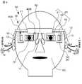
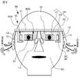
実施例1は、本開示の第1の態様に係る表示装置に関する。実施例1の表示装置を正面から眺めた模式図を図1Aに示し、実施例1の表示装置を側面から眺めた模式図(但し、遮光部材やパッド部等の図示は省略)を図1Bに示し、実施例1の表示装置を上方から眺めた模式図を図2に示す。また、実施例1の表示装置に備えられた遮光部材の効果を説明するための模式図を図3Aに示し、従来の表示装置における問題点を説明するための模式図を図3Bに示し、実施例1の表示装置に備えられた導光板と遮光部材の位置関係を説明するために、これらを上方から眺めたときの模式的な断面図を図3Cに示す。 Example 1 relates to the display device according to the first aspect of the present disclosure. FIG. 1A is a schematic diagram of the display device of Example 1 as viewed from the front, and FIG. 1B is a schematic diagram of the display device of Example 1 as viewed from the side (however, illustration of light shielding members, pads, etc. is omitted). FIG. 2 shows a schematic view of the display device of Example 1 as viewed from above. Further, FIG. 3A shows a schematic diagram for explaining the effect of the light shielding member provided in the display device of Example 1, and FIG. 3B shows a schematic diagram for explaining problems in the conventional display device. In order to explain the positional relationship between the light guide plate and the light shielding member provided in the display device of Example 1, FIG.
実施例1の表示装置1Aあるいは後述する実施例2の表示装置1Bは、具体的には、頭部装着型ディスプレイ(HMD)に用いられる表示装置であり、
観察者50の正面に配置されるフロント部11、フロント部11の両端から延びるテンプル部12、及び、パッド部17を備え、観察者50の頭部に装着されるフレーム10、並びに、
フレーム10に取り付けられた画像表示装置20、
を備えており、
画像表示装置20は、
画像形成装置30、及び、
画像形成装置30から出射された光が入射され、観察者50に向かって出射する光学装置40、
を備えており、
光学装置40の一端部40Aは、フロント部11のテンプル部側に固定されている。Specifically, the
A
an
and
The
an
an
and
One
そして、実施例1の表示装置1Aにおいて、光学装置40の他端部40Bは、フロント部11のパッド部側に配置されており、光学装置40の他端部40Bの上方から光学装置40の他端部40Bへの外光の入射を防ぐ遮光部材60が、フロント部11のパッド部側に取り付けられている。また、図3Cに示すように、光学装置40(具体的には、導光板41)の他端部40Bは、観察者50と対向する遮光部材60の対向面60Aの上を自在に滑動する。場合によっては、光学装置40(具体的には、導光板41)の他端部40Bは、遮光部材60の対向面60Aと離れて、即ち、接触しないように、位置する。 In the
更には、実施例1及び実施例2の表示装置1A,1Bにおいて、光学装置40(具体的には、導光板41)の一端部40Aは、フロント部11のテンプル部側に配設された画像形成装置30に取り付けられている。具体的には、光学装置40の一端部40Aは、例えば、画像形成装置30に接着剤を用いて取り付けられている。 Furthermore, in the
光学装置40は半透過型(シースルー型)である。具体的には、少なくとも観察者50の眼球(瞳)51に対向する光学装置40の部分を半透過(シースルー)とし、光学装置40のこの部分(後述する調光装置が配されている場合には、更に、調光装置)を通して外景を眺めることができる。表示装置1A,1Bは、図示するように画像表示装置20を2つ備えていてもよいし(両眼型)、1つ備えていてもよい(片眼型)。画像形成装置30は、単色(例えば、青色)の画像(虚像)を表示する。 The
ここで、画像形成装置及び光学装置の配置を模式的に示す図8を参照して説明すると、実施例1及び実施例2の表示装置1A,1Bにおいて、光学装置40は、
画像形成装置30から入射された光が内部を全反射により伝播した後、観察者50に向けて出射される導光板41、
導光板41に入射された光が導光板41の内部で全反射されるように、導光板41に入射された光を偏向させる第1偏向手段42、及び、
導光板41の内部を全反射により伝播した光を導光板41から出射させるために、導光板41の内部を全反射により伝播した光を偏向させる第2偏向手段43、
を備えている。即ち、画像形成装置30から入射された光は、導光板41の内部を全反射により伝播した後、観察者50に向けて出射される。導光板41は、全体として画像形成装置30よりも観察者50の顔の中心側に配置されている。8 schematically showing the arrangement of the image forming apparatus and the optical device.
a
a
second deflection means 43 for deflecting the light propagated inside the
It has That is, the light incident from the
光学ガラスやプラスチック材料から成る導光板41は、導光板41の内部全反射による光伝播方向(X方向)と平行に延びる2つの平行面(第1面41A及び第2面41B)を有している。第1面41Aと第2面41Bとは対向している。そして、光入射面に相当する第2面41Bから平行光が入射され、内部を全反射により伝播した後、光出射面に相当する第2面41Bから出射される。但し、これに限定するものではなく、第1面41Aによって光入射面が構成され、第2面41Bによって光出射面が構成されていてもよい。 The
更には、実施例1及び実施例2の表示装置1A,1Bにおいて、画像形成装置30は、フロント部11のテンプル部側に取り付けられている。具体的には、画像形成装置30を内部に格納した筐体30’が、フロント部11に取り付けられている。尚、筐体30’を、テンプル部12に取り付けてもよいし、フロント部11からテンプル部12に亙り取り付けてもよい。画像形成装置30の取付け(筐体30’の取付け)は、例えば、ビスを用いる方法等、適切な方法によって行えばよい。 Furthermore, in the
遮光部材60は、不透明な種々のプラスチック材料や金属材料、合金材料から作製すればよいし、フロント部11のパッド部側への遮光部材60の取付けは、接着剤を用いる方法、ビスを用いる方法等、適切な方法を採用すればよい。遮光部材60は、具体的には、パッド部側のフロント部11の部分に取り付けてもよいし、パッド部17に取り付けてもよい。あるいは又、遮光部材60がフロント部11と一体となった構造とすることもできるし、遮光部材60がパッド部17と一体となった構造とすることもできる。図示した例では、遮光部材60がパッド部17と一体となった構造を有し、遮光部材60が一体となったパッド部17は、フロント部11に取り付けられている。導光板41の上方に位置する遮光部材60の部分の長さは、導光板41の軸線の長さの10%乃至100%、好ましくは、45%乃至65%とすることが好ましく、具体的には、57%を例示することができる。 The
実施例1及び実施例2の表示装置1A,1Bにおいて、2つのテンプル部12のそれぞれは、フロント部11と一体となっている。尚、テンプル部12は、蝶番を介してフロント部11の端部に回動自在に取り付けられていてもよい。即ち、フレーム10は、観察者50の正面に配置されるフロント部11と、フロント部11の両端から延びる2つのテンプル部12と、各テンプル部12の先端部に取り付けられたモダン部(先セル、耳あて、イヤーパッドとも呼ばれる)13から成る。実施例1及び実施例2の表示装置1A,1Bの全体を眺めたとき、フレーム10は、概ね通常の眼鏡やサングラスと略同じ外観である。パッド部17や遮光部材60、フレーム10を構成する材料は、金属や合金、プラスチック、これらの組合せといった、通常の眼鏡やサングラスを構成する材料と同じ材料から構成することができる。 In the
更には、画像形成装置30から延びる配線(信号線や電源線等)14が、テンプル部12、及び、モダン部13の内部を介して、モダン部13の先端部から外部に延び、制御装置(制御回路、制御手段)16に接続されている。更には、画像形成装置30はヘッドホン部15を備えており、画像形成装置30から延びるヘッドホン部用配線15’が、テンプル部12、及び、モダン部13の内部を介して、モダン部13の先端部からヘッドホン部15へと延びている。ヘッドホン部用配線15’は、より具体的には、モダン部13の先端部から、耳介(耳殻)の後ろ側を回り込むようにしてヘッドホン部15へと延びている。このような構成にすることで、ヘッドホン部15やヘッドホン部用配線15’が乱雑に配置されているといった印象を与えることがなく、すっきりとした表示装置とすることができる。 Furthermore, the wiring (signal line, power line, etc.) 14 extending from the
配線(信号線や電源線等)14は、上述したとおり、制御装置(制御回路)16に接続されている。制御装置16には、例えば、画像情報記憶装置(図示せず)が備えられている。そして、制御装置16において画像表示のための処理がなされる。制御装置16、画像情報記憶装置は周知の回路から構成することができる。 The wiring (signal line, power line, etc.) 14 is connected to the control device (control circuit) 16 as described above. The
実施例1及び実施例2の表示装置1A,1Bにおいて、第1偏向手段(第1回折格子部材)42及び第2偏向手段(第2回折格子部材)43は、ホログラム回折格子膜から構成されている。そして、第1偏向手段42は、導光板41に入射された光を回折反射し、第2偏向手段43は、導光板41の内部を全反射により伝播した光を回折反射する。ホログラム回折格子膜は、例えば、反射型のホログラム回折格子膜、具体的には、反射型の体積ホログラム回折格子膜から成る。導光板41は、ガラスや樹脂から構成された透明基板から成る。導光板41の第2面41Bによって入射面が構成され、第2面41Bに対向する導光板41の第1面41Aの上に第1偏向手段(第1回折格子部材)42及び第2偏向手段(第2回折格子部材)43が配設されている。 In the
画像表示装置20については、実施例3~実施例6において詳しく説明する。 The
実施例1の表示装置にあっては、光学装置の他端部の上方から光学装置の他端部に太陽光が入射しないように、遮光部材がフロント部のパッド部側に取り付けられている。それ故、観察者の頭上に太陽が位置し、太陽光が、直接、光学装置を照射した場合であっても、太陽光が光学装置の他端部の端面に入射することが無い。この状態を、図3Aに模式的に図示する。従って、光学装置の内部で迷光が発生して画像の品質低下を招くといった問題の発生を防止することができる。尚、光学装置に遮光部材を備えていない従来の表示装置において、観察者の頭上に太陽が位置し、太陽光が、直接、光学装置を照射した場合、光学装置の他端部の上方から光学装置の他端部の端面に太陽光が入射し、迷光が発生する。この状態を、図3Bに模式的に図示する。また、パッド部に光学装置の質量が加わらないので、あるいは又、加わっても僅かであるので、観察者の鼻が痛くなることがなく、観察者の表示装置装着感に優れている。 In the display device of Example 1, the light shielding member is attached to the pad portion side of the front portion so that sunlight does not enter the other end portion of the optical device from above the other end portion of the optical device. Therefore, even if the sun is positioned above the observer's head and the sunlight directly irradiates the optical device, the sunlight does not enter the end surface of the other end portion of the optical device. This state is schematically illustrated in FIG. 3A. Therefore, it is possible to prevent the occurrence of the problem that stray light is generated inside the optical device and causes deterioration in image quality. In addition, in a conventional display device in which the optical device is not provided with a light shielding member, when the sun is positioned above the observer's head and the sunlight directly irradiates the optical device, the optical device is illuminated from above the other end of the optical device. Sunlight is incident on the end surface of the other end of the device, and stray light is generated. This state is schematically illustrated in FIG. 3B. In addition, since the mass of the optical device is not applied to the pad portion, or even if it is applied only slightly, the viewer's nose does not hurt, and the viewer's feeling of wearing the display device is excellent.
実施例1の表示装置の変形例を正面から眺めた模式図を図4に示すように、遮光部材60を、パッド部側のフロント部11の部分に取り付け、パッド部17もフロント部11に取り付ける構成とすることもできる。 As shown in FIG. 4 which is a schematic diagram of a modification of the display device of the first embodiment viewed from the front, the
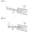
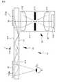
実施例2は、本開示の第2の態様に係る表示装置に関する。実施例2の表示装置を正面から眺めた模式図を図5に示し、観察者が実施例2の表示装置を頭部に装着したときの実施例2の表示装置を上方から眺めた図を図6A及び図6Cに示し、実施例2の表示装置に備えられた導光板と光学装置受け部材の位置関係を説明するために、これらを上方から眺めたときの模式的な断面図を図6B及び図6Dに示す。また、従来の表示装置に備えられた導光板とリムの位置関係を説明するために、これらを上方から眺めたときの模式的な断面図を図7A及び図7Bに示す。 Example 2 relates to the display device according to the second aspect of the present disclosure. FIG. 5 shows a schematic diagram of the display device of Example 2 viewed from the front, and a diagram of the display device of Example 2 viewed from above when an observer wears the display device of Example 2 on the head. In order to explain the positional relationship between the light guide plate and the optical device receiving member, which are shown in FIGS. Shown in FIG. 6D. In order to explain the positional relationship between the light guide plate and the rim provided in the conventional display device, schematic cross-sectional views of these when viewed from above are shown in FIGS. 7A and 7B.
実施例2の表示装置1Bにおいて、光学装置40の他端部40Bは、フロント部11のパッド部側に配置され、フロント部11において自在に滑動する。具体的には、フロント部11のパッド部側には、光学装置受け部材70が取り付けられており、光学装置40の他端部40Bは、光学装置受け部材70の上を自在に滑動する。ここで、
光学装置受け部材70は、仮想水平面で切断したときの断面形状がL字の部材から成り(図6B、図6D参照)、
L字の縦棒の部分に相当する光学装置受け部材70の第1の部分72は、観察者50と対向して垂直方向に延びており、
観察者50から遠い方の光学装置受け部材70の第1の部分72の端部72’から延びるL字の横棒の部分に相当する光学装置受け部材70の第2の部分73は、フロント部11のテンプル部側に向かって延びており、
光学装置40の他端部40Bは、光学装置受け部材70の第2の部分の観察者50と対向する対向面71の上を自在に滑動する。In the
The optical
A
The
The
光学装置受け部材70は、不透明な種々のプラスチック材料や金属材料、合金材料から作製すればよいし、フロント部11のパッド部側への光学装置受け部材70の取付けは、接着剤を用いる方法、ビスを用いる方法等、適切な方法を採用すればよい。光学装置受け部材70は、具体的には、パッド部側のフロント部11の部分に取り付けてもよいし、パッド部17に取り付けてもよいし、光学装置受け部材70がフロント部11と一体となった構造とすることもできるし、光学装置受け部材70がパッド部と一体となった構造とすることもできる。図示した例では、光学装置受け部材70は、パッド部側のフロント部11の部分に取り付けている。パッド部17はフロント部11に取り付けられている。導光板41に対向する光学装置受け部材70の部分の長さは、導光板41の幅方向の長さの
20%乃至100%とすることが好ましく、具体的には、70%を例示することができる。The optical
前述したように、表示装置1Bの設計条件と同じあるいは条件に近い観察者50が、表示装置1Bを頭部に装着したときの状態を、表示装置1Bを上方から眺めた図として図6Aに示す。尚、図6A及び図6Cにおいて、光学装置受け部材70及びパッド部17の図示は省略した。一方、この表示装置1Bを、表示装置1Bの設計条件よりも大きな観察者50が頭部に装着したときの状態を、表示装置1Bを上方から眺めた図として図6Cに示す。そして、この場合、図6Cに示すように、テンプル部12が外側に広がってしまう。尚、図6Cにおいて、表示装置1Bの設計条件と同じあるいは条件に近い観察者50が、表示装置1Bを頭部に装着したときの状態を、点線で示す。その結果、このような場合、フレーム10の正面部に応力が加わり、テンプル部12とパッド部17との間のフレーム10の正面部の領域が歪んでしまう。 As described above, FIG. 6A shows a state in which the
従来の表示装置においては、図7A及び図7Bに示すように、導光板41の端部は、リム170の凹部内に納められている。テンプル部12が外側に広がると、導光板41は、図7Bの点線で示す状態から実線で示す状態へと位置変化が生じる。その結果、導光板41の端部は、リム170の凹部と強く接触し、導光板41にも応力が加わり、導光板41に変形が生じ、観察者が観察する画像にも歪みが発生する。 In the conventional display device, as shown in FIGS. 7A and 7B, the end portion of the
一方、上述したとおり、実施例2の表示装置1Bにあっては、光学装置40の他端部40Bは、フロント部11のパッド部側に配置され、フロント部11において自在に滑動する。従って、テンプル部12が外側に広がると、導光板41は、図6Bの実線(図6Dの点線)で示す状態から図6Dの実線で示す状態へと位置変化が生じるが、導光板41の端部は光学装置受け部材70の上を自在に滑動するので、導光板41に応力が加わることが無く、導光板41に変形が生じることが無い。それ故、観察者が観察する画像に歪みが発生することも無い。尚、光学装置40(具体的には、導光板41)の他端部40Bは、その位置によっては、光学装置受け部材70の対向面71と離れた状態、即ち、接触していない状態となる場合もある。 On the other hand, as described above, in the
以上のとおり、実施例2の表示装置にあっては、光学装置の他端部は、フロント部のパッド部側に配置され、フロント部において自在に滑動するので、観察者が表示装置を頭部に装着したときテンプル部が外側に広がった場合であっても光学装置に歪みが生じ難く、観察者が観察する画像の画質への影響が少ない。また、パッド部に光学装置の質量が加わらないので、あるいは又、加わっても僅かであるので、観察者の鼻が痛くなることがなく、観察者の表示装置装着感に優れている。 As described above, in the display device of Example 2, the other end portion of the optical device is arranged on the pad portion side of the front portion and freely slides on the front portion, so that the observer can hold the display device on the head. Even if the temple portion expands outward when the optical device is worn, the optical device is less likely to be distorted, and the quality of the image observed by the observer is less affected. In addition, since the mass of the optical device is not applied to the pad portion, or even if it is applied only slightly, the viewer's nose does not hurt, and the viewer's feeling of wearing the display device is excellent.
以上の点を除き、実施例2の表示装置の構成、構造は、実施例1において説明した表示装置の構成、構造と同様とすることができるので、詳細な説明は省略する。 Except for the above points, the configuration and structure of the display device of Example 2 can be the same as the configuration and structure of the display device described in Example 1, so detailed description thereof will be omitted.
実施例3~実施例5においては、画像形成装置及び光学装置の説明を行う。実施例3にあっては、実施例1において説明した表示装置を構成する画像形成装置及び光学装置の説明を行うが、これらの画像形成装置及び光学装置の配置を模式的に図8に示す。 In Examples 3 to 5, an image forming apparatus and an optical device will be described. In Example 3, an image forming apparatus and an optical device that constitute the display device described in Example 1 will be described, and the arrangement of these image forming device and optical device is schematically shown in FIG.
実施例3の表示装置において、第1偏向手段42及び第2偏向手段43は、具体的には、導光板41の表面(具体的には、導光板41の第1面41A)に配設されている(具体的には、貼り合わされている)。そして、第1偏向手段42は、導光板41に入射された光を回折反射し、第2偏向手段43は、導光板41の内部を全反射により伝播した光を回折反射する。第1偏向手段42及び第2偏向手段43は、前述したとおり、回折格子部材、具体的には反射型回折格子部材、より具体的には反射型体積ホログラム回折格子部材から成る。以下の説明において、ホログラム回折格子部材から成る第1偏向手段を、便宜上、『第1回折格子部材42』と呼び、ホログラム回折格子部材から成る第2偏向手段を、便宜上、『第2回折格子部材43』と呼ぶ。 In the display device of Example 3, specifically, the
そして、実施例3あるいは後述する実施例4において、第1回折格子部材42及び第2回折格子部材43は、1層の回折格子層から成る構成とされている。フォトポリマー材料から成る各回折格子層には、1種類の波長帯域(あるいは、波長)に対応する干渉縞が形成されており、従来の方法で作製されている。回折格子層(回折光学素子)に形成された干渉縞のピッチは一定であり、干渉縞は直線状であり、Y方向に平行である。第1回折格子部材42及び第2回折格子部材43の軸線はX方向と平行であり、法線はZ方向と平行である。 In Example 3 or Example 4, which will be described later, the first
図9Aに反射型体積ホログラム回折格子部材の拡大した模式的な一部断面図を示す。反射型体積ホログラム回折格子部材には、傾斜角(スラント角)φを有する干渉縞が形成されている。傾斜角φとは、反射型体積ホログラム回折格子部材の表面と干渉縞の成す角度を指す。干渉縞は、反射型体積ホログラム回折格子部材の内部から表面に亙り、形成されている。干渉縞は、ブラッグ条件を満たしている。ブラッグ条件とは、以下の式(A)を満足する条件を指す。式(A)中、mは正の整数、λは波長、dは格子面のピッチ(干渉縞を含む仮想平面の法線方向の間隔)、Θは干渉縞へ入射する角度の余角を意味する。また、入射角ψにて回折格子部材に光が侵入した場合の、Θ、傾斜角φ、入射角ψの関係は、式(B)のとおりである。 FIG. 9A shows an enlarged schematic partial cross-sectional view of the reflective volume hologram diffraction grating member. An interference fringe having an inclination angle (slant angle) φ is formed in the reflection type volume hologram diffraction grating member. The tilt angle φ refers to the angle formed between the surface of the reflective volume hologram diffraction grating member and the interference fringes. Interference fringes are formed from the inside to the surface of the reflective volume hologram diffraction grating member. The interference fringes satisfy the Bragg condition. The Bragg condition refers to a condition that satisfies the following formula (A). In formula (A), m is a positive integer, λ is the wavelength, d is the grating plane pitch (distance in the normal direction of the virtual plane containing the interference fringes), and Θ is the complementary angle of the incident angle to the interference fringes. do. Also, the relationship between Θ, the tilt angle φ, and the incident angle ψ when light enters the diffraction grating member at the incident angle ψ is as shown in formula (B).
m・λ=2・d・sin(Θ) (A)
Θ=90°-(φ+ψ) (B)m·λ=2·d·sin(Θ) (A)
Θ=90°-(φ+ψ) (B)
第1回折格子部材42は、上述したとおり、導光板41の第1面41Aに配設(接着)されており、第2面41Bから導光板41に入射されたこの平行光が導光板41の内部で全反射されるように、導光板41に入射されたこの平行光を回折反射する。更には、第2回折格子部材43は、上述したとおり、導光板41の第1面41Aに配設(接着)されており、導光板41の内部を全反射により伝播したこの平行光を回折反射し、導光板41から平行光のまま第2面41Bから出射する。 As described above, the first
そして、導光板41において、平行光が内部を全反射により伝播した後、出射される。このとき、導光板41が薄く導光板41の内部を進行する光路が長いため、各画角によって第2回折格子部材43に至るまでの全反射回数は異なっている。より詳細に述べれば、導光板41に入射する平行光のうち、第2回折格子部材43に近づく方向の角度をもって入射する平行光の反射回数は、第2回折格子部材43から離れる方向の角度をもって導光板41に入射する平行光の反射回数よりも少ない。これは、第1回折格子部材42において回折反射される平行光であって、第2回折格子部材43に近づく方向の角度をもって導光板41に入射する平行光の方が、これと逆方向の角度をもって導光板41に入射する平行光よりも、導光板41の内部を伝播していく光が導光板41の内面と衝突するときの導光板41の法線と成す角度が小さくなるからである。また、第2回折格子部材43の内部に形成された干渉縞の形状と、第1回折格子部材42の内部に形成された干渉縞の形状とは、導光板41の軸線に垂直な仮想平面に対して対称な関係にある。第1回折格子部材42及び第2回折格子部材43の導光板41とは対向していない面を、透明樹脂板あるいは透明樹脂フィルムで被覆し、第1回折格子部材42及び第2回折格子部材43に損傷が生じることを防止する構造としてもよい。また、第2面41Bに透明な保護フィルムを貼り合わせ、導光板41を保護してもよい。 Then, in the
後述する実施例4における導光板41も、基本的には、以上に説明した導光板41の構成、構造と同じ構成、構造を有する。 A
実施例3あるいは後述する実施例5において、画像形成装置30は、第1構成の画像形成装置であり、2次元マトリクス状に配列された複数の画素を有する。具体的には、画像形成装置30は、有機EL表示装置31Bを備えている。有機EL表示装置31Bから出射され画像は、レンズ系を構成する第1の凸レンズ31Cを通過し、更に、レンズ系を構成する第2の凸レンズ31Eを通過し、平行光となって、導光板41へと向かう。第1の凸レンズ31Cの後方焦点f1Bに、第2の凸レンズ31Eの前方焦点f2Fが位置する。また、第1の凸レンズ31Cの後方焦点f1B(第2の凸レンズ31Eの前方焦点f2F)の位置に、絞り31Dが配置されている。絞り31Dは画像出射部に該当する。画像形成装置30の全体は、筐体31A(筐体30’)内に納められている。筐体31Aは、適切な手段でフレーム10に取り付けられている。有機EL表示装置31Bは、2次元マトリクス状に配列された複数(例えば、640×480個)の画素(有機EL素子)を備えている。In Example 3 or Example 5, which will be described later, the
あるいは又、図9Bに示すように、画像形成装置30は、第1構成の画像形成装置であり、2次元マトリクス状に配列された複数の画素を有する。具体的には、画像形成装置30は、反射型空間光変調装置、及び、白色光を出射する発光ダイオードから成る光源32Bから構成されている。画像形成装置30全体は、筐体32A(図9Bでは、一点鎖線で示す)内に納められており、係る筐体32A(筐体30’)には開口部(図示せず)が設けられており、開口部を介して光学系(平行光出射光学系、コリメート光学系32E)から光が出射される。筐体32Aは、適切な手段でフレーム10に取り付けられている。反射型空間光変調装置は、ライト・バルブとしてのLCOSから成る液晶表示装置(LCD)32Dから成る。更には、光源32Bからの光の一部を反射して液晶表示装置32Dへと導き、且つ、液晶表示装置32Dによって反射された光の一部を通過させて光学系32Eへと導く偏光ビームスプリッター32Cが備えられている。液晶表示装置32Dは、2次元マトリクス状に配列された複数(例えば、640×480個)の画素(液晶セル、液晶表示素子)を備えている。偏光ビームスプリッター32Cは、周知の構成、構造を有する。光源32Bから出射された無偏光の光は、偏光ビームスプリッター32Cに衝突する。偏光ビームスプリッター32Cにおいて、P偏光成分は通過し、系外に出射される。一方、S偏光成分は、偏光ビームスプリッター32Cにおいて反射され、液晶表示装置32Dに入射し、液晶表示装置32Dの内部で反射され、液晶表示装置32Dから出射される。ここで、液晶表示装置32Dから出射した光の内、「白」を表示する画素から出射した光にはP偏光成分が多く含まれ、「黒」を表示する画素から出射した光にはS偏光成分が多く含まれる。従って、液晶表示装置32Dから出射され、偏光ビームスプリッター32Cに衝突する光の内、P偏光成分は、偏光ビームスプリッター32Cを通過し、光学系32Eへと導かれる。一方、S偏光成分は、偏光ビームスプリッター32Cにおいて反射され、光源32Bに戻される。光学系32Eは、例えば凸レンズから構成され、平行光を生成させるために、光学系32Eにおける焦点距離の所(位置)に画像形成装置30(より具体的には、液晶表示装置32D)が配置されている。画像形成装置30から出射された画像は、光学装置40を介して観察者50の瞳51に到達する。 Alternatively, as shown in FIG. 9B, the
画像表示装置20において表示する画像に関する情報やデータ、あるいは又、受信装置が受け取るべき信号は、例えば、所謂クラウドコンピュータやサーバーに記録、保管、保存されており、表示装置1A,1Bが通信手段(送受信装置)、例えば、携帯電話機やスマートフォンを備えることによって、あるいは又、表示装置1A,1Bに備えられた制御装置(制御回路、制御手段)16に通信手段(受信装置)を組み込むことで、通信手段を介してクラウドコンピュータやサーバーと表示装置1A,1Bとの間での各種情報やデータ、信号の授受、交換を行うことができるし、各種情報やデータに基づく信号、即ち、画像表示装置20において画像を表示するための信号を受け取ることができるし、受信装置は信号を受け取ることができる。 Information and data related to images displayed on the
具体的には、観察者が、携帯電話機やスマートフォンに、入手すべき「情報」を要求する旨の入力を行うと、携帯電話機やスマートフォンは、クラウドコンピュータやサーバーにアクセスし、「情報」をクラウドコンピュータやサーバーから入手する。こうして、制御装置16は、画像表示装置20において画像を表示するための信号を受け取る。制御装置16にあっては、この信号に基づいて周知の画像処理を行い、画像形成装置30に「情報」を画像として表示する。この「情報」を画像は、導光板41において、画像形成装置30から出射される光に基づき、制御装置16によって制御された所定の位置に虚像として表示される。即ち、虚像形成領域(第2偏向手段43)の一部分において虚像が形成される。 Specifically, when an observer inputs a request for "information" to be obtained to a mobile phone or smartphone, the mobile phone or smartphone accesses a cloud computer or server and sends "information" to the cloud. Get it from your computer or server. Thus,
場合によっては、画像表示装置20において画像を表示するための信号が、表示装置1A,1B(具体的には、制御装置16)に記憶されていてもよい。 In some cases, signals for displaying images on
あるいは又、表示装置1A,1Bに備えられたカメラ(図示せず)によって撮像された画像を通信手段を介してクラウドコンピュータやサーバーに送出し、クラウドコンピュータやサーバーにおいてカメラによって撮像された画像に該当する各種情報やデータを検索し、検索された各種情報やデータを通信手段を介して表示装置1A,1Bに送出し、検索された各種情報やデータを画像表示装置20において画像を表示してもよい。また、このような形態と「情報」の入力を併用すれば、例えば、観察者のいる場所等や観察者がどの方向を向いているか等の情報を加重することができるので、一層高い精度で、「情報」を画像形成装置30において表示することができる。 Alternatively, an image captured by a camera (not shown) provided in the
実施例4の表示装置(頭部装着型ディスプレイ)における画像表示装置20の概念図を図10に示すように、実施例4において、画像形成装置30は、第2構成の画像形成装置から構成されている。即ち、光源33B、光源33Bから出射された平行光を2次元的に走査する走査手段33C、及び、光源33Bから出射された光を平行光とするレンズ系33Dから構成されている。画像形成装置30全体が筐体33A(筐体30’)内に納められており、係る筐体33Aには開口部(図示せず)が設けられており、開口部を介してレンズ系33Dから光が出射される。そして、筐体33Aは、適切な手段でフレーム10に取り付けられている。 As shown in FIG. 10, which is a conceptual diagram of the
光源33Bは、例えば、半導体レーザ素子から構成されている。そして、光源33Bから出射された光は、図示しないレンズによって平行光とされ、マイクロミラーを二次元方向に回転自在とし、入射した平行光を2次元的に走査することができるMEMSミラーから成る走査手段33Cによって水平走査及び垂直走査が行われ、一種の2次元画像化され、仮想の画素(画素数は、例えば、実施例3と同じとすることができる)が生成される。そして、そして、仮想の画素(画像出射部に該当する走査手段33C)からの光は、正の光学的パワーを持つレンズ系33Dを通過し、平行光とされた光束が導光板41に入射する。 The
実施例5の表示装置(頭部装着型ディスプレイ)における画像表示装置20の概念図を図11に示すように、実施例5において、第1偏向手段42’及び第2偏向手段43’は導光板41’の内部に配設されている。そして、第1偏向手段42’は、導光板41’に入射された光を反射し、第2偏向手段43’は、導光板41’の内部を全反射により伝播した光を、複数回に亙り、透過、反射する。即ち、第1偏向手段42’は反射鏡として機能し、第2偏向手段43’は半透過鏡として機能する。より具体的には、導光板41’の内部に設けられた第1偏向手段42’は、アルミニウム(Al)から成り、導光板41’に入射された光を反射させる光反射膜(一種のミラー)から構成されている。一方、導光板41’の内部に設けられた第2偏向手段43’は、誘電体積層膜が多数積層された多層積層構造体から構成されている。誘電体積層膜は、例えば、高誘電率材料としてのTiO2膜、及び、低誘電率材料としてのSiO2膜から構成されている。誘電体積層膜が多数積層された多層積層構造体に関しては、特表2005-521099に開示されている。図面においては6層の誘電体積層膜を図示しているが、これに限定するものではない。誘電体積層膜と誘電体積層膜との間には、導光板41’を構成する材料と同じ材料から成る薄片が挟まれている。第1偏向手段42’においては、導光板41’に入射された平行光が導光板41’の内部で全反射されるように、導光板41’に入射された平行光が反射される。一方、第2偏向手段43’においては、導光板41’の内部を全反射により伝播した平行光が複数回に亙り反射され、導光板41’から平行光の状態で、観察者50の瞳51に向かって出射される。As shown in FIG. 11, which is a conceptual diagram of an
第1偏向手段42’は、導光板41’の第1偏向手段42’を設ける部分44を切り出すことで、導光板41’に第1偏向手段42’を形成すべき斜面を設け、係る斜面に光反射膜を真空蒸着した後、導光板41’の切り出した部分44を第1偏向手段42’に接着すればよい。また、第2偏向手段43’は、導光板41’を構成する材料と同じ材料(例えば、ガラス)と誘電体積層膜(例えば、真空蒸着法にて成膜することができる)とが多数積層された多層積層構造体を作製し、導光板41’の第2偏向手段43’を設ける部分45を切り出して斜面を形成し、係る斜面に多層積層構造体を接着し、研磨等を行って、外形を整えればよい。こうして、導光板41’の内部に第1偏向手段42’及び第2偏向手段43’が設けられた光学装置40を得ることができる。 The first deflecting means 42' is formed by cutting out a
あるいは又、実施例5の表示装置(頭部装着型ディスプレイ)の変形例における画像表示装置20の概念図を図12に示す。図12に示す例では、画像形成装置30は、実施例4と同様に、第2構成の画像形成装置から構成されている。 Alternatively, FIG. 12 shows a conceptual diagram of an
実施例6は、実施例1~実施例5の変形であり、光学装置40は、更に、外部から入射する外光の光量を調整する調光装置を備えている Example 6 is a modification of Examples 1 to 5, and the
詳細は後述するが、調光装置は、
第1基板、
第1基板と対向する第2基板、
第2基板と対向する第1基板の対向面に設けられた第1透明電極、
第1基板と対向する第2基板の対向面に設けられた第2透明電極、及び、
第1透明電極と第2透明電極とによって挟まれた調光層、
から成る形態とすることができる。そして、この場合、例えば、
第1透明電極は、第1の方向に延びる複数の帯状の第1透明電極セグメントから構成されており、
第2透明電極は、第1の方向とは異なる第2の方向に延びる複数の帯状の第2透明電極セグメントから構成されており、
第1透明電極セグメントと第2透明電極セグメントの重複領域(調光装置の遮光率が変化する最小単位領域)に対応する調光装置の部分の遮光率の制御は、第1透明電極セグメント及び第2透明電極セグメントに印加する電圧の制御に基づき行われる形態とすることができる。即ち、遮光率の制御を単純マトリクス方式に基づき行うことができる。第1の方向と第2の方向とは直交している形態を例示することができる。調光装置の動作時、調光装置の動作時、例えば、第1透明電極には第2透明電極よりも高い電圧が印加される。Although the details will be described later, the light control device
a first substrate,
a second substrate facing the first substrate;
a first transparent electrode provided on the facing surface of the first substrate facing the second substrate;
a second transparent electrode provided on the facing surface of the second substrate facing the first substrate; and
a light control layer sandwiched between the first transparent electrode and the second transparent electrode;
It can be in the form of And in this case, for example,
The first transparent electrode is composed of a plurality of strip-shaped first transparent electrode segments extending in a first direction,
The second transparent electrode is composed of a plurality of strip-shaped second transparent electrode segments extending in a second direction different from the first direction,
Control of the light blocking rate of the portion of the light control device corresponding to the overlapping region of the first transparent electrode segment and the second transparent electrode segment (minimum unit region where the light blocking rate of the light control device changes) is performed by the first transparent electrode segment and the second transparent electrode segment. It is also possible to adopt a mode in which it is performed based on the control of the voltage applied to the two transparent electrode segments. That is, the control of the light shielding rate can be performed based on the simple matrix method. A form in which the first direction and the second direction are orthogonal can be exemplified. During operation of the light control device, for example, a higher voltage is applied to the first transparent electrode than to the second transparent electrode.
あるいは又、調光装置の遮光率が変化する最小単位領域の遮光率の制御のために、最小単位領域のそれぞれに薄膜トランジスタ(TFT)を設けてもよい。即ち、遮光率の制御をアクティブマトリクス方式に基づき行ってもよい。あるいは又、第1透明電極及び第2透明電極の少なくとも一方を所謂ベタ電極(パターニングされていない電極)とすることもできる。 Alternatively, a thin film transistor (TFT) may be provided in each of the minimum unit areas in order to control the light shielding rate of the minimum unit area where the light shielding rate of the dimmer changes. That is, the light shielding rate may be controlled based on the active matrix method. Alternatively, at least one of the first transparent electrode and the second transparent electrode can be a so-called solid electrode (non-patterned electrode).
第1基板及び第2基板の内のいずれか一方の基板が導光板を兼ねている構成とすることができ、このような構成とすることで、表示装置全体の重量の減少を図ることができ、表示装置の使用者に不快感を感じさせる虞が無い。第1基板及び第2基板の内のいずれか一方の基板は他方の基板よりも薄い構成とすることができる。調光装置を備えた表示装置にあっては、画像形成装置において画像を表示するための信号に基づき、調光装置の実際に調光する領域の大きさ及び位置を決定すればよい。調光装置の大きさは、光学装置と同じ大きさでもよいし、大きくてもよいし、小さくともよい。要は、調光装置の正射影像内に第2偏向手段(虚像形成領域)が位置していればよい。 Either one of the first substrate and the second substrate may also serve as a light guide plate. With such a configuration, the weight of the entire display device can be reduced. , there is no fear of making the user of the display device feel uncomfortable. Either one of the first substrate and the second substrate may be thinner than the other substrate. In a display device provided with a light control device, the size and position of an area to be actually controlled by the light control device may be determined based on a signal for displaying an image in the image forming device. The size of the light control device may be the same size as the optical device, may be larger, or may be smaller. The point is that the second deflection means (virtual image forming area) should be positioned within the orthogonal projection image of the light control device.
調光層は、無機又は有機のエレクトロクロミック材料の酸化還元反応によって発生する物質の色変化を応用した光シャッタから成る形態とすることができる。具体的には、調光層は無機又は有機のエレクトロクロミック材料を含む形態とすることができ、更には、調光層は、第1透明電極側から、WO3層/Ta2O5層/IrXSn1-XO層といった無機エレクトロクロミック材料層の積層構造、あるいは又、WO3層/Ta2O5層/IrOx層といった無機エレクトロクロミック材料層の積層構造を有する形態とすることができる。WO3層の代わりに、MoO3層やV2O5層を用いることができる。また、IrOx層の代わりに、ZrO2層、リン酸ジルコニウム層を用いることができるし、あるいは又、プルシアンブルー錯体/ニッケル置換プルシアンブルー錯体等を用いることもできる。有機のエレクトロクロミック材料として、例えば、特開2014-111710号公報や特開2014-159385号公報に開示されたエレクトロクロミック材料を用いることもできる。また、調光層を、電気泳動分散液から構成することもできるし、調光装置を、金属(例えば、銀粒子)の可逆的な酸化還元反応によって発生する電着・解離現象を応用した電着方式(エレクトロデポジション・電界析出)による光シャッタ、即ち、調光層は金属イオンを含む電解質を含む形態とすることもできる。調光層を金属イオンを含む電解質層から構成する場合、金属イオンは銀イオンから成り、電解質は、LiX、NaX及びKX(但し、Xはフッ素原子、塩素原子、臭素原子又はヨウ素原子である)から成る群より選ばれた少なくとも1種類の塩を含むことが望ましい。あるいは又、調光装置として、場合によっては、液晶シャッタや、エレクトロウェッティング現象によって透過率を制御する光シャッタを用いることもできる。また、調光装置によって着色される色を、黒色等の固定色とすることもできるし、調光装置を通過する光は、調光装置によって所望の色に着色され、しかも、調光装置によって着色される色は可変である形態とすることもできる。具体的には、例えば、赤色に着色される調光装置と、緑色に着色される調光装置と、青色に着色される調光装置とを積層すればよい。The light-modulating layer can be in the form of a light shutter that applies the color change of substances generated by the oxidation-reduction reaction of inorganic or organic electrochromic materials. Specifically, the light-modulating layer can be in the form of containing an inorganic or organic electrochromic material, and further, the light-modulating layer is composed of, from the first transparent electrode side, WO3 layer/Ta2 O5 layer/ A laminated structure of inorganic electrochromic material layers such as anIrxSn1-xO layer, or a laminated structure of inorganic electrochromic material layers such as aWO3 layer/Ta2O5 layer/IrOx layer may be employed. can. Instead of theWO3 layer, aMoO3 layer or aV2O5 layer can be used. Also, instead of theIrOx layer, a ZrO2 layer, a zirconium phosphate layer, or a Prussian blue complex/nickel- substituted Prussian blue complex, etc. may be used. As the organic electrochromic material, for example, the electrochromic materials disclosed in JP-A-2014-111710 and JP-A-2014-159385 can also be used. In addition, the light control layer can be composed of an electrophoretic dispersion liquid, and the light control device can be an electrophoretic layer that applies the electrodeposition/dissociation phenomenon generated by the reversible oxidation-reduction reaction of metal (for example, silver particles). The optical shutter by the deposition method (electrodeposition/electrodeposition), that is, the light control layer can also be in a form containing an electrolyte containing metal ions. When the light control layer is composed of an electrolyte layer containing metal ions, the metal ions are composed of silver ions, and the electrolyte is LiX, NaX and KX (where X is a fluorine atom, a chlorine atom, a bromine atom or an iodine atom). It is desirable to contain at least one salt selected from the group consisting of Alternatively, depending on the circumstances, a liquid crystal shutter or an optical shutter that controls the transmittance by an electrowetting phenomenon can be used as the light control device. Further, the color that is colored by the light control device can be a fixed color such as black, and the light that passes through the light control device can be colored in a desired color by the light control device and It can also be in the form that the color applied is variable. Specifically, for example, a red-colored light control device, a green-colored light control device, and a blue-colored light control device may be stacked.
あるいは又、調光層は電気泳動分散液を含む形態とすることができるし、調光装置を、金属(例えば、銀粒子)の可逆的な酸化還元反応によって発生する電着・解離現象を応用した電着方式(エレクトロデポジション・電界析出)による光シャッタ、即ち、調光層は金属イオンを含む電解質を含む形態とすることもできる。 Alternatively, the light control layer can be in the form of containing an electrophoretic dispersion liquid, and the light control device can be applied to the electrodeposition/dissociation phenomenon generated by the reversible oxidation-reduction reaction of metal (for example, silver particles). The light shutter by the electrodeposition method (electrodeposition/electrodeposition), that is, the light control layer can also be in the form of containing an electrolyte containing metal ions.
ここで、電気泳動分散液は、帯電した多数の電気泳動粒子、及び、電気泳動粒子とは異なる色の分散媒から構成される。例えば、第1透明電極にパターニングを施し、第2透明電極にはパターニングを施さない場合(所謂ベタ電極構成)であって、電気泳動粒子を負に帯電させた場合、第1透明電極に相対的に負の電圧を印加し、第2透明電極に相対的に正の電圧を印加すると、負に帯電している電気泳動粒子は第2透明電極を覆うように泳動する。従って、調光装置における遮光率は高い値となる。一方、これとは逆に、第1透明電極に相対的に正の電圧を印加し、第2透明電極に相対的に負の電圧を印加すると、電気泳動粒子は第1透明電極を覆うように泳動する。従って、調光装置における遮光率は低い値となる。このような透明電極への印加を適切に行うことで、調光装置における遮光率の制御を行うことができる。電圧は直流であってもよいし、交流であってもよい。パターニングされた第1透明電極の形状は、電気泳動粒子が第1透明電極を覆うように泳動し、調光装置における遮光率が低い値となったとき、調光装置における遮光率の値の最適化を図れるような形状とすればよく、種々の試験を行い決定すればよい。必要に応じて、透明電極の上に絶縁層を形成してもよい。係る絶縁層を構成する材料として、例えば、無色透明な絶縁性樹脂を挙げることができ、具体的には、例えば、アクリル系樹脂、エポキシ系樹脂、フッ素系樹脂、シリコーン系樹脂、ポリイミド系樹脂、ポリスチレン系樹脂等を挙げることができる。 Here, the electrophoretic dispersion liquid is composed of a large number of charged electrophoretic particles and a dispersion medium having a color different from that of the electrophoretic particles. For example, when the first transparent electrode is patterned and the second transparent electrode is not patterned (so-called solid electrode configuration), and the electrophoretic particles are negatively charged, relative to the first transparent electrode, When a negative voltage is applied to the second transparent electrode and a relatively positive voltage is applied to the second transparent electrode, the negatively charged electrophoretic particles migrate so as to cover the second transparent electrode. Therefore, the light shielding rate of the light control device becomes a high value. Conversely, when a relatively positive voltage is applied to the first transparent electrode and a relatively negative voltage is applied to the second transparent electrode, the electrophoretic particles cover the first transparent electrode. migrate. Therefore, the light shielding rate of the light control device becomes a low value. By appropriately applying voltage to the transparent electrode, the light shielding rate of the light control device can be controlled. The voltage may be direct current or alternating current. The shape of the patterned first transparent electrode is such that when the electrophoretic particles migrate so as to cover the first transparent electrode and the light shielding ratio in the light control device becomes a low value, the value of the light shielding ratio in the light control device is optimized. It may be determined by conducting various tests. An insulating layer may be formed on the transparent electrode, if necessary. Examples of materials constituting such an insulating layer include colorless and transparent insulating resins, and specific examples include acrylic resins, epoxy resins, fluorine resins, silicone resins, polyimide resins, Polystyrene-based resins and the like can be mentioned.
調光装置を構成する透明な第1基板及び第2基板を構成する材料として、具体的には、ソーダライムガラス、白板ガラス等の透明なガラス基板や、プラスチック基板、プラスチック・シート、プラスチック・フィルムを挙げることができる。ここで、プラスチックとして、ポリエチレンテレフタレート、ポリエチレンナフタレート、ポリカーボネート、酢酸セルロース等のセルロースエステル、ポリフッ化ビニリデンあるいはポリテトラフルオロエチレンとヘキサフルオロプロピレンとの共重合体等のフッ素系ポリマー、ポリオキシメチレン等のポリエーテル、ポリアセタール、ポリスチレン、ポリエチレン、ポリプロピレン、メチルペンテンポリマー等のポリオレフィン、ポリアミドイミドあるいはポリエーテルイミド等のポリイミド、ポリアミド、ポリエーテルサルフォン、ポリフェニレンサルファイド、ポリフッ化ビニリデン、テトラアセチルセルロース、ブロム化フェノキシ、ポリアリレート、ポリスルフォン等を挙げることができる。プラスチック・シート、プラスチック・フィルムは、容易に曲がらない剛性を有していてもよいし、可撓性を有していてもよい。第1基板及び第2基板を透明なプラスチック基板から構成する場合、基板内面に無機材料あるいは有機材料から成るバリア層を形成しておいてもよい。 Specific examples of materials for the transparent first and second substrates of the light control device include transparent glass substrates such as soda lime glass and white plate glass, plastic substrates, plastic sheets, and plastic films. can be mentioned. Examples of plastics include polyethylene terephthalate, polyethylene naphthalate, polycarbonate, cellulose esters such as cellulose acetate, fluorine-based polymers such as polyvinylidene fluoride or copolymers of polytetrafluoroethylene and hexafluoropropylene, and polyoxymethylene. polyether, polyacetal, polystyrene, polyethylene, polypropylene, polyolefin such as methylpentene polymer, polyimide such as polyamideimide or polyetherimide, polyamide, polyether sulfone, polyphenylene sulfide, polyvinylidene fluoride, tetraacetyl cellulose, brominated phenoxy, Polyarylates, polysulfones and the like can be mentioned. The plastic sheet and plastic film may have a rigidity that does not bend easily, or may have flexibility. When the first substrate and the second substrate are made of transparent plastic substrates, a barrier layer made of an inorganic material or an organic material may be formed on the inner surfaces of the substrates.
第1基板と第2基板とは、外縁部において封止部材によって封止され、接着されている。シール剤とも呼ばれる封止部材として、エポキシ系樹脂、ウレタン系樹脂、アクリル系樹脂、酢酸ビニル系樹脂、エン-チオール系樹脂、シリコーン系樹脂、変性ポリマー樹脂等の、熱硬化型、光硬化型、湿気硬化型、嫌気硬化型等の各種樹脂を用いることができる。 The first substrate and the second substrate are sealed and bonded together by a sealing member at their outer edges. As a sealing member, also called a sealant, thermosetting, photo-curing, epoxy resin, urethane resin, acrylic resin, vinyl acetate resin, ene-thiol resin, silicone resin, modified polymer resin, etc. Various resins such as moisture-curable and anaerobic-curable resins can be used.
前述したとおり、第1透明電極は、パターニングされていてもよいし、パターニングされていなくともよい。第2透明電極も、パターニングされていてもよいし、パターニングされていなくともよい。第1透明電極及び第2透明電極を構成する材料として、具体的には、インジウム-スズ複合酸化物(ITO,Indium Tin Oxide,SnドープのIn2O3、結晶性ITO及びアモルファスITOを含む)、フッ素ドープSnO2(FTO)、IFO(FドープのIn2O3)、アンチモンドープSnO2(ATO)、SnO2、ZnO(AlドープのZnOやBドープのZnOを含む)、インジウム-亜鉛複合酸化物(IZO,Indium Zinc Oxide)、スピネル型酸化物、YbFe2O4構造を有する酸化物、ポリアニリン、ポリピロール、ポリチオフェン等の導電性高分子等を挙げることができるが、これらに限定されるものではなく、また、これらを2種類以上組み合わせて用いることもできる。第1透明電極や第2透明電極は、真空蒸着法やスパッタリング法等の物理的気相成長法(PVD法)、各種化学的気相成長法(CVD法)、各種塗布法等に基づき形成することができるし、パターニングは、エッチング法、リフトオフ法、各種マスクを用いる方法等、任意の方法で行うことができる。As described above, the first transparent electrode may or may not be patterned. The second transparent electrode may also be patterned or may not be patterned. Specifically, indium-tin composite oxides (including ITO, Indium Tin Oxide, Sn-doped In2 O3 , crystalline ITO, and amorphous ITO) are used as materials for forming the first transparent electrode and the second transparent electrode. , fluorine-doped SnO2 (FTO), IFO (F-doped In2 O3 ), antimony-doped SnO2 (ATO), SnO2 , ZnO (including Al-doped ZnO and B-doped ZnO), indium-zinc composite Examples include oxides (IZO, Indium Zinc Oxide),spinel -type oxides, oxides having aYbFe2O4 structure, conductive polymers such as polyaniline, polypyrrole, and polythiophene, but are limited to these. Alternatively, two or more of these can be used in combination. The first transparent electrode and the second transparent electrode are formed based on a physical vapor deposition method (PVD method) such as a vacuum deposition method or a sputtering method, various chemical vapor deposition methods (CVD method), various coating methods, and the like. Patterning can be performed by an arbitrary method such as an etching method, a lift-off method, or a method using various masks.
場合によっては、調光装置が着脱自在に配設されている形態とすることができる。調光装置を着脱自在に配設するためには、例えば、透明なプラスチックから作製されたビスを用いて調光装置を例えばフレームに取り付け、あるいは又、フレームに溝を切っておき、この溝に調光装置を係合させ、あるいは又、フレームに磁石を取り付けることで調光装置をフレームに取り付けることができるし、フレームにスライド部を設け、このスライド部に調光装置を嵌め込んでもよい。あるいは又、第1基板及び第2基板の少なくとも一方を、例えば、フレームに取り付けてもよい。あるいは又、調光装置は光学装置に取り付けられている形態とすることができる。即ち、調光装置は、密着した状態で光学装置に取り付けられていてもよいし、隙間を開けた状態で光学装置に取り付けられていてもよい。そして、この場合、導光板と調光装置を構成する基板の一方とは、外縁部において封止部材によって封止され、接着されている形態とすることもできる。シール剤とも呼ばれる封止部材として、エポキシ樹脂、ウレタン系樹脂、アクリル系樹脂、酢酸ビニル系樹脂、エン-チオール系樹脂、シリコーン系樹脂、変性ポリマー樹脂等の、熱硬化型、光硬化型、湿気硬化型、嫌気硬化型等の各種樹脂を用いることができる。但し、これらに限定するものではない。観察者側から、光学装置、調光装置の順に配してもよいし、調光装置、光学装置の順に配してもよい。また、調光装置にコネクタを取り付け(具体的には、第1透明電極や第2透明電極にコネクタを取り付け)、調光装置の遮光率(光透過率)を制御するための制御回路(調光装置・制御回路であり、例えば、画像形成装置を制御するための制御装置16に含まれている)にこのコネクタ及び配線を介して調光装置を電気的に接続すればよい。調光装置を湾曲させてもよい。 Depending on the case, it is possible to adopt a form in which the light control device is detachably arranged. In order to detachably install the light control device, for example, screws made of transparent plastic are used to attach the light control device to, for example, a frame. The light control device can be attached to the frame by engaging the light control device or by attaching a magnet to the frame, or the frame can be provided with a slide portion and the light control device can be fitted in the slide portion. Alternatively, at least one of the first substrate and the second substrate may be attached to a frame, for example. Alternatively, the dimming device can be configured to be attached to the optical device. That is, the light control device may be attached to the optical device in close contact with the optical device, or may be attached to the optical device with a gap. In this case, the light guide plate and one of the substrates constituting the light control device may be sealed with a sealing member at the outer edge and bonded together. As a sealing member, also called a sealant, thermosetting, photo-curing, moisture Various resins such as curing type and anaerobic curing type can be used. However, it is not limited to these. From the observer side, the optical device and the light control device may be arranged in this order, or the light control device and the optical device may be arranged in this order. In addition, a connector is attached to the light control device (specifically, connectors are attached to the first transparent electrode and the second transparent electrode), and a control circuit (light transmittance) for controlling the light shielding rate (light transmittance) of the light control device An optical device/control circuit, which is included in, for example, the
調光装置を備えた本開示の表示装置等において、表示装置の置かれた環境の照度を測定する照度センサ(環境照度測定センサ)を更に備えており;照度センサ(環境照度測定センサ)の測定結果に基づき、調光装置の遮光率を制御する形態とすることができる。あるいは又、表示装置の置かれた環境の照度を測定する照度センサ(環境照度測定センサ)を更に備えており;照度センサ(環境照度測定センサ)の測定結果に基づき、画像形成装置によって形成される画像の輝度を制御する形態とすることができる。これらの形態を組み合わせてもよい。 The display device or the like of the present disclosure having a light control device further includes an illuminance sensor (environmental illuminance measurement sensor) that measures the illuminance of the environment in which the display device is placed; measurement of the illuminance sensor (environmental illuminance measurement sensor) Based on the results, it is possible to adopt a form in which the light blocking rate of the light control device is controlled. Alternatively, the image forming apparatus further includes an illuminance sensor (environmental illuminance measurement sensor) that measures the illuminance of the environment in which the display device is placed; It can be in the form of controlling the brightness of the image. You may combine these forms.
あるいは又、調光装置を備えた本開示の表示装置等において、外部環境から調光装置を透過した光に基づく照度を測定する第2の照度センサ(便宜上、『透過光照度測定センサ』と呼ぶ場合がある)を更に備えており;第2の照度センサ(透過光照度測定センサ)の測定結果に基づき、調光装置の遮光率を制御する形態とすることができる。あるいは又、外部環境から調光装置を透過した光に基づく照度を測定する第2の照度センサ(透過光照度測定センサ)を更に備えており;第2の照度センサ(透過光照度測定センサ)の測定結果に基づき、画像形成装置によって形成される画像の輝度を制御する形態とすることができる。第2の照度センサ(透過光照度測定センサ)は、光学装置よりも観察者側に配置されている形態とすることが望ましい。第2の照度センサ(透過光照度測定センサ)を、少なくとも2つ、配置し、高遮光率の部分を通過した光に基づく照度の測定、低遮光率の部分を通過した光に基づく照度の測定を行ってもよい。これらの形態を組み合わせてもよい。更には、これらの形態と、上記の照度センサ(環境照度測定センサ)の測定結果に基づき制御を行う形態とを組み合わせてもよい。 Alternatively, in the display device or the like of the present disclosure equipped with a light control device, a second illuminance sensor that measures the illuminance based on the light transmitted through the light control device from the external environment (for convenience, when referred to as a "transmitted light illuminance measurement sensor" ); it is possible to control the light shielding rate of the light control device based on the measurement result of the second illuminance sensor (transmitted light illuminance measurement sensor). Alternatively, the apparatus further includes a second illuminance sensor (transmitted light illuminance measurement sensor) that measures illuminance based on light transmitted through the light control device from the external environment; measurement result of the second illuminance sensor (transmitted light illuminance measurement sensor) , the brightness of the image formed by the image forming apparatus can be controlled. It is desirable that the second illuminance sensor (transmitted light illuminance measurement sensor) is arranged closer to the observer than the optical device. At least two second illuminance sensors (transmitted light illuminance measurement sensors) are arranged to measure the illuminance based on the light that has passed through the high shading rate portion and the illuminance measurement based on the light that has passed through the low shading rate portion. you can go You may combine these forms. Furthermore, these forms may be combined with a form in which control is performed based on the measurement result of the above-described illuminance sensor (environmental illuminance measurement sensor).
照度センサ(環境照度測定センサ、透過光照度測定センサ)は、周知の照度センサから構成すればよいし、照度センサの制御は周知の制御回路に基づき行えばよい。 The illuminance sensor (environmental illuminance measurement sensor, transmitted light illuminance measurement sensor) may be composed of a well-known illuminance sensor, and the illuminance sensor may be controlled based on a well-known control circuit.
調光装置の最高光透過率は50%以上であり、調光装置の最低光透過率は30%以下である構成とすることができる。調光装置の最高光透過率の上限値として99%を挙げることができるし、調光装置の最低光透過率の下限値として1%を挙げることができる。ここで、
(光透過率)=100(%)-(遮光率)
の関係にある。The light control device may have a maximum light transmittance of 50% or more and a minimum light transmittance of 30% or less. The upper limit of the highest light transmittance of the dimmer can be 99%, and the lower limit of the lowest light transmittance of the dimmer can be 1%. here,
(Light transmittance) = 100 (%) - (light shielding rate)
in a relationship.
場合によっては、前述したとおり、調光装置を通過する光は、調光装置によって所望の色に着色される構成とすることができる。そして、この場合、調光装置によって着色される色は可変である形態とすることができるし、あるいは又、調光装置によって着色される色は固定である形態とすることができる。前者の場合、例えば、赤色に着色される調光装置と、緑色に着色される調光装置と、青色に着色される調光装置とを積層する形態とすればよい。また、後者の場合、調光装置によって着色される色として、限定するものではないが、茶色を例示することができる。 In some cases, as described above, the light passing through the dimmer can be colored to a desired color by the dimmer. In this case, the color that is colored by the light control device can be variable, or the color that is colored by the light control device can be fixed. In the former case, for example, a red-colored light control device, a green-colored light control device, and a blue-colored light control device may be stacked. Moreover, in the latter case, brown can be exemplified as a color to be colored by the light control device, although it is not limited.
観察者が、調光装置及び光学装置を通過した光の明るさを観察し、観察者が、スイッチやボタン、ダイアル、スライダ、ノブ等を操作することで手動にて遮光率を制御、調整することができるし、あるいは又、前述した外部環境から調光装置を透過した光に基づく照度を測定する第2の照度センサ(透過光照度測定センサ)の測定結果に基づき、遮光率を制御、調整することができる。尚、遮光率の制御、調整は、具体的には、第1透明電極及び第2透明電極に印加する電圧を制御すればよい。第2の照度センサ(透過光照度測定センサ)を、少なくとも2つ、配置し、高遮光率の部分を通過した光に基づく照度の測定、低遮光率の部分を通過した光に基づく照度の測定を行ってもよい。表示装置は、画像表示装置を1つ備えていてもよいし、2つ備えていてもよい。画像表示装置を2つ備えている場合、一方の調光装置と他方の調光装置のそれぞれにおいて、第1透明電極及び第2透明電極に印加する電圧を調整することで、一方の調光装置における遮光率及び他方の調光装置における遮光率の均等化を図ることができる。一方の調光装置における遮光率及び他方の調光装置における遮光率は、例えば、前述した外部環境から調光装置を透過した光に基づく照度を測定する第2の照度センサ(透過光照度測定センサ)の測定結果に基づき、制御することができるし、あるいは又、観察者が、一方の調光装置及び光学装置を通過した光の明るさ及び他方の調光装置及び光学装置を通過した光の明るさを観察し、観察者が、スイッチやボタン、ダイアル、スライダ、ノブ等を操作することで手動にて制御、調整することもできる。遮光率の調整を行う場合、光学装置にテストパターンを表示してもよい。 An observer observes the brightness of the light that has passed through the light control device and the optical device, and the observer manually controls and adjusts the light shielding rate by operating switches, buttons, dials, sliders, knobs, etc. Alternatively, the light shielding rate is controlled and adjusted based on the measurement result of the second illuminance sensor (transmitted light illuminance measurement sensor) that measures the illuminance based on the light transmitted through the light control device from the external environment described above. be able to. Incidentally, the control and adjustment of the light shielding rate may be performed by controlling the voltage applied to the first transparent electrode and the second transparent electrode. At least two second illuminance sensors (transmitted light illuminance measurement sensors) are arranged to measure the illuminance based on the light that has passed through the high shading rate portion and the illuminance measurement based on the light that has passed through the low shading rate portion. you can go The display device may have one or two image display devices. When two image display devices are provided, by adjusting the voltage applied to the first transparent electrode and the second transparent electrode in each of one light control device and the other light control device, one light control device It is possible to equalize the light shielding rate in one and the other light control device. The light shielding rate of one light control device and the light shielding rate of the other light control device are determined, for example, by the second illuminance sensor (transmitted light illuminance measurement sensor) that measures the illuminance based on the light transmitted through the light control device from the external environment described above. Alternatively, the observer can control the brightness of the light that has passed through one dimmer and optical device and the brightness of the light that has passed through the other dimmer and optical device. It is also possible to manually control and adjust the intensity by observing the intensity and operating switches, buttons, dials, sliders, knobs, and the like. When adjusting the light blocking rate, a test pattern may be displayed on the optical device.
調光装置80は、図13Aに模式的な断面図を示すように、
第1基板81、
第1基板81と対向して配設され、外光が入光する第2基板82、
第1基板81と第2基板82との間に設けられた発光積層体、
を備えており、
発光積層体は、第1基板側から、第1透明電極83、調光層90及び第2透明電極84が積層されて成り、
調光層90は、還元着色層91、電解質層92及び酸化着色層93の積層構造を有する。As shown in the schematic cross-sectional view of FIG. 13A, the
a
a light emitting laminate provided between the
and
The light emitting laminate is formed by laminating a first
The dimming
実施例6において、調光装置80は、エレクトロクロミック材料の酸化還元反応によって発生する物質の色変化を応用した光シャッタから成る。具体的には、調光層90はエレクトロクロミック材料を含む。即ち、調光装置80を構成する調光層90は、エレクトロクロミック材料層を備えている。具体的には、調光層(エレクトロクロミック材料層)90は、還元着色層91、電解質層92及び酸化着色層93の積層構造を有する。より具体的には、第1透明電極83及び第2透明電極84は、ITOあるいはIZOといった透明導電材料から成り、還元着色層91は酸化タングステン(WO3)から成り、電解質層92は酸化タンタル(Ta2O5)から成り、酸化着色層93はイリジウム原子を含む。イリジウム原子を含む酸化着色層93を構成する材料として、酸化イリジウム(IrOx)系材料、具体的には、実施例6においては、酸化イリジウム錫(IrySn1-yOx)を用いた。ここで、y=0.5である。WO3層は還元発色する。IrySn1-yOx層は酸化発色する。Ta2O5層は固体電解質を構成する。In Example 6, the
IrySn1-yO層中では、IrとH2Oとが反応して、水酸化イリジウムIr(OH)nとして存在する。第1透明電極83に負の電位を、第2透明電極84に正の電位を加えると、IrySn1-yO層からTa2O5層へのプロトンH+の移動、第2透明電極84への電子放出が生じ、次の酸化反応が進んで、IrySn1-yO層は着色する。
Ir(OH)n → IrOX(OH)n-X(着色) + X・H+ + X・e-In the IrySn1-yOlayer , Ir andH2O react to form iridium hydroxide Ir(OH)n . When a negative potential is applied to the first
Ir(OH)n → IrOX (OH)nX (coloring) + X・H+ + X・e−
一方、Ta2O5層中のプロトンH+がWO3層中へ移動し、第1透明電極83から電子がWO3層に注入され、WO3層では、次の還元反応が進んでWO3層は着色する。
WO3 + X・H+ + X・e- → HXWO3(着色)On the other hand, protons H+ in the Ta2 O5 layer move into the WO3 layer, electrons are injected from the first
WO3 + X.H+ + X.e- → HX WO3 (coloring)
これとは逆に、第1透明電極83に正の電位を、第2透明電極84に負の電位を加えると、IrySn1-yO層では、上記と逆向きに還元反応が進み、消色し、WO3層では、上記と逆向きに酸化反応が進み、消色する。Ta2O5層にはH2Oが含まれており、第1透明電極83、第2透明電極84に電圧を印加することで電離し、プロトンH+、OH-イオンの状態が含まれ、着色反応及び消色反応に寄与している。Conversely, when a positive potential is applied to the first
第1基板81及び第2基板82はプラスチック材料から成る。具体的には、第1基板81及び第2基板82は、例えば、厚さ0.3mmのポリカーボネート樹脂から成る。第2基板82の外面には、アクリル変性コロイダルシリカ粒子とフェニルケトン系及びアクリレート系の有機物及びメチルエチルケトンから成るハードコート層(図示せず)が形成されている。 The
実施例6において、光学装置40は、一種の光シャッタである調光装置80の少なくとも一部分と重なっている。具体的には、光学装置40は、調光装置80と重なっている。即ち、導光板41,41’と第1基板81及び第2基板82とは、同形(あるいは、略同形)の外形形状を有する。調光装置80は、導光板41,41’の大部分と重なっている。但し、これに限定するものではなく、光学装置40は、調光装置80の一部分と重なっていてもよいし、調光装置80は、光学装置40の一部分と重なっていてもよい。また、観察者側から、光学装置40、調光装置80の順に配されているが、調光装置80、光学装置40の順に配してもよい。 In Example 6, the
また、少なくとも第2透明電極84と第2基板82との間には水分保持部材85が配設されている。そして、水分保持部材85の端面は外部に露出している。調光装置80の端部(側面)の少なくとも一部は、第1基板側から、封止部材87及び水分保持部材85から構成されている。即ち、調光装置80の端部の少なくとも一部は、第1基板側から、封止部材87、及び、水分保持部材85から延在する水分保持部材延在部86の積層構造から構成されている。封止部材87は、例えば、第1基板81の縁部に設けられている。 A
そして、第2透明電極84は、調光層90上から第1基板81上に亙り、且つ、第1透明電極83と離間して形成されており、水分保持部材85は、少なくとも第2透明電極84及び調光層90を覆っている。即ち、第1透明電極83は第1基板81上に形成されており、調光層90は第1透明電極83上に形成されており、第2透明電極84は少なくとも調光層90上に形成されており、水分保持部材85は、少なくとも第2透明電極84を覆い、第2基板82と対向している。封止部材87と第2基板との間には、水分保持部材85から延在する水分保持部材延在部86が配設されている。更には、封止部材87の一部は銅(Cu)から成る補助電極(図示せず)から構成されている。また、封止部材87の残部は、樹脂、具体的には、アクリル系接着剤から成る。補助電極は、第1透明電極83上に形成された第1補助電極、及び、第2透明電極84上に第1補助電極と離間して形成された第2補助電極から構成されている。封止部材87及び水分保持部材延在部86によって、調光装置80の側壁が構成される。また、封止部材87は、隙間無く設けられている。 The second
プロトン供給部材、水分を保持し得る透明粘着部材、あるいは、水分を保持し得る透明封止部材と呼ぶこともできる水分保持部材85及び水分保持部材延在部86を構成する樹脂は、アクリル系樹脂、シリコーン系樹脂又はウレタン系樹脂から、適宜、選択すればよく、実施例6にあっては、具体的には、アクリル系樹脂から構成されている。 The resin constituting the
ヤング率が1×10⁶Pa以下である材料から水分保持部材85及び水分保持部材延在部86を構成することで、調光装置の内部において生じた各種の段差を吸収することができるし、調光装置中央部における水分保持部材85の厚さのバラツキ、水分保持部材延在部86の厚さのバラツキを小さくすることができる。即ち、第1基板と第2基板との間の距離全体の均一化を図ることができる。そして、その結果、視認性の劣化発生を防ぐことができる。具体的には、調光装置80を通して外界を見たとき、外界の像に歪みが生じたり、外界の像にズレが生じることを抑制することができる。By forming the
ITOから成る第1透明電極83及び第2透明電極84は、パターニングされておらず、所謂ベタ電極である。調光装置80の補助電極の一部にコネクタ(図示せず)が取り付けられており、第1透明電極83及び第2透明電極84は、調光装置80の遮光率を制御するための制御回路(具体的には、制御装置16)に電気的に接続されている。 The first
エレクトロクロミック素子内部において水分が無くなってしまうとエレクトロクロミック素子に色変化が生じなくなるといった現象が発生する。然るに、実施例6の調光装置にあっては、水分保持部材延在部の端面(調光装置の側壁)を介して水分の出入りが生じるので、調光装置あるいは画像表示装置、表示装置の信頼性が低下するといった問題の発生を回避することができる。しかも、補助電極が設けられているので、第1透明電極及び第2透明電極へ適切な電圧を容易に印加することができるし、第1透明電極あるいは第2透明電極における電圧降下の発生を抑制することができる結果、調光装置の着色時のムラ発生を低減することができる。 When the moisture inside the electrochromic element is lost, a phenomenon occurs in which the electrochromic element does not change color. However, in the light control device of Example 6, water enters and exits through the end face (side wall of the light control device) of the extended portion of the water retention member, so the light control device, the image display device, and the display device are affected. It is possible to avoid the occurrence of problems such as reduced reliability. Moreover, since the auxiliary electrode is provided, an appropriate voltage can be easily applied to the first transparent electrode and the second transparent electrode, and occurrence of voltage drop in the first transparent electrode or the second transparent electrode is suppressed. As a result, it is possible to reduce unevenness in the coloring of the light control device.
調光装置80は、常時、動作状態にあってもよいし、観察者の指示(操作)によって動作/不動作(オン/オフ)状態が規定されてもよいし、通常は不動作状態にあり、画像表示装置20において画像を表示するための信号に基づき、動作を開始してもよい。観察者の指示(操作)によって動作/不動作状態を規定するためには、例えば、表示装置はマイクロフォンを更に備えており、マイクロフォンを介した音声入力によって、調光装置80の動作の制御を行えばよい。具体的には、観察者の肉声に基づく指示によって、調光装置80の動作/不動作の切替えを制御すればよい。あるいは又、入手すべき情報を音声入力によって入力してもよい。あるいは又、表示装置は、赤外線入出射装置を更に備えており、赤外線入出射装置によって、調光装置80の動作の制御を行えばよい。具体的には、赤外線入出射装置によって、観察者の瞬きを検出することで、調光装置80の動作/不動作の切替えを制御すればよい。 The
実施例6の表示装置には調光装置が備えられているので、観察者が観察する虚像に高いコントラストを与えることができ、しかも、表示装置を使用する観察者は、光学装置を通して、外部環境を確実に認識することができる。 Since the display device of Example 6 is provided with a light control device, a high contrast can be given to the virtual image observed by the viewer, and the viewer using the display device can see the external environment through the optical device. can be reliably recognized.
場合によっては、第1透明電極及び/又は第2透明電極を、複数のブロックに分割し、各ブロックにおける遮光率を制御することで、調光装置の領域毎の遮光率を制御する形態を採用してもよい。あるいは又、第1透明電極あるいは第2透明電極を帯状の電極あるいはメッシュ状の電極とすることで、若しくは、第1透明電極あるいは第2透明電極の上に帯状の補助電極あるいはメッシュ状の補助電極を形成することで、調光装置の複数の領域における遮光率を独立して制御することができる。場合によっては、調光装置を、例えば、アクティブマトリクス方式や単純マトリクス方式に基づき駆動される液晶表示装置から構成し、調光装置の遮光率を制御してもよい。 In some cases, the first transparent electrode and/or the second transparent electrode are divided into a plurality of blocks, and by controlling the light shielding rate in each block, a mode is adopted in which the light shielding rate is controlled for each region of the light control device. You may Alternatively, the first transparent electrode or the second transparent electrode may be a strip-shaped electrode or a mesh-shaped electrode, or a strip-shaped auxiliary electrode or a mesh-shaped auxiliary electrode may be formed on the first transparent electrode or the second transparent electrode. By forming , it is possible to independently control the light shielding rate in a plurality of regions of the light control device. Depending on the case, the light control device may be composed of, for example, a liquid crystal display device driven based on an active matrix method or a simple matrix method, and the light shielding rate of the light control device may be controlled.
調光装置80における遮光率の制御は、例えば、単純マトリクス方式に基づき行うことができる。即ち、調光装置80の変形例の模式的な平面図を図13Bに示すように、
第1透明電極83は、第1の方向に延びる複数の帯状の第1透明電極セグメント83Aから構成されており、
第2透明電極84は、第1の方向とは異なる第2の方向に延びる複数の帯状の第2透明電極セグメント84Aから構成されており、
第1透明電極セグメント83Aと第2透明電極セグメント84Aの重複領域(調光装置の遮光率が変化する最小単位領域)に対応する調光装置の部分の遮光率の制御は、第1透明電極セグメント83A及び第2透明電極セグメント84Aに印加する電圧の制御に基づき行われる。第1の方向と第2の方向とは直交しており、具体的には、第1の方向は横方向(X方向)に延び、第2の方向は縦方向(Y方向)に延びる。このような構成にあっては、補助電極は不要である。The control of the light shielding rate in the
The first
The second
The control of the light shielding rate of the portion of the light control device corresponding to the overlapping region of the first
あるいは又、調光装置80’の別の変型例の模式的な断面図を図14Aに示し、模式的な正面図を図14Bに示す。この調光装置80’において、第1基板81、第2基板82、発光積層体(第1透明電極83、調光層90及び第2透明電極84)、調光層90(還元着色層91、電解質層92及び酸化着色層93)、封止部材87の構成、構造は、上述した実施例6の調光装置80と同様の構成、構造を有する。図14Aに示した調光装置80’の模式的な断面図においては、図13Aでは図示を省略した第1補助電極及び第2補助電極を、参照番号88及び参照番号89で示している。また、図14Aに示した調光装置80’の模式的な断面図においては、図13Aでは図示を省略したバリア層(例えば、無機材料、具体的には、アルミナから成る)を、参照番号81’及び参照番号82’で示している。更には、第2透明電極84とバリア層82’の間には、SiN層、SiO2層、Al2O3層、TiO2層あるいはこれらの積層膜から成る保護層85’が形成されている。保護層85’を形成することで、イオンの行き来を阻止するイオン遮断性、防水性、防湿性及び耐傷性を調光装置に付与することができる。Alternatively, FIG. 14A shows a schematic cross-sectional view of another modification of the light control device 80', and FIG. 14B shows a schematic front view thereof. In this
光学装置40は、調光装置80’と重なっている。即ち、導光板41,41’と第1基板81及び第2基板82とは、同形(あるいは、略同形)の外形形状を有する。ITOから成る第1透明電極83及び第2透明電極84は、パターニングされておらず、所謂ベタ電極である。調光装置80’の補助電極88,89の一部にコネクタ(図示せず)が取り付けられており、第1透明電極83及び第2透明電極84は、調光装置80’の遮光率を制御するための制御回路(具体的には、制御装置16)に電気的に接続されている。 The
以上、本開示を好ましい実施例に基づき説明したが、本開示はこれらの実施例に限定するものではない。実施例において説明した表示装置(頭部装着型ディスプレイ)、画像表示装置、光学装置の構成、構造は例示であり、適宜変更することができる。実施例においては、導光板を構成する基板を樹脂材料から構成したが、代替的に、精密品質に比べて基板の表面研磨工程を簡略化したガラス基板、具体的には、標準品質の5nm程度のRqを有するガラス基板(光学ガラス基板)を用いることもできる。このように表面研磨工程を簡略化することで、コントラスト及び解像度が従来と同等程度に高い光学装置、及び、斯かる光学装置を備えた表示装置を安価に提供することができる。 Although the present disclosure has been described based on preferred embodiments, the present disclosure is not limited to these embodiments. The configurations and structures of the display device (head-mounted display), image display device, and optical device described in the embodiments are examples, and can be changed as appropriate. In the embodiment, the substrate constituting the light guide plate is made of a resin material, but alternatively, a glass substrate in which the surface polishing process of the substrate is simplified compared to precision quality, specifically about 5 nm of standard quality. It is also possible to use a glass substrate (optical glass substrate) having an Rq of . By simplifying the surface polishing process in this way, it is possible to provide an optical device with high contrast and resolution comparable to conventional ones, and a display device equipped with such an optical device, at a low cost.
また、例えば、導光板に表面レリーフ型ホログラム(US2004/0062505A1参照)を配置してもよいし、回折格子部材として、US9,513,480B2(US2016/0231568A1)に開示された表面レリーフ型回折格子部材を用いることもできる。第1偏向手段及び第2偏向手段の内のいずれか一方を反射型回折格子部材から構成し、他方を透過型回折格子部材から構成する形態とすることもできる。あるいは又、回折格子部材を、反射型ブレーズド回折格子部材とすることもできるし、特開2014-132328号公報に開示された高分子分散液晶(PDLC)混合体からホログラム回折格子部材を構成することもできる。 Further, for example, a surface relief hologram (see US2004/0062505A1) may be arranged on the light guide plate, and the surface relief type diffraction grating member disclosed in US9,513,480B2 (US2016/0231568A1) may be used as the diffraction grating member. can also be used. One of the first deflecting means and the second deflecting means may be composed of a reflective diffraction grating member, and the other may be composed of a transmissive diffraction grating member. Alternatively, the diffraction grating member can be a reflective blazed diffraction grating member, or the hologram diffraction grating member can be constructed from a polymer dispersed liquid crystal (PDLC) mixture disclosed in Japanese Patent Application Laid-Open No. 2014-132328. can also
また、本開示の表示装置は、立体視ディスプレイ装置として用いることもできる。この場合、必要に応じて、光学装置に偏光板や偏光フィルムを着脱自在に取り付け、あるいは、光学装置に偏光板や偏光フィルムを貼り合わせればよい。 The display device of the present disclosure can also be used as a stereoscopic display device. In this case, if necessary, a polarizing plate or a polarizing film may be detachably attached to the optical device, or a polarizing plate or a polarizing film may be attached to the optical device.
実施例においては、画像形成装置は、単色(例えば、緑色)の画像を表示するとして説明したが、画像形成装置はカラー画像を表示することもでき、この場合、光源を、例えば、赤色、緑色、青色のそれぞれを出射する光源から構成すればよい。より具体的には、例えば、赤色発光素子、緑色発光素子、青色発光素子のそれぞれから出射された赤色光、緑色光及び青色光をライトパイプを用いて混色、輝度均一化を行うことで白色光を得ればよい。 In the embodiments, the image forming apparatus is described as displaying a monochrome (e.g., green) image, but the image forming apparatus may also display a color image, in which case the light sources may be, for example, red and green. , and blue light sources. More specifically, for example, red light, green light, and blue light emitted from a red light emitting element, a green light emitting element, and a blue light emitting element are mixed using a light pipe, and luminance is uniformed to produce white light. should be obtained.
実施例3あるいは実施例4に示した光学装置の変形例を図15及び図16に示すが、第2偏向手段43と対向して光学装置40に光学部材46を配設してもよい。画像形成装置30からの光は、第1偏向手段42において偏向され(あるいは反射され)、導光板41の内部を全反射により伝播し、第2偏向手段43において偏向され、光学部材46に入射し、光学部材46は、入射した光を観察者50の瞳51に向けて出射する。第2偏向手段43を通過する際の光の相当の部分は、第2偏向手段43における回折条件を満たしていないので、第2偏向手段43において回折反射されることなく、観察者50の瞳51に入射する。光学部材46は、例えば、ホログラムレンズから成り、例えば、導光板41の第1面側に配置されている。第2偏向手段43は、導光板41の第1面側に配置されており(図15参照)、あるいは又、第2面側(図16参照)に配置されている。 15 and 16 show modifications of the optical device shown in Example 3 or Example 4, but an
実施例3あるいは実施例4において説明した光学装置を、以下に説明するように、変形することも可能である。即ち、図17に光学装置の概念図を示すように、第1の反射型体積ホログラム回折格子部材47、第2の反射型体積ホログラム回折格子部材48及び第3の反射型体積ホログラム回折格子部材49を備えていてもよい。第1の反射型体積ホログラム回折格子部材47にあっては、回折格子部材の干渉縞は、概ねY軸(y軸)と平行に延びる。第2の反射型体積ホログラム回折格子部材48にあっては、回折格子部材の干渉縞は、概ねX軸(x軸)と平行に延びる。第3の反射型体積ホログラム回折格子部材49にあっては、回折格子部材の干渉縞は、斜めの方向(y’方向)に延びる。画像形成装置30から出射された光線は、第1の反射型体積ホログラム回折格子部材47によって、X軸方向に回折され、導光板41を伝播し、第3の反射型体積ホログラム回折格子部材49に入射する。そして、第3の反射型体積ホログラム回折格子部材49によって斜め下方に回折され、第2の反射型体積ホログラム回折格子部材48に入射する。そして、第2の反射型体積ホログラム回折格子部材48によってZ軸方向に回折され、観察者50の瞳51に入射する。入射点と出射点を結ぶ線分は、2本の線分L0-A,L0-Bから構成されている。導光領域は、
[A]第1の反射型体積ホログラム回折格子部材47の図17における右端と、第3の反射型体積ホログラム回折格子部材49の図17における左端とによって挟まれた領域に対向する導光板41の領域
及び、
[B]第3の反射型体積ホログラム回折格子部材49の図17における下端と、第2の反射型体積ホログラム回折格子部材48の図17における上端とによって挟まれた領域に対向する導光板41の領域
の2つの領域から構成される。また、全導光領域は、上記の2つの導光板41の領域、並びに、
[C]第1の反射型体積ホログラム回折格子部材47に対向する導光板41の領域
[D]第3の反射型体積ホログラム回折格子部材49に対向する導光板41の領域
及び、
[E]第2の反射型体積ホログラム回折格子部材48に対向する導光板41の領域
から構成される。It is also possible to modify the optical device described in Example 3 or Example 4 as described below. That is, as shown in the conceptual diagram of the optical device in FIG. may be provided. In the first reflective volume hologram
[A] The
[B] The
[C] A region of the
[E] Consists of the region of the
あるいは又、実施例3~実施例4において説明した光学装置を、以下に説明するように、変形することも可能である。即ち、図18Aに概念図を示すように、光入射側のホログラム回折格子部材を反射型回折格子部材42A及び透過型回折格子部材42Bから構成し、光出射側のホログラム回折格子部材を反射型回折格子部材43Aから構成することができる。あるいは又、図18Bに概念図を示すように、光入射側のホログラム回折格子部材を反射型回折格子部材42A及び透過型回折格子部材42Bから構成し、光出射側のホログラム回折格子部材を透過型回折格子部材43Bから構成することができる。あるいは又、図18Cに概念図を示すように、光入射側のホログラム回折格子部材を反射型回折格子部材42Aから構成し、光出射側のホログラム回折格子部材を反射型回折格子部材43A及び透過型回折格子部材43Bから構成することができる。あるいは又、図18Dに概念図を示すように、光入射側のホログラム回折格子部材を透過型回折格子部材42Bから構成し、光出射側のホログラム回折格子部材を反射型回折格子部材43A及び透過型回折格子部材43Bから構成することができる。あるいは又、図18Eに概念図を示すように、光入射側のホログラム回折格子部材を反射型回折格子部材42A及び透過型回折格子部材42Bから構成し、光出射側のホログラム回折格子部材を反射型回折格子部材43A及び透過型回折格子部材43Bから構成することができる。あるいは又、図18Fに概念図を示すように、光入射側のホログラム回折格子部材を透過型回折格子部材42Bから構成し、光出射側のホログラム回折格子部材を透過型回折格子部材43Bから構成することができる。 Alternatively, the optical devices described in Examples 3 and 4 can be modified as described below. That is, as shown in the conceptual diagram of FIG. 18A, the hologram diffraction grating member on the light incident side is composed of a reflective diffraction
尚、本開示は、以下のような構成を取ることもできる。
[A01]《表示装置:第1の態様》
観察者の正面に配置されるフロント部、フロント部の両端から延びるテンプル部、及び、パッド部を備え、観察者の頭部に装着されるフレーム、並びに、
フレームに取り付けられた画像表示装置、
を備えた表示装置であって、
画像表示装置は、
画像形成装置、及び、
画像形成装置から出射された光が入射され、観察者に向かって出射する光学装置、
を備えており、
光学装置の一端部は、フロント部のテンプル部側に固定されており、
光学装置の他端部は、フロント部のパッド部側に配置されており、
光学装置の他端部の上方から光学装置の他端部への外光の入射を防ぐ遮光部材が、フロント部のパッド部側に取り付けられている表示装置。
[A02]光学装置の他端部は、観察者と対向する遮光部材の対向面の上を自在に滑動する[A01]に記載の表示装置。
[A03]光学装置の一端部は、フロント部のテンプル部側に配設された画像形成装置に取り付けられている[A01]又は[A02]に記載の表示装置。
[A04]光学装置は、
画像形成装置から入射された光が内部を全反射により伝播した後、観察者に向けて出射される導光板、
導光板に入射された光が導光板の内部で全反射されるように、導光板に入射された光を偏向させる第1偏向手段、及び、
導光板の内部を全反射により伝播した光を導光板から出射させるために、導光板の内部を全反射により伝播した光を偏向させる第2偏向手段、
を備えている[A01]乃至[A03]のいずれか1項に記載の表示装置。
[A05]画像形成装置は、フロント部のテンプル部側に取り付けられている[A01]乃至[A04]のいずれか1項に記載の表示装置。
[A06]光学装置は、更に、外部から入射する外光の光量を調整する調光装置を備えている[A01]乃至[A05]のいずれか1項に記載の表示装置。
[B01]《表示装置:第2の態様》
観察者の正面に配置されるフロント部、フロント部の両端から延びるテンプル部、及び、パッド部を備え、観察者の頭部に装着されるフレーム、並びに、
フレームに取り付けられた画像表示装置、
を備えた表示装置であって、
画像表示装置は、
画像形成装置、及び、
画像形成装置から出射された光が入射され、観察者に向かって出射する光学装置、
を備えており、
光学装置の一端部は、フロント部のテンプル部側に固定されており、
光学装置の他端部は、フロント部のパッド部側に配置され、フロント部において自在に滑動する表示装置。
[B02]フロント部のパッド部側には、光学装置受け部材が取り付けられており、
光学装置の他端部は、光学装置受け部材の上を自在に滑動する[B01]に記載の表示装置。
[B03]光学装置受け部材は、仮想水平面で切断したときの断面形状がL字の部材から成り、
L字の縦棒の部分に相当する光学装置受け部材の第1の部分は、観察者と対向して垂直方向に延びており、
観察者から遠い方の光学装置受け部材の第1の部分の端部から延びるL字の横棒の部分に相当する光学装置受け部材の第2の部分は、フロント部のテンプル部側に向かって延びており、
光学装置の他端部は、光学装置受け部材の第2の部分の観察者と対向する対向面の上を自在に滑動する[B02]に記載の表示装置。
[B04]光学装置の一端部は、フロント部のテンプル部側に配設された画像形成装置に取り付けられている[B01]乃至[B03]のいずれか1項に記載の表示装置。
[B05]光学装置は、
画像形成装置から入射された光が内部を全反射により伝播した後、観察者に向けて出射される導光板、
導光板に入射された光が導光板の内部で全反射されるように、導光板に入射された光を偏向させる第1偏向手段、及び、
導光板の内部を全反射により伝播した光を導光板から出射させるために、導光板の内部を全反射により伝播した光を偏向させる第2偏向手段、
を備えている[B01]乃至[B04]のいずれか1項に記載の表示装置。
[B06]画像形成装置は、フロント部のテンプル部側に取り付けられている[B01]乃至[B05]のいずれか1項に記載の表示装置。
[B07]光学装置は、更に、外部から入射する外光の光量を調整する調光装置を備えている[B01]乃至[B06]のいずれか1項に記載の表示装置。It should be noted that the present disclosure can also take the following configurations.
[A01] <<Display Device: First Aspect>>
a frame to be worn on the head of the observer, comprising a front portion arranged in front of the observer, temple portions extending from both ends of the front portion, and a pad portion;
an image display device mounted on a frame;
A display device comprising
The image display device
an image forming apparatus, and
an optical device into which light emitted from an image forming device is incident and emitted toward an observer;
and
One end of the optical device is fixed to the temple part side of the front part,
The other end of the optical device is arranged on the pad portion side of the front portion,
A display device in which a light shielding member for preventing external light from entering the other end of the optical device from above the other end of the optical device is attached to the pad portion side of the front portion.
[A02] The display device according to [A01], wherein the other end of the optical device freely slides on the surface of the light shielding member facing the viewer.
[A03] The display device according to [A01] or [A02], in which one end of the optical device is attached to the image forming device disposed on the temple portion side of the front portion.
[A04] The optical device is
a light guide plate in which light incident from an image forming apparatus is emitted toward an observer after being propagated by total internal reflection;
a first deflection means for deflecting light incident on the light guide plate so that the light incident on the light guide plate is totally reflected inside the light guide plate;
second deflection means for deflecting the light propagated through the light guide plate by total reflection so that the light propagated inside the light guide plate by total reflection is emitted from the light guide plate;
The display device according to any one of [A01] to [A03].
[A05] The display device according to any one of [A01] to [A04], wherein the image forming device is attached to the temple portion side of the front portion.
[A06] The display device according to any one of [A01] to [A05], wherein the optical device further includes a light control device for adjusting the amount of external light incident from the outside.
[B01] <<Display Device: Second Embodiment>>
a frame to be worn on the head of the observer, comprising a front portion arranged in front of the observer, temple portions extending from both ends of the front portion, and a pad portion;
an image display device mounted on a frame;
A display device comprising
The image display device
an image forming apparatus, and
an optical device into which light emitted from an image forming device is incident and emitted toward an observer;
and
One end of the optical device is fixed to the temple part side of the front part,
A display device in which the other end of the optical device is disposed on the pad portion side of the front portion and freely slidable in the front portion.
[B02] An optical device receiving member is attached to the pad portion side of the front portion,
The display device according to [B01], wherein the other end of the optical device is freely slidable on the optical device receiving member.
[B03] The optical device receiving member is made of a member having an L-shaped cross section when cut along an imaginary horizontal plane,
a first portion of the optical device receiving member corresponding to the portion of the L-shaped vertical bar extends vertically facing the viewer;
The second portion of the optical device receiving member corresponding to the portion of the L-shaped horizontal bar extending from the end of the first portion of the optical device receiving member farther from the observer is directed toward the temple portion of the front portion. is extended,
The display device according to [B02], wherein the other end of the optical device freely slides on the surface of the second portion of the optical device receiving member facing the viewer.
[B04] The display device according to any one of [B01] to [B03], wherein one end of the optical device is attached to an image forming device disposed on the temple portion side of the front portion.
[B05] The optical device comprises
a light guide plate in which light incident from an image forming apparatus is emitted toward an observer after being propagated by total internal reflection;
a first deflection means for deflecting light incident on the light guide plate so that the light incident on the light guide plate is totally reflected inside the light guide plate;
second deflection means for deflecting the light propagated through the light guide plate by total reflection so that the light propagated inside the light guide plate by total reflection is emitted from the light guide plate;
The display device according to any one of [B01] to [B04].
[B06] The display device according to any one of [B01] to [B05], wherein the image forming device is attached to the temple section side of the front section.
[B07] The display device according to any one of [B01] to [B06], wherein the optical device further includes a light control device for adjusting the amount of external light incident from the outside.
1A,1B・・・表示装置、10・・・フレーム、11・・・フロント部、12・・・テンプル部、13・・・モダン部(先セル、耳あて、イヤーパッド)、14・・・配線(信号線や電源線等)、15・・・ヘッドホン部、15’・・・ヘッドホン部用配線、16・・・制御装置(制御回路、制御手段)、17・・・パッド部(ノーズパッド部)、20・・・画像表示装置、30・・・画像形成装置、30・・・画像形成装置、30’・・・筐体、31A・・・筐体、31B・・・有機EL表示装置、31C・・・第1の凸レンズ、31D・・・絞り、31E・・・第2の凸レンズ、32A・・・筐体、32B・・・光源、32C・・・偏光ビームスプリッター、32D・・・液晶表示装置(LCD)、32E・・・光学系(平行光出射光学系、コリメート光学系)、33A・・・筐体、33B・・・光源、33C・・・走査手段、33D・・・レンズ系、40・・・光学装置、40A・・・光学装置の一端部、40B・・・光学装置の他端部、41,41’・・・導光板、41A・・・導光板の第1面、41B・・・導光板の第2面、42,42’,42A,42B,42C・・・第1偏向手段(第1回折格子部材)、43,43’,43A,43B,43C・・・第2偏向手段(第2回折格子部材)、44・・・導光板の第1偏向手段を設ける部分、45・・・導光板の第2偏向手段を設ける部分、46・・・光学部材、50・・・観察者、51・・・眼球(瞳)、60・・・遮光部材、60A・・・観察者と対向する遮光部材の対向面、70・・・光学装置受け部材、71・・・光学装置受け部材の第2の部分の観察者と対向する対向面、72・・・光学装置受け部材の第1の部分、72’・・・光学装置受け部材の第1の部分の端部、73・・・光学装置受け部材の第2の部分、80,80’・・・調光装置、81・・・第1基板、82・・・第2基板、81’,82’・・・バリア層、83・・・第1透明電極、84・・・第2透明電極、85・・・水分保持部材、85’・・・保護層、86・・・水分保持部材延在部、87・・・封止部材、88・・・第1補助電極、89・・・第2補助電極、90・・・調光層、91・・・還元着色層、92・・・電解質層、93・・・酸化着色層1A, 1B... display device, 10... frame, 11... front part, 12... temple part, 13... modern part (front cell, earmuff, ear pad), 14... wiring (signal line, power line, etc.), 15... headphone section, 15'... wiring for headphone section, 16... control device (control circuit, control means), 17... pad section (nose pad section ), 20... Image display device, 30... Image forming apparatus, 30... Image forming apparatus, 30'... Housing, 31A... Housing, 31B... Organic EL display device, 31C: first convex lens, 31D: diaphragm, 31E: second convex lens, 32A: housing, 32B: light source, 32C: polarization beam splitter, 32D: liquid crystal Display device (LCD), 32E... optical system (parallel light emission optical system, collimating optical system), 33A... housing, 33B... light source, 33C... scanning means, 33D... lens system , 40... optical device, 40A... one end of optical device, 40B... other end of optical device, 41, 41'... light guide plate, 41A... first surface of light guide plate, 41B... second surface of the light guide plate, 42, 42', 42A, 42B, 42C... first deflection means (first diffraction grating member), 43, 43', 43A, 43B, 43C... third 2 deflection means (second diffraction grating member) 44 .
Claims (6)
Translated fromJapaneseフレームに取り付けられた画像表示装置、
を備えた表示装置であって、
画像表示装置は、
画像形成装置、及び、
画像形成装置から出射された光が入射され、観察者に向かって出射する光学装置、
を備えており、
光学装置の一端部は、フロント部のテンプル部側に固定されており、
光学装置の他端部は、フロント部のパッド部側に配置されており、
光学装置の他端部の上方から光学装置の他端部への外光の入射を防ぐ遮光部材が、フロント部のパッド部側に取り付けられている表示装置。a frame to be worn on the head of the observer, comprising a front portion arranged in front of the observer, temple portions extending from both ends of the front portion, and a pad portion;
an image display device mounted on a frame;
A display device comprising
The image display device
an image forming apparatus, and
an optical device into which light emitted from an image forming device is incident and emitted toward an observer;
and
One end of the optical device is fixed to the temple part side of the front part,
The other end of the optical device is arranged on the pad portion side of the front portion,
A display device in which a light shielding member for preventing external light from entering the other end of the optical device from above the other end of the optical device is attached to the pad portion side of the front portion.
画像形成装置から入射された光が内部を全反射により伝播した後、観察者に向けて出射される導光板、
導光板に入射された光が導光板の内部で全反射されるように、導光板に入射された光を偏向させる第1偏向手段、及び、
導光板の内部を全反射により伝播した光を導光板から出射させるために、導光板の内部を全反射により伝播した光を偏向させる第2偏向手段、
を備えている請求項1に記載の表示装置。The optical device
a light guide plate in which light incident from an image forming apparatus is emitted toward an observer after being propagated by total internal reflection;
a first deflection means for deflecting light incident on the light guide plate so that the light incident on the light guide plate is totally reflected inside the light guide plate;
second deflection means for deflecting the light propagated through the light guide plate by total reflection so that the light propagated inside the light guide plate by total reflection is emitted from the light guide plate;
The display device of claim 1, comprising:
Applications Claiming Priority (3)
| Application Number | Priority Date | Filing Date | Title |
|---|---|---|---|
| JP2018093662 | 2018-05-15 | ||
| JP2018093662 | 2018-05-15 | ||
| PCT/JP2019/017911WO2019220931A1 (en) | 2018-05-15 | 2019-04-26 | Display device |
Publications (2)
| Publication Number | Publication Date |
|---|---|
| JPWO2019220931A1 JPWO2019220931A1 (en) | 2021-06-17 |
| JP7207406B2true JP7207406B2 (en) | 2023-01-18 |
Family
ID=68540251
Family Applications (1)
| Application Number | Title | Priority Date | Filing Date |
|---|---|---|---|
| JP2020519562AActiveJP7207406B2 (en) | 2018-05-15 | 2019-04-26 | Display device |
Country Status (4)
| Country | Link |
|---|---|
| US (2) | US11966054B2 (en) |
| JP (1) | JP7207406B2 (en) |
| CN (3) | CN112189336B (en) |
| WO (1) | WO2019220931A1 (en) |
Families Citing this family (9)
| Publication number | Priority date | Publication date | Assignee | Title |
|---|---|---|---|---|
| JP7187987B2 (en)* | 2018-10-31 | 2022-12-13 | セイコーエプソン株式会社 | Display device |
| US11733526B1 (en)* | 2020-09-24 | 2023-08-22 | Apple Inc. | Head-mountable device with convertible light seal element |
| JP2022191873A (en)* | 2021-06-16 | 2022-12-28 | ウシオ電機株式会社 | Combiner and head-mounted display using the same |
| WO2023026533A1 (en)* | 2021-08-23 | 2023-03-02 | ソニーグループ株式会社 | Image display device and display device |
| US12422677B2 (en)* | 2022-02-03 | 2025-09-23 | Microsoft Technology Licensing, Llc | Slanted surface relief grating replication by optical proximity recording |
| JP2023124494A (en)* | 2022-02-25 | 2023-09-06 | セイコーエプソン株式会社 | Head-mounted display |
| GB2607672B (en)* | 2022-03-29 | 2023-06-28 | Envisics Ltd | Display system and light control film therefor |
| WO2024116840A1 (en)* | 2022-11-30 | 2024-06-06 | ソニーグループ株式会社 | Optical device, virtual image display device, and head-mounted display |
| CN115793131A (en)* | 2022-12-06 | 2023-03-14 | 暨南大学 | Echelle grating waveguide and AR display device |
Citations (2)
| Publication number | Priority date | Publication date | Assignee | Title |
|---|---|---|---|---|
| JP2014174367A (en) | 2013-03-11 | 2014-09-22 | Seiko Epson Corp | Virtual image display device |
| JP2016148855A (en) | 2012-01-24 | 2016-08-18 | ソニー株式会社 | Display device |
Family Cites Families (28)
| Publication number | Priority date | Publication date | Assignee | Title |
|---|---|---|---|---|
| JPH01167735A (en) | 1987-12-23 | 1989-07-03 | Matsushita Electric Works Ltd | Electrochromic element |
| JPH09281433A (en) | 1996-04-17 | 1997-10-31 | Olympus Optical Co Ltd | Mounting-on-head type video display device |
| IL148804A (en) | 2002-03-21 | 2007-02-11 | Yaacov Amitai | Optical device |
| JP4060249B2 (en)* | 2003-07-29 | 2008-03-12 | 日本板硝子株式会社 | Dimmer and laminated glass |
| JP5678709B2 (en)* | 2011-02-10 | 2015-03-04 | ソニー株式会社 | Display device |
| US20160187654A1 (en)* | 2011-02-28 | 2016-06-30 | Microsoft Technology Licensing, Llc | See-through near-eye display glasses with a light transmissive wedge shaped illumination system |
| JP5790187B2 (en)* | 2011-06-16 | 2015-10-07 | ソニー株式会社 | Display device |
| JP6028357B2 (en)* | 2012-03-22 | 2016-11-16 | ソニー株式会社 | Head mounted display and surgical system |
| JP6145966B2 (en)* | 2012-05-09 | 2017-06-14 | ソニー株式会社 | Display device |
| JP6255711B2 (en) | 2012-11-01 | 2018-01-10 | 株式会社リコー | Electrochromic compound, electrochromic composition, and display element |
| US9933684B2 (en) | 2012-11-16 | 2018-04-03 | Rockwell Collins, Inc. | Transparent waveguide display providing upper and lower fields of view having a specific light output aperture configuration |
| JP2014159385A (en) | 2013-02-19 | 2014-09-04 | Ricoh Co Ltd | Electrochromic compound, electrochromic composition, and display element |
| JP6244631B2 (en) | 2013-02-19 | 2017-12-13 | セイコーエプソン株式会社 | Virtual image display device |
| JP2014219468A (en) | 2013-05-02 | 2014-11-20 | セイコーエプソン株式会社 | Virtual image display device |
| JP6468182B2 (en)* | 2013-07-04 | 2019-02-13 | ソニー株式会社 | Display device |
| JP6244888B2 (en)* | 2013-09-03 | 2017-12-13 | セイコーエプソン株式会社 | Virtual image display device |
| WO2015137165A1 (en)* | 2014-03-14 | 2015-09-17 | 株式会社ソニー・コンピュータエンタテインメント | Head-mounted display |
| JP2015184561A (en)* | 2014-03-25 | 2015-10-22 | ソニー株式会社 | Light guide device, image display device, and display device |
| US9626936B2 (en)* | 2014-08-21 | 2017-04-18 | Microsoft Technology Licensing, Llc | Dimming module for augmented and virtual reality |
| CN106199963B (en)* | 2014-09-01 | 2019-09-27 | 精工爱普生株式会社 | Display device, control method thereof, and computer program |
| JP2016082462A (en)* | 2014-10-20 | 2016-05-16 | セイコーエプソン株式会社 | Head-mounted display device, control method therefor, and computer program |
| JP6892213B2 (en)* | 2015-04-30 | 2021-06-23 | ソニーグループ株式会社 | Display device and initial setting method of display device |
| WO2018012108A1 (en)* | 2016-07-12 | 2018-01-18 | ソニー株式会社 | Dimming device, image display device, and display device |
| CN109952232B (en)* | 2016-12-19 | 2022-05-31 | 金泰克斯公司 | Electrical connection for electro-optical components |
| CN107340663B (en)* | 2017-08-04 | 2022-04-15 | 京东方科技集团股份有限公司 | Dimming device and manufacturing method thereof, backlight source assembly, and display device |
| WO2019077920A1 (en)* | 2017-10-17 | 2019-04-25 | ソニー株式会社 | Dimming device, image display device, display device, and method for producing dimming device |
| KR102660379B1 (en)* | 2017-11-14 | 2024-04-23 | 소니그룹주식회사 | Illumination devices, image display devices and display devices |
| JP7200637B2 (en)* | 2017-12-25 | 2023-01-10 | 株式会社リコー | Head-mounted display and display system |
- 2019
- 2019-04-26WOPCT/JP2019/017911patent/WO2019220931A1/ennot_activeCeased
- 2019-04-26CNCN201980030977.9Apatent/CN112189336B/enactiveActive
- 2019-04-26CNCN202411162488.8Apatent/CN119024566A/enactivePending
- 2019-04-26JPJP2020519562Apatent/JP7207406B2/enactiveActive
- 2019-04-26USUS17/055,176patent/US11966054B2/enactiveActive
- 2019-04-26CNCN202411162540.XApatent/CN119002065A/enactivePending
- 2024
- 2024-03-19USUS18/609,286patent/US20240219737A1/enactivePending
Patent Citations (2)
| Publication number | Priority date | Publication date | Assignee | Title |
|---|---|---|---|---|
| JP2016148855A (en) | 2012-01-24 | 2016-08-18 | ソニー株式会社 | Display device |
| JP2014174367A (en) | 2013-03-11 | 2014-09-22 | Seiko Epson Corp | Virtual image display device |
Also Published As
| Publication number | Publication date |
|---|---|
| CN119002065A (en) | 2024-11-22 |
| WO2019220931A1 (en) | 2019-11-21 |
| US11966054B2 (en) | 2024-04-23 |
| JPWO2019220931A1 (en) | 2021-06-17 |
| US20240219737A1 (en) | 2024-07-04 |
| CN112189336A (en) | 2021-01-05 |
| CN112189336B (en) | 2024-09-13 |
| US20210149202A1 (en) | 2021-05-20 |
| CN119024566A (en) | 2024-11-26 |
Similar Documents
| Publication | Publication Date | Title |
|---|---|---|
| JP7207406B2 (en) | Display device | |
| JP7230823B2 (en) | Light control device, image display device and display device | |
| CN109416474B (en) | Dimming device, image display device and display device | |
| CN104932102B (en) | Display device and optical device | |
| US9933621B2 (en) | Light guide unit for an image display | |
| JP6145966B2 (en) | Display device | |
| JP6872136B2 (en) | Image display device, display device, and adjustment method of display device | |
| JP6848865B2 (en) | Optical device, image display device and display device | |
| CN110537136B (en) | Optical device, image display device, and display device | |
| JPWO2016084831A1 (en) | Optical device and display device | |
| JP2015184561A (en) | Light guide device, image display device, and display device | |
| WO2019077920A1 (en) | Dimming device, image display device, display device, and method for producing dimming device | |
| US20220214550A1 (en) | Image display apparatus and display apparatus | |
| KR20210113988A (en) | Optical device, image display device, and display device | |
| WO2017033601A1 (en) | Display device and display device adjustment method |
Legal Events
| Date | Code | Title | Description |
|---|---|---|---|
| RD02 | Notification of acceptance of power of attorney | Free format text:JAPANESE INTERMEDIATE CODE: A7422 Effective date:20210226 | |
| A621 | Written request for application examination | Free format text:JAPANESE INTERMEDIATE CODE: A621 Effective date:20220304 | |
| A131 | Notification of reasons for refusal | Free format text:JAPANESE INTERMEDIATE CODE: A131 Effective date:20221101 | |
| A521 | Request for written amendment filed | Free format text:JAPANESE INTERMEDIATE CODE: A523 Effective date:20221108 | |
| TRDD | Decision of grant or rejection written | ||
| A01 | Written decision to grant a patent or to grant a registration (utility model) | Free format text:JAPANESE INTERMEDIATE CODE: A01 Effective date:20221206 | |
| A61 | First payment of annual fees (during grant procedure) | Free format text:JAPANESE INTERMEDIATE CODE: A61 Effective date:20221219 | |
| R151 | Written notification of patent or utility model registration | Ref document number:7207406 Country of ref document:JP Free format text:JAPANESE INTERMEDIATE CODE: R151 |