JP7203700B2 - Connector shield mounting structure - Google Patents
Connector shield mounting structureDownload PDFInfo
- Publication number
- JP7203700B2 JP7203700B2JP2019136431AJP2019136431AJP7203700B2JP 7203700 B2JP7203700 B2JP 7203700B2JP 2019136431 AJP2019136431 AJP 2019136431AJP 2019136431 AJP2019136431 AJP 2019136431AJP 7203700 B2JP7203700 B2JP 7203700B2
- Authority
- JP
- Japan
- Prior art keywords
- connector
- hole
- slit
- connector shield
- wiring board
- Prior art date
- Legal status (The legal status is an assumption and is not a legal conclusion. Google has not performed a legal analysis and makes no representation as to the accuracy of the status listed.)
- Active
Links
Images


Classifications
- H—ELECTRICITY
- H01—ELECTRIC ELEMENTS
- H01R—ELECTRICALLY-CONDUCTIVE CONNECTIONS; STRUCTURAL ASSOCIATIONS OF A PLURALITY OF MUTUALLY-INSULATED ELECTRICAL CONNECTING ELEMENTS; COUPLING DEVICES; CURRENT COLLECTORS
- H01R12/00—Structural associations of a plurality of mutually-insulated electrical connecting elements, specially adapted for printed circuits, e.g. printed circuit boards [PCB], flat or ribbon cables, or like generally planar structures, e.g. terminal strips, terminal blocks; Coupling devices specially adapted for printed circuits, flat or ribbon cables, or like generally planar structures; Terminals specially adapted for contact with, or insertion into, printed circuits, flat or ribbon cables, or like generally planar structures
- H01R12/70—Coupling devices
- H01R12/71—Coupling devices for rigid printing circuits or like structures
- H—ELECTRICITY
- H01—ELECTRIC ELEMENTS
- H01R—ELECTRICALLY-CONDUCTIVE CONNECTIONS; STRUCTURAL ASSOCIATIONS OF A PLURALITY OF MUTUALLY-INSULATED ELECTRICAL CONNECTING ELEMENTS; COUPLING DEVICES; CURRENT COLLECTORS
- H01R12/00—Structural associations of a plurality of mutually-insulated electrical connecting elements, specially adapted for printed circuits, e.g. printed circuit boards [PCB], flat or ribbon cables, or like generally planar structures, e.g. terminal strips, terminal blocks; Coupling devices specially adapted for printed circuits, flat or ribbon cables, or like generally planar structures; Terminals specially adapted for contact with, or insertion into, printed circuits, flat or ribbon cables, or like generally planar structures
- H01R12/70—Coupling devices
- H01R12/7005—Guiding, mounting, polarizing or locking means; Extractors
- H—ELECTRICITY
- H01—ELECTRIC ELEMENTS
- H01R—ELECTRICALLY-CONDUCTIVE CONNECTIONS; STRUCTURAL ASSOCIATIONS OF A PLURALITY OF MUTUALLY-INSULATED ELECTRICAL CONNECTING ELEMENTS; COUPLING DEVICES; CURRENT COLLECTORS
- H01R13/00—Details of coupling devices of the kinds covered by groups H01R12/70 or H01R24/00 - H01R33/00
- H01R13/62—Means for facilitating engagement or disengagement of coupling parts or for holding them in engagement
- H01R13/639—Additional means for holding or locking coupling parts together, after engagement, e.g. separate keylock, retainer strap
- H—ELECTRICITY
- H01—ELECTRIC ELEMENTS
- H01R—ELECTRICALLY-CONDUCTIVE CONNECTIONS; STRUCTURAL ASSOCIATIONS OF A PLURALITY OF MUTUALLY-INSULATED ELECTRICAL CONNECTING ELEMENTS; COUPLING DEVICES; CURRENT COLLECTORS
- H01R13/00—Details of coupling devices of the kinds covered by groups H01R12/70 or H01R24/00 - H01R33/00
- H01R13/648—Protective earth or shield arrangements on coupling devices, e.g. anti-static shielding
- H01R13/658—High frequency shielding arrangements, e.g. against EMI [Electro-Magnetic Interference] or EMP [Electro-Magnetic Pulse]
- H01R13/6581—Shield structure
- H01R13/6582—Shield structure with resilient means for engaging mating connector
- H—ELECTRICITY
- H01—ELECTRIC ELEMENTS
- H01R—ELECTRICALLY-CONDUCTIVE CONNECTIONS; STRUCTURAL ASSOCIATIONS OF A PLURALITY OF MUTUALLY-INSULATED ELECTRICAL CONNECTING ELEMENTS; COUPLING DEVICES; CURRENT COLLECTORS
- H01R13/00—Details of coupling devices of the kinds covered by groups H01R12/70 or H01R24/00 - H01R33/00
- H01R13/648—Protective earth or shield arrangements on coupling devices, e.g. anti-static shielding
- H01R13/658—High frequency shielding arrangements, e.g. against EMI [Electro-Magnetic Interference] or EMP [Electro-Magnetic Pulse]
- H01R13/6591—Specific features or arrangements of connection of shield to conductive members
- H01R13/6594—Specific features or arrangements of connection of shield to conductive members the shield being mounted on a PCB and connected to conductive members
- H—ELECTRICITY
- H01—ELECTRIC ELEMENTS
- H01R—ELECTRICALLY-CONDUCTIVE CONNECTIONS; STRUCTURAL ASSOCIATIONS OF A PLURALITY OF MUTUALLY-INSULATED ELECTRICAL CONNECTING ELEMENTS; COUPLING DEVICES; CURRENT COLLECTORS
- H01R12/00—Structural associations of a plurality of mutually-insulated electrical connecting elements, specially adapted for printed circuits, e.g. printed circuit boards [PCB], flat or ribbon cables, or like generally planar structures, e.g. terminal strips, terminal blocks; Coupling devices specially adapted for printed circuits, flat or ribbon cables, or like generally planar structures; Terminals specially adapted for contact with, or insertion into, printed circuits, flat or ribbon cables, or like generally planar structures
- H01R12/70—Coupling devices
- H01R12/71—Coupling devices for rigid printing circuits or like structures
- H01R12/72—Coupling devices for rigid printing circuits or like structures coupling with the edge of the rigid printed circuits or like structures
- H01R12/722—Coupling devices for rigid printing circuits or like structures coupling with the edge of the rigid printed circuits or like structures coupling devices mounted on the edge of the printed circuits
- H—ELECTRICITY
- H01—ELECTRIC ELEMENTS
- H01R—ELECTRICALLY-CONDUCTIVE CONNECTIONS; STRUCTURAL ASSOCIATIONS OF A PLURALITY OF MUTUALLY-INSULATED ELECTRICAL CONNECTING ELEMENTS; COUPLING DEVICES; CURRENT COLLECTORS
- H01R13/00—Details of coupling devices of the kinds covered by groups H01R12/70 or H01R24/00 - H01R33/00
- H01R13/46—Bases; Cases
- H01R13/516—Means for holding or embracing insulating body, e.g. casing, hoods
- H01R13/518—Means for holding or embracing insulating body, e.g. casing, hoods for holding or embracing several coupling parts, e.g. frames
Landscapes
- Details Of Connecting Devices For Male And Female Coupling (AREA)
- Coupling Device And Connection With Printed Circuit (AREA)
Description
Translated fromJapanese本発明は、コネクタシールドの取付構造に関する。 The present invention relates to a mounting structure for a connector shield.
電子機器等の配線基板に設けられたコネクタを電磁遮断するために、コネクタの外周を覆うようにコネクタシールドを配置することが行われている(例えば、特許文献1~4等を参照)。コネクタシールドの配線基板への取付は、コネクタと共にディップ方式で半田付け固定することが多かったが、近年では、コネクタをリフロー方式で配線基板に固定するケースが増えている。これに伴い、電子機器の製造工程の複雑化や工数の増加を抑制するために、ディップ方式による半田付け以外の方法でコネクタシールドを配線基板に固定することの要求が増えている。ディップ方式による半田付けに代わる他の固定方法としては、例えば爪曲げ固定やネジ止め(締め)固定等が挙げられる。 2. Description of the Related Art In order to electromagnetically shield a connector provided on a wiring board of an electronic device or the like, a connector shield is arranged so as to cover the outer periphery of the connector (see, for example,
コネクタシールドの爪曲げ固定は、配線基板に形成された貫通孔にコネクタシールドの係止爪を挿入した後、配線基板の背面側で当該係止爪をペンチ等で折り曲げ、配線基板に係止爪を係止することでコネクタシールドを固定する。コネクタシールドのネジ止め固定は、ネジを用いて配線基板にコネクタシールドを固定する。 To fix the connector shield by bending the claws, after inserting the locking claws of the connector shield into the through-holes formed in the wiring board, bend the locking claws with pliers or the like on the back side of the wiring board, and attach the locking claws to the wiring board. to fix the connector shield. The screw fixing of the connector shield uses screws to fix the connector shield to the wiring board.
しかしながら、上記爪曲げ固定は、係止爪を折り曲げる際に配線基板と係止爪が擦れるため、基板屑等の異物が発生する虞がある。また、係止爪を曲げるための設備、工程が必要となり、コネクタシールドを配線基板に固定するためのコストが嵩み易い。また、配線基板において、係止爪を折り曲げる治具の動作範囲内には電子部品を実装することができないため、電子部品を実装する位置、範囲等が制約を受ける場合がある。 However, in the above-described hook bending fixation, the wiring board and the locking hook rub against each other when the locking hook is bent, so there is a risk that foreign matter such as board scraps may be generated. In addition, equipment and processes for bending the locking claws are required, and the cost for fixing the connector shield to the wiring board tends to increase. In addition, in the wiring board, electronic components cannot be mounted within the operating range of the jig that bends the locking claws, so there are cases where the position, range, etc., for mounting the electronic components are restricted.
従って、上記した不都合が生じないネジ止め固定方式を採用することが考えられるが、従来のネジ止め固定方式は以下の課題があった。すなわち、従来のネジ止め固定方式においては、コネクタの上面とコネクタシールドの間に電気的導通を確保するためのアースバネが介在する場合、アースバネの反発力によってコネクタシールドが浮き上がる方向に付勢されるため、配線基板にコネクタシールドを組み付けた後、ネジ止め時に治具等でコネクタシールドを配線基板に押さえ付けておく必要があった。 Therefore, it is conceivable to employ a screw fixation method that does not cause the above-described inconvenience, but the conventional screw fixation method has the following problems. In other words, in the conventional screw fixing method, when an earth spring is interposed between the upper surface of the connector and the connector shield to ensure electrical continuity, the repulsive force of the earth spring urges the connector shield in the direction in which it rises. Also, after the connector shield is attached to the wiring board, it is necessary to press the connector shield against the wiring board with a jig or the like when screwing.
また、配線基板へのコネクタシールドの固定後にアースバネの反発力に起因してコネクタシールドが浮き上がってしまうと、コネクタシールドとコネクタの間の電気的導通が不安定になるため、これを抑制するためにはコネクタの両側等、少なくとも2か所でコネクタシールドを配線基板にネジ止めする必要がある。しかしながら、配線基板上に多数のコネクタが並んでいる場合、配線基板上にネジ止めスペースが十分に確保できない場合があった。 In addition, if the connector shield rises due to the repulsive force of the ground spring after the connector shield is fixed to the wiring board, the electrical conduction between the connector shield and the connector becomes unstable. , it is necessary to screw the connector shield to the wiring board at least two places such as both sides of the connector. However, when a large number of connectors are arranged on the wiring board, it may not be possible to secure sufficient space for screwing on the wiring board.
本発明の目的は、コネクタ上面との間にアースバネが介在するコネクタシールドにおいて、コネクタシールドを容易に配線基板に取り付けることができ、しかも配線基板に対するネジ止め箇所が1か所だけでもコネクタシールドとコネクタの間の電気的導通を確保できるコネクタシールドの取付構造に関する技術を提供することにある。 SUMMARY OF THE INVENTION It is an object of the present invention to provide a connector shield having a ground spring interposed between the upper surface of a connector and a connector shield that can be easily attached to a wiring board and that the connector shield and the connector can be easily attached to the wiring board even if the wiring board is screwed at only one location. To provide a technique related to a connector shield mounting structure capable of ensuring electrical continuity between
本発明は、配線基板に載置されると共に前面に相手コネクタの差込口を有するコネクタを覆うコネクタシールドの取付構造であって、前記コネクタシールドは、前記コネクタの上面を覆う上板部と、前記コネクタの側面を覆う、前記上板部の両側端から下方に延設された一対の側板部と、各側板部の下端縁側に設けられ、各側板部を前記配線基板に取り付ける取付部と、を備え、前記配線基板は、各側板部の前記取付部を位置決め固定するスリット貫通孔を有し、前記コネクタシールドおよび前記コネクタの間にはアースバネが介在し、前記取付部は、前記側板部の下端縁の第1の位置から下方に突設された足部と、当該足部から前方又は後方の第1の方向に突設された係止用フック部と、を有する、前記スリット貫通孔に挿入可能な抜け止め部と、前記側板部の下端縁のうち、前記第1の位置から前記第1の方向と反対の第2の方向にずれた第2の位置から下方に突設された、前記スリット貫通孔に挿入可能な位置決め用突片と、を有し、前記スリット貫通孔に挿入された前記係止用フック部が前記スリット貫通孔の縁部に係止され、且つ、前記スリット貫通孔に挿入された前記位置決め用突片および前記足部が前記スリット貫通孔の孔壁面と係合することで、前記取付部が前記スリット貫通孔に位置決め固定される。 The present invention is a mounting structure for a connector shield that is mounted on a wiring board and covers a connector having a mating connector insertion opening on the front surface thereof, wherein the connector shield includes an upper plate portion that covers the upper surface of the connector; a pair of side plate portions extending downward from both side ends of the upper plate portion covering the side surface of the connector; a mounting portion provided on a lower edge side of each side plate portion for mounting each side plate portion to the wiring board; The wiring board has a slit through hole for positioning and fixing the mounting portion of each side plate portion, an earth spring is interposed between the connector shield and the connector, and the mounting portion is attached to the side plate portion. The slit through hole having a foot projecting downward from a first position of the lower edge and a locking hook projecting forward or backward from the foot in a first direction. an insertable retainer portion protruding downward from a second position of the lower end edge of the side plate portion that is displaced from the first position in a second direction opposite to the first direction, a positioning protrusion insertable into the slit through-hole, wherein the locking hook inserted into the slit through-hole is locked to the edge of the slit through-hole, and the slit through-hole The mounting portion is positioned and fixed in the slit through hole by engaging the positioning protrusion and the foot portion inserted into the hole with the hole wall surface of the slit through hole.
本発明によれば、コネクタ上面との間にアースバネが介在するコネクタシールドにおいて、コネクタシールドを容易に配線基板に取り付けることができ、しかも配線基板に対するネジ止め箇所が1か所だけでもコネクタシールドとコネクタの間の電気的導通を確保できるコネクタシールドの取付構造を提供できる。 According to the present invention, in the connector shield in which the ground spring is interposed between the upper surface of the connector, the connector shield can be easily attached to the wiring board, and the connector shield and the connector can be easily attached to the wiring board even if the wiring board is screwed at only one place. It is possible to provide a connector shield mounting structure that can ensure electrical continuity between
以下、図面を参照して本発明の実施の形態について説明する。 BEST MODE FOR CARRYING OUT THE INVENTION Hereinafter, embodiments of the present invention will be described with reference to the drawings.
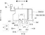
<実施形態1>
図1は、実施形態1に係るコネクタシールドの取付構造1の上面図である。図2は、実施形態1に係るコネクタシールドの取付構造1の正面図であり、図1におけるA矢視図である。図3は、実施形態1に係るコネクタシールドの取付構造1の左側面図であり、図1におけるB矢視図である。図4は、実施形態1に係るコネクタシールドの取付構造1の右側面図であり、図1におけるC矢視図である。<
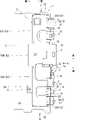
FIG. 1 is a top view of a connector
符号2は、例えば電子機器の金属製ハウジング(筐体)に収容される配線基板であり、その上面2Aに複数のコネクタ3が載置された状態で横並びに配列されている。図1~図4に示す例では、配線基板2の一部のみが図示されている。また、図1および図2に示す例では、配線基板2の上面2Aに7個のコネクタ3が並んでいる。なお、符号2Bは、配線基板2の下面である。 Numeral 2 denotes a wiring board housed in, for example, a metal housing (case) of an electronic device, and a plurality of
配線基板2は、例えば、PCB(Printed Circuit Board:プリント回路板)である
が、特に限定されない。また、配線基板2の上面2Aに実装されている各コネクタ3は、例えば、リフロー方式によって配線基板2に半田付けされている。また、各コネクタ3は、相手コネクタ(図示せず)を差し込み可能な差込口30を有する。The
以下においては、説明の便宜上、配線基板2に対して垂直な方向を上下方向とし、コネクタ3に相手コネクタが差し込まれる方向を前後方向とし、上下方向および前後方向に対して直交する方向を左右方向(横方向)とする。また、本明細書において用いる上下前後左右の各方向は、コネクタシールドの取付構造1を説明する上で各構成同士の相対的な位置関係を示すものに過ぎない。 Hereinafter, for convenience of explanation, the direction perpendicular to the
コネクタ3は、箱型に形成され、上面としての上壁部31と、下面としての下壁部32と、一対(左右)の側面としての側壁部33と、後面としての後壁部34を有する。コネクタ3は、上壁部31、下壁部32、一対の側壁部33に囲まれる収容空間に相手コネクタを受け入れることが可能であり、これらの前方端に形成された開口部が差込口30として機能する。コネクタ3の収容空間には、例えば、配線基板2に形成された配線と電気的に接続された接続端子が配置されている。コネクタ3には、前面の差込口30から相手コネクタが差し込まれ、コネクタ3の端子と相手コネクタの端子とが電気的に接続されるようになっている。なお、コネクタ3の上壁部31、下壁部32、側壁部33、後壁部34は、金属製のコネクタハウジングである。 The
図1~図4に示す符号5は、コネクタ3の外面を覆うことで当該コネクタ3を電磁遮断するためのコネクタシールドである。コネクタシールド5は、配線基板2および金属製ハウジングに導通して固定され、配線基板2に実装された電子部品(図示せず)で発生したノイズがコネクタ3を介して外部に伝達されることを抑制する。
本実施形態において、コネクタシールド5は、コネクタ3の前後方向における中央部付近から後方側に位置する外面を覆うように設けられている。図5は、実施形態1に係る配線基板2に実装されたコネクタ3の上面図であり、コネクタシールド5が配置される前の状態を示している。一方、図1~図4に示す状態において、コネクタシールド5が配線基板2に固定された状態を示している。また、図1、図2、図5等において、一部のコネクタ3における側壁部33等の符号について表記を省略している。 In the present embodiment, the
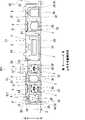
図6~図10は、実施形態1に係るコネクタシールド5の外観図である。図6は、実施形態1に係るコネクタシールド5の斜視図である。図7は、実施形態1に係るコネクタシールド5の上面図である。図8は、実施形態1に係るコネクタシールド5の背面図(後面図)である。図9は、実施形態1に係るコネクタシールド5の左側面図である。図10は
、実施形態1に係るコネクタシールド5の右側面図である。6 to 10 are external views of the
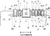
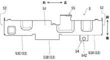
コネクタシールド5は、金属製の板材を例えばプレス加工および曲げ加工等することで形成されている。なお、コネクタシールド5は、複数の金属製の板材を接合することで形成することもできる。詳細構造については後述するが、コネクタシールド5は、コネクタ3の上壁部31(上面)を覆うための上板部51と、コネクタ3の側壁部33を覆うための一対の側板部52と、コネクタ3の後壁部34を覆うための後板部53等を有している。また、図6に示すように、コネクタシールド5は正面視コ字形をなしており、略矩形状を有する上板部51の横幅方向における両端から一対の側板部52が下方に向けて垂設されている。また、上板部51の後端からは後板部53が下方に向けて垂設されている。また、コネクタシールド5の正面側は、コネクタ3の差込口30が露出するように開放されている。 The
本実施形態において、コネクタシールド5は、配線基板2の上面2Aに一列に配列される複数のコネクタ3をまとめて電磁遮蔽するように設計されている。より具体的には、コネクタシールド5における上板部51は、配線基板2上に一列に並んでいる7個のコネクタ3の上壁部31をまとめて覆うために適した横幅を有している。但し、配線基板2に実装されるコネクタ3の数は特に限定されない。 In this embodiment, the
ここで、配線基板2の上面2Aに一列に配列される複数のコネクタ3(コネクタ群)のうち、その配列方向(以下、「コネクタ配列方向」という)における両端に位置するコネクタ3を、端部コネクタ3Aと呼ぶ(図1、図5等を参照)。コネクタシールド5における一対の側板部52は、各端部コネクタ3Aにおける一対の側壁部33のうち、コネクタ配列方向において外側に配置された側壁部33(以下、「外方側壁部33A」という)を覆うように構成されている(図1を参照)。 Here, among the plurality of connectors 3 (connector group) arranged in a row on the
図6、図9、図10等に示すように、コネクタシールド5における一対の側板部52の下端縁側には、各側板部52を配線基板2に取り付けるための取付部6が設けられている。各側板部52に設けられた取付部6の詳細構造については後述するが、各取付部6は配線基板2に設けられたスリット貫通孔20(図5を参照)と係合することで位置決め固定されるように構成されている。 As shown in FIGS. 6, 9, 10, etc., mounting
スリット貫通孔20は、配線基板2を貫通するスリット状の長孔であり、配線基板2に実装されたコネクタ3の前後方向に沿って延設されている。ここで、スリット貫通孔20が、コネクタ3の前後方向(配線基板2の前後方向ということもできる)に沿って延伸する延伸方向の寸法を「スリット長さ寸法Ls」と呼ぶ。また、スリット貫通孔20は、図5に示すように、一対の端部コネクタ3Aにおける外方側壁部33Aの近傍、具体的にはコネクタ配列方向において外方側壁部33Aよりも僅かに外側の位置に配置されている。図1~図4は、コネクタシールド5における左右一対の取付部6が配線基板2のスリット貫通孔20に係合した状態を示している。 The slit through
上記のように、配線基板2にコネクタシールド5が固定された状態では、上板部51がコネクタ3の上壁部31における中央付近から後方部分を覆い、一対の側板部52が端部コネクタ3Aにおける外方側壁部33Aを覆い、後板部53がコネクタ3の後壁部34を覆う。より詳しくは、コネクタシールド5の上壁部31は、コネクタ3を挟んで配線基板2の上面2Aに対向して配置される。また、コネクタシールド5の各側板部52は、端部コネクタ3Aにおける外方側壁部33Aに対向して配置され、後板部53がコネクタ3の後壁部34に対向して配置される。なお、本実施形態において、コネクタシールド5における後板部53は、3つの領域に分割された第1後板領域53A、第2後板領域53B、第3後板領域53Cによって形成されているが、これには限定されない。 As described above, in the state where the
図2~図5等に示すように、配線基板2に実装された各コネクタ3の上壁部31(上面)には、アースバネ4が設けられている。アースバネ4は、コネクタシールド5における上板部51の内面511(図2を参照)と、コネクタ3における上壁部31との間に介在する金属製の板バネ部材である。コネクタシールド5がコネクタ3の外面を覆うように配線基板2に固定された状態において、アースバネ4は、コネクタシールド5における上板部51の内面511と弾性接触している。アースバネ4は、コネクタ3における上壁部31の一部を斜めに切り起すことで形成されており、上壁部31から上斜め後方に向けて延在している(図3、図4において破線で示されるアースバネ4を参照)。 As shown in FIGS. 2 to 5 and the like, a
コネクタシールド5がコネクタ3の外面を覆うように設置される際、アースバネ4が上板部51の内面511によって下方に押圧されることで、アースバネ4が弾性変形する。その結果、アースバネ4とコネクタシールド5との間の電気的導通が確保される。なお、本実施形態において、コネクタシールド5における上板部51の内面511とコネクタ3における上壁部31との間にアースバネ4が介在していれば良い。よって、アースバネ4は、コネクタシールド5における上板部51の内面511側に設けられていても良い。 When the
また、図3、図4、図7、図8等に示すように、コネクタシールド5の後板部53における第1後板領域53Aの下端には、当該後板部53における第1後板領域53Aを配線基板2にネジ止めするための第1ネジ止め固定部54が設けられている。第1ネジ止め固定部54は、例えば、矩形状を有する金属製の平板片であり、後板部53における第1後板領域53Aの下端縁から直交方向に屈曲し、上板部51と略平行に延在する。第1ネジ止め固定部54の下面541は、配線基板2にコネクタシールド5が取り付けられた状態で、配線基板2の上面2Aに沿って配置され、上面2Aに当接するように形成されている。 3, 4, 7, 8, etc., at the lower end of the first
また、図7および図8等に示すように、第1ネジ止め固定部54には、ネジ止め用のネジ71(図1を参照)の軸部を挿通可能な第1ネジ挿通孔542が、第1ネジ止め固定部54を貫通するように形成されている。また、図5に示すように、配線基板2には、第1ネジ挿通孔542を挿通させたネジ71を螺合可能なネジ溝を有するネジ止め孔21が設けられている。第1ネジ止め固定部54における第1ネジ挿通孔542に挿通させたネジ71をネジ止め孔21に螺合させることで、コネクタシールド5を配線基板2に固定すると共に、コネクタシールド5と配線基板2の電気的導通を確保することができる。なお、本実施形態においては、後板部53における第1後板領域53Aに第1ネジ止め固定部54を配設するようにしているが、第1ネジ止め固定部54を後板部53における第2後板領域53B又は第3後板領域53Cに配設しても良い。 7 and 8, etc., the first
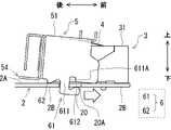
更に、コネクタシールド5は、上板部51における前端縁の適所に第2ネジ止め固定部55が設けられている。第2ネジ止め固定部55には、ネジ(図示せず)を螺合可能なネジ溝を有するネジ止め孔551(図6、図8等を参照)が、第2ネジ止め固定部55を貫通するように形成されている。第2ネジ止め固定部55は、例えば、コネクタシールド5の上板部51における前端縁から垂直方向上側に向かって屈曲するように延在する金属片である。そして、金属製ハウジング(図示せず)の所定箇所に形成されたネジ挿通孔にネジを挿通させつつ、第2ネジ止め固定部55におけるネジ止め孔551にネジを螺合させる。これにより、コネクタシールド5と金属製ハウジングの電気的導通を確保できる。 Further, the
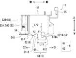
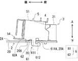
次に、コネクタシールド5における一対の側板部52の下端縁521に設けられた取付部6の詳細と、取付部6を用いたコネクタシールド5の取付構造について説明する。なお、各側板部52に設けられた取付部6は同一構造である。取付部6は、抜け止め部61および位置決め用突片62を有する。抜け止め部61は、側板部52の下端縁521の前後
方向における中央付近から下方に向けて突設された足部611と、当該足部611の先端から前方に向けて突設された係止用フック部612を含む。ここで、符号611Aは、足部611の前側端面である。また、符号611Bは、足部611の後側端面である。また、符号62Aは、位置決め用突片62の後側端面である。Next, the details of the mounting
各側板部52における下端縁521のうち、抜け止め部61の足部611が突設されている位置を「第1の位置P1」と呼び、位置決め用突片62が突設されている位置を「第2の位置P2」と呼ぶ。また、各側板部52の前後方向において、抜け止め部61の足部611から係止用フック部612が突設される方向を「第1の方向D1」と呼び、その反対方向を「第2の方向D2」と呼ぶ。本実施形態では、側板部52における前方側が「第1の方向D1」に相当し、側板部52における後方側が「第2の方向D2」に相当する。 The position where the
取付部6における位置決め用突片62は、各側板部52の下端縁521のうち、抜け止め部61の足部611が下方に突設された第1の位置P1から第2の方向D2(足部611から係止用フック部612が突出する方とは反対の方向)にずれた第2の位置P2から下方に向けて突設されている。具体的には、抜け止め部61の足部611から係止用フック部612が前方に向かって突出し、側板部52における足部611よりも後方側の位置に位置決め用突片62が設けられている。 The
図9および図10に示す符号Lf1は、抜け止め部61が側板部52の前後方向に沿って延在する長さ寸法であり、以下では「第1長さ寸法Lf1」と呼ぶ。また、符号Lf2は、取付部6における足部611の前側端面611Aから位置決め用突片62の後側端面62Aまでの、側板部52の前後方向に沿った長さ寸法であり、以下では「第2長さ寸法Lf2」と呼ぶ。ここで、第1長さ寸法Lf1は、スリット貫通孔20におけるスリット長さ寸法Lsよりも小さい。これにより、取付部6における抜け止め部61を、スリット貫通孔20に対して容易に挿入することができる。 Reference character Lf1 shown in FIGS. 9 and 10 is a length dimension in which the retaining
また、第2長さ寸法Lf2は、スリット貫通孔20におけるスリット長さ寸法Lsに比べて僅かに小さな寸法に設計されている。これにより、取付部6における抜け止め部61および位置決め用突片62をスリット貫通孔20に挿入した際、スリット貫通孔20の前端孔壁面20Aに足部611の前側端面611Aを係合(当接)させ、スリット貫通孔20の後端孔壁面20Bに位置決め用突片62の後側端面62Aを係合(当接)させることができる。その結果、スリット貫通孔20の前後方向において取付部6が位置決めされ、スリット貫通孔20の延在方向への抜け止め部61のスライド移動が規制される。なお、コネクタシールド5を製造する際の各部の寸法に製造誤差が生じたとしても、第2長さ寸法Lf2がスリット長さ寸法Lsよりも大きくならないように、双方の基準寸法及び寸法公差を設計することが好ましい。例えば、第2長さ寸法Lf2及びスリット長さ寸法Lsの基準寸法を6mmとした場合に、第2長さ寸法Lf2における最大許容寸法を6.0mm、最小許容寸法を5.9mmとし、スリット長さ寸法Lsの最大許容寸法を6.2mm、最小許容寸法を6.1mmとしても良い。このようにすることで、コネクタシールド5の取付部6をスリット貫通孔20に取り付ける際、位置決め用突片62がスリット貫通孔20に挿入しにくくなることを抑制できる。 Also, the second length dimension Lf2 is designed to be slightly smaller than the slit length dimension Ls in the slit through-
図9および図10における符号521Aは、側板部52の下端縁521における「第1下端縁領域」を示す。第1下端縁領域521Aは、側板部52における下端縁521のうち、足部611が突設される第1の位置P1よりも、第1の方向D1側に位置する領域である。ここで、側板部52の第1下端縁領域521Aにおける上板部51からの高さ方向の寸法を「第1高さ寸法H1」と定義する。また、上板部51から第1ネジ止め固定部54における下面541までの高さ方向の寸法を「第2高さ寸法H2」と定義する。本実施形態においては、第1高さ寸法H1が第2高さ寸法H2よりも小さい(図9および図10
を参照)。
).
図11A~図11Cは、実施形態1に係るコネクタシールド5の配線基板2に対する取付方法を説明する図である。以下、取付部6を用いてコネクタシールド5を配線基板2に取り付ける(組み付ける)手順について詳しく説明する。なお、図11A~図11Cにおいては、便宜上、コネクタシールド5における第2ネジ止め固定部55の図示を省略している。 11A to 11C are diagrams for explaining how to attach the
(第1ステップ)
配線基板2にコネクタシールド5を取り付ける場合、まず、図11Aに示すように、各側板部52に設けられた取付部6の抜け止め部61を、配線基板2のスリット貫通孔20に挿入する。抜け止め部61が前後方向に延在する第1長さ寸法Lf1は、スリット貫通孔20におけるスリット長さ寸法Lsに比べて小さいため、取付部6における抜け止め部61を配線基板2のスリット貫通孔20に対して容易に挿入できる。スリット貫通孔20に取付部6の抜け止め部61を挿入する際、図11Aに示すように、コネクタシールド5の正面側が下方に傾いた姿勢とすることで、スリット貫通孔20に対して抜け止め部61を入し易くなる。(first step)
When attaching the
(第2ステップ)
取付部6の抜け止め部61をスリット貫通孔20に挿入後、次いで、図11Bに示すようにコネクタシールド5を前方に向けてスライドさせる。その結果、抜け止め部61における足部611がスリット貫通孔20に沿って前端孔壁面20Aに近づく方向へスライドする。その際、抜け止め部61の係止用フック部612が配線基板2の下面2B側に潜り込むようにスリット貫通孔20に沿って足部611をスライドさせることで、スリット貫通孔20の縁部に係止用フック部612が係止される。(second step)
After inserting the retaining
ここで、図11Bに示すように、抜け止め部61における足部611の前側端面611Aがスリット貫通孔20の前端孔壁面20Aに当接すると、足部611のそれ以上のスライド移動が規制される。このように、抜け止め部61における足部611の前側端面611Aがスリット貫通孔20の前端孔壁面20Aに当接した状態を「第1位置決め状態」という。なお、第1位置決め状態では、取付部6における位置決め用突片62が未だスリット貫通孔20に挿入されていない。 Here, as shown in FIG. 11B, when the
また、本実施形態においては、第1高さ寸法H1が第2高さ寸法H2よりも小さな寸法に設定されている。そのため、例えば、製造誤差等に起因して配線基板2の基板厚さが設計寸法よりも多少大きくても、側板部52における第1下端縁領域521Aを配線基板2の上面2Aと干渉させることなく、抜け止め部61の足部611をスリット貫通孔20に沿って円滑にスライドさせることができる。 Moreover, in this embodiment, the first height dimension H1 is set to be smaller than the second height dimension H2. Therefore, for example, even if the board thickness of the
また、本実施形態においては、コネクタ3の上壁部31にアースバネ4が配置されているため、アースバネ4の弾性力(付勢力)によって、コネクタシールド5の後方側が上方に浮き上がる反面、コネクタシールド5の前方側が下方に大きく傾斜する場合がある。その場合においても、側板部52における第1下端縁領域521Aの前端部がストッパーとして機能し、配線基板2の上面2Aに第1下端縁領域521Aの前端部が当接することで、コネクタシールド5の姿勢が過度に傾くことを抑制できる。 Further, in this embodiment, since the
(第3ステップ)
また、本実施形態においては、第2長さ寸法Lf2がスリット貫通孔20におけるスリット長さ寸法Lsと等しい。そのため、図11Bに示す第1位置決め状態においては、スリット貫通孔20の後端孔壁面20Bの直上に位置決め用突片62の後側端面62Aが位
置している。そこで、アースバネ4のバネ力に抗してコネクタシールド5の後方側を下方に押し下げることで、図11Cに示すように、取付部6における位置決め用突片62をスリット貫通孔20に挿入させる。(Third step)
Also, in the present embodiment, the second length dimension Lf2 is equal to the slit length dimension Ls in the slit through-
このようにして、取付部6における位置決め用突片62がスリット貫通孔20に挿入されると、抜け止め部61における係止用フック部612がスリット貫通孔20の縁部(具体的には、スリット貫通孔20の縁部を形成する下面2B)に係止された状態で、スリット貫通孔20に挿入された位置決め用突片62および足部611がスリット貫通孔20の孔壁面と係合する。すなわち、スリット貫通孔20の前端孔壁面20Aに対して足部611の前側端面611Aが係合(当接)し、且つ、スリット貫通孔20の後端孔壁面20Bに対して位置決め用突片62の後側端面62Aが係合(当接)する。そのため、スリット貫通孔20の延在方向(長手方向)に沿った抜け止め部61のスライドを規制することができる。また、抜け止め部61における係止用フック部612がスリット貫通孔20の縁部に係止されることで、スリット貫通孔20からの抜け止め部61の抜け出しも規制することができる。以上より、スリット貫通孔20の延在方向(長手方向)および抜け出し方向への取付部6の動きが規制される結果、コネクタシールド5の上板部51を押し上げる方向に作用するアースバネ4の反発力に抗して、スリット貫通孔20に取付部6を位置決めした状態で固定できる(以下、この状態を「位置決め固定状態」という)。なお、図11Cに示す符号612Aは、抜け止め部61における係止用フック部612の基板当接部である。係止用フック部612の基板当接部612Aは、コネクタシールド5を位置決め固定状態とした状態で配線基板2の下面2Bに当接する部分である。図11に示す符号A1で表されるハッチング領域は、配線基板2の下面2Bのうち、位置決め固定状態にあるコネクタシールド5の係止用フック部612における基板当接部612Aが当接するフック当接領域である。配線基板2の下面2Bにおけるフック当接領域A1は、例えば、レジストで被覆せずに銅箔を露出させていても良い。これによれば、係止用フック部612における基板当接部612Aと配線基板2におけるフック当接領域A1との電気的導通を確保することができ、コネクタシールド5と配線基板2との電気的導通を強化することができる。 In this way, when the
また、上記の位置決め固定状態では、アースバネ4の反発力を利用して、抜け止め部61の係止用フック部612を配線基板2の下面2Bに対して押し付けた状態に維持することができる。これによれば、側板部52における第1下端縁領域521Aと配線基板2における上面2Aとの間に隙間が設けられていても、コネクタシールド5にガタツキが生じることを抑制できる。これにより、配線基板2の上面2Aに対してコネクタシールド5の上板部51が平行に配置された姿勢にコネクタシールド5を保持することができる。 In the positioning and fixing state described above, the repulsive force of the
以上のように、コネクタシールド5の取付構造によれば、コネクタシールド5を配線基板2に対して容易に取り付ける(組み付ける)ことができる。そして、配線基板2に対するコネクタシールド5の組み付けが完了した後は、コネクタシールド5における後板部53に設けられた第1ネジ止め固定部54を配線基板2に対してネジ止めする。その結果、配線基板2に対してコネクタシールド5を完全に固定することができ、且つ、コネクタシールド5と配線基板2の電気的導通を確保できる。なお、配線基板2への取付部6を用いたコネクタシールド5の組み付けは、配線基板2に対するコネクタシールド5の仮止めということもできる。 As described above, according to the mounting structure of the
本実施形態におけるコネクタシールド5の取付構造によれば、コネクタシールド5を配線基板2に組み付けた(仮止めした)状態において、抜け止め部61の係止用フック部612がスリット貫通孔20の縁部(配線基板2の下面2B)に係止されているため、コネクタシールド5を配線基板2にネジ止めする際、治具を用いてコネクタシールド5を配線基板2に押さえ付けておく必要がない。従って、電子機器を製造する際の工数を減らすこ
とができる。また、上記のように、治具を用いてコネクタシールド5を配線基板2に押さえ付けなくても、配線基板2からのコネクタシールド5の浮き上がりを抑制できるため、コネクタシールド5を配線基板2に組み付ける工程とネジ止めする工程とを分離することができる。よって、電子機器を製造する製造工程の自由度を高めることができる。According to the mounting structure of the
また、本実施形態におけるコネクタシールド5の取付構造によれば、コネクタシールド5における側板部52を配線基板2にネジ止めする必要がないため、コネクタシールド5を配線基板2に固定する際の作業性が非常に優れている。また、配線基板2に対するネジ止め箇所が1か所だけでも、配線基板2にするコネクタシールド5の浮き上がりを抑制しつつ、コネクタシールド5とコネクタ3の間の電気的導通を確保することができる。また、配線基板2上に多数のコネクタ3が一列に配列している場合等のように、端部のコネクタ3の側方にネジ止めするスペースが確保できない状況においても、配線基板2に対してコネクタシールド5を好適に固定することができる。 In addition, according to the mounting structure of the
なお、本実施形態においては、配線基板2の上面2Aに一列に配列される複数のコネクタ3を一纏めとしてコネクタシールド5で電磁遮蔽する例を説明したが、これには限定されない。例えば、コネクタシールド5は、単一のコネクタ3を単独で覆うことにより、電磁遮蔽しても良い。その場合、コネクタシールド5における上板部51は、特定のコネクタ3における上壁部31を覆い、一対の側板部52は当該特定のコネクタ3における各側壁部33を覆うように配置されうる。但し、配線基板2の上面2Aに複数のコネクタ3が一列に配列される場合には、上記のように端部のコネクタ3の側方にネジ止めするスペースを十分に確保できない状況になり易い。よって、そのような条件下で本実施形態に係るコネクタシールド5の取付構造を適用することで、上述した技術的効果をより一層顕著に得ることができる。 In the present embodiment, an example has been described in which a plurality of
<実施形態2>
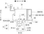
次に、実施形態2に係るコネクタシールド5Aを説明する。実施形態2に係るコネクタシールド5Aは、各側板部52の下端縁521に設けられた取付部6の抜け止め部61および位置決め用突片62の位置関係だけが実施形態1に係るコネクタシールド5と相違する。以下、実施形態2に係るコネクタシールド5Aについて、実施形態1に係るコネクタシールド5との相違点を中心に説明する。図12は、実施形態2に係るコネクタシールド5Aの左側面図である。図13は、実施形態2に係るコネクタシールド5Aの右側面図である。図12および図13において、実施形態1に係るコネクタシールド5と同一の構成については、同一の符号を付すことで詳しい説明を省略する。<
Next, a
図12および図13に示すように、実施形態2に係るコネクタシールド5Aは、各側板部52の下端縁521において、取付部6の抜け止め部61および位置決め用突片62の前後関係が実施形態1のコネクタシールド5と入れ替わっている。すなわち、側板部52の下端縁521において、位置決め用突片62の後方側に抜け止め部61が配置されている。そして、図12および図13に示すように、側板部52の下端縁521における第1の位置P1から抜け止め部61の足部611が下方に突設され、当該足部611の下端から係止用フック部612が第1の方向D1に突設されている。実施形態2に係るコネクタシールド5Aでは、第1の方向D1が側板部52における後方側に対応しており、抜け止め部61の係止用フック部612が足部611の下端から後方に向かって突設されている。また、側板部52の下端縁521のうち、抜け止め部61の足部611が突設された第1の位置P1から、第2の方向D2(本実施形態では、側板部52における前方側に対応)にずれた第2の位置P2から位置決め用突片62が下方に向けて突設されている。なお、符号62Bは、位置決め用突片62の前側端面である。 As shown in FIGS. 12 and 13, in the
ここで、 図12および図13に示す符号Lf1は、実施形態1と同様、抜け止め部6
1が側板部52の前後方向に沿って延在する「第1長さ寸法」である。符号Lf2´は、取付部6における足部611の後側端面611Bから位置決め用突片62の前側端面62Bまでの、側板部52の前後方向に沿った「第2長さ寸法」である。実施形態2においても、実施形態1と同様、第1長さ寸法Lf1が配線基板2に形成されているスリット貫通孔20(図5を参照)におけるスリット長さ寸法Lsよりも小さい。これにより、取付部6における抜け止め部61を、配線基板2のスリット貫通孔20に挿入することができる。また、第2長さ寸法Lf2´は、スリット貫通孔20におけるスリット長さ寸法Lsと等しい。12 and 13 is the retaining
1 is the “first length dimension” that extends along the front-rear direction of the
以上のように構成されるコネクタシールド5Aは、実施形態1に係るコネクタシールド5と基本的に同様の手順で、取付部6における抜け止め部61および位置決め用突片62を配線基板2のスリット貫通孔20に挿入し、係合させることでコネクタシールド5Aを配線基板2に取り付けることができる。 The
すなわち、配線基板2のスリット貫通孔20に対して、コネクタシールド5Aの取付部6における抜け止め部61を挿入した後、抜け止め部61の係止用フック部612が配線基板2の下面2B側に潜り込むようにコネクタシールド5Aをスライドさせる。その際、本実施形態においては、コネクタシールド5を後方に向けてスライドさせることで、抜け止め部61における足部611を、スリット貫通孔20に沿って後端孔壁面20Bに近づく方向へスライドさせる。そして、スリット貫通孔20の後端孔壁面20B(図5を参照)に足部611の後側端面611Bが当接した時点で、取付部6における位置決め用突片62をスリット貫通孔20に挿入させる。ここで、コネクタシールド5Aにおいては、第2長さ寸法Lf2´がスリット貫通孔20におけるスリット長さ寸法Lsと等しい寸法に設定されているため、抜け止め部61における足部611の後側端面611Bがスリット貫通孔20の後端孔壁面20Bに当接した状態からアースバネ4のバネ力に抗してコネクタシールド5Aの前方側を下方に押し下げることで、取付部6における位置決め用突片62をスリット貫通孔20に円滑に挿入できる。 That is, after the retaining
上記のようにして、取付部6における抜け止め部61および位置決め用突片62が配線基板2のスリット貫通孔20に挿入されると、スリット貫通孔20の後端孔壁面20Bに足部611の後側端面611Bが係合(当接)し、且つ、スリット貫通孔20の前端孔壁面20Aに位置決め用突片62の前側端面62Bが係合(当接)することで、スリット貫通孔20の延在方向(長手方向)に沿った抜け止め部61のスライドが規制することができる。また、抜け止め部61における係止用フック部612がスリット貫通孔20の縁部に係止されることで、スリット貫通孔20からの抜け止め部61の抜け出しも規制することができる。以上より、スリット貫通孔20の延在方向(長手方向)および抜け出し方向への取付部6の動きが規制される結果、スリット貫通孔20に取付部6を位置決め固定することができる。その結果、実施形態2に係るコネクタシールド5Aの取付構造においても、実施形態1と同様の効果が得られる。 When the retaining
以上、本発明の実施の形態を説明したが、本発明はこれらに限定されるものではなく、上記構成を組み合わせるなど、特許請求の範囲の趣旨を逸脱しない限りにおいて、当業者の知識に基づく種々の変更が可能である。例えば、上述までの実施形態において、配線基板2に一対のスリット貫通孔20を配置し、各スリット貫通孔20に取付部6の抜け止め部61および位置決め用突片62の双方をまとめて挿入する態様を例に説明したが、これには限られない。例えば、各スリット貫通孔20は、取付部6の抜け止め部61を挿入するための第1領域と、位置決め用突片62を挿入するための第2領域が個別に独立して設けられていても良い。 Although the embodiments of the present invention have been described above, the present invention is not limited to these, and various modifications based on the knowledge of those skilled in the art, such as combining the above configurations, as long as they do not deviate from the spirit of the claims. can be changed. For example, in the above-described embodiments, a pair of slit through-
1・・・コネクタシールドの取付構造
2・・・配線基板
3・・・コネクタ
4・・・アースバネ
5・・・コネクタシールド
6・・・取付部
20・・・スリット貫通孔
31・・・上壁部
32・・・下壁部
33・・・側壁部
34・・・後壁部
51・・・上板部
52・・・側板部
53・・・後板部
61・・・抜け止め部
62・・・位置決め用突片
611・・・足部
612・・・係止用フック部
Claims (4)
Translated fromJapanese前記コネクタシールドは、
前記コネクタの上面を覆う上板部と、
前記コネクタの側面を覆う、前記上板部の両側端から下方に延設された一対の側板部と、
各側板部の下端縁側に設けられ、各側板部を前記配線基板に取り付ける取付部と、
を備え、
前記配線基板は、各側板部の前記取付部を位置決め固定するスリット貫通孔を有し、
前記コネクタシールドおよび前記コネクタの間にはアースバネが介在し、
前記取付部は、
前記側板部の下端縁の第1の位置から下方に突設された足部と、当該足部から前方又は後方の第1の方向に突設された係止用フック部と、を有する、前記スリット貫通孔に挿入可能な抜け止め部と、
前記側板部の下端縁のうち、前記第1の位置から前記第1の方向と反対の第2の方向にずれた第2の位置から下方に突設された、前記スリット貫通孔に挿入可能な位置決め用突片と、
を有し、
前記スリット貫通孔に挿入された前記係止用フック部が前記スリット貫通孔の縁部に係止され、且つ、前記スリット貫通孔に挿入された前記位置決め用突片および前記足部が前記スリット貫通孔の孔壁面と係合することで、前記取付部が前記スリット貫通孔に位置決め固定される、
コネクタシールドの取付構造。A mounting structure for a connector shield mounted on a wiring board and covering a connector having an insertion port for a mating connector on the front surface thereof, comprising:
The connector shield is
an upper plate portion covering the upper surface of the connector;
a pair of side plate portions extending downward from both side ends of the upper plate portion covering side surfaces of the connector;
a mounting portion provided on a lower edge side of each side plate portion for mounting each side plate portion to the wiring substrate;
with
The wiring board has a slit through hole for positioning and fixing the mounting portion of each side plate portion,
A ground spring is interposed between the connector shield and the connector,
The mounting portion is
The foot portion projecting downward from a first position on the lower edge of the side plate portion, and the locking hook portion projecting forward or backward in a first direction from the foot portion. a retaining portion that can be inserted into the slit through-hole;
It can be inserted into the slit through-hole projecting downward from a second position shifted in a second direction opposite to the first direction from the first position in the lower edge of the side plate portion. a positioning protrusion;
has
The locking hook portion inserted into the slit through hole is locked to the edge portion of the slit through hole, and the positioning protrusion and the foot portion inserted into the slit through hole penetrate the slit. By engaging with the hole wall surface of the hole, the mounting portion is positioned and fixed to the slit through hole,
Mounting structure of the connector shield.
前記コネクタの後面を覆うための後板部と、
前記後板部に設けられ、前記配線基板にネジ止めされるネジ止め固定部と、
を更に備える、
請求項1に記載のコネクタシールドの取付構造。The connector shield is
a rear plate portion for covering the rear surface of the connector;
a screw fixing portion provided on the rear plate portion and screwed to the wiring board;
further comprising
The mounting structure of the connector shield according to claim 1.
請求項2に記載のコネクタシールドの取付構造。Among the lower edges of the side plate portions, a first lower edge region located on the first direction side of the first position has a first height dimension from the upper plate portion that is greater than the upper plate portion. smaller than the second height dimension to the lower surface of the screw fixing part,
The mounting structure of the connector shield according to claim 2.
一対の前記側板部は、複数の前記コネクタの配列方向において両端に位置するコネクタの側面を覆う、
請求項1から3の何れか一項に記載のコネクタシールドの取付構造。the upper plate portion of the connector shield has a width that collectively covers the upper surfaces of the plurality of connectors arranged in a row on the wiring board;
The pair of side plate portions cover the side surfaces of the connectors located at both ends in the arrangement direction of the plurality of connectors,
The connector shield mounting structure according to any one of claims 1 to 3.
Priority Applications (2)
| Application Number | Priority Date | Filing Date | Title |
|---|---|---|---|
| JP2019136431AJP7203700B2 (en) | 2019-07-24 | 2019-07-24 | Connector shield mounting structure |
| US16/813,985US11069993B2 (en) | 2019-07-24 | 2020-03-10 | Mounting structure of connector shield |
Applications Claiming Priority (1)
| Application Number | Priority Date | Filing Date | Title |
|---|---|---|---|
| JP2019136431AJP7203700B2 (en) | 2019-07-24 | 2019-07-24 | Connector shield mounting structure |
Publications (2)
| Publication Number | Publication Date |
|---|---|
| JP2021022436A JP2021022436A (en) | 2021-02-18 |
| JP7203700B2true JP7203700B2 (en) | 2023-01-13 |
Family
ID=74187615
Family Applications (1)
| Application Number | Title | Priority Date | Filing Date |
|---|---|---|---|
| JP2019136431AActiveJP7203700B2 (en) | 2019-07-24 | 2019-07-24 | Connector shield mounting structure |
Country Status (2)
| Country | Link |
|---|---|
| US (1) | US11069993B2 (en) |
| JP (1) | JP7203700B2 (en) |
Citations (6)
| Publication number | Priority date | Publication date | Assignee | Title |
|---|---|---|---|---|
| JP2001196112A (en) | 2000-01-07 | 2001-07-19 | Alps Electric Co Ltd | Ic card connector |
| JP2009238621A (en) | 2008-03-27 | 2009-10-15 | Yazaki Corp | Shielded connector for printed circuit board |
| JP2011028851A (en) | 2009-07-21 | 2011-02-10 | Yazaki Corp | Shield case and connector with connector housing shielded by the same |
| JP2012054050A (en) | 2010-08-31 | 2012-03-15 | Yazaki Corp | Board-mounted connector |
| JP2016081591A (en) | 2014-10-10 | 2016-05-16 | 第一精工株式会社 | Electrical connector and electrical connector device |
| JP2019016514A (en) | 2017-07-06 | 2019-01-31 | 株式会社デンソーテン | Connector mounting structure and connector shield |
Family Cites Families (25)
| Publication number | Priority date | Publication date | Assignee | Title |
|---|---|---|---|---|
| JPH0716312Y2 (en)* | 1989-02-28 | 1995-04-12 | ホシデン株式会社 | connector |
| JPH0722064Y2 (en)* | 1989-12-04 | 1995-05-17 | ホシデン株式会社 | connector |
| US5221212A (en)* | 1992-08-27 | 1993-06-22 | Amp Incorporated | Shielding a surface mount electrical connector |
| JP2914616B2 (en)* | 1995-06-12 | 1999-07-05 | ソニー株式会社 | Connector socket |
| US5984725A (en)* | 1997-04-30 | 1999-11-16 | Berg Technology, Inc. | Filtered universal serial bus |
| JPH1167365A (en)* | 1997-08-08 | 1999-03-09 | Molex Inc | Electrical connector |
| US6083043A (en)* | 1998-12-28 | 2000-07-04 | Hon Hai Precision Ind. Co., Ltd. | Fastening device for an electrical connector |
| US6394846B1 (en)* | 1999-08-06 | 2002-05-28 | Fci Americas Technology, Inc. | Electrical connector with separate receptacles using common filter |
| TW484757U (en)* | 2000-06-03 | 2002-04-21 | Hon Hai Prec Ind Co Ltd | Electrical connector assembly |
| DE10102459B4 (en)* | 2001-01-15 | 2014-12-24 | Finisar Corp. | Housing for a plug-in with the housing connectable electrical component and method for mounting such a housing to a circuit board |
| US6419523B1 (en)* | 2001-04-04 | 2002-07-16 | Hon Hai Precision Ind. Co., Ltd. | Small form-factor pluggable transceiver cage |
| US6416361B1 (en)* | 2001-11-16 | 2002-07-09 | Hon Hai Precision Ind. Co., Ltd. | Small form-factor pluggable transceiver cage |
| US6478622B1 (en)* | 2001-11-27 | 2002-11-12 | Hon Hai Precision Ind. Co., Ltd. | Small form-factor pluggable transceiver cage |
| EP1982389A1 (en)* | 2006-01-30 | 2008-10-22 | Fci | Shell for circuit board connector |
| JP5080307B2 (en)* | 2008-02-15 | 2012-11-21 | 矢崎総業株式会社 | Shield connector |
| JP5160970B2 (en)* | 2008-06-16 | 2013-03-13 | 矢崎総業株式会社 | Shield connector |
| CN201590517U (en)* | 2009-11-30 | 2010-09-22 | 美国莫列斯股份有限公司 | Electric connector and electric connector combination |
| TWI508392B (en)* | 2010-03-26 | 2015-11-11 | Hosiden Corp | Shields, connectors and electronic machines |
| JP5622306B2 (en)* | 2010-07-05 | 2014-11-12 | 矢崎総業株式会社 | Board mounted connector |
| US8968031B2 (en)* | 2012-06-10 | 2015-03-03 | Apple Inc. | Dual connector having ground planes in tongues |
| US9425542B1 (en)* | 2015-08-20 | 2016-08-23 | Cheng Uei Precision Industry Co., Ltd. | Water-proof connector |
| KR102504107B1 (en)* | 2015-10-27 | 2023-02-27 | 삼성전자주식회사 | Multimedia interface connector and electronic device having the same |
| US10263365B2 (en)* | 2016-03-15 | 2019-04-16 | Aces Electronics Co., Ltd. | Plug unit and receptacle unit |
| CN107293890A (en)* | 2016-04-11 | 2017-10-24 | 连展科技(深圳)有限公司 | Electric connector for socket |
| CN107293874A (en)* | 2016-04-11 | 2017-10-24 | 连展科技(深圳)有限公司 | Electric connector for socket |
- 2019
- 2019-07-24JPJP2019136431Apatent/JP7203700B2/enactiveActive
- 2020
- 2020-03-10USUS16/813,985patent/US11069993B2/enactiveActive
Patent Citations (6)
| Publication number | Priority date | Publication date | Assignee | Title |
|---|---|---|---|---|
| JP2001196112A (en) | 2000-01-07 | 2001-07-19 | Alps Electric Co Ltd | Ic card connector |
| JP2009238621A (en) | 2008-03-27 | 2009-10-15 | Yazaki Corp | Shielded connector for printed circuit board |
| JP2011028851A (en) | 2009-07-21 | 2011-02-10 | Yazaki Corp | Shield case and connector with connector housing shielded by the same |
| JP2012054050A (en) | 2010-08-31 | 2012-03-15 | Yazaki Corp | Board-mounted connector |
| JP2016081591A (en) | 2014-10-10 | 2016-05-16 | 第一精工株式会社 | Electrical connector and electrical connector device |
| JP2019016514A (en) | 2017-07-06 | 2019-01-31 | 株式会社デンソーテン | Connector mounting structure and connector shield |
Also Published As
| Publication number | Publication date |
|---|---|
| US20210028565A1 (en) | 2021-01-28 |
| US11069993B2 (en) | 2021-07-20 |
| JP2021022436A (en) | 2021-02-18 |
Similar Documents
| Publication | Publication Date | Title |
|---|---|---|
| KR100635893B1 (en) | Connector having a simple structure assuring a stable mounting operation | |
| CN103633461B (en) | Connector assembly for connector system | |
| US7806702B2 (en) | Connector for an electric device such as a board | |
| JP7606661B2 (en) | PCB Connectors and Devices | |
| TWI552448B (en) | Connector | |
| CN108023206B (en) | Electronics and Connectors | |
| KR20210004828A (en) | Connector assembly | |
| CN104221227A (en) | Wire-to-board connectors | |
| CN104218367B (en) | Plug connector and manufacture method thereof | |
| JP7044736B2 (en) | Electronic component unit | |
| JP4976103B2 (en) | connector | |
| JP5235221B2 (en) | connector | |
| CN104218368B (en) | Plug connector and method of manufacturing the same | |
| JP2000182694A (en) | Board connection connector | |
| CN117616646A (en) | Connectors and machines for circuit boards | |
| CN221708972U (en) | Contact type connector | |
| JP7203700B2 (en) | Connector shield mounting structure | |
| US9755339B2 (en) | Connecting structure of connector and flat circuit body | |
| TWI891140B (en) | Contact type connector | |
| JP5884131B2 (en) | Flat flexible wiring connector | |
| JP5922325B2 (en) | Circuit board electrical connector | |
| JP2025122853A (en) | Floating Connector | |
| JP6967974B2 (en) | Mounting structure of connector housing | |
| JP2021182486A (en) | Connector and connector unit | |
| JP2024019779A (en) | connector |
Legal Events
| Date | Code | Title | Description |
|---|---|---|---|
| A621 | Written request for application examination | Free format text:JAPANESE INTERMEDIATE CODE: A621 Effective date:20220331 | |
| A977 | Report on retrieval | Free format text:JAPANESE INTERMEDIATE CODE: A971007 Effective date:20221128 | |
| TRDD | Decision of grant or rejection written | ||
| A01 | Written decision to grant a patent or to grant a registration (utility model) | Free format text:JAPANESE INTERMEDIATE CODE: A01 Effective date:20221213 | |
| A61 | First payment of annual fees (during grant procedure) | Free format text:JAPANESE INTERMEDIATE CODE: A61 Effective date:20221227 | |
| R150 | Certificate of patent or registration of utility model | Ref document number:7203700 Country of ref document:JP Free format text:JAPANESE INTERMEDIATE CODE: R150 |