JP7202557B2 - Stencil step design method, system, computer readable storage medium and device - Google Patents
Stencil step design method, system, computer readable storage medium and deviceDownload PDFInfo
- Publication number
- JP7202557B2 JP7202557B2JP2021555522AJP2021555522AJP7202557B2JP 7202557 B2JP7202557 B2JP 7202557B2JP 2021555522 AJP2021555522 AJP 2021555522AJP 2021555522 AJP2021555522 AJP 2021555522AJP 7202557 B2JP7202557 B2JP 7202557B2
- Authority
- JP
- Japan
- Prior art keywords
- stencil
- opening
- electronic component
- design
- data
- Prior art date
- Legal status (The legal status is an assumption and is not a legal conclusion. Google has not performed a legal analysis and makes no representation as to the accuracy of the status listed.)
- Active
Links
Images


Classifications
- H—ELECTRICITY
- H05—ELECTRIC TECHNIQUES NOT OTHERWISE PROVIDED FOR
- H05K—PRINTED CIRCUITS; CASINGS OR CONSTRUCTIONAL DETAILS OF ELECTRIC APPARATUS; MANUFACTURE OF ASSEMBLAGES OF ELECTRICAL COMPONENTS
- H05K3/00—Apparatus or processes for manufacturing printed circuits
- H05K3/0005—Apparatus or processes for manufacturing printed circuits for designing circuits by computer
- G—PHYSICS
- G06—COMPUTING OR CALCULATING; COUNTING
- G06F—ELECTRIC DIGITAL DATA PROCESSING
- G06F30/00—Computer-aided design [CAD]
- G06F30/30—Circuit design
- G06F30/39—Circuit design at the physical level
- G06F30/392—Floor-planning or layout, e.g. partitioning or placement
- G—PHYSICS
- G06—COMPUTING OR CALCULATING; COUNTING
- G06F—ELECTRIC DIGITAL DATA PROCESSING
- G06F30/00—Computer-aided design [CAD]
- G06F30/30—Circuit design
- G06F30/39—Circuit design at the physical level
- G—PHYSICS
- G06—COMPUTING OR CALCULATING; COUNTING
- G06F—ELECTRIC DIGITAL DATA PROCESSING
- G06F30/00—Computer-aided design [CAD]
- G06F30/30—Circuit design
- G06F30/39—Circuit design at the physical level
- G06F30/398—Design verification or optimisation, e.g. using design rule check [DRC], layout versus schematics [LVS] or finite element methods [FEM]
- H—ELECTRICITY
- H05—ELECTRIC TECHNIQUES NOT OTHERWISE PROVIDED FOR
- H05K—PRINTED CIRCUITS; CASINGS OR CONSTRUCTIONAL DETAILS OF ELECTRIC APPARATUS; MANUFACTURE OF ASSEMBLAGES OF ELECTRICAL COMPONENTS
- H05K3/00—Apparatus or processes for manufacturing printed circuits
- H05K3/10—Apparatus or processes for manufacturing printed circuits in which conductive material is applied to the insulating support in such a manner as to form the desired conductive pattern
- H05K3/12—Apparatus or processes for manufacturing printed circuits in which conductive material is applied to the insulating support in such a manner as to form the desired conductive pattern using thick film techniques, e.g. printing techniques to apply the conductive material or similar techniques for applying conductive paste or ink patterns
- H05K3/1216—Apparatus or processes for manufacturing printed circuits in which conductive material is applied to the insulating support in such a manner as to form the desired conductive pattern using thick film techniques, e.g. printing techniques to apply the conductive material or similar techniques for applying conductive paste or ink patterns by screen printing or stencil printing
- H05K3/1225—Screens or stencils; Holders therefor
- G—PHYSICS
- G06—COMPUTING OR CALCULATING; COUNTING
- G06F—ELECTRIC DIGITAL DATA PROCESSING
- G06F2119/00—Details relating to the type or aim of the analysis or the optimisation
- G06F2119/18—Manufacturability analysis or optimisation for manufacturability
- H—ELECTRICITY
- H05—ELECTRIC TECHNIQUES NOT OTHERWISE PROVIDED FOR
- H05K—PRINTED CIRCUITS; CASINGS OR CONSTRUCTIONAL DETAILS OF ELECTRIC APPARATUS; MANUFACTURE OF ASSEMBLAGES OF ELECTRICAL COMPONENTS
- H05K3/00—Apparatus or processes for manufacturing printed circuits
- H05K3/30—Assembling printed circuits with electric components, e.g. with resistor
- H05K3/32—Assembling printed circuits with electric components, e.g. with resistor electrically connecting electric components or wires to printed circuits
- H05K3/34—Assembling printed circuits with electric components, e.g. with resistor electrically connecting electric components or wires to printed circuits by soldering
- H05K3/3457—Solder materials or compositions; Methods of application thereof
- H05K3/3485—Applying solder paste, slurry or powder
Landscapes
- Engineering & Computer Science (AREA)
- Computer Hardware Design (AREA)
- Physics & Mathematics (AREA)
- Theoretical Computer Science (AREA)
- General Physics & Mathematics (AREA)
- General Engineering & Computer Science (AREA)
- Geometry (AREA)
- Evolutionary Computation (AREA)
- Manufacturing & Machinery (AREA)
- Microelectronics & Electronic Packaging (AREA)
- Architecture (AREA)
- Design And Manufacture Of Integrated Circuits (AREA)
- Programmable Controllers (AREA)
- Electric Connection Of Electric Components To Printed Circuits (AREA)
Description
Translated fromJapanese本発明は、エレクトロニクス製造の技術分野に属し、設計方法及びシステムに関するものであり、特に、ステンシル段差の設計方法、システム、コンピュータ可読記憶媒体及びデバイスに関する。 The present invention belongs to the technical field of electronics manufacturing, and relates to a design method and system, and more particularly to a stencil step design method, system, computer-readable storage medium and device.
現在、エレクトロニクス製造業界では、いずれもガーバーファイルを用いてステンシル段差の設計を行っており、ほとんどが手作業での設計となっている。具体的な製造過程は、CircuitCAMを用いてガーバーのはんだペースト層をインポートするステップ1と、備考データに基づいて、すべてのパッドのステンシル開口に関して段差の作製が必要か否かを肉眼で探索及び確認した後に、手作業で選択し、ソフトウエアのパターンツールを用いて段差領域を手作業でプロットするステップ2と、PCB上の全ての段差設計が完了するまでステップ2を繰り返すステップ3とを含んでいる。 Currently, the electronics manufacturing industry uses Gerber files to design stencil steps, most of which are done by hand. The specific manufacturing process includes step 1 of importing Gerber's solder paste layer using CircuitCAM, and based on the remark data, visually searching and confirming whether it is necessary to create a step for the stencil opening of all pads. step 2, then manually selecting and manually plotting the step areas using a software pattern tool; and
上記より、従来の手作業によるステンシル段差の設計方法を用いた場合には、操作過程が非常に煩雑になることがわかる。N個の段差が必要な場合にはN回の操作が必要となり、また、肉眼での探索が十分でなかった場合には、漏れ又はミスが発生してしまう。且つ、上記の方法は、操作過程で段差の範囲を手作業で計算する必要があり、オペレータは繰り返し修正及び確認を行わねばならないため、オペレータ個人の能力に対する要求が高くなる。 From the above, it can be seen that the operation process becomes very complicated when the conventional manual stencil step design method is used. N steps are required if N steps are required, and omissions or errors can occur if the visual search is not sufficient. In addition, the above method requires manual calculation of the step range during the operation process, and the operator has to make repeated corrections and confirmations, which imposes high demands on the individual ability of the operator.
業界内では、エレクトロニクス製品の発展に伴って、スマート製造の試みがすでに開始されており、中国版インダストリー4.0やインターネットプラス、スマートファクトリーといった理念が製造業全体に知られるようになっている。また、一方で、加工精度や設計効率がますます重視されるようにもなっている。したがって、業界では、ステンシル段差の作製を一括で完了する機能を実現可能な方法を模索し始めている。 Within the industry, with the development of electronic products, smart manufacturing trials have already started, and concepts such as the Chinese version of Industry 4.0, Internet Plus, and smart factories have become known throughout the manufacturing industry. On the other hand, more and more emphasis is being placed on machining accuracy and design efficiency. Therefore, the industry has begun to explore ways in which the ability to complete the fabrication of stencil steps in batches can be achieved.
そこで、操作過程で段差の範囲を手作業で計算しなければならず、オペレータが繰り返し修正及び確認を行う必要があるため、オペレータ個人の能力に対する要求が高くなる等の従来技術における欠点を解決し、如何にしてステンシル段差の設計方法、システム、コンピュータ可読記憶媒体及びデバイスを提供するかが、当業者にとって早急に解決を要する技術的課題となっている。 Therefore, the step range must be manually calculated during the operation process, and the operator must repeatedly correct and confirm. , how to provide a stencil step design method, system, computer-readable storage medium and device is an urgent technical problem to be solved by those skilled in the art.
上記の従来技術の欠点に鑑みて、本発明の目的は、操作過程で段差の範囲を手作業で計算せねばならず、オペレータが繰り返し修正及び確認を行う必要があるため、オペレータ個人の能力に対する要求が高くなる等の従来技術における課題を解決するために、ステンシル段差の設計方法、システム、コンピュータ可読記憶媒体及びデバイスを提供することである。 In view of the above drawbacks of the prior art, the object of the present invention is to reduce the operator's individual ability, because the step range must be manually calculated during the operation process, and the operator must make repeated corrections and confirmations. SUMMARY OF THE INVENTION It is an object of the present invention to provide a stencil step design method, system, computer-readable storage medium and device to solve the problems in the prior art, such as increased demands.
上記の目的及びその他関連の目的を実現するために、本発明は、まず、ステンシル段差の設計方法を提供する。当該設計方法は、取得モジュールが、回路基板における電子部品のステンシル開口データを取得し、処理モジュールが、電子部品のステンシル開口を1つずつ識別して、段差の作製が必要か否かを判断し、段差の作製が必要な場合には、電子部品のステンシル開口に一対一で対応する予め定められた段差ルールに基づき、段差の作製が必要なステンシル開口について段差を設計し、段差が設計されたステンシル段差設計ファイルを形成し、出力モジュールを通じて当該ステンシル段差設計ファイルを出力する一方、段差の作製が不要な場合には、段差式ステンシルの設計を終了し、開口設計ファイルを出力することを含んでいる。To achieve the above and other related objectives, the present invention firstly provides a stencil step design method. In the design method, theacquisition module acquires the stencil opening data of the electronic components on the circuit board, and theprocessing module identifies the stencil openings of the electronic components one by one to determine whether it is necessary to create a step. , if it is necessary to create a step, the step is designed for the stencil opening that needs to be created based on a predetermined step rule that corresponds to the stencil opening of the electronic component one-to-one, and the step is designed. forming a stencil step design file and outputting the stencil step design filethrough the output module ; if step fabrication is not required, finish designing the step stencil and output the opening design file; there is
本発明の一実施例は、前記ステンシル段差の設計方法において、回路基板における電子部品のステンシル開口データを取得するステップの前に、読取モジュールが、回路基板のCADファイルを読み取り、回路基板のCADファイルをCADグラフィックデータに変換して保存し、回路基板のCADファイル内のパッケージ情報及び関連の開口属性情報を対応するCAD部品層にロードし、処理モジュールが、CADグラフィックデータに対応するステンシル開口ガーバーデータが存在するか否かを判断し、存在する場合には、ステンシル開口ガーバーデータと前記CADグラフィックデータについて座標位置の較正を行った後に、CAD部品層における関連の開口属性情報をステンシル開口ガーバーデータにおける対応するステンシル開口に追加することによってステンシル開口層を生成する一方、ステンシル開口ガーバーデータが存在しない場合には、CADグラフィックデータから変換対象のステンシル開口はんだペースト層を抽出し、対応するステンシル開口層を生成することを更に含んでいる。In one embodiment of the present invention, in the above stencil step design method, before the step of obtaining stencil opening data of electronic components on the circuit board, areading module reads the CAD file of the circuit board and reads the CAD file of the circuit board. into CAD graphic data and stored, the package information and associated opening attribute information inthe CAD file of the circuit board are loaded into the corresponding CAD component layers, and theprocessing module converts the stencil opening Gerber data corresponding to the CAD graphic data. exists, and if so, after performing coordinate position calibration on the stencil opening Gerber data and said CAD graphic data, the relevant opening attribute information in the CAD part layer is added to the stencil opening Gerber data. Generate a stencil opening layer by adding it to the corresponding stencil opening layer, while extracting the stencil opening solder paste layer to be converted from the CAD graphic data if the stencil opening Gerber data does not exist, and extracting the corresponding stencil opening layer. Further including generating.
本発明の一実施例は、前記ステンシル段差の設計方法において、回路基板における電子部品のステンシル開口データを取得するステップの後に、処理モジュールが、電子部品のステンシル開口データを記憶するステンシル開口データベースが予め構築されているか否かを検索し、構築されている場合には、ステンシル開口データベースにおいて、電子部品のステンシル開口の段差厚属性を自動でマッチングする一方、構築されていない場合には、ステンシル開口データのうち段差の作製が必要なステンシル開口に電子部品のステンシル開口の段差厚属性を追加することを更に含んでいる。In one embodiment of the present invention, in the stencil step design method, after the step of obtaining stencil opening data of electronic components on a circuit board, theprocessing module stores stencil opening data of electronic components in advance. Search whether built or not, and if built, automatically match the step thickness attribute of the stencil opening of the electronic component in the stencil opening database, while if not built, the stencil opening data It further includes adding step thickness attributesof electronic component stencil openings to those stencil openings that require step fabrication.
本発明の一実施例は、上記の電子部品のステンシル開口を1つずつ識別して段差の作製が必要か否かを判断するステップは、処理モジュールが、前記段差厚属性に基づいて、電子部品のステンシル開口の予め定められたステンシルベース厚みを検索し、予め定められたステンシルベース厚みに基づき、電子部品のステンシル開口の段差厚値が前記予め定められたステンシルベース厚みと等しいか否かを判断し、等しい場合には、電子部品のステンシル開口に段差の作製は不要であると識別する一方、等しくない場合には、電子部品のステンシル開口に段差の作製が必要であると識別することを含んでいる。In one embodiment of the present invention, the step of identifying one by one the stencil openings of the electronic component to determine whether step fabrication is required includes: theprocessing module , based on the step thickness attribute, the electronic component retrieving a predetermined stencil base thickness of the stencil opening of the electronic component, and based on the predetermined stencil base thickness, determining whether the step thickness value of the stencil opening of the electronic component is equal to the predetermined stencil base thickness. and, if equal, identifying that the stencil opening of the electronic component does not require the fabrication of a step, and if not equal, identifying that the stencil opening of the electronic component requires the fabrication of a step. I'm in.
本発明の一実施例は、上記の電子部品のステンシル開口に一対一で対応する予め定められた段差ルールには、電子部品のステンシル開口における段差厚の差が予め定められた厚み差の閾値であること、電子部品の段差のサイドフレームから内側のステンシル開口までの距離が第1の予め定められた距離の範囲に位置すること、及び/又は、電子部品の段差のサイドフレームから外側のステンシル開口までの距離が第2の予め定められた距離の範囲に位置することを含んでいる。 In one embodiment of the present invention, the predetermined step rule corresponding to the stencil opening of the electronic component one-to-one includes the step thickness difference in the stencil opening of the electronic component with a predetermined thickness difference threshold. the distance from the side frame of the step of the electronic component to the inner stencil opening is within a first predetermined distance; and/or the stencil opening outside from the side frame of the step of the electronic component. located within a second predetermined distance range.
本発明の一実施例は、上記の予め定められた段差ルールに基づき、段差の作製が必要なステンシル開口について段差を設計するステップは、処理モジュールが、前記第1の予め定められた距離の範囲及び/又は前記第2の予め定められた距離の範囲に基づいて、当該電子部品のステンシル開口の段差領域を算出し、前記段差領域の段差の中央に、当該電子部品のステンシル開口における段差厚及び段差面情報が含まれる段差表記を追加することを含んでいる。In one embodiment of the present invention, the step of designing a step for astencil opening requiring step creation based on the above-described predetermined step rule comprises the steps of: and/or calculating a step area of the stencil opening of the electronic component based on the second predetermined range of distances, and calculating a step thickness and a step thickness of the stencil opening of the electronic component at the center of the step of the step area; This includes adding a step notation that contains step surface information.
本発明の一実施例は、前記ステンシル段差の設計方法において、段差が設計されたステンシル段差設計ファイルを形成した後に、処理モジュールが、形成したステンシル段差設計ファイルが合格か否かをリアルタイム検出し、合格の場合には、出力モジュールが、前記ステンシル段差設計ファイルを出力し、不合格の場合には当該ステンシル段差設計ファイルに対する修正命令を出力することを更に含んでいる。In one embodiment of the present invention, in the stencil step design method, after forming a stencil step design file in which steps are designed, aprocessing module detects whether the formed stencil step design file is acceptable in real time, Theoutput module further includes outputting the stencil step design file if passed, and outputting a correction command for the stencil step design file if failing.
他方、本発明は、ステンシル段差の設計システムを提供する。当該システムは、回路基板における電子部品のステンシル開口データを取得する取得モジュールと、電子部品のステンシル開口を1つずつ識別して、段差の作製が必要か否かを判断し、段差の作製が必要な場合には、電子部品のステンシル開口に一対一で対応する予め定められた段差ルールに基づき、段差の作製が必要なステンシル開口について段差を設計するとともに、段差が設計されたステンシル段差設計ファイルを形成し、出力モジュールを通じて当該ステンシル段差設計ファイルを出力する一方、段差の作製が不要な場合には、段差式ステンシルの設計を終了し、前記出力モジュールを通じて開口設計ファイルを出力する処理モジュールを含んでいる。 On the other hand, the present invention provides a stencil step design system. The system includes an acquisition module for acquiring stencil opening data of electronic components on a circuit board, and identifying stencil openings of electronic components one by one to determine whether or not steps need to be created, and to determine whether steps need to be created. In such a case, design the steps for the stencil openings that need to be created based on the predetermined step rules that correspond one-to-one with the stencil openings of the electronic components, and create a stencil step design file in which the steps are designed. a processing module for forming and outputting the stencil stepped design file through an output module, and completing the design of the stepped stencil when step fabrication is not required, and outputting an aperture design file through the output module; there is
また、本発明は、コンピュータ可読記憶媒体を提供する。当該記憶媒体にはコンピュータプログラムが記憶されており、当該プログラムは、プロセッサにより実行される際に前記ステンシル段差の設計方法を実現している。 The invention also provides a computer-readable storage medium. A computer program is stored in the storage medium, and the program implements the stencil step design method when executed by a processor.
さらに、本発明は、デバイスを提供する。当該デバイスは、プロセッサ及びメモリを含んでいる。前記メモリはコンピュータプログラムを記憶するために用いられ、前記プロセッサは、前記メモリに記憶されているコンピュータプログラムを実行することにより、前記デバイスに前記ステンシル段差の設計方法を実行させるために用いられる。 Furthermore, the present invention provides a device. The device includes a processor and memory. The memory is used to store a computer program, and the processor is used to cause the device to perform the stencil step design method by executing the computer program stored in the memory.
上述したように、本発明で記載するステンシル段差の設計方法、システム、コンピュータ可読記憶媒体及びデバイスは以下の有益な効果を有している。 As described above, the stencil step design method, system, computer-readable storage medium and device described in the present invention have the following beneficial effects.
本発明で記載するステンシル段差の設計方法、システム、コンピュータ可読記憶媒体及びデバイスは、現在の業界における方法と比較して、90%以上の段差の設計を自動で完了させることができ、且つ、当該設計は加工要求を満たすものである。これにより、工程への人為的介入が省略され、いくつかの簡単なステップで設計を完了させることができる。したがって、60~80%以上の時間を節約可能となり、ステンシル段差の設計ミスの確率も低下する。且つ、本発明は、設計者の技能や知識の把握度合に対する要求が高くないため、一般的なオペレータでも完了させることができる。これにより、該当現場の人員の流動が企業にもたらすリスクを大幅に低下させることができるため、企業の人件費削減の一助とすることができる。 The stencil step design method, system, computer readable storage medium and device described in the present invention can automatically complete 90% or more step design compared to current industry methods, and The design meets processing requirements. This eliminates human intervention in the process and allows the design to be completed in a few simple steps. Therefore, time can be saved by 60 to 80% or more, and the probability of stencil step design errors is reduced. Moreover, since the present invention does not require a high level of skill or knowledge of the designer, even a general operator can complete the process. As a result, it is possible to greatly reduce the risk posed to the company by the movement of personnel at the relevant site, and it is possible to help reduce the personnel cost of the company.
以下に、特定の具体的実施例によって本発明の実施形態につき説明する。なお、当業者であれば、本明細書で開示する内容から本発明のその他の利点及び効果を容易に理解可能である。更に、本発明は、その他の異なる具体的実施形態によっても実施又は応用可能である。また、本明細書における各詳細事項は、異なる視点及び応用に基づき、本発明の精神を逸脱しないことを前提に各種の補足又は変形を加えてもよい。説明すべき点として、矛盾が生じなければ、以下の実施例及び実施例の特徴は互いに組み合わせることが可能である。 The embodiments of the present invention are described below by means of certain specific examples. A person skilled in the art can easily understand other advantages and effects of the present invention from the contents disclosed in this specification. Moreover, the present invention may be practiced or applied with other different specific embodiments. Further, each detail in this specification may be supplemented or modified in various ways based on different viewpoints and applications without departing from the spirit of the present invention. It should be noted that the following examples and features of the examples can be combined with each other, provided there is no contradiction.
説明すべき点として、以下の実施例で提示する図面は本発明の基本思想を概略的に説明したものにすぎない。図面には、本発明に関連するアセンブリのみを示しているが、実際に実施する際のアセンブリの数、形状及びサイズに基づき記載しているわけではない。よって、実際に実施する際の各アセンブリの形態、数及び比率は任意に変更可能であり、これらのアセンブリのレイアウトや形態が更に複雑となる場合もある。 It should be pointed out that the drawings presented in the following examples only schematically illustrate the basic idea of the invention. Although the drawings show only the assemblies relevant to the invention, they are not described in terms of the number, shape and size of the assemblies in actual practice. Therefore, the form, number and ratio of each assembly in actual implementation can be arbitrarily changed, and the layout and form of these assemblies may become more complicated.
本発明で提供するステンシル段差の設計方法、システム、コンピュータ可読記憶媒体及びデバイスの技術原理は以下の通りである。 The technical principles of the stencil step design method, system, computer-readable storage medium and device provided by the present invention are as follows.
PCB CADを入力する。このとき、ガーバーファイルを選択してもよく、あるいは、BOMファイルを選択してもよい。 Enter PCB CAD. At this time, a Gerber file may be selected, or a BOM file may be selected.
各パッケージに対応するステンシル開口及び開口の厚み等のデータを記憶する。 Data such as stencil apertures and aperture thicknesses corresponding to each package are stored.
ステンシル開口データベースが構築されている場合には、データベースとのマッチングにより対応する開口の厚みを取得可能である。また、ステンシル開口データベースが構築されていない場合には、まず、入力したCADデータをデバイスのパッケージ名に基づき区分及び整理してデバイスパッケージリストを作成する。続いて、段差の作製を必要とするデバイスパッケージに対応するステンシル開口に厚み属性を追加する。 If a stencil opening database has been constructed, the thickness of the corresponding opening can be obtained by matching with the database. If the stencil opening database has not been constructed, first, the input CAD data is sorted and arranged based on the device package name to create a device package list. A thickness attribute is then added to the stencil opening corresponding to the device package requiring the fabrication of the step.
ステンシルベース厚みを設定し、設定したステンシルベース厚みから、どの開口が段差の作製を必要とする開口であるかを識別する。例えば、ベース厚みをaとすると、厚み値がaと等しくない全ての開口が段差の作製を必要とするステンシル開口となり、対応する厚み値が段差厚値となる。 A stencil base thickness is set, and from the set stencil base thickness, it is identified which openings require the creation of steps. For example, if the base thickness is a, then all openings with a thickness value not equal to a will be stencil openings requiring step fabrication, and the corresponding thickness value will be the step thickness value.
1.ステンシル設計の段差仕様から生成された対応する段差ルールを利用して、段差領域を自動的に算出するとともに、自動で設計する。もし全てのルールを満たすことができない場合には、重要なルールを優先して段差設計を行う。1. The step area is automatically calculated and automatically designed using the corresponding step rule generated from the stencil design step specification. If all the rules cannot be satisfied, priority is given to the important rules for step design.
2.設計の完了後、段差の中央に、一般的に段差厚及び段差面情報を含む段差表記を追加する。2. After the design is complete, a step notation is added to the center of the step, typically including step thickness and step surface information.
ソフトウエアが自動的に開設した段差が要求を満たし得ない場合には、ユーザ自身でステンシル段差を設計することができる。当該モジュールは、円形や矩形等の一般的な段差の設計を完了可能なだけでなく、従来の段差の収縮、拡張、回転、結合等の操作を完了することも可能である。 If the steps automatically opened by the software cannot meet your needs, you can design the stencil steps yourself. The module can not only complete the design of common steps such as circles and rectangles, but also can complete the operations of shrinking, expanding, rotating, combining conventional steps.
段差式ステンシルが自動的に開設された後に、自動的に段差ルール(ステンシルの自動開設に用いた段差ルールと同じ)を用いてステンシル開口を検査し、段差が不適切な項目を列挙して、デバイスパッケージリスト内の段差の図面上におけるハイライトの不合格部分を選択するようサポートする。 After the stepped stencil is automatically opened, automatically inspect the stencil opening using the step rule (same as the step rule used to automatically open the stencil), list items with inappropriate steps, Supports selection of highlighted failings on the step drawing in the device package list.
そして、例えば、DXF、ガーバー等のステンシル加工データを出力する。 Then, for example, stencil processing data such as DXF or Gerber is output.
[実施例1]
本実施例は、ステンシル段差の設計方法を提供する。当該設計方法は以下を含んでいる。[Example 1]
This embodiment provides a design method for stencil steps. The design method includes:
回路基板における電子部品のステンシル開口データを取得し、電子部品のステンシル開口を1つずつ識別して、段差の作製が必要か否かを判断する。 The stencil opening data of the electronic component on the circuit board is obtained, and the stencil opening of the electronic component is identified one by one to determine whether or not it is necessary to create a step.
段差の作製が必要な場合には、電子部品のステンシル開口に一対一で対応する予め定められた段差ルールに基づき、段差の作製が必要なステンシル開口について段差を設計する。そして、段差が設計されたステンシル段差設計ファイルを形成し、当該ステンシル段差設計ファイルを出力する。一方、段差の作製が不要な場合には、段差式ステンシルの設計を終了し、開口設計ファイルを出力する。 If it is necessary to create a step, the step is designed for the stencil opening that needs to be created, based on a predetermined step rule that corresponds one-to-one with the stencil opening of the electronic component. Then, a stencil step design file in which the steps are designed is formed, and the stencil step design file is output. On the other hand, if it is not necessary to create a step, the design of the stepped stencil is finished, and the opening design file is output.
以下に、図面を組み合わせて、本実施例で提供するステンシル段差の設計方法について詳細に述べる。ここで、ステンシル段差の設計方法の一実施例におけるフローチャートを示す図1を参照する。図1に示すように、前記ステンシル段差の設計方法は、具体的に以下のいくつかのステップを含んでいる。 The method for designing the stencil step provided in this embodiment will be described in detail below in combination with the drawings. Reference is now made to FIG. 1, which shows a flow chart of one embodiment of a stencil step design method. As shown in FIG. 1, the stencil step design method specifically includes the following steps.
ステップS11において、回路基板のCADファイルを読み取り、回路基板のCADファイルをCADグラフィックデータに変換して保存する。そして、CADファイル内のパッケージ情報及び関連の開口属性情報を対応するCAD部品層にロードする。本実施例では、CADファイル内のパッケージ情報及び関連の開口属性情報を対応するCAD部品層にロードするため、段差を自動的に開設する際に、いずれの開口が1つのパッケージに属しているのかを明確に知ることができる。 In step S11, the CAD file of the circuit board is read, the CAD file of the circuit board is converted into CAD graphic data and saved. It then loads the package information and associated opening attribute information in the CAD file into the corresponding CAD part layer. In this embodiment, the package information in the CAD file and the associated opening attribute information are loaded into the corresponding CAD part layers, so that when opening steps automatically, which openings belong to a package can be clearly known.
ステップS12において、CADグラフィックデータに対応するステンシル開口ガーバーデータが存在するか否かを判断し、存在する場合にはステップS13を実行する。即ち、ステンシル開口ガーバーデータと前記CADグラフィックデータについて座標位置の較正を行う(実施例において、「ステンシル開口ガーバーデータと前記CADグラフィックデータについて座標位置の較正を行う」とは、ステンシル開口ガーバーデータと前記CADグラフィックデータを整列させることをいう)。そして、CAD部品層における関連の開口属性情報をステンシル開口ガーバーデータにおける対応するステンシル開口に追加することによってステンシル開口層を生成し、ステップS15に進む。一方、ステンシル開口ガーバーデータが存在しない場合には、ステップS14を実行する。即ち、CADグラフィックデータから変換対象のステンシル開口はんだペースト層を抽出し、ステンシル開口層を生成して、ステップS15に進む。 In step S12, it is determined whether or not stencil opening Gerber data corresponding to the CAD graphic data exists, and if so, step S13 is executed. That is, the coordinate positions are calibrated for the stencil opening Gerber data and the CAD graphic data (in the embodiments, "to calibrate the coordinate positions for the stencil opening Gerber data and the CAD graphic data" means that the stencil opening Gerber data and the CAD graphic data are calibrated). Aligning CAD graphic data). A stencil aperture layer is then generated by adding the relevant aperture attribute information in the CAD part layer to the corresponding stencil aperture in the stencil aperture Gerber data, and proceeding to step S15. On the other hand, if the stencil aperture Gerber data does not exist, step S14 is executed. That is, the stencil opening solder paste layer to be converted is extracted from the CAD graphic data, the stencil opening layer is generated, and the process proceeds to step S15.
ステップS15において、前記回路基板における電子部品のステンシル開口データを取得する。本実施例において、回路基板における電子部品のステンシル開口データには、電子部品の座標、電子部品のパッケージ、電子部品の部品コード等が含まれている。 In step S15, stencil opening data for electronic components on the circuit board is obtained. In this embodiment, the stencil opening data of the electronic component on the circuit board includes the coordinates of the electronic component, the package of the electronic component, the component code of the electronic component, and the like.
ステップS16において、ステンシル開口データを記憶するステンシル開口データベースが予め構築されているか否かを検索し、構築されている場合にはステップS16’を実行する。即ち、ステンシル開口データベースにおいて、電子部品のステンシル開口の段差厚属性を検索する。一方、構築されていない場合には、ステップS16’’を実行する。即ち、ステンシル開口データのうち段差の作製が必要なステンシル開口に段差厚属性を追加する。 In step S16, it is searched whether or not a stencil opening database for storing stencil opening data has been constructed in advance, and if it has been constructed, step S16' is executed. That is, the stencil opening database is searched for the step thickness attribute of the stencil opening of the electronic component. On the other hand, if it has not been constructed, step S16'' is executed. In other words, the step thickness attribute is added to the stencil openings that require step formation among the stencil opening data.
ステップS17において、電子部品のステンシル開口を1つずつ識別して、段差の作製が必要か否かを判断し、作製が必要な場合にはステップS18を実行する。一方、段差の作製が不要な場合にはステップS10を実行する。即ち、段差式ステンシルの設計を終了し、元の開口設計ファイルを出力する。 In step S17, the stencil openings of the electronic component are identified one by one, and it is determined whether or not a step needs to be produced. If so, step S18 is executed. On the other hand, if it is not necessary to create a step, step S10 is executed. That is, the stepped stencil design is completed and the original opening design file is output.
具体的に、前記ステップS17は以下を含んでいる。 Specifically, the step S17 includes the following.
ステンシル開口データベースにおいて、電子部品のステンシル開口の予め定められたステンシルベース厚みを自動でマッチングする。 Automatically matching predetermined stencil base thicknesses of electronic component stencil openings in a stencil opening database.
予め定められたステンシルベース厚みに基づき、電子部品のステンシル開口の段差厚値が前記予め定められたステンシルベース厚みと等しいか否かを判断し、等しい場合には、電子部品のステンシル開口に段差の作製は不要であると識別する。一方、等しくない場合には、電子部品のステンシル開口に段差の作製が必要であると識別する。 Based on a predetermined stencil base thickness, it is determined whether or not the step thickness value of the stencil opening of the electronic component is equal to the predetermined stencil base thickness. Identify as no fabrication required. On the other hand, if it is not equal, it identifies that the stencil opening of the electronic component requires the fabrication of a step.
例えば、予め定められたステンシルベース厚みをaとすると、電子部品のステンシル開口の段差厚値がaと等しい場合には、当該電子部品のステンシル開口に段差を作製する必要はない。しかし、電子部品のステンシル開口の段差厚値がaと等しくない場合には、当該電子部品のステンシル開口に段差を作製する必要がある。 For example, if the predetermined stencil base thickness is a, and the step thickness value of the stencil opening of the electronic component is equal to a, there is no need to create a step in the stencil opening of the electronic component. However, if the step thickness value of the stencil opening of the electronic component is not equal to a, it is necessary to create a step in the stencil opening of the electronic component.
例えば、予め定められたベース厚みをgとし、電子部品のステンシル開口の段差厚値をhとすると、hがgよりも大きい場合には、ステンシル開口を増厚させる必要があり、且つ段差厚の差はh-gとなる。また、hがgよりも小さい場合には、ステンシル開口を減厚させる必要があり、且つ段差厚の差はg-hとなる。 For example, let g be the predetermined base thickness and h be the step thickness value of the stencil opening of the electronic component. The difference is hg. Also, if h is less than g, the stencil opening needs to be reduced in thickness and the difference in step thickness is gh.
ステップS18において、電子部品のステンシル開口に一対一で対応する予め定められた段差ルールに基づき、段差の作製が必要なステンシル開口について段差を設計するとともに、段差が設計されたステンシル段差設計ファイルを形成する。本実施例において、上記の電子部品のステンシル開口に一対一で対応する予め定められた段差ルールには、電子部品のステンシル開口における段差厚の差が予め定められた厚み差の閾値であること、電子部品の段差のサイドフレームから内側のステンシル開口までの距離が第1の予め定められた距離の範囲に位置すること、及び/又は、電子部品の段差のサイドフレームから外側のステンシル開口までの距離が第2の予め定められた距離の範囲に位置すること、が含まれている。 In step S18, steps are designed for stencil openings that need to be created based on a predetermined step rule that corresponds to stencil openings of electronic components one-to-one, and a stencil step design file in which the steps are designed is created. do. In the present embodiment, the predetermined step rule corresponding to the stencil opening of the electronic component on a one-to-one basis includes that the step thickness difference in the stencil opening of the electronic component is a predetermined thickness difference threshold; The distance from the side frame of the step of the electronic component to the inner stencil opening is within a first predetermined distance range and/or the distance from the side frame of the step of the electronic component to the outer stencil opening. is located within a second predetermined distance range.
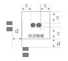
予め定められた段差ルールに基づいて自動設計された段差事例の概略図を示す図2を参照する。図2に示すように、電子部品のステンシル開口に一対一で対応する予め定められた段差ルールが、段差厚の差を0.3とし、電子部品の段差のサイドフレームから段差の内側のステンシル開口までの距離cをeよりも大きくし、電子部品の段差のサイドフレームから段差の外側のステンシル開口までの距離dをfよりも大きくする(e及びfは、対応する予め定められた段差ルールで要求される寸法値である)ことを要求している場合、自動的に開設される段差は、c>e及びd>fを満たす必要があり(c及びdは、段差のサイドフレームから段差の内外の開口までの実際の距離を表す)、2つの条件を同時に満たせない場合には、優先的にc>eを満たすようにする。 Please refer to FIG. 2, which shows a schematic diagram of automatically designed step cases based on predetermined step rules. As shown in FIG. 2, a predetermined step rule with a one-to-one correspondence to the stencil opening of the electronic component is that the step thickness difference is 0.3, and the stencil opening from the side frame of the electronic component step to the inner side of the step. The distance c from the side frame of the electronic component step to the stencil opening outside the step is greater than f (where e and f are the corresponding predetermined step rules are required dimensions), the automatically opened step must satisfy c>e and d>f (where c and d are from the side frame of the step to the represents the actual distance to the inner and outer openings), and if the two conditions cannot be satisfied at the same time, preferentially satisfy c>e.
前記段差領域の段差の中央に段差表記を追加する。前記段差表記には、当該電子部品のステンシル開口における段差厚及び段差面情報が含まれる。 A step notation is added to the center of the step in the step region. The step notation includes step thickness and step surface information in the stencil opening of the electronic component.
例えば、段差の設計が完了した後に、表記ST=0.15を自動で追加する(段差面がスキージ面であり、段差厚が0.15であることを表す)。 For example, after the step design is completed, the notation ST=0.15 is automatically added (indicating that the step surface is the squeegee surface and the step thickness is 0.15).
ステップS19において、段差が設計されたステンシル段差設計ファイルを形成し、形成したステンシル段差設計ファイルが合格か否かをリアルタイム検出する。そして、合格の場合にはステップS10を実行して段差式ステンシルの設計を終了し、開口設計ファイルを出力する。一方、不合格の場合には、ステップS10’を実行し、ステンシル段差設計ファイルを手作業で修正するよう指示するとともに、検査レポートが合格となるまで、ステンシル段差設計ファイルが合格か否かのリアルタイム検出を繰り返す。本実施例では、修正命令を出力すると、オペレータが、手作業による拡張、収縮又は手作業による再設計によって、ステンシル段差設計ファイルが合格するまでステンシル段差設計ファイルを修正し直す。本実施例において、前記合格したステンシル段差設計ファイルは、DXF、ガーバー等のフォーマットの設計ファイルを含んでいる。 In step S19, a stencil step design file in which steps are designed is formed, and whether or not the formed stencil step design file is acceptable is detected in real time. Then, in the case of acceptance, step S10 is executed to finish designing the stepped stencil and output an opening design file. On the other hand, if the stencil step design file fails, step S10′ is executed to instruct manual correction of the stencil step design file, and real-time confirmation of whether the stencil step design file is acceptable until the inspection report is passed. Repeat detection. In this embodiment, outputting the modification instructions causes the operator to modify the stencil step design file again by manual expansion, contraction, or manual redesign until the stencil step design file passes. In this embodiment, the accepted stencil step design files include design files in formats such as DXF, Gerber, and the like.
本実施例は、コンピュータプログラムが記憶されたコンピュータ可読記憶媒体を提供する。当該プログラムは、プロセッサにより実行される際に前記ステンシル段差の設計方法を実現する。 This embodiment provides a computer-readable storage medium having a computer program stored thereon. The program implements the stencil step design method when executed by a processor.
当業者であれば理解可能なように、上記各方法の実施例における全部又は一部のステップは、コンピュータプログラムに関連するハードウエアによって実現可能である。また、上記のコンピュータプログラムは、コンピュータ可読記憶媒体に記憶可能である。当該プログラムを実行する際には、上記各方法の実施例を含むステップが実行される。また、上記の記憶媒体には、ROM、RAM、磁気ディスク又は光ディスク等のプログラムコードを記憶可能な各種媒体が含まれる。 As can be understood by a person skilled in the art, all or part of the steps in the above method embodiments can be implemented by hardware associated with a computer program. Also, the above computer program can be stored in a computer-readable storage medium. When the program is executed, the steps including the embodiment of each method described above are executed. Further, the above storage medium includes various media capable of storing program codes, such as ROM, RAM, magnetic disk, or optical disk.
本実施例における前記ステンシル段差の設計方法は、現在の業界における方法と比較して、90%以上の段差の設計を自動で完了させることができ、且つ、当該設計は加工要求を満たすものである。これにより、工程への人為的介入が省略され、いくつかの簡単なステップで設計を完了させることができる。したがって、60~80%以上の時間を節約可能となり、ステンシル段差の設計ミスの確率も低下する。且つ、本方法は、設計者の技能や知識の把握度合に対する要求が高くないため、一般的なオペレータでも完了させることができる。これにより、該当現場の人員の流動が企業にもたらすリスクを大幅に低下させることができるため、企業の人件費削減の一助とすることができる。 The stencil step design method in this embodiment can automatically complete step design for more than 90% compared with the methods in the current industry, and the design can meet the processing requirements. . This eliminates human intervention in the process and allows the design to be completed in a few simple steps. Therefore, time can be saved by 60 to 80% or more, and the probability of stencil step design errors is reduced. In addition, since this method does not require a high level of skill or knowledge of the designer, it can be completed by a general operator. As a result, it is possible to greatly reduce the risk posed to the company by the movement of personnel at the relevant site, and it is possible to help reduce the personnel cost of the company.
[実施例2]
本実施例は、ステンシル段差の設計システムを提供する。当該設計システムは、回路基板における電子部品のステンシル開口データを取得する取得モジュールと、電子部品のステンシル開口を1つずつ識別して、段差の作製が必要か否かを判断し、段差の作製が必要な場合には、電子部品のステンシル開口に一対一で対応する予め定められた段差ルールに基づき、段差の作製が必要なステンシル開口について段差を設計するとともに、段差が設計されたステンシル段差設計ファイルを形成し、出力モジュールを通じて当該ステンシル段差設計ファイルを出力する一方、段差の作製が不要な場合には、段差式ステンシルの設計を終了し、前記出力モジュールを通じて開口設計ファイルを出力する処理モジュールと、を含んでいる。[Example 2]
This embodiment provides a stencil step design system. The design system includes an acquisition module that acquires stencil opening data of electronic components on a circuit board, and identifies stencil openings of electronic components one by one, determines whether or not steps need to be created, and determines whether steps need to be created. If necessary, a stencil step design file in which steps are designed, along with step designs for stencil openings that need to be made, based on predetermined step rules that correspond one-to-one with electronic component stencil openings. and outputting the stencil stepped design file through an output module, while completing the design of the stepped stencil and outputting an opening design file through the output module when fabrication of steps is not required; contains.
以下に、図面を組み合わせて、本実施例で提供するステンシル段差の設計システムについて詳細に述べる。ここで、ステンシル段差の設計システムの一実施例における原理構造の概略図を示す図3を参照する。図3に示すように、前記ステンシル段差の設計システム3は、読取モジュール31、処理モジュール32、取得モジュール33及び出力モジュール34を含んでいる。 The stencil step design system provided in this embodiment will be described in detail below in combination with the drawings. Reference is now made to FIG. 3, which shows a schematic diagram of the principle structure in one embodiment of the stencil step design system. As shown in FIG. 3 , the stencil
前記読取モジュール31は、回路基板のCADファイルを読み取り、回路基板のCADファイルをCADグラフィックデータに変換して保存する。そして、CADファイル内のパッケージ情報及び関連の開口属性情報を対応するCAD部品層にロードする。本実施例では、CADファイル内のパッケージ情報及び関連の開口属性情報を対応するCAD部品層にロードするため、段差を自動的に開設する際に、どの開口が1つのパッケージに属しているのかを明確に知ることができる。 The
前記読取モジュール31に連結される処理モジュール32は、CADグラフィックデータに対応するステンシル開口ガーバーデータが存在するか否かを判断し、存在する場合には、ステンシル開口ガーバーデータと前記CADグラフィックデータについて座標位置の較正を行う(実施例では、「処理モジュール32が座標位置の較正を行う」とは、ステンシル開口ガーバーデータと前記CADグラフィックデータを整列させることをいう)。そして、CAD部品層における関連の開口属性情報をステンシル開口ガーバーデータにおける対応するステンシル開口に追加することによってステンシル開口層を生成し、前記取得モジュール33を呼び出す。一方、ステンシル開口ガーバーデータが存在しない場合には、CADグラフィックデータから変換対象のステンシル開口はんだペースト層を抽出し、ステンシル開口層を生成して、前記取得モジュール33を呼び出す。 A
前記読取モジュール31及び処理モジュール32に連結される取得モジュール33は、前記回路基板における電子部品のステンシル開口データを取得する。本実施例において、回路基板における電子部品のステンシル開口データには、電子部品の座標、電子部品のパッケージ、電子部品の部品コード等が含まれている。 An
前記処理モジュール32は、ステンシル開口データを記憶するステンシル開口データベースが予め構築されているか否かを検索し、構築されている場合には、ステンシル開口データベースにおいて、電子部品のステンシル開口の段差厚属性を自動でマッチングする。一方、構築されていない場合には、ステンシル開口データのうち段差の作製が必要なステンシル開口に段差厚属性を追加する。 The
前記処理モジュール32は、更に、電子部品のステンシル開口を1つずつ識別して、段差の作製が必要か否かを判断する。そして、段差の作製が必要な場合には、電子部品のステンシル開口に一対一で対応する予め定められた段差ルールに基づき、段差の作製が必要なステンシル開口について段差を設計するとともに、段差が設計されたステンシル段差設計ファイルを形成する。一方、段差の作製が不要な場合には、段差が設計されたステンシル段差設計ファイルを形成する。また、形成したステンシル段差設計ファイルが合格か否かをリアルタイム検出し、合格の場合には、前記出力モジュール34を呼び出して、前記ステンシル段差設計ファイルを出力する。一方、不合格の場合には、ステンシル段差設計ファイルを手作業で修正するよう指示するとともに、検査レポートが合格となるまで、ステンシル段差設計ファイルが合格か否かのリアルタイム検出を繰り返す。そして、前記出力モジュール34を呼び出して、合格したステンシル段差設計ファイルを出力する。 The
前記処理モジュール32は、具体的に、前記段差厚属性に基づいて、即ち、前記予め定められたステンシルベース厚みに基づいて、電子部品のステンシル開口の予め定められたステンシルベース厚みを検索する。そして、予め定められたステンシルベース厚みに基づき、電子部品のステンシル開口の段差厚値が前記予め定められたステンシルベース厚みと等しいか否かを判断し、等しい場合には、電子部品のステンシル開口に段差の作製は不要であると識別する。一方、等しくない場合には、電子部品のステンシル開口に段差の作製が必要であると識別する。 The
本実施例において、上記の電子部品のステンシル開口に一対一で対応する予め定められた段差ルールには、電子部品のステンシル開口における段差厚の差が予め定められた厚み差の閾値であること、電子部品の段差のサイドフレームから内側のステンシル開口までの距離が第1の予め定められた距離の範囲に位置すること、及び/又は、電子部品の段差のサイドフレームから外側のステンシル開口までの距離が第2の予め定められた距離の範囲に位置すること、が含まれている。 In the present embodiment, the predetermined step rule corresponding to the stencil opening of the electronic component on a one-to-one basis includes that the step thickness difference in the stencil opening of the electronic component is a predetermined thickness difference threshold; The distance from the side frame of the step of the electronic component to the inner stencil opening is within a first predetermined distance range and/or the distance from the side frame of the step of the electronic component to the outer stencil opening. is located within a second predetermined distance range.
説明すべき点として、上記設計システムにおける各モジュールの区分は論理機能の区分にすぎず、実際に実現する際には、全部又は一部を1つの物理的実体に集積してもよく、あるいは、物理的に切り離してもよい。且つ、これらのモジュールは、全てを処理デバイスによりソフトウエアを呼び出す形式で実現してもよく、全てをハードウエア形式で実現してもよく、あるいは、一部のモジュールを処理デバイスによりソフトウエアを呼び出す形式で実現し、且つ一部のモジュールをハードウエア形式で実現してもよい。例えば、xモジュールは、単独で設けられた処理デバイスとしてもよく、あるいは、上記設計システムのいずれかのチップに集積して実現してもよい。また、xモジュールは、プログラムコード形式で上記設計システムのメモリに記憶され、上記設計システムのいずれかの処理デバイスによって上記xモジュールの機能を呼び出して実行してもよい。その他のモジュールの実現についてもこれと同様である。これらのモジュールは、全部又は一部を一体的に集積してもよく、あるいは、個別に実現してもよい。また、ここで記載する処理デバイスは、信号処理能力を有する集積回路とすることができる。実現過程において、上記方法の各ステップ又は上記の各モジュールは、プロセッサ部材におけるハードウエアの集積論理回路又はソフトウエア形式の命令により完成可能である。上述したモジュールは、上記方法を実施する1又は複数の集積回路として配置可能である。例えば、1又は複数の特定用途向け集積回路(Application Specific Integrated Circuit,ASICと略称)、1又は複数のマイクロプロセッサ(Digital Singnal Processor,DSPと略称)、1又は複数のフィールドプログラマブルゲートアレイ(Field Programmable Gate Array,FPGAと略称)等として配置可能である。上記いずれかのモジュールが、処理デバイスによりプログラムコードを呼び出すことによって実現される場合、当該処理デバイスは、中央処理装置(Central Processing Unit,CPUと略称)のような汎用プロセッサや、プログラムコードを呼び出し可能なその他のプロセッサとすることができる。これらのモジュールは、一体的に集積することにより、システムオンチップ(System-on-a-chip,SOCと略称)の形式で実現可能である。 It should be noted that the division of each module in the above design system is merely a division of logical functions, and in actual implementation may be integrated in whole or in part into one physical entity, or They can be physically separated. These modules may all be implemented in a form in which software is called by a processing device, all may be implemented in a form of hardware, or some modules may be implemented in a form in which software is called by a processing device. format, and some modules may be implemented in hardware format. For example, the x-module may be a stand-alone processing device, or may be integrated into a chip in any of the design systems described above. The x-modules may also be stored in the memory of the design system in program code form and the functions of the x-modules may be invoked and executed by any processing device of the design system. Realization of other modules is similar to this. These modules may be integrally integrated in whole or in part, or may be realized separately. Also, the processing devices described herein may be integrated circuits having signal processing capabilities. In the process of implementation, the steps of the above method or each of the above modules can be accomplished by hardware integrated logic circuits or software instructions in a processor component. The modules described above may be arranged as one or more integrated circuits implementing the methods described above. For example, one or more Application Specific Integrated Circuits (abbreviated as ASIC), one or more microprocessors (Digital Signal Processor, abbreviated as DSP), one or more field programmable gate arrays (Field Programmable Gate Array, abbreviated as FPGA) or the like. When any of the above modules is realized by calling program code by a processing device, the processing device can call the program code or a general-purpose processor such as a central processing unit (abbreviated as CPU). can be any other processor. These modules can be realized in the form of a system-on-a-chip (abbreviated as SOC) by integrally integrating them.
[実施例3]
本実施例は、デバイスを提供する。ここで、デバイスの一実施例における原理構造の概略図を示す図4を参照する。図4に示すように、前記デバイス4は、プロセッサ41、メモリ42、送受信装置43、通信インターフェース44又は/及び通信バス45を含んでいる。メモリ42及び通信インターフェース44は、通信バス45を介してプロセッサ41及び送受信装置43に接続されており、相互の通信を可能とする。メモリ42は、コンピュータプログラムを記憶するために用いられ、通信インターフェース44はその他のデバイスとの通信に用いられる。また、プロセッサ43と送受信装置43は、コンピュータプログラムを実行し、デバイス4に上述したステンシル段差の設計方法における各ステップを実行させるために用いられる。[Example 3]
This embodiment provides a device. Reference is now made to FIG. 4, which shows a schematic diagram of the principle structure in one embodiment of the device. As shown in FIG. 4, the
上記で言及した通信バスは、ペリフェラルコンポーネントインターコネクト(Peripheral Component Interconnect,PCIと略称)バス、又はイーアイサ(Extended Industry Standard Architecture,EISAと略称)バス等とすることができる。また、当該通信バスは、アドレスバス、データバス、制御バス等に分けられる。なお、図示の都合上、図中では1本の太線のみを用いて示しているが、1本のバス又は1種類のバスしか存在しないことを意味するものではない。通信インターフェースは、データベースアクセス装置とその他のデバイス(例えば、クライアント、リーダ/ライタライブラリ及び読取専用ライブラリ)との通信を実現するために用いられる。また、メモリは、ランダムアクセスメモリ(Random Access Memory,RAMと略称)を含むこともあれば、不揮発性メモリ(non-volatile memory)を含む場合もあり、例えば少なくとも1つの磁気ディスクメモリを含んでいる。 The communication bus referred to above may be a Peripheral Component Interconnect (PCI) bus or an Extended Industry Standard Architecture (EISA) bus or the like. Also, the communication bus is divided into an address bus, a data bus, a control bus, and the like. For convenience of illustration, only one thick line is used in the drawing, but this does not mean that there is only one bus or one type of bus. A communication interface is used to implement communication between the database access device and other devices (eg, clients, reader/writer libraries and read-only libraries). The memory may also include random access memory (abbreviated as RAM) or may include non-volatile memory, such as at least one magnetic disk memory. .
前記プロセッサは、中央処理装置(Central Processing Unit,CPUと略称)、ネットワークプロセッサ(Network Processor,NPと略称)等を含む汎用プロセッサとしてもよく、デジタルシグナルプロセッサ(Digital Signal Processing,DSPと略称)、特定用途向け集積回路(Application Specific Integrated Circuit,ASICと略称)、フィールドプログラマブルゲートアレイ(Field Programmable Gate Array,FPGAと略称)、又は、その他のプログラマブルロジックデバイス、ディスクリートゲート、又はトランジスター論理デバイス、ディスクリートハードウエアアセンブリとしてもよい。 The processor may be a general-purpose processor including a central processing unit (abbreviated as CPU), a network processor (abbreviated as NP), a digital signal processor (abbreviated as DSP), a specific Application Specific Integrated Circuit (ASIC), Field Programmable Gate Array (FPGA) or other programmable logic device, discrete gate or transistor logic device, discrete hardware assembly may be
本発明で記載するステンシル段差の設計方法の保護範囲は、本実施例で列挙したステップの実行順に限らず、本発明の原理に基づき実施される従来技術のステップの増減やステップの置き換えよって実現される方法は、いずれも本発明の保護範囲に含まれる。 The scope of protection of the stencil step design method described in the present invention is not limited to the order of execution of the steps enumerated in the present embodiment, but can be realized by increasing, decreasing, or replacing steps in the prior art based on the principles of the present invention. Any method is included in the protection scope of the present invention.
本発明は、更に、ステンシル段差の設計システムを提供する。前記ステンシル段差の設計システムは、本発明で記載するステンシル段差の設計方法を実現可能である。しかし、本発明で記載するステンシル段差の設計方法を実現する装置は、本実施例で列挙したステンシル段差の設計システムの構造を含むがこれに限らず、本発明の原理に基づき実施される従来技術の構造の変更及び置き換えは、いずれも本発明の保護範囲に含まれる。 The present invention further provides a stencil step design system. The stencil step design system can implement the stencil step design method described in the present invention. However, the apparatus for implementing the stencil step design method described in the present invention includes, but is not limited to, the structure of the stencil step design system enumerated in this embodiment, and the prior art implemented based on the principles of the present invention. Any structural modification and replacement of is included in the protection scope of the present invention.
以上述べたように、本発明で記載するステンシル段差の設計方法、システム、コンピュータ可読記憶媒体及びデバイスは、現在の業界における方法と比較して、90%以上の段差の設計を自動で完了させることができ、且つ、当該設計は加工要求を満たすものである。これにより、工程への人為的介入が省略され、いくつかの簡単なステップで設計を完了させることができる。したがって、60~80%以上の時間を節約可能となり、ステンシル段差の設計ミスの確率が低下する。且つ、本発明は、設計者の技能や知識の把握度合に対する要求が高くないため、一般的なオペレータでも完了させることができる。これにより、該当現場の人員の流動が企業にもたらすリスクを大幅に低下させられることができるため、企業の人件費削減の一助とすることができる。本発明は、従来技術における様々な欠点を効果的に解消するものであり、高度な産業上の利用価値を有する。 As described above, the stencil step design method, system, computer-readable storage medium, and device described in the present invention can automatically complete 90% or more step designs compared to current industry methods. and the design meets processing requirements. This eliminates human intervention in the process and allows the design to be completed in a few simple steps. Therefore, 60-80% or more of time can be saved, and the probability of stencil step design errors is reduced. Moreover, since the present invention does not require a high level of skill or knowledge of the designer, even a general operator can complete the process. As a result, it is possible to greatly reduce the risk that the movement of personnel at the site poses to the company, which can help reduce the personnel cost of the company. INDUSTRIAL APPLICABILITY The present invention effectively solves various drawbacks in the prior art and has high industrial utility value.
上記の実施例は本発明の原理と効果を例示的に説明するものにすぎず、本発明を制限するものではない。本技術を熟知する者であれば、本発明の精神及び範疇を逸脱しないことを前提に、上記の実施例を補足又は変形することが可能である。従って、当業者が本発明で開示する精神及び技術思想を逸脱することなく完了するあらゆる等価の補足又は変形は、依然として本発明の特許請求の範囲に含まれる。 The above embodiments are merely illustrative of the principles and effects of the present invention, and are not intended to limit the present invention. Those skilled in the art can supplement or modify the above-described embodiments without departing from the spirit and scope of the present invention. Therefore, any equivalent supplements or modifications completed by a person skilled in the art without departing from the spirit and concept disclosed in the present invention are still included in the scope of the claims of the present invention.
3 ステンシル段差の設計システム
31 読取モジュール
32 処理モジュール
33 取得モジュール
34 出力モジュール
4 デバイス
41 プロセッサ
42 メモリ
43 送受信装置
44 通信インターフェース
45 通信バス
S11~S10 ステップ
3 Stencil
Claims (10)
Translated fromJapanese処理モジュールが、電子部品のステンシル開口を1つずつ識別して、段差の作製が必要か否かを判断し、
前記段差の作製が必要な場合には、前記電子部品のステンシル開口に一対一で対応する予め定められた段差ルールに基づき、段差の作製が必要なステンシル開口について段差を設計するとともに、段差が設計されたステンシル段差設計ファイルを形成し、出力モジュールを通じて当該ステンシル段差設計ファイルを出力する一方、前記段差の作製が不要な場合には、段差式ステンシルの設計を終了し、開口設計ファイルを出力すること、を含むことを特徴とするステンシル段差の設計方法。an acquisition module for acquiring stencil opening data of electronic components on a circuit board;
a processing module identifying, one by one, stencil openings in the electronic component to determine if step fabrication is required;
When it is necessary to createthe steps, the steps are designed for the stencil openings that need to be created based on predetermined step rules corresponding to the stencil openings ofthe electronic component one-to-one, and the steps are designed. and outputting the stencil step design filethrough an output module. Ifthe steps need not be created, the design of the step stencil is finished and the opening design file is output. A method for designing a stencil step, comprising:
読取モジュールが、前記回路基板のCADファイルを読み取り、前記回路基板のCADファイルをCADグラフィックデータに変換して保存するとともに、前記回路基板のCADファイル内のパッケージ情報及び関連の開口属性情報を対応するCAD部品層にロードし、
前記処理モジュールが、前記CADグラフィックデータに対応するステンシル開口ガーバーデータが存在するか否かを判断し、存在する場合には、前記ステンシル開口ガーバーデータと前記CADグラフィックデータについて座標位置の較正を行った後に、前記CAD部品層における前記関連の開口属性情報を前記ステンシル開口ガーバーデータにおける対応するステンシル開口に追加することによってステンシル開口層を生成する一方、前記ステンシル開口ガーバーデータが存在しない場合には、前記CADグラフィックデータから変換対象のステンシル開口はんだペースト層を抽出し、対応するステンシル開口層を生成すること、を更に含むことを特徴とする請求項1に記載のステンシル段差の設計方法。Before obtaining stencil aperture data for electronic components onthe circuit board,
Areading module reads the CAD file ofthe circuit board, converts the CAD file of the circuit board into CAD graphic data for storage, and corresponds package information and related opening attribute information in the CAD file of thecircuit board. load into the CAD part layer,
Theprocessing module determined whether stencil opening Gerber data corresponding to the CAD graphic data existed, and if so, calibrated coordinate positions forthe stencil opening Gerber data and the CAD graphic data. Later, generating a stencil opening layer by addingthe associated opening attribute information inthe CAD part layer to corresponding stencil openings inthe stencil opening Gerber data, while ifthe stencil opening Gerber data does not exist,the 2. The stencil step design method of claim 1, further comprising extracting a stencil opening solder paste layer to be converted from CAD graphic data and generating a corresponding stencil opening layer.
前記処理モジュールが、前記電子部品のステンシル開口データを記憶するステンシル開口データベースが予め構築されているか否かを検索し、構築されている場合には、前記ステンシル開口データベースにおいて、前記電子部品のステンシル開口の段差厚属性を自動でマッチングする一方、構築されていない場合には、前記ステンシル開口データのうち段差の作製が必要なステンシル開口に前記電子部品のステンシル開口の段差厚属性を追加すること、を更に含むことを特徴とする請求項2に記載のステンシル段差の設計方法。After obtaining stencil aperture data for electronic components onthe circuit board,
The processing module searches whether or not a stencil opening database storing stencil opening data of the electronic componenthasbeen constructed in advance. while automatically matching the step thickness attribute of the electronic component, if not constructed, addingthe step thickness attribute of the stencil opening of the electronic component to the stencil opening that needs to be created inthe stencil opening data. 3. The method of designing a stencil step as recited in claim 2, further comprising:
前記処理モジュールが、前記段差厚属性に基づいて、前記電子部品のステンシル開口の予め定められたステンシルベース厚みを検索し、
前記予め定められたステンシルベース厚みに基づき、前記電子部品のステンシル開口の段差厚値が前記予め定められたステンシルベース厚みと等しいか否かを判断し、等しい場合には、前記電子部品のステンシル開口に段差の作製は不要であると識別する一方、等しくない場合には、前記電子部品のステンシル開口に段差の作製が必要であると識別すること、を含むことを特徴とする請求項3に記載のステンシル段差の設計方法。The step of identifying one by one the stencil openings of the electronic component and determining whether it is necessary to createa step ,
said processing module retrieving a predetermined stencil base thickness of a stencil opening ofsaid electronic component based on said step thickness attribute;
Based onthe predetermined stencil base thickness, it is determined whether a step thickness value of the stencil opening ofthe electronic component is equal to the predetermined stencil base thickness, and if equal, the stencil opening ofthe electronic component is determined.4. The method of claim 3, further comprising: identifying that step fabrication is not required for the stencil opening of the electronic component while identifying that step fabrication is not required for the stencil opening of the electronic component if not equal. stencil step design method.
前記電子部品のステンシル開口における段差厚の差が予め定められた厚み差の閾値であること、
前記電子部品の段差のサイドフレームから内側のステンシル開口までの距離が第1の予め定められた距離の範囲に位置すること、及び/又は、
前記電子部品の段差のサイドフレームから外側のステンシル開口までの距離が第2の予め定められた距離の範囲に位置すること、が含まれることを特徴とする請求項4に記載のステンシル段差の設計方法。The predetermined step rule corresponding to the stencil opening of the electronic component on a one-to-one basis includes:
The step thickness difference in the stencil opening of the electronic component is a predetermined thickness difference threshold;
the distance from the side frame of the step of the electronic component to the inner stencil opening is within a first predetermined distance range; and/or
5. The stencil step design of claim 4, including a distance from the side frame of the electronic component step to the outer stencil opening being within a second predetermined distance range. Method.
前記処理モジュールが、前記第1の予め定められた距離の範囲及び/又は前記第2の予め定められた距離の範囲に基づいて、前記電子部品のステンシル開口の段差領域を算出し、
前記段差領域の段差の中央に、前記電子部品のステンシル開口における段差厚及び段差面情報が含まれる段差表記を追加すること、を含むことを特徴とする請求項5に記載のステンシル段差の設計方法。The step of designinga step for a stencil opening that needs to be created based on the predetermined step rule includes:
wherein the processing module calculates a stepped area of a stencil opening ofthe electronic component based on the first predetermined range of distances and/or the second predetermined range of distances;
6. The method of designing a stencil step according to claim 5, further comprising adding a step notation including step thickness and step surface information in the stencil opening ofthe electronic component to the center of the step of the step area. .
前記処理モジュールが、形成した前記ステンシル段差設計ファイルが合格か否かをリアルタイム検出し、合格の場合には、前記出力モジュールが、前記ステンシル段差設計ファイルを出力し、不合格の場合には当該ステンシル段差設計ファイルに対する修正命令を出力すること、を更に含むことを特徴とする請求項6に記載のステンシル段差の設計方法。After forming a stencil step design file in whichthe steps are designed,
Theprocessing module detects in real time whether theformed stencil step design file is acceptable, the output module outputs the stencil step design file if it is acceptable, and the stencil step design file if it is unacceptable. 7. The method of designing a stencil step according to claim 6, further comprising outputting modification instructions for the step design file.
前記電子部品のステンシル開口を1つずつ識別して、段差の作製が必要か否かを判断し、前記段差の作製が必要な場合には、前記電子部品のステンシル開口に一対一で対応する予め定められた段差ルールに基づき、前記段差の作製が必要なステンシル開口について前記段差を設計するとともに、前記段差が設計されたステンシル段差設計ファイルを形成し、出力モジュールを通じて当該ステンシル段差設計ファイルを出力する一方、前記段差の作製が不要な場合には、段差式ステンシルの設計を終了し、前記出力モジュールを通じて開口設計ファイルを出力する処理モジュールと、を含むことを特徴とするステンシル段差の設計システム。an acquisition module for acquiring stencil aperture data for electronic components on a circuit board;
The stencil openings ofthe electronic component are identified one by one, and it isdetermined whether or not steps need to be produced. designing the steps forthe stencil openings required to producethe steps according to the determined step rules, forming a stencil step design file in whichthe steps are designed, and outputting the stencil step design file through an output module; On the other hand, a stencil step design system,comprising : a processing module that finishes designing the step type stencil and outputs an opening design file through the output module when the steps need not be produced.
当該プログラムは、プロセッサにより実行される際に、請求項1乃至請求項7のいずれか1項に記載のステンシル段差の設計方法を実現することを特徴とするコンピュータ可読記憶媒体。A computer-readable storage medium storing a computer program,
A computer-readable storage medium, wherein the program implements the stencil step design method according to any one of claims 1 to 7 when executed by a processor.
前記メモリはコンピュータプログラムを記憶するために用いられ、前記プロセッサは、前記メモリに記憶されているコンピュータプログラムを実行することにより、デバイスに請求項1乃至請求項7のいずれか1項に記載のステンシル段差の設計方法を実行させるために用いられることを特徴とするデバイス。including a processor and memory;
8. The memory is used for storing a computer program, and the processor executes the computer program stored in the memory to causethe device to perform the processing according to any one of claims 1 to 7. A device used to implement a stencil step design method.
Applications Claiming Priority (3)
| Application Number | Priority Date | Filing Date | Title |
|---|---|---|---|
| CN201910209598.8ACN109977518B (en) | 2019-03-19 | 2019-03-19 | Method and system for designing web stair, computer readable storage medium and equipment |
| CN201910209598.8 | 2019-03-19 | ||
| PCT/CN2019/126332WO2020186850A1 (en) | 2019-03-19 | 2019-12-18 | Mesh plate steps design method, system, computer readable storage medium and device |
Publications (2)
| Publication Number | Publication Date |
|---|---|
| JP2022524877A JP2022524877A (en) | 2022-05-10 |
| JP7202557B2true JP7202557B2 (en) | 2023-01-12 |
Family
ID=67079506
Family Applications (1)
| Application Number | Title | Priority Date | Filing Date |
|---|---|---|---|
| JP2021555522AActiveJP7202557B2 (en) | 2019-03-19 | 2019-12-18 | Stencil step design method, system, computer readable storage medium and device |
Country Status (5)
| Country | Link |
|---|---|
| US (1) | US12073164B2 (en) |
| EP (1) | EP3923153A4 (en) |
| JP (1) | JP7202557B2 (en) |
| CN (1) | CN109977518B (en) |
| WO (1) | WO2020186850A1 (en) |
Families Citing this family (6)
| Publication number | Priority date | Publication date | Assignee | Title |
|---|---|---|---|---|
| CN109977518B (en)* | 2019-03-19 | 2021-02-12 | 上海望友信息科技有限公司 | Method and system for designing web stair, computer readable storage medium and equipment |
| CN112232014B (en)* | 2020-09-16 | 2022-07-29 | 上海望友信息科技有限公司 | Steel mesh avoiding design method, design device, electronic equipment and storage medium |
| CN112579532B (en)* | 2020-12-18 | 2023-07-28 | 德中(天津)技术发展股份有限公司 | Automatic steel mesh opening library building method and system |
| CN113573477B (en)* | 2021-06-21 | 2022-06-03 | 广州添利电子科技有限公司 | PCB (printed Circuit Board) manufacturing indication method, production coefficient generation method, pre-expansion system, medium and equipment |
| CN115408975B (en)* | 2022-09-21 | 2025-08-12 | 上海望友信息科技有限公司 | Method, system, electronic equipment and storage medium for micro-modified steel mesh design |
| CN118862815B (en)* | 2023-04-18 | 2025-05-27 | 北京平头哥信息技术有限公司 | Method, system and storage medium for detecting manufacturability of chip carrier |
Citations (2)
| Publication number | Priority date | Publication date | Assignee | Title |
|---|---|---|---|---|
| US20040089413A1 (en) | 2002-08-08 | 2004-05-13 | Michael Murphy | System and method for modifying electronic design data |
| JP2016112864A (en) | 2014-12-18 | 2016-06-23 | 富士通株式会社 | Metal mask data output device and output method |
Family Cites Families (10)
| Publication number | Priority date | Publication date | Assignee | Title |
|---|---|---|---|---|
| JP3044905B2 (en)* | 1992-03-31 | 2000-05-22 | 松下電器産業株式会社 | Design method of opening of metal mask |
| US6321591B1 (en)* | 1999-02-22 | 2001-11-27 | Electronic Controls Design, Inc. | Method and apparatus for measuring spray from a liquid dispensing system |
| CN101452497A (en)* | 2007-12-05 | 2009-06-10 | 英业达股份有限公司 | Method for automatically installing slot element and computer readable storage medium |
| CN102291947B (en)* | 2011-07-29 | 2013-01-30 | 杭州华三通信技术有限公司 | Method for manufacturing through hole pad on step structure of printed circuit board (PCB) and PCB |
| US11176635B2 (en)* | 2013-01-25 | 2021-11-16 | Cyberoptics Corporation | Automatic programming of solder paste inspection system |
| CN108629103B (en)* | 2015-04-08 | 2022-02-11 | 上海望友信息科技有限公司 | SMT patch manufacturing and SMT screen plate manufacturing method and system |
| CN105260569A (en)* | 2015-11-09 | 2016-01-20 | 浪潮集团有限公司 | Method of automatically punching ground holes based on CadenceAllegro |
| CN106227946B (en)* | 2016-07-26 | 2019-03-12 | 上海望友信息科技有限公司 | A kind of PCB web plate production method and system |
| CN106649219B (en)* | 2016-11-21 | 2019-05-24 | 中国空间技术研究院 | A kind of telecommunication satellite design document automatic generation method |
| CN109977518B (en)* | 2019-03-19 | 2021-02-12 | 上海望友信息科技有限公司 | Method and system for designing web stair, computer readable storage medium and equipment |
- 2019
- 2019-03-19CNCN201910209598.8Apatent/CN109977518B/enactiveActive
- 2019-12-18JPJP2021555522Apatent/JP7202557B2/enactiveActive
- 2019-12-18EPEP19920274.8Apatent/EP3923153A4/enactivePending
- 2019-12-18WOPCT/CN2019/126332patent/WO2020186850A1/ennot_activeCeased
- 2019-12-18USUS17/438,895patent/US12073164B2/enactiveActive
Patent Citations (2)
| Publication number | Priority date | Publication date | Assignee | Title |
|---|---|---|---|---|
| US20040089413A1 (en) | 2002-08-08 | 2004-05-13 | Michael Murphy | System and method for modifying electronic design data |
| JP2016112864A (en) | 2014-12-18 | 2016-06-23 | 富士通株式会社 | Metal mask data output device and output method |
Also Published As
| Publication number | Publication date |
|---|---|
| US12073164B2 (en) | 2024-08-27 |
| CN109977518A (en) | 2019-07-05 |
| US20220147684A1 (en) | 2022-05-12 |
| WO2020186850A1 (en) | 2020-09-24 |
| EP3923153A4 (en) | 2022-11-16 |
| CN109977518B (en) | 2021-02-12 |
| EP3923153A1 (en) | 2021-12-15 |
| JP2022524877A (en) | 2022-05-10 |
Similar Documents
| Publication | Publication Date | Title |
|---|---|---|
| JP7202557B2 (en) | Stencil step design method, system, computer readable storage medium and device | |
| JP6754889B2 (en) | Printed circuit board metal mask manufacturing system | |
| US6792593B2 (en) | Pattern correction method, apparatus, and program | |
| EP3951632B1 (en) | System-in-package technology-based process design method and system, medium and device | |
| US11330705B2 (en) | Method, system and apparatus for detecting polarity of component, and computer-readable storage medium | |
| WO2020073631A1 (en) | 3d simulation data generation method and system, and computer storage medium and device | |
| CN113408224A (en) | FPGA layout method for realizing layout legalization by utilizing netlist local re-synthesis | |
| CN111611766A (en) | Method, apparatus and storage medium for determining circuit layout constraints | |
| CN116127908A (en) | Wiring method, device, equipment and storage medium of circuit layout | |
| CN108052771B (en) | Optical reference point recognition method, system, computer-readable storage medium and apparatus | |
| CN111506362B (en) | Processing method, device, storage medium and system for configuration form of game | |
| CN110414123B (en) | Method and equipment for packaging graphic data element based on coordinates | |
| CN114330207B (en) | Chip pad information extraction method, system and electronic device | |
| JPH06274568A (en) | How to expand hierarchical figure data | |
| CN116756082B (en) | Configurable function module file generation method and system | |
| CN116881515B (en) | Method and electronic equipment for comparing capacitance results solved by different algorithms | |
| CN114662443A (en) | Integrated circuit layout design method, device and readable storage medium | |
| CN117648901A (en) | A DRC rule checking method based on Cadence SiP Digital Layout | |
| US10628623B2 (en) | Non-transitory computer-readable recording medium recording detour wiring check program, detour wiring check method, and information processing apparatus | |
| US20060138634A1 (en) | Method for determining the arrangement of contact surfaces on the active upper face of a semiconductor chip | |
| US8762902B2 (en) | System and method for detecting one or more winding paths for patterns on a reticle for the manufacture of semiconductor integrated circuits | |
| CN110781641B (en) | Method for quickly identifying and correcting sensitive graph in layout | |
| CN114140059B (en) | Product management system, method, device and computer-readable storage medium | |
| CN114154938A (en) | Product management system, method, apparatus, and computer-readable storage medium | |
| CN114741992A (en) | Method and device for setting identification, electronic equipment and storage medium |
Legal Events
| Date | Code | Title | Description |
|---|---|---|---|
| A621 | Written request for application examination | Free format text:JAPANESE INTERMEDIATE CODE: A621 Effective date:20210914 | |
| A977 | Report on retrieval | Free format text:JAPANESE INTERMEDIATE CODE: A971007 Effective date:20220907 | |
| A131 | Notification of reasons for refusal | Free format text:JAPANESE INTERMEDIATE CODE: A131 Effective date:20220909 | |
| A521 | Request for written amendment filed | Free format text:JAPANESE INTERMEDIATE CODE: A523 Effective date:20221118 | |
| TRDD | Decision of grant or rejection written | ||
| A01 | Written decision to grant a patent or to grant a registration (utility model) | Free format text:JAPANESE INTERMEDIATE CODE: A01 Effective date:20221129 | |
| A61 | First payment of annual fees (during grant procedure) | Free format text:JAPANESE INTERMEDIATE CODE: A61 Effective date:20221215 | |
| R150 | Certificate of patent or registration of utility model | Ref document number:7202557 Country of ref document:JP Free format text:JAPANESE INTERMEDIATE CODE: R150 |