JP7200880B2 - Film forming method and film forming apparatus - Google Patents
Film forming method and film forming apparatusDownload PDFInfo
- Publication number
- JP7200880B2 JP7200880B2JP2019149953AJP2019149953AJP7200880B2JP 7200880 B2JP7200880 B2JP 7200880B2JP 2019149953 AJP2019149953 AJP 2019149953AJP 2019149953 AJP2019149953 AJP 2019149953AJP 7200880 B2JP7200880 B2JP 7200880B2
- Authority
- JP
- Japan
- Prior art keywords
- film
- gas
- silicon
- nitriding
- plasma
- Prior art date
- Legal status (The legal status is an assumption and is not a legal conclusion. Google has not performed a legal analysis and makes no representation as to the accuracy of the status listed.)
- Active
Links
- 238000000034methodMethods0.000titleclaimsdescription30
- 239000007789gasSubstances0.000claimsdescription207
- 229910052581Si3N4Inorganic materials0.000claimsdescription105
- HQVNEWCFYHHQES-UHFFFAOYSA-Nsilicon nitrideChemical compoundN12[Si]34N5[Si]62N3[Si]51N64HQVNEWCFYHHQES-UHFFFAOYSA-N0.000claimsdescription105
- 230000015572biosynthetic processEffects0.000claimsdescription35
- 238000005121nitridingMethods0.000claimsdescription34
- VYPSYNLAJGMNEJ-UHFFFAOYSA-NSilicium dioxideChemical compoundO=[Si]=OVYPSYNLAJGMNEJ-UHFFFAOYSA-N0.000claimsdescription33
- 229910052710siliconInorganic materials0.000claimsdescription29
- 239000010703siliconSubstances0.000claimsdescription29
- XUIMIQQOPSSXEZ-UHFFFAOYSA-NSiliconChemical compound[Si]XUIMIQQOPSSXEZ-UHFFFAOYSA-N0.000claimsdescription25
- 238000011534incubationMethods0.000claimsdescription25
- 239000000758substrateSubstances0.000claimsdescription20
- 238000012545processingMethods0.000claimsdescription19
- 239000002994raw materialSubstances0.000claimsdescription16
- 230000008569processEffects0.000claimsdescription14
- UFHFLCQGNIYNRP-UHFFFAOYSA-NHydrogenChemical compound[H][H]UFHFLCQGNIYNRP-UHFFFAOYSA-N0.000claimsdescription11
- 239000002184metalSubstances0.000claimsdescription8
- 229910052751metalInorganic materials0.000claimsdescription8
- QGZKDVFQNNGYKY-UHFFFAOYSA-NAmmoniaChemical compoundNQGZKDVFQNNGYKY-UHFFFAOYSA-N0.000claimsdescription5
- 150000004767nitridesChemical class0.000claimsdescription4
- -1silicon halideChemical class0.000claimsdescription4
- 229910052814silicon oxideInorganic materials0.000claimsdescription3
- LXEXBJXDGVGRAR-UHFFFAOYSA-Ntrichloro(trichlorosilyl)silaneChemical groupCl[Si](Cl)(Cl)[Si](Cl)(Cl)ClLXEXBJXDGVGRAR-UHFFFAOYSA-N0.000claimsdescription3
- 239000012528membraneSubstances0.000claimsdescription2
- FDNAPBUWERUEDA-UHFFFAOYSA-Nsilicon tetrachlorideChemical compoundCl[Si](Cl)(Cl)ClFDNAPBUWERUEDA-UHFFFAOYSA-N0.000claimsdescription2
- WFKWXMTUELFFGS-UHFFFAOYSA-NtungstenChemical compound[W]WFKWXMTUELFFGS-UHFFFAOYSA-N0.000claimsdescription2
- 229910052721tungstenInorganic materials0.000claimsdescription2
- 239000010937tungstenSubstances0.000claimsdescription2
- VEXZGXHMUGYJMC-UHFFFAOYSA-MChloride anionChemical compound[Cl-]VEXZGXHMUGYJMC-UHFFFAOYSA-M0.000claims1
- 239000010408filmSubstances0.000description230
- 235000012431wafersNutrition0.000description89
- 229910004298SiO 2Inorganic materials0.000description33
- 238000012360testing methodMethods0.000description31
- 238000011156evaluationMethods0.000description19
- 229910052681coesiteInorganic materials0.000description15
- 229910052906cristobaliteInorganic materials0.000description15
- 239000000377silicon dioxideSubstances0.000description15
- 235000012239silicon dioxideNutrition0.000description15
- 229910052682stishoviteInorganic materials0.000description15
- 229910052905tridymiteInorganic materials0.000description15
- 238000010926purgeMethods0.000description13
- 238000001179sorption measurementMethods0.000description13
- 230000000052comparative effectEffects0.000description11
- 230000002093peripheral effectEffects0.000description9
- 125000004429atomChemical group0.000description6
- 239000000460chlorineSubstances0.000description6
- 230000007246mechanismEffects0.000description6
- 238000012546transferMethods0.000description5
- 238000011282treatmentMethods0.000description5
- XKRFYHLGVUSROY-UHFFFAOYSA-NArgonChemical compound[Ar]XKRFYHLGVUSROY-UHFFFAOYSA-N0.000description4
- MROCJMGDEKINLD-UHFFFAOYSA-NdichlorosilaneChemical compoundCl[SiH2]ClMROCJMGDEKINLD-UHFFFAOYSA-N0.000description4
- 125000004430oxygen atomChemical groupO*0.000description4
- VEXZGXHMUGYJMC-UHFFFAOYSA-NHydrochloric acidChemical compoundClVEXZGXHMUGYJMC-UHFFFAOYSA-N0.000description3
- 238000000231atomic layer depositionMethods0.000description3
- 230000000694effectsEffects0.000description3
- PXHVJJICTQNCMI-UHFFFAOYSA-NnickelSubstances[Ni]PXHVJJICTQNCMI-UHFFFAOYSA-N0.000description3
- 229910052786argonInorganic materials0.000description2
- 230000008859changeEffects0.000description2
- 238000005229chemical vapour depositionMethods0.000description2
- 125000001309chloro groupChemical groupCl*0.000description2
- 238000000151depositionMethods0.000description2
- 230000008021depositionEffects0.000description2
- 238000005516engineering processMethods0.000description2
- 239000001257hydrogenSubstances0.000description2
- 229910052739hydrogenInorganic materials0.000description2
- 238000004519manufacturing processMethods0.000description2
- 230000009467reductionEffects0.000description2
- 239000004065semiconductorSubstances0.000description2
- 239000007787solidSubstances0.000description2
- 239000010936titaniumSubstances0.000description2
- ZCYVEMRRCGMTRW-UHFFFAOYSA-N7553-56-2Chemical compound[I]ZCYVEMRRCGMTRW-UHFFFAOYSA-N0.000description1
- ZAMOUSCENKQFHK-UHFFFAOYSA-NChlorine atomChemical compound[Cl]ZAMOUSCENKQFHK-UHFFFAOYSA-N0.000description1
- RTAQQCXQSZGOHL-UHFFFAOYSA-NTitaniumChemical compound[Ti]RTAQQCXQSZGOHL-UHFFFAOYSA-N0.000description1
- 230000004913activationEffects0.000description1
- 229910021529ammoniaInorganic materials0.000description1
- 238000006243chemical reactionMethods0.000description1
- 229910052801chlorineInorganic materials0.000description1
- 238000010586diagramMethods0.000description1
- 238000007599dischargingMethods0.000description1
- 229910052736halogenInorganic materials0.000description1
- 150000002367halogensChemical class0.000description1
- 239000012535impuritySubstances0.000description1
- 229910052740iodineInorganic materials0.000description1
- 239000011630iodineSubstances0.000description1
- 239000000463materialSubstances0.000description1
- 229910052759nickelInorganic materials0.000description1
- 229910052757nitrogenInorganic materials0.000description1
- 125000004433nitrogen atomChemical groupN*0.000description1
- 229910000069nitrogen hydrideInorganic materials0.000description1
- 238000002203pretreatmentMethods0.000description1
- 238000002407reformingMethods0.000description1
- 150000003376siliconChemical class0.000description1
- 238000003860storageMethods0.000description1
- 239000010409thin filmSubstances0.000description1
- 229910052719titaniumInorganic materials0.000description1
- 230000007723transport mechanismEffects0.000description1
- 238000011144upstream manufacturingMethods0.000description1
Images


Classifications
- C—CHEMISTRY; METALLURGY
- C23—COATING METALLIC MATERIAL; COATING MATERIAL WITH METALLIC MATERIAL; CHEMICAL SURFACE TREATMENT; DIFFUSION TREATMENT OF METALLIC MATERIAL; COATING BY VACUUM EVAPORATION, BY SPUTTERING, BY ION IMPLANTATION OR BY CHEMICAL VAPOUR DEPOSITION, IN GENERAL; INHIBITING CORROSION OF METALLIC MATERIAL OR INCRUSTATION IN GENERAL
- C23C—COATING METALLIC MATERIAL; COATING MATERIAL WITH METALLIC MATERIAL; SURFACE TREATMENT OF METALLIC MATERIAL BY DIFFUSION INTO THE SURFACE, BY CHEMICAL CONVERSION OR SUBSTITUTION; COATING BY VACUUM EVAPORATION, BY SPUTTERING, BY ION IMPLANTATION OR BY CHEMICAL VAPOUR DEPOSITION, IN GENERAL
- C23C16/00—Chemical coating by decomposition of gaseous compounds, without leaving reaction products of surface material in the coating, i.e. chemical vapour deposition [CVD] processes
- C23C16/44—Chemical coating by decomposition of gaseous compounds, without leaving reaction products of surface material in the coating, i.e. chemical vapour deposition [CVD] processes characterised by the method of coating
- C23C16/455—Chemical coating by decomposition of gaseous compounds, without leaving reaction products of surface material in the coating, i.e. chemical vapour deposition [CVD] processes characterised by the method of coating characterised by the method used for introducing gases into reaction chamber or for modifying gas flows in reaction chamber
- C23C16/45523—Pulsed gas flow or change of composition over time
- C23C16/45525—Atomic layer deposition [ALD]
- C—CHEMISTRY; METALLURGY
- C23—COATING METALLIC MATERIAL; COATING MATERIAL WITH METALLIC MATERIAL; CHEMICAL SURFACE TREATMENT; DIFFUSION TREATMENT OF METALLIC MATERIAL; COATING BY VACUUM EVAPORATION, BY SPUTTERING, BY ION IMPLANTATION OR BY CHEMICAL VAPOUR DEPOSITION, IN GENERAL; INHIBITING CORROSION OF METALLIC MATERIAL OR INCRUSTATION IN GENERAL
- C23C—COATING METALLIC MATERIAL; COATING MATERIAL WITH METALLIC MATERIAL; SURFACE TREATMENT OF METALLIC MATERIAL BY DIFFUSION INTO THE SURFACE, BY CHEMICAL CONVERSION OR SUBSTITUTION; COATING BY VACUUM EVAPORATION, BY SPUTTERING, BY ION IMPLANTATION OR BY CHEMICAL VAPOUR DEPOSITION, IN GENERAL
- C23C16/00—Chemical coating by decomposition of gaseous compounds, without leaving reaction products of surface material in the coating, i.e. chemical vapour deposition [CVD] processes
- C23C16/22—Chemical coating by decomposition of gaseous compounds, without leaving reaction products of surface material in the coating, i.e. chemical vapour deposition [CVD] processes characterised by the deposition of inorganic material, other than metallic material
- C23C16/30—Deposition of compounds, mixtures or solid solutions, e.g. borides, carbides, nitrides
- C23C16/34—Nitrides
- C23C16/345—Silicon nitride
- H—ELECTRICITY
- H01—ELECTRIC ELEMENTS
- H01L—SEMICONDUCTOR DEVICES NOT COVERED BY CLASS H10
- H01L21/00—Processes or apparatus adapted for the manufacture or treatment of semiconductor or solid state devices or of parts thereof
- H01L21/02—Manufacture or treatment of semiconductor devices or of parts thereof
- H01L21/02104—Forming layers
- H01L21/02107—Forming insulating materials on a substrate
- H01L21/02225—Forming insulating materials on a substrate characterised by the process for the formation of the insulating layer
- H01L21/0226—Forming insulating materials on a substrate characterised by the process for the formation of the insulating layer formation by a deposition process
- H01L21/02263—Forming insulating materials on a substrate characterised by the process for the formation of the insulating layer formation by a deposition process deposition from the gas or vapour phase
- H01L21/02271—Forming insulating materials on a substrate characterised by the process for the formation of the insulating layer formation by a deposition process deposition from the gas or vapour phase deposition by decomposition or reaction of gaseous or vapour phase compounds, i.e. chemical vapour deposition
- H01L21/0228—Forming insulating materials on a substrate characterised by the process for the formation of the insulating layer formation by a deposition process deposition from the gas or vapour phase deposition by decomposition or reaction of gaseous or vapour phase compounds, i.e. chemical vapour deposition deposition by cyclic CVD, e.g. ALD, ALE, pulsed CVD
- C—CHEMISTRY; METALLURGY
- C23—COATING METALLIC MATERIAL; COATING MATERIAL WITH METALLIC MATERIAL; CHEMICAL SURFACE TREATMENT; DIFFUSION TREATMENT OF METALLIC MATERIAL; COATING BY VACUUM EVAPORATION, BY SPUTTERING, BY ION IMPLANTATION OR BY CHEMICAL VAPOUR DEPOSITION, IN GENERAL; INHIBITING CORROSION OF METALLIC MATERIAL OR INCRUSTATION IN GENERAL
- C23C—COATING METALLIC MATERIAL; COATING MATERIAL WITH METALLIC MATERIAL; SURFACE TREATMENT OF METALLIC MATERIAL BY DIFFUSION INTO THE SURFACE, BY CHEMICAL CONVERSION OR SUBSTITUTION; COATING BY VACUUM EVAPORATION, BY SPUTTERING, BY ION IMPLANTATION OR BY CHEMICAL VAPOUR DEPOSITION, IN GENERAL
- C23C16/00—Chemical coating by decomposition of gaseous compounds, without leaving reaction products of surface material in the coating, i.e. chemical vapour deposition [CVD] processes
- C23C16/02—Pretreatment of the material to be coated
- C23C16/0272—Deposition of sub-layers, e.g. to promote the adhesion of the main coating
- C—CHEMISTRY; METALLURGY
- C23—COATING METALLIC MATERIAL; COATING MATERIAL WITH METALLIC MATERIAL; CHEMICAL SURFACE TREATMENT; DIFFUSION TREATMENT OF METALLIC MATERIAL; COATING BY VACUUM EVAPORATION, BY SPUTTERING, BY ION IMPLANTATION OR BY CHEMICAL VAPOUR DEPOSITION, IN GENERAL; INHIBITING CORROSION OF METALLIC MATERIAL OR INCRUSTATION IN GENERAL
- C23C—COATING METALLIC MATERIAL; COATING MATERIAL WITH METALLIC MATERIAL; SURFACE TREATMENT OF METALLIC MATERIAL BY DIFFUSION INTO THE SURFACE, BY CHEMICAL CONVERSION OR SUBSTITUTION; COATING BY VACUUM EVAPORATION, BY SPUTTERING, BY ION IMPLANTATION OR BY CHEMICAL VAPOUR DEPOSITION, IN GENERAL
- C23C16/00—Chemical coating by decomposition of gaseous compounds, without leaving reaction products of surface material in the coating, i.e. chemical vapour deposition [CVD] processes
- C23C16/22—Chemical coating by decomposition of gaseous compounds, without leaving reaction products of surface material in the coating, i.e. chemical vapour deposition [CVD] processes characterised by the deposition of inorganic material, other than metallic material
- C23C16/24—Deposition of silicon only
- C—CHEMISTRY; METALLURGY
- C23—COATING METALLIC MATERIAL; COATING MATERIAL WITH METALLIC MATERIAL; CHEMICAL SURFACE TREATMENT; DIFFUSION TREATMENT OF METALLIC MATERIAL; COATING BY VACUUM EVAPORATION, BY SPUTTERING, BY ION IMPLANTATION OR BY CHEMICAL VAPOUR DEPOSITION, IN GENERAL; INHIBITING CORROSION OF METALLIC MATERIAL OR INCRUSTATION IN GENERAL
- C23C—COATING METALLIC MATERIAL; COATING MATERIAL WITH METALLIC MATERIAL; SURFACE TREATMENT OF METALLIC MATERIAL BY DIFFUSION INTO THE SURFACE, BY CHEMICAL CONVERSION OR SUBSTITUTION; COATING BY VACUUM EVAPORATION, BY SPUTTERING, BY ION IMPLANTATION OR BY CHEMICAL VAPOUR DEPOSITION, IN GENERAL
- C23C16/00—Chemical coating by decomposition of gaseous compounds, without leaving reaction products of surface material in the coating, i.e. chemical vapour deposition [CVD] processes
- C23C16/44—Chemical coating by decomposition of gaseous compounds, without leaving reaction products of surface material in the coating, i.e. chemical vapour deposition [CVD] processes characterised by the method of coating
- C23C16/455—Chemical coating by decomposition of gaseous compounds, without leaving reaction products of surface material in the coating, i.e. chemical vapour deposition [CVD] processes characterised by the method of coating characterised by the method used for introducing gases into reaction chamber or for modifying gas flows in reaction chamber
- C23C16/45523—Pulsed gas flow or change of composition over time
- C23C16/45525—Atomic layer deposition [ALD]
- C23C16/45527—Atomic layer deposition [ALD] characterized by the ALD cycle, e.g. different flows or temperatures during half-reactions, unusual pulsing sequence, use of precursor mixtures or auxiliary reactants or activations
- C23C16/45536—Use of plasma, radiation or electromagnetic fields
- C23C16/45542—Plasma being used non-continuously during the ALD reactions
- C—CHEMISTRY; METALLURGY
- C23—COATING METALLIC MATERIAL; COATING MATERIAL WITH METALLIC MATERIAL; CHEMICAL SURFACE TREATMENT; DIFFUSION TREATMENT OF METALLIC MATERIAL; COATING BY VACUUM EVAPORATION, BY SPUTTERING, BY ION IMPLANTATION OR BY CHEMICAL VAPOUR DEPOSITION, IN GENERAL; INHIBITING CORROSION OF METALLIC MATERIAL OR INCRUSTATION IN GENERAL
- C23C—COATING METALLIC MATERIAL; COATING MATERIAL WITH METALLIC MATERIAL; SURFACE TREATMENT OF METALLIC MATERIAL BY DIFFUSION INTO THE SURFACE, BY CHEMICAL CONVERSION OR SUBSTITUTION; COATING BY VACUUM EVAPORATION, BY SPUTTERING, BY ION IMPLANTATION OR BY CHEMICAL VAPOUR DEPOSITION, IN GENERAL
- C23C16/00—Chemical coating by decomposition of gaseous compounds, without leaving reaction products of surface material in the coating, i.e. chemical vapour deposition [CVD] processes
- C23C16/44—Chemical coating by decomposition of gaseous compounds, without leaving reaction products of surface material in the coating, i.e. chemical vapour deposition [CVD] processes characterised by the method of coating
- C23C16/455—Chemical coating by decomposition of gaseous compounds, without leaving reaction products of surface material in the coating, i.e. chemical vapour deposition [CVD] processes characterised by the method of coating characterised by the method used for introducing gases into reaction chamber or for modifying gas flows in reaction chamber
- C23C16/45523—Pulsed gas flow or change of composition over time
- C23C16/45525—Atomic layer deposition [ALD]
- C23C16/45544—Atomic layer deposition [ALD] characterized by the apparatus
- C23C16/45548—Atomic layer deposition [ALD] characterized by the apparatus having arrangements for gas injection at different locations of the reactor for each ALD half-reaction
- C23C16/45551—Atomic layer deposition [ALD] characterized by the apparatus having arrangements for gas injection at different locations of the reactor for each ALD half-reaction for relative movement of the substrate and the gas injectors or half-reaction reactor compartments
- C—CHEMISTRY; METALLURGY
- C23—COATING METALLIC MATERIAL; COATING MATERIAL WITH METALLIC MATERIAL; CHEMICAL SURFACE TREATMENT; DIFFUSION TREATMENT OF METALLIC MATERIAL; COATING BY VACUUM EVAPORATION, BY SPUTTERING, BY ION IMPLANTATION OR BY CHEMICAL VAPOUR DEPOSITION, IN GENERAL; INHIBITING CORROSION OF METALLIC MATERIAL OR INCRUSTATION IN GENERAL
- C23C—COATING METALLIC MATERIAL; COATING MATERIAL WITH METALLIC MATERIAL; SURFACE TREATMENT OF METALLIC MATERIAL BY DIFFUSION INTO THE SURFACE, BY CHEMICAL CONVERSION OR SUBSTITUTION; COATING BY VACUUM EVAPORATION, BY SPUTTERING, BY ION IMPLANTATION OR BY CHEMICAL VAPOUR DEPOSITION, IN GENERAL
- C23C16/00—Chemical coating by decomposition of gaseous compounds, without leaving reaction products of surface material in the coating, i.e. chemical vapour deposition [CVD] processes
- C23C16/44—Chemical coating by decomposition of gaseous compounds, without leaving reaction products of surface material in the coating, i.e. chemical vapour deposition [CVD] processes characterised by the method of coating
- C23C16/455—Chemical coating by decomposition of gaseous compounds, without leaving reaction products of surface material in the coating, i.e. chemical vapour deposition [CVD] processes characterised by the method of coating characterised by the method used for introducing gases into reaction chamber or for modifying gas flows in reaction chamber
- C23C16/45523—Pulsed gas flow or change of composition over time
- C23C16/45525—Atomic layer deposition [ALD]
- C23C16/45553—Atomic layer deposition [ALD] characterized by the use of precursors specially adapted for ALD
- C—CHEMISTRY; METALLURGY
- C23—COATING METALLIC MATERIAL; COATING MATERIAL WITH METALLIC MATERIAL; CHEMICAL SURFACE TREATMENT; DIFFUSION TREATMENT OF METALLIC MATERIAL; COATING BY VACUUM EVAPORATION, BY SPUTTERING, BY ION IMPLANTATION OR BY CHEMICAL VAPOUR DEPOSITION, IN GENERAL; INHIBITING CORROSION OF METALLIC MATERIAL OR INCRUSTATION IN GENERAL
- C23C—COATING METALLIC MATERIAL; COATING MATERIAL WITH METALLIC MATERIAL; SURFACE TREATMENT OF METALLIC MATERIAL BY DIFFUSION INTO THE SURFACE, BY CHEMICAL CONVERSION OR SUBSTITUTION; COATING BY VACUUM EVAPORATION, BY SPUTTERING, BY ION IMPLANTATION OR BY CHEMICAL VAPOUR DEPOSITION, IN GENERAL
- C23C16/00—Chemical coating by decomposition of gaseous compounds, without leaving reaction products of surface material in the coating, i.e. chemical vapour deposition [CVD] processes
- C23C16/44—Chemical coating by decomposition of gaseous compounds, without leaving reaction products of surface material in the coating, i.e. chemical vapour deposition [CVD] processes characterised by the method of coating
- C23C16/458—Chemical coating by decomposition of gaseous compounds, without leaving reaction products of surface material in the coating, i.e. chemical vapour deposition [CVD] processes characterised by the method of coating characterised by the method used for supporting substrates in the reaction chamber
- C23C16/4581—Chemical coating by decomposition of gaseous compounds, without leaving reaction products of surface material in the coating, i.e. chemical vapour deposition [CVD] processes characterised by the method of coating characterised by the method used for supporting substrates in the reaction chamber characterised by material of construction or surface finish of the means for supporting the substrate
- C—CHEMISTRY; METALLURGY
- C23—COATING METALLIC MATERIAL; COATING MATERIAL WITH METALLIC MATERIAL; CHEMICAL SURFACE TREATMENT; DIFFUSION TREATMENT OF METALLIC MATERIAL; COATING BY VACUUM EVAPORATION, BY SPUTTERING, BY ION IMPLANTATION OR BY CHEMICAL VAPOUR DEPOSITION, IN GENERAL; INHIBITING CORROSION OF METALLIC MATERIAL OR INCRUSTATION IN GENERAL
- C23C—COATING METALLIC MATERIAL; COATING MATERIAL WITH METALLIC MATERIAL; SURFACE TREATMENT OF METALLIC MATERIAL BY DIFFUSION INTO THE SURFACE, BY CHEMICAL CONVERSION OR SUBSTITUTION; COATING BY VACUUM EVAPORATION, BY SPUTTERING, BY ION IMPLANTATION OR BY CHEMICAL VAPOUR DEPOSITION, IN GENERAL
- C23C16/00—Chemical coating by decomposition of gaseous compounds, without leaving reaction products of surface material in the coating, i.e. chemical vapour deposition [CVD] processes
- C23C16/44—Chemical coating by decomposition of gaseous compounds, without leaving reaction products of surface material in the coating, i.e. chemical vapour deposition [CVD] processes characterised by the method of coating
- C23C16/50—Chemical coating by decomposition of gaseous compounds, without leaving reaction products of surface material in the coating, i.e. chemical vapour deposition [CVD] processes characterised by the method of coating using electric discharges
- C—CHEMISTRY; METALLURGY
- C23—COATING METALLIC MATERIAL; COATING MATERIAL WITH METALLIC MATERIAL; CHEMICAL SURFACE TREATMENT; DIFFUSION TREATMENT OF METALLIC MATERIAL; COATING BY VACUUM EVAPORATION, BY SPUTTERING, BY ION IMPLANTATION OR BY CHEMICAL VAPOUR DEPOSITION, IN GENERAL; INHIBITING CORROSION OF METALLIC MATERIAL OR INCRUSTATION IN GENERAL
- C23C—COATING METALLIC MATERIAL; COATING MATERIAL WITH METALLIC MATERIAL; SURFACE TREATMENT OF METALLIC MATERIAL BY DIFFUSION INTO THE SURFACE, BY CHEMICAL CONVERSION OR SUBSTITUTION; COATING BY VACUUM EVAPORATION, BY SPUTTERING, BY ION IMPLANTATION OR BY CHEMICAL VAPOUR DEPOSITION, IN GENERAL
- C23C16/00—Chemical coating by decomposition of gaseous compounds, without leaving reaction products of surface material in the coating, i.e. chemical vapour deposition [CVD] processes
- C23C16/44—Chemical coating by decomposition of gaseous compounds, without leaving reaction products of surface material in the coating, i.e. chemical vapour deposition [CVD] processes characterised by the method of coating
- C23C16/52—Controlling or regulating the coating process
- H—ELECTRICITY
- H01—ELECTRIC ELEMENTS
- H01J—ELECTRIC DISCHARGE TUBES OR DISCHARGE LAMPS
- H01J37/00—Discharge tubes with provision for introducing objects or material to be exposed to the discharge, e.g. for the purpose of examination or processing thereof
- H01J37/32—Gas-filled discharge tubes
- H01J37/32009—Arrangements for generation of plasma specially adapted for examination or treatment of objects, e.g. plasma sources
- H01J37/32192—Microwave generated discharge
- H01J37/32211—Means for coupling power to the plasma
- H01J37/32229—Waveguides
- H—ELECTRICITY
- H01—ELECTRIC ELEMENTS
- H01J—ELECTRIC DISCHARGE TUBES OR DISCHARGE LAMPS
- H01J37/00—Discharge tubes with provision for introducing objects or material to be exposed to the discharge, e.g. for the purpose of examination or processing thereof
- H01J37/32—Gas-filled discharge tubes
- H01J37/32431—Constructional details of the reactor
- H01J37/3244—Gas supply means
- H01J37/32449—Gas control, e.g. control of the gas flow
- H—ELECTRICITY
- H01—ELECTRIC ELEMENTS
- H01J—ELECTRIC DISCHARGE TUBES OR DISCHARGE LAMPS
- H01J37/00—Discharge tubes with provision for introducing objects or material to be exposed to the discharge, e.g. for the purpose of examination or processing thereof
- H01J37/32—Gas-filled discharge tubes
- H01J37/32431—Constructional details of the reactor
- H01J37/32733—Means for moving the material to be treated
- H01J37/32752—Means for moving the material to be treated for moving the material across the discharge
- H—ELECTRICITY
- H01—ELECTRIC ELEMENTS
- H01L—SEMICONDUCTOR DEVICES NOT COVERED BY CLASS H10
- H01L21/00—Processes or apparatus adapted for the manufacture or treatment of semiconductor or solid state devices or of parts thereof
- H01L21/02—Manufacture or treatment of semiconductor devices or of parts thereof
- H01L21/02104—Forming layers
- H01L21/02107—Forming insulating materials on a substrate
- H01L21/02109—Forming insulating materials on a substrate characterised by the type of layer, e.g. type of material, porous/non-porous, pre-cursors, mixtures or laminates
- H01L21/02112—Forming insulating materials on a substrate characterised by the type of layer, e.g. type of material, porous/non-porous, pre-cursors, mixtures or laminates characterised by the material of the layer
- H01L21/02123—Forming insulating materials on a substrate characterised by the type of layer, e.g. type of material, porous/non-porous, pre-cursors, mixtures or laminates characterised by the material of the layer the material containing silicon
- H01L21/0217—Forming insulating materials on a substrate characterised by the type of layer, e.g. type of material, porous/non-porous, pre-cursors, mixtures or laminates characterised by the material of the layer the material containing silicon the material being a silicon nitride not containing oxygen, e.g. SixNy or SixByNz
- H—ELECTRICITY
- H01—ELECTRIC ELEMENTS
- H01L—SEMICONDUCTOR DEVICES NOT COVERED BY CLASS H10
- H01L21/00—Processes or apparatus adapted for the manufacture or treatment of semiconductor or solid state devices or of parts thereof
- H01L21/02—Manufacture or treatment of semiconductor devices or of parts thereof
- H01L21/02104—Forming layers
- H01L21/02107—Forming insulating materials on a substrate
- H01L21/02109—Forming insulating materials on a substrate characterised by the type of layer, e.g. type of material, porous/non-porous, pre-cursors, mixtures or laminates
- H01L21/02112—Forming insulating materials on a substrate characterised by the type of layer, e.g. type of material, porous/non-porous, pre-cursors, mixtures or laminates characterised by the material of the layer
- H01L21/02172—Forming insulating materials on a substrate characterised by the type of layer, e.g. type of material, porous/non-porous, pre-cursors, mixtures or laminates characterised by the material of the layer the material containing at least one metal element, e.g. metal oxides, metal nitrides, metal oxynitrides or metal carbides
- H01L21/02175—Forming insulating materials on a substrate characterised by the type of layer, e.g. type of material, porous/non-porous, pre-cursors, mixtures or laminates characterised by the material of the layer the material containing at least one metal element, e.g. metal oxides, metal nitrides, metal oxynitrides or metal carbides characterised by the metal
- H—ELECTRICITY
- H01—ELECTRIC ELEMENTS
- H01L—SEMICONDUCTOR DEVICES NOT COVERED BY CLASS H10
- H01L21/00—Processes or apparatus adapted for the manufacture or treatment of semiconductor or solid state devices or of parts thereof
- H01L21/02—Manufacture or treatment of semiconductor devices or of parts thereof
- H01L21/02104—Forming layers
- H01L21/02107—Forming insulating materials on a substrate
- H01L21/02109—Forming insulating materials on a substrate characterised by the type of layer, e.g. type of material, porous/non-porous, pre-cursors, mixtures or laminates
- H01L21/02205—Forming insulating materials on a substrate characterised by the type of layer, e.g. type of material, porous/non-porous, pre-cursors, mixtures or laminates the layer being characterised by the precursor material for deposition
- H01L21/02208—Forming insulating materials on a substrate characterised by the type of layer, e.g. type of material, porous/non-porous, pre-cursors, mixtures or laminates the layer being characterised by the precursor material for deposition the precursor containing a compound comprising Si
- H01L21/02211—Forming insulating materials on a substrate characterised by the type of layer, e.g. type of material, porous/non-porous, pre-cursors, mixtures or laminates the layer being characterised by the precursor material for deposition the precursor containing a compound comprising Si the compound being a silane, e.g. disilane, methylsilane or chlorosilane
- H—ELECTRICITY
- H01—ELECTRIC ELEMENTS
- H01L—SEMICONDUCTOR DEVICES NOT COVERED BY CLASS H10
- H01L21/00—Processes or apparatus adapted for the manufacture or treatment of semiconductor or solid state devices or of parts thereof
- H01L21/02—Manufacture or treatment of semiconductor devices or of parts thereof
- H01L21/02104—Forming layers
- H01L21/02107—Forming insulating materials on a substrate
- H01L21/02225—Forming insulating materials on a substrate characterised by the process for the formation of the insulating layer
- H01L21/0226—Forming insulating materials on a substrate characterised by the process for the formation of the insulating layer formation by a deposition process
- H01L21/02263—Forming insulating materials on a substrate characterised by the process for the formation of the insulating layer formation by a deposition process deposition from the gas or vapour phase
- H01L21/02271—Forming insulating materials on a substrate characterised by the process for the formation of the insulating layer formation by a deposition process deposition from the gas or vapour phase deposition by decomposition or reaction of gaseous or vapour phase compounds, i.e. chemical vapour deposition
- H01L21/02274—Forming insulating materials on a substrate characterised by the process for the formation of the insulating layer formation by a deposition process deposition from the gas or vapour phase deposition by decomposition or reaction of gaseous or vapour phase compounds, i.e. chemical vapour deposition in the presence of a plasma [PECVD]
Landscapes
- Chemical & Material Sciences (AREA)
- Engineering & Computer Science (AREA)
- Physics & Mathematics (AREA)
- Chemical Kinetics & Catalysis (AREA)
- General Chemical & Material Sciences (AREA)
- Materials Engineering (AREA)
- Mechanical Engineering (AREA)
- Metallurgy (AREA)
- Organic Chemistry (AREA)
- General Physics & Mathematics (AREA)
- Condensed Matter Physics & Semiconductors (AREA)
- Manufacturing & Machinery (AREA)
- Computer Hardware Design (AREA)
- Microelectronics & Electronic Packaging (AREA)
- Power Engineering (AREA)
- Plasma & Fusion (AREA)
- Inorganic Chemistry (AREA)
- Analytical Chemistry (AREA)
- Electromagnetism (AREA)
- Chemical Vapour Deposition (AREA)
- Plasma Technology (AREA)
- Formation Of Insulating Films (AREA)
- Spectroscopy & Molecular Physics (AREA)
Description
Translated fromJapanese本開示は、成膜方法及び成膜装置に関する。 The present disclosure relates to a film forming method and a film forming apparatus.
半導体製造工程において、基板である半導体ウエハ(以下、ウエハという)にSiN(窒化シリコン)膜を形成する成膜処理が行われる場合が有る。当該ウエハの表面には、後述するインキュベーションタイムが各々異なる膜が露出している場合が有るが、その場合においても、当該ウエハの面内各部で上記のSiN膜を、均一性高い膜厚となるように形成されることが求められている。特許文献1には、Si(シリコン)膜とSiO2(酸化シリコン)膜とが表面に露出したウエハにNH3(アンモニア)を供給して吸着させた後、ウエハをAr(アルゴン)ガスのプラズマに曝して上記の各膜を窒化させることが記載されている。そして、この窒化後にシリコンを含む原料ガスと、プラズマ化したNH3ガスとを交互にウエハに供給することでSiN(窒化シリコン)膜を成膜している。2. Description of the Related Art In a semiconductor manufacturing process, a film forming process for forming a SiN (silicon nitride) film on a semiconductor wafer (hereinafter referred to as a wafer), which is a substrate, may be performed. On the surface of the wafer, there are cases where films with different incubation times, which will be described later, are exposed. It is required to be formed as follows. In
本開示は、第1の膜と第2の膜とが表面に露出した基板に窒化シリコン膜を成膜するにあたり、第1の膜上及び第2の膜上の各々における窒化シリコンの膜厚を揃えることができる技術を提供する。 In the present disclosure, when forming a silicon nitride film on a substrate in which a first film and a second film are exposed on the surface, the film thickness of silicon nitride on each of the first film and the second film is We provide technology that can be aligned.
本開示の成膜方法は、シリコンを含む原料ガスと前記シリコンを窒化する第1の窒化ガスとを供給したときに、窒化シリコン膜の成長が開始されるまでに要するインキュベーションタイムが互いに異なる第1の膜及び第2の膜を表面に備える基板に、当該窒化シリコン膜を成膜する成膜方法において、
前記基板にプラズマ化した水素ガスを供給する工程と、
前記基板にハロゲン化シリコンにより構成される処理ガスを供給する工程と、
前記プラズマ化した水素ガスを供給する工程と前記処理ガスを供給する工程とを交互に繰り返し行い、前記第1の膜及び前記第2の膜を被覆するシリコンの薄層を形成する工程と、
前記シリコンの薄層を窒化する第2の窒化ガスを前記基板に供給して、窒化シリコンの薄層を形成する工程と、
前記原料ガスと、前記第1の窒化ガスとを前記基板に供給して、前記窒化シリコンの薄層上に前記窒化シリコン膜を成膜する工程と、
を備える。In the film forming method of the present disclosure, when a source gas containing silicon and a first nitriding gas for nitriding silicon are supplied, the incubation times required for starting growth of a silicon nitride film are different from each other. In the film formation method for forming the silicon nitride film on the substrate having the film of and the second film on the surface,
a step of supplying plasma hydrogen gas to the substrate;
supplying a process gas composed of a silicon halide to the substrate;
a step of alternately repeating the step of supplying the plasma hydrogen gas and the step of supplying the processing gas to form a thin silicon layer covering the first film and the second film;
supplying a second nitriding gas to the substrate to nitride the thin layer of silicon to form a thin layer of silicon nitride;
supplying the raw material gas and the first nitriding gas to the substrate to form the silicon nitride film on the silicon nitride thin layer;
Prepare.
本開示によれば、第1の膜と第2の膜とが表面に露出した基板に窒化シリコン膜を成膜するにあたり、第1の膜上及び第2の膜上の各々における窒化シリコンの膜厚を揃えることができる。 According to the present disclosure, when forming a silicon nitride film on a substrate in which the first film and the second film are exposed on the surface, the silicon nitride film on each of the first film and the second film is thickness can be adjusted.
本開示の一実施形態に係る成膜方法について、その概要を先に説明しておく。この実施形態は、表面にSi(シリコン)膜、SiO2(酸化シリコン)膜、金属膜であるW(タングステン)膜が露出したウエハBにSiN膜を形成する処理を行う。なお、Wは酸化されやすく、当該W膜の表面に酸素原子が存在した状態で処理を行う。An outline of a film formation method according to an embodiment of the present disclosure will be described first. In this embodiment, a SiN film is formed on a wafer B having an exposed surface of a Si (silicon) film, a SiO2 (silicon oxide) film, and a W (tungsten) film which is a metal film. Note that W is easily oxidized, and the treatment is performed in a state where oxygen atoms are present on the surface of the W film.
ここで、SiN膜のインキュベーションタイムについて説明しておく。このSiN膜のインキュベーションタイムとは、シリコンを含む原料ガスと、当該シリコンを窒化するための窒化ガスとを供給してSiN膜を成膜するにあたり、これらの一方のガスの供給が開始されてからSiN膜の成膜が開始されるまでに要する時間である。より具体的に述べると、原料ガス、窒化ガスを各々供給することにより、SiN膜の下地の膜において、複数の島状のSiNの核が形成される。このSiNの核が下地膜の表面に沿って広がって成長し、互いに接して薄層が形成されると、この薄層がSiN膜として成長する(膜厚が上昇する)。従って、上記の膜の成長が開始されるタイミングは、SiNの薄層が形成されるタイミングである。SiN膜の下地として当該SiN膜に接する膜の種類により、上記の核の形成、成長に要する時間が互いに異なる。Here, the incubation time of the SiN film will be explained. The incubation time of the SiN film is the time from when the supply of one of these gases is started when the source gas containing silicon and the nitriding gas for nitriding the silicon are supplied to form the SiN film. This is the time required to start forming the SiN film. More specifically, by supplying the raw material gas and the nitriding gas, a plurality of island-like SiN nuclei are formed in the underlying film of the SiN film. When these SiN nuclei spread and grow along the surface of the underlying film and contact each other to form a thin layer, this thin layer grows as a SiN film (thickness increases). Therefore, the timing at which the growth of the film is started is the timing at which the thin layer of SiN is formed. The time required for the formation and growth of the above nuclei differs depending on the type of film that is in contact with the SiN film as a base of the SiN film.
そして、各膜間においてSiN膜のインキュベーションタイムが異なるとは、各膜間で互いに同じ条件で原料ガス及び窒化ガスを供給し、各膜に接したSiN膜の成膜を行うにあたり、これらのガスの供給を開始してから上記の薄層が形成されるまでの時間が互いに異なることである。さらに補足すると、原料ガスの吸着及び窒化ガスによる原料ガス中のシリコンの窒化以外の処理は行わずに比較した結果、上記の薄層が形成されるまでの時間が異なるということである。即ち、本実施形態で行うような水素プラズマによる還元、改質のような処理は行わずに比較を行うものとする。なお、ここでいう窒化ガスには、プラズマ化していない窒化ガスの他に、プラズマ化した窒化ガスも含まれる。The fact that the incubation times of the SiN films are different between the films means that the raw material gas and the nitriding gas are supplied under the same conditions between the films, and these gases are used when forming the SiN films in contact with the films. is different from each other in the time from the start of supply to the formation of the thin layer. In addition, as a result of comparison without performing any treatment other than adsorption of the raw material gas and nitridation of silicon in the raw material gas by nitriding gas, the time until the above thin layer is formed is different. In other words, the comparison is made without performing the treatment such as reduction and reforming by hydrogen plasma as performed in this embodiment. The nitriding gas referred to here includes not only non-plasma nitriding gas but also plasma nitriding gas.
このようにインキュベーションタイムが互いに異なる各下地膜に原料ガス、窒化ガスを各々供給すると、そのインキュベーションタイムの差に起因して、各下地膜に接して各々形成されるSiN膜の膜厚にばらつきが生じてしまうことになる。そして、上記の本実施形態のウエハBに形成されるW膜、SiO2膜及びSi膜の間については、SiN膜のインキュベーションタイムが異なっている。具体的に、W膜及びSiO2膜を第1の膜、Si膜を第2の膜とすると、第1の膜インキュベーションタイムの方が、第2の膜のインキュベーションタイムよりも長い。When the raw material gas and the nitriding gas are supplied to the underlying films having different incubation times, the thickness of the SiN films formed in contact with the underlying films varies due to the difference in the incubation times. will occur. The W film, theSiO2 film and the Si film formed on the wafer B of the present embodiment are different in incubation time of the SiN film. Specifically, if the W film and the SiO2 film are the first films, and the Si film is the second film, the first film incubation time is longer than the second film incubation time.
そこで、本実施形態においては、このインキュベーションタイムの差の影響を抑制し、当該SiN膜の膜厚を揃えるために前処理を行う。この前処理としては、先ず、六塩化二ケイ素(Si2Cl6)ガス及びプラズマ化したH2(水素)ガスを交互に繰り返しウエハBに供給して、上記の各膜を被覆するSiの薄層を形成し、さらに当該薄層を窒化して、SiNの薄層とする。後述する理由により、この窒化はプラズマ化したNH3ガス(第2の窒化ガス)をウエハBに供給することで行う。Therefore, in the present embodiment, pretreatment is performed to suppress the influence of the difference in incubation time and to uniform the film thickness of the SiN film. As this pretreatment, first, disilicon hexachloride (Si2 Cl6 ) gas and plasma H2 (hydrogen) gas are alternately and repeatedly supplied to the wafer B to form a thin film of Si covering each of the above films. A layer is formed and the thin layer is nitrided to form a thin layer of SiN. For the reason described later, this nitriding is performed by supplying the wafer B with plasma NH3 gas (second nitriding gas).
そして、このような前処理を行った上で、Si2Cl6ガスと、プラズマ化したNH3ガス(第1の窒化ガス)とを用いたALD(Atomic Layer Deposition)を行い、上記のSiNの薄層上にSiN膜を成膜する。なお、Si2Cl6(Hexachlorodisilane)について、以降はHCDと記載する場合が有る。上記のようにHCDガスは前処理を行うための処理ガスであると共に、SiN膜を成膜するための原料ガスである。また、本明細書ではシリコン窒化物について、化学量論比に関わらずSiNと記載する。従って、SiNという記載には例えばSi3N4が含まれる。さらに、上記の下地膜とは、ウエハBに形成される膜の他に、ウエハBそのものである場合を含む。従って、例えば上記のSi膜についてはシリコンウエハに形成された膜であってもよいし、シリコンウエハそのものであってもよい。After performing such pretreatment, ALD (Atomic Layer Deposition) using Si2 Cl6 gas and plasma NH3 gas (first nitriding gas) is performed to remove the above SiN. A SiN film is deposited on the thin layer. Note that Si2 Cl6 (Hexachlorodisilane) may be referred to as HCD hereinafter. As described above, the HCD gas is a processing gas for pretreatment and a raw material gas for forming a SiN film. In this specification, silicon nitride is referred to as SiN regardless of the stoichiometric ratio. Reference to SiN thus includes, for example, Si3 N4 . Further, the base film mentioned above includes not only a film formed on the wafer B but also the wafer B itself. Therefore, for example, the above Si film may be a film formed on a silicon wafer or the silicon wafer itself.
以下、上記の成膜方法を実施する装置の一実施形態である成膜装置1について、図1の縦断側面図及び図2の横断平面図を参照して説明する。成膜装置1は、扁平な概ね円形の真空容器(処理容器)11を備えており、真空容器11は、側壁及び底部を構成する容器本体11Aと、天板11Bとにより構成されている。図中12は、真空容器11内に水平に設けられる円形の回転テーブルである。図中12Aは、回転テーブル12の裏面中央部を支持する支持部である。図中13は回転機構であり、支持部12Aを介して回転テーブル12を、その周方向に沿って平面視時計回りに回転させる。なお図中のXは、回転テーブル12の回転軸を表している。A
回転テーブル12の上面には、回転テーブル12の周方向(回転方向)に沿って6つの円形の凹部14が設けられており、各凹部14にウエハBが収納される。つまり、回転テーブル12の回転によって公転するように、各ウエハBは回転テーブル12に載置される。また、図1中15はヒーターであり、真空容器11の底部において同心円状に複数設けられ、回転テーブル12に載置されたウエハBを加熱する。図2中16は真空容器11の側壁に開口したウエハBの搬送口であり、図示しないゲートバルブによって開閉自在に構成される。図示しない基板搬送機構により、ウエハBは搬送口16を介して、真空容器11の外部と凹部14内との間で受け渡される。 Six
回転テーブル12上には、シャワーヘッド2と、プラズマ形成ユニット3Aと、プラズマ形成ユニット3Bと、プラズマ形成ユニット3Cとが、回転テーブル12の回転方向下流側に向かい、当該回転方向に沿ってこの順に設けられている。第1のガス供給部であるシャワーヘッド2は、上記のSiN膜の成膜及び前処理に各々用いるHCDガスをウエハBに供給する。第2のガス供給部であるプラズマ形成ユニット3A~3Cは、回転テーブル12上に供給されたプラズマ形成用ガスをプラズマ化してウエハBにプラズマ処理を行うユニットであり、H2ガス単独のプラズマ、NH3ガス及びH2ガスのプラズマを各々形成することができるように構成されている。また真空容器11における回転テーブル12の外側の下方であって、第2のプラズマ形成ユニット3Bの外側には、プラズマ形成ユニット3A~3Cで供給されるプラズマ形成用ガスを排気する排気口51が開口している。この排気口51は真空排気部50に接続されている。On the rotary table 12, the
処理ガス供給部であり且つ原料ガス供給部であるシャワーヘッド2について、縦断側面図である図3及び下面図である図4も参照しながら説明する。シャワーヘッド2は、平面視、回転テーブル12の中央側から周縁側に向かうにつれて回転テーブル12の周方向に広がる扇状に形成されており、当該シャワーヘッド2の下面は、回転テーブル12の上面に近接して対向している。シャワーヘッド2の下面には、ガス吐出口21、排気口22及びパージガス吐出口23が開口している。識別を容易にするために、図4では、排気口22及びパージガス吐出口23に多数のドットを付して示している。上記のガス吐出口21は、シャワーヘッド2の下面の周縁部よりも内側の扇状領域24に多数配列されている。そして、このガス吐出口21は、回転テーブル12の回転中にHCDガスを下方にシャワー状に吐出して、ウエハBの表面全体に当該HCDガスが供給されるように開口している。The
上記の扇状領域24においては、回転テーブル12の中央側から回転テーブル12の周縁側に向けて、3つの区域24A、24B、24Cが設定されている。夫々の区域24A、区域24B、区域24Cに設けられるガス吐出口21の夫々に独立してHCDガスを供給できるように、シャワーヘッド2には互いに区画されたガス流路25A、25B、25Cが設けられている。ガス流路25A、25B、25Cの各上流側は、各々配管を介してHCDガスの供給源26に接続されており、各配管にはバルブ及びマスフローコントローラにより構成されるガス供給機器27が介設されている。ガス供給機器27によって、配管の下流側へのHCDガスの給断及び流量の調整が行われる。なお、後述するガス供給機器27以外の各ガス供給機器も当該ガス供給機器27と同様に構成され、下流側へのガスの給断及び流量の調整を行う。 In the fan-shaped
上記の排気口22及びパージガス吐出口23は、扇状領域24を囲むと共に回転テーブル12の上面に向かうようにシャワーヘッド2の下面の周縁部に各々環状に開口しており、パージガス吐出口23が排気口22の外側に位置して当該排気口22を囲むように形成されている。回転テーブル12上における排気口22の内側の領域は、ウエハBの表面へのHCDの吸着が行われる吸着領域R0を形成する。パージガス吐出口23は、回転テーブル12上にパージガスとして、例えばAr(アルゴン)ガスを吐出する。 The
ガス吐出口21からのHCDガスの吐出中に、排気口22からの排気及びパージガス吐出口23からのパージガスの吐出が共に行われる。それによって、図3中に矢印で示すように回転テーブル12へ向けて吐出された原料ガス及びパージガスは、回転テーブル12の上面を排気口22へと向かい、当該排気口22から排気される。このようにパージガスの吐出及び排気が行われることにより、第1の領域である吸着領域R0の雰囲気は外部の雰囲気から分離され、当該吸着領域R0に限定的に原料ガスを供給することができる。即ち、吸着領域R0に供給されるHCDガスと、後述するようにプラズマ形成ユニット3A~3Cによって吸着領域R0の外部に供給される各ガスとが混合されることが抑制され、上記のALDによる成膜処理を行うことができる。図3中28は配管を介して排気口22からの排気を行うための排気機構である。図3中29はパージガスであるArガスの供給源であり、配管を介して当該Arガスをパージガス吐出口23に供給する。当該配管にはガス供給機器20が介設されている。 While the HCD gas is being discharged from the
続いて、プラズマ形成ユニット3Bについて、図1、図2を参照しながら説明する。プラズマ形成ユニット3Bは、プラズマ形成ユニット3Bの下方に吐出されるプラズマ形成用ガス(H2ガスまたはH2ガスとNH3ガスとの混合ガス)にマイクロ波を供給して、回転テーブル12上にプラズマを発生させる。プラズマ形成ユニット3Bは、上記のマイクロ波を供給するためのアンテナ31を備えており、当該アンテナ31は、誘電体板32と金属製の導波管33とを含む。Next, the
誘電体板32は、平面視回転テーブル12の中央側から周縁側に向かうにつれて広がる概ね扇状に形成されている。真空容器11の天板11Bには上記の誘電体板32の形状に対応するように、概ね扇状の貫通口が開口し、当該貫通口の下端部の内周面は貫通口の中心部側へと若干突出して、支持部34を形成している。上記の誘電体板32はこの扇状の貫通口を上側から塞ぎ、回転テーブル12に対向しており、誘電体板32の周縁部は支持部34に支持されている。 The
導波管33は誘電体板32上に設けられ、天板11B上に延在する内部空間35を備える。図中36は導波管33の下部側を構成するスロット板であり、複数のスロット孔36Aを有し、誘電体板32に接して設けられている。導波管33の回転テーブル12の中央側の端部は塞がれており、回転テーブル12の周縁部側の端部には、例えば、約2.35GHzのマイクロ波を導波管33に供給するマイクロ波発生器37が接続されている。このマイクロ波は、スロット板36のスロット孔36Aを通過して誘電体板32に至り、誘電体板32の下方に供給されたプラズマ形成用ガスに供給され、当該誘電体板32の下方に限定的にプラズマが形成されて、ウエハBに処理が行われる。このように誘電体板32の下方はプラズマ形成領域として構成されており、R2として示す。 A
またプラズマ形成ユニット3Bは、上記の支持部34にガス吐出孔41と、ガス吐出孔42とを備えている。ガス吐出孔41は、回転テーブル12の中心部側から外周部側に向かってプラズマ形成用ガスを吐出し、ガス吐出孔42は、回転テーブル12の外周部側から中心側に向かってプラズマ形成用ガスを吐出する。ガス吐出孔41及びガス吐出孔42は、ガス供給機器45を備えた配管系を介してH2ガス供給源43及びNH3ガス供給源44に各々接続されている。なお、プラズマ形成ユニット3A、3Cはプラズマ形成ユニット3Bと同様に構成されており、プラズマ形成ユニット3A、3Cにおけるプラズマ形成領域R2に相当する領域は、プラズマ形成領域R1、R3として夫々示している。プラズマ形成領域R1~R3は第2の領域であり、プラズマ形成ユニット3A~3Cは水素ガス供給部且つ窒化ガス供給部を構成する。Further, the
図1に示すように成膜装置1には、コンピュータによって構成される制御部10が設けられており、制御部10にはプログラムが格納されている。このプログラムについては、成膜装置1の各部に制御信号を送信して各部の動作を制御し、既述した前処理及びSiN膜の成膜処理が実行されるようにステップ群が組まれている。具体的には、回転機構13による回転テーブル12の回転数、各ガス供給機器の動作、各排気機構28、50による排気量、マイクロ波発生器37からアンテナ31へのマイクロ波の給断、ヒーター15への給電などが、当該プログラムによって制御される。ヒーター15への給電の制御は、即ちウエハBの温度の制御であり、排気機構50による排気量の制御は、即ち真空容器11内の圧力の制御である。このプログラムは、ハードディスク、コンパクトディスク、DVD、メモリーカードなどの記憶媒体に格納され、制御部10にインストールされる。 As shown in FIG. 1, the
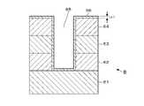
以下、成膜装置1によって行われる前処理及びSiN膜の成膜処理について、ウエハBの縦断側面図である図5~図9と、成膜装置1の動作のフローチャートである図10と、を参照しながら説明する。図5は、成膜装置1へ搬送されるウエハBの一例を示しており、当該ウエハBには、当該Si膜61、SiO2膜62、W膜63、SiO2膜64が、この順に上方へ向かって積層する積層体が形成されている。この積層体には凹部65が形成されており、凹部65の側面がSiO2膜62、W膜63、SiO2膜64により構成され、凹部65の底面がSi膜61により構成されている。従って、既述したようにウエハBの表面において、Si膜、SiO2膜、W膜が各々露出している。5 to 9, which are longitudinal side views of the wafer B, and FIG. 10, which is a flow chart of the operation of the
この図5に示すウエハBが6枚、回転テーブル12の凹部14に各々載置される。そして、真空容器11の搬送口16に設けられるゲートバルブを閉鎖して当該真空容器11内が気密にされ、ウエハBはヒーター15によって例えば200℃~600℃、より具体的には例えば550℃に加熱される。そして、排気口51からの排気によって、真空容器11内が例えば53.3Pa~666.5Paである真空雰囲気にされると共に、回転テーブル12が例えば3rpm~60rpmで回転して、各ウエハBが公転する。Six wafers B shown in FIG. Then, the gate valve provided at the
プラズマ形成ユニット3A~3Cによりプラズマ形成領域R1~R3においては、H2ガスの供給とマイクロ波の供給とが行われ、H2ガスのプラズマが各々形成される。その一方で、シャワーヘッド2においてはガス吐出口21からHCDガス、パージガス吐出口23からArガスが夫々吐出されると共に、排気口22から排気が行われる(図10中、ステップS1)。このようにシャワーヘッド2及びプラズマ形成ユニット3A~3Cが動作することで、公転する各ウエハBに、HCDガスの供給とプラズマ化したH2ガスの供給とが、交互に繰り返し行われる。In the plasma forming regions R1 to R3, the
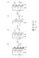
図11はこのように前処理が行われるときにSiO2膜64の表面で起きていると考えられる反応を模式的に示しており、図中の71はSi原子、72はO原子、73はHCD分子を夫々表している。ウエハBがプラズマ形成領域R1~R3に位置し、プラズマを構成するH2ガスの活性種(Hラジカルなど)がSiO2膜64の表面のO原子72と反応する。それにより、このO原子72はH2OとなってSiO2膜64から脱離し、SiO2膜64の表面は還元される(図11(a))。その結果として、当該SiO2膜64の表面は、Si原子71が比較的多い状態となる。FIG. 11 schematically shows reactions that are thought to occur on the surface of the SiO2 film 64 when such pretreatment is performed. Each represents an HCD molecule. Wafer B is positioned in plasma formation regions R1 to R3, and active species (H radicals, etc.) of H2 gas forming plasma react with
続いてウエハBが吸着領域R0に位置し、還元されたSiO2膜64の表面にHCD分子73が供給される(図11(b))。上記のようにHラジカルによって還元されることで、SiO2膜64の表面は活性化されて、供給されるHCD分子73が吸着されやすい状態になっていると考えられ、効率良く吸着が進む。このようにHCD分子73が吸着した状態で、ウエハBがプラズマ形成領域R1~R3に再度位置すると、H2ガスの活性種が吸着したHCD分子73に含まれるCl(塩素)原子と反応する。それにより、HCD分子73のCl原子はHCl(塩酸)となってSiO2膜64から脱離し、SiO2膜64の表面にはHCD分子73から生じたSi原子71が吸着した状態となる。Subsequently, the wafer B is positioned in the adsorption region R0, and
SiO2膜64の表面の変化について説明したが、SiO2膜62の表面についてもSiO2膜と同様に表面のO原子72が除去されて、Si原子71が吸着される。また、Si膜61については、表面がSi原子71により構成されるため、HCD分子73の吸着が起こりやすいので、SiO2膜62、64と同様にHCD分子73に含まれているSi原子71が吸着される。W膜63については、SiO2膜62、64と同様に、Hラジカルによる表面の還元、活性化により、HCD分子73が比較的多く吸着されると考えられる。即ち、Si膜61、SiO2膜62、64、W膜63の表面には、夫々効率良くSi原子71が吸着される。ウエハBの公転が続けられ、吸着領域R0とプラズマ形成領域R1~R3とをウエハBが繰り返し移動することで、このようなSi原子71の吸着が進行し、ウエハBの表面全体を被覆するようにSiの薄層66が形成される(図6、図11(c))。Although the change in the surface of the SiO2 film 64 has been described, the
シャワーヘッド2からのHCDガスの供給及びプラズマ形成ユニット3A~3CによるH2プラズマの形成が開始されてから回転テーブル12が予め設定された回数、例えば30回回転すると、シャワーヘッド2からのHCDガスの供給が停止する。このようにHCDガスの供給が停止する一方で、プラズマ形成領域R1~R3にはH2ガスとNH3ガスとが供給され、これらのガスのプラズマが形成される(ステップS2)。そしてウエハBの公転が続けられ、各ウエハBはプラズマ形成領域R1~R3を繰り返し通過する。それにより、プラズマを構成するNH3ガスの活性種(NH2ラジカル、NHラジカルなど)がSiの薄層66と反応し、当該薄層66は窒化されてSiNの薄層67となる(図7、図11(d))。なお、図11(d)における74は窒素原子を示している。When the rotary table 12 rotates a preset number of times, for example, 30 times after the supply of HCD gas from the
H2ガス及びNH3ガスのプラズマの形成開始から回転テーブル12が予め設定された回数を回転すると、シャワーヘッド2から吸着領域R0へのHCDガスの供給が再開される。また、プラズマ形成領域R1、R2においてはNH3ガスの供給が停止する一方、H2ガスは引き続き供給され、当該H2ガスのプラズマが形成される。プラズマ形成領域R3においては引き続きH2ガス及びNH3ガスが供給され、これらのガスのプラズマが形成される(ステップS3)。When the rotary table 12 rotates a preset number of times from the start of plasma formation of H2 gas and NH3 gas, the supply of HCD gas from the
そして、ウエハBは引き続き公転し、吸着領域R0におけるHCDガスの供給、プラズマ形成領域R1、R2におけるプラズマ化したH2ガスの供給、プラズマ形成領域R3におけるプラズマ化したH2ガス及びNH3ガスの供給が、順次繰り返し行われる。吸着領域R0でウエハBに吸着されたHCDガス中のSiがプラズマ形成領域R3で窒化され、SiNとなる。そしてプラズマ形成領域R1、R2では、H2ガスのプラズマにより、堆積したSiNの改質が行われる。具体的に、SiN中の未結合手に対するHの結合及び堆積したSiNからのClの除去が行われることで、緻密で不純物の含有量が少ないSiNとなる。Then, the wafer B continues to revolve, supplying HCD gas in the adsorption region R0, supplying plasma H2 gas in the plasma forming regions R1 and R2, and supplying plasma H2 gas and NH3 gas in the plasma forming region R3. The feeding is repeated sequentially. Si in the HCD gas adsorbed on the wafer B in the adsorption region R0 is nitrided in the plasma formation region R3 to become SiN. Then, in the plasma forming regions R1 andR2 , the deposited SiN is reformed by plasma of H2 gas. Specifically, bonding of H to dangling bonds in SiN and removal of Cl from the deposited SiN are performed, resulting in dense SiN with a low content of impurities.
既述したようにSiNの核の形成と成長とが起きるが、下地が当該核と同じSiNである薄層67であるため、この核の形成と成長とは比較的速やかに行われる。そして、Si膜61、SiO2膜62、64及びW膜63の各膜上に、そのような共通のSiNの薄層67が形成されており、これらの各膜の表面の状態が揃えられている。従って、これらの各膜上で核の形成と成長とが同様に起こり、SiNの薄層(SiN膜68)が成膜される。つまり、Si膜61、SiO2膜62、64及びW膜63の各膜上において、あたかもインキュベーションタイムが揃うようにSiN膜68の成膜が行われる(図8)。As described above, the formation and growth of SiN nuclei occur, but since the underlying layer is the
ウエハBの公転が続けられ、SiN膜68の膜厚が上昇すると共に当該SiN膜68の改質が進行する。上記のようにSi膜61、SiO2膜62、64、W膜63の各膜上にて同様のタイミングでSiN膜68の成膜が開始されるので、これらの各膜間で均一性高い膜厚で当該SiN膜68が成長する。ステップS3におけるHCDガスの供給及びプラズマ形成領域R1~R3における各ガスのプラズマ化が開始されてから予め設定された回数を回転テーブル12が回転し、所望の膜厚のSiN膜67が形成されると、SiN膜68の成膜処理が終了する(図9)。つまり、各ガスの供給、マイクロ波の供給、回転テーブル12の回転が各々停止して成膜処理が終了する。然る後、ウエハBは、基板搬送機構によって真空容器11から搬出される。The wafer B continues to revolve, the film thickness of the
このように成膜装置1を用いた処理によれば、Si膜61、SiO2膜62、64及びW膜63間でのSiN膜68のインキュベーションタイムの差の影響が抑制され、成膜が開始されるタイミングを揃えることができる。その結果として、各膜上にて均一性高い膜厚となるように当該SiN膜68を成膜することができる。Thus, according to the process using the
なお、Siの薄層66から生成するSiNの薄層67と、SiN膜68とは製造手法が異なるので膜質が異なるものとなる場合が有るので、Siの薄層66の厚さが大きくなりすぎると、ウエハBから製造される製品の特性に影響を与えるおそれが有る。そのため上記の処理において、HCDガスの供給停止時におけるSiの薄層66の厚さH1(図6参照)は小さくすることが好ましく、例えば1nm以下とすることが好ましい。Note that the SiN
ところで上記のステップS1で形成されたSiの薄層66の窒化を、N2ガスのプラズマにより行ってもよい。ただし、薄層66から生成するSiNの薄層67の膜質について、SiN膜68の膜質と同等の膜質とするために、上記のようにSiの薄層66の窒化は、NH3ガスのプラズマを用いて行うことが好ましい。なお、プラズマ化していないN2ガスやNH3ガスを供給することで、Siの薄層66の窒化を行うようにしてもよい。以上に述べたように、Siの薄層66の窒化については、NH3ガスのプラズマを用いることには限られない。By the way, the nitridation of the
また、SiNの薄層67形成後のSiN膜68の形成は、ALDで行うことに限られず、CVD(Chemical Vapor Deposition)で行ってもよい。このSiN膜68の形成においては、原料ガス中のシリコンを窒化できればよいので、プラズマ化したNH3ガスを用いることにも限られず、例えばプラズマ化してないNH3ガスを用いてもよい。Further, the formation of the
また、Siの薄層66を形成するにあたり、HCDガスを用いることには限られず、ジクロロシラン(DCS)ガスなどのシリコンの塩化物により構成されるガスを用いてもよい。また、シリコンと、例えばヨウ素などの塩素以外のハロゲンと、により構成されるハロゲン化シリコンガスを用いて、Siの薄層66を形成してもよい。ただし、既述したように1分子中にSiを多く含み、多くのSiを効率良くウエハBに吸着させることができるため、HCDガスを用いることが好ましい。また、上記の処理例ではSiの薄層66を形成するための処理ガス及びSiN膜68を成膜するために用いられるシリコンを含む原料ガスとして同じHCDガスを用いているが、処理ガスと原料ガスとが異なるガスであってもよい。例えば、処理ガスとしてはHCDガスを用い、原料ガスとしてはDCSガスを用いてもよい。Further, in forming the
上記の処理例では金属膜としてW膜63上にSiN膜を形成しているが、W膜63に限られず、例えばTi(チタン)やNi(ニッケル)などの金属膜上にSiN膜68を形成する場合にも本手法が有効である。つまり、SiN膜の下地となる金属膜としては、W膜に限られるものではない。なお、今回開示された実施形態は、全ての点で例示であって制限的なものではないと考えられるべきである。上記の実施形態は、添付の特許請求の範囲及びその趣旨を逸脱することなく、様々な形態で省略、置換、変更されてもよい。In the above processing example, the SiN film is formed on the
以下、本技術に関連して行われた評価試験について説明する。
(評価試験1)
評価試験1として、Siにより構成されると共に表面が剥き出しの状態のウエハ(ベアウエハ)と、Siにより構成されると共に表面にSiO2膜が形成されたウエハ(SiO2ウエハとする)と、を複数枚ずつ用意した。そして、上記の実施形態で説明したステップS1~S3からなる一連の処理(前処理及びSiN膜68の成膜処理)を、ベアウエハ、SiO2ウエハに夫々行った。この一連の処理におけるステップS3のSiN膜68の成膜処理の時間は、180秒または360秒に設定した。一連の処理の終了後は、形成されたSiN膜68の膜厚を測定した。Evaluation tests conducted in relation to the present technology will be described below.
(Evaluation test 1)
As
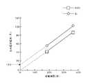
また比較試験1として、上記のステップS1の処理を行う代わりにプラズマ形成領域R1~R3にN2ガスを供給し、当該N2ガスをプラズマ化してベアウエハ、SiO2ウエハの表面を夫々窒化させる処理を行った。この窒化後は、各ウエハに既述のステップS2と、ステップS3とを行ったが、ステップS3の原料ガスとしてはHCDガスの代わりにDCSガスを用いた。このような差異点を除いて、比較試験1の処理は評価試験1の処理と同様である。In addition, as a
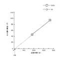
図12のグラフは評価試験1の結果を、図13のグラフは比較試験1の結果を夫々示している。各グラフについて横軸はステップS3のSiN膜68の成膜時間(単位:秒)であり、縦軸はSiN膜68の膜厚(Å)である。各グラフには、測定されたSiN膜68の膜厚をプロットして示すと共に、ベアウエハについてプロットされた各点を結ぶ実線の直線、SiO2ウエハについてプロットされた各点を結ぶ実線の直線を各々示している。さらにグラフには上記の各実線の直線を、横軸の成膜時間が0秒となる位置あるいは縦軸のSiN膜68の膜厚が0Åとなる位置まで伸ばした延長線について、点線で表示している。なお、膜についてのインキュベーションタイムを、その膜に直接接するようにSiN膜を成膜するときに成膜が開始するまでの時間として定義したが、その定義に関わらずこの評価試験では、上記の点線の延長線を見て膜厚が0Åであるときの成膜時間をインキュベーションタイムとする。The graph in FIG. 12 shows the results of the
評価試験1については、SiN膜68の成膜時間が180秒、360秒であるときのいずれにおいてもSiO2ウエハとベアウエハとの間で、SiN膜68の膜厚に差が殆ど見られなかった。そして、SiO2ウエハについてのインキュベーションタイムは9.8秒であり、ベアウエハについてのインキュベーションタイムも概ね9.8秒である。そして成膜時間が9.8秒であるときの膜厚差(ベアウエハのSiN膜68の膜厚-SiO2ウエハのSiN68の膜厚)は-0.6Å、即ち略0Åであった。つまり、SiO2ウエハ、ベアウエハのいずれにおいてもステップS3の開始後、概ね9.8秒経過すると、SiN膜68の成膜が開始されたことが確認された。Regarding the
一方、比較試験1については、SiN膜68の成膜時間が180秒、360秒であるときの夫々において、SiO2ウエハとベアウエハとの間でSiN膜68の膜厚に比較的大きな差が見られた。そして、SiO2ウエハについてのインキュベーションタイムは概ね0秒であるが、ベアウエハについては成膜時間が0秒であるときに、SiN膜68の膜厚が13.2Åである。このように成膜時間が0秒で既にSiN膜68が形成される結果となったのは、N2ガスのプラズマに曝されたことで、ベアウエハの表面が窒化されてSiNとなったことによると考えられる。このような評価試験1及び比較試験1の結果から、既述の実施形態で述べた手法によれば、Si膜とSiO2膜との間で膜厚を揃えることができることが確認された。On the other hand, in
(評価試験2)
評価試験2として、評価試験1と同様にベアウエハ、SiO2ウエハに各々上記のステップS1~S3からなる処理を行い、SiN膜68の膜厚を取得した。そして、図12で説明したようにSiN膜68の膜厚をグラフにプロットし、各プロットを結ぶ直線の延長線より、インキュベーションタイムを取得した。また、膜厚差(ベアウエハのSiN膜68の膜厚-SiO2ウエハのSiN膜68の膜厚)を算出した。(Evaluation test 2)
As
比較試験2-1として、前処理であるステップS1、S2を行わず、ステップS3のみを実施してベアウエハ、SiO2ウエハを各々処理した。比較試験2-2として、ステップS1、S2を行わず、公転するベアウエハ、SiO2ウエハに対してシャワーヘッド2よりHCDガスを供給した後に、ステップS3を行った。比較試験2-3として、ステップS1、S2を行わず、プラズマ形成領域R1~R3にH2ガスのプラズマを形成して、公転するベアウエハ、SiO2ウエハを各々当該H2プラズマに曝した後、ステップS3を行った。なお、このような差異点を除いて、比較試験2-1~2-3は、評価試験2と同様に処理を行った。比較試験2-1~2-3で処理された各ウエハについては、評価試験2と同様にインキュベーションタイムの取得と、上記の膜厚差の算出とを行った。As a comparative test 2-1, bare wafers and SiO2 wafers were processed by performing only step S3 without performing steps S1 and S2, which are pretreatments. As a comparative test 2-2, steps S1 and S2 were not performed, and step S3 was performed after HCD gas was supplied from the
図14のグラフは、評価試験2及び比較試験2-1~2-3の結果を示している。このグラフにおいては、取得されたインキュベーションタイム(単位:秒)についてプロットされ、ベアウエハについてプロットされた点同士が実線、SiO2ウエハについてプロットされた点同士が点線で夫々結ばれて示されている。また、棒グラフにより、上記の膜厚差(単位:Å)について示している。The graph in FIG. 14 shows the results of
グラフに示すように評価試験2に比べると評価試験2-1~2-3においては、SiウエハとSiO2ウエハとの間のインキュベーションタイムの差及び膜厚差が大きい。従って、上記の実施形態で説明した処理がこれらインキュベーションタイムの差及び膜厚差を低減させるために有効であることが示された。また、評価試験2、比較試験2-2、2-3の結果より、HCDの供給及びH2ガスのプラズマの供給のうち、いずれか一方のみを行った場合には十分な効果が得られず、十分な効果を得るためには、実施形態のステップS1のようにこれらの処理を両方行うことが必要であることが分かる。As shown in the graph, in evaluation tests 2-1 to 2-3, compared to
B ウエハ
1 成膜装置
10 制御部
12 回転テーブル
2 シャワーヘッド
3A~3C プラズマ形成ユニット
61 Si膜
62、64 SiO2膜、SiO2膜
63 W膜
66 Siの薄層
67 SiNの薄層
68 SiN膜
Claims (8)
Translated fromJapanese前記基板にプラズマ化した水素ガスを供給する工程と、
前記基板にハロゲン化シリコンにより構成される処理ガスを供給する工程と、
前記プラズマ化した水素ガスを供給する工程と前記処理ガスを供給する工程とを交互に繰り返し行い、前記第1の膜及び前記第2の膜を被覆するシリコンの薄層を形成する工程と、
前記シリコンの薄層を窒化する第2の窒化ガスを前記基板に供給して、窒化シリコンの薄層を形成する工程と、
前記原料ガスと、前記第1の窒化ガスとを前記基板に供給して、前記窒化シリコンの薄層上に前記窒化シリコン膜を成膜する工程と、
を備える成膜方法。A first film and a second film having different incubation times required to start growth of a silicon nitride film when a source gas containing silicon and a first nitriding gas for nitriding silicon are supplied. In the film formation method for forming the silicon nitride film on the substrate provided on the surface,
a step of supplying plasma hydrogen gas to the substrate;
supplying a process gas composed of a silicon halide to the substrate;
a step of alternately repeating the step of supplying the plasma hydrogen gas and the step of supplying the processing gas to form a thin silicon layer covering the first film and the second film;
supplying a second nitriding gas to the substrate to nitride the thin layer of silicon to form a thin layer of silicon nitride;
supplying the raw material gas and the first nitriding gas to the substrate to form the silicon nitride film on the silicon nitride thin layer;
A film forming method comprising:
前記基板を載置して公転させる回転テーブルと、
前記回転テーブル上にプラズマ化した水素ガスを供給する水素ガス供給部と、
前記回転テーブル上にハロゲン化シリコンにより構成される処理ガスを供給する処理ガス供給部と、
前記回転テーブル上に第1の窒化ガス、第2の窒化ガスを各々供給する窒化ガス供給部と、
前記回転テーブル上に前記原料ガスを供給する原料ガス供給部と、
前記第1の膜及び前記第2の膜を被覆するシリコンの薄層を形成するために、公転する前記基板に前記プラズマ化した水素ガスと前記処理ガスとを交互に繰り返し供給するステップと、前記シリコンの薄層を窒化して窒化シリコンの薄層を形成するために、公転する前記基板に前記第2の窒化ガスを供給するステップと、前記窒化シリコンの薄層上に前記窒化シリコン膜を成膜するために、公転する前記基板に前記原料ガスと前記第1の窒化ガスとを交互に繰り返し供給するステップと、を行うように構成された制御部と、
を備える成膜装置。A first film and a second film having different incubation times required to start growth of a silicon nitride film when a source gas containing silicon and a first nitriding gas for nitriding silicon are supplied. In a film forming apparatus for forming the silicon nitride film on a substrate provided on the surface,
a rotary table on which the substrate is placed and revolved;
a hydrogen gas supply unit that supplies plasma hydrogen gas onto the rotary table;
a processing gas supply unit that supplies a processing gas composed of silicon halide onto the rotary table;
a nitriding gas supply unit that supplies a first nitriding gas and a second nitriding gas onto the rotary table;
a raw material gas supply unit that supplies the raw material gas onto the rotary table;
alternately and repeatedly supplying the plasmatized hydrogen gas and the processing gas to the revolving substrate in order to form a thin silicon layer covering the first film and the second film; supplying the second nitriding gas to the revolving substrate to nitridize the thin layer of silicon to form a thin layer of silicon nitride; and forming the silicon nitride film on the thin layer of silicon nitride. a controller configured to alternately and repeatedly supply the source gas and the first nitriding gas to the revolving substrate in order to form a film;
A film forming apparatus.
前記回転テーブル上の前記第1の領域に対して当該回転テーブルの回転方向に離れ、且つ雰囲気が分離された第2の領域にガスを供給すると共に当該ガスをプラズマ化する第2のガス供給部と、
が設けられ、
前記原料ガス供給部及び前記処理ガス供給部は前記第1のガス供給部であり、
前記第1の窒化ガス及び前記第2の窒化ガスはプラズマ化された窒化ガスであり、前記窒化ガス供給部及び前記水素ガス供給部は前記第2のガス供給部である請求項7記載の成膜装置。a first gas supply unit that supplies gas to a first region on the rotary table;
A second gas supply unit for supplying a gas to a second region separated from the first region on the turntable in the rotation direction of the turntable and separated from the atmosphere and turning the gas into plasma. When,
is provided,
The raw material gas supply unit and the processing gas supply unit are the first gas supply unit,
8. The process according to claim 7, wherein said first nitriding gas and said second nitriding gas are plasma nitriding gases, and said nitriding gas supply section and said hydrogen gas supply section are said second gas supply section. membrane device.
Priority Applications (5)
| Application Number | Priority Date | Filing Date | Title |
|---|---|---|---|
| JP2019149953AJP7200880B2 (en) | 2019-08-19 | 2019-08-19 | Film forming method and film forming apparatus |
| CN202010788135.4ACN112391612B (en) | 2019-08-19 | 2020-08-07 | Film forming method and film forming apparatus |
| KR1020200098934AKR102772649B1 (en) | 2019-08-19 | 2020-08-07 | Film forming method and film forming apparatus |
| US16/989,103US20210054501A1 (en) | 2019-08-19 | 2020-08-10 | Film forming method and film forming apparatus |
| TW109127038ATWI851785B (en) | 2019-08-19 | 2020-08-10 | Film forming method and film forming device |
Applications Claiming Priority (1)
| Application Number | Priority Date | Filing Date | Title |
|---|---|---|---|
| JP2019149953AJP7200880B2 (en) | 2019-08-19 | 2019-08-19 | Film forming method and film forming apparatus |
Publications (2)
| Publication Number | Publication Date |
|---|---|
| JP2021034428A JP2021034428A (en) | 2021-03-01 |
| JP7200880B2true JP7200880B2 (en) | 2023-01-10 |
Family
ID=74603033
Family Applications (1)
| Application Number | Title | Priority Date | Filing Date |
|---|---|---|---|
| JP2019149953AActiveJP7200880B2 (en) | 2019-08-19 | 2019-08-19 | Film forming method and film forming apparatus |
Country Status (5)
| Country | Link |
|---|---|
| US (1) | US20210054501A1 (en) |
| JP (1) | JP7200880B2 (en) |
| KR (1) | KR102772649B1 (en) |
| CN (1) | CN112391612B (en) |
| TW (1) | TWI851785B (en) |
Families Citing this family (1)
| Publication number | Priority date | Publication date | Assignee | Title |
|---|---|---|---|---|
| JP2023118554A (en)* | 2022-02-15 | 2023-08-25 | 東京エレクトロン株式会社 | Method for forming silicon nitride film and film forming apparatus |
Citations (4)
| Publication number | Priority date | Publication date | Assignee | Title |
|---|---|---|---|---|
| US5939333A (en) | 1996-05-30 | 1999-08-17 | Micron Technology, Inc. | Silicon nitride deposition method |
| WO2013161768A1 (en) | 2012-04-23 | 2013-10-31 | 東京エレクトロン株式会社 | Film forming method, film forming device, and film forming system |
| JP2015097255A (en) | 2013-10-07 | 2015-05-21 | 東京エレクトロン株式会社 | Method and apparatus for forming silicon nitride film |
| JP2017175106A (en) | 2016-03-17 | 2017-09-28 | 東京エレクトロン株式会社 | Film forming method and film forming apparatus |
Family Cites Families (19)
| Publication number | Priority date | Publication date | Assignee | Title |
|---|---|---|---|---|
| US6881636B2 (en)* | 2003-07-03 | 2005-04-19 | Micron Technology, Inc. | Methods of forming deuterated silicon nitride-containing materials |
| KR100734393B1 (en)* | 2005-11-28 | 2007-07-02 | 주식회사 에이이티 | Atomic Layer Deposition of Silicon Thin Films |
| JP4983159B2 (en)* | 2006-09-01 | 2012-07-25 | 東京エレクトロン株式会社 | Process for oxidizing object, oxidation apparatus and storage medium |
| CN100554140C (en)* | 2006-11-23 | 2009-10-28 | 南京大学 | The preparation method of gas phase self-assembled growth silicon quantum torus nano structure |
| JP2008177419A (en)* | 2007-01-19 | 2008-07-31 | Nissin Electric Co Ltd | Silicon thin film formation method |
| KR101436564B1 (en)* | 2008-05-07 | 2014-09-02 | 한국에이에스엠지니텍 주식회사 | Forming method of amorphous silicone thin film |
| US8563095B2 (en)* | 2010-03-15 | 2013-10-22 | Applied Materials, Inc. | Silicon nitride passivation layer for covering high aspect ratio features |
| JP2013051370A (en)* | 2011-08-31 | 2013-03-14 | Tokyo Electron Ltd | Film forming method and storage medium |
| JP5925476B2 (en)* | 2011-12-09 | 2016-05-25 | 株式会社アルバック | Method for forming tungsten compound film |
| JP6011417B2 (en)* | 2012-06-15 | 2016-10-19 | 東京エレクトロン株式会社 | Film forming apparatus, substrate processing apparatus, and film forming method |
| JP6262115B2 (en)* | 2014-02-10 | 2018-01-17 | 東京エレクトロン株式会社 | Substrate processing method and substrate processing apparatus |
| US9576792B2 (en)* | 2014-09-17 | 2017-02-21 | Asm Ip Holding B.V. | Deposition of SiN |
| JP6800004B2 (en)* | 2016-02-01 | 2020-12-16 | 東京エレクトロン株式会社 | Method of forming a silicon nitride film |
| JP6656103B2 (en)* | 2016-07-15 | 2020-03-04 | 東京エレクトロン株式会社 | Method and apparatus for forming nitride film |
| JP6733516B2 (en)* | 2016-11-21 | 2020-08-05 | 東京エレクトロン株式会社 | Method of manufacturing semiconductor device |
| US20180245216A1 (en)* | 2017-02-28 | 2018-08-30 | Tokyo Electron Limited | Film forming apparatus |
| KR101967529B1 (en)* | 2017-06-12 | 2019-04-09 | 에스케이머티리얼즈 주식회사 | Forming method of silicon nitride film |
| JP6863107B2 (en)* | 2017-06-13 | 2021-04-21 | 東京エレクトロン株式会社 | Film forming equipment, cleaning method of film forming equipment and storage medium |
| JP6946769B2 (en)* | 2017-06-15 | 2021-10-06 | 東京エレクトロン株式会社 | Film formation method, film deposition equipment, and storage medium |
- 2019
- 2019-08-19JPJP2019149953Apatent/JP7200880B2/enactiveActive
- 2020
- 2020-08-07KRKR1020200098934Apatent/KR102772649B1/enactiveActive
- 2020-08-07CNCN202010788135.4Apatent/CN112391612B/enactiveActive
- 2020-08-10USUS16/989,103patent/US20210054501A1/ennot_activeAbandoned
- 2020-08-10TWTW109127038Apatent/TWI851785B/enactive
Patent Citations (4)
| Publication number | Priority date | Publication date | Assignee | Title |
|---|---|---|---|---|
| US5939333A (en) | 1996-05-30 | 1999-08-17 | Micron Technology, Inc. | Silicon nitride deposition method |
| WO2013161768A1 (en) | 2012-04-23 | 2013-10-31 | 東京エレクトロン株式会社 | Film forming method, film forming device, and film forming system |
| JP2015097255A (en) | 2013-10-07 | 2015-05-21 | 東京エレクトロン株式会社 | Method and apparatus for forming silicon nitride film |
| JP2017175106A (en) | 2016-03-17 | 2017-09-28 | 東京エレクトロン株式会社 | Film forming method and film forming apparatus |
Also Published As
| Publication number | Publication date |
|---|---|
| CN112391612B (en) | 2024-07-09 |
| TWI851785B (en) | 2024-08-11 |
| JP2021034428A (en) | 2021-03-01 |
| TW202117850A (en) | 2021-05-01 |
| CN112391612A (en) | 2021-02-23 |
| US20210054501A1 (en) | 2021-02-25 |
| KR102772649B1 (en) | 2025-02-25 |
| KR20210021918A (en) | 2021-03-02 |
Similar Documents
| Publication | Publication Date | Title |
|---|---|---|
| JP6690496B2 (en) | Film forming method and film forming apparatus | |
| TWI616926B (en) | Manufacturing method of semiconductor device, substrate processing device and recording medium | |
| JP6863107B2 (en) | Film forming equipment, cleaning method of film forming equipment and storage medium | |
| US10438791B2 (en) | Film forming method, film forming apparatus, and storage medium | |
| JP2020161722A (en) | Substrate processing method and substrate processing device | |
| JP2015010271A (en) | Deposition method | |
| JP2012059997A (en) | Semiconductor device manufacturing method and substrate processing apparatus | |
| US9922820B2 (en) | Film forming method and film forming apparatus | |
| JP7200880B2 (en) | Film forming method and film forming apparatus | |
| JP7243521B2 (en) | Film forming method and film forming apparatus | |
| JP7040257B2 (en) | Film forming equipment and film forming method | |
| JP6988629B2 (en) | Film formation method and film formation equipment | |
| JP6544232B2 (en) | Film forming method and film forming apparatus | |
| WO2018163399A1 (en) | Substrate treatment device, method for manufacturing semiconductor device, and program | |
| JP2018137293A (en) | Film deposition device | |
| JP2018081964A (en) | Deposition equipment | |
| JP2021039975A (en) | Film deposition apparatus and film deposition method | |
| JP7247813B2 (en) | Film forming method and film forming apparatus | |
| US12424463B2 (en) | Method of processing substrate, method of manufacturing semiconductor device, substrate processing system, and recording medium | |
| JP7330091B2 (en) | Deposition method | |
| JP2022120422A (en) | Deposition method | |
| JP2025077182A (en) | Film forming method and film forming apparatus | |
| JP2022049442A (en) | Deposition method |
Legal Events
| Date | Code | Title | Description |
|---|---|---|---|
| A621 | Written request for application examination | Free format text:JAPANESE INTERMEDIATE CODE: A621 Effective date:20220221 | |
| TRDD | Decision of grant or rejection written | ||
| A977 | Report on retrieval | Free format text:JAPANESE INTERMEDIATE CODE: A971007 Effective date:20221116 | |
| A01 | Written decision to grant a patent or to grant a registration (utility model) | Free format text:JAPANESE INTERMEDIATE CODE: A01 Effective date:20221122 | |
| A61 | First payment of annual fees (during grant procedure) | Free format text:JAPANESE INTERMEDIATE CODE: A61 Effective date:20221205 | |
| R150 | Certificate of patent or registration of utility model | Ref document number:7200880 Country of ref document:JP Free format text:JAPANESE INTERMEDIATE CODE: R150 |