JP7192121B2 - Formation of staircase structures in three-dimensional memory devices - Google Patents
Formation of staircase structures in three-dimensional memory devicesDownload PDFInfo
- Publication number
- JP7192121B2 JP7192121B2JP2021530980AJP2021530980AJP7192121B2JP 7192121 B2JP7192121 B2JP 7192121B2JP 2021530980 AJP2021530980 AJP 2021530980AJP 2021530980 AJP2021530980 AJP 2021530980AJP 7192121 B2JP7192121 B2JP 7192121B2
- Authority
- JP
- Japan
- Prior art keywords
- layer
- staircase structure
- stack
- staircase
- regions
- Prior art date
- Legal status (The legal status is an assumption and is not a legal conclusion. Google has not performed a legal analysis and makes no representation as to the accuracy of the status listed.)
- Active
Links
Images


Classifications
- H—ELECTRICITY
- H01—ELECTRIC ELEMENTS
- H01L—SEMICONDUCTOR DEVICES NOT COVERED BY CLASS H10
- H01L21/00—Processes or apparatus adapted for the manufacture or treatment of semiconductor or solid state devices or of parts thereof
- H01L21/70—Manufacture or treatment of devices consisting of a plurality of solid state components formed in or on a common substrate or of parts thereof; Manufacture of integrated circuit devices or of parts thereof
- H01L21/71—Manufacture of specific parts of devices defined in group H01L21/70
- H01L21/768—Applying interconnections to be used for carrying current between separate components within a device comprising conductors and dielectrics
- H01L21/76801—Applying interconnections to be used for carrying current between separate components within a device comprising conductors and dielectrics characterised by the formation and the after-treatment of the dielectrics, e.g. smoothing
- H01L21/76802—Applying interconnections to be used for carrying current between separate components within a device comprising conductors and dielectrics characterised by the formation and the after-treatment of the dielectrics, e.g. smoothing by forming openings in dielectrics
- H01L21/76816—Aspects relating to the layout of the pattern or to the size of vias or trenches
- H—ELECTRICITY
- H01—ELECTRIC ELEMENTS
- H01L—SEMICONDUCTOR DEVICES NOT COVERED BY CLASS H10
- H01L21/00—Processes or apparatus adapted for the manufacture or treatment of semiconductor or solid state devices or of parts thereof
- H01L21/02—Manufacture or treatment of semiconductor devices or of parts thereof
- H01L21/04—Manufacture or treatment of semiconductor devices or of parts thereof the devices having potential barriers, e.g. a PN junction, depletion layer or carrier concentration layer
- H01L21/18—Manufacture or treatment of semiconductor devices or of parts thereof the devices having potential barriers, e.g. a PN junction, depletion layer or carrier concentration layer the devices having semiconductor bodies comprising elements of Group IV of the Periodic Table or AIIIBV compounds with or without impurities, e.g. doping materials
- H01L21/30—Treatment of semiconductor bodies using processes or apparatus not provided for in groups H01L21/20 - H01L21/26
- H01L21/31—Treatment of semiconductor bodies using processes or apparatus not provided for in groups H01L21/20 - H01L21/26 to form insulating layers thereon, e.g. for masking or by using photolithographic techniques; After treatment of these layers; Selection of materials for these layers
- H01L21/3105—After-treatment
- H01L21/311—Etching the insulating layers by chemical or physical means
- H01L21/31105—Etching inorganic layers
- H01L21/31111—Etching inorganic layers by chemical means
- H—ELECTRICITY
- H01—ELECTRIC ELEMENTS
- H01L—SEMICONDUCTOR DEVICES NOT COVERED BY CLASS H10
- H01L21/00—Processes or apparatus adapted for the manufacture or treatment of semiconductor or solid state devices or of parts thereof
- H01L21/02—Manufacture or treatment of semiconductor devices or of parts thereof
- H01L21/04—Manufacture or treatment of semiconductor devices or of parts thereof the devices having potential barriers, e.g. a PN junction, depletion layer or carrier concentration layer
- H01L21/18—Manufacture or treatment of semiconductor devices or of parts thereof the devices having potential barriers, e.g. a PN junction, depletion layer or carrier concentration layer the devices having semiconductor bodies comprising elements of Group IV of the Periodic Table or AIIIBV compounds with or without impurities, e.g. doping materials
- H01L21/30—Treatment of semiconductor bodies using processes or apparatus not provided for in groups H01L21/20 - H01L21/26
- H01L21/31—Treatment of semiconductor bodies using processes or apparatus not provided for in groups H01L21/20 - H01L21/26 to form insulating layers thereon, e.g. for masking or by using photolithographic techniques; After treatment of these layers; Selection of materials for these layers
- H01L21/3105—After-treatment
- H01L21/311—Etching the insulating layers by chemical or physical means
- H01L21/31144—Etching the insulating layers by chemical or physical means using masks
- H—ELECTRICITY
- H01—ELECTRIC ELEMENTS
- H01L—SEMICONDUCTOR DEVICES NOT COVERED BY CLASS H10
- H01L21/00—Processes or apparatus adapted for the manufacture or treatment of semiconductor or solid state devices or of parts thereof
- H01L21/70—Manufacture or treatment of devices consisting of a plurality of solid state components formed in or on a common substrate or of parts thereof; Manufacture of integrated circuit devices or of parts thereof
- H01L21/71—Manufacture of specific parts of devices defined in group H01L21/70
- H01L21/768—Applying interconnections to be used for carrying current between separate components within a device comprising conductors and dielectrics
- H01L21/76838—Applying interconnections to be used for carrying current between separate components within a device comprising conductors and dielectrics characterised by the formation and the after-treatment of the conductors
- H01L21/76877—Filling of holes, grooves or trenches, e.g. vias, with conductive material
- H—ELECTRICITY
- H01—ELECTRIC ELEMENTS
- H01L—SEMICONDUCTOR DEVICES NOT COVERED BY CLASS H10
- H01L23/00—Details of semiconductor or other solid state devices
- H01L23/52—Arrangements for conducting electric current within the device in operation from one component to another, i.e. interconnections, e.g. wires, lead frames
- H01L23/522—Arrangements for conducting electric current within the device in operation from one component to another, i.e. interconnections, e.g. wires, lead frames including external interconnections consisting of a multilayer structure of conductive and insulating layers inseparably formed on the semiconductor body
- H01L23/5226—Via connections in a multilevel interconnection structure
- H—ELECTRICITY
- H01—ELECTRIC ELEMENTS
- H01L—SEMICONDUCTOR DEVICES NOT COVERED BY CLASS H10
- H01L23/00—Details of semiconductor or other solid state devices
- H01L23/52—Arrangements for conducting electric current within the device in operation from one component to another, i.e. interconnections, e.g. wires, lead frames
- H01L23/522—Arrangements for conducting electric current within the device in operation from one component to another, i.e. interconnections, e.g. wires, lead frames including external interconnections consisting of a multilayer structure of conductive and insulating layers inseparably formed on the semiconductor body
- H01L23/528—Layout of the interconnection structure
- H01L23/5283—Cross-sectional geometry
- H—ELECTRICITY
- H10—SEMICONDUCTOR DEVICES; ELECTRIC SOLID-STATE DEVICES NOT OTHERWISE PROVIDED FOR
- H10B—ELECTRONIC MEMORY DEVICES
- H10B41/00—Electrically erasable-and-programmable ROM [EEPROM] devices comprising floating gates
- H10B41/20—Electrically erasable-and-programmable ROM [EEPROM] devices comprising floating gates characterised by three-dimensional arrangements, e.g. with cells on different height levels
- H10B41/23—Electrically erasable-and-programmable ROM [EEPROM] devices comprising floating gates characterised by three-dimensional arrangements, e.g. with cells on different height levels with source and drain on different levels, e.g. with sloping channels
- H10B41/27—Electrically erasable-and-programmable ROM [EEPROM] devices comprising floating gates characterised by three-dimensional arrangements, e.g. with cells on different height levels with source and drain on different levels, e.g. with sloping channels the channels comprising vertical portions, e.g. U-shaped channels
- H—ELECTRICITY
- H10—SEMICONDUCTOR DEVICES; ELECTRIC SOLID-STATE DEVICES NOT OTHERWISE PROVIDED FOR
- H10B—ELECTRONIC MEMORY DEVICES
- H10B41/00—Electrically erasable-and-programmable ROM [EEPROM] devices comprising floating gates
- H10B41/50—Electrically erasable-and-programmable ROM [EEPROM] devices comprising floating gates characterised by the boundary region between the core region and the peripheral circuit region
- H—ELECTRICITY
- H10—SEMICONDUCTOR DEVICES; ELECTRIC SOLID-STATE DEVICES NOT OTHERWISE PROVIDED FOR
- H10B—ELECTRONIC MEMORY DEVICES
- H10B43/00—EEPROM devices comprising charge-trapping gate insulators
- H10B43/20—EEPROM devices comprising charge-trapping gate insulators characterised by three-dimensional arrangements, e.g. with cells on different height levels
- H10B43/23—EEPROM devices comprising charge-trapping gate insulators characterised by three-dimensional arrangements, e.g. with cells on different height levels with source and drain on different levels, e.g. with sloping channels
- H10B43/27—EEPROM devices comprising charge-trapping gate insulators characterised by three-dimensional arrangements, e.g. with cells on different height levels with source and drain on different levels, e.g. with sloping channels the channels comprising vertical portions, e.g. U-shaped channels
- H—ELECTRICITY
- H10—SEMICONDUCTOR DEVICES; ELECTRIC SOLID-STATE DEVICES NOT OTHERWISE PROVIDED FOR
- H10B—ELECTRONIC MEMORY DEVICES
- H10B43/00—EEPROM devices comprising charge-trapping gate insulators
- H10B43/50—EEPROM devices comprising charge-trapping gate insulators characterised by the boundary region between the core and peripheral circuit regions
Landscapes
- Engineering & Computer Science (AREA)
- Physics & Mathematics (AREA)
- Condensed Matter Physics & Semiconductors (AREA)
- General Physics & Mathematics (AREA)
- Computer Hardware Design (AREA)
- Microelectronics & Electronic Packaging (AREA)
- Power Engineering (AREA)
- Manufacturing & Machinery (AREA)
- Chemical & Material Sciences (AREA)
- Chemical Kinetics & Catalysis (AREA)
- General Chemical & Material Sciences (AREA)
- Inorganic Chemistry (AREA)
- Geometry (AREA)
- Semiconductor Memories (AREA)
- Non-Volatile Memory (AREA)
- Thin Film Transistor (AREA)
- Drying Of Semiconductors (AREA)
- Weting (AREA)
Description
Translated fromJapanese本開示の実施形態は、3次元(3D)メモリデバイス及びその製造方法に関する。 Embodiments of the present disclosure relate to three-dimensional (3D) memory devices and methods of manufacturing the same.
プレーナメモリセルは、プロセス技術、回路設計、プログラミングアルゴリズムおよび製造プロセスを改善することによってより小さく縮小される。しかし、メモリセルの特徴体の大きさが下限に近付くにつれて、プレーナプロセス及び製造技術は困難になり、高コストになる。結果として、プレーナメモリセルのメモリ密度は上限に近づいている。 Planar memory cells are shrunk smaller by improving process technology, circuit design, programming algorithms and manufacturing processes. However, as memory cell feature sizes approach the lower bounds, planar processes and manufacturing techniques become difficult and costly. As a result, the memory density of planar memory cells is approaching its upper limit.
3Dメモリアーキテクチャは、プレーナメモリセルの密度限界に対処しうる。3Dメモリアーキテクチャは、メモリアレイ及び、メモリアレイへ、及びメモリアレイからの信号を制御するための周辺デバイスを含む。典型的な3Dメモリアーキテクチャは、基板上に配置されたゲート電極と、基板内へのワード線を通り、交差する複数の半導体チャネルとの積層体を含む。ワード線と半導体チャネルとの交点が、メモリセルを形成する。 A 3D memory architecture can address the density limitations of planar memory cells. A 3D memory architecture includes a memory array and peripheral devices for controlling signals to and from the memory array. A typical 3D memory architecture includes a stack of gate electrodes disposed over a substrate and multiple intersecting semiconductor channels passing through word lines into the substrate. The intersections of word lines and semiconductor channels form memory cells.
3Dメモリアーキテクチャは、個別のメモリセルそれぞれの制御を可能にする電気接点スキームを必要とする。1つの電気接点スキームは、個別のメモリセルそれぞれのワード線へ接続するための階段構造を形成することである。階段構造は、典型的な3Dメモリデバイスにおいて半導体チャネルに沿って32本を超えるワード線を接続するのに使用されてきた。 A 3D memory architecture requires an electrical contact scheme that allows control of each individual memory cell. One electrical contact scheme is to form a staircase structure for connection to the word lines of each individual memory cell. A staircase structure has been used to connect more than 32 word lines along a semiconductor channel in a typical 3D memory device.
半導体技術が進歩するにつれて、3D NANDメモリデバイスなどの3Dメモリデバイスは、酸化物/窒化物(ON)層が増加し続けている。結果として、そのような階段構造を形成するために使用される既存の複数サイクルトリム及びエッチングプロセスは、スループットが低く、高額である。 As semiconductor technology advances, 3D memory devices, such as 3D NAND memory devices, continue to have an increasing oxide/nitride (ON) layer. As a result, existing multi-cycle trim and etch processes used to form such stepped structures have low throughput and are expensive.
3Dメモリデバイスの階段構造を形成するための方法の実施形態が、本明細書において開示される。開示される構造及び方法は、3Dメモリデバイスの製造の複雑さ及び製造コストの低減を含むがこれに限定しない多数の利益を提供する。 Embodiments of methods for forming a staircase structure of a 3D memory device are disclosed herein. The disclosed structures and methods provide a number of benefits including, but not limited to, reduced manufacturing complexity and cost of manufacturing 3D memory devices.
いくつかの実施形態において、3Dメモリデバイスを形成するための方法は、基板の上に配置された複数の誘電体層の対を含む交互層積層体を形成する段階と、交互層積層体の上に第1のマスク積層体を形成する段階と、交互層積層体の上にN個のサブ階段構造領域を含む階段構造領域を画定するために、第1のマスク積層体をパターニングする段階であって、Nが1より大きい、第1のマスク積層体をパターニングする段階と、階段構造領域の上に第1の階段構造を形成する段階であって、第1の階段構造が階段構造領域のそれぞれにおいてM個のステップを有し、Mが1より大きい、第1の階段構造を形成する段階と、第1の階段構造の上に第2の階段構造を形成する段階と、を含み、第2の階段構造が、階段構造領域において2*N*M個のステップを有する。いくつかの実施形態において、本方法は、基板上の積層記憶領域の複数の垂直半導体チャネルを形成する段階をさらに含む。いくつかの実施形態において、階段構造領域のそれぞれが、積層記憶領域に隣接する。 In some embodiments, a method for forming a 3D memory device includes forming an alternating layer stack including a plurality of pairs of dielectric layers disposed over a substrate; and patterning the first mask stack to define a stepped region including N sub-stepped regions on the alternating layer stack. patterning a first mask stack, wherein N is greater than 1; and forming a first staircase structure over the staircase structure region, the first staircase structure overlying each of the staircase structure regions. forming a first staircase structure having M steps in, where M is greater than 1; forming a second staircase structure over the first staircase structure; has 2*N*M steps in the stair structure area. In some embodiments, the method further includes forming a plurality of vertical semiconductor channels of stacked storage regions on the substrate. In some embodiments, each of the staircase regions adjoins a stacked storage region.
いくつかの実施形態において、3Dメモリデバイスは、基板上に配置された交互層積層体と、複数の垂直半導体チャネルを含む記憶構造と、記憶構造に隣接する複数の階段構造領域と、交互層積層体の複数の層積層体の一部を露出するために階段構造領域のそれぞれに配置された階段構造と、を含む。いくつかの実施形態において、階段構造がN個のサブ階段構造領域を含み、Nが1より大きい。いくつかの実施形態において、N個のサブ階段構造領域のそれぞれが2*M個のステップを含み、Mが1より大きい。 In some embodiments, a 3D memory device includes an alternating layer stack disposed on a substrate, a storage structure including a plurality of vertical semiconductor channels, a plurality of stepped regions adjacent to the storage structure, and an alternating layer stack. a stepped structure positioned in each of the stepped structure regions to expose a portion of the plurality of layer stacks of the body. In some embodiments, the step structure includes N sub-step structure regions, where N is greater than one. In some embodiments, each of the N sub-step structure regions includes 2*M steps, where M is greater than one.
本開示のその他の態様は、本開示の説明、特許請求の範囲及び図面に照らせば当業者は理解できるであろう。 Other aspects of the disclosure will be apparent to those of ordinary skill in the art in light of the description, claims and drawings of the disclosure.
本明細書に組み込まれ、明細書の一部をなす添付した図面は、本開示の実施形態を例示し、説明とともに、本開示の原理を説明する役割をさらに果たし、当業者は本開示の実施及び使用が可能になる。 The accompanying drawings, which are incorporated in and constitute a part of the specification, illustrate embodiments of the disclosure and, together with the description, serve to further explain the principles of the disclosure and enable those skilled in the art to practice the disclosure. and can be used.
特定の構成および配置が議論されるが、これは例示の目的のためにのみなされることは理解されるべきである。当業者であれば、他の構成および配置が、本開示の思想及び範囲を逸脱することなく使用されうることを認識するであろう。本開示はまた、様々な他の用途において採用されうることは当業者には明らかであろう。 Although specific configurations and arrangements are discussed, it should be understood that this is done for illustrative purposes only. A person skilled in the relevant art will recognize that other configurations and arrangements can be used without departing from the spirit and scope of this disclosure. It will be apparent to those skilled in the art that the present disclosure can also be employed in a variety of other applications.
明細書における「1つの実施形態」、「ある実施形態」、「ある例示的な実施形態」、「いくつかの実施形態」などの言及は、説明される実施形態が特定の特徴物、構造または特性を含みうるが、全ての実施形態が、必ずしも特定の特徴体、構造または特性を含むことができるわけではないことを示すことに注意すべきである。さらに、そのような語句は、必ずしも同じ実施形態を指しているわけではない。さらに、特定の特徴体、構造または特性がある実施形態に関して説明される場合、他の実施形態に関してそのような特徴体、構造または特性に影響を与えることは、明示されているか否かによらず、当業者の知識の範囲内である。 References in the specification to "one embodiment," "an embodiment," "an exemplary embodiment," "some embodiments," and the like may mean that the described embodiments may have particular features, structures or It should be noted that although properties may be included, not all embodiments may necessarily include a particular feature, structure or property. Moreover, such phrases are not necessarily referring to the same embodiment. Further, if a particular feature, structure or characteristic is described with respect to one embodiment, it is not expressly stated that it will affect such feature, structure or characteristic with respect to other embodiments. , is within the knowledge of a person skilled in the art.
一般に、用語は文脈の中での使用から少なくとも部分的に理解可能である。例えば、本明細書で使用されるように「1つまたは複数の」との用語は、少なくとも部分的に文脈に応じて、単数形で任意の特徴体、構造または特性を説明するために使用され、または複数形で特徴体、構造または特性の組み合わせを説明するために使用されうる。同様に、「1つの」、「ある」または「その」との用語も、少なくとも部分的に文脈に応じて、単数での使用を表し、または複数での使用を表すと理解可能である。さらに、「基づいて」との用語は、必ずしも因子の排他的なセットを伝えることを意図していないと理解可能であり、その代わりに、やはり少なくとも部分的に文脈に応じて、追加的な因子の存在が必ずしも明示されていない場合を許容しうる。 Generally, terms are at least partially intelligible from their use in context. For example, as used herein, the term "one or more" is used to describe any feature, structure or property in the singular, at least in part depending on the context. , or plural may be used to describe a combination of features, structures, or properties. Similarly, the terms "a", "a" or "the" can also be understood to refer to use in the singular or to refer to use in the plural, depending at least in part on the context. Moreover, it is to be understood that the term "based on" is not necessarily intended to convey an exclusive set of factors; instead, it is also at least partially context dependent that additional factors It is permissible that the existence of is not necessarily specified.
本開示において、「上」、「上に」及び「上方」の意味は、「上」が何かの「上に直接」を意味するだけではなく、その間に、介在する特徴体または層を有して何かの「上に」あるという意味を含むように、最も広く解釈されるべきであることは容易に理解されるべきである。さらに、「上に」または「上方に」は、何かの「上に」または「上方に」あることを意味するだけでなく、その間に、介在する特徴体または層がなく何かの「上に」または「上方に」(すなわち、何かの上に直接)あるという意味も含みうる。 In this disclosure, the meanings of "above," "above," and "above" do not only mean "directly on" what "above" is, but also have intervening features or layers therebetween. It should be readily understood that should be interpreted most broadly to include the meaning of being "on" something. Further, "on" or "above" means not only "on" or "above" something, but also something "above" without intervening features or layers therebetween. It can also include the meaning of being "on" or "above" (ie, directly on something).
さらに、「下」、「下に」、「より下方に」、「上方に」、「より上に」などの空間的に相対的な用語は、本明細書では1つの要素または特徴体の、他の要素または特徴体に対する関係を、図面に示されるように説明するための説明を容易にするために使用されうる。空間的に相対的な用語は、図面内に示された配向に加えて、使用時または動作時のデバイスの異なる配向も包含することを意図される。装置は、他の向き(90°回転させたり、他の向きにしたり)にすることもでき、本明細書で使用される空間的に相対的な記載も、それに応じて同様に解釈可能である。 Furthermore, spatially relative terms such as "below," "below," "below," "above," and "above" are used herein to refer to the It may be used to facilitate description to describe the relationship to other elements or features as shown in the drawings. Spatially relative terms are intended to encompass different orientations of the device in use or operation in addition to the orientation shown in the drawings. The device can be oriented in other ways (rotated 90° or otherwise oriented), and the spatially relative statements used herein can be similarly interpreted accordingly. .
本明細書で使用されるように、「基板」との用語は、後続の材料層が上に追加される材料を指す。基板は、上面及び底面を含む。基板の上面は、半導体デバイスが形成される場所であり、そのため半導体デバイスは基板の上面に形成される。底面は上面の反対側であり、そのため基板の底面側は基板の上面側の反対側である。基板それ自体はパターニングされうる。基板の上面に追加される材料は、パターニングされ、またはパターニングされないままにされうる。さらに、基板は、シリコン、ゲルマニウム、ガリウムヒ素、インジウムリンなどの幅広い範囲の半導体材料を含みうる。代替的に、基板は、ガラス、プラスチックまたはサファイアウェハーなどの非導電性材料で形成することも可能である。 As used herein, the term "substrate" refers to the material upon which subsequent layers of material are added. The substrate includes a top surface and a bottom surface. The top surface of the substrate is where the semiconductor devices are formed, so the semiconductor devices are formed on the top surface of the substrate. The bottom surface is opposite the top surface, so the bottom side of the substrate is opposite the top side of the substrate. The substrate itself can be patterned. Materials added to the top surface of the substrate may be patterned or left unpatterned. Additionally, substrates can include a wide range of semiconductor materials such as silicon, germanium, gallium arsenide, indium phosphide, and the like. Alternatively, the substrate can be formed of non-conductive materials such as glass, plastic or sapphire wafers.
本明細書で説明されるように、「層」との用語は、ある厚さを有する領域を含む材料の部分を指す。層は、上側および底部側を有し、層の底部側は、相対的に基板に近く、上側は相対的に基板から遠い。層は、下にある、もしくは上にある構造の全体を覆って延在することができ、または下にある、もしくは上にある構造の延在部よりも小さな延在範囲を有することができる。さらに、層は、連続的な構造の厚さよりも小さな厚さを有する均一な、または不均一な連続的な構造の領域でありうる。例えば、層は、連続的な構造の上面及び底面の間またはその場所にある任意のセットの水平な平面の間に位置しうる。層は、水平に、垂直に、及び/または傾斜した表面に沿って延在しうる。基板は層であってもよく、その中に1つもしくは複数の層を含んでも良く、並びに/またはその上、その上方及び/もしくはその下に1つまたは複数の層を有してもよい。層は、複数の層を含みうる。例えば、相互接続層は、1つまたは複数の導体及び接触層(接点、相互接続線及び/またはビアが形成される)並びに1つまたは複数の誘電体層を含みうる。 As described herein, the term "layer" refers to a portion of material that includes regions having a certain thickness. The layer has a top side and a bottom side, the bottom side of the layer being relatively close to the substrate and the top side being relatively far from the substrate. A layer can extend over the entirety of an underlying or overlying structure or can have an extent of extension that is less than the extension of the underlying or overlying structure. Additionally, a layer can be a region of uniform or non-uniform continuous structure having a thickness less than the thickness of the continuous structure. For example, a layer may lie between the top and bottom surfaces of a continuous structure, or between any set of horizontal planes at that location. Layers may extend horizontally, vertically and/or along inclined surfaces. The substrate may be layers, may include one or more layers therein, and/or may have one or more layers thereon, above and/or below. A layer may include multiple layers. For example, interconnect layers may include one or more conductor and contact layers (in which contacts, interconnect lines and/or vias are formed) and one or more dielectric layers.
本明細書で説明されるように、「公称の/公称には」との用語は、製品もしくはプロセスの設計フェーズにおいて設定された、構成要素またはプロセス動作に対する特性またはパラメータの所望値または目標値を、所望の値の上及びまたは下にある値の範囲とともに指す。値の範囲は、製造プロセスのわずかな変動または許容範囲に起因しうる。本明細書で説明されるように、「約」との用語は、対象の半導体デバイスに関して特定の技術ノードに基づいて変化し得る所定の量の値を指す。特定の技術ノードに基づいて、「約」との用語は、例えば値の10から30%(例えば値の±10%、±20%または±30%)の範囲内で変動する所定の量の値を指しうる。 As described herein, the term "nominal/nominally" refers to the desired or target value of a property or parameter for a component or process operation set during the design phase of a product or process. , with a range of values above and/or below the desired value. The range of values may be due to slight variations or tolerances in the manufacturing process. As described herein, the term "about" refers to a predetermined quantity value that may vary based on the particular technology node for the semiconductor device under consideration. Based on the particular technology node, the term "about" refers to a predetermined amount of value that varies, for example, within the range of 10 to 30% of the value (e.g. ±10%, ±20% or ±30% of the value). can point to
本明細書で使用されるように、「3Dメモリデバイス」との用語は、メモリストリングが基板に対して垂直方向に延在するように、横方向に配向された基板の上のメモリセルトランジスタの垂直に配向されたストリング(NANDストリングなど、本明細書では「メモリストリング」と称する)を有する半導体デバイスを指す。本明細書で説明されるように、「垂直な/垂直に」との用語は、基板の横方向の面に対して公称には垂直であることを意味する。 As used herein, the term "3D memory device" refers to memory cell transistors on a laterally oriented substrate such that the memory strings extend perpendicular to the substrate. Refers to a semiconductor device having vertically oriented strings (such as NAND strings, referred to herein as "memory strings"). As described herein, the term "perpendicular/perpendicularly" means nominally perpendicular to the lateral plane of the substrate.
いくつかの実施形態において、NANDストリングまたは3Dメモリデバイスは、複数の導体/誘電体層の対を通って垂直に延在する半導体チャネル(例えばシリコンチャネル)を含む。複数の導体/誘電体層の対はまた、「導体/誘電体の交互積層体」として本明細書で言及される。導体/誘電体の交互積層体の導体層は、ワード線(1つまたは複数の制御ゲートを電気的に接続する)として使用されうる。ワード線と半導体チャネルとの交点は、メモリセルを形成する。垂直に配向されたメモリストリングは、メモリストリングに沿った、または3Dメモリデバイス内のメモリセルのそれぞれが一意に書き込みまたは読み出し機能に関して選択可能であるように、導体材料(例えばワード線プレートまたは制御ゲート)とアクセス線(例えばワード線)との間に電気的な接続を必要とする。 In some embodiments, a NAND string or 3D memory device includes a semiconductor channel (eg, a silicon channel) that extends vertically through multiple conductor/dielectric layer pairs. Multiple conductor/dielectric layer pairs are also referred to herein as "alternating conductor/dielectric stacks." A conductor layer of an alternating conductor/dielectric stack may be used as a wordline (electrically connecting one or more control gates). The intersections of word lines and semiconductor channels form memory cells. A vertically oriented memory string has a conductive material (e.g., word line plate or control gate) such that each of the memory cells along the memory string or within the 3D memory device is uniquely selectable for write or read functionality. ) and access lines (eg word lines).
3Dメモリデバイスアーキテクチャにおいて、データを記憶するためのメモリセルは、積層記憶構造を形成するために垂直に積層される。3Dメモリデバイスは、ワード線ファンアウトなどの目的のために積層記憶構造の1つまたは複数の側面に形成された階段構造を含むことができ、積層記憶構造は、複数の半導体チャネルを含み、半導体チャネルは垂直または水平でありうる。より高い記憶容量への要求は増加し続けているため、積層記憶構造の垂直レベルの数も増大している。したがって、フォトレジスト(PR)層などのより厚いマスク層が、増加するレベルを有する階段構造をエッチングするために必要とされる。しかし、マスク層の厚さの増大は、階段構造のエッチングの制御をより困難なものにしうる。 In a 3D memory device architecture, memory cells for storing data are stacked vertically to form a stacked storage structure. A 3D memory device may include a staircase structure formed on one or more sides of a stacked storage structure for purposes such as wordline fanout, the stacked storage structure including a plurality of semiconductor channels and a semiconductor channel. Channels can be vertical or horizontal. As the demand for higher storage capacity continues to increase, so does the number of vertical levels in stacked storage structures. Therefore, thicker mask layers, such as photoresist (PR) layers, are required to etch stepped structures with increasing levels. However, increasing the thickness of the mask layer can make the step structure etch more difficult to control.
本開示において、階段構造は、少なくとも2つの水平な表面(例えばx-y平面に沿った)及び少なくとも2つの(例えば第1及び第2の)垂直面(例えばz軸に沿った)を含む表面のセットを指し、水平な表面のそれぞれは、水平な表面の第1の縁から上方に延在する第1の垂直な表面に隣接し、水平な表面の第2の縁から下方に延在する第2の垂直な表面に隣接する。水平な表面のそれぞれは階段構造の「ステップ」または「階段」と呼ばれる。本開示において、水平方向は、基板(例えばその上に構造の形成のための製造プラットフォームを提供する基板)の上面に平行な方向(例えばx軸またはy軸)を指し、垂直方向は、構造の上面に対して垂直な方向(例えばz軸)を指しうる。 In this disclosure, a staircase structure is a surface that includes at least two horizontal surfaces (eg, along the xy plane) and at least two (eg, first and second) vertical surfaces (eg, along the z-axis) , each of the horizontal surfaces adjacent to a first vertical surface extending upwardly from a first edge of the horizontal surface and extending downwardly from a second edge of the horizontal surface Adjacent to the second vertical surface. Each horizontal surface is called a "step" or "stair" of the staircase structure. In this disclosure, the horizontal direction refers to the direction parallel to the top surface of the substrate (e.g., the substrate that provides the manufacturing platform for the formation of structures thereon) (e.g., the x-axis or y-axis), and the vertical direction refers to the direction of the structure. It can refer to a direction perpendicular to the top surface (eg, the z-axis).
階段構造は、積層誘電体の上に形成されたマスク層を使用して積層誘電体を繰り返しエッチングすることによって、積層誘電体から形成されうる。いくつかの実施形態において、マスク層はフォトレジスト(PR)層を含みうる。本開示において、積層誘電体は、複数の交互に配置された誘電体層の対を含み、各誘電体層の対の厚さは1つのレベルである。換言すれば、誘電体層の対のそれぞれは、垂直に1つのレベルの高さである。本開示において、相互に交換して使用される「階段」との用語及び「ステップ」との用語は、階段構造の1つまたは複数のレベルを指し、ステップ(または階段)は、誘電体層の対の表面の一部を露出する。いくつかの実施形態において、誘電体層の対は、第1の材料層及び第2の材料層を交互に含む。いくつかの実施形態において、第1の材料層は、絶縁材料層を含む。いくつかの実施形態において、第2の材料は犠牲材料層または導電材料層を含む。いくつかの実施形態において、1つの誘電体層の対の第1の材料層及び第2の材料層は、1つのセットが1つのステップを形成できるように、公称として基板の上に同じ高さを有しうる。階段構造の形成において、マスク層はトリムされ(例えば段階的にエッチングされ)、積層誘電体の露出された部分をエッチングするためのエッチングマスクとして使用される。トリムされるマスク層の量は、階段構造の寸法に直接相関(例えば決定)されうる。マスク層のトリミングは、適切なエッチング、例えば等方性ドライエッチングまたはウェットエッチングを用いて得られうる。1つまたは複数のマスク層は、階段構造の形成のために連続して形成され、トリムされうる。誘電体層の対のそれぞれは、マスク層のトリミングの後に、第1の材料層及び第2の材料層の両方の一部を除去するのに適したエッチャントを用いてエッチングされうる。階段構造の形成の後、マスク層は除去されうる。いくつかの実施形態において、第2の材料層は、導電体材料層であり、そのため3Dメモリ構造のゲート電極(またはワード線)でありうる。いくつかの実施形態において、階段構造の第2の材料層は犠牲材料層であり、3Dメモリ構造のゲート電極(またはワード線)を形成するために金属/導体層(例えばタングステン)と置き換えられうる。 A staircase structure may be formed from a dielectric stack by repeatedly etching the dielectric stack using a mask layer formed over the dielectric stack. In some embodiments, the mask layer can include a photoresist (PR) layer. In the present disclosure, the laminated dielectric includes a plurality of alternating dielectric layer pairs, each dielectric layer pair having a thickness of one level. In other words, each pair of dielectric layers is vertically one level high. In this disclosure, the terms "staircase" and "step" are used interchangeably to refer to one or more levels of a staircase structure, where a step (or staircase) is a dielectric layer. Expose a portion of the mating surface. In some embodiments, the pairs of dielectric layers comprise alternating first material layers and second material layers. In some embodiments, the first layer of material comprises a layer of insulating material. In some embodiments, the second material comprises a sacrificial material layer or a conductive material layer. In some embodiments, the first material layer and the second material layer of a dielectric layer pair are nominally the same height above the substrate so that one set can form one step. can have In forming the staircase structure, the mask layer is trimmed (eg, stepwise etched) and used as an etch mask to etch the exposed portions of the laminate dielectric. The amount of mask layer trimmed can be directly correlated (eg, determined) to the dimension of the stepped structure. Trimming of the mask layer can be obtained using a suitable etch, such as an isotropic dry etch or a wet etch. One or more mask layers may be sequentially formed and trimmed to form the staircase structure. Each of the pair of dielectric layers may be etched using an etchant suitable for removing portions of both the first material layer and the second material layer after trimming the mask layer. After formation of the staircase structure, the mask layer can be removed. In some embodiments, the second layer of material is a layer of conductive material and thus can be the gate electrode (or wordline) of the 3D memory structure. In some embodiments, the second material layer of the staircase structure is a sacrificial material layer and can be replaced with a metal/conductor layer (e.g. tungsten) to form the gate electrode (or wordline) of the 3D memory structure. .
階段構造は、相互接続形成プロセスの後に、半導体チャネルを制御するためのワード線ファンアウトとして相互接続スキームを提供可能である。階段構造内の誘電体層の対のそれぞれは、半導体チャネルの一部と交差する。犠牲層のそれぞれを金属/導体層で置き換えた後、階段構造の導体材料層のそれぞれは、半導体チャネルの部分を制御できる。相互接続形成プロセスの例は、階段構造の上に酸化シリコン、スピンオン誘電体またはホウリンケイ酸ガラス(BPSG)等の第2の絶縁材料を配置またはそうでなければ成膜し、第2の絶縁材料を平坦化することを含む。階段構造の導体材料層のそれぞれは、平坦化された第2の絶縁材料の複数のコンタクトホールを開口するために露出され、コンタクトホールは窒化チタン及びタングステンなどの1つまたは複数の導体材料で充填され、複数のVIA(垂直相互接続アクセス)構造を形成する。 The staircase structure can provide an interconnect scheme as a wordline fan-out for controlling the semiconductor channel after the interconnect formation process. Each pair of dielectric layers in the staircase structure intersects a portion of the semiconductor channel. After replacing each of the sacrificial layers with a metal/conductor layer, each of the conductor material layers in the staircase structure can control a portion of the semiconductor channel. Examples of interconnect formation processes include placing or otherwise depositing a second insulating material such as silicon oxide, a spin-on dielectric, or borophosphosilicate glass (BPSG) over the staircase structure, and depositing the second insulating material. Including flattening. Each of the layers of conductive material in the stepped structure are exposed to open a plurality of contact holes in the planarized second insulating material, the contact holes being filled with one or more conductive materials such as titanium nitride and tungsten. to form a plurality of VIA (Vertical Interconnect Access) structures.
本開示において、「SC」との用語は、階段構造内の誘電体層の対を指す。いくつかの実施形態において、階段構造は、交互層積層体を含み、各層積層体はSC層を表す。 In this disclosure, the term "SC" refers to pairs of dielectric layers in a stepped structure. In some embodiments, the staircase structure comprises an alternating layer stack, each layer stack representing an SC layer.
図1は、いくつかの実施形態に従う、パターニングされたフォトレジスト積層体による複数の誘電体層の対の断面図を示す。構造100は、基板160の上に形成された(例えばその上面などの第1の側に配置された)複数のSC層を含みうる。SC層のそれぞれは、第1の材料層(例えば102、106、110、・・・)及び第2の材料層(例えば104、108、112、・・・)を有する誘電体層の対を含みうる。マスク積層材料(例えばフォトレジスト層)は、SC層の上にマスク積層体153を形成するために成膜され、パターニングされる。マスク積層体153は、SC層の領域101及び領域103を画定する。領域101におけるSC層の第1の(例えば上部)表面は露出され、領域103におけるSC層はマスク積層体153によって覆われる。いくつかの実施形態において、マスク積層体153は、フォトレジストまたは炭素ベースのポリマー材料を含みうる。いくつかの実施形態において、領域101及び103はともに、リソグラフィ及びエッチングプロセスを含む1つまたは複数のプロセスを用いてマスク積層体153によって画定される。 FIG. 1 illustrates a cross-sectional view of a pair of multiple dielectric layers with a patterned photoresist stack, according to some embodiments.
第1の材料層102は、窒化シリコンを含む犠牲層であってもよく、第2の材料層104は酸化シリコンを含む絶縁層であってもよく、その反対であってもよい。いくつかの実施形態において、犠牲層は続いて3Dメモリデバイスのワード線を形成するために導体材料層(例えばゲート金属材料)で置き換えられる。いくつかの実施形態において、第2の材料層は、導体材料層でありうる。 The first material layer 102 may be a sacrificial layer comprising silicon nitride and the second material layer 104 may be an insulating layer comprising silicon oxide or vice versa. In some embodiments, the sacrificial layer is subsequently replaced with a layer of conductive material (eg, gate metal material) to form the wordlines of the 3D memory device. In some embodiments, the second layer of material can be a layer of conductive material.
いくつかの実施形態において、上に構造100が形成される基板は、3Dメモリ構造を支持するための任意の適切な材料を含みうる。例えば、基板はシリコン、シリコンゲルマニウム、炭化シリコン、シリコンオンインシュレーター(SOI)、ゲルマニウムオンインシュレーター(GOI)、ガラス、窒化ガリウム、ガリウムヒ素、任意の適切なIII-V化合物、任意のその他の適切な材料、及びまたはそれらの組み合わせを含みうる。 In some embodiments, the substrate on which
いくつかの実施形態において、各SC層の厚さは互いに同じであるか、または互いに異なっていてもよい。いくつかの実施形態において、犠牲層は絶縁材料層とは異なる任意の適切な材料を含む。例えば、犠牲層は多結晶シリコン、窒化シリコン、多結晶ゲルマニウム、多結晶ゲルマニウム-シリコン、任意の他の適切な材料及び/またはそれらの組み合わせの1つまたは複数を含みうる。いくつかの実施形態において、犠牲層は窒化シリコンを含みうる。絶縁層は、例えば酸化シリコンまたは酸化アルミニウムなどの任意の適切な絶縁材料を含みうる。導体材料層は、任意の適切な導体材料を含みうる。いくつかの実施形態において、導体材料層は、多結晶シリコン、シリサイド、ニッケル、チタン、白金、アルミニウム、窒化チタン、窒化タンタル、窒化タングステン、任意のその他の適切な材料及び/またはそれらの組み合わせの1つまたは複数を含みうる。絶縁材料層、犠牲材料層及び導体材料層の形成は、例えば、化学気相成膜(CVD)、物理気相成膜(PVD)、プラズマ支援CVD(PECVD)、スパッタリング、金属-有機化学気相成膜(MOCVD)、原子層成膜(ALD)、任意のその他の適切な成膜方法、及び/またはそれらの組み合わせなどの任意の適切な成膜方法を含みうる。いくつかの実施形態において、絶縁層、犠牲材料層及び導体材料層は、それぞれCVDによって形成される。 In some embodiments, the thickness of each SC layer may be the same as each other or different from each other. In some embodiments, the sacrificial layer comprises any suitable material different from the insulating material layer. For example, the sacrificial layer may comprise one or more of polycrystalline silicon, silicon nitride, polycrystalline germanium, polycrystalline germanium-silicon, any other suitable material and/or combinations thereof. In some embodiments, the sacrificial layer can include silicon nitride. The insulating layer may comprise any suitable insulating material such as silicon oxide or aluminum oxide. Conductive material layers may include any suitable conductive material. In some embodiments, the conductive material layer is one of polycrystalline silicon, silicide, nickel, titanium, platinum, aluminum, titanium nitride, tantalum nitride, tungsten nitride, any other suitable material and/or combinations thereof. may include one or more. Formation of insulating material layers, sacrificial material layers, and conductive material layers can be performed, for example, by chemical vapor deposition (CVD), physical vapor deposition (PVD), plasma-enhanced CVD (PECVD), sputtering, metal-organic chemical vapor deposition. It may include any suitable deposition method such as deposition (MOCVD), atomic layer deposition (ALD), any other suitable deposition method, and/or combinations thereof. In some embodiments, the insulating layer, sacrificial material layer, and conductive material layer are each formed by CVD.
図2は、いくつかの実施形態に従う1つのレベルを有するステップの形成の断面図を示す。階段構造200は、構造100の上にステップSC24B(1つのレベルのステップを有する階段)を生成することによって形成される。いくつかの実施形態において、マスク積層体153は、ステップSC24Bの形成後に除去される。ステップSC24Bは層294及び296を含む1つのレベルを有し、マスク積層体153によって画定された第1の領域101から単一のSC層の少なくとも一部を除去するためにエッチングプロセスを実行することによって形成される。いくつかの実施形態において、エッチングプロセスは、第1の材料層194及び第2の材料層196の一部を順に除去するために任意の適切なエッチャント(例えば、ウェットエッチング及び/またはドライエッチング)の使用を含む。いくつかの実施形態において、第1の材料層194の一部及び第2の材料層196の一部をそれぞれ除去するために2つの異なるエッチャントが使用される。第1の材料層194のためのエッチャントは、第2の材料層196に対して十分高いエッチング選択性を有し、及び/またはその逆である。したがって、下のSC層は、エッチングストップ層として機能することができ、単一のSC層のみがパターニング/エッチングされる。いくつかの実施形態において、第1及び第2の材料層は、反応性イオンエッチング(RIE)またはその他のドライエッチングなどの異方性エッチングを用いてエッチングされる。いくつかの実施形態において、エッチャントはフッ化炭素(CF4)ベースのガスまたは6フッ化エタン(C2F6)ベースのガスを含む。いくつかの実施形態において、1つのエッチャント(例えば時間管理ウェットエッチングプロセス)が用いられて第1の材料層及び第2の材料層の両方を除去し、エッチャントはリン酸を含む。様々な実施形態において、単一のSC層を除去するための方法及びエッチャントは、本開示の実施形態によって限定されるべきではない。FIG. 2 shows a cross-sectional view of the formation of steps having one level according to some embodiments. The
図3A及び3Bは、エッチ-トリムプロセスでの構造300A及び300Bを示し、これらはトリミングプロセス(図3Aに示される)及びエッチングプロセス(図3Bに示される)を含む。図3Aを参照すると、マスク積層体153(図1及び図2に示される)にトリミングプロセスを適用したのち、マスク積層体353が形成される。トリミングプロセスは、適切なエッチング(例えば等方性ドライエッチングまたはウェットエッチング)を含み、基板の表面に対して平行な方向に生じる。トリムされるマスク層の量は、階段構造の横方向寸法に直接相関しうる。いくつかの実施形態において、マスク積層体353は、エッチングプロセスによって形成された第1のステップ(図2に示される)の一部(例えば303)を覆う。図3Bを参照すると、それぞれ1つのレベルを有する2つのステップが、階段構造300Aから1つのSC層を除去するためのエッチングプロセスによって生成される。いくつかの実施形態において、エッチングプロセスは、エッチングプロセスを繰り返し実行することを含みうる。 Figures 3A and
図4A及び4Bは、本開示のいくつかの実施形態に従う3Dメモリデバイス(例えば400A及び400B)の上面図を示す。図4A及び4Bを参照すると、3Dメモリデバイス400A及び400Bは、積層記憶構造領域460及び、スリット470によって分離された複数の階段構造480を含む。積層記憶構造領域460は、複数の半導体チャネルを含みうる。いくつかの実施形態において、階段構造領域480及び490は、積層記憶構造領域460に隣接した異なる領域に分布される。いくつかの実施形態において、階段構造領域480のそれぞれは、基板の表面に対して平行な方向(例えばx方向またはy方向)に、積層記憶領域460によって階段構造領域490のそれぞれから分離される。いくつかの実施形態において、相互接続形成プロセスの後、階段構造領域480及び490は、積層記憶構造領域460の半導体チャネルに沿ってメモリセルのそれぞれを一意に選択するためのワード線ファンアウトを提供する。マスク積層体材料(例えばフォトレジスト層)が、階段構造領域のSC層の上にマスク積層体(例えば図4Aの453A及び図4Bの453B)を形成するために成膜され、パターニングされる。階段構造領域におけるSC層の上面の一部(例えばフォトレジストのない領域)が露出され、SC層の上面の一部がマスク積層体(例えば図4Aの453A及び図4Bの453B)で覆われる。いくつかの実施形態において、マスク積層体453A及び453Bは、フォトレジストまたは炭素ベースのポリマー材料を含みうる。いくつかの実施形態において、リソグラフィ及びエッチングプロセスを含む1つまたは複数のプロセスが、階段構造領域において実行されうる。いくつかの実施形態において、エッチ-トリムプロセスが、第1のマスク積層体の横方向の縁境界からマスク積層体の中央方向に向かう方向に内側に向かって実行されうる(例えば図1から3及び図4A)。いくつかの実施形態において、エッチ-トリムプロセスは、第1のマスク積層体の中央からマスク積層体の横方向の縁境界に向かう方向に外側に向かって実行されうる(例えば図4B)。本明細書で使用されるように、「横方向の縁境界」は、積層マスクの水平方向表面(例えば上面及び底面)の縁を指す。上面及び底面は、マスク積層体の2つの主面であり、これらは互いに対向し、互いに対して平行である。本明細書で使用されるように、「中央」はマスク積層体の水平方向表面の中間点であり、水平方向表面の周縁の全ての点から等距離にあることを指す。いくつかの実施形態において、各階段構造領域480または490は、複数のサブ階段構造領域(例えば図4Aに示されるようなサブ階段構造領域481、483、485及び図4Bに示されるようなサブ階段構造領域482、484、486)として画定されうる。いくつかの実施形態において、マスク積層体は、リソグラフィプロセスを用いて交互層積層体の上にN個のサブ階段構造領域を含む階段構造領域を画定するためにパターニングされ、Nは1よりも大きい(N>1)。いくつかの実施形態において、Nは2、3、4、5または6である。いくつかの実施形態において、Nは3である。
4A and 4B show top views of 3D memory devices (eg, 400A and 400B) according to some embodiments of the present disclosure. 4A and 4B,
図5A及び5Bは、階段構造領域480A及び480Bのそれぞれに第1の階段構造を形成した後の、3Dメモリデバイスの階段構造領域580A及び580Bの上面図のいくつかの実施形態を示す。第1の階段構造は、3Dメモリデバイス400A及び400Bの階段構造領域480A及び480Bにおいてエッチ-トリムプロセスを繰り返し適用することによって形成される。いくつかの実施形態において、第1の階段構造は、階段構造領域580A(SC24A、SC23A、SC22A、SC21A)及び580B(SC24B、SC23B、SC22B、SC21B)のそれぞれに4つのステップを有し、4つのステップのそれぞれは1つのレベルである。結果として、第1の階段構造は4つの最も上のSC層の一部を露出する。いくつかの実施形態において、第1の階段構造は階段構造領域580A及び580Bのそれぞれにおいて第1の数(M)のステップを有し、M個のステップのそれぞれは1つのレベルであり、第1の数Mは1よりも大きい(M>1)。いくつかの実施形態において、Mは2、3、4、5または6である。いくつかの実施形態において、Mは4である。いくつかの実施形態において、第1の階段構造は積層記憶領域(図4に示されるような積層記憶領域460)には形成しない。5A and5B illustrate some embodiments of top views of staircase regions580A and 580B of a 3D memory device after forming a first staircase structure in
図5C及び5Dは、階段構造領域480A及び480Bのそれぞれに第1の階段構造を形成した後の3Dメモリデバイスの階段構造領域580A及び580Bの断面図を示し、第1の階段構造は4つのステップ(M=4)を階段構造領域580A及び580Bのそれぞれに有する。図5C及び5Dに示されるように、第1の階段構造は4つのステップ(M=4)を示し、4つのステップのそれぞれは1つのレベルである。5C and 5D show cross- sectional views of staircase regions580A and 580B of a 3D memory device after forming a first staircase structure in each of the
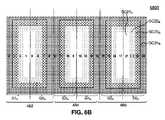
図6Aから6Dは、3Dメモリデバイスの階段構造領域680A及び680Bのそれぞれにおける第1の階段構造の上に第2の階段構造を形成した後の、3Dメモリデバイスの階段構造領域680A及び680Bの上面図のいくつかの実施形態を示す(例えば、第2の階段構造を第1の階段構造の上に重ねる)。図6A及び6Bは3Dメモリデバイスの階段構造領域680A及び680Bの上面図を示し、図6C及び6Dは、3Dメモリデバイスの階段構造領域680A及び680Bの断面図を示す。第2の階段構造の形成は、3Dメモリデバイス(図5A及び5Bに示されるような3Dメモリデバイス580A及び580B)の上面の上に形成され、パターニングされたマスク積層体(図示されない)を用いたエッチ-トリムプロセスを繰り返し適用することを含む。いくつかの実施形態において、マスク積層体は、フォトレジストまたは炭素ベースのポリマー材料を含みうる。マスク積層体は、第1の方向(例えばx方向)の階段構造領域580A及び580Bのそれぞれの第1の部分(例えば、図5A及び5Bに示されるようなS1A及びS1B)を露出する。いくつかの実施形態において、エッチ-トリムプロセスは、M個のレベルの連続するSC層を除去することであり、したがって、エッチングプロセスの繰り返しまたは任意の他のウェット/ドライエッチングプロセスを含みうる。マスク積層体は、階段構造領域580A及び580Bのそれぞれの第2の部分(例えば図5A及び5Bに示されるようなS2A及びS2B)を露出するためにトリム可能であり、続いて連続するSC層のM個のレベルを除去するためにエッチングプロセスが行われうる。いくつかの実施形態において、エッチ-トリムプロセスは、SC層の全ての上面(例えば図6Cに示されるようなSC1A、SC2A、・・・SC24A及び図6Dに示されるようなSC1B、SC2B、・・・SC24B)が電気的接続のために露出されるまで繰り返される。第2の階段構造の形成後、階段構造領域に2×N×M個(例えば、図6Aから6Dに示されるように2*4*3=24個)のステップを有する階段構造が形成される。そして、N個のサブ階段構造のそれぞれは、2×M個のステップを含む。いくつかの実施形態において、第1の階段構造を形成するためのエッチ-トリムプロセスは、第1のマスク積層体の横方向縁境界からマスク積層体の中央に向かう方向に、内側に向かって実行されうる(例えば図1から3及び図4A)。そして、各サブ階段構造領域(例えばサブ階段構造領域481、483及び485)の階段構造の最も上の層積層体は、サブ階段構造領域の中央部に位置する。いくつかの実施形態において、エッチ-トリムプロセスは、第1のマスク積層体の中央からマスク積層体の横方向の縁境界に向かう方向に、外側に向かって実行されうる(例えば図4B)。そして、各サブ階段領域(例えばサブ階段領域482、484、486)の階段構造の最も上の層積層体は、サブ階段構造領域の境界に位置する。Figures 6A-6D show top surfaces of
本開示の実施形態はさらに、3Dメモリデバイスの階段構造を形成するための方法を提供する。図7は、いくつかの実施形態に従う3Dメモリデバイスを形成するための例示的な方法700を示す。方法700の実施は、図1から6Dに示されたメモリデバイス構造を形成するために使用可能である。方法700に示された動作は網羅的ではなく、その他の動作が、図示された動作のいずれかの前、後、または間に実行されうることは理解されるべきである。いくつかの実施形態において、例示的な方法700のいくつかの動作が省略され、または単純化のために本明細書では説明されない他の動作を含みうる。いくつかの実施形態において、方法700の動作は、異なる順序で実施され、及び/または変動しうる。 Embodiments of the present disclosure further provide a method for forming a staircase structure for a 3D memory device. FIG. 7 shows an
動作710において、基板が3Dメモリデバイスを形成するために提供される。基板は、3次元メモリ構造を形成するための任意の適切な材料を含みうる。例えば、基板はシリコン、シリコンゲルマニウム、炭化シリコン、SOI、GOI、ガラス、窒化ガリウム、ガリウムヒ素、プラスチックシート及び/またはその他の適切なIII-V化合物を含みうる。 At
動作720において、交互層積層体が基板上に成膜される。交互層積層体の各層積層体はSC層を表す。SC層は、第1の材料層及び第2の材料層を有する誘電体層の対を含みうる。いくつかの実施形態において、第1の材料層は絶縁層であり、第2の材料層は犠牲層であり、またはその逆でありうる。いくつかの実施形態において、第1の材料層は絶縁層であり、第2の材料層は導体材料層であり、またはその逆でありうる。犠牲層は、窒化シリコン、多結晶シリコン、多結晶ゲルマニウム、多結晶ゲルマニウム-シリコン、任意の他の適切な材料及び/またはそれらの組み合わせなどの材料を含みうる。絶縁層は、酸化シリコン、酸化アルミニウムまたはその他の適切な材料などの材料を含みうる。導体材料層は、タングステン、窒化チタン、窒化タンタル、窒化タングステン、任意の他の適切な材料及び/またはそれらの組み合わせなどの材料を含みうる。絶縁、犠牲及び導体材料層のそれぞれは、CVD、PVD、ALDまたはそれらの任意の組み合わせを含むがそれらに限定しない1つまたは複数の薄膜成膜プロセスによって成膜された材料を含みうる。複数のSC層の例は、図1において上述したような交互層102および104でありうる。 At
動作730において、マスク積層体が、積層記憶領域及び複数の階段構造領域をSC層の上面にパターニングするために使用される。階段構造領域のそれぞれは、積層記憶領域に隣接する。いくつかの実施形態において、第1の複数の階段構造領域は、積層記憶領域によって水平方向に、第2の複数の階段構造領域から分離される。いくつかの実施形態において、積層記憶領域及び複数の階段構造領域は、リソグラフィを含む複数のプロセスを用いてマスク積層体によってパターニングされる。いくつかの実施形態において、マスク積層体は、フォトレジストまたは炭素ベースのポリマー材料を含みうる。積層記憶領域及び複数のSC層の例は、図4Aにおいて上述したように領域460、480A及び490Aでありうる。いくつかの実施形態において、第1のマスク積層体は、リソグラフィプロセスを用いて交互層積層体の上にN個のサブ階段構造領域を含む階段構造領域を画定するためにパターニングされ、Nは1より大きい。In
動作740において、第1の階段構造が階段構造領域のそれぞれに形成される。第1の階段構造は、マスク積層体を用いてエッチ-トリムプロセスを繰り返し実行することによって、階段構造領域のそれぞれに形成されうる。エッチ-トリムプロセスは、エッチングプロセス及びトリミングプロセスを含む。いくつかの実施形態において、エッチングプロセスはSC層の一部をエッチングする。いくつかの実施形態において、エッチングプロセスは、複数のSC層の一部をエッチングする。いくつかの実施形態において、1つまたは複数のエッチャントがエッチングプロセスで用いられ、エッチャントのそれぞれは、第2の材料層よりもずっと高いエッチングレートで第1の材料層をエッチングし、またはその逆である(例えば、第1の材料層と第2の材料層との間に高いエッチング選択性がある)。いくつかの実施形態において、エッチングプロセスは、第1の材料層と第2の材料層との間の高いエッチング選択性のために、SC層のエッチングを精度良く制御可能である。トリミングプロセスは、マスク積層体の適切なエッチング(例えば等方性ドライエッチングまたはウェットエッチング)を含み、基板の表面に対して平行な方向に生じる。トリミングされるマスク積層体の量は、第1の階段構造の横方向寸法に直接相関しうる。エッチ-トリムプロセスを繰り返した後、得られる第1の階段構造は、M個のステップを含み、M個のステップのそれぞれは1つのレベルである。いくつかの実施形態において、Mは1よりも大きい。いくつかの実施形態において、Mは2、3、4、5または6である。いくつかの実施形態において、Mは4である(図5Aから5Dに示されるように)。エッチ-トリムプロセスは、図1から3の説明を参照可能である。第1の階段構造の形成は、図4Aから5Dの説明を参照可能である。 At
動作750において、第2の階段構造が第1の階段構造の上に形成される。いくつかの実施形態において、マスク積層体が、階段構造領域の第1の部分(例えばSC1A及びSC1B)を露出し、階段構造領域の残りの部分を覆うためにパターニングされる。いくつかの実施形態において、マスク積層体は積層記憶領域を覆う。いくつかの実施形態において、マスク積層体はリソグラフィプロセスによってパターニングされる。エッチングプロセスは、エッチ-トリムプロセスで使用されるエッチングプロセスと同様に、露出された第1の階段構造領域からM個のレベルのSC層を除去するために適用される。マスク積層体は、エッチングプロセス後に除去される。結果として、第1の複数の階段構造領域における最も上のSC層(例えば図6Cに示されるようにSC4A)は、第2の複数の階段構造領域における最も上のSC層(例えば図6Cに示されるようにSC4B)よりも低いMのレベルである。マスク積層体を用いた、エッチ-トリムプロセスの繰り返しは、SC層の全ての上面(例えば図6Cに示されるようなSC1A、SC2A、・・・SC24A及び図6Dに示されるようなSC1B、SC2B、・・・SC24B)が電気的接続のために露出されるまで実行されうる。いくつかの実施形態において、エッチ-トリムプロセスは、トリミングプロセス及び、SC層のM個をエッチングするエッチングプロセスを含む。第1の階段構造の上に第2の階段構造を形成することは、図6Aから6Dの説明を参照できる。At
段階760において、半導体チャネルを含む記憶構造が、積層記憶領域に形成される。さらなるプロセスステップは、3Dメモリデバイスの階段構造領域のそれぞれに相互接続構造を形成することを含みうる。いくつかの実施形態において、半導体チャネルは、積層記憶領域においてSC層を通って形成され、延在される。3Dメモリデバイスのワード線は、SC層のそれぞれの犠牲材料層を導体層と置き換えることによって形成される。階段構造領域における階段構造は、3Dメモリデバイスの各ワード線の一部を露出し、これによって相互接続構造(例えばVIA構造)が半導体チャネルのそれぞれを制御するための各ワード線のファンアウトを提供可能になる。 At
本明細書で説明された様々な実施形態は、3Dメモリデバイスの階段構造及びその製造方法に関する。例示的な製造方法は、基板の上に配置された複数の誘電体層の対を含む交互層積層体を形成する段階と、交互層積層体の上に第1のマスク積層体を形成する段階と、交互層積層体の上のN個のサブ階段構造を含む階段構造を画定するために第1のマスク積層体をパターニングする段階と、階段構造領域の上に第1の階段構造を形成する段階であって、第1の階段構造が階段構造領域のそれぞれにおいてM個のステップを有する、段階と、第1の階段構造の上に第2の階段構造を形成する段階と、を含む。N及びMはともに1より大きく、第2の階段構造は、階段構造領域において2*N*M個のステップを有する。いくつかの実施形態において、本方法はさらに、基板の上の積層記憶領域に複数の垂直半導体チャネルを形成する段階を含み、階段構造領域のそれぞれは、積層記憶領域に隣接する。いくつかの実施形態において、3Dメモリデバイスは、基板上に配置された交互層積層体と、複数の垂直半導体チャネルを含む記憶構造と、記憶構造に隣接する複数の階段構造領域と、交互層積層体の複数の層積層体の一部を露出するために、階段構造領域のそれぞれに設けられた階段構造と、を含む。いくつかの実施形態において、階段構造は、N個のサブ階段構造領域を含み、Nは1より大きい。いくつかの実施形態において、N個のサブ階段構造領域のそれぞれは、2*M個のステップを含み、Mは1より大きい。開示された構造及び方法は、3Dメモリデバイスの製造の複雑さ及び製造コストを低減することを含むがそれに限定しない多数の利益を提供する。 Various embodiments described herein relate to staircase structures for 3D memory devices and methods of manufacturing the same. An exemplary fabrication method includes forming an alternating layer stack including a plurality of pairs of dielectric layers disposed over a substrate, and forming a first mask stack over the alternating layer stack. and patterning a first mask stack to define a stair structure including N sub-stair structures over the alternating layer stack; and forming the first stair structure over the stair structure region. steps, wherein the first stair structure has M steps in each of the stair structure regions; and forming a second stair structure over the first stair structure. Both N and M are greater than 1 and the second stair structure has 2*N*M steps in the stair structure area. In some embodiments, the method further includes forming a plurality of vertical semiconductor channels in a stacked storage region over the substrate, each of the step structure regions adjacent to the stacked storage region. In some embodiments, a 3D memory device includes an alternating layer stack disposed on a substrate, a storage structure including a plurality of vertical semiconductor channels, a plurality of stepped regions adjacent to the storage structure, and an alternating layer stack. a stepped structure provided in each of the stepped structure regions to expose a portion of the plurality of layer stacks of the body. In some embodiments, the stair structure includes N sub-stair structure regions, where N is greater than one. In some embodiments, each of the N sub-step structure regions includes 2*M steps, where M is greater than one. The disclosed structures and methods provide numerous benefits including, but not limited to, reducing the complexity and cost of manufacturing 3D memory devices.
特定の実施形態の前述の説明は、当業者の知識を適用することによって、容易に他者が、そのような特定の実施形態を、不要な実験を行うことなく、本開示の一般的な概念を逸脱することなく改変及び/または様々な用途に適合することが可能である、本開示の一般的な本質を完全に明らかにする。したがって、そのような適合及び改変は、本明細書で示された教示及びガイダンスに基づき、開示された実施形態の等価物の意味及び範囲内にあることが意図される。本明細書の用語や語句は、説明のためのものであり、限定の目的ではなく、本明細書の用語や語句は、当業者が教示やガイダンスに照らして解釈されるものであることは理解されるべきである。 The foregoing descriptions of specific embodiments are intended to enable others, by applying the knowledge of those skilled in the art, to readily render such specific embodiments to the general concept of the present disclosure without undue experimentation. A full disclosure of the general nature of this disclosure, which may be modified and/or adapted for various applications without departing from the scope of the present invention. Therefore, such adaptations and modifications are intended to be within the meaning and range of equivalents of the disclosed embodiments, based on the teaching and guidance presented herein. It is understood that the terms and phrases herein are for the purpose of description and not for the purpose of limitation, and that the terms and phrases herein are to be interpreted in light of the teachings and guidance of those skilled in the art. It should be.
本開示の実施形態は、その特定の機能及び関係性の実施を示す機能的な構成ブロックを用いて前述された。これらの機能的な構成ブロックの境界は、説明の便宜上、本明細書では任意に定義されている。特定の機能とその関係性が適切に実施される限り、代替的な境界も定義されうる。 Embodiments of the present disclosure have been described above using functional building blocks to illustrate the implementation of certain functions and relationships thereof. The boundaries of these functional building blocks have been arbitrarily defined herein for the convenience of the description. Alternate boundaries can be defined so long as the specified functions and relationships thereof are appropriately performed.
概要及び要約は、発明者が考えている本開示の1つ以上ではあるが全てではない例示的な実施形態を示しうるものであり、そのため、本開示及び添付の特許請求の範囲をいかなる方法でも限定することを意図されていない。 The summary and abstract may present one or more, but not all, exemplary embodiments of the disclosure contemplated by the inventor, and thus may be interpreted in any way to interpret the disclosure and the appended claims. Not intended to be limiting.
本開示の幅及び範囲は、上述の例示的な実施形態のいずれかによって限定されるべきではなく、以下の特許請求の範囲及びその均等物のみに従って定義されるべきである。 The breadth and scope of the present disclosure should not be limited by any of the above-described exemplary embodiments, but should be defined only in accordance with the following claims and their equivalents.
100 構造
101、103 SC層の領域
102、106、110、・・・ 第1の材料層
104、108、112、・・・ 第2の材料層
153 マスク積層体
160 基板
194 第1の材料層
196 第2の材料層
200 階段構造
294、296 層
300A、300B 階段構造
353 マスク積層体
400A、400B 3Dメモリデバイス
453A、453B マスク層
460 積層記憶構造領域
470 スリット
480、490 階段構造
481~486 サブ階段構造領域
580A、580B 階段構造領域
680A、680B 階段構造領域
SC1A~SC24A、SC1B~SC24B ステップ100
Claims (20)
Translated fromJapanese基板の上に配置された複数の誘電体層の対を含む交互層積層体を形成する段階と、
前記交互層積層体の上に第1のマスク積層体を形成する段階と、
前記交互層積層体の上にN個のサブ階段構造領域を含む階段構造領域を画定するために前記第1のマスク積層体をパターニングする段階であって、Nが1より大きい、前記第1のマスク積層体をパターニングする段階と、
前記階段構造領域の上に第1の階段構造を形成する段階であって、前記第1の階段構造が前記階段構造領域のそれぞれにおいてM個のステップを有し、Mが1より大きい、第1の階段構造を形成する段階と、
前記第1の階段構造の上に第2の階段構造を形成する段階と、を含み、
前記第2の階段構造が、前記階段構造領域において2*N*M個のステップを有し、
前記階段構造のステップのそれぞれが異なる高さにある、方法。A method for forming a 3D memory device, comprising:
forming an alternating layer stack including a plurality of pairs of dielectric layers disposed over a substrate;
forming a first mask stack over the alternating layer stack;
patterning the first mask stack to define a staircase structure region including N sub-step structure regions on the alternating layer stack, wherein N is greater than 1; patterning the mask stack;
forming a first staircase structure over the staircase structure region, the first staircase structure having M steps in each of the staircase structure regions, M being greater than 1; forming a staircase structure of
forming a second stair structure over the first stair structure;
the second staircase structure has 2*N*M steps in the staircase structure region;
A method, wherein each of the steps of said staircase structure are at different heights .
前記第1のマスク積層体を用いて最も上の誘電体層の対の一部を除去する段階と、
前記第1のマスク積層体をトリミングする段階と、
M個のステップが形成されるまで、前記除去及び前記トリミングを順に繰り返すことによって、前記第1の階段構造を形成する段階と、を含む、請求項1に記載の方法。Forming the first staircase structure comprises:
removing a portion of a top dielectric layer pair using the first mask stack;
trimming the first mask stack;
forming the first staircase structure by sequentially repeating the removal and the trimming until M steps are formed.
第2のマスク積層体を用いて誘電体層の対のM個の層の一部を除去する段階と、
前記第2のマスク積層体をトリミングする段階と、
2*N*M個のステップが形成されるまで、前記除去及び前記トリミングを順に繰り返すことによって、前記第2の階段構造を形成する段階と、を含む、請求項1に記載の方法。Forming the second staircase structure comprises:
removing a portion of the M layers of the pair of dielectric layers using a second mask stack;
trimming the second mask stack;
forming the second staircase structure by sequentially repeating the removal and the trimming until 2*N*M steps are formed.
基板上に配置された交互層積層体と、
複数の垂直半導体チャネルを含む記憶構造と、
前記記憶構造に隣接する複数の階段構造領域と、
前記交互層積層体の複数の層積層体の一部を露出するために前記階段構造領域のそれぞれに配置された階段構造と、を含み、
前記階段構造がN個のサブ階段構造領域を含み、
Nが1より大きく、
N個のサブ階段構造領域のそれぞれが2*M個のステップを含み、
Mが1より大きく、
前記階段構造のステップのそれぞれが異なる高さにある、3Dメモリデバイス。A 3D memory device,
an alternating layer stack disposed on a substrate;
a storage structure including a plurality of vertical semiconductor channels;
a plurality of staircase structure regions adjacent to the storage structure;
a stepped structure positioned in each of the stepped structure regions to expose a portion of the plurality of layer stacks of the alternating layer stack;
The staircase structure includes N sub-staircase structure regions,
N is greater than 1,
each of the N sub-staircase structure regions includes 2*M steps;
M isgreater than 1,
A 3D memory device, wherein each step of the staircase structure is at a different height .
Priority Applications (1)
| Application Number | Priority Date | Filing Date | Title |
|---|---|---|---|
| JP2022195724AJP7729801B2 (en) | 2019-01-31 | 2022-12-07 | Formation of staircase structures in three-dimensional memory devices |
Applications Claiming Priority (1)
| Application Number | Priority Date | Filing Date | Title |
|---|---|---|---|
| PCT/CN2019/074073WO2020154997A1 (en) | 2019-01-31 | 2019-01-31 | Staircase formation in three-dimensional memory device |
Related Child Applications (1)
| Application Number | Title | Priority Date | Filing Date |
|---|---|---|---|
| JP2022195724ADivisionJP7729801B2 (en) | 2019-01-31 | 2022-12-07 | Formation of staircase structures in three-dimensional memory devices |
Publications (2)
| Publication Number | Publication Date |
|---|---|
| JP2022509276A JP2022509276A (en) | 2022-01-20 |
| JP7192121B2true JP7192121B2 (en) | 2022-12-19 |
Family
ID=67017304
Family Applications (2)
| Application Number | Title | Priority Date | Filing Date |
|---|---|---|---|
| JP2021530980AActiveJP7192121B2 (en) | 2019-01-31 | 2019-01-31 | Formation of staircase structures in three-dimensional memory devices |
| JP2022195724AActiveJP7729801B2 (en) | 2019-01-31 | 2022-12-07 | Formation of staircase structures in three-dimensional memory devices |
Family Applications After (1)
| Application Number | Title | Priority Date | Filing Date |
|---|---|---|---|
| JP2022195724AActiveJP7729801B2 (en) | 2019-01-31 | 2022-12-07 | Formation of staircase structures in three-dimensional memory devices |
Country Status (7)
| Country | Link |
|---|---|
| US (5) | US10896844B2 (en) |
| EP (2) | EP3853899B1 (en) |
| JP (2) | JP7192121B2 (en) |
| KR (1) | KR102611731B1 (en) |
| CN (2) | CN109952644A (en) |
| TW (1) | TWI707457B (en) |
| WO (1) | WO2020154997A1 (en) |
Families Citing this family (15)
| Publication number | Priority date | Publication date | Assignee | Title |
|---|---|---|---|---|
| WO2020154997A1 (en) | 2019-01-31 | 2020-08-06 | Yangtze Memory Technologies Co., Ltd. | Staircase formation in three-dimensional memory device |
| CN113678254A (en)* | 2019-04-04 | 2021-11-19 | 三星电子株式会社 | Three-dimensional flash memory and method of manufacturing the same |
| KR102668097B1 (en)* | 2019-07-24 | 2024-05-23 | 에스케이하이닉스 주식회사 | Semiconductor memory device and manufacturing method thereof |
| CN110534527B (en)* | 2019-09-06 | 2022-07-12 | 长江存储科技有限责任公司 | Three-dimensional memory and method of forming the same |
| US11133252B2 (en)* | 2020-02-05 | 2021-09-28 | Sandisk Technologies Llc | Three-dimensional memory device containing horizontal and vertical word line interconnections and methods of forming the same |
| WO2021189190A1 (en)* | 2020-03-23 | 2021-09-30 | Yangtze Memory Technologies Co., Ltd. | Staircase structure in three-dimensional memory device and method for forming the same |
| KR102674073B1 (en)* | 2020-03-23 | 2024-06-10 | 양쯔 메모리 테크놀로지스 씨오., 엘티디. | Staircase structure of 3D memory device and method for forming the same |
| CN113097215B (en)* | 2020-06-11 | 2021-12-07 | 长江存储科技有限责任公司 | Three-dimensional memory structure and preparation method thereof |
| CN112185974B (en)* | 2020-09-11 | 2024-06-07 | 长江存储科技有限责任公司 | Manufacturing method of 3D NAND memory device and 3D NAND memory device |
| CN112614856B (en)* | 2020-12-17 | 2024-04-23 | 长江存储科技有限责任公司 | Semiconductor device, method for manufacturing semiconductor device, and mask system |
| JP2023039082A (en)* | 2021-09-08 | 2023-03-20 | キオクシア株式会社 | semiconductor storage device |
| US20240015961A1 (en)* | 2022-07-11 | 2024-01-11 | Yangtze Memory Technologies Co., Ltd. | Control Gate Structures in Three-Dimensional Memory Devices and Methods for Forming the Same |
| US20240032288A1 (en)* | 2022-07-19 | 2024-01-25 | Yangtze Memory Technologies Co., Ltd. | Three-dimensional memory device, memory system, and methods for forming the same |
| US12315733B2 (en)* | 2023-02-07 | 2025-05-27 | Applied Materials, Inc. | Enhanced etch selectivity using halides |
| US20250194090A1 (en)* | 2023-12-06 | 2025-06-12 | Micron Technology, Inc. | Integrated Circuitry, Memory Circuitry, And Method Of Forming Integrated Circuitry |
Citations (5)
| Publication number | Priority date | Publication date | Assignee | Title |
|---|---|---|---|---|
| US20170317088A1 (en) | 2016-05-02 | 2017-11-02 | SK Hynix Inc. | Semiconductor device and method of manufacturing the same |
| US20170373088A1 (en) | 2016-06-27 | 2017-12-28 | SK Hynix Inc. | Semiconductor device and method of manufacturing the same |
| US20180301372A1 (en) | 2017-04-13 | 2018-10-18 | SK Hynix Inc. | Method of manufacturing a semiconductor device |
| JP2020113766A (en) | 2019-01-15 | 2020-07-27 | 三星電子株式会社Samsung Electronics Co.,Ltd. | Three-dimensional semiconductor memory device and method of manufacturing the same |
| JP2020126928A (en) | 2019-02-05 | 2020-08-20 | キオクシア株式会社 | Semiconductor storage device and method for manufacturing the same |
Family Cites Families (50)
| Publication number | Priority date | Publication date | Assignee | Title |
|---|---|---|---|---|
| US7511826B2 (en)* | 2006-02-27 | 2009-03-31 | Asml Holding N.V. | Symmetrical illumination forming system and method |
| US7795149B2 (en)* | 2006-06-01 | 2010-09-14 | Micron Technology, Inc. | Masking techniques and contact imprint reticles for dense semiconductor fabrication |
| JP5091526B2 (en) | 2007-04-06 | 2012-12-05 | 株式会社東芝 | Semiconductor memory device and manufacturing method thereof |
| JP5330017B2 (en) | 2009-02-17 | 2013-10-30 | 株式会社東芝 | Nonvolatile semiconductor memory device and manufacturing method thereof |
| US9892972B2 (en)* | 2009-10-12 | 2018-02-13 | Monolithic 3D Inc. | 3D semiconductor device and structure |
| KR101787041B1 (en)* | 2010-11-17 | 2017-10-18 | 삼성전자주식회사 | Methods for forming semiconductor devices having etch stopping layers, and methods for fabricating semiconductor devices |
| KR101744127B1 (en)* | 2010-11-17 | 2017-06-08 | 삼성전자주식회사 | Semiconductor devices and methods for fabricating the same |
| JP2012119478A (en) | 2010-11-30 | 2012-06-21 | Toshiba Corp | Semiconductor memory device and fabricating method thereof |
| US8329051B2 (en)* | 2010-12-14 | 2012-12-11 | Lam Research Corporation | Method for forming stair-step structures |
| US8530350B2 (en)* | 2011-06-02 | 2013-09-10 | Micron Technology, Inc. | Apparatuses including stair-step structures and methods of forming the same |
| KR20130066950A (en)* | 2011-12-13 | 2013-06-21 | 에스케이하이닉스 주식회사 | Three dimension non-volatile memory device, memory system comprising the same and method of manufacturing the same |
| KR20130072522A (en)* | 2011-12-22 | 2013-07-02 | 에스케이하이닉스 주식회사 | Three dimension non-volatile memory device and method for manufacturing the same |
| KR20130072523A (en)* | 2011-12-22 | 2013-07-02 | 에스케이하이닉스 주식회사 | Three dimension non-volatile memory device and method of manufacturing the same |
| KR101981996B1 (en)* | 2012-06-22 | 2019-05-27 | 에스케이하이닉스 주식회사 | Semiconductor device and method of manufacturing the same |
| US8928149B2 (en)* | 2013-03-12 | 2015-01-06 | Macronix International Co., Ltd. | Interlayer conductor and method for forming |
| US9099538B2 (en)* | 2013-09-17 | 2015-08-04 | Macronix International Co., Ltd. | Conductor with a plurality of vertical extensions for a 3D device |
| KR102183713B1 (en)* | 2014-02-13 | 2020-11-26 | 삼성전자주식회사 | Staircase Connection Structure Of Three-Dimensional Semiconductor Device And Method Of Forming The Same |
| US9362338B2 (en)* | 2014-03-03 | 2016-06-07 | Sandisk Technologies Inc. | Vertical thin film transistors in non-volatile storage systems |
| KR20150139255A (en)* | 2014-06-03 | 2015-12-11 | 에스케이하이닉스 주식회사 | Semiconductor device and method of manufacturing the same |
| US9601502B2 (en)* | 2014-08-26 | 2017-03-21 | Sandisk Technologies Llc | Multiheight contact via structures for a multilevel interconnect structure |
| US9401309B2 (en)* | 2014-08-26 | 2016-07-26 | Sandisk Technologies Llc | Multiheight contact via structures for a multilevel interconnect structure |
| US9478546B2 (en)* | 2014-10-16 | 2016-10-25 | Macronix International Co., Ltd. | LC module layout arrangement for contact opening etch windows |
| US9502429B2 (en)* | 2014-11-26 | 2016-11-22 | Sandisk Technologies Llc | Set of stepped surfaces formation for a multilevel interconnect structure |
| US9530781B2 (en)* | 2014-12-22 | 2016-12-27 | Sandisk Technologies Llc | Three dimensional NAND memory having improved connection between source line and in-hole channel material as well as reduced damage to in-hole layers |
| US9741731B2 (en)* | 2014-12-22 | 2017-08-22 | Macronix International Co., Ltd. | Three dimensional stacked semiconductor structure |
| TWI559370B (en)* | 2015-01-15 | 2016-11-21 | 力晶科技股份有限公司 | Method for fabricating semiconductor structure |
| KR102287275B1 (en)* | 2015-04-17 | 2021-08-09 | 에스케이하이닉스 주식회사 | Semiconductor device and method of manufacturing the same |
| KR20160128731A (en)* | 2015-04-29 | 2016-11-08 | 에스케이하이닉스 주식회사 | Three dimension semiconductor device |
| US9627498B2 (en)* | 2015-05-20 | 2017-04-18 | Macronix International Co., Ltd. | Contact structure for thin film semiconductor |
| KR20170014757A (en) | 2015-07-31 | 2017-02-08 | 에스케이하이닉스 주식회사 | Semiconductor device and manufacturing method of the same |
| US10381361B2 (en)* | 2015-09-10 | 2019-08-13 | Samsung Electronics Co., Ltd. | Method for manufacturing semiconductor device |
| KR102424720B1 (en)* | 2015-10-22 | 2022-07-25 | 삼성전자주식회사 | Vertical memory devices and methods of manufacturing the same |
| KR102568886B1 (en)* | 2015-11-16 | 2023-08-22 | 에스케이하이닉스 주식회사 | Semiconductor device and manufacturing method of the same |
| KR102508897B1 (en)* | 2015-12-17 | 2023-03-10 | 삼성전자주식회사 | A vertical memory device and methods of forming the same |
| US10049744B2 (en)* | 2016-01-08 | 2018-08-14 | Samsung Electronics Co., Ltd. | Three-dimensional (3D) semiconductor memory devices and methods of manufacturing the same |
| US9905514B2 (en)* | 2016-04-11 | 2018-02-27 | Micron Technology, Inc. | Semiconductor device structures including staircase structures, and related methods and electronic systems |
| KR20180007811A (en)* | 2016-07-14 | 2018-01-24 | 삼성전자주식회사 | Vertical memory devices |
| JP2018049968A (en)* | 2016-09-23 | 2018-03-29 | 東芝メモリ株式会社 | Integrated circuit device and manufacturing method of the same |
| US10134757B2 (en)* | 2016-11-07 | 2018-11-20 | Asm Ip Holding B.V. | Method of processing a substrate and a device manufactured by using the method |
| US10340281B2 (en) | 2017-03-14 | 2019-07-02 | Macronix International Co., Ltd. | Three-dimensional semiconductor device and method of manufacturing the same |
| TWI630709B (en)* | 2017-03-14 | 2018-07-21 | 旺宏電子股份有限公司 | Three-dimensional semiconductor device and method of manufacturing the same |
| JP6674406B2 (en)* | 2017-03-23 | 2020-04-01 | キオクシア株式会社 | Semiconductor device and manufacturing method thereof |
| TWI656601B (en)* | 2017-03-23 | 2019-04-11 | 旺宏電子股份有限公司 | Asymmetric stair structure and method for fabricating the same |
| US10847529B2 (en)* | 2017-04-13 | 2020-11-24 | Asm Ip Holding B.V. | Substrate processing method and device manufactured by the same |
| US10651087B2 (en) | 2017-08-31 | 2020-05-12 | Yangtze Memory Technologies Co., Ltd. | Method for forming three-dimensional integrated wiring structure and semiconductor structure thereof |
| US10474027B2 (en)* | 2017-11-13 | 2019-11-12 | Macronix International Co., Ltd. | Method for forming an aligned mask |
| US11342351B2 (en)* | 2018-01-10 | 2022-05-24 | Samsung Electronics Co., Ltd. | Three-dimensional semiconductor device |
| KR102639721B1 (en)* | 2018-04-13 | 2024-02-26 | 삼성전자주식회사 | Three-dimensional semiconductor memory devices |
| KR102563689B1 (en)* | 2018-05-18 | 2023-08-03 | 양쯔 메모리 테크놀로지스 씨오., 엘티디. | Step Formation in 3D Memory Devices |
| WO2020154997A1 (en) | 2019-01-31 | 2020-08-06 | Yangtze Memory Technologies Co., Ltd. | Staircase formation in three-dimensional memory device |
- 2019
- 2019-01-31WOPCT/CN2019/074073patent/WO2020154997A1/ennot_activeCeased
- 2019-01-31JPJP2021530980Apatent/JP7192121B2/enactiveActive
- 2019-01-31CNCN201980000263.3Apatent/CN109952644A/enactivePending
- 2019-01-31EPEP19913904.9Apatent/EP3853899B1/enactiveActive
- 2019-01-31KRKR1020217014412Apatent/KR102611731B1/enactiveActive
- 2019-01-31CNCN202111451410.4Apatent/CN114141781A/enactivePending
- 2019-01-31EPEP25153588.6Apatent/EP4521879A3/enactivePending
- 2019-03-12TWTW108108221Apatent/TWI707457B/enactive
- 2019-05-24USUS16/422,464patent/US10896844B2/enactiveActive
- 2020
- 2020-11-24USUS17/103,423patent/US11361988B2/enactiveActive
- 2021
- 2021-05-12USUS17/318,589patent/US11545388B2/enactiveActive
- 2022
- 2022-12-05USUS18/074,851patent/US11961760B2/enactiveActive
- 2022-12-07JPJP2022195724Apatent/JP7729801B2/enactiveActive
- 2024
- 2024-01-10USUS18/408,950patent/US12406879B2/enactiveActive
Patent Citations (5)
| Publication number | Priority date | Publication date | Assignee | Title |
|---|---|---|---|---|
| US20170317088A1 (en) | 2016-05-02 | 2017-11-02 | SK Hynix Inc. | Semiconductor device and method of manufacturing the same |
| US20170373088A1 (en) | 2016-06-27 | 2017-12-28 | SK Hynix Inc. | Semiconductor device and method of manufacturing the same |
| US20180301372A1 (en) | 2017-04-13 | 2018-10-18 | SK Hynix Inc. | Method of manufacturing a semiconductor device |
| JP2020113766A (en) | 2019-01-15 | 2020-07-27 | 三星電子株式会社Samsung Electronics Co.,Ltd. | Three-dimensional semiconductor memory device and method of manufacturing the same |
| JP2020126928A (en) | 2019-02-05 | 2020-08-20 | キオクシア株式会社 | Semiconductor storage device and method for manufacturing the same |
Also Published As
| Publication number | Publication date |
|---|---|
| US11961760B2 (en) | 2024-04-16 |
| EP4521879A2 (en) | 2025-03-12 |
| WO2020154997A1 (en) | 2020-08-06 |
| EP3853899A1 (en) | 2021-07-28 |
| KR102611731B1 (en) | 2023-12-07 |
| US11545388B2 (en) | 2023-01-03 |
| TWI707457B (en) | 2020-10-11 |
| US10896844B2 (en) | 2021-01-19 |
| US11361988B2 (en) | 2022-06-14 |
| TW202030871A (en) | 2020-08-16 |
| JP7729801B2 (en) | 2025-08-26 |
| US20240145296A1 (en) | 2024-05-02 |
| US20200251381A1 (en) | 2020-08-06 |
| CN114141781A (en) | 2022-03-04 |
| US20230102588A1 (en) | 2023-03-30 |
| JP2022509276A (en) | 2022-01-20 |
| EP3853899B1 (en) | 2025-01-29 |
| US12406879B2 (en) | 2025-09-02 |
| KR20210061452A (en) | 2021-05-27 |
| JP2023029357A (en) | 2023-03-03 |
| US20210098288A1 (en) | 2021-04-01 |
| US20210265203A1 (en) | 2021-08-26 |
| CN109952644A (en) | 2019-06-28 |
| EP4521879A3 (en) | 2025-06-04 |
| EP3853899A4 (en) | 2022-05-11 |
Similar Documents
| Publication | Publication Date | Title |
|---|---|---|
| JP7192121B2 (en) | Formation of staircase structures in three-dimensional memory devices | |
| US11997851B2 (en) | Staircase formation in three-dimensional memory device | |
| US11114439B2 (en) | Multi-division 3D NAND memory device | |
| US12137558B2 (en) | Staircase structure for memory device |
Legal Events
| Date | Code | Title | Description |
|---|---|---|---|
| A521 | Request for written amendment filed | Free format text:JAPANESE INTERMEDIATE CODE: A523 Effective date:20210528 | |
| A621 | Written request for application examination | Free format text:JAPANESE INTERMEDIATE CODE: A621 Effective date:20210528 | |
| A131 | Notification of reasons for refusal | Free format text:JAPANESE INTERMEDIATE CODE: A131 Effective date:20220606 | |
| A521 | Request for written amendment filed | Free format text:JAPANESE INTERMEDIATE CODE: A523 Effective date:20220905 | |
| TRDD | Decision of grant or rejection written | ||
| A01 | Written decision to grant a patent or to grant a registration (utility model) | Free format text:JAPANESE INTERMEDIATE CODE: A01 Effective date:20221107 | |
| A61 | First payment of annual fees (during grant procedure) | Free format text:JAPANESE INTERMEDIATE CODE: A61 Effective date:20221207 | |
| R150 | Certificate of patent or registration of utility model | Ref document number:7192121 Country of ref document:JP Free format text:JAPANESE INTERMEDIATE CODE: R150 |