JP7188230B2 - semiconductor equipment - Google Patents
semiconductor equipmentDownload PDFInfo
- Publication number
- JP7188230B2 JP7188230B2JP2019063289AJP2019063289AJP7188230B2JP 7188230 B2JP7188230 B2JP 7188230B2JP 2019063289 AJP2019063289 AJP 2019063289AJP 2019063289 AJP2019063289 AJP 2019063289AJP 7188230 B2JP7188230 B2JP 7188230B2
- Authority
- JP
- Japan
- Prior art keywords
- cell
- electrode
- region
- impurity concentration
- drift layer
- Prior art date
- Legal status (The legal status is an assumption and is not a legal conclusion. Google has not performed a legal analysis and makes no representation as to the accuracy of the status listed.)
- Active
Links
Images


Classifications
- H—ELECTRICITY
- H10—SEMICONDUCTOR DEVICES; ELECTRIC SOLID-STATE DEVICES NOT OTHERWISE PROVIDED FOR
- H10D—INORGANIC ELECTRIC SEMICONDUCTOR DEVICES
- H10D30/00—Field-effect transistors [FET]
- H10D30/60—Insulated-gate field-effect transistors [IGFET]
- H10D30/64—Double-diffused metal-oxide semiconductor [DMOS] FETs
- H10D30/66—Vertical DMOS [VDMOS] FETs
- H10D30/668—Vertical DMOS [VDMOS] FETs having trench gate electrodes, e.g. UMOS transistors
- H—ELECTRICITY
- H01—ELECTRIC ELEMENTS
- H01L—SEMICONDUCTOR DEVICES NOT COVERED BY CLASS H10
- H01L21/00—Processes or apparatus adapted for the manufacture or treatment of semiconductor or solid state devices or of parts thereof
- H01L21/02—Manufacture or treatment of semiconductor devices or of parts thereof
- H01L21/04—Manufacture or treatment of semiconductor devices or of parts thereof the devices having potential barriers, e.g. a PN junction, depletion layer or carrier concentration layer
- H01L21/18—Manufacture or treatment of semiconductor devices or of parts thereof the devices having potential barriers, e.g. a PN junction, depletion layer or carrier concentration layer the devices having semiconductor bodies comprising elements of Group IV of the Periodic Table or AIIIBV compounds with or without impurities, e.g. doping materials
- H01L21/28—Manufacture of electrodes on semiconductor bodies using processes or apparatus not provided for in groups H01L21/20 - H01L21/268
- H—ELECTRICITY
- H10—SEMICONDUCTOR DEVICES; ELECTRIC SOLID-STATE DEVICES NOT OTHERWISE PROVIDED FOR
- H10D—INORGANIC ELECTRIC SEMICONDUCTOR DEVICES
- H10D30/00—Field-effect transistors [FET]
- H10D30/60—Insulated-gate field-effect transistors [IGFET]
- H—ELECTRICITY
- H10—SEMICONDUCTOR DEVICES; ELECTRIC SOLID-STATE DEVICES NOT OTHERWISE PROVIDED FOR
- H10D—INORGANIC ELECTRIC SEMICONDUCTOR DEVICES
- H10D30/00—Field-effect transistors [FET]
- H10D30/60—Insulated-gate field-effect transistors [IGFET]
- H10D30/64—Double-diffused metal-oxide semiconductor [DMOS] FETs
- H10D30/66—Vertical DMOS [VDMOS] FETs
- H10D30/665—Vertical DMOS [VDMOS] FETs having edge termination structures
- H—ELECTRICITY
- H10—SEMICONDUCTOR DEVICES; ELECTRIC SOLID-STATE DEVICES NOT OTHERWISE PROVIDED FOR
- H10D—INORGANIC ELECTRIC SEMICONDUCTOR DEVICES
- H10D62/00—Semiconductor bodies, or regions thereof, of devices having potential barriers
- H10D62/10—Shapes, relative sizes or dispositions of the regions of the semiconductor bodies; Shapes of the semiconductor bodies
- H10D62/102—Constructional design considerations for preventing surface leakage or controlling electric field concentration
- H10D62/103—Constructional design considerations for preventing surface leakage or controlling electric field concentration for increasing or controlling the breakdown voltage of reverse-biased devices
- H10D62/104—Constructional design considerations for preventing surface leakage or controlling electric field concentration for increasing or controlling the breakdown voltage of reverse-biased devices having particular shapes of the bodies at or near reverse-biased junctions, e.g. having bevels or moats
- H—ELECTRICITY
- H10—SEMICONDUCTOR DEVICES; ELECTRIC SOLID-STATE DEVICES NOT OTHERWISE PROVIDED FOR
- H10D—INORGANIC ELECTRIC SEMICONDUCTOR DEVICES
- H10D62/00—Semiconductor bodies, or regions thereof, of devices having potential barriers
- H10D62/10—Shapes, relative sizes or dispositions of the regions of the semiconductor bodies; Shapes of the semiconductor bodies
- H10D62/102—Constructional design considerations for preventing surface leakage or controlling electric field concentration
- H10D62/103—Constructional design considerations for preventing surface leakage or controlling electric field concentration for increasing or controlling the breakdown voltage of reverse-biased devices
- H10D62/105—Constructional design considerations for preventing surface leakage or controlling electric field concentration for increasing or controlling the breakdown voltage of reverse-biased devices by having particular doping profiles, shapes or arrangements of PN junctions; by having supplementary regions, e.g. junction termination extension [JTE]
- H10D62/106—Constructional design considerations for preventing surface leakage or controlling electric field concentration for increasing or controlling the breakdown voltage of reverse-biased devices by having particular doping profiles, shapes or arrangements of PN junctions; by having supplementary regions, e.g. junction termination extension [JTE] having supplementary regions doped oppositely to or in rectifying contact with regions of the semiconductor bodies, e.g. guard rings with PN or Schottky junctions
- H—ELECTRICITY
- H10—SEMICONDUCTOR DEVICES; ELECTRIC SOLID-STATE DEVICES NOT OTHERWISE PROVIDED FOR
- H10D—INORGANIC ELECTRIC SEMICONDUCTOR DEVICES
- H10D62/00—Semiconductor bodies, or regions thereof, of devices having potential barriers
- H10D62/10—Shapes, relative sizes or dispositions of the regions of the semiconductor bodies; Shapes of the semiconductor bodies
- H10D62/17—Semiconductor regions connected to electrodes not carrying current to be rectified, amplified or switched, e.g. channel regions
- H10D62/393—Body regions of DMOS transistors or IGBTs
- H—ELECTRICITY
- H10—SEMICONDUCTOR DEVICES; ELECTRIC SOLID-STATE DEVICES NOT OTHERWISE PROVIDED FOR
- H10D—INORGANIC ELECTRIC SEMICONDUCTOR DEVICES
- H10D64/00—Electrodes of devices having potential barriers
- H10D64/20—Electrodes characterised by their shapes, relative sizes or dispositions
- H10D64/23—Electrodes carrying the current to be rectified, amplified, oscillated or switched, e.g. sources, drains, anodes or cathodes
- H10D64/251—Source or drain electrodes for field-effect devices
- H10D64/252—Source or drain electrodes for field-effect devices for vertical or pseudo-vertical devices
- H—ELECTRICITY
- H10—SEMICONDUCTOR DEVICES; ELECTRIC SOLID-STATE DEVICES NOT OTHERWISE PROVIDED FOR
- H10D—INORGANIC ELECTRIC SEMICONDUCTOR DEVICES
- H10D64/00—Electrodes of devices having potential barriers
- H10D64/60—Electrodes characterised by their materials
- H10D64/62—Electrodes ohmically coupled to a semiconductor
- H—ELECTRICITY
- H10—SEMICONDUCTOR DEVICES; ELECTRIC SOLID-STATE DEVICES NOT OTHERWISE PROVIDED FOR
- H10D—INORGANIC ELECTRIC SEMICONDUCTOR DEVICES
- H10D62/00—Semiconductor bodies, or regions thereof, of devices having potential barriers
- H10D62/80—Semiconductor bodies, or regions thereof, of devices having potential barriers characterised by the materials
- H10D62/83—Semiconductor bodies, or regions thereof, of devices having potential barriers characterised by the materials being Group IV materials, e.g. B-doped Si or undoped Ge
- H10D62/832—Semiconductor bodies, or regions thereof, of devices having potential barriers characterised by the materials being Group IV materials, e.g. B-doped Si or undoped Ge being Group IV materials comprising two or more elements, e.g. SiGe
- H10D62/8325—Silicon carbide
Landscapes
- Engineering & Computer Science (AREA)
- Physics & Mathematics (AREA)
- Condensed Matter Physics & Semiconductors (AREA)
- General Physics & Mathematics (AREA)
- Manufacturing & Machinery (AREA)
- Computer Hardware Design (AREA)
- Microelectronics & Electronic Packaging (AREA)
- Power Engineering (AREA)
- Electrodes Of Semiconductors (AREA)
Description
Translated fromJapanese本発明は、複数のゲート構造を有し、一部のゲート構造が保護膜の下方に配置された半導体装置に関するものである。 The present invention relates to a semiconductor device having a plurality of gate structures, some of which are arranged below a protective film.
従来より、セル部と、当該セル部を囲み、ガードリング等の耐圧を向上する構成が形成された外周部とを有し、セル部にゲート構造を有する半導体素子が形成された半導体装置が提案されている(例えば、特許文献1参照)。具体的には、この半導体装置では、セル部に、MOSFET(Metal Oxide Semiconductor Field Effect Transistorの略)素子が形成されている。より詳しくは、セル部は、ドリフト層と、ドリフト層の表層部に形成されたベース領域と、ベース領域の表層部に形成されたソース領域と、ドリフト層を挟んでベース領域と反対側に形成されたドレイン層とを有している。そして、セル部は、ソース領域およびベース領域を貫通するようにトレンチが形成されており、トレンチの内壁面にゲート絶縁膜が形成され、ゲート絶縁膜上にゲート電極が形成されたトレンチゲート構造を有している。なお、ゲート絶縁膜は、トレンチの内壁面以外の表面にも形成されており、ソース領域の一部も覆うように形成されている。言い換えると、ゲート絶縁膜のうちのトレンチの内壁面以外の表面に形成された部分には、ソース領域の残部を露出させるコンタクトホールが形成されている。 Conventionally, there has been proposed a semiconductor device that has a cell portion and an outer peripheral portion that surrounds the cell portion and is formed with a structure such as a guard ring that improves withstand voltage, and that has a semiconductor element having a gate structure formed in the cell portion. (See
そして、セル部は、MOSFET素子上に層間絶縁膜が形成され、層間絶縁膜に形成されたコンタクトホールおよびゲート絶縁膜に形成されたコンタクトホールを通じてソース領域およびベース領域と電気的に接続されるように第1電極が配置されている。なお、第1電極は、金属材料で構成され、層間絶縁膜に形成されたコンタクトホールおよびゲート絶縁膜に形成されたコンタクトホールを埋め込むように配置されている。また、セル部は、ドレイン層と電気的に接続される第2電極が配置されている。 An interlayer insulating film is formed on the MOSFET element, and the cell portion is electrically connected to the source region and the base region through a contact hole formed in the interlayer insulating film and a contact hole formed in the gate insulating film. A first electrode is arranged in the . The first electrode is made of a metal material and arranged so as to fill the contact hole formed in the interlayer insulating film and the contact hole formed in the gate insulating film. A second electrode electrically connected to the drain layer is arranged in the cell portion.
さらに、上記半導体装置では、外周部上に保護膜が形成されている。詳しくは、保護膜は、第1電極および第2電極との間の沿面放電が発生することを抑制するため、外周部からセル部の外縁部上まで形成されている。つまり、第1電極は、外縁部が保護膜で覆われた構成となっている。このため、セル部の外縁部では、保護膜の下方にトレンチゲート構造が位置する構成となる。なお、保護膜は、例えば、BPSG(Boro-phospho silicate glassの略)等で構成される。つまり、保護膜は、第1電極より熱伝導率が低い材料で構成される。 Furthermore, in the above semiconductor device, a protective film is formed on the outer peripheral portion. Specifically, the protective film is formed from the outer peripheral portion to the outer edge portion of the cell portion in order to suppress occurrence of creeping discharge between the first electrode and the second electrode. That is, the first electrode has a configuration in which the outer edge is covered with the protective film. Therefore, in the outer edge of the cell section, the trench gate structure is positioned below the protective film. The protective film is made of, for example, BPSG (abbreviation of Boro-phosphosilicate glass). That is, the protective film is made of a material having a lower thermal conductivity than the first electrode.
このような半導体装置は、ゲート電極に所定のゲート電圧が印加されると、トレンチの側面に接するベース領域にチャネル領域が形成される。これにより、ソース領域、チャネル領域、およびドリフト層を介して第1電極と第2電極との間に電流が流れるオン状態となる。 In such a semiconductor device, when a predetermined gate voltage is applied to the gate electrode, a channel region is formed in the base region in contact with the side surface of the trench. This results in an ON state in which current flows between the first electrode and the second electrode via the source region, channel region, and drift layer.
しかしながら、上記半導体装置では、オン状態の際、第1電極の内部にも電流が流れることで第1電極が発熱する。この際、保護膜は熱伝導率が低いために放熱性が低く、第1電極は、保護膜で覆われる部分が保護膜から露出する部分よりも温度が高くなり易い。この現象は、特に大電流が急激に流れる短絡状態で顕著になる。このため、上記半導体装置では、第1電極のうちの保護膜で覆われる部分が熱膨張することにより、当該部分の近傍に位置するゲート絶縁膜が圧縮されて破壊される可能性がある。 However, in the semiconductor device described above, the first electrode generates heat when a current also flows inside the first electrode when in the ON state. At this time, since the protective film has a low thermal conductivity, the heat dissipation is low, and the temperature of the first electrode tends to be higher in the portion covered with the protective film than in the portion exposed from the protective film. This phenomenon is particularly remarkable in a short-circuit state in which a large current flows rapidly. Therefore, in the above semiconductor device, thermal expansion of the portion of the first electrode covered with the protective film may compress and destroy the gate insulating film located in the vicinity of the portion.
なお、このような現象は、セル部にMOSFET素子が形成されている場合のみではなく、例えば、セル部にIGBT(Insulated Gate Bipolar Transistor素子の略)素子が形成されている場合においても発生し得る。また、このような現象は、セル部にトレンチゲート構造ではなく、プレーナゲート構造が形成されている場合においても発生し得る。 Such a phenomenon can occur not only when MOSFET elements are formed in the cell section, but also when, for example, IGBT (abbreviation of Insulated Gate Bipolar Transistor element) elements are formed in the cell section. . Also, such a phenomenon can occur even when a planar gate structure is formed instead of a trench gate structure in the cell portion.
本発明は上記点に鑑み、ゲート絶縁膜が破壊されることを抑制できる半導体装置を提供することを目的とする。 SUMMARY OF THE INVENTION An object of the present invention is to provide a semiconductor device capable of suppressing breakdown of a gate insulating film.
上記目的を達成するための請求項1、4、9では、セル部(1)とセル部を囲む外周部(2)とを有し、セル部に複数のゲート構造が形成されている半導体装置であって、セル部は、第1導電型のドリフト層(12)と、ドリフト層上に形成された第2導電型のベース領域(13)と、ベース領域の表層部に形成され、ドリフト層よりも高不純物濃度とされた第1導電型の第1高不純物濃度領域(14)と、第1高不純物濃度領域とドリフト層との間に挟まれたベース領域の表面を含んで形成されたゲート絶縁膜(18)と、ゲート絶縁膜上に配置されたゲート電極(17)と、を有するゲート構造と、ドリフト層を挟んでベース領域と反対側に形成され、ドリフト層よりも高不純物濃度とされた第1導電型または第2導電型の第2高不純物濃度領域(11)と、を有し、ベース領域側の面を一面(100)とする半導体基板(10)と、ゲート絶縁膜のうちのゲート電極が配置される部分と異なる部分に形成されたコンタクトホール(18a)を通じてベース領域および第1高不純物濃度領域と電気的に接続される第1電極(20)と、第2高不純物濃度領域と電気的に接続される第2電極(40)と、を備え、セル部および外周部は、外周部からセル部における外周部側の外縁部に渡り、第1電極における外周部側の部分を覆うように配置され、第1電極より熱伝導率が低い材料で構成された保護膜(60)を備えている。そして、半導体装置は、セル部のうちの、ドリフト層とベース領域との積層方向において保護膜と重なる領域を第1セル部(1a)とし、第1セル部と異なる領域を第2セル部(1b)とすると、ゲート構造が第1セル部および第2セル部に形成されており、第1電極は、第1セル部に位置する部位を第1部位(20a)とし、第2セル部に位置する部位を第2部位(20b)とし、半導体基板の一面から第1電極のうちの一面と反対側の表面までの間の長さを膜厚とすると、第1部位が第2部位より膜厚が厚い部分を有している。
さらに、請求項1は、第2部位は、第1部位側の外縁部から内縁部に向かって膜厚が薄くなる構成とされている。
請求項4は、第1部位は、第1金属部(201)と、第1金属部より抵抗率が小さくされた第2金属部(202)とを有しており、第2部位は、第1金属部と同じ材料を用いて構成されている。
請求項9は、第1電極は、第1部位が第2部位より抵抗率が小さい材料で構成されている。In
Furthermore, according to
According to claim 4, the first part has a first metal part (201) and a second metal part (202) having a lower resistivity than the first metal part, and the second part has a second metal part (201). 1 is made of the same material as the metal part.
According to a ninth aspect of the present invention, the first electrode is made of a material having a lower resistivity in the first portion than in the second portion.
これによれば、半導体装置がオン状態である際、第1部位が第2部位の膜厚と同じ厚さとされている場合と比較すると、第1部位での発熱を低減できる。したがって、第1部位からゲート絶縁膜に大きな応力が印加されることを抑制でき、ゲート絶縁膜が破壊されることを抑制できる。 According to this, when the semiconductor device is in the ON state, heat generation at the first portion can be reduced compared to the case where the first portion has the same thickness as the second portion. Therefore, application of a large stress to the gate insulating film from the first portion can be suppressed, and breakage of the gate insulating film can be suppressed.
また、請求項11では、セル部(1)とセル部を囲む外周部(2)とを有し、セル部に複数のゲート構造が形成されている半導体装置であって、セル部は、第1導電型のドリフト層(12)と、ドリフト層上に形成された第2導電型のベース領域(13)と、ベース領域の表層部に形成され、ドリフト層よりも高不純物濃度とされた第1導電型の第1高不純物濃度領域(14)と、第1高不純物濃度領域とドリフト層との間に挟まれたベース領域の表面を含んで形成されたゲート絶縁膜(18)と、ゲート絶縁膜上に配置されたゲート電極(17)と、を有するゲート構造と、ドリフト層を挟んでベース領域と反対側に形成され、ドリフト層よりも高不純物濃度とされた第1導電型または第2導電型の第2高不純物濃度領域(11)と、ゲート絶縁膜のうちのゲート電極が配置される部分と異なる部分に形成されたコンタクトホール(18a)を通じてベース領域および第1高不純物濃度領域と電気的に接続される第1電極(20)と、第2高不純物濃度領域と電気的に接続される第2電極(40)と、を備え、セル部および外周部は、外周部からセル部における外周部側の外縁部に渡り、第1電極における外周部側の部分を覆うように配置され、第1電極より熱伝導率が低い材料で構成された保護膜(60)を備えている。そして、半導体装置は、セル部のうちの、ドリフト層とベース領域との積層方向において保護膜と重なる領域を第1セル部(1a)とし、第1セル部と異なる領域を第2セル部(1b)とすると、ゲート構造が第1セル部および第2セル部に形成されており、第1電極は、第1セル部に位置する第1部位(20a)が第2セル部に位置する第2部位(20b)より抵抗率が小さい材料で構成される部分を有している。In
これによれば、半導体装置がオン状態である際、第1部位が第2部位と同じ材料で構成されている場合と比較すると、第1部位での発熱を低減できる。したがって、第1部位からゲート絶縁膜に大きな応力が印加されることを抑制でき、ゲート絶縁膜が破壊されることを抑制できる。 According to this, when the semiconductor device is in the ON state, heat generation at the first portion can be reduced as compared with the case where the first portion is made of the same material as the second portion. Therefore, application of a large stress to the gate insulating film from the first portion can be suppressed, and breakage of the gate insulating film can be suppressed.
なお、各構成要素等に付された括弧付きの参照符号は、その構成要素等と後述する実施形態に記載の具体的な構成要素等との対応関係の一例を示すものである。 It should be noted that the reference numerals in parentheses attached to each component etc. indicate an example of the correspondence relationship between the component etc. and specific components etc. described in the embodiments described later.
以下、本発明の実施形態について図に基づいて説明する。なお、以下の各実施形態相互において、互いに同一もしくは均等である部分には、同一符号を付して説明を行う。 An embodiment of the present invention will be described below with reference to the drawings. In addition, in each of the following embodiments, portions that are the same or equivalent to each other will be described with the same reference numerals.
(第1実施形態)
第1実施形態について、図面を参照しつつ説明する。本実施形態では、半導体装置として、トレンチゲート構造の反転型のMOSFET素子を半導体素子とするSiC半導体装置を例に挙げて説明する。(First embodiment)
A first embodiment will be described with reference to the drawings. In the present embodiment, as a semiconductor device, a SiC semiconductor device having an inverted MOSFET element with a trench gate structure as a semiconductor element will be described as an example.
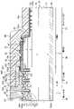
図1および図2に示されるように、SiC半導体装置は、トレンチゲート構造のMOSFET素子が形成されるセル部1と、このセル部1を囲む外周部2とを有する構成とされている。外周部2は、ガードリング部2aと、ガードリング2a部よりも内側に配置される繋ぎ部2bとを有する構成とされている。言い換えると、外周部2は、ガードリング部2aと、セル部1とガードリング部2aとの間に配置される繋ぎ部2bとを有する構成とされている。なお、本実施形態では、1つのセル部1とこのセル部1を囲む外周部2とを有する構成について説明するが、複数のセル部1を有するようにしてもよい。この場合は、各セル部1の間に位置する部分も外周部2となるため、例えば、SiC半導体装置の略中央部に外周部2が位置する場合もあり得る。 As shown in FIGS. 1 and 2, the SiC semiconductor device has a
SiC半導体装置は、図2に示されるように、半導体基板10を用いて構成されている。具体的には、半導体基板10は、SiCからなる高濃度不純物層を構成するn+型の基板11を有している。そして、基板11上には、基板11よりも低不純物濃度のSiCからなるn-型のドリフト層12がエピタキシャル成長させられている。ドリフト層12上には、p型のベース領域13がエピタキシャル成長させられ、さらにベース領域13の表層部にn+型のソース領域14が形成されている。なお、半導体基板10の一面100aは、ベース領域13側の面であるソース領域14の表面等で構成され、半導体基板10の他面100bは、基板11の裏面等で構成される。The SiC semiconductor device is constructed using a
基板11は、例えば、n型不純物濃度が1.0×10¹⁹/cm3とされ、表面が(0001)Si面とされている。ドリフト層12は、基板11よりも低不純物濃度で構成され、例えば、n型不純物濃度が0.5~2.0×1016/cm13とされている。The
ベース領域13は、チャネル領域が形成される部分であり、例えば、p型不純物濃度が2.0×10¹⁷/cm3程度とされ、厚さが300nmで構成されている。ソース領域14は、ドリフト層12よりも高不純物濃度とされ、例えば、表層部におけるn型不純物濃度が2.5×1018~1.0×1019/cm13、厚さが0.5μm程度で構成されている。なお、本実施形態では、ソース領域14が第1高不純物濃度領域に相当している。The
セル部1および繋ぎ部2bでは、基板11の表面側においてベース領域13が残されており、ガードリング部2aでは、ベース領域13を貫通してドリフト層12に達するように凹部10aが形成されている。このような構造とすることでメサ構造が構成されている。 In
また、セル部1および繋ぎ部2bでは、ベース領域13の表面にp型高濃度層によって構成されるコンタクト領域13aが形成されている。 Further, in the
さらに、セル部1では、ベース領域13よりも下方、つまりドリフト層12の表層部にp型のディープ層15が形成されている。ディープ層15は、ベース領域13よりもp型不純物濃度が高くされている。ディープ層15は、図2の紙面垂直方向、すなわち後述するトレンチゲート構造と同方向を長手方向として延設されている。具体的には、ディープ層15は、ドリフト層12に複数本が等間隔に配置され、互いに交点なく離れて配置されたストライプ状のトレンチ15a内に備えられている。各ディープ層15は、例えば、p型不純物濃度が1.0×10¹⁷~1.0×1019cm3、幅0.7μm、深さ2.0μm程度で構成されている。Furthermore, in the
また、半導体基板10には、一面100a側からベース領域13およびソース領域14を貫通してドリフト層12に達するように、例えば、幅が0.8μm、深さが1.0μmのゲートトレンチ16が形成されている。言い換えると、ベース領域13およびソース領域14は、ゲートトレンチ16の側面と接するように配置されている。ゲートトレンチ16は、本実施形態では、図2の紙面左右方向を幅方向、紙面垂直方向を長手方向、紙面上下方向を深さ方向とし、複数本が平行に等間隔に形成されている。つまり、本実施形態では、ゲートトレンチ16は、ドリフト層12とベース領域13との積層方向(以下では、単に積層方向ともいう)と交差する方向、詳しくは直交する方向に延設されている。言い換えると、本実施形態では、複数のゲートトレンチ16は、基板11の面方向における一方向に沿って延設されている。そして、ゲートトレンチ16は、延設方向の先端部で引き回されることで環状構造とされている。なお、ゲートトレンチ16は、複数本が平行に等間隔で形成されたストライプ状とされていてもよい。 Further, in the
そして、ゲートトレンチ16は、ゲート電極17およびゲート絶縁膜18によって埋め尽くされている。すなわち、ベース領域13のうちのゲートトレンチ16の側面に位置している部分を、縦型MOSFET素子の作動時にソース領域14とドリフト層12との間を繋ぐチャネル領域とすると、チャネル領域を含むゲートトレンチ16の内壁面にゲート絶縁膜18が形成されている。ゲート絶縁膜18は、例えば熱酸化膜等によって構成されている。そして、ゲート絶縁膜18の表面には、ドープドPoly-Siにて構成されたゲート電極17が形成されている。 The
なお、ゲート絶縁膜18は、ゲートトレンチ16の内壁面以外の表面にも形成されている。具体的には、ゲート絶縁膜18は、半導体基板10の一面100aの一部も覆うように形成されている。より詳しくは、ゲート絶縁膜18は、ソース領域14の表面の一部も覆うように形成されている。言い換えると、ゲート絶縁膜18には、ゲート電極17が配置される部分と異なる部分において、コンタクト領域13aおよびソース領域14の残部を露出させるコンタクトホール18aが形成されている。 The
また、ゲート絶縁膜18は、繋ぎ部2bにおけるベース領域13の表面にも形成されている。ゲート電極17についても、ゲート絶縁膜18と同様に、繋ぎ部2bにおけるゲート絶縁膜18の表面上まで延設されている。以上のようにして、本実施形態のトレンチゲート構造が構成されている。 The
そして、半導体基板10の一面100a上には、ゲート電極17やゲート絶縁膜18等を覆うように、層間絶縁膜19が形成されている。なお、層間絶縁膜19は、BPSG等で構成されており、ゲート絶縁膜18より柔らかい材料で構成されている。 An interlayer insulating
層間絶縁膜19には、コンタクトホール18aと連通してソース領域14およびコンタクト領域13aを露出させるコンタクトホール19aが形成されている。また、層間絶縁膜19には、ゲート電極17のうちの繋ぎ部2bまで延設された部分を露出させるコンタクトホール19bが形成されている。つまり、層間絶縁膜19には、セル部1にコンタクトホール19aが形成され、外周部2にコンタクトホール19bが形成されている。そして、コンタクトホール19a、19bは、開口する領域がセル部1の方が外周部2よりも多いため、セル部1の方が外周部2よりも密に形成されている。 A
なお、層間絶縁膜19に形成されたコンタクトホール19aは、ゲート絶縁膜18に形成されたコンタクトホール18aと連通するように形成されており、当該コンタクトホール18aと共に1つのコンタクトホールとして機能する。このため、以下では、コンタクトホール18aおよびコンタクトホール19aを纏めてコンタクトホール18bとも称する。また、コンタクトホール18bのパターンは、任意であり、例えば複数の正方形のものを配列させたパターン、長方形のライン状のものを配列させたパターン、または、ライン状のものを並べたパターン等が挙げられる。本実施形態では、コンタクトホール18bは、ゲートトレンチ16の長手方向に沿ったライン状とされている。 The
層間絶縁膜19上には、コンタクトホール18bを通じてソース領域14およびコンタクト領域13aと電気的に接続されるソース電極20が形成されている。また、層間絶縁膜19上には、コンタクトホール19bを通じてゲート電極17と電気的に接続されるゲート配線30が形成されている。なお、本実施形態では、ソース電極20が第1電極に相当している。 A
本実施形態では、ソース電極20は次のようにしてソース領域14およびコンタクト領域13aと接続されている。具体的には、ソース領域14およびコンタクト領域13aには、コンタクトホール18bから露出する部分に、Ni(ニッケル)等の金属を用いて構成された金属シリサイド21が形成されている。この金属シリサイド21は、ソース領域14およびコンタクト領域13aとソース電極20との間の接触抵抗の低減のために備えられている。 In this embodiment, the
そして、金属シリサイド21上には、Ti(チタン)やTiN(窒化チタン)等で構成されるバリアメタル22が形成されている。なお、バリアメタル22は、コンタクトホール18bの壁面や層間絶縁膜19の表面にも沿って形成されている。このバリアメタル22は、本実施形態では、後述するようにソース電極20がAl-Si層で構成されるため、Al-Si層に含まれるAlが半導体基板10側や層間絶縁膜19側に拡散することを抑制する役割を果たすものである。また、このバリアメタル22は、金属シリサイド21内のNiがAl-Si層側に拡散することを抑制する役割も果たす。 A
そして、ソース電極20は、バリアメタル22上に配置されることにより、バリアメタル22および金属シリサイド21を介してソース領域14およびコンタクト領域13aと接続されている。本実施形態では、ソース電極20は、Alを主成分とするAl-Si層で構成されている。なお、ソース電極20は、Al-Si層ではなく、Alのみで構成されたり、Alを主成分とする他の材料で構成されていてもよい。そして、ソース電極20は、本実施形態では、セル部1と外周部2との境界部分近傍まで形成されている。
ゲート配線30は、次のようにしてゲート電極17と接続されている。すなわち、ゲート電極17には、コンタクトホール19bから露出する部分に、TiN等で構成されるバリアメタル31が形成されている。なお、バリアメタル31は、コンタクトホール19bの壁面や層間絶縁膜19の表面にも沿って形成されている。このバリアメタル31は、本実施形態では、後述するように、ゲート配線30がAl-Siで構成されるため、Al-Siに含まれるAlが半導体基板10側や層間絶縁膜19側に拡散することを抑制する役割を果たすものである。 The
そして、ゲート配線30は、バリアメタル31上に配置されることにより、バリアメタル31を介してゲート電極17と接続されている。本実施形態では、ゲート配線30は、ソース電極20と同様に、Al-Si層で構成されている。そして、このゲート配線30は、適宜引き回され、図1に示すパッド3のうちの1つと電気的に接続されている。 The
なお、本実施形態では、詳細な説明はしないが、SiC半導体装置は、電流センスや温度センス等が適宜形成されている。そして、これらの各センスは、図1に示す各パッド3と適宜電気的に接続される。 Although detailed description is not given in this embodiment, the SiC semiconductor device is appropriately formed with a current sensor, a temperature sensor, and the like. Each of these senses is appropriately electrically connected to each
また、ソース電極20上には、ソース電極20を通じて外部との接続を図る際のはんだ濡れ性を向上させるためのNiメッキ層23およびAu層24が積層されて形成されている。なお、ソース電極20はセル部1と外周部2との境界部分まで形成されているが、Niメッキ層23およびAu層24は、当該境界部分まで形成されていない。つまり、Niメッキ層23およびAu層24は、ソース電極20の外縁部を露出させるように形成されている。なお、特に図示していないが、ゲート配線30上にも、Niメッキ層を介してAu層が形成されていてもよい。 A
基板11の裏面(すなわち、半導体基板10の他面100b)側には、基板11と電気的に接続され、第2電極に相当するドレイン電極40が形成されている。このような構造により、nチャネルタイプの反転型のトレンチゲート構造のMOSFETが構成されている。そして、このようなMOSFETが複数セル配置されることでセル部1が構成されている。なお、本実施形態では、基板11がドレイン層を構成し、第2高不純物濃度領域に相当している。 A
ガードリング部2aでは、上記のように、ソース領域14およびベース領域13を貫通してドリフト層12に達するように凹部10aが形成されている。このため、セル部1から離れた位置ではソース領域14およびベース領域13が除去されて、ドリフト層12が露出させられている。そして、基板11の厚み方向において、凹部10aよりも内側に位置するセル部1や繋ぎ部2bが島状に突き出したメサ部となっており、セル部1および繋ぎ部2bとガードリング部2aとの間において段差が構成されている。 In
また、凹部10aの下方に位置するドリフト層12の表層部には、セル部1を囲むように、複数本のp型のガードリング50が備えられている。本実施形態では、ガードリング50の上面レイアウトは、積層方向から視たき、四隅が丸められた四角形状や円形状等とされている。ガードリング50は、例えば、ドリフト層12の表層部に形成されたトレンチ50a内に配置され、エピタキシャル成長によるp型のエピタキシャル膜によって構成されている。 In addition, a plurality of p-type guard rings 50 are provided so as to surround the
なお、積層方向から視るとは、言い換えると、基板11の面方向に対する法線方向から視ることである。また、図示していないが、必要に応じてガードリング50よりも外周にEQR(Equi Potential Ringの略)構造が備えられることにより、セル部1を囲む外周耐圧構造が備えられたガードリング部2aが構成されている。 In other words, viewing from the stacking direction means viewing from the direction normal to the surface direction of the
また、セル部1からガードリング部2aに至るまでの間を繋ぎ部2bとし、繋ぎ部2bおよびガードリング部2aの内周側には、ドリフト層12の表層部にp型のリサーフ層51が形成されている。例えば、積層方向から視たとき、セル部1を囲むように繋ぎ部2bが形成されており、さらに繋ぎ部2bの外側を囲むように、四隅が丸められた四角形状のガードリング50が複数本形成されている。そして、リサーフ層51は、セル部1の周りを囲みつつ、ガードリング部2aに至るように延設されている。このリサーフ層51も、ドリフト層12の表層部に形成したトレンチ51a内に配置され、エピタキシャル成長によるエピタキシャル膜によって構成されている。 A connecting
このようなリサーフ層51を形成することにより、等電位線をガードリング部2a側に導くことができ、繋ぎ部2b内で電界集中する部位が発生しないようすることができる。このため、耐圧低下を抑制することが可能となる。 By forming such a
さらに、繋ぎ部2bおよびガードリング部2aを覆うように、ポリイミド等によって構成される保護膜60が形成されている。本実施形態では、保護膜60は、ソース電極20とドレイン電極40との間で沿面放電が発生することを抑制するため、外周部2からセル部1の外縁部上まで形成されている。具体的には、保護膜60は、ソース電極20のうちのNiメッキ層23およびAu層24から露出する部分を覆い、かつNiメッキ層23およびAu層24を露出させるように形成されている。つまり、保護膜60は、ソース電極20における外周部2側の外縁部を覆うように形成されている。本実施形態では、このように保護膜60が形成されており、保護膜60の下方にもトレンチゲート構造が位置する構成とされている。 Furthermore, a
以下では、積層方向において、セル部1のうちの保護膜60と重なる部分を第1セル部1aとし、セル部1のうちの保護膜60と重ならない部分を第2セル部1bとして説明する。つまり、以下では、セル部1のうちの保護膜60の下方に位置する部分を第1セル部1aとし、セル部1のうちの保護膜60の下方と異なる部分に位置する部分を第2セル部1bとして説明する。このため、ソース電極20は、第1セル部1aでは保護膜60で覆われており、第2セル部1bでは保護膜60から露出した状態となっている。なお、図1に示されるように、セル部1を囲むように外周部2が配置されているため、第1セル部1aは、第2セル部1bを囲むように位置している。 Hereinafter, a portion of the
以上が本実施形態のSiC半導体装置における基本的な構成である。なお、本実施形態では、N+型、N-型が第1導電型に相当しており、P型、P+型が第2導電型に相当している。The above is the basic configuration of the SiC semiconductor device of the present embodiment. In this embodiment, the N+ type and N− type correspond to the first conductivity type, and the P type and P+ type correspond to the second conductivity type.
そして、ソース電極20において、半導体基板10の一面100aと、ソース電極20における半導体基板10の一面100aと反対側の表面との間の長さを膜厚する。この場合、本実施形態では、ソース電極20は、第1セル部1aに位置する第1部位20aは、第2セル部1bに位置する第2部位20bよりも膜厚が厚くなる部分を有する構成とされている。本実施形態では、ソース電極20は、第1部位20aが第2部位20bより膜厚が全体的に厚くされており、第1部位20aと第2部位20bとの境界部に段差20cを有する形状とされている。 Then, in the
なお、このようなソース電極20は、例えば、次のように形成される。すなわち、金属シリサイド21およびバリアメタル22を形成した後、ソース電極20を構成するAl-Si膜をスパッタ等で形成する。その後、第2部位20bとなる部分に対して第1部位20aとなる部分よりも多い回数のエッチングを行うことにより、第2部位20bの膜厚を第1部位20aの膜厚より薄くする。これにより、第1部位20aが第2部位20bの膜厚より厚くされたソース電極20が形成される。 In addition, such a
以上が本実施形態における半導体装置の構成である。このようなSiC半導体装置は、MOSFET素子をオンするときには、ゲート電極17に対してトレンチゲート構造における閾値電圧Vt以上の電圧を印加することにより、ゲートトレンチ16の側面に位置するベース領域13の表面部にチャネル領域を形成する。これにより、ソース電極20からソース領域14に電子が注入されて、当該電子がソース領域14からチャネル領域、ドリフト層12を介してドレイン電極40に流れる。このようにして、ソース電極20とドレイン電極40との間に電流が流れてオン状態となる。 The above is the configuration of the semiconductor device according to the present embodiment. In such a SiC semiconductor device, when the MOSFET element is turned on, a voltage equal to or higher than the threshold voltage Vt in the trench gate structure is applied to the
この際、ソース電極20内では、Niメッキ層23との接触箇所と、ソース領域14との接触箇所との間に電流が流れる。そして、ソース電極20は、電流が流れることによって発熱し、発熱は、抵抗が大きくなるほど大きくなる。 At this time, in the
この場合、ソース電極20内では、第1部位20aでは、ソース領域14との接触箇所からNiメッキ層23との接触箇所に向かい、基板11の面方向に沿っても電流が流れる。このため、本実施形態では、第1部位20aは、第2部位20bよりも膜厚が厚くなる部分を有する構成とされている。したがって、第1部位20aでは、膜厚が第2部位20bと同じ厚さとされている場合と比較すると、電流の流れ方向に対する断面積が大きくなるため、抵抗が小さくなる。したがって、第1部位20aでの発熱を低減することができる。 In this case, in the
なお、ソース電極20内では、第2部位20bでは、ソース領域14との接触箇所からNiメッキ層23との接触箇所に向かい、積層方向に沿って電流が流れる。 In the
また、逆バイアス時には、繋ぎ部2bでは、リサーフ層51が形成されていることで等電位線のせり上がりが抑制されて、ガードリング部2a側に向かうようにされる。そして、ガードリング部2aでは、ガードリング50によって等電位線の間隔が外周方向に向かって広がりながら終端させられるようになり、ガードリング部2aでも所望の耐圧を得ることができる。したがって、所望の耐圧を得ることが可能なSiC半導体装置とすることができる。 In the reverse bias, the
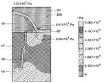
ここで、第1部位20aおよび第2部位20bが同じ膜厚とされているSiC半導体装置がオン状態である場合の温度分布および応力分布について、図3、図4Aおよび図4Bを参照しつつ説明する。なお、以下では、第1部位20aおよび第2部位20bが同じ膜厚とされているSiC半導体装置を単に従来のSiC半導体装置とも称する。また、図3は、ソース電極20上にNiメッキ層23およびAu層24を介してはんだ70を配置した場合のシミュレーション結果であり、ソース領域14等の詳細な構成要素は省略して示してある。また、図4Aおよび図4B中の数値は、ミーゼス応力を示している。 Here, the temperature distribution and stress distribution when the SiC semiconductor device in which the
まず、図3に示されるように、従来のSiC半導体装置をオン状態にすると、保護膜60の熱伝導率がソース電極20より低く放熱性が低いため、第1セル部1aの方が第2セル部1bよりも温度が高くなっていることが確認される。そして、図4Aおよび図4Bに示されるように、第1部位20aでは、第2部位20bより発生する熱応力が大きく、ゲート絶縁膜18に印加される熱応力が大きくなっていることが確認される。つまり、第1部位20a近傍のゲート絶縁膜18には、第2部位20b近傍のゲート絶縁膜18より大きな熱応力が印加されていることが確認される。 First, when the conventional SiC semiconductor device is turned on, as shown in FIG. It is confirmed that the temperature is higher than that of the
このため、本実施形態では、上記のように、ソース電極20は、第1部位20aの膜厚が第2部位20bの膜厚よりも厚くなるようにしている。したがって、本実施形態の半導体装置では、SiC半導体装置がオン状態である際、第1部位20aの膜厚が第2部位20bの膜厚と同じとされている場合と比較して、第1部位20aでの発熱を低減できる。したがって、第1部位20a近傍のゲート絶縁膜18に大きな熱応力が印加されることを抑制できる。 For this reason, in the present embodiment, as described above, the
以上説明したように、本実施形態では、ソース電極20は、第1部位20aが第2部位20bよりも膜厚が厚くなる部分を有する構成とされている。このため、SiC半導体装置がオン状態である際、第1部位20aが第2部位20bの膜厚と同じ厚さとされている場合と比較すると、第1部位20aでの発熱を低減できる。したがって、第1部位20aからゲート絶縁膜18に大きな応力が印加されることを抑制でき、ゲート絶縁膜18が破壊されることを抑制できる。 As described above, in the present embodiment, the
また、本実施形態では、ソース電極20は、第2部位20bが第1部位20aよりも膜厚が薄くされている。このため、第2部位20bの膜厚が第1部位20aの膜厚と等しくされている場合と比較して、第2部位20bでは、電流の流れ方向に沿った長さを短くできるため、抵抗を小さくできる。したがって、電流損失の低減を図ることができる。 In addition, in the present embodiment, the
さらに、本実施形態では、第1部位20aと第2部位20bとは、段差20cによって膜厚が変化させられており、段差20cは、エッチングの回数を変更する等によって容易に形成される。つまり、本実施形態では、エッチングにより、第1部位20aと第2部位20bとの厚さを容易に変更できるため、製造工程が複雑化することも抑制できる。 Furthermore, in the present embodiment, the thickness of the
(第2実施形態)
第2実施形態について説明する。本実施形態は、第1実施形態に対し、ソース電極20の形状を変更したものである。その他に関しては、第1実施形態と同様であるため、ここでは説明を省略する。(Second embodiment)
A second embodiment will be described. In this embodiment, the shape of the
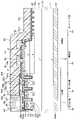
本実施形態では、図5に示されるように、バリアメタル22上には、Ti/Cu(銅)の積層膜で構成されるシード層25が形成されている。そして、ソース電極20は、シード層25上に形成されている。なお、本実施形態では、ソース電極20は、Cu等のメッキ膜で構成されている。 In this embodiment, as shown in FIG. 5, a
また、ソース電極20は、第2部位20bにおける第1部位20a側の外縁部から内縁部に向かって膜厚が徐々に薄くなる構成とされている。つまり、ソース電極20は、上記第1実施形態と同様に、第1部位20aが第2部位20bより膜厚が厚くなる部分を有する構成とされている。なお、本実施形態では、ソース電極20は、第1部位20aと第2部位20bとの境界に段差20cが形成されていない構成とされている。 In addition, the
このようなソース電極20は、次のように形成される。すなわち、まず、バリアメタル22上にシード層25を形成する。なお、このシード層25は、メッキ膜を形成し易くするためのものである。そして、シード層25上に、電界メッキ法によってCuのメッキ膜を構成することにより、ソース電極20が形成される。 Such a
この際、上記のように、第1セル部1aは、第2セル部1bよりも外周部2側の部分である。そして、層間絶縁膜19に形成されるコンタクトホール19a、19bは、外周部2よりもセル部1の方が密に形成される。このため、電界メッキ法によってメッキ膜を形成した場合、メッキ膜は、外周部2側では、コンタクトホール19bに入り込む部分が少なくなり、厚く形成され易い。そして、第1セル部1aが第2セル部1bよりも外周部2側に位置するため、メッキ膜は、第1セル部1aに形成される部分が第2セル部1bに形成される部分よりも外周部2の影響を受け易い。つまり、メッキ膜は、第1セル部1aに形成される部分が第2セル部1bに形成される部分よりも外周部2の影響を受けて厚くなり易い。このため、ソース電極20は、第1部位20aが第2部位20bよりも膜厚が厚くなり易く、また、第1部位20aと第2部位20bとの間に段差20cが形成されない構成となる。 At this time, as described above, the
なお、本実施形態では、バリアメタル31上にもシード層25が形成されており、ゲート配線30もメッキ膜によって構成される。 In this embodiment, the
以上説明したように、ソース電極20は、第2部位20bが第1部位20a側の外縁部から内縁部に向かって膜厚が徐々に薄くなる構成とされていても、上記第1実施形態と同様の効果を得ることができる。また、この構成では、複数回のエッチングを行う必要がなく、製造工程の簡略化を図ることもできる。 As described above, even if the
(第3実施形態)
第3実施形態について説明する。本実施形態は、第1実施形態に対し、ソース電極20の形状を変更したものである。その他に関しては、第1実施形態と同様であるため、ここでは説明を省略する。(Third Embodiment)
A third embodiment will be described. In this embodiment, the shape of the
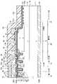
本実施形態では、図6に示されるように、ソース電極20の第1部位20aは、第1金属部201と、第1金属部201よりも抵抗率が小さい材料で構成された第2金属部202とを有する構成とされている。そして、第2金属部202は、第1金属部201内に配置された構成とされている。つまり、第1部位20aは、第1金属部201、第2金属部202、第1金属部201が順に積層された部分を有する構成とされている。なお、本実施形態では、第1金属部201は、Al-Si層で構成され、第2金属部202は、TiN/Tiの積層膜で構成されている。 In this embodiment, as shown in FIG. 6, the
このようなソース電極20は、次のように形成される。すなわち、まず、第1金属部201を構成するAl-Si膜をスパッタ等によって形成する。なお、このAl-Si膜は、第2部位20bの膜厚より僅かに厚く形成される。そして、このAl-Si膜上に、スパッタ等により、第2金属部202を構成する金属膜を形成する。次に、当該金属膜のうちの第2セル部1bに位置する部分をエッチング等によって除去する。この際、第2セル部1bでは、Al-Si膜がオーバーエッチングされる。このため、Al-Si膜は、第2セル部1bに位置する部分が第1セル部1aに位置する部分よりも薄くなる。その後、金属膜を覆うように、再びAl-Si膜を形成する。これにより、第2金属部202が第1金属部201内に配置されたソース電極20が形成される。 Such a
以上説明したように、本実施形態では、ソース電極20の第1部位20aは、第1金属部201、第1金属部201より抵抗率の小さい材料で構成された第2金属部202を有する構成とされている。このため、第1部位20aが第1金属部201のみで構成されている場合と比較して、さらに抵抗を小さくできる。したがって、SiC半導体装置がオン状態である際、さらに第1部位20aの発熱を低減できる。 As described above, in the present embodiment, the
また、第2金属部202上に第1金属部201を配置することにより、第1部位20aを第1金属部201のみで構成する場合と比較して、第2金属部202上に位置する第1金属部201は、粒径が小さくなり易く、粒子が緻密に形成され易い。また、SiC半導体装置は、オン状態である際、ソース電極20、Niメッキ層23、保護膜60との三重点において、各部材の熱膨張係数が異なるために大きな応力が発生し易い。このため、本実施形態では、第1部位20aを第1金属部201のみで構成する場合と比較して、ソース電極20が破壊されることを抑制することもできる。 In addition, by arranging the
(第3実施形態の変形例)
第3実施形態の変形例について説明する。第3実施形態において、図7に示されるように、第1部位20aは、第1金属部201上に第2金属部202が積層されることで構成されていてもよい。このような構成としても、上記第3実施形態と同様の効果を得ることができる。(Modified example of the third embodiment)
A modification of the third embodiment will be described. In the third embodiment, as shown in FIG. 7, the
(第4実施形態)
第4実施形態について説明する。本実施形態は、第1実施形態に対し、ソース電極20の形状を変更したものである。その他に関しては、第1実施形態と同様であるため、ここでは説明を省略する。(Fourth embodiment)
A fourth embodiment will be described. In this embodiment, the shape of the
本実施形態では、図8に示されるように、ソース電極20は、第1部位20aと第2部位20bとの膜厚が等しくされている。しかしながら、ソース電極20は、第1部位20aが第2部位20bより抵抗率が小さい材料で構成されている。本実施形態では、ソース電極20は、第1部位20aがCu層で構成され、第2部位20bがAl-Si層で構成される。 In this embodiment, as shown in FIG. 8, the thickness of the
また、本実施形態では、第1部位20aがCu層で構成されると共に第2部位20bがAl-Si層で構成されるため、第2部位20bの方が第1部位20aよりも柔らかい材料で構成される。つまり、第2部位20bは、第1部位20aよりも硬度が小さい材料で構成される。 In addition, in the present embodiment, the
以上説明したように、本実施形態では、ソース電極20は、第1部位20aが第2部位20bより抵抗率が小さい材料で構成されている。このため、SiC半導体装置がオン状態である際、第1部位20aが第2部位20bと同じ材料で構成されている場合と比較すると、第1部位20aでの発熱を低減でき、上記第1実施形態と同様の効果を得ることができる。 As described above, in the present embodiment, the
また、本実施形態では、ソース電極20は、第2部位20bが第1部位20aより硬度が小さい材料で構成されている。このため、SiC半導体装置がオン状態である際、第2部位20bが第1部位20aと同じ材料で構成されている場合と比較して、第2部位20bにて応力を緩和し易くできる。このため、半導体装置が破壊されることを抑制できる。 In addition, in the present embodiment, the
(他の実施形態)
本発明は上記した実施形態に限定されるものではなく、特許請求の範囲に記載した範囲内において適宜変更が可能である。(Other embodiments)
The present invention is not limited to the above-described embodiments, and can be appropriately modified within the scope of the claims.
例えば、上記各実施形態では、SiC半導体装置を例に挙げて説明した。しかしながら、SiC半導体装置は1例であり、その他の半導体材料、すなわちシリコンや化合物半導体を用いた半導体装置に上記各実施形態を適用することもできる。 For example, in each of the above-described embodiments, the SiC semiconductor device has been described as an example. However, the SiC semiconductor device is only an example, and the above embodiments can also be applied to semiconductor devices using other semiconductor materials, ie, silicon and compound semiconductors.
また、上記各実施形態では、第1導電型をn型、第2導電型をp型としたnチャネルタイプのMOSFET素子を例に挙げて説明したが、各構成要素の導電型を反転させたpチャネルタイプのMOSFET素子としてもよい。また、上記各実施形態は、半導体素子としてのMOSFET素子に加えて、同様の構造のIGBT素子に対しても適用することができる。IGBT素子は、上記各実施形態に対して基板11の導電型をn型からp型に変更するだけであり、その他の構造は上記各実施形態と同様である。さらに、縦型のMOSFET素子としてトレンチゲート構造のものを例に挙げて説明したが、トレンチゲート構造のものに限らず、プレーナ型のものであってもよい。 Further, in each of the above-described embodiments, an n-channel type MOSFET element in which the first conductivity type is n-type and the second conductivity type is p-type has been described as an example. A p-channel type MOSFET element may be used. Moreover, each of the above embodiments can be applied to an IGBT element having a similar structure in addition to a MOSFET element as a semiconductor element. The IGBT element is the same as the above embodiments except that the conductivity type of the
さらに、上記各実施形態では、ソース領域14がイオン注入によって形成される場合を想定しているが、ソース領域14をエピタキシャル成長によって形成することもできる。 Furthermore, in each of the above embodiments, the
また、上記第1実施形態では、第1部位20aと第2部位20bとの境界部に段差20cを有する形状とされていなくてもよい。例えば、図9に示されるように、段差20cは、第2部位20b内に位置する構成とされていてもよい。つまり、ソース電極20は、第2部位20bにおける第1部位20a側の外縁部が第1部位20aと同じ構成とされ、膜厚が厚くなる構成とされていてもよい。さらに、特に図示しないが、段差20cは、第1部位20a内に位置する構成とされていてもよい。つまり、ソース電極20は、第1部位20aにおける第2部位20b側の内縁部が第2部位20bと同じ構成とされていてもよい。このような構成としても、第1部位20aは、第2部位20bより膜厚が厚い部分を有するため、上記第1実施形態と同様の効果を得ることができる。 Further, in the above-described first embodiment, the boundary portion between the
また、図10に示されるように、保護膜60は、Niメッキ層23およびAu層24側の部分がテーパ形状とされていてもよい。 Moreover, as shown in FIG. 10, the
そして、特に図示しないが、上記第2実施形態では、ソース電極20は、第1部位20aにおける内縁部から第2部位20bにおける内縁部に向かって膜厚が徐々に薄くなる構成とされていてもよい。また、特に図示しないが、上記第3実施形態では、第2部位20bにおける第1部位20a側の外縁部が第1部位20aと同様の構成とされていてもよい。同様に、上記第3実施形態では、第1部位20aにおける第2部位20b側の内縁部が第2部位20bと同様の構成とされていてもよい。さらに、特に図示しないが、上記第4実施形態では、第2部位20bにおける第1部位20a側の外縁部が第1部位20aと同様の構成とされていてもよい。同様に、上記第4実施形態では、第1部位20aにおける第2部位20b側の内縁部が第2部位20bと同様の構成とされていてもよい。さらに、これらの構成においても、保護膜60は、Niメッキ層23およびAu層24側の部分がテーパ形状とされていてもよい。 Although not shown, in the second embodiment, the thickness of the
そして、上記各実施形態を適宜組み合わせることができる。例えば、第1~第3実施形態に上記第4実施形態を組み合わせ、第1部位20aが第2部位20bより抵抗率の小さい材料で構成されるようにしてもよい。さらに、上記各実施形態を組み合わせたもの同士を適宜組み合わせてもよい。 Further, each of the above embodiments can be appropriately combined. For example, the fourth embodiment may be combined with the first to third embodiments so that the
1 セル部
1a 第1セル部
1b 第2セル部
2 外周部
10 半導体基板
11 基板(第2高不純物濃度領域)
12 ドリフト層
13 ベース領域
14 ソース領域(第1高不純物濃度領域)
17 ゲート電極
18 ゲート絶縁膜
18a コンタクトホール
20 ソース電極(第1電極)
40 ドレイン電極(第2電極)
60 保護膜
100a 一面
12
17
40 drain electrode (second electrode)
60
Claims (12)
Translated fromJapanese前記セル部は、
第1導電型のドリフト層(12)と、
前記ドリフト層上に形成された第2導電型のベース領域(13)と、
前記ベース領域の表層部に形成され、前記ドリフト層よりも高不純物濃度とされた第1導電型の第1高不純物濃度領域(14)と、
前記ドリフト層を挟んで前記ベース領域と反対側に形成され、前記ドリフト層よりも高不純物濃度とされた第1導電型または第2導電型の第2高不純物濃度領域(11)と、を有し、前記ベース領域側の面を一面(100)とする半導体基板(10)と、
前記第1高不純物濃度領域と前記ドリフト層との間に挟まれた前記ベース領域の表面を含んで形成されたゲート絶縁膜(18)と、前記ゲート絶縁膜上に配置されたゲート電極(17)と、を有する前記ゲート構造と、
前記ゲート絶縁膜のうちの前記ゲート電極が配置される部分と異なる部分に形成されたコンタクトホール(18a)を通じて前記ベース領域および前記第1高不純物濃度領域と電気的に接続される第1電極(20)と、
前記第2高不純物濃度領域と電気的に接続される第2電極(40)と、を備え、
前記セル部および前記外周部は、前記外周部から前記セル部における前記外周部側の外縁部に渡り、前記第1電極における前記外周部側の部分を覆うように配置され、前記第1電極より熱伝導率が低い材料で構成された保護膜(60)を備え、
前記セル部のうちの、前記ドリフト層と前記ベース領域との積層方向において前記保護膜と重なる領域を第1セル部(1a)とし、前記第1セル部と異なる領域を第2セル部(1b)とすると、前記ゲート構造が前記第1セル部および前記第2セル部に形成されており、
前記第1電極は、前記第1セル部に位置する部位を第1部位(20a)とし、前記第2セル部に位置する部位を第2部位(20b)とし、前記半導体基板の一面から前記第1電極のうちの前記一面と反対側の表面までの間の長さを膜厚とすると、前記第1部位が前記第2部位より膜厚が厚い部分を有し、
前記第2部位は、前記第1部位側の外縁部から内縁部に向かって膜厚が薄くなる構成とされている半導体装置。A semiconductor device having a cell portion (1) and an outer peripheral portion (2) surrounding the cell portion, wherein a plurality of gate structures are formed in the cell portion,
The cell part is
a first conductivity type drift layer (12);
a second conductivity type base region (13) formed on the drift layer;
A first high impurity concentration region (14) of a first conductivity type formed in a surface layer portion of the base region and having an impurity concentration higher than that of the drift layer;
a second high impurity concentration region (11) of a first conductivity type or a second conductivity type formed on the opposite side of the base region with the drift layer interposed therebetween and having an impurity concentration higher than that of the drift layer; a semiconductor substrate (10) having a surface (100) facing the base region;
a gate insulating film (18) formed including the surface of the base region sandwiched between the first high impurity concentration region and the drift layer; and a gate electrode (17) disposed on the gate insulating film. ), and the gate structure having
a first electrode electrically connected to the base region and the first high impurity concentration region through a contact hole (18a) formed in a portion of the gate insulating film different from the portion where the gate electrode is arranged; 20) and
a second electrode (40) electrically connected to the second high impurity concentration region;
The cell portion and the outer peripheral portion extend from the outer peripheral portion to the outer edge portion of the cell portion on the outer peripheral side, and are arranged so as to cover a portion of the first electrode on the outer peripheral side. A protective film (60) made of a material with low thermal conductivity is provided,
In the cell portion, a region overlapping the protective film in the lamination direction of the drift layer and the base region is defined as a first cell portion (1a), and a region different from the first cell portion is defined as a second cell portion (1b). ), the gate structure is formed in the first cell portion and the second cell portion,
The first electrode has a portion located in the first cell portion as a first portion (20a), a portion located in the second cell portion as a second portion (20b), and a portion positioned in the second cell portion as a second portion (20b). When the film thickness is the length between the one surface of one electrode and the surface on the opposite side, the first portion has a portion thicker than the second portion,
In the semiconductor device, the film thickness of the second portion decreases from the outer edge toward the inner edge of the first portion .
前記第2部位は、前記第1金属部と同じ材料を用いて構成されている請求項1または2に記載の半導体装置。The first part has a first metal part (201) and a second metal part (202) having a lower resistivity than the first metal part,
3. The semiconductor device according to claim 1, wherein said second portion is made of the same material as said first metal portion.
前記セル部は、
第1導電型のドリフト層(12)と、
前記ドリフト層上に形成された第2導電型のベース領域(13)と、
前記ベース領域の表層部に形成され、前記ドリフト層よりも高不純物濃度とされた第1導電型の第1高不純物濃度領域(14)と、
前記ドリフト層を挟んで前記ベース領域と反対側に形成され、前記ドリフト層よりも高不純物濃度とされた第1導電型または第2導電型の第2高不純物濃度領域(11)と、を有し、前記ベース領域側の面を一面(100)とする半導体基板(10)と、
前記第1高不純物濃度領域と前記ドリフト層との間に挟まれた前記ベース領域の表面を含んで形成されたゲート絶縁膜(18)と、前記ゲート絶縁膜上に配置されたゲート電極(17)と、を有する前記ゲート構造と、
前記ゲート絶縁膜のうちの前記ゲート電極が配置される部分と異なる部分に形成されたコンタクトホール(18a)を通じて前記ベース領域および前記第1高不純物濃度領域と電気的に接続される第1電極(20)と、
前記第2高不純物濃度領域と電気的に接続される第2電極(40)と、を備え、
前記セル部および前記外周部は、前記外周部から前記セル部における前記外周部側の外縁部に渡り、前記第1電極における前記外周部側の部分を覆うように配置され、前記第1電極より熱伝導率が低い材料で構成された保護膜(60)を備え、
前記セル部のうちの、前記ドリフト層と前記ベース領域との積層方向において前記保護膜と重なる領域を第1セル部(1a)とし、前記第1セル部と異なる領域を第2セル部(1b)とすると、前記ゲート構造が前記第1セル部および前記第2セル部に形成されており、
前記第1電極は、前記第1セル部に位置する部位を第1部位(20a)とし、前記第2セル部に位置する部位を第2部位(20b)とし、前記半導体基板の一面から前記第1電極のうちの前記一面と反対側の表面までの間の長さを膜厚とすると、前記第1部位が前記第2部位より膜厚が厚い部分を有し、
前記第1部位は、第1金属部(201)と、前記第1金属部より抵抗率が小さくされた第2金属部(202)とを有しており、
前記第2部位は、前記第1金属部と同じ材料を用いて構成されている半導体装置。A semiconductor device having a cell portion (1) and an outer peripheral portion (2) surrounding the cell portion, wherein a plurality of gate structures are formed in the cell portion,
The cell part is
a first conductivity type drift layer (12);
a second conductivity type base region (13) formed on the drift layer;
A first high impurity concentration region (14) of a first conductivity type formed in a surface layer portion of the base region and having an impurity concentration higher than that of the drift layer;
a second high impurity concentration region (11) of a first conductivity type or a second conductivity type formed on the opposite side of the base region with the drift layer interposed therebetween and having an impurity concentration higher than that of the drift layer; a semiconductor substrate (10) having a surface (100) facing the base region;
a gate insulating film (18) formed including the surface of the base region sandwiched between the first high impurity concentration region and the drift layer; and a gate electrode (17) disposed on the gate insulating film. ), and the gate structure having
a first electrode electrically connected to the base region and the first high impurity concentration region through a contact hole (18a) formed in a portion of the gate insulating film different from the portion where the gate electrode is arranged; 20) and
a second electrode (40) electrically connected to the second high impurity concentration region;
The cell portion and the outer peripheral portion extend from the outer peripheral portion to the outer edge portion of the cell portion on the outer peripheral side, and are arranged so as to cover a portion of the first electrode on the outer peripheral side. A protective film (60) made of a material with low thermal conductivity is provided,
In the cell portion, a region overlapping the protective film in the lamination direction of the drift layer and the base region is defined as a first cell portion (1a), and a region different from the first cell portion is defined as a second cell portion (1b). ), the gate structure is formed in the first cell portion and the second cell portion,
The first electrode has a portion located in the first cell portion as a first portion (20a), a portion located in the second cell portion as a second portion (20b), and a portion positioned in the second cell portion as a second portion (20b). When the film thickness is the length between the one surface of one electrode and the surface on the opposite side, the first portion has a portion thicker than the second portion,
The first part has a first metal part (201) and a second metal part (202) having a lower resistivity than the first metal part,
The semiconductor device, wherein the second portion is made of the same material as the first metal portion .
前記第2金属部は、Tiを含んで構成されている請求項5に記載の半導体装置。The first metal part is configured to contain Al—Si,
6. The semiconductor device according to claim5 , wherein said second metal portion contains Ti.
前記セル部は、
第1導電型のドリフト層(12)と、
前記ドリフト層上に形成された第2導電型のベース領域(13)と、
前記ベース領域の表層部に形成され、前記ドリフト層よりも高不純物濃度とされた第1導電型の第1高不純物濃度領域(14)と、
前記ドリフト層を挟んで前記ベース領域と反対側に形成され、前記ドリフト層よりも高不純物濃度とされた第1導電型または第2導電型の第2高不純物濃度領域(11)と、を有し、前記ベース領域側の面を一面(100)とする半導体基板(10)と、
前記第1高不純物濃度領域と前記ドリフト層との間に挟まれた前記ベース領域の表面を含んで形成されたゲート絶縁膜(18)と、前記ゲート絶縁膜上に配置されたゲート電極(17)と、を有する前記ゲート構造と、
前記ゲート絶縁膜のうちの前記ゲート電極が配置される部分と異なる部分に形成されたコンタクトホール(18a)を通じて前記ベース領域および前記第1高不純物濃度領域と電気的に接続される第1電極(20)と、
前記第2高不純物濃度領域と電気的に接続される第2電極(40)と、を備え、
前記セル部および前記外周部は、前記外周部から前記セル部における前記外周部側の外縁部に渡り、前記第1電極における前記外周部側の部分を覆うように配置され、前記第1電極より熱伝導率が低い材料で構成された保護膜(60)を備え、
前記セル部のうちの、前記ドリフト層と前記ベース領域との積層方向において前記保護膜と重なる領域を第1セル部(1a)とし、前記第1セル部と異なる領域を第2セル部(1b)とすると、前記ゲート構造が前記第1セル部および前記第2セル部に形成されており、
前記第1電極は、前記第1セル部に位置する部位を第1部位(20a)とし、前記第2セル部に位置する部位を第2部位(20b)とし、前記半導体基板の一面から前記第1電極のうちの前記一面と反対側の表面までの間の長さを膜厚とすると、前記第1部位が前記第2部位より膜厚が厚い部分を有し、
前記第1電極は、前記第1部位が前記第2部位より抵抗率が小さい材料で構成されている半導体装置。A semiconductor device having a cell portion (1) and an outer peripheral portion (2) surrounding the cell portion, wherein a plurality of gate structures are formed in the cell portion,
The cell part is
a first conductivity type drift layer (12);
a second conductivity type base region (13) formed on the drift layer;
A first high impurity concentration region (14) of a first conductivity type formed in a surface layer portion of the base region and having an impurity concentration higher than that of the drift layer;
a second high impurity concentration region (11) of a first conductivity type or a second conductivity type formed on the opposite side of the base region with the drift layer interposed therebetween and having an impurity concentration higher than that of the drift layer; a semiconductor substrate (10) having a surface (100) facing the base region;
a gate insulating film (18) formed including the surface of the base region sandwiched between the first high impurity concentration region and the drift layer; and a gate electrode (17) disposed on the gate insulating film. ), and the gate structure having
a first electrode electrically connected to the base region and the first high impurity concentration region through a contact hole (18a) formed in a portion of the gate insulating film different from the portion where the gate electrode is arranged; 20) and
a second electrode (40) electrically connected to the second high impurity concentration region;
The cell portion and the outer peripheral portion extend from the outer peripheral portion to the outer edge portion of the cell portion on the outer peripheral side, and are arranged so as to cover a portion of the first electrode on the outer peripheral side. A protective film (60) made of a material with low thermal conductivity is provided,
In the cell portion, a region overlapping the protective film in the lamination direction of the drift layer and the base region is defined as a first cell portion (1a), and a region different from the first cell portion is defined as a second cell portion (1b). ), the gate structure is formed in the first cell portion and the second cell portion,
The first electrode has a portion located in the first cell portion as a first portion (20a), a portion located in the second cell portion as a second portion (20b), and a portion positioned in the second cell portion as a second portion (20b). When the film thickness is the length between the one surface of one electrode and the surface on the opposite side, the first portion has a portion thicker than the second portion,
The first electrode is a semiconductor device, wherein the first portion is made of a material having a lower resistivity than the second portion .
前記セル部は、
第1導電型のドリフト層(12)と、
前記ドリフト層上に形成された第2導電型のベース領域(13)と、
前記ベース領域の表層部に形成され、前記ドリフト層よりも高不純物濃度とされた第1導電型の第1高不純物濃度領域(14)と、
前記第1高不純物濃度領域と前記ドリフト層との間に挟まれた前記ベース領域の表面を含んで形成されたゲート絶縁膜(18)と、前記ゲート絶縁膜上に配置されたゲート電極(17)と、を有する前記ゲート構造と、
前記ドリフト層を挟んで前記ベース領域と反対側に形成され、前記ドリフト層よりも高不純物濃度とされた第1導電型または第2導電型の第2高不純物濃度領域(11)と、
前記ゲート絶縁膜のうちの前記ゲート電極が配置される部分と異なる部分に形成されたコンタクトホール(18a)を通じて前記ベース領域および前記第1高不純物濃度領域と電気的に接続される第1電極(20)と、
前記第2高不純物濃度領域と電気的に接続される第2電極(40)と、を備え、
前記セル部および前記外周部は、前記外周部から前記セル部における前記外周部側の外縁部に渡り、前記第1電極における前記外周部側の部分を覆うように配置され、前記第1電極より熱伝導率が低い材料で構成された保護膜(60)を備え、
前記セル部のうちの、前記ドリフト層と前記ベース領域との積層方向において前記保護膜と重なる領域を第1セル部(1a)とし、前記第1セル部と異なる領域を第2セル部(1b)とすると、前記ゲート構造が前記第1セル部および前記第2セル部に形成されており、
前記第1電極は、前記第1セル部に位置する第1部位(20a)が前記第2セル部に位置する第2部位(20b)より抵抗率が小さい材料で構成される部分を有する半導体装置。A semiconductor device having a cell portion (1) and an outer peripheral portion (2) surrounding the cell portion, wherein a plurality of gate structures are formed in the cell portion,
The cell part is
a first conductivity type drift layer (12);
a second conductivity type base region (13) formed on the drift layer;
A first high impurity concentration region (14) of a first conductivity type formed in a surface layer portion of the base region and having an impurity concentration higher than that of the drift layer;
a gate insulating film (18) formed including the surface of the base region sandwiched between the first high impurity concentration region and the drift layer; and a gate electrode (17) disposed on the gate insulating film. ), and the gate structure having
A second high impurity concentration region (11) of a first conductivity type or a second conductivity type formed on the opposite side of the base region with the drift layer interposed therebetween and having an impurity concentration higher than that of the drift layer;
a first electrode electrically connected to the base region and the first high impurity concentration region through a contact hole (18a) formed in a portion of the gate insulating film different from the portion where the gate electrode is arranged; 20) and
a second electrode (40) electrically connected to the second high impurity concentration region;
The cell portion and the outer peripheral portion extend from the outer peripheral portion to the outer edge portion of the cell portion on the outer peripheral side, and are arranged so as to cover a portion of the first electrode on the outer peripheral side. A protective film (60) made of a material with low thermal conductivity is provided,
In the cell portion, a region overlapping the protective film in the lamination direction of the drift layer and the base region is defined as a first cell portion (1a), and a region different from the first cell portion is defined as a second cell portion (1b). ), the gate structure is formed in the first cell portion and the second cell portion,
The first electrode has a portion in which a first portion (20a) located in the first cell portion is made of a material having a lower resistivity than a second portion (20b) located in the second cell portion. .
前記第2部位は、Al-Siを含んで構成されている請求項11に記載の半導体装置。The first portion is configured to contain Cu,
12. The semiconductor device according to claim11 , wherein said second portion contains Al--Si.
Priority Applications (4)
| Application Number | Priority Date | Filing Date | Title |
|---|---|---|---|
| JP2019063289AJP7188230B2 (en) | 2019-03-28 | 2019-03-28 | semiconductor equipment |
| PCT/JP2020/013670WO2020196754A1 (en) | 2019-03-28 | 2020-03-26 | Semiconductor device |
| CN202080023863.4ACN113614883B (en) | 2019-03-28 | 2020-03-26 | Semiconductor device with a semiconductor device having a plurality of semiconductor chips |
| US17/482,840US12100763B2 (en) | 2019-03-28 | 2021-09-23 | Semiconductor device having cell section with gate structures partly covered with protective film |
Applications Claiming Priority (1)
| Application Number | Priority Date | Filing Date | Title |
|---|---|---|---|
| JP2019063289AJP7188230B2 (en) | 2019-03-28 | 2019-03-28 | semiconductor equipment |
Publications (2)
| Publication Number | Publication Date |
|---|---|
| JP2020167178A JP2020167178A (en) | 2020-10-08 |
| JP7188230B2true JP7188230B2 (en) | 2022-12-13 |
Family
ID=72611611
Family Applications (1)
| Application Number | Title | Priority Date | Filing Date |
|---|---|---|---|
| JP2019063289AActiveJP7188230B2 (en) | 2019-03-28 | 2019-03-28 | semiconductor equipment |
Country Status (4)
| Country | Link |
|---|---|
| US (1) | US12100763B2 (en) |
| JP (1) | JP7188230B2 (en) |
| CN (1) | CN113614883B (en) |
| WO (1) | WO2020196754A1 (en) |
Families Citing this family (2)
| Publication number | Priority date | Publication date | Assignee | Title |
|---|---|---|---|---|
| TWI752512B (en)* | 2020-05-29 | 2022-01-11 | 國立陽明交通大學 | Trench transistor and manufacturing method thereof |
| JP7708018B2 (en)* | 2022-07-01 | 2025-07-15 | 株式会社デンソー | Semiconductor Device |
Citations (3)
| Publication number | Priority date | Publication date | Assignee | Title |
|---|---|---|---|---|
| JP2005197472A (en) | 2004-01-07 | 2005-07-21 | Toyota Motor Corp | Bipolar semiconductor device |
| JP2014003095A (en) | 2012-06-15 | 2014-01-09 | Denso Corp | Semiconductor device |
| WO2016147529A1 (en) | 2015-03-16 | 2016-09-22 | 富士電機株式会社 | Semiconductor device manufacturing method |
Family Cites Families (7)
| Publication number | Priority date | Publication date | Assignee | Title |
|---|---|---|---|---|
| JP2005203548A (en)* | 2004-01-15 | 2005-07-28 | Honda Motor Co Ltd | Module structure of semiconductor device |
| CN101030696A (en)* | 2006-02-28 | 2007-09-05 | 三洋电机株式会社 | Semiconductor laser element and semiconductor laser device |
| JP6048317B2 (en)* | 2013-06-05 | 2016-12-21 | 株式会社デンソー | Silicon carbide semiconductor device |
| JP6191587B2 (en)* | 2014-12-08 | 2017-09-06 | トヨタ自動車株式会社 | Semiconductor device |
| JP6532549B2 (en)* | 2016-02-09 | 2019-06-19 | 三菱電機株式会社 | Semiconductor device |
| JP6669628B2 (en) | 2016-10-20 | 2020-03-18 | トヨタ自動車株式会社 | Switching element |
| JP6828449B2 (en)* | 2017-01-17 | 2021-02-10 | 株式会社デンソー | Semiconductor devices and their manufacturing methods |
- 2019
- 2019-03-28JPJP2019063289Apatent/JP7188230B2/enactiveActive
- 2020
- 2020-03-26CNCN202080023863.4Apatent/CN113614883B/enactiveActive
- 2020-03-26WOPCT/JP2020/013670patent/WO2020196754A1/ennot_activeCeased
- 2021
- 2021-09-23USUS17/482,840patent/US12100763B2/enactiveActive
Patent Citations (3)
| Publication number | Priority date | Publication date | Assignee | Title |
|---|---|---|---|---|
| JP2005197472A (en) | 2004-01-07 | 2005-07-21 | Toyota Motor Corp | Bipolar semiconductor device |
| JP2014003095A (en) | 2012-06-15 | 2014-01-09 | Denso Corp | Semiconductor device |
| WO2016147529A1 (en) | 2015-03-16 | 2016-09-22 | 富士電機株式会社 | Semiconductor device manufacturing method |
Also Published As
| Publication number | Publication date |
|---|---|
| WO2020196754A1 (en) | 2020-10-01 |
| US12100763B2 (en) | 2024-09-24 |
| JP2020167178A (en) | 2020-10-08 |
| CN113614883A (en) | 2021-11-05 |
| CN113614883B (en) | 2023-08-04 |
| US20220013666A1 (en) | 2022-01-13 |
Similar Documents
| Publication | Publication Date | Title |
|---|---|---|
| US10714603B2 (en) | Semiconductor device | |
| JP5048273B2 (en) | Insulated gate semiconductor device | |
| US9865728B2 (en) | Switching device | |
| JP6415749B2 (en) | Silicon carbide semiconductor device | |
| JP4967236B2 (en) | Semiconductor element | |
| JP7207463B2 (en) | semiconductor equipment | |
| CN102044565A (en) | Semiconductor device | |
| CN107180863A (en) | Switch element | |
| JP7343315B2 (en) | silicon carbide semiconductor device | |
| JP7369601B2 (en) | Semiconductor device and its manufacturing method | |
| JP2020136472A (en) | Semiconductor device | |
| CN102208367A (en) | Semiconductor device manufacturing method | |
| TWI416732B (en) | Semiconductor device | |
| US9806147B2 (en) | Semiconductor device | |
| US10340147B2 (en) | Semiconductor device with equipotential ring contact at curved portion of equipotential ring electrode and method of manufacturing the same | |
| JP7319072B2 (en) | semiconductor equipment | |
| WO2022201903A1 (en) | Semiconductor device | |
| US12100763B2 (en) | Semiconductor device having cell section with gate structures partly covered with protective film | |
| JP2024009372A (en) | Super junction semiconductor device | |
| JP7073695B2 (en) | Semiconductor device | |
| JP7159949B2 (en) | semiconductor equipment | |
| JP6058712B2 (en) | Semiconductor device | |
| JP5774744B2 (en) | Semiconductor device | |
| US20250081576A1 (en) | Semiconductor device and method for manufacturing the semiconductor device | |
| JP2023010376A (en) | semiconductor equipment |
Legal Events
| Date | Code | Title | Description |
|---|---|---|---|
| A711 | Notification of change in applicant | Free format text:JAPANESE INTERMEDIATE CODE: A711 Effective date:20201030 | |
| A521 | Request for written amendment filed | Free format text:JAPANESE INTERMEDIATE CODE: A821 Effective date:20201030 | |
| A621 | Written request for application examination | Free format text:JAPANESE INTERMEDIATE CODE: A621 Effective date:20210402 | |
| A131 | Notification of reasons for refusal | Free format text:JAPANESE INTERMEDIATE CODE: A131 Effective date:20220607 | |
| A521 | Request for written amendment filed | Free format text:JAPANESE INTERMEDIATE CODE: A523 Effective date:20220804 | |
| TRDD | Decision of grant or rejection written | ||
| A01 | Written decision to grant a patent or to grant a registration (utility model) | Free format text:JAPANESE INTERMEDIATE CODE: A01 Effective date:20221101 | |
| A61 | First payment of annual fees (during grant procedure) | Free format text:JAPANESE INTERMEDIATE CODE: A61 Effective date:20221114 | |
| R151 | Written notification of patent or utility model registration | Ref document number:7188230 Country of ref document:JP Free format text:JAPANESE INTERMEDIATE CODE: R151 |