JP7187987B2 - Display device - Google Patents
Display deviceDownload PDFInfo
- Publication number
- JP7187987B2 JP7187987B2JP2018205037AJP2018205037AJP7187987B2JP 7187987 B2JP7187987 B2JP 7187987B2JP 2018205037 AJP2018205037 AJP 2018205037AJP 2018205037 AJP2018205037 AJP 2018205037AJP 7187987 B2JP7187987 B2JP 7187987B2
- Authority
- JP
- Japan
- Prior art keywords
- diffraction
- image light
- light
- diffraction element
- optical
- Prior art date
- Legal status (The legal status is an assumption and is not a legal conclusion. Google has not performed a legal analysis and makes no representation as to the accuracy of the status listed.)
- Active
Links
Images


Classifications
- G—PHYSICS
- G02—OPTICS
- G02B—OPTICAL ELEMENTS, SYSTEMS OR APPARATUS
- G02B27/00—Optical systems or apparatus not provided for by any of the groups G02B1/00 - G02B26/00, G02B30/00
- G02B27/42—Diffraction optics, i.e. systems including a diffractive element being designed for providing a diffractive effect
- G02B27/4205—Diffraction optics, i.e. systems including a diffractive element being designed for providing a diffractive effect having a diffractive optical element [DOE] contributing to image formation, e.g. whereby modulation transfer function MTF or optical aberrations are relevant
- G02B27/4211—Diffraction optics, i.e. systems including a diffractive element being designed for providing a diffractive effect having a diffractive optical element [DOE] contributing to image formation, e.g. whereby modulation transfer function MTF or optical aberrations are relevant correcting chromatic aberrations
- G—PHYSICS
- G02—OPTICS
- G02B—OPTICAL ELEMENTS, SYSTEMS OR APPARATUS
- G02B27/00—Optical systems or apparatus not provided for by any of the groups G02B1/00 - G02B26/00, G02B30/00
- G02B27/01—Head-up displays
- G02B27/017—Head mounted
- G02B27/0172—Head mounted characterised by optical features
- G—PHYSICS
- G02—OPTICS
- G02B—OPTICAL ELEMENTS, SYSTEMS OR APPARATUS
- G02B27/00—Optical systems or apparatus not provided for by any of the groups G02B1/00 - G02B26/00, G02B30/00
- G02B27/42—Diffraction optics, i.e. systems including a diffractive element being designed for providing a diffractive effect
- G02B27/4205—Diffraction optics, i.e. systems including a diffractive element being designed for providing a diffractive effect having a diffractive optical element [DOE] contributing to image formation, e.g. whereby modulation transfer function MTF or optical aberrations are relevant
- G02B27/4216—Diffraction optics, i.e. systems including a diffractive element being designed for providing a diffractive effect having a diffractive optical element [DOE] contributing to image formation, e.g. whereby modulation transfer function MTF or optical aberrations are relevant correcting geometrical aberrations
- G—PHYSICS
- G02—OPTICS
- G02B—OPTICAL ELEMENTS, SYSTEMS OR APPARATUS
- G02B27/00—Optical systems or apparatus not provided for by any of the groups G02B1/00 - G02B26/00, G02B30/00
- G02B27/01—Head-up displays
- G02B27/0101—Head-up displays characterised by optical features
- G02B2027/0112—Head-up displays characterised by optical features comprising device for genereting colour display
- G02B2027/0116—Head-up displays characterised by optical features comprising device for genereting colour display comprising devices for correcting chromatic aberration
- G—PHYSICS
- G02—OPTICS
- G02B—OPTICAL ELEMENTS, SYSTEMS OR APPARATUS
- G02B27/00—Optical systems or apparatus not provided for by any of the groups G02B1/00 - G02B26/00, G02B30/00
- G02B27/01—Head-up displays
- G02B27/0101—Head-up displays characterised by optical features
- G02B2027/0147—Head-up displays characterised by optical features comprising a device modifying the resolution of the displayed image
- G—PHYSICS
- G02—OPTICS
- G02B—OPTICAL ELEMENTS, SYSTEMS OR APPARATUS
- G02B27/00—Optical systems or apparatus not provided for by any of the groups G02B1/00 - G02B26/00, G02B30/00
- G02B27/01—Head-up displays
- G02B27/017—Head mounted
- G02B27/0172—Head mounted characterised by optical features
- G02B2027/0174—Head mounted characterised by optical features holographic
- G—PHYSICS
- G02—OPTICS
- G02B—OPTICAL ELEMENTS, SYSTEMS OR APPARATUS
- G02B27/00—Optical systems or apparatus not provided for by any of the groups G02B1/00 - G02B26/00, G02B30/00
- G02B27/01—Head-up displays
- G02B27/017—Head mounted
- G02B2027/0178—Eyeglass type
Landscapes
- Physics & Mathematics (AREA)
- General Physics & Mathematics (AREA)
- Optics & Photonics (AREA)
- Geometry (AREA)
- Lenses (AREA)
- Diffracting Gratings Or Hologram Optical Elements (AREA)
Description
Translated fromJapanese本発明は、回折素子を利用して画像を表示する表示装置に関するものである。 The present invention relates to a display device that displays images using diffraction elements.
ホログラフィック素子等の回折素子を用いた表示装置として、画像光生成装置から出射された画像光を回折素子によって観察者の眼に向けて偏向するものが提案されている。回折素子では、特定波長で最適な回折角度と回折効率が得られるように干渉縞が最適化されている。しかしながら、画像光は、特定波長を中心にして所定のスペクトル幅を有していることから、特定波長からずれた周辺波長の光は、画像の解像度を低下させる原因となる。そこで、画像光生成装置から出射された画像光を反射型の第1回折素子によって、前方に配置された第2回折素子に向けて出射し、第1回折素子から出射された画像光を第2回折素子によって観察者の眼に向けて偏向する表示装置が提案されている。かかる構成によれば、第1回折素子によって周辺波長の光を補償して色収差をキャンセルすることができ、特定波長からずれた周辺波長の光に起因する画像の解像度の低下を抑制することができる(例えば、下記特許文献1参照)。 2. Description of the Related Art As a display device using a diffraction element such as a holographic element, there has been proposed one in which image light emitted from an image light generation device is deflected toward an observer's eye by the diffraction element. In the diffraction element, the interference fringes are optimized so that the optimum diffraction angle and diffraction efficiency can be obtained at a specific wavelength. However, since image light has a predetermined spectral width centered on a specific wavelength, light with peripheral wavelengths that deviate from the specific wavelength causes a reduction in image resolution. Therefore, the image light emitted from the image light generation device is emitted toward the second diffraction element arranged in front by the reflective first diffraction element, and the image light emitted from the first diffraction element is emitted to the second diffraction element. Display devices have been proposed in which a diffractive element deflects the light toward the viewer's eye. With such a configuration, the first diffraction element can compensate for the light of the peripheral wavelengths to cancel the chromatic aberration, and it is possible to suppress the deterioration of the resolution of the image caused by the light of the peripheral wavelengths deviating from the specific wavelength. (For example, see
上記特許文献1に開示されるように2枚の回折素子を用いて画像光の波長補償を行う場合、レンズパワーが必要となるため、装置の製造や組み立て時における光学部品の公差が厳しくなるという問題があった。 When two diffraction elements are used to compensate for the wavelength of image light, as disclosed in
上記課題を解決するために、本件の参考発明の第一態様に係る表示装置は、画像光生成
装置から出射された画像光の光路に沿って、正のパワーを有する第1光学部と、第1回折
素子を含み、正のパワーを有する第2光学部と、正のパワーを有する第3光学部と、第2
回折素子を含み、正のパワーを有する第4光学部と、を備え、前記第1回折素子および前
記第2回折素子は、少なくとも干渉縞が形成される主回折方向および前記主回折方向に直
交する副回折方向に前記画像光を回折させ、前記光路において、前記画像光の前記主回折
方向における回折角度が前記副回折方向における回折角度よりも大きいことを特徴とする
。
In order to solve the above problems, a display device according to a first aspect of thepresent reference invention includes a first optical section having positive power along an optical path of image light emitted from an image light generation device; a second optical section including one diffraction element and having positive power; a third optical section having positive power;
a fourth optical section including a diffraction element and having positive power, wherein the first diffraction element and the second diffraction element are at least perpendicular to the main diffraction direction in which interference fringes are formed and the main diffraction direction The image light is diffracted in the sub-diffraction direction, and in the optical path, the diffraction angle of the image light in the main diffraction direction is larger than the diffraction angle in the sub-diffraction direction.
本発明の第二態様に係る表示装置は、画像光生成装置から出射された画像光の光路に沿って、正のパワーを有する第1光学部と、第1回折素子を含み、正のパワーを有する第2光学部と、正のパワーを有する第3光学部と、第2回折素子を含み、正のパワーを有する第4光学部と、を備え、前記第1回折素子および前記第2回折素子は、少なくとも主回折方向および前記主回折方向に直交する副回折方向に前記画像光を回折させ、前記光路における前記主回折方向に沿う第1面上に形成される前記画像光の中間像および瞳の数が、前記光路における前記副回折方向に沿う第2面上に形成される前記画像光の中間像および瞳の数よりも多いことを特徴とする。 A display device according to a second aspect of the present invention includes a first optical section having positive power and a first diffraction element along an optical path of image light emitted from an image light generation device, and emits positive power. a second optical section having positive power; and a fourth optical section including a second diffraction element and having positive power, wherein the first diffraction element and the second diffraction element diffracts the image light in at least a main diffraction direction and a sub-diffraction direction orthogonal to the main diffraction direction, and forms an intermediate image of the image light on a first surface along the main diffraction direction in the optical path and a pupil is greater than the number of intermediate images and pupils of the image light formed on the second surface along the sub-diffraction direction in the optical path.
本発明の第三態様に係る表示装置は、画像光生成装置から出射された画像光の光路に沿って、正のパワーを有する第1光学部と、第1回折素子を含み、正のパワーを有する第2光学部と、正のパワーを有する第3光学部と、第2回折素子を含み、正のパワーを有する第4光学部と、を備え、前記光路において、前記第1回折素子および前記第2回折素子は、少なくとも主回折方向および前記主回折方向に直交する副回折方向に前記画像光を回折させ、前記第1光学部と前記第3光学部との間に前記画像光の第1中間像が形成され、前記第3光学部と前記第4光学部との間に前記画像光の第2中間像が形成され、前記光路における前記主回折方向に沿う第1面上に形成される前記第1中間像および前記第2中間像間の第1の距離が、前記光路における前記副回折方向に沿う第2面上に形成される前記第1中間像および前記第2中間像間の第2の距離よりも長いことを特徴とする。 A display device according to a third aspect of the present invention includes a first optical section having positive power and a first diffraction element along an optical path of image light emitted from an image light generation device, and emits positive power. a second optical section having positive power; a third optical section having positive power; and a fourth optical section including a second diffraction element and having positive power, wherein in the optical path, the first diffraction element and the The second diffraction element diffracts the image light in at least a main diffraction direction and a sub-diffraction direction orthogonal to the main diffraction direction, and a first diffraction element of the image light between the first optical section and the third optical section. An intermediate image is formed, and a second intermediate image of the image light is formed between the third optical section and the fourth optical section and formed on a first surface along the main diffraction direction in the optical path. A first distance between the first intermediate image and the second intermediate image is a distance between the first intermediate image and the second intermediate image formed on a second surface along the sub-diffraction direction in the optical path. 2 distance.
(第一実施形態)
以下、本発明の実施形態について、図面を参照して説明する。なお、以下の各図においては、各層や各部材を認識可能な程度の大きさにするため、各層や各部材の尺度や角度を実際とは異ならせしめている。(First embodiment)
BEST MODE FOR CARRYING OUT THE INVENTION Hereinafter, embodiments of the present invention will be described with reference to the drawings. In each drawing below, the scale and angle of each layer and each member are made different from the actual ones in order to make each layer and each member recognizable.
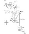
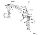
図1は、本実施形態の表示装置100の外観の一態様を示す外観図である。図2は、図1に示す表示装置100の光学系10の一態様を示す説明図である。なお、図1および図2においては、表示装置を装着した観察者に対する前後方向をZ軸に沿う方向とし、前後方向の一方側として表示装置を装着した観察者の前方を前側Z1とし、前後方向の他方側として表示装置を装着した観察者の後方を後側Z2としてある。また、表示装置を装着した観察者に対する左右方向をX軸に沿う方向とし、左右方向の一方側として表示装置を装着した観察者の右方を右側X1とし、左右方向の他方側として表示装置を装着した観察者の左方を左側X2としてある。また、表示装置を装着した観察者に対する上下方向をY軸方向に沿う方向とし、上下方向の一方側として表示装置を装着した観察者の上方を上側Y1とし、上下方向の他方側として表示装置を装着した観察者の下方を下側Y2としてある。 FIG. 1 is an external view showing one aspect of the external appearance of the
図1に示す表示装置100は、頭部装着型の表示装置であり、画像光L0aを右眼Eaに入射させる右眼用光学系10aと、画像光L0bを左眼Ebに入射させる左眼用光学系10bとを有している。表示装置100は、例えば、眼鏡のような形状に形成される。具体的に、表示装置100は、右眼用光学系10aと左眼用光学系10bとを保持する筐体90をさらに備えている。表示装置100は、筐体90によって観察者の頭部に装着される。 The
表示装置100は、筐体90として、フレーム91と、フレーム91の右側に設けられ、観察者の右耳に係止されるテンプル92aと、フレーム91の左側に設けられ、観察者の左耳に係止されるテンプル92bと、を備えている。フレーム91は、両側部に収納空間91sを有しており、収納空間91s内に、後述する光学系10を構成する画像光投射装置等の各部品が収容されている。テンプル92a,92bは、ヒンジ95によってフレーム91に対して折り畳み可能に連結されている。 The
右眼用光学系10aと左眼用光学系10bとは基本的な構成が同一である。従って、以下の説明では、右眼用光学系10aと左眼用光学系10bとを区別せずに光学系10として説明する。 The optical system for
また、図1に示す表示装置100では、画像光L0をX軸に沿う左右方向に進行させている。 Further, in the
図2を参照して表示装置100の光学系10の基本的な構成を説明する。図2では、画像光L0の特定波長の光L1(実線)に加えて、長波長側の光L2(一点鎖線)、および特定波長に対して短波長側の光L3(点線)も図示してある。 A basic configuration of the
図2に示すように、光学系10では、画像光生成装置31から出射された画像光L0の進行方向に沿って、正のパワーを有する第1光学部L10と、ミラー40と、正のパワーを有する第2光学部L20と、正のパワーを有する第3光学部L30と、正のパワーを有する第4光学部L40とが配置されている。 As shown in FIG. 2, in the
本実施形態において、正のパワーを有する第1光学部L10は、投射光学系32によって構成されている。正のパワーを有する第2光学部L20は、反射型の第1回折素子50によって構成されている。正のパワーを有する第3光学部L30は、導光系60によって構成されている。正のパワーを有する第4光学部L40は、反射型の第2回折素子70によって構成されている。本実施形態において、第1回折素子50および第2回折素子70は、反射型の回折素子である。 In this embodiment, the first optical section L10 having positive power is configured by the projection
ミラー40は、反射面400が凹曲面になっており、正のパワーを有している。ミラー40の反射面400が正のパワーを有する場合、ミラー40を投射光学系32の構成要素に含めるようにしてもよい。すなわち、ミラー40が正のパワーを有する場合、第1光学部L10がミラー40を含むようにしてもよい。なお、ミラー40の反射面400が、平面になっており、パワーを有しないように構成してもよい。 The
かかる光学系10において、画像光L0の進行方向に着目すると、画像光生成装置31は、投射光学系32に向けて画像光L0を出射し、投射光学系32は入射した画像光L0をミラー40に向けて出射する。ミラー40は入射した画像光L0を第1回折素子50に向けて反射し、第1回折素子50は入射した画像光L0を導光系60に向けて出射する。導光系60は、入射した画像光L0を第2回折素子70に出射し、第2回折素子70は、入射した画像光L0を観察者の眼Eに向けて出射する。 Focusing on the traveling direction of the image light L0 in the
本実施形態において、画像光生成装置31は画像光L0を生成する。
画像光生成装置31は、有機エレクトロルミネッセンス表示素子等の表示パネル310を備えている態様を採用することができる。かかる態様によれば、小型で高画質な画像表示が可能な表示装置100を提供することができる。また、画像光生成装置31は、照明光源(図示せず)と、照明光源から出射された照明光を変調する液晶表示素子等の表示パネル310とを備えている態様を採用してもよい。かかる態様によれば、照明光源の選択が可能なため、画像光L0の波長特性の自由度が広がるという利点がある。ここで、画像光生成装置31は、カラー表示可能な1枚の表示パネル310を有する態様を採用することができる。また、画像光生成装置31は、各色に対応する複数の表示パネル310と、複数の表示パネル310から出射された各色の画像光を合成する合成光学系とを有する態様を採用してもよい。さらに、画像光生成装置31は、レーザー光をマイクロミラーデバイスで変調する態様を採用してもよい。In this embodiment, the
The image
投射光学系32は画像光生成装置31が生成した画像光L0を投射する光学系であって、複数のレンズ321によって構成されている。図2では、投射光学系32におけるレンズ321を3枚とした場合を例に挙げたが、レンズ321の枚数はこれに限定されることはなく、投射光学系32が4枚以上のレンズ321を備えていてもよい。また、各レンズ321は貼り合わせて投射光学系32を構成してもよい。また、レンズ321は自由曲面のレンズで構成されていてもよい。 The projection
導光系60は、第1回折素子50から出射された画像光L0が入射するレンズ系61と、レンズ系61から出射された画像光L0を斜めに傾いた方向に出射するミラー62とを有している。レンズ系61は、Z軸に沿う前後方向に配置された複数のレンズ611からなる。ミラー62は、前後方向に向けて斜めに傾いた反射面620を有している。本実施形態において、ミラー62は全反射ミラーである。但し、ミラー62をハーフミラーとしてもよく、この場合、外光を視認できる範囲を広くすることができる。 The
続いて、第1回折素子50および第2回折素子70の構成について説明する。
本実施形態において、第1回折素子50および第2回折素子70は基本的な構成が同一である。以下では、第2回折素子70の構成を例に挙げて説明する。Next, configurations of the
In this embodiment, the
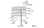
図3Aは、図2に示す第2回折素子70の干渉縞751の説明図である。図3Aに示すように、第2回折素子70は、反射型体積ホログラフィック素子75を備えており、反射型体積ホログラフィック素子75は部分反射型回折光学素子である。このため、第2回折素子70は、部分透過反射性のコンバイナーを構成している。従って、外光も第2回折素子70を介して眼Eに入射するため、観察者は、画像光生成装置31で形成した画像光L0と外光(背景)とが重畳した画像を認識することができる。 FIG. 3A is an explanatory diagram of
第2回折素子70は、観察者の眼Eと対向しており、画像光L0が入射する第2回折素子70の入射面71は、眼Eから離れる方向に凹んだ凹曲面になっている。換言すれば、入射面71は、画像光L0の入射方向において、周辺部に対して中央部が凹んで湾曲した形状となっている。このため、画像光L0を観察者の眼Eに向けて効率良く集光させることができる。 The
第2回折素子70は、特定波長に対応するピッチを有した干渉縞751を有している。干渉縞751は屈折率等の差としてホログラム感光層に記録されており、干渉縞751は特定の入射角度に対応するように、第2回折素子70の入射面71に対して一方方向に傾いている。従って、第2回折素子70は、画像光L0を所定の方向に回折して偏向する。特定波長および特定の入射角度とは、画像光L0の波長と入射角度に対応する。かかる構成の干渉縞751は、参照光Lrおよび物体光Lsを用いてホログラフィック感光層に干渉露光を行うことにより形成することができる。 The
本実施形態では、画像光L0がカラー表示用である。このため、第2回折素子70は、特定波長に対応するピッチで形成された干渉縞751R、751G、751Bを有している。例えば、干渉縞751Rは、580nmから700nmの波長範囲のうち、例えば、波長615nmの赤色光LRに対応するピッチで形成される。干渉縞751Gは、500nmから580nmの波長範囲のうち、例えば、波長535nmの緑色光LGに対応するピッチで形成される。干渉縞751Bは、400nmから500nmの波長範囲のうち、例えば、波長460nmの青色光LBに対応するピッチで形成される。かかる構成は、各波長に対応する感度を有するホログラフィック感光層を形成した状態で、各波長の参照光LrR、LrG、LrB、および物体光LsR、LsG、LsBを用いてホログラフィック感光層に干渉露光を行うことにより形成することができる。 In this embodiment, the image light L0 is for color display. Therefore, the
なお、各波長に対応する感度を有する感光材料をホログラフィック感光層に分散させておき、各波長の参照光LrR、LrG、LrBおよび物体光LsR、LsG、LsBを用いてホログラフィック感光層に干渉露光を行うことによって、図3Bに示すように1つの層に干渉縞751R、751G、751Bを重畳した干渉縞751を形成してもよい。また、参照光LrR、LrG、LrBおよび物体光LsR、LsG、LsBとして球面波の光を用いてもよい。 A photosensitive material having a sensitivity corresponding to each wavelength is dispersed in the holographic photosensitive layer, and the reference beams LrR, LrG, and LrB and the object beams LsR, LsG, and LsB of each wavelength are used to interfere with the holographic photosensitive layer. By performing exposure, as shown in FIG. 3B,
第2回折素子70と基本的な構成が同一である第1回折素子50は、反射型体積ホログラフィック素子55を備えている。第1回折素子50は、画像光L0が入射する入射面51が、凹んだ凹曲面になっている。換言すれば、入射面51は、画像光L0の入射方向において、周辺部に対して中央部が凹んで湾曲した形状となっている。そのため、画像光L0を導光系60に向けて効率良く偏向させることができる。 The first
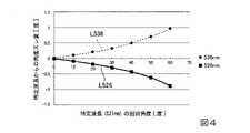
図4は、図2に示す第1回折素子50および第2回折素子70の回折特性を示す説明図である。図4は、体積ホログラム上の1点に光線が入射したときの、特定波長と周辺波長の回折角の差を示したものである。図4には、特定波長を531nmとしたとき、波長が526nmの周辺波長の光の回折角度のずれを実線L526で示し、波長が536nmの周辺波長の光の回折角度のずれを点線L536で示してある。 FIG. 4 is an explanatory diagram showing diffraction characteristics of the
図4に示すように、ホログラムに記録された同じ干渉縞に光線が入射した場合でも、長波長の光線程、大きく回折し、短波長の光線程、回折しにくい。そのため、本実施形態のように2つの回折素子、すなわち第1回折素子50および第2回折素子70を用いた際、特定波長に対する長波長の光および短波長の光における光線角度をそれぞれ考慮して入射させないと適正に波長補償できない。すなわち第2回折素子70で発生する色収差をキャンセルできなくなる。また、干渉縞の本数によって回折角が異なるので、干渉縞を考慮する必要がある。 As shown in FIG. 4, even when light rays are incident on the same interference fringes recorded in the hologram, light rays with longer wavelengths are diffracted more, and light rays with shorter wavelengths are less diffracted. Therefore, when two diffraction elements, that is, the
ところで、第1回折素子50および第2回折素子70は図3Aおよび図3Bに示したように2光束干渉露光で形成されたホログラフィック素子で構成される。このように2光束干渉露光で形成されたホログラフィック素子は、干渉縞が形成された面内における回折力が強く、光を曲げる偏向力が強い。なお、干渉縞が形成された面とは、図3Aおよび図3Bの紙面に沿う面に相当する。以下の説明において、干渉縞が形成された面を主回折面と呼ぶことにする。図2に示した光学系10では、XZ面に平行な面に沿って画像光L0を大きく偏向させることで観察者の眼Eに導いている。本実施形態の光学系10において、主回折面は図2に示すXZ面と平行な面で規定される。 By the way, the
一方、2光束干渉露光で形成されたホログラフィック素子において、主回折面に垂直な面内における回折力が弱く、光を曲げる偏向力が弱い。ここで、主回折面に垂直な面とは、図3Aおよび図3Bの紙面に垂直な面に相当し、以下の説明において、この面を副回折面と呼ぶことにする。本実施形態の光学系10において、副回折面とは図2に示すXZ面に直交する面、すなわち図2の紙面に垂直な面である。 On the other hand, in a holographic element formed by two-beam interference exposure, the diffraction power in the plane perpendicular to the main diffraction plane is weak, and the deflection power for bending light is weak. Here, the plane perpendicular to the main diffraction plane corresponds to the plane perpendicular to the paper surface of FIGS. 3A and 3B, and in the following description, this plane will be called the sub-diffraction plane. In the
すなわち、2光束干渉露光で形成された第1回折素子50および第2回折素子70では、主回折面内の回折角度に比べて、副回折面内の回折角度が小さい。図4を用いて説明したように、回折角度が小さくなるほど、周辺波長における特定波長からの回折角度のずれが小さくてすむ。なお、主回折面と副回折面との間に存在する面内においても光の回折は生じているが、本明細書では最大の回折角度を生じる主回折面と最低の回折角度を生じる副回折面とについて考える。 That is, in the
ここで、第1回折素子50および第2回折素子70について、主回折面および副回折面間で生じる回折角度差を考慮しないで設計する場合について考える。この場合、第1光学部L10、第2光学部L20、第3光学部L30および第4光学部L40は主回折面および副回折面の両方とも同様のパワーを有するように設計される。 Consider a case where the
上述したように副回折面内で生じる周辺波長の回折角度差は小さいことから、主回折面内で生じる回折角度差を補償するために必要となる各光学部のパワーは、副回折面内で生じる回折角度差を補償するために必要となる各光学部のパワーより高くなる。
従って、主回折面および副回折面間で生じる回折角度差を考慮しないで各光学部を設計した場合、各光学部において副回折面内におけるパワーは余剰となってしまう。そのため、組立公差が必要以上に厳しくなるという問題が生じる。As described above, since the diffraction angle difference of the peripheral wavelengths occurring in the sub-diffraction plane is small, the power of each optical section required to compensate for the diffraction angle difference occurring in the main diffraction plane is It is higher than the power of each optical section required to compensate for the diffraction angle difference that occurs.
Therefore, if each optical section is designed without considering the diffraction angle difference between the main diffraction plane and the sub-diffraction plane, the power in the sub-diffraction plane in each optical section becomes redundant. Therefore, there arises a problem that the assembly tolerance becomes stricter than necessary.
本発明者は、副回折面内で生じる周辺波長の回折角度差は小さいため、回折角度差に起因する画像光の角度ずれはレンズで生じる分散で概ね補正可能と考えた。そして、本実施形態の光学系10の構成を見出した。 The present inventor thought that since the diffraction angle difference of the peripheral wavelengths occurring in the sub-diffraction plane is small, the angle shift of the image light caused by the diffraction angle difference can be corrected by the dispersion occurring in the lens. Then, the configuration of the
本実施形態の光学系10では、画像光L0の光路において、画像光L0の主回折面内における偏向力が副回折面内における偏向力よりも大きくしている。画像光L0の偏向力は第1光学部L10、第2光学部L20、第3光学部L30および第4光学部L40のパワーに依存する。すなわち、本実施形態の光学系10では、第1光学部L10、第2光学部L20、第3光学部L30および第4光学部L40において、主回折面内におけるパワーよりも副回折面内におけるパワーを小さくした。 In the
図2に示す光学系10では、少なくとも図2に示した主回折面としてのXZ面において、特開2017-167181号公報に記載されているように、第1回折素子50と第2回折素子70との間での中間像の形成回数と、ミラー62での反射回数の和が奇数か偶数かに対応して、第2回折素子70への入射方向等を適正化してある。そのため、少なくとも主回折面に沿う面内において、画像光の波長補償、すなわち色収差をキャンセル可能である。 In the
具体的に、第1回折素子50に入射した画像光L0は、図2に示すように、主回折面内において、第1回折素子50によって回折されることで偏向する。このとき、特定波長に対して長波長側の光L2の回折角度θ2は、特定波長の光L1の回折角度θ1より大きくなる。また、特定波長に対して短波長側の光L3の回折角度θ3は、特定波長の光L1の回折角度θ1より小さくなる。従って、第1回折素子50を出射した画像光L0は、波長毎に偏向されて分散することとなる。Specifically, the image light L0 incident on the
第1回折素子50を出射した画像光L0は、導光系60を介して第2回折素子70に入射し、第2回折素子70によって回折されることで偏向する。その際、第1回折素子50から第2回折素子70までの光路において、中間像の形成が1回行われるとともに、ミラー62での反射が1回行われる。従って、画像光L0と第2回折素子70の入射面法線との間の角度を入射角とすると、特定波長に対して長波長側の光L2は、特定波長の光L1における入射角θ11よりも大きな入射角θ12となり、特定波長に対して短波長側の光L3は、特定波長の光L1における入射角θ11よりも小さな入射角θ13となる。また、上述したように特定波長に対して長波長側の光L2の回折角度θ2は、特定波長の光L1の回折角度θ1よりも大きくなり、特定波長に対して短波長側の光L3の回折角度θ3は、特定波長の光L1の回折角度θ1よりも小さくなる。The image light L0 emitted from the
従って、特定波長に対して長波長側の光L2は、特定波長の光L1よりも大きな入射角で第1回折素子50に入射するが、特定波長に対して長波長側の光L2の回折角度が、特定波長の光L1の回折角度よりも大きいため、結果として第2回折素子70から出射するときには、特定波長に対して長波長側の光L2と特定波長の光L1は略平行な光となる。これに対して、特定波長に対して短波長側の光L3は、特定波長の光L1よりも小さな入射角で第1回折素子50に入射するが、特定波長に対して短波長側の光L3の回折角度が、特定波長の光L1の回折角度よりも小さいため、結果として第2回折素子70から出射するときには、特定波長に対して短波長側の光L3と特定波長の光L1は略平行な光となる。このようにして、図2に示すように、第2回折素子70を出射した画像光L0は、略平行な光として観察者の眼Eに入射するので、波長毎の網膜E0での結像位置ずれが抑制される。従って、図2に示した主回折面内において、第2回折素子70で発生する画像光L0の色収差をキャンセルできる。 Therefore, the light L2 on the long wavelength side with respect to the specific wavelength is incident on the
続いて、第1回折素子50と第2回折素子70との共役関係について説明する。本実施形態の光学系10において、第1回折素子50および第2回折素子70は、少なくとも図2に示した主回折面内において後述する共役関係が成立している。 Next, the conjugate relationship between the
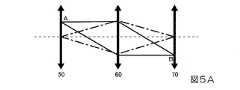
図5Aは、第1回折素子50と第2回折素子70とが共役関係にある場合の説明図である。図5Bおよび図5Cは第1回折素子50と第2回折素子70とが共役関係にない場合の説明図である。図6Aおよび図6Bは、図5Bおよび図5Cに示す第1回折素子50と第2回折素子70との共役関係からのずれの許容差を示す説明図である。図6Aおよび図6Bには、特定波長の光を実線Leで示し、波長が特定波長-10nmの光を一点鎖線Lfで示し、波長が特定波長+10nmの光を二点鎖線Lgで示してある。なお、図5A~Cおよび図6Aおよび図6Bでは、光の進行が分かりやすいように、第1回折素子50、第2回折素子70および導光系60を透過型として示し、第1回折素子50、第2回折素子70および導光系60を矢印で示してある。 FIG. 5A is an explanatory diagram when the
図5Aに示すように、第1回折素子50と第2回折素子70とを共役の関係とした場合、第1回折素子50のA点から出射した発散光は正パワーを持つ導光系60によって集光され、第2回折素子70のB点に入射する。従って、B点で発生する回折による色収差をA点で補償することができる。 As shown in FIG. 5A, when the
これに対して、図5Bおよび図5Cに示すように、第1回折素子50と第2回折素子70とが共役の関係にない場合、第1回折素子50のA点から出射した発散光は、中央の正パワーを持つ導光系60によって集光されるが、第2回折素子70上のB点よりも遠い位置、あるいは近い位置で交わって入射する。このため、A点とB点とが1対1の関係になっていない。ここで、領域内の干渉縞が一様の場合に補償効果が高まることから、第1回折素子50と第2回折素子70とが共役の関係にない場合、補償効果が弱くなる。一方、第1回折素子50によって、第2回折素子70の投影領域全体を補償することは困難である。それ故、図5Bおよび図5Cに示す態様の場合、十分な波長補償を行うことができないので、解像度の劣化が発生する。 On the other hand, as shown in FIGS. 5B and 5C, when the
なお、特定波長に対して±10nmの波長の光では、特定波長の光が到達するB点から±0.4mm程度の誤差が存在するが、解像度の低下は目立たない。かかる許容範囲を検討した結果、図6Aに示すように、特定波長の光が到達する理想的な第2回折素子70上のB点よりも手前で交わり±0.8mmの範囲内に入射する場合には、解像度の低下は目立たない。また、図6Bに示すように、特定波長の光が到達する理想的な第2回折素子70上のB点よりも後方で交わり±0.8mmの範囲内に入射する場合には、解像度の低下は目立たない。従って、第1回折素子50と第2回折素子70とにおいては、完全な共役関係になくても、略共役関係にあって、理想的なB点から±0.8mmの範囲内に到達する場合には、解像度の低下を許容することができる。すなわち、本実施形態において、第1回折素子50と第2回折素子70とが共役関係を有するとは、特定波長の光の入射位置が理想的な入射点から±0.8mmの誤差範囲に収まることをいう。 In the case of light with a wavelength of ±10 nm with respect to the specific wavelength, there is an error of about ±0.4 mm from the point B where the light with the specific wavelength reaches, but the decrease in resolution is not conspicuous. As a result of examining such an allowable range, as shown in FIG. 6A, when light of a specific wavelength intersects in front of the ideal point B on the
図7Aは光学系10の主回折面における光線図である。図7Bは光学系10の副回折面における光線図である。図7A、図7Bおよび後で参照する図では、光軸に沿って配置された各光学部を太い矢印で示してある。なお、光軸に沿って配置された各光学部を矢印ではなく太線のみで示す場合は光学部がパワーを有していないことを意味する。
また、画像光生成装置31の1つの画素から出射した光線を実線Laで示し、画像光生成装置31の端部から出射される主光線を一点鎖線Lbで示し、第1回折素子50と共役関係となる位置を長い破線Lcで示してある。ここで、「中間像」とは、1画素から出射された光線(実線La)が集まる個所であり、「瞳」とは、各画角の主光線(一点鎖線Lb)が集まる個所である。また、図7Aおよび図7Bは、画像光生成装置31から出射された光の進行を示すものである。なお、図7Aおよび図7Bにおいては、図を簡略化するため、すべての光学部を透過型として図示している。FIG. 7A is a ray diagram in the main diffraction plane of the
Further, a light ray emitted from one pixel of the image
図7Aに示すように、光学系10は、主回折面内において、第1光学部L10の焦点距離FがL/2であり、第2光学部L20、第3光学部L30、および第4光学部L40の焦点距離FがいずれもLである。 As shown in FIG. 7A, in the
一方、図7Bに示すように、光学系10は、副回折面内において、第1光学部L10の焦点距離FがLであり、第2光学部L20および第4光学部L40の焦点距離Fがいずれも2Lである。光学系10は、副回折面内において、太線で示された第3光学部L30を有している。すなわち、副回折面内において、第3光学部L30は主回折面と比べ中間像や瞳を形成するパワーを有していない。ここで、第3光学部L30がパワーを有していないとは、第3光学部L30を構成するレンズが副回折面内においてレンズ面を有さない板状であることを意味する。 On the other hand, as shown in FIG. 7B, in the
また、本実施形態の光学系10は、主回折面と副回折面とを比べた場合、副回折面内における第1光学部L10、第2光学部L20および第4光学部L40の焦点距離Fが長くなっている。このように本実施形態の光学系10では、副回折面内において、第3光学部L30の焦点距離Fを長くし、パワーを無くすことで、主回折面内におけるパワーよりも副回折面内におけるパワーを小さくしている。このようにして本実施形態の光学系10は、画像光の主回折面内における偏向力を副回折面内における偏向力よりも大きくしている。 In the
図8は本実施形態の光学系10において形成される画像光の中間像の状態を示す図である。図8は本実施形態の光学系10に対応するモデルを用いたシミュレーションにより算出され、主回折面内に形成される中間像と副回折面内に形成される中間像とを示している。 FIG. 8 is a diagram showing the state of an intermediate image of image light formed in the
図7Aおよび図8に示すように、本実施形態の光学系10は主回折面内において、第1光学部L10と第3光学部L30との間に画像光の第1中間像P1が形成され、第3光学部L30と第4光学部L40との間に画像光の第2中間像P2が形成される。すなわち、本実施形態の光学系10では、主回折面上に形成される中間像の数が2つである。 As shown in FIGS. 7A and 8, in the
一方、図7Bおよび図8に示すように、本実施形態の光学系10は副回折面内において、第2光学部L20と第4光学部L40との間に画像光の中間像Pが形成される。すなわち、本実施形態の光学系10では、主回折面上に形成される中間像の数が1つである。そのため、本実施形態の光学系10では、主回折面上に形成される画像光の中間像の数が副回折面上に形成される画像光の中間像の数よりも多い。 On the other hand, as shown in FIGS. 7B and 8, in the
また、第3光学部L30は、画像光生成装置31の1点からの画像光について、第1回折素子50により偏向されて特定波長からずれた周辺波長の光を第2回折素子70の所定の範囲に入射させる。すなわち、第1回折素子50と第2回折素子70は共役あるいは略共役の関係にある。ここで、第1回折素子50の第3光学部L30による第2回折素子70上の射影の倍率の絶対値は0.5倍から10倍までであり、かかる倍率の絶対値は1倍から5倍までであることが好ましい。 In addition, the third optical unit L30 converts the image light from one point of the image
図9は本実施形態の光学系10における瞳の関係を示す図である。図9は本実施形態の光学系10に対応するモデルを用いたシミュレーションにより算出され、主回折面内における瞳と副回折面内における瞳とを示している。 FIG. 9 is a diagram showing the relationship of pupils in the
図7Aおよび図9に示すように、本実施形態の光学系10は主回折面内において、第1光学部L10内に瞳R0が形成され、第2光学部L20と第4光学部L40との間に瞳R1が形成され、第4光学部L40は、画像光を平行光化して射出瞳R2を形成する。瞳R1は、第2光学部L2と第4光学部L40との間のうち、第3光学部L30の近傍に形成される。第3光学部L30の近傍とは、第2光学部L20と第3光学部L30の間のうち、第2光学部L20より第3光学部L30に近い位置、または第3光学部L30と第4光学部L40の間のうち、第4光学部L40より第3光学部L30に近い位置を意味する。すなわち、本実施形態の光学系10では、主回折面内における瞳の数が2つである。 As shown in FIGS. 7A and 9, in the
一方、図7Bおよび図9に示すように、本実施形態の光学系10は副回折面内において、第1光学部L10内に瞳R0が形成され、第4光学部L40が画像光を平行光化することで射出瞳R2のみを形成する。すなわち、本実施形態の光学系10は、副回折面内における瞳の数が1つである。そのため、本実施形態の光学系10は、主回折面上に形成される瞳の数が副回折面上に形成される瞳の数よりも多い。 On the other hand, as shown in FIGS. 7B and 9, in the
従って、本実施形態の光学系10によれば、主回折面内において、投射光学系32と導光系60との間に画像光の第1中間像P1が形成され、導光系60の近傍に瞳R1が形成され、導光系60と第2回折素子70との間に画像光の第2中間像P2が形成され、第2回折素子70は、画像光を平行光化して射出瞳R2を形成する。 Therefore, according to the
本実施形態の光学系10において、第1中間像P1は、第1光学部L10(投射光学系32)と第2光学部L20(第1回折素子50)との間に形成される。 In the
本実施形態の光学系10によれば、主回折面内において、以下に示す4つの条件(条件1、2、3、4)を満たしている。
条件1:画像光生成装置31の1つの点から出射した光線は、網膜E0に1つの点として結像される。
条件2:光学系の入射瞳と眼球の瞳が共役である。
条件3:周辺波長を補償するように第1回折素子50と第2回折素子70とを適正に配置する。
条件4:第1回折素子50と第2回折素子70とが共役または略共役の関係にある。According to the
Condition 1: A light ray emitted from one point of the image
Condition 2: The entrance pupil of the optical system and the pupil of the eyeball are conjugate.
Condition 3: Properly arrange the
Condition 4: The
より具体的には、図7Aに示した一点鎖線Lbから分かるように、画像光生成装置31の1つの点から出射した光線は、網膜E0に1つの点として結像されるという条件1を満たすので、観察者は1画素を視認することができる。また、図7Aに示した実線Laから分かるように、光学系10の入射瞳と眼Eの瞳E1とが共役(瞳の共役)の関係にあるという条件2を満たすので、画像光生成装置31で生成した画像の全域を視認することができる。また、周辺波長を補償するように第1回折素子50と第2回折素子70とを適正に配置するという条件3を満たすため、波長補償を行うことによって第2回折素子70で発生する色収差をキャンセル可能である。また、図7Aに示した長い破線Lcから分かるように、第1回折素子50と第2回折素子70とが共役または略共役の関係にあるという条件4を満たすため、第1回折素子50と第2回折素子70とでは、光線を干渉縞が同一な個所に入射させることが可能であり、波長補償を適正に行うことができる。よって、画像光の解像度の劣化を抑えることができる。 More specifically, as can be seen from the dashed-dotted line Lb shown in FIG. 7A, a light ray emitted from one point of the image
本実施形態の光学系10では、副回折面内において、上述した4つの条件のうち、少なくとも第1条件および第2条件を満たしている。より具体的に、図7Bに示した一点鎖線Lbから分かるように、画像光生成装置31の1つの点から出射した光線は、網膜E0に1つの点として結像されるという条件1を満たすので、観察者は1画素を視認することができる。また、図7Bに示した実線Laから分かるように、光学系10の入射瞳と眼Eの瞳E1とが共役(瞳の共役)の関係にあるという条件2を満たすので、画像光生成装置31で生成した画像の全域を視認することができる。 In the
一方、本実施形態の光学系10では、画像光の主回折面内における偏向力より副回折面内における偏向力を小さくしたため、副回折面内において上述の条件3および条件4を満たさなくなる。
ここで、上述したように副回折面内で生じる周辺波長の回折角度差は小さい。そのため、副回折面内において条件3および条件4を満たさないとしても、第1回折素子50により偏向された際に生じる特定波長の回折角度差が小さいので、回折角度差によってずれた光を光学部のレンズで生じる分散によって補正して第2回折素子70の所定の範囲に入射させることができる。このため、干渉縞が異なる場所に入射するという問題が生じたとしても影響を最小限に抑えることができる。On the other hand, in the
Here, as described above, the diffraction angle difference of the peripheral wavelengths occurring within the sub-diffraction plane is small. Therefore, even if conditions 3 and 4 are not satisfied in the sub-diffraction plane, the diffraction angle difference of the specific wavelength generated when deflected by the
従って、本実施形態の光学系10では、副回折面内においても特定波長の周辺波長の光を特定波長の光の近傍に概ね入射可能となるので、条件3および条件4を満たさない場合でも、色収差の発生を概ねキャンセルできる。よって、本実施形態の光学系10は、副回折面内においても解像度の劣化を抑えることができる。すなわち、本実施形態の光学系10によれば、主回折面に比べて波長補償効果は弱いものの、開口率が小さい場合や観察者の眼に入射する光線径(射出瞳径)が小さい場合は一定の波長補償効果を得ることができる。 Therefore, in the
また、本実施形態の光学系10では、画像光の光路において、画像光L0の主回折面内における偏向力が副回折面内における偏向力よりも大きくなっている。また、本実施形態の光学系10では、主回折面上に形成される画像光の中間像および瞳の数が、副回折面上に形成される前記画像光の中間像および瞳の数よりも多くなっている。
すなわち、本実施形態の光学系10は、第1回折素子50および第2回折素子70において主回折面および副回折面間で生じる回折角度差を考慮して各光学部のパワーを設計している。そのため、副回折面内における各光学部のパワーが必要以上に強くなることを低減することができる。
従って、本実施形態の光学系10によれば、副回折面内において各光学部のパワーが抑えられるので、各光学部を構成するレンズなどの光学部品の組立公差を緩和することができる。Further, in the
That is, in the
Therefore, according to the
(第二実施形態)
続いて、第二実施形態に係る光学系の構成について説明する。
本実施形態の光学系は、主回折面内において第一実施形態の光学系10と同じパワーを有するが、副回折面内におけるパワーが第一実施形態の光学系10と異なっている。以下の説明では、第一実施形態と共通の構成については同じ符号を付し、その説明については省略する。(Second embodiment)
Next, the configuration of the optical system according to the second embodiment will be explained.
The optical system of this embodiment has the same power in the main diffraction plane as the
図10は本実施形態の光学系の副回折面内における光線図である。なお、本実施形態の光学系の主回折面における光線図は図7Aと共通であるため、省略する。
図10に示すように、本実施形態の光学系10Aは、副回折面内において、第1光学部L10の焦点距離FがLであり、第2光学部L20および第4光学部L40の焦点距離FがいずれもLであり、第3光学部L30の焦点距離FがL/2である。FIG. 10 is a ray diagram in the sub-diffractive plane of the optical system of this embodiment. Note that the ray diagram on the main diffraction surface of the optical system of this embodiment is the same as in FIG. 7A, so it is omitted.
As shown in FIG. 10, in the
一方、本実施形態の光学系10Aでは、主回折面内において、第1光学部L10の焦点距離FがL/2であり、第2光学部L20、第3光学部L30、および第4光学部L40の焦点距離FがいずれもLである(図7A参照)。 On the other hand, in the
本実施形態の光学系10Aでは、主回折面と副回折面とを比べた場合、副回折面内において第1光学部L10の焦点距離Fを長くしている。すなわち、本実施形態の光学系10Aは、第1光学部L10における副回折面内でのパワーを抑えた構成を採用している。 In the
このように本実施形態の光学系10Aでは、副回折面内において、第1光学部L10のパワーを抑えて焦点距離Fを長くすることで、主回折面内におけるパワーよりも副回折面内におけるパワーを小さくしている。このようにして本実施形態の光学系10Aでは、画像光の主回折面内における偏向力を副回折面内における偏向力よりも大きくしている。 As described above, in the
本実施形態の光学系10Aでは、図7Aに示したように主回折面内において、第1光学部L10と第3光学部L30との間に画像光の第1中間像P1が形成され、第3光学部L30と第4光学部L40との間に画像光の第2中間像P2が形成される。より具体的に、第1中間像P1は、第1光学部L10と第2光学部L20との間に形成される。よって、第1中間像P1と第2中間像P2との距離は図7Aに示す符号H1で規定される。 In the
一方、本実施形態の光学系10Aでは、図8に示したように副回折面内において、第1光学部L10と第3光学部L30との間に画像光の第1中間像P1が形成され、第3光学部L30と第4光学部L40との間に画像光の第2中間像P2が形成される。より具体的に、第1中間像P1は、第2光学部L20と第2光学部L20との間に形成される。よって、第1中間像P1と第2中間像P2との距離は図8に示す符号H2で規定される。 On the other hand, in the
従って、本実施形態の光学系10Aでは、主回折面の光線図と副回折面の光線図とを比べた場合、主回折面上に形成される第1中間像P1および第2中間像P2間の第1の距離H1が、副回折面上に形成される第1中間像P1および第2中間像P2間の第2の距離H2よりも長くなっている。 Therefore, in the
本実施形態の光学系10Aでは、第1の距離H1を第2の距離H2よりも長くしたことで、画像光の主回折面内における偏向力より副回折面内における偏向力を小さくする構成を採用している。
本実施形態の光学系10Aでは、第一実施形態の光学系10と同様、第1回折素子50および第2回折素子70において主回折面および副回折面間で生じる回折角度差を考慮して各光学部のパワーを設計している。そのため、副回折面内における各光学部のパワーが必要以上に強くなることを低減することができる。従って、本実施形態の光学系10Aにおいても、回折面内において各光学部のパワーが抑えられるので、各光学部を構成するレンズなどの光学部品の組立公差を緩和することができる。In the
In the
本実施形態の光学系10Aにおいても、第一実施形態の構成と同様、主回折面内において、4つの条件を満たすため、第1回折素子50と第2回折素子70とでは、光線を干渉縞が同一な個所に入射させることが可能であり、波長補償を適正に行うことで色収差をキャンセルできる。よって、画像光の解像度の劣化を抑えることができる。
また、副回折面内においては上述の条件3および条件4を満たさなくなるが、副回折面内で生じる周辺波長の回折角度差は小さいことから、本実施形態の光学系10Aにおいても副回折面内にて特定波長の周辺波長の光を特定波長の光の近傍に概ね入射させることで色収差の発生を概ねキャンセル可能となる。Also in the
In addition, although the above conditions 3 and 4 are not satisfied within the sub-diffraction plane, the diffraction angle difference of the peripheral wavelengths occurring within the sub-diffraction plane is small. By causing the light of the peripheral wavelength of the specific wavelength to enter the vicinity of the light of the specific wavelength, the occurrence of chromatic aberration can be substantially canceled.
(第三実施形態)
続いて、第三実施形態に係る光学系の構成について説明する。本実施形態の光学系は、画像光生成装置の構成が第一実施形態と異なっている。以下の説明では、第一実施形態と共通の構成については同じ符号を付し、その説明については省略する。(Third embodiment)
Next, the configuration of the optical system according to the third embodiment will be explained. The optical system of this embodiment differs from that of the first embodiment in the configuration of the image light generating device. In the following description, the same reference numerals are given to the configurations common to the first embodiment, and the description thereof will be omitted.
図11は、第三実施形態に係る光学系10Bの光線図である。なお、図11は主回折面での光学系の構成を示している。図11に示すように、本実施形態の光学系10Bでは、第一実施形態の構成と同様、正のパワーを有する第1光学部L10と、第1回折素子50を含み、正のパワーを有する第2光学部L20と、正のパワーを有する第3光学部L30と、反射型の第2回折素子70を含み、正のパワーを有する第4光学部L40とが設けられている。 FIG. 11 is a ray diagram of the
本実施形態の画像光生成装置31は、レーザー光源316と、コリメートレンズ317と、マイクロミラーデバイス318とを有しており、マイクロミラーデバイス318を駆動することによりレーザー光源316を走査することにより、画像を生成する。従って、本実施形態においては、画像光生成装置31自身が画角の光を形成する。 The image
本実施形態の光学系10Bを搭載した表示装置によれば、観察者の装着に、体温や表示装置自身の熱によって温度変化が発生してレーザー光のスペクトラム幅等が変動した場合でも、波長補償によって品位の高い画像を表示することができる。 According to the display device equipped with the
(第四実施形態)
続いて、第四実施形態について説明する。本実施形態は表示装置の別の形態に関するものである。なお、以下の説明では、第一実施形態と共通の構成については同じ符号を付し、その説明については省略する。(Fourth embodiment)
Next, a fourth embodiment will be described. This embodiment relates to another form of the display device. In addition, in the following description, the same code|symbol is attached|subjected about the structure common to 1st embodiment, and it abbreviate|omits about the description.
図12は第四実施形態に係る表示装置の説明図である。図12は主回折面での光学系の構成を示しており、図12におけるXYZで示す方向は図1および図2における方向に一致する。
図12に示すように、本実施形態の表示装置101は、画像光を上側Y1から下側Y2に進行させて観察者の眼Eに出射させる。FIG. 12 is an explanatory diagram of the display device according to the fourth embodiment. FIG. 12 shows the configuration of the optical system on the main diffraction plane, and the directions indicated by XYZ in FIG. 12 match the directions in FIGS.
As shown in FIG. 12, the
本実施形態の表示装置101における光学系11は、図12に示すように、Y軸に沿う上下方向に光学系11が配置されており、頭頂部に配置された画像光生成装置31から眼Eの前の第2回折素子70までの間に投射光学系32、第1回折素子50、および導光系60が配置されている。本実施形態の光学系12では、YZ面に平行な面に沿って画像光を大きく偏向させることで観察者の眼Eに導いている。したがって、本実施形態の光学系12において、主回折面は図12に示すYZ面と平行な面で規定される。 As shown in FIG. 12, the
本実施形態において、導光系60は、周辺部より中央が凹んだ反射面620を有するミラー62によって構成されており、正のパワーを有している。反射面620は、球面、非球面、または自由曲面からなる。本実施形態において、反射面620は自由曲面からなる。第1回折素子50は、透過型体積ホログラフィック素子とレンズとが一体化されており、正のパワーを有している。なお、第1回折素子50自身が正のパワーを有するように構成されてもよい。 In this embodiment, the
図示を省略するものの、本実施形態の光学系12においても、上述した実施形態と同様、主回折面内におけるパワーよりも副回折面内におけるパワーを小さくしたり、主回折面上に形成される画像光の中間像および瞳の数が、副回折面上に形成される前記画像光の中間像および瞳の数よりも多くなるようにしたり、あるいは、第1の距離H1を第2の距離H2よりも長くしている。
これにより、画像光の主回折面内における偏向力を副回折面内における偏向力よりも大きくしている。Although not shown, in the
As a result, the deflection force of the image light within the main diffraction plane is made larger than the deflection power within the sub-diffraction plane.
本実施形態の光学系11では、画像光生成装置31から出射された画像光の光路に沿って、正のパワーを有する第1光学部L10(投射光学系32)と、第1回折素子50を備え、正のパワーを有する第2光学部L20と、正のパワーを有する第3光学部L30(導光系60のミラー62)と、反射型の第2回折素子70を備え、正のパワーを有する第4光学部L40とが設けられている。従って、第1光学部L10と第3光学部L30との間に画像光の第1中間像P1が形成され、第3光学部L30近傍に瞳R1が形成され、第3光学部L30と第4光学部L40との間に画像光の第2中間像P2が形成され、第4光学部L40は、画像光を平行光化して射出瞳R2を形成する。 In the
ここで、第3光学部L30は、正のパワーを有するミラー62によって構成されている。従って、第2光学部L20で回折した発散光は、ミラー62によって集光される。また、集光された光は、第4光学部L40(第2回折素子70)の特定波長の光が入射する点および近傍に入射する。 Here, the third optical section L30 is composed of a
本実施形態の光学系11によれば、回折面内において各光学部のパワーが抑えられるので、各光学部を構成するレンズなどの光学部品の組立公差を緩和することができる。
また、本実施形態の光学系11においても、第一実施形態の構成と同様、主回折面内において、4つの条件を満たすため、第1回折素子50と第2回折素子70とでは、光線を干渉縞が同一な個所に入射させることが可能であり、波長補償を適正に行うことで色収差をキャンセルできる。よって、画像光の解像度の劣化を抑えることができる。なお、副回折面内においては上述の条件3および条件4を満たさなくなるが、上述のように副回折面内において周辺波長の光が特定波長の光の近傍に概ね入射することで色収差の発生を概ねキャンセルできる。According to the
Also in the
(第四実施形態の変形例)
続いて、第四実施形態に係る表示装置の変形例について説明する。
図13は、第四実施形態の変形例に係る表示装置の説明図である。なお、図13は主回折面での構成を示している。図13に示した光学系12は、第1光学部L10(投射光学系32)と第2光学部L20(第1回折素子50)とが別体であったが、本変形例の光学系12は、図14に示すように、第1光学部L10(投射光学系)と第2光学部L20(第1回折素子50)とが一体である。より具体的には、第1光学部L10(投射光学系32)は、複数の反射面851、852を備えたプリズム85によって構成されており、プリズム85の出射面853に第2光学部L20(透過型の第1回折素子50)が構成されている。(Modified example of the fourth embodiment)
Next, a modified example of the display device according to the fourth embodiment will be described.
FIG. 13 is an explanatory diagram of a display device according to a modification of the fourth embodiment. Note that FIG. 13 shows the configuration on the main diffraction surface. In the
その他の構成は、図13に示した構成と共通である。従って、図13に示す態様と同様の効果を奏することができる。さらに、プリズム85を用いることにより、第1光学部L10(投射光学系32)と第2光学部L20(第1回折素子50)とを一体化したため、組立公差の低減や頭部前後方向の小型化等を図ることができる。 Other configurations are the same as those shown in FIG. Therefore, the same effect as the embodiment shown in FIG. 13 can be obtained. Furthermore, by using the
(第五実施形態)
続いて、第五実施形態に係る光学系の構成について説明する。以下の説明では、第一実施形態と共通の構成については同じ符号を付し、その説明については省略する。(Fifth embodiment)
Next, the configuration of the optical system according to the fifth embodiment will be explained. In the following description, the same reference numerals are given to the configurations common to the first embodiment, and the description thereof will be omitted.
図14は、第五実施形態に係る光学系の概略構成を示す図である。なお、図14は主回折面での光学系の構成を示している。図14に示す本実施形態の光学系13は、第一実施形態と同様、画像光生成装置31から出射された画像光の光路に沿って、正のパワーを有する第1光学部L10と、第1回折素子50を含み、正のパワーを有する第2光学部L20と、正のパワーを有する第3光学部L30と、反射型の第2回折素子70を含み、正のパワーを有する第4光学部L40とが設けられている。なお、図14は光学系13における主回折面内における光線図を示すものである。 FIG. 14 is a diagram showing a schematic configuration of an optical system according to the fifth embodiment. Note that FIG. 14 shows the configuration of the optical system on the main diffraction surface. As in the first embodiment, the
本実施形態において、導光系60は、周辺部より中央が凹んだ反射面620を有するミラー62によって構成され、正のパワーを有している。反射面620は、球面、非球面、または自由曲面からなる。本実施形態において、反射面620は自由曲面からなる。投射光学系32から第1回折素子50に到る光路の途中位置にミラー40が配置されている。ミラー40は、反射面400が凹曲面になっており、正のパワーを有している。 In this embodiment, the
本実施形態の投射光学系32は、回転対称のレンズ326と、自由曲面のレンズ327とを有している。
本実施形態の光学系13では、主回折面内において、第1光学部L10におけるレンズ326,327間に瞳R0が形成され、第3光学部L30近傍に瞳R1が形成され、第3光学部L30と第4光学部L40との間に画像光の第2中間像P2が形成される。そして、第4光学部L40は、画像光を平行光化して射出瞳R2を形成する。このように本実施形態の光学系13では、第1中間像P1が第1光学部L10(投射光学系32)の中に形成される。The projection
In the
図示を省略するものの、本実施形態の光学系13においても、上述した実施形態と同様、主回折面内におけるパワーよりも副回折面内におけるパワーを小さくしたり、主回折面上に形成される画像光の中間像および瞳の数が、副回折面上に形成される前記画像光の中間像および瞳の数よりも多くなるようにしたり、あるいは、第1の距離H1を第2の距離H2よりも長くしている。
これにより、画像光の主回折面内における偏向力を副回折面内における偏向力よりも大きくしている。Although not shown, in the
As a result, the deflection force of the image light within the main diffraction plane is made larger than the deflection power within the sub-diffraction plane.
本実施形態の光学系13によれば、回折面内において各光学部のパワーが抑えられるので、各光学部を構成するレンズなどの光学部品の組立公差を緩和することができる。
また、本実施形態の光学系13においても、上述の実施形態の構成と同様、主回折面内において、4つの条件を満たすため、第1回折素子50と第2回折素子70とでは、光線を干渉縞が同一な個所に入射させることが可能であり、波長補償を適正に行うことで色収差をキャンセルできる。よって、画像光の解像度の劣化を抑えることができる。なお、副回折面内においては上述の条件3および条件4を満たさなくなるが、上述のように副回折面内において周辺波長の光が特定波長の光の近傍に概ね入射することで色収差の発生を概ねキャンセルできる。According to the
Also in the
また、図14に示す部材のうち、透光性部材を構成するプラスチック、ガラス等には、高分散と低分散を組合せた光学部材を使用している。また、第3光学部L30にミラー62を用いているため、第1光学部L10で色消し状態としている。このため、光学系13の重心位置が後側Z2に移るため、使用者の鼻への負担を軽減できる等の利点がある。また、ミラー62については、透明樹脂もしくはガラスなどの透明部材にスパッター法等により半透過型ミラー層や角度選択性のミラー層を形成すれば、ミラー62を介して外界を視認することができる。 In addition, among the members shown in FIG. 14, optical members that combine high dispersion and low dispersion are used for the plastic, glass, or the like constituting the translucent member. Further, since the
(第五実施形態の第一変形例)
続いて、第五実施形態の第一変形例に係る光学系に関するものである。
図15は、第五実施形態の第一変形例に係る光学系の説明図である。なお、図15は主回折面での光学系の構成を示している。図15に示す光学系14は、図15を参照して説明した第五実施形態と同様、側頭部に配置された画像光生成装置31から眼Eの前の第2回折素子70(第4光学部L40)までの間に投射光学系32(第1光学部L10)、ミラー40、第1回折素子50(第2光学部L20)、および導光系60のミラー62(第3光学部L30)が配置されている。(First Modification of Fifth Embodiment)
Next, it relates to an optical system according to the first modified example of the fifth embodiment.
FIG. 15 is an explanatory diagram of an optical system according to the first modified example of the fifth embodiment. Note that FIG. 15 shows the configuration of the optical system on the main diffraction surface. As in the fifth embodiment described with reference to FIG. 15, the
本変形例では、ミラー40とミラー62とが、共通の部材81の異なる面に構成されている。その他の構成は、第五実施形態と共通である。従って、本変形例の構成によれば、第五実施形態の光学系13と同様の効果に加え、ミラー40とミラー62とが共通の部材81に構成されているため、組立公差の低減等を図ることができるという効果を奏することができる。また、ミラーを製造する金型の種類を減らすことができるので、コストの削減を図ることができる。 In this modification, mirrors 40 and 62 are configured on different surfaces of a
(第五実施形態の第二変形例)
続いて、第五実施形態の第二変形例に係る光学系に関するものである。
図16は、第五実施形態の第二変形例に係る光学系の説明図である。なお、図16は主回折面での光学系の構成を示している。図16に示す光学系15は、第五実施形態と同様、側頭部に配置された画像光生成装置31から眼Eの前の第2回折素子70(第4光学部L40)までの間に投射光学系32(第1光学部L10)、ミラー40、第1回折素子50(第2光学部L20)、および導光系60のミラー62(第3光学部L30)が配置されている。(Second Modification of Fifth Embodiment)
Next, it relates to an optical system according to the second modification of the fifth embodiment.
FIG. 16 is an explanatory diagram of an optical system according to a second modification of the fifth embodiment. Note that FIG. 16 shows the configuration of the optical system on the main diffraction surface. As in the fifth embodiment, the
本変形例では、ミラー62と第2回折素子70とが、共通の部材82の異なる面に構成されている。その他の構成は、第五実施形態と共通である。従って、本変形例の構成によれば、第五実施形態の光学系13と同様の効果に加え、ミラー62と第2回折素子70とが共通の部材82に構成されているため、組立公差の低減等を図ることができるという効果を奏することができる。また、ミラーを製造する金型の種類を減らすことができるので、コストの削減を図ることができる。 In this modification, the
(第五実施形態の第三変形例)
続いて、第五実施形態の第三変形例に係る光学系に関するものである。
図17は、第五実施形態の第三変形例に係る光学系の説明図である。なお、図17は主回折面での光学系の構成を示している。
図17に示す光学系16は、第五実施形態と同様、側頭部に配置された画像光生成装置31から眼Eの前の第2回折素子70(第4光学部L40)までの間に投射光学系32(第1光学部L10)、ミラー40、第1回折素子50(第2光学部L20)、および導光系60のミラー62(第3光学部L30)が配置されている。(Third Modification of Fifth Embodiment)
Next, it relates to an optical system according to a third modified example of the fifth embodiment.
FIG. 17 is an explanatory diagram of an optical system according to a third modified example of the fifth embodiment. Note that FIG. 17 shows the configuration of the optical system on the main diffraction surface.
As in the fifth embodiment, the
本変形例では、ミラー40、ミラー62、および第2回折素子70が、共通の部材83の異なる面に構成されている。その他の構成は、第五実施形態と共通である。従って、本変形例の構成によれば、第五実施形態の光学系13と同様の効果に加え、ミラー40、ミラー62、および第2回折素子70が共通の部材83に構成されているため、組立公差の低減等を図ることができるという効果を奏することができる。また、ミラーを製造する金型の種類を減らすことができるので、コストの削減を図ることができる。 In this modification,
以上、本発明の実施形態について説明したが、本発明は上記内容に限定されるものではなく、発明の趣旨を逸脱しない範囲において適宜変更可能である。
例えば、上記実施形態において、主回折面内において、第1回折素子50と第2回折素子70とを完全な共役関係とする場合を中心に説明したが、主回折面内において第1回折素子50と第2回折素子70とを略共役関係となるようにパワーを設定してもよい。Although the embodiments of the present invention have been described above, the present invention is not limited to the contents described above, and can be modified as appropriate without departing from the scope of the invention.
For example, in the above embodiment, the case where the
図18は第1回折素子50と第2回折素子70とを略共役関係とした場合の説明図である。図19は、図18に示す略共役関係のときに第2回折素子70から出射される光の説明図である。図20は、図19に示す光が眼Eに入射する様子を示す説明図である。なお、図18には、特定波長の光を実線Leで示し、波長が特定波長-10nmの光を一点鎖線Lfで示し、波長が特定波長+10nmの光を二点鎖線Lgで示してある。図20には、図面に向かって最も左側に、波長が特定波長-10nmの光(図19に一点鎖線Lfで示す光)が眼Eに入射する様子を示し、図面に向かって最も右側に、波長が特定波長+10nmの光(図19に二点鎖線Lgで示す光)が眼Eに入射する様子を示し、その間には、特定波長-10nmから特定波長+10nmまで波長を変化させた光が眼Eに入射する様子を示してある。なお、図20には、特定波長の光が眼Eに入射する様子を示していないが、特定波長の光が眼Eに入射する様子は、左から3番目に示す様子と左から4番目に示す様子との中間の様子となる。 FIG. 18 is an explanatory diagram when the
本変形例の光学系17は、第1回折素子50と第2回折素子70とを略共役の関係とした場合、図18に示すように、特定波長からずれた周辺波長の光では、第2回折素子70に入射する状態が異なる。ここで、第2回折素子70では、光軸に近づくほど干渉縞数が少なくなり、光を曲げる力が弱い。このため、長波長側の光を光軸側に入射させ、短波長側の光を端の方に入射させれば、特定波長の光、および周辺波長の光は平行光化されるため、波長補償と同様な効果を得ることができる。 In the
この場合、波長によって光線位置がずれるため、図19に示すように、瞳に入射する光線径が径φaから径φbへと大きくなる。その時の瞳孔に入射する光線強度の様子を示したのが図20である。図20から分かるように、特定波長近傍では瞳孔を満たす事ができないが、周辺波長の光は、特定波長の光とずれた位置に入射するため、瞳孔径を満たすことができる。その結果、観察者は画像を見やすくなる等の利点を得ることができる。 In this case, since the position of the light beam is shifted depending on the wavelength, the diameter of the light beam incident on the pupil increases from the diameter φa to the diameter φb as shown in FIG. FIG. 20 shows the state of the light intensity incident on the pupil at that time. As can be seen from FIG. 20, the pupil cannot be filled in the vicinity of the specific wavelength, but the light of the peripheral wavelengths can fill the pupil diameter because it is incident on the position shifted from the light of the specific wavelength. As a result, the observer can obtain advantages such as easier viewing of the image.
[他の表示装置への適用]
上記実施形態では、頭部装着型の表示装置100を例示したが、ヘッドアップディスプレイやハンドヘルドディスプレイやプロジェクター用光学系等に対して本発明を適用してもよい。[Application to other display devices]
Although the head-mounted
31…画像光生成装置、50…第1回折素子、70…第2回折素子、100,101…表示装置、E1,R1…瞳、H1…第1の距離、H2…第2の距離、L0…画像光、L20…第2光学部、L10…第1光学部、L30…第3光学部、L40…第4光学部、P…中間像、P1…第1中間像、P2…第2中間像。 31... Image
Claims (5)
Translated fromJapanese正のパワーを有する第1光学部と、
第1回折素子を含み、正のパワーを有する第2光学部と、
正のパワーを有する第3光学部と、
第2回折素子を含み、正のパワーを有する第4光学部と、を備え、
前記光路において、前記第1回折素子および前記第2回折素子は、少なくとも主回折面
および前記主回折面に直交する副回折面に沿って前記画像光を回折させ、
前記主回折面上に形成される前記画像光の中間像および瞳の数が、前記副回折面上に形
成される前記画像光の中間像および瞳の数よりも多い
ことを特徴とする表示装置。Along the optical path of the image light emitted from the image light generation device,
a first optical section having positive power;
a second optical section including a first diffraction element and having positive power;
a third optical section having positive power;
a fourth optical section including a second diffraction element and having positive power;
In the optical path, the first diffraction element and the second diffraction element diffract the image light along at least a main diffraction surface and a sub-diffraction surface orthogonal to the main diffraction surface,
A display device, wherein the number of intermediate images and pupils of the image light formed on the main diffraction surface is greater than the number of intermediate images and pupils of the image light formed on the sub-diffraction surface. .
正のパワーを有する第1光学部と、
第1回折素子を含み、正のパワーを有する第2光学部と、
正のパワーを有する第3光学部と、
第2回折素子を含み、正のパワーを有する第4光学部と、を備え、
前記光路において、前記第1回折素子および前記第2回折素子は、少なくとも主回折面
および前記主回折面に直交する副回折面に沿って前記画像光を回折させ、
前記第1光学部と前記第3光学部との間に前記画像光の第1中間像が形成され、
前記第3光学部と前記第4光学部との間に前記画像光の第2中間像が形成され、
前記主回折面上に形成される前記第1中間像および前記第2中間像間の第1の距離が、
前記副回折面上に形成される前記第1中間像および前記第2中間像間の第2の距離よりも
長い
ことを特徴とする表示装置。Along the optical path of the image light emitted from the image light generation device,
a first optical section having positive power;
a second optical section including a first diffraction element and having positive power;
a third optical section having positive power;
a fourth optical section including a second diffraction element and having positive power;
In the optical path, the first diffraction element and the second diffraction element diffract the image light along at least a main diffraction surface and a sub-diffraction surface orthogonal to the main diffraction surface,
A first intermediate image of the image light is formed between the first optical section and the third optical section,
A second intermediate image of the image light is formed between the third optical section and the fourth optical section,
a first distance between the first intermediate image and the second intermediate image formed on the main diffraction surface,
longer than a second distance between the first intermediate image and the second intermediate image formed on the sub-diffractive surface.
前記画像光を回折する第1回折素子と、
前記画像光生成装置からの前記画像光を前記第1回折素子に向けて射出する光学部材と
、
前記画像光を回折する第2回折素子と、
前記第1回折素子からの前記画像光を前記第2回折素子に向けて反射する第1ミラーと
、を備え、
前記第1回折素子において、第1方向から見たときの前記画像光の回折角度は、前記第
1方向とは異なる第2方向から見たときの前記画像光の回折角度よりも大きく、
前記光学部材において、前記画像光に対する前記第1方向への正のパワーは、前記画像
光に対する前記第2方向への正のパワーよりも大きい
ことを特徴とする表示装置。an image light generating device that emits image light;
a first diffraction element that diffracts the image light;
an optical member that emits the image light from the image light generation device toward the first diffraction element;
a second diffraction element that diffracts the image light;
a first mirror that reflects the image light from the first diffraction element toward the second diffraction element;
In the first diffraction element, a diffraction angle of the image light when viewed from a first direction is larger than a diffraction angle of the image light when viewed from a second direction different from the first direction,
A display device, wherein, in the optical member, a positive power of the image light in the first direction is greater than a positive power of the image light in the second direction.
記第2方向から見たときの前記画像光の回折角度よりも大きい
ことを特徴とする請求項3に記載の表示装置。4. In the second diffraction element, the diffraction angle of the image light when viewed from the first direction is larger than the diffraction angle of the image light when viewed from thesecond direction. The display device accordingto .
え、
前記画像光の光路において、前記第2ミラーは、前記画像光の第1中間像と前記光学部
材との間に設けられ、
前記画像光の光路において、前記第1ミラーは、前記画像光の第2中間像と前記第1回
折素子との間に設けられる、
ことを特徴とする請求項3または請求項4に記載の表示装置。A second mirror that reflects the image light from the optical member toward the first diffraction element,
In the optical path of the image light, the second mirror is provided between the first intermediate image of the image light and the optical member,
Inthe optical path of the image light, the first mirror separates the second intermediate image of the image light from thefirst mirror image.
provided between thefolding element,
5. The display device according toclaim 3 , wherein:
Priority Applications (4)
| Application Number | Priority Date | Filing Date | Title |
|---|---|---|---|
| JP2018205037AJP7187987B2 (en) | 2018-10-31 | 2018-10-31 | Display device |
| CN201911030365.8ACN111123516B (en) | 2018-10-31 | 2019-10-28 | Display device |
| US16/667,953US11163174B2 (en) | 2018-10-31 | 2019-10-30 | Display device |
| US17/484,734US11796830B2 (en) | 2018-10-31 | 2021-09-24 | Display device |
Applications Claiming Priority (1)
| Application Number | Priority Date | Filing Date | Title |
|---|---|---|---|
| JP2018205037AJP7187987B2 (en) | 2018-10-31 | 2018-10-31 | Display device |
Publications (3)
| Publication Number | Publication Date |
|---|---|
| JP2020071369A JP2020071369A (en) | 2020-05-07 |
| JP2020071369A5 JP2020071369A5 (en) | 2021-11-18 |
| JP7187987B2true JP7187987B2 (en) | 2022-12-13 |
Family
ID=70326240
Family Applications (1)
| Application Number | Title | Priority Date | Filing Date |
|---|---|---|---|
| JP2018205037AActiveJP7187987B2 (en) | 2018-10-31 | 2018-10-31 | Display device |
Country Status (3)
| Country | Link |
|---|---|
| US (2) | US11163174B2 (en) |
| JP (1) | JP7187987B2 (en) |
| CN (1) | CN111123516B (en) |
Families Citing this family (7)
| Publication number | Priority date | Publication date | Assignee | Title |
|---|---|---|---|---|
| US11579425B1 (en) | 2019-08-05 | 2023-02-14 | Meta Platforms Technologies, Llc | Narrow-band peripheral see-through pancake lens assembly and display device with same |
| US11586024B1 (en) | 2019-08-05 | 2023-02-21 | Meta Platforms Technologies, Llc | Peripheral see-through pancake lens assembly and display device with same |
| US11726336B2 (en) | 2019-09-10 | 2023-08-15 | Meta Platforms Technologies, Llc | Active zonal display illumination using a chopped lightguide |
| US11391948B2 (en) | 2019-09-10 | 2022-07-19 | Facebook Technologies, Llc | Display illumination using a grating |
| US11467332B2 (en) | 2019-09-10 | 2022-10-11 | Meta Platforms Technologies, Llc | Display with switchable retarder array |
| US10989928B2 (en) | 2019-09-17 | 2021-04-27 | Facebook Technologies, Llc | Thin see-through pancake lens assembly and display device including the same |
| US11360308B2 (en) | 2020-01-22 | 2022-06-14 | Facebook Technologies, Llc | Optical assembly with holographic optics for folded optical path |
Citations (3)
| Publication number | Priority date | Publication date | Assignee | Title |
|---|---|---|---|---|
| US20120044573A1 (en) | 2009-04-29 | 2012-02-23 | Bae Systems Plc | Head mounted display |
| JP2017167181A (en) | 2016-03-14 | 2017-09-21 | セイコーエプソン株式会社 | Display device and light guide device |
| JP2018087949A (en) | 2016-11-30 | 2018-06-07 | セイコーエプソン株式会社 | Video display device and light guide device |
Family Cites Families (22)
| Publication number | Priority date | Publication date | Assignee | Title |
|---|---|---|---|---|
| GB9116108D0 (en)* | 1991-07-25 | 1991-11-06 | Pilkington Perkin Elmer Ltd | Improvements in or relating to displays |
| KR0131172B1 (en)* | 1994-05-07 | 1998-04-16 | 김은영 | Direct image transmission method and apparatus by spectral coding method |
| US6219186B1 (en)* | 1998-04-06 | 2001-04-17 | Optimize Incorporated | Compact biocular viewing system for an electronic display |
| FR2784201B1 (en)* | 1998-10-06 | 2003-01-31 | Sextant Avionique | OPTICAL DEVICE FOR A HELMET SIGHT COMPRISING A DIFFRACTIVE MIRROR |
| US7418170B2 (en)* | 2004-03-29 | 2008-08-26 | Sony Corporation | Optical device and virtual image display device |
| US7405881B2 (en)* | 2005-05-30 | 2008-07-29 | Konica Minolta Holdings, Inc. | Image display apparatus and head mount display |
| US20070177275A1 (en)* | 2006-01-04 | 2007-08-02 | Optical Research Associates | Personal Display Using an Off-Axis Illuminator |
| JP5229327B2 (en)* | 2008-09-26 | 2013-07-03 | コニカミノルタアドバンストレイヤー株式会社 | Video display device, head-mounted display, and head-up display |
| US9335604B2 (en)* | 2013-12-11 | 2016-05-10 | Milan Momcilo Popovich | Holographic waveguide display |
| JP5499985B2 (en)* | 2010-08-09 | 2014-05-21 | ソニー株式会社 | Display assembly |
| CA2950432C (en)* | 2014-05-30 | 2022-01-04 | Magic Leap, Inc. | Methods and systems for generating virtual content display with a virtual or augmented reality apparatus |
| JP6337656B2 (en)* | 2014-06-30 | 2018-06-06 | セイコーエプソン株式会社 | Image display device |
| DE102014215137A1 (en)* | 2014-08-01 | 2016-02-04 | Robert Bosch Gmbh | Light former for an imager of a field of view display and field of view display device |
| US10571696B2 (en)* | 2014-12-26 | 2020-02-25 | Cy Vision Inc. | Near-to-eye display device |
| JP6520209B2 (en)* | 2015-02-27 | 2019-05-29 | セイコーエプソン株式会社 | Image display device |
| AU2016336546B2 (en)* | 2015-10-06 | 2021-09-16 | Magic Leap, Inc. | Virtual/augmented reality system having reverse angle diffraction grating |
| JP2018084725A (en)* | 2016-11-25 | 2018-05-31 | セイコーエプソン株式会社 | Display unit |
| IL311431A (en)* | 2017-02-23 | 2024-05-01 | Magic Leap Inc | Display system with variable power reflector |
| JP6612812B2 (en)* | 2017-06-06 | 2019-11-27 | 株式会社Qdレーザ | Image projection device |
| JP6659917B2 (en)* | 2017-09-29 | 2020-03-04 | 株式会社Qdレーザ | Image projection device |
| CN108254925B (en)* | 2018-01-08 | 2020-11-03 | 东南大学 | Holographic waveguide display device with high diffraction efficiency and grating coupling method thereof |
| WO2019220931A1 (en)* | 2018-05-15 | 2019-11-21 | ソニー株式会社 | Display device |
- 2018
- 2018-10-31JPJP2018205037Apatent/JP7187987B2/enactiveActive
- 2019
- 2019-10-28CNCN201911030365.8Apatent/CN111123516B/enactiveActive
- 2019-10-30USUS16/667,953patent/US11163174B2/enactiveActive
- 2021
- 2021-09-24USUS17/484,734patent/US11796830B2/enactiveActive
Patent Citations (3)
| Publication number | Priority date | Publication date | Assignee | Title |
|---|---|---|---|---|
| US20120044573A1 (en) | 2009-04-29 | 2012-02-23 | Bae Systems Plc | Head mounted display |
| JP2017167181A (en) | 2016-03-14 | 2017-09-21 | セイコーエプソン株式会社 | Display device and light guide device |
| JP2018087949A (en) | 2016-11-30 | 2018-06-07 | セイコーエプソン株式会社 | Video display device and light guide device |
Also Published As
| Publication number | Publication date |
|---|---|
| US11796830B2 (en) | 2023-10-24 |
| US11163174B2 (en) | 2021-11-02 |
| CN111123516B (en) | 2022-03-22 |
| US20220011589A1 (en) | 2022-01-13 |
| CN111123516A (en) | 2020-05-08 |
| US20200133017A1 (en) | 2020-04-30 |
| JP2020071369A (en) | 2020-05-07 |
Similar Documents
| Publication | Publication Date | Title |
|---|---|---|
| JP7192396B2 (en) | Display device | |
| CN110082926B (en) | Display device | |
| JP7187987B2 (en) | Display device | |
| JP7259462B2 (en) | Display device | |
| CN105929535A (en) | Image display device | |
| JP2018054977A (en) | Virtual image display device | |
| CN112444983A (en) | Head-mounted display | |
| CN109557668B (en) | Display device | |
| CN111736342B (en) | Display device, optical element, and method for manufacturing optical element | |
| JP7293993B2 (en) | Display device | |
| JP7223248B2 (en) | Display device | |
| CN111142249B (en) | Display device | |
| CN111736345B (en) | display device | |
| US11143878B2 (en) | Display device |
Legal Events
| Date | Code | Title | Description |
|---|---|---|---|
| RD03 | Notification of appointment of power of attorney | Free format text:JAPANESE INTERMEDIATE CODE: A7423 Effective date:20181120 | |
| RD07 | Notification of extinguishment of power of attorney | Free format text:JAPANESE INTERMEDIATE CODE: A7427 Effective date:20200810 | |
| RD04 | Notification of resignation of power of attorney | Free format text:JAPANESE INTERMEDIATE CODE: A7424 Effective date:20210917 | |
| A521 | Request for written amendment filed | Free format text:JAPANESE INTERMEDIATE CODE: A523 Effective date:20211005 | |
| A621 | Written request for application examination | Free format text:JAPANESE INTERMEDIATE CODE: A621 Effective date:20211005 | |
| RD03 | Notification of appointment of power of attorney | Free format text:JAPANESE INTERMEDIATE CODE: A7423 Effective date:20211108 | |
| A977 | Report on retrieval | Free format text:JAPANESE INTERMEDIATE CODE: A971007 Effective date:20220722 | |
| A131 | Notification of reasons for refusal | Free format text:JAPANESE INTERMEDIATE CODE: A131 Effective date:20220823 | |
| A521 | Request for written amendment filed | Free format text:JAPANESE INTERMEDIATE CODE: A523 Effective date:20221019 | |
| TRDD | Decision of grant or rejection written | ||
| A01 | Written decision to grant a patent or to grant a registration (utility model) | Free format text:JAPANESE INTERMEDIATE CODE: A01 Effective date:20221101 | |
| A61 | First payment of annual fees (during grant procedure) | Free format text:JAPANESE INTERMEDIATE CODE: A61 Effective date:20221114 | |
| R150 | Certificate of patent or registration of utility model | Ref document number:7187987 Country of ref document:JP Free format text:JAPANESE INTERMEDIATE CODE: R150 |