JP7185643B2 - Method for generating time-dependent signals on a capacitive surface sensor and method for identifying card-like objects and card-like objects and uses thereof - Google Patents
Method for generating time-dependent signals on a capacitive surface sensor and method for identifying card-like objects and card-like objects and uses thereofDownload PDFInfo
- Publication number
- JP7185643B2 JP7185643B2JP2019562463AJP2019562463AJP7185643B2JP 7185643 B2JP7185643 B2JP 7185643B2JP 2019562463 AJP2019562463 AJP 2019562463AJP 2019562463 AJP2019562463 AJP 2019562463AJP 7185643 B2JP7185643 B2JP 7185643B2
- Authority
- JP
- Japan
- Prior art keywords
- card
- surface sensor
- input means
- individual elements
- capacitive surface
- Prior art date
- Legal status (The legal status is an assumption and is not a legal conclusion. Google has not performed a legal analysis and makes no representation as to the accuracy of the status listed.)
- Active
Links
Images


Classifications
- G—PHYSICS
- G06—COMPUTING OR CALCULATING; COUNTING
- G06K—GRAPHICAL DATA READING; PRESENTATION OF DATA; RECORD CARRIERS; HANDLING RECORD CARRIERS
- G06K19/00—Record carriers for use with machines and with at least a part designed to carry digital markings
- G06K19/06—Record carriers for use with machines and with at least a part designed to carry digital markings characterised by the kind of the digital marking, e.g. shape, nature, code
- G06K19/067—Record carriers with conductive marks, printed circuits or semiconductor circuit elements, e.g. credit or identity cards also with resonating or responding marks without active components
- G06K19/07—Record carriers with conductive marks, printed circuits or semiconductor circuit elements, e.g. credit or identity cards also with resonating or responding marks without active components with integrated circuit chips
- G06K19/077—Constructional details, e.g. mounting of circuits in the carrier
- G06K19/07749—Constructional details, e.g. mounting of circuits in the carrier the record carrier being capable of non-contact communication, e.g. constructional details of the antenna of a non-contact smart card
- G06K19/0775—Constructional details, e.g. mounting of circuits in the carrier the record carrier being capable of non-contact communication, e.g. constructional details of the antenna of a non-contact smart card arrangements for connecting the integrated circuit to the antenna
- G06K19/07756—Constructional details, e.g. mounting of circuits in the carrier the record carrier being capable of non-contact communication, e.g. constructional details of the antenna of a non-contact smart card arrangements for connecting the integrated circuit to the antenna the connection being non-galvanic, e.g. capacitive
- G—PHYSICS
- G06—COMPUTING OR CALCULATING; COUNTING
- G06F—ELECTRIC DIGITAL DATA PROCESSING
- G06F3/00—Input arrangements for transferring data to be processed into a form capable of being handled by the computer; Output arrangements for transferring data from processing unit to output unit, e.g. interface arrangements
- G06F3/01—Input arrangements or combined input and output arrangements for interaction between user and computer
- G06F3/03—Arrangements for converting the position or the displacement of a member into a coded form
- G06F3/033—Pointing devices displaced or positioned by the user, e.g. mice, trackballs, pens or joysticks; Accessories therefor
- G06F3/039—Accessories therefor, e.g. mouse pads
- G06F3/0393—Accessories for touch pads or touch screens, e.g. mechanical guides added to touch screens for drawing straight lines, hard keys overlaying touch screens or touch pads
- G—PHYSICS
- G06—COMPUTING OR CALCULATING; COUNTING
- G06K—GRAPHICAL DATA READING; PRESENTATION OF DATA; RECORD CARRIERS; HANDLING RECORD CARRIERS
- G06K7/00—Methods or arrangements for sensing record carriers, e.g. for reading patterns
- G06K7/08—Methods or arrangements for sensing record carriers, e.g. for reading patterns by means detecting the change of an electrostatic or magnetic field, e.g. by detecting change of capacitance between electrodes
- G06K7/081—Methods or arrangements for sensing record carriers, e.g. for reading patterns by means detecting the change of an electrostatic or magnetic field, e.g. by detecting change of capacitance between electrodes electrostatic, e.g. by detecting the charge of capacitance between electrodes
- G—PHYSICS
- G06—COMPUTING OR CALCULATING; COUNTING
- G06K—GRAPHICAL DATA READING; PRESENTATION OF DATA; RECORD CARRIERS; HANDLING RECORD CARRIERS
- G06K7/00—Methods or arrangements for sensing record carriers, e.g. for reading patterns
- G06K7/08—Methods or arrangements for sensing record carriers, e.g. for reading patterns by means detecting the change of an electrostatic or magnetic field, e.g. by detecting change of capacitance between electrodes
- G06K7/089—Methods or arrangements for sensing record carriers, e.g. for reading patterns by means detecting the change of an electrostatic or magnetic field, e.g. by detecting change of capacitance between electrodes hand-held scanners
Landscapes
- Engineering & Computer Science (AREA)
- Theoretical Computer Science (AREA)
- Physics & Mathematics (AREA)
- General Physics & Mathematics (AREA)
- Artificial Intelligence (AREA)
- Computer Vision & Pattern Recognition (AREA)
- Microelectronics & Electronic Packaging (AREA)
- General Engineering & Computer Science (AREA)
- Computer Hardware Design (AREA)
- Human Computer Interaction (AREA)
- Position Input By Displaying (AREA)
- Credit Cards Or The Like (AREA)
Description
Translated fromJapanese本発明は、静電容量式表面センサ上で時間依存信号を生成する方法、及びカード状物体を識別する方法、並びにカード状物体及びその使用に関する。 The present invention relates to a method of generating a time dependent signal on a capacitive surface sensor and a method of identifying card-like objects as well as card-like objects and their uses.
本発明は、自動識別技術の技術分野の一部である。 The present invention is part of the technical field of automatic identification technology.
物体をデバイスベースで自動識別する既知の技術には、たとえば、光学コード又はRFID(無線周波数識別:radio frequency identification)タグがある。光学コードでは、伝統的なバーコードの形態(バーコード)又は2Dバーコードが知られている。光学コードの欠点は、まず第1にコピーのしやすさであり、従って対応するマークづけされた物体は、偽造の試みに対して最適には保護されない。 Known techniques for device-based automatic identification of objects include, for example, optical codes or RFID (radio frequency identification) tags. Optical codes are known in the form of traditional barcodes (barcodes) or 2D barcodes. A disadvantage of optical codes is, first of all, their ease of copying, so that corresponding marked objects are not optimally protected against counterfeiting attempts.
RFIDタグは、電波を使用して読み取られる電子回路である。このタグは、光学コードに比べてはるかに偽造防止性に優れる。ただし、多くの大規模な適用例では、特に大量の使用が必要となることが多いため、RFIDタグは高価すぎる。別の代替自動識別技術として、低コストと改良された偽造保護との利点を組み合わせた、静電容量式データ・キャリアが近年開発されてきた。様々な形態の静電容量式データ・キャリアばかりでなく、その生産方法、並びにデータ・キャリアを識別する方法及びシステムが、先行技術から知られている。 RFID tags are electronic circuits that are read using radio waves. This tag is much more anti-counterfeiting than optical codes. However, RFID tags are too expensive for many large-scale applications, especially since they often require large amounts of use. As another alternative automatic identification technology, capacitive data carriers have recently been developed that combine the advantages of low cost and improved counterfeit protection. Various forms of capacitive data carriers as well as methods for their production and methods and systems for identifying data carriers are known from the prior art.
特許文献1は、情報を取り込むための静電容量式情報キャリアを備えたシステムを開示している。本発明は、非導電性の基板上に導電層が配置された静電容量式情報キャリアと、表面センサとを備えるシステムを説明し、ここで情報キャリアは、表面センサと接触状態で存在する。導電層は、タッチ・ポイント、結合表面、及び伝導経路を具備する、タッチ構造体を備える。かかる構造体は、表面センサに接続され、ソフトウェアで処理されるデータ処理システムを使って評価することができる。結果として得られる表面センサ上のタッチ入力を、データ処理システムで評価することができる、複数のタッチ・ポイントの静止画像を生成する。 US Pat. No. 6,300,009 discloses a system with a capacitive information carrier for capturing information. The invention describes a system comprising a capacitive information carrier having a conductive layer disposed on a non-conductive substrate and a surface sensor, wherein the information carrier is in contact with the surface sensor. The conductive layer comprises touch structures comprising touch points, bonding surfaces, and conductive paths. Such structures can be evaluated using a data processing system connected to the surface sensor and processed by software. The resulting touch input on the surface sensor produces a still image of multiple touch points that can be evaluated by a data processing system.
特許文献2は、平坦で携帯型データ・キャリアと端末との相互作用を開示している。たとえば、価値ある文書であり得る携帯型データ・キャリアは、たとえば、少なくとも1つの表面上及び/又はデータ・キャリアの内部に設けられた導電性構造体を備え、導電性構造体の個々の領域は、導電的に、又は静電容量的に相互接続されている。端末は、タッチ感応型で静電容量式の表面、具体的には静電容量式ディスプレイを備える。 US Pat. No. 6,300,000 discloses the interaction of a flat and portable data carrier with a terminal. A portable data carrier, which may be, for example, a document of value, for example comprises electrically conductive structures provided on at least one surface and/or within the data carrier, the individual regions of the electrically conductive structures being , conductively or capacitively interconnected. The terminal comprises a touch-sensitive capacitive surface, in particular a capacitive display.
特許文献3は、互いに電気的に(galvanically)分離された情報領域及び背景領域を具備する、キャリア及びその上に配置された導電層を備える多層体を説明している。導電性材料を備えた第1のゾーンが、各情報領域内に設けられ、その導電性材料は、前記ゾーン全体にわたって接続されている。各背景領域には、導電性材料の第2のゾーンの大部分が設けられ、互いに電気的に分離されている。この多層体は、静電容量検知式入力デバイスによって読み取られ得る。 US Pat. No. 5,300,003 describes a multilayer body comprising a carrier and a conductive layer disposed thereon, comprising an information area and a background area galvanically separated from each other. A first zone with electrically conductive material is provided within each information area, the electrically conductive material being connected across said zones. Each background region is provided with a majority of a second zone of electrically conductive material and is electrically isolated from each other. This multilayer body can be read by a capacitive sensing input device.
これら2つの適用例は、情報領域を表す導電性構造体が、導電的に接続されていることを特徴とする。静電容量式端子上に導電性構造体を生成する静止画像は、それぞれの場合において評価される。 These two applications are characterized in that the electrically conductive structures representing the information areas are electrically conductively connected. A static image that produces a conductive structure on the capacitive terminals is evaluated in each case.
特許文献4は、物体の形状又はパターンによるタッチ・スクリーン上のタッチ信号の生成、並びにソフトウェアによる物体の識別及び関連する作用のトリガを説明する、方法を説明している。この場合、物体全体の支持面が、タッチ・スクリーン上で入力信号を生成する。 US Pat. No. 6,300,005 describes a method that describes the generation of touch signals on a touch screen by the shape or pattern of an object and the identification of the object and the triggering of related actions by software. In this case, the support surface of the entire object produces the input signal on the touch screen.
言及された先行技術の物体又はデバイスは、全体的又は部分的に導電性材料で作られ、静電容量式タッチ・スクリーン上に特定の入力パターンを生じさせる物体又はデバイスである。この入力パターン、すなわちいわゆる「フットプリント」は、接触面の相対位置に対して評価され、データ記録又は作用に関連づけられる。所与の時間に存在する静的な入力パターンが、常に評価される。上記のシステム内では常に静的な入力パターンが評価されるので、これもまた模倣することができる。従って、先行技術から知られるシステムでは、安全関連の用途のための偽造に対する排除能力はない。 The prior art objects or devices mentioned are objects or devices that are made wholly or partially of conductive material and that produce a particular input pattern on a capacitive touch screen. This input pattern, the so-called "footprint", is evaluated with respect to the relative positions of the contact surfaces and associated with data records or actions. A static input pattern that exists at a given time is always evaluated. Since static input patterns are always evaluated in the above system, they can also be mimicked. Therefore, the systems known from the prior art have no immunity against counterfeiting for safety-related applications.
先行技術のデバイスの欠点は、データ密度が制限されること、つまり、領域ごとの相異なる識別子(ID:identifier)の数が、通常幾何学的コーディングであるコーディングの種類によって制限されることである。相異なるIDの数が多いほど、必要な領域が大きくなるという結果をもたらし、多くの適用例において相異なるIDの数を保証することができない。さらに、ユーザはデータ・キャリアのどの部分を、タッチ・スクリーン上に置かなければならない、また置いてよい、そしてどの部分が置いてはいけないかを知る必要があるので、いくつかの先行システムについては、最適な使いやすさではない。 A drawback of prior art devices is that the data density is limited, i.e. the number of distinct identifiers (IDs) per region is limited by the type of coding, usually geometric coding. . A larger number of different IDs results in a larger required area, and the number of different IDs cannot be guaranteed in many applications. Furthermore, since the user needs to know which parts of the data carrier must and may be placed on the touch screen and which parts must not be placed, for some predecessor systems , not optimal usability.
本発明の目的は、静電容量式表面センサ上で時間依存信号を生成する方法、及びカード状物体を識別する方法、並びに先行技術の欠点及び欠陥がなく、加えて特に偽造防止でき、小さなスペース内に大量のデータを保存することができ、特にユーザ・フレンドリであるよう設計されたカード状物体を提供することである。 The object of the present invention is a method for generating a time dependent signal on a capacitive surface sensor and a method for identifying card-like objects and a method which does not have the drawbacks and deficiencies of the prior art and is additionally particularly anti-counterfeiting and small space. To provide a card-like object capable of storing a large amount of data inside and designed to be particularly user-friendly.
本発明によれば、前記目的を達成するために、静電容量式表面センサ上に時間依存信号を生成する方法が提供され、ここで静電容量式表面センサ上に置くことができるカード状物体は、カード状物体上に配置された複数の個々の要素を具備する導電性構造体を備え、時間依存信号は、カード状物体上の個々の要素の配置によって確立され、入力手段とカード状物体との間の相対的な動きによって生成される。 According to the present invention, in order to achieve said object, a method is provided for generating a time-dependent signal on a capacitive surface sensor, wherein a card-like object that can be placed on the capacitive surface sensor is provided. comprises an electrically conductive structure comprising a plurality of individual elements arranged on a card-like object, the time dependent signal being established by the arrangement of the individual elements on the card-like object, the input means and the card-like object generated by the relative motion between
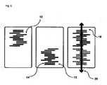
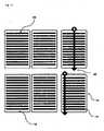
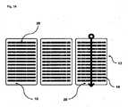
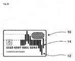
本発明では、カード状物体は、本発明の特に好ましい実施例では、カード、たとえばクレジット・カードの形態を持つ3次元の製品であることが好ましい。当業者は、カードが好ましくは平坦であるように構成されること、すなわち、好ましい物体の長さ又は幅よりも大幅に低い高さを持つことを理解されよう。具体的には、カード状物体は、平面状に形づくることができ、すなわち、低い高さに対して大きなベース領域を備えることができ、ここで本発明によれば、ベース領域を備えるカード状物体が表面センサ上に置かれる場合、それにより物体と表面センサとの相互作用のための大きな有効表面を有利に作成することは、特に好ましい。さらなる実施例において、カード形状の物体は、物体の幅よりも大幅に長い、長さを持つことが好ましい。たとえば、典型的なクレジット・カードでは、長さは86mm、幅は54mmであり、これは約1.6の比率に一致する。本発明では、従来のクレジット・カードは、長さが物体の幅よりも大幅に長いカード形状の物体の一実例である。たとえば、カード形状の物体が、長さと幅との比率が1.5より大きい物体を意味する場合がある。しかし本発明では、カード形状の物体が、好ましくは物体の長さと幅との間の比率が1であることを特徴とする、正方形のベース領域を備えることもまた好ましい場合がある。ある実施例では、カード形状の物体は、たとえばロール上に設けることができる織物形状の材料であることが好ましい。カード状物体は、表面センサを損傷又は破壊することなく、表面センサ上に置くことができるよう構成されることが特に好ましい。カード状物体は、たとえば、紙、厚紙、プラスチック、織物を含むがそれに限定されるものではない群から選択することができる材料を含むことが好ましい。 According to the invention, the card-like object is preferably a three-dimensional product in the form of a card, eg a credit card, in a particularly preferred embodiment of the invention. Those skilled in the art will appreciate that the card is preferably configured to be flat, ie having a height significantly less than the length or width of the preferred object. In particular, the card-like object can be shaped planar, i.e. with a large base area for a low height, where according to the invention the card-like object with the base area is placed on the surface sensor, thereby advantageously creating a large effective surface for interaction of the object with the surface sensor. In a further embodiment, the card-shaped object preferably has a length that is significantly greater than the width of the object. For example, a typical credit card is 86 mm long and 54 mm wide, which corresponds to a ratio of about 1.6. For purposes of the present invention, a conventional credit card is an example of a card-shaped object whose length is significantly greater than its width. For example, a card-shaped object may mean an object with a length to width ratio greater than 1.5. However, it may also be preferred according to the invention that the card-shaped object comprises a square base area, preferably characterized by a ratio of 1 between the length and the width of the object. In one embodiment, the card-shaped object is preferably a woven-shaped material that can be provided, for example, on a roll. It is particularly preferred that the card-like object is configured so that it can be placed on the surface sensor without damaging or destroying the surface sensor. The card-like object preferably comprises a material that can be selected from the group including, but not limited to, paper, cardboard, plastic, fabric.
本発明では、時間依存信号は、好ましくは時間で変化する信号、すなわち単独で、又は外部の影響によって時間の経過と共に変化する信号を表すことが好ましい。本発明に関しては、時間依存信号は、カード状物体上の個々の要素の配置によって確立され、入力手段とカード状物体との間の相対的な動きによって生成される。本発明では、導電性構造体は、少なくとも2つの個々の要素を備えることが好ましい。しかし、本発明のある適用例では、本発明のために、導電性構造体が、より多数の個々の要素を備えることが好ましい場合がある。本発明では、様々な用途のために、カード状物体が複数の導電性構造体を備えることもまた好ましい場合がある。こうした構造体は、たとえば、物体上に互いに平行に配置することができ、又は互いに対してある角度をなすように回転して配置することができ、それによって、個々の導電性構造体間に複雑な相互作用の可能性が生じ得る。 In the present invention, a time-dependent signal preferably denotes a time-varying signal, ie a signal that changes over time either alone or due to external influences. With respect to the present invention, the time-dependent signal is established by the placement of individual elements on the card-like object and produced by relative movements between the input means and the card-like object. According to the invention, the electrically conductive structure preferably comprises at least two individual elements. However, in some applications of the present invention it may be preferred for the present invention that the electrically conductive structure comprises a greater number of individual elements. According to the invention, it may also be preferred for the card-like object to comprise a plurality of electrically conductive structures for various applications. Such structures may, for example, be arranged parallel to each other on the object, or may be arranged rotated at an angle to each other, thereby creating a complex structure between the individual conductive structures. interactions can occur.
本発明では、導電性構造体を形成する個々の要素は、互いに類似している、すなわち、たとえば、異なる長さ及び/又は幅を持つストリップからなり、それらは横並びに配置され得る、そしてたとえばストリップ間で同じ間隔又は異なる間隔を持つことができることが、好ましい場合がある。かかる個々の要素は、好ましくは、その長さが異なる場合があっても、すべての個々の要素が線状であるという点で、互いに類似している。しかし、導電性構造体の個々の要素が互いに類似していないこと、すなわち、相異なる形状を持っていることが好ましい場合もある。 According to the invention, the individual elements forming the electrically conductive structure are similar to each other, i.e. consist, for example, of strips having different lengths and/or widths, which can be arranged side by side, and for example strips It may be preferable to be able to have the same or different spacings between. Such individual elements are preferably similar to each other in that all individual elements are linear even though their lengths may vary. However, it may be preferred that the individual elements of the electrically conductive structure are dissimilar to each other, ie have different shapes.
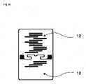
本発明のさらに好ましい構成では、導電性構造体の個々の要素は、互いに電気的に分離されている。導電性構造体の個々の要素の、互いからの好ましい空間的及び/又は電気的分離は、たとえば、それぞれの場合、2つの個々の要素が互いから間隔を空けて配置されることで実現させることができ、ここで導電性構造体内の個々の要素間の前記間隔は、同じであっても相異なっていてもよい。本発明では、導電性構造体は、互いに電気的に分離された少なくとも2つの個々の要素を備え、ここで個々の要素は、1つの平面内に配置されることが特に好ましい。本発明では、「1つの平面内」という用語は、好ましくは、導電性構造体が、たとえば、好ましくは平面状に形づくられるカード状物体の表及び/又は裏に配置されることを意味する。 In a further preferred configuration of the invention, the individual elements of the electrically conductive structure are electrically isolated from each other. A preferred spatial and/or electrical isolation of the individual elements of the electrically conductive structure from one another is achieved, for example, in each case by two individual elements being spaced apart from each other. where the spacing between individual elements within the conductive structure may be the same or different. According to the invention, the electrically conductive structure comprises at least two individual elements electrically separated from each other, wherein the individual elements are particularly preferably arranged in one plane. In the present invention, the term "in one plane" preferably means that the electrically conductive structures are arranged, for example, on the front and/or the back of a card-like object, which is preferably shaped like a plane.
本発明では、「静電容量式表面センサ」という用語は、好ましくは、外部の衝撃又は影響、たとえばタッチ・スクリーン領域の接触を感知し、それを関連する論理回路を用いて評価することができるタッチ・スクリーンを備える、かかるデバイスを表す。かかる表面センサは、たとえば、機械をより簡単に操作するために使用される。好ましくはタッチ・スクリーン又は表面センサとも呼ばれる静電容量式スクリーンへの入力を行うために、指に加えて、特別なスタイラス又は同様のデバイスを使用することができる。本発明では、指及び特別なスタイラスは、好ましくは入力手段と呼ばれる。これらの入力手段は、好ましくは、表面センサ内の行電極と列電極との間の静電容量結合を変化させることができる。本発明では、好ましくは入力手段とカード状物体との間の相対的な動きによって時間依存信号を生成するよう適合される、かかる入力手段は、先行技術では説明されていない。静電容量式の、好ましくは、タッチ感応型のスクリーンは、入力手段の位置を検出するよう適合されることが好ましい。 In the present invention, the term "capacitive surface sensor" preferably senses external shocks or influences, such as touch on the touch screen area, which can be evaluated using associated logic circuitry. It represents such a device with a touch screen. Such surface sensors are used, for example, to operate machines more easily. In addition to a finger, a special stylus or similar device can be used to provide input to the capacitive screen, preferably also called a touch screen or surface sensor. In the present invention, fingers and special styluses are preferably referred to as input means. These input means are preferably capable of varying the capacitive coupling between row and column electrodes within the surface sensor. In the present invention such input means, which are preferably adapted to generate a time dependent signal by relative movement between the input means and the card-like object, are not described in the prior art. The capacitive, preferably touch-sensitive screen is preferably adapted to detect the position of the input means.
表面センサは、典型例では、スマートフォン、携帯電話、ディスプレイ、タブレットPC、タブレット・ノートブック、タッチパッド・デバイス、グラフィック・タブレット、テレビ、PDA、MP3プレーヤ、トラックパッド、及び/又は静電容量式入力デバイスであり得るがそれに限定されるものではない、電気式デバイス内に備えられる。タッチ・スクリーンは、好ましくは、タッチ感応型スクリーン、表面センサ、又はセンサ・スクリーンとも呼ばれる。表面センサは、必ずしもディスプレイ又はタッチ・スクリーンと組み合わせて使用する必要はない。本発明では、表面センサは、デバイス、物体、及び/又は装置内に見えるように、又は見えないように一体化されることが好ましい場合もある。 Surface sensors are typically found in smartphones, mobile phones, displays, tablet PCs, tablet notebooks, touchpad devices, graphics tablets, televisions, PDAs, MP3 players, trackpads, and/or capacitive inputs. It is provided within an electrical device, which can be, but is not limited to, a device. The touch screen is preferably also called touch-sensitive screen, surface sensor or sensor screen. A surface sensor need not necessarily be used in combination with a display or touch screen. In the present invention, it may be preferred that the surface sensor is visibly or invisibly integrated within the device, object and/or apparatus.
本発明では、たとえば、マルチタッチ対応の表面センサを使用することが好ましい場合がある。かかる表面センサは、好ましくは、複数のタッチを同時に識別するよう適合され、たとえば、タッチ・スクリーン上に表示される要素を回転又は拡大縮小できるようにする。 In the present invention, it may be preferable to use, for example, multi-touch capable surface sensors. Such surface sensors are preferably adapted to identify multiple touches simultaneously, allowing for example to rotate or scale elements displayed on the touch screen.
本発明では、たとえば、マルチタッチ対応ではない表面センサを使用することが好ましい場合もある。特にたとえばスマートフォンなどの、より旧型のデバイスでは、一度に1つのタッチしか識別することができない。表面センサ上の複数のタッチ・ポイントの静止画像を生成する情報キャリアは、先行技術で知られる。かかる情報キャリアは、その表面センサがマルチタッチ対応ではない、より旧型のデバイスとは互換性がない。カード状物体を用いて静電容量式表面センサ上で時間依存信号を生成する、本発明による方法が、こうしたいわゆるシングルタッチ対応の表面センサと互換性があることは、まったく驚くべきことであった。提案される方法がこうしたシングルタッチ対応の表面センサと互換性があるという表現は、好ましくは本発明では、かかる表面センサがこの方法を実行するために、又は提案された方法をこうしたデバイス上で「実行」するように、使用され得ることを意味する。 In the present invention, it may be preferable to use, for example, surface sensors that are not multi-touch capable. Especially older devices, such as smartphones, can only identify one touch at a time. Information carriers that generate still images of multiple touch points on a surface sensor are known in the prior art. Such information carriers are not compatible with older devices whose surface sensors are not multi-touch capable. It was quite surprising that the method according to the invention for generating a time-dependent signal on a capacitive surface sensor using a card-like object is compatible with such so-called single-touch capable surface sensors. . A statement that the proposed method is compatible with such single-touch-enabled surface sensors means that the present invention preferably allows such surface sensors to perform the method or implement the proposed method on such devices as " It means that it can be used to "perform".
具体的には、表面センサは、電極の構造体に接続することができる、好ましくはタッチ・コントローラと呼ばれる、少なくとも1つの能動回路を備える。表面センサは、先行技術において知られており、その電極は、たとえば、機能が互いに相異なる電極群を含む。たとえば、こうした電極は、送信電極及び受信電極であってもよく、特に好ましい配置では、列及び行の形態で配置され得る、すなわち、具体的には、少なくとも1つの送信電極及び1つの受信電極が互いに交差する、又は重なるノード・ポイントを形成し得る。好ましくは、ノードの領域における交差する送信及び受信電極は、本質的に90°の角度をなすように、互いに整列される。本発明では、表面センサの送信電極と受信電極との間に静電場が形成されることが特に好ましく、静電場は、たとえば、表面センサの表面を導電性デバイスと接触させることによる、又は表面センサの表面の接地、すなわち電荷の放電による、変化の影響を受けやすい。 Specifically, the surface sensor comprises at least one active circuit, preferably called a touch controller, which can be connected to the structure of electrodes. Surface sensors are known in the prior art, the electrodes of which, for example, comprise groups of electrodes differing from one another in function. For example, such electrodes may be transmitter electrodes and receiver electrodes, and in a particularly preferred arrangement may be arranged in columns and rows, i.e. in particular at least one transmitter electrode and one receiver electrode. Node points may be formed that intersect or overlap each other. Preferably, the crossing transmit and receive electrodes in the region of the node are aligned with each other so as to form an angle of essentially 90°. In the present invention it is particularly preferred that an electrostatic field is formed between the transmitting and receiving electrodes of the surface sensor, for example by bringing the surface of the surface sensor into contact with an electrically conductive device or by surface ground, i.e., subject to change due to discharge of charge.
本発明では、タッチ・コントローラは、好ましくは、それぞれの場合において、1つ又は複数の送信電極と1つ又は複数の受信電極との間で信号が送信されるように、電極を制御することが好ましく、この信号は、好ましくは電気信号、たとえば、電圧、電流、又は電位(差)であり得る。静電容量式表面センサ内のこうした電気信号は、好ましくは、タッチ・コントローラによって評価され、デバイスのオペレーティング・システム向けに処理される。タッチ・コントローラによってオペレーティング・システムに送信される情報は、いわゆる個々の「タッチ」を表し、それぞれ単一の識別されたタッチと考えられ得る。こうしたタッチは、好ましくは、パラメータであるタッチのx座標、タッチのy座標、タッチのタイム・スタンプ、及びタッチの種類によって特徴づけられる。パラメータであるx座標及びy座標は、タッチ・スクリーン上の入力の位置を表す。各座標ペアは、好ましくは、対応する場所で入力がいつ行われたかを表すタイム・スタンプに関連づけられる。当業者は、以下の種類のタッチ信号が存在することを知っている。タッチ開始、タッチ移動、タッチ終了、及びタッチ取消。「タッチ開始」という用語は、好ましくは、ユーザによるタッチ入力の開始を表す。「タッチ開始」は、たとえばユーザのタッチによって行われ得る。「タッチ移動」という用語は、好ましくは、たとえばタッチ・スクリーンから指を上げることのない、タッチ・スクリーン上の入力の動きを表す。「タッチ終了」という用語は、好ましくは、タッチ入力の終了を表し、これは、たとえば、ユーザがタッチ・スクリーンから指を上げることによって行われ得る。「タッチ取消」という用語は、好ましくは、タッチ・コントローラによってタッチ入力が中止される状態を表す。「タッチ取消」は、たとえば、同時に多すぎるタッチ入力が検出された場合に必要であり得る。本発明では、時間依存信号は、好ましくは、かかるタッチ又はタッチ入力の量を含む。言い換えれば本発明では、好ましくは、時間依存信号は、タッチ及び/又はタッチ入力の量によって形成される。本発明に関しては、時間依存信号である表面センサ内のこうした信号は、カード状物体上の個々の要素の配置によって確立することができる。 In the present invention, the touch controller is preferably capable of controlling the electrodes such that in each case signals are transmitted between one or more transmitting electrodes and one or more receiving electrodes. Preferably, this signal may preferably be an electrical signal, eg voltage, current or potential (difference). Such electrical signals in the capacitive surface sensor are preferably evaluated by the touch controller and processed for the device's operating system. The information sent by the touch controller to the operating system represents so-called individual "touches", each of which can be thought of as a single identified touch. Such touches are preferably characterized by the parameters x-coordinate of touch, y-coordinate of touch, time stamp of touch, and type of touch. The parameters x and y coordinates represent the position of the input on the touch screen. Each coordinate pair is preferably associated with a time stamp representing when the input was made at the corresponding location. Those skilled in the art know that the following types of touch signals exist. Start Touch, Move Touch, End Touch, and Cancel Touch. The term "touch initiation" preferably refers to the initiation of touch input by a user. A "touch initiation" may be performed by a user's touch, for example. The term "touch movement" preferably describes movement of an input on a touch screen, for example without lifting a finger from the touch screen. The term "touch termination" preferably denotes termination of touch input, which may be done, for example, by the user lifting a finger from the touch screen. The term "touch canceled" preferably describes a condition in which touch input is canceled by the touch controller. "Touch cancellation" may be necessary, for example, when too many simultaneous touch inputs are detected. In the present invention, the time dependent signal preferably includes the amount of such touches or touch inputs. In other words, according to the invention, the time-dependent signal is preferably formed by the amount of touch and/or touch input. With respect to the present invention, such signals in the surface sensor, which are time dependent signals, can be established by the arrangement of individual elements on the card-like object.
本発明では、入力手段とカード状物体との間の相対的な動きによって表面センサ上に生成される時間依存信号は、カード状物体上の個々の要素の配置によって変わり、具体的には、直接的である、すなわち、好ましくはカード状物体を使用しない表面センサ上の入力手段の入力と異なることが好ましい。具体的には、2つの状況が区別される。一方は、入力手段を備えた表面センサ上の直接の動的な入力であり、他方は、入力手段と表面センサとの間にカード状物体が介在する動的な入力である。本発明では、表面センサ上に入力手段を備えた直接入力を、基準入力として指定することが好ましい。本発明では、カード状物体上の個々の要素の配置が、直接の動的な入力に変化を引き起こし、その結果、時間依存信号が表面センサ上に生成されることが好ましい。本発明の好ましい実施例では、静電容量式表面センサ上の相対的な動きから得られる時間依存信号が、好ましくはカード状物体を使用することなしに生じる入力手段を用いた基準入力に対して変化するような、サイズ、間隔、及び形状に対する導電性構造体の個々の要素を形成することを提供する。本発明では、この変換プロセスは、好ましくは、変調、確立、変更、歪み、又はシフトと呼ばれる。 In the present invention, the time-dependent signal generated on the surface sensor by the relative movement between the input means and the card-like object depends on the arrangement of the individual elements on the card-like object, in particular the direct ie different from the input of the input means on the surface sensor, which preferably does not use a card-like object. Specifically, two situations are distinguished. One is direct dynamic input on a surface sensor with input means and the other is dynamic input with a card-like object interposed between the input means and surface sensor. In the present invention, a direct input with input means on the surface sensor is preferably designated as the reference input. In the present invention it is preferred that the placement of individual elements on the card-like object causes a change in the direct dynamic input, resulting in a time dependent signal being generated on the surface sensor. In a preferred embodiment of the invention, the time dependent signal resulting from relative movement on the capacitive surface sensor is compared to a reference input using input means which preferably occurs without using a card-like object. It provides for forming the individual elements of the conductive structure to varying sizes, spacings and shapes. In the present invention, this transformation process is preferably called modulation, establishment, alteration, distortion or shifting.
本発明の好ましい構成では、静電容量式表面センサ上に結果として得られる時間依存信号は、位置、速度、方向、形状、信号の中断、周波数、及び/又は信号強度に関して、カード状物体を使用することなく行われる入力手段を用いた基準入力によって確立される基準信号に対して少なくとも部分的に変化する。本発明では、それは好ましくは、提案された方法によって生成され得る、結果として得られる時間依存信号であることが好ましい。導電性構造体の個々の要素上の直線的な線状の動きの形での例示的な入力から始まり、これは、本発明では好ましくは、生成された時間依存信号が、カード状物体、又はその導電性構造体による変調のために、入力手段の直線的な線状の入力に対して異なる位置、方向、形状、及び/又は信号強度を持ち得ること、すなわちたとえば、空間的にずれ、歪み、且つ/又はシフトされ、直線的な線状の動きとは異なる形状を持ち、異なる方向を指し示し、又は予期しない信号強度を持つ時間依存信号が、表面センサによって識別されることを意味する。 In preferred configurations of the invention, the resulting time-dependent signal on the capacitive surface sensor uses a card-like object with respect to position, velocity, direction, shape, signal interruption, frequency, and/or signal strength. at least partially with respect to a reference signal established by a reference input using the input means performed without. In the present invention it is preferably the resulting time dependent signal that can be generated by the proposed method. Starting with an exemplary input in the form of linear linear movements on individual elements of the electrically conductive structure, which in the present invention preferably produces a time-dependent signal, which is a card-like object, or Due to the modulation by its conductive structure, it may have a different position, orientation, shape and/or signal strength for a straight linear input of the input means, i.e. spatially offset, distorted and/or time-dependent signals that are shifted, have a different shape than straight linear motion, point in a different direction, or have an unexpected signal strength are identified by the surface sensor.
たとえば、本発明のための入力手段の適用される実例として、ユーザが指で静電容量式表面センサ上を掃引する場合、表面センサは、実際に指、すなわち入力手段によってタッチされた表面センサのスクリーン上の位置で、この動きを本質的に検出する。指の直線的な線状の動きは、好ましくは、本質的に直線的な線状の動きとして、表面センサによって検出される。カード状物体が存在しない、かかる入力は、好ましくは、本発明では基準入力と呼ばれる。 For example, as an applied illustration of the input means for the present invention, if a user sweeps a finger over a capacitive surface sensor, the surface sensor is actually the surface sensor touched by the finger, i.e. the input means. Positions on the screen essentially detect this movement. Linear linear motion of the finger is preferably detected by the surface sensor as essentially linear linear motion. Such inputs, in which no card-like object is present, are preferably called reference inputs in the present invention.
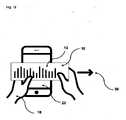
本発明に関しては、好ましくは、カード状物体が入力手段と表面センサとの間に配置され、具体的には、カード状物体が表面センサ上に置かれ得ることが提供される。カード状物体は、好ましくは導電性の個々の要素を具備する導電性構造体を備える。本発明の可能な適用される実例では、カード状物体又は表面センサのユーザが、カード状物体上、特に導電性構造体上で指を動かすことが提供される。これによってカード状物体は、好ましくは、表面センサ上に載っており、その結果ユーザがタッチする導電性構造体の個々の要素は、ユーザの指の動きによって起動されることにより、表面センサに「見える」ようになる。本発明者らは、導電性構造体を備えるカード状物体を使用することにより、表面センサ上の入力を基準入力と比較して変更できることを認識した。この変更は、本発明では、好ましくは、変調と呼ばれる。好ましくは、導電性構造体の個々の要素が、入力手段との接触によって起動し、それによって表面センサが接触を検出でき、その結果得られる時間依存信号は、カード状物体上の個々の要素の配置によって、たとえば基準入力と比較して空間的に歪められることが生じる。たとえば、導電性構造体を持たないカード状物体上で仮想直線に沿って入力手段が実行される場合、表面センサは、入力手段の直線的な動きを基準入力として検出するであろう。しかし、カード状物体が入力手段と表面センサとの間に配置され、その上に導電性構造体の個々の要素が、たとえばカード状物体の左側に配置される場合、表面センサは、入力手段がカード状物体上を移動するとき、左にシフトした、すなわち基準入力と比較して歪んだ、結果として生じる信号を検出するであろう。本発明に関して、生成された時間依存信号は、好ましくは、入力手段とカード状物体との間の相対的な動きの、導電性構造体による偏向、歪み、及び/又はシフト後の検出に一致する。相対的な動きは動きs(t)があるので時間に依存し、従って検出された信号もまた、好ましくは時間の関数を表すので、時間に依存する。本発明では、これは、好ましくは、時間依存信号がカード状物体上の入力手段の時間シーケンスに対応することを意味し、ここで特にタッチのx座標及びy座標によって特徴づけられる、結果として得られた時間依存信号の検出された位置は、カード状物体なしで生成された基準信号と比較して、導電性構造体によって偏向され、歪み、且つ/又はシフトされ得る。本発明では、この歪み、偏向、及び/又はシフトは、好ましくは、時間依存信号の位置の変化と呼ばれる。 With respect to the invention it is preferably provided that the card-like object is arranged between the input means and the surface sensor, in particular that the card-like object can be placed on the surface sensor. The card-like object preferably comprises an electrically conductive structure comprising electrically conductive individual elements. In a possible application of the invention it is provided that the user of the card-like object or surface sensor moves his finger on the card-like object, in particular on the conductive structure. The card-like object thereby preferably rests on the surface sensor, so that individual elements of the conductive structure touched by the user are activated by movement of the user's finger, thereby causing the surface sensor to " It becomes visible. The inventors have recognized that by using a card-like object with conductive structures, the input on the surface sensor can be altered compared to a reference input. This modification is preferably called modulation in the present invention. Preferably, individual elements of the electrically conductive structure are activated by contact with the input means, such that the contact can be detected by the surface sensor, and the resulting time-dependent signal is associated with individual elements on the card-like object. The placement results in spatial distortion compared to, for example, a reference input. For example, if the input means is performed along an imaginary straight line on a card-like object without conductive structures, the surface sensor will detect the linear movement of the input means as a reference input. However, if the card-like object is arranged between the input means and the surface sensor, and the individual elements of the conductive structure on it are arranged, for example, on the left side of the card-like object, the surface sensor detects that the input means As it moves over the card-like object, it will detect the resulting signal shifted to the left, ie distorted compared to the reference input. With respect to the present invention, the generated time-dependent signal preferably corresponds to the detection of the relative movement between the input means and the card-like object after deflection, distortion and/or shifting by the electrically conductive structure. . The relative motion is time dependent as is the motion s(t) and thus the detected signal is also time dependent as it preferably represents a function of time. In the present invention, this preferably means that the time-dependent signal corresponds to the time sequence of the input means on the card-like object, where in particular the resulting x- and y-coordinates of the touch are characterized. The detected position of the time-dependent signal generated may be deflected, distorted and/or shifted by the conductive structure compared to a reference signal generated without the card-like object. In the present invention this distortion, deflection and/or shift is preferably referred to as a change in position of the time dependent signal.
本発明では、速度に差が生じること、すなわち、たとえば、入力手段の急速な動きが遅い時間依存信号に変調されることが好ましい場合もある。時間依存信号が、特定の速度プロファイルを持っていることが好ましい場合もある。たとえば、導電性構造体を備えないカード状物体上で仮想直線に沿って入力手段が実行される場合、表面センサは、直線を表し、ほぼ一定の速度を持つ時間依存信号を、基準入力として検出するであろう。しかし、カード状物体が入力手段と表面センサとの間に配置され、その上に導電性構造体の個々の要素が、たとえばカード状物体上に特定の間隔で配置された場合、表面センサは、入力手段がカード状物体上を移動するとき、基準入力に対して特定の速度プロファイルを持つ、結果として生じる信号を検出するであろう。この場合、入力手段がカード状物体を横切って移動するとき、入力手段は徐々に、カード状物体上の導電性要素と動作可能に接触するようになる。すなわち、入力手段は、徐々に導電性要素をカバーする。入力手段が導電性の個々の要素に到達すると、結果として生じる信号の位置は、好ましくは、この時点で個々の要素の方向にシフトされる。 In the present invention it may be preferred that the speed is differential, ie for example a rapid movement of the input means is modulated into a slow time dependent signal. It may be desirable for the time dependent signal to have a specific velocity profile. For example, if the input means is performed along a virtual straight line on a card-like object without conductive structures, the surface sensor detects as a reference input a time-dependent signal representing the straight line and having a substantially constant velocity. would do. However, if a card-like object is placed between the input means and the surface sensor, on which the individual elements of the conductive structure are placed, for example on the card-like object at certain intervals, the surface sensor As the input means moves over the card-like object, it will detect a resulting signal with a specific velocity profile relative to the reference input. In this case, as the input means moves across the card-like object, the input means gradually come into operative contact with the conductive elements on the card-like object. That is, the input means gradually cover the conductive elements. When the input means reaches a conductive individual element, the position of the resulting signal is preferably shifted towards the individual element at this point.
具体的な実例では、入力手段は、カード状物体上で、仮想直線に沿ってy方向に一定の速度で移動する。入力手段が導電性要素と接触しない限り、結果として得られた時間依存信号は、本質的にタイム・スタンプ及びそれぞれのy座標が異なるタッチによって本質的に特徴づけられ、動きの速度は本質的に一定である。入力手段が導電性の個々の要素に到達すると、この時点で、好ましくは、結果として得られる信号の位置が個々の要素の方向にシフトされる。すなわち、単一のタッチは、前のタッチと比較して、y座標に関してはるかに大きくシフトされる。結果として得られた時間依存信号の個々のタッチのパラメータを使用して、速度プロファイルを計算することができる。本発明では、特に入力手段が導電性の個々の要素と接触したときに、速度プロファイルの変動を識別することができることが好ましい。 In a concrete example, the input means moves at a constant speed in the y-direction along an imaginary straight line on the card-like object. As long as the input means is not in contact with the conductive element, the resulting time-dependent signal is essentially characterized by touches with different time stamps and respective y-coordinates, and the speed of movement is essentially constant. When the input means reaches a conductive individual element, at this point the position of the resulting signal is preferably shifted in the direction of the individual element. That is, a single touch is shifted much more with respect to the y-coordinate compared to the previous touch. The individual touch parameters of the resulting time-dependent signal can be used to calculate velocity profiles. It is preferred in the present invention to be able to identify variations in the velocity profile, especially when the input means is in contact with an electrically conductive individual element.
本発明では、たとえば、カード状物体の導電性構造体上で連続的な動きが起こる場合、信号が中断されることが好ましい場合もある。この場合導電性構造体は、好ましくは、意図的に間隙を持ち、その結果表面センサで検出される時間依存信号は、中断及び/又は一時停止する。すなわち、たとえば、それはもはや連続ではなく、且つ/又は、たとえば「ジャンプ」している。さらに、生成された時間依存信号は、カード状物体上の導電性構造体の構成により、中断があることが好ましい場合がある。定期的に繰り返される信号部分のシーケンスが生成され、これらが一体になって、周波数に関連づけることが可能な時間依存信号を形成することが好ましい場合もある。 In the present invention it may be preferred, for example, that the signal is interrupted when continuous movement occurs on the conductive structure of the card-like object. In this case the conductive structure is preferably intentionally gapped so that the time-dependent signal detected by the surface sensor is interrupted and/or paused. That is, for example, it is no longer continuous and/or "jumps", for example. Furthermore, the generated time-dependent signal may preferably have interruptions due to the configuration of the conductive structures on the card-like object. It may be preferred to generate a sequence of periodically repeating signal portions which together form a time dependent signal that can be related to frequency.
本発明では、カード状物体上の入力は、入力手段を用いて行われることが好ましい。カード状物体上の入力手段の動きは、たとえば、線の形の直線的な動きであり得る。かかる線状の動きは、タッチ感応型ディスプレイ上で直接実行される場合、表面センサによって線状の入力として識別される。しかし、導電性構造体を備える本発明によるカード状物体上で線状の動きが実行される場合、表面センサは、カード状物体の導電性構造体の空間的構成によって変わるスナップショットを「見る」。すなわち、偶然にも導電性構造体のすべての要素が、もっぱら対称的に及び/又は互いに正確に合致して配置されていない限り、スナップショットは通常、もはや線状ではないであろう。従って、物体上の入力手段の実際の動きと、この動きの静電容量式表面センサの認識は異なり、導電性構造体の構成要素及び/又は要素の空間的配置によってもたらされているカード状物体のこの変換は、本発明では好ましくは、変調、確立、変化、歪み、又はシフトと呼ばれる。本発明では、カード状物体上の入力手段の動きは、入力と呼ばれ、表面センサの認識、すなわち、表面センサが物体によって変調された入力から識別するものは、時間依存信号と呼ばれることが好ましい。 In the present invention, the input on the card-like object is preferably performed using input means. The movement of the input means on the card-like object can be linear movement, for example in the form of lines. Such linear movements, when performed directly on the touch-sensitive display, are identified as linear inputs by the surface sensor. However, if a linear movement is performed on a card-like object according to the invention comprising conductive structures, the surface sensor "sees" a snapshot that varies with the spatial configuration of the conductive structures of the card-like object. . That is, unless by chance all the elements of the conductive structure are arranged exclusively symmetrically and/or in exact alignment with each other, the snapshot will generally no longer be linear. Therefore, the actual movement of the input means on the object and the capacitive surface sensor's perception of this movement are different, the card-like effect being effected by the spatial arrangement of the components and/or elements of the electrically conductive structure. This transformation of the object is preferably called modulation, establishment, change, distortion or shift in the present invention. In the present invention, the movement of the input means on the card-like object is called input and the recognition of the surface sensor, i.e. what the surface sensor distinguishes from the input modulated by the object, is preferably called time dependent signal. .
静電容量式表面センサ上での時間依存信号の生成は、好ましくは、カード状物体によって入力を時間依存信号に変換することにより実行され、時間依存信号は、好ましくは、静電容量式表面センサ内で生成される。本発明では、この表現は、好ましくは、時間依存信号が入力手段とカード状物体との間の相対的な動きによって生成されることを意味し、時間で変化する信号は、好ましくは、表面センサによって検出される。本発明では、入力は、カード状物体上で行われ、識別は、表面センサ上で行われるので、これは好ましくは、信号の送信と呼ばれる。 The generation of the time dependent signal on the capacitive surface sensor is preferably performed by converting the input into a time dependent signal by means of a card-like object, the time dependent signal preferably being generated by the capacitive surface sensor generated within. In the present invention, this expression preferably means that the time-dependent signal is generated by the relative movement between the input means and the card-like object, the time-varying signal preferably being generated by a surface sensor detected by Since in the present invention the input is made on the card-like object and the identification is made on the surface sensor, this is preferably called sending the signal.
導電性構造体は、非常に柔軟に構成することができ、さらに、入力手段の様々な動きは、カード状物体上の動きの様々な可能性を列挙することによって考えられるので、カード状物体を用いて、非常に高いデータ密度を取得可能な方法を提供することができる。本発明による導電性構造体を備えるデバイスが、たとえば、好ましくは少なくとも12ビット、特に好ましくは少なくとも16ビットのデータ容量を持つことができることは、まったく驚くべきことであった。このデータ容量が、好ましくは小さな表面上で実現でき、従って高いデータ密度をもたらすことは、まったく驚くべきことであった。さらに、この方法は、使用されるとき、カード状物体が表面センサ上に簡単に置かれるので、特にユーザ・フレンドリである。従来のデータ・キャリア並びに表面センサとデータ・キャリアとの間の信号伝送方法の場合のように、カード状物体の特定の領域が、表面センサの特定の領域上に載るか載らないかを確認する必要はもはやない。 The conductive structure can be configured very flexibly, and various movements of the input means can be considered by enumerating various possibilities of movements on the card-like object. can be used to provide a method capable of obtaining very high data densities. It was quite surprising that a device comprising an electrically conductive structure according to the invention can, for example, preferably have a data capacity of at least 12 bits, particularly preferably at least 16 bits. It was quite surprising that this data capacity can be realized on a preferably small surface, thus resulting in high data density. Moreover, this method is particularly user-friendly when used, since the card-like object is simply placed on the surface sensor. As with conventional data carriers and signal transmission methods between the surface sensor and the data carrier, it is checked whether a specific area of the card-like object rests on or does not rest on a specific area of the surface sensor. no longer needed.
カード形状の物体上の入力手段の動きの様々な可能性を列挙することにより、ユーザと静電容量式データ・キャリアとのまったく新しい相互作用の可能性が開かれる。本発明の好ましい実施例では、複数の独立した導電性構造体が、カード状物体上に配置される。1つの例示的な実施例では、2つの導電性構造体が配置され、それぞれが導電性構造体自体の動作トラックを備え、この実施例では、垂直に1回及び水平に1回実行する。これは、上から下、下から上、左から右、及び右から左の合計4方向の相互作用という結果をもたらす。各導電性構造体は、相対的な動きの方向の関数として、静電容量式表面センサを含むデバイス上での、様々な作用をトリガすることができる。同じカード形状の物体を使って、複数の様々な作用をトリガできることは、まったく驚くべきことであった。これは、先行技術に対する重要な利点を示している。先行技術から知られているバーコード、2Dバーコード、無線タグ、並びに静電容量式データ・キャリアの両方において、その適用例は、本質的に物体の識別に限定されている。驚くべきことに、本発明により、相互作用のさらなる機会が開かれる。 The enumeration of different possibilities of movement of the input means on the card-shaped object opens up completely new possibilities of interaction between the user and the capacitive data carrier. In a preferred embodiment of the invention, a plurality of independent conductive structures are arranged on the card-like object. In one exemplary embodiment, two conductive structures are arranged, each with its own track of motion, in this example running once vertically and once horizontally. This results in interactions in a total of four directions: top-to-bottom, bottom-to-top, left-to-right, and right-to-left. Each conductive structure can trigger different actions on devices including capacitive surface sensors as a function of relative direction of motion. It was quite surprising that the same card-shaped object could be used to trigger multiple different effects. This represents a significant advantage over the prior art. In both barcodes, 2D barcodes, radio tags and capacitive data carriers known from the prior art, their application is essentially limited to the identification of objects. Surprisingly, the present invention opens up additional opportunities for interaction.
本発明に関しては、時間依存信号の生成は、入力手段とカード状物体との間の相対的な動きによって行われる。本発明では、これは、好ましくは、入力手段がカード状物体に対して移動する、若しくはカード状物体が入力手段に対して移動すること、又は入力手段と物体との両方が移動することを意味し、両方の移動は、本発明ではまさに相対的な動きではなく、平行の動きをもたらすことになるため、同じ方向及び同じ速度ではないことが好ましい。本発明では、相対的な動きの位置、方向及び/又は速度が、時間依存信号の生成に影響し、特にどのように時間依存信号を空間的に形成するかを決定することが、特に好ましい。この決定は、特に、相対的な動きで生じる入力が、時間依存信号に変換され、及び/又は変調されることを用いて、導電性構造体の幾何形状と協働して行われる。 As regards the invention, the generation of the time-dependent signal is effected by the relative movement between the input means and the card-like object. In the present invention this preferably means that the input means moves relative to the card-like object, or the card-like object moves relative to the input means, or both the input means and the object move. However, it is preferred that both movements are not in the same direction and at the same speed, as in the present invention both movements will result in parallel rather than just relative movement. In the present invention it is particularly preferred that the position, direction and/or speed of the relative movement influence the generation of the time dependent signal and in particular determine how the time dependent signal is spatially shaped. This determination is made in cooperation with the geometry of the conductive structure, in particular by means of which the relative motion-generated input is converted and/or modulated into a time-dependent signal.
本発明では、入力手段とカード状物体との間の相対的な動きは、好ましくは、第2の接点と呼ばれ、本発明に関しては、常に動的に構成されることが好ましい。 In the present invention the relative movement between the input means and the card-like object is preferably referred to as the second contact point and is always dynamically configured in the context of the present invention.
第2の態様では、本発明は、以下のステップを含む、カード状物体を識別する方法に関する。
a.複数の個々の要素を具備する導電性構造体を備える、カード状物体を提供するステップ。
b.静電容量式表面センサ上にカード状物体を置くステップであって、それによって第1の接点が形成されるステップ。
c.入力手段とカード状物体との間の相対的な動きを実行するステップであって、それによって第2の接点を形成するステップ。
d.相対的な動きの関数としての、時間依存信号を生成するステップ。
e.カード状物体を識別するために、表面センサを備えるデバイスによって、静電容量式表面センサ上の時間依存信号を評価するステップ。
ここで、静電容量式表面センサ上で生成される時間依存信号は、カード状物体上の個々の要素(14)の配置によって確立される。In a second aspect, the invention relates to a method of identifying card-like objects, comprising the steps of: a.
a. Providing a card-like object comprising a conductive structure comprising a plurality of individual elements.
b. Placing a card-like object on the capacitive surface sensor, thereby forming a first contact.
c. Performing a relative movement between the input means and the card-like object, thereby forming a second contact.
d. Generating a time dependent signal as a function of relative motion.
e. Evaluating the time dependent signal on the capacitive surface sensor by a device comprising the surface sensor in order to identify the card-like object.
Here the time dependent signal generated on the capacitive surface sensor is established by the placement of the individual elements (14) on the card-like object.
時間依存信号を生成する方法の上記の利点及び驚くべき技術的効果は、識別方法にも適用される。同様に、識別方法の利点と驚くべき技術的効果は、時間依存信号を生成する方法にも適用される。識別方法もまた使用して、時間依存信号を生成することができること、且つ/又は時間依存信号を生成する方法もまた使用して、カード状物体を識別できることが、特に好ましい。 The above advantages and surprising technical effects of the method of generating the time dependent signal also apply to the identification method. Likewise, the advantages and surprising technical effects of the identification method apply to the method of generating the time dependent signal. It is particularly preferred that the identification method can also be used to generate the time dependent signal and/or that the method of generating the time dependent signal can also be used to identify the card-like object.
本発明では、好ましくは、「識別」という用語は、カード状物体が表面センサによって識別され、たとえば、表面センサを備える電気式デバイスに格納されたデータ記録に関連づけられ得ることを意味する。この場合たとえば、データ記録は、電気式デバイス内に直接保存されない場合があり、むしろ、たとえばサーバ上、インターネット上、及び/又はクラウドで取得可能であることにより、前記デバイスがデータ記録にアクセスすることができる。表面センサによるカード状物体の識別は、具体的には、カード状物体上に配置された導電性構造体の識別によって行われる。この導電性構造体は、具体的には、好ましくは、その全体が導電性構造体を形成する個々の要素によって決定される。識別方法は、本発明の別の態様を構成するカード状物体を用いて実行されることが好ましく、詳細を後述することにする。しかし、カード状物体が個々の要素を具備した導電性構造体を備える限り、別の物体を用いてこの方法を実行することが好ましい場合もある。 In the present invention, the term "identification" preferably means that the card-like object can be identified by a surface sensor and associated with data records stored, for example, in an electrical device comprising the surface sensor. In this case, for example, data records may not be stored directly in the electrical device, but rather may be accessed by said device, for example by being retrievable on a server, on the Internet, and/or in the cloud. can be done. Identification of the card-like object by the surface sensor is specifically performed by identifying the conductive structure arranged on the card-like object. This electrically conductive structure is in particular preferably determined by the individual elements forming the electrically conductive structure in its entirety. The identification method is preferably carried out using a card-like object which constitutes another aspect of the invention and will be described in detail below. However, it may be preferable to carry out the method with another object, as long as the card-like object comprises a conductive structure with individual elements.
カード状物体は表面センサ上に置かれ、それによって第1の接点が形成される。本発明では、表面センサとカード状物体との間に、第1の接点が形成されることが特に好ましい。時間依存信号の生成方法、並びに識別方法の両方に関する本発明のさらなる構成では、本発明は、好ましくはカード状物体と入力手段との間に形成される第2の接点を備える。本発明では、こうした接点は、能動的接点とも呼ばれることが好ましい。従って本発明では、この方法は、第1の接点及び第2の接点を提供することを含み、ここで第1の接点はカード状物体と静電容量式表面センサとの間に存在し、第2の接点はカード状物体と入力手段との間に形成され、ここで少なくとも第2の接点は動的に形成されることが好ましい。 A card-like object is placed on the surface sensor, thereby forming a first contact. In the present invention it is particularly preferred that a first contact is formed between the surface sensor and the card-like object. In a further configuration of the invention both for the method for generating the time-dependent signal as well as for the identification method, the invention comprises a second contact preferably formed between the card-like object and the input means. In the present invention such contacts are preferably also referred to as active contacts. Accordingly, in accordance with the present invention, the method includes providing a first contact and a second contact, wherein the first contact is between the card-like object and the capacitive surface sensor; Two contacts are formed between the card-like object and the input means, wherein preferably at least the second contact is formed dynamically.
本発明では、カード状物体が表面センサ上に置かれ、ここでカード状物体は入力手段によってタッチされ、それによって本発明では好ましくは、第2の接点が生成されることが特に好ましい。好ましくは、入力手段と表面センサとは互いに接触しない。すなわち、好ましくは、入力手段と表面センサとの間に、直接の物理的接触がない。しかし、好ましくは、入力手段と表面センサとの間の相対的な動きを検出できるかどうかという点で、入力手段と表面センサとの間に空間的関係がある。本発明では、第1の接点と第2の接点との両方が同時に存在することが特に好ましい。 It is particularly preferred according to the invention that a card-like object is placed on the surface sensor, where the card-like object is touched by the input means, whereby a second contact is generated, according to the invention preferably. Preferably, the input means and the surface sensor do not touch each other. That is, there is preferably no direct physical contact between the input means and the surface sensor. Preferably, however, there is a spatial relationship between the input means and the surface sensor in terms of whether relative movement between the input means and the surface sensor can be detected. It is particularly preferred according to the invention that both the first contact and the second contact are present at the same time.
以下において、本発明の2つの特に好ましい構成を、1)カード状物体、2)表面センサ、及び3)入力手段の3つの要素間の接点及び空間的関係に関して説明することにする。本発明の第1の好ましい実施例では、好ましくはカード状物体と表面センサとの間に存在する第1の接点は、静的であるように形成され、好ましくは入力手段とカード状物体との間に存在する第2の接点は、動的に形成され、入力手段と表面センサとの間の空間的関係は動的である。この場合、カード状物体は、たとえば、入力手段がカード状物体上で動いている間に物体が動くことなく表面センサ上に配置され、且つ/又は置かれ得る。結果として、入力手段もまた本来、動かない表面センサに対して移動し、従って、本発明のこの好ましい実施例に関しては、表面センサと入力手段との間の空間的関係は、好ましくは動的として説明される。 In the following, two particularly preferred configurations of the invention will be described with respect to the contact and spatial relationship between the three elements: 1) card-like object, 2) surface sensor, and 3) input means. In a first preferred embodiment of the invention, the first contact, preferably present between the card-like object and the surface sensor, is formed so as to be static, preferably a contact between the input means and the card-like object. The second contact in between is dynamically formed and the spatial relationship between the input means and the surface sensor is dynamic. In this case, the card-like object may for example be arranged and/or placed on the surface sensor without the object moving while the input means is moving on the card-like object. As a result, the input means also inherently moves relative to the stationary surface sensor, and therefore, with respect to this preferred embodiment of the invention, the spatial relationship between the surface sensor and the input means is preferably dynamic. explained.
本発明の第2の好ましい実施例では、好ましくはカード状物体と表面センサとの間に存在する第1の接点は、動的に形成され、好ましくは入力手段とカード状物体との間に存在する第2の接点もまた動的であり、入力手段と表面センサとの間の空間的関係は静的であるように形成される。本発明のこの好ましい実施例では、カード状物体は、たとえば表面センサ上に配置され、且つ/又は置かれ得る。さらに、この好ましい実施例では、入力手段は、カード状物体上に置かれ、物体は、入力手段の下で「引き抜かれる」。その結果、入力手段は表面センサに対して移動せず、すなわち、入力手段と表面センサとの間に相対的な動きはなく、入力手段及び表面センサは、互いに対して空間的に静的に配置される。一方、入力手段及びカード状物体、並びにカード状物体及び表面センサは、互いに対して移動し、これはカード状物体の引き離し又は引き抜きの動きによって有利に実施される。 In a second preferred embodiment of the invention, the first contact, preferably between the card-like object and the surface sensor, is formed dynamically, preferably between the input means and the card-like object. The second contact point is also dynamic and the spatial relationship between the input means and the surface sensor is made static. In this preferred embodiment of the invention, the card-like object is arranged and/or can be placed, for example, on the surface sensor. Furthermore, in this preferred embodiment the input means is placed on the card-like object and the object is "pulled out" under the input means. As a result, the input means does not move with respect to the surface sensor, i.e. there is no relative movement between the input means and the surface sensor, and the input means and the surface sensor are spatially statically arranged with respect to each other. be done. On the other hand, the input means and the card-like object and the card-like object and the surface sensor move relative to each other, which is advantageously implemented by a pull-apart or withdrawal movement of the card-like object.
好ましくは、両方の実施例は、カード状物体と入力手段との間の第2の接点が常に動的に形成されるという共通点を持つ。 Preferably, both embodiments have in common that the second contact between the card-like object and the input means is always made dynamically.
本発明では、第2の接点と呼ばれるカード状物体と入力手段との間の接点が動的に形成される場合、入力手段の動きは、たとえば、滑らせる、拭く、こする、引く、又は押す動作であり得るが、それに限定されるものではない。本発明では、カード状物体上の少なくとも1つの領域が光学的にマークづけされるか又は触覚的に強調され、入力手段によるタッチ及び/又は接触向けに適合されることが好ましい場合もある。触覚的な強調は、たとえば、好ましくは導電性構造体、特に入力領域の適所に使用され、動的入力を生成するため入力手段にタッチされるべき導電性構造体の場所にマークをつける、ラッカを塗布することにより実施され得る。テストでは、導電性構造体の入力領域上にマークづけするラッカを使って、入力手段として使用される指が、導電性構造体のラッカ塗装された領域上の初期領域に置かれ、次いで、ラッカ塗装された領域をたどることにより、特にうまく誘導され得ることを示した。この場合、ラッカ塗装された領域が線状に形成され、人間の指の大きさ程度の好ましい幅を持つ場合、特に有利であることが証明された。加えて、触覚的な強調を、たとえば、溝つけ(groove)、エンボス加工、及び/又は折畳みなどの印刷処理方法によっても実施することができ、それにより、好ましくは、入力領域をユーザに示す3次元の誘導線が生成される。 In the present invention, if the contact between the card-like object and the input means, called second contact, is formed dynamically, the movement of the input means is e.g. sliding, wiping, rubbing, pulling or pushing. It can be an action, but is not limited to it. In the present invention it may be preferred that at least one area on the card-like object is optically marked or tactilely enhanced and adapted for touch and/or contact by the input means. Tactile enhancements are for example preferably used in place on conductive structures, in particular input areas, to mark places on the conductive structures to be touched by the input means in order to generate a dynamic input, lacquer. can be carried out by applying In the test, with a lacquer marking on the input area of the conductive structure, a finger used as an input means is placed on the initial area on the lacquered area of the conductive structure and then the lacquer is applied. We have shown that it can be navigated particularly well by following the painted area. In this case, it has proven to be particularly advantageous if the lacquered area is formed linearly and has a preferred width of the order of the size of a human finger. Additionally, tactile emphasis can also be implemented by print processing methods such as groove, embossing, and/or folding, which preferably presents the input area to the user. A dimensional guiding line is generated.
カード状物体が入力手段に対して移動する場合、その動きは、たとえば、入力手段としての指が、表面センサ上に配置される物体上にゆるく置かれ、物体が、たとえば、入力手段と表面センサとの間で引き離される、且つ/又はぐいと取り外される、たとえば引き離し又は引き抜きの動きであり得る。 When the card-like object moves with respect to the input means, the movement is such that, for example, the finger as the input means is loosely placed on the object placed on the surface sensor, and the object moves, for example, between the input means and the surface sensor. and/or jerked off, eg a pull-away or pull-out motion.
本発明では、時間依存信号は、入力手段とカード状物体との間の相対的な動きによって生成されることが好ましい。具体的には、入力手段とカード状物体とが互いに対して移動すると、入力手段とカード状物体上の導電性構造体との間で相対的な動きがもたらされ、その結果好ましくは、導電性構造体の少なくとも1つの個々の要素が入力手段と接触し、それにより「起動される」、すなわち表面センサから「見える」ようになるので有利である。 In the present invention the time dependent signal is preferably generated by relative movement between the input means and the card-like object. Specifically, movement of the input means and the card-like object relative to each other results in relative movement between the input means and the conductive structures on the card-like object, so that preferably the conductive Advantageously, at least one individual element of the physical structure is brought into contact with the input means and thereby "activated", ie "visible" by the surface sensor.
この見えるようになることは、たとえば、入力手段で構造体又は構造体の要素にタッチすることによって、たとえば導電性構造体の接地が生じるときの、静電容量式表面センサと導電性構造体との間の結合に基づく。入力手段が導電性構造体の個々の要素にタッチする場合、入力手段と構造体との間で電荷キャリアの交換があり得る。本発明では、電荷キャリアの交換は、好ましくは、表面センサ内の電極間の静電場の変化及び/又は静電容量の測定可能な変化をもたらす。静電場の変化を、たとえば、表面センサをカード状物体と接触させることにより生み出すことができ、従って本発明では第1の接点が形成され、ここでカード状物体は同時に入力手段と接触し、従って本発明では第2の接点が形成される。従って本発明では、第1の接点及び第2の接点が同時に存在し、カード状物体が表面センサと入力手段との間に配置されることが好ましい。本発明では、少なくとも第2の接点が動的に形成されることが特に好ましい。本発明に関しては、カード状物体と入力手段との間の第2の接点の動的な形成により、表面センサ内の電極間の信号が変化する。概して、入力手段が送信電極から信号の一部を受信し、それによってより低い信号が受信電極に到達するため、信号は低減される。本発明では、静電容量式表面センサ上の相対的な動きから得られる時間依存信号が、カード状物体を使用することなしに生じる入力手段を用いた基準入力に対して変化し得るような、サイズ、間隔、及び形状に対する導電性構造体の個々の要素が形成されることは、特に好ましい。 This becoming visible is for example when touching the structure or an element of the structure with an input means causes for example grounding of the conductive structure. Based on the connection between When the input means touch individual elements of the conductive structure, there can be an exchange of charge carriers between the input means and the structure. In the present invention, the exchange of charge carriers preferably results in a measurable change in electrostatic field and/or capacitance between electrodes within the surface sensor. A change in the electrostatic field can be produced, for example, by bringing a surface sensor into contact with a card-like object, thus forming a first contact in the present invention, where the card-like object is simultaneously in contact with the input means and thus A second contact is formed in the present invention. Therefore, in the present invention, it is preferred that the first contact and the second contact are present at the same time and the card-like object is arranged between the surface sensor and the input means. It is particularly preferred according to the invention that at least the second contact is formed dynamically. With respect to the present invention, the dynamic formation of the second contact between the card-like object and the input means changes the signal between the electrodes in the surface sensor. Generally, the signal is reduced because the input means receives part of the signal from the transmitting electrode, so that a lower signal reaches the receiving electrode. In the present invention, the time-dependent signal resulting from relative motion on the capacitive surface sensor can vary with respect to a reference input using input means that occurs without the use of a card-like object. It is particularly preferred to form individual elements of the conductive structure for size, spacing and shape.
たとえば、入力手段がカード状物体の導電性構造体上を移動し、それによって本発明では好ましくは、動的な第2の接点を生成する場合、導電性構造体を一緒に形成し、好ましくは個々の要素と呼ばれる、個々の要素が次々に開始される、すなわちたとえば、次々に起動される。たとえば、少なくとも1つ又は複数の個々の要素が、入力手段によって一緒に、及び/又は同時にタッチされ、それにより、時間で変化する信号が表面センサ上に生成され、この信号は、カード状物体上の「タッチされた」個々の要素の空間的配置を反映することが好ましい場合がある。 For example, when the input means moves over the conductive structure of the card-like object, thereby preferably in the present invention creating a dynamic second contact, the conductive structure is formed together, preferably The individual elements, called individual elements, are started one after the other, ie activated one after the other, for example. For example, at least one or more individual elements are touched together and/or simultaneously by the input means, thereby generating a time-varying signal on the surface sensor, which signal is transmitted on the card-like object. It may be desirable to reflect the spatial arrangement of the individual "touched" elements of the .
この場合、表面センサによって検出される時間依存信号は、カード状物体に対する入力手段の動きだけでなく、特にカード状物体上の導電性構造体の個々の要素の配置によっても形成される。本発明では、カード状物体と入力手段との相対的な動きが、導電性構造体の空間的構成により、表面センサで検出される、導電性構造体の外形によって歪んでいる信号によって、別の異なる形の、実行する時間で変化する信号に変換されることが特に好ましい。 In this case the time-dependent signal detected by the surface sensor is formed not only by the movement of the input means relative to the card-like object, but also in particular by the arrangement of the individual elements of the electrically conductive structure on the card-like object. In the present invention, the relative movement between the card-like object and the input means is detected by the surface sensor due to the spatial configuration of the conductive structure, and the signal distorted by the outer shape of the conductive structure is detected by a different signal. It is particularly preferred to convert to a different form of running time-varying signal.
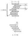
好ましい実施例では、導電性構造体が同じ長さの同一のストリップで構成され、入力手段が、好ましくは、互いに隣接して同じ高さで配置されるこれらのストリップの中心の上を、直線的な線状の動きでスライドする場合、表面センサは、本質的に前記直線的な線状の動きに対応し、それを反映する信号を検出することになる。このように特徴づけられた線状の個々の要素の中央の配置は、本発明ではゼロ位置と呼ばれることが好ましい。このようにして得られた信号を、たとえば表面センサのディスプレイ上に表示することができる。得られた信号は、それを使って時間の関数としての動きの空間的進路を表すことができる、物理学における経路時間図に対応することが好ましいので、時間依存信号と呼ばれることが好ましい。本発明では、たとえば、導電性構造体のすべての線状の個々の要素が、ゼロ位置に存在するとき、本質的に信号の好ましい空間的歪みがないことが好ましい。本発明の好ましい実施例では、好ましくは個々の要素の中心を通って走り、導電性構造体内の電荷キャリア分布の重心線の中心に本質的に対応する事実上の中心線を構築することは、理論的に可能である。 In a preferred embodiment, the electrically conductive structure is made up of identical strips of the same length and the input means are arranged linearly over the centers of these strips which are preferably arranged adjacent to each other and at the same height. When sliding in a linear motion, the surface sensor will detect a signal that essentially corresponds to and reflects said linear linear motion. The central arrangement of the linear individual elements thus characterized is preferably referred to in the present invention as the zero position. The signal thus obtained can be displayed, for example, on the display of the surface sensor. The resulting signal preferably corresponds to the path-time diagram in physics, with which the spatial course of motion as a function of time can be represented, and is therefore preferably referred to as a time-dependent signal. In the present invention, it is preferred that, for example, all linear individual elements of the conductive structure have essentially no preferred spatial distortion of the signal when present in the null position. In a preferred embodiment of the present invention, constructing a virtual centerline, preferably running through the center of the individual elements and corresponding essentially to the center of the centerline of the charge carrier distribution within the conductive structure, is to: Theoretically possible.
本発明の好ましい構成では、導電性構造体の個々の要素は、本質的に互いに平行に配置された長方形に本質的に形成される。導電性構造体が平行に配置されたストリップによって形成される場合、本発明では、仮想中心線が、導電性構造体の外側ストリップの外縁に本質的に垂直であることが好ましい。 In a preferred arrangement of the invention, the individual elements of the electrically conductive structure are essentially formed in rectangles arranged essentially parallel to each other. If the conductive structure is formed by parallel arranged strips, it is preferred in the present invention that the imaginary centerline is essentially perpendicular to the outer edges of the outer strips of the conductive structure.
ただし、ストリップの一部又はすべてが、ゼロ位置に対してシフトされている、すなわちもはや中央に、仮想中心線の周りに配置されていない場合、好ましくは、表面センサで検出される時間依存信号の空間的な歪みがあり得る。たとえば、線状の個々の要素の大部分が、ゼロ位置に対応する導電性構造体の仮想中心線のA側に配置されている場合、時間依存信号は、前記Aの方向にシフトされ、これはたとえば、本発明では、変調、歪み、又は変化と呼ばれる。本発明では、歪みの程度は、個々の要素がゼロ位置に対してどれだけ大きくシフトされているかに依存することが好ましい。ゼロ位置から大きく外れる個々の要素は、好ましくは、時間依存信号の大きい歪みをもたらし、一方ゼロ位置からの小さいずれは、好ましくは小さい歪みをもたらす。 However, if some or all of the strips are shifted with respect to the zero position, i.e. are no longer centrally arranged around the virtual centerline, then preferably the time-dependent signal detected by the surface sensor Spatial distortion is possible. For example, if most of the linear individual elements are located on the A side of the virtual centerline of the conductive structure corresponding to the zero position, the time dependent signal will be shifted in the direction of said A, which is, for example, referred to herein as modulation, distortion, or change. In the present invention, the degree of distortion preferably depends on how much the individual elements are shifted relative to the zero position. Individual elements that deviate significantly from the zero position preferably result in large distortions of the time-dependent signal, while small deviations from the zero position preferably result in small distortions.
入力手段が導電性構造体の複数の個々の要素と同時に接触している場合、個々の要素の歪みの影響は、時間依存信号の生成において有利に重なり、その結果生成された時間依存信号は、カード状物体と入力手段との相対的な動きによって表面センサで検出され得る、導電性構造体の空間的形状を反映する。相対的な動きの、表面センサ上の時間依存信号への変換及び/又は変調は、好ましくは、表面センサを備えるデバイスによって信号を評価する前に行われ、それによりカード状物体の識別を実施できるので有利である。この目的のために、たとえば、検出された時間依存信号又はその空間的進路を、表面センサを備える電子デバイスに保存されているか、又は別のやり方でそれにアクセス可能なデータベースからの、データ(の組)と比較することができる。 When the input means is in contact with multiple individual elements of the conductive structure simultaneously, the strain effects of the individual elements advantageously overlap in producing a time-dependent signal, the resulting time-dependent signal being: It reflects the spatial shape of the conductive structure, which can be detected by the surface sensor by the relative movement of the card-like object and the input means. The conversion and/or modulation of the relative movement into a time-dependent signal on the surface sensor is preferably performed before evaluating the signal by the device with the surface sensor, so that identification of the card-like object can be performed. Therefore, it is advantageous. For this purpose, for example, the detected time-dependent signal or its spatial course is stored in an electronic device comprising a surface sensor, or data (a set of data) from a database otherwise accessible to it. ) can be compared with
さらに好ましい実施例では、導電性構造体が、長さは等しいが幅が異なる線状要素からなり、これらの線状要素が、カード状物体上のその長さに対して中央に配置され、互いから可変距離で配置されて、且つ直線的な線状の動きがカード状物体の中央で発生する場合、その結果得られる静電容量式表面センサ上の時間依存信号は、次のように説明することができる。信号の空間的進路は、本質的に、ほぼ一定のx座標、及び本質的に相対的な動きに対応するy座標の時間に依存する変化によって特徴づけられる。従って、信号の空間的歪みは、本質的にないか、又はほんのわずかである。ただし、その結果得られる時間依存信号は、基準入力に対して、特定の速度プロファイルを持つことが好ましいであろう。入力手段は、カード状物体を横切って移動するとき、カード状物体上の導電性要素と徐々に動作可能に接触するようになる。すなわち、入力手段は、徐々に導電性要素をカバーする。入力手段が導電性の個々の要素に到達すると、結果として生じる信号の位置は、この時点で突然、個々の要素の方向にシフトされる。 In a further preferred embodiment, the electrically conductive structure consists of linear elements of equal length but different widths, which are arranged centrally with respect to their length on the card-like object and is positioned at a variable distance from and linear linear motion occurs in the center of the card-like object, the resulting time-dependent signal on the capacitive surface sensor is described as follows: be able to. The spatial trajectory of the signal is essentially characterized by a nearly constant x-coordinate and a time-dependent change in the y-coordinate that essentially corresponds to relative motion. Therefore, there is essentially no or very little spatial distortion of the signal. However, the resulting time-dependent signal would preferably have a specific velocity profile with respect to the reference input. As the input means moves across the card-like object, it gradually comes into operative contact with the conductive elements on the card-like object. That is, the input means gradually cover the conductive elements. When the input means reaches a conductive individual element, the position of the resulting signal is now abruptly shifted in the direction of the individual element.
具体的な実例では、入力手段は、カード状物体上で、仮想直線に沿ってy方向に均一の速度で移動する。入力手段が導電性要素と接触しない限り、結果として得られた時間依存信号は、本質的にタイム・スタンプ及びそれぞれのy座標が異なるタッチによって好ましくは本質的に特徴づけられ、タッチの速度は本質的に一定である。入力手段が導電性の個々の要素に到達すると、その時点で、結果として得られる信号の位置が突然個々の要素の方向にシフトされる。すなわち、単一のタッチは、前のタッチと比較して、y座標に関してはるかに大きくシフトされる。結果として得られた時間依存信号の個々のタッチのパラメータを使用して、速度プロファイルを計算することができる。本発明では、入力手段が導電性の個々の要素と接触したときに、速度プロファイルの変動を、好ましくは識別することができることが好ましい。 In a concrete example, the input means moves at a uniform speed in the y-direction along an imaginary straight line on the card-like object. As long as the input means are not in contact with the conductive element, the resulting time-dependent signal is preferably characterized essentially by touches with different time stamps and respective y-coordinates, and the speed of the touches is essentially is essentially constant. When the input means reaches a conductive individual element, at that point the position of the resulting signal is abruptly shifted in the direction of the individual element. That is, a single touch is shifted much more with respect to the y-coordinate compared to the previous touch. The individual touch parameters of the resulting time-dependent signal can be used to calculate velocity profiles. In the present invention, it is preferred that variations in the velocity profile can preferably be discerned when the input means are in contact with the conductive individual elements.
「本質的に」という用語は、当業者には不明確ではない。というのは、当業者は、「本質的に長方形によって」形成される導電性構造体は、主に長方形に設計された個々の要素からなり、構造体は、長方形に設計されていないいくつかの個々の要素もまた含むことができることを知っているからである。こうした長方形でない個々の要素は、考えられる任意の形状、たとえば三角形、楕円形、卵形、円形、花形、星形、菱形、又は自由形状を持つことができる。「本質的に平行な」という用語は、導電性構造体の個々の要素が、適用する精度の範囲内で平行に使用されることを意味すると当業者に理解される。たとえば、個々の要素が印刷される場合、個々の要素は印刷精度の範囲内で印刷され、印刷精度がたとえば、平行度が0から2°の程度の大きさからはずれるという結果になる可能性がある。 The term "essentially" is not ambiguous to those skilled in the art. For those skilled in the art will understand that a conductive structure formed "essentially by a rectangle" consists mainly of individual elements of rectangular design, and the structure consists of several non-rectangularly designed elements. Because we know that individual elements can also be included. These non-rectangular individual elements can have any conceivable shape, for example triangular, elliptical, oval, circular, flower-shaped, star-shaped, diamond-shaped or free-form. The term "essentially parallel" is understood by those skilled in the art to mean that the individual elements of the conductive structure are used parallel within the applied precision. For example, when individual elements are printed, the individual elements are printed within printing accuracy, which can result in printing accuracy that deviates from the order of magnitude of, for example, 0 to 2° parallelism. be.
本発明の好ましい実施例では、入力手段と静電容量式表面センサ上のカード状物体との間の相対的な動きから得られる時間依存信号が、カード状物体を使用することなしに生じる入力手段を用いた基準入力によって確立される基準信号に対して変化するような、サイズ、間隔、及び形状に対する導電性構造体の個々の要素を形成することを提供する。 In a preferred embodiment of the invention the time dependent signal resulting from the relative movement between the input means and the card-like object on the capacitive surface sensor is generated without the use of the card-like object. It provides for forming the individual elements of the conductive structure for size, spacing, and shape to vary with respect to a reference signal established by a reference input using .
別の態様において、本発明は、カード状物体に関し、カード状物体は、カード状物体上に配置された複数の個々の要素を具備する導電性構造体を備える。本発明では、カード状物体は、上記の方法を実行するように、又はカード状物体を用いて上述の方法を実行するように適合されることが特に好ましい。本発明の好ましい構成では、導電性構造体の個々の要素は、0.1mmから20mmの幅及び0.1mmから30mmの間隔を持つ。本発明では、6mm以下の幅を持つ導電性構造体、すなわち、たとえば、0.1から6mmの好ましい幅を持つ、導電性構造体を使用することが最も好ましく、本発明では0.1mmから6mmの間のすべての値が好ましい。この寸法の程度は、好ましくは、表面センサが独立した導電性構造体を別の導電性構造体から区別できるように、下げられてはならない(must not be undercut)導電性構造体の限度を表す。従って、本発明の特定の利点は、それを使って導電性構造体が表面センサ上に信号を誘導できる方法及びシステムを提供することであるが、しかし構造体の個々の要素がデータ・キャリア上に単独で配置された場合に、個別に分離された要素が、表面センサで分析及び/又は検出するには小さすぎたため、表面センサで識別することができなかった。結果として、本発明は、先行技術で説明される導電性構造体とは大幅に異なり、表面センサによって確実に識別されるために、構造体の構成要素は通常、たとえば8mmよりも意図的に大きい。表面センサでさえもその構成要素を個別に識別できる導電性構造体の設計は、先行技術ではしばしば「指先の模倣」と呼ばれ、本発明では意図していない。 In another aspect, the invention relates to a card-like object comprising a conductive structure comprising a plurality of individual elements arranged on the card-like object. It is particularly preferred according to the invention that the card-like object is adapted to carry out the above-described method or to carry out the above-described method with the card-like object. In a preferred configuration of the invention, the individual elements of the electrically conductive structure have a width of 0.1 mm to 20 mm and a spacing of 0.1 mm to 30 mm. In the present invention it is most preferred to use conductive structures with a width of 6 mm or less, i.e. with a preferred width of e.g. All values between are preferred. This degree of dimension preferably represents the limit of the conductive structure that must not be undercut so that the surface sensor can distinguish an independent conductive structure from another conductive structure. . A particular advantage of the present invention is therefore to provide a method and system by means of which a conductive structure can induce a signal onto a surface sensor, but the individual elements of the structure can be arranged on a data carrier. When placed singly on the surface sensor, the individually separated elements could not be distinguished by the surface sensor because they were too small to be analyzed and/or detected by the surface sensor. As a result, the present invention differs significantly from the electrically conductive structures described in the prior art, and in order to be reliably identified by surface sensors, the components of the structure are typically intentionally larger than, for example, 8 mm. . The design of conductive structures that can individually identify components of even surface sensors is often referred to in the prior art as "fingertip mimicry" and is not intended for the present invention.
個々の要素のこの意図的に選択された寸法の結果として、導電性構造体は、入力手段とカード状物体との間の相対的な動きによって生成される入力が、時間依存信号に変換され得るように、すなわち、伝導性構造体の個々の要素によって有利にもたらされる歪みに意図的に信号をさらすことにより時間依存信号に変調され得るように、適合されることが、有利にも実現される。導電性構造体の個々の要素は、具体的には、入力手段と動作可能に接触していない単一の個々の要素が、表面センサによって検出及び/又は識別され得ないように構成される。 As a result of this deliberately selected dimensions of the individual elements, the electrically conductive structure allows input generated by relative movement between the input means and the card-like object to be converted into a time dependent signal. so that it can be modulated into a time-dependent signal by deliberately subjecting the signal to distortions that are advantageously brought about by individual elements of the conductive structure. . The individual elements of the electrically conductive structure are specifically configured such that a single individual element that is not in operative contact with the input means cannot be detected and/or identified by the surface sensor.
導電性構造体の個々の構成要素、すなわち入力手段との動作可能な接触がない個々の要素が、静電容量式表面センサ上に信号を生成しない、導電性構造体を提供することができることは、まったく驚くべきことであり、ここで導電性構造体としての要素全体は、驚くべきことに、たとえば、表面センサ上の信号の偏向をもたらすように適合される。カード状物体がない入力手段の基準入力に対して変化することができる時間依存信号の生成は、有利には、その全体でカード状物体の導電性構造体を構成する個々の要素の、相乗的な相互作用によってもたらされる。その個々の要素は表面センサで検出できないか、又は部分的にしか検出できない、表面センサで識別するための導電性構造体を提供することは、先行技術からの新しい発展を示す。これまで、当業者は、表面センサによって読み取られるか又は検出されるべき導電性構造体が、指先の特性をシミュレーションし、個別に分離されて表面センサでやはり検出され得る要素で構成されなければならないと思い込んできた。 It is possible to provide a conductive structure in which individual components of the conductive structure, i.e. individual elements that are not in operable contact with the input means, do not generate a signal on the capacitive surface sensor. , which is quite surprising, wherein the entire element as a conductive structure is surprisingly adapted to effect deflection of the signal on, for example, a surface sensor. The generation of a time-dependent signal that can vary with respect to the reference input of the input means without the card-like object is advantageously the synergistic interaction. Providing a conductive structure for identification with a surface sensor, the individual elements of which are either undetectable or only partially detectable by the surface sensor, represents a new departure from the prior art. Up to now, those skilled in the art have found that a conductive structure to be read or detected by a surface sensor must simulate the properties of a fingertip and consist of elements that can be individually separated and also detected by the surface sensor. I thought.
この点に関して、さらなる態様では、本発明は、入力手段とカード状物体との間の相対的な動きによって、静電容量式表面センサ上に時間依存信号を生成する、カード状物体の使用に関する。上記の時間依存信号を生成する方法及び識別方法の上記の利点と驚くべき技術的効果はまた、カード状物体及びその使用にも適用される。同様に、カード状物体及びその使用の利点と驚くべき技術的効果はまた、識別方法及び信号生成方法にも適用される。これは具体的には、本発明の好ましい実施例に適用され、本発明によれば、静電容量式表面センサ上での時間依存信号の生成は、第1の接点及び第2の接点を提供することを含み、ここでカード状物体と静電容量式表面センサとの間に第1の接点があり、またカード状物体と入力手段との間に第2の接点があり、ここで第1の接点及び第2の接点は同時に存在し、少なくとも第2の接点は動的に形成される。 In this regard, in a further aspect the invention relates to the use of a card-like object in which relative movement between the input means and the card-like object produces a time dependent signal on a capacitive surface sensor. The above advantages and surprising technical effects of the method of generating a time-dependent signal and the method of identification also apply to card-like objects and their uses. Likewise, the advantages and surprising technical effects of card-like objects and their use also apply to identification methods and signal generation methods. This applies in particular to the preferred embodiment of the invention, according to which the generation of the time dependent signal on the capacitive surface sensor provides the first contact and the second contact. wherein there is a first contact between the card-like object and the capacitive surface sensor, and a second contact between the card-like object and the input means, where a first and the second contact exist simultaneously, and at least the second contact is dynamically formed.
この点に関して、好ましくは本発明に関して、時間依存信号が、カード状物体に対する入力手段の動きによって生成され、ここで時間依存信号は、表面センサによって検出され評価され得るという点で、本発明は、情報を個々の要素から抽出することができる従来のデータ・キャリアとは異なる。比較すると、システムは、データ・キャリアと読取デバイスとの間に動きがある先行技術に説明されている。 In this respect, preferably with regard to the invention, the time dependent signal is generated by the movement of the input means relative to the card-like object, where the time dependent signal can be detected and evaluated by a surface sensor. Unlike conventional data carriers where information can be extracted from individual elements. By comparison, systems have been described in the prior art in which there is movement between the data carrier and the reading device.
本発明では、入力手段と静電容量式表面センサ上のカード状物体との間の相対的な動きから得られる時間依存信号が、カード状物体を使用することなしに生じる入力手段を用いた基準入力に対して変化するような、サイズ、間隔、及び形状に対するカード状物体の導電性構造体の個々の要素が形成されることが特に好ましい。 In the present invention, the time-dependent signal resulting from the relative movement between the input means and the card-like object on the capacitive surface sensor is a reference using the input means that occurs without the use of the card-like object. It is particularly preferred that the individual elements of the conductive structure of the card-like body are formed for size, spacing and shape to vary with input.
本発明では、少なくとも2つの個々の要素が、相対的な動きがある任意の時点で、少なくとも部分的に入力手段と動作可能に接触するような、サイズ、間隔及び形状に対する導電性構造体の個々の要素が寸法決めされることが特に好ましい。入力手段は、たとえば、指又は伝導性物体であり得る。この場合、少なくとも2つの個々の要素を、導電性構造体の仮想中心線に対して同一又は異なる方向に向けることができ、ここで個々の要素の相異なる方向は、好ましくは、時間依存信号に相異なる歪み効果をもたらし、一方、同一の方向は、好ましくは、本質的に等しい歪み効果をもたらす。相異なる歪み効果の場合、こうした効果が重なり合う可能性があり、その結果生成される信号は、好ましくは、導電性構造体の空間構造、具体的には平面状のカード状物体上の個々の要素の配置を反映する。 In the present invention, each of the electrically conductive structures is sized, spaced and shaped such that at any time there is relative movement, at least two individual elements are at least partially in operable contact with the input means. It is particularly preferred that the elements of are dimensioned. The input means can be, for example, a finger or a conductive object. In this case, at least two individual elements can be oriented in the same or different directions with respect to the virtual centerline of the conductive structure, wherein the different orientations of the individual elements are preferably directed to the time-dependent signal. Different distortion effects are produced, while the same orientation preferably produces essentially equal distortion effects. In the case of different distortion effects, such effects may overlap, and the resulting signal is preferably the spatial structure of the conductive structure, in particular the individual elements on a planar card-like object. reflect the placement of
本発明のさらなる好ましい構成では、サイズ、間隔、及び形状に対する導電性構造体の個々の要素は、相対的な動きがある任意の時点で、多くとも1つの個々の要素が、指又は伝導性物体と動作可能に接触するように寸法決めされる。個々の要素間の間隔が増加するために、生成された時間依存信号は、好ましくは、ゼロ位置に戻される。信号の評価については、この種の配置により、入力手段による相対的な動きの特に単純で明確な識別が、従って好ましくは、信号パターンのより正確な判断が可能になる。この実施例の別の利点は、複数の個々の要素による歪み効果の重なり合い、及び表面センサを備える電子デバイス内の信号の評価における、結果として生じる曖昧さを回避することである。 In a further preferred arrangement of the invention, the individual elements of the electrically conductive structure with respect to size, spacing and shape are such that at any time there is relative movement at most one individual element is a finger or a conductive object. sized to be in operable contact with the Due to the increasing spacing between the individual elements, the generated time dependent signal is preferably returned to the zero position. For signal evaluation, an arrangement of this kind allows a particularly simple and unambiguous identification of relative movements by the input means and thus, preferably, a more accurate determination of the signal pattern. Another advantage of this embodiment is that it avoids the superimposition of distortion effects from multiple individual elements and the resulting ambiguity in evaluating signals in electronic devices with surface sensors.
入力は、たとえば1本又は複数の指又は導電性物体などの入力手段を用いて行われ、好ましくはカード状物体に対して動くが、カード状物体は静電容量式表面センサに対して動かないことが、さらに好ましい。他の用途では、入力は、入力手段、たとえば1本又は複数の指又は導電性物体を用いて行われ、カード状物体に対して動くが、一方指は、静電容量式表面センサに対して動かず、またカード状物体は、入力手段と静電容量式表面センサとの間を動くことが好ましい場合がある。 Input is made using input means, for example one or more fingers or a conductive object, which preferably moves relative to the card-like object, but the card-like object does not move relative to the capacitive surface sensor. is even more preferred. In other applications, input is made using an input means, such as one or more fingers or a conductive object, which moves relative to the card-like object, while the fingers move against a capacitive surface sensor. It may be preferred that it does not move and the card-like object moves between the input means and the capacitive surface sensor.
時間依存信号は、好ましくは、タイム・スタンプ情報ばかりでなく、x座標及びy座標を使って表すことができる。時間依存信号の空間的進路は、たとえば、波状、連続的、線に沿った、及び/又は上下であり得るが、それに限定されるものではない。この場合、空間的進路は、本質的に個々の要素の構造及び/又は配置に従うことが好ましい。導電性構造体が、たとえば横断歩道のように本質的に隣同士平行に配置された長方形の線状の個々の要素からなる場合、ストリップの短い方の辺は、ストリップ間の間隙によって分断される導電性構造体の外側の線を形成する。導電性構造体の外側の線は、すべての個々の要素が同じ開始位置及び/又は終了位置を持っている場合、横断歩道のように直線になり得る。個々の要素もすべて同じ長さである場合、結果的に、好ましくは、本質的に平行な外側の線を持つ長方形の導電性構造体となる。 Time-dependent signals can preferably be represented using x- and y-coordinates as well as time stamp information. The spatial course of the time-dependent signal can be, for example, but not limited to, wavy, continuous, along a line, and/or up and down. In this case, the spatial course preferably follows essentially the structure and/or arrangement of the individual elements. If the conductive structure consists essentially of rectangular linear individual elements arranged parallel to each other, such as a pedestrian crossing, the shorter sides of the strips are separated by the gaps between the strips. Form the outer lines of the conductive structure. The outer line of the conductive structure can be straight like a pedestrian crossing if all individual elements have the same start and/or end position. If the individual elements are also all of the same length, the result is preferably a rectangular conductive structure with essentially parallel outer lines.
個々の要素を形成する長方形のストリップが同じ開始位置及び終了位置を持たず、且つ/又は異なる長さを持つ場合、外側の線を、たとえば波状に構成することができる。本発明では、生成される時間依存信号は、特にこうした外側の線又はその重なり合いの進路を反映することが好ましく、ここで時間依存信号の空間的進路を、たとえば、表面センサのディスプレイ上で見えるようにすることができる。本発明のある適用例では、時間依存信号の進路が区分ごとに偏向されず、カード状物体上の入力手段の動きに従うことが好ましい場合がある。かかる用途は、たとえば、導電性構造体の複数の領域を備えるカード状物体である。たとえば、各領域は、電子デバイス上の異なる作用に関連づけられる。個々の領域間の、個々の領域の識別が曖昧な場合の時間依存信号は、区分ごとに偏向されないことが好ましい。切れ目のないかかる区分を用いて、カード状物体上の各区分の絶対位置もまた判断できることは有利である。 If the rectangular strips forming the individual elements do not have the same start and end positions and/or have different lengths, the outer lines can be constructed, for example wavy. In the present invention, the generated time-dependent signal preferably reflects in particular the course of such outer lines or their overlapping, where the spatial course of the time-dependent signal is e.g. visible on the display of the surface sensor. can be In some applications of the invention, it may be preferable that the path of the time-dependent signal is not deflected segment by segment, but follows the movement of the input means on the card-like object. Such applications are, for example, card-like objects comprising multiple regions of electrically conductive structures. For example, each region is associated with a different action on the electronic device. Preferably, the time-dependent signal between the individual regions, where the identification of the individual regions is ambiguous, is not biased segment by segment. Advantageously, with such unbroken segments, the absolute position of each segment on the card-like object can also be determined.
本発明では、入力手段とカード状物体との間、並びにカード状物体と表面センサとの間の、同時に形成される動作可能な接触は、静電容量式であることが特に好ましい。入力手段とカード状物体との間の動作可能な接触が、電気的な接続を構成することが好ましい場合もある。静電容量式動作接点には、入力手段と導電性構造体との間に電気的接続が存在する必要がないという利点がある。すなわち、導電性構造体を、たとえば、ラッカ、色層、印刷されたグラフィック、ラベル若しくはステッカ、及び/又は別の層でカバーすることができる。これにより、導電層を光学的にカバーし、カード状物体の表面を伝導性構造体とは独立して魅力的にすることが可能になる。加えて、導電層を機械的摩耗から有利に保護することができ、長期間の使用中に、より信頼性の高い機能を保証することができる。これは、導電性構造体を、それぞれのカード形状の物体の識別機能として、好ましくは完全に光学的及び触覚的に隠すことができるので、先行技術に対する明確な利点を示す。先行技術では、たとえば、カメラ又は光センサを用いて光学的に読み取られるバーコードが知られており、従って、バーコードは本質的に可視であり、製品の外観に影響を与える可能性がある。さらに、RFIDタグが先行技術で知られており、それは本質的にアンテナ及び使用されるチップからなる。こうしたタグは、より薄い、且つ/又は柔軟な材料内に一体化することもできるが、チップは所定の最小の厚みを持っているので、目立つことが多い。 It is particularly preferred according to the invention that the simultaneous operable contacts between the input means and the card-like object and between the card-like object and the surface sensor are capacitive. It may be preferred that the operable contact between the input means and the card-like object constitutes an electrical connection. Capacitive actuation contacts have the advantage that no electrical connection needs to exist between the input means and the conductive structure. That is, the electrically conductive structure can be covered with, for example, lacquers, colored layers, printed graphics, labels or stickers, and/or further layers. This makes it possible to optically cover the conductive layer and make the surface of the card-like object attractive independently of the conductive structure. In addition, the conductive layer can be advantageously protected against mechanical wear, ensuring a more reliable function during long-term use. This presents a distinct advantage over the prior art, as the electrically conductive structures can be hidden, preferably completely optically and tactilely, as an identifying feature of the respective card-shaped object. In the prior art, bar codes are known that are read optically, for example using a camera or a light sensor, and thus bar codes are inherently visible and can influence the appearance of the product. Furthermore, RFID tags are known in the prior art, which essentially consist of an antenna and a chip used. Such tags can be integrated into thinner and/or flexible materials, but the chip has a certain minimum thickness and is often conspicuous.
さらに、導電性構造体は、箔転写法、たとえば、こうした適用方法に限定されるものではないが、冷箔転写、ホット・スタンプ、及び/又は熱転写を用いて、好ましくはカード状物体の可撓性の基板材料に適用することができる。具体的には、オフセット印刷、グラビア印刷、フレキソ印刷、及び/又はスクリーン印刷、並びに/或いは、たとえば金属粒子、ナノ粒子、炭素、グラフェン及び/又は導電性ポリマーをベースとする導電性インクを使用するインクジェット法などの印刷方法を、カード状物体の生産に使用することができるが、こうした印刷方法及び/又は材料に限定されるものではない。本発明では、導電性構造体を少なくとも1つのさらなる層を使ってカバーすることも好ましい場合があり、この層は、紙ベース又は箔ベースのラミネート材料又は少なくともラッカ/インク層であり得る。この層は、光学的に透明でも不透明でもよい。 Further, the electrically conductive structure is preferably formed into a flexible card-like object using foil transfer methods, such as, but not limited to, cold foil transfer, hot stamping, and/or thermal transfer. It can be applied to any substrate material of any type. In particular using offset printing, gravure printing, flexographic printing and/or screen printing and/or conductive inks based on e.g. metal particles, nanoparticles, carbon, graphene and/or conductive polymers Printing methods such as inkjet methods can be used to produce card-like objects, but are not limited to such printing methods and/or materials. It may also be preferred according to the invention to cover the electrically conductive structure with at least one further layer, which may be a paper-based or foil-based laminate material or at least a lacquer/ink layer. This layer may be optically transparent or opaque.
本質的に類似した個々の要素の、その好ましい構造体であるため、導電性構造体が特に容易に個別化できることは、まったく驚くべきことであった。 It was quite surprising that the electrically conductive structure is particularly easy to individualize due to its preferred structure of essentially similar individual elements.
伝統的な従来の印刷方法の特徴は、印刷されるべきモチーフが、グラビア・シリンダ又はオフセット印刷版などの印刷フォームに適用され、複数回高速で複製されるという点で、モチーフの単純で迅速な複製である。従来の印刷方法は、個別化されるコンテンツの生産には適さない。というのは、印刷フォームの作成が、総生産コストのかなりの割合を占めるからである。従って、経済的に生産できるのは、より大量の印刷製品だけである。グラフィック印刷では、個々のコンテンツを経済的に印刷可能な、個別化される製品だけでなく、少量生産向けのデジタル印刷方法が存在する。こうした印刷方法は、たとえば、電子写真、レーザ印刷、又はインクジェット印刷を含む。現在、かかるデジタル印刷方法を使用して経済的に導電性要素を生産することは不可能である。しかし、従来の印刷方法及びそれに加える又は減ずる方法の、方法の組合せにより、個別化された導電性構造体を生産することが可能である。以下では、2つの可能な生産プロセスの概要を説明する。 A characteristic of traditional conventional printing methods is the simple and rapid transfer of motifs in that the motif to be printed is applied to a printing form such as a gravure cylinder or an offset printing plate and replicated multiple times at high speed. It is a copy. Conventional printing methods are not suitable for producing personalized content. This is because the creation of printed forms represents a significant percentage of the total production cost. Therefore, only larger quantities of printed products can be produced economically. In graphics printing, there are digital printing methods for low volume production as well as individualized products that can economically print individual content. Such printing methods include, for example, electrophotography, laser printing, or inkjet printing. Currently, it is not possible to economically produce conductive elements using such digital printing methods. However, it is possible to produce individualized conductive structures by a combination of methods, conventional printing methods and methods in addition or subtraction. In the following, two possible production processes are outlined.
レーザ切除
第1のステップでは、導電性塗料又は箔転写法によって、導電性基本構造体が、たとえば可撓性基板に塗布される。基本構造体は、たとえば均一な等距離の個々の要素、たとえば長方形で構成される。第2のプロセスのステップでは、導電性の個々の要素は、レーザ切除によって所定の場所で互いから電気的に分離される。すなわち、こうした場所で、導電性材料が選択的に取り除かれる。これにより、固有の、すなわち個別化された構造体を、効率的に生産することができる。この生産方法の驚くべき利点は、導電性構造体の優れた光学的隠蔽性である。ラミネート又はラベルを用いて導電性構造体を重ね刷り又はカバーした後でさえも、導電性構造体が、場合によっては、バックライト条件下で人間の目に見える場合がある。構造体が表面全体に分布し、薄いレーザ切断によって所定の場所だけで分離されている場合、この構造体を肉眼で識別するのは、はるかに困難である。Laser Ablation In a first step, an electrically conductive base structure is applied to a flexible substrate, for example, by means of a conductive paint or foil transfer method. The basic structure consists, for example, of uniform equidistant individual elements, for example rectangles. In a second process step, the conductive individual elements are electrically isolated from each other at predetermined locations by laser ablation. That is, the conductive material is selectively removed at these locations. This allows unique or individualized structures to be efficiently produced. A surprising advantage of this production method is the excellent optical hiding of the conductive structures. Even after overprinting or covering the conductive structures with a laminate or label, the conductive structures may still be visible to the human eye under backlight conditions in some cases. If the structures were distributed over the surface and separated only at certain locations by thin laser cuts, they would be much more difficult to discern with the naked eye.
従って、さらに好ましい構成では、本発明は、カード状物体に関し、ここで導電性構造体は、以下のステップを含む多段階のプロセスで生産される。
a)箔転写法又は導電性塗料を用いて、導電性基本構造体を基板に塗布するステップ。
b)レーザを用いて導電性基本構造体の一部を選択的に取り除くステップであって、それによって空間的に分離された領域を具備する個々の要素を備えた導電性構造体が得られるステップ。Therefore, in a further preferred arrangement, the invention relates to a card-like object, wherein the electrically conductive structure is produced in a multi-step process comprising the following steps.
a) Applying a conductive base structure to the substrate using a foil transfer method or conductive paint.
b) using a laser to selectively remove portions of the conductive base structure, thereby resulting in a conductive structure with individual elements having spatially separated regions; .
さらに好ましい実施例では、本発明は、カード状物体に関し、ここで導電性構造体は、多段階のプロセスで生産することができ、ここで多段階のプロセスは、好ましくは以下のステップを含む。
a)導電性基板材料、たとえば金属箔若しくは金属板、金属化された紙、及び/又はアルミニウム被覆箔を供給するステップ。
b)レーザを用いて導電性コーティングの一部を選択的に取り除くステップであって、それによって空間的に分離された領域を具備する個々の要素を備えた導電性構造体が得られるステップ。In a further preferred embodiment, the invention relates to a card-like object, wherein the electrically conductive structure can be produced in a multi-step process, wherein the multi-step process preferably comprises the following steps.
a) providing an electrically conductive substrate material, such as metal foil or metal plate, metallized paper and/or aluminum coated foil.
b) Using a laser to selectively remove portions of the conductive coating, thereby resulting in a conductive structure with individual elements having spatially separated regions.
本発明では、「レーザを用いて」という用語は、好ましくは、レーザ放射が、以前に適用されていた導電性基本構造体の選択された場所で、導電性材料を切除するために使用されることを意味する。その結果、基本構造体の、以前は連続した導電性の個々の要素に切れ目が形成され、切れ目が個々の要素の2つの部分領域間の電気的接続を有利に分断し、それにより、たとえば個々の要素の長さを調整することができる。その結果、個々の要素を備えた導電性構造体を生産することができ、ここで導電性構造体の個々の要素は、空間的に分離された領域を具備する。有利には、個々の要素の面積もまた設定することができ、入力手段とカード状物体との間に相対的な動きがある場合、表面センサによって検出することができる。本発明では、基板は、可撓であるよう設計されることが好ましい。たとえば、基板は、非常に薄い設計のプラスチック、厚紙、及び/又は紙カードであり得るので、可撓性であり、特に印刷機内で処理するのが特に容易で、すなわち印刷することができる。かかるカードは、名刺又はデビット・カードの好ましいサイズの範囲にあることが特に好ましい。 In the present invention, the term "with a laser" is preferably used to ablate electrically conductive material at selected locations of a previously applied electrically conductive base structure where laser radiation has been applied. means that As a result, a discontinuity is formed in the previously continuous, electrically conductive individual element of the basic structure, the discontinuity advantageously disrupting the electrical connection between two partial regions of the individual element, thereby e.g. You can adjust the length of the elements of As a result, an electrically conductive structure with individual elements can be produced, where the individual elements of the electrically conductive structure comprise spatially separated regions. Advantageously, the area of the individual elements can also be set and can be detected by surface sensors if there is any relative movement between the input means and the card-like object. In the present invention, the substrate is preferably designed to be flexible. For example, the substrate may be a plastic, cardboard and/or paper card of very thin design, so that it is flexible and particularly easy to process, ie printable, in a printing machine. It is particularly preferred that such cards be in the preferred size range of business cards or debit cards.
インクジェット印刷
導電性構造体の遡及的な個別化の別の可能性は、導電性ブリッジの遡及的適用である。第1のステップでは、導電性塗料又は箔転写法によって、導電性基本構造体が、たとえば可撓性基板に塗布される。基本構造体は、好ましくは、等距離の個々の要素、たとえば、所定の場所に切れ目がある長方形からなる。第2のプロセスのステップでは、こうした切れ目が導電性塗料を用いて選択的に印刷され、それによって相互接続される。また、このプロセスでは、固有の、すなわち個別化された導電性構造体を効率的に生産することができる。Inkjet printing Another possibility for retrospective individualization of conductive structures is the retroactive application of conductive bridges. In a first step, a conductive base structure is applied to a flexible substrate, for example, by means of conductive paint or a foil transfer method. The basic structure preferably consists of equidistant individual elements, for example rectangles with cuts at predetermined places. In a second process step, these cuts are selectively printed with conductive paint and thereby interconnected. Also, the process can efficiently produce unique or individualized conductive structures.
従って、さらに好ましい構成では、本発明は、カード状物体に関し、導電性構造体は、以下のステップを含む多段階のプロセスで生産される。
a)箔転写法又は導電性塗料を用いて、導電性基本構造体を基板に塗布するステップ。
b)導電性塗料をカード状物体に塗布するのに用いられるインクジェット印刷によって、導電性ブリッジ及び/又は追加の導電性要素を選択的に塗布するステップであって、それによって個々の要素を備える導電性構造体が得られるステップ。Therefore, in a further preferred arrangement, the invention relates to a card-like object, the electrically conductive structure being produced in a multi-step process comprising the following steps.
a) Applying a conductive base structure to the substrate using a foil transfer method or conductive paint.
b) selectively applying conductive bridges and/or additional conductive elements by ink-jet printing, which is used to apply conductive paint to card-like objects, thereby forming a conductive layer comprising individual elements; A step in which a sexual structure is obtained.
本発明のこの好ましい実施例では、「基板」という用語は、好ましくは、本発明の上記構成のものと理解される。本発明の本実施例では、導電性基本構造体が、切れ目を持つ個々の要素を備えることが特に好ましい。本発明では、こうした切れ目は、好ましくは個々の要素内の間隙であり、ここでそれぞれの個々の要素は、好ましくは1つ又は複数の切れ目を持つ。こうした切れ目が、それぞれの個々の要素内の電気的接続を分断することが特に好ましい。本発明では、導電性ブリッジは、好ましくは、以前に切れ目で分離された個々の要素の領域間に電気接続を確立するという意味で、切れ目に打ち勝つ導電性物体である。かかる導電性ブリッジは、インクジェット印刷を用いてカード状物体に導電性塗料を塗布することによって生成され、それによって、有利なことに個々の要素を備える導電性構造体が得られ、その中で以前に適用された基本構造体の切れ目にブリッジが打ち勝ち、個々の要素の2つの部分領域間に、以前は存在しなかった接続を生成することができる。新しく作成された接続は、電気的だけでなく、静電容量的でもあり得る。本発明では、導電性ブリッジ及び/又は追加の導電性要素が、他の塗布器を使用してカード状物体に塗布されることが好ましい場合もある。 In this preferred embodiment of the invention, the term "substrate" is preferably understood as that of the above-described configuration of the invention. In this embodiment of the invention, it is particularly preferred that the electrically conductive base structure comprises individual elements with discontinuities. In the present invention, such discontinuities are preferably gaps within individual elements, where each individual element preferably has one or more discontinuities. It is particularly preferred that such discontinuities disrupt electrical connections within each individual element. In the present invention, a conductive bridge is preferably a conductive object that overcomes a discontinuity in the sense that it establishes an electrical connection between regions of individual elements previously separated by a discontinuity. Such conductive bridges are produced by applying a conductive paint to a card-like object using inkjet printing, thereby advantageously resulting in a conductive structure comprising individual elements, in which the previous A bridge can overcome a discontinuity in a basic structure applied to , creating a previously non-existent connection between two sub-regions of an individual element. The newly created connection can be capacitive as well as electrical. It may be preferred in the present invention that the conductive bridges and/or additional conductive elements are applied to the card-like object using another applicator.
さらなる実施例では、導電性基本構造体は、個々の要素を備える。こうした個々の要素を、インクジェット印刷を使って、それぞれの個々の要素に隣接して少なくとも0.2mmだけ重なり合う追加の導電性材料を印刷することにより、一方向又は両方向に延ばすことが好ましい。かかる追加の導電性要素を塗布することにより、導電性基本構造体を、特に簡単なやり方で変更することができる。 In a further embodiment, the electrically conductive base structure comprises individual elements. These individual elements are preferably extended in one or both directions by printing additional conductive material adjacent to each individual element and overlapping by at least 0.2 mm using inkjet printing. By applying such additional electrically conductive elements, the electrically conductive base structure can be modified in a particularly simple manner.
本発明では、最初に生成された導電性基本構造体の遡及的加工を「個別化する」と呼ぶことが好ましい。これは、好ましくは、それぞれが異なる導電性構造体を備えるカード状物体を生成することができることを意味し、この差を、好ましくは、表面センサが識別することができ、その結果たとえば、相異なるデータ(の組)及び/又は相異なる作用を、表面センサを備える電子デバイス内の相異なるカード状物体に割り当てることができる。こうした後加工プロセスにより、以前は経済的な方法で行うことが不可能であった、特に高速で費用対効果の高い簡単なやり方で、カード状物体を個別化することが可能になったことはまったく驚くべきことであった。 In the context of the present invention, the retrospective processing of the originally produced electrically conductive base structures is preferably referred to as "individualizing". This preferably means that card-like objects can be produced, each with a different electrically conductive structure, this difference preferably being discernible by the surface sensor, so that for example different Data (sets) and/or different actions can be assigned to different card-like objects in an electronic device with a surface sensor. Such post-processing processes have made it possible to individualize card-like objects in a particularly fast, cost-effective and easy manner, which was previously impossible to do in an economical manner. It was quite astonishing.
さらなる態様では、本発明は、カード状物体及び静電容量式表面センサを備えるシステムに関し、ここでカード状物体は静電容量式表面センサ上に置くことができ、カード状物体は、入力手段とカード状物体との間の相対的な動きによって時間依存信号を生成するように適合され、ここで時間依存信号は、カード状物体上の個々の要素の配置によって確立することができる。この方法及びカード状物体に関して説明される定義、技術的効果、及び利点は、システムにも同様に適用され、逆も同様である。本発明のこの実施例では、入力デバイスと静電容量式表面センサ上のカード状物体との間の相対的な動きから得られる時間依存信号が、カード状物体を使用することなしに生じる入力手段を用いた基準入力に対して変化するような、サイズ、間隔、及び形状に対する導電性構造体の個々の要素が形成されることが特に好ましい。 In a further aspect, the invention relates to a system comprising a card-like object and a capacitive surface sensor, wherein the card-like object can be placed on the capacitive surface sensor, the card-like object being an input means and a capacitive surface sensor. It is adapted to generate a time-dependent signal by relative movement with the card-like object, where the time-dependent signal can be established by the arrangement of individual elements on the card-like object. The definitions, technical effects, and advantages described with respect to the method and card-like object apply equally to the system, and vice versa. In this embodiment of the invention, the time dependent signal resulting from the relative movement between the input device and the card-like object on the capacitive surface sensor is an input means that occurs without the use of the card-like object. It is particularly preferred that the individual elements of the conductive structure are formed for size, spacing and shape that vary with respect to a reference input using .
本発明では、このシステムは、第1の接点及び第2の接点によって特徴づけられ、第1の接点はカード状物体と静電容量式表面センサとの間に存在し、第2の接点はカード状物体と入力手段との間に存在し、ここで少なくとも第2の接点は動的に形成されることが特に好ましい。本発明では、第2の接点の動的な形成は、入力手段とカード状物体との間の相対的な動きに対応することが好ましい。 According to the invention, the system is characterized by a first contact and a second contact, the first contact being between the card-like object and the capacitive surface sensor, and the second contact being the card. It is particularly preferred that a contact is present between the object and the input means, wherein at least the second contact is dynamically formed. According to the invention, the dynamic formation of the second contact preferably corresponds to relative movement between the input means and the card-like object.
打抜きなど、外形を変更することによって個々の要素を構造化する
個々の要素の柔軟な配置により、驚くべきことに、個々の要素のそれぞれに必要なサイズ、間隔、及び形状を、印刷プロセスの代替として、又は印刷プロセスに加えて、既存の生産方法で特に経済的に生産することができる、本発明のさらなる実施例という結果がもたらされる。従って、既存の導電性構造体又は表面を、個々の要素が本発明に従って時間依存信号を生成できるように、たとえば所定のミシン目線に沿って、打抜き、切断、レーザ切断、及び/又は引裂きによって生産することが考えられる。従って、とりわけ金属化された箔又はホログラムなどの既存の導電性材料を、遡及的に、且つ高い費用対効果で構造化し、本発明の個々の要素を形成することも可能である。本発明の対応する実施例を、図19に示す。Structuring the individual elements by changing their outer shape, such as punching Flexible placement of the individual elements surprisingly allows the required size, spacing and shape of each individual element to be used as an alternative to the printing process. The result is a further embodiment of the invention which can be produced particularly economically with existing production methods as or in addition to the printing process. Thus, existing conductive structures or surfaces are produced by punching, cutting, laser cutting and/or tearing, for example along predetermined perforation lines, such that individual elements can generate time dependent signals according to the invention. can be considered. Thus, it is also possible to retroactively and cost-effectively structure existing electrically conductive materials, such as metallized foils or holograms among others, to form the individual elements of the invention. A corresponding embodiment of the invention is shown in FIG.
光学設計としての、又はたとえば機能の組合せによる、他の機能を使用可能にするための、個々の要素の配置及び構成
本発明の著しい利点は、驚くべきことに、個々の要素の非常に柔軟なサイズ、間隔及び形状から生じる。従って、こうした導電性の個々の要素をまた、ユーザに見えるようにして、たとえば、所定の記号、標識、又はデザインの形で配置することもできる。1つのあり得る用途は、たとえば、マーケティング資料上の導電性の個々の要素からなる会社のロゴ、及び/又は本発明による紙幣上の、個々の要素からなるホログラムなどの安全機能であり得る。特に安全関連の用途では、たとえば箔転写法において導電性アルミニウムを使って適用されるホログラムに利用可能な材料を使って、本発明による個々の要素を生産することができる。ここでの大きな利点は、結果として生じる信号が静電容量的に検出され、直接の電気的接触が不要なことである。驚くべきことに、たとえばホログラムの場合、機械的摩耗から保護するために、箔又はラッカを用いてカバーされる材料を使用することもまた可能である。さらに、個々の要素を、他の電子的な機能に従って配置し、従って、たとえば、アンテナ又は導電性トラックとして形成することもできる。Arrangement and configuration of the individual elements as an optical design or to enable other functions, e.g. It arises from size, spacing and shape. Such electrically conductive individual elements can thus also be visible to the user and arranged, for example, in the form of predetermined symbols, markings or designs. One possible application could be, for example, a safety feature such as a conductive discrete element company logo on marketing materials and/or a discrete element hologram on banknotes according to the invention. Especially for safety-related applications, the individual elements according to the invention can be produced using materials available for holograms, which are applied using conductive aluminum in the foil transfer method, for example. The big advantage here is that the resulting signal is detected capacitively, no direct electrical contact is required. Surprisingly, it is also possible, for example in the case of holograms, to use materials that are covered with foil or lacquer in order to protect against mechanical wear. Furthermore, the individual elements can also be arranged according to other electronic functions and thus formed, for example, as antennas or conductive tracks.
本発明では、本発明に従って時間依存信号を生成する個々の要素が、他の機能を同時に満たすことができることにより、生産において多くの効率の向上及びコスト節約が可能であることは、まったく驚くべきことであった。逆に、本発明では、既存のホログラム又は他の安全要素を個別に、又は追加で適用される導電性構造体と組み合わせて静電容量的に評価するか、或いはたとえばレーザ又はインクジェットを用いて、導電性構造体を遡及的に修正し、表面センサ上で結果として得られ評価され得る特定の信号を生成することが好ましい場合もある。先行技術では、導電性構造体による別個の機能のみがこれまでに知られてきたが、ここにあるような好都合の特性のかかる組合せは知られていない。ある得る用途の1つは、たとえば、RFID又はNFCタグとプラスチック・カード内のこのデバイスとの組合せであり、RFID/NFCタグは、好ましくは、識別のために使用され、デバイスは、好ましくは、たとえばタブレットなどの静電容量式表面センサ上での相互作用のさらなる識別を可能にする。本発明の対応する実施例を、図20に示す。 In the present invention, it is quite surprising that many efficiency gains and cost savings in production are possible due to the individual elements that generate time-dependent signals according to the invention being able to fulfill other functions at the same time. Met. Conversely, in the present invention, existing holograms or other security elements are evaluated capacitively, either individually or in combination with additionally applied conductive structures, or by e.g. It may be preferable to retroactively modify the conductive structure to produce a specific signal that can be evaluated as a result on the surface sensor. The prior art has hitherto known only separate functions by conductive structures, but not such a combination of advantageous properties as here. One possible application is for example the combination of an RFID or NFC tag and this device in a plastic card, the RFID/NFC tag preferably being used for identification and the device preferably Allows further discrimination of interactions on capacitive surface sensors, eg tablets. A corresponding embodiment of the invention is shown in FIG.
相異なる電気的特性を持つ材料の組合せ
本発明の別の驚くべき利点は、異なる導電性の材料の組合せから生じる。カード状物体の1つ又は複数の個々の伝導性要素を、相異なる電気的特性を持つ材料から完全に、部分的に、及び/又は混ぜて生成することは、すべて同じ導電性材料で生産された、かかる伝導性の個々の要素と比較して、時間依存信号の異なる変調という結果をもたらす。これは、目に見える導電性構造体からの時間依存信号の変調を推定することはもはや不可能なので、具体的には、紙幣、身分証明書、支払機能、及び/又は識別機能などの安全関連の適用例にとって、大きな利点である。図21は、2つの光学的に同一の伝導性構造体及びその信号の進路を比較して示しており、ここで一方の構造体内において、いくつかの個々の要素が、相異なる電気的特性を持つ材料から全体的又は部分的に生産された。Combination of Materials with Different Electrical Properties Another surprising advantage of the present invention arises from the combination of materials with different electrical conductivity. Making one or more of the individual conductive elements of the card-like object entirely, partially and/or intermingled from materials with different electrical properties is all produced from the same conductive material. It also results in a different modulation of the time dependent signal compared to individual elements of such conductivity. This is particularly the case for security-related applications such as banknotes, identification cards, payment functions and/or identification functions, since it is no longer possible to estimate the modulation of time-dependent signals from visible conductive structures. This is a great advantage for the application of FIG. 21 shows a comparison of two optically identical conductive structures and their signal paths, where within one structure several individual elements exhibit different electrical properties. produced wholly or partly from materials
非機能的な混同(confusion)パターンとしての導電性構造体
図22は、導電性構造体を備えるカード状物体を示し、さらに、第1の構造体から電気的に分離された別の伝導性構造体が、光学的混同パターンとして使用される。本発明によれば、導電性の個々の要素ばかりでなく光学的混同構造体が、機能性に影響を与えることなく同じ材料で構成できることは、驚くべき利点であることを証明している。従って、本発明の実際の構造体は光学的に識別するのがより難しいので、あり得る用途は、たとえば、紙幣又は身分証明書又はコピー防止、或いはその組合せの分野であり得る。Conductive Structures as Non-Functional Confusion Patterns FIG. 22 shows a card-like object comprising conductive structures and further conductive structures electrically isolated from the first structure. A body is used as an optical confusion pattern. According to the present invention, it proves to be a surprising advantage that the electrically conductive individual elements as well as the optically mixed structure can be constructed of the same material without affecting the functionality. The actual structure of the invention is therefore more difficult to optically discern, so that possible applications could be, for example, in the fields of banknotes or identification or copy protection, or a combination thereof.
同じ導電性構造体で異なる信号を生成する個々の移動経路
図23は、その上に導電性構造体が配置されたカード状物体を示し、この物体には、可能な動作経路にマークがついている。入力は、好ましくは、複数のこうしたマーク間の入力手段の相対的な動きによって行われる。ユーザが選択した動作経路に応じて、異なる時間依存信号が生成される。1つのあり得る適用例は、たとえば、個別に選択されたジェスチャに基づいて、IDカード及び/又は支払カードなどのキャリア媒体を介してパスワードを入力することであり得る。本発明では、たとえば、スマートフォンのロック解除について知られているようなかかるジェスチャが、たとえば、2因子認証の意味で実現が容易なカード形状の物体と組み合わせて、さらなる個別キーとして機能することができることは、特に驚くべきことであった。Individual movement paths that produce different signals with the same conductive structure Figure 23 shows a card-like object with conductive structures placed thereon, the object being marked with the possible paths of movement. . Input is preferably effected by relative movement of the input means between a plurality of such marks. Different time dependent signals are generated depending on the motion path selected by the user. One possible application could be, for example, entering a password via a carrier medium such as an ID card and/or payment card based on an individually selected gesture. According to the invention, such a gesture, as it is known for example for unlocking smartphones, can serve as a further individual key, for example in combination with a card-shaped object, which is easy to implement in the context of two-factor authentication. was particularly surprising.
物体の周りに個々の要素を配置すること
図24は、少なくとも部分的に別の物体に巻きつけられた導電性構造体を備える、カード状物体を示す。この場合、導電性構造体は、第1の能動的接点及び第2の能動的接点がそれぞれ、巻きつけられた物体の2つの相異なる側部又は平面上に生じるよう構成された。あり得る用途は、たとえば、遡及的に貼りつけられた識別ラベルを用いた身分証明書、又は特に厚い基板、又はパッケージ、或いはその組合せの識別であってもよい。Arranging Individual Elements Around an Object FIG. 24 shows a card-like object comprising a conductive structure at least partially wrapped around another object. In this case, the conductive structure was configured such that the first active contact and the second active contact respectively occur on two different sides or planes of the wrapped object. A possible application may be, for example, an identification card with retro-applied identification labels, or the identification of particularly thick substrates or packages, or a combination thereof.
導電性塗料を使うペンを用いた導電性構造体の生成
好適な材料は、たとえば、カーボン、グラファイト、CNT、導電性ポリマー、金属粒子、又は導電性フィルムの貼付に適した他の材料をベースとする導電性インクであり、ペンを用いて塗布される。Generating Conductive Structures Using a Pen Using Conductive Paint Suitable materials are, for example, based on carbon, graphite, CNT, conductive polymers, metal particles, or other materials suitable for applying conductive films. It is a highly conductive ink that is applied using a pen.
信号経路のより簡単な判断
本発明のさらに好ましい構成では、相対的な動きの開始時及び終了時の導電性構造体の個々の要素は、サイズ、間隔、及び形状に対して特に構成される。特別な構成は、信号経路の開始時及び終了時に定義された信号をもたらし、それによって信号を評価する際の信号経路の判断がより簡単になるという結果になる。同様に、こうした個々の要素を特別に構成することを定期的に繰り返し、このようにして、クロック信号を取得し、次に信号の評価を簡素化する。可能な例示的実施例は、導電性構造体の開始点及び/又は終了点に、より広い個々の要素を備える。本発明では、これは、好ましくは、導電性構造体の開始点及び/又は終了点での個々の要素が、導電性構造体の個々の要素よりも広く構成され、導電性構造体の中心に配置されることを意味する。Easier Determination of Signal Paths In a further preferred arrangement of the invention, the individual elements of the conductive structure at the start and end of relative movement are specifically configured for size, spacing and shape. A special configuration results in defined signals at the start and end of the signal path, which results in easier signal path determination when evaluating the signal. Likewise, the special configuration of these individual elements is repeated periodically, thus obtaining the clock signal and then simplifying the evaluation of the signal. A possible exemplary embodiment comprises wider individual elements at the start and/or end of the conductive structure. In the present invention this preferably means that the individual elements at the start and/or end of the conductive structure are arranged wider than the individual elements of the conductive structure and in the center of the conductive structure. means to be placed.
個々の要素の柔軟な配置
図25は、導電性構造体がカード内に配置されているプラスチック・カードの形態の多層カード構造体を示す。個々の要素の配置の柔軟性により、個々の要素がどんな邪魔な影響も及ぼすことができないように、他の電子部品又は導電性部品の周りに個々の要素を配置することが、特に驚くべきことに可能である。これは、たとえば、クレジット・カード、又は小切手番号、又は身分証明書用の補助パスワード、或いはその組合せのコーディングにおける用途があり得るという結果をもたらす。図25は、チップと、たとえばクレジット・カードのホログラムとの間に、個々の要素が配置されているクレジット・カードを示す。Flexible Arrangement of Individual Elements Figure 25 shows a multi-layer card structure in the form of a plastic card in which the electrically conductive structures are arranged within the card. The flexibility of the placement of the individual elements makes it particularly surprising to place the individual elements around other electronic or conductive components such that the individual elements cannot exert any disturbing effect. is possible. This results in possible application, for example, in coding credit card or check numbers, or supplemental passwords for identification documents, or a combination thereof. FIG. 25 shows a credit card with individual elements placed between the chip and, for example, the hologram of the credit card.
表面センサの一部としての入力手段
さらなる態様では、本発明は、カード状物体と静電容量式表面センサとの間の相対的な動きによって静電容量式表面センサ上で時間依存信号を生成するカード状物体の使用に関し、ここで入力手段は、静電容量式表面センサに対する固定位置を維持するか、且つ/又は入力手段は、表面センサの一部である。Input Means as Part of the Surface Sensor In a further aspect, the present invention generates a time dependent signal on the capacitive surface sensor by relative movement between the card-like object and the capacitive surface sensor. Regarding the use of card-like objects, where the input means maintain a fixed position relative to the capacitive surface sensor and/or the input means are part of the surface sensor.
特に薄い基板の使用
特に薄い基板を備える本発明の実施例では、1)カード状物体、2)表面センサ、及び3)入力手段の3つの要素の接触により、やはり薄い基板もカード状物体用に使用できることは、特に驚くべきことであった。こうした基板は、好ましくは、特別な低レベルの坪量を持っていてもよく、特に薄くてもよい。Use of a particularly thin substrate In the embodiment of the present invention with a particularly thin substrate, the contact of the three elements of 1) the card-like object, 2) the surface sensor, and 3) the input means makes the thin substrate also suitable for the card-like object. The availability was particularly surprising. Such substrates may preferably have a particular low level of basis weight and may be particularly thin.
先行技術では、特定の時間にフットプリントを生成する静的な入力パターンのみが知られている。従って、先行技術のデバイス及びシステムでは、静的な入力パターンが、常に表面センサと完全に接触していることが不可欠である。本発明による入力手段の相対的な動きにより、導電性構造体が常に表面センサと接触した状態に保たれるので、先行技術におけるこの明確な制限は解決され、厚さ、曲げ、よじれ、及び/又はしわに関係なく、あらゆる種類の基板を使用することができる。10~90g/m2の範囲内の特に薄い基板のあり得る用途は、たとえば、紙幣、文書、ラベル、雑誌、本、瓶ラベル、薄い箔、及び/又は剥離可能なラベルであり得る。当業者は、かかる製品の厚さを知っている。In the prior art, only static input patterns are known that produce footprints at specific times. Therefore, in prior art devices and systems it is imperative that the static input pattern is in full contact with the surface sensor at all times. The relative movement of the input means according to the present invention overcomes this distinct limitation in the prior art, as the conductive structure is always kept in contact with the surface sensor, reducing thickness, bending, kinking and/or Or any type of substrate can be used, regardless of wrinkles. Possible applications for particularly thin substrates in the range of 10-90 g/m2 are eg banknotes, documents, labels, magazines, books, bottle labels, thin foils and/or peelable labels. The person skilled in the art knows the thickness of such products.
以下の図面を参照して、本発明をより詳細に説明することにする。 The invention will be described in more detail with reference to the following drawings.
図1は、静電容量式表面センサ(22)上に載り、複数の個々の要素(14)を具備する、導電性構造体(12)を備えるカード状物体(10)を示す。カード状物体(10)上の入力手段(18)の相対的な動き(20、矢印で表される)により、時間依存信号(16)が静電容量式表面センサ(22)上で生成され、ここで時間依存信号(16)は、個々の要素(14)の配置によって確立される。 FIG. 1 shows a card-like object (10) comprising a conductive structure (12) resting on a capacitive surface sensor (22) and comprising a plurality of individual elements (14). relative movement (20, represented by arrows) of the input means (18) on the card-like object (10) produces a time dependent signal (16) on the capacitive surface sensor (22); Here the time dependent signal (16) is established by the arrangement of the individual elements (14).
図1から図3は、カード状物体(10)の好ましい実施例の導電性構造体(12)の様々な設計の変形例を示す。図1から図3に示す好ましい実施例は、それぞれ、互いに平行に配置されたストリップ形状の個々の要素(14)を備え、特に「動作トラック」の位置及び個々の要素(14)の長さの相違に関して異なる。本発明では、「動作トラック」という用語は、好ましくは、カード状物体(10)の動き、又は入力手段(18)の動きによって、入力手段(18)でタッチされるべき伝導性構造体(12)の経路形状の領域を指し、ここで好ましくは、両方の移動する行路が入力手段(18)の物体(10)に対する相対的な動き(20)をもたらす。図1から図3はそれぞれ、時間依存信号(16)の空間プロファイルの可能なグラフ表示を示す。 Figures 1 to 3 show various design variants of the conductive structure (12) of the preferred embodiment of the card-like object (10). The preferred embodiments shown in FIGS. 1 to 3 each comprise strip-shaped individual elements (14) arranged parallel to each other, in particular the position of the "moving track" and the length of the individual elements (14). Differs in terms of differences. In the present invention, the term "action track" preferably refers to the conductive structure (12) to be touched by the input means (18) by movement of the card-like object (10) or movement of the input means (18). ), where preferably both moving paths result in movement (20) of the input means (18) relative to the object (10). Figures 1 to 3 each show a possible graphical representation of the spatial profile of the time dependent signal (16).
図1は、同じ長さで、等距離の個々の要素(14)によって特徴づけられる導電性構造体(12)を備える、カード状物体(10)を示す。入力手段(18)とカード状物体(10)との間の相対的な動き(20)に対する意図された「動作トラック」は、導電性構造体(12)の中心に位置する。結果として生じる時間依存信号(16)は、本発明のこの好ましい構成では、好ましくは動作トラックの両側に生成される。 FIG. 1 shows a card-like object (10) comprising a conductive structure (12) characterized by individual elements (14) of equal length and equidistant. The intended "motion track" for relative movement (20) between the input means (18) and the card-like object (10) is located in the center of the conductive structure (12). The resulting time dependent signal (16) is preferably produced on both sides of the motion track in this preferred arrangement of the invention.
導電性構造体(12)のこの好ましい実施例では、時間で変化する信号(16)のプロファイルは、動作トラックの右側と左側との両方に配置された個々の要素(14)の構成要素に戻る信号の重なり合いを表す。これは、好ましくは、ストリップ形状の個々の要素(4)が共通の開始位置及び終了位置を持たず、動作トラックに対して統計的に分布しているために生じる。本発明では、これは、好ましくは、いくつかの個々の要素(14)のより大きな割合が動作トラックの右側に存在し、他の個々の要素(14)のより多くの割合が動作トラックの左側に存在することを意味する。時間依存信号(16)は、好ましくは、すべての個々の要素(14)の合計信号で構成され、それぞれの場合、動作トラックに対する個々の要素全体の場所及び位置が、時間依存信号(16)を生成する際に又はカード状物体(10)を識別するために、この信号(16)を評価する際に考慮される。 In this preferred embodiment of the conductive structure (12), the time-varying signal (16) profile returns to the individual element (14) components located on both the right and left sides of the working track. Represents signal overlap. This preferably occurs because the individual strip-shaped elements (4) do not have common start and end positions, but are statistically distributed with respect to the motion track. In the present invention this preferably means that a greater proportion of some individual elements (14) are on the right side of the working track and a greater proportion of other individual elements (14) are on the left side of the working track. means that it exists in The time dependent signal (16) preferably consists of the sum signal of all the individual elements (14), in each case the overall location and position of the individual elements with respect to the motion track determines the time dependent signal (16). It is taken into account when evaluating this signal (16) when generating or for identifying the card-like object (10).
図2でのこの進路は、導電性構造体(12)の外側の線、つまり、カード状物体(10)上の導電性構造体(12)の右側の波打つ外形の進路を反映していることが明確にわかる。図2に示す導電性構造体(12)の好ましい実施例では、個々の要素(14)の長さが信号経路に直接関係する、振幅変調の概念が有利に実施される。 This track in FIG. 2 reflects the outer line of the conductive structure (12), i.e. the track of the undulating profile on the right side of the conductive structure (12) on the card-like object (10). is clearly understood. In the preferred embodiment of the conductive structure (12) shown in Figure 2, the concept of amplitude modulation is advantageously implemented in which the length of the individual elements (14) is directly related to the signal path.
図2の場合における時間依存信号(16)の空間的進路は、特に、導電性構造体(12)の外側の線の進路に対応し、ストリップ形状の個々の要素(14)は、図の左側の均一な開始位置を占めるので、図2の導電性構造体(12)の左の外側の線は、直線的なストリップ形状の外側の線によって形成される。図中の矢印は、相対的な動き(20)の進路を示しており、相対的な動きは、好ましくは、導電性構造体(12)上で入力手段(18)を誘導する又は移動することにより実行される。好ましくは、円は、動きの開始点を示しており、矢頭は、可能性のある動きの終了、並びに入力手段(18)の動きが生じる方向を示すが、それに限定されるものではない。図2はまた、時間で変化する信号(16)の空間的進路が、導電性構造体(12)のそれぞれの個々の要素(14)が表面センサ上にもたらす個々の信号の、重なり合いを表すことも示す。この重なり合いの程度は、表面センサ(22)で検出された信号の評価の際に有利に設定することができ、従って可変である。具体的には、重なり合いの程度は、導電性構造体(12)の個々の要素(14)の間隔、並びに入力手段(18)のサイズにも依存する。 The spatial course of the time-dependent signal (16) in the case of FIG. 2 corresponds in particular to the course of the lines outside the electrically conductive structure (12), the strip-shaped individual elements (14) being located on the left side of the figure. , the left outer line of the conductive structure (12) in FIG. 2 is formed by a straight strip-shaped outer line. The arrows in the figure indicate the course of the relative movement (20), which preferably induces or displaces the input means (18) on the conductive structure (12). Executed by Preferably, but not exclusively, the circle indicates the starting point of the movement and the arrowhead indicates the possible end of the movement as well as the direction in which the movement of the input means (18) occurs. FIG. 2 also shows that the spatial course of the time-varying signal (16) represents the superposition of the individual signals that each individual element (14) of the conductive structure (12) produces on the surface sensor. is also shown. The degree of this overlap can advantageously be set during the evaluation of the signal detected by the surface sensor (22) and is therefore variable. Specifically, the degree of overlap depends on the spacing of the individual elements (14) of the electrically conductive structure (12) as well as the size of the input means (18).
図2は、具体的には、様々な長さの等距離に配置された個々の要素(14)によって特徴づけられる導電性構造体(12)を備える、カード状物体(10)を示す。入力手段(18)とカード状物体(10)との間の相対的な動き(20)に対する意図された「動作トラック」は、導電性構造体(12)の縁部で中心から外れて位置する。結果として生じる時間依存信号(16)は、本発明のこの好ましい構成では、好ましくは動作トラックに隣接して形成される。 FIG. 2 specifically shows a card-like object (10) comprising a conductive structure (12) characterized by equidistantly arranged individual elements (14) of varying lengths. The intended "motion track" for the relative movement (20) between the input means (18) and the card-like object (10) is located off-center at the edge of the conductive structure (12) . The resulting time dependent signal (16) is preferably formed adjacent to the working track in this preferred arrangement of the invention.
図3は、同じ間隔で配置されていない、等しい長さの個々の要素(14)によって特徴づけられる導電性構造体(12)を備える、カード状物体(10)を示す。入力手段(18)とカード状物体(10)との間の相対的な動き(20)に対して意図された「動作トラック」は、導電性構造体(12)の中心に位置する。結果として生じる時間依存信号(16)は、本発明のこの好ましい構成では、好ましくは動作トラックの両側に生成される。個々の要素(14)間の間隔が増加するために、時間依存信号(16)は、常にゼロ位置に戻される。個々の要素(14)のこの好ましい配置では、たとえば評価ソフトウェアによる動作トラックの特に簡単な識別を、特に可能にすることができる。本発明のこの好ましい実施例では、振幅変調及び周波数変調の概念が、好ましくは組み合わせられる。結果として生じる信号(16)の振幅は、好ましくは、個々の要素(14)の長さから生じる。信号(16)の周波数は、好ましくは、個々の要素(14)間の間隔から生じる。もちろん、図1から図3に示す導電性構造体(12)の好ましい実施例を組み合わせることもまた可能である。 Figure 3 shows a card-like object (10) comprising a conductive structure (12) characterized by individual elements (14) of equal length that are not equally spaced. The "track of motion" intended for the relative movement (20) between the input means (18) and the card-like object (10) is located in the center of the conductive structure (12). The resulting time dependent signal (16) is preferably produced on both sides of the motion track in this preferred arrangement of the invention. Due to the increasing spacing between the individual elements (14) the time dependent signal (16) is always returned to the zero position. This preferred arrangement of the individual elements (14) can particularly allow a particularly easy identification of the motion track, for example by means of evaluation software. In this preferred embodiment of the invention, the concepts of amplitude modulation and frequency modulation are preferably combined. The amplitude of the resulting signal (16) preferably results from the length of the individual elements (14). The frequency of the signal (16) preferably results from the spacing between individual elements (14). Of course, it is also possible to combine the preferred embodiments of the conductive structure (12) shown in FIGS. 1-3.
図4から図15は、本発明の様々な好ましい実施例の適用例を示す。図4は、2つの独立した導電性構造体(12)がその上に配置された、カード状物体(10)を示す。この2つの導電性構造体(12)のそれぞれが、導電性構造体自体の動作トラックを備え、この例示的な実施例では、垂直に1回及び水平に1回動く。これは、上から下、下から上、左から右、及び右から左の合計4方向の相互作用という結果をもたらす。相対的な動き(20)の方向に応じて、各導電性構造体(12)は、静電容量式表面センサ(20)を備えるデバイス上で、様々な作用をトリガすることができる。 Figures 4-15 illustrate applications of various preferred embodiments of the present invention. Figure 4 shows a card-like object (10) with two independent conductive structures (12) disposed thereon. Each of the two conductive structures (12) has its own track of motion, which in this exemplary embodiment moves once vertically and once horizontally. This results in interactions in a total of four directions: top-to-bottom, bottom-to-top, left-to-right, and right-to-left. Depending on the direction of relative motion (20), each conductive structure (12) can trigger different actions on a device comprising a capacitive surface sensor (20).
図5はまた、2つの独立した導電性構造体(12)がその上に配置された、カード状物体(10)を示す。この2つの導電性構造体(12)はそれぞれ、カード状物体(10)上の相異なる位置に配置された導電性構造体自体の動作トラックを備える。従って、選択された移動経路に応じて、カード状物体(10)は、静電容量式表面センサ(20)を備えるデバイス上で、様々な作用をトリガすることができる。 Figure 5 also shows a card-like object (10) with two independent conductive structures (12) disposed thereon. The two conductive structures (12) each have their own motion tracks arranged at different positions on the card-like object (10). Thus, depending on the path of travel chosen, the card-like object (10) can trigger various actions on the device with the capacitive surface sensor (20).
図6は、一方はカード状物体(10)の表側(図の左側に示す)、他方はカード状物体(10)の裏(図の中央に示す)にある2つの導電性構造体(12)を示す。従って、たとえば、伝統的なカードゲームと同様に、全ゲームの同じ裏側を、相異なる表側と組み合わせることができる。両方の導電性構造体(12)により、カード状物体(10)上の移動経路に沿った入力手段(18)の相対的な動き(20)の間に、静電容量式表面センサ(22)上で複合信号(16)が生成される。 Figure 6 shows two conductive structures (12), one on the front side of the card-like object (10) (shown on the left side of the figure) and the other on the back side of the card-like object (10) (shown in the middle of the figure). indicates Thus, for example, the same back side of all games can be combined with different front sides, similar to traditional card games. Both conductive structures (12) allow the capacitive surface sensor (22) during relative movement (20) of the input means (18) along the travel path on the card-like object (10). A composite signal (16) is generated above.
図7は、図6に類似の手法を示す。ここで、2つの相異なる導電性構造体(12)は、2枚の相異なるカード(10)上に配置される。これらは、読み取りのために静電容量式表面センサ(22)上に重ねられ、入力手段(18)がカード(10)に対する移動経路に沿って、積み重ねたカード状物体(10)の上を移動すると、連続して動作可能に接触する。 FIG. 7 shows an approach similar to FIG. Here, two different conductive structures (12) are placed on two different cards (10). These are superimposed on the capacitive surface sensor (22) for reading and the input means (18) moves over the stack of card-like objects (10) along the path of movement for the cards (10). Continuous operative contact is then made.
図8は、円筒上の導電性構造体(12)の配置を示し、ここで導電性構造体(12)を備えるカード状物体(10)は、たとえば円筒の外側に配置され得る。カード状物体(10)はまた、好ましくは3次元物体に取り付けることができるステッカ又はラベルの形態であり得る。本発明のこの好ましい実施例では、個々の要素(14)は、周囲の主ストランド(main strand)を介して相互接続される。ユーザは、主ストランドの領域で円筒にタッチし、円筒を静電容量式表面センサ(22)の上を転がすように動かす。個々の要素(14)の配置は、それぞれの時点で個々の要素が静電容量式表面センサ(22)と動作可能に接触し、好ましくは静電容量式表面センサ(22)上で信号(16)を生成する。 Figure 8 shows the placement of the electrically conductive structures (12) on a cylinder, where the card-like object (10) with the electrically conductive structures (12) can be placed, for example, outside the cylinder. The card-like object (10) can also preferably be in the form of a sticker or label that can be attached to a three-dimensional object. In this preferred embodiment of the invention, the individual elements (14) are interconnected via surrounding main strands. The user touches the cylinder in the area of the main strand and moves the cylinder to roll over the capacitive surface sensor (22). The placement of the individual elements (14) is such that each individual element is in operable contact with the capacitive surface sensor (22) at each time and preferably produces a signal (16) on the capacitive surface sensor (22). ).
図9は、動作トラックを備える導電性構造体(12)がその上に配置された、カード状物体(10)を示す。入力は、好ましくは、この動作トラックに沿った入力手段(18)の相対的な動き(20)によって行われる。具体的には、入力手段(18)の2つの相異なる構成を示す。入力デバイス(18)の構成に応じて、静電容量式表面センサ(22)上で相異なる信号(16)が生成される。図9では、角の丸い長方形は、それぞれの場合の入力手段(18)を表す。導電性領域を、黒で示す。上に表す好ましい入力手段は、表面全体にわたって導電的に形成されている。下に示す入力手段は、一実例として、左半分のみが導電的に形成されている。従って、各入力手段(18)は、静電容量式表面センサ(22)上の同じカード状物体(10)を介して相対的な動き(20)の間に異なる信号を生成し、したがって静電容量式表面センサ(22)を備えるデバイス上で相異なる作用をトリガすることができる。あり得る適用例は、様々な入力手段を提供することによる、ユーザ、プレーヤ、又はオペレータの区別である。 Figure 9 shows a card-like object (10) on which a conductive structure (12) with working tracks is arranged. Input is preferably made by relative movement (20) of the input means (18) along this motion track. Specifically, two different configurations of the input means (18) are shown. Different signals (16) are generated on the capacitive surface sensor (22) depending on the configuration of the input device (18). In Figure 9, the rounded rectangle represents the input means (18) in each case. Conductive regions are shown in black. The preferred input means depicted above are formed conductively over the entire surface. The input means shown below are, by way of example only, made conductive in the left half. Each input means (18) thus generates a different signal during relative movement (20) via the same card-like object (10) on the capacitive surface sensor (22) and thus the electrostatic Different actions can be triggered on a device with a capacitive surface sensor (22). A possible application is the differentiation of users, players or operators by providing various input means.
図10は、2枚の相異なるカード状物体(10)を示す。具体的には、カード状物体は、その導電性構造体(12)の構成が異なる。ここで、2つの相異なる導電性構造体(12)は、2枚の相異なるカード(10)上に配置される。これらのカードは、読み取りのために静電容量式表面センサ(22)上に半分重なり合うように置かれ、従って、移動経路に沿った、積み重ねたカード状物体(10)の上での入力手段(18)の相対的な動き(20)によって、同時に動作可能に接触する。3つの導電性構造体(12) - 第1のカードの構造体、第2のカードの構造体、及び両方のカードを組み合わせた構造体 - のそれぞれは、静電容量式表面センサ(22)を備えるデバイス上で、相異なる作用をトリガすることができる。 Figure 10 shows two different card-like objects (10). Specifically, the card-like objects differ in the configuration of their conductive structures (12). Here, two different conductive structures (12) are placed on two different cards (10). These cards are placed half-overlapping on a capacitive surface sensor (22) for reading and thus an input means ( 18) are in operative contact simultaneously by relative movement (20). Each of the three conductive structures (12)--the structure of the first card, the structure of the second card, and the structure of the combination of both cards--has a capacitive surface sensor (22). Different actions can be triggered on the equipped device.
図11は、2枚の相異なるカード状物体(10)を示す。本発明のこの好ましい実施例では、2つの相異なる導電性構造体(12)は、2枚の相異なるカード(10)上に配置される。これらのカードは、読み取りのために静電容量式表面センサ(22)上に重ねて置かれ、従って、好ましくは、移動経路に沿った、積み重ねたカード状物体(10)上での入力手段(18)の相対的な動き(20)によって、同時に動作可能に接触する。2枚のカード(10)上の導電性構造体(12)は、互いにずらされており、カード(10)の一方が他方の上に置かれているときに、重ね合わされる。3つの導電性構造体(12) - 第1のカードの構造体、第2のカードの構造体、及び両方のカードを組み合わせた構造体 - のそれぞれは、静電容量式表面センサ(22)を備えるデバイス上で、相異なる作用をトリガすることができる。 Figure 11 shows two different card-like objects (10). In this preferred embodiment of the invention, two different conductive structures (12) are placed on two different cards (10). These cards are superimposed on a capacitive surface sensor (22) for reading and therefore preferably an input means ( 18) are in operative contact simultaneously by relative movement (20). The conductive structures (12) on the two cards (10) are offset from each other and overlap when one of the cards (10) is placed on top of the other. Each of the three conductive structures (12)--the structure of the first card, the structure of the second card, and the structure of the combination of both cards--has a capacitive surface sensor (22). Different actions can be triggered on the equipped device.
図12は、複数の導電性構造体(12)がその上に配置された、カード状物体(10)を示す。カード状物体(10)は、読み取りのために静電容量式表面センサ(22)上に置かれる。カード状物体(10)上の入力手段(18)の相対的な動き(20)における移動経路の選択された位置に応じて、静電容量式表面センサ(22)を備えるデバイス上で、相異なる作用をトリガすることができる。これにより、入力選択が可能になる。1つのあり得る適用例は、たとえば、ゲーム又はクイズでの回答及び/又は入力の選択であり得る。 Figure 12 shows a card-like object (10) with a plurality of electrically conductive structures (12) disposed thereon. A card-like object (10) is placed on a capacitive surface sensor (22) for reading. Depending on the selected position of the movement path in the relative movement (20) of the input means (18) on the card-like object (10), on a device with a capacitive surface sensor (22) different Actions can be triggered. This allows input selection. One possible application could be, for example, selecting answers and/or inputs in a game or quiz.
図13は、導電性構造体(12)を備えたカード状物体(10)を示し、カード状物体は、読み取りのために静電容量式表面センサ(22)の上で引っ張られ、その際に入力手段(18)、たとえば人間の指又は手の別の部分を用いてタッチされる。この実施例におけるカード状物体は、物体の幅よりもかなり長い、長さを持ち得る。実例として、たとえば、ローラ上に巻き取られて提供される織物状の物体が好ましい場合もある。本発明のこの好ましい実施例では、カード状物体(10)上の入力手段(18)の相対的な動き(20)は、カード状物体(10)の動きによって生じ、すなわちカード状物体(10)は、静電容量式表面センサ(22)と入力手段(18)との間を通って引っ張られる。この実例での時間依存信号(16)の空間的進路は、波打つ線を示していないが、入力手段(18)が表面センサ(22)に空間的に関連づけられた領域において上下移動に追従する。 Figure 13 shows a card-like object (10) with conductive structures (12), which is pulled over a capacitive surface sensor (22) for reading, while It is touched using an input means (18), for example a human finger or another part of the hand. The card-like object in this embodiment can have a length that is considerably longer than the width of the object. By way of illustration, a textile-like object provided, for example, wound on a roller may be preferred. In this preferred embodiment of the invention the relative movement (20) of the input means (18) on the card-like object (10) is caused by the movement of the card-like object (10), ie the card-like object (10) is pulled through between the capacitive surface sensor (22) and the input means (18). The spatial trajectory of the time-dependent signal (16) in this example does not show a wavy line, but follows up and down movements in the region where the input means (18) is spatially associated with the surface sensor (22).
図14は、静電容量式表面センサ(22)上の、導電性構造体(12)を備える2枚のカード状物体(10)の同時使用を示す。 Figure 14 shows the simultaneous use of two card-like objects (10) with conductive structures (12) on a capacitive surface sensor (22).
図15a及び図15bは、導電性構造体(12)を備えたカード状物体(10)を示す。移動経路又は動作トラックの変形例を示す。移動経路は、任意の方向に動き、方向を変え、且つ/又は曲がることができる。図15の下部は、移動経路又は動作トラックのさらなる変形例を示し、それに沿って入力手段(図示せず)をカード状物体(10)上にルーティングすることができる。 Figures 15a and 15b show a card-like object (10) with electrically conductive structures (12). Fig. 4 shows a variation of a movement path or motion track; The travel path can move, turn, and/or bend in any direction. The lower part of Figure 15 shows a further variant of the movement path or action track along which the input means (not shown) can be routed over the card-like object (10).
図16は、カード状物体(10)の導電性構造体(12)の設計とデータ容量との間の関係を示す。図16に示すカード状物体(10)の好ましい実施例では、本質的に均一な個々の要素(14)からなる導電性構造体(12)を備える。個々の要素(14)の形状は、たとえば、角が丸い長方形であり得る。設計は、以下の特性値によって特徴づけられ得る。
・個々の要素(14)の数N
・個々の要素(14)の幅W
・個々の要素(14)の長さL
・個々の要素(14)間の間隔D
・Xステップでの個々の要素(14)の配置
・ステップの距離V
導電性構造体(12)の全幅Wgesは、
Wges=L+(X-1)×V
導電性構造体(12)の全長Lgesは、
Lges=(N-1)×D+W
これは、以下の、導電性構造体(12)の面積要件Agesという結果をもたらす。
Ages=Wges×Lges
理論的なデータ容量Cは、以下に従って計算される。
C=XN
結果として得られるデータ密度CA(面積あたりのデータ容量)は、FIG. 16 shows the relationship between the design of the conductive structure (12) of the card-like object (10) and the data capacity. The preferred embodiment of the card-like object (10) shown in Figure 16 comprises a conductive structure (12) consisting essentially of uniform individual elements (14). The shape of the individual elements (14) can be, for example, rectangular with rounded corners. The design can be characterized by the following property values.
The number N of individual elements (14)
the width W of the individual elements (14)
the length L of each element (14)
the spacing D between the individual elements (14)
- Placement of individual elements (14) in X steps - Step distance V
The total width Wges of the conductive structure (12) is
Wges =L+(X−1)×V
The total length Lges of the conductive structure (12) is
Lges =(N−1)×D+W
This results in the following area requirement Ages for the conductive structure (12).
Ages =Wges ×Lges
The theoretical data capacity C is calculated according to:
C=XN
The resulting data density CA (data capacity per area) is

以下の表では、特定の例示的な実施例の概要を与える。これらの実例は、たとえば名刺、遊戯用カードなどのカード状物体(10)の外形に基づいており、他のどんな形にも適用可能である。
The following table provides an overview of certain exemplary implementations. These examples are based on the outline of card-like objects (10), such as business cards, playing cards, etc., and are applicable to any other shape.

静電容量式表面センサ(22)上の信号(16)を確実に評価するために、たとえば、常に最初及び最後の個々の要素(14)をゼロ位置に配置することが有利であり得る。次いで、理論的なデータ容量Cは以下で計算される。
c=X(N-2)
実例3では、結果は以下の通りである。
To reliably evaluate the signal (16) on the capacitive surface sensor (22), it may be advantageous, for example, to always place the first and last individual elements (14) in the zero position. The theoretical data capacity C is then calculated as follows.
c = X(N-2)
In Example 3, the results are as follows.

これらの理論値は、大まかな値である。ユーザ・データは、チェックサム、冗長性、或いはエラー検出及び/又は修正アルゴリズムを実施することによって、より小さくなり得る。
These theoretical values are rough values. User data can be made smaller by implementing checksums, redundancy, or error detection and/or correction algorithms.
図17は、実例として、本発明では、どのように導電性構造体(12)をカード状物体(10)に適用することができるかを示す。この場合、第1のプロセスのステップ(左図)において、本発明では好ましくは基本構造体(28)と呼ばれる第1の導電性構造体が、基板、たとえばカード状物体(10)に塗布される。これは、たとえば、導電性塗料又は箔転写法を使用して行うことができる。基本構造体(28)は、たとえば、均一な等距離に配置された個々の要素、たとえば長方形で構成され得る。第2のプロセスのステップでは、導電性の個々の要素は、レーザ切除によって所定の場所で互いから電気的に分離される。すなわち、こうした場所で、導電性材料が選択的に切除される。これを、図17の中央の図に示す。これにより、固有の、すなわち個別化された構造体を、効率的に生産することができる。この生産方法の驚くべき利点は、導電性構造体(12)の優れた光学的隠蔽性である。ラミネート又はラベルを用いて導電性構造体(12)を重ね刷り又はカバーした後でさえも、導電性構造体(12)が、従来の生産方法及び/又は印刷方法では、場合によっては、バックライト条件下で人間の目に見えるままである場合があり得る。構造体(12)が表面全体に分布し、細いレーザでの切断によって所定の場所だけで分離されている場合、かかる構造体(12)を肉眼で識別するのは、相当に困難である。右側の図の矢印は、レーザ切除を用いてこのように生成されたカード状物体上の可能な動作トラックを示し、ここで動作トラックは、たとえば導電性構造体(12)の中央又は片側に配置することができる。好ましくは、計画された動作トラックの領域内で導電性材料は切除されず、その結果、入力手段(図示せず)を用いた入力を、導電性構造体(12)の個々の要素(14)内の電気的接続により、構造体(12)の動作可能な接触領域内で送信することができ、入力を表面センサ(図示せず)で検出することができる。本発明のこの好ましい実施例では、入力手段とカード状物体(10)との間の相対的な動き(20)は、導電性材料が切除されない領域内で行われることが好ましい。 FIG. 17 shows, by way of illustration, how in the present invention the conductive structure (12) can be applied to the card-like object (10). In this case, in a first process step (left diagram), a first electrically conductive structure, preferably called base structure (28) in the present invention, is applied to a substrate, for example a card-like object (10). . This can be done, for example, using conductive paint or foil transfer methods. The basic structure (28) may, for example, consist of individual elements, for example rectangles, which are evenly spaced equidistantly. In a second process step, the conductive individual elements are electrically isolated from each other at predetermined locations by laser ablation. That is, the conductive material is selectively ablated at these locations. This is shown in the middle diagram of FIG. This allows unique or individualized structures to be efficiently produced. A surprising advantage of this method of production is the excellent optical hiding of the conductive structure (12). Even after overprinting or covering the electrically conductive structure (12) with a laminate or label, the electrically conductive structure (12) may, in some cases, be backlit by conventional production and/or printing methods. It can remain visible to the human eye under certain conditions. If the structures (12) are distributed over the surface and separated only at certain locations by fine laser cuts, it is rather difficult to discern such structures (12) with the naked eye. The arrows in the right-hand figure indicate possible working tracks on a card-like object thus produced using laser ablation, where the working track is for example located in the middle or on one side of the conductive structure (12). can do. Preferably, no conductive material is ablated in the area of the planned motion track, so that input by means of input means (not shown) can be applied to the individual elements (14) of the conductive structure (12). Electrical connections within allow transmission within the operable contact area of the structure (12) and allow input to be detected with a surface sensor (not shown). In this preferred embodiment of the invention the relative movement (20) between the input means and the card-like object (10) preferably takes place within a region where the conductive material is not cut.
図18は、実例として、導電性構造体(12)をカード状物体(10)に適用する、さらなる方法を示す。具体的には、図17及び図18に例示された方法を用いて、カード状物体(10)上の導電性構造体(12)を遡及的に個別化すること、すなわち本発明では、好ましくは、相異なるカード状物体(10)の導電性構造体(12)が互いに異なり、この差を表面センサ(22)で検出できるように、当初適用された導電性基本構造体を加工することが可能である。本発明では、カード状物体(10)上に配置された複数の導電性構造体(12)を互いに区別可能にすることが好ましい場合もある。 Figure 18 shows, by way of illustration, a further method of applying the electrically conductive structure (12) to the card-like object (10). Specifically, retrospective singulation of the conductive structures (12) on the card-like object (10) using the method illustrated in FIGS. , it is possible to modify the initially applied electrically conductive base structure such that the electrically conductive structures (12) of different card-like objects (10) are different from each other and this difference can be detected by the surface sensor (22). is. In the present invention, it may be preferable to make the plurality of conductive structures (12) arranged on the card-like object (10) distinguishable from each other.
図18に示す方法では、導電性ブリッジを遡及的にカード状物体(10)に取り付ける。このために、第1のステップでは、導電性基本構造体が、カード状物体(10)である基板に塗布される。導電性基本構造体は、たとえば、導電性塗料の使用又は箔転写法により、カード状物体に塗布される。基本構造体は、好ましくは、たとえば長方形及び/又はストリップ形状に設計され得る、所定の場所に切れ目を持つ、等距離の個々の要素(14)を備える。かかる基本構造体の可能な好ましい実施例を、図18の左側の図に示す。第2のプロセスのステップでは、図18の中央の図に示すように、導電性塗料を用いて、切れ目を選択的に印刷することができ、それによって切れ目は有利にも、電気的又は静電容量的に相互接続される。本発明のこの好ましい実施例における可能な動作トラックは、好ましくは、導電性構造体(12)の個々の要素(14)のすべてに切れ目がない、導電性構造体(12)のかかる領域内に配置され得る。これを、図18の右側の図に示す。 In the method shown in Figure 18, the conductive bridges are retroactively attached to the card-like object (10). To this end, in a first step an electrically conductive base structure is applied to a substrate, which is a card-like object (10). The electrically conductive base structure is applied to the card-like object, for example by using a conductive paint or by a foil transfer method. The basic structure preferably comprises equidistant individual elements (14) with cuts at predetermined places, which can be designed for example rectangular and/or strip-shaped. A possible preferred embodiment of such a basic structure is shown in the left-hand diagram of FIG. In a second process step, conductive paint can be used to selectively print discontinuities, such that the discontinuities are advantageously electrically or electrostatically printed, as shown in the middle diagram of FIG. Capacitively interconnected. The possible motion tracks in this preferred embodiment of the invention are preferably within such regions of the conductive structure (12) that all of the individual elements (14) of the conductive structure (12) are unbroken. can be placed. This is illustrated in the right-hand diagram of FIG.
図19は、カード状物体(10)の好ましい実施例を示し、導電性構造体(12)又はその個々の要素(14)の最終形状は、打抜きによって生成される。打抜きの輪郭を、中央の図に破線で示す。具体的には、図19は、既存の導電性基本構造体(28、左)から打抜きプロセスによって、どのようにして新しい導電性構造体(12、右)が生成され得るかを示す。 Figure 19 shows a preferred embodiment of the card-like object (10), the final shape of the electrically conductive structure (12) or its individual elements (14) being produced by stamping. The outline of the punch is shown in dashed lines in the central figure. Specifically, Figure 19 shows how a new conductive structure (12, right) can be created from an existing conductive base structure (28, left) by a stamping process.
図20は、カード状物体(10)の好ましい実施例を示し、カード状物体(10)は、導電性構造体(12)と、導電性構造体(12)の個々の要素間に配置されるRFIDタグとを備える。 Figure 20 shows a preferred embodiment of a card-like object (10), wherein the card-like object (10) is arranged between a conductive structure (12) and individual elements of the conductive structure (12). and an RFID tag.
図21は、導電性構造体(12)が全体的又は部分的に第2の材料で作られた個々の要素(14)を備え、第2の材料は、それから導電性構造体(12)の残りの個々の要素(14)が作られる第1の材料と相異なる電気的特性を持つ、カード状物体(10)の好ましい実施例を示す。第2の材料からなる個々の要素(14)の領域を、図の下側の部分に網掛けで示す。部分的に第2の材料からなる導電性構造体の幾何形状、すなわち外形は、上記の導電性構造体(12)と一致するが、結果として生じる時間依存信号(16)は、第2の材料のない導電性構造体から変化する。 FIG. 21 shows that the electrically conductive structure (12) comprises individual elements (14) made wholly or partially of a second material, the second material then forming the electrically conductive structure (12). A preferred embodiment of a card-like object (10) having electrical properties distinct from the first material from which the remaining individual elements (14) are made is shown. The areas of the individual elements (14) of the second material are shown shaded in the lower part of the figure. The geometry of the conductive structure, which is partially made of the second material, matches the conductive structure (12) described above, but the resulting time-dependent signal (16) is different from that of the second material. changes from a non-conductive structure.
図22は、紙幣生産の分野、又は身分証明書、運転免許証、証明書などの安全関連文書の分野における、本発明のあり得る用途を示す。拡大された詳細(3倍拡大)は、導電性構造体(12)及び混同パターンの可能な構成の変形例を示す。導電性構造体(12)の個々の要素は、この実例では完全に埋められていないが、ハニカム構造体として実現されている。導電性構造体(12)内で、個々のハニカムは電気的に相互接続されるか、又は互いにタッチし、従って自律的な導電性要素を構成する。カード状物体(10)上に、導電性構造体(12)に加えて、光学的混同パターンが適用される。混同パターンもまた、ハニカム形状の要素で構成される。ただし、これらの要素は電気的に相互接続されておらず、従って、時間依存信号の偏向及び/又は変調に影響を与えない。 Figure 22 shows a possible application of the invention in the field of banknote production or in the field of security-related documents such as identity cards, driver's licenses, certificates. Enlarged details (magnified 3x) show variations of possible configurations of the conductive structures (12) and confusion patterns. The individual elements of the electrically conductive structure (12) are realized as honeycomb structures, although in this example they are not completely filled. Within the conductive structure (12), the individual honeycombs are electrically interconnected or touch each other, thus constituting autonomous conductive elements. An optical perturbation pattern is applied on the card-like object (10) in addition to the conductive structure (12). Confusion patterns are also composed of honeycomb-shaped elements. However, these elements are not electrically interconnected and therefore do not affect the deflection and/or modulation of the time dependent signal.
図23は、物体(10)又はカード状物体(10)及び静電容量式表面センサ(図示せず)を備えるシステムのユーザに対して、可能な動作トラックを指定することができる物体を備えた、カード状物体(10)の可能な実施例を示す。どの動作トラックが選択されたかに応じて、導電性構造体(12)の相異なる個々の要素(14)が動作可能に接触するので、表面センサ(図示せず)上に別の時間依存信号が発生する。 FIG. 23 shows an object comprising an object (10) or card-like object (10) and a capacitive surface sensor (not shown) that allows the user of the system to specify possible motion tracks. , show a possible embodiment of the card-like object (10). Depending on which track of motion is selected, different individual elements (14) of the conductive structure (12) are brought into operative contact resulting in different time dependent signals on the surface sensor (not shown). Occur.
たとえば、図23に示す実例では、番号シーケンスをカード状物体(10)上で指定することができ、ユーザは、番号シーケンスに沿って相対的な動き(20)を実行し、表面センサ(図示せず)上に載っているカード状物体(10)をタッチ又は移動し、番号シーケンスは好ましくは、動作トラックをもたらす。たとえば、一連の番号は、表面センサを備えるデバイスによって各用途で再定義することができ、従って、TAN(取引番号:transaction number)によって、保護されるべき安全関連用途を可能にする。 For example, in the example shown in Figure 23, a number sequence can be specified on a card-like object (10), and the user performs relative movements (20) along the number sequence to activate a surface sensor (not shown). 1) touch or move the overlying card-like object (10), the number sequence preferably provides an action track. For example, a series of numbers can be redefined for each application by a device with a surface sensor, thus enabling safety-related applications to be protected by TAN (transaction number).
図24は、カード状物体が別の物体の周りに少なくとも部分的に巻きつけられた、導電性構造体(12)を備えるカード状物体(10)の好ましい実施例を示す。この実施例はたとえば、たとえば1mmより厚い場合がある、より厚い基板材料にとって興味深い。 Figure 24 shows a preferred embodiment of a card-like object (10) comprising an electrically conductive structure (12) in which the card-like object is at least partially wrapped around another object. This embodiment is of interest, for example, for thicker substrate materials, which may be thicker than, for example, 1 mm.
図25は、プラスチック・カードの形態の多層カード構造体がある、本発明の好ましい実施例を示す。このカード構造体は、図25に示す本発明の好ましい実施例におけるカード状物体(10)を形成する。この実施例では、伝導性構造体(12)は、カード状物体(10)内に配置され、導電性構造体(12)の個々の要素(14)は、好ましくは、カード状物体上の別の安全機能の周りに配置されることが好ましい。 Figure 25 shows a preferred embodiment of the invention in which there is a multi-layer card structure in the form of a plastic card. This card structure forms the card-like object (10) in the preferred embodiment of the invention shown in FIG. In this embodiment, the conductive structure (12) is positioned within the card-like body (10) and the individual elements (14) of the conductive structure (12) are preferably separate elements on the card-like body. are preferably arranged around the safety features of the
図26は、スマートフォンの一部としての表面センサ(22)を示す。図26aでは、時間依存信号(16)が、スマートフォンのディスプレイ上にグラフィカルに示される。個々のタッチの事象は、個々のポイントとして示される。図26bは、時間依存信号(16)の関連する速度プロファイル(30)を示す。速度は、座標及びタイム・スタンプを使用して、それぞれの個々のタッチの事象について、前のタッチの事象と比較して計算され、棒グラフの形で表示された。バーがより大きいほど、表面センサ(22)上の時間依存信号(16)の局所速度が速くなる。 Figure 26 shows a surface sensor (22) as part of a smart phone. In Figure 26a the time dependent signal (16) is graphically shown on the smartphone display. Individual touch events are shown as individual points. Figure 26b shows the associated velocity profile (30) of the time dependent signal (16). Velocity was calculated for each individual touch event relative to the previous touch event using coordinates and time stamps and displayed in the form of a bar graph. The larger the bar, the faster the local velocity of the time dependent signal (16) on the surface sensor (22).
図27は、入力手段(18)が静電容量式表面センサ(22)の一部であるか、又は入力手段(18)が静電容量式表面センサ(22)に接続されている実施例を示す。上側の図は、表面センサ、入力デバイス、及びカード状物体を断面図で示す。下側の図は、上面図を示す。カード状物体(10)は、相対的な動き(20)により入力手段(18)に対して動かされる。この実施例では、カード状物体(10)を、物体の幅と比較してかなり長い長さによって特徴づけられる、ロール材料として提供することもできる。従って、導電性構造体の個々の要素(14)は、徐々に入力手段(18)と動作可能に接触するようになり、それによって静電容量式表面センサ(22)上で時間依存信号(図示せず)が有利に生成される。 Figure 27 shows an embodiment in which the input means (18) is part of the capacitive surface sensor (22) or the input means (18) is connected to the capacitive surface sensor (22). show. The upper figure shows the surface sensor, the input device and the card-like object in cross-section. The lower figure shows a top view. The card-like object (10) is moved relative to the input means (18) by relative movement (20). In this example, the carded object (10) can also be provided as a roll of material, characterized by a considerably longer length compared to the width of the object. Accordingly, the individual elements (14) of the conductive structure gradually come into operative contact with the input means (18), thereby resulting in a time dependent signal (Fig. not shown) are advantageously produced.
10 カード状物体
12 導電性構造体
14 個々の要素
16 時間依存信号
18 入力手段
20 相対的な動き
22 表面センサ
24 第1の能動的接点
26 第2の能動的接点
28 導電性基本構造体
30 速度プロファイル10 card-
Claims (13)
Translated fromJapanese前記静電容量式表面センサ(22)上にユーザによって置かれるカード状物体(10)が、前記カード状物体(10)上に配置された複数の個々の要素(14)を具備する導電性構造体(12)を備え、前記静電容量式表面センサ(22)によって検出された前記時間依存信号(16)が、前記カード状物体(10)上の前記個々の要素(14)の前記配置によって確立され、入力手段(18)と前記カード状物体(10)との間の相対的な動き(20)によって生成され、
前記方法が、第1の接点(24)及び第2の接点(26)を提供するステップを含み、前記第1の接点(24)が、前記カード状物体(10)と前記静電容量式表面センサ(22)との間に存在し、前記第2の接点(26)が、前記カード状物体(10)と前記入力手段(18)との間に存在し、少なくとも前記第2の接点(26)が、前記カード状物体(10)が前記入力手段(18)と前記静電容量式表面センサ(22)との間で前記静電容量式表面センサ(22)上に位置決めされながら、前記入力手段(18)と前記カード状物体(10)との間の前記相対的な動きが生じるように動的に形成されることを特徴とする、方法。A method of generating a time dependent signal (16) on a capacitive surface sensor (22) comprising:
A conductive card-like object (10)placedby a user on said capacitive surface sensor (22) comprising a plurality of individual elements (14) arranged on said card-like object (10). comprising a structure (12), wherein said time dependent signal (16) detected by said capacitive surface sensor (22) determines said placement of said individual elements (14) on said card-like object (10). and generated by relative movement (20) between input means (18) and said card-like object (10),
The method includes providing a first contact (24) and a second contact (26), the first contact (24) connecting the card-like object (10) and the capacitive surface. a sensor (22), said second contact (26) being present between said card-like object (10) and said input means (18), at least said second contact (26)) while said card-like object (10) is positioned on said capacitive surface sensor (22) between said input means (18) and said capacitive surface sensor (22), said input A method, characterizedin that said relative movement between means (18) and said card-like object (10) is dynamically configured to occur .
a.複数の個々の要素(14)を具備する導電性構造体(12)を備える前記カード状物体(10)を提供するステップと、
b.静電容量式表面センサ(22)上に前記カード状物体(10)を置くステップであって、それによって第1の接点(24)が形成される、ステップと、
c.入力手段(18)と前記カード状物体(10)との間の相対的な動き(20)を、前記カード状物体(10)が、前記入力手段(18)と前記静電容量式表面センサ(22)との間で位置決めされながら、ユーザによって実行するステップであって、それによって動的な第2の接点(26)を形成する、ステップと、
d.前記相対的な動き(20)の関数として、前記静電容量式表面センサ(22)上に時間依存信号(16)を生成するステップと、
e.前記カード状物体(10)を識別するために、前記静電容量式表面センサ(22)を備えるデバイスによって、前記時間依存信号(16)を評価するステップと
を含み、
前記静電容量式表面センサ(22)上で生成される前記時間依存信号(16)は、前記カード状物体(10)上の前記個々の要素(14)の配置によって確立される、方法。A method for identifying a card-like object (10), comprising:
a. providing said card-like object (10) comprising a conductive structure (12) comprising a plurality of individual elements (14);
b. placing the card-like object (10) on a capacitive surface sensor (22), thereby forming a first contact (24);
c. The relative movement (20) between the input means (18) and the card-like object(10) is detected by the card-like object (10) when the input means (18) and the capacitive surface sensor ( 22), thereby forming adynamic second contact (26);
d. generating a time dependent signal (16) on said capacitive surface sensor (22) as a function of said relative movement (20);
e. evaluating said time dependent signal (16) by a device comprising saidcapacitive surface sensor (22) to identify said card-like object (10);
A method, wherein said time dependent signal (16) generated on said capacitive surface sensor (22) is established by the placement of said individual elements (14) on said card-like object (10).
前記導電性構造体(12)の前記個々の要素(14)が、入力手段(18)と前記カード状物体(10)との間の相対的な動き(20)から結果として得られる、静電容量式表面センサ(22)上の時間依存信号(16)が、前記入力手段(18)と前記静電容量式表面センサ(22)との間で前記カード状物体(10)を位置決めすることなく前記入力手段(18)を用いて作られた基準入力に対して変化するような、サイズ、間隔、及び形状に対して形成されることを特徴とする、カード状物体(10)。a card-like object (10) comprising a conductive structure (12) comprising a plurality of individual elements (14) arranged on said card-like object (10);
said individual elements (14) of said conductive structure (12) resulting from relative movement (20) between input means (18) and said card-like object (10); A time dependent signal (16) on a capacitive surface sensor (22) should notposition said card-like object (10) between said input means (18) and said capacitive surface sensor (22). A card-like object (10) characterized in that it is shaped for size, spacing and shape to vary with respect to a reference input made usingsaid input means (18).
前記導電性構造体(12)が、
a)箔転写法又は導電性塗料を用いて、導電性基本構造体(28)を基板に塗布するステップと、
b)レーザを用いて前記導電性基本構造体(28)の一部を選択的に取り除くステップであって、それによって空間的に分離された領域を具備する個々の要素(14)を備えた導電性構造体(12)が得られる、ステップ、又は
c)導電性塗料を前記カード状物体(10)に塗布するのに用いられるインクジェット印刷によって、導電性ブリッジ及び/又は追加の導電性要素を選択的に塗布するステップであって、それによって個々の要素(14)を備える導電性構造体(12)が得られる、ステップと
を含む、多段階のプロセスで生産されることを特徴とする、方法。A method for producing a card-like object (10) according to any one of claims 4 to 8, comprising:
said conductive structure (12) comprising:
a) applying a conductive base structure (28) to the substrate using a foil transfer method or conductive paint;
b) using a laser to selectively remove portions of said electrically conductive base structure (28), thereby providing individual elements (14) with spatially separated regions. a step in which a sex structure (12) is obtained,or
c) selectively applying conductive bridges and/or additional conductive elements by inkjet printing used to apply conductive paint to said card-like object (10), thereby forming individualA method , characterizedin that the electrically conductive structure (12) comprising the elements (14) is produced in a multi-step process, comprising the steps of:
前記カード状物体(10)が、前記静電容量式表面センサ(22)上に置かれることができ、前記カード状物体(10)が、入力手段(18)と前記静電容量式表面センサ(22)との間で前記静電容量式表面センサ(22)上に位置決めされながら、前記カード状物体(10)が、前記入力手段(18)と前記カード状物体(10)との間の相対的な動き(20)によって時間依存信号(18)を生成するように適合され、前記時間依存信号(18)が、前記カード状物体(10)上の前記個々の要素(14)の配置によって確立されることができることを特徴とする、システム。A system comprising a card-like object (10)according to any one of claims 4 to 8, claim 10 or claim 11 and a capacitive surface sensor (22),
Said card-like object (10) canbe placed on said capacitive surface sensor (22),said card-like object (10) being connected to input means (18) and said capacitive surface sensor ( 22) while said card-like object (10) is positioned on said capacitive surface sensor (22) betweensaid input means (18) and said card-like object (10). adapted to generate a time dependent signal (18) by mechanical movement (20), said time dependent signal (18) being established by the placement of said individual elements (14) on said card-like object (10). A system, characterized in thatit can be
Applications Claiming Priority (5)
| Application Number | Priority Date | Filing Date | Title |
|---|---|---|---|
| EP17000167.1 | 2017-01-31 | ||
| EP17000167.1AEP3355246B1 (en) | 2017-01-31 | 2017-01-31 | Method for producing a time-dependant signal on a capacitive area sensor and a method for identifying a card-like object, and a card-like object and use thereof |
| EP17001423.7 | 2017-08-21 | ||
| EP17001423 | 2017-08-21 | ||
| PCT/EP2018/000044WO2018141478A1 (en) | 2017-01-31 | 2018-01-31 | Method for generating a time-dependent signal on a capacitive surface sensor and method for identifying a card-like object, and card-like object and use thereof |
Publications (2)
| Publication Number | Publication Date |
|---|---|
| JP2020507871A JP2020507871A (en) | 2020-03-12 |
| JP7185643B2true JP7185643B2 (en) | 2022-12-07 |
Family
ID=61691426
Family Applications (1)
| Application Number | Title | Priority Date | Filing Date |
|---|---|---|---|
| JP2019562463AActiveJP7185643B2 (en) | 2017-01-31 | 2018-01-31 | Method for generating time-dependent signals on a capacitive surface sensor and method for identifying card-like objects and card-like objects and uses thereof |
Country Status (11)
| Country | Link |
|---|---|
| US (1) | US11321603B2 (en) |
| EP (1) | EP3577601B1 (en) |
| JP (1) | JP7185643B2 (en) |
| KR (1) | KR20190112777A (en) |
| CN (1) | CN110300978A (en) |
| AU (1) | AU2018216762B2 (en) |
| BR (1) | BR112019015825A2 (en) |
| CA (1) | CA3051030A1 (en) |
| ES (1) | ES2878004T3 (en) |
| MX (1) | MX2019009077A (en) |
| WO (1) | WO2018141478A1 (en) |
Families Citing this family (13)
| Publication number | Priority date | Publication date | Assignee | Title |
|---|---|---|---|---|
| EP3853700B1 (en) | 2018-09-17 | 2023-04-12 | Prismade Labs GmbH | Method, device and system for generating a time-dependent signal at a capacitive area sensor |
| EP3623914A1 (en) | 2018-09-17 | 2020-03-18 | Prismade Labs GmbH | Device, use thereof, and system for generating a periodic signal on a capacitive surface sensor |
| CN113272770A (en)* | 2018-11-13 | 2021-08-17 | 普利斯梅德实验室有限公司 | Method and apparatus for multi-factor authentication on capacitive area sensors |
| WO2020229517A1 (en) | 2019-05-13 | 2020-11-19 | Prismade Labs Gmbh | Device and method for monitoring electrically conductive security features, and monitoring device for electrically conductive security features |
| JP7301693B2 (en)* | 2019-09-18 | 2023-07-03 | ヤフー株式会社 | Authentication device, authentication method, authentication program and conductive sheet |
| US11790190B2 (en)* | 2019-12-05 | 2023-10-17 | Xerox Corporation | Object identification |
| FR3112224B1 (en) | 2020-07-03 | 2022-07-15 | Idemia France | Microcircuit card capable of communicating with a wireless device after detection of a signal by a capacitive sensitive surface, corresponding communication system and method |
| JP2022025348A (en)* | 2020-07-29 | 2022-02-10 | 旭化成株式会社 | Authenticity judgment support method |
| FR3118240B1 (en) | 2020-12-23 | 2022-12-23 | Idemia France | Method for opening a secure wireless communication channel between a microcircuit card and a reading device using a visual code and a pattern of electrically conductive material |
| DE102021003493A1 (en) | 2021-07-06 | 2023-01-12 | Giesecke+Devrient Currency Technology Gmbh | Security document and method of producing a security document |
| FR3134323A1 (en) | 2022-04-07 | 2023-10-13 | Idemia France | method of manufacturing a device composed of at least two materials of different composition and corresponding device. |
| EP4420889A1 (en) | 2023-02-24 | 2024-08-28 | Hueck Folien Gesellschaft m.b.H. | Security element with electrically conductive layer |
| EP4420890A1 (en) | 2023-02-24 | 2024-08-28 | Hueck Folien Gesellschaft m.b.H. | Substrate with electrically conductive layer |
Citations (4)
| Publication number | Priority date | Publication date | Assignee | Title |
|---|---|---|---|---|
| US20140198062A1 (en) | 2011-03-01 | 2014-07-17 | Printechnologics Gmbh | Input Element for Operating a Touch-Screen |
| JP2015015030A (en) | 2008-10-15 | 2015-01-22 | プリンテクノロジクス ゲーエムベーハー | Plane data carrier |
| JP2015075796A (en) | 2013-10-06 | 2015-04-20 | 信行 千葉 | Input device |
| JP2016015129A (en) | 2014-06-13 | 2016-01-28 | 学校法人明治大学 | Input device, input system, information processing device, and head-mounted display |
Family Cites Families (18)
| Publication number | Priority date | Publication date | Assignee | Title |
|---|---|---|---|---|
| DE3933542A1 (en)* | 1989-10-07 | 1991-04-18 | Kg Catts Ges Fuer Erkennungs & | CODE ARRANGEMENT AND DEVICES FOR READING AND CODING THE SAME |
| US7683888B1 (en) | 2004-02-27 | 2010-03-23 | Apple Inc. | Shape detecting input device |
| KR100459230B1 (en)* | 2002-11-14 | 2004-12-03 | 엘지.필립스 엘시디 주식회사 | touch panel for display device |
| JP2012507811A (en)* | 2008-11-04 | 2012-03-29 | プリンテクノロジクス ゲーエムベーハー | Identification system and application form |
| US8194046B2 (en)* | 2008-11-20 | 2012-06-05 | Cirque Corporation | Method and system for measuring position on surface capacitance touch panel using a flying capacitor |
| CN103038784B (en) | 2010-06-11 | 2016-01-06 | 印刷技术有限公司 | There is the system of the capacitive information carrier for obtaining information |
| EP2431923A1 (en)* | 2010-09-20 | 2012-03-21 | Printechnologics GmbH | Information medium containing electrolytes |
| EP2458526A1 (en)* | 2010-11-29 | 2012-05-30 | Printechnologics GmbH | System and method for retrieving information from a data carrier |
| EP2508966A1 (en)* | 2011-04-05 | 2012-10-10 | Printechnologics GmbH | Method for detecting one or more conductive areas |
| DE102012023082A1 (en) | 2011-11-24 | 2013-05-29 | Giesecke & Devrient Gmbh | Method for interacting e.g. banknote with notebook computer, involves determining contact of conductive structure of data carrier by user with finger or tool, and producing signal for evaluation of authenticity and/or properties of carrier |
| DE102013101881A1 (en) | 2013-02-26 | 2014-08-28 | Leonhard Kurz Stiftung & Co. Kg | Multilayer body and method for producing a multilayer body |
| US9122451B2 (en)* | 2013-09-30 | 2015-09-01 | Sonos, Inc. | Capacitive proximity sensor configuration including a speaker grille |
| US9563316B2 (en)* | 2014-01-10 | 2017-02-07 | Microsoft Technology Licensing, Llc | Radiofrequency-wave-transparent capacitive sensor pad |
| CN105184200B (en)* | 2015-10-09 | 2018-06-26 | 马科峰 | Input object identification device, method and the device with RFID label tag |
| US10644697B2 (en)* | 2016-02-11 | 2020-05-05 | Texas Instruments Incorporated | Material-discernment proximity sensor |
| US10337886B2 (en)* | 2017-01-23 | 2019-07-02 | Microsoft Technology Licensing, Llc | Active proximity sensor with adaptive electric field control |
| US10224974B2 (en)* | 2017-03-31 | 2019-03-05 | Microsoft Technology Licensing, Llc | Proximity-independent SAR mitigation |
| GB2564166B8 (en)* | 2017-07-05 | 2022-11-30 | Haydale Tech Thailand Company Limited | Information carriers, and methods for encoding and reading such information carriers |
- 2018
- 2018-01-31MXMX2019009077Apatent/MX2019009077A/enunknown
- 2018-01-31JPJP2019562463Apatent/JP7185643B2/enactiveActive
- 2018-01-31USUS16/482,196patent/US11321603B2/enactiveActive
- 2018-01-31KRKR1020197025418Apatent/KR20190112777A/ennot_activeCeased
- 2018-01-31ESES18711813Tpatent/ES2878004T3/enactiveActive
- 2018-01-31BRBR112019015825-1Apatent/BR112019015825A2/ennot_activeIP Right Cessation
- 2018-01-31WOPCT/EP2018/000044patent/WO2018141478A1/ennot_activeCeased
- 2018-01-31CNCN201880009587.9Apatent/CN110300978A/enactivePending
- 2018-01-31CACA3051030Apatent/CA3051030A1/enactivePending
- 2018-01-31EPEP18711813.8Apatent/EP3577601B1/enactiveActive
- 2018-01-31AUAU2018216762Apatent/AU2018216762B2/ennot_activeCeased
Patent Citations (4)
| Publication number | Priority date | Publication date | Assignee | Title |
|---|---|---|---|---|
| JP2015015030A (en) | 2008-10-15 | 2015-01-22 | プリンテクノロジクス ゲーエムベーハー | Plane data carrier |
| US20140198062A1 (en) | 2011-03-01 | 2014-07-17 | Printechnologics Gmbh | Input Element for Operating a Touch-Screen |
| JP2015075796A (en) | 2013-10-06 | 2015-04-20 | 信行 千葉 | Input device |
| JP2016015129A (en) | 2014-06-13 | 2016-01-28 | 学校法人明治大学 | Input device, input system, information processing device, and head-mounted display |
Also Published As
| Publication number | Publication date |
|---|---|
| ES2878004T3 (en) | 2021-11-18 |
| BR112019015825A2 (en) | 2020-03-31 |
| US20200117972A1 (en) | 2020-04-16 |
| EP3577601B1 (en) | 2021-04-07 |
| MX2019009077A (en) | 2019-11-12 |
| JP2020507871A (en) | 2020-03-12 |
| CA3051030A1 (en) | 2018-08-09 |
| AU2018216762B2 (en) | 2022-05-19 |
| EP3577601A1 (en) | 2019-12-11 |
| CN110300978A (en) | 2019-10-01 |
| AU2018216762A1 (en) | 2019-08-15 |
| WO2018141478A1 (en) | 2018-08-09 |
| KR20190112777A (en) | 2019-10-07 |
| US11321603B2 (en) | 2022-05-03 |
Similar Documents
| Publication | Publication Date | Title |
|---|---|---|
| JP7185643B2 (en) | Method for generating time-dependent signals on a capacitive surface sensor and method for identifying card-like objects and card-like objects and uses thereof | |
| US10411759B2 (en) | System comprising a capacitive information carrier for acquiring information | |
| US20220004830A1 (en) | Information carrier with improved detection accuracy by a multilayer build up of the information carrier | |
| EP3259660B1 (en) | Self-grounding capacitive information carrier and its use | |
| JP2015509225A (en) | Touch-sensitive data carrier and method | |
| US20210232884A1 (en) | Capacitive information carrier with improved detection accuracy by means of a via and method for the manufacture thereof | |
| US20200364417A1 (en) | Reduced ink coverage of printed electronic designs by alternative fill patterns comprising ray and grid patterns | |
| US20170308777A1 (en) | Capacitive information carrier pattern integrated into print product artwork | |
| US9715652B2 (en) | Multiple information carrier | |
| AU2012201722B2 (en) | System with a capacitive information carrier for acquiring information | |
| US20220398888A1 (en) | Device and method for monitoring electrically conductive security features, and monitoring device for electrically conductive security features | |
| US20220035505A1 (en) | Device, its use and system for generating a periodic signal on a capacitive surface sensor | |
| US20210263604A1 (en) | Method, apparatus and system for generating a time-dependent signal on a surface sensor |
Legal Events
| Date | Code | Title | Description |
|---|---|---|---|
| A529 | Written submission of copy of amendment under article 34 pct | Free format text:JAPANESE INTERMEDIATE CODE: A529 Effective date:20190930 | |
| A621 | Written request for application examination | Free format text:JAPANESE INTERMEDIATE CODE: A621 Effective date:20210125 | |
| A977 | Report on retrieval | Free format text:JAPANESE INTERMEDIATE CODE: A971007 Effective date:20220112 | |
| A131 | Notification of reasons for refusal | Free format text:JAPANESE INTERMEDIATE CODE: A131 Effective date:20220204 | |
| A601 | Written request for extension of time | Free format text:JAPANESE INTERMEDIATE CODE: A601 Effective date:20220427 | |
| A601 | Written request for extension of time | Free format text:JAPANESE INTERMEDIATE CODE: A601 Effective date:20220629 | |
| A521 | Request for written amendment filed | Free format text:JAPANESE INTERMEDIATE CODE: A523 Effective date:20220804 | |
| TRDD | Decision of grant or rejection written | ||
| A01 | Written decision to grant a patent or to grant a registration (utility model) | Free format text:JAPANESE INTERMEDIATE CODE: A01 Effective date:20221111 | |
| A61 | First payment of annual fees (during grant procedure) | Free format text:JAPANESE INTERMEDIATE CODE: A61 Effective date:20221125 | |
| R150 | Certificate of patent or registration of utility model | Ref document number:7185643 Country of ref document:JP Free format text:JAPANESE INTERMEDIATE CODE: R150 |