JP7169872B2 - Semiconductor device and method for manufacturing semiconductor device - Google Patents
Semiconductor device and method for manufacturing semiconductor deviceDownload PDFInfo
- Publication number
- JP7169872B2 JP7169872B2JP2018242485AJP2018242485AJP7169872B2JP 7169872 B2JP7169872 B2JP 7169872B2JP 2018242485 AJP2018242485 AJP 2018242485AJP 2018242485 AJP2018242485 AJP 2018242485AJP 7169872 B2JP7169872 B2JP 7169872B2
- Authority
- JP
- Japan
- Prior art keywords
- semiconductor substrate
- ion irradiation
- interface
- semiconductor device
- wiring layer
- Prior art date
- Legal status (The legal status is an assumption and is not a legal conclusion. Google has not performed a legal analysis and makes no representation as to the accuracy of the status listed.)
- Active
Links
Images


Landscapes
- Semiconductor Integrated Circuits (AREA)
- Metal-Oxide And Bipolar Metal-Oxide Semiconductor Integrated Circuits (AREA)
Description
Translated fromJapanese本発明は、半導体装置および半導体装置の製造方法に関する。 The present invention relates to a semiconductor device and a method for manufacturing a semiconductor device.
近年、CMOS技術が向上し、アナログ回路とデジタル回路を混載させたSoC(System on a Chip)が様々な用途に用いられている。このような混載チップでは、アナログ回路部分の特性向上のために半導体基板内に高抵抗領域が形成される。例えば、半導体基板の表面上に形成されるインダクタ素子の特性向上のために高抵抗領域が用いられる。インダクタ素子の直下に高抵抗領域を形成することで、インダクタ素子の動作時に半導体基板内で生じる渦電流損失を小さくし、インダクタ素子のQ値を向上できる。 In recent years, CMOS technology has improved, and SoC (System on a Chip) in which analog circuits and digital circuits are mixed is used for various purposes. In such an embedded chip, a high resistance region is formed in the semiconductor substrate in order to improve the characteristics of the analog circuit portion. For example, high resistance regions are used to improve the characteristics of inductor elements formed on the surface of a semiconductor substrate. By forming the high-resistance region directly under the inductor element, it is possible to reduce the eddy current loss that occurs in the semiconductor substrate during the operation of the inductor element and improve the Q value of the inductor element.
高抵抗領域の形成方法として、水素(H)やヘリウム(He)などの軽イオンを半導体基板に照射する方法がある。例えば、p型半導体基板に水素(H)イオンを照射して熱処理を施すと、基板内に注入された水素が活性化してn型キャリア化(ドナー化)する。このとき、p型半導体基板内のp型キャリア濃度と、水素のドナー化によるn型キャリア濃度とが同程度となるように水素イオンの照射条件を調整することで、半導体基板の中性化による高抵抗率を実現できる(例えば、特許文献1参照)。 As a method of forming the high-resistance region, there is a method of irradiating a semiconductor substrate with light ions such as hydrogen (H) and helium (He). For example, when a p-type semiconductor substrate is irradiated with hydrogen (H) ions and heat-treated, the hydrogen implanted into the substrate is activated to become an n-type carrier (donor). At this time, the hydrogen ion irradiation conditions are adjusted so that the p-type carrier concentration in the p-type semiconductor substrate and the n-type carrier concentration by hydrogen donor conversion are approximately the same, thereby neutralizing the semiconductor substrate. High resistivity can be realized (see, for example, Patent Document 1).
上述のインダクタ素子は、半導体基板上の配線層(酸化物層)に形成されることが一般的である。また、インダクタ素子を備える半導体装置は、プリント基板等に実装するための半田付け工程にて加熱処理が施されることも一般的である。本発明者の知見によれば、酸化物層の上から半導体基板にイオン照射した後に熱処理が施されると、半導体基板と酸化物層の界面近傍に導電層が形成され、インダクタ素子の特性低下につながるおそれがあることが分かっている。熱処理後においても、半導体基板と酸化物層の界面が高抵抗であることが望ましい。 The inductor element described above is generally formed in a wiring layer (oxide layer) on a semiconductor substrate. Moreover, a semiconductor device including an inductor element is generally subjected to heat treatment in a soldering process for mounting on a printed circuit board or the like. According to the findings of the present inventors, when heat treatment is performed after irradiating the semiconductor substrate with ions from above the oxide layer, a conductive layer is formed in the vicinity of the interface between the semiconductor substrate and the oxide layer, and the characteristics of the inductor element deteriorate. known to be likely to lead to It is desirable that the interface between the semiconductor substrate and the oxide layer has a high resistance even after the heat treatment.
本発明のある態様の例示的な目的のひとつは、より好適な高抵抗領域を形成する技術を提供することにある。 An exemplary object of one aspect of the present invention is to provide a technique for forming a more suitable high-resistance region.
本発明のある態様の半導体装置の製造方法は、p型の半導体基板と、半導体基板の表面に形成される配線層とを備える半導体装置にイオン照射して半導体基板内にイオン照射前よりも抵抗率の高い高抵抗領域を形成することと、イオン照射後に半導体装置を250℃以上300℃以下の温度で加熱処理することと、を備える。イオン照射は、半導体基板と配線層の界面から10μm以内の半導体基板内の第1深さ位置に向けて、配線層の上から第1の水素イオン照射をすることと、界面から20μm以上離れた半導体基板内の第2深さ位置に向けて、配線層の上から第2の水素イオン照射をすることと、を含む。 A method of manufacturing a semiconductor device according to one aspect of the present invention includes irradiating a semiconductor device including a p-type semiconductor substrate and a wiring layer formed on the surface of the semiconductor substrate with ions to make the resistance in the semiconductor substrate higher than before the ion irradiation. forming a high-resistance high-resistance region; and heat-treating the semiconductor device at a temperature of 250° C. or higher and 300° C. or lower after the ion irradiation. In the ion irradiation, the first hydrogen ion irradiation is performed from above the wiring layer toward a first depth position in the semiconductor substrate within 10 μm from the interface between the semiconductor substrate and the wiring layer, and the hydrogen ion irradiation is performed at a distance of 20 μm or more from the interface. A second hydrogen ion irradiation is performed from above the wiring layer toward a second depth position in the semiconductor substrate.
本発明の別の態様は、半導体装置である。この半導体装置は、p型の半導体基板と、半導体基板の表面に形成される配線層と、半導体基板と配線層の界面から10μm以内の半導体基板内の第1深さ位置に設けられ、半導体基板よりも高抵抗率のn型高抵抗領域と、界面から20μm以上離れた半導体基板内の第2深さ位置に設けられ、半導体基板よりも高抵抗率のp型高抵抗領域と、を備える。 Another aspect of the present invention is a semiconductor device. This semiconductor device comprises a p-type semiconductor substrate, a wiring layer formed on the surface of the semiconductor substrate, and a first depth position within 10 μm within the semiconductor substrate from an interface between the semiconductor substrate and the wiring layer, the semiconductor substrate comprising: and a p-type high-resistance region provided at a second depth position in the semiconductor substrate at a distance of 20 μm or more from the interface and having a higher resistivity than the semiconductor substrate.
なお、以上の構成要素の任意の組み合わせや本発明の構成要素や表現を、方法、装置、システムなどの間で相互に置換したものもまた、本発明の態様として有効である。 It should be noted that arbitrary combinations of the above-described constituent elements and mutually replacing the constituent elements and expressions of the present invention in methods, devices, systems, etc. are also effective as aspects of the present invention.
本発明によれば、より好適な高抵抗領域を形成できる。 According to the present invention, a more suitable high resistance region can be formed.
本実施の形態を詳細に説明する前に概要を示す。本実施の形態は、低抵抗(例えば1~10Ω・cm)の半導体基板に水素(H)やヘリウム(He)などの軽イオンを照射することにより、半導体基板内に部分的に抵抗率の高い領域である高抵抗領域(例えば100Ω・cm以上)を形成する。半導体基板にイオンを照射すると、イオンの加速エネルギーに応じた深さまでイオンが到達する。その際、到達した領域を含む近傍では格子欠陥が形成され、結晶の規則性(周期性)が乱れた状態となる。このような格子欠陥が多い領域ではキャリア(電子または正孔)が散乱されやすくなり、キャリアの移動が阻害される。その結果、イオン照射により局所的な格子欠陥が生じた領域では、照射前に比べて抵抗率が上昇する。 Before describing this embodiment in detail, an overview will be given. In this embodiment, by irradiating a semiconductor substrate having a low resistance (for example, 1 to 10 Ω·cm) with light ions such as hydrogen (H) and helium (He), a portion of the semiconductor substrate having high resistivity is formed. A high resistance region (for example, 100 Ω·cm or more) is formed. When a semiconductor substrate is irradiated with ions, the ions reach a depth corresponding to the acceleration energy of the ions. At that time, lattice defects are formed in the vicinity including the reached region, and the regularity (periodicity) of the crystal is disturbed. Carriers (electrons or holes) are easily scattered in such a region with many lattice defects, and carrier movement is inhibited. As a result, in regions where ion irradiation causes local lattice defects, the resistivity increases compared to before irradiation.
本実施の形態では、例えば、水素(H)イオンを1MeV以上、100MeV以下の加速エネルギーで照射する。例えば、1価の水素イオン(1H+)を4MeV、8MeV、17MeVの加速エネルギーで照射する。このような加速エネルギーのイオンビームを照射する装置として、サイクロトロン方式やバンデグラフ方式の装置が用いられる。このような照射条件を用いることにより、シリコンウェハにおいて半導体基板の表面から深さ100μm以上の位置にまでイオンを到達させることができる。In this embodiment mode, for example, hydrogen (H) ions are irradiated with an acceleration energy of 1 MeV or more and 100 MeV or less. For example, monovalent hydrogen ions (1 H+ ) are irradiated with acceleration energies of 4 MeV, 8 MeV, and 17 MeV. As a device for irradiating an ion beam with such acceleration energy, a cyclotron system or a Van de Graaff system is used. By using such irradiation conditions, the ions can reach a depth of 100 μm or more from the surface of the semiconductor substrate in the silicon wafer.
イオン照射により形成される高抵抗領域の抵抗率は、生成される格子欠陥の密度(欠陥密度)に依存する。本発明者らの知見によれば、欠陥密度が1×1017cm-3以上であれば、1kΩ・cm以上の抵抗率を好適に得られることが分かっている。このような欠陥密度は、照射イオンの加速エネルギーが2MeV~17MeVであれば、水素イオンの照射量(ドーズ量)を1×1013cm-2以上にすることで実現できる。The resistivity of the high resistance region formed by ion irradiation depends on the density of lattice defects (defect density) generated. According to the knowledge of the present inventors, it is known that a resistivity of 1 kΩ·cm or more can be suitably obtained if the defect density is 1×1017 cm−3 or more. Such a defect density can be realized by setting the irradiation amount (dose amount) of hydrogen ions to 1×1013 cm−2 or more if the acceleration energy of irradiation ions is 2 MeV to 17 MeV.
このようにして形成される高抵抗領域は、熱処理を加えることにより抵抗率が低下することが知られている。発明者らの知見によれば、イオン照射後の半導体基板を200℃以上に加熱することで抵抗率の低下が見られ、300℃以上または400℃以上に半導体基板を加熱すると抵抗率が顕著に低下する。これは、熱処理によって格子欠陥が回復して欠陥密度が低下することが原因と考えられる。したがって、イオン照射により高抵抗領域を形成した場合、その後の工程において200℃以上の熱処理を加えないことが好ましい。 It is known that the resistivity of the high-resistance region formed in this manner is reduced by heat treatment. According to the findings of the inventors, a decrease in resistivity is observed when the semiconductor substrate after ion irradiation is heated to 200° C. or higher, and the resistivity becomes significant when the semiconductor substrate is heated to 300° C. or higher or 400° C. or higher. descend. This is probably because the heat treatment recovers the lattice defects and reduces the defect density. Therefore, when the high-resistance region is formed by ion irradiation, it is preferable not to apply heat treatment at 200° C. or higher in subsequent steps.
一方で、高抵抗領域をインダクタ素子の直下といった狙い通りの位置に形成するためには、ウェハをダイシングする前、つまり、半導体プロセスにおける後工程より前の段階でイオン照射を実行する必要がある。後工程では、ダイボンディングやワイヤボンディング、樹脂封止といった熱処理がなされ、これらの工程では250℃~300℃程度の温度に半導体基板が加熱されうる。そのため、後工程での熱処理により高抵抗領域の抵抗率が低下し、所望の抵抗率(例えば、100Ω・cm以上または500Ω・cm以上)を維持できないおそれがある。 On the other hand, in order to form the high-resistance region at the intended position, such as directly below the inductor element, ion irradiation must be performed before the wafer is diced, that is, before the post-process in the semiconductor process. In post-processes, heat treatments such as die bonding, wire bonding, and resin sealing are performed, and the semiconductor substrate can be heated to a temperature of about 250.degree. C. to 300.degree. Therefore, the resistivity of the high-resistance region may be lowered by heat treatment in a post-process, and a desired resistivity (for example, 100 Ω·cm or more or 500 Ω·cm or more) may not be maintained.
そこで、本発明者は、250℃~300℃程度の加熱処理後であっても高抵抗領域の抵抗率が維持されるように、イオン照射工程のドーズ量を多めにし、より多くの格子欠陥が形成されるようにする方法を考案した。つまり、加熱処理によって格子欠陥が部分的に回復したとしても、高抵抗を維持できるだけの格子欠陥が残存するようにすることを考えた。本発明者の知見によれば、5×1017cm-3以上の欠陥密度を実現すれば、250℃~300℃程度の加熱処理後も100Ω・cm以上の高抵抗を実現でき、8×1017cm-3以上の欠陥密度を実現すれば、250℃~300℃程度の加熱処理後も500Ω・cm以上の高抵抗を実現できる。Therefore, the present inventor increased the dose of the ion irradiation step so that the resistivity of the high resistance region is maintained even after the heat treatment at about 250° C. to 300° C., thereby generating more lattice defects. I devised a method to make it formed. In other words, even if the lattice defects are partially recovered by the heat treatment, the inventors considered that the lattice defects should remain so that the high resistance can be maintained. According to the knowledge of the present inventors, if a defect density of 5×1017 cm−3 or more is achieved, a high resistance of 100 Ω·cm or more can be achieved even after heat treatment at about 250° C. to 300° C., and 8×10 If a defect density of17 cm-3 or more is achieved, a high resistance of 500 Ω·cm or more can be achieved even after heat treatment at about 250°C to 300°C.
しかしながら、高ドーズ量のイオン照射を実行した後に250℃~300℃程度の加熱処理をすると、半導体基板と配線層の界面付近に高導電率となる部分(導電層ともいう)が形成され、インダクタ素子の動作時に生じる渦電流損失を十分に低減できないことが分かった。そこで、本実施の形態では、半導体基板と配線層の界面付近の導電層の形成を防ぎ、より適切な高抵抗領域を形成する手法を提案する。 However, if heat treatment at about 250° C. to 300° C. is performed after high-dose ion irradiation, a portion with high conductivity (also referred to as a conductive layer) is formed near the interface between the semiconductor substrate and the wiring layer, resulting in an inductor. It was found that the eddy current loss that occurs during operation of the element cannot be sufficiently reduced. Therefore, the present embodiment proposes a method of preventing the formation of a conductive layer near the interface between the semiconductor substrate and the wiring layer and forming a more appropriate high-resistance region.
以下、本発明を実施するための形態について詳細に説明する。なお、以下に述べる構成は例示であり、本発明の範囲を何ら限定するものではない。また、図面の説明において同一の要素には同一の符号を付し、重複する説明を適宜省略する。また、以下の説明において参照する各断面図において、半導体基板やその他の層の厚みや大きさは説明の便宜上のものであり、必ずしも実際の寸法や比率を示すものではない。 DETAILED DESCRIPTION OF THE INVENTION Embodiments for carrying out the present invention will be described in detail below. The configuration described below is an example and does not limit the scope of the present invention. Also, in the description of the drawings, the same elements are denoted by the same reference numerals, and overlapping descriptions are omitted as appropriate. In addition, in each cross-sectional view referred to in the following description, the thickness and size of the semiconductor substrate and other layers are for convenience of description, and do not necessarily represent actual dimensions and ratios.
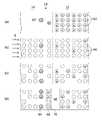
図1(a)-(d)は、半導体基板12と配線層14の界面18における導電層68の形成を模式的に示す図である。図1(a)は、イオン照射前の半導体基板12と配線層14の界面18の近傍の結晶状態を模式的に示す。半導体基板12は、例えばp型のシリコンであり、多数のキャリア(正孔)62が分布している。配線層14は、酸化シリコンなどの酸化物で構成される絶縁体層であり、界面18の近傍に固定電荷(正電荷)64が存在する。半導体基板12と配線層14の界面18は、半導体と絶縁体の接合により、空乏層60が形成される。空乏層60の厚さは、1μm以下であり、典型的には数nm~数十nm程度である。 1A to 1D are diagrams schematically showing formation of a
図1(b)は、イオンビームBの照射後の半導体基板12と配線層14の界面18の近傍の結晶状態を模式的に示す。イオン照射により、半導体基板12および配線層14には多数の格子欠陥66が形成される。図1(c)は、イオン照射後に250℃~300℃程度の加熱処理中の状態を模式的に示し、熱処理によって格子欠陥66が部分的に回復する様子を示している。半導体基板12の内部では、格子欠陥66の回復により欠陥数が減少し、キャリア(正孔)62が増加していく。また、配線層14の内部でも格子欠陥66の回復により欠陥数が減少し、界面18の近傍において固定電荷64の増加や界面準位への正孔62の捕獲が生じうる。その結果、熱処理後の図1(d)に示されるように、界面18において半導体基板12のアクセプタ準位の電子70が引き寄せられ、界面18の近傍の電子密度が増加し、界面18の近傍に導電層68が形成されうる。導電層68は、イオン照射前の半導体基板12(例えば1~10Ω・cm)よりも抵抗率の低い領域である。導電層68の抵抗率は、例えば1Ω・cm未満(例えば10-1Ω・cm以下または10-2Ω・cm以下)である。FIG. 1B schematically shows the crystal state near the
図1(d)に示す導電層68は、半導体基板12と配線層14の界面18の近傍に多数の格子欠陥66を形成した後に250℃~300℃程度の熱処理を加えることで生じると考えられる。現在の半導体装置の製造工程において、250℃~300℃程度の熱処理を加えないようにすることは難しい。そこで、本実施の形態では、半導体基板12と配線層14の界面18の近傍がp型半導体ではなく、n型半導体となるようにすることで、熱処理後の界面18に導電層68が形成されるのを防ぐようにする。 The
図2は、半導体基板12と配線層14の界面18の近傍をn型化した場合のエネルギーバンド図である。図2は、上述の図1(d)と同様、高抵抗領域を形成するためのイオン照射後に250℃~300℃程度の熱処理を加えた後の状態を示している。半導体基板12内の界面18に隣接する第1領域32は、n型化した領域(n-領域)であり、電子が多数キャリアとなっている。一方、半導体基板12内の第1領域32よりも深い第2領域34は、p型領域(p+領域)であり、正孔が多数キャリアとなっている。配線層14内の界面18の近傍には正の固定電荷64が存在するため、界面18における半導体基板12のバンドは障壁が高くなるように曲がっている。その結果、熱処理後に配線層14内の界面18の近傍の固定電荷64が増加した状態となっても、界面18における導電層68の形成を防止できる。FIG. 2 is an energy band diagram when the vicinity of the
本実施の形態では、p型半導体基板12の界面18の近傍をn型化する手法として、水素イオンを利用する。p型基板内に照射された水素イオンは、熱処理によって活性化してn型キャリアとなりうる。したがって、イオン照射前の半導体基板12のp型キャリア濃度よりも多くのn型キャリア濃度を実現できれば、導電型をp型からn型に変えることができる。一般に、低抵抗(1~10Ω・cm)のp型シリコン基板のp型キャリア濃度は、1.0×1015cm-3~1.0×1016cm-3であることから、これよりも多くのn型キャリア濃度が実現されるように水素イオンを照射すればよい。In the present embodiment, hydrogen ions are used as a method for converting the vicinity of the
図3は、熱処理による水素の活性化率を示すグラフであり、温度と活性化率の関係を示している。図示されるように、200℃~400℃の範囲は、水素の活性化率が低く、温度上昇による活性化率の増加も緩やかである。一方、400℃を超えると、温度上昇による活性化率の増加率が大きくなり、活性化率の値も10%を超える。したがって、温度上昇による活性化率の増加が緩やかな200℃~400℃の範囲の熱処理を用いることで、後工程における熱処理の温度に個体差が生じる場合であっても、n型キャリア濃度の制御が容易となる。 FIG. 3 is a graph showing the activation rate of hydrogen by heat treatment, showing the relationship between the temperature and the activation rate. As shown in the figure, the activation rate of hydrogen is low in the range of 200° C. to 400° C., and the increase in the activation rate with increasing temperature is moderate. On the other hand, when the temperature exceeds 400° C., the rate of increase in the activation rate due to temperature rise increases, and the value of the activation rate exceeds 10%. Therefore, by using heat treatment in the range of 200 ° C. to 400 ° C. where the activation rate increases slowly with temperature rise, even if there is an individual difference in the temperature of the heat treatment in the subsequent process, the n-type carrier concentration can be controlled. becomes easier.
図4は、熱処理によるキャリア濃度変化を模式的に示すグラフであり、異なる四つの水素密度について、熱処理によりドナー化されるn型キャリア濃度の値を模式的に示す。Aは水素密度が5×1016cm-3(0.5×1017cm-3)であり、Bは水素密度が1.0×1017cm-3であり、Cは水素密度が1.5×1017cm-3であり、Dは水素密度が2.0×1017cm-3である。グラフ中の破線は、半導体基板12の抵抗率2Ω・cm、4Ω・cmおよび10Ω・cmに対応するp型キャリア濃度を示している。FIG. 4 is a graph schematically showing changes in carrier concentration due to heat treatment, and schematically shows values of n-type carrier concentrations that are converted to donors by heat treatment for four different hydrogen densities. A has a hydrogen density of 5×1016 cm−3 (0.5×1017 cm−3 ), B has a hydrogen density of 1.0×1017 cm−3 , and C has a hydrogen density of 1.0×10 17 cm −3 . 5×1017 cm−3 and D has a hydrogen density of 2.0×1017 cm−3 . The dashed lines in the graph indicate p-type carrier concentrations corresponding to resistivities of the
例えば、水素イオンの照射後に250℃~300℃程度の熱処理を加えて水素イオンをドナー化する場合、基板抵抗率が4Ω・cmであれば1.0~1.5×1017cm-3程度の水素密度でn型反転化できることが分かる。同様に基板抵抗率が2Ω・cmであれば2.0×1017cm-3程度の水素密度でn型反転化できる。また、基板抵抗率が10Ω・cmであれば0.5×1017cm-3程度の水素密度でn型反転化できる。なお、n型反転化に必要となる条件は、半導体基板12の抵抗率に応じて水素密度および加熱温度の双方を調整することで適宜設定できる。For example, when heat treatment at about 250° C. to 300° C. is applied after hydrogen ion irradiation to convert the hydrogen ions into donors, if the substrate resistivity is 4 Ω·cm, then about 1.0 to 1.5×1017 cm−3 . It can be seen that n-type inversion can be achieved at a hydrogen density of . Similarly, if the substrate resistivity is 2 Ω·cm, n-type inversion can be achieved with a hydrogen density of about 2.0×1017 cm−3 . Also, if the substrate resistivity is 10 Ω·cm, n-type inversion can be achieved with a hydrogen density of about 0.5×1017 cm−3 . The conditions required for n-type inversion can be appropriately set by adjusting both the hydrogen density and the heating temperature according to the resistivity of the
図5は、水素イオン照射のドーズ量と水素密度の関係の一例を示すグラフであり、水素イオンの加速エネルギーを2MeV,4MeV,8MeV,17MeVとした場合について示す。図示されるように、水素イオンのドーズ量と照射後の水素密度は比例関係にある。また、照射エネルギーが低いほど得られる水素密度は高い。これは、加速エネルギーが低いと水素イオンが注入される深さ方向の範囲が限定され、単位体積あたりの水素注入量が増えるためである。グラフより、0.5~2.0×1017cm-3の水素密度を実現するためには、2MeVまたは4MeVであれば0.5~2.0×1014cm-2程度、8MeVであれば1.0~4.0×1014cm-2程度、17MeVであれば3.5×1014cm-2程度以上にすればよい。なお、これらのドーズ量でイオン照射をすれば、500Ω・cm以上の高抵抗率の実現に必要な1×1017cm-3以上の欠陥密度を得ることもできる。FIG. 5 is a graph showing an example of the relationship between the dose amount of hydrogen ion irradiation and the hydrogen density, and shows cases where the hydrogen ion acceleration energies are 2 MeV, 4 MeV, 8 MeV, and 17 MeV. As shown in the figure, the dose amount of hydrogen ions and the hydrogen density after irradiation are in a proportional relationship. Also, the lower the irradiation energy, the higher the hydrogen density obtained. This is because when the acceleration energy is low, the depth range in which hydrogen ions are implanted is limited, and the amount of hydrogen implanted per unit volume increases. From the graph, in order to achieve a hydrogen density of 0.5 to 2.0×1017 cm−3 , it is necessary to achieve a hydrogen density of 0.5 to 2.0×10 14 cm −2 for 2 MeV or 4 MeV, and 0.5 to 2.0×1014 cm−2 for 8 MeV. 1.0 to4.0.times.10.sup.14 cm.sup.-2 for example, and about3.5.times.10.sup.14 cm.sup.-2 or higher for 17 MeV. By ion irradiation with these doses, it is also possible to obtain a defect density of 1×1017 cm−3 or more, which is necessary for realizing a high resistivity of 500 Ω·cm or more.
以上の考察より、本実施の形態では、p型の半導体基板12と配線層14の界面18の近傍をn型化するための第1の水素イオン照射と、半導体基板12内に厚い高抵抗領域を形成するための第2の水素イオン照射とを組み合わせる手法を提案する。 From the above consideration, in the present embodiment, the first hydrogen ion irradiation for converting the vicinity of the
図6は、実施の形態に係る半導体装置10の構造を模式的に示す断面図である。半導体装置10は、システムLSIやシステム・オン・チップといった集積回路(IC)である。半導体装置10は、半導体基板12と、配線層14とを備える。 FIG. 6 is a cross-sectional view schematically showing the structure of the
本明細書において、半導体基板12と配線層14の界面18に直交する方向を上下方向または深さ方向ということがある。また、半導体基板12の内部において、界面18に向かう方向を上方向または上側、界面18と反対側の裏面20に向かう方向を下方向または下側ということがある。また、界面18に平行する方向を横方向または水平方向ということがある。 In this specification, the direction orthogonal to the
半導体基板12は、抵抗率が10Ω・cm以下の低抵抗の半導体基板であり、抵抗率が1~10Ω・cm程度の半導体基板である。半導体基板12は、例えば、チョクラルスキー(CZ)法により作製されたp型のシリコン(Si)ウェハであり、p型キャリア濃度が1015cm-3~1016cm-3程度である。CZ法により作製されたウェハは、フローティングゾーン(FZ)法等により作製された高抵抗ウェハと比較して抵抗率が低く、安価である。ある実施例において、半導体基板12の抵抗率は4Ω・cmであり、p型キャリア濃度が3.4×1015cm-3である。The
半導体基板12の上には配線層14が設けられる。配線層14は、多層配線構造を有し、例えば、複数の層間絶縁層と、層間絶縁層内に形成される配線部とを有する。配線層14の厚さt0は、5μm~30μm程度であり、例えば10μm、15μmまたは20μm程度である。配線層14に形成される配線部として、例えば、水平方向に延びる水平配線や、異なる層に形成される水平配線同士を接続するために上下方向に延びるビア配線などが設けられる。また、配線層14の表面16上にはインダクタ素子28が形成される。インダクタ素子28は、配線層14の表面16上でループ状または渦巻状に延びる帯状導電体により形成される。 A
半導体装置10は、半導体素子領域22とインダクタ素子領域24を有する。半導体素子領域22には、トランジスタやダイオードなどの半導体素子26が設けられる。半導体素子領域22の半導体基板12内には、半導体素子26を形成するためのウェル領域、ソース/ドレイン領域、コンタクト領域などの不純物拡散層が設けられる。インダクタ素子領域24には、配線層14に形成されるインダクタ素子28が設けられる。 The
インダクタ素子28の直下の半導体基板12の内部には、高抵抗領域30が設けられる。高抵抗領域30は、半導体基板12のボディ部分38よりも抵抗率が高い領域である。高抵抗領域30は、水素(H)を半導体装置10に照射することにより形成される。高抵抗領域30は、界面18の近傍の第1領域32と、第1領域32よりも深い位置の第2領域34とを有する。 A
第1領域32は、界面18と隣接する領域であり、n型反転化した領域である。第1領域32は、n型反転化のために高濃度の水素が注入されている領域とも言える。第1領域32の抵抗率は、100Ω・cm以上であり、好ましくは500Ω・cmまたは1kΩ・cm以上である。したがって、第1領域32は、導電型がn型であり、半導体基板12のボディ部分38より高抵抗率の「n型高抵抗領域」である。第1領域32の厚さt1は、できるだけ小さいことが望ましく、10μm以下または5μm以下であることが好ましい。第1領域32の厚さt1は、1μm~2μm程度であってもよい。 The
第2領域34は、第1領域32と深さ方向に連続する領域であり、p型が維持された領域である。第2領域34の抵抗率は、100Ω・cm以上であり、好ましくは500Ω・cm以上または1kΩ・cm以上である。したがって、第2領域34は、導電型がp型であり、半導体基板12のボディ部分38より高抵抗率の「p型高抵抗領域」である。第2領域34の厚さt2は、できるだけ大きいことが望ましく、20μm以上、50μm以上または100μm以上であることが好ましい。 The
つづいて、本実施の形態に係る半導体装置10の製造方法について述べる。図7は、半導体装置10の製造方法を模式的に示すフローチャートである。まず、p型の半導体基板12に半導体素子26を形成し(S10)、半導体基板12の上に配線層14を形成し、形成した素子や配線を保護するための保護膜を形成する(S14)。S10~S14の工程は、半導体プロセスにおいて「前工程」といわれる工程であり、熱酸化、熱拡散、CVD、アニールといった400℃以上の高温処理がなされうる。 Next, a method for manufacturing the
次に、半導体基板12にイオン照射して高抵抗領域30を形成し(S16)、半導体基板12の裏面研磨がなされる(S18)。S16およびS18の工程は、いわゆる「中間工程」または「ポストパッシベーションプロセス(PPP;Post Passivation Process)」といわれる工程である。 Next, the
その後、熱処理を含む後工程(S20)がなされ、半導体集積回路として完成する。S20の後工程では、例えば、ウェハをダイシングして個片化する工程、個片化されたチップを実装基板上に接着するダイボンド工程、実装基板とチップとをワイヤボンドで結線する工程、チップを樹脂で封止する工程などが含まれる。例えば、ダイボンド工程、ワイヤボンド工程および樹脂封止工程では、200℃~300℃程度の熱処理がなされ、ある実施例において熱処理の最高温度は260℃程度である。なお、ボンディングや封止工程とは別に半導体装置10を加熱するアニール処理がなされてもよい。このアニール処理は、高抵抗領域30を250℃以上300℃以下の所定温度で加熱することにより、高抵抗領域30の抵抗率を安定化させてもよい。このアニール処理は、10分以下の比較的短い時間実行すれば十分であり、5分以下、1分以下、または、30秒以下の時間であってもよい。 Thereafter, a post-process (S20) including heat treatment is performed to complete a semiconductor integrated circuit. In the post-process of S20, for example, a step of dicing the wafer into individual pieces, a die bonding step of adhering the separated chips onto a mounting substrate, a step of connecting the mounting substrate and the chips by wire bonding, and A step of sealing with resin and the like are included. For example, in the die bonding process, wire bonding process and resin sealing process, heat treatment is performed at about 200.degree. C. to 300.degree. Annealing treatment for heating the
つづいて、S16のイオン照射による高抵抗領域30の形成方法について詳述する。図8は、実施の形態に係る第1イオン照射工程を模式的に示す断面図であり、上述の第1領域32を形成する工程を示す。半導体装置10の上方には、インダクタ素子領域に対応する部分に開口42が設けらるマスク40が配置されている。第1の水素イオン照射では、マスク40を用いて配線層14の上から半導体装置10に向けてイオンビームB1を照射する。これにより、インダクタ素子28の直下の半導体基板12内に第1領域32が形成される。 Next, a method for forming the
第1の水素イオン照射では、半導体基板12と配線層14の界面18から第1深さd1の深さ位置(第1深さ位置ともいう)を狙って高ドーズ量のイオンビームB1が照射される。第1深さd1は10μm以内であり、例えば5μm以下である。第1深さd1は、第1領域32の厚さt1よりも小さい。界面18から少しだけ深い位置を狙って高ドーズ量のイオン照射することで、界面18の近傍に高濃度の水素イオンを照射することができ、熱処理後にn型反転化された第1領域32を形成できる。 In the first hydrogen ion irradiation, a high-dose ion beam B1 is irradiated from the
図9は、実施の形態に係る第2イオン照射工程を模式的に示す断面図であり、上述の第2領域34を形成する工程を示す。第2イオン照射では、第1イオン照射と共通のマスク40を用いて配線層14の上からイオンビームB2が照射される。第2イオン照射では、界面18から第2深さd2の深さ位置(第2深さ位置ともいう)を狙ってイオンビームB2が照射される。第2深さd2は、第1深さd1よりも大きく、界面18から20μm以上離れており、例えば30μm以上または50μm以上である。界面18から離れた深い位置を狙ってイオン照射することで、深さ方向に連続する厚い第2領域34を形成できる。 FIG. 9 is a cross-sectional view schematically showing the second ion irradiation step according to the embodiment, showing the step of forming the
第2イオン照射は、第2領域34の厚みt2が大きくなるように、第2深さd2の大きさを変化させて複数回実行されてもよい。例えば、界面18からの第2深さd2を50μmおよび90μmなどに設定することにより、深さ方向に100μm以上にわたって連続する高抵抗領域(第2領域34)を形成してもよい。第2イオン照射は、第1イオン照射の実行前になされてもよいし、第1イオン照射の実行後になされてもよい。 The second ion irradiation may be performed multiple times while changing the size of the second depth d2 such that the thickness t2 of the
第1イオン照射は、界面18の近傍のみに第1領域32を形成するため、基板内でイオンが到達する深さ方向の分布が相対的に小さいイオンビームを用いることが好ましいかもしれない。一方、第2イオン照射は、深さ方向に連続した厚い第2領域34を形成するため、基板内でイオンが到達する深さ方向の分布が相対的に大きいイオンビームを用いることが好ましいかもしれない。イオンが到達しうる深さ方向の分布は、例えばイオンビームのイオン種やエネルギーを変化させることで調整可能である。 Since the first ion irradiation forms the
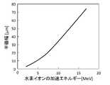
図10は、水素イオン照射のエネルギーと基板内でイオンが到達する深さ分布の半値幅の関係を示すグラフである。図示されるように、照射エネルギーが高いほど分布の半値幅が広くなることが分かる。界面18の近傍のn型反転化された第1領域32の厚さは10μm程度であれば十分であるため、2MeV以上5MeV以下のエネルギーの水素イオンを用いることで、界面18の近傍に高濃度の水素イオンを局所的に注入することができる。 FIG. 10 is a graph showing the relationship between the energy of hydrogen ion irradiation and the half width of the depth distribution reached by the ions in the substrate. As shown in the figure, the higher the irradiation energy, the wider the half width of the distribution. Since it is sufficient if the thickness of the n-type inverted
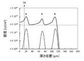
図11は、実施例に係るイオン照射後の半導体基板12内の欠陥密度分布および水素濃度分布を示すグラフであり、加熱処理前の分布を示している。グラフの深さ位置は、半導体基板12の表面16を基準としており、界面18が15μmの深さ位置に存在する。この実施例では、配線層14の上から水素イオンを複数回照射しており、20μm、70μmおよび110μmの3箇所の深さ位置にイオン照射している。イオン照射の深さ位置は、例えば、マスク40よりも手前に配置されるアブソーバの厚みを変えることで調整できる。20μmの深さ位置(界面18から5μmの深さ位置)は、第1の水素イオン照射に相当し、70μmおよび110μmの深さ位置(界面18から55μmおよび95μmの深さ位置)は第2の水素イオン照射に相当する。 FIG. 11 is a graph showing the defect density distribution and hydrogen concentration distribution in the
図11の実施例では、4MeVの水素イオン(1H+)を用いるとともに、照射位置の深さに応じてドーズ量を異ならせている。具体的には、20μmの深さ位置を2.0×1014cm-2のドーズ量とし、70μmの深さ位置を1.0×1014cm-2のドーズ量とし、110μmの深さ位置を2.0×1014cm-2のドーズ量としている。In the example of FIG. 11, 4 MeV hydrogen ions (1 H+ ) are used, and the dose is varied according to the depth of the irradiation position. Specifically, a dose of 2.0×1014 cm−2 is applied at a depth of 20 μm, a dose of 1.0×1014 cm−2 is applied at a depth of 70 μm, and a dose of 110 μm is applied. is a dose amount of 2.0×1014 cm−2 .
図11の実線は、欠陥密度分布を示す。図示されるように、0μmから120μmの深さ範囲にわたって欠陥密度が1×1018cm-3以上であるため、250℃~300℃程度の加熱処理後であっても500Ω・cm以上の高抵抗を実現できる。図11の破線は、水素密度を示す。図示されるように、界面18の近傍において0.5~3.0×1017cm-3の水素密度を実現することができており、250℃~300℃程度の熱処理後において界面18の近傍をn反転化させることができる。なお、300℃~400℃程度の熱処理を加えれば、より確実に界面18の近傍をn反転化させることができる。A solid line in FIG. 11 indicates the defect density distribution. As shown in the figure, since the defect density is 1×1018 cm−3 or more over the depth range of 0 μm to 120 μm, even after heat treatment at about 250° C. to 300° C., a high resistance of 500 Ω·cm or more is obtained. can be realized. The dashed line in FIG. 11 indicates the hydrogen density. As shown in the figure, a hydrogen density of 0.5 to 3.0×1017 cm−3 can be achieved in the vicinity of the
本実施例では、20μmの深さ位置(界面18から5μmの深さ位置)を狙った第1の水素イオン照射のドーズ量を大きくすることで、界面18の深さ位置における水素密度を高め、界面18の近傍を熱処理後にn反転化させることができる。さらに、70μmおよび110μmの深さ位置を狙った第2の水素イオン照射により、界面18から100μm程度の深さ範囲まで250℃~300℃程度の加熱処理後であっても500Ω・cm以上の程度の高抵抗を実現できる。したがって、本実施例によれば、導電層68の形成が抑制された好ましい高抵抗領域30を形成できる。 In this embodiment, the hydrogen density at the depth position of the
以上、本発明を実施の形態にもとづいて説明した。本発明は上記実施の形態に限定されず、種々の設計変更が可能であり、様々な変形例が可能であること、またそうした変形例も本発明の範囲にあることは、当業者に理解されるところである。 The present invention has been described above based on the embodiments. It should be understood by those skilled in the art that the present invention is not limited to the above embodiments, and that various design changes and modifications are possible, and that such modifications are within the scope of the present invention. It is about
上述の実施の形態では、イオン照射による高抵抗領域の形成(S16)の後に250℃~300℃程度の熱処理(S20)を施して水素をドナー化させる場合について示した。変形例においては、イオン照射中に半導体基板12を250℃~300℃に加熱してもよい。例えば、半導体基板12を保持するための保持装置に温度調整機構を設け、半導体基板12を加熱しながらイオン照射してもよい。また、ビーム照射により半導体基板12に与えられる熱エネルギーを利用して半導体基板12を250℃~300℃程度に加熱してもよい。この場合、半導体基板12を加熱または冷却しながらイオン照射することで、イオン照射中の基板温度が250℃~300℃程度に維持されるようにしてもよい。また、イオン照射中(S16)での熱処理と、後工程(S20)での熱処理が併用されてもよい。つまり、イオン照射中およびイオン照射後の少なくとも一方において半導体基板12を250℃~300℃程度の温度で加熱処理されてもよい。 In the above-described embodiment, the case where the heat treatment (S20) at about 250° C. to 300° C. is performed after the formation of the high-resistance region by ion irradiation (S16) is shown to convert hydrogen into a donor. In a modification, the
変形例においては、相対的に浅い位置の第1イオン照射後に300℃~400℃程度の熱処理(アニール処理)を実行することで、界面18の近傍をアニールして第1領域32に注入される水素イオンの活性化率を高めてもよい。その後、相対的に深い位置の第2イオン照射を実行し、深さ方向に厚い高抵抗領域を形成してもよい。 In the modified example, heat treatment (annealing) at about 300° C. to 400° C. is performed after irradiation of the first ions at a relatively shallow position, so that the vicinity of the
上述の実施の形態では、インダクタ素子28の直下に形成する高抵抗領域30について説明した。本実施の形態は、配線層14に形成されるアンテナ、伝送線路、キャパシタといった任意の受動素子の直下に形成される高抵抗領域に適用することも可能である。 In the above embodiments, the
10…半導体装置、12…半導体基板、14…配線層、16…表面、18…界面、20…裏面、30…高抵抗領域、32…第1領域、34…第2領域。 DESCRIPTION OF
Claims (8)
Translated fromJapanese前記イオン照射中および前記イオン照射後の少なくとも一方において前記半導体装置を250℃以上300℃以下の温度で加熱処理することと、を備え、
前記イオン照射は、
前記半導体基板と前記配線層の界面から10μm以内となる前記インダクタ素子の直下の前記半導体基板内の第1深さ位置に向けて、前記配線層の上から第1の水素イオン照射をすることと、
前記界面から20μm以上離れた前記インダクタ素子の直下の前記半導体基板内の第2深さ位置に向けて、前記配線層の上から第2の水素イオン照射をすることと、を含み、
前記第1の水素イオン照射および前記第2の水素イオン照射により、前記インダクタ素子の直下の前記半導体基板内において、前記界面の近傍に位置するn型高抵抗領域と、前記n型高抵抗領域よりも深くに位置し、前記n型高抵抗領域と深さ方向に連続するp型高抵抗領域とを含む前記高抵抗領域が形成されることを特徴とする半導体装置の製造方法。A semiconductor device comprising a p-type semiconductor substrate, a wiring layer formed on the surface of the semiconductor substrate,and an inductor element formed on the surface of the wiring layer is irradiated with ions to form the semiconductor devicedirectly below the inductor element. forming a high-resistance region having higher resistivity than before ion irradiation in a semiconductor substrate;
heat-treating the semiconductor device at a temperature of 250° C. or higher and 300° C. or lower during at least one of the ion irradiation and after the ion irradiation;
The ion irradiation is
A first hydrogen ion irradiation is performed from above the wiring layer toward a first depth position in the semiconductor substrateimmediately below the inductor element within 10 μm from the interface between the semiconductor substrate and the wiring layer. ,
irradiating a second hydrogen ion from above the wiring layer toward a second depth position in the semiconductor substrateimmediately below the inductor element at a distance of 20 μm or more from the interface;
By the first hydrogen ion irradiation and the second hydrogen ion irradiation, in the semiconductor substrate immediately below the inductor element, an n-type high-resistance region located near the interface and an n-type high-resistance region and forming the high-resistance region including the n-type high-resistance region and the p-type high-resistance region continuous in the depth direction .
前記第2の水素イオン照射は、前記第1深さ位置から前記第2深さ位置までの範囲の欠陥密度が8×1017cm-3以上となるようになされることを特徴とする請求項1に記載の半導体装置の製造方法。The first hydrogen ion irradiation is performed so that the hydrogen density at the first depth position is 5×1016 cm−3 or more,
3. The second hydrogen ion irradiation is performed so that the defect density in the range from the first depth position to the second depth position is 8×1017 cm−3 or more. 2. The method for manufacturing the semiconductor device according to 1.
前記半導体基板の表面に形成される配線層と、
前記配線層の表面上に形成されるインダクタ素子と、
前記半導体基板と前記配線層の界面から10μm以内となる前記インダクタ素子の直下の前記半導体基板内の第1深さ位置に設けられ、前記半導体基板よりも高抵抗率のn型高抵抗領域と、
前記界面から20μm以上離れた前記インダクタ素子の直下の前記半導体基板内の第2深さ位置に前記n型高抵抗領域と深さ方向に連続して設けられ、前記半導体基板よりも高抵抗率のp型高抵抗領域と、を備えることを特徴とする半導体装置。a p-type semiconductor substrate;
a wiring layer formed on the surface of the semiconductor substrate;
an inductor element formed on the surface of the wiring layer;
an n-type high-resistance region provided at a first depth position in the semiconductor substrateimmediately below the inductor element within 10 μm from the interface between the semiconductor substrate and the wiring layer and having a higher resistivity than the semiconductor substrate;
providedcontinuously in the depth direction with the n-type high-resistance region at a second depth position in the semiconductor substrateimmediately below the inductor element and separated from the interface by 20 μm or more, and having a resistivity higher than that of the semiconductor substrate; A semiconductor device comprising: a p-type high resistance region.
Priority Applications (2)
| Application Number | Priority Date | Filing Date | Title |
|---|---|---|---|
| JP2018242485AJP7169872B2 (en) | 2018-12-26 | 2018-12-26 | Semiconductor device and method for manufacturing semiconductor device |
| TW108133550ATWI727422B (en) | 2018-12-26 | 2019-09-18 | Semiconductor device and semiconductor device manufacturing method |
Applications Claiming Priority (1)
| Application Number | Priority Date | Filing Date | Title |
|---|---|---|---|
| JP2018242485AJP7169872B2 (en) | 2018-12-26 | 2018-12-26 | Semiconductor device and method for manufacturing semiconductor device |
Publications (2)
| Publication Number | Publication Date |
|---|---|
| JP2020107646A JP2020107646A (en) | 2020-07-09 |
| JP7169872B2true JP7169872B2 (en) | 2022-11-11 |
Family
ID=71449423
Family Applications (1)
| Application Number | Title | Priority Date | Filing Date |
|---|---|---|---|
| JP2018242485AActiveJP7169872B2 (en) | 2018-12-26 | 2018-12-26 | Semiconductor device and method for manufacturing semiconductor device |
Country Status (2)
| Country | Link |
|---|---|
| JP (1) | JP7169872B2 (en) |
| TW (1) | TWI727422B (en) |
Citations (6)
| Publication number | Priority date | Publication date | Assignee | Title |
|---|---|---|---|---|
| WO2003061009A1 (en) | 2002-01-16 | 2003-07-24 | Sanken Electric Co., Ltd. | Semiconductor device manufacturing method |
| JP2011049300A (en) | 2009-08-26 | 2011-03-10 | Toyota Motor Corp | Semiconductor device and method of manufacturing the same |
| JP2015119039A (en) | 2013-12-18 | 2015-06-25 | 住重試験検査株式会社 | Semiconductor device manufacturing method and semiconductor device |
| JP2017041598A (en) | 2015-08-21 | 2017-02-23 | 住重試験検査株式会社 | Semiconductor device and manufacturing method of the same |
| WO2017064949A1 (en) | 2015-10-16 | 2017-04-20 | 富士電機株式会社 | Semiconductor device and method for manufacturing semiconductor device |
| JP2018093184A (en) | 2016-12-02 | 2018-06-14 | 住重アテックス株式会社 | Semiconductor device and semiconductor device manufacturing method |
Family Cites Families (5)
| Publication number | Priority date | Publication date | Assignee | Title |
|---|---|---|---|---|
| JPS62169368A (en)* | 1985-09-10 | 1987-07-25 | Tdk Corp | Manufacture of vertical semiconductor device |
| US7851318B2 (en)* | 2007-11-01 | 2010-12-14 | Semiconductor Energy Laboratory Co., Ltd. | Semiconductor substrate and method for manufacturing the same, and method for manufacturing semiconductor device |
| CN105931967B (en)* | 2011-04-27 | 2019-05-03 | 株式会社半导体能源研究所 | Manufacturing method of semiconductor device |
| WO2013157183A1 (en)* | 2012-04-18 | 2013-10-24 | 住重試験検査株式会社 | Method for production of semiconductor device, and semiconductor device |
| TWI602293B (en)* | 2016-10-14 | 2017-10-11 | S H I Examination & Inspection Ltd | Semiconductor device and method of manufacturing semiconductor device |
- 2018
- 2018-12-26JPJP2018242485Apatent/JP7169872B2/enactiveActive
- 2019
- 2019-09-18TWTW108133550Apatent/TWI727422B/enactive
Patent Citations (6)
| Publication number | Priority date | Publication date | Assignee | Title |
|---|---|---|---|---|
| WO2003061009A1 (en) | 2002-01-16 | 2003-07-24 | Sanken Electric Co., Ltd. | Semiconductor device manufacturing method |
| JP2011049300A (en) | 2009-08-26 | 2011-03-10 | Toyota Motor Corp | Semiconductor device and method of manufacturing the same |
| JP2015119039A (en) | 2013-12-18 | 2015-06-25 | 住重試験検査株式会社 | Semiconductor device manufacturing method and semiconductor device |
| JP2017041598A (en) | 2015-08-21 | 2017-02-23 | 住重試験検査株式会社 | Semiconductor device and manufacturing method of the same |
| WO2017064949A1 (en) | 2015-10-16 | 2017-04-20 | 富士電機株式会社 | Semiconductor device and method for manufacturing semiconductor device |
| JP2018093184A (en) | 2016-12-02 | 2018-06-14 | 住重アテックス株式会社 | Semiconductor device and semiconductor device manufacturing method |
Also Published As
| Publication number | Publication date |
|---|---|
| JP2020107646A (en) | 2020-07-09 |
| TW202025387A (en) | 2020-07-01 |
| TWI727422B (en) | 2021-05-11 |
Similar Documents
| Publication | Publication Date | Title |
|---|---|---|
| JP6078961B2 (en) | Manufacturing method of semiconductor device | |
| KR100935567B1 (en) | Semiconductor device and method for manufacturing same | |
| US20080079119A1 (en) | Semiconductor device and method for manufacturing the same | |
| JP2017183419A (en) | Semiconductor device | |
| CN106062966A (en) | Semiconductor device and method for manufacturing semiconductor device | |
| TWI682520B (en) | Semiconductor device and method of manufacturing semiconductor device | |
| CN107068564A (en) | The method for forming semiconductor devices | |
| JP7125257B2 (en) | Semiconductor device and method for manufacturing semiconductor device | |
| JP6099553B2 (en) | Manufacturing method of semiconductor device | |
| JP6057534B2 (en) | Manufacturing method of semiconductor device | |
| US12426286B2 (en) | Radiation enhanced bipolar transistor | |
| JP7169872B2 (en) | Semiconductor device and method for manufacturing semiconductor device | |
| TWI717801B (en) | Manufacturing method of semiconductor device | |
| JP2008041836A (en) | Method of manufacturing semiconductor device | |
| JP7169871B2 (en) | Semiconductor device manufacturing method | |
| JP6557134B2 (en) | Semiconductor device and manufacturing method of semiconductor device | |
| US20170358649A1 (en) | Method of Manufacturing a Semiconductor Device Having an Impurity Concentration | |
| TW201227931A (en) | Semiconductor apparatus and manufacturing method thereof | |
| JP6385488B2 (en) | Manufacturing method of semiconductor device | |
| JP7537356B2 (en) | Manufacturing method of semiconductor epitaxial wafer |
Legal Events
| Date | Code | Title | Description |
|---|---|---|---|
| A625 | Written request for application examination (by other person) | Free format text:JAPANESE INTERMEDIATE CODE: A625 Effective date:20210917 | |
| A131 | Notification of reasons for refusal | Free format text:JAPANESE INTERMEDIATE CODE: A131 Effective date:20220726 | |
| A977 | Report on retrieval | Free format text:JAPANESE INTERMEDIATE CODE: A971007 Effective date:20220729 | |
| A521 | Request for written amendment filed | Free format text:JAPANESE INTERMEDIATE CODE: A523 Effective date:20220920 | |
| TRDD | Decision of grant or rejection written | ||
| A01 | Written decision to grant a patent or to grant a registration (utility model) | Free format text:JAPANESE INTERMEDIATE CODE: A01 Effective date:20221018 | |
| A61 | First payment of annual fees (during grant procedure) | Free format text:JAPANESE INTERMEDIATE CODE: A61 Effective date:20221031 | |
| R150 | Certificate of patent or registration of utility model | Ref document number:7169872 Country of ref document:JP Free format text:JAPANESE INTERMEDIATE CODE: R150 |