JP7169281B2 - Transmission lines, transmission lines with connectors, and repeaters - Google Patents
Transmission lines, transmission lines with connectors, and repeatersDownload PDFInfo
- Publication number
- JP7169281B2 JP7169281B2JP2019545642AJP2019545642AJP7169281B2JP 7169281 B2JP7169281 B2JP 7169281B2JP 2019545642 AJP2019545642 AJP 2019545642AJP 2019545642 AJP2019545642 AJP 2019545642AJP 7169281 B2JP7169281 B2JP 7169281B2
- Authority
- JP
- Japan
- Prior art keywords
- electric field
- field communication
- connector
- voltage
- insulator
- Prior art date
- Legal status (The legal status is an assumption and is not a legal conclusion. Google has not performed a legal analysis and makes no representation as to the accuracy of the status listed.)
- Active
Links
Images


Classifications
- H—ELECTRICITY
- H04—ELECTRIC COMMUNICATION TECHNIQUE
- H04B—TRANSMISSION
- H04B13/00—Transmission systems characterised by the medium used for transmission, not provided for in groups H04B3/00 - H04B11/00
- H—ELECTRICITY
- H04—ELECTRIC COMMUNICATION TECHNIQUE
- H04B—TRANSMISSION
- H04B3/00—Line transmission systems
- H04B3/54—Systems for transmission via power distribution lines
Landscapes
- Engineering & Computer Science (AREA)
- Computer Networks & Wireless Communication (AREA)
- Signal Processing (AREA)
- Power Engineering (AREA)
- Cable Transmission Systems, Equalization Of Radio And Reduction Of Echo (AREA)
- Testing Of Short-Circuits, Discontinuities, Leakage, Or Incorrect Line Connections (AREA)
Description
Translated fromJapanese本発明は、伝送線、コネクタ付き伝送線、及び中継器に関する。 The present invention relates to transmission lines, transmission lines with connectors, and repeaters.
一般に、制御信号の送受信や電力を供給するために電線やケーブルが種々の設備や装置に用いられている。例えば、特許文献1に記載の送電設備では、電力を送電するための送電線と、当該送電線の複数のポイントに設置された断線検出センサを中継装置と電気的に接続する信号電線路と、が用いられている。断線検出センサによって検出された送電線の断線情報が、当該信号電線路を通じて中継装置に送られている。このように、送電線とは別個に設けられた信号電線路などの信号線を用いることで、送電線に沿って信号を送る有線通信が可能となっている。 In general, wires and cables are used in various facilities and devices for transmitting and receiving control signals and for supplying power. For example, in the power transmission equipment described in
一方、電線やケーブルなどを使用しない通信技術として、電波を利用して信号の送受信を行う無線通信が知られている。このような無線通信は、電線などを必要としない反面、通信に用いられる電波がノイズとして他の装置や部品に影響するといった問題が生じ得る。 On the other hand, as a communication technology that does not use wires, cables, or the like, wireless communication that uses radio waves to transmit and receive signals is known. Although such wireless communication does not require electric wires or the like, there is a problem that radio waves used for communication affect other devices and parts as noise.
本願発明は、上記の課題に鑑み、電線やケーブルに沿って信号を送受信する場合に、当該信号の送受信に用いられる信号線を別途設ける必要がなく、かつ他の装置や部品に対する影響を低減することを目的とする。 In view of the above problems, the present invention eliminates the need to separately provide a signal line used for transmitting and receiving signals when transmitting and receiving signals along electric wires and cables, and reduces the influence on other devices and parts. for the purpose.
上記目的を達成するため、本願発明は、表面を形成する絶縁体、及び該絶縁体の内方に配された導線を含む伝送線であって、前記導線の第1端部と第2端部にそれぞれ配されて、前記絶縁体を通信媒体として電界通信を行う1対の電界通信モジュールと、前記電界通信モジュールの一方に接続され、前記電界通信により受信した情報又は該受信した情報の処理結果を出力する出力部と、を備える。 To achieve the above objects, the present invention provides a transmission line including an insulator forming a surface and a conductor disposed within the insulator, the conductor having a first end and a second end. and a pair of electric field communication modules that perform electric field communication using the insulator as a communication medium, and information received by the electric field communication or a processing result of the received information connected to one of the electric field communication modules. and an output unit that outputs the
また、前記第1端部の電圧を測定する第1測定部と、前記第2端部の電圧を測定する第2測定部と、前記第1端部の電圧と第2端部の電圧を取得して、該第1端部の電圧と該第2端部の電圧の電位差に基づいて前記導線の状態を判定する判定部と、を備え、前記判定部は、前記一対の電界通信モジュールによる電界通信により前記第2端部の電圧を取得する構成であってもよい。 Also, a first measuring unit that measures the voltage of the first end, a second measuring unit that measures the voltage of the second end, and obtains the voltage of the first end and the voltage of the second end and a determination unit that determines the state of the conductor based on the potential difference between the voltage at the first end and the voltage at the second end, wherein the determination unit detects the electric field generated by the pair of electric field communication modules. The voltage of the second end may be obtained through communication.
さらに、前記第1測定部は、前記第1端部から生じる特定の周波数帯域における信号を抽出する第1フィルタを有し、当該抽出した信号に基づいて前記第1端部の電圧を測定し、前記第2測定部は、前記第2端部から生じる特定の周波数帯域における信号を抽出する第2フィルタを有し、当該抽出した信号に基づいて前記第2端部の電圧を測定する構成であってもよい。 Further, the first measurement unit has a first filter that extracts a signal in a specific frequency band generated from the first end, measures the voltage of the first end based on the extracted signal, The second measuring unit has a second filter that extracts a signal in a specific frequency band generated from the second end, and measures the voltage of the second end based on the extracted signal. may
本発明のコネクタ付き伝送線は、上記の伝送線と、前記電界通信モジュールの一方および前記出力部を内蔵するコネクタと、を備える。 A transmission line with a connector according to the present invention includes the transmission line described above, and a connector incorporating one of the electric field communication modules and the output section.
本発明の中継器は、表面を形成する絶縁体を有する電線またはケーブルの第1端部に設けられたコネクタと機器が有するコネクタとを中継する中継器であって、前記第1端部の絶縁体に容量結合される電界通信モジュールを備え、前記電界通信モジュールは、前記絶縁体を通信媒体として、前記電線または前記ケーブルの第2端部側に設けられた電界通信モジュールと電界通信を行う。 A repeater of the present invention is a repeater that relays a connector provided at a first end of an electric wire or cable having an insulator forming a surface and a connector of a device, wherein the insulation of the first end is An electric field communication module capacitively coupled to a body is provided, and the electric field communication module performs electric field communication with the electric field communication module provided on the second end side of the electric wire or the cable using the insulator as a communication medium.
本発明の伝送線、コネクタ付き伝送線、及び中継器は、電界通信モジュール同士が絶縁体を通信媒体とする電界通信を行うことで、当該電界通信により受信した情報又は当該情報の処理結果を機器に対して出力することができる。このように電界通信モジュール同士による電界通信を用いて情報の送受信が可能となっているので、通信用の電線を別途設ける必要がない。また、電界通信に用いられる電力は微弱であるため、他の装置や部品に対する影響を低減させることが可能となっている。 The transmission line, the transmission line with a connector, and the repeater of the present invention perform electric field communication between electric field communication modules using an insulator as a communication medium, so that the information received by the electric field communication or the processing result of the information is transmitted to the device. can be output to Since information can be transmitted and received using electric field communication between electric field communication modules in this way, there is no need to separately provide a communication wire. In addition, since the electric power used for electric field communication is weak, it is possible to reduce the influence on other devices and parts.
[第1実施形態]
以下、図面に基づいて、本発明の実施形態に係るコネクタ付き伝送線を説明する。[First embodiment]
A transmission line with a connector according to an embodiment of the present invention will be described below with reference to the drawings.
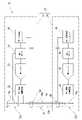
図1に示すように、本実施形態のコネクタ付き伝送線10は、主制御回路2から周辺回路4に対してDC電力を供給するものであり、電源ラインとして用いられる電線12およびグランドラインとして用いられる電線14を備えている。各電線12,14は、銅やアルミニウム合金などを主な原材料とする導体が線状に形成された単線や撚り線などの導線12a,14a(図2)と、導線12a,14aを覆う絶縁体12b,14b(図2)と、を備えている。 As shown in FIG. 1, the
コネクタ付き伝送線10は、両電線12,14の第1端部に配された第1コネクタ16と、両電線12,14の第2端部に配された第2コネクタ18と、を備えている。第1コネクタ16は、主制御回路2のコネクタ2aに接続され、第2コネクタ18は周辺回路4のコネクタ4aに接続される。第1コネクタ16および第2コネクタ18は、コネクタ2a,4aに嵌入されるハウジングを有しており、当該ハウジング内には各導線12a,14aと導通する接続端子(不図示)が設けられている。 The
本実施形態では、主制御回路2を内蔵する主制御機器(不図示)に対して反復動作する周辺機器(不図示)内に上記の周辺回路4が設けられており、当該反復動作による撓みや屈曲に起因する電線12,14の劣化状態を点検する点検装置20(図2)がコネクタ付き伝送線10に備えられている。なお、電線12,14の劣化状態とは、導線12a,14aの一部に亀裂等が生じ、導線12a,14aが断線しかかった状態のことである。 In the present embodiment, the
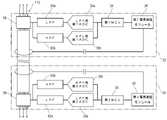
図2に示すように、点検装置20は、第1コネクタ16(図1)内に設けられた第1ユニット22と、第2コネクタ18(図1)内に設けられた第2ユニット24と、を備えている。 As shown in FIG. 2, the
第1ユニット22および第2ユニット24には、それぞれ差動増幅回路26,28、アナログ-デジタル変換器(以下、「ADC」という)30,32、マイクロコンピュータ(以下、「MCU」という)34,36、及び電界通信モジュール38,40などの電子デバイスが基板上に実装されている。これらの電子デバイスには、上記の電源ラインを入力電源とする定電圧回路(不図示)から一定の電源が供給されている。なお、以下の説明において、これらの電子デバイスをユニット22,24ごとに区別する場合には、第1ユニット22の電子デバイスをそれぞれ第1差動増幅回路26、第1ADC30、第1MCU34、及び第1電界通信モジュール38といい、第2ユニット24の電子デバイスをそれぞれ第2差動増幅回路28、第2ADC32、第2MCU36、及び第2電界通信モジュール40という。 The
第1差動増幅回路26は、入力の一方が導線12aの第1端部に接続され、入力の他方が導線14aの第1端部に接続されている。これら入力の電圧の差が第1差動増幅回路26から出力される。なお、当該出力が定電圧回路により供給される電源電圧よりも若干低いレベルとなるように増幅率が予め定められている。したがって、第1差動増幅回路26からは第1端部における導線12a,14a間の電圧を指標するアナログ信号が出力される。第2差動増幅回路28は、第1差動増幅回路26と同様の回路構成であり、第2端部における導線12a,14a間の電圧を指標するアナログ信号を出力する。各差動増幅回路26,28から出力された信号は、各差動増幅回路26,28に対応して接続されたADC30,32に入力される。各ADC30,32の出力はMCU34,36に接続されており、ADC30,32によって変換されたデジタル信号がMCU34,36へと入力される。 The first
各MCU34,36には、上記のADC30,32に加えて、電界通信モジュール38,40が接続されている。各電界通信モジュール38,40は、絶縁体12b,14bの表面に発生させた電界により信号を伝達する電界通信を行うモジュールであって、絶縁体12b,14bに巻きつけられた電極42,44を介して、第1端部および第2端部の絶縁体12b,14bに対して容量結合されている。このように電線12,14の表面を形成している絶縁体12b,14bは電界通信の通信媒体となっている。 Electric
ここで、本実施形態の第1MCU34は、メモリに格納されたプログラムがCPUに実行されることで、第1端部における導線12a,14a間の電圧を取得する。このような第1MCU34、並びに電極42、第1差動増幅回路26、及び第1ADC30は、電線12の第1端部における導線12a,14a間の電圧を測定する第1測定部46(図3)として機能する。同様に、第2MCU36は、メモリに格納されたプログラムがCPUに実行されることで、第2端部における導線12a,14a間の電圧を取得する。このような第2MCU、並びに電極44、第2差動増幅回路28、及び第2ADC32は、電線12の第2端部における導線12a,14a間の電圧を測定する第2測定部50(図3)として機能する。また、下記の動作フローで説明するように、第1MCU34は、第2MCU36から受信した電圧と測定した電圧の電位差に基づいて、導線12a,14aの劣化状態を判定する判定する判定部48(図3)として機能する。また、第1MCU34は判定結果を出力する出力部52(図3)として機能する。 Here, the
以下、第1ユニット22および第2ユニット24の動作フローを説明する。 The operation flow of the
図1に示すように、第1コネクタ16および第2コネクタ18がコネクタ2a,4aに接続された状態で主制御装置が起動されると、主制御回路2の電力が導線12aを介して定電圧回路に供給され、定電圧回路から電子デバイスへと電力が供給される。これにより各MCU34,36が起動して上記プログラムに定められた処理を開始する。 As shown in FIG. 1, when the main control unit is activated with the
図4に示すように、処理が開始されると、先ず、各MCU34,36は、タイミングを合わせて後述の測定処理(s102,s202)を実行するための同期処理(s101,s201)を実行する。具体的には、同期処理(s101)では、第1MCU34が第1電界通信モジュール38を制御して、同期の開始を指標するトリガーを第1電界通信モジュール38から第2電界通信モジュール40へと送信する。同期処理(s201)では、第2MCU36が、第2電界通信モジュール40を制御して、トリガーの受信状態を繰り返し確認する。そして、トリガーの受信を確認すると、第2MCU36は測定処理(s202)を実行する。第1MCU34はトリガーを送信した後に測定処理(s102)を実行する。 As shown in FIG. 4, when the process is started, the
測定処理(s102,s202)は、導線12a,14a間の電圧を測定する処理である。具体的には、測定処理(s102)では、第1MCU34が、第1ADC30を制御して、第1差動増幅回路26から入力されたアナログ信号をデジタル信号へと変換させる。そして、第1MCU34は、当該デジタル信号に基づいて、第1端部における導線12a,14a間の電圧を指標する電圧値(以下、「第1電圧値」という)を取得する。第2MCU36も同様に処理を実行(s202)し、第2端部における各導線12a,14a間の電圧を指標する電圧値(以下、「第2電圧値」)を取得する。 The measurement process (s102, s202) is a process of measuring the voltage between the
各MCU34,36は、測定処理を実行した後に通信処理(s103,s203)を実行する。具体的には、通信処理(s103)では、第1MCU34が第1電界通信モジュール38を制御して、第2電圧値の送信リクエストを第1電界通信モジュール38から第2電界通信モジュール40に対して送信する。通信処理(s203)では、第2MCU36が、第2電界通信モジュール40を制御して、送信リクエストの受信状況を確認する。そして、送信リクエストの受信を確認すると、第2MCU36は、第2電界通信モジュール40を制御して、測定処理(s202)において取得した第2電圧値を第1電界通信モジュール38へと送信する。第1MCU34は、第1電界通信モジュール38を制御して第2電圧値の有無を確認し、第2電圧値を受信すると判定処理を実行する。 Each
判定処理は、第1電圧値と第2電圧値に基づいて導線12a,14aの劣化状態を判定する処理であって、第1MCU34が、減算処理(s104)、第1比較処理(s105)、第2比較処理(s106)、及び信号出力処理(s107a、s107b)を順に実行する。 The determination process is a process of determining the state of deterioration of the
減算処理(s104)では、第1電圧値から第2電圧値が減じられて、第1端部と第2端部間の電位差が求められる。当該電位差は、導線12a,14aの劣化の進行による導体抵抗の増大に伴って値が増加する。すなわち、減算処理(s104)で求められる電位差は導線12a,14aの劣化状態を指標している。 In the subtraction process (s104), the second voltage value is subtracted from the first voltage value to obtain the potential difference between the first end and the second end. The potential difference increases as the conductor resistance increases due to the progress of deterioration of the
第1比較処理(s105)では、導線12a,14aの劣化が少ないと判断すべき電位差の上限値(第1閾値)と減算処理(s104)で求められた電位差が比較される。比較の結果、電位差が第1閾値よりも小さい場合には処理を終了する。一方、減算処理で求められた電位差が第1閾値よりも大きい場合には、第2比較処理(s106)が実行される。 In the first comparison process (s105), the upper limit value (first threshold value) of the potential difference at which deterioration of the
第2比較処理(s106)では、導線12a,14aの劣化が多いと判断すべき電位差の下限値(第2閾値)と減算処理(s104)で求められた電位差が比較される。比較の結果、減算処理で求められた電位差が第2閾値よりも小さい場合には、劣化が進行中であることを指標する警告信号を出力端子から出力する(s107a)。一方、減算処理で求められた電位差が第2閾値よりも大きい場合には、劣化が多いことを指標する劣化信号を出力端子から出力する(s107b)。これら警告信号と劣化信号は、第1コネクタ16を介して主制御装置に対して送信される。主制御機器は、警告信号または劣化信号を受信すると、その旨をユーザや管理者に対して通知する。 In the second comparison process (s106), the lower limit value (second threshold value) of the potential difference at which it should be determined that deterioration of the
このように点検装置20が上記処理を実行することで、導線12a,14aの劣化状態が点検される。なお、これらの処理は、主制御装置の起動時のみに限られず、主制御装置の運転中に定期的に実行されても構わない。 As the
本実施形態のコネクタ付き伝送線10によれば、電線12,14を交換する目安をユーザや管理者に知らせることができる。また、第1電界通信モジュール38と第2電界通信モジュール40を用いた電界通信を行うことで、通信用の電線(信号線)を別途設けることなく、両端部における電圧を同期しながら測定することができ、また、第2端部の電圧を第1端部において取得することが可能となっている。さらに、電界通信に用いられる電力は微弱であるため、主制御回路2や周辺回路4に対する影響を低減させることが可能となっている。また、電波環境の悪いところなど、電波を用いた無線通信では通信接続が担保できない恐れがあったが、本実施形態の伝送線10によれば、第1端部から第2端部にかけて設けられている絶縁体12b,14bを通信媒体とするため、電波環境の良し悪しに関わらず安定した通信接続を担保することができる。 According to the
以上、本発明に係るコネクタ付き伝送線10を実施形態に基づいて説明したが、本発明は上記した形態に限られないことは勿論であり、例えば、以下のような形態で実施されても構わない。 Although the
<変形例1>
上記の動作フローにおける同期処理は必須の処理ではなく、同期処理を省略したフローであっても構わない。<
Synchronization processing in the operation flow described above is not essential processing, and a flow in which synchronization processing is omitted may be used.
<変形例2>
上記実施形態の差動増幅回路26,28に変えて、電源ラインの電圧を分圧する分圧回路を用い、分圧回路の出力をADC30,32に入力しても構わない。<
Instead of the
<変形例3>
上記の動作フローでは第1比較処理(s105)と第2比較処理(s106)を実行していたが、第1比較処理(s105)のみを実行し、当該第1比較処理(s105)において、電位差が第1閾値よりも大きいと判断された場合に警告信号を出力しても構わない。<Modification 3>
Although the first comparison process (s105) and the second comparison process (s106) are executed in the above operation flow, only the first comparison process (s105) is executed, and in the first comparison process (s105), the potential difference A warning signal may be output when it is determined that is greater than the first threshold.
<変形例4>
また、上記実施形態では判定結果を主制御回路2へと出力していたが、第1コネクタ16に多色LEDの発光部を露出させて設け、当該多色LEDの発光によって判定結果をユーザや管理者に知らせても構わない。例えば、第2比較処理(s106)において、電位差が第2閾値よりも小さければ多色LEDを黄色に発光させ、電位差が第2閾値よりも大きければ多色LEDを赤色に発光させる。これにより、ユーザや管理者は劣化状態を直感的に知ることができる。<
In addition, in the above embodiment, the determination result is output to the
<変形例5>
上記実施形態のコネクタ付き伝送線10は、主制御回路2から周辺回路4へと電力を供給するための電源ラインとして用いられる電線12と、グランドラインとして用いられる電線14と、を備えているが、さらに主制御回路2が周辺回路4を制御するための制御ラインとして用いられる他の電線を備えてもよい。<Modification 5>
The transmission line with
上記他の電線をさらに備える態様においては、第1端部における導線14aと他の導線間の電圧を測定するための第3差動増幅回路が第1ユニット22に設けられ、第2端部における導線14aと他の導線間の電圧を測定するための第4差動増幅回路が第2ユニット24に設けられる。また、第1ユニット22のADCには、第1差動増幅回路26の出力信号と第3差動増幅回路の出力信号を切り換えてAD変換する多チャンネルのADCが用いられる。同様に、第2ユニット24のADCには、第2差動増幅回路28の出力信号と第4差動増幅回路の出力信号を切り換えてAD変換する多チャンネルのADCが用いられる。 In the embodiment further including the other electric wire, the
このような第1ユニット22では、測定処理(s102)がADCの各チャンネルに対して実行される。これにより、第1MCU34は、第1差動増幅回路26の出力に対応する第1電圧値と、第3差動増幅回路の出力に対応する第3電圧値と、を取得する。第2ユニット24では、測定処理(s202)がADCの各チャンネルに対して実行され、第2差動増幅回路28の出力に対応する第2電圧値と、第4差動増幅回路の出力に対応する第4電圧値と、が取得される。 In such a
そして、通信処理(s103,s203)において、電界通信により第2電圧値と第4電圧値が第1MCU34に送信される。また、第1MCU34による減算処理(s104)および比較処理(s105,s106)により、第1電圧値と第2電圧値の電位差に基づいて導線12aの劣化状態が判定され、第3電圧値と第4電圧値の電位差に基づいて他の導線の劣化状態が判定される。 Then, in the communication processing (s103, s203), the second voltage value and the fourth voltage value are transmitted to the
<変形例6>
本実施形態のコネクタ付き伝送線は、絶縁体であるシース64(図5)によって電線12,14が被覆された態様であっても構わない。すなわち、コネクタ付き伝送線はケーブルを備えても構わない。このような態様においては、シース64の第1端部および第2端部の各々に電極が巻きつけられ、各電極を介して電界通信モジュール38,40がシース64に対して容量結合される。そして、シース64の表面に発生させた電界により信号を伝達する電界通信が行われる。すなわち、ケーブルを備えるコネクタ付き伝送線は、シース64が電界通信の通信媒体となる。<Modification 6>
The transmission line with a connector of the present embodiment may have a mode in which the
<変形例7>
本実施形態に係るコネクタ付き伝送線は、図5に示されるように、電力用の電線12,14および信号線54から成る電線群112を一纏めにして劣化状態を判定しても構わない。当該態様においては、電線群112の各端部における絶縁体12b,14b,54bに巻きつけられる帯状電極56,58と、入力が当該帯状電極56,58に対して電気的に接続された第1フィルタ60および第2フィルタ62と、入力が各フィルタ60,62の出力に電気的に接続された第1ADC30および第2ADC32と、各ADC30,32を制御可能に電気的に接続された第1MCU34および第2MCU36と、が第1ユニット22および第2ユニット24に設けられている。<Modification 7>
As for the transmission line with a connector according to the present embodiment, as shown in FIG. 5, a
帯状電極56,58は、例えば導体である銅がテープ状に形成された銅箔テープであり、絶縁体12b,14b,54bに対する取付面に接着層が形成されている。この帯状電極56,58は絶縁体12b,14b,54bを束ねるように巻き付けられている。このように帯状電極56,58が巻き付けられていることにより、帯状電極56,58は電線群112からの電波を受ける。 The
ここで、本変形例において、周辺機器を稼働させる前に帯状電極56,58が受ける電波は図6(a)に示す通りである。一方、周辺機器を稼働させた場合に帯状電極56,58が受ける電波は図6(b)に示す通りである。各図を比較して分かるように、周辺機器を稼働させる前後において2kHz付近のスペクトラムに差異が生じており、周辺機器を稼働させた後には電圧が10dB程度増加することとなる。換言すれば、電線群112に劣化が生じると、電線群112の第2端部における当該増加分が減少する(停止させた状態の電圧に近づく)こととなり、本変形例では当該増加分の減少を検出することにより電線の劣化を検出しようとするものである。 Here, in this modified example, the radio waves received by the
したがって、第1ユニット22と第2ユニット24に設けられた両フィルタ60,62は、上記周波数成分の信号を取り出すように設定されており、同じ周波数帯域(通過帯域や阻止帯域)を有することが好ましい。なお、上記の通り本例における周辺機器では取り出すべき周波数成分は2kHzであるが、周辺機器に対して入力する信号や供給する電力の周波数に応じて当該取り出すべき周波数成分は適宜設定される。また、一般的に電力の周波数は信号の周波数に比べて低いことから、図7に示すように、電線群112における電力用の電線12,14から発せられる電波の周波数成分を取り出すためのローパスフィルタ(以下、LPF60a,62a)と、信号線54から発せられる電波の周波数成分を取り出すためのハイパスフィルタ(以下、HPF60b,62b)と、LPF60a,62aの出力信号をデジタル信号に変換するLPF用ADC30a,32aと、HPF60b,62bの出力信号をデジタル信号に変換するHPF用ADC30b,32bと、を設けて電線12,14と信号線54の劣化を区別して検出するよう構成しても構わない。 Therefore, both
図5に戻り、両フィルタ60,62から出力された信号は対応するADC30,32によってデジタル信号へと変換されて、MCU34,36へと入力され、MCU34,36によって電圧値が取得されることとなる。MCU34,36によって電圧値が取得されるまでのフローについては、上記の実施形態と同様に、同期処理(s101)が実行された上で測定処理(s102)により取得される。ここで、図7に示すように、LPF60a,62a(電線12,14用のフィルタ)とHPF60b,62b(信号線54用のフィルタ)を用いる場合には、LPF60a,62aにより取り出された信号から電圧を測定するための第1同期処理及び電力線測定処理が実行され、次いでHPF60b,62bにより取り出された信号から電圧を測定するための第2同期処理及び信号線測定処理が実行される。 Returning to FIG. 5, the signals output from both
また、通信処理(s103)では、電界通信を用いて、第2ユニット24から第1ユニット22に対して電圧値が送信されるが、2種類のフィルタ(LPF60a,62aおよびHPF60b,62b)が用いられる場合には、電力線測定処理において測定された電力線電圧値と、信号線測定処理において測定された信号線電圧値が送信される。そして、減算処理(s104)では、第1ユニット22の電力線電圧値から第2ユニット24の電力線電圧値が減じられで電力用の電線12,14の電位差が求められ、第1ユニット22の信号線電圧値から第2ユニット24の信号線電圧値が減じられ信号線54の電位差が求められる。 In the communication process (s103), the voltage value is transmitted from the
そして、第1比較処理(s105)では、上記の減算処理(s104)において求められた電線12,14の電位差と第1閾値との比較、及び信号線54の電位差と第1閾値との比較が実行される。なお、この第1閾値は電線12,14と信号線54のそれぞれに対して個別に設定されても構わない。比較の結果、いずれかの電位差が第1閾値より大きい場合には第2比較処理が実行される。第2比較処理では、電線12、14の電位差と第2閾値との比較、及び信号線54の電位差と第2閾値との比較が実行される。なお、第2閾値値は電線12,14と信号線54のそれぞれに対して個別に設定されても構わない。比較の結果、第1比較処理において大きいと判断された値が第2閾値よりも小さい場合には警告信号が出力される(s107a)。一方、第2閾値よりも大きい場合には劣化信号が出力される(s107b)。 Then, in the first comparison process (s105), the potential difference between the
本変形例に係るコネクタ付き伝送線によれば、電線群112単位で劣化の有無を判定することができる。従って、電線群112を構成する電線の本数に応じて回路の部品点数やMCUの処理数を増減させる必要がない。特に、多数の電線が複合した多芯ケーブルであっても同一の部品点数で構成できるので、ユニット22,24の肥大化を防止したり、製品コストの増大を抑制することができる。 According to the transmission line with a connector according to this modified example, it is possible to determine the presence or absence of deterioration for each
なお、特定の周波数帯域を効率的に取り出すために、上記のLPF60a,62aとHPF60b,62bの両方または一方をバンドパスフィルタに代えても構わない。また、当該バンドパスフィルタは、取り出すべき周波数帯域をMCU34,36によって適宜設定可能となるようにMCU34,36と電気的に接続されても構わない。このように周波数帯域を適宜設定するためには、周辺機器の稼働前において、全ての周波数帯域についてバンドパスフィルタから出力された電圧値を取得し、メモリに一旦記憶させておき、周辺機器の稼働後に、再度、全ての周波数についてバンドパスフィルタから出力された電圧値を取得する。そして、各周波数について、一旦記憶させておいた電圧値と再度取得した電圧値の各々を比較して差異が判別可能(又は顕著)な帯域をバンドパスフィルタより取り出すべき周波数帯域として設定することができる。 In order to efficiently extract a specific frequency band, both or one of the
<変形例8>
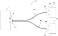
本実施形態に係るコネクタ付き伝送線は、図8に示されるように分岐型であっても構わない。当該コネクタ付き伝送線100は、主制御回路2から第1周辺回路104に配線される第1電線群112aと、主制御回路2から第2周辺回路114に配線される第2電線群112bと、を備えている。第1電線群112aと第2電線群112bの第1端部は共に共通のコネクタ(以下、「共通コネクタ」という。)116を介して主制御回路2のコネクタ2aに接続される。第1電線群112aの第2端部はコネクタ118aを介して第1周辺回路104のコネクタ104aに接続される。また、第2電線群112bの第2端部はコネクタ118bを介して第2周辺回路114のコネクタ114aに接続される。<Modification 8>
The transmission line with a connector according to this embodiment may be of a branched type as shown in FIG. The transmission line with
ここで、第1電線群112aのコネクタ118aには上記の第2ユニット24と同様のユニットが内蔵され、第2電線群112bのコネクタ118bにも上記の第2ユニット24と同様のユニットが内蔵される。 The
共通コネクタ116には、第1電線群112aにおける導線間の電圧を測定するための差動増幅回路と、第2電線群112bにおける導線間の電圧を測定するための差動増幅回路と、各差動増幅回路の出力信号をAD変換する多チャンネルのADCと、第1電線群112aおよび第2電線群112bに巻きつけられた電極を介して各電線群112a,112bに対して容量結合された電界通信モジュールと、MCUと、を備えるユニットが内蔵される。 The
共通コネクタ116内の電界通信モジュールは、第1電線群112aの絶縁体12b,14bを通信媒体としてコネクタ118a内の電界通信モジュールと通信を行い、コネクタ118a側における第1電線群112aの導線間の電圧を受信する。また、共通コネクタ116内の電界通信モジュールは、第2電線群112bの絶縁体12b,14bを通信媒体としてコネクタ118b内の電界通信モジュールと通信を行い、コネクタ118b側における第2電線群112bの導線間の電圧を受信する。 The electric field communication module in the
共通コネクタ116内のMCUは、電界通信モジュールが受信したコネクタ118a側の導線間の電圧を取得すると共に、ADCを制御して、共通コネクタ116側における第1電線群112aの導線間の電圧を取得する。そして、取得した2つの電圧の電位差に基づいて、第1電線群112aの劣化状態を判定する。 The MCU in the
さらに、共通コネクタ116内のMCUは、電界通信モジュールが受信したコネクタ118b側の導線間の電圧を取得すると共に、ADCを制御して、共通コネクタ116側における第2電線群112bの導体間の電圧を取得する。そして、取得した2つの電圧の電位差に基づいて、第2電線群112bの劣化状態を判定する。 Furthermore, the MCU in the
<変形例9>
第1コネクタ16および第2コネクタ18は必須の構成ではなく、導線12a,14aの第1端部を主制御回路2に直接接続しても構わない。又は、導線12a,14aの第2端部を周辺回路4に直接接続しても構わない。すなわち、いずれか一方のコネクタのみ(例えば第1コネクタ16のみ)を備える構成であればよい。このような態様においては、他方のユニット(例えば第2ユニット24)は、接続された機器(例えば周辺機器)に内蔵されることとなる。<Modification 9>
The
<変形例10>
また、上記の点検装置20に変えて通信装置を備えても構わない。通信装置は、第1MCU34および第1電界通信モジュール38を有する第1ユニット22と、第2MCU36および第2電界通信モジュール40を有する第2ユニット24と、を備える。第1MCU34は第1コネクタ16を介してコネクタ2aの制御用端子に接続され、第2MCU36は第2コネクタ18を介してコネクタ4aの制御端子に接続される。そして、第1MCU34は、制御端子から入力された制御命令を取得し、第1電界通信モジュール38を制御して、当該制御命令を第2電界通信モジュール40へと送信する。第2MCU36は、第2電界通信モジュール40から制御命令を取得し、当該制御命令をコネクタ4aの制御端子に対して出力する。このように、第1MCU34は、第1コネクタ16が接続される機器からの入力を取得する取得部として機能し、第2MCU36は、電界通信を介して受信した情報を第2コネクタ18が接続される機器に対して出力する出力部として機能する。<
Also, a communication device may be provided in place of the
[第2実施形態]
第2実施形態に係る伝送線は、第1コネクタ16および第2コネクタ18を備えていない点で第1実施形態と異なるが、その他の構成は第1実施形態と同一である。すなわち、本実施形態の伝送線は、絶縁体12bに被覆された導線12aと、絶縁体14bに被覆された導線14aと、導線12a,14aの第1端部に配された第1ユニット22と、導線12a,14aの第2端部に配された第2ユニット24と、を備えた構成となっており、導線12a,14aの両端部は主制御回路2と周辺回路4に直に接続されている。第1ユニット22および第2ユニット24の動作フローも図4に示された第1実施形態の動作フローと同一である。なお、本実施形態に係る伝送線に上記の各変形例を適用しても構わない。[Second embodiment]
The transmission line according to the second embodiment differs from the first embodiment in that it does not have the
[第3実施形態]
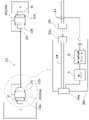
第3実施形態は、図9に示されるように、公知のコネクタ付き電線212と、一対の中継器300が用いられている点で第1実施形態とは異なっている。公知のコネクタ付き電線212は、導線12a,14a(図2)と、導線12a,14aを覆う絶縁体12b,14b(図2)と、導線12a,14aの両端部に設けられた一対のコネクタ216,218と、から構成されている。なお、当該コネクタ216,218には第1実施形態のユニット22,24は内蔵されていない。[Third embodiment]
The third embodiment, as shown in FIG. 9, differs from the first embodiment in that a known connector-equipped
一対の中継器300は、コネクタ付き電線212と主制御装置の間に配される第1中継器300aと、コネクタ付き電線212と周辺機器の間に配される第2中継器300bと、を備える。第1中継器300aは主制御装置とコネクタ付き電線212のコネクタ接続を中継し、第2中継器300bは周辺機器とコネクタ付き電線212のコネクタ接続を中継する。 The pair of
第1中継器300aは、コネクタ付き電線212の第1端部に設けられた第1コネクタ216に接続される電線側コネクタ302aと、主制御装置内の回路(主制御回路2)に設けられたコネクタ2aに接続される装置側コネクタ304aと、を備える。電線側コネクタ302aと装置側コネクタ304aの間には電路306が設けられており、当該電路306を介して、対応するコネクタ端子が導通している。 The
同様に、第2中継器300bは、コネクタ付き電線212の第2端部に設けられた第2コネクタ218に接続される電線側コネクタ302bと、周辺機器内の回路(周辺回路4)に設けられたコネクタ4aに接続される装置側コネクタ304bと、を備えており、対応するコネクタ端子を導通させる電路(不図示)が電線側コネクタ302bと装置側コネクタ304bの間に設けられている。 Similarly, the
ここで、一対の中継器300には、MCU34,36(図2)および電界通信モジュール38,40(図2)が内蔵されている。当該MCU34,36および電界通信モジュール38,40は、各中継器300a,300b内に設けられた電池(不図示)や主制御回路2から供給された電力により動作する。各電界通信モジュール38,40は、みの虫クリップなどの電極308を介して、コネクタ付き電線212の表面を形成する絶縁体12b,14b(図2)に容量結合されており、絶縁体12b,14bを通信媒体とした電界通信を行う。 Here, the pair of
第1MCU34は、装置側コネクタ304aを介して主制御回路2と通信可能に接続されており、周辺回路4に対する制御信号を主制御回路2から取得する。そして、第1MCU34は、制御信号を取得すると、第1電界通信モジュール38を制御して、当該制御信号を第2電界通信モジュール40へと送信する。 The
第2MCU36は、第2電界通信モジュール40を制御して制御信号を受信する。そして、第2MCU36は、制御信号を受信すると、装置側コネクタ304bを介して当該制御信号を周辺回路2に送信する。 The
本実施形態によると、主制御回路2から周辺回路4に対する制御信号が電界通信により送信されるので、制御信号を送信するための信号線を別途設ける必要がない。また、他の機器や部品に対する影響も低減することが可能である。さらに、本実施形態では公知のコネクタ付き電線212を用いることができるので、電界通信を行うための電線を新たに準備する必要がない。 According to this embodiment, since the control signal is transmitted from the
本実施形態では、公知のコネクタ付き電線212を例にして説明したが、公知のコネクタ付きケーブルを用いても構わない。当該コネクタ付きケーブルを用いる場合においては、一対の中継器200の電界通信モジュール38,40はケーブルのシース64に対して容量結合されることとなる。 In the present embodiment, a known cable with
また、本実施形態では、コネクタ付き電線212の端部の各々に中継器300a,300bを設けたが、例えば、周辺回路2内に電界通信モジュールを備える場合には、中継器300aのみであっても構わない。 Further, in the present embodiment, the
本発明は、その趣旨を逸脱しない範囲で当業者の知識に基づいて種々なる改良、修正、または変形を加えた態様でも実施できる。また、同一の作用又は効果が生じる範囲内で、何れかの発明特定事項を他の技術に置換した形態で実施しても良い。 The present invention can also be implemented in aspects with various improvements, modifications, or variations based on the knowledge of those skilled in the art without departing from the spirit of the invention. Moreover, any invention specifying matter may be replaced with another technique within the scope of producing the same action or effect.
10 伝送線
12,14 電線
12a,14a 導線
12b,14b 絶縁体
16 第1コネクタ
18 第2コネクタ
38 第1電界通信モジュール
40 第2電界通信モジュール
46 第1測定部
48 判定部
50 第2測定部
52 出力部
60 第1フィルタ
62 第2フィルタ
300 一対の中継器
300a 第1中継器
300b 第2中継器
REFERENCE SIGNS
Claims (5)
Translated fromJapanese前記導線の第1端部と第2端部にそれぞれ配されて、前記絶縁体を通信媒体として電界通信を行う1対の電界通信モジュールと、
前記第1端部および前記第2端部のそれぞれの前記絶縁体に巻き付けられる電極と、
前記電界通信モジュールの一方に接続され、前記電界通信により受信した情報又は該受信した情報の処理結果を出力する出力部と、を備え、
各電解通信モジュールは、対応する前記電極を介して前記第1端部または前記第2端部の絶縁体に対して容量結合されている伝送線。A transmission line comprising an insulator forming a surface and a conductor disposed within the insulator,
a pair of electric field communication modules arranged at the first end and the second end of the conducting wire and performing electric field communication using the insulator as a communication medium;
an electrode wrapped around the insulator at each of the first end and the second end;
an output unit connected to one of the electric field communication modules and outputting information received by the electric field communication or a processing result of the received information;
A transmission linein which each electrolytic communication module is capacitively coupled through the corresponding electrode to an insulator at the first end or the second end .
前記導線の第1端部と第2端部にそれぞれ配されて、前記絶縁体を通信媒体として電界通信を行う1対の電界通信モジュールと、
前記電界通信モジュールの一方に接続され、前記電界通信により受信した情報又は該受信した情報の処理結果を出力する出力部と、
前記第1端部の電圧を測定する第1測定部と、
前記第2端部の電圧を測定する第2測定部と、
前記第1端部の電圧と第2端部の電圧を取得して、該第1端部の電圧と該第2端部の電圧の電位差に基づいて前記導線の状態を判定する判定部と、を備え、
前記判定部は、前記一対の電界通信モジュールによる電界通信により前記第2端部の電圧を取得する伝送線。A transmission line comprising an insulator forming a surface and a conductor disposed within the insulator,
a pair of electric field communication modules arranged at the first end and the second end of the conducting wire and performing electric field communication using the insulator as a communication medium;
an output unit connected to one of the electric field communication modules and configured to output information received by the electric field communication or a processing result of the received information;
a first measuring unit that measures the voltage of the first end;
a second measuring unit that measures the voltage of the second end;
a determination unit that acquires the voltage of the first end and the voltage of the second end and determines the state of the conductor based on the potential difference between the voltage of the first end and the voltage of the second end;with
The determination unit is a transmission line that acquires the voltage of the second end by electric field communication by the pair of electric field communication modules .
前記第2測定部は、前記第2端部から生じる特定の周波数帯域における信号を抽出する第2フィルタを有し、当該抽出した信号に基づいて前記第2端部の電圧を測定する、
ことを特徴とする請求項2に記載の伝送線。The first measurement unit has a first filter that extracts a signal in a specific frequency band generated from the first end, measures the voltage of the first end based on the extracted signal,
The second measurement unit has a second filter that extracts a signal in a specific frequency band generated from the second end, and measures the voltage of the second end based on the extracted signal.
3. The transmission line of claim 2, wherein:
前記電界通信モジュールの一方および前記出力部を内蔵するコネクタと、
を備えるコネクタ付き伝送線。A transmission line according to any one of claims 1 to 3;
a connector incorporating one of the electric field communication modules and the output unit;
A transmission line with a connector.
前記第1端部の絶縁体に容量結合される電界通信モジュールを備え、
前記電界通信モジュールは、前記絶縁体を通信媒体として、前記電線または前記ケーブルの第2端部側に設けられた電界通信モジュールと電界通信を行うことを特徴とする中継器。A repeater that relays a connector provided at a first end of an electric wire or cable having an insulator forming a surface and a connector of a device,
an electric field communication module capacitively coupled to the insulator at the first end;
The repeater, wherein the electric field communication module performs electric field communication with an electric field communication module provided on the second end side of the electric wire or the cable using the insulator as a communication medium.
Applications Claiming Priority (3)
| Application Number | Priority Date | Filing Date | Title |
|---|---|---|---|
| JP2017191958 | 2017-09-29 | ||
| JP2017191958 | 2017-09-29 | ||
| PCT/JP2018/036084WO2019065903A1 (en) | 2017-09-29 | 2018-09-27 | Transmission wire, connector-attached transmission wire, and relay |
Publications (2)
| Publication Number | Publication Date |
|---|---|
| JPWO2019065903A1 JPWO2019065903A1 (en) | 2020-11-05 |
| JP7169281B2true JP7169281B2 (en) | 2022-11-10 |
Family
ID=65902475
Family Applications (1)
| Application Number | Title | Priority Date | Filing Date |
|---|---|---|---|
| JP2019545642AActiveJP7169281B2 (en) | 2017-09-29 | 2018-09-27 | Transmission lines, transmission lines with connectors, and repeaters |
Country Status (3)
| Country | Link |
|---|---|
| JP (1) | JP7169281B2 (en) |
| CN (1) | CN111149307B (en) |
| WO (1) | WO2019065903A1 (en) |
Citations (3)
| Publication number | Priority date | Publication date | Assignee | Title |
|---|---|---|---|---|
| JP2008099235A (en) | 2006-09-11 | 2008-04-24 | Sony Corp | Communication system and communication apparatus |
| JP2008099234A (en) | 2006-09-11 | 2008-04-24 | Sony Corp | Communication system |
| JP2017505557A (en) | 2013-11-06 | 2017-02-16 | エイ・ティ・アンド・ティ インテレクチュアル プロパティ アイ,エル.ピー. | Millimeter wave surface wave communication |
Family Cites Families (5)
| Publication number | Priority date | Publication date | Assignee | Title |
|---|---|---|---|---|
| US5712875A (en)* | 1995-06-07 | 1998-01-27 | Compaq Computer Corporation | Asynchronous differential communication |
| JP4480735B2 (en)* | 2007-03-22 | 2010-06-16 | 日本電信電話株式会社 | Electric field communication device |
| JP5287423B2 (en)* | 2009-03-30 | 2013-09-11 | ソニー株式会社 | Communication device and high frequency coupler |
| US9768833B2 (en)* | 2014-09-15 | 2017-09-19 | At&T Intellectual Property I, L.P. | Method and apparatus for sensing a condition in a transmission medium of electromagnetic waves |
| JP2016092774A (en)* | 2014-11-11 | 2016-05-23 | 日立金属株式会社 | Communication monitoring system |
- 2018
- 2018-09-27JPJP2019545642Apatent/JP7169281B2/enactiveActive
- 2018-09-27WOPCT/JP2018/036084patent/WO2019065903A1/ennot_activeCeased
- 2018-09-27CNCN201880061994.4Apatent/CN111149307B/enactiveActive
Patent Citations (3)
| Publication number | Priority date | Publication date | Assignee | Title |
|---|---|---|---|---|
| JP2008099235A (en) | 2006-09-11 | 2008-04-24 | Sony Corp | Communication system and communication apparatus |
| JP2008099234A (en) | 2006-09-11 | 2008-04-24 | Sony Corp | Communication system |
| JP2017505557A (en) | 2013-11-06 | 2017-02-16 | エイ・ティ・アンド・ティ インテレクチュアル プロパティ アイ,エル.ピー. | Millimeter wave surface wave communication |
Also Published As
| Publication number | Publication date |
|---|---|
| CN111149307A (en) | 2020-05-12 |
| CN111149307B (en) | 2022-07-08 |
| WO2019065903A1 (en) | 2019-04-04 |
| JPWO2019065903A1 (en) | 2020-11-05 |
Similar Documents
| Publication | Publication Date | Title |
|---|---|---|
| EP3477316B1 (en) | Method of testing cable shield performance | |
| EP2642306B1 (en) | High voltage testing device | |
| US10962607B2 (en) | Method for testing multicore cable, method for manufacturing multicore cable assembly, and multicore cable test device | |
| KR101646964B1 (en) | Circuit apparatus and method for recognition earphone in electronic device | |
| ATE552771T1 (en) | TEST PLUG AND CABLE FOR GLUCOSE MONITORING DEVICE | |
| CN103399251B (en) | USB communication line detection device | |
| US9146268B2 (en) | Method and device for monitoring a sheath voltage arrester of a cable system | |
| KR101704861B1 (en) | Slip ring and slip ring electrical system | |
| US11009560B2 (en) | Method for testing multicore cable, method for manufacturing multicore cable assembly, and multicore cable test device | |
| TW201020563A (en) | Cable length detection and signal compensation apparatus and method | |
| CN112285577B (en) | Detection device | |
| JP7169281B2 (en) | Transmission lines, transmission lines with connectors, and repeaters | |
| KR101158540B1 (en) | Wide-band ultrasonic scanner for diagnosis of electrical facilities | |
| KR100777383B1 (en) | Detachable automatic detection earphone | |
| JP6974194B2 (en) | Bus-side connector, device-side connector and reading system | |
| JP5488891B2 (en) | Cable connection confirmation device | |
| KR101358047B1 (en) | Apparatus for learning and determining failure of electrical equipment using neural networks and ultrasonic signal | |
| JP2012193975A (en) | Electric apparatus insulation diagnostic device | |
| KR20180097298A (en) | System and method for monitoring electric wiring | |
| KR20140031672A (en) | Portable diagnostic device of live-line polymer insulators | |
| JP2000346901A (en) | Device for detecting partial discharge of electric apparatus and detector therefor | |
| WO2005027160A3 (en) | Arrangement for monitoring electric devices on stray light arcs | |
| JP2001228196A (en) | Partial discharge measurement method | |
| CN202929137U (en) | Antenna state detection circuit for ship automatic identification system terminal | |
| JP2013113691A (en) | Insulation diagnosis apparatus |
Legal Events
| Date | Code | Title | Description |
|---|---|---|---|
| RD02 | Notification of acceptance of power of attorney | Free format text:JAPANESE INTERMEDIATE CODE: A7422 Effective date:20200622 | |
| RD04 | Notification of resignation of power of attorney | Free format text:JAPANESE INTERMEDIATE CODE: A7424 Effective date:20200624 | |
| A521 | Request for written amendment filed | Free format text:JAPANESE INTERMEDIATE CODE: A523 Effective date:20200704 | |
| A621 | Written request for application examination | Free format text:JAPANESE INTERMEDIATE CODE: A621 Effective date:20210623 | |
| A131 | Notification of reasons for refusal | Free format text:JAPANESE INTERMEDIATE CODE: A131 Effective date:20220722 | |
| A521 | Request for written amendment filed | Free format text:JAPANESE INTERMEDIATE CODE: A523 Effective date:20220817 | |
| TRDD | Decision of grant or rejection written | ||
| A01 | Written decision to grant a patent or to grant a registration (utility model) | Free format text:JAPANESE INTERMEDIATE CODE: A01 Effective date:20221007 | |
| A61 | First payment of annual fees (during grant procedure) | Free format text:JAPANESE INTERMEDIATE CODE: A61 Effective date:20221028 | |
| R150 | Certificate of patent or registration of utility model | Ref document number:7169281 Country of ref document:JP Free format text:JAPANESE INTERMEDIATE CODE: R150 |