JP7166874B2 - Optical module mounting board and container mounting board - Google Patents
Optical module mounting board and container mounting boardDownload PDFInfo
- Publication number
- JP7166874B2 JP7166874B2JP2018201062AJP2018201062AJP7166874B2JP 7166874 B2JP7166874 B2JP 7166874B2JP 2018201062 AJP2018201062 AJP 2018201062AJP 2018201062 AJP2018201062 AJP 2018201062AJP 7166874 B2JP7166874 B2JP 7166874B2
- Authority
- JP
- Japan
- Prior art keywords
- lead pins
- optical module
- container
- optical
- lead
- Prior art date
- Legal status (The legal status is an assumption and is not a legal conclusion. Google has not performed a legal analysis and makes no representation as to the accuracy of the status listed.)
- Active
Links
Images

Classifications
- H—ELECTRICITY
- H10—SEMICONDUCTOR DEVICES; ELECTRIC SOLID-STATE DEVICES NOT OTHERWISE PROVIDED FOR
- H10F—INORGANIC SEMICONDUCTOR DEVICES SENSITIVE TO INFRARED RADIATION, LIGHT, ELECTROMAGNETIC RADIATION OF SHORTER WAVELENGTH OR CORPUSCULAR RADIATION
- H10F77/00—Constructional details of devices covered by this subclass
- H10F77/50—Encapsulations or containers
- H—ELECTRICITY
- H01—ELECTRIC ELEMENTS
- H01S—DEVICES USING THE PROCESS OF LIGHT AMPLIFICATION BY STIMULATED EMISSION OF RADIATION [LASER] TO AMPLIFY OR GENERATE LIGHT; DEVICES USING STIMULATED EMISSION OF ELECTROMAGNETIC RADIATION IN WAVE RANGES OTHER THAN OPTICAL
- H01S5/00—Semiconductor lasers
- H01S5/02—Structural details or components not essential to laser action
- H01S5/022—Mountings; Housings
- H01S5/0239—Combinations of electrical or optical elements
- H—ELECTRICITY
- H10—SEMICONDUCTOR DEVICES; ELECTRIC SOLID-STATE DEVICES NOT OTHERWISE PROVIDED FOR
- H10F—INORGANIC SEMICONDUCTOR DEVICES SENSITIVE TO INFRARED RADIATION, LIGHT, ELECTROMAGNETIC RADIATION OF SHORTER WAVELENGTH OR CORPUSCULAR RADIATION
- H10F77/00—Constructional details of devices covered by this subclass
- H10F77/40—Optical elements or arrangements
- H—ELECTRICITY
- H10—SEMICONDUCTOR DEVICES; ELECTRIC SOLID-STATE DEVICES NOT OTHERWISE PROVIDED FOR
- H10F—INORGANIC SEMICONDUCTOR DEVICES SENSITIVE TO INFRARED RADIATION, LIGHT, ELECTROMAGNETIC RADIATION OF SHORTER WAVELENGTH OR CORPUSCULAR RADIATION
- H10F77/00—Constructional details of devices covered by this subclass
- H10F77/93—Interconnections
- H10F77/933—Interconnections for devices having potential barriers
- H—ELECTRICITY
- H01—ELECTRIC ELEMENTS
- H01S—DEVICES USING THE PROCESS OF LIGHT AMPLIFICATION BY STIMULATED EMISSION OF RADIATION [LASER] TO AMPLIFY OR GENERATE LIGHT; DEVICES USING STIMULATED EMISSION OF ELECTROMAGNETIC RADIATION IN WAVE RANGES OTHER THAN OPTICAL
- H01S5/00—Semiconductor lasers
- H01S5/02—Structural details or components not essential to laser action
- H01S5/022—Mountings; Housings
- H01S5/02208—Mountings; Housings characterised by the shape of the housings
- H01S5/02216—Butterfly-type, i.e. with electrode pins extending horizontally from the housings
Landscapes
- Physics & Mathematics (AREA)
- Condensed Matter Physics & Semiconductors (AREA)
- General Physics & Mathematics (AREA)
- Electromagnetism (AREA)
- Optics & Photonics (AREA)
- Semiconductor Lasers (AREA)
- Light Receiving Elements (AREA)
- Geometry (AREA)
Description
Translated fromJapanese本発明は、光モジュール、光モジュール実装基板および容器に関する。 The present invention relates to an optical module, an optical module mounting substrate and a container.
光通信等に使用される光モジュールは、半導体レーザ素子等の複数の光学素子が容器内に収容された構成を有する(例えば特許文献1~4参照)。容器には、内部の光学素子を外部の制御器等と電気的に接続するためのリードピンが多数設けられている。このような光モジュールは、電気基板に実装されて用いられる。通常、リードピンは容器の実装面に垂直な面に、実装面と平行な面を形成するように一列に並べられて延びている。ここで、実装面とは、光モジュールが電気基板に実装されたときに電気基板と対向する面であり、通常は光モジュールの容器の底面である。そのため、実装の際は、各リードピンは先端側が実装面側に折り曲げられ、電気基板に形成された配線パターン等に半田等で固定される。 2. Description of the Related Art An optical module used for optical communication or the like has a structure in which a plurality of optical elements such as semiconductor laser elements are housed in a container (see
光通信の大容量化に伴って、光モジュールの小型化が強く要求されている。光モジュールを小型化するには、容器も小型化する必要がある。小型化した容器に所望の数のリードピンを設けるには、リードピンの間隔(ピッチ)を、従来と比較して狭くしなければならない場合がある。しかしながら、容器の小型化がさらに進むと、所望の数のリードピンを設けることが困難になるおそれがある。 As the capacity of optical communication increases, there is a strong demand for miniaturization of optical modules. In order to miniaturize the optical module, it is also necessary to miniaturize the container. In order to provide a desired number of lead pins in a miniaturized container, it may be necessary to narrow the interval (pitch) between the lead pins compared to the conventional case. However, if the size of the container is further reduced, it may become difficult to provide the desired number of lead pins.
この問題を解消するために、リードピンを実装面に垂直な方向(高さ方向)に二段に設けることが考えられる。しかしながら、リードピンを高さ方向に二段に設けた場合、光モジュールを電気基板に実装するために各リードピンを実装面側に折り曲げた際に、リードピン同士が干渉するおそれがある。 In order to solve this problem, it is conceivable to provide two stages of lead pins in a direction (height direction) perpendicular to the mounting surface. However, when the lead pins are provided in two stages in the height direction, the lead pins may interfere with each other when the lead pins are bent toward the mounting surface in order to mount the optical module on the electric board.
本発明は、上記に鑑みてなされたものであって、その目的は、リードピンの間のピッチを狭くでき、かつ電気基板への実装も容易である光モジュール、およびそのような光モジュールを実装した光モジュール実装基板、ならびに容器を提供することにある。 The present invention has been made in view of the above, and its object is to provide an optical module that can narrow the pitch between lead pins and that can be easily mounted on an electric substrate, and to mount such an optical module. An object of the present invention is to provide an optical module mounting substrate and a container.
上述した課題を解決し、目的を達成するために、本発明の一態様に係る光モジュールは、少なくとも1つの光素子と、前記少なくとも1つの光素子を収容する容器本体と、前記容器本体の側壁部に設けられた複数のリードピンと、を備え、前記複数のリードピンの少なくとも1つは前記少なくとも1つの光素子と電気的に接続しており、前記複数のリードピンは、前記側壁部の高さ方向において並ぶ複数の列を成し、かつ、上面視で隣接するリードピン同士が重ならない配置とされていることを特徴とする。 To solve the above-described problems and achieve the object, an optical module according to an aspect of the present invention includes at least one optical element, a container body that houses the at least one optical element, and a side wall of the container body. and a plurality of lead pins provided on the side wall portion, wherein at least one of the plurality of lead pins is electrically connected to the at least one optical element, and the plurality of lead pins extend in the height direction of the side wall portion. and lead pins adjacent to each other in a top view are arranged so as not to overlap each other.
本発明の一態様に係る光モジュールは、前記少なくとも1つの光素子は、半導体レーザ素子、半導体光増幅器、光変調器、受光素子のうちのいずれか1つもしくは複数の同種または異種の光素子であることを特徴とする。 In the optical module according to an aspect of the present invention, the at least one optical element is one or more of the same or different types of optical elements selected from a semiconductor laser element, a semiconductor optical amplifier, an optical modulator, and a light receiving element. characterized by being
本発明の一態様に係る光モジュールは、前記複数のリードピンは、上面視で0.7mm以下のピッチで並んでいることを特徴とする。 An optical module according to an aspect of the present invention is characterized in that the plurality of lead pins are arranged at a pitch of 0.7 mm or less when viewed from above.
本発明の一態様に係る光モジュールは、前記複数のリードピンは、前記側壁部の一面のみに設けられていることを特徴とする。 An optical module according to an aspect of the present invention is characterized in that the plurality of lead pins are provided only on one surface of the side wall portion.
本発明の一態様に係る光モジュールは、前記リードピンの先端側は、前記容器の高さ方向に向いており、かつ先端が略直線状に配列していることを特徴とする。 An optical module according to an aspect of the present invention is characterized in that the tip side of the lead pins faces the height direction of the container and the tips are arranged in a substantially straight line.
本発明の一態様に係る光モジュール実装基板は、前記光モジュールと、前記光モジュールが実装された電気基板と、を備えることを特徴とする。 An optical module mounting board according to an aspect of the present invention includes the optical module and an electric board on which the optical module is mounted.
本発明の一態様に係る容器は、容器本体と、前記容器本体の側壁部に設けられた複数のリードピンと、を備え、前記複数のリードピンは、前記側壁部の高さ方向において並ぶ複数の列を成し、かつ、上面視で隣接するリードピン同士が重ならない配置とされていることを特徴とする。 A container according to an aspect of the present invention includes a container body and a plurality of lead pins provided on a side wall portion of the container body, wherein the plurality of lead pins are arranged in a plurality of rows in a height direction of the side wall portion. and the lead pins adjacent to each other in a top view are arranged so as not to overlap each other.
本発明の一態様に係る容器は、前記リードピンの先端側は、前記容器の高さ方向に向いており、かつ先端が略直線状に配列していることを特徴とする。 A container according to an aspect of the present invention is characterized in that the tip ends of the lead pins face the height direction of the container, and the tips are arranged in a substantially straight line.
本発明によれば、リードピンの間のピッチを狭くでき、かつ電気基板への実装も容易であるという効果を奏する。 ADVANTAGE OF THE INVENTION According to this invention, the pitch between lead pins can be narrowed, and the mounting to an electric board is also easy.
以下、添付図面を参照しながら、本発明の実施形態を詳細に説明する。なお、以下に説明する実施形態により本発明が限定されるものではない。また、図面の記載において、同一または対応する要素には適宜同一の符号を付し、重複説明を適宜省略する。また、図面は模式的なものであり、各要素の寸法の関係、各要素の比率等は、現実と異なる場合があることに留意する必要がある。さらに、図面の相互間においても、互いの寸法の関係や比率が異なる部分が含まれている場合がある。 Hereinafter, embodiments of the present invention will be described in detail with reference to the accompanying drawings. In addition, this invention is not limited by embodiment described below. In addition, in the description of the drawings, the same or corresponding elements are denoted by the same reference numerals as appropriate, and overlapping descriptions are omitted as appropriate. Also, it should be noted that the drawings are schematic, and the relation of dimensions of each element, the ratio of each element, etc. may differ from reality. Furthermore, even between the drawings, there are cases where portions having different dimensional relationships and ratios are included.
(実施形態1)
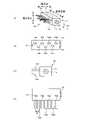
図1は、実施形態1に係る光モジュールの概略構成を示す模式図である。図1において、方向を示すために、互いに直交する長手方向、幅方向および高さ方向を規定する。図1(a)は光モジュール10の斜視図であり、図1(b)は光モジュール10を幅方向左側から見た図であり、図1(c)は光モジュール10を長手方向前側から見た図であり、図1(d)は光モジュール10を高さ方向上側から見た上面視の図である。(Embodiment 1)
FIG. 1 is a schematic diagram showing a schematic configuration of an optical module according to
光モジュール10は、容器1と、光素子2とを備えている。容器1は、底板部1aと、側壁部1bと、上蓋部1cと、光ポート1dと、複数のリードピン1eとを備えている。底板部1aは、長手方向および幅方向に広がる板状の部材である。側壁部1bは、高さ方向と、長手方向または幅方向に広がる4面を有する枠板状の部材であり、各面は底板部1aと略直交している。上蓋部1cは、底板部1aと対向して長手方向および幅方向に広がる板状の部材である。光ポート1dは、側壁部1bの長手方向前側に設けられている。光ポート1dは、外部に光を出力するまたは外部から光が入力されるためのポートであり、光の入力または出力のための光ファイバが接続される。 The
底板部1aは、たとえば銅タングステン(CuW)、銅モリブデン(CuMo)、酸化アルミニウム(Al2O3)、窒化アルミニウム(AlN)、銅(Cu)などの熱伝導率が高い材料からなる。上蓋部1c、光ポート1dは、たとえばFe-Ni-Co合金、酸化アルミニウム(Al2O3)、窒化アルミニウム(AlN)などの熱膨張係数が低い材料からなる。側壁部1bも主に上述したような熱膨張係数が低い材料からなるが、その幅方向左側の一部領域は、絶縁性の材質からなる配線領域が設けられている。配線領域には、導体からなる配線パターンが、容器1の内部と外部との間に延びるように形成されている。
側壁部1bの配線領域には、たとえばFe-Ni-Co合金、銅(Cu)などの導体からなる複数のリードピン1eが設けられている。リードピン1eの表面には、ハンダ付け性などのために、ニッケル(Ni)や金(Au)やそれらの多層めっきを施してもよい。本実施形態におけるリードピン1eの数は7本である。リードピン1eについては後に詳述する。 A plurality of
光素子2は、底板部1aと、側壁部1bと、上蓋部1cとが構成する容器本体1fに収容されている。光素子2は、電力や電気信号等を供給されて動作する光素子である。光素子2は、たとえば半導体レーザ素子、半導体光増幅器、光変調器、受光素子である。なお、本実施形態では1つの光素子2が収容されているが、光素子2の数は少なくとも1つであればよく、複数の光素子2が収容されていてもよい。複数の光素子2は同種の光素子でもよいし、互いに異種の光素子でもよい。光素子2は、ボンディングワイヤと配線領域の配線パターンとを介し、さらに7本のリードピン1eのうちの少なくとも一つを介して、光モジュール10の外部に設けられ制御器に電気的に接続されている。制御器は光モジュール10の動作、主には光素子2の動作を制御するものであり、たとえばIC(Integrated Circuit)を含んで構成されている。 The
7本のリードピン1eは、側壁部1bの高さ方向において並ぶ複数の列(本実施形態では2列)を成すように配置されている。本実施形態では、7本のリードピン1eのうち、4本のリードピン1eaが長手方向に一列をなすように配置されており、3本のリードピン1ebが、4本のリードピン1eaの高さ方向下側において、長手方向に一列をなすように配置されている。 The seven
このように、7本のリードピン1eが2列を成すように配置されていることにより、図1(d)に示すように上面視における隣接するリードピン1ea、1ebの間のピッチPを狭くできる。具体的には、ピッチPは、同じ列における隣接するリードピン1ea同士、リードピン1eb同士のピッチよりも狭くでき、たとえば0.7mm以下とできる。同じ列における隣接するリードピン1ea同士、リードピン1eb同士のピッチは、リードピンを設けるため必要なスペースや組立公差、リードピンの製造公差などによって制約を受けるが、本実施形態においてはその制約よりも狭いピッチPを実現できる。 By arranging the seven
本実施形態では、さらに、7本のリードピン1eは、図1(d)に示すように、上面視で隣接するリードピン同士が重ならない配置とされている。このような7本のリードピン1eは、いわゆる千鳥配置となっている。その結果、各リードピン1eの先端側を容器1の底面側に折り曲げられても、リードピン1e同士が干渉しない。 Further, in this embodiment, the seven
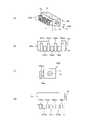
図2は、光モジュール10の各リードピン1eを折り曲げた状態のものである、光モジュール10Aを示す模式図である。図2(a)は光モジュール10Aの斜視図であり、図2(b)は光モジュール10Aを幅方向左側から見た図であり、図2(c)は光モジュール10Aを長手方向前側から見た図であり、図2(d)は光モジュール10Aを高さ方向上側から見た上面視の図である。光モジュール10Aは、容器1Aが折り曲げられた7本のリードピン1Aeを有する点で、光モジュール10と異なる。光モジュール10Aでは、各リードピン1Aeの先端側は、容器1Aの高さ方向の底面側に向いており、かつ先端が、リードピン1Aeが設けられた側壁部1bに略平行な直線Lに沿って、略直線状に配列している。具体的には、直線Lに沿って、リードピン1Aeaの先端とリードピン1Aebの先端とが交互に並んでいる。 FIG. 2 is a schematic diagram showing the
これにより、リードピンの先端が2列に並んでいる場合と比較して、光モジュール10Aを電気基板に容易に実装でき、かつ実装した場合に、電気基板上でのリードピン1Aeの実装面積を小さくできる。これによって、電気基板上におけるリードピン1Aeの実装密度を高めることができるとともに、光モジュール10A全体としての実装面積を小さくできる。 As a result, the
図3は、実施形態2に係る光モジュール実装基板の概略構成を示す模式図である。この光モジュール実装基板100は、光モジュール10Aと、光モジュール10Aが実装される電気基板20とを備えるものである。電気基板20には、光モジュール10Aの他に、電気デバイス21、22、23、24を含む複数の電気デバイスが実装されている。また、電気基板20には、これら複数の電子デバイスと光モジュール10Aとを電気的に接続するための配線パターンが設けられている。電気デバイス21、22、23、24は、光モジュール10Aが備える光素子の動作を制御する制御器を構成している。この制御器は、図示しない上位装置とコネクタピン等を介して電気的に接続されている。この制御器は、たとえば上位装置から指令信号を受信し、その指令に基づいて、光モジュール10Aの動作、主には光素子2の動作を制御する。 FIG. 3 is a schematic diagram showing a schematic configuration of an optical module mounting board according to the second embodiment. This optical
この光モジュール実装基板100は、上述したように電気基板20上での光モジュール10Aのリードピン1Aeの実装面積を小さくできる。その結果、リードピン1Aeの実装密度を高めることができるとともに、光モジュール10A全体としての実装面積を小さくできるので、フットプリントがより小さい電気基板20を実現できる。 This optical
なお、上記実施形態では、光モジュール10Aは、光モジュール10の各リードピン1eを折り曲げて作製したものであるが、折り曲げによらず、リードピン1Aeの形状を金型などを用いて成型して、光モジュール10Aを作製してもよい。 In the above embodiment, the
(他の実施形態)
図4(a)、(b)は、それぞれ、実施形態3、4に係る光モジュールの概略構成を示す模式図である。(Other embodiments)
FIGS. 4A and 4B are schematic diagrams showing schematic configurations of optical modules according to Embodiments 3 and 4, respectively.
図4(a)に示す光モジュール10Bは、図1に示す光モジュール10の構成において、容器1を容器1Bに置き換えた構成を有する。容器1Bは、容器1の構成において、各リードピン1eをリードピン1Beに置き換えた構成を有する。 An
7本のリードピン1Beは、千鳥配置とされている。具体的には、7本のリードピン1Beは、側壁部1bの高さ方向において並ぶ2列を成すように配置されている。7本のリードピン1Beのうち、4本のリードピン1Beaが長手方向に一列をなすように配置されており、3本のリードピン1Bebが、4本のリードピン1Beaの高さ方向下側において、長手方向に一列をなすように配置されている。また、7本のリードピン1Beは、上面視で隣接するリードピン同士が重ならない配置とされている。さらに、各リードピン1Beの先端側は、容器1Bの高さ方向(図の上下方向)の底面側に向いており、かつ先端が、リードピン1Beが設けられた側壁部1bに略平行な直線Lに沿って、略直線状に配列している。 The seven lead pins 1Be are staggered. Specifically, the seven lead pins 1Be are arranged in two rows in the height direction of the
これにより、上面視における隣接するリードピン1Bea、1Bebの間のピッチを、たとえば0.7mm以下と狭くできる。また、光モジュール10Bを電気基板に容易に実装でき、かつ実装した場合に、電気基板上でのリードピン1Beの実装面積を小さくでき、リードピンの実装密度を高めることができるとともに、光モジュール10B全体としての実装面積を小さくできる。 As a result, the pitch between adjacent lead pins 1Bea and 1Beb in top view can be narrowed to, for example, 0.7 mm or less. In addition, the
図4(b)に示す光モジュール10Cは、図1に示す光モジュール10の構成において、容器1を容器1Cに置き換えた構成を有する。容器1Cは、容器1の構成において、各リードピン1eをリードピン1Ceに置き換えた構成を有する。 An
7本のリードピン1Ceは、千鳥配置とされている。具体的には、7本のリードピン1Ceは、側壁部1bの高さ方向において並ぶ2列を成すように配置されている。7本のリードピン1Ceのうち、4本のリードピン1Ceaが長手方向に一列をなすように配置されており、3本のリードピン1Cebが、4本のリードピン1Ceaの高さ方向下側において、長手方向に一列をなすように配置されている。また、7本のリードピン1Ceは、上面視で隣接するリードピン同士が重ならない配置とされている。また、各リードピン1Ceの先端側は、容器1Cの高さ方向(図の上下方向)の底面側に向いており、かつ先端が、リードピン1Ceが設けられた側壁部1bに略平行な直線Lに沿って、略直線状に配列している。 The seven lead pins 1Ce are staggered. Specifically, the seven lead pins 1Ce are arranged in two rows in the height direction of the
これにより、上面視における隣接するリードピン1Cea、1Cebの間のピッチを、たとえば0.7mm以下と狭くできる。また、光モジュール10Cを電気基板に容易に実装でき、かつ実装した場合に、電気基板上でのリードピン1Ceの実装面積を小さくでき、リードピンの実装密度を高めることができるとともに、光モジュール10C全体としての実装面積を小さくできる。 As a result, the pitch between adjacent lead pins 1Cea and 1Ceb in top view can be narrowed to, for example, 0.7 mm or less. In addition, the
なお、上記各実施形態に係る光モジュール、たとえば光モジュール10は、各リードピン1eが側壁部1bの幅方向左側の一面のみに設けられている。このような構成は、電気基板上に、光モジュール10と、光モジュール10と対を成す他の光モジュールとを一緒に実装するのに適する。たとえば、光モジュール10が光送信モジュールである場合、他のモジュールは光受信モジュールである。また、他の光モジュールを、幅方向において光モジュール10と鏡面対称になるように構成すれば、光モジュール10と他の光モジュールとを、容器本体同士を近接させて実装することができる。 In the optical module according to each of the embodiments described above, for example, the
また、上記実施形態では、リードピンは、側壁部の高さ方向において2列を成すように配置されているが、3列以上を成すように配置されていてもよい。 Further, in the above embodiment, the lead pins are arranged in two rows in the height direction of the side wall, but they may be arranged in three or more rows.
また、上記実施形態では、リードピンの先端側は、容器の高さ方向の底面側を向いている。その理由は、上記実施形態に係る光モジュールが基板等に実装される際に、底面側が基板等に対向するからである。しかしながら、光モジュールが基板等に実装される際に、上面側が基板等に対向する際には、リードピンの先端側は、容器の高さ方向の上面側を向いていることが好ましい。すなわち、リードピンの先端側は、容器の高さ方向に向いており、その実装態様に応じて、底面側または上面側を向いていることが好ましい。 Further, in the above embodiment, the tip side of the lead pin faces the bottom side of the container in the height direction. The reason is that when the optical module according to the above embodiment is mounted on a substrate or the like, the bottom side faces the substrate or the like. However, when the optical module is mounted on a substrate or the like and the upper surface side faces the substrate or the like, it is preferable that the tip side of the lead pin faces the upper surface side in the height direction of the container. That is, the tip side of the lead pin faces the height direction of the container, and preferably faces the bottom side or the top side depending on the mounting mode.
また、上記実施形態により本発明が限定されるものではない。上述した各実施形態の構成要素を適宜組み合わせて構成したものも本発明に含まれる。また、さらなる効果や変形例は、当業者によって容易に導き出すことができる。よって、本発明のより広範な態様は、上記の実施形態に限定されるものではなく、様々な変更が可能である。 Moreover, the present invention is not limited by the above embodiments. The present invention also includes a configuration obtained by appropriately combining the constituent elements of the above-described embodiments. Further effects and modifications can be easily derived by those skilled in the art. Therefore, broader aspects of the present invention are not limited to the above-described embodiments, and various modifications are possible.
1、1A、1B、1C 容器
1a 底板部
1b 側壁部
1c 上蓋部
1d 光ポート
1e、1ea、1eb、1Ae、1Aea、1Aeb、1Be、1Bea、1Beb、1Ce、1Cea、1Ceb リードピン
1f 容器本体
2 光素子
10、10A、10B、10C 光モジュール
20 電気基板
21、22、23、24 電気デバイス
100 光モジュール実装基板
P ピッチ1, 1A, 1B,
Claims (5)
Translated fromJapanese前記光モジュールが実装された電気基板と、
を備え、
前記光モジュールは、
少なくとも1つの光素子と、
前記少なくとも1つの光素子を収容する容器本体と、
前記容器本体の側壁部に設けられた複数のリードピンと、
を備え、
前記複数のリードピンの少なくとも1つは前記少なくとも1つの光素子と電気的に接続しており、
前記複数のリードピンは、前記側壁部の高さ方向において並ぶ複数の列を成し、かつ、上面視で隣接するリードピン同士が重ならない配置とされており、
前記リードピンの先端側は、前記容器の高さ方向に向いており、かつ先端が略直線状に配列しており、
前記リードピン同士が重ならない配置であり、かつ前記リードピンの先端が略直線状に配列していることによって、前記リードピンの先端が実装面積を小さくして前記電気基板に実装されている
ことを特徴とする光モジュール実装基板。an optical module;
an electric board on which the optical module is mounted;
with
The optical module is
at least one optical element;
a container body that houses the at least one optical element;
a plurality of lead pins provided on the side wall of the container body;
with
at least one of the plurality of lead pins is electrically connected to the at least one optical element;
The plurality of lead pins form a plurality of rows aligned in the height direction of the side wall portion, and are arranged such that adjacent lead pins do not overlap each other when viewed from above,
The tip side of the lead pin faces the height direction of the container, and the tips are arranged in a substantially straight line,
By arranging the lead pins so that they do not overlap each other and by arranging the tips of the lead pins in a substantially straight line, the tips of the lead pins are mounted on the electric board with a small mounting area.
An optical modulemounting board characterized by:
前記容器が実装された電気基板と、
を備え、
前記容器は、
容器本体と、
前記容器本体の側壁部に設けられた複数のリードピンと、
を備え、
前記複数のリードピンは、前記側壁部の高さ方向において並ぶ複数の列を成し、かつ、上面視で隣接するリードピン同士が重ならない配置とされており、
前記リードピンの先端側は、前記容器の高さ方向に向いており、かつ先端が略直線状に配列しており、
前記リードピン同士が重ならない配置であり、かつ前記リードピンの先端が略直線状に配列していることによって、前記リードピンの先端が実装面積を小さくして前記電気基板に実装されている
ことを特徴とする容器実装基板。a container;
an electric substrate on which the container is mounted;
with
The container is
a container body;
a plurality of lead pins provided on the side wall of the container body;
with
The plurality of lead pins form a plurality of rows aligned in the height direction of the side wall portion, and are arranged such that adjacent lead pins do not overlap each other when viewed from above,
The tip side of the lead pin faces the height direction of the container, and the tips are arranged in a substantially straight line,
By arranging the lead pins so that they do not overlap each other and by arranging the tips of the lead pins in a substantially straight line, the tips of the lead pins are mounted on the electric board with a small mounting area.
A containermounting board characterized by:
Priority Applications (4)
| Application Number | Priority Date | Filing Date | Title |
|---|---|---|---|
| JP2018201062AJP7166874B2 (en) | 2018-10-25 | 2018-10-25 | Optical module mounting board and container mounting board |
| PCT/JP2019/042037WO2020085509A1 (en) | 2018-10-25 | 2019-10-25 | Optical module, optical module mounting substrate, and container |
| CN201980063071.7ACN112789721B (en) | 2018-10-25 | 2019-10-25 | Optical module, optical module mounting substrate and container |
| US17/228,913US20210234331A1 (en) | 2018-10-25 | 2021-04-13 | Optical module, optical module implemented substrate, and housing |
Applications Claiming Priority (1)
| Application Number | Priority Date | Filing Date | Title |
|---|---|---|---|
| JP2018201062AJP7166874B2 (en) | 2018-10-25 | 2018-10-25 | Optical module mounting board and container mounting board |
Publications (2)
| Publication Number | Publication Date |
|---|---|
| JP2020068332A JP2020068332A (en) | 2020-04-30 |
| JP7166874B2true JP7166874B2 (en) | 2022-11-08 |
Family
ID=70332025
Family Applications (1)
| Application Number | Title | Priority Date | Filing Date |
|---|---|---|---|
| JP2018201062AActiveJP7166874B2 (en) | 2018-10-25 | 2018-10-25 | Optical module mounting board and container mounting board |
Country Status (4)
| Country | Link |
|---|---|
| US (1) | US20210234331A1 (en) |
| JP (1) | JP7166874B2 (en) |
| CN (1) | CN112789721B (en) |
| WO (1) | WO2020085509A1 (en) |
Families Citing this family (1)
| Publication number | Priority date | Publication date | Assignee | Title |
|---|---|---|---|---|
| CN222015869U (en)* | 2024-03-14 | 2024-11-15 | 成都新易盛通信技术股份有限公司 | Nano-iTLA based on distributed feedback laser array |
Citations (6)
| Publication number | Priority date | Publication date | Assignee | Title |
|---|---|---|---|---|
| JP2003318419A (en) | 2002-04-24 | 2003-11-07 | Sumitomo Electric Ind Ltd | Optical communication module and its connection structure |
| JP2009004460A (en) | 2007-06-19 | 2009-01-08 | Opnext Japan Inc | Optical communication module and forming method of wiring pattern |
| JP2012047823A (en) | 2010-08-24 | 2012-03-08 | Opnext Japan Inc | Optical module and high frequency module |
| US20150155428A1 (en) | 2011-06-02 | 2015-06-04 | Electronics And Telecommunications Research Institute | Superluminescent diode, method of manufacturing the same, and wavelength-tunable external cavity laser including the same |
| JP2015169798A (en) | 2014-03-07 | 2015-09-28 | 富士通オプティカルコンポーネンツ株式会社 | Optical module |
| JP2015170729A (en) | 2014-03-07 | 2015-09-28 | 富士通オプティカルコンポーネンツ株式会社 | Optical module |
Family Cites Families (30)
| Publication number | Priority date | Publication date | Assignee | Title |
|---|---|---|---|---|
| US4734042A (en)* | 1987-02-09 | 1988-03-29 | Augat Inc. | Multi row high density connector |
| US5138438A (en)* | 1987-06-24 | 1992-08-11 | Akita Electronics Co. Ltd. | Lead connections means for stacked tab packaged IC chips |
| JPH0732042B2 (en)* | 1990-10-11 | 1995-04-10 | 富士通株式会社 | Through-hole connection type electronic device and its mounting method |
| GB9216327D0 (en)* | 1991-09-10 | 1992-09-16 | Samsung Electronics Co Ltd | Surface-mounting type semiconductor package and mounting arrangement therefor |
| US5824950A (en)* | 1994-03-11 | 1998-10-20 | The Panda Project | Low profile semiconductor die carrier |
| US6339191B1 (en)* | 1994-03-11 | 2002-01-15 | Silicon Bandwidth Inc. | Prefabricated semiconductor chip carrier |
| JPH07312402A (en)* | 1994-05-17 | 1995-11-28 | Kawasaki Steel Corp | Semiconductor package |
| KR100242994B1 (en)* | 1996-12-28 | 2000-02-01 | 김영환 | Bottom Lead Frame and Bottom Lead Semiconductor Package Using the Same |
| JPH11177013A (en)* | 1997-12-11 | 1999-07-02 | Ricoh Co Ltd | IC package with multiple external terminals |
| TW449948B (en)* | 1999-06-29 | 2001-08-11 | Rohm Co Ltd | Semiconductor device |
| US6808316B2 (en)* | 2001-06-29 | 2004-10-26 | Sumitomo Electric Industries, Ltd. | Optical communication module |
| JP2003273320A (en)* | 2002-03-13 | 2003-09-26 | Mitsubishi Electric Corp | Semiconductor module |
| USD475981S1 (en)* | 2002-03-29 | 2003-06-17 | Mitsubishi Denki Kabushiki Kaisha | Integrated circuits substrate |
| JP3998526B2 (en)* | 2002-07-12 | 2007-10-31 | 三菱電機株式会社 | Optical semiconductor package |
| JP4550386B2 (en)* | 2003-03-27 | 2010-09-22 | 三菱電機株式会社 | Package for optical semiconductor devices |
| US7218657B2 (en)* | 2003-07-09 | 2007-05-15 | Sumitomo Electric Industries, Ltd. | Optical transmitting module having a can type package and providing a temperature sensor therein |
| US7149405B2 (en)* | 2004-10-29 | 2006-12-12 | Avago Technologies General Ip (Singapore) Pte. Ltd. | Electro-optical subassemblies and method for assembly thereof |
| JP4970924B2 (en)* | 2006-03-28 | 2012-07-11 | 三菱電機株式会社 | Optical element package and optical semiconductor device using the same |
| KR20080007867A (en)* | 2006-07-18 | 2008-01-23 | 삼성에스디아이 주식회사 | Intelligent Power Module and Plasma Display Module |
| KR100880274B1 (en)* | 2007-08-27 | 2009-01-28 | 삼성전기주식회사 | Arrangement method of driving pin of laser module package and laser module package |
| JP2010010415A (en)* | 2008-06-27 | 2010-01-14 | Panasonic Corp | Laser unit |
| CN104428888B (en)* | 2012-10-30 | 2017-09-22 | 京瓷株式会社 | Electronic unit storage container and electronic installation |
| JP2015088641A (en)* | 2013-10-31 | 2015-05-07 | 三菱電機株式会社 | Optical module |
| US9628184B2 (en)* | 2013-11-05 | 2017-04-18 | Cisco Technology, Inc. | Efficient optical communication device |
| JP2016018121A (en)* | 2014-07-09 | 2016-02-01 | 住友電工デバイス・イノベーション株式会社 | Method for manufacturing optical amplification module |
| CN104767103B (en)* | 2015-03-30 | 2017-12-19 | 青岛海信宽带多媒体技术有限公司 | Connecting structure for laser and laser component |
| JP6922473B2 (en)* | 2017-06-27 | 2021-08-18 | 住友大阪セメント株式会社 | Light modulator |
| EP3651291B1 (en)* | 2017-07-07 | 2021-03-10 | Panasonic Intellectual Property Management Co., Ltd. | Semiconductor laser device |
| US11309680B2 (en)* | 2017-09-28 | 2022-04-19 | Nichia Corporation | Light source device including lead terminals that cross space defined by base and cap |
| CN107731771A (en)* | 2017-10-31 | 2018-02-23 | 臻驱科技(上海)有限公司 | Power semiconductor modular terminal with low spurious inductance |
- 2018
- 2018-10-25JPJP2018201062Apatent/JP7166874B2/enactiveActive
- 2019
- 2019-10-25WOPCT/JP2019/042037patent/WO2020085509A1/ennot_activeCeased
- 2019-10-25CNCN201980063071.7Apatent/CN112789721B/enactiveActive
- 2021
- 2021-04-13USUS17/228,913patent/US20210234331A1/enactivePending
Patent Citations (6)
| Publication number | Priority date | Publication date | Assignee | Title |
|---|---|---|---|---|
| JP2003318419A (en) | 2002-04-24 | 2003-11-07 | Sumitomo Electric Ind Ltd | Optical communication module and its connection structure |
| JP2009004460A (en) | 2007-06-19 | 2009-01-08 | Opnext Japan Inc | Optical communication module and forming method of wiring pattern |
| JP2012047823A (en) | 2010-08-24 | 2012-03-08 | Opnext Japan Inc | Optical module and high frequency module |
| US20150155428A1 (en) | 2011-06-02 | 2015-06-04 | Electronics And Telecommunications Research Institute | Superluminescent diode, method of manufacturing the same, and wavelength-tunable external cavity laser including the same |
| JP2015169798A (en) | 2014-03-07 | 2015-09-28 | 富士通オプティカルコンポーネンツ株式会社 | Optical module |
| JP2015170729A (en) | 2014-03-07 | 2015-09-28 | 富士通オプティカルコンポーネンツ株式会社 | Optical module |
Also Published As
| Publication number | Publication date |
|---|---|
| US20210234331A1 (en) | 2021-07-29 |
| CN112789721A (en) | 2021-05-11 |
| JP2020068332A (en) | 2020-04-30 |
| CN112789721B (en) | 2024-11-26 |
| WO2020085509A1 (en) | 2020-04-30 |
Similar Documents
| Publication | Publication Date | Title |
|---|---|---|
| KR100669930B1 (en) | Multilayer Wiring Boards and Semiconductor Devices | |
| JP3012555B2 (en) | Polyhedral IC package | |
| US5451815A (en) | Semiconductor device with surface mount package adapted for vertical mounting | |
| US7832092B2 (en) | Method of manufacturing a printed wiring board lead frame package | |
| CN104428888B (en) | Electronic unit storage container and electronic installation | |
| JP6243510B2 (en) | Electronic component storage package and electronic device | |
| JP2020150178A (en) | Drive circuit device | |
| KR100990527B1 (en) | Power semiconductor module with flexural resistive base plate | |
| JP7166874B2 (en) | Optical module mounting board and container mounting board | |
| JP3879750B2 (en) | Electrical junction box | |
| KR100407751B1 (en) | Semiconductor device | |
| JP5663944B2 (en) | Optical semiconductor device and flexible substrate | |
| JP2001196526A (en) | Multi-bear chip mount, multi-chip package, semiconductor device, and electronic equipment | |
| JP7449295B2 (en) | Packages for mounting optical elements, electronic devices, and electronic modules | |
| KR100331073B1 (en) | Semiconductor Package Structure | |
| JP2001257415A (en) | Optical semiconductor device | |
| EP1675179A1 (en) | Stacked-type semiconductor device | |
| JP2019149393A (en) | Wiring board and electronic device | |
| JP2004103953A (en) | Laser chip carrier and laser module | |
| JP5261259B2 (en) | Electronic component storage package, input / output terminal, and electronic device | |
| KR100990937B1 (en) | Semiconductor package | |
| KR20060127603A (en) | Lead frame type package with ground frame and laminated package using the same | |
| JPH1117093A (en) | Semiconductor device | |
| JP2001176997A (en) | Package for storing semiconductor elements | |
| JPH0757835A (en) | Flat mount connector |
Legal Events
| Date | Code | Title | Description |
|---|---|---|---|
| A621 | Written request for application examination | Free format text:JAPANESE INTERMEDIATE CODE: A621 Effective date:20210714 | |
| A131 | Notification of reasons for refusal | Free format text:JAPANESE INTERMEDIATE CODE: A131 Effective date:20220531 | |
| A521 | Request for written amendment filed | Free format text:JAPANESE INTERMEDIATE CODE: A523 Effective date:20220727 | |
| TRDD | Decision of grant or rejection written | ||
| A01 | Written decision to grant a patent or to grant a registration (utility model) | Free format text:JAPANESE INTERMEDIATE CODE: A01 Effective date:20221004 | |
| A61 | First payment of annual fees (during grant procedure) | Free format text:JAPANESE INTERMEDIATE CODE: A61 Effective date:20221026 | |
| R151 | Written notification of patent or utility model registration | Ref document number:7166874 Country of ref document:JP Free format text:JAPANESE INTERMEDIATE CODE: R151 |