JP7166126B2 - Liquid crystal temperature control by resistance heating - Google Patents
Liquid crystal temperature control by resistance heatingDownload PDFInfo
- Publication number
- JP7166126B2 JP7166126B2JP2018186300AJP2018186300AJP7166126B2JP 7166126 B2JP7166126 B2JP 7166126B2JP 2018186300 AJP2018186300 AJP 2018186300AJP 2018186300 AJP2018186300 AJP 2018186300AJP 7166126 B2JP7166126 B2JP 7166126B2
- Authority
- JP
- Japan
- Prior art keywords
- electrode
- liquid crystal
- current
- electrodes
- crystal material
- Prior art date
- Legal status (The legal status is an assumption and is not a legal conclusion. Google has not performed a legal analysis and makes no representation as to the accuracy of the status listed.)
- Active
Links
Images


Classifications
- G—PHYSICS
- G02—OPTICS
- G02F—OPTICAL DEVICES OR ARRANGEMENTS FOR THE CONTROL OF LIGHT BY MODIFICATION OF THE OPTICAL PROPERTIES OF THE MEDIA OF THE ELEMENTS INVOLVED THEREIN; NON-LINEAR OPTICS; FREQUENCY-CHANGING OF LIGHT; OPTICAL LOGIC ELEMENTS; OPTICAL ANALOGUE/DIGITAL CONVERTERS
- G02F1/00—Devices or arrangements for the control of the intensity, colour, phase, polarisation or direction of light arriving from an independent light source, e.g. switching, gating or modulating; Non-linear optics
- G02F1/01—Devices or arrangements for the control of the intensity, colour, phase, polarisation or direction of light arriving from an independent light source, e.g. switching, gating or modulating; Non-linear optics for the control of the intensity, phase, polarisation or colour
- G02F1/13—Devices or arrangements for the control of the intensity, colour, phase, polarisation or direction of light arriving from an independent light source, e.g. switching, gating or modulating; Non-linear optics for the control of the intensity, phase, polarisation or colour based on liquid crystals, e.g. single liquid crystal display cells
- G02F1/133—Constructional arrangements; Operation of liquid crystal cells; Circuit arrangements
- G02F1/1333—Constructional arrangements; Manufacturing methods
- G02F1/133382—Heating or cooling of liquid crystal cells other than for activation, e.g. circuits or arrangements for temperature control, stabilisation or uniform distribution over the cell
- G—PHYSICS
- G01—MEASURING; TESTING
- G01J—MEASUREMENT OF INTENSITY, VELOCITY, SPECTRAL CONTENT, POLARISATION, PHASE OR PULSE CHARACTERISTICS OF INFRARED, VISIBLE OR ULTRAVIOLET LIGHT; COLORIMETRY; RADIATION PYROMETRY
- G01J3/00—Spectrometry; Spectrophotometry; Monochromators; Measuring colours
- G01J3/28—Investigating the spectrum
- G01J3/2823—Imaging spectrometer
- G—PHYSICS
- G02—OPTICS
- G02F—OPTICAL DEVICES OR ARRANGEMENTS FOR THE CONTROL OF LIGHT BY MODIFICATION OF THE OPTICAL PROPERTIES OF THE MEDIA OF THE ELEMENTS INVOLVED THEREIN; NON-LINEAR OPTICS; FREQUENCY-CHANGING OF LIGHT; OPTICAL LOGIC ELEMENTS; OPTICAL ANALOGUE/DIGITAL CONVERTERS
- G02F1/00—Devices or arrangements for the control of the intensity, colour, phase, polarisation or direction of light arriving from an independent light source, e.g. switching, gating or modulating; Non-linear optics
- G02F1/01—Devices or arrangements for the control of the intensity, colour, phase, polarisation or direction of light arriving from an independent light source, e.g. switching, gating or modulating; Non-linear optics for the control of the intensity, phase, polarisation or colour
- G02F1/13—Devices or arrangements for the control of the intensity, colour, phase, polarisation or direction of light arriving from an independent light source, e.g. switching, gating or modulating; Non-linear optics for the control of the intensity, phase, polarisation or colour based on liquid crystals, e.g. single liquid crystal display cells
- G02F1/133—Constructional arrangements; Operation of liquid crystal cells; Circuit arrangements
- G02F1/13306—Circuit arrangements or driving methods for the control of single liquid crystal cells
- G—PHYSICS
- G02—OPTICS
- G02F—OPTICAL DEVICES OR ARRANGEMENTS FOR THE CONTROL OF LIGHT BY MODIFICATION OF THE OPTICAL PROPERTIES OF THE MEDIA OF THE ELEMENTS INVOLVED THEREIN; NON-LINEAR OPTICS; FREQUENCY-CHANGING OF LIGHT; OPTICAL LOGIC ELEMENTS; OPTICAL ANALOGUE/DIGITAL CONVERTERS
- G02F1/00—Devices or arrangements for the control of the intensity, colour, phase, polarisation or direction of light arriving from an independent light source, e.g. switching, gating or modulating; Non-linear optics
- G02F1/01—Devices or arrangements for the control of the intensity, colour, phase, polarisation or direction of light arriving from an independent light source, e.g. switching, gating or modulating; Non-linear optics for the control of the intensity, phase, polarisation or colour
- G02F1/13—Devices or arrangements for the control of the intensity, colour, phase, polarisation or direction of light arriving from an independent light source, e.g. switching, gating or modulating; Non-linear optics for the control of the intensity, phase, polarisation or colour based on liquid crystals, e.g. single liquid crystal display cells
- G02F1/133—Constructional arrangements; Operation of liquid crystal cells; Circuit arrangements
- G02F1/1333—Constructional arrangements; Manufacturing methods
- G02F1/1335—Structural association of cells with optical devices, e.g. polarisers or reflectors
- G02F1/133528—Polarisers
- G—PHYSICS
- G02—OPTICS
- G02F—OPTICAL DEVICES OR ARRANGEMENTS FOR THE CONTROL OF LIGHT BY MODIFICATION OF THE OPTICAL PROPERTIES OF THE MEDIA OF THE ELEMENTS INVOLVED THEREIN; NON-LINEAR OPTICS; FREQUENCY-CHANGING OF LIGHT; OPTICAL LOGIC ELEMENTS; OPTICAL ANALOGUE/DIGITAL CONVERTERS
- G02F1/00—Devices or arrangements for the control of the intensity, colour, phase, polarisation or direction of light arriving from an independent light source, e.g. switching, gating or modulating; Non-linear optics
- G02F1/01—Devices or arrangements for the control of the intensity, colour, phase, polarisation or direction of light arriving from an independent light source, e.g. switching, gating or modulating; Non-linear optics for the control of the intensity, phase, polarisation or colour
- G02F1/13—Devices or arrangements for the control of the intensity, colour, phase, polarisation or direction of light arriving from an independent light source, e.g. switching, gating or modulating; Non-linear optics for the control of the intensity, phase, polarisation or colour based on liquid crystals, e.g. single liquid crystal display cells
- G02F1/133—Constructional arrangements; Operation of liquid crystal cells; Circuit arrangements
- G02F1/1333—Constructional arrangements; Manufacturing methods
- G02F1/1343—Electrodes
- G02F1/134309—Electrodes characterised by their geometrical arrangement
- G—PHYSICS
- G02—OPTICS
- G02F—OPTICAL DEVICES OR ARRANGEMENTS FOR THE CONTROL OF LIGHT BY MODIFICATION OF THE OPTICAL PROPERTIES OF THE MEDIA OF THE ELEMENTS INVOLVED THEREIN; NON-LINEAR OPTICS; FREQUENCY-CHANGING OF LIGHT; OPTICAL LOGIC ELEMENTS; OPTICAL ANALOGUE/DIGITAL CONVERTERS
- G02F1/00—Devices or arrangements for the control of the intensity, colour, phase, polarisation or direction of light arriving from an independent light source, e.g. switching, gating or modulating; Non-linear optics
- G02F1/01—Devices or arrangements for the control of the intensity, colour, phase, polarisation or direction of light arriving from an independent light source, e.g. switching, gating or modulating; Non-linear optics for the control of the intensity, phase, polarisation or colour
- G02F1/13—Devices or arrangements for the control of the intensity, colour, phase, polarisation or direction of light arriving from an independent light source, e.g. switching, gating or modulating; Non-linear optics for the control of the intensity, phase, polarisation or colour based on liquid crystals, e.g. single liquid crystal display cells
- G02F1/133—Constructional arrangements; Operation of liquid crystal cells; Circuit arrangements
- G02F1/1333—Constructional arrangements; Manufacturing methods
- G02F1/1343—Electrodes
- G02F1/13439—Electrodes characterised by their electrical, optical, physical properties; materials therefor; method of making
- G—PHYSICS
- G02—OPTICS
- G02F—OPTICAL DEVICES OR ARRANGEMENTS FOR THE CONTROL OF LIGHT BY MODIFICATION OF THE OPTICAL PROPERTIES OF THE MEDIA OF THE ELEMENTS INVOLVED THEREIN; NON-LINEAR OPTICS; FREQUENCY-CHANGING OF LIGHT; OPTICAL LOGIC ELEMENTS; OPTICAL ANALOGUE/DIGITAL CONVERTERS
- G02F1/00—Devices or arrangements for the control of the intensity, colour, phase, polarisation or direction of light arriving from an independent light source, e.g. switching, gating or modulating; Non-linear optics
- G02F1/01—Devices or arrangements for the control of the intensity, colour, phase, polarisation or direction of light arriving from an independent light source, e.g. switching, gating or modulating; Non-linear optics for the control of the intensity, phase, polarisation or colour
- G02F1/13—Devices or arrangements for the control of the intensity, colour, phase, polarisation or direction of light arriving from an independent light source, e.g. switching, gating or modulating; Non-linear optics for the control of the intensity, phase, polarisation or colour based on liquid crystals, e.g. single liquid crystal display cells
- G02F1/137—Devices or arrangements for the control of the intensity, colour, phase, polarisation or direction of light arriving from an independent light source, e.g. switching, gating or modulating; Non-linear optics for the control of the intensity, phase, polarisation or colour based on liquid crystals, e.g. single liquid crystal display cells characterised by the electro-optical or magneto-optical effect, e.g. field-induced phase transition, orientation effect, guest-host interaction or dynamic scattering
- G—PHYSICS
- G09—EDUCATION; CRYPTOGRAPHY; DISPLAY; ADVERTISING; SEALS
- G09G—ARRANGEMENTS OR CIRCUITS FOR CONTROL OF INDICATING DEVICES USING STATIC MEANS TO PRESENT VARIABLE INFORMATION
- G09G3/00—Control arrangements or circuits, of interest only in connection with visual indicators other than cathode-ray tubes
- G09G3/20—Control arrangements or circuits, of interest only in connection with visual indicators other than cathode-ray tubes for presentation of an assembly of a number of characters, e.g. a page, by composing the assembly by combination of individual elements arranged in a matrix no fixed position being assigned to or needed to be assigned to the individual characters or partial characters
- G09G3/34—Control arrangements or circuits, of interest only in connection with visual indicators other than cathode-ray tubes for presentation of an assembly of a number of characters, e.g. a page, by composing the assembly by combination of individual elements arranged in a matrix no fixed position being assigned to or needed to be assigned to the individual characters or partial characters by control of light from an independent source
- G09G3/36—Control arrangements or circuits, of interest only in connection with visual indicators other than cathode-ray tubes for presentation of an assembly of a number of characters, e.g. a page, by composing the assembly by combination of individual elements arranged in a matrix no fixed position being assigned to or needed to be assigned to the individual characters or partial characters by control of light from an independent source using liquid crystals
- G—PHYSICS
- G01—MEASURING; TESTING
- G01J—MEASUREMENT OF INTENSITY, VELOCITY, SPECTRAL CONTENT, POLARISATION, PHASE OR PULSE CHARACTERISTICS OF INFRARED, VISIBLE OR ULTRAVIOLET LIGHT; COLORIMETRY; RADIATION PYROMETRY
- G01J3/00—Spectrometry; Spectrophotometry; Monochromators; Measuring colours
- G01J3/28—Investigating the spectrum
- G01J3/2823—Imaging spectrometer
- G01J2003/2826—Multispectral imaging, e.g. filter imaging
- G—PHYSICS
- G02—OPTICS
- G02F—OPTICAL DEVICES OR ARRANGEMENTS FOR THE CONTROL OF LIGHT BY MODIFICATION OF THE OPTICAL PROPERTIES OF THE MEDIA OF THE ELEMENTS INVOLVED THEREIN; NON-LINEAR OPTICS; FREQUENCY-CHANGING OF LIGHT; OPTICAL LOGIC ELEMENTS; OPTICAL ANALOGUE/DIGITAL CONVERTERS
- G02F1/00—Devices or arrangements for the control of the intensity, colour, phase, polarisation or direction of light arriving from an independent light source, e.g. switching, gating or modulating; Non-linear optics
- G02F1/01—Devices or arrangements for the control of the intensity, colour, phase, polarisation or direction of light arriving from an independent light source, e.g. switching, gating or modulating; Non-linear optics for the control of the intensity, phase, polarisation or colour
- G02F1/13—Devices or arrangements for the control of the intensity, colour, phase, polarisation or direction of light arriving from an independent light source, e.g. switching, gating or modulating; Non-linear optics for the control of the intensity, phase, polarisation or colour based on liquid crystals, e.g. single liquid crystal display cells
- G02F1/133—Constructional arrangements; Operation of liquid crystal cells; Circuit arrangements
- G02F1/1333—Constructional arrangements; Manufacturing methods
- G02F1/1335—Structural association of cells with optical devices, e.g. polarisers or reflectors
- G02F1/13356—Structural association of cells with optical devices, e.g. polarisers or reflectors characterised by the placement of the optical elements
- G02F1/133565—Structural association of cells with optical devices, e.g. polarisers or reflectors characterised by the placement of the optical elements inside the LC elements, i.e. between the cell substrates
- G—PHYSICS
- G02—OPTICS
- G02F—OPTICAL DEVICES OR ARRANGEMENTS FOR THE CONTROL OF LIGHT BY MODIFICATION OF THE OPTICAL PROPERTIES OF THE MEDIA OF THE ELEMENTS INVOLVED THEREIN; NON-LINEAR OPTICS; FREQUENCY-CHANGING OF LIGHT; OPTICAL LOGIC ELEMENTS; OPTICAL ANALOGUE/DIGITAL CONVERTERS
- G02F1/00—Devices or arrangements for the control of the intensity, colour, phase, polarisation or direction of light arriving from an independent light source, e.g. switching, gating or modulating; Non-linear optics
- G02F1/01—Devices or arrangements for the control of the intensity, colour, phase, polarisation or direction of light arriving from an independent light source, e.g. switching, gating or modulating; Non-linear optics for the control of the intensity, phase, polarisation or colour
- G02F1/13—Devices or arrangements for the control of the intensity, colour, phase, polarisation or direction of light arriving from an independent light source, e.g. switching, gating or modulating; Non-linear optics for the control of the intensity, phase, polarisation or colour based on liquid crystals, e.g. single liquid crystal display cells
- G02F1/133—Constructional arrangements; Operation of liquid crystal cells; Circuit arrangements
- G02F1/1333—Constructional arrangements; Manufacturing methods
- G02F1/1347—Arrangement of liquid crystal layers or cells in which the final condition of one light beam is achieved by the addition of the effects of two or more layers or cells
- G02F1/13471—Arrangement of liquid crystal layers or cells in which the final condition of one light beam is achieved by the addition of the effects of two or more layers or cells in which all the liquid crystal cells or layers remain transparent, e.g. FLC, ECB, DAP, HAN, TN, STN, SBE-LC cells
- G—PHYSICS
- G02—OPTICS
- G02F—OPTICAL DEVICES OR ARRANGEMENTS FOR THE CONTROL OF LIGHT BY MODIFICATION OF THE OPTICAL PROPERTIES OF THE MEDIA OF THE ELEMENTS INVOLVED THEREIN; NON-LINEAR OPTICS; FREQUENCY-CHANGING OF LIGHT; OPTICAL LOGIC ELEMENTS; OPTICAL ANALOGUE/DIGITAL CONVERTERS
- G02F2201/00—Constructional arrangements not provided for in groups G02F1/00 - G02F7/00
- G02F2201/58—Arrangements comprising a monitoring photodetector
- G—PHYSICS
- G02—OPTICS
- G02F—OPTICAL DEVICES OR ARRANGEMENTS FOR THE CONTROL OF LIGHT BY MODIFICATION OF THE OPTICAL PROPERTIES OF THE MEDIA OF THE ELEMENTS INVOLVED THEREIN; NON-LINEAR OPTICS; FREQUENCY-CHANGING OF LIGHT; OPTICAL LOGIC ELEMENTS; OPTICAL ANALOGUE/DIGITAL CONVERTERS
- G02F2203/00—Function characteristic
- G02F2203/05—Function characteristic wavelength dependent
- G—PHYSICS
- G02—OPTICS
- G02F—OPTICAL DEVICES OR ARRANGEMENTS FOR THE CONTROL OF LIGHT BY MODIFICATION OF THE OPTICAL PROPERTIES OF THE MEDIA OF THE ELEMENTS INVOLVED THEREIN; NON-LINEAR OPTICS; FREQUENCY-CHANGING OF LIGHT; OPTICAL LOGIC ELEMENTS; OPTICAL ANALOGUE/DIGITAL CONVERTERS
- G02F2203/00—Function characteristic
- G02F2203/07—Polarisation dependent
- G—PHYSICS
- G02—OPTICS
- G02F—OPTICAL DEVICES OR ARRANGEMENTS FOR THE CONTROL OF LIGHT BY MODIFICATION OF THE OPTICAL PROPERTIES OF THE MEDIA OF THE ELEMENTS INVOLVED THEREIN; NON-LINEAR OPTICS; FREQUENCY-CHANGING OF LIGHT; OPTICAL LOGIC ELEMENTS; OPTICAL ANALOGUE/DIGITAL CONVERTERS
- G02F2203/00—Function characteristic
- G02F2203/60—Temperature independent
Landscapes
- Physics & Mathematics (AREA)
- Nonlinear Science (AREA)
- General Physics & Mathematics (AREA)
- Crystallography & Structural Chemistry (AREA)
- Chemical & Material Sciences (AREA)
- Optics & Photonics (AREA)
- Mathematical Physics (AREA)
- Spectroscopy & Molecular Physics (AREA)
- Engineering & Computer Science (AREA)
- Geometry (AREA)
- Liquid Crystal (AREA)
- Theoretical Computer Science (AREA)
- Computer Hardware Design (AREA)
- Optical Modulation, Optical Deflection, Nonlinear Optics, Optical Demodulation, Optical Logic Elements (AREA)
Description
Translated fromJapanese液晶材料は、いくらかの結晶性を有する液体である。これらの材料は、電界中の配向を変化させる。配向の変化は、液晶材料の光学特性を改変する。 Liquid crystal materials are liquids that have some crystallinity. These materials change orientation in an electric field. A change in orientation modifies the optical properties of the liquid crystal material.
いくつかの実施形態は、光学デバイスに関する。光学デバイスは、第1の透明基板の表面上に配置された第1の透明電極を有する第1の透明基板と、第2の基板の表面上に配置され、第1の透明電極に対向する第2の電極とを有する第2の基板と、を含む。液晶材料は、第1及び第2の電極にわたって印加された電圧が、液晶材料の配向を制御するように、第1の電極と第2の電極との間に挟持されている。制御システムは、第1及び第2の電極のうちの少なくとも1つの電極を介して電流を印加して液晶材料を抵抗加熱する。いくつかの実装形態では、第2の基板及び第2の電極は透明であってもよい。 Some embodiments relate to optical devices. The optical device includes a first transparent substrate having a first transparent electrode disposed on the surface of the first transparent substrate, and a second substrate disposed on the surface of the second substrate and facing the first transparent electrode. a second substrate having two electrodes. A liquid crystal material is sandwiched between the first and second electrodes such that a voltage applied across the first and second electrodes controls the orientation of the liquid crystal material. A control system applies a current through at least one of the first and second electrodes to resistively heat the liquid crystal material. In some implementations, the second substrate and second electrode may be transparent.
いくつかの態様によれば、少なくとも1つの電極よりも高い導電率を有する1つ以上の電気接点が少なくとも1つの電極上に配置されてもよい。例えば、少なくとも1つの電極上に第1及び第2の離間した電気接点を配置することができ、少なくとも1つの電極は、第1及び第2の離間した電気接点を介して制御システムに電気的に接続される。第1及び第2の電気接点は、いくつかの実装形態によれば、パターン化された金属層、例えば導電性塗料を含むことができる。いくつかの実装形態によれば、第1及び第2の電極の一方または両方は、インジウムスズ酸化物のような導電性酸化物を含む。 According to some aspects, one or more electrical contacts having a higher electrical conductivity than the at least one electrode may be disposed on the at least one electrode. For example, first and second spaced apart electrical contacts can be disposed on at least one electrode, the at least one electrode being electrically connected to the control system via the first and second spaced apart electrical contacts. Connected. The first and second electrical contacts can comprise patterned metal layers, such as conductive paint, according to some implementations. According to some implementations, one or both of the first and second electrodes comprise a conductive oxide, such as indium tin oxide.
抵抗加熱に使用される電流は、パルス電流であってもよい。いくつかの態様によれば、電流パルスの持続時間は、液晶材料及び第1または第2の基板の熱時定数の関数である。電流パルスは、約10%未満、または約5%未満、または約1%未満のデューティサイクルを有することができる。いくつかの実施形態によれば、供給される熱エネルギー及びコントローラによって少なくとも1つの電極に供給される熱エネルギーは、LC材料の熱拡散率及び/または比熱のモデルが考慮される。 The current used for resistive heating may be a pulsed current. According to some aspects, the duration of the current pulse is a function of the thermal time constants of the liquid crystal material and the first or second substrate. The current pulse can have a duty cycle of less than about 10%, or less than about 5%, or less than about 1%. According to some embodiments, the thermal energy supplied and the thermal energy supplied by the controller to the at least one electrode takes into account a model of the thermal diffusivity and/or specific heat of the LC material.
いくつかの実装形態では、少なくとも1つの電極と、少なくとも1つの電極が周囲の構造から配置される基板とを熱的に分離することが有用であり得る。例えば、少なくとも1つの電極及びその関連基板を周囲構造から熱的に分離するために、1つ以上の熱絶縁スタンドオフを配設することができる。 In some implementations, it may be useful to thermally isolate the at least one electrode and the substrate on which the at least one electrode is disposed from surrounding structures. For example, one or more thermal isolation standoffs can be provided to thermally isolate at least one electrode and its associated substrate from surrounding structures.
制御システムは、電極(複数可)を介する電流を制御することによって一方または両方の電極によって供給される熱を制御する。そのようないくつかの態様によれば、電極のうちの1つのみが通電されて、デバイスを抵抗加熱する。しかしながら、両方の電極を通電して抵抗加熱を行うことができる。いくつかの実装形態では、制御システムは、少なくとも1つの電極の第1及び第2の離間した場所に電気的に連結されたソースを備え得、ソースは少なくとも1つの電極を介して電流を供給し、電流は第1の場所から第2の場所に流れる。制御システムは、少なくとも1つの電極を介する電流を制御するように構成されたスイッチをさらに含むことができる。 A control system controls the heat supplied by one or both electrodes by controlling the current through the electrode(s). According to some such aspects, only one of the electrodes is energized to resistively heat the device. However, both electrodes can be energized to provide resistive heating. In some implementations, the control system may comprise a source electrically coupled to the first and second spaced apart locations of the at least one electrode, the source supplying current through the at least one electrode. , the current flows from the first location to the second location. The control system can further include a switch configured to control current through the at least one electrode.
いくつかの態様によれば、制御システムは、液晶材料の配向を制御するために、第1及び第2の電極にわたって印加される電圧を制御するように構成することもできる。例えば、制御システムは、液晶材料の配向を制御するために第1の電極及び第2の電極にわたって印加される電圧を制御するように構成された液晶(LC)配向制御回路と、液晶材料を抵抗加熱する少なくとも1つの電極を介する電流を制御する加熱制御回路とを含むことができる。 According to some aspects, the control system can also be configured to control the voltage applied across the first and second electrodes to control the orientation of the liquid crystal material. For example, the control system may include a liquid crystal (LC) orientation control circuit configured to control the voltage applied across the first electrode and the second electrode to control the orientation of the liquid crystal material; and a heating control circuit for controlling the current through the at least one electrode to be heated.
いくつかの実装形態では、制御システムは、第1の電極及び第2の電極にわたって印加される電圧を時間多重化して、液晶の配向、及び少なくとも1つに印加される電気信号を制御して、電極を抵抗加熱するように構成されてもよい。時間多重化は、第1の時間ウィンドウ中にLC材料の配向を制御する電圧を印加し、異なる第2の時間ウィンドウ中に少なくとも1つの電極を抵抗加熱する電流を供給することによって達成することができる。 In some implementations, the control system time-multiplexes the voltage applied across the first electrode and the second electrode to control the orientation of the liquid crystal and the electrical signal applied to at least one of It may be configured to resistively heat the electrodes. Time multiplexing can be achieved by applying a voltage that controls the orientation of the LC material during a first time window and a current that resistively heats at least one electrode during a different second time window. can.
いくつかの構成では、制御システムは、第1の電極に電気的に接続され、第1の電極の第1及び第2の離間した場所を介して第1の電流を印加して第1の電極を抵抗加熱するように構成された第1の電流ソースを含む。制御システムはまた、第1の電流ソースとは独立した第2の電流ソースを含み、第2の電流ソースは、第2の電極に接続され、第2の電流を第2の電極の第1及び第2の離間した場所を介して印加して、第2の電極を抵抗加熱するように構成される。第1の電極の第1の離間した場所と第2の離間した場所との間の抵抗は、第2の電極の第1の離間した場所と第2の離間した場所との間の抵抗と実質的に同じであっても異なってもよい。いくつかの態様によれば、第1及び第2の電流は、異なる時間に印加することができる。いくつかの態様によれば、第1及び第2の電流を実質的に同時に印加することができる。第1の電流と第2の電流は同じ値を有することができ、または第1の電流と第2の電流は異なる値を有することができる。制御システムは、制御システムのヒータ制御回路によって制御されるスイッチを含むことができる。スイッチは、第1及び第2の電流がそれぞれ第1及び第2の電極を介して流れることを可能にするまたは防止することができる。 In some configurations, the control system is electrically connected to the first electrode and applies a first electrical current via first and second spaced locations of the first electrode to control the first electrode. a first current source configured to resistively heat the The control system also includes a second current source independent of the first current source, the second current source connected to the second electrode and directing a second current to the first and second electrodes of the second electrode. It is configured to be applied through a second spaced location to resistively heat the second electrode. The resistance between the first spaced-apart location and the second spaced-apart location of the first electrode is substantially the resistance between the first spaced-apart location and the second spaced-apart location of the second electrode. may be substantially the same or different. According to some aspects, the first and second currents can be applied at different times. According to some aspects, the first and second currents can be applied substantially simultaneously. The first current and the second current can have the same value, or the first current and the second current can have different values. The control system may include a switch controlled by heater control circuitry of the control system. The switch can allow or prevent the first and second currents from flowing through the first and second electrodes, respectively.
いくつかの態様によれば、制御システムは、液晶材料の温度を示す検知されたパラメータに応答して温度信号を生成するように構成された温度センサをさらに含む。制御システムは、温度信号に応答して少なくとも1つの電極を介して電流を制御する回路を含む。例えば、電極材料は、温度に伴って電極材料の抵抗が変化するような抵抗の温度係数を有することができる。このシナリオでは、検知されたパラメータは、少なくとも1つの電極の抵抗とすることができ、センサは、電流が少なくとも1つの電極の第1及び第2の離間した場所を介して供給され、電圧が一対の電圧プローブを用いて少なくとも1つの電極の2つの離間した場所にわたって測定される4点抵抗測定を含む。 According to some aspects, the control system further includes a temperature sensor configured to generate a temperature signal in response to the sensed parameter indicative of the temperature of the liquid crystal material. The control system includes circuitry for controlling current through the at least one electrode in response to the temperature signal. For example, the electrode material can have a temperature coefficient of resistance such that the resistance of the electrode material changes with temperature. In this scenario, the sensed parameter can be the resistance of the at least one electrode and the sensor detects that a current is supplied through first and second spaced locations of the at least one electrode and a voltage is applied to the pair of electrodes. A four-point resistance measurement measured across two spaced locations of at least one electrode using a voltage probe of .
いくつかの実装形態によれば、上述の光学デバイスは、LC可変遅延器として構成することができる。LC可変遅延器は、電極間に挟持されたLC材料を用いて電極にわたって電圧を印加することによって機能する。電極にわたる電圧が変化すると、LC材料の配向が改変される。LC材料配向の改変は、複屈折LC材料の遅軸を変化させ、したがって入力光ビームの2つの独立した偏光の相対的な遅延を変化させる。 According to some implementations, the optical devices described above can be configured as LC variable delays. An LC variable retarder works by applying a voltage across electrodes with an LC material sandwiched between the electrodes. Changing the voltage across the electrodes modifies the orientation of the LC material. Modification of the LC material orientation changes the slow axis of the birefringent LC material and thus changes the relative retardation of the two independent polarizations of the input light beam.
いくつかの実装形態によれば、上述の光学デバイスを使用して、LC同調可能フィルタを作製することができる。例えば、上述のような1つまたは複数のLCデバイスが、LC材料の電極にわたって印加される電圧を調整することによって選択された波長を透過する調整可能な複屈折素子として使用されるLC同調可能フィルタを形成することができる。例えば、LC同調可能フィルタは、Lyotフィルタの原理に基づくことができる。 According to some implementations, the optical devices described above can be used to make LC tunable filters. LC tunable filters, for example, where one or more LC devices as described above are used as tunable birefringent elements that transmit selected wavelengths by adjusting the voltage applied across the electrodes of the LC material can be formed. For example, an LC tunable filter can be based on the Lyot filter principle.
いくつかの実施形態は、ハイパースペクトル撮像システムに関する。ハイパースペクトル撮像システムは、第1の偏光子と第2の偏光子との間に配置された液晶(LC)可変遅延器を有する第1及び第2の交差または平行偏光子を含み、遅軸は偏光子軸の1つに対して45度に配向される。LC可変遅延器は、第1の透明基板の表面上に配置された第1の透明電極を有する第1の透明基板を含む。LC可変遅延器は、第1の透明電極と対向する第2の透明基板の表面上に配置されている第2の透明電極を有する第2の透明基板を含む。第1の電極と第2の電極との間に、LC材料が配置される。第1及び第2の電極は、第1及び第2の電極にわたって印加される電圧が液晶材料の配向を制御し、第1及び第2の電極のうちの少なくとも1つの電極を介する電流が液晶材料を抵抗加熱するように配設される。ハイパースペクトル撮像システムはまた、第1の電極及び第2の電極に電気的に連結された制御システムを含むことができ、制御システムは、LC材料の配向を制御するために電圧を供給し、LC材料を加熱するために少なくとも1つの電極を介して電流を供給するように構成される。 Some embodiments relate to hyperspectral imaging systems. The hyperspectral imaging system includes first and second crossed or parallel polarizers with a liquid crystal (LC) variable retarder disposed between the first polarizer and the second polarizer, the slow axis being oriented at 45 degrees to one of the polarizer axes. The LC variable retarder includes a first transparent substrate having a first transparent electrode disposed on a surface of the first transparent substrate. The LC variable retarder includes a second transparent substrate having a second transparent electrode disposed on a surface of the second transparent substrate opposite the first transparent electrode. An LC material is disposed between the first electrode and the second electrode. The first and second electrodes are such that a voltage applied across the first and second electrodes controls the orientation of the liquid crystal material and a current through at least one of the first and second electrodes controls the orientation of the liquid crystal material. is arranged to resistively heat the The hyperspectral imaging system can also include a control system electrically coupled to the first electrode and the second electrode, the control system providing a voltage to control the orientation of the LC material, the LC It is configured to supply current through the at least one electrode to heat the material.
いくつかの実施形態は、第1の電極と、第2の電極と、第1の電極と第2の電極との間に配置されたLC材料と、を含む液晶デバイスを制御する方法に関する。この方法によれば、LC材料の配向は、第1の電極及び第2の電極にわたって印加される電圧によって制御される。LC材料の温度は、第1及び第2の電極のうちの少なくとも1つの電極を介して電流を供給することによって制御される。電流は、パルス電流であってもよく、例えば、ハイパースペクトル画像取得前及び/またはハイパースペクトル画像取得中にのみパルス化されてもよい。電流を供給することは、少なくとも1つの電極の離間した場所を介して電流を供給することを伴う。電流は、少なくとも1つの電極の第1及び第2の離間した場所にわたって電圧を印加することによって供給及び/または制御することができる。 Some embodiments relate to methods of controlling a liquid crystal device that includes a first electrode, a second electrode, and an LC material disposed between the first and second electrodes. According to this method, the orientation of the LC material is controlled by a voltage applied across the first and second electrodes. The temperature of the LC material is controlled by supplying current through at least one of the first and second electrodes. The current may be a pulsed current, eg, pulsed only before and/or during hyperspectral image acquisition. Supplying current involves supplying current through the spaced apart locations of the at least one electrode. Current may be supplied and/or controlled by applying a voltage across first and second spaced locations of the at least one electrode.
いくつかの態様によれば、電流を供給することは、第1及び第2の電極の一方のみを介して電流を供給することを含むことができる。代替的に、電流を供給することは、第1の電極を介して第1の電流を制御すること、及び/または第2の電極を介して第2の電流を制御することを含むことができる。第1及び/または第2の電流を制御することは、第1及び/または第2の電極を介して電流を流すかまたは遮断することが可能な1つ以上のスイッチを操作することを含むことができる。 According to some aspects, supplying current can include supplying current through only one of the first and second electrodes. Alternatively, supplying current can include controlling the first current via the first electrode and/or controlling the second current via the second electrode. . Controlling the first and/or second current includes operating one or more switches capable of passing or blocking current through the first and/or second electrodes. can be done.
いくつかの実装形態によれば、第1の電流及び第2の電流を制御することは、第1の電流及び第2の電流を実質的に同時に第1及び第2の電極を介して供給することを含む。 According to some implementations, controlling the first current and the second current supplies the first current and the second current through the first and second electrodes substantially simultaneously. Including.
いくつかの実装形態によれば、LC材料の配向を制御し、LC材料を抵抗加熱することは、LC材料の配向を制御する電圧を、LC材料を抵抗加熱する電流で時間多重化することを含む。 According to some implementations, controlling the orientation of the LC material and resistively heating the LC material comprises time multiplexing a voltage that controls the orientation of the LC material with a current that resistively heats the LC material. include.
この方法は、LC材料の温度または少なくとも1つの電極の温度を検知し、検知された温度に応答して抵抗加熱を制御することをさらに含むことができる。 The method can further include sensing the temperature of the LC material or the temperature of the at least one electrode and controlling the resistive heating in response to the sensed temperature.
温度は、液晶(LC)デバイスの性能に強く影響するパラメータである。LC材料がネマチック状態にある温度の範囲が存在する。多くのLC装置は、LC装置がネマチック温度範囲内で動作することを必要とする。一部のLCデバイスでは、LCデバイスがネマチック温度範囲内で保存されている必要がある。さらに、一定の光経路遅延を最短時間(依存パラメータとしてのセル厚さ)で切り替えることができる、液晶の性能指数(FoM)によって捕捉された最適温度が存在する。したがって、多くのLCデバイスは、適正または最適な動作のために温度制御を必要とする。 Temperature is a parameter that strongly affects the performance of liquid crystal (LC) devices. There is a range of temperatures over which the LC material is in the nematic state. Many LC devices require that the LC device operate within the nematic temperature range. Some LC devices require that the LC device be stored within the nematic temperature range. Furthermore, there is an optimum temperature captured by the figure of merit (FoM) of the liquid crystal at which a constant optical path delay can be switched in the shortest time (cell thickness as dependent parameter). Therefore, many LC devices require temperature control for proper or optimal operation.
本明細書で説明する実施形態は、抵抗加熱を介するLCデバイスの温度制御に関する。液晶デバイスは、一般に、ある種の透明電極、例えば透明導電性酸化物または薄い金属層を含む。標準的な逆平行ネマチックLCセルは、電極間にLC材料を配置した平行平板コンデンサに似せることができる。電極は、異なる電圧に駆動されて、LC材料の配向を制御し、所与の電極の全ての領域は、他の点では同じ電位にあると仮定される。本明細書で論じられるアプローチは、様々な駆動構成及び時間シーケンスを考慮して、電極を介して電流を流すことによって、LC材料用のジュールヒータとして1つ以上の電極を使用することを含む。これらの構成では、同じ電極の異なる点の電位が異なることがある。 Embodiments described herein relate to temperature control of LC devices via resistive heating. Liquid crystal devices generally include some kind of transparent electrode, such as a transparent conductive oxide or a thin metal layer. A standard antiparallel nematic LC cell can resemble a parallel plate capacitor with the LC material placed between the electrodes. The electrodes are driven to different voltages to control the orientation of the LC material, and all regions of a given electrode are otherwise assumed to be at the same potential. The approach discussed herein involves using one or more electrodes as Joule heaters for LC materials by passing current through the electrodes, considering various drive configurations and time sequences. In these configurations, different points on the same electrode may have different potentials.
LCヒータ及び/またはLC温度センサとしてLCセル電極を使用することにより、LCヒータ及び/またはLC温度センサがLCセルの外部に位置する場合よりも、より低い電力消費及び/またはより高速でより正確な温度制御を達成することができる。さらに、LCセルを駆動することに加えて、加熱及び温度検出にLCセル電極を利用することは、液晶デバイスを形成するために必要な製造プロセスを単純化するのに役立つ。以下に説明される実施形態は、液晶材料の温度を制御し、及び/または配向スイッチング時間を低減させるために、液晶材料のための温度センサ及び抵抗ヒータのような多目的のためにLCセル配向制御電極を使用することを含む。 Using LC cell electrodes as LC heaters and/or LC temperature sensors results in lower power consumption and/or faster and more accurate than when the LC heaters and/or LC temperature sensors are located outside the LC cell. temperature control can be achieved. Furthermore, utilizing the LC cell electrodes for heating and temperature sensing, in addition to driving the LC cell, helps simplify the manufacturing processes required to form liquid crystal devices. The embodiments described below use LC cell orientation control for multiple purposes such as temperature sensors and resistive heaters for liquid crystal materials to control the temperature of the liquid crystal material and/or reduce the orientation switching time. Including using electrodes.
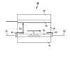
図1は、いくつかの実施形態による液晶装置100の概略図である。装置100は、第1の基板110の表面110a上に配置された第1の電極115と、第1の電極115に対抗する第2の基板120の表面120a上に配置された第2の電極125を有する第2の基板120とを含む。基板110、120の一方または両方は、ガラスのような透明な材料で作ることができる。電極115、125の一方または両方は、インジウムスズ酸化物(ITO)または薄い金属層などの導電性酸化物のような透明導電体でできていてもよい。 FIG. 1 is a schematic diagram of a
液晶材料130は、第1の電極115と第2の電極125との間に配置される。第1及び第2の電極115、125は、第1及び第2の電極115、125にわたって印加される電圧が液晶材料130の配向を制御するように配設される。第1及び第2の電極115、125にわたる電圧を変化させることにより、基板110、120の一方に通常入射する光ビームの2つの直交偏光の間の光学遅延のようなLC材料の光学特性が変化する。 A
電極の抵抗は、電流が電極を介して通過するときに熱の形で電力を消散させる。電極を介する電流によって生成される抵抗熱は、液晶材料を加熱する。本明細書で開示される実施形態では、液晶材料130の配向を制御するために使用される電極115、125の少なくとも1つは、液晶材料130を抵抗加熱するためにも使用される。少なくとも1つの電極は、LC材料に隣接するセルの内部に配置される。 The resistance of the electrodes dissipates power in the form of heat when current is passed through the electrodes. Resistive heat generated by the current through the electrodes heats the liquid crystal material. In embodiments disclosed herein, at least one of the
図1に示すように、デバイス100は、電極115を介してヒータ電流Ihを供給するように構成された制御システム140を含む。制御システム140はまた、第1の電極115及び第2の電極125にわたって配向制御電圧VLCを供給するように構成されてもよい。いくつかの実施形態によれば、制御回路140は、ヒータ電流の自動開ループ制御及び/または閉ループフィードバック制御を実装するように構成されたスイッチ、センサ、及び/または制御回路及び/またはプロセッサなどの電子回路を含む。As shown in FIG. 1,
図2のブロック図に示すLCデバイス200において、制御システム240は、この実施形態では、ヒータ電極として機能する第1の電極115を介してヒータ電流Ihを供給する電圧ソース241を備える。配向制御電圧VLCを第1及び第2の電極115、125にわたって印加して、LC材料130の配向を制御することができる。In the
図2のLCデバイス200は、制御されたバイアスが電極115に印加されることができる電極115を含み、電流が抵抗Rを有する電極115を介して流れる。例えば、LCデバイス200が1cm2の面積及び1mm2/sの熱拡散率Dを有し、電圧ソース241が電圧Vを電極115にわたって印加してジュール加熱V2/Rを生成する場合、1秒の時間期間の間で、(1s)V2/Rジュールは、約0.5gの量のガラス及び付随する量のLC材料130中に堆積され、ジュール(J)当たり約2.5℃のLC材料130の温度を上昇させる。したがって、10℃の温度上昇を達成するためには、4Jが必要であろう。第1の電極115が25オーム/平方の典型的なシート抵抗を有するインジウムスズ酸化物(ITO)である場合、10Vの電圧(及び400mAの電流)を1秒の時間期間印加することによって4Jを提供することが可能である。このシナリオは、液晶セルヒータ回路にとって妥当な範囲内である。The
電極を介する電流の分布が部分的に電極のいずれかの側への電気接続の場所によって制御することができる。電極を介して流れる実質的に均一な電流シートを得るために、高導電性材料、例えば蒸発によって堆積された薄い金属もしくは金の層、または金属ペイントもしくはインクを、ソースとの電気的接続が行われる電極の両側及び/または縁部にわたって別々に堆積させることができる。図3に示すように、いくつかの構成では、LCデバイス300は、第1の電極115及び第2の電極125の一方または両方に配置された電気接点311、312を備えることができる。電気接点311、312は、電極115、125の一方または両方の均一なシートヒータ電流密度を容易にするために、電極115、125の材料よりも高い導電率を有する材料で形成される。接点311、312は、電極115、125の一方または両方の2つ以上の離間した場所に配置されてもよい。いくつかの実施形態では、接点311、312は、液晶材料130を加熱するために使用される電流を通す電極115上にのみ配置されてもよい。接点311、312は、例えば、電極115、125上に塗装または印刷された導電性の塗料もしくはインク、またはパターン化された蒸着金属膜であってもよく、またはそれらを含んでいてもよい。 The distribution of current through the electrodes can be controlled in part by the location of the electrical connections to either side of the electrodes. In order to obtain a substantially uniform current sheet flowing through the electrodes, a highly conductive material, such as a thin metal or gold layer deposited by evaporation, or a metallic paint or ink, is used to make electrical connections with the source. It can be deposited separately over both sides and/or edges of the electrodes to be applied. As shown in FIG. 3, in some configurations the
図4は、いくつかの実施形態によるジュール加熱を提供する1つの接地電極125及び1つの電極115を有するデバイス400を示す概略図である。電圧ソース241を使用して、電極115を介して電流を供給し、及び/またはLC材料の配向を制御することができる。 FIG. 4 is a schematic diagram showing a
図4の概略図に描写されるように、いくつかの実施形態によれば、LCデバイス400の制御システム440は、ヒータ電流を制御するように構成された少なくとも1つのスイッチ445を含む。制御システム440の回路は、ヒータ電極115からヒータ電流Ihを印加または除去するために、スイッチ445を閉鎖または開放構成に動作させるように構成することができる。制御システム440は、電極115を介するヒータ電流を生成する電圧とLC材料の配向を制御する電圧との間の時間多重化のためにスイッチ445を動作させることができる。制御システム400は、スイッチ445が解放しているときに配向制御電圧を印加する。この構成では、第1の電極115にわたって実質的に均一な電位が存在する。スイッチ445が閉鎖されると、電圧ソース241による電圧の印加は、電極115を介して電極115にわたる電位勾配を生成する電流を生成する。As depicted in the schematic diagram of FIG. 4, according to some embodiments, the
いくつかの実装形態では、制御システム440は、スイッチ445を操作して、パルス状のヒータ電流を提供する。ヒータ電流の印加と配向制御電圧との間の潜在的な干渉を低減するために、ヒータ電流パルスの持続時間を制限することは有用であり得る。干渉の可能性が低減された最適な加熱を提供するために、電流パルスの持続時間は、電極、液晶材料の熱時定数、及び隣接する基板またはヒータ電極に近接した隣接する基板の熱時定数に基づいて選択することができる。いくつかの実施形態では、パルスのデューティサイクルは、約10%未満、または約5%未満、または約1%未満でさえある。LCデバイスを使用するデューティサイクルまたはサイクリング時間が比較的低い場合(例えば1分毎に1秒間の熱)、LCデバイスは、用途間で冷却することができる。 In some implementations,
代替的に、デューティサイクルが高い場合、LCデバイスを機械的に大型システムに統合する断熱スタンドオフに取り付けることによって、LCデバイスを熱的に絶縁することは意味がある。LCデバイスを熱的に絶縁することで、周囲の構造に対する熱損失を少なくすることができる。例えば、周囲の構造は、LCデバイスのハウジング、フレーム、及び/または他の支持部材を含むことができる。 Alternatively, if the duty cycle is high, it makes sense to thermally insulate the LC device by mounting it on an insulating standoff that mechanically integrates it into the larger system. Thermally isolating the LC device can reduce heat loss to surrounding structures. For example, the surrounding structure can include a housing, frame, and/or other support members for the LC device.
図5は、ヒータ電極に関連付けられる基板の熱的分離を提供するLCデバイス500の実施形態を示す。 液晶デバイス500は、断熱材料からなるスタンドオフ551、552を含む。スタンドオフ551、552は、ヒータ電流Ihを運ぶ電極115に関連付けられる基板110とLCデバイス500の周囲の構造550との間に配置される。スタンドオフ551、552は、LCデバイスのクリアアパーチャを不明瞭にしないように配設することができることに留意されたい。FIG. 5 shows an embodiment of an
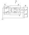
次に図4を参照すると、LCデバイス400は、ヒータ電極115を介して電圧ソース241に電気的に連結されたスイッチ445を介してヒータ電流を制御するように構成された制御システム440を含む。制御システム400は、時間多重化プロトコルを適用して、第1及び第2の電極115、125にわたる配向制御電圧を印加することと、電極115を介して電流を生成する電圧を印加することとの間の矛盾を仲介することができる。制御システム400は、スイッチ445が開放しているときに電圧ソース241に配向制御電圧を印加する。スイッチ445が閉鎖されると、電圧ソース241によって印加される電圧は、電極115を介して通過する電流を生成する。しかしながら、このシナリオでは、ヒータ電極115にわたる望ましくない電圧降下が存在し、問題となる可能性がある。 Referring now to FIG. 4,
望ましくない電圧降下を改善する方法は、図6に概略的に示されるLCデバイス600の制御システム640によって提供される。図6のデバイスは、各々の電極の一端部に印加される電流ソースと、各々の電極の反対側の端部に印加される電圧ソースとを含む。制御システム640は、2つの電流ソース642、643を制御する。各々の電流ソース642、643は、電流Iを供給する。電流ソース642は、第1の電極115の第1の場所、例えば第1の縁部に電気的に接続され、電流ソース643は、第2の電極125の第1の場所、例えば第1の縁部に電気的に接続される。第1及び第2の電極115、125の各々は、実質的に同じ縁部間抵抗Rを有することができる。したがって、各々の電極115、125の端部から端部までの電圧降下は、I*Rである。第1の電極115から第2の電極125までの電圧降下は、電圧Vを供給する電圧ソース641によって制御される。第1の電極115から第2の電極125へのこの電圧降下は、第1の電極115から第2の電極125までの任意の垂直線にわたって同じになる。したがって、電界は、液晶材料130内で実質的に均一であり、その配向を加熱とは独立して制御することができる。電流が電極115、125を介して流れるかどうかを制御するために、スイッチ645を使用することができる。なお、図6に示す構成は、各々の電極にわたる望ましくない電圧降下を最小にして、加熱及び配向制御の両方を提供することができる多くの回路構成のうちの1つであることに留意されたい。これらの回路構成は、本明細書に記載されたアプローチ内に包含されると考えられる。 A method of ameliorating the unwanted voltage drop is provided by a
図7の概略図に示されるように、いくつかの実施形態では、LCデバイス700は、加熱電極、液晶材料、または他のLCデバイス構成要素の温度を測定するように構成されたセンサ760を含むフィードバック制御システム740を備える。温度測定は、LC材料を加熱するために印加される電流を制御するためのフィードバック信号を提供するために、制御システム740によって使用され得る。 As shown in the schematic diagram of FIG. 7, in some embodiments,
いくつかの実施形態では、温度センサは、電極、LC材料、及び/またはLCデバイスの他の構成要素の抵抗を測定する4点プローブを含むことができる。測定された材料の抵抗の既知の温度係数のために、抵抗測定は、温度の代理測定を提供し、ヒータ電流を制御するために使用することができる。図7は、電流が電流ソース642によって電極115を介して供給され、センサ760によって電圧が測定される、第1の電極115の抵抗Rの4点抵抗測定構成を示す。4点抵抗測定は、抵抗Rの正確な読み出しを提供し、したがって、所望の温度を達成するために制御システム740によってヒータ電流Iを制御するために使用され得る温度測定の代用品である。このアプローチは、少なくとも検知素子がLC材料に近いため、他の方法に比べて増強された測定精度を提供する。 In some embodiments, the temperature sensor can include a four-point probe that measures the resistance of the electrodes, LC material, and/or other components of the LC device. Due to the known temperature coefficient of resistance of the measured material, resistance measurements provide a proxy measurement of temperature and can be used to control heater current. FIG. 7 shows a four-point resistance measurement configuration of the resistance R of the
本明細書で論じられるLCデバイスは、図8Aのブロック図に示されるようなハイパースペクトル撮像システム800用のスペクトルエンコーダにおける可変光学遅延器として特に有用である。図8Aのハイパースペクトル撮像機800は、画像センサ830と組み合わせて、本明細書に記載の抵抗加熱を使用して温度制御される液晶(LC)スペクトルエンコーダ810に基づく。図8Aに示され、図8Bにさらに詳細に示されているLCスペクトルエンコーダ810は、共通経路上であるが2つの直交する偏光で進む光を干渉させることによって、スペクトル情報を画像の各々の点で干渉図にエンコードする。第1の偏光子811は、入射光をLCセル810aのラビング(配列)方向に対して名目上45度の入射偏光方向に偏光させる。図8A及び図8Bに示すLCセル810aは、第1の電極812と第2の電極814との間に配置された第1のLC材料813と、第2の電極814と第3の電極816との間に配置された第2のLC材料815とを含むダブルネマチック構造である。ダブルネマチック構造では、LCセル810aの第1の半分は、LCセル810aの第2の半分に対してミラーリングされ、第1の半分は、第1のLC材料813を含み、第2の半分は、第2のLC材料815を含む。いくつかの実施形態では、第1のLC材料813及び第2のLC材料815の厚さは、ほぼ等しくてもよい。ダブルネマチック配設は、異常光線と通常光線の相対的な経路遅延がLCセル810aの両半分を介して通過するにつれて増加するが、LCセル810aの第1の半分の一次角度依存性は、LCセル810aの第2の半分の1次の角度依存性により打ち消される。 The LC devices discussed herein are particularly useful as variable optical retarders in spectral encoders for
LCセルのラビング方向は、図8Bの各々の電極812、814、816上に矢印で示され、LC材料の分子がそれに沿って配向する好ましい方向である。したがって、電極812、814、816(異常光線またはe-光線)上の方向または矢印で偏光された光は、直交偏光(通常光線またはo-光線)に対して遅延される。LCセル810aは、電気的に同調可能な複屈折素子として機能する。LCセル810aにわたる電圧を変更することによって、LC分子は、それらの配向を変化させ、e-光線とo-光線との間の可変光経路遅延を作り出すことが可能である。この経路遅延は、2つの光線間の波長依存性の位相シフトを引き起こし、それによって偏光状態の波長依存性の変化をもたらす。 The rubbing direction of the LC cell is indicated by arrows on each
第1の偏光子に対して平行または垂直に配向された第2の偏光子817またはアナライザは、この2つの光線を干渉させることによってこの波長依存性偏光状態を波長依存性の強度パターンに変化させる。(経路遅延の関数としての)強度パターンは、マイケルソン干渉計によって生成された干渉図と同等である。したがって、強度パターンは、入射光のスペクトルの余弦変換に対応する。LCセル810a上の電圧がコントローラ819によって変化される際に一連の画像を記録することにより、画像内の全ての点における干渉図を同時にサンプリングすることができ、ハイパースペクトルデータキューブは、光経路遅延軸に沿う逆余弦変換によって回復され得る。 A
コントローラ819は、電極812及び814に印加される電圧を変更することによって第1のLC材料813の配向を変更することができ、電極814及び816に印加される電圧を変更することによって第2のLC材料816の配向を変更することができる。コントローラ819は、前述したように、電極812、814、816の1つ以上を介して電流を流すことによって、抵抗加熱によってLC材料815の温度を制御することができる。
The
Claims (8)
Translated fromJapanese第1の透明基板と、
前記第1の透明基板の表面上に配置された第1の透明電極と、
第2の基板と、
前記第1の透明電極と対向する前記第2の基板の表面上に配置された第2の電極と、
前記第1の電極と第2の電極との間に印加された電圧によって液晶材料の配向を制御するように、前記第1の電極と第2の電極との間に配置された液晶材料と、
前記第1及び前記第2の電極のうちの少なくとも1つの電極を介して電流を印加して、前記液晶材料を抵抗加熱するとともに、前記第1及び前記第2の電極のうちの少なくとも1つの電極を介して電圧を印加して、前記第1の電極と前記第2の電極との間の電圧降下を制御するように構成された制御システムと、を備え、
前記電流がパルス電流であり、前記電流の電流パルスの持続時間が、前記少なくとも1つの電極、前記液晶材料、及び、前記第1の透明基板及び前記第2の基板の少なくとも一部の、熱時定数に基づいて選択される、デバイス。a device,
a first transparent substrate;
a first transparent electrode disposed on the surface of the first transparent substrate;
a second substrate;
a second electrode disposed on a surface of the second substrate facing the first transparent electrode;
a liquid crystal material disposed between the first and second electrodes such that a voltage applied between the first and second electrodes controls the orientation of the liquid crystal material;
applying a current through at least one of the first and second electrodes to resistively heat the liquid crystal material andat least one of the first and second electrodes; a control system configuredto apply a voltage across to control the voltage drop between the first electrode and the second electrode ;
wherein the current is a pulsed current, and the duration of the current pulse of the current is when the at least one electrode, the liquid crystal material, and at least a portion of the first transparent substrate and the second substrate are heated; A device that is selected based on a constant.
第1の偏光子と、
第2の偏光子と、
前記第1の偏光子と前記第2の偏光子との間に配置された液晶可変遅延器であって、
第1の透明基板と、
前記第1の透明基板の表面上に配置された第1の透明電極と、
第2の透明基板と、
前記第1の透明電極と対向する前記第2の透明基板の表面上に配置された第2の透明電極と、
前記第1の電極と前記第2の電極との間に配置された液晶材料であって、前記第1の電極及び前記第2の電極が、前記第1の電極と前記第2の電極との間に印加された電圧によって前記液晶材料の配向を制御するように配設され、前記第1の電極及び前記第2の電極のうちの少なくとも1つの電極を介して印加された電流が、前記液晶材料を抵抗加熱するとともに、前記第1及び前記第2の電極のうちの少なくとも1つの電極を介して印加された電圧が、前記第1の電極と前記第2の電極との間の電圧降下を制御する、液晶材料と、を備える、液晶可変遅延器と、
前記第2の偏光子からの光を受け取るように配設された画像センサと、を備え、
前記電流がパルス電流であり、前記電流の電流パルスの持続時間が、前記少なくとも1つの電極、前記液晶材料、及び、前記第1の透明基板及び前記第2の基板の少なくとも一部の、熱時定数に基づいて選択される、システム。A hyperspectral imaging system comprising:
a first polarizer;
a second polarizer;
A liquid crystal variable retarder disposed between the first polarizer and the second polarizer,
a first transparent substrate;
a first transparent electrode disposed on the surface of the first transparent substrate;
a second transparent substrate;
a second transparent electrode disposed on the surface of the second transparent substrate facing the first transparent electrode;
A liquid crystal material disposed between the first electrode and the second electrode, wherein the first electrode and the second electrode are aligned between the first electrode and the second electrode. arranged to control the orientation of the liquid crystal material by a voltage applied therebetween, wherein a current applied through at least one electrode of the first electrode and the second electrode causes the liquid crystal to A material is resistively heatedand a voltage applied through at least one of the first and second electrodes reduces the voltage drop between the first and second electrodes. a liquid crystal variable retarder comprising a liquid crystal material forcontrolling ;
an image sensor positioned to receive light from the second polarizer;
wherein the current is a pulsed current, and the duration of the current pulse of the current is when the at least one electrode, the liquid crystal material, and at least a portion of the first transparent substrate and the second substrate are heated; A system that is selected based on a constant.
前記第1の電極と前記第2の電極との間の電圧を制御することによって前記液晶材料の配向を制御することと、
前記第1及び前記第2の電極のうちの少なくとも1つの電極を介して電流を制御することによって、前記液晶材料を抵抗加熱するとともに、前記第1及び前記第2の電極のうちの少なくとも1つの電極を介して電圧を印加して、前記第1の電極と前記第2の電極との間の電圧降下を制御することと、を含み、
前記少なくとも1つの電極を介して電流を制御することが、パルス電流を供給することを含み、
前記電流の電流パルスの持続時間が、前記少なくとも1つの電極、前記液晶材料、及び、前記第1の透明基板及び前記第2の基板の少なくとも一部の、熱時定数に基づいて選択される、方法。A method of controlling a liquid crystal cell comprising a first transparent electrode, a second transparent electrode, and a liquid crystal material disposed between the first electrode and the second electrode, comprising:
controlling the orientation of the liquid crystal material by controlling the voltage between the first electrode and the second electrode;
Resistively heating the liquid crystal material by controlling a current through at least one ofthe first and second electrodes, and applying a voltage across electrodes to control the voltage drop between the first electrode and the second electrode ;
controlling current through the at least one electrode comprises providing a pulsed current;
the duration of the current pulse of current is selected based on thermal time constants of the at least one electrode, the liquid crystal material, and at least a portion of the first transparent substrate and the second substrate; Method.
前記検知された温度に応答して前記抵抗加熱を制御することと、を含む、請求項7に記載の方法。sensing the temperature of the liquid crystal material;
and controlling the resistive heating in response to the sensed temperature.
Applications Claiming Priority (2)
| Application Number | Priority Date | Filing Date | Title |
|---|---|---|---|
| US15/792,465 | 2017-10-24 | ||
| US15/792,465US10884278B2 (en) | 2017-10-24 | 2017-10-24 | Liquid crystal temperature control by resistive heating |
Publications (3)
| Publication Number | Publication Date |
|---|---|
| JP2019079036A JP2019079036A (en) | 2019-05-23 |
| JP2019079036A5 JP2019079036A5 (en) | 2021-11-11 |
| JP7166126B2true JP7166126B2 (en) | 2022-11-07 |
Family
ID=63965421
Family Applications (1)
| Application Number | Title | Priority Date | Filing Date |
|---|---|---|---|
| JP2018186300AActiveJP7166126B2 (en) | 2017-10-24 | 2018-10-01 | Liquid crystal temperature control by resistance heating |
Country Status (5)
| Country | Link |
|---|---|
| US (1) | US10884278B2 (en) |
| EP (1) | EP3477367A1 (en) |
| JP (1) | JP7166126B2 (en) |
| KR (2) | KR20190045832A (en) |
| CN (1) | CN109696765A (en) |
Families Citing this family (11)
| Publication number | Priority date | Publication date | Assignee | Title |
|---|---|---|---|---|
| US10564504B2 (en)* | 2017-11-30 | 2020-02-18 | Palo Alto Research Center Incorporated | Liquid-crystal variable retarder using liquid crystal cells of differing thicknesses |
| US10663346B2 (en) | 2017-12-29 | 2020-05-26 | Palo Alto Research Center Incorporated | Method and apparatus for transforming uniformly or non-uniformly sampled interferograms to produce spectral data |
| US10983338B2 (en) | 2017-12-29 | 2021-04-20 | Palo Alto Research Center Incorporated | Exit-pupil expander used distribute light over a liquid-crystal variable retarder |
| CN108267450A (en)* | 2018-02-28 | 2018-07-10 | 京东方科技集团股份有限公司 | Substrate detection apparatus and method |
| CN108983476B (en)* | 2018-08-31 | 2021-09-07 | 上海天马微电子有限公司 | Liquid crystal display panel and liquid crystal display device |
| US11828853B2 (en) | 2020-07-21 | 2023-11-28 | Leddartech Inc. | Beam-steering device particularly for LIDAR systems |
| CA3125623C (en) | 2020-07-21 | 2023-06-27 | Leddartech Inc. | Beam-steering device particularly for lidar systems |
| US11402510B2 (en) | 2020-07-21 | 2022-08-02 | Leddartech Inc. | Systems and methods for wide-angle LiDAR using non-uniform magnification optics |
| WO2022155612A1 (en)* | 2021-01-18 | 2022-07-21 | Boulder Nonlinear Systems, Inc. | Aperture heating for liquid crystal beam steering systems |
| CN113156673B (en)* | 2021-04-09 | 2023-02-28 | Tcl华星光电技术有限公司 | Alignment detection device and detection method thereof |
| GB2633139A (en)* | 2023-02-17 | 2025-03-05 | Merck Patent Gmbh | Device, method for producing a liquid crystal cell, and method for operating a device |
Citations (5)
| Publication number | Priority date | Publication date | Assignee | Title |
|---|---|---|---|---|
| JP2003329999A (en) | 2002-05-14 | 2003-11-19 | Toyota Industries Corp | Liquid crystal display |
| US20050041020A1 (en) | 2003-06-17 | 2005-02-24 | Cubic Corporation | Wide temperature range PDLC shutter |
| JP2006243063A (en) | 2005-02-28 | 2006-09-14 | Optrex Corp | Liquid crystal display device |
| JP2008287090A (en) | 2007-05-18 | 2008-11-27 | Hitachi Displays Ltd | Liquid crystal display |
| JP2016142837A (en) | 2015-01-30 | 2016-08-08 | 京セラディスプレイ株式会社 | Liquid crystal display |
Family Cites Families (23)
| Publication number | Priority date | Publication date | Assignee | Title |
|---|---|---|---|---|
| JPH0621907B2 (en)* | 1985-09-26 | 1994-03-23 | 株式会社日立製作所 | Driving method for liquid crystal display |
| US4773735A (en) | 1986-08-04 | 1988-09-27 | Allied-Signal Inc. | Fast warm-up heater for liquid crystal display |
| US4987289A (en) | 1988-07-21 | 1991-01-22 | Rockwell International Corporation | Liquid crystal display heating system |
| JPH04271323A (en)* | 1991-02-27 | 1992-09-28 | Fuji Photo Film Co Ltd | Liquid crystal display element |
| JPH05127153A (en)* | 1991-10-31 | 1993-05-25 | Canon Inc | Transparent panel heater |
| JPH0736414A (en)* | 1993-07-20 | 1995-02-07 | Sharp Corp | Liquid crystal display voltage control device |
| US5805117A (en)* | 1994-05-12 | 1998-09-08 | Samsung Electronics Co., Ltd. | Large area tiled modular display system |
| JPH10123527A (en)* | 1996-10-24 | 1998-05-15 | Canon Inc | Manufacturing method of liquid crystal element |
| US6089751A (en)* | 1996-12-30 | 2000-07-18 | Honeywell Inc. | Transparent temperature sensor for an active matrix liquid crystal display |
| JPH11271711A (en)* | 1998-03-25 | 1999-10-08 | Citizen Watch Co Ltd | Power source control circuit for driving liquid crystal |
| JP3973477B2 (en)* | 2002-04-12 | 2007-09-12 | シャープ株式会社 | Image display device |
| US6943768B2 (en)* | 2003-02-21 | 2005-09-13 | Xtellus Inc. | Thermal control system for liquid crystal cell |
| KR101131268B1 (en) | 2004-12-29 | 2012-03-30 | 엘지디스플레이 주식회사 | Liquid crystal display device |
| US6992809B1 (en)* | 2005-02-02 | 2006-01-31 | Chemimage Corporation | Multi-conjugate liquid crystal tunable filter |
| US8562871B2 (en)* | 2006-07-10 | 2013-10-22 | Sabic Innovative Plastics Ip B.V. | Composition and associated method |
| WO2008017316A1 (en) | 2006-08-08 | 2008-02-14 | Gm Global Technology Operations, Inc. | Thermally tunable liquid crystal based optical correcting element for a display |
| JP2008083217A (en)* | 2006-09-26 | 2008-04-10 | Seiko Epson Corp | Liquid crystal device |
| CN102317843A (en)* | 2009-01-30 | 2012-01-11 | 阿法密克罗有限公司 | Attachable optics arrangement and method |
| US9692209B2 (en)* | 2011-06-10 | 2017-06-27 | Massachusetts Institute Of Technology | High-concentration active doping in semiconductors and semiconductor devices produced by such doping |
| AU2014212124A1 (en)* | 2013-02-01 | 2015-09-10 | Daniel FARKAS | Method and system for characterizing tissue in three dimensions using multimode optical measurements |
| CN105408815A (en)* | 2013-03-15 | 2016-03-16 | 兰斯维克托公司 | Methods and apparatus for focus improvement in multiple liquid crystal cell lenses |
| EP3203309A1 (en)* | 2016-02-04 | 2017-08-09 | Bodle Technologies Limited | Optical device with thermally switching phase change material |
| US10768497B2 (en)* | 2016-10-03 | 2020-09-08 | Xerox Corporation | Hyperspectral imaging system |
- 2017
- 2017-10-24USUS15/792,465patent/US10884278B2/enactiveActive
- 2018
- 2018-09-30CNCN201811153644.9Apatent/CN109696765A/enactivePending
- 2018-10-01JPJP2018186300Apatent/JP7166126B2/enactiveActive
- 2018-10-08KRKR1020180119731Apatent/KR20190045832A/ennot_activeCeased
- 2018-10-23EPEP18202137.8Apatent/EP3477367A1/ennot_activeCeased
- 2022
- 2022-12-26KRKR1020220185004Apatent/KR102612631B1/enactiveActive
Patent Citations (5)
| Publication number | Priority date | Publication date | Assignee | Title |
|---|---|---|---|---|
| JP2003329999A (en) | 2002-05-14 | 2003-11-19 | Toyota Industries Corp | Liquid crystal display |
| US20050041020A1 (en) | 2003-06-17 | 2005-02-24 | Cubic Corporation | Wide temperature range PDLC shutter |
| JP2006243063A (en) | 2005-02-28 | 2006-09-14 | Optrex Corp | Liquid crystal display device |
| JP2008287090A (en) | 2007-05-18 | 2008-11-27 | Hitachi Displays Ltd | Liquid crystal display |
| JP2016142837A (en) | 2015-01-30 | 2016-08-08 | 京セラディスプレイ株式会社 | Liquid crystal display |
Also Published As
| Publication number | Publication date |
|---|---|
| KR102612631B1 (en) | 2023-12-14 |
| US10884278B2 (en) | 2021-01-05 |
| US20190121191A1 (en) | 2019-04-25 |
| CN109696765A (en) | 2019-04-30 |
| EP3477367A1 (en) | 2019-05-01 |
| KR20190045832A (en) | 2019-05-03 |
| JP2019079036A (en) | 2019-05-23 |
| KR20230007997A (en) | 2023-01-13 |
Similar Documents
| Publication | Publication Date | Title |
|---|---|---|
| JP7166126B2 (en) | Liquid crystal temperature control by resistance heating | |
| JP2019079036A5 (en) | ||
| JP6702689B2 (en) | Liquid crystal Fourier transform imaging spectrometer | |
| CA2962978C (en) | Multi-layer advanced carbon nanotube blackbody for compact, lightweight, and on-demand infrared calibration | |
| KR102430145B1 (en) | Liquid-crystal variable retarder using liquid crystal cells of differing thicknesses | |
| JP2006053551A (en) | Control system for electrochromic device | |
| WO2004077133A2 (en) | Liquid crystal cell platform | |
| US20140339407A1 (en) | Carbon nanotube blackbody film for compact, lightweight, and on-demand infrared calibration | |
| EP3215816A1 (en) | Optical measurement system | |
| US9459154B2 (en) | Multi-layer advanced carbon nanotube blackbody for compact, lightweight, and on-demand infrared calibration | |
| Harris | Characterization and application of a liquid crystal beam steering device | |
| CN112432904B (en) | Novel liquid crystal polarization modulator and detection method thereof | |
| CN107529233A (en) | A kind of heating and temperature measurement circuit based on RTD | |
| GB2126365A (en) | A method of heating an electrooptical device | |
| JPH10221669A (en) | Optical device, wavelength selection filter, and temperature control method used for these | |
| Paradis et al. | Vanadium oxide films for optical modulation applications | |
| JP2005221984A5 (en) | ||
| JPH07311085A (en) | Infrared detector | |
| Gerhard-Multhaupt et al. | Old and new poling techniques for nonlinear optical polymer electrets | |
| WO2024206081A1 (en) | Materials for temperature-actuated optical switching at infrared wavelengths | |
| JP2004125837A (en) | Variable dispersion compensator and power supply circuit thereof | |
| Renn et al. | Design of materials for molecular computing | |
| CA3143345A1 (en) | Passive infrared sensor systems and methods | |
| Zafra et al. | All-Electrical Liquid Crystal Sensors | |
| JP2014081577A (en) | Optical device and temperature control method of optical device |
Legal Events
| Date | Code | Title | Description |
|---|---|---|---|
| RD03 | Notification of appointment of power of attorney | Free format text:JAPANESE INTERMEDIATE CODE: A7423 Effective date:20181012 | |
| RD04 | Notification of resignation of power of attorney | Free format text:JAPANESE INTERMEDIATE CODE: A7424 Effective date:20181016 | |
| A521 | Request for written amendment filed | Free format text:JAPANESE INTERMEDIATE CODE: A523 Effective date:20210929 | |
| A621 | Written request for application examination | Free format text:JAPANESE INTERMEDIATE CODE: A621 Effective date:20210929 | |
| A871 | Explanation of circumstances concerning accelerated examination | Free format text:JAPANESE INTERMEDIATE CODE: A871 Effective date:20210929 | |
| A131 | Notification of reasons for refusal | Free format text:JAPANESE INTERMEDIATE CODE: A131 Effective date:20211025 | |
| A521 | Request for written amendment filed | Free format text:JAPANESE INTERMEDIATE CODE: A523 Effective date:20220125 | |
| A02 | Decision of refusal | Free format text:JAPANESE INTERMEDIATE CODE: A02 Effective date:20220302 | |
| A521 | Request for written amendment filed | Free format text:JAPANESE INTERMEDIATE CODE: A523 Effective date:20220701 | |
| C60 | Trial request (containing other claim documents, opposition documents) | Free format text:JAPANESE INTERMEDIATE CODE: C60 Effective date:20220701 | |
| C11 | Written invitation by the commissioner to file amendments | Free format text:JAPANESE INTERMEDIATE CODE: C11 Effective date:20220810 | |
| A911 | Transfer to examiner for re-examination before appeal (zenchi) | Free format text:JAPANESE INTERMEDIATE CODE: A911 Effective date:20220922 | |
| C21 | Notice of transfer of a case for reconsideration by examiners before appeal proceedings | Free format text:JAPANESE INTERMEDIATE CODE: C21 Effective date:20220926 | |
| TRDD | Decision of grant or rejection written | ||
| A01 | Written decision to grant a patent or to grant a registration (utility model) | Free format text:JAPANESE INTERMEDIATE CODE: A01 Effective date:20221011 | |
| A61 | First payment of annual fees (during grant procedure) | Free format text:JAPANESE INTERMEDIATE CODE: A61 Effective date:20221025 | |
| R150 | Certificate of patent or registration of utility model | Ref document number:7166126 Country of ref document:JP Free format text:JAPANESE INTERMEDIATE CODE: R150 |