JP7159678B2 - TOUCH SWITCH SYSTEM AND TOUCH DETECTION METHOD FOR TOUCH SWITCH SYSTEM - Google Patents
TOUCH SWITCH SYSTEM AND TOUCH DETECTION METHOD FOR TOUCH SWITCH SYSTEMDownload PDFInfo
- Publication number
- JP7159678B2 JP7159678B2JP2018140584AJP2018140584AJP7159678B2JP 7159678 B2JP7159678 B2JP 7159678B2JP 2018140584 AJP2018140584 AJP 2018140584AJP 2018140584 AJP2018140584 AJP 2018140584AJP 7159678 B2JP7159678 B2JP 7159678B2
- Authority
- JP
- Japan
- Prior art keywords
- touch
- sine wave
- wave component
- drive
- signal
- Prior art date
- Legal status (The legal status is an assumption and is not a legal conclusion. Google has not performed a legal analysis and makes no representation as to the accuracy of the status listed.)
- Active
Links
Images


Landscapes
- Electronic Switches (AREA)
- Position Input By Displaying (AREA)
Description
Translated fromJapanese本開示は、タッチスイッチシステム及びタッチスイッチシステムへのタッチ検出方法に関する。 The present disclosure relates to a touch switch system and a touch detection method for the touch switch system.
タッチスイッチシステム(タッチスイッチそのもののほか、タッチスイッチに接続される駆動回路を含む)にノイズが混入すると、タッチスイッチの誤操作が生じる。具体的には例えば、実際にはタッチされていないスイッチであるにも関わらず、そのスイッチに対してタッチがされたと検出される等の誤検出が発生する。そこで、タッチの誤検出抑制技術が知られている。 If noise enters the touch switch system (including the touch switch itself and the driving circuit connected to the touch switch), erroneous operation of the touch switch occurs. Specifically, for example, an erroneous detection occurs, such as detecting that a switch has been touched even though the switch is actually not touched. In view of this, techniques for suppressing erroneous touch detection are known.
特許文献1に記載の技術では、タッチ検出データから外乱ノイズ成分がリファレンスデータとして抽出される。そして、メモリに蓄積されたタッチ検出データからリファレンスデータを減算することでタッチ成分を抽出し、タッチの有無が検出される。 In the technique described in
ところで、特許文献1に記載の技術について本発明者が検討したところ、ノイズ存在下において、依然として誤検出の可能性があることがわかった。具体的には、特にノイズ強度が大きな場合、同一の検出電極に属する各スイッチ部のうち1つのスイッチ部へのタッチがされると、隣接するスイッチ部においてもタッチがされたと誤検出する可能性があることがわかった。 By the way, when the inventor of the present invention examined the technique described in
本開示の少なくとも一実施形態は、タッチ検出精度を向上可能なタッチスイッチシステム及びタッチスイッチシステムへのタッチ検出方法を提供することを目的とする。 An object of at least one embodiment of the present disclosure is to provide a touch switch system and a touch detection method for the touch switch system that can improve touch detection accuracy.
(1)本発明の少なくとも一実施形態に係るタッチスイッチシステムは、
駆動電極と、前記駆動電極に交差する検出電極と、前記駆動電極と前記検出電極との交差部分に形成されるスイッチ部とを備えるタッチスイッチと、
前記スイッチ部へのタッチを検出するための検出部と、を備えるタッチスイッチシステムであって、
前記検出部は、
前記検出電極からの交流信号から正弦波成分及び余弦波成分を生成させるための変換部と、
同一の前記検出電極に属する前記スイッチ部を構成する各駆動電極への駆動交流電流通流時の前記変換部からの正弦波成分及び余弦波成分について、駆動交流電流未通流時の前記検出電極の前記変換部からの正弦波成分及び余弦波成分に基づいた補正を行うための信号処理部とを備える
ことを特徴とする。(1) A touch switch system according to at least one embodiment of the present invention comprises:
a touch switch comprising a drive electrode, a detection electrode intersecting the drive electrode, and a switch section formed at an intersection of the drive electrode and the detection electrode;
A touch switch system comprising a detection unit for detecting a touch on the switch unit,
The detection unit is
a conversion unit for generating a sine wave component and a cosine wave component from the AC signal from the detection electrodes;
Regarding the sine wave component and the cosine wave component from the conversion unit when the driving alternating current is flowing to each driving electrode constituting the switching unit belonging to the same detection electrode, the detection electrode when the driving alternating current is not flowing and a signal processing unit for performing correction based on the sine wave component and the cosine wave component from the transform unit.
上記(1)の構成によれば、タッチされたスイッチ部と同一の検出電極に属するスイッチ部での誤判定抑制により、タッチ検出精度を向上できる。 According to the above configuration (1), it is possible to improve touch detection accuracy by suppressing erroneous determination in the switch section belonging to the same detection electrode as the touched switch section.
(2)幾つかの実施形態では、上記(1)の構成において、
前記信号処理部は、
前記変換部からの正弦波成分及び余弦波成分を受信するための信号受信部と、
前記駆動電極への駆動交流電流未通流時の第1正弦波成分及び第1余弦波成分とオフセット係数とに基づいて、正弦波オフセット信号及び余弦波オフセット信号を決定するためのオフセット信号決定部と、
前記駆動電極への駆動交流電流通流時の第2正弦波成分と前記正弦波オフセット信号との正弦波差分を算出することにより前記補正を行うとともに、前記駆動電極への駆動交流電流通流時の第2余弦波成分と前記余弦波オフセット信号との余弦波差分を算出することにより前記補正を行うための差分算出部と、
前記正弦波差分及び前記余弦波差分から差分信号の実効値を算出するための実効値算出部と、
前記差分信号の前記実効値に基づいて前記スイッチ部へのタッチを検出するためのタッチ検出部とを備える
ことを特徴とする。(2) In some embodiments, in the configuration of (1) above,
The signal processing unit is
a signal receiver for receiving a sine wave component and a cosine wave component from the transform unit;
An offset signal determination unit for determining a sine wave offset signal and a cosine wave offset signal based on the first sine wave component and the first cosine wave component when the drive AC current is not flowing through the drive electrode and the offset coefficient. When,
The correction is performed by calculating the sine wave difference between the second sine wave component when the alternating drive current is applied to the drive electrodes and the sine wave offset signal, and the second sine wave component when the alternating drive current is applied to the drive electrodes. a difference calculator for performing the correction by calculating a cosine wave difference between two cosine wave components and the cosine wave offset signal;
an effective value calculator for calculating an effective value of a difference signal from the sine wave difference and the cosine wave difference;
a touch detection unit for detecting a touch on the switch unit based on the effective value of the difference signal.
上記(2)の構成によれば、タッチされたスイッチ部と同一の検出電極に属するスイッチ部での誤判定抑制により、タッチ検出精度を向上できる。 According to the above configuration (2), touch detection accuracy can be improved by suppressing erroneous determination in the switch section belonging to the same detection electrode as the touched switch section.
(3)幾つかの実施形態では、上記(2)の構成において、
前記オフセット信号決定部は、前記第1正弦波成分及び前記第1余弦波成分のそれぞれに前記オフセット係数を乗じることで、前記正弦波オフセット信号及び前記余弦波オフセット信号を決定するように構成された
ことを特徴とする。(3) In some embodiments, in the configuration of (2) above,
The offset signal determination unit is configured to determine the sine wave offset signal and the cosine wave offset signal by multiplying the first sine wave component and the first cosine wave component by the offset coefficient, respectively. It is characterized by
上記(3)の構成によれば、オフセット係数を乗じることにより、正弦波オフセット信号及び余弦波オフセット信号を決定できる。 According to the configuration (3) above, the sine wave offset signal and the cosine wave offset signal can be determined by multiplying the offset coefficients.
(4)幾つかの実施形態では、上記(2)又は(3)の構成において、
前記タッチ検出部は、前記差分信号の前記実効値が、タッチ検出の基準となるタッチ閾値を超えたときに前記スイッチ部へのタッチを検出するように構成された
ことを特徴とする。(4) In some embodiments, in the configuration of (2) or (3) above,
The touch detection section is configured to detect a touch on the switch section when the effective value of the difference signal exceeds a touch threshold that is a reference for touch detection.
上記(4)の構成によれば、オフセットで得られた実効値を用いて、タッチの有無を判定できる。 With configuration (4) above, the presence or absence of a touch can be determined using the effective value obtained by the offset.
(5)幾つかの実施形態では、上記(4)の構成において、
前記タッチ検出部は、前記タッチが行われた前記スイッチ部が複数存在すると判定した場合に、前記差分信号の前記実効値と前記タッチ閾値との差分が最も大きな前記スイッチ部へのタッチを検出するように構成された
ことを特徴とする。(5) In some embodiments, in the configuration of (4) above,
The touch detection unit detects a touch on the switch unit having the largest difference between the effective value of the difference signal and the touch threshold when determining that there are a plurality of the switch units to which the touch has been performed. It is characterized by being configured as follows.
上記(5)の構成によれば、差分が最も大きなスイッチ部をタッチ有と判定することにより、タッチの誤検出を低減できる。即ち、駆動周波数以外の周波数のノイズの影響により、タッチされたスイッチ部と同一の検出電極に属するスイッチ部の実効値も、タッチされたスイッチ部の実効値よりは小さいが、ノイズが無い場合より大きくなり、タッチの閾値を超える場合がある。そこで、差分が最も大きなスイッチ部をタッチ有と判定することにより、上記のようにタッチの誤検出を低減できる。 According to the above configuration (5), by determining that the switch unit with the largest difference is touched, erroneous detection of touch can be reduced. That is, due to the influence of noise of frequencies other than the driving frequency, the effective value of the switch part belonging to the same detection electrode as the touched switch part is also smaller than the effective value of the touched switch part, but it is higher than that in the absence of noise. It can grow and exceed the touch threshold. Therefore, by determining that the switch unit with the largest difference is touched, erroneous detection of touch can be reduced as described above.
(6)幾つかの実施形態では、上記(2)~(5)の何れか1の構成において、
同じ前記検出電極によって形成される前記スイッチ部において、
前記オフセット信号決定部は、
共通する前記第1正弦波成分及び前記第1余弦波成分に基づいて、前記正弦波オフセット信号及び前記余弦波オフセット信号を決定するとともに、
前記スイッチ部毎に固有の前記オフセット係数に基づいて、前記正弦波オフセット信号及び前記余弦波オフセット信号を決定するように構成された
ことを特徴とする。(6) In some embodiments, in the configuration of any one of (2) to (5) above,
In the switch section formed by the same detection electrodes,
The offset signal determination unit,
determining the sine wave offset signal and the cosine wave offset signal based on the common first sine wave component and the first cosine wave component;
It is characterized in that the sine wave offset signal and the cosine wave offset signal are determined based on the offset coefficient unique to each switch unit.
上記(6)の構成によれば、スイッチ部へのタッチ検出精度を高めることができる。 According to the configuration (6) above, it is possible to improve the accuracy of detecting a touch to the switch section.
(7)幾つかの実施形態では、上記(1)~(6)の何れか1の構成において、
前記検出部は、
第1駆動周波数を有する第1駆動交流電流と、第2駆動周波数を有する第2駆動交流電流とを相互に切り替えて通流させるための駆動交流電流切替部を備え、
前記第1駆動周波数及び前記第2駆動周波数は、前記第1駆動交流電流の通流により得られる第1差分信号と前記第2駆動交流電流の通流により得られる第2差分信号とを同一のグラフにプロットしたときに、前記第1駆動周波数と前記第2駆動周波数との間の周波数帯において、タッチ検出の基準となるタッチ閾値以上の領域が形成されるように設定される
ことを特徴とする。(7) In some embodiments, in the configuration of any one of (1) to (6) above,
The detection unit is
a driving alternating current switching unit for switching between a first driving alternating current having a first driving frequency and a second driving alternating current having a second driving frequency, and
The first driving frequency and the second driving frequency are the same for the first differential signal obtained by passing the first alternating driving current and the second differential signal obtained by passing the second alternating driving current. characterized in that, when plotted on a graph, in a frequency band between the first drive frequency and the second drive frequency, a region above a touch threshold, which is a reference for touch detection, is formed. do.
上記(7)の構成によれば、駆動周波数と同じ又は近い周波数のノイズの存在下においても、タッチ検出の精度を高めることができる。即ち、タッチのオン及びオフの決定は、複数の駆動周波数での実効値を交互に複数回測定することで行われる。そして、駆動周波数ごとに無駆動全検出(後記する)を行い、駆動周波数の変化量がノイズ閾値以上の場合には、一定期間その駆動周波数を用いたタッチ検出を行わないようにできる。そして、他の2以上の駆動周波数を用いてタッチ検出を行うことができる。これにより、駆動周波数と同じ又は近い周波数のノイズの存在下においても、タッチ検出の精度を高めることができる。 According to the configuration (7) above, it is possible to improve the accuracy of touch detection even in the presence of noise having a frequency equal to or close to the driving frequency. In other words, touch ON and OFF decisions are made by alternately measuring the effective values at multiple drive frequencies multiple times. Then, non-drive all detection (described later) is performed for each drive frequency, and when the amount of change in the drive frequency is equal to or greater than the noise threshold, touch detection using that drive frequency can be disabled for a certain period of time. Then, touch detection can be performed using two or more other driving frequencies. As a result, touch detection accuracy can be improved even in the presence of noise having a frequency equal to or close to the drive frequency.
(8)本発明の少なくとも一実施形態に係るタッチスイッチシステムへのタッチ検出方法は、
駆動電極と、前記駆動電極に交差する検出電極と、前記駆動電極と前記検出電極との交差部分に形成されるスイッチ部とを備えるタッチスイッチと、
前記スイッチ部へのタッチを検出するための検出部と、を備えるタッチスイッチシステムへのタッチ検出方法であって、
前記検出電極からの交流信号から正弦波成分及び余弦波成分を生成させる変換ステップと、
同一の前記検出電極に属する前記スイッチ部を構成する各駆動電極への駆動交流電流通流時の前記変換ステップにおいて生成した正弦波成分及び余弦波成分について、駆動交流電流未通流時の前記検出電極の前記変換ステップで生成した正弦波成分及び余弦波成分に基づいた補正を行う信号処理ステップとを含む
ことを特徴とする。(8) A touch detection method for a touch switch system according to at least one embodiment of the present invention comprises:
a touch switch comprising a drive electrode, a detection electrode intersecting the drive electrode, and a switch section formed at an intersection of the drive electrode and the detection electrode;
A touch detection method for a touch switch system, comprising: a detection unit for detecting a touch on the switch unit;
a transforming step that produces a sine wave component and a cosine wave component from an alternating signal from the sensing electrodes;
Regarding the sine wave component and the cosine wave component generated in the conversion step when the driving alternating current is applied to each of the driving electrodes constituting the switch section belonging to the same detection electrode, the detection electrode when the driving alternating current is not applied and a signal processing step of performing correction based on the sine wave component and the cosine wave component generated in the transforming step of.
上記(8)の方法によれば、タッチされたスイッチ部と同一の検出電極に属するスイッチ部での誤判定抑制により、タッチ検出精度を向上できる。 According to the above method (8), touch detection accuracy can be improved by suppressing erroneous determinations in the switch section belonging to the same detection electrode as the touched switch section.
(9)幾つかの実施形態では、上記(8)の方法において、
前記信号処理ステップは、
前記変換ステップで生成した正弦波成分及び余弦波成分を受信する信号受信ステップと、
前記駆動電極への駆動交流電流未通流時の第1正弦波成分及び第1余弦波成分とオフセット係数とに基づいて、正弦波オフセット信号及び余弦波オフセット信号を決定するオフセット信号決定ステップと、
前記駆動電極への駆動交流電流通流時の第2正弦波成分と前記正弦波オフセット信号との正弦波差分を算出することにより前記補正を行うとともに、前記駆動電極への駆動交流電流通流時の第2余弦波成分と前記余弦波オフセット信号との余弦波差分を算出することにより前記補正を行う差分算出ステップと、
前記正弦波差分及び前記余弦波差分から差分信号の実効値を算出する実効値算出ステップと、
前記差分信号の前記実効値に基づいて前記スイッチ部へのタッチを検出するタッチ検出ステップとを含む
ことを特徴とする。(9) In some embodiments, in the method of (8) above,
The signal processing step includes:
a signal receiving step for receiving the sine wave and cosine wave components generated in the transforming step;
an offset signal determining step of determining a sine wave offset signal and a cosine wave offset signal based on the first sine wave component and the first cosine wave component when the drive AC current is not flowing through the drive electrode and the offset coefficient;
The correction is performed by calculating the sine wave difference between the second sine wave component when the alternating drive current is applied to the drive electrodes and the sine wave offset signal, and the second sine wave component when the alternating drive current is applied to the drive electrodes. a difference calculation step of performing the correction by calculating a cosine wave difference between two cosine wave components and the cosine wave offset signal;
an effective value calculation step of calculating an effective value of a difference signal from the sine wave difference and the cosine wave difference;
and a touch detection step of detecting a touch on the switch unit based on the effective value of the difference signal.
上記(9)の方法によれば、タッチされたスイッチ部と同一の検出電極に属するスイッチ部での誤判定抑制により、タッチ検出精度を向上できる。 According to the method (9) above, it is possible to improve touch detection accuracy by suppressing erroneous determination in the switch section belonging to the same detection electrode as the touched switch section.
(10)幾つかの実施形態では、上記(9)の方法において、
前記スイッチ部へのタッチ時及び無タッチ時の前記正弦波成分及び前記余弦波成分を記録する記録ステップと、
記録された前記正弦波成分及び前記余弦波成分から算出される前記実効値のうち、タッチ時の実効値のみが、タッチ検出の基準となるタッチ閾値を超えるような前記オフセット係数を決定するオフセット係数決定ステップとを含む
ことを特徴とする。(10) In some embodiments, in the method of (9) above,
a recording step of recording the sine wave component and the cosine wave component when the switch unit is touched and not touched;
Of the effective values calculated from the recorded sine wave component and the cosine wave component, only the effective value at the time of touch exceeds the touch threshold used as a reference for touch detection. and a determining step.
上記(10)の方法によれば、オフセット係数を決定できる。 According to the method (10) above, the offset coefficient can be determined.
本開示の少なくとも一実施形態によれば、ノイズ存在下においてもタッチ検出精度を向上可能なタッチスイッチシステム及びタッチスイッチシステムへのタッチ検出方法を提供できる。 According to at least one embodiment of the present disclosure, it is possible to provide a touch switch system capable of improving touch detection accuracy even in the presence of noise, and a touch detection method for the touch switch system.
以下、添付図面を参照して本発明の幾つかの実施形態について説明する。ただし、以下に実施形態として記載されている内容又は図面に記載されている内容は、あくまでも例示に過ぎず、本発明の要旨を逸脱しない範囲内で、任意に変更して実施することができる。また、各実施形態は、2つ以上を任意に組み合わせて実施することができる。さらに、各実施形態において、共通する部材については同じ符号を付すものとし、説明の簡略化のために重複する説明は省略する。 Several embodiments of the present invention will now be described with reference to the accompanying drawings. However, the contents described as embodiments or the contents described in the drawings below are merely examples, and can be arbitrarily changed and implemented without departing from the scope of the present invention. Moreover, each embodiment can be implemented by combining two or more arbitrarily. Furthermore, in each embodiment, common members are denoted by the same reference numerals, and overlapping descriptions are omitted for simplification of description.
また、実施形態として記載されている又は図面に示されている構成部品の寸法、材質、形状、その相対的配置等は、本発明の範囲をこれに限定する趣旨ではなく、単なる説明例にすぎない。
例えば、「ある方向に」、「ある方向に沿って」、「平行」、「直交」、「中心」、「同心」或いは「同軸」等の相対的或いは絶対的な配置を表す表現は、厳密にそのような配置を表すのみならず、公差、若しくは、同じ機能が得られる程度の角度や距離をもって相対的に変位している状態も表すものとする。
例えば、「同一」、「等しい」及び「均質」等の物事が等しい状態であることを表す表現は、厳密に等しい状態を表すのみならず、公差、若しくは、同じ機能が得られる程度の差が存在している状態も表すものとする。
例えば、四角形状や円筒形状等の形状を表す表現は、幾何学的に厳密な意味での四角形状や円筒形状等の形状を表すのみならず、同じ効果が得られる範囲で、凹凸部や面取り部等を含む形状も表すものとする。
一方、一の構成要素を「備える」、「具える」、「具備する」、「含む」、又は、「有する」という表現は、他の構成要素の存在を除外する排他的な表現ではない。In addition, the dimensions, materials, shapes, relative arrangements, etc. of components described as embodiments or shown in the drawings are not intended to limit the scope of the present invention, but are merely illustrative examples. do not have.
For example, expressions denoting relative or absolute arrangements such as "in a direction", "along a direction", "parallel", "perpendicular", "center", "concentric" or "coaxial" are strictly not only represents such an arrangement, but also represents a state of relative displacement with a tolerance or an angle or distance to the extent that the same function can be obtained.
For example, expressions such as "identical", "equal", and "homogeneous", which express that things are in the same state, not only express the state of being strictly equal, but also have tolerances or differences to the extent that the same function can be obtained. It shall also represent the existing state.
For example, expressions that express shapes such as squares and cylinders do not only represent shapes such as squares and cylinders in a geometrically strict sense, but also include irregularities and chamfers to the extent that the same effect can be obtained. The shape including the part etc. shall also be represented.
On the other hand, the expressions "comprising", "comprising", "having", "including", or "having" one component are not exclusive expressions excluding the presence of other components.
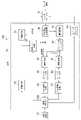
図1は、本発明の一実施形態に係るタッチスイッチシステムのブロック図である。タッチスイッチシステム100は、スイッチ部11(後記する)を備えるタッチスイッチ10と、スイッチ部11へのタッチを検出するための検出部50とを備える。検出部50は、スイッチ部11へのタッチを検出したときに、当該タッチによる入力指示を外部機器70に伝達する。これにより、外部機器70が、タッチスイッチ10へのタッチに基づいて制御される。なお、ここでいう外部機器70とは、例えばアミューズメント機器、家電、医療機器、セキュリティ関連機器、現金自動預け払い機、券売機等である。 FIG. 1 is a block diagram of a touch switch system according to one embodiment of the invention. The
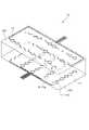
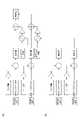
図2は、タッチスイッチ10の上面図である。タッチスイッチ10は、相互容量方式の静電式タッチスイッチである。タッチスイッチ10は、駆動電極12と、駆動電極12に交差する検出電極13と、駆動電極12と検出電極13との交差部分に形成されるスイッチ部11とを備える。駆動電極12及び検出電極13は例えばアルミニウム箔等により形成される。また、詳細は図3を参照しながら後記するが、駆動電極12と検出電極13とは異なる面に形成され、これらは電気的に導通していない。 FIG. 2 is a top view of the
タッチスイッチ10は、例えば、14個のスイッチ部11を含んで構成される。それぞれのスイッチ部11は、駆動電極12の一部を構成する、菱形形状の2つのタッチ部と、検出電極13の一部を構成する、菱形形状の2つのタッチ部とにより構成される。スイッチ部11は、左右方向に2つ又は3つずつ、上下方向に5つ配置される。これらのうち、スイッチ部11は、左右方向には、最上段において2つ、残りの段において3つずつ配置される。 The
駆動電極12は、縦方向に3本配置され、紙面右横方向に引き出される。一方で、検出電極13は、横方向に5本配置され、紙面左方向に引き出される。そして、スイッチ部11は駆動電極12と検出電極13との交差部分に形成されるため、縦方向に並ぶスイッチ部11は、同一の駆動電極12に属する。例えば、紙面左端に並ぶスイッチ部11a,11b,11c,11d,11eは、同一の駆動電極12に属する。また、横方向に並ぶスイッチ部11は、同一の検出電極13に属する。例えば、最下段に並ぶスイッチ部11a,11f,11gは、同一の検出電極13に属する。 Three
図3は、タッチスイッチ10の分解斜視図である。駆動電極12は、透明樹脂製のフィルム121上に形成される。一方で、検出電極13も、透明樹脂製のフィルム131上に形成される。駆動電極12のフィルム121への形成パターン、及び、検出電極13のフィルム131への形成パターンは、フィルム121とフィルム131とを重ね合わせた際に、上面視で上記の図2示すような形状になるように形成される。従って、フィルム121とフィルム131とを重ね合わせることで、タッチスイッチ10が得られる。 FIG. 3 is an exploded perspective view of the
タッチスイッチ10では、駆動電極12に対して駆動交流電流を流した際の検出電極13の実効値(後記する)の変化に基づき、各スイッチ部11へのタッチ検出が行われる。この際、駆動電極12に対する駆動交流電流未通流時(無駆動)の検出電極13の実効値の変化に基づいても、各スイッチ部11へのタッチ検出が行われる。 In the
図1に戻って、検出部50は、検出電極13からの交流信号から正弦波成分及び余弦波成分を生成させるための変換部50Aと、信号処理部50Bとを備える。変換部50Aは、発振回路52と、増幅回路53と、位相シフト回路54と、電流電圧変換回路55と、増幅回路56と、バンドパスフィルタ57と、掛算回路58,ローパスフィルタ59,62と、AD変換回路60,63(アナログデジタル変換回路)とを備える。 Returning to FIG. 1, the
また、これら以外にも、検出部50は、駆動交流信号を送信する対象となる駆動電極12、及び、交流信号を受信する対象となる検出電極13を切り替えるためのスイッチセレクタ64を備える。さらに、検出部50は、ソフトウェアにより信号処理を行うための信号処理部50Bを備える。信号処理部50Bについて、図4を参照しながら説明を行う。 In addition to these, the
図4は、信号処理部50Bを含む検出部50の構成を示すブロック図である。図4では、図示の簡略化のために、スイッチセレクタ64は図示していない。信号処理部50Bは、同一の検出電極13に属するスイッチ部11を構成する各駆動電極12への駆動交流電流通流時の変換部50Aからの正弦波成分及び余弦波成分について、駆動交流電流未通流時の検出電極13の変換部50Aからの正弦波成分及び余弦波成分に基づいた補正を行うためのものである。このため、信号処理部50Bは、信号受信部501と、オフセット信号決定部502と、差分算出部503と、実効値算出部504と、タッチ検出部505と、駆動交流電流切替部506と、記録データベース507とを備える。 FIG. 4 is a block diagram showing the configuration of the
信号受信部501は、変換部50Aからの正弦波成分及び余弦波成分を受信するためのものである。詳細は後記するが、検出電極13から受信した交流電流は、正弦波成分及び余弦波成分に変換される。そこで、信号受信部501は、検出電極13から出力された交流電流として、その交流電流を数値化した正弦波成分及び余弦波成分の各信号を受信する。 The
信号受信部501による受信は、駆動電極12への駆動交流電流の通流時及び未通流時のそれぞれにおいて生成した信号毎に行われる。即ち、例えば駆動交流電流の周波数(駆動周波数)が複数であれば、各駆動周波数の駆動交流電流の通流時に生成した正弦波成分及び余弦波成分が、スイッチ部11毎に受信される。なお、駆動交流電流の切り替えは、後記する駆動交流電流切替部506によって行われる。 Reception by the
オフセット信号決定部502は、駆動電極12への駆動交流電流未通流時の第1正弦波成分及び第1余弦波成分とオフセット係数とに基づいて、正弦波オフセット信号及び余弦波オフセット信号を決定するためのものである。具体的には、オフセット信号決定部502は、第1正弦波成分及び第1余弦波成分のそれぞれにオフセット係数を乗じることで、正弦波オフセット信号及び余弦波オフセット信号を決定するように構成される。オフセット信号決定部502においてオフセット係数を乗じることにより、正弦波オフセット信号及び余弦波オフセット信号を決定できる。なお、ここでいうオフセット係数は、後記する図7に示す方法により決定される。 The offset
また、同じ検出電極13によって形成されるスイッチ部11において、オフセット信号決定部502は、共通する第1正弦波成分及び第1余弦波成分に基づいて、正弦波オフセット信号及び余弦波オフセット信号を決定するとともに、スイッチ部11毎に固有のオフセット係数に基づいて、正弦波オフセット信号及び余弦波オフセット信号を決定するように構成される。このようにすることで、スイッチ部11へのタッチ検出精度を高めることができる。 Also, in the switch section 11 formed by the
差分算出部503は、駆動電極12への駆動交流電流通流時の第2正弦波成分と前記正弦波オフセット信号との正弦波差分を算出することにより上記の補正を行うとともに、駆動電極12への駆動交流電流通流時の第2余弦波成分と余弦波オフセット信号との余弦波差分を算出することにより上記の補正を行うためのものである。以下、正弦波差分及び余弦波差分を総称して差分信号ということがある。 The
実効値算出部504は、差分算出部503において算出された正弦波差分及び余弦波差分から差分信号の実効値を算出するためのものである。実効値は、例えば、横軸を余弦波成分の大きさ、縦軸を正弦波成分の大きさとする直交座標系に差分信号をプロットし、当該プロットから原点までの距離を実効値として算出することができる。 The
タッチ検出部505は、差分信号の実効値に基づいてスイッチ部11へのタッチを検出するためのものである。具体的には、タッチ検出部505は、差分信号の実効値が、タッチ検出の基準となるタッチ閾値を超えたときにスイッチ部11へのタッチを検出するように構成される。これにより、オフセットで得られた実効値を用いて、タッチの有無を判定できる。ここで、スイッチ部11毎の差分信号の実効値を正規化(後記する)し、この正規化した値に適応したタッチ閾値をタッチの検出の基準としても良い。 The
また、タッチ検出部505は、タッチが行われたスイッチ部11が複数存在すると判定した場合に、差分信号の実効値とタッチ閾値との差分が最も大きなスイッチ部11へのタッチを検出するように構成される。このようにすることで、差分が最も大きなスイッチ部11をタッチ有と判定することにより、タッチの誤検出を低減できる。即ち、駆動周波数以外の周波数のノイズの影響により、タッチされたスイッチ部11と同一の検出電極13に属するスイッチ部11の実効値も、タッチされたスイッチ部11の実効値よりは小さいが、ノイズが無い場合より大きくなり、タッチの閾値を超える場合がある。そこで、差分が最も大きなスイッチ部11をタッチ有と判定することにより、上記のようにタッチの誤検出を低減できる。 Further, when the
駆動交流電流切替部506は、第1駆動周波数を有する第1駆動交流電流と、第2駆動周波数を有する第2駆動交流電流とを相互に切り替えて駆動電極12に通流させるためのものである。第1駆動周波数及び第2駆動周波数は、第1駆動交流電流の通流により得られる第1差分信号と第2駆動交流電流の通流により得られる第2差分信号とを同一のグラフにプロットしたときに、第1駆動周波数と第2駆動周波数との間の周波数帯において、タッチ検出の基準となるタッチ閾値以上の領域が形成されるように設定される。 The driving alternating
第1駆動交流電流と第2駆動交流電流とを切り替えて使用することで、駆動周波数と同じ又は近い周波数のノイズの存在下においても、タッチ検出の精度を高めることができる。即ち、タッチのオン及びオフの決定は、複数の駆動周波数での実効値を交互に複数回測定することで行われる。そして、駆動周波数ごとに無駆動全検出(後記する)を行い、駆動周波数の変化量がノイズ閾値以上の場合には、一定期間その駆動周波数を用いたタッチ検出を行わないようにできる。そして、他の2以上の駆動周波数を用いてタッチ検出を行うことができる。これにより、駆動周波数と同じ又は近い周波数のノイズの存在下においても、タッチ検出の精度を高めることができる。 By switching between the first drive AC current and the second drive AC current, touch detection accuracy can be improved even in the presence of noise having a frequency equal to or close to the drive frequency. In other words, touch ON and OFF decisions are made by alternately measuring the effective values at multiple drive frequencies multiple times. Then, non-drive all detection (described later) is performed for each drive frequency, and when the amount of change in the drive frequency is equal to or greater than the noise threshold, touch detection using that drive frequency can be disabled for a certain period of time. Then, touch detection can be performed using two or more other driving frequencies. As a result, touch detection accuracy can be improved even in the presence of noise having a frequency equal to or close to the driving frequency.
なお、ここでいう「全検出」とは、全ての検出電極13に接続した(各検出電極13に接続されるアナログスイッチ(図示しない)の全てをオンにした)状態のことをいう。従って、例えば「無駆動全検出」とは、駆動電極12への駆動交流電流未通流時に、検出電極13の全体から交流信号及びその交流信号から得られる正弦波成分及び余弦波成分を受信することをいう。また、「駆動」とは、駆動電極12への駆動交流電流通流時に、検出電極13から交流信号及びその交流信号から得られる正弦波成分及び余弦波成分を受信することをいう。 Here, "all detection" refers to a state in which all
記録データベース507は、取得及び算出された各情報を記録するためのものである。 The
信号処理部50Bは、いずれも図示しないが、CPU(Central Processing Unit)、ROM(Read Only Memory。例えばEEPROM、FlashROM等)、RAM(Random Access Memory)、I/F(InterFace)等を備える。そして、信号処理部50Bは、ROMに格納されている所定の制御プログラムがCPUによって実行されることにより具現化される。 The
図1に戻って、タッチスイッチシステム100における信号の流れを説明する。
まず、信号処理部50B(具体的には信号処理部50Bを構成する信号送信指令部(図示しない))は、発振回路52に対し、正弦波(sinωt)を出力すべき旨の指令を送信する。同時に、信号処理部50Bは、位相シフト回路54に対し、発振回路52からの正弦波の位相をm及び(m+π/2)ずらして変更すべき旨の指令を送信する。即ち、位相シフト回路54では、周波数が同じであるが異なる位相の信号が2つ生成する。そして、発振回路52は、正弦波を生成し、正弦波(交流信号)を位相シフト回路54に送信する。Returning to FIG. 1, the signal flow in the
First, the
位相シフト回路54に送信された正弦波の位相は、上記のように、m及び(m+π/2)だけずらされる。そして、位相をmずらされた正弦波(sin(ωt+m))は、増幅回路53及び掛算回路58に送信される。増幅回路53に送信された正弦波は、振幅が増幅された後、タッチスイッチ10の駆動電極12に送信される。増幅回路53によって増幅された振幅の信号を駆動電極12に送信することにより、タッチスイッチ10でのタッチ操作により生じる小さな静電結合を感度良く検出できる。 The sine wave transmitted to
また、位相を(m+π/2)ずらされた正弦波、即ち、余弦波(cos(ωt+m)。即ちsin(ωt+m+π/2))は掛算回路61に送信される。位相をmずらすことで、タッチ操作が行われたときの信号変化を検出し易くすることができる。なお、掛算回路58,61に入力される正弦波及び余弦波は、増幅されずにそのまま掛算回路58,61に入力される。 A sine wave whose phase is shifted by (m+π/2), that is, a cosine wave (cos(ωt+m), sin(ωt+m+π/2)) is transmitted to the
タッチスイッチ10では、スイッチセレクタ64により、駆動電極12ごとに上記の正弦波が送信される。即ち、図2に示す例では、3本の駆動電極12のそれぞれに、1本ずつ正弦波が送信される。一方で、検出電極13(図2参照)に対しては、駆動電極12から、位相差角α(後記する)だけずれた正弦波(sin(ωt+α))が伝達する。そこで、タッチスイッチ10では、スイッチセレクタ64により、検出電極13ごとに上記の正弦波が受信される。なお、位相差角αは、駆動電極12と検出電極13との間の静電結合等に起因して生じるものである。位相差角αは、スイッチ部11へのタッチ操作が行われると変化し、また、例えばタッチスイッチ10の構成等の条件によっては位相差角αが発生しない(α=0)の場合もある。なお、このαは上記mを含む値である。 In the
このように、タッチスイッチ10では、駆動電極12に対し、1本ごとに正弦波を送信する。その一方で、検出電極13からは、1本ごとに正弦波を受信する。即ち、1本の駆動電極12に正弦波が送信されている間、当該駆動電極12に交差する検出電極13の1本ずつから、正弦波が受信される。このようにすることで、3本の駆動電極12と5本の検出電極13との交差部分に形成される14個のスイッチ部11へのタッチを検出できる。 In this manner, the
なお、3本の駆動電極12のうち、正弦波を送信する対象となる駆動電極12の選択は、スイッチセレクタ64によって行われる。具体的には、増幅回路53と3本の駆動電極12との間にそれぞれ配置された3個のアナログスイッチ(図示しない)のオンオフを切り替えることで、正弦波を送信する対象となる駆動電極12に対し、正弦波を送信することができる。そして、これらのアナログスイッチの切り替えは、スイッチセレクタ64によって行われる。 The
また、検出電極13での正弦波の受信も同様であり、5本の検出電極13のうち、正弦波を受信する対象となる検出電極13の選択は、スイッチセレクタ64によって行われる。具体的には、電流電圧変換回路55と5本の検出電極13との間にそれぞれ配置された5個のアナログスイッチ(図示しない)のオンオフを切り替えることで、正弦波を受信する対象となる検出電極13において、正弦波を受信することができる。そして、これらのアナログスイッチの切り替えは、スイッチセレクタ64によって行われる。 The
タッチスイッチ10を構成する検出電極13で受信した正弦波(交流電流)は、電流電圧変換回路55に入力される。電流電圧変換回路55には、静電結合によって検出電極13に誘導された微弱な電流が入力される。一方で、電流電圧変換回路55の後段(増幅回路56等)では、電圧の高低に基づく信号処理が行われる。そこで、電流電圧変換回路55において、タッチスイッチ10において生成した電流から電圧への変換が行われる。 A sine wave (alternating current) received by the
そして、電流電圧変換回路55を経た正弦波(sin(ωt+α))は、増幅回路56で振幅を増幅されて振幅Aの正弦波(Asin(ωt+α))に変換された後、バンドパスフィルタ57で信号処理される。なお、ここでいう「A」の記載に関して、バンドパスフィルタ57に入力される信号は、増幅回路53,56、電流電圧変換回路55、タッチスイッチ10での容量結合等を経て得られた信号のため、その振幅を正確に把握することが難しい。そこで、便宜的に振幅をAとし、「Asin(ωt+α)」との表記を使用している。 The sine wave (sin(ωt+α)) that has passed through the current-
タッチスイッチシステム100では、バンドパスフィルタ57と、バンドパスフィルタ57の後段に接続される掛算回路58,61及びローパスフィルタ59,62とにより、元の正弦波の周波数以外の成分(ノイズ)が良好に除去される。ただし、バンドパスフィルタ57は備えられることが好ましいが、備えられなくてもよい。 In the
検出部50では、上記のように、タッチスイッチ10の駆動電極12及び位相シフト回路54に正弦波が送信される。そして、駆動電極12と交差する検出電極13では、タッチに起因する位相差角αを有する正弦波(Asin(ωt+α))が受信され、この正弦波は、掛算回路58,61に送信される。 In the
一方で、位相シフト回路54では、位相シフト回路54に入力された正弦波の位相をmずらした正弦波(sin(ωt+m))が出力される。これに加えて、位相シフト回路54では、位相シフト回路54に入力された正弦波の位相を(m+π/2)ずらした余弦波(cos(ωt+m))も出力される。これらのうち、正弦波は増幅回路53及び掛算回路58に送信され、余弦波は掛算回路61に送信される。 On the other hand, the
掛算回路58では、タッチスイッチ10から送信された正弦波と、位相シフト回路54から送信された正弦波とが乗じられる。これにより、以下の式(1)で表される余弦波が得られる。 The

ここで得られた余弦波(時間tで振幅が変化する)は、極めて低い周波数成分のみを通過させるローパスフィルタ59で処理される。ローパスフィルタ59での処理により、(A/2)×cos(α-m)のみが余弦波成分として抽出される。(A/2)×cos(α-m)は時間によらず一定であるから、ローパスフィルタ59での処理により、交流信号が余弦波成分に変換される。余弦波成分は、AD変換回路60において、数値化される。タッチスイッチシステム100では、ここで得られた余弦波成分に基づき、タッチ検出が行われる。 The resulting cosine wave (which varies in amplitude with time t) is processed by a low-
一方で、掛算回路61では、タッチスイッチ10から送信された正弦波と、位相シフト回路54から送信された余弦波とが乗じられる。これにより、以下の式(2)で表される正弦波が得られる。 On the other hand, the

ここで得られた正弦波(時間tで振幅が変化する)は、極めて低い周波数成分のみを通過させるローパスフィルタ62で処理される。ローパスフィルタ62での処理により、(A/2)×sin(α-m)のみが上記の第2直流信号として抽出される。(A/2)×sin(α-m)は時間によらず一定であるから、ローパスフィルタ62での処理により、交流信号が正弦波成分に変換される。正弦波成分は、AD変換回路63において、数値化される。タッチスイッチシステム100では、ここで得られた正弦波成分に基づき、タッチ検出が行われる。 The sinusoidal wave obtained here (which varies in amplitude with time t) is processed by a low-
そして、正弦波成分及び余弦波成分は信号処理部50Bに送信され、正弦波成分及び余弦波成分は記録データベース507に記録される。また、信号処理部50Bは、受信した正弦波成分及び余弦波成分についてソフトウェアによる信号処理を行い、スイッチ部11へのタッチを検出する。具体的な検出方法について、図5及び図6を参照しながら説明する。 Then, the sine wave component and the cosine wave component are transmitted to the
図5は、タッチ検出のために行われるフローを示すフローチャートである。図5に示すフローは、タッチスイッチシステムへのタッチ検出方法を示すものであり、信号処理部50Bにおいて行われる。また、図6は、信号処理部50Bでの信号処理を示すブロック図である。図6に示すブロック図は、信号処理部50Bの内部でソフトウェアによって処理される。 FIG. 5 is a flow chart showing the flow performed for touch detection. The flow shown in FIG. 5 shows a touch detection method for the touch switch system, which is performed in the
本発明の一実施形態に係るタッチスイッチシステム100へのタッチ検出方法は、検出電極13からの交流信号から正弦波成分及び余弦波成分を生成させる変換ステップ(ステップS2、ステップS4)と、同一の検出電極13に属するスイッチ部11を構成する各駆動電極12への駆動交流電流通流時の上記変換ステップにおいて生成した正弦波成分及び余弦波成分について、駆動交流電流未通流時の検出電極13の変換ステップ(ステップS2)で生成した正弦波成分及び余弦波成分に基づいた補正を行う信号処理ステップとを含む。信号処理ステップは、信号受信ステップ(ステップS2、ステップS4等)と、オフセット信号決定ステップ(ステップS6等)と、差分算出ステップ(ステップS7等)と、実効値算出ステップ(ステップS8等)と、タッチ検出ステップ(ステップS15等)とを含む。 The touch detection method for the
以下、本発明の一実施形態に係るタッチスイッチシステム100へのタッチ検出方法について、図5及び図6を参照しながら説明する。 Hereinafter, a touch detection method for the
まず、タッチスイッチシステム100の電源がオンになると、初期化部(図示しない)により、タッチスイッチシステム100の初期化が行われる(ステップS1)。初期化により、記録データベース507に記録されたデータ(正弦波成分、余弦波成分、ベース値等の各種情報)が消去され、記録データベース507がリセットされる。 First, when the
初期化後、信号送信指令部(図示しない)により発振回路52に対して正弦波の出力指令が送信され、位相シフト回路54に正弦波が送信される。そして、位相シフト回路54で生成した正弦波及び余弦波(第1参照周波数での信号)は、掛算回路58,61に送信される。なお、この時点では、位相シフト回路54で生成した正弦波は、増幅回路53には送信されない(即ち無駆動)。そして、信号受信部501は、無駆動全検出の、無駆動で検出電極13毎の、及び、駆動でスイッチ部11毎の正弦波成分及び余弦波成分をそれぞれ受信する(ステップS2、信号受信ステップ)。具体的には、信号受信部501は、上記参照周波数での信号と検出電極13からの信号とに基づく変換部50Aからの正弦波成分及び余弦波成分を受信する。 After initialization, a sine wave output command is sent to the
そして、受信した正弦波成分及び余弦波成分は、信号受信部501に記録されたローパスフィルタ(ソフトウェアにより実現される。図6参照)による処理後、ベース値として記録データベース507に記録される。ソフトウェアによるローパスフィルタ処理(ローパスフィルタのカットオフ周波数を5Hz~20Hz程度に設定)により、瞬間的に発生したノイズは除去される。そして、信号受信部501は、無タッチ時の正弦波成分及び余弦波成分を記録データベース507に記録する(記録ステップ)。また、詳細は後記するが、信号受信部501は、スイッチ部11へのタッチ時(後記する)の正弦波成分及び余弦波成分も記録データベース507に記録する(記録ステップ)。次いで、オフセット信号決定部502は、全てのスイッチ部11をオフとして設定する(ステップS3)。 The received sine wave component and cosine wave component are processed by a low-pass filter (realized by software, see FIG. 6) recorded in the
次いで、駆動交流電流切替部506により駆動交流電流の周波数を切り替えながら駆動電極12に駆動交流電流を流し、信号受信部501はスイッチ部11毎の交流電流を受信することで、スキャンが開始される(ステップS4)。スキャン開始により、無駆動全検出の、無駆動で検出電極13毎の、及び、駆動でスイッチ部11毎に、検出電極13からの交流信号から正弦波成分及び余弦波成分が生成され(変換ステップ)、スイッチ部11毎の実効値が一定時間毎に取得される。そして、信号処理部50Bによる実効値の信号処理が一定時間毎に行われる。 Next, the drive AC current is supplied to the
そして、オフセット信号決定部502は、第1駆動周波数でのデータを読み込み済みであるか否かを判断する(ステップS5)。ここでいうデータは、第1駆動周波数で計測した各スイッチ部11の正弦波成分及び余弦波成分の変化量と、第1参照周波数を掛算回路58,61に供給して得られた各スイッチ部11の正弦波成分及び余弦波成分の変化量とを含む。 Then, the offset
データを読み込み済みであれば(ステップS5のYes方向)、駆動電極12への駆動交流電流未通流時の第1正弦波成分及び第1余弦波成分とオフセット係数とに基づいて、正弦波オフセット信号及び余弦波オフセット信号を決定する(ステップS6、オフセット信号決定部)。具体的には、オフセット信号決定部502は、スイッチ部11毎に、正弦波成分及び余弦波成分に対しオフセット係数(スイッチ部11毎に設定される)を乗じることで、正弦波オフセット信号及び余弦波オフセット信号を決定する。一方で、オフセット信号決定部502は、第1駆動周波数でのデータを読み込み済みでなければ(ステップS5のNo方向)、後記するステップS10~S14を行う。 If the data has already been read (Yes direction in step S5), the sine wave offset is calculated based on the first sine wave component and the first cosine wave component when the drive AC current is not flowing to the
ここで、オフセット係数の決定方法について、図7及び図8を参照しながら説明する。 Here, a method of determining the offset coefficient will be described with reference to FIGS. 7 and 8. FIG.
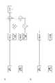
図7は、オフセット係数を決定するためにデータ収集を行うためのブロック図である。データ収集は、スイッチ部11毎に、スイッチ部11をタッチした状態で行われる。オフセット係数の決定は、例えば図示しないオフセット係数決定部により、例えば試験駆動時に行われる。図7(a)は駆動電極12に駆動交流電流を流したときのスイッチ部11毎でのブロック図、図7(b)は無駆動かつ検出電極13毎でのブロック図である。図7(a)及び(b)は同じブロック図であるため、説明の簡略化のために、図7(a)を例示して説明する。 FIG. 7 is a block diagram for collecting data to determine offset factors. Data collection is performed for each switch unit 11 while the switch unit 11 is being touched. The offset coefficient is determined by, for example, an offset coefficient determination unit (not shown) during test driving, for example. FIG. 7(a) is a block diagram of each switch section 11 when a drive AC current is applied to the
正弦波成分及び余弦波成分は、それぞれ、信号受信部501のローパスフィルタによって処理された後、それぞれのベース値(上記のベース値)を反転して加算される。そして、信号受信部501は、ベース値からの変化量を算出し、記録データベース507に記録する。これにより、データが収集される。そして、これらの操作が、駆動電極12に駆動交流電流を流したときのスイッチ部11毎(図7(a))、及び、無駆動かつ検出電極13毎(図7(b))のそれぞれについて行われる。 Each of the sine wave component and the cosine wave component is processed by the low-pass filter of the
図8は、収集されたデータに基づいてオフセット係数を決定するためのブロック図である。図8(a)は駆動電極12に駆動交流電流を流したときのスイッチ部11毎でのブロック図、図8(b)は無駆動かつ検出電極13毎でのブロック図である。図8(a)及び(b)のそれぞれにおける収集データは、図7(a)及び(b)においてそれぞれ収集されたデータに対応する。 FIG. 8 is a block diagram for determining offset factors based on collected data. FIG. 8(a) is a block diagram of each switch section 11 when a drive AC current is applied to the
オフセット係数は、例えばシミュレーションを用いたオフセット係数決定ステップにより決定される。オフセット係数決定ステップは、例えば、伝導イミュニティ試験(IEC61000-4-6)において決定できる。オフセット係数決定ステップは、記録された正弦波成分及び余弦波成分から算出される実効値のうち、タッチ時の実効値のみが、タッチ検出の基準となるタッチ閾値を超えるようなオフセット係数を決定するものである。 The offset coefficient is determined by an offset coefficient determination step using simulation, for example. The offset factor determination step can be determined, for example, in a conducted immunity test (IEC61000-4-6). The offset coefficient determination step determines an offset coefficient such that, of the effective values calculated from the recorded sine wave component and cosine wave component, only the effective value at the time of touch exceeds the touch threshold that is the reference for touch detection. It is.
図8を参照しながらオフセット係数決定ステップを説明すると、上記図7(b)での収集データである変化量と、実際にタッチが行われているときの変化量((図7(a)での収集データ)に変数としてのオフセット係数を乗じて(掛算して)得られる変化量とを比較して、これらの変化量が同じになるオフセット係数が決定される。変化量が同じになることを確認することで、タッチ検出精度が向上する。このようなオフセット係数決定ステップにより、オフセット係数を決定できる。 The offset coefficient determination step will be described with reference to FIG. 8. The amount of change that is the collected data in FIG. data) is multiplied (multiplied) by the offset coefficient as a variable and compared with the amount of change obtained, and the offset coefficient that makes these amounts of change the same is determined. Touch detection accuracy is improved by confirming the offset coefficient can be determined by such an offset coefficient determination step.
なお、オフセット係数は、以下のようにして自動で決定することもできる。まず、1つのスイッチ部11を検査棒(後記する)で押下することで、スイッチ部11へのタッチ状態が実行される。そして、タッチ状態が維持された状態で、駆動電極12への駆動交流電流の駆動周波数及びその近傍の周波数(例えば駆動周波数のプラスマイナス10%以内)以外の周波数のノイズを印加しながら、駆動状態での上記の正弦波成分及び余弦波成分に係るデータが収集される。これに加えて、タッチ状態が維持された状態で、同じ周波数帯のノイズを印加しながら、無駆動での検出電極13毎の正弦波成分及び余弦波成分に係るデータも収集される。そして、タッチ状態のスイッチ部11における実効値の変化量を正規化した値が100%になるように、当該スイッチ部11でのオフセット係数が決定される。この時点では、タッチ状態のスイッチ部11以外のスイッチ部11については考慮しない。そして、以上の処理がスイッチ部11毎に行われ、スイッチ部11毎のオフセット係数が決定される。 Note that the offset coefficient can also be determined automatically as follows. First, by pressing one switch portion 11 with an inspection stick (to be described later), the switch portion 11 is touched. Then, while the touch state is maintained, noise of a frequency other than the drive frequency of the drive AC current to the
次に、スイッチ部11毎に実際にタッチを行って得られた実効値について、決定されたオフセット係数に基づき、オフセット(補正)が行われる。そして、オフセットによりタッチを正確に検出できるかの確認が行われ、正確に検出できた場合には、決定されたオフセット係数が記録データベース507に記録される。一方で、正確に検出できない場合には、オフセット係数の補正が行われ、補正後のオフセット係数が記録データベース507に記録される。なお、ここでいう補正とは、再度、検査棒(後記する)でタッチした箇所のスイッチ部11の実効値の変化量を正規化した値が100%になるようにすることをいう。 Next, an effective value obtained by actually touching each switch unit 11 is offset (corrected) based on the determined offset coefficient. Then, it is checked whether the touch can be accurately detected by the offset, and if the touch can be accurately detected, the determined offset coefficient is recorded in the
図5及び図6に戻り、上記のステップS5において正弦波オフセット信号及び余弦波オフセット信号が決定された後、差分算出部503は、駆動電極12への駆動交流電流通流時の第2正弦波成分と正弦波オフセット信号との正弦波差分を算出することにより上記補正を行うとともに、駆動電極12への駆動交流電流通流時の第2余弦波成分と前記余弦波オフセット信号との余弦波差分を算出することにより上記補正を行う(ステップS7、差分算出ステップ)。ここでいう駆動交流電流とは、第1駆動周波数を有する交流電流のことをいう。 Returning to FIGS. 5 and 6, after the sine wave offset signal and the cosine wave offset signal are determined in step S5 above, the
そして、実効値算出部504は、正弦波差分及び余弦波差分から差分信号の実効値を算出する(ステップS8、実効値算出ステップ)。算出された実効値は、予め定められた正規化用設定値に基づき、正規化される。ここでいう正規化用設定値は、スイッチ部11毎に定められるものであり、例えば、直径10mmの検査棒を用いてタッチしたときに得られる実効値を100%として設定することができる。また、正規化用設定値は、スイッチ部11間には感度のバラツキがあり、このバラツキを補正するために、ノイズを印加しない状態(環境)で設定される。ノイズを印加しない状態で設定することで、スイッチ11間のタッチの有無を安定して検出できる。 Then, the
ここで、正弦波成分及び余弦波成分から差分信号及び実効値を算出するための流れを、別のブロック図を参照しながら説明する。 Here, the flow for calculating the difference signal and the effective value from the sine wave component and cosine wave component will be described with reference to another block diagram.
図9は、正弦波成分及び余弦波成分とオフセット係数とに基づいて実効値を算出するためのブロック図である。図9(a)は駆動電極12に駆動交流電流を流したときのスイッチ部11毎でのブロック図、図9(b)は無駆動かつ検出電極13毎でのブロック図である。上記の図7を参照しながら説明した内容と同様に、正弦波成分及び余弦波成分のそれぞれについて、ベース値からの変化量が算出される。 FIG. 9 is a block diagram for calculating an effective value based on sine wave components, cosine wave components, and offset coefficients. FIG. 9(a) is a block diagram of each switch unit 11 when a drive AC current is applied to the
そして、正弦波成分及び余弦波成分のそれぞれについて、図9(b)で得られた変化量にオフセット係数を乗じて得られた値を、図9(a)で得られた変化量から減じる。即ち、差分が算出されることで、オフセット(補正)が行われる。次いで、オフセット後の正弦波成分及び余弦波成分に基づいて、実効値が算出される。以降の処理では、算出された実効値が正規化され、正規化された実効値が、詳細は後記するが、スイッチ部11へのタッチ検出に用いられる。 Then, for each of the sine wave component and the cosine wave component, the value obtained by multiplying the amount of change obtained in FIG. 9(b) by the offset coefficient is subtracted from the amount of change obtained in FIG. 9(a). That is, offset (correction) is performed by calculating the difference. An effective value is then calculated based on the offset sine wave component and cosine wave component. In subsequent processing, the calculated effective value is normalized, and the normalized effective value is used for detecting a touch to the switch section 11, although the details will be described later.
再度図5及び図6に戻り、実効値算出部504は、実効値が予め定められたタッチ閾値以上であるスイッチ部11をオンと仮定し、実効値が予め定められた閾値未満であるスイッチ部11をオフと仮定する処理が行われる。この時点では、オン及びオフの確定はされず、後記の高強度ノイズを考慮したうえで、最終的なタッチの検出が行われる。 Returning to FIGS. 5 and 6 again, the effective
オン及びオフの仮定後、高強度ノイズが存在するか否かを判定する(ステップS9)(。具体的には、上記のステップS2において無駆動全検出時に得られた実効値が、予め定められたノイズ閾値以上であるか否かを判定する。なお、ノイズ閾値は、信号処理部50Bのローパスフィルタ(ソフトウェア)は使用しない状態で、上記の伝導イミュニティ試験によって決定できる。具体的には、ノイズ閾値としては、2つの参照周波数での無駆動全検出時に、2つの参照周波数と同じ周波数及びその近傍(例えばプラスマイナス10%以内)の周波数以外において、当該2つの参照周波数間にノイズが存在するときの実効値(タッチ時の実効値)が同程度になるときの正弦波成分及び余弦波成分に基づき算出される実効値を採用できる。 After assuming ON and OFF, it is determined whether or not high-intensity noise exists (step S9). The noise threshold can be determined by the above conduction immunity test without using the low-pass filter (software) of the signal processing unit 50B.Specifically, the noise As a threshold, noise exists between the two reference frequencies other than the same frequency as the two reference frequencies and frequencies in the vicinity thereof (for example, within plus or minus 10%) at the time of no-drive all detection at the two reference frequencies. An effective value calculated based on a sine wave component and a cosine wave component when the effective value at the time (effective value at the time of touch) is approximately the same can be employed.
さらに、ノイズ閾値は、参照周波数の3逓倍の箇所でのノイズが判断できる閾値に設定される。従って、ノイズ閾値は、参照周波数及びその3逓倍の周波数の双方におけるノイズを判定可能な値に設定される。なお、ここでは参照周波数(正弦波及び余弦波)のデューティ比が50%であり、奇数次の高調波が強く影響する。一方で、高次ではノイズの影響が小さいため、ノイズの影響が強く出易い、低次かつ奇数次である3逓倍にしている。 Furthermore, the noise threshold is set to a threshold at which noise can be determined at the point where the reference frequency is tripled. Therefore, the noise threshold is set to a value that allows determination of noise at both the reference frequency and its tripled frequency. Here, the reference frequency (sine wave and cosine wave) has a duty ratio of 50%, and odd-order harmonics have a strong influence. On the other hand, since the effect of noise is small at higher orders, the frequency is set to 3, which is a low order and an odd number, which is likely to be strongly affected by noise.
高強度ノイズが存在すると判定された場合(Yes方向)、第1駆動周波数でのデータ読み込みがすぐには確立されず、第2駆動周波数でのデータの読み込み済みを待つため、再度上記のステップS5~S8が行われる。一方で、高強度ノイズが存在しないと判定された場合(No方向)、上記のステップS5~S14が繰り返し行われる。そして、3回連続でスイッチ部11のオンオフ状態が同じであるか否かを判定する(ステップS15、タッチ検出ステップ)。又は、第1駆動周波数及び第2駆動周波数で計測した無駆動時の全ての検出電極13からの変化量の実効値が小さい駆動周波数のオンオフ状態を採用してもよい。同じでなければ、即ち変化が無ければ(No方向)、上記のステップS5以降が繰り返される。 If it is determined that high-intensity noise exists (Yes direction), the data reading at the first drive frequency is not immediately established, and in order to wait for the data reading at the second drive frequency to be completed, the above step S5 is performed again. to S8 are performed. On the other hand, if it is determined that high-intensity noise does not exist (No direction), the above steps S5 to S14 are repeated. Then, it is determined whether or not the ON/OFF state of the switch unit 11 is the same three times in succession (step S15, touch detection step). Alternatively, the ON/OFF state of the drive frequency in which the effective value of the amount of change from all the
一方、3回連続でスイッチ部11のオンオフ状態が同じであれば(Yes方向)、スイッチ部11の中にオンのスイッチ部11が存在するか否かを判定する(ステップS16)。オンのスイッチ部11が存在しなければ(No方向)、全てのスイッチ部11をオフとして、スイッチ情報が生成される(ステップS19)。しかし、オンのスイッチ部11が存在すれば(Yes方向)、オンのスイッチ部11の数が1つのみであるか否かを判定する(ステップS16)。 On the other hand, if the ON/OFF state of the switch section 11 is the same three times consecutively (Yes direction), it is determined whether or not there is an ON switch section 11 among the switch sections 11 (step S16). If there is no ON switch unit 11 (No direction), switch information is generated by turning off all the switch units 11 (step S19). However, if there is an ON switch unit 11 (Yes direction), it is determined whether or not the number of ON switch units 11 is only one (step S16).
オンのスイッチ部11の数が2つ以上であれば、即ち、タッチが行われたスイッチ部11が複数存在すると判定した場合には(No方向)、タッチ検出部505は、差分信号の実効値とタッチ閾値との差分が最も大きなスイッチ部11へのタッチを検出する(ステップS20、タッチ検出ステップ)。即ち、2キーロック処理により、オンのスイッチ部11が決定される。2キーロック処理により、タッチ後のタッチしたスイッチ部11と同じ検出電極13に属するスイッチ部11において、ノイズの影響による誤入力が抑制される。 If the number of ON switch units 11 is two or more, that is, if it is determined that there are a plurality of touched switch units 11 (No direction), the
一方で、オンのスイッチ部11の数が1つであれば、即ち、タッチが行われたスイッチ部11が1つのみ存在すると判定した場合には(Yes方向)、スイッチ部11へのタッチ検出が確定され(ステップS18)、上記のステップS4以降のフローが繰り返し行われる。そして、タッチ検出部505は、差分信号の実効値に基づいてスイッチ部11へのタッチを検出し、確定する(タッチ検出ステップ)。タッチ検出が確定したスイッチ部11の情報は外部機器70に送信される。そして、外部機器70では、受信した情報に基づいた制御が行われる。 On the other hand, if the number of ON switch units 11 is one, that is, if it is determined that there is only one touched switch unit 11 (Yes direction), touch detection to switch unit 11 is performed. is determined (step S18), and the flow after step S4 is repeated. Then, the
以上のタッチ検出方法及びタッチスイッチシステム100によれば、タッチされたスイッチ部11と同一の検出電極13に属するスイッチ部11での誤判定抑制により、タッチ検出精度を向上できる。 According to the touch detection method and the
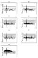
図10は、各スイッチ部11での正弦波成分を示すグラフである。また、図11は、各スイッチ部11での余弦波成分を示すグラフである。各グラフにおいて、縦軸は信号強度を表す。また、横軸は時間を表す。即ち、横軸は、ノイズの周波数150kHzから1秒単位に1%の周波数を増加したときの時間に対応し、横軸250の位置が150kHzに対応し、横軸2770の位置が273kHzに対応し、横軸7400の位置が814kHzに対応し、横軸8300の位置が1MHzに対応する。 FIG. 10 is a graph showing sine wave components in each switch section 11. In FIG. 11 is a graph showing cosine wave components in each switch section 11. FIG. In each graph, the vertical axis represents signal intensity. Also, the horizontal axis represents time. That is, the horizontal axis corresponds to the time when the frequency is increased by 1% per second from the noise frequency of 150 kHz, the position of the horizontal axis 250 corresponds to 150 kHz, and the position of the horizontal axis 2770 corresponds to 273 kHz. , the position of the horizontal axis 7400 corresponds to 814 kHz, and the position of the horizontal axis 8300 corresponds to 1 MHz.
これらのグラフは、本発明者により行われた試験により得られたものである。具体的には、上記の試験棒によるスイッチ部11aのタッチを繰り返しながら、ノイズ周波数を連続的に変更することで、上記伝導イミュニティ試験を行った。伝導イミュニティ試験の際、駆動電極12に流す駆動交流電流の駆動周波数は273kHzとした。各グラフにおいて突出したピークは、駆動周波数と、駆動周波数の3逓倍の周波数とである。ただし、駆動周波数の3逓倍の周波数については、ソフトウェアによるローパスフィルタにより、駆動周波数の3逓倍よりも小さな周波数にピークが発生している。 These graphs are obtained from tests conducted by the inventors. Specifically, the conduction immunity test was performed by continuously changing the noise frequency while repeatedly touching the switch portion 11a with the test rod. During the conduction immunity test, the drive frequency of the drive AC current applied to the
図10及び図11において、(a)はスイッチ部11aでの変化量、(b)はスイッチ部11aでの差分(正弦波差分及び余弦波差分)、(c)はスイッチ部11fでの変化量、(d)はスイッチ部11fでの差分(正弦波差分及び余弦波差分)、(e)はスイッチ部11gでの変化量、(f)はスイッチ部11gでの差分(正弦波差分及び余弦波差分)、(g)は無駆動時の全ての検出電極13からの変化量を示す。これらのうち、(b)(d)(f)は、(g)のグラフにスイッチ部11毎のオフセット係数を乗じることで得られた値を、(a)(c)(e)のグラフから減じる(オフセット後に差分を算出する)ことで得られたものである。なお、スイッチ部11a,11f,11gは同一の検出電極13に属するスイッチ部11である。 10 and 11, (a) is the amount of change in the switch section 11a, (b) is the difference (sine wave difference and cosine wave difference) in the switch section 11a, and (c) is the amount of change in the switch section 11f. , (d) is the difference (sine wave difference and cosine wave difference) at the switch section 11f, (e) is the amount of change at the switch section 11g, and (f) is the difference (sine wave difference and cosine wave difference) at the switch section 11g. difference), and (g) shows the amount of change from all the
図10(b)に示すグラフの決定に際して、オフセット係数は0.30とした。さらに、図10(d)に示すグラフの決定に際して、オフセット係数は0.15とした。そして、図10(f)に示すグラフの決定に際して、オフセット係数は0.30とした。
また、図11(b)に示すグラフの決定に際して、オフセット係数は-0.15とした。さらに、図11(d)に示すグラフの決定に際して、オフセット係数は-0.35とした。そして、図11(f)に示すグラフの決定に際して、オフセット係数は0.10とした。When determining the graph shown in FIG. 10(b), the offset coefficient was set to 0.30. Furthermore, when determining the graph shown in FIG. 10(d), the offset coefficient was set to 0.15. Then, when determining the graph shown in FIG. 10(f), the offset coefficient was set to 0.30.
Also, the offset coefficient was set to -0.15 when determining the graph shown in FIG. 11(b). Furthermore, when determining the graph shown in FIG. 11(d), the offset coefficient was set to −0.35. In determining the graph shown in FIG. 11(f), the offset coefficient was set to 0.10.
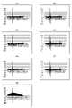
図12は、各スイッチ部11での実効値を示すグラフである。横軸は周波数、縦軸は実効値を表す。実効値(差分信号の実効値)は、上記図10及び図11に示した、オフセット後に算出された差分(正弦波差分及び余弦波差分)に基づいて算出される。 FIG. 12 is a graph showing effective values in each switch section 11. As shown in FIG. The horizontal axis represents frequency, and the vertical axis represents effective value. The effective value (effective value of the difference signal) is calculated based on the difference (sine wave difference and cosine wave difference) calculated after the offset shown in FIGS. 10 and 11 above.
図12(a)は、図10(a)及び図11(a)のグラフから得られる周波数毎の実効値の大きさ、図12(b)は、図10(b)及び図11(b)のグラフから得られる周波数毎の実効値の大きさ、図12(c)は、図10(c)及び図11(c)のグラフから得られる周波数毎の実効値の大きさ、図12(d)は、図10(d)及び図11(d)のグラフから得られる周波数毎の実効値の大きさ、図12(e)は、図10(e)及び図11(e)のグラフから得られる周波数毎の実効値の大きさ、図12(f)は、図10(f)及び図11(f)のグラフから得られる周波数毎の実効値の大きさ、図12(g)は、図10(g)及び図11(g)のグラフから得られる周波数毎の実効値の大きさを表す。 FIG. 12(a) shows the magnitude of the effective value for each frequency obtained from the graphs of FIGS. 10(a) and 11(a), and FIG. 12(b) shows FIGS. The magnitude of the effective value for each frequency obtained from the graph of FIG. 12(c) is the magnitude of the effective value for each frequency obtained from the graphs of FIGS. ) is the magnitude of the effective value for each frequency obtained from the graphs of FIGS. 10(d) and 11(d), and FIG. 12(e) is obtained from the graphs of FIGS. 12(f) is the magnitude of the effective value for each frequency obtained from the graphs of FIGS. 10(f) and 11(f), and FIG. 10(g) and 11(g) show the magnitude of the effective value for each frequency obtained from the graphs of FIG.
図12(a)(c)(e)は所謂生データであり、図12(b)(d)(f)はオフセット後の実効値である。そのため、タッチ検出は、図12(b)(d)(f)のグラフに基づいて行われる。 12(a), 12(c) and 12(e) are so-called raw data, and FIGS. 12(b), 12(d) and 12(f) are effective values after offset. Therefore, touch detection is performed based on the graphs of FIGS. 12(b), (d) and (f).
例えば、所謂生データである図12(a)(c)(e)に基づきタッチ検出を行う場合を考える。実際にはスイッチ部11aのみがタッチされた場合、タッチ閾値を200(図12において太い破線で示す値)とすれば、図12(a)(c)で200を超える周波数があるため、スイッチ部11a,11fの双方でタッチ検出が行われたと判断される。従って、この場合には、誤ったタッチ検出が行われる。 For example, consider a case where touch detection is performed based on so-called raw data in FIGS. In practice, when only the switch portion 11a is touched, if the touch threshold is set to 200 (the value indicated by the thick dashed line in FIG. 12), there are frequencies exceeding 200 in FIGS. It is determined that touch detection has been performed in both 11a and 11f. Therefore, in this case, erroneous touch detection is performed.
しかし、図12(b)(d)(f)に示すようにオフセット後の信号強度に基づきタッチ検出が行われることで、実際にタッチが行われたスイッチ部11aに対応する図12(a)のグラフのみで、実効値を200以上にできる。これにより、タッチの誤検出を抑制できる。従って、予め定められたオフセット係数と、無駆動かつ全ての検出電極13の正弦波成分及び余弦波成分とを用いて差分を算出することで、タッチ精度を向上できる。 However, as shown in FIGS. 12(b), 12(d), and 12(f), touch detection is performed based on the signal intensity after the offset, so that FIG. The effective value can be 200 or more with only the graph of . As a result, erroneous touch detection can be suppressed. Therefore, touch accuracy can be improved by calculating the difference using a predetermined offset coefficient and the sine wave component and cosine wave component of all
この理由は、本発明者の推測によれば、例えば以下の理由であると考えられる。 According to the speculation of the present inventor, the reason for this is considered to be, for example, the following.
タッチスイッチシステム100では、駆動交流電流が駆動電極12に通流され、検出電極13からの交流電流が受信される。そして、タッチスイッチ100は、本発明の一実施形態では、グラウンド(GND)に接続されていない。そのため、機器設置前の伝導イミュニティ試験においてスイッチ部11に人がタッチする際に人は接地しているが、機器設置後の通常駆動時においてノイズが印加される際にタッチスイッチ100はグラウンドに接続されていない。このため、駆動周波数に対してプラスマイナス数百kHz以上の範囲において、ノイズの印加状態が等価ではない状態が発生すると考えられる。そこで、本発明の一実施形態では、上記のように、ソフトウェアにより、予め定められたオフセット係数と、無駆動かつ全ての検出電極13の正弦波成分及び余弦波成分とを用いて差分を算出することで、タッチ精度の向上が図られる。 In
図13は、第2実施形態において、駆動周波数を切り替える際の信号流れを示すブロック図である。第2実施形態では、上記の図6に示した第1実施形態とは異なり、無駆動全検出においてノイズ閾値との比較が行われない。即ち、第1駆動周波数及び第2駆動周波数のそれぞれについてノイズの計測値がノイズ閾値以下の場合、第1駆動周波数及び第2駆動周波数で計測したスイッチ部11の実効値が交互に判断される。従って、第1駆動周波数及び第2駆動周波数の双方で計測したスイッチ部11の実効値がタッチの検出に利用される。一方で、第1駆動周波数及び第2駆動周波数のうち、ノイズの計測値がノイズ閾値を超える場合、そのノイズに対応する駆動周波数でのスイッチ部11の実効値は利用されない。 FIG. 13 is a block diagram showing the signal flow when switching the drive frequency in the second embodiment. In the second embodiment, unlike the first embodiment shown in FIG. 6, no comparison with the noise threshold is performed in no-drive all detection. That is, when the noise measurement values for each of the first drive frequency and the second drive frequency are equal to or less than the noise threshold, the effective values of the switch section 11 measured at the first drive frequency and the second drive frequency are alternately determined. Therefore, the effective value of the switch section 11 measured at both the first drive frequency and the second drive frequency is used for touch detection. On the other hand, if the measured value of noise exceeds the noise threshold at the first drive frequency and the second drive frequency, the effective value of the switch section 11 at the drive frequency corresponding to the noise is not used.
なお、無駆動全検出で得られた正弦波成分及び余弦波成分のうち、駆動周波数におけるノイズが小さな方の正弦波成分及び余弦波成分が採用され、採用された正弦波成分及び余弦波成分に基づき、タッチ検出が行われるようにしてもよい。このようにすることで、信号処理を簡便にできる。 Of the sine wave components and cosine wave components obtained by no-drive all detection, the sine wave component and cosine wave component with smaller noise at the drive frequency are adopted, and the adopted sine wave component and cosine wave component are Based on this, touch detection may be performed. By doing so, the signal processing can be simplified.
10 タッチスイッチ
11,11a,11b,11c,11d,11e,11f,11g スイッチ部
12 駆動電極
13 検出電極
50 検出部
50A 変換部
50B,51B 信号処理部
52 発振回路
53,56 増幅回路
54 位相シフト回路
55 電流電圧変換回路
57 バンドパスフィルタ
58,61 掛算回路
59,62 ローパスフィルタ
60,63 変換回路
64 スイッチセレクタ
70 外部機器
100 タッチスイッチシステム
121,131 フィルム
501 信号受信部
502 オフセット信号決定部
503 差分算出部
504 実効値算出部
505 タッチ検出部
506 駆動交流電流切替部
507 記録データベース10 touch switches 11, 11a, 11b, 11c, 11d, 11e, 11f,
Claims (10)
Translated fromJapanese前記スイッチ部へのタッチを検出するための検出部と、を備えるタッチスイッチシステムであって、
前記検出部は、
前記検出電極からの交流信号から正弦波成分及び余弦波成分を生成させるための変換部と、
同一の前記検出電極に属する前記スイッチ部を構成する各駆動電極への駆動交流電流通流時の前記変換部からの正弦波成分及び余弦波成分について、駆動交流電流未通流時の前記検出電極の前記変換部からの正弦波成分及び余弦波成分に基づいた補正を行うための信号処理部とを備え、
前記信号処理部は、
前記駆動電極への駆動交流電流未通流時の第1正弦波成分及び第1余弦波成分と、前記スイッチ部毎に固有のオフセット係数とに基づいて正弦波オフセット信号及び余弦波オフセット信号を決定し、
前記正弦波オフセット信号に基づき、前記駆動電極への駆動交流電流通流時の前記正弦波成分の補正を行い、
前記余弦波オフセット信号に基づき、前記駆動電極への駆動交流電流通流時の前記余弦波成分の補正を行う
ように構成された
ことを特徴とする、タッチスイッチシステム。a touch switch comprising a drive electrode, a detection electrode intersecting the drive electrode, and a switch section formed at an intersection of the drive electrode and the detection electrode;
A touch switch system comprising a detection unit for detecting a touch on the switch unit,
The detection unit is
a conversion unit for generating a sine wave component and a cosine wave component from the AC signal from the detection electrodes;
Regarding the sine wave component and the cosine wave component from the conversion unit when the driving alternating current is flowing to each driving electrode constituting the switching unit belonging to the same detection electrode, the detection electrode when the driving alternating current is not flowing a signal processing unit for performing correction based on the sine wave component and the cosine wave component from the transform unit;
The signal processing unit is
A sine wave offset signal and a cosine wave offset signal are determined based on a first sine wave component and a first cosine wave component when the drive AC current is not applied to the drive electrode, and an offset coefficient specific to each of the switch units. death,
Based on the sine wave offset signal, correcting the sine wave component when the drive alternating current is applied to the drive electrode,
Based on the cosine wave offset signal, the cosine wave component is corrected when the drive alternating current is applied to the drive electrode.
configured as
A touch switch system characterized by:
前記スイッチ部へのタッチを検出するための検出部と、を備えるタッチスイッチシステムであって、
前記検出部は、
前記検出電極からの交流信号から正弦波成分及び余弦波成分を生成させるための変換部と、
同一の前記検出電極に属する前記スイッチ部を構成する各駆動電極への駆動交流電流通流時の前記変換部からの正弦波成分及び余弦波成分について、駆動交流電流未通流時の前記検出電極の前記変換部からの正弦波成分及び余弦波成分に基づいた補正を行うための信号処理部とを備え、
前記信号処理部は、
前記変換部からの正弦波成分及び余弦波成分を受信するための信号受信部と、
前記駆動電極への駆動交流電流未通流時の第1正弦波成分及び第1余弦波成分とオフセット係数とに基づいて、正弦波オフセット信号及び余弦波オフセット信号を決定するためのオフセット信号決定部と、
前記駆動電極への駆動交流電流通流時の第2正弦波成分と前記正弦波オフセット信号との正弦波差分を算出することにより前記補正を行うとともに、前記駆動電極への駆動交流電流通流時の第2余弦波成分と前記余弦波オフセット信号との余弦波差分を算出することにより前記補正を行うための差分算出部と、
前記正弦波差分及び前記余弦波差分から差分信号の実効値を算出するための実効値算出部と、
前記差分信号の前記実効値に基づいて前記スイッチ部へのタッチを検出するためのタッチ検出部とを備える
ことを特徴とするタッチスイッチシステム。a touch switch comprising a drive electrode, a detection electrode intersecting the drive electrode, and a switch section formed at an intersection of the drive electrode and the detection electrode;
A touch switch system comprising a detection unit for detecting a touch on the switch unit,
The detection unit is
a conversion unit for generating a sine wave component and a cosine wave component from the AC signal from the detection electrodes;
Regarding the sine wave component and the cosine wave component from the conversion unit when the driving alternating current is flowing to each driving electrode constituting the switching unit belonging to the same detection electrode, the detection electrode when the driving alternating current is not flowing a signal processing unit for performing correction based on the sine wave component and the cosine wave component from the transform unit;
The signal processing unit is
a signal receiver for receiving a sine wave component and a cosine wave component from the transform unit;
An offset signal determination unit for determining a sine wave offset signal and a cosine wave offset signal based on the first sine wave component and the first cosine wave component when the drive AC current is not flowing through the drive electrode and the offset coefficient. When,
The correction is performed by calculating the sine wave difference between the second sine wave component when the alternating drive current is applied to the drive electrodes and the sine wave offset signal, and the second sine wave component when the alternating drive current is applied to the drive electrodes. a difference calculator for performing the correction by calculating a cosine wave difference between two cosine wave components and the cosine wave offset signal;
an effective value calculator for calculating an effective value of a difference signal from the sine wave difference and the cosine wave difference;
A touch switch system, comprising: a touch detection unit for detecting a touch on the switch unit based on the effective value of the difference signal.
ことを特徴とする、請求項2に記載のタッチスイッチシステム。The offset signal determination unit is configured to determine the sine wave offset signal and the cosine wave offset signal by multiplying the first sine wave component and the first cosine wave component by the offset coefficient, respectively. The touch switch system according to claim 2, characterized by:
ことを特徴とする、請求項2又は3に記載のタッチスイッチシステム。The touch detection unit is configured to detect a touch on the switch unit when the effective value of the difference signal exceeds a touch threshold that is a reference for touch detection. 4. The touch switch system according to 2 or 3.
ことを特徴とする、請求項4に記載のタッチスイッチシステム。The touch detection unit detects a touch on the switch unit having the largest difference between the effective value of the difference signal and the touch threshold when determining that there are a plurality of the switch units to which the touch has been performed. 5. The touch switch system of claim 4, wherein the touch switch system is configured to:
前記オフセット信号決定部は、
共通する前記第1正弦波成分及び前記第1余弦波成分に基づいて、前記正弦波オフセット信号及び前記余弦波オフセット信号を決定するとともに、
前記スイッチ部毎に固有の前記オフセット係数に基づいて、前記正弦波オフセット信号及び前記余弦波オフセット信号を決定するように構成された
ことを特徴とする、請求項2~5の何れか1項に記載のタッチスイッチシステム。In the switch section formed by the same detection electrodes,
The offset signal determination unit,
determining the sine wave offset signal and the cosine wave offset signal based on the common first sine wave component and the first cosine wave component;
The sine wave offset signal and the cosine wave offset signal are determined based on the offset coefficient unique to each switch unit, according to any one of claims 2 to 5. The described touch switch system.
第1駆動周波数を有する第1駆動交流電流と、第2駆動周波数を有する第2駆動交流電流とを相互に切り替えて通流させるための駆動交流電流切替部を備え、
前記第1駆動周波数及び前記第2駆動周波数は、前記第1駆動交流電流の通流により得られる第1差分信号と前記第2駆動交流電流の通流により得られる第2差分信号とを同一のグラフにプロットしたときに、前記第1駆動周波数と前記第2駆動周波数との間の周波数帯において、タッチ検出の基準となるタッチ閾値以上の領域が形成されるように設定される
ことを特徴とする、請求項1~6の何れか1項に記載のタッチスイッチシステム。The detection unit is
a driving alternating current switching unit for switching between a first driving alternating current having a first driving frequency and a second driving alternating current having a second driving frequency, and
The first driving frequency and the second driving frequency are the same for the first differential signal obtained by passing the first alternating driving current and the second differential signal obtained by passing the second alternating driving current. characterized in that, when plotted on a graph, in a frequency band between the first drive frequency and the second drive frequency, a region above a touch threshold, which is a reference for touch detection, is formed. The touch switch system according to any one of claims 1 to 6, wherein
前記スイッチ部へのタッチを検出するための検出部と、を備えるタッチスイッチシステムへのタッチ検出方法であって、
前記検出電極からの交流信号から正弦波成分及び余弦波成分を生成させる変換ステップと、
同一の前記検出電極に属する前記スイッチ部を構成する各駆動電極への駆動交流電流通流時の前記変換ステップにおいて生成した正弦波成分及び余弦波成分について、駆動交流電流未通流時の前記検出電極の前記変換ステップで生成した正弦波成分及び余弦波成分に基づいた補正を行う信号処理ステップとを含み、
前記信号処理ステップにおいて、
前記駆動電極への駆動交流電流未通流時の第1正弦波成分及び第1余弦波成分と、前記スイッチ部毎に固有のオフセット係数とに基づいて正弦波オフセット信号及び余弦波オフセット信号を決定し、
前記正弦波オフセット信号に基づき、前記駆動電極への駆動交流電流通流時の前記正弦波成分の補正を行い、
前記余弦波オフセット信号に基づき、前記駆動電極への駆動交流電流通流時の前記余弦波成分の補正を行う
ことを特徴とする、タッチスイッチシステムへのタッチ検出方法。a touch switch comprising a drive electrode, a detection electrode intersecting the drive electrode, and a switch section formed at an intersection of the drive electrode and the detection electrode;
A touch detection method for a touch switch system, comprising: a detection unit for detecting a touch on the switch unit;
a transforming step that produces a sine wave component and a cosine wave component from an alternating signal from the sensing electrodes;
Regarding the sine wave component and the cosine wave component generated in the conversion step when the driving alternating current is applied to each of the driving electrodes constituting the switch section belonging to the same detection electrode, the detection electrode when the driving alternating current is not applied A signal processing step of performing correction based on the sine wave component and cosine wave component generated in the transform stepof
In the signal processing step,
A sine wave offset signal and a cosine wave offset signal are determined based on a first sine wave component and a first cosine wave component when the drive AC current is not applied to the drive electrode, and an offset coefficient specific to each of the switch units. death,
Based on the sine wave offset signal, correcting the sine wave component when the drive alternating current is applied to the drive electrode,
Based on the cosine wave offset signal, the cosine wave component is corrected when the drive alternating current is applied to the drive electrode.
A touch detection method for a touch switch system, characterized by:
前記スイッチ部へのタッチを検出するための検出部と、を備えるタッチスイッチシステムへのタッチ検出方法であって、
前記検出電極からの交流信号から正弦波成分及び余弦波成分を生成させる変換ステップと、
同一の前記検出電極に属する前記スイッチ部を構成する各駆動電極への駆動交流電流通流時の前記変換ステップにおいて生成した正弦波成分及び余弦波成分について、駆動交流電流未通流時の前記検出電極の前記変換ステップで生成した正弦波成分及び余弦波成分に基づいた補正を行う信号処理ステップと、を含み、
前記信号処理ステップは、
前記変換ステップで生成した正弦波成分及び余弦波成分を受信する信号受信ステップと、
前記駆動電極への駆動交流電流未通流時の第1正弦波成分及び第1余弦波成分とオフセット係数とに基づいて、正弦波オフセット信号及び余弦波オフセット信号を決定するオフセット信号決定ステップと、
前記駆動電極への駆動交流電流通流時の第2正弦波成分と前記正弦波オフセット信号との正弦波差分を算出することにより前記補正を行うとともに、前記駆動電極への駆動交流電流通流時の第2余弦波成分と前記余弦波オフセット信号との余弦波差分を算出することにより前記補正を行う差分算出ステップと、
前記正弦波差分及び前記余弦波差分から差分信号の実効値を算出する実効値算出ステップと、
前記差分信号の前記実効値に基づいて前記スイッチ部へのタッチを検出するタッチ検出ステップとを含む
ことを特徴とするタッチスイッチシステムへのタッチ検出方法。a touch switch comprising a drive electrode, a detection electrode intersecting the drive electrode, and a switch section formed at an intersection of the drive electrode and the detection electrode;
A touch detection method for a touch switch system, comprising: a detection unit for detecting a touch on the switch unit;
a transforming step that produces a sine wave component and a cosine wave component from an alternating signal from the sensing electrodes;
Regarding the sine wave component and the cosine wave component generated in the conversion step when the driving alternating current is applied to each of the driving electrodes constituting the switch section belonging to the same detection electrode, the detection electrode when the driving alternating current is not applied a signal processing step of performing correction based on the sine wave component and cosine wave component generated in the transform step of
The signal processing step includes:
a signal receiving step for receiving the sine wave and cosine wave components generated in the transforming step;
an offset signal determining step of determining a sine wave offset signal and a cosine wave offset signal based on the first sine wave component and the first cosine wave component when the drive AC current is not flowing through the drive electrode and the offset coefficient;
The correction is performed by calculating the sine wave difference between the second sine wave component when the alternating drive current is applied to the drive electrodes and the sine wave offset signal, and the second sine wave component when the alternating drive current is applied to the drive electrodes. a difference calculation step of performing the correction by calculating a cosine wave difference between two cosine wave components and the cosine wave offset signal;
an effective value calculation step of calculating an effective value of a difference signal from the sine wave difference and the cosine wave difference;
A touch detection method fora touch switch system, comprising: a touch detection step of detecting a touch on the switch unit based on the effective value of the difference signal.
記録された前記正弦波成分及び前記余弦波成分から算出される前記実効値のうち、タッチ時の実効値のみが、タッチ検出の基準となるタッチ閾値を超えるような前記オフセット係数を決定するオフセット係数決定ステップとを含む
ことを特徴とする、請求項9に記載のタッチスイッチシステムへのタッチ検出方法。a recording step of recording the sine wave component and the cosine wave component when the switch unit is touched and not touched;
Of the effective values calculated from the recorded sine wave component and the cosine wave component, only the effective value at the time of touch exceeds the touch threshold used as a reference for touch detection. 10. The method of detecting a touch to a touch switch system of claim 9, comprising: determining.
Priority Applications (1)
| Application Number | Priority Date | Filing Date | Title |
|---|---|---|---|
| JP2018140584AJP7159678B2 (en) | 2018-07-26 | 2018-07-26 | TOUCH SWITCH SYSTEM AND TOUCH DETECTION METHOD FOR TOUCH SWITCH SYSTEM |
Applications Claiming Priority (1)
| Application Number | Priority Date | Filing Date | Title |
|---|---|---|---|
| JP2018140584AJP7159678B2 (en) | 2018-07-26 | 2018-07-26 | TOUCH SWITCH SYSTEM AND TOUCH DETECTION METHOD FOR TOUCH SWITCH SYSTEM |
Publications (2)
| Publication Number | Publication Date |
|---|---|
| JP2020017143A JP2020017143A (en) | 2020-01-30 |
| JP7159678B2true JP7159678B2 (en) | 2022-10-25 |
Family
ID=69581527
Family Applications (1)
| Application Number | Title | Priority Date | Filing Date |
|---|---|---|---|
| JP2018140584AActiveJP7159678B2 (en) | 2018-07-26 | 2018-07-26 | TOUCH SWITCH SYSTEM AND TOUCH DETECTION METHOD FOR TOUCH SWITCH SYSTEM |
Country Status (1)
| Country | Link |
|---|---|
| JP (1) | JP7159678B2 (en) |
Citations (4)
| Publication number | Priority date | Publication date | Assignee | Title |
|---|---|---|---|---|
| JP2009535742A (en) | 2006-05-02 | 2009-10-01 | アップル インコーポレイテッド | Multipoint touch surface controller |
| WO2013030966A1 (en) | 2011-08-30 | 2013-03-07 | Nltテクノロジー株式会社 | Electronic device, electrostatic capacitance sensor, and touch panel |
| JP2017505488A (en) | 2014-01-26 | 2017-02-16 | ▲華▼▲為▼▲終▼端有限公司 | Touch screen interference suppressing method and apparatus, and terminal device |
| JP2018028790A (en) | 2016-08-18 | 2018-02-22 | ぺんてる株式会社 | Capacitive input device |
- 2018
- 2018-07-26JPJP2018140584Apatent/JP7159678B2/enactiveActive
Patent Citations (4)
| Publication number | Priority date | Publication date | Assignee | Title |
|---|---|---|---|---|
| JP2009535742A (en) | 2006-05-02 | 2009-10-01 | アップル インコーポレイテッド | Multipoint touch surface controller |
| WO2013030966A1 (en) | 2011-08-30 | 2013-03-07 | Nltテクノロジー株式会社 | Electronic device, electrostatic capacitance sensor, and touch panel |
| JP2017505488A (en) | 2014-01-26 | 2017-02-16 | ▲華▼▲為▼▲終▼端有限公司 | Touch screen interference suppressing method and apparatus, and terminal device |
| JP2018028790A (en) | 2016-08-18 | 2018-02-22 | ぺんてる株式会社 | Capacitive input device |
Also Published As
| Publication number | Publication date |
|---|---|
| JP2020017143A (en) | 2020-01-30 |
Similar Documents
| Publication | Publication Date | Title |
|---|---|---|
| US9689906B2 (en) | Method and device for position detection | |
| US10061459B2 (en) | Method and device for position detection | |
| US8941597B2 (en) | Method and device for analyzing two-dimension sensing information | |
| US9201556B2 (en) | Touch location sensing system and method employing sensor data fitting to a predefined curve | |
| US8400422B2 (en) | Method and device for analyzing positions | |
| US8587555B2 (en) | Method and device for capacitive position detection | |
| US8890821B2 (en) | Method and device for dual-differential sensing | |
| US8896548B2 (en) | Capacitive touch screen with method and device for converting sensing information including zero cross point | |
| CN104111763B (en) | The multi-point touch touch sensitive device using multifrequency capacitance detecting of faulty detection device | |
| JP7159678B2 (en) | TOUCH SWITCH SYSTEM AND TOUCH DETECTION METHOD FOR TOUCH SWITCH SYSTEM | |
| US9864471B2 (en) | Method and processor for analyzing two-dimension information | |
| EP2527958A1 (en) | Method and apparatus for analyzing location | |
| JP2019117502A (en) | Detection method of noise to touch switch system, and detection method of touch operation using the method | |
| EP2500798A1 (en) | Method and device for distinguishing single touch from multiple touches | |
| EP2521015A1 (en) | Method and device for detecting position | |
| EP2518596A2 (en) | Method and device for analyzing positions |
Legal Events
| Date | Code | Title | Description |
|---|---|---|---|
| A621 | Written request for application examination | Free format text:JAPANESE INTERMEDIATE CODE: A621 Effective date:20210531 | |
| A977 | Report on retrieval | Free format text:JAPANESE INTERMEDIATE CODE: A971007 Effective date:20220324 | |
| A131 | Notification of reasons for refusal | Free format text:JAPANESE INTERMEDIATE CODE: A131 Effective date:20220405 | |
| A521 | Request for written amendment filed | Free format text:JAPANESE INTERMEDIATE CODE: A523 Effective date:20220427 | |
| TRDD | Decision of grant or rejection written | ||
| A01 | Written decision to grant a patent or to grant a registration (utility model) | Free format text:JAPANESE INTERMEDIATE CODE: A01 Effective date:20220913 | |
| A61 | First payment of annual fees (during grant procedure) | Free format text:JAPANESE INTERMEDIATE CODE: A61 Effective date:20220926 | |
| R150 | Certificate of patent or registration of utility model | Ref document number:7159678 Country of ref document:JP Free format text:JAPANESE INTERMEDIATE CODE: R150 |