JP7146017B2 - Plasma processing equipment - Google Patents
Plasma processing equipmentDownload PDFInfo
- Publication number
- JP7146017B2 JP7146017B2JP2021079052AJP2021079052AJP7146017B2JP 7146017 B2JP7146017 B2JP 7146017B2JP 2021079052 AJP2021079052 AJP 2021079052AJP 2021079052 AJP2021079052 AJP 2021079052AJP 7146017 B2JP7146017 B2JP 7146017B2
- Authority
- JP
- Japan
- Prior art keywords
- substrate
- film
- dielectric
- electrostatic chuck
- organic film
- Prior art date
- Legal status (The legal status is an assumption and is not a legal conclusion. Google has not performed a legal analysis and makes no representation as to the accuracy of the status listed.)
- Active
Links
Images


Landscapes
- Container, Conveyance, Adherence, Positioning, Of Wafer (AREA)
- Drying Of Semiconductors (AREA)
Description
Translated fromJapanese本発明の実施形態は、プラズマ処理装置に関する。 An embodiment of the present invention relates to a plasma processing apparatus.
ウェーハなどの板状のベースと、ベースの一方の面(以降、デバイス面と称する)に設けられた複数のデバイスと、ベースの他方の面(以降、裏面と称する)に形成されたレジストマスクと、を有する基板がある。レジストマスクは、例えば、ベースの裏面の所定の領域にイオンを注入するために設けられる。 A plate-shaped base such as a wafer, a plurality of devices provided on one surface of the base (hereinafter referred to as the device surface), and a resist mask formed on the other surface of the base (hereinafter referred to as the back surface) There is a substrate having A resist mask is provided, for example, for implanting ions into a predetermined region on the back surface of the base.
この様な基板においては、イオンの注入後、基板の裏面側に形成されたレジストマスクを、プラズマ処理などにより除去している。プラズマ処理を行う際には、基板が静電チャックに載置される。この場合、除去対象であるレジストマスクが形成されている基板の裏面側がプラズマ処理空間に向けられ、基板のデバイス面側が静電チャックに載置される。 In such a substrate, after ion implantation, the resist mask formed on the back surface side of the substrate is removed by plasma treatment or the like. During plasma processing, the substrate is placed on an electrostatic chuck. In this case, the back side of the substrate on which the resist mask to be removed is formed faces the plasma processing space, and the device side of the substrate is placed on the electrostatic chuck.
ところが、基板のデバイス面側には複数のデバイスが設けられている。そのため、複数のデバイスを保護するために、基板のデバイス面側にガラス基板を貼り付ける技術が提案されている。しかしながら、ガラス基板を貼り付けると、基板が静電チャックに吸着されにくくなる。そのため、静電チャックと基板との間に隙間が生じ、静電チャックによる基板の冷却が妨げらる。その結果、プラズマ処理の際の熱により、ガラス基板を貼り付けている接着層が変質し易くなる。接着層が変質すると、ガラス基板の剥離が困難となったり、ガラス基板を剥離した際に接着層の一部が基板のデバイス面側に残ったりする場合がある。 However, a plurality of devices are provided on the device surface side of the substrate. Therefore, in order to protect a plurality of devices, a technique of attaching a glass substrate to the device surface side of the substrate has been proposed. However, when the glass substrate is attached, it becomes difficult for the substrate to be attracted to the electrostatic chuck. Therefore, a gap is generated between the electrostatic chuck and the substrate, and cooling of the substrate by the electrostatic chuck is hindered. As a result, the adhesive layer to which the glass substrate is attached is likely to deteriorate due to the heat generated during plasma processing. If the adhesive layer deteriorates, it may become difficult to peel off the glass substrate, or part of the adhesive layer may remain on the device surface side of the substrate when the glass substrate is peeled off.
また、基板のデバイス面側にシートを貼り付ける技術が提案されている。シートの種類によっては、ガラス基板の場合よりも、基板が静電チャックに吸着され易くなる。しかしながら、静電チャックと基板との間に隙間が生じ易くなることには変わりが無い。そのため、ガラス基板の場合と同様に、シートの剥離が困難となったり、シートを剥離した際に接着層の一部が基板のデバイス面側に残ったりするおそれがある。
また、ガラス基板やシートを基板に貼り付けるようにすると、これらを基板に貼り付ける装置や、これらを基板から除去する装置が別途必要となる。その結果、製造コストの増大を招くことになる。Also, a technique of attaching a sheet to the device surface side of the substrate has been proposed. Depending on the type of sheet, the substrate is more likely to be attracted to the electrostatic chuck than the glass substrate. However, there is no change in the fact that a gap is likely to occur between the electrostatic chuck and the substrate. Therefore, as in the case of the glass substrate, it may be difficult to separate the sheet, and when the sheet is separated, part of the adhesive layer may remain on the device surface side of the substrate.
Also, when a glass substrate or sheet is attached to a substrate, a device for attaching these to the substrate and a device for removing them from the substrate are separately required. As a result, an increase in manufacturing cost is caused.
そこで、ガラス基板およびシートに代わるデバイスを保護する方法が求められている。本発明者らは、ガラス基板およびシートに代えて、複数のデバイスを覆う有機膜を、基板のデバイス面側に設ける方法を検討した。有機膜は、厚みを薄くすることができるので、基板が静電チャックに吸着され易くなる。そのため、静電チャックによる有機膜の冷却が容易となる。したがって、有機膜の温度が上昇するのを抑制することができる。また、有機膜の形成はスピンコートなどの既存の技術により行うことができ、有機膜の除去もプラズマ処理やウェット処理などの既存の技術により行うことができる。そのため、有機膜の形成や除去は、既存の装置で対応することができる。 Therefore, there is a need for alternative methods of protecting devices to glass substrates and sheets. The present inventors investigated a method of providing an organic film covering a plurality of devices on the device surface side of the substrate instead of the glass substrate and sheet. Since the thickness of the organic film can be reduced, the substrate is easily attracted to the electrostatic chuck. Therefore, the organic film can be easily cooled by the electrostatic chuck. Therefore, it is possible to suppress the temperature rise of the organic film. Further, the organic film can be formed by existing techniques such as spin coating, and the organic film can be removed by existing techniques such as plasma treatment and wet treatment. Therefore, the formation and removal of the organic film can be handled by existing equipment.
ところが、静電チャックにより支持された状態の基板にプラズマ処理を実施した後、静電チャックから基板を分離する際に有機膜の一部が静電チャックの表面に残留してしまうことが判明した。静電チャックの表面などに有機膜の材料が付着すると、静電チャックと基板との間に隙間が生じ易くなる。そのため、静電チャックによる基板の冷却が抑制されたり、静電チャックの吸着力が弱くなったりする。 However, it has been found that a part of the organic film remains on the surface of the electrostatic chuck when the substrate is separated from the electrostatic chuck after plasma processing is performed on the substrate supported by the electrostatic chuck. . If the material of the organic film adheres to the surface of the electrostatic chuck or the like, a gap is likely to occur between the electrostatic chuck and the substrate. As a result, cooling of the substrate by the electrostatic chuck is suppressed, or the attraction force of the electrostatic chuck is weakened.
ここで、静電チャックの表面に、変性フッ素樹脂をコーティングする技術が提案されている。(例えば、特許文献1を参照)
静電チャックの表面に変性フッ素樹脂を含む層が形成されていれば、有機膜の材料が静電チャックの表面に付着するのを抑制することができる。ところが、基板の冷却を行う静電チャックの場合には、冷却ガスを流す溝を静電チャックの表面に設ける必要がある。表面に溝を有する静電チャックに対して、変性フッ素樹脂のコーティングを行うと、溝が変性フッ素樹脂により塞がれてしまう。その結果、冷却ガスを用いた冷却が困難となる。Here, a technique has been proposed in which the surface of the electrostatic chuck is coated with a modified fluororesin. (See
If the layer containing the modified fluororesin is formed on the surface of the electrostatic chuck, it is possible to prevent the material of the organic film from adhering to the surface of the electrostatic chuck. However, in the case of an electrostatic chuck that cools a substrate, it is necessary to provide grooves for flowing a cooling gas on the surface of the electrostatic chuck. When an electrostatic chuck having grooves on its surface is coated with a modified fluororesin, the grooves are blocked by the modified fluororesin. As a result, cooling using cooling gas becomes difficult.
この場合、単に、片面に接着剤を有するフッ素樹脂のフィルムが表面に貼り付けられた静電チャックとすることが考えられる。しかし、この場合も、フィルムを接合する接着剤などがエッチャントにより分解されるおそれがある。つまり、フィルムの周端近傍が静電チャックの表面から剥離するおそれがある。
そこで、静電チャックに設けられたフィルムの周端近傍が静電チャックの表面から剥離するのを抑制することができるプラズマ処理装置の開発が望まれていた。In this case, it is conceivable to simply use an electrostatic chuck in which a fluororesin film having an adhesive on one side is attached to the surface. However, even in this case, there is a risk that the adhesive or the like that joins the films will be decomposed by the etchant. In other words, there is a risk that the vicinity of the peripheral edge of the film will peel off from the surface of the electrostatic chuck.
Therefore, development of a plasma processing apparatus capable of suppressing peeling of the vicinity of the peripheral edge of the film provided on the electrostatic chuck from the surface of the electrostatic chuck has been desired.
本発明が解決しようとする課題は、静電チャックに設けられたフィルムの周端近傍が静電チャックの表面から剥離するのを抑制することができるプラズマ処理装置を提供することである。 A problem to be solved by the present invention is to provide a plasma processing apparatus capable of suppressing peeling of the vicinity of the peripheral edge of the film provided on the electrostatic chuck from the surface of the electrostatic chuck.
実施形態に係るプラズマ処理装置は、ベースと、前記ベースの一方の面に設けられた複数のデバイスと、前記ベースの一方の面に設けられ、前記複数のデバイスを覆う有機膜と、前記ベースの他方の面に設けられたレジストマスクと、を有する基板を処理するプラズマ処理装置である。プラズマ処理装置は、前記基板の、前記有機膜が形成された側が載置される静電チャックを備えている。前記静電チャックは、表面に開口する複数の溝を有する誘電体と、前記誘電体の内部に設けられた電極と、前記誘電体の前記表面に設けられ、前記複数の溝の開口を覆い、フッ素樹脂を含むフィルムと、前記フィルムと、前記誘電体と、の間に設けられた接合部と、を有する。前記誘電体の、前記表面に平行な方向の寸法をD1(mm)、前記フィルムの、表面に平行な方向の寸法をD2(mm)とした場合に、以下の式を満足する。
D2(mm)<D1(mm)A plasma processing apparatus according to an embodiment includes a base, a plurality of devices provided on one surface of the base, an organic film provided on one surface of the base and covering the plurality of devices, and and a resist mask provided on the other surface. The plasma processing apparatus includes an electrostatic chuck on which the side of the substrate on which the organic film is formed is placed. The electrostatic chuck comprises: a dielectric having a plurality of grooves opening on its surface; electrodes provided inside the dielectric; and provided on the surface of the dielectric to cover the openings of the plurality of grooves; It has a film containing a fluororesin, and a joint provided between the film and the dielectric. The following formula is satisfied, where D1 (mm) is the dimension of the dielectric in the direction parallel to the surface, and D2 (mm) is the dimension of the film in the direction parallel to the surface.
D2 (mm) < D1 (mm)
本発明の実施形態によれば、静電チャックに設けられたフィルムの周端近傍が静電チャックの表面から剥離するのを抑制することができるプラズマ処理装置が提供される。 According to an embodiment of the present invention, a plasma processing apparatus is provided that can prevent the vicinity of the peripheral edge of a film provided on an electrostatic chuck from peeling off from the surface of the electrostatic chuck.
以下、図面を参照しつつ、実施の形態について例示をする。また、各図面中、同様の構成要素には同一の符号を付して詳細な説明は適宜省略する。 Hereinafter, embodiments will be illustrated with reference to the drawings. Further, in each drawing, the same constituent elements are denoted by the same reference numerals, and detailed description thereof will be omitted as appropriate.
(基板100)
まず、本実施の形態に係るプラズマ処理装置1により処理される基板100を例示する。
図1は、基板100の模式断面図である。
図1に示すように、基板100には、ベース101、デバイス102、レジストマスク103、および有機膜104を設けることができる。(Substrate 100)
First, a
FIG. 1 is a schematic cross-sectional view of a
As shown in FIG. 1, a
ベース101は、板状体とすることができる。ベース101は、例えば、ウェーハなどの半導体基板とすることができる。ベース101は、裏面101aとデバイス面101bを有する。ベース101の裏面101aには、凹部101a1が設けられている。凹部101a1は、例えば、ベース101の裏面101aを研磨することで形成することができる。凹部101a1は、必ずしも必要ではない。けれども、凹部101a1が設けられていれば、ベース101の、複数のデバイス102が形成されている領域の厚みを薄くすることができる。そのため、ベース101の裏面101a側から、デバイス102が形成される領域にイオンなどを注入するのが容易となる。 The
複数のデバイス102は、ベース101のデバイス面101bに設けられている。デバイス102の種類、数、配置などには、特に限定がない。デバイス102は、例えば、裏面電極を有するパワートランジスタなどとすることができる。複数のデバイス102は、既知の半導体製造プロセスにより形成することができるので、複数のデバイス102の製造などに関する詳細な説明は省略する。 A plurality of
レジストマスク103は、凹部101a1の底面に設けることができる。レジストマスク103は、凹部101a1の底面の所定の領域にイオンなどを注入するために設けられている。例えば、レジストマスク103は、いわゆるインプラレジストマスクなどとすることができる。レジストマスク103は、例えば、既知のフォトリソグラフィ法により形成することができるので、レジストマスク103の製造などに関する詳細な説明は省略する。 The resist
なお、プラズマ処理装置1により処理される基板100は、イオン注入後の基板100である。そのため、レジストマスク103の表面には、イオンの注入工程において、イオンがレジストマスク103に入射することで形成された硬化層がある。 The
有機膜104は、ベース101のデバイス面101bに設けられ、複数のデバイス102を覆っている。有機膜104は、複数のデバイス102を保護するために設けられている。有機膜104の厚みは、特に限定されない。複数のデバイス102が有機膜104により覆われていればよい。特に、保護膜として使用後の除去のし易さおよび除去時間の短縮を考慮すると、有機膜104の厚みは、出来るだけ薄いことが好ましい。 The
ただし、有機膜104の厚みが薄くなり過ぎると、後述する粒子200が有機膜104に押し付けられた際に、粒子200がデバイス102に到達するおそれがある(例えば、図5、図6を参照)。一般的に、デバイス102の厚みは数百nm程度であるため、有機膜104の厚みは、例えば、1μm以上とすることができる。より好ましくは、3μm以上、10μm以下である。有機膜104は、例えば、フォトレジストやポリイミドなどの樹脂を含むことができる。有機膜104は、例えば、既知のスピンコート法などにより形成することができるので、製造などに関する詳細な説明は省略する。なお、有機膜104の厚みとは、デバイス102の最も厚みのある部分がカバーされる厚さtである(図1参照)。厚さtは、例えば、TEMやSEMで基板100の断面を確認することで確認するようにすればよい。 However, if the thickness of the
(プラズマ処理装置1)
次に、本実施の形態に係るプラズマ処理装置1について例示する。
なお、以下においては、一例として、上部に誘導結合型電極を有し、下部に容量結合型電極を有する二周波プラズマ処理装置を例示する。しかし、プラズマの発生方法はこれに限定されるわけではない。例えば、プラズマ処理装置は、誘導結合型プラズマ(ICP:Inductively Coupled Plasma)を用いたプラズマ処理装置や、容量結合プラズマ(CCP:Capacitively Coupled Plasma)を用いたプラズマ処理装置などであってもよい。(Plasma processing apparatus 1)
Next, the
In the following, as an example, a two-frequency plasma processing apparatus having an inductively coupled electrode in the upper portion and a capacitively coupled electrode in the lower portion will be exemplified. However, the plasma generation method is not limited to this. For example, the plasma processing apparatus may be a plasma processing apparatus using inductively coupled plasma (ICP) or a plasma processing apparatus using capacitively coupled plasma (CCP).
ただし、前述したように、除去対象であるレジストマスク103の表面には、イオンの注入工程で形成された硬化層がある。そのため、ラジカルなどによる化学的な除去が困難な硬化層を、イオンにより物理的に除去することが好ましい。この場合、二周波プラズマ処理装置とすれば、基板100に引き込むイオンのエネルギーを制御することができるので、硬化層の除去が容易となる。そのため、プラズマ処理装置1は、二周波プラズマ処理装置とすることが好ましい。
なお、プラズマ処理装置1の一般的な動作や、レジストマスク103を除去する際のプロセス条件などには既知の技術を適用することができるので、これらの詳細な説明は省略する。However, as described above, the surface of the resist
Since well-known techniques can be applied to general operations of the
図2は、本実施の形態に係るプラズマ処理装置1を例示するための模式断面図である。 図2に示すように、プラズマ処理装置1には、チャンバ2、電源ユニット3、電源ユニット4、減圧部5、ガス供給部6、載置部7、およびコントローラ8を設けることができる。 FIG. 2 is a schematic cross-sectional view for illustrating the
コントローラ8は、CPU(Central Processing Unit)などの演算部と、メモリなどの記憶部とを有することができる。コントローラ8は、例えば、コンピュータとすることができる。コントローラ8は、記憶部に格納されている制御プログラムに基づいて、プラズマ処理装置1に設けられた各要素の動作を制御する。なお、各要素の動作を制御する制御プログラムには既知の技術を適用することができるので、詳細な説明は省略する。 The
チャンバ2は、大気圧よりも減圧された雰囲気を維持可能な気密構造を有している。チャンバ2は、例えば、略円筒形状を呈している。チャンバ2は、例えば、アルミニウム合金などの金属から形成することができる。チャンバ2は、接地することができる。 The
チャンバ2の側面には、基板100の搬入と搬出を行うための孔2aを設けることができる。チャンバ2の孔2aが設けられた部分には、ロードロックチャンバ21を接続することができる。ロードロックチャンバ21にはゲートバルブ22を設けることができる。プラズマ処理を行う際には、ゲートバルブ22により孔2aが気密となるように閉鎖される。基板100の搬入と搬出を行う際には、ゲートバルブ22により孔2aがロードロックチャンバ21と連通される。 A
チャンバ2の天井には、窓23が気密となるように設けられている。窓23は、板状を呈している。窓23は、電磁場を透過させることができる。窓23は、プラズマ処理を行った際に損傷を受けにくい材料から形成することができる。窓23は、例えば、石英などの誘電体材料から形成することができる。 A
チャンバ2の内部には、遮蔽体24を設けることができる。プラズマ処理を行うと反応生成物が生成される。反応生成物がチャンバ2の内壁に堆積し、堆積した反応生成物が剥がれ落ちるとパーティクルなどの汚染物となる。また、堆積量が多くなると、処理環境が変動して処理レートが変動したり、製品品質にバラツキが生じたりする。そのため、定期的に、あるいは反応生成物の堆積量に応じてクリーニングが行われる。この場合、チャンバ2の内壁などをクリーニングすることもできるが、手間、時間、費用がかかることになる。 A
そこで、チャンバ2の内部には、遮蔽体24が設けられている。遮蔽体24は、筒状を呈し、例えば、載置部7の上面および窓23の表面以外の部分を覆うように設けることができる。遮蔽体24は、例えば、アルミニウム合金などから形成され、表面にアルマイト処理やセラミック溶射処理(アルミナ、イットリウムなど)などを施すことができる。遮蔽体24が設けられていれば、クリーニングの際に遮蔽体24を交換すればよい。したがって、クリーニングに要する手間などを大幅に削減することができる。 Therefore, a
電源ユニット3は、チャンバ2の内部空間においてプラズマPを発生させる。
電源ユニット3は、例えば、アンテナ31、整合器32、および電源33を有する。The
The
アンテナ31は、チャンバ2の外部であって、窓23の上に設けることができる。アンテナ31は、整合器32を介して電源33と電気的に接続されている。アンテナ31は、例えば、電磁場を発生させる複数のコイルと、複数のコンデンサとを有することができる。
整合器32は、電源33側のインピーダンスと、プラズマP側のインピーダンスとの間で整合をとるための整合回路などを備えることができる。The
The matching
電源33は、高周波電源とすることができる。電源33は、例えば、100KHz~100MHz程度の周波数を有する高周波電力をアンテナ31に印加する。この場合、電源33は、プラズマPの発生に適した周波数(例えば、13.56MHz)を有する高周波電力をアンテナ31に印加する。また、電源33は、出力する高周波電力の周波数を変化させるものとすることもできる。 The
電源ユニット4は、いわゆるバイアス制御のために設けられている。すなわち、電源ユニット4は、基板100に引き込むイオンのエネルギーを制御するために設けられている。前述したように、レジストマスク103の表面には硬化層が形成されている。硬化層は硬さが硬く、また、ラジカルなどによる化学的な除去が難しい。本実施の形態に係るプラズマ処理装置1には、電源ユニット4が設けられている。したがって、基板100に引き込むイオンのエネルギーを制御することでイオンによるスパッタ効果を生じさせ易くなる。そのため、硬化層の物理的な除去が容易となる。 The
電源ユニット4は、例えば、ベース41、整合器42、および電源43を有する。
ベース41は、絶縁部材41aを介して、チャンバ2の底部に設けられている。ベース41は、整合器42を介して電源43と電気的に接続されている。また、ベース41の上には、静電チャック71を設けることができる。ベース41は、電源43により高周波電力が印加される電極となるとともに、静電チャック71を支持する支持台となる。この場合、ベース41は、内部に冷却水を流す流路を有し、静電チャック71の冷却を行うこともできる。ベース41は、例えば、アルミニウム合金などの金属から形成することができる。The
The
整合器42は、ベース41と電源43との間に電気的に接続されている。整合器42は、電源43側のインピーダンスと、プラズマP側のインピーダンスとの間で整合をとるための整合回路などを備えることができる。
電源43は、高周波電源とすることができる。電源43は、イオンを引き込むために適した周波数(例えば、13.56MHz以下)を有する高周波電力をベース41に印加する。 The
減圧部5は、チャンバ2の内部を所定の圧力まで減圧する。減圧部5は、例えば、レジストマスク103の除去を行う際に、チャンバ2の内部の圧力が100Pa以下となるようにすることができる。 The
減圧部5は、例えば、開閉バルブ51、ポンプ52、および圧力コントローラ53を有する。
開閉バルブ51は、チャンバ2の側面に設けられた孔2bに接続されている。開閉バルブ51は、チャンバ2とポンプ52との間の流路の開閉を行う。開閉バルブ51は、例えば、ポペットバルブとすることができる。The
The opening/closing
ポンプ52は、例えば、ターボ分子ポンプ(TMP:Turbo Molecular Pump)などとすることができる。 The
圧力コントローラ53は、開閉バルブ51とポンプ52との間に設けることができる。圧力コントローラ53は、チャンバ2の内部圧力を検出する図示しない真空計などの出力に基づいて、チャンバ2の内部圧力が所定の圧力となるように制御する。圧力コントローラ53は、例えば、APC(Auto Pressure Controller)などとすることができる。 A
ガス供給部6は、チャンバ2の側面に設けられた複数のノズル2cを介して、チャンバ2の内部空間にガスGを供給する。例えば、複数のノズル2cは、チャンバ2の中心軸周りに略等間隔で設けることができる。この様にすれば、プラズマPが発生する領域においてガスGの濃度がばらつくのを抑制することができる。 The
ガス供給部6は、例えば、ガス源61、ガスコントローラ62、および開閉バルブ63を有する。
ガス源61は、ガスコントローラ62および開閉バルブ63を介して、チャンバ2の内部にガスGを供給する。ガス源61は、例えば、ガスGを収納した高圧ボンベなどとすることができる。また、ガス源61は、例えば、工場配管などであってもよい。The
A
ガスGは、プラズマPにより励起、活性化された際に、基板100に設けられたレジストマスク103と反応するラジカルが生成されるものとすることができる。ガスGは、例えば、酸素ガス、酸素ガスとヘリウムガスの混合ガスなどとすることができる。 The gas G can generate radicals that react with the resist
ガスコントローラ62は、ガス源61とチャンバ2の間に設けることができる。ガスコントローラ62は、ガス源61から供給されたガスGの流量および圧力の少なくともいずれかを制御する。ガスコントローラ62は、例えば、MFC(Mass Flow Controller)などとすることができる。 A
開閉バルブ63は、ガスコントローラ62とチャンバ2の間に設けることができる。開閉バルブ63は、ガスGの供給の開始と供給の停止を制御する。開閉バルブ63は、例えば、2ポート電磁弁などとすることができる。なお、開閉バルブ63の機能をガスコントローラ62に持たせることもできる。 An on-off
載置部7は、例えば、静電チャック71、絶縁リング72、マスクリング73、電源ユニット74、および冷却ガス供給部75を有する。また、載置部7には、図示しない搬送装置と静電チャック71との間で基板100の受け渡しを行うリフトピン76をさらに設けることもできる(例えば、図6を参照)。 The mounting
静電チャック71には、基板100の、有機膜104が形成された側が載置される。静電チャック71は、静電力を発現させて、基板100を吸着する。静電チャック71は、クーロン力を用いるものであってもよいし、ジョンソン・ラーベック力を用いるものであってもよい。以下においては、一例として、静電チャック71が、クーロン力を用いるものである場合を説明する。 The side of the
また、静電チャック71は、レジストマスク103の除去を行う際に、基板100を冷却して、基板100の温度が高くなり過ぎないようする。すなわち、静電チャック71は、基板100を吸着する機能と、基板100を冷却する機能を有する。 In addition, the
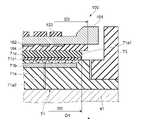
図3は、静電チャック71の構成を例示するための模式断面図である。
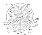
図4は、静電チャック71の模式平面図である。
図3に示すように、静電チャック71は、ベース41の上に設けられている。
静電チャック71は、例えば、誘電体71a、電極71b、および、フィルム71cを有する。FIG. 3 is a schematic cross-sectional view for illustrating the configuration of the
FIG. 4 is a schematic plan view of the
As shown in FIG. 3, the
The
誘電体71aは、中央領域の厚みが、中央領域を囲む周縁領域の厚みよりも厚い、段付き状を呈している。誘電体71aの周縁領域は、ネジなどの締結部材を用いてベース41に取り付けることができる。誘電体71aは、酸化アルミニウムなどのセラミックスから形成することができる。
図3および図4に示すように、誘電体71aの表面には、複数の溝71a1が設けられている。複数の溝71a1は、誘電体71aの表面に開口している。この場合、複数の溝71a1を複数の群に分け、1つの群に含まれる溝71a1同士を連通させることができる。例えば、図4に示すように、複数の溝71a1を3つの群71aa~71acに分けることができる。そして、群71aaに含まれる溝71a1同士を連通させ、群71abに含まれる溝71a1同士を連通させ、群71acに含まれる溝71a1同士を連通させることができる。The dielectric 71a has a stepped shape in which the thickness of the central region is thicker than the thickness of the peripheral region surrounding the central region. A peripheral region of the dielectric 71a can be attached to the base 41 using fastening members such as screws. The dielectric 71a can be made of ceramics such as aluminum oxide.
As shown in FIGS. 3 and 4, a plurality of grooves 71a1 are provided on the surface of the dielectric 71a. The plurality of grooves 71a1 are open on the surface of the dielectric 71a. In this case, the plurality of grooves 71a1 can be divided into a plurality of groups, and the grooves 71a1 included in one group can be communicated with each other. For example, as shown in FIG. 4, the plurality of grooves 71a1 can be divided into three groups 71aa-71ac. Then, the grooves 71a1 included in the group 71aa can be communicated with each other, the grooves 71a1 included in the group 71ab can be communicated with each other, and the grooves 71a1 included in the group 71ac can be communicated with each other.
また、誘電体71aには、複数の溝71a1に接続される複数の第1の孔71a2を設けることができる。複数の第1の孔71a2は、複数の溝71a1に後述する冷却ガスG1を供給する給気孔71a2aと、複数の溝71a1に供給された冷却ガスG1を排出する排気孔71a2bとに区分することができる。給気孔71a2aには、後述する冷却ガス供給部75を接続することができる。排気孔71a2bには、図示しない排気管などを接続することができる。例えば、1つの群71aa(71ab、71ac)に含まれる溝71a1に、少なくとも1つの給気孔71a2aと、排気孔71a2bとを接続することができる。 Also, the dielectric 71a can be provided with a plurality of first holes 71a2 connected to the plurality of grooves 71a1. The plurality of first holes 71a2 can be divided into air supply holes 71a2a that supply cooling gas G1, which will be described later, to the plurality of grooves 71a1, and exhaust holes 71a2b that discharge the cooling gas G1 supplied to the plurality of grooves 71a1. can. A cooling
給気孔71a2aを介して複数の溝71a1に供給された冷却ガスG1は、複数の溝71a1の内部を流れた後、排気孔71a2bを介して図示しない排気管などに排出される。すなわち、複数の溝71a1は、冷却ガス供給部75から供給された冷却ガスG1の流路となる。 The cooling gas G1 supplied to the plurality of grooves 71a1 through the air supply holes 71a2a flows inside the plurality of grooves 71a1, and then is discharged to an exhaust pipe (not shown) or the like through the exhaust holes 71a2b. That is, the plurality of
また、誘電体71aには、厚み方向に貫通する複数の孔71a3(第2の孔の一例に相当する)を設けることができる。複数の孔71a3のそれぞれには、リフトピン76を設けることができる(例えば、図6を参照)。
また、孔71a3に接続された溝71a1と、この溝71a1に接続された給気孔71a2aおよび排気孔71a2bを設けることができる。給気孔71a2aを介して溝71a1に供給された冷却ガスG1の一部は、溝71a1の内部を流れた後、孔71a3内に拡散する。そのため、孔71a3と対向する有機膜104の部分に冷却ガスG1の一部が直接触れる。したがって、冷却効率を向上させることができる。Further, the dielectric 71a can be provided with a plurality of holes 71a3 (corresponding to an example of second holes) penetrating in the thickness direction. A
Further, a groove 71a1 connected to the hole 71a3, and an air supply hole 71a2a and an exhaust hole 71a2b connected to the groove 71a1 can be provided. Part of the cooling gas G1 supplied to the groove 71a1 through the air supply hole 71a2a diffuses into the hole 71a3 after flowing through the inside of the groove 71a1. Therefore, part of the cooling gas G1 directly contacts the portion of the
電極71bは、板状を呈し、誘電体71aの内部に設けられている。電極71bは、単極型であってもよいし、双極型であってもよい。例えば、双極型の場合には、同一平面上に2つの電極71bを並べて設けることができる。電極71bは、例えば、タングステンやモリブデンなどの金属から形成することができる。 The
フィルム71cは、膜状を呈し、誘電体71aの表面に設けられている。フィルム71cは、複数の溝71a1の開口を覆っている。フィルム71cは、例えば、フッ素樹脂を含むことができる。また、フィルム71cと誘電体71aとの間に接合部71c1が設けられている。接合部71c1は、接着剤が硬化することで形成された層や、粘着テープなどとすることができる。 The
この場合、接合部71c1が溝71a1の内部に侵入すると冷却ガスの流通が阻害されるおそれがある。接合部71c1が粘着テープであれば、接合部71c1が溝71a1の内部に侵入するのを抑制することが容易となる。また、フィルム71cの貼り付け作業、およびフィルム71cの剥離作業が容易となる。 In this case, if the joint portion 71c1 enters the inside of the groove 71a1, there is a possibility that the circulation of the cooling gas is obstructed. If the joint portion 71c1 is an adhesive tape, it becomes easy to prevent the joint portion 71c1 from entering the groove 71a1. Moreover, the work of attaching the
また、接合部71c1の厚みとフィルム71cの厚みの合計が大きくなり過ぎると、基板100を吸着する力が弱くなったり、基板100の冷却が抑制されたりするおそれがある。そのため、接合部71c1の厚みとフィルム71cの厚みの合計は、100μm以下とすることが好ましい。 Also, if the sum of the thickness of the joint portion 71c1 and the thickness of the
また、フィルム71cの表面の凹凸が大きくなり過ぎると、フィルム71cと基板100(有機膜104)との間の隙間が大きくなる。そのため、基板100を吸着する力が弱くなったり、静電チャック71による基板100の冷却が抑制されたりする。 Further, if the unevenness of the surface of the
前述したように、接合部71c1の厚みとフィルム71cの厚みは薄いので、誘電体71aの表面の凹凸が、フィルム71cの表面に転写される。そのため、誘電体71aの表面の算術平均粗さRaは、0.3μm以下とすることが好ましい。この様にすれば、フィルム71cの表面の凹凸を小さくすることができる。 As described above, since the thickness of the joint portion 71c1 and the thickness of the
図5は、比較例に係る静電チャック171を例示するための模式断面図である。
静電チャック171には、誘電体71aおよび電極71bが設けられているが、フィルム71cは設けられていない。そのため、誘電体71aの表面に基板100の有機膜104が直接接触する。FIG. 5 is a schematic cross-sectional view for illustrating an
The
前述したように、誘電体71aは、酸化アルミニウムなどのセラミックスから形成されている。そのため、フィルム71cが無い静電チャック171に基板100が保持される場合、基板100と静電チャックの誘電体71aとが接触する。基板100と静電チャック171の誘電体71aとが接触することで、セラミックを含む微細な粒子が発生するおそれがある。また、プラズマによる熱によって、基板100と誘電体71aが膨張する。基板100と誘電体71aとは、膨張係数が異なるので、膨張した際に擦れるおそれもある。このため、誘電体71aの表面には、セラミックスなどを含む微細な粒子200が付着している場合がある。誘電体71aの表面に粒子200が付着した状態の静電チャック171に基板100が吸着されると、図5に示すように、誘電体71aの表面にある粒子200が有機膜104の内部に入り込む。 As described above, the dielectric 71a is made of ceramics such as aluminum oxide. Therefore, when the
また、誘電体71aの溝71a1は、一般的に切削して形成される。このため、バリが溝71a1に形成されているおそれもある。溝71a1には冷却ガスG1が流れるので、プラズマ処理中にバリが溝71a1から剥離し、粒子200となるおそれがある。また、後述の冷却ガス供給部75は、不図示のフィルタを介して冷却ガスG1を供給している。しかし、フィルタから漏れてしまった粒子200や、フィルタを経た後、溝71a1までの経路の間に存在していた粒子200が冷却ガスG1に含まれるおそれもある。そのため、フィルム71cが無い静電チャック171では、溝71a1の内部にある粒子200が、冷却ガスG1により有機膜104の内部に入り込む場合がある。 Further, the groove 71a1 of the dielectric 71a is generally formed by cutting. Therefore, burrs may be formed in the grooves 71a1. Since the cooling gas G1 flows through the grooves 71a1, there is a possibility that burrs may be separated from the grooves 71a1 and become
また、誘電体71aには、リフトピン76を設けるための孔71a3が設けられる場合がある。冷却ガスが孔71a3に供給される場合には、孔71a3の内壁にある粒子200が、冷却ガスにより有機膜104の内部に入り込む場合がある。 Further, the dielectric 71a may be provided with a hole 71a3 for providing the
この場合、粒子200の粒子径が、デバイス102の端部と有機膜104の表面との間の距離よりも大きいと、有機膜104の内部に入り込んだ粒子200がデバイス102に到達する。そのため、デバイス102が損傷するおそれがある。 In this case, if the particle diameter of the
図6は、フィルム71cの作用を例示するための模式断面図である。
前述したように、フィルム71cは、誘電体71aの表面に設けられている。そのため、図6に示すように、誘電体71aの表面に粒子200が付着していたとしても、フィルム71cにより、粒子200が有機膜104の内部に入り込むのを抑制することができる。FIG. 6 is a schematic cross-sectional view for illustrating the action of the
As described above, the
また、前述したように、フィルム71cは、複数の溝71a1の開口を覆っている。そのため、溝71a1の内壁にある粒子200が、冷却ガスにより有機膜104の内部に入り込むのを抑制することができる。 Moreover, as described above, the
図7は、フィルム71cの効果を例示するためのグラフ図である。
図7中の「A1」、「A2」は、比較例に係る静電チャック171において、有機膜104の表面に付着した粒子200の数を表している。すなわち、フィルム71cが設けられていない場合に有機膜104の表面に付着した粒子200の数を表している。「A2」は、粒子200の粒子径が5μm以上の場合である。すなわち、「A2」は、前述したデバイス102の損傷が発生し得る程度の大きさを有する粒子200の数を表している。
「A1」は、粒子200の粒子径が0.3μ以上、5μm未満の場合である。すなわち、「A1」は、デバイス102の損傷が発生し得る程度の大きさを有する粒子200を除いたほぼ全ての大きさの粒子200の数を表している。FIG. 7 is a graph diagram illustrating the effect of the
"A1" and "A2" in FIG. 7 represent the number of
“A1” is the case where the particle diameter of the
「B1」は、本実施の形態に係る静電チャック71において、有機膜104の表面に付着した粒子200の数を表している。すなわち、フィルム71cが設けられている場合に有機膜104の表面に付着した粒子200の数を表している。「B1」は粒子200の粒子径が0.3μm以上、5μm未満の場合である。すなわち、「B1」は、デバイス102の損傷が発生し得る程度の大きさを有する粒子200を除いたほぼ全ての大きさの粒子200の数を表している。 "B1" represents the number of
図7から分かるように、フィルム71cにより、複数の溝71a1の開口が覆われていれば、有機膜104の表面に付着するほぼ全ての大きさの粒子200の数を減らすことができる。つまり、有機膜104に付着する粒子200を抑制することができる。また、デバイス102に損傷が発生し得る程度の大きさを有する粒子200が、有機膜104の表面に付着するのを無くすことができた。つまり、デバイス102の損傷が発生し得る5μm以上の大きさを有する粒子の発生を防止することができる。 As can be seen from FIG. 7, if the openings of the plurality of grooves 71a1 are covered with the
本発明者らは、確認のため、アルミニウム製の基板の表面に有機膜104を形成し、粒子200による圧痕が基板の表面に発生するか否かの実験を行った。なお、圧痕は、平面寸法が、5μm×5μm以上の傷や窪みなどとしている。 For confirmation, the inventors formed the
静電チャック171の場合(フィルム71cが設けられていない場合)には、67個の圧痕が発生した。
静電チャック71の場合(フィルム71cが設けられている場合)には、圧痕の発生はなかった。このことは、フィルム71cを静電チャック71の表面に設ければ、デバイス102に損傷が発生するのを抑制できることを意味する。In the case of the electrostatic chuck 171 (without the
In the case of the electrostatic chuck 71 (when the
一方で、プラズマ処理を実施した後、静電チャック71から基板100を分離すると、基板100の有機膜104の一部が静電チャック71の表面(フィルム71c上)に残留してしまうことが判明した。このときのフィルム71cは、ポリイミドで形成されていた。 On the other hand, it was found that when the
誘電体71aの表面に設けられたフィルム71cに有機膜104の一部が付着すると、静電チャック71と基板100との密着性が阻害され、静電チャック71による基板100の冷却が抑制されたり、静電チャック71の吸着力が弱くなったりする。 If a part of the
本発明者らは、有機膜104がガラス基板およびシートのように接着層を有しないことが原因であると考えた。つまり、本発明者らは、有機膜104の、デバイス102およびデバイス面101bとの接着力が有機膜104のフィルム71cの表面との付着力よりも弱いためだと考えた。 The inventors considered that the reason for this is that the
本実施形態の場合、フィルム71cは、フッ素樹脂を含んでいるため、有機膜104の材料が付着し難い。また、レジストマスク103の除去を行った際にプラズマによるフィルム71cの分解や変質が生じ難くなる。 In the case of the present embodiment, the
また、後述するマスクリング73と基板100との隙間からエッチャントが侵入することがある。この場合、図3に示すように、誘電体71aの、その表面に平行な方向の寸法をD1(mm)、フィルム71cの、その表面に平行な方向の寸法をD2(mm)とすると、「D2(mm)<D1(mm)」とすることが好ましい。この様にすれば、接合部71c1の周端面が、誘電体71aの周端面よりも誘電体71aの中心側に設けられる。したがって、マスクリング73と基板100との間の隙間から侵入したエッチャントが接合部71c1の周端近傍に到達し難くなる。そのため、接合部71c1の周端近傍が分解されて、フィルム71cの周端近傍が誘電体71aの表面から剥離するのを抑制することができる。本発明者らの得た知見によれば、誘電体71aの周端面とフィルム71cの周端面との間の距離をL(mm)とすると、「0.5mm≦L≦5mm」とすることが好ましい。この様にすれば、フィルム71cの周端近傍が誘電体71aの表面から剥離するのを効果的に抑制することができる。なお、エッチャントとは、プラズマPにより励起、活性化されたガスGから生成されるイオン、ラジカル等の活性種のことである。 Also, the etchant may enter through a gap between the
ここで、有機膜104は、除去対象であるレジストマスク103と同質である。このため、レジストマスク103の除去を行った際に、有機膜104の露出部分(例えば、有機膜104の周端面)がマスクリング73と基板100との間の隙間から侵入したエッチャントにより分解される場合がある。分解された有機膜104の材料がフィルム71cの表面に付着すると、付着した有機膜104の材料が熱などにより変質して硬くなる場合がある。また、基板100の処理枚数が多くなるに従い、付着量が経時的に増加する場合がある。静電チャック71(フィルム71c)の表面に、硬さの硬い付着物や、サイズの大きい付着物があると、基板100を静電チャック71に載置した際に、付着物と基板100が干渉するおそれがある。付着物と基板100が干渉すると、基板100が損傷したり、基板100を吸着する力が弱くなったり、基板100の温度の面内分布にばらつきが生じたりするおそれがある。 Here, the
そこで、本実施の形態に係る静電チャック71においては、有機膜104の、その表面に平行な方向の寸法をD3とした場合に、「D2(mm)<D3(mm)」となるようにしている。この様にすれば、基板100を吸着した際に、フィルム71cが有機膜104により覆われるので、有機膜104の周端近傍が分解されたとしても、有機膜104の材料がフィルム71cの表面に付着するのを抑制することができる。そのため、付着した有機膜104の材料により、基板100が損傷したり、基板100を吸着する力が弱くなったり、基板100の温度の面内分布にばらつきが生じたりするのを抑制することができる。 Therefore, in the
前述の通り、セラミックなどを含む粒子200は、静電チャックと基板100との接触により発生する。しかし、前述の通り、誘電体71aの表面の凹凸を小さくするために、誘電体71aの表面は、研磨される。このため、セラミックなどを含む粒子200は、誘電体71aを形成する際にも発生していると考えられる。誘電体71aを形成する際に発生したセラミックなどを含む粒子200は、誘電体71aの表面に付着するものと考えられる。誘電体71aの形成中に付着するセラミックなどを含む粒子200は、通常の洗浄では取り切れず、その一部が誘電体71aに付着したままとなる。 As described above,
セラミックなどを含む粒子200が誘電体71aに付着している問題に対して、本発明者らは、フィルム71cで誘電体71aの表面および溝71a1を覆うことによって対応した。
この場合、誘電体71aの周端近傍をフィルム71cで覆っていない状態で、「D2(mm)<D3(mm)」とすると、セラミックなどを含む粒子200が有機膜104の周端近傍に付着するおそれがある。To solve the problem that the
In this case, if "D2 (mm)<D3 (mm)" is satisfied in a state in which the vicinity of the peripheral edge of the dielectric 71a is not covered with the
本実施形態では、有機膜104の周端近傍は、静電チャック71と接触することがない。そのため、有機膜104の周端近傍に5μm以上の粒子200が付着していても、5μm以上の粒子200が有機膜104の内部に入り込むことが無いように思われる。しかし、プラズマ処理後の基板100の搬送中、および次工程で基板100の裏面101aへ処理を実施する場合、有機膜104は、搬送アーム、あるいは別装置の静電チャックに接触するおそれがある。つまり、デバイス102の損傷が発生し得る5μm以上の粒子200が、有機膜104の周端近傍に付着していると、デバイスに損傷を与えるおそれがある。しかし、図7に示したように、本実施形態では、デバイス102の損傷が発生し得る5μm以上の粒子200が有機膜104に付着することが抑制できている。 In this embodiment, the vicinity of the peripheral edge of the
誘電体71aの周端近傍をフィルム71cで覆わなくとも、デバイス102の損傷が発生し得る5μm以上の粒子200が有機膜104に付着しないメカニズムは必ずしも明らかではない。しかし、以下の様に考えることができる。
誘電体71aの表面にフィルム71cを貼り付けていることで、誘電体71aの周端近傍に付着しているセラミックなどを含む粒子200と基板100の有機膜104との間に距離が生じる。そのため、有機膜104へ粒子200が付着することを抑制できていると考えられる。The mechanism by which the
By attaching the
次に、図2に戻って、載置部7に設けられた他の要素について説明する。
図2に示すように、絶縁リング72は、筒状を呈し、チャンバ2の底部に設けられている。絶縁リング72は、ベース41の側面を覆っている。絶縁リング72は、例えば、石英などの誘電体材料から形成することができる。Next, referring back to FIG. 2, other elements provided on the
As shown in FIG. 2 , the insulating
マスクリング73は、筒状を呈し、静電チャック71の誘電体71aの周縁領域に設けられている。マスクリング73は、静電チャック71の中央領域を囲んでいる。マスクリング73をこのように配置することで、誘電体71aの周縁近傍がエッチャントに曝されることを防ぐことができる。そのため、誘電体71aの周縁領域に設けられている、前述した締結部材がエッチャントにより損傷するのを抑制することができる。 The
マスクリング73は、例えば、石英などの誘電体材料から形成することができる。
また、マスクリング73が設けられていれば、レジストマスク103の除去を行う際に、エッチャントが有機膜104の周端面に到達するのを抑制することができる。そのため、有機膜104の周端面が分解されることで発生する有機膜104の材料が静電チャック71の表面に付着するのを抑制することができる。
Moreover, if the
電源ユニット74は、例えば、直流電源74a、および切り替えスイッチ74bを有する。直流電源74aは、静電チャック71の電極71bと電気的に接続されている。直流電源74aにより、電極71bに電圧が印加されると、電極71bの基板100側の面に電荷が発生する。そのため、電極71bと基板100との間に静電力が発生し、発生した静電力により、基板100が静電チャック71に吸着される。 The
切り替えスイッチ74bは、直流電源74aと、静電チャック71の電極71bとの間に電気的に接続され、基板100の吸着と、吸着の解除とを切り替える。 The
冷却ガス供給部75は、誘電体71aに設けられた給気孔71a2aを介して溝71a1に冷却ガスG1を供給する。すなわち、冷却ガス供給部75は、フィルム71cにより開口が覆われた複数の溝71a1の内部に冷却ガスを供給する。 The cooling
冷却ガス供給部75は、例えば、ガス源75a、ガスコントローラ75b、および開閉バルブ75cを有する。ガス源75aは、例えば、冷却ガスG1を収納した高圧ボンベなどとすることができる。また、ガス源75aは、例えば、工場配管などであってもよい。冷却ガスG1は、例えば、ヘリウムガスなどとすることができる。 The cooling
ガスコントローラ75bは、ガス源75aと静電チャック71との間に設けることができる。ガスコントローラ75bは、ガス源75aから供給された冷却ガスG1の流量および圧力の少なくともいずれかを制御する。ガスコントローラ75bは、例えば、MFCなどとすることができる。 A
例えば、ガスコントローラ75bは、レジストマスク103の除去を行う際に、基板100の表面温度が80℃以下となるように、冷却ガスの流量および圧力の少なくともいずれかを制御することができる。例えば、ガスコントローラ75bは、静電チャック71の温度が45℃以下となるようにすることで、基板100の表面温度が80℃以下となるようにすることができる。例えば、ガスコントローラ75bは、図示しない圧力計による、フィルム71cと、複数の溝71a1と、により画された空間の圧力の検出値が、400Pa~2000Paとなるように、冷却ガスG1の供給流量を制御することで、基板100の表面温度が80℃以下となるようにすることができる。 For example, the
開閉バルブ75cは、ガスコントローラ75bと静電チャック71との間に設けることができる。開閉バルブ75cは、冷却ガスG1の供給の開始と供給の停止を制御する。開閉バルブ75cは、例えば、2ポート電磁弁などとすることができる。なお、開閉バルブ75cの機能をガスコントローラ75bに持たせることもできる。 The open/
ここで、前述したように、フィルム71cは、複数の溝71a1の開口を覆っている。そのため、複数の溝71a1に供給された冷却ガスG1は、フィルム71cを介して、基板100の冷却を行う。この場合、冷却効果を向上させるために、冷却ガスG1の温度は常温以下(例えば、25℃以下)とすることが好ましい。 Here, as described above, the
フィルム71cと、複数の溝71a1と、により画された空間に冷却ガスG1を供給すれば、フィルム71cに冷却ガスG1が直接接触する。そのため、冷却ガスG1により、誘電体71aを介してフィルム71cを冷却するよりも伝熱効率が良い。 If the cooling gas G1 is supplied to the space defined by the
例えば、冷却ガス供給部75は、供給する冷却ガスG1を冷却する冷却器75dをさらに有することもできる。冷却器75dは、例えば、冷却ガスG1の温度が-20℃以下となるように冷却ガスG1を冷却する熱交換器などとすることができる。なお、液化された冷却ガスG1を気化させて冷却ガスG1としてもよい。この様にすれば、冷却器75dを設けなくても、-20℃以下の冷却ガスG1を静電チャック71に供給することができる。 For example, the cooling
また、本実施の形態では、給気孔71a2aと排気孔71a2bとに分けることができる。このようにすることで、デバイス102にダメージを与えるおそれのある粒径の粒子200の発生を防止しつつ、フィルム71cと、複数の溝71a1と、により画された空間に、冷却ガスG1の流れを形成することができる。このため、冷却効率が向上する。 Further, in the present embodiment, it can be divided into the air supply hole 71a2a and the air exhaust hole 71a2b. By doing so, while preventing generation of
また、本実施形態のプラズマ処理装置1は、ベース101の裏面101aに凹部101a1を有する基板100にプラズマ処理することに特に優れている。
ベース101の厚みが全体的に薄い基板100の場合、基板100は、剛性が低いので、撓んでしまう。そのため、厚みのあるガラス基板やシートを使用して剛性を補っている。Moreover, the
In the case of the
本実施形態の基板100は、ベース101の外周部が厚い。そのため、本実施形態の基板100は、ベース101の厚みが全体的に薄い基板100と比べて、剛性が向上する。したがって、本実施形態の基板100は、ガラス基板やシートを使用して剛性を補う必要がない。そのため、有機膜104は、デバイス102を保護できる厚みがあればよい。つまり、本実施形態の基板100は、有機膜104の厚みをガラス基板やシートの厚みよりも薄くすることができる。 The
有機膜104の厚みは、ガラス基板またはシートと比べて、とても薄い。そのため、静電チャック71が本実施形態の基板100を吸着する力は、ガラス基板またはシートで保護された基板100を吸着する場合と比べて大きい。したがって、フィルム71cと、複数の溝71a1と、により画された空間の圧力を、ガラス基板またはシートで保護された基板100を吸着する場合の圧力よりも大きくしたとしても、本実施形態の基板100が静電チャック71から分離されることは無い。つまり、フィルム71cと、複数の溝71a1と、により画された空間に従来よりも高い圧力の冷却ガスG1を供給したとしても、フィルム71cが冷却ガスG1の圧力により膨張することは無い。前述の通り、フィルム71cと、複数の溝71a1と、により画された空間に従来よりも圧力の高い状態で冷却ガスG1を供給することができる。そのため、本実施形態の基板100の冷却効率は、ガラス基板またはシートで保護された基板100の冷却効率よりも良い。 The thickness of the
また、本実施の形態では、有機膜104の厚みを3μm以上、10μm以下とすることができる。有機膜104の厚みを上記の範囲とすることで、上記のように、従来よりも圧力の高い状態で冷却ガスG1を供給することができる。そのため、ガラス基板またはシートで保護された基板100の冷却効率よりも冷却効率が良い。また、デバイス102を有機膜で保護された基板100は、有機膜104の厚みが薄い。そのため、ベース101への熱伝導がよくなる。したがって、デバイス102を有機膜104で保護された基板100は、ガラス基板またはシートで保護された基板100よりも冷却効率が良くなる。 Further, in this embodiment, the thickness of the
以上、実施の形態について例示をした。しかし、本発明はこれらの記述に限定されるものではない。
前述の実施の形態に関して、当業者が適宜、構成要素の追加、削除若しくは設計変更を行ったもの、または、工程の追加、省略若しくは条件変更を行ったものも、本発明の特徴を備えている限り、本発明の範囲に包含される。
また、前述した各実施の形態が備える各要素は、可能な限りにおいて組み合わせることができ、これらを組み合わせたものも本発明の特徴を含む限り本発明の範囲に包含される。The embodiments have been illustrated above. However, the invention is not limited to these descriptions.
With respect to the above-described embodiments, those in which a person skilled in the art appropriately adds, deletes, or modifies the design of components, or adds, omits, or modifies the conditions of steps, also has the features of the present invention. as long as it is within the scope of the present invention.
Moreover, each element provided in each of the above-described embodiments can be combined as much as possible, and a combination thereof is also included in the scope of the present invention as long as it includes the features of the present invention.
例えば、プラズマ処理の例として、レジストマスク103の除去を記載したが、これに限らない。例えば、基板100のベース101の裏面101aをエッチングする処理や、ベース101の裏面101aに金属膜や絶縁膜を形成する処理もプラズマ処理に含まれる。
例えば、フィルム71cの、給気孔71a2aと対向する部分に開口を設けるようにしてもよい。このようにすることで、基板100の冷却効率が向上する。
例えば、第1の孔71a2を給気孔71a2aと排気孔71a2bと区別したが、区別することなく使用してもよい。例えば、プラズマ処理中は、第1の孔71a2からガスGを供給し続け、プラズマ処理が終了したら、第1の孔71a2から排気するようにしてもよい。For example, although removal of the resist
For example, an opening may be provided in a portion of the
For example, although the first hole 71a2 is distinguished from the air supply hole 71a2a and the air exhaust hole 71a2b, it may be used without distinction. For example, the gas G may be continuously supplied from the first hole 71a2 during the plasma processing, and exhausted from the first hole 71a2 after the plasma processing is finished.
1 プラズマ処理装置、2 チャンバ、3 電源ユニット、4 電源ユニット、5 減圧部、6 ガス供給部、7 載置部、71 静電チャック、71a 誘電体、71a1 溝、71b 電極、71c フィルム、71c1 接合部、75 冷却ガス供給部、100 基板、101 ベース、102 デバイス、103 レジストマスク、104 有機膜 1 plasma processing apparatus, 2 chamber, 3 power supply unit, 4 power supply unit, 5 decompression unit, 6 gas supply unit, 7 mounting unit, 71 electrostatic chuck, 71a dielectric, 71a1 groove, 71b electrode, 71c film, 71c1
Claims (6)
Translated fromJapanese前記基板の、前記有機膜が形成された側が載置される静電チャックを備え、
前記静電チャックは、
表面に開口する複数の溝を有する誘電体と、
前記誘電体の内部に設けられた電極と、
前記誘電体の前記表面に設けられ、前記複数の溝の開口を覆い、フッ素樹脂を含むフィルムと、
前記フィルムと、前記誘電体と、の間に設けられた接合部と、
を有し、
前記誘電体の、前記表面に平行な方向の寸法をD1(mm)、前記フィルムの、表面に平行な方向の寸法をD2(mm)とした場合に、以下の式を満足するプラズマ処理装置。
D2(mm)<D1(mm)a base, a plurality of devices provided on one surface of the base, an organic film provided on one surface of the base to cover the plurality of devices, and a resist mask provided on the other surface of the base and a plasma processing apparatus for processing a substrate having
An electrostatic chuck on which the side of the substrate on which the organic film is formed is placed,
The electrostatic chuck is
a dielectric having a plurality of grooves open to its surface;
an electrode provided inside the dielectric;
a film provided on the surface of the dielectric, covering openings of the plurality of grooves, and containing a fluororesin;
a joint provided between the film and the dielectric;
has
A plasma processing apparatus satisfying the following formula, where D1 (mm) is the dimension of the dielectric in the direction parallel to the surface, and D2 (mm) is the dimension of the film in the direction parallel to the surface.
D2 (mm) < D1 (mm)
D2(mm)<D3(mm)3. The plasma processing apparatus according to claim 1, wherein the following expression is satisfied, where D3 is the dimension of the organic film in the direction parallel to the surface.
D2 (mm) < D3 (mm)
0.5mm≦L≦5mm4. The plasma processing apparatus according to any one of claims 1 to 3, wherein the distance between the peripheral end surface of the dielectric and the peripheral end surface of the film satisfies the following equation.
0.5mm≤L≤5mm
Priority Applications (2)
| Application Number | Priority Date | Filing Date | Title |
|---|---|---|---|
| CN202110729723.5ACN113948360B (en) | 2020-07-15 | 2021-06-29 | Plasma processing apparatus |
| TW110124573ATWI794864B (en) | 2020-07-15 | 2021-07-05 | Plasma treatment device |
Applications Claiming Priority (2)
| Application Number | Priority Date | Filing Date | Title |
|---|---|---|---|
| JP2020121434 | 2020-07-15 | ||
| JP2020121434 | 2020-07-15 |
Publications (2)
| Publication Number | Publication Date |
|---|---|
| JP2022019549A JP2022019549A (en) | 2022-01-27 |
| JP7146017B2true JP7146017B2 (en) | 2022-10-03 |
Family
ID=80203715
Family Applications (1)
| Application Number | Title | Priority Date | Filing Date |
|---|---|---|---|
| JP2021079052AActiveJP7146017B2 (en) | 2020-07-15 | 2021-05-07 | Plasma processing equipment |
Country Status (1)
| Country | Link |
|---|---|
| JP (1) | JP7146017B2 (en) |
Citations (8)
| Publication number | Priority date | Publication date | Assignee | Title |
|---|---|---|---|---|
| JP2002324834A (en) | 2002-04-03 | 2002-11-08 | Tomoegawa Paper Co Ltd | Electrostatic chuck device, laminated sheet for electrostatic chuck, and adhesive for electrostatic chuck |
| JP2004128128A (en) | 2002-10-01 | 2004-04-22 | Matsushita Electric Ind Co Ltd | Plasma processing method and apparatus |
| JP2004140056A (en) | 2002-10-16 | 2004-05-13 | Nok Corp | Electrostatic chuck |
| JP2004172365A (en) | 2002-11-20 | 2004-06-17 | Matsushita Electric Ind Co Ltd | Method for manufacturing semiconductor device |
| JP2004273771A (en) | 2003-03-10 | 2004-09-30 | Fuji Electric Device Technology Co Ltd | Method for manufacturing semiconductor device |
| JP2006019374A (en) | 2004-06-30 | 2006-01-19 | Ulvac Japan Ltd | Vacuum processing method |
| JP2015138807A (en) | 2014-01-20 | 2015-07-30 | 株式会社ディスコ | Plasma etching equipment |
| JP2016530726A (en) | 2013-08-29 | 2016-09-29 | プラズマ − サーム、エルエルシー | Method and apparatus for plasma dicing a semiconductor wafer |
Family Cites Families (1)
| Publication number | Priority date | Publication date | Assignee | Title |
|---|---|---|---|---|
| EP0692156A1 (en)* | 1994-01-31 | 1996-01-17 | Applied Materials, Inc. | Electrostatic chuck with conformal insulator film |
- 2021
- 2021-05-07JPJP2021079052Apatent/JP7146017B2/enactiveActive
Patent Citations (8)
| Publication number | Priority date | Publication date | Assignee | Title |
|---|---|---|---|---|
| JP2002324834A (en) | 2002-04-03 | 2002-11-08 | Tomoegawa Paper Co Ltd | Electrostatic chuck device, laminated sheet for electrostatic chuck, and adhesive for electrostatic chuck |
| JP2004128128A (en) | 2002-10-01 | 2004-04-22 | Matsushita Electric Ind Co Ltd | Plasma processing method and apparatus |
| JP2004140056A (en) | 2002-10-16 | 2004-05-13 | Nok Corp | Electrostatic chuck |
| JP2004172365A (en) | 2002-11-20 | 2004-06-17 | Matsushita Electric Ind Co Ltd | Method for manufacturing semiconductor device |
| JP2004273771A (en) | 2003-03-10 | 2004-09-30 | Fuji Electric Device Technology Co Ltd | Method for manufacturing semiconductor device |
| JP2006019374A (en) | 2004-06-30 | 2006-01-19 | Ulvac Japan Ltd | Vacuum processing method |
| JP2016530726A (en) | 2013-08-29 | 2016-09-29 | プラズマ − サーム、エルエルシー | Method and apparatus for plasma dicing a semiconductor wafer |
| JP2015138807A (en) | 2014-01-20 | 2015-07-30 | 株式会社ディスコ | Plasma etching equipment |
Also Published As
| Publication number | Publication date |
|---|---|
| JP2022019549A (en) | 2022-01-27 |
Similar Documents
| Publication | Publication Date | Title |
|---|---|---|
| US11935727B2 (en) | Substrate processing method | |
| JP5719599B2 (en) | Substrate processing equipment | |
| JP3971603B2 (en) | Insulating film etching apparatus and insulating film etching method | |
| US8449785B2 (en) | Substrate processing method | |
| JP5281811B2 (en) | Annular parts for plasma processing, plasma processing apparatus, and outer annular member | |
| US8216485B2 (en) | Plasma etching method, plasma etching apparatus, control program and computer-readable storage medium | |
| KR102569911B1 (en) | Focus ring and substrate processing apparatus | |
| WO2002007212A1 (en) | Holding device for treated body | |
| JP7433164B2 (en) | Substrate processing system | |
| JP5503503B2 (en) | Plasma processing equipment | |
| US20120037314A1 (en) | Substrate processing apparatus and side wall component | |
| JP4469364B2 (en) | Insulating film etching equipment | |
| US20070284337A1 (en) | Etching method, plasma processing system and storage medium | |
| US10991551B2 (en) | Cleaning method and plasma processing apparatus | |
| JP4656364B2 (en) | Plasma processing method | |
| JP2020077654A (en) | Mounting table and substrate processing apparatus | |
| JP7146017B2 (en) | Plasma processing equipment | |
| JP7341043B2 (en) | Substrate processing method and substrate processing apparatus | |
| JP4129152B2 (en) | Substrate mounting member and substrate processing apparatus using the same | |
| JP7646308B2 (en) | Plasma Processing Equipment | |
| TWI794864B (en) | Plasma treatment device | |
| KR20210046150A (en) | System and method for treating substrate | |
| JP4616605B2 (en) | Plasma processing method, plasma processing apparatus, and storage medium | |
| US20240071783A1 (en) | Apparatus for treating substrate | |
| JP2010080990A (en) | Insulation film etching apparatus |
Legal Events
| Date | Code | Title | Description |
|---|---|---|---|
| A621 | Written request for application examination | Free format text:JAPANESE INTERMEDIATE CODE: A621 Effective date:20210819 | |
| A977 | Report on retrieval | Free format text:JAPANESE INTERMEDIATE CODE: A971007 Effective date:20220810 | |
| TRDD | Decision of grant or rejection written | ||
| A01 | Written decision to grant a patent or to grant a registration (utility model) | Free format text:JAPANESE INTERMEDIATE CODE: A01 Effective date:20220826 | |
| A61 | First payment of annual fees (during grant procedure) | Free format text:JAPANESE INTERMEDIATE CODE: A61 Effective date:20220920 | |
| R150 | Certificate of patent or registration of utility model | Ref document number:7146017 Country of ref document:JP Free format text:JAPANESE INTERMEDIATE CODE: R150 |