JP7145229B2 - Manufacturing method of planar coil assembly and sensor head provided with the same - Google Patents
Manufacturing method of planar coil assembly and sensor head provided with the sameDownload PDFInfo
- Publication number
- JP7145229B2 JP7145229B2JP2020555805AJP2020555805AJP7145229B2JP 7145229 B2JP7145229 B2JP 7145229B2JP 2020555805 AJP2020555805 AJP 2020555805AJP 2020555805 AJP2020555805 AJP 2020555805AJP 7145229 B2JP7145229 B2JP 7145229B2
- Authority
- JP
- Japan
- Prior art keywords
- coil
- planar
- manufacturing
- planar coil
- coils
- Prior art date
- Legal status (The legal status is an assumption and is not a legal conclusion. Google has not performed a legal analysis and makes no representation as to the accuracy of the status listed.)
- Active
Links
Images


Classifications
- H—ELECTRICITY
- H01—ELECTRIC ELEMENTS
- H01F—MAGNETS; INDUCTANCES; TRANSFORMERS; SELECTION OF MATERIALS FOR THEIR MAGNETIC PROPERTIES
- H01F41/00—Apparatus or processes specially adapted for manufacturing or assembling magnets, inductances or transformers; Apparatus or processes specially adapted for manufacturing materials characterised by their magnetic properties
- H01F41/02—Apparatus or processes specially adapted for manufacturing or assembling magnets, inductances or transformers; Apparatus or processes specially adapted for manufacturing materials characterised by their magnetic properties for manufacturing cores, coils, or magnets
- H01F41/04—Apparatus or processes specially adapted for manufacturing or assembling magnets, inductances or transformers; Apparatus or processes specially adapted for manufacturing materials characterised by their magnetic properties for manufacturing cores, coils, or magnets for manufacturing coils
- H01F41/041—Printed circuit coils
- H—ELECTRICITY
- H01—ELECTRIC ELEMENTS
- H01F—MAGNETS; INDUCTANCES; TRANSFORMERS; SELECTION OF MATERIALS FOR THEIR MAGNETIC PROPERTIES
- H01F5/00—Coils
- H01F5/003—Printed circuit coils
- G—PHYSICS
- G01—MEASURING; TESTING
- G01L—MEASURING FORCE, STRESS, TORQUE, WORK, MECHANICAL POWER, MECHANICAL EFFICIENCY, OR FLUID PRESSURE
- G01L3/00—Measuring torque, work, mechanical power, or mechanical efficiency, in general
- G01L3/02—Rotary-transmission dynamometers
- G01L3/04—Rotary-transmission dynamometers wherein the torque-transmitting element comprises a torsionally-flexible shaft
- G01L3/10—Rotary-transmission dynamometers wherein the torque-transmitting element comprises a torsionally-flexible shaft involving electric or magnetic means for indicating
- Y—GENERAL TAGGING OF NEW TECHNOLOGICAL DEVELOPMENTS; GENERAL TAGGING OF CROSS-SECTIONAL TECHNOLOGIES SPANNING OVER SEVERAL SECTIONS OF THE IPC; TECHNICAL SUBJECTS COVERED BY FORMER USPC CROSS-REFERENCE ART COLLECTIONS [XRACs] AND DIGESTS
- Y10—TECHNICAL SUBJECTS COVERED BY FORMER USPC
- Y10T—TECHNICAL SUBJECTS COVERED BY FORMER US CLASSIFICATION
- Y10T29/00—Metal working
- Y10T29/49—Method of mechanical manufacture
- Y10T29/49002—Electrical device making
Landscapes
- Engineering & Computer Science (AREA)
- Power Engineering (AREA)
- Manufacturing & Machinery (AREA)
- Physics & Mathematics (AREA)
- General Physics & Mathematics (AREA)
- Coils Or Transformers For Communication (AREA)
- Manufacturing Cores, Coils, And Magnets (AREA)
- Magnetic Heads (AREA)
Description
Translated fromJapanese本発明は、複数の平面コイルユニットが積層されて配置された平面コイルアセンブリを製造する方法に関する。本発明はまた、平面コイルアセンブリを製造する方法を実施することによって、トルクセンサー用または応力センサー用のセンサーヘッドを製造するプロセスに関する。最後に、本発明は、そのような方法によって得られるセンサーヘッドに関する。 The present invention relates to a method of manufacturing a planar coil assembly in which a plurality of planar coil units are stacked and arranged. The invention also relates to a process for manufacturing a sensor head for a torque sensor or a stress sensor by implementing the method for manufacturing a planar coil assembly. Finally, the invention relates to a sensor head obtained by such a method.
特に、本発明は、磁場の変化を捉えることによってシャフトのトルクを測定することができる、トルクトランスデューサないしはトルクセンサーのためのセンサーヘッドについての特に有利な製造に関する。磁場の変化に基づいてシャフトのトルクを検出する、このようなトルクセンサー、およびその科学的根拠は、下記の文献D1~D9(非特許文献1、及び特許文献1~8)に記載されている。 In particular, the invention relates to a particularly advantageous manufacture of a sensor head for a torque transducer or torque sensor capable of measuring the torque of a shaft by picking up changes in the magnetic field. Such torque sensors that detect shaft torque based on changes in the magnetic field, and the scientific basis thereof, are described in the following documents D1-D9 (Non-Patent Document 1 and Patent Documents 1-8). .
特に、D4(DE 30 31 997 A1;特許文献3)に記載されているトルクトランスデューサの設計は、シャフトやその他の測定ポイントのトルクを測定するのに特に効果的であることが証明されています。 In particular, the torque transducer design described in D4 (
このような応力センサーまたはトルクセンサーのためのセンサーヘッドを製造するのに特に有利な方法は、下記の文献D10(特許文献9)に記述され示されている。 A particularly advantageous method of manufacturing a sensor head for such a stress sensor or torque sensor is described and shown in document D10 below.
この文献によると、磁場を生成するための発生器コイル、ならびに磁場の変化を測定するための測定コイルは、積層されて配置され、ビアホールないしはスルーホールを通じて互いに接続された複数の平面コイルによって形成される。したがって、文献D10(特許文献9)は、n個の重ね合わされた平面コイルユニットを含む平面コイルアセンブリを製造するための方法を記載している。ここで、nは、1より大きい自然数であり、この方法は、ステップa)及びb)を含む。 According to this document, the generator coil for generating the magnetic field as well as the measuring coil for measuring changes in the magnetic field are formed by a plurality of planar coils arranged in a stack and connected to each other through via holes or through holes. be. Document D10 therefore describes a method for manufacturing a planar coil assembly comprising n superimposed planar coil units. where n is a natural number greater than 1 and the method includes steps a) and b).
a)コンピュータを用いて、電気絶縁材料から作製された厚みdi,IMの絶縁材料層の上に、導電体から作製された、平面コイル厚さdi,PSを有する少なくとも1つの平面コイルを製造することにより、i番目の平面コイルユニットを作成する。ここで、iは1からnに等しい。a) using a computer to form at least one planar coil made of an electrical conductor and having a planar coil thickness di,PS on a layer of insulating material of thickness di,IM made of an electrically insulating material; Manufacturing creates the i-th planar coil unit. where i is equal to 1 to n.
b)平面コイル同士の間に絶縁材料層を挟み込むようにして、平面コイルユニットを積層して配置する。 b) The planar coil units are stacked such that an insulating material layer is sandwiched between the planar coils.
平面コイルアセンブリ―を作成する方法は、下記の文献D11~13(特許文献10~12)からも知られている。 Methods for making planar coil assemblies are also known from documents D11-13 listed below.
本発明の特に好ましい実施形態は、可撓性プリント回路基板の使用法およびそれらの用途を提供する。このことについては、特に、文献D14(特許文献13)が引用・参照される。 Particularly preferred embodiments of the present invention provide uses of flexible printed circuit boards and their applications. Document D14 (Patent Document 13) is particularly cited and referred to in this regard.
本発明は、トルクセンサーまたは応力センサーのセンサーヘッドとして使用するための平面コイルアセンブリを製造する方法について、低コストで製造しつつ、より正確な測定が可能であるように改善するという課題に基づいている。 The present invention is based on the problem of improving the method of manufacturing a planar coil assembly for use as a sensor head of a torque sensor or a stress sensor in such a way that it can be manufactured at low cost and allows more accurate measurements. there is
この課題を解決すべく、本発明は、請求項1の各ステップを含む方法を提供する。さらなる態様によれば、本発明は、さらなる独立請求項にしたがう、平面コイルアセンブリの製造方法を用いてセンサーヘッドを製造する方法を提供する。本発明はまた、そのようなセンサーヘッドの製造方法によって得られるセンサーヘッドを提供する。 To solve this problem, the present invention provides a method comprising the steps of claim 1. According to a further aspect, the invention provides a method for manufacturing a sensor head using a method for manufacturing a planar coil assembly according to the further independent claims. The present invention also provides a sensor head obtained by such a sensor head manufacturing method.
有利な実施形態は、サブクレームの対象である。 Advantageous embodiments are subject matter of the subclaims.
一態様によれば、本発明は、n個の重ね合わされた平面コイルユニットを含む平面コイルアセンブリを製造するための方法であって、下記a)及びb)を含む方法を提供する。ここで、nは、1より大きい自然数である。 According to one aspect, the present invention provides a method for manufacturing a planar coil assembly including n superimposed planar coil units, the method comprising a) and b) below. Here, n is a natural number greater than one.
a)コンピュータ支援製造(computer-aided manufacturing; CAM)により、電気絶縁材料から作られた厚みdi,IMの絶縁材料層の上に、導電体から作られて平面コイル厚さdi,PSを有する少なくとも1つの平面コイルを製造することによって、i番目の平面コイルユニットを作成する。ここで、iは1からnに等しい。a) by computer-aided manufacturing (CAM) a planar coil thickness di,PS made from an electrical conductor on top of an insulating material layer of thickness di,IM made from an electrically insulating material; Create the i-th planar coil unit by manufacturing at least one planar coil with where i is equal to 1 to n.
b)平面コイル同士の間に絶縁材料層を挟み込むようにして、平面コイルユニットを積層して配置する。 b) The planar coil units are stacked such that an insulating material layer is sandwiched between the planar coils.
ここで、厚みdi,PSおよびdi,IMは、下式を満たすように選択される。


換言すれば、個々の平面コイルによって形成される少なくとも1つのコイルについての全厚の60%から90%は、導電体材料によって形成されており、これに伴い、全厚の40%から10%のみが絶縁材料によって形成される。 In other words, 60% to 90% of the total thickness for at least one coil formed by the individual planar coils is made of conductive material, correspondingly only 40% to 10% of the total thickness. is formed by an insulating material.
好ましくは、この方法は、互いに重ね合わされた、平面コイルユニットの平面コイルを電気的に接続することで、少なくとも1つの磁気コイルを形成することを含む。 Preferably, the method includes forming at least one magnetic coil by electrically connecting planar coils of the planar coil unit, which are superimposed on each other.
ステップb)において、厚さdi,IMを有する単一の絶縁材料層のみが、いずれの平面コイル同士の間にも配置されることが好ましい。Preferably, in step b) only a single insulating material layer with thickness di,IM is placed between any planar coils.
ステップa)は、以下のステップを含むことが好ましい。
a1)平面コイルユニットごとの、1つの平面にある複数の平面コイルについてのコンピュータ支援製造。Step a) preferably includes the following steps.
a1) Computer-aided manufacturing for multiple planar coils in one plane per planar coil unit.
ステップa)は、以下のステップを含むことが好ましい。
a2)平面コイルユニットごとの、1つの平面にある複数の平面コイルについての対称的なコンピュータ支援製造。Step a) preferably includes the following steps.
a2) Symmetric computer-aided fabrication for multiple planar coils in one plane per planar coil unit.
ステップa)は、以下のステップを含むことが好ましい。
a3)互いに対称で相異なる平面コイルユニットの平面コイルについてのコンピュータ支援製造。Step a) preferably includes the following steps.
a3) Computer-aided manufacturing of planar coils of mutually symmetrical and distinct planar coil units.
ステップa)は、以下のステップを含むことが好ましい。
a4)コンピュータ支援製造により、平面コイルユニットの平面コイルと、複数の平面コイルユニットの平面コイルとを対称的に作成する。Step a) preferably includes the following steps.
a4) symmetrically creating a planar coil of a planar coil unit and a planar coil of a plurality of planar coil units by computer-aided manufacturing;
ステップa)は、以下のステップを含むことが好ましい。
a5)少なくとも1つの平面コイルをリソグラフィーで製造することにより、コンピュータ支援製造を実施する。Step a) preferably includes the following steps.
a5) performing computer-aided manufacturing by lithographically manufacturing at least one planar coil;
ステップa)は、以下のステップを含むことが好ましい。
a6)プリント回路基板ベース材料、プリプレグ層、および合成樹脂材料を含む絶縁材料の群から選択される絶縁材料の層の上での、平面コイルユニットごとの、少なくとも1つの平面コイルのコンピュータ支援製造。Step a) preferably includes the following steps.
a6) Computer-aided fabrication of at least one planar coil per planar coil unit on a layer of insulating material selected from the group of insulating materials including printed circuit board base material, prepreg layers and synthetic resin materials.
ステップa)は、以下のステップを含むことが好ましい。
a7)互いに分離されたいくつかのコイルトラックを有する少なくとも1つの平面コイルを製造する。Step a) preferably includes the following steps.
a7) manufacturing at least one planar coil having several coil tracks separated from each other;
ステップa)は、以下のステップを含むことが好ましい。
a8)、互いに点対称に配置された、平面コイルユニットごとの、少なくとも第1、第2、および第3の測定平面コイルと、一つの中央の発生器コイルとを製造する。Step a) preferably includes the following steps.
a8) producing at least a first, a second and a third measuring planar coil per planar coil unit and one central generator coil arranged point-symmetrically with respect to each other;
ステップa)は、以下のステップを含むことが好ましい。
a9)中央の発生器平面コイルと、互いに軸対称または点対称に配置された、平面コイルユニットごとの、少なくとも第1、第2、第3、および第4の測定平面コイルと、中央の発生器平面コイルとを製造する。Step a) preferably includes the following steps.
a9) a central generator planar coil and at least a first, second, third and fourth measuring planar coil per planar coil unit arranged axisymmetrically or point-symmetrically to each other and a central generator Manufacture planar coils.
この方法の特に好ましい実施形態は、以下の特徴を有する。
d)平面コイルユニットにおける重ね合わされた平面コイルの中心を通る少なくとも1つの貫通開口部を作成する。A particularly preferred embodiment of this method has the following features.
d) creating at least one through opening through the centers of the superimposed planar coils in the planar coil unit;
好ましくは、この方法は、以下のステップを含む。
少なくとも1つの貫通開口部に接する少なくとも1つの貫通接続によって、重ね合わされた平面コイルを電気的に接続する。Preferably, the method includes the following steps.
At least one feedthrough contacting the at least one feedthrough opening electrically connects the superimposed planar coils.
好ましくは、この方法は、以下のステップを含む。
磁束収束器を少なくとも1つの貫通開口部に挿入する。Preferably, the method includes the following steps.
A flux concentrator is inserted into the at least one through opening.
好ましくは、この方法は、以下のステップを含む。
ステップa)の前、および/または、ステップb)の前またはステップb)の後に、絶縁材料層が、貫通開口部の各領域に備えられるように、ステップd)を実行する。Preferably, the method includes the following steps.
Before step a) and/or before or after step b), step d) is carried out such that a layer of insulating material is provided in each region of the through-opening.
さらなる態様によれば、本発明は、トルクセンサー用または応力センサー用のセンサーヘッドを製造するための方法を提供し、このセンサーヘッドは、磁場を生成するための発生器コイルと、被測定体に誘導される磁場の変化を測定するための、少なくとも第1および第2の測定コイルとを含んでおり、発生器コイルおよび測定コイルを製造するための上記の実施形態のいずれかによる方法を実行することを含む。 According to a further aspect, the invention provides a method for manufacturing a sensor head for a torque sensor or for a stress sensor, the sensor head comprising a generator coil for generating a magnetic field and a and at least first and second measurement coils for measuring changes in the induced magnetic field, and performing a method according to any of the above embodiments for manufacturing the generator coil and the measurement coil. Including.
本発明はさらに、そのようなセンサーヘッドの製造方法によって取得可能なセンサーヘッドを提供する。 The invention further provides a sensor head obtainable by such a sensor head manufacturing method.
本発明の好ましい実施形態は、平面コイルアセンブリを製造するための改善された方法を提供する。特に好ましくは、新しいPCBコイル技術が使用される。「PCB」は「プリント基板」の略である。したがって、プリント回路基板技術を用いたコイルを製造方式が特に提供される。 Preferred embodiments of the present invention provide improved methods for manufacturing planar coil assemblies. Particularly preferably, new PCB coil technology is used. "PCB" is an abbreviation for "printed circuit board". Accordingly, a scheme is specifically provided for manufacturing coils using printed circuit board technology.
好ましくは、平面コイルは、可撓性のプリント回路基板上に製造される。 Preferably, the planar coil is manufactured on a flexible printed circuit board.
好ましくは、複数の平面コイルは、可撓性プリント回路基板の1つの平面上に一共に製造される。 Preferably, the plurality of planar coils are manufactured together on one plane of a flexible printed circuit board.
一般的な考え方は、コンピュータ支援製造によってコイルを生産するという考え方は一般的である。コンピュータ支援製造とは、CADデータを使用して直接に生産を行う生産プロセスであると理解される。特に好ましくは、リソグラフィープロセスがこの目的のために用いられるのであり、この際、CADデータから得られるパターンからの露光が、特にはプリント回路基板といった、基材または基板に行われるのであり、このようにして、複数の層が選択的に成膜されるか、または除去される。 The general idea is to produce coils by computer-aided manufacturing. Computer-aided manufacturing is understood to be a production process that uses CAD data to produce directly. Particularly preferably, a lithographic process is used for this purpose, wherein the substrate or substrate, in particular a printed circuit board, is exposed from a pattern obtained from CAD data, such As a result, multiple layers are selectively deposited or removed.
コンピュータ支援製造により、複数の平面コイルは、大量に、同一の品質とまったく同一の構造を有するように生産することができる。このことは、特には上記の文献D1~D10(非特許文献1、及び特許文献2~9)に従ってセンサーヘッドに使用されるようにして、複数のコイルを同時に使用する場合に、以下でより詳細に説明される利点を有する。 With computer-aided manufacturing, multiple planar coils can be produced in large quantities with the same quality and exactly the same structure. This is especially true when using multiple coils simultaneously, as used in sensor heads according to documents D1-D10 above (Non-Patent Document 1, and Patent Documents 2-9), in more detail below. has the advantages described in
例えばD10またはD11(特許文献10または11)から知られているように、プリント回路基板技術で平面コイルアセンブリを製造するための1つの方法は、折り畳みコイルの形態に個々の平面コイルを重ね合わせることを含む。この目的のために、コイルはフレキシブルプリント回路基板上に製造され、次に折りたたまれて、平面コイルが重ね合わされて配置される。その結果、平面コイルの間ごとに、プリント回路基板(PCB)のベース材料で作られた絶縁材料の少なくとも2つの層が存在する。 One method for manufacturing planar coil assemblies in printed circuit board technology is to superimpose individual planar coils in the form of folded coils, as is known for example from D10 or D11 (US Pat. including. For this purpose, the coil is manufactured on a flexible printed circuit board, which is then folded and arranged with the planar coil superimposed. As a result, between each planar coil there are at least two layers of insulating material made from the printed circuit board (PCB) base material.
これに対し、本発明によると、次のことが想定されている。すなわち、平面コイルを形成する導電性材料の厚さと、これらの間に挿入される絶縁材料の厚さとの比が、請求項1にて特定されているように予め設定されている。このことから、平面コイルが重ね合わされた領域には、絶縁性材料よりも顕著に多い量の導電材料が備えられる。このことから、特に小さい空間にて、特に高い磁力を発生させることができる。このことは、特には、コンピュータ支援製造によって可能になっている。コンピュータ支援製造により、導電性材料および絶縁性材料の配置を、非常に正確に再現可能であるように予め設定可能である。 In contrast, according to the present invention, the following is assumed. That is, the ratio between the thickness of the conductive material forming the planar coil and the thickness of the insulating material interposed therebetween is preset as specified in claim 1 . For this reason, the areas where the planar coils are superimposed are provided with a significantly higher amount of conductive material than insulating material. As a result, a particularly high magnetic force can be generated in a particularly small space. This is made possible in particular by computer-aided manufacturing. Computer-aided manufacturing allows the placement of conductive and insulating materials to be preset in a highly accurate and reproducible manner.
特に好ましい実施形態では、これに関して、平面コイル同士の間ごとに、絶縁材料の1つの層のみが存在するようになっている。絶縁材料として、例えば、プリプレグベースの電気絶縁材料が差し込まれる。 In a particularly preferred embodiment, in this regard, there is only one layer of insulating material between each planar coil. As insulating material, for example, a prepreg-based electrically insulating material is inserted.
特に好ましいアプローチでは、複数の平面コイルが、層ごとに、1つの平面にて同時に生成され、次に、この層が重ね合わされて平面コイルアセンブリを形成する。特に、このようにして、発生器コイルの層を形成するための第1の平面コイル、第1の測定コイルの層を形成するための第2の平面コイル、および第2の測定コイルの層を形成するための第3の平面コイルが同時に製造される。好ましくは、平面ごとに3つ、4つ、または5つの平面コイルが製造される。このようにして、文献D1~D10(非特許文献1及び特許文献1~9)にて詳細に説明されている種々のコンセプトのセンサーヘッドが、プリント回路基板(PCB)コイル技術を使用して構築されるようにする。したがって、異なるコイルの平面コイルユニットは、1つのプロセスで構造形成されて位置決めされる。製造工程では、コイルのサポート部と、機械的な高精度のホルダー部とが一体に形成される。 In a particularly preferred approach, multiple planar coils are produced simultaneously in one plane, layer by layer, and then the layers are superimposed to form a planar coil assembly. In particular, in this way a first planar coil for forming a layer of the generator coil, a second planar coil for forming a layer of the first measuring coil and a layer of the second measuring coil are provided. A third planar coil to form is manufactured at the same time. Preferably, 3, 4 or 5 planar coils are manufactured per plane. In this way, various concept sensor heads described in detail in documents D1-D10 are constructed using printed circuit board (PCB) coil technology. be done. Therefore, planar coil units of different coils are structured and positioned in one process. In the manufacturing process, the coil support portion and the mechanical high-precision holder portion are integrally formed.
好ましくは、プロセスは次のステップを含む。
リソグラフィーによる、平面コイルを使用した対称的な構築。Preferably, the process includes the following steps.
Symmetric construction using planar coils by lithography.
コンピュータ支援製造により、特にはリソグラフィーにより、設計による対称性の破れはほとんどない。たとえば、対称的に構築された平面コイルまたは平面コイルの束を相互に接続して、完全にバランスの取れたブリッジ回路を形成することができる。特には、対称をなすように構築された平面コイルユニットを重ね合わせて相互に接続し、Hブリッジ回路を形成することができる。このようにして、非常にバランスの取れたブリッジ回路を構築でき、さらには、小さな信号についても非常に正確な測定が可能になる。手巻きのコイルまたは個別に配置されたコイルは、製造公差に起因する対称性の違いを示し、不均衡なブリッジにつながる可能性がある。 With computer-aided fabrication, especially lithography, there is little symmetry breaking by design. For example, symmetrically constructed planar coils or bundles of planar coils can be interconnected to form a fully balanced bridge circuit. In particular, symmetrically constructed planar coil units can be stacked and interconnected to form an H-bridge circuit. In this way, a very balanced bridge circuit can be constructed and, moreover, very accurate measurements of even small signals are possible. Hand-wound or individually placed coils can exhibit symmetry differences due to manufacturing tolerances, leading to unbalanced bridges.
好ましくは、コイルの内側(特に平面コイルのらせん状に配置されたトラックの内側)に貫通接続が備えられることで、いずれも重ね合わされている個々の平面コイルを、ひとまとめのコイルに接続する。コイル内でも貫通接続を使用することにより、いわゆる埋め込みビアを回避でき、平面コイルの高い製造コストを回避できる。 Through-connections are preferably provided inside the coils (especially inside the spirally arranged tracks of the planar coil) to connect the individual planar coils, which are all superimposed, into a group of coils. By using through connections also in the coil, so-called buried vias can be avoided and the high production costs of planar coils can be avoided.
貫通部または貫通開口部での貫通接続のコンセプトは別個独立の発明であり、請求項1に記載された厚さの特定がなくても請求可能である。 The concept of feed-through connections at feed-throughs or feed-through openings is an independent invention and can be claimed without the thickness specification stated in claim 1.
好ましくは、文献D10(特許文献9)に好ましい実施形態として記載されているようなアセンブリが想定されている。これによれば、少なくとも1つの発生器コイルが中央に備えられ、その周りに複数の測定コイルが星形に配置されている。好ましくは、発生器の周りでの、1つまたは複数のコイルの点対称の配置構成が想定されている。一実施形態において、センサーヘッドは、コイルアセンブリに関して点対称である。 Preferably, an assembly is envisaged as described as a preferred embodiment in document D10. According to this, at least one generator coil is provided in the center, around which a plurality of measurement coils are arranged in a star. A point-symmetric arrangement of the coil or coils around the generator is preferably envisaged. In one embodiment, the sensor head is point symmetrical with respect to the coil assembly.
可能な限り薄くコンパクトな平面コイルを製造するために、内層コア間に1つの中間層(例えば、プリプレグ)のみを使用することが特に好ましい。 In order to produce a planar coil that is as thin and compact as possible, it is particularly preferred to use only one intermediate layer (eg prepreg) between the inner layer cores.
好ましくは、内層コアは、約40μmのオーダーの厚さの絶縁材料の層を有し、その上面および下面に、リソグラフィーでの露光及び表面構造形成が行われた、特には銅といった、導電性材料の層を有する。 Preferably, the inner layer core comprises a layer of insulating material of a thickness of the order of about 40 μm, on the upper and lower surfaces of which a conductive material, in particular copper, has been lithographically exposed and textured. has a layer of
リソグラフィー処理に続いて、内層コアは、好ましくは、それらの間の絶縁体としてプリプレグ中間層を用いて、相互に正確に合わせつつ積み重ねられる。 Following lithographic processing, the innerlayer cores are stacked in precise registration with each other, preferably using prepreg interlayers as insulators between them.
したがって、重ね合わされた平面コイルユニットの層が生成され、それらは真空プレスでひとまとめにされて積層される。 Thus, layers of superimposed planar coil units are produced, which are vacuum pressed together and laminated.
真空プレスで積層した後、中間層は、好ましくは30μmおよび70μmの厚さを有し、好ましくは約50μmのオーダーにある。 After lamination in a vacuum press, the intermediate layer preferably has a thickness of 30 μm and 70 μm, preferably on the order of about 50 μm.
特に好ましい実施形態では、接点(コンタクト)パッドおよび接点(コンタクト)は非強磁性材料で構成される。特に、接点、接点パッド、および接続、特にはんだ付け接続などは、ニッケルを含まないようにして実現される。ニッケルは磁性を帯びており、したがって磁場を非対称的に方向付けしうるので、構成中にニッケルを使用しないことが好ましい。センサーにおける通常の電気的接触では、通常、ニッケルがパッドに適用され(たとえば、Cu-Ni-Au配置で)、腐食に対して長期的に接続を安定させる。このようなことは、本発明の好ましい実施形態では行われない。さらには、コイルの接触が、非磁性材料を使用して行われる。 In a particularly preferred embodiment, the contact pads and contacts are composed of non-ferromagnetic material. In particular, the contacts, contact pads and connections, in particular soldered connections and the like, are realized nickel-free. It is preferred not to use nickel in the construction, as nickel is magnetic and can therefore direct the magnetic field asymmetrically. For normal electrical contacts in sensors, nickel is usually applied to the pads (eg, in a Cu-Ni-Au arrangement) to stabilize the connection long-term against corrosion. Such is not done in the preferred embodiment of the invention. Furthermore, the coil contacts are made using non-magnetic materials.
好ましくは、センサーヘッドは、コイル巻線の周りに、専ら、断続した導体帯線または導体領域を備える。たとえば、コイルの周りにおける銅の領域が断続している。コイル巻線の周りの断続銅導体には、コイルの周りの渦電流が回避されるという利点がある。したがって、好ましくは、渦電流損失を最小限に抑えるべく、コイルの周りには、閉じた導体帯線がない。 Preferably, the sensor head comprises intermittent conductor strips or conductor areas exclusively around the coil windings. For example, the areas of copper around the coil are discontinuous. Interrupted copper conductors around the coil windings have the advantage that eddy currents around the coil are avoided. Therefore, there are preferably no closed conductor strips around the coil to minimize eddy current losses.
以下では、本発明の好ましい実施形態およびそれらの利点をより詳細に説明する。 Preferred embodiments of the invention and their advantages are described in more detail below.
本発明は、特に誘導性部分・部材の製造に関する。誘導性部分・部材は、磁場を発生させることを特徴とする。これらのインダクタは、センサーおよびアクチュエータとして、目的に合うように、使用される。 The invention particularly relates to the manufacture of inductive parts and members. The inductive part or member is characterized by generating a magnetic field. These inductors are expediently used as sensors and actuators.
磁気環境の変化は、好ましくはセンサーによって記録される。 Changes in the magnetic environment are preferably recorded by sensors.
好ましくは、アクチュエータに使用される場合、磁気環境の変化が誘発される。 Preferably, when used in actuators, changes in the magnetic environment are induced.
発明の可能な使用の一形態では、2つの用途についても、1つのシステムで実施することができる。この場合、好ましくは、磁気伝達経路の変化を評価する。 In one form of possible use of the invention, two applications can also be implemented in one system. In this case, preferably, changes in magnetic transmission paths are evaluated.
磁場は、導体ループに印加された電流によって生成される。従前のセンサーヘッドでは、導体ループは、たとえば巻かれたワイヤー線によって形成されていた。本発明では、導体ループは、平面的に、好ましくはプリント回路基板にて、複数の層に形成されて、所望の磁場を生成するための適切なターン数(巻数)を実現する。 A magnetic field is produced by a current applied to a conductor loop. In previous sensor heads, the conductor loops were formed, for example, by wound wires. In the present invention, the conductor loops are formed in multiple layers in a plane, preferably on a printed circuit board, to provide the appropriate number of turns (turns) to generate the desired magnetic field.
コンピュータ支援製造の利点は、データによって与えられるコイルの輪郭の決定と、これと結びついた、全体的なパフォーマンスにおける再現性である。たとえば、平面コイルは、プリント回路基板技術を使用して構築される。有利なことに、コイルについてのリソグラフィーの輪郭決定は、全体的な性能の再現性を与える。さらに、プリント回路基板技術を使用して製造された製品は、非常に優れた拡張性・可変適用性(scalability)を有して大量生産ができる。 An advantage of computer-aided manufacturing is the reproducibility in data-provided determination of coil contours and the associated overall performance. For example, planar coils are constructed using printed circuit board technology. Advantageously, lithographic profiling of the coil provides reproducibility of overall performance. In addition, products manufactured using printed circuit board technology can be mass-produced with exceptional scalability.
好ましくは、プリント回路基板技術を使用するコイルの設計における、種々の特別な特徴を備えており、これらの特徴は、用途および製造可能性の観点から全体的なパフォーマンスを改善する。 Preferably, various special features in the design of the coil using printed circuit board technology are included, which improve the overall performance from an application and manufacturability standpoint.
平面コイルを重ねて形成するコイルの好ましい設計では、磁気伝導性材料を使用して磁場を強化する。たとえば、フェライトがコイルに挿入される。これらは、典型的には、コイルを通り抜けるように配置される。 A preferred coil design, which is formed by stacking planar coils, uses magnetically conductive materials to enhance the magnetic field. For example, ferrite is inserted into the coil. These are typically arranged to pass through the coil.
この目的のために、貫通開口部がコイルに備えられることが好ましい。 A through opening is preferably provided in the coil for this purpose.
一方、コイルをプリント回路基板技術で実現する場合、貫通接続には、従前、より大きな領域が必要であった。これにより、巻線に使用できるスペースが小さくなっているのであり、言い換えれば、貫通接続と、場合によって、突き抜けるように配置される、磁場を強化するための磁気伝導性材料は、平面図にて、コイル線の箇所に備えられるコイル線のウィンドウ領域に重大な制限をもたらす。 On the other hand, when the coil is implemented in printed circuit board technology, feedthrough connections have previously required a larger area. This reduces the space available for the windings, in other words, the through-connection and possibly the magnetically conductive material for enhancing the magnetic field, which is arranged to penetrate, in plan view , poses a significant limitation on the window area of the coil wire provided at the coil wire location.
一実施形態では、貫通接続は、磁場を強化するのに使用される磁性導電性材料のための貫通孔からずらして配置される。貫通接続は、好ましくは、磁気伝導性材料のための貫通開口部の壁に沿って延びる。これにより、表面に必要な面積を大幅に削減できる。 In one embodiment, the through-connection is offset from the through-hole for the magnetically conductive material used to enhance the magnetic field. The through-connection preferably extends along the wall of the through-opening for the magnetically conductive material. This greatly reduces the surface area required.
特に好ましい実施形態では、コイルの構成において特別な対称性が備えられる。このことは、複数の平面コイルについての並列的なコンピュータ支援製造によって特に容易に達成できる。 In a particularly preferred embodiment, a special symmetry is provided in the construction of the coil. This can be achieved particularly easily by parallel computer-aided manufacturing of multiple planar coils.
センサー用途またはアクチュエータ用途のコイルの場合、システムを形成するためのコイルの相互接続は、多くの場合、前面にある。この場合、コイルの特に高度な対称性が有利である。特に差動測定用途の場合、測定用途のための測定信号の対称性は前面にある。この場合、設計データ中におけるコイルの幾何学的形状・特徴をマッピングすることによって、測定効果の対称性に対し、事前に影響を与えることができる。 In the case of coils for sensor or actuator applications, the interconnection of the coils to form the system is often on the front side. A particularly high degree of symmetry of the coil is advantageous here. Especially for differential measurement applications, the symmetry of the measurement signal for measurement applications is in front. In this case, the symmetry of the measurement effect can be pre-influenced by mapping the coil geometry/features in the design data.
したがって、本発明の特に好ましい実施形態は、以下のステップを備える。
測定効果についての予め設定された対称性に依存するCADデータ処理システムによるコイルの設計。A particularly preferred embodiment of the invention therefore comprises the following steps.
Coil design by CAD data processing system relying on preset symmetries for measurement effects.
平面コイルにも奥行き(深さ寸法)があるので、ミラー対称性、点対称性、軸対称性に影響を与える可能性がある。 Since a planar coil also has a depth (depth dimension), it may affect mirror symmetry, point symmetry, and axial symmetry.
したがって、方法の好ましい実施形態は、以下のステップを含む。
平面コイルの設計におけるミラー対称性、点対称性、および軸対称性の少なくとも1つの形式の選択。A preferred embodiment of the method therefore includes the following steps.
Selection of at least one form of mirror symmetry, point symmetry, and axial symmetry in the planar coil design.
本発明によれば、そのような対称性は、データに基づく方法により製造されるコイルによって、プロセスに依存せずに確実に実現できる。 According to the invention, such symmetry can be reliably achieved process-independently by coils manufactured by a data-based method.
達成された対称性により、出力信号も非常に狭い帯域に保持される。多くの場合、このようにして初めて、多くの用途で差分実行方法を実現できる。平面コイルは、いずれもが、モノフィラメント構造を持つモノフィラーコイルでありうる。平面コイルの製造、及び、リソグラフィー製造データといった、対応する製造データへのコイルの幾何学的形状・特徴のマッピングにより、バイファイラー(二重巻き)コイルおよび多重フィラメントのコイル(マルチファイラーコイル)をも設計する自由度を実現できる。たとえば、バイファイラーコイルまたは複数のフィラメントを持つコイルを使用して、差動センサーを構築するのに用いることができる。たとえば、複数の差動センサーが、磁気発生器用の複数フィラメントのコイルとして備えられうる。 Due to the symmetry achieved, the output signal is also kept in a very narrow band. In many cases, this is the only way to implement differential execution methods for many applications. Both planar coils can be monofilament coils with a monofilament structure. Bifilar coils and multifilament coils (multifilar coils) are also possible by manufacturing planar coils and mapping coil geometries and features to corresponding manufacturing data, such as lithographic manufacturing data. Freedom to design can be achieved. For example, bifilar coils or coils with multiple filaments can be used to construct differential sensors. For example, multiple differential sensors may be provided as a multifilament coil for a magnetic generator.
さらに、コイルスタックにおける巻線方向を入れ子(互い違い)にすることにより、磁気残留物を形成することができ、これは、例えば、小さな磁気変化にて、極端なセンサー出力信号に応答する。これにより目立ったフィールドが外部に伝播することなく、距離センサーとして、または、材料センサーとして使用できるセンサーが実現される。 Additionally, by nesting (staggering) the winding directions in the coil stack, magnetic remnants can be formed, which respond to extreme sensor output signals, eg, with small magnetic changes. This results in a sensor that can be used as a distance sensor or as a material sensor without a noticeable field propagating to the outside.
この測定は、測定対象とは反対側の磁気基準ターゲットによっても補助されうる。 This measurement can also be aided by a magnetic reference target on the opposite side of the measurement object.
特に好ましい実施形態では、外側表面要素(外側の表面に位置する部分・部材)は、コイルアセンブリの外側または平面コイルの周りにセクター化され、その結果、それぞれのコイルの周りまたはその領域の周りに、閉じた導体ループが形成されない。このような設計の利点については、以下で詳しく説明する。 In a particularly preferred embodiment, the outer surface elements (parts/members located on the outer surface) are sectored around the outside or planar coils of the coil assembly so that around each coil or region thereof , no closed conductor loop is formed. The advantages of such a design are discussed in detail below.
磁場はコイルによって誘導される。磁力線は、コイルの中心から垂直に伸び、外側で閉じているのが特徴である。このことから、外側に位置する表面要素にさえも磁気が浸見込む。交流磁場を使用すると、隣接する導電性領域に渦電流が発生しうるのであり、この渦電流は、実際の磁場に対抗する独自の磁場を形成する。 A magnetic field is induced by the coil. The magnetic lines of force are characterized by extending vertically from the center of the coil and closing on the outside. This allows the magnetism to penetrate even the surface elements located on the outside. The use of an alternating magnetic field can generate eddy currents in adjacent conductive regions, which create their own magnetic field that opposes the actual magnetic field.
この影響は、外側表面要素を適切にセクター化することによって打ち消すことができる。強力なセクター化(たとえば2つより多い、5つより多い、8つより多い、または10より多いセクターを形成するための、複数の断続部)により、磁場に高周波が発生する。対照的に、閉じた外側表面要素は、高周波挙動を弱める。 This effect can be counteracted by properly sectoring the outer surface elements. Strong sectorization (eg, multiple discontinuities to form more than 2, more than 5, more than 8, or more than 10 sectors) produces high frequencies in the magnetic field. In contrast, closed outer surface elements dampen the high frequency behavior.
特に好ましい実施形態の場合、コイルの近くで使用されるすべての材料は、センサーコイルとして使用されるために、それらの磁気的挙動により選択される。特に、接触する導電体材料は、それらが強磁性でないように選択される。たとえば、はんだ付け面としてニッケル-金を使用することは、多くの場合推奨されない。堆積プロセスでのニッケルのアモルファス形成のために、フェライト箔が生じ得るからである。このフェライトにより、予期しない残留磁気が発生し、測定信号にヒステリシスが生じる。このようなヒステリシスは、接触または接続の材料としての強磁性材料を一貫して低減または回避することによって低減または回避することができる。 For a particularly preferred embodiment, all materials used near the coil are selected for their magnetic behavior for use as sensor coils. In particular, the contacting conductor materials are chosen such that they are not ferromagnetic. For example, using nickel-gold as a soldering surface is often discouraged. This is because a ferrite foil can result due to the amorphous formation of nickel in the deposition process. This ferrite causes an unexpected residual magnetism and hysteresis in the measurement signal. Such hysteresis can be reduced or avoided by consistently reducing or avoiding ferromagnetic materials as the contact or connection material.
プリント回路基板(PCB)上に製造されたコイル部分・部材の接続を適切に設計することにより、追加のピンまたは接点、またはプラグ/ソケットシステムを用いることなしに行うことも可能である。例えば、接触パッドは、プリント回路基板部材上に直接に備えられる。そのような接触パッドは、例えば、エッジ部に備えられうる。この場合、直角状に、または一つの平面に、特にはメイン平面、またはエッジ面の一つの平面に、備えられうる。一実施形態では、そのような接触パッドは、プリント回路基板部の主たるエッジの切り欠き部(切り取り部)の内部に備えられる。 By properly designing the connection of the coil parts/members manufactured on the printed circuit board (PCB), it is also possible to do so without using additional pins or contacts or plug/socket systems. For example, the contact pads are provided directly on the printed circuit board member. Such contact pads can be provided, for example, at the edges. In this case, it can be provided at right angles or in one plane, in particular in the main plane or one of the edge faces. In one embodiment, such contact pads are provided within cutouts (cutouts) in the main edge of the printed circuit board portion.
プリント回路基板(PCB)上に製造されたコイル部分・部材に直接に接続することにより、追加のピンや接点、またはその他のプラグ/ソケットシステムを不要にすることもできる。これにより、部分・部材の総数が減るだけでなく、未使用の部分・部材にも障害が発生しないため、システム全体の寿命が延びる。 By connecting directly to coil sections/members fabricated on a printed circuit board (PCB), additional pins or contacts or other plug/socket systems may be eliminated. This not only reduces the total number of parts/members, but also extends the life of the overall system since unused parts/members do not fail.
好ましい実施形態においては、接続パッドのところで、追加的に表面領域を仕切ることによって、電気的および機能的な試験のための試験パッドが、追加で予め備えられる。この試験パッドについて、はんだ付け領域では、試験接触が行われていない。 In a preferred embodiment, test pads for electrical and functional testing are additionally pre-provisioned by additionally partitioning the surface area at the connection pads. For this test pad, no test contact is made in the soldering area.
一実施例について、添付の図面を参照して、以下に、より詳細に説明する。 An embodiment is described in more detail below with reference to the accompanying drawings.
以下には、平面コイルユニット10が重ね合わされた平面コイルアセンブリ32を製造するための方法についての相異なる実施形態が、図1~7を参照して詳細に説明される。この方法で、複数の平面コイルユニット10が製造される。平面コイルユニット10では、少なくとも1つの平面コイル12、または、好ましくは複数の平面コイル12が、コンピュータ支援製造によって、絶縁材料層14上の1つの平面上に、共に製造される。 Below, different embodiments of methods for manufacturing a
本発明の特に好ましい構成では、リソグラフィープロセスがコンピュータ支援製造に使用され、基板、特に可撓性プリント回路基板16の表面が、CADデータから生成されたパターンに従って露光される。次に、露光された領域、または露光されなかった領域が、エッチング除去されて、可撓性プリント回路基板16の絶縁材料層14の上に、導電体のパターンとしての平面コイル12を形成する。 In a particularly preferred arrangement of the invention, a lithographic process is used for computer-aided manufacturing, in which the surface of a substrate, particularly flexible printed
好ましくは、複数の平面コイル12が、共通の、好ましくは可撓性のプリント回路基板16の上に同時に作成される。このように形成された平面コイルユニット10について、好ましくは機械によって、またCADの助けを借りて積層配置することにより、各平面コイル12は、コンピュータの助けを借りて、正確に位置決めされて重ね合わされる。このようにして、複数の平面コイル12が重ね合わされて形成されたコイル20が形成される。ここで、重ね合わされ平面コイル12のターン(巻線)22は、いずれも、貫通接続24によって互いに接続される。 Preferably, multiple
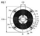
図1は、CADデータからのプリントアウト(イメージ)の第1の例示的な実施形態を示し、平面コイル12の1つの設計、および、絶縁材料層14上の貫通接続24の配置について示している。 FIG. 1 shows a first exemplary embodiment of a printout (image) from CAD data showing one design of
コイル20の磁場を強化するために、強磁性材料で作られた磁束集束器(図示せず)をコイル20の内部に挿入する。したがって、強磁性材料を受け入れるために、コイル20の内部に貫通開口部26が備えられる。 To enhance the magnetic field of
図1に示す実施形態では、外側貫通接続24aはコイル20の外側に備えられ、内側貫通接続24bはコイル20の内側に備えられている。貫通開口部26は、内側貫通接続24bがあるリング部分(リング領域)の内側に備えられている。平面コイル12のターン(巻き線部)22を配置することができる面領域は、外側の貫通接続24aが配置されるリング部分と、内側の貫通接続24bが配置される内側リング部分との間に配置される。ターン22は、コンピュータ支援製造(CAM)によって、残りの中間領域に最適に配置される。その結果、個々のターン22の間には、最小の間隔が残るのであり、ターン22を配置可能な面領域は、導電体18からなる材料でもって最適に覆われる。 In the embodiment shown in FIG. 1, the
図2は、図1と同様の図であり、図1に示す実施形態よりも好ましい平面コイル12の実施形態を示している。 FIG. 2 is a view similar to FIG. 1 and shows an embodiment of
図2に示す実施形態において、少なくとも内側貫通接続24bは、貫通開口部26と平面コイル12との間のリング部分ではなく、貫通開口部26の縁に直接備えられている。したがって、貫通接続24bは、貫通開口部26の内側に延びている。 In the embodiment shown in FIG. 2, at least the inner through-
上記に代えて、または上記ととともに、外側貫通接続24aは、平面コイル12の周りの外側リング部分の領域内ではなく、絶縁材料層14の外側に備えられることが想定される。 Alternatively or in addition, it is envisioned that the outer feed-through
このことにより、平面コイル12のターン22に使用できる表面領域は、図1の実施形態よりもかなり大きくなる。さらに、貫通開口部の直径について、図1の実施形態に比べて、平面コイル12のトータルの表面領域を増加させることなく、大幅に大きくすることができる。これにより、コイル20内に大量の強磁性材料を配置することが可能になる。 This allows the surface area available for the
方法の一実施形態において、個々の平面コイルユニット10は、それぞれが、絶縁材料層14とその上に配置された少なくとも1つまたは複数の平面コイル12を、特には図2の実施形態にしたがって備えており、CADデータに基づくコンピュータ制御下で正確に位置決めして積層される。この積層は、いずれの平面コイル12同士の間にも、単一の絶縁材料層14ののみが備えられるように行われる。この絶縁材料層14は、例えばプリプレグから形成される。 In one embodiment of the method, individual
リソグラフィープロセスを図3~6に示す。内層コア40はリソグラフィーで処理される。内層コア40は、通常、エポキシ樹脂と、ガラス布の内層42とを含んでなる。内層コア40の上面側および下面側には、導体材料層44が配置されている。 The lithographic process is illustrated in Figures 3-6. The
リソグラフィープロセスの第1のステップでは、図4に示されるように、感光性フィルム46およびフォトマスクフィルム48が、被露光体50の両面を覆うように配置される。 In the first step of the lithographic process, a
その後、被露光体50に露光が行われる。この際、感光性フィルム46は、露光された箇所にて硬化され、一方、感光性フィルム46における露光されなかった箇所は、硬化されないままである。 After that, the
露光に引き続いて、図5に示すように、フォトマスクフィルム48と、感光性フィルム46の非露光領域が除去される。 Following exposure, the
次のエッチングプロセスにおいて、露出した導体材料44は、通常、アルカリ性溶液を使用して最終的にエッチング除去されるのであり、また、残りの硬化した感光性フィルム46が除去される。図6に示すように、エポキシ樹脂及びガラス布から形成された層42と、その上配置された導体材料44のパターンとを含む構造52が残る。 In a subsequent etching process, the exposed
図7においては、図6の構造52が複数積層され、ここでは2層が、好ましくは3~15層が積層される。プリプレグ中間層54が上記の構造52の間に広げられて充填される。このように積層された構造52は、最終的にプレスで押し合わされる。このようにして、絶縁材料と導体材料の層が、複数交互に生成される。 In FIG. 7, a plurality of
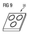
通常、図3~8にて示唆されるように、共通の内層コア40上に複数のデバイスユニット56が生成される。これにより、多量の個数までの量産が可能になる。 Typically,
大面積のリソグラフィー処理の後、内層コア40が個々のデバイスユニット56に切断される。個々のデバイスユニット56には、図9に示すように、通常、複数のコイル20が配置され、好ましくは3つまたは5つのコイル20が配置される。 After large area lithographic processing,
図10は、コイル20を通る断面の写真を示しており、コイル20は、本発明の方法の一実施形態に従って製造されている。貫通開口部26を備えたコイルの中心が左側に示され、個々の平面コイル12、及び、それらの間の絶縁材料を見てとれる。この積層された平面コイル12の束ね合わせは、例えば、キャリア基板として機能するプリント回路基板(剛性のプリント回路基板要素38)の開口部内に配置される。製造は、本明細書に記載のプロセスに従って行うことができる。その結果、図10に見られるように、平面コイルユニットの層が生成され、それらは重ね合わされて層状に配置される。導電体18から形成された個々の平面コイルユニットの間には、いずれも、絶縁材料の層が備えられ、この絶縁材料の層は、例えば、40~50μmの厚さを有する。 FIG. 10 shows a photograph of a cross section through
本発明によると、コンピュータ支援製造(CAM)によって、常に、正確に同じ具合に平面コイル12を製造し、及び/または、コンピュータ支援積層配置によって、常に、個々の平面コイル12についての相互のシンメトリー性(均整)を達成し、並びに、個々の平面コイル12の間の絶縁材料層を格段に薄くした実施形態を達成する。コンピュータ支援積層配置は、コンピュータを用いて重ね合わせて正確な位置決めすることによって、または、平面コイルユニット10を層状に重ね合わさるように製造することによって達成されうる。 According to the present invention, computer-aided manufacturing (CAM) always produces
n個積層された平面コイルユニット10における、i番目の平面コイルユニット10の導電体18についての平面コイル厚さdi,PSと、i番目の平面コイルユニット10の絶縁材料層14の層厚さdi,IMとは、次のように選択される。すなわち、好ましくは、平面コイル厚さdi,PSが、絶縁材料の層厚さdi,IM以上であるように(より大きいか、または等しいように)選択される。いずれの場合も、厚さdi,PSおよび厚さdi,IMは次のように選択される。
ここで、

このことから次のとおりとなっている。平面コイル12のターン(巻線部)22が配置されている表面領域上にて、をもたらし、コイルの束ね合わせの全体にわたって見て、導電体18の材料(例えば、銅)の割合が、絶縁体材料層14の絶縁材料と比較して大きい。このことにより、より小さな体積にて、コイル20に与えられた同じ電流で、より大きな電流密度、したがって、より強い磁場を生成できる。 From this it follows: Over the surface area where the turns 22 of the
コイル20のコンピュータ支援製造(CAM)はまた、図11aに示されるようにモノファイラー(一重巻き)方式で、並びに、図11b~11dに示されるようにマルチファイラー(多重巻き)で、個々の平面コイル20を製造する代替・選択実施形態を提供する。 Computer-aided manufacturing (CAM) of the
このようにして、互いに電気的に絶縁され、種々の方法で相互接続することができる、1つの巻線スパイラルまたは複数の巻線スパイラルを有する平面コイル12を製造することができる。 In this way,
これにより、同心円状に配置されたコイル20a、20bの製造が可能になり、これらコイルは異なる具合に接触を行うことができる。例えば、マルチファイラー(多重巻き)コイル20の異なる重ね巻き性(ファイラ性)は、差動測定に使用される。別の例示的な実施形態では、入れ子になったコイル20aの一方は、磁気発生器コイルとして使用でき、他方は、測定コイルとして使用することができる。さらに別の例示的な実施形態では、複数の入れ子になったコイルを差動測定に使用することができる。さらに別の実施形態では、相異なる、入れ子になったコイルを、ブリッジ回路の相異なる要素として使用することができる。 This allows the production of concentrically arranged
図12は、誘導性部材(inductive element)30の第1の実施例を示し、この誘導性部材30は、第1のコイル20a、第2のコイル20b、および第3のコイル20cを形成すべく、前述の方法に従って製造された平面コイルアセンブリ32を有する。 FIG. 12 shows a first embodiment of an
誘導性部材30は、アクチュエータまたはセンサーの一部として使用することができる。特に、誘導性部材30は、文献D1~D10に記載されているタイプのトルクセンサーまたは応力センサーにおけるセンサーヘッドの必須部分・部材として使用することができる。その場合、センサーヘッドは依然として強磁性増強材を含む。センサーヘッドの設計に関する詳細については、D10が引用・参照される。
センサーヘッドに使用する場合、第1のコイル20aは、例えば磁気発生器コイルとして使用して、例えば回転シャフトといった、応力の印加について測定される部材・部分にて磁場を生成するのに使用することができる。また、磁場の変化、特には応力の影響下での磁場の方向の変化を測定するにあたり、第2のコイル20bは、ための第1の測定コイルとして機能し、第3のコイル20cは第2の測定コイルとして機能する。 When used in a sensor head, the
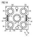
図12に見られるように、コイル20a、20b、20cは、いずれも、それぞれに重ね合わされた平面コイル12によって形成されており、磁気増強のための材料が貫通して差し込まれ得る開口部26を備えている。また、複数の貫通接続24、24bが、各貫通開口26の内壁に備えられている。誘導性部材30のさらなる実施形態が、図13および14に示されており、ここでは、第1のコイル20a、第2のコイル20b、および第3のコイル20cに加えて、第4のコイル20dおよび第5のコイル20eが備えられている。第2~第5のコイル20b~20eは、第1のコイル20aの周りに分布するようにして備えられている。第4のコイル20dは第3の測定コイルを形成することができ、第5のコイル20eは第4の測定コイルを形成することができる。 As seen in FIG. 12, the
測定コイル(例えば、第2~第5のコイル20b~20e)の相互接続は、ドイツ特許出願DE 10 2017 112 913.8に詳細に記載および示されているように行うことができる。このドイツ特許出願が、さらなる詳細に関して明示的に引用・参照される。 The interconnection of the measuring coils (eg the second to
特に、この場合の測定コイルは、発電コイルとして機能する第1のコイル20aの周りに、いわゆるX配置で配置されている。 In particular, the measuring coils in this case are arranged in a so-called X-arrangement around the
個々のコイル20、および/または、誘導性部材30に備えられる任意の他の電子構成要素の電気的接続のための接触パッド34bは、好ましくは、誘導性部材30の少なくとも1つの外縁エッジ部に配置される。 Contact pads 34b for electrical connection of the
図12に示す例示的な実施形態では、接触パッドは片側に配置されている。図13および図14に示される誘導性部材30の例示的な実施形態では、接触パッド34は、誘導性部材30の互いに向き合う両側にて、長方形の切り取り部(凹部)36の内部に備えられる。詳細Aによって示されるように、接触パッドの1つは、試験パッドとして形成することができる。 In the exemplary embodiment shown in FIG. 12, the contact pads are arranged on one side. In the exemplary embodiment of
図12および13にしたがうセンサーヘッドに使用される誘導性部材30を製造するための方法についての好ましい実施形態は、文献D11(特許文献10)で説明されている基本原理から知られるように、個々のコイル20、20a~20eのための空洞が、剛性のプリント回路基板要素38に形成されていることが想定されている。 A preferred embodiment for the method for manufacturing the
コイル20a~20eの個々の層を形成する個々の平面コイル12は、上述のように、可撓性プリント回路基板16上に平面コイルユニット10としてまとめて製造されるのであり、それぞれに複数の平面コイルを有するn個の平面コイルユニット10が、コンピュータ制御下で積層されて配置されるか、またはコンピュータ制御下で積層されて製造される。したがって、個々の平面コイル12から形成されたコイル20、20a~20eが積層された平面コイルアセンブリ32が形成される。 The individual
本発明の一実施形態では、個々のコイルは、カッティングパンチによってまとめて切り出され、剛性プリント回路基板部材38の個々の空洞に移送される。 In one embodiment of the present invention, individual coils are cut together by a cutting punch and transferred to individual cavities in rigid printed
本発明の別の実施形態では、平面コイルユニット10を層状に重ね合わして形成される平面コイルアセンブリ32が、誘導性部材30として使用され、その結果、剛性のプリント回路基板部材38は必要とされない。 In another embodiment of the present invention, a
図1および2に示されるように、コイル20は、例えば、平面コイル12あたりにトータルで4~100個のターンから(4~100の巻き数で)、例えば15個のターンから製造することができる。ここで、n = 8の層が重ねられて用いられる。好ましくは、nは3~15の範囲にある。 As shown in FIGS. 1 and 2, the
図1に示すように、ターン(巻線)の表面領域の内側と外側にあるリング部分で貫通接続を使用する場合、輪郭の箇所の銅の量は、たとえば、典型的には0.3mmに設定できる。 As shown in Figure 1, when feedthroughs are used in the inner and outer ring portions of the surface area of the turns (windings), the amount of copper at the contour points is typically set to 0.3 mm, for example. can.
図2に示すように、貫通接続が輪郭の箇所に備えられる場合、ターン(巻線)22による表面の使用割合は、大幅に改善される。 As shown in FIG. 2, the surface area utilization by
10 平面コイルユニット
12 平面コイル
14 絶縁材料層
16 フレキシブルプリント回路基板
18 導電体
20 コイル
20a 第1のコイル
20b 第2のコイル
20c 第3のコイル
20d 第4のコイル
20e 第5のコイル
22 ターン(巻線部)
24 貫通接続
24a 外部貫通接続
24b 内部貫通接続
26 貫通開口
30 誘導性部材
32 平面コイルアセンブリ
34 コンタクトパッド
36 休憩
38 リジッド(剛性)プリント回路基板部材
40 内層コア
42 エポキシ樹脂とガラス布の層
44 導体材料
46 感光フィルム
48 フォトマスクフィルム
50 被露光体
52 (図6の)構造
54 プリプレグ中間層
56 デバイスユニット
10
24 through-
Claims (5)
Translated fromJapanesea)コンピュータ支援製造により、電気絶縁材料から作られた厚みdi,IMの絶縁材料層(14)の上に、導電体から作られて平面コイル厚さdi,PSを有する少なくとも1つの平面コイル(12)を製造することによって、i番目の平面コイルユニット(10)を作成する。ここで、iは1からnに等しい。
b)平面コイル(12)同士の間に絶縁材料層(14)を挟み込むようにして、平面コイルユニット(10)を積層して配置する。
ここで、厚みdi,PSおよびdi,IMは、下式を満たすように選択される。

a7)互いに分離された複数のコイルトラックを有する少なくとも1つの平面コイル(12)の製造。
a10)マルチファイラー(多重巻き)コイル(20)における、入れ子になったコイル(20a)の一方は、磁気発生器コイルとして使用し、他方は、測定コイルとして使用する。
d)平面コイルユニット(10)における重ね合わされた平面コイル(12)の中心を通る少なくとも1つの貫通開口部(26)を形成する。
6.1 少なくとも1つの貫通開口部(26)にて、少なくとも1つの貫通接続(24)を使用して、重ね合わされた平面コイル(12)を電気的に接続する。
6.2 磁束集束器を少なくとも1つの貫通開口部(26)に挿入する。
6.3 ステップa)の前、および/または、ステップb)の前またはステップb)の後に、絶縁材料層(14)が貫通開口部(26)の各領域に備えられるように、ステップd)を実行する。Amanufacturing method for manufacturing a planar coil assembly (32) in which n planar coil units (10) are superimposed, wherein n is a natural number greater than 1, and comprising the followingsteps a) and b):A manufacturing method wherein a) includes steps a6)-a7) and a10) below, and is characterized by d) below and all of 6.1-6.3 below .
a) at least one plane made of an electrical conductor and having a planar coil thickness di,PS on top of an insulating material layer (14) of thickness di,IM made of an electrically insulating material by computer-aided manufacturing; The i-th planar coil unit (10) is created by manufacturing the coil (12). where i is equal to 1 to n.
b) The planar coil units (10) are stacked such that the insulating material layer (14) is sandwiched between the planar coils (12).
where the thicknesses di,PS and di,IM are selected to satisfy the following equations.
a7) Manufacturing at least one planar coil (12) with a plurality of coil tracks separated from each other.
a10) In a multifilar coil (20), one of the nested coils (20a) is used as a magnetic generator coil and the other as a measuring coil.
d) forming at least one through opening (26) through the center of the superimposed planar coils (12) in the planar coil unit (10);
6.1 Electrically connecting the superimposed planar coils (12) using at least one through-connection (24) in at least one through-opening (26).
6.2 Insert the flux concentrator into at least one through opening (26).
6.3 Before step a) and/or before step b) or after step b) step d) such that a layer of insulating material (14) is provided in each region of the through-openings (26) to run.
a)コンピュータ支援製造により、電気絶縁材料から作られた厚みdi,IMの絶縁材料層(14)の上に、導電体から作られて平面コイル厚さdi,PSを有する少なくとも1つの平面コイル(12)を製造することによって、i番目の平面コイルユニット(10)を作成する。ここで、iは1からnに等しい。
b)平面コイル(12)同士の間に絶縁材料層(14)を挟み込むようにして、平面コイルユニット(10)を積層して配置する。
ここで、厚みdi,PSおよびdi,IMは、下式を満たすように選択される。

a7)互いに分離された複数のコイルトラックを有する少なくとも1つの平面コイル(12)の製造。
a9)互いに軸対称または点対称に配置された、平面コイルユニットごとの、少なくとも第1、第2、第3および第4の測定平面コイルと、中央の磁気発生器平面コイルとの製造。
d)平面コイルユニット(10)における重ね合わされた平面コイル(12)の中心を通る少なくとも1つの貫通開口部(26)を形成する。
6.1 少なくとも1つの貫通開口部(26)にて、少なくとも1つの貫通接続(24)を使用して、重ね合わされた平面コイル(12)を電気的に接続する。
6.2 磁束集束器を少なくとも1つの貫通開口部(26)に挿入する。
6.3 ステップa)の前、および/または、ステップb)の前またはステップb)の後に、絶縁材料層(14)が貫通開口部(26)の各領域に備えられるように、ステップd)を実行する。A manufacturing method for manufacturing a planar coil assembly (32) in which n planar coil units (10) are superimposed, wherein n is a natural number greater than 1, comprising the following a) and b), and step a ) includes steps a6)-a7) and a9) below and is characterized by all of d) below and 6.1-6.3 below.
a)at least oneplane made of an electrical conductor and having a planar coil thickness di,PS on top of an insulating material layer (14) of thickness di,IMmade of an electrically insulating material by computer-aided manufacturing;The i-th planar coil unit (10) is created by manufacturing the coil (12). where i is equal to 1 to n.
b) The planar coil units (10) are stacked such that the insulating material layer (14) is sandwiched between the planar coils (12).
where the thicknesses di,PSand di,IMare selected to satisfy the following equations.
a7) Manufacturing at least one planar coil (12) with a plurality of coil tracks separated from each other.
a9) Manufacture of at least a first, second, third and fourth measuring planar coil and a central magnetic generator planar coil per planar coil unit arranged axisymmetrically or point-symmetrically to each other.
d) forming at least one through opening (26) through the center of the superimposed planar coils (12) in the planar coil unit (10);
6.1 Electrically connecting the superimposed planar coils (12) using at least one through-connection (24) in at least one through-opening (26).
6.2 Insert the flux concentrator into at least one through opening (26).
6.3 Before step a) and/or before step b) or after step b) step d) such that a layer of insulating material (14) is provided in each region of the through-openings (26) to run.
c)平面コイルユニット(10)における重ね合わされた複数の平面コイル(12)を電気的に接続することで、少なくとも1つの磁気コイルを形成する。3. Themanufacturing method according to claim 1or 2 , characterized by the following c).
c) formingat least one magnetic coil by electrically connecting a plurality of superimposed planar coils (12) in the planar coil unit (10);
Applications Claiming Priority (5)
| Application Number | Priority Date | Filing Date | Title |
|---|---|---|---|
| DE102018108869 | 2018-04-13 | ||
| DE102018108869.8 | 2018-04-13 | ||
| DE102018114785.6ADE102018114785A1 (en) | 2018-04-13 | 2018-06-20 | Method for producing a planar coil arrangement and a sensor head provided therewith |
| DE102018114785.6 | 2018-06-20 | ||
| PCT/EP2019/059162WO2019197500A1 (en) | 2018-04-13 | 2019-04-10 | Method for producing a planar coil assembly and a sensor head provided with same |
Publications (2)
| Publication Number | Publication Date |
|---|---|
| JP2021521645A JP2021521645A (en) | 2021-08-26 |
| JP7145229B2true JP7145229B2 (en) | 2022-09-30 |
Family
ID=68053122
Family Applications (1)
| Application Number | Title | Priority Date | Filing Date |
|---|---|---|---|
| JP2020555805AActiveJP7145229B2 (en) | 2018-04-13 | 2019-04-10 | Manufacturing method of planar coil assembly and sensor head provided with the same |
Country Status (6)
| Country | Link |
|---|---|
| US (1) | US11948735B2 (en) |
| EP (1) | EP3776605B1 (en) |
| JP (1) | JP7145229B2 (en) |
| CN (1) | CN112204681B (en) |
| DE (1) | DE102018114785A1 (en) |
| WO (1) | WO2019197500A1 (en) |
Families Citing this family (7)
| Publication number | Priority date | Publication date | Assignee | Title |
|---|---|---|---|---|
| DE102019102454B3 (en) | 2019-01-31 | 2020-08-06 | Trafag Ag | Arrangement and method for measuring a mechanical load on a test object while detecting changes in the magnetic field |
| DE102021123394A1 (en) | 2021-09-09 | 2023-03-09 | Trafag Ag | Load measuring arrangement for magnetostrictive measuring of a load on a test object and manufacturing method |
| DE102021123392A1 (en) | 2021-09-09 | 2023-03-09 | Trafag Ag | Load measuring arrangement and load measuring method for measuring a load on a test object with an auxiliary transmission element |
| DE102022129926B4 (en) | 2022-11-11 | 2025-05-08 | Trafag Ag | Sensor head for load measuring device with magnetic coils |
| WO2024236101A1 (en)* | 2023-05-17 | 2024-11-21 | Nv Bekaert Sa | Coil for eddy current sensor |
| DE102023113348A1 (en) | 2023-05-22 | 2024-11-28 | Trafag Ag | Sensor for frontal magnetostrictive measurement of loads, load measuring device and measuring arrangement provided therewith, load measuring method and manufacturing method |
| DE102023122075B4 (en) | 2023-08-17 | 2025-08-28 | Trafag Ag | Distance-variable measuring device |
Citations (9)
| Publication number | Priority date | Publication date | Assignee | Title |
|---|---|---|---|---|
| JP2004212375A (en) | 2002-12-31 | 2004-07-29 | Samsung Electro Mech Co Ltd | Sensor for sensing feeble magnetic field, and method for manufacturing the same, using printed circuit board technology |
| JP2008141203A (en) | 2006-11-29 | 2008-06-19 | Ud Tech Kk | Transformer device |
| JP2010192889A (en) | 2009-01-22 | 2010-09-02 | Ngk Insulators Ltd | Layered inductor |
| JP2011082371A (en) | 2009-10-08 | 2011-04-21 | Sony Corp | Laminated inductor-incorporating multilayer wiring board, tuner module, and electronic apparatus |
| JP2013058755A (en) | 2011-09-07 | 2013-03-28 | Commissariat A L'energie Atomique Et Aux Energies Alternatives | Printed circuit board comprising two coils |
| JP2013138146A (en) | 2011-12-28 | 2013-07-11 | Taiyo Yuden Co Ltd | Laminated coil and electronic component using the same |
| US20150302967A1 (en) | 2012-12-15 | 2015-10-22 | Arthur L. Jenkins | Multilayered electromagnetic assembly |
| JP2017199766A (en) | 2016-04-26 | 2017-11-02 | 株式会社村田製作所 | Multilayer coil array and module |
| DE102016122172A1 (en) | 2016-07-25 | 2018-01-25 | Trafag Ag | Sensor head for a force or torque sensor |
Family Cites Families (28)
| Publication number | Priority date | Publication date | Assignee | Title |
|---|---|---|---|---|
| DE110599C (en) | ||||
| US3011340A (en) | 1957-06-26 | 1961-12-05 | Asea Ab | Means for measuring a torsional stress in a shaft of magnetostrictive material |
| US3311818A (en) | 1963-03-11 | 1967-03-28 | Api Instr Company | Non-contact apparatus for magnetically measuring strain |
| US4135391A (en) | 1977-11-22 | 1979-01-23 | Asea Aktiebolag | Torque transducer |
| DE3031997C2 (en) | 1980-08-25 | 1986-01-16 | Licentia Patent-Verwaltungs-Gmbh, 6000 Frankfurt | Arrangement for non-contact measurement of static and dynamic torques |
| DE8511143U1 (en) | 1985-04-16 | 1985-06-27 | Dietrich Grünau GmbH & Co KG, 7778 Markdorf | Measuring hub for torque and speed measurement on rotating machine parts |
| JPH02221830A (en) | 1989-02-22 | 1990-09-04 | Kubota Ltd | Magnetostrictive torque sensor |
| DE4105999A1 (en)* | 1990-12-20 | 1992-06-25 | Nippon Filcon Kk | Foil coil for superconductive devices e.g. linear motor - has etched conductor coils on plates applied to opposite surfaces of stacked, insulating substrate plates |
| JP4010920B2 (en)* | 2002-09-30 | 2007-11-21 | Tdk株式会社 | Inductive element manufacturing method |
| US8466764B2 (en)* | 2006-09-12 | 2013-06-18 | Cooper Technologies Company | Low profile layered coil and cores for magnetic components |
| EP2107577B1 (en) | 2008-03-31 | 2016-10-19 | Würth Elektronik Rot am See GmbH & Co. KG | Inductive component and method for its production |
| EP2370981B1 (en) | 2008-12-03 | 2012-10-10 | Planarmag, Inc. | An integrated planar variable transformer with embedded magnetic core |
| DE102009008074A1 (en) | 2009-02-10 | 2010-08-12 | Siemens Aktiengesellschaft | Measuring arrangement and use for detecting the torque |
| US9300046B2 (en)* | 2009-03-09 | 2016-03-29 | Nucurrent, Inc. | Method for manufacture of multi-layer-multi-turn high efficiency inductors |
| DE102010016779A1 (en) | 2010-05-04 | 2011-11-10 | Cicor Management AG | Method for producing a flexible circuit arrangement |
| US20110298811A1 (en) | 2010-06-02 | 2011-12-08 | Apple Inc. | Flexible printed circuit to glass assembly system and method |
| WO2012053439A1 (en)* | 2010-10-21 | 2012-04-26 | Tdk株式会社 | Coil component and method for producing same |
| DE102011075400A1 (en) | 2011-05-06 | 2012-11-08 | Siemens Ag | Torque sensor assembly and shaft with a torque sensor assembly |
| KR20130077400A (en)* | 2011-12-29 | 2013-07-09 | 삼성전기주식회사 | Thin film type coil component and fabricating method thereof |
| KR101771731B1 (en)* | 2012-08-28 | 2017-08-25 | 삼성전기주식회사 | Multi-layered chip electronic component |
| US20150116950A1 (en)* | 2013-10-29 | 2015-04-30 | Samsung Electro-Mechanics Co., Ltd. | Coil component, manufacturing method thereof, coil component-embedded substrate, and voltage adjustment module having the same |
| DE102013115009B4 (en)* | 2013-12-31 | 2020-02-06 | Trafag Ag | Density monitor with separate housing parts and assembly process |
| EP2957880B8 (en)* | 2014-06-16 | 2018-08-22 | Franz Braunschmid | Layout of elementary spring bodies for force or torque sensors |
| KR101751117B1 (en)* | 2015-07-31 | 2017-06-26 | 삼성전기주식회사 | Coil electronic part and manufacturing method thereof |
| US10777342B2 (en)* | 2016-06-15 | 2020-09-15 | Taiyo Yuden Co., Ltd. | Coil component and method for manufacturing the same |
| JP2018018868A (en)* | 2016-07-26 | 2018-02-01 | イビデン株式会社 | Coil substrate and manufacturing method thereof |
| US20180038461A1 (en)* | 2016-08-05 | 2018-02-08 | Ecole Polytechnique Federale De Lausanne (Epfl) | Planar Pop-Up Actuator Device with Embedded Electro-Magnetic Actuation |
| DE102017112913B4 (en) | 2017-06-12 | 2025-01-30 | Trafag Ag | load measurement method, load measurement device and load measurement arrangement |
- 2018
- 2018-06-20DEDE102018114785.6Apatent/DE102018114785A1/enactivePending
- 2019
- 2019-04-10EPEP19718622.4Apatent/EP3776605B1/enactiveActive
- 2019-04-10JPJP2020555805Apatent/JP7145229B2/enactiveActive
- 2019-04-10CNCN201980032244.9Apatent/CN112204681B/enactiveActive
- 2019-04-10WOPCT/EP2019/059162patent/WO2019197500A1/ennot_activeCeased
- 2019-04-10USUS17/046,911patent/US11948735B2/enactiveActive
Patent Citations (9)
| Publication number | Priority date | Publication date | Assignee | Title |
|---|---|---|---|---|
| JP2004212375A (en) | 2002-12-31 | 2004-07-29 | Samsung Electro Mech Co Ltd | Sensor for sensing feeble magnetic field, and method for manufacturing the same, using printed circuit board technology |
| JP2008141203A (en) | 2006-11-29 | 2008-06-19 | Ud Tech Kk | Transformer device |
| JP2010192889A (en) | 2009-01-22 | 2010-09-02 | Ngk Insulators Ltd | Layered inductor |
| JP2011082371A (en) | 2009-10-08 | 2011-04-21 | Sony Corp | Laminated inductor-incorporating multilayer wiring board, tuner module, and electronic apparatus |
| JP2013058755A (en) | 2011-09-07 | 2013-03-28 | Commissariat A L'energie Atomique Et Aux Energies Alternatives | Printed circuit board comprising two coils |
| JP2013138146A (en) | 2011-12-28 | 2013-07-11 | Taiyo Yuden Co Ltd | Laminated coil and electronic component using the same |
| US20150302967A1 (en) | 2012-12-15 | 2015-10-22 | Arthur L. Jenkins | Multilayered electromagnetic assembly |
| JP2017199766A (en) | 2016-04-26 | 2017-11-02 | 株式会社村田製作所 | Multilayer coil array and module |
| DE102016122172A1 (en) | 2016-07-25 | 2018-01-25 | Trafag Ag | Sensor head for a force or torque sensor |
Also Published As
| Publication number | Publication date |
|---|---|
| DE102018114785A1 (en) | 2019-10-17 |
| JP2021521645A (en) | 2021-08-26 |
| EP3776605C0 (en) | 2023-08-02 |
| EP3776605B1 (en) | 2023-08-02 |
| CN112204681A (en) | 2021-01-08 |
| WO2019197500A1 (en) | 2019-10-17 |
| US11948735B2 (en) | 2024-04-02 |
| CN112204681B (en) | 2023-05-30 |
| US20210383969A1 (en) | 2021-12-09 |
| EP3776605A1 (en) | 2021-02-17 |
Similar Documents
| Publication | Publication Date | Title |
|---|---|---|
| JP7145229B2 (en) | Manufacturing method of planar coil assembly and sensor head provided with the same | |
| CN104078192B (en) | Electronic component and manufacturing method thereof | |
| JP2022116126A (en) | Laminated electronic component and manufacturing method thereof | |
| US6683522B2 (en) | Planar miniature inductors and transformers | |
| TW554354B (en) | Multilayer inductor | |
| JP2008112982A (en) | High precision rogowski current transformer of improved type | |
| JP2016515305A (en) | Apparatus and method for planar magnetic technology using laminated polymer | |
| WO2005031764A1 (en) | Laminated magnetic component and process for producing the same | |
| CN109036831A (en) | Coil component and its manufacturing method | |
| JP2005217268A (en) | Electronic component | |
| WO2002095775A1 (en) | Planar miniature inductors and transformers and miniature transformers for millimachined instruments | |
| JP2001196240A (en) | Multilayer inductor | |
| JP2008109139A (en) | Coil having several coil branches and microinductor having one of the coils | |
| CN112051431A (en) | Current sensor and measuring system comprising such a current sensor | |
| JP2009027102A (en) | Vibration sensor using laminated coil and laminated coil | |
| JP2005044952A (en) | Common mode choke coil and manufacturing method thereof, and common mode choke coil array | |
| WO2023145106A1 (en) | Coil component and circuit board provided with same | |
| JPH05284697A (en) | Coil body and manufacturing method thereof | |
| JP7347037B2 (en) | Manufacturing method of electronic components | |
| JP2004311828A (en) | Stacked common mode choke coil and its manufacturing method | |
| JP2017152500A (en) | Coil parts | |
| JP2002513511A (en) | Via-free integrated inductive devices for electromagnetic applications | |
| JP7623125B2 (en) | Coil parts | |
| JP2008130940A (en) | Method for manufacturing winding type electronic component | |
| JP2025012913A (en) | Magnetic sensor element and its manufacturing method |
Legal Events
| Date | Code | Title | Description |
|---|---|---|---|
| A621 | Written request for application examination | Free format text:JAPANESE INTERMEDIATE CODE: A621 Effective date:20201210 | |
| A131 | Notification of reasons for refusal | Free format text:JAPANESE INTERMEDIATE CODE: A131 Effective date:20220125 | |
| A521 | Request for written amendment filed | Free format text:JAPANESE INTERMEDIATE CODE: A523 Effective date:20220408 | |
| TRDD | Decision of grant or rejection written | ||
| A01 | Written decision to grant a patent or to grant a registration (utility model) | Free format text:JAPANESE INTERMEDIATE CODE: A01 Effective date:20220830 | |
| A61 | First payment of annual fees (during grant procedure) | Free format text:JAPANESE INTERMEDIATE CODE: A61 Effective date:20220916 | |
| R150 | Certificate of patent or registration of utility model | Ref document number:7145229 Country of ref document:JP Free format text:JAPANESE INTERMEDIATE CODE: R150 | |
| R250 | Receipt of annual fees | Free format text:JAPANESE INTERMEDIATE CODE: R250 |