JP7139653B2 - optical device - Google Patents
optical deviceDownload PDFInfo
- Publication number
- JP7139653B2 JP7139653B2JP2018066986AJP2018066986AJP7139653B2JP 7139653 B2JP7139653 B2JP 7139653B2JP 2018066986 AJP2018066986 AJP 2018066986AJP 2018066986 AJP2018066986 AJP 2018066986AJP 7139653 B2JP7139653 B2JP 7139653B2
- Authority
- JP
- Japan
- Prior art keywords
- optical
- housing
- optical modulator
- functional element
- recess
- Prior art date
- Legal status (The legal status is an assumption and is not a legal conclusion. Google has not performed a legal analysis and makes no representation as to the accuracy of the status listed.)
- Active
Links
- 230000003287optical effectEffects0.000titleclaimsdescription282
- 230000001902propagating effectEffects0.000claimsdescription5
- 239000013307optical fiberSubstances0.000description31
- ORQBXQOJMQIAOY-UHFFFAOYSA-NnobeliumChemical compound[No]ORQBXQOJMQIAOY-UHFFFAOYSA-N0.000description26
- 238000009826distributionMethods0.000description21
- 230000007613environmental effectEffects0.000description13
- 230000004048modificationEffects0.000description11
- 238000012986modificationMethods0.000description11
- 230000005540biological transmissionEffects0.000description8
- 230000010287polarizationEffects0.000description7
- 239000000470constituentSubstances0.000description4
- 239000000758substrateSubstances0.000description4
- 239000004020conductorSubstances0.000description2
- 238000004519manufacturing processMethods0.000description2
- 238000003466weldingMethods0.000description2
- 238000006243chemical reactionMethods0.000description1
- 238000004891communicationMethods0.000description1
- 239000012141concentrateSubstances0.000description1
- 230000008602contractionEffects0.000description1
- 230000008878couplingEffects0.000description1
- 238000010168coupling processMethods0.000description1
- 238000005859coupling reactionMethods0.000description1
- 238000002788crimpingMethods0.000description1
- 238000010586diagramMethods0.000description1
- 239000000835fiberSubstances0.000description1
- 230000007774longtermEffects0.000description1
- 239000000463materialSubstances0.000description1
- 238000005259measurementMethods0.000description1
- 238000003825pressingMethods0.000description1
- 239000010453quartzSubstances0.000description1
- VYPSYNLAJGMNEJ-UHFFFAOYSA-Nsilicon dioxideInorganic materialsO=[Si]=OVYPSYNLAJGMNEJ-UHFFFAOYSA-N0.000description1
- 229910000679solderInorganic materials0.000description1
Images


Landscapes
- Optical Couplings Of Light Guides (AREA)
- Optical Modulation, Optical Deflection, Nonlinear Optics, Optical Demodulation, Optical Logic Elements (AREA)
Description
Translated fromJapanese本発明は、光デバイスに関する。 The present invention relates to optical devices.
光通信システムを構成する光伝送装置や、光計測装置には、特定の機能を備える種々の光デバイスが用いられる。このような光デバイスは、一般に、所定の機能を有する光機能素子(例えば、光変調を行う光変調素子)と、光機能素子を収容する筐体と、筐体外部から光機能素子に光を入射する入力用ファイバと、光機能素子から出射する光を筐体外部へ導く出力用光ファイバと、を備える。また、光デバイスは、上記光機能素子が電気信号に基づいて動作する場合には、光機能素子との間で電気信号を入出力するための電気端子を備える(例えば、特許文献1参照)。 2. Description of the Related Art Various optical devices having specific functions are used for optical transmission devices and optical measurement devices that constitute optical communication systems. Such an optical device generally includes an optical functional element having a predetermined function (for example, an optical modulation element that modulates light), a housing that accommodates the optical functional element, and light from outside the housing to the optical functional element. It has an input fiber for incidence and an output optical fiber for guiding light emitted from the optical functional element to the outside of the housing. Further, the optical device includes an electrical terminal for inputting/outputting an electrical signal to/from the optical functional element when the optical functional element operates based on an electrical signal (see, for example, Patent Document 1).
そして、光デバイスでは、一般に、入射光ファイバ、出射光ファイバ、及び電気端子は、それぞれ、光デバイスを構成する筐体に固定され、筐体の壁に設けられた孔を介して、光機能素子との間での光の入出射や電気信号の入出力を行う。 In an optical device, an input optical fiber, an output optical fiber, and an electrical terminal are generally fixed to a housing that constitutes the optical device, and are connected to the optical functional element through holes provided in the wall of the housing. Input and output of light and input and output of electrical signals are performed between and.
また、場合によっては、例えば光デバイスが実装される回路基板との接続を容易にすべく、上記筐体のうち回路基板とのインタフェースが行われる部分に特殊な形状の加工(例えば凹部の形成)が施されることもある。 In some cases, for example, in order to facilitate connection with a circuit board on which an optical device is mounted, the portion of the housing that interfaces with the circuit board is processed into a special shape (for example, forming a recess). is sometimes applied.
このような、筐体における光の入出射や電気信号の入出力のための孔や、上記インタフェースのための加工部分は、加工歪や機械応力を発生し易く、機械強度も当該筐体の他の部分に比べて低下しやすい。 Such holes for the input and output of light and the input and output of electrical signals in the housing, and the processed parts for the interface, are likely to generate processing strain and mechanical stress, and the mechanical strength is not the same as that of the housing. It is easy to fall compared with the part of .
このため、例えば、筐体を気密封止する際に筐体に加わる圧着圧力(例えば筐体の一部であるケースに、筐体の他の一部であるカバーをシーム溶接する際の押圧力)やシーム溶接時に発生する溶接部分の応力により、上記機械強度が低下した部分に歪が集中し、筐体に形状変化又は変形が発生し得る。このような筐体の変形は、筐体内部における光学系の配置を変化させ、無視し得ない光学特性の変化を生じさせ得る。その結果、光デバイスの製造歩留まりを低下させる要因となり得る。 For this reason, for example, the crimping pressure applied to the housing when the housing is airtightly sealed (for example, the pressing force when seam-welding the cover, which is another part of the housing, to the case, which is a part of the housing) ) and the stress of the welded portion generated during seam welding, strain concentrates on the portion where the mechanical strength is lowered, and the housing may be deformed or deformed. Such deformation of the housing may change the arrangement of the optical system inside the housing, causing a non-negligible change in optical characteristics. As a result, it can be a factor in lowering the manufacturing yield of optical devices.
また、環境温度が変動した場合、上記の如く機械応力が発生し易く機械強度が低下した上記孔や加工部分には、筐体素材の熱膨張収縮による応力集中も発生しやすく、上記と同様に筐体内部の光学系配置に変化が生じ得る。その結果、温度変動の際においても、上記と同様に、光学特性に無視し得ない変動が生じ得る。 In addition, when the environmental temperature fluctuates, stress concentration due to thermal expansion and contraction of the housing material is likely to occur in the above-mentioned holes and processed parts where mechanical stress is likely to occur and mechanical strength is reduced as described above. Changes may occur in the optical system arrangement inside the housing. As a result, in the same way as described above, non-negligible fluctuations may occur in the optical characteristics even when the temperature fluctuates.
特に、光デバイスを光伝送装置等の装置筐体の角部付近に実装し得るように、光ファイバや電気端子を光デバイス筐体の一の面に集中配置した場合には、光デバイス筐体における歪や応力の集中又は偏在が発生しやすく、当該光デバイスにおける上記のような光学特性の変動は、製造歩留まりの観点だけでなく長期信頼性の面からも、大きな課題となり得る。 In particular, when optical fibers and electrical terminals are centrally arranged on one surface of an optical device housing so that the optical device can be mounted near the corners of the housing of an optical transmission device or the like, the optical device housing Concentration or maldistribution of strain and stress in the optical device tends to occur, and the fluctuation in optical characteristics of the optical device as described above can pose a major problem not only from the viewpoint of manufacturing yield but also from the viewpoint of long-term reliability.
上記背景より、光デバイスにおいて、筐体における歪の偏在や環境温度変動時の応力の偏在を抑制して、より安定な光学特性を実現することが望まれている。 From the above background, in optical devices, it is desired to realize more stable optical characteristics by suppressing the uneven distribution of strain in the housing and the uneven distribution of stress due to environmental temperature fluctuations.
本発明の一の態様は、所定の機能を有する光機能素子と、前記光機能素子を収容する筐体と、を備え、前記光機能素子は、光導波路と当該光導波路を伝搬する光波を制御する電極が設けられた光導波路素子であって、前記筐体の少なくとも一の側面には、当該筐体の外部と前記光機能素子との間で光及び又は電気信号の入出力を行うための孔及び又は凹部が設けられており、前記筐体の前記孔及び又は凹部が設けられたそれぞれの側面に対向する他の側面のそれぞれには、対応する前記孔及び又は凹部に対向する位置に、歪抑制手段である凹部が設けられている。
本発明の他の態様によると、前記歪抑制手段である凹部は、前記他の側面のうち前記筐体の内面に設けられている。
本発明の他の態様によると、前記筐体の前記孔及び又は凹部が設けられたそれぞれの側面の厚さに対し、当該側面に対向する他の側面のそれぞれの厚さが薄く構成されている。
本発明の他の態様によると、前記筐体の外部と前記光機能素子との間で光の入力を行うための孔及び光の出力を行うための孔が、前記筐体の同じ側面に設けられている。
本発明の他の態様によると、前記筐体の外部と前記光機能素子との間で光の入力を行うための孔及び光の出力を行うための孔が、前記筐体の互いに隣接する2つの側面にそれぞれ設けられている。
本発明の他の態様によると、前記筐体の外部と前記光機能素子との間で電気信号の入出力を行う電気端子を設けるための孔及び又は凹部が、前記筐体の前記同じ側面に設けられている。
本発明の他の態様は、所定の機能を有する光機能素子と、前記光機能素子を収容する筐体と、を備え、前記光機能素子は、光導波路と当該光導波路を伝搬する光波を制御する電極が設けられた光導波路素子であって、前記筐体の一の面には、当該筐体の外部と前記光機能素子との間で電気信号の入出力を行うための凹部が設けられており、前記筐体の前記凹部が設けられた面には、当該凹部に対し、当該面の形状の中心線を挟んで対称な位置に、歪抑制手段である凹部が設けられている、光デバイスである。One aspect of the present invention comprises an optical functional element having a predetermined function, and a housing for housing the optical functional element,wherein the optical functional element controls an optical waveguide and a light wave propagating through the optical waveguide. an optical waveguide element provided with an electrode for inputting and outputting light and/or electric signals between the outside of the housing and the optical functional element on at least one side surface of the housing. Holes and/or recesses are provided, and on each of the other side surfaces of the housing that face the respective side surfaces provided with the holesand /or recesses, at positions facing the corresponding holes and/or recesses, A concave portion is provided as a strain suppressing means.
According to another aspect of the present invention, the recess, which is the distortion suppressing means, is provided on the inner surface of the housing among the other side surfaces.
According to another aspect of the present invention, the thickness of each of the side surfaces of the housing on which the holes and/or recesses are provided is thinner than the thickness of each of the other side surfaces facing the side surface. .
According to another aspect of the present invention,a hole for inputting light and a hole for outputting light between the outside of the housing and the optical functional element are provided on the same side surface of the housing. It is
According to another aspect of the present invention, a hole for inputting light and a hole for outputting light between the outside of the housing and the optical functional element are formed in the housing adjacent to each other. provided on each side.
According to another aspect of the present invention, holes and/or recesses for providing electrical terminals for inputting and outputting electrical signals between the outside of the housing and the optical functional element are formed on the same side surface of the housing. is provided.
Another aspect of the present invention comprises an optical functional element having a predetermined function, and a housing for housing the optical functional element,wherein the optical functional element controls an optical waveguide and a light wave propagating through the optical waveguide. An optical waveguide element provided with an electrode that connects the optical functional element, wherein one surface of the housing is provided with a concave portion for inputting and outputting electrical signals between the outside of the housing and the optical functional element. and the surface of the housing provided with the recess is provided with a recess, which is a distortion suppressing means, at a symmetrical position with respect to the recess with respect to the center line of the shape of the surface. Device.
本発明によれば、筐体における加工歪の集中や環境温度変動時の応力集中を防止して、より安定な光学特性を有する光デバイスを実現することできる。 According to the present invention, it is possible to realize an optical device having more stable optical characteristics by preventing the concentration of processing strain in the housing and the concentration of stress when the environmental temperature fluctuates.
以下、図面を参照して、本発明の実施形態について説明する。
〔第1実施形態〕
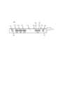
図1は、本発明の第1の実施形態に係る光デバイスである光変調器100の構成を示す平面図、図2は、光変調器100の側面図である。この光変調器100は、例えば光伝送システムを構成する光送信装置に用いられる。なお、光変調器100は、本発明に係る光デバイスの一例であって、以下に示す光変調器100の構成は、筐体内に光機能素子を備えて当該筐体に光の入出射を行う光ファイバや電気端子が設けられる光デバイスにおいて広く一般に用いることができる。Hereinafter, embodiments of the present invention will be described with reference to the drawings.
[First embodiment]
FIG. 1 is a plan view showing the configuration of an
光変調器100は、所定の機能として光変調機能を有する光機能素子である光変調素子102と、光変調素子102を収容する筐体104と、を備える。ここで、筐体104は、例えば、平面視が略長方形であり、図1の図示左右方向に延びる長辺側側面と、図示上下方向に延びる短辺側側面を有する。また、光変調器100は、筐体104の外部から光変調素子102に光を入射するための入力用光ファイバである光ファイバ108と、光変調素子102から出力される光を筐体104の外部へ導く出力用光ファイバである光ファイバ110と、を備える。 The
筐体104は、光変調素子102が固定されるケース114aと、カバー114bと、で構成されている。なお、筐体104内部における構成の理解を容易するため、図1においては、カバー114bの一部のみを図示中央に示しているが、実際には、カバー114bは、箱状のケース114aの全体を覆うように配されて筐体104の内部を気密封止する。 The
光変調素子102は、例えばLN基板上に設けられた4つのマッハツェンダ型光導波路と、当該マッハツェンダ型光導波路上にそれぞれ設けられて光導波路内を伝搬する光波を変調する4つのRF電極(高周波電極)と、を備えた、光導波路素子であるDP―QPSK光変調器である。 The
光ファイバ108は、筐体104(のケース114a)の一の長辺側側面である側面112(図1における図示下の面であって、図2に示す面)に固定されており、当該側面112に設けられた孔(貫通穴)116を通って、例えば、石英等で構成されるPLC(プレーナ光波回路、Planar Lightwave Circuit)118の光導波路(不図示)に対し光学的に結合されている。これにより、光ファイバ108から入射する光は、PLC118を介して光変調素子102に入射される。なお、以下において貫通穴を単に孔と称する。前記PLC118はミラー等を用いた空間光学系により構成されてもよい。 The
光変調素子102から図1の図示左方へ出力される2つの光は、例えば2つのレンズを備えるマイクロレンズアレイ120を通過した後、偏波合成器122により合成されて、図示下方へ出力される。光ファイバ110は、光ファイバ108と同様に、筐体104の側面112に固定されており、当該側面112に設けられた孔124内に配されたレンズ126を介して、上記偏波合成器122により合成されて出力された光を、筐体104の外部へと導く。ここで、孔116及び124は、筐体104の外部と光機能素子である光変調素子102との間で光の入出力を行うための孔に相当する。 The two lights output from the
また、筐体104の側面112には、壁厚が所定の厚さとなる深さまで、互いに隣接する4つの円形の凹部130、132、134、136が設けられている。これらの凹部130、132、134、136のそれぞれには、RF(高周波)コネクタ群140を構成する4つのRFコネクタのそれぞれが配されている。これらのRFコネクタは、光変調を行うための4つの高周波信号を光変調素子102に入力する電気端子である。 In addition, four adjacent
さらに、筐体104の側面112には、壁厚が所定の厚さとなる深さまで、互いに隣接する3つの凹部150、152、154が設けられている。これらの凹部150、152、154のそれぞれには、それぞれ4つのリードピンで構成されるリードピン群160、162、164が設けられている。これらのリードピンのそれぞれは、例えば、光変調素子102における変調動作のバイアス点調整を行うための、DC(直流)バイアス電圧を入力する電気端子や、光変調素子102に設けられた光信号モニタ用のホトダイオード等の受光器(不図示)からの電気信号を出力するための電気端子である。 Furthermore, the
ここで、凹部130等及び150等は、筐体104の外部と光機能素子である光変調素子102との間で電気信号の入出力を行うための凹部に相当する。凹部130等及び150等に設けられてRFコネクタ及びリードピンが固定される孔は、筐体104の外部と光機能素子である光変調素子102との間で電気信号の入出力を行うための孔に相当する。 Here, the
上記の構成を有する光変調器100は、光ファイバ108、110、及び、電気端子であるRFコネクタ及びリードピンで構成されるRFコネクタ群140及びリードピン群160、162、164が、すべて筐体104の側面112に配されている。このため、例えば光送信装置内において光変調器100を用いる場合には、光送信装置の装置筐体内の角部に光変調器100を実装することが可能となり、装置筐体内に各種部品を収容する際の空間利用率を向上することができる。 In the
特に、光変調器100では、筐体104は、入出力を行うための孔116、124、及び種々の電気端子が配された凹部130、132、134、136、150、152、154が設けられた側面112の部分の壁厚t1に対し、当該側面112に対向する側面170の部分の壁厚t2が薄く(すなわち、t2<t1となるように)構成されている。 In particular, in the
言い換えると光変調器100では、孔116等や凹部130等の加工が施されることにより機械強度が低下した筐体104の側面112の壁厚t1に対し、対向する側面170の壁厚t2を薄く構成されている。これにより、これら対向する2つの側面112、170の機械強度を同程度のものとして、一方の側面に歪や応力が集中することによる筐体104の変形の発生を低減することができる。その結果、筐体104における歪の偏在や環境温度変動時の応力の偏在を抑制して、より安定な光学特性を実現することができる。 In other words, in the
なお、本実施形態では筐体104の外部と光機能素子である光変調素子102との間で光及び又は電気信号の入出力を行う孔116等並びに凹部130等及び150等は、同じ側面112に設けられるものとしたが、これには限られない。例えば、筐体104の少なくとも一つの側面(例えば、二つの側面)に、筐体104の外部と光機能素子である光変調素子102との間で光及び又は電気信号の入出力を行う孔116等及び又は凹部130等、150等を分散して設けるものとしてもよい。 In this embodiment, the
この場合には、筐体104において上記孔及び又は凹部が設けられたそれぞれの側面の厚さに対して、当該側面に対向する他の側面のそれぞれの厚さが薄く構成されているものとすればよい。尚、本実施例で示したRFコネクタやリードピンの数はこれに限定されない。 In this case, it is assumed that the thickness of each of the other side surfaces facing the side surface of the
次に第1の実施形態に係る光変調器100の変形例について説明する。
<第1変形例>
図3は、光変調器100の第1の変形例に係る光変調器100-1の平面図であり、図1に示す光変調器100の平面図に相当する図である。なお、図3において図1に示す光変調器100と同じ構成要素については、図1における符号と同じ符号を用いて示す。また、光変調器100-1の構成要素のうち、図3において図1と異なる符号を用いて示した構成要素を除く構成要素については、上述した図1及び図2についての説明を援用する。Next, a modified example of the
<First modification>
FIG. 3 is a plan view of an optical modulator 100-1 according to a first modification of the
光変調器100-1は、光変調器100と同様の構成を有するが、ケース114a及びカバー114bとで構成される筐体104に代えて、ケース114a-1とカバー114bとで構成される筐体104-1を有する点が異なる。ケース114a-1は、ケース114aと同様の構成を有するが、側面170の壁厚t2が、側面112の壁厚t1とほぼ同じ厚さで(すなわち、t1≒t2となるように)構成されている。 The optical modulator 100-1 has the same configuration as the
また、ケース114a-1には、側面170のうち、側面112に設けられた孔116及び124の位置に対し、筐体104の幅方向に対する中心線350を挟んで対向する対称な位置に、それぞれ、歪抑制手段である凹部310及び312が設けられている。また、ケース114a-1には、隣接して設けられた凹部130、132、134、136を含む側面112の部分に対し、中心線350を挟んで対向する対称な側面170の部分に、歪抑制手段である凹部314が設けられている。 Further, in the
さらに、ケース114a-1には、隣接して設けられた凹部150、152、154を含む側面112の部分に対し、中心線350を挟んで対向する対称な側面170の部分に、歪抑制手段である凹部316が設けられている。 Furthermore, in the
すなわち、光変調器100-1では、側面112に、筐体104-1の外部と光機能素子である光変調素子102との間で光及び又は電気信号の入出力を行う孔116等及び凹部130等、150等が設けられており、筐体104の孔116等及び凹部130等、150等が設けられた側面112に対向する他の側面170に、歪抑制手段である凹部310等が設けられている。 That is, in the optical modulator 100-1, the
これにより、光変調器100-1では、側面112に孔116等や凹部130等及び150等が設けられることにより当該側面112に生じる歪が、中心線350を挟んで側面170の位置に設けられた歪抑制手段に分散されることになる。その結果、光変調器100-1では、光変調器100と同様に、筐体104における歪の偏在や環境温度変動時の応力の偏在を抑制して、より安定な光学特性を実現することができる。 As a result, in the optical modulator 100-1, the distortion generated in the
なお、本変形例では筐体104-1の外部と光機能素子である光変調素子102との間で光及び又は電気信号の入出力を行う孔116等並びに凹部130等及び150等は、同じ側面112に設けられるものとしたが、これには限られない。例えば、筐体104-1の少なくとも一つの側面(例えば、二つの側面)に、筐体104-1の外部と光機能素子である光変調素子102との間で光及び又は電気信号の入出力を行う孔116等及び又は凹部130等、150等を分散して設けるものとしてもよい。 In this modified example, the
この場合には、筐体104-1の孔116等及び又は凹部130等、150等が設けられたそれぞれの側面に対向する他の側面のそれぞれに、歪抑制手段である凹部310等が設けられているものとすることができる。尚、凹部314は対向する凹部130、132、134、136を含むように形成され、凹部316はや凹部150、152、154を含むように形成される構成としたが、それぞれの凹部130、132、134、136、150、152、154の対向する位置に凹部314のような凹部をそれぞれ形成してもよい。また凹部130、132、134、136、150、152、154のうちの一部の凹部を含むように形成してもよい。 In this case, recesses 310, etc., which are strain suppressing means, are provided on the other side faces of the casing 104-1 opposite to the side surfaces on which the
<第2変形例>
図4は、光変調器100の第2の変形例に係る光変調器100-2の平面図であり、図1に示す光変調器100の平面図に相当する図である。なお、図4において図1に示す光変調器100と同じ構成要素については、図1における符号と同じ符号を用いて示す。また、光変調器100-1の構成要素のうち、図4において図1と異なる符号を用いて示した構成要素を除く構成要素については、上述した図1及び図2についての説明を援用する。<Second modification>
FIG. 4 is a plan view of an optical modulator 100-2 according to a second modification of the
光変調器100-2は、光変調器100と同様の構成を有するが、ケース114a及びカバー114bとで構成される筐体104に代えて、ケース114a-2とカバー114bとで構成される筐体104-2を有し、ケース114a-2の側面112の壁厚t1に対し側面170の壁厚t2が薄く構成されている点が異なる。 The optical modulator 100-2 has the same configuration as the
また、ケース114a-2には、前述の第2変形例と同じく側面170のうち、側面112に設けられた孔116及び124の位置に対し、筐体104の幅方向に対する中心線450を挟んで対向する位置に、それぞれ、歪抑制手段である凹部410及び412が設けられている。また、ケース114a-2には、側面170のうち、隣接して設けられた凹部130、132、134、136を含む側面112の部分に対し、中心線450を挟んで対向する位置に、歪抑制手段である凹部414が設けられている。 Further, in the
さらに、ケース114a-2には、側面170のうち、隣接して設けられた凹部150、152、154を含む側面112の部分に対し、中心線450を挟んで対向する位置に、歪抑制手段である凹部416が設けられている。凹部410、412、414及び416の深さは、それらが形成されている側面170の壁厚t2が当該側面に対向する側面112の壁厚t1より薄いため、t1≒t2である第1変形例の凹部の深さよりも浅く形成することができる。また、これとは逆に側面170の壁厚t2が当該側面に対向する側面112の壁厚t1より厚い場合は、t1≒t2である第1変形例の凹部の深さよりも深く形成する方が望ましい。 Furthermore, in the
これにより、光変調器100-2では、光変調器100と同様に、筐体104-2における歪の偏在や環境温度変動時の応力の偏在を抑制して、より安定な光学特性を実現することができる。 As a result, in the optical modulator 100-2, as in the
なお、筐体104-2の少なくとも一つの側面(例えば、二つの側面)に、筐体104-2の外部と光機能素子である光変調素子102との間で光及び又は電気信号の入出力を行う孔116等及び又は凹部130等、150等を設ける場合には、筐体104-1のうち孔116等及び又は凹部130等、150等が設けられたそれぞれの側面の厚さに対し、当該側面に対向する他の側面のそれぞれの厚さが薄く構成されているものとすることができる。 Input/output of optical and/or electrical signals between the outside of the housing 104-2 and the
<第3変形例>
図5及び図6は、光変調器100の第3の変形例に係る光変調器100-3の平面図及び側面図であり、図1及び図2に示す光変調器100の平面図及び側面図に相当する図である。なお、図5及び図6において図1及び図2に示す光変調器100と同じ構成要素については、それぞれ図1及び図2における符号と同じ符号を用いて示すものとし、上述した図1及び図2についての説明を援用する。<Third modification>
5 and 6 are a plan view and a side view of an optical modulator 100-3 according to a third modification of the
光変調器100-3は、光変調器100と同様の構成を有するが、ケース114a及びカバー114bとで構成される筐体104に代えて、ケース114a-3とカバー114bとで構成される筐体104-3を有する点が異なる。また、光変調器100-3では、光変調素子102からの出射光を受ける光ファイバ110が、側面112ではなく、筐体104-3の長さ方向と直交する図5における図示左側の側面572に設けられている。このため、光変調器100-3は、偏波合成器122に代えて、光変調素子102の出射光を偏波合成して図1における図示左方へ出力する偏波合成器122-3を備える。 The optical modulator 100-3 has the same configuration as the
ケース114a-3は、ケース114aと同様の構成を有するが、偏波合成器122からの出力光を光ファイバ110へ導くため側面112に設けられた孔124に代えて、偏波合成器122-3からの出力光を光ファイバ110へ導くため側面572に設けられた孔524を有する。すなわち、本変形例では、筐体104-3の外部と光機能素子である光変調素子102との間で光の入力を行う孔116及び光の出力を行う孔524が、筐体104-3の互いに隣接する2つの側面112及び572にそれぞれ設けられている。
また、ケース114a-3は、孔524が設けられた側面572の壁厚t3に対し、側面572に対向する側面574の壁厚t4が薄く(すなわち、t3>t4となるように)構成されている。 Further, the
すなわち、光変調器100-3では、光変調器100と同様に孔116並びに凹部130等及び150等が設けられた側面112の壁厚t1に対して、側面112に対向する側面170の壁厚t2が薄く構成されていることに加えて、孔524が設けられた側面572の壁厚t3に対し、側面572に対向する側面574の壁厚t4が薄く構成されている。 That is, in the optical modulator 100-3, similarly to the
これにより、光変調器100-3では、光変調器100と同様に、筐体104-3における歪の偏在や環境温度変動時の応力の偏在を抑制して、より安定な光学特性を実現することができる。尚、本変形例では側面112に入力用の光ファイバ108を配置し、側面572に出力用の光ファイバ110を配置したが、これに限定されず、側面112に出力用の光ファイバ110を配置し側面572に入力用の光ファイバ108を配置してもよい。 As a result, in the optical modulator 100-3, as in the
<第4変形例>
図7は、光変調器100の第4の変形例に係る光変調器100-4の平面図であり、図5に示す第3の変形例に係る光変調器100-3の平面図に相当する図である。なお、図7において図5に示す光変調器100-3と同じ構成要素については、図5における符号と同じ符号を用いて示すものとする。また、光変調器100-4の構成要素のうち、図7において図5と異なる符号を用いて示した構成要素を除く構成要素については、上述した図1、図2、図5、及び図6についての説明を援用する。<Fourth modification>
FIG. 7 is a plan view of an optical modulator 100-4 according to a fourth modification of the
光変調器100-4は、光変調器100-3と同様の構成を有するが、ケース114a-4とカバー114b-4とで構成される筐体104-4を有する点が異なる。ケース114a-4は、ケース114a-3と同様の構成を有するが、側面170の壁厚t2が、側面112の壁厚t1とほぼ同じ厚さで(すなわち、t1≒t2となるように)構成されている。 The optical modulator 100-4 has the same configuration as the optical modulator 100-3, but differs in that it has a housing 104-4 composed of a
また、ケース114a-4には、第1の変形例に係る光変調器100-1のケース114a-1と同様に、側面170のうち、側面112に設けられた孔116の位置に対し筐体104の幅方向に対する中心線350を挟んで対向する位置に、歪抑制手段である凹部310が設けられている。また、ケース114a-4には、ケース114a-1と同様に、側面170のうち、隣接して設けられた凹部130、132、134、136を含む側面112の部分に対し、中心線350を挟んで対向する位置に、歪抑制手段である凹部314が設けられている。 In addition, in the
また、ケース114a-4には、ケース114a-1と同様に、側面170のうち、隣接して設けられた凹部150、152、154を含む側面112の部分に対し、中心線350を挟んで対向する位置に、歪抑制手段である凹部316が設けられている。 In addition, like
さらに、ケース114a-4は、側面574の壁厚t4が、側面572の壁厚t3とほぼ同じ厚さで(すなわち、t3≒t4となるように)構成されている。また、ケース1141a-4には、側面572に対向する側面574のうち、側面572に設けられた孔524の位置に対し筐体104の長さ方向に対する中心線752を挟んで対向する位置に、歪抑制手段である凹部712が設けられている。 Further, the
これにより、光変調器100-4では、光変調器100-3と同様に、筐体104-4における歪の偏在や環境温度変動時の応力の偏在を抑制して、より安定な光学特性を実現することができる。 As a result, in the optical modulator 100-4, as in the optical modulator 100-3, uneven distribution of strain in the housing 104-4 and uneven distribution of stress due to environmental temperature fluctuations are suppressed, and more stable optical characteristics are achieved. can be realized.
なお、本変形例においても、第3の変形例に係る光変調器100-3と同様に、光の入出力や電気信号の入出力のための孔や凹部が形成された側面112の壁厚t1及び側面572の壁厚t3に対し、それぞれ、これらの側面に対向する側面170の壁厚t2及び側面574の壁厚t4を薄く構成することもできる。この場合には、凹部310、314、316、712の深さは、t1≒t2であり且つt3≒t4である図7に示す深さよりも浅くすることができる。また、これとは逆に壁厚t2、t4が壁厚t1、t3より厚い場合には、t1≒t2であり且つt3≒t4である図7に示す深さよりも深く形成する方が望ましい。 It should be noted that, also in this modified example, similarly to the optical modulator 100-3 according to the third modified example, the wall thickness of the
尚、本変形例では側面112に入力用の光ファイバ108を配置し、側面572に出力用の光ファイバ110を配置したが、これに限定されず、側面112に出力用の光ファイバ110を配置し側面572に入力用の光ファイバ108を配置してもよい。 In this modified example, the input
〔第2実施形態〕
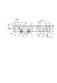
次に、本発明の第2の実施形態に係る光デバイスである光変調器800について説明する。図8は、本発明の第2の実施形態に係る光デバイスである光変調器800の構成を示す図である。図8においては、上から順に、光変調器800の平面図、側面820の側の側面図、底面図、及び側面822の側の側面図、である。[Second embodiment]
Next, an
この光変調器800は、例えば光伝送システムを構成する光送信装置に用いられる。なお、光変調器800は、本発明に係る光デバイスの一例であって、以下に示す光変調器100の構成は、筐体内に光機能素子を備えて当該筐体に光の入出射を行う光ファイバや電気端子が設けられる光デバイスにおいて広く一般に用いることができる。 This
光変調器800は、光機能素子である光変調素子802と、光変調素子802を収容する筐体804と、を備える。ここで、筐体804は、例えば、平面視が略長方形であり、長辺側側面と短辺側側面を有する。また、光変調器800は、筐体804の外部から光変調素子802に光を入射するための入力用光ファイバである光ファイバ808と、光変調素子802から出力される光を筐体804の外部へ導く出力用光ファイバである光ファイバ810と、を備える。 The
筐体804は、光変調素子802が固定されるケース814aとカバー814bとで構成されている。なお、筐体804内部における構成の理解を容易するため、図8においては、カバー814bの一部のみを図示左方に示しているが、実際には、カバー814bは、箱状のケース814aの全体を覆うように配されて筐体104の内部を気密封止する。ここで、図8の最上段に示す光変調器800の平面図において、筐体804の図示下側の側面を側面820、図示上側の側面を側面822と称する。 The housing 804 is composed of a
光変調素子802は、例えばLN基板上に設けられた4つのマッハツェンダ型光導波路と、当該マッハツェンダ型光導波路上にそれぞれ設けられて光導波路内を伝搬する光波を変調する4つのRF電極(高周波電極)(不図示)と、を備えたDP―QPSK光変調器である。 The
光変調素子802に設けられた上記4つのRF電極のそれぞれは、中継基板812に形成された導体パターン(不図示)を介して4つのリードピン830、832、834、836と電気的に接続されている。リードピン830、832、834、836は、筐体804の底面880を通って筐体804の外部まで延在し、FPC(フレキシブルプリント板)850に設けられた導体パターン(不図示)と、例えばハンダにより電気的に接続されている。また、筐体804(詳細には、ケース814a)の底面880には、リードピン830、832、834、836が設けられた部分(すなわち、これらのリードピン830等が筐体804から筐体804の外部へ延在する部分)に、凹部860が形成されており、FPC850は、当該凹部860の側面820側の開口部から筐体804の側方へ延在している。ここで、凹部860は、筐体804の外部と光変調素子802との間で電気信号の入力を行うための凹部に相当する。 Each of the four RF electrodes provided on the
特に、光変調器800では、筐体804の底面880において、電気端子であるリードピン830等が設けられた部分に形成された凹部860に対し、筐体804の幅方向に対する中心線870を挟んで対向する位置に、歪抑制手段である凹部862が形成されている。 In particular, in the
すなわち、光変調器800では、筐体804の外部と光変調素子802との間で電気信号の入力を行うための凹部860が設けられており、筐体804のうち凹部860が設けられた底面880には、当該凹部860に対し、底面880の平面視形状の中心線870を挟んで対称な位置に、歪抑制手段である凹部862が設けられている。 That is, the
これにより、光変調器800では、凹部860を設けることによる筐体804における機械強度低下部分の偏在を、凹部862を設けることにより防止することができる。その結果、上述した光変調器100等と同様に、筐体804における加工歪の集中や環境温度変動時の応力集中を防止して、より安定な光学特性を有する光変調器を実現することできる。尚、本実施形態で示したリードピンの数はこれに限定されない。 Accordingly, in the
また、本実施形態では筐体804の外部と光機能素子である光変調素子802との間で電気信号の入力を行うための一つの凹部860が底面880に設けられるものとしたが、これには限られない。例えば、筐体804の少なくとも一つの面に、筐体804の外部と光機能素子である光変調素子802との間で光及び又は電気信号の入出力を行うための孔及び又は凹部が設けられているものとしてもよい。 In this embodiment, one
この場合には、筐体804の上記孔及び又は凹部が設けられたそれぞれの面には、当該孔及び又は凹部に対し、当該面の平面視形状の中心線を挟んで対称な位置に、歪抑制手段である凹部が設けられるものとすることができる。尚、本実施例2の構成に前述の実施例1の構成を組み合わせてもよい。 In this case, on each surface of the housing 804 on which the holes and/or recesses are provided, strain is placed at positions symmetrical with respect to the holes and/or recesses across the center line of the plane view shape of the surface. A recess as a suppressing means may be provided. The configuration of the second embodiment may be combined with the configuration of the first embodiment.
なお、上述の各実施形態についての説明では所定の機能を有する光機能素子として光変調機能を有する光機能素子を例にあげて説明してきたが、本発明はこれに限定されない。例えば所定の機能を有する光機能素子には、波長変換素子として用いられるPPLNや空間光学結合系として用いるレンズなど、筐体における歪の偏在や環境温度変動時の応力の偏在により光学特性が変化し得る素子が含まれる。 In the description of each of the above-described embodiments, an optical functional element having a light modulating function has been exemplified as an optical functional element having a predetermined function, but the present invention is not limited to this. For example, optical functional elements with a predetermined function include PPLN used as a wavelength conversion element and lenses used as a spatial optical coupling system. It includes elements that can be obtained.
以上説明したように、本発明に従う光デバイスである光変調器100は、所定の機能を有する光機能素子である光変調素子102と、光変調素子102を収容する筐体104と、を備え、前記筐体の少なくとも一の側面112には、筐体104の外部と光変調素子102との間で光及び又は電気信号の入出力を行うための孔116等及び又は凹部130等が設けられており、筐体104の孔106等及び又は凹部130等が設けられた側面112の厚さに対し、当該側面112に対向する他の側面170の厚さが薄く構成されている。 As described above, the
本構成によれば、孔116等や凹部130等の加工が施されることにより機械強度が低下した筐体104の側面112の壁厚t1に対し、対向する側面170の壁厚t2を薄くすることで、これら対向する2つの側面112、170の機械強度を同程度のものとして、一方の側面に歪や応力が集中することによる筐体104の変形の発生を低減することができる。その結果、筐体104における歪の偏在や環境温度変動時の応力の偏在を抑制して、より安定な光学特性を実現することができる。 According to this configuration, the wall thickness t2 of the opposing
また、光変調器100の変形例である光変調器100-1では、筐体104-1の外部と光変調素子102との間で光及び又は電気信号の入出力を行うための孔116等及び又は凹部130等が設けられた側面112に対向する他の側面170には、歪抑制手段である凹部310等が設けられている。 Further, in the optical modulator 100-1, which is a modified example of the
この構成によれば、側面112に孔116等や凹部130等及び150等が設けられることにより当該側面112に生じる歪に対し、中心線350を挟んで当該歪とバランスする側面170の位置に歪抑制手段である凹部310等が設けられこととなる。その結果、光変調器100-1では、光変調器100と同様に、筐体104における歪の偏在や環境温度変動時の応力の偏在を抑制して、より安定な光学特性を実現することができる。 According to this configuration, the strain generated in the
また、光変調器100の変形例である光変調器100-2は、上記歪抑制手段である凹部310等を設けることに加えて、孔116等及び又は凹部130等が設けられた側面112の厚さに対し、当該側面112に対向する他の側面170の厚さが薄く構成されている。 Further, an optical modulator 100-2, which is a modified example of the
本構成によれば、光変調器100と同様に、筐体104-2における歪の偏在や環境温度変動時の応力の偏在を抑制して、より安定な光学特性を実現することができる。 According to this configuration, as in the case of the
また、光変調器100では、筐体104は、平面視が略矩形であって長辺側側面と短辺側側面とを有し、筐体104の長辺側側面である側面112に、孔116等並びに凹部130等及び150等が設けられている。この構成によれば、光変調器100を光送信装置の装置筐体内の角部に実装することができ、装置筐体内に各種部品を収容する際の空間利用率を向上することができる。 In the
また、光変調器100の変形例である光変調器100-3は、筐体104-3の外部と光変調素子102との間で光の入力を行う孔116及び光の出力を行う孔524が、筐体104-3の互いに隣接する2つの側面112及び572にそれぞれ設けられている。この構成によれば、光送信装置の装置筐体内における光変調器100-3の実装場所の自由度を向上して、装置筐体内に各種部品を収容する際の空間利用率を向上することができる。 Further, an optical modulator 100-3, which is a modified example of the
また、光変調器100では、筐体104の外部と光変調素子102との間で光の入出力を行うための孔116等と、筐体104の外部と光変調素子102との間で電気信号の入出力を行う電気端子を設けるための孔又は凹部130等が、筐体104の同じ側面112に設けられている。この構成によれば、光変調器100を光送信装置の装置筐体内の角部に実装することができ、装置筐体内に各種部品を収容する際の空間利用率を向上することができる。 In the
また、本発明に従う光デバイスである光変調器800は、光変調素子802と、光変調素子802を収容する筐体804と、を備え、筐体804の底面880には、筐体804の外部と光変調素子802との間で電気信号の入出力を行うための凹部860が設けられており、当該凹部860が設けられた底面880には、凹部862に対し、当該底面880の平面視形状の中心線870を挟んで対称な位置に、歪抑制手段である凹部862が設けられている。 Further,
この構成によれば、凹部860の加工が施されることにより機械強度が低下した筐体804の底面880の部分に対し、中心線870挟んで対向する底面880の部分に歪抑制手段である凹部862が設けられるので、底面880の一部に歪や応力が集中することによる筐体804の変形の発生を低減することができる。その結果、筐体804における歪の偏在や環境温度変動時の応力の偏在を抑制して、より安定な光学特性を実現することができる。 According to this configuration, the recessed portion, which is the distortion suppressing means, is formed in the portion of the
また、光変調器100等では、光機能素子は、光導波路と当該光導波路を伝搬する光波を制御する電極が設けられた光導波路素子である光変調素子102等である。この構成によれば、より安定な光学特性を有する光変調器を実現して、より安定な伝送品質を持つ光送信装置を実現することができる。 In the
100、100-1、100-2、100-3、100-4、800…光変調器、102、802…光変調素子、104、104-1、104-2、104-3、104-4、804…筐体、108、110、808、810…光ファイバ、112、170、572、574、820、822…側面、114a、114a-1、114a-2、114a-3、114a-4、814a…ケース、114b、814b…カバー、116、124、524…孔、120…マイクロレンズアレイ、122、122-3…偏波合成器、126…レンズ、130、132、134、136、150、152、154、310、312、314、316、410、412、414、416、712、860、862…凹部、140…RFコネクタ群、160、162、164…リードピン群、350、450、752…中心線、812…中継基板、830、832、834、836…リードピン、850…FPC、880…底面。
100, 100-1, 100-2, 100-3, 100-4, 800... optical modulator, 102, 802... optical modulation element, 104, 104-1, 104-2, 104-3, 104-4, 804... housing, 108, 110, 808, 810... optical fiber, 112, 170, 572, 574, 820, 822... side surface, 114a, 114a-1, 114a-2, 114a-3, 114a-4, 814a...
Claims (7)
Translated fromJapanese前記光機能素子を収容する筐体と、
を備え、
前記光機能素子は、光導波路と当該光導波路を伝搬する光波を制御する電極が設けられた光導波路素子であって、
前記筐体の少なくとも一の側面には、当該筐体の外部と前記光機能素子との間で光及び又は電気信号の入出力を行うための孔及び又は凹部が設けられており、
前記筐体の前記孔及び又は凹部が設けられたそれぞれの側面に対向する他の側面のそれぞれには、対応する前記孔及び又は凹部に対向する位置に、歪抑制手段である凹部が設けられている、
光デバイス。an optical functional element having a predetermined function;
a housing that houses the optical functional element;
with
The optical functional device is an optical waveguide device provided with an optical waveguide and an electrode for controlling a light wave propagating through the optical waveguide,
At least one side surface of the housing is provided with a hole and/or a recess for inputting/outputting light and/or electrical signals between the outside of the housing and the optical functional element,
Each of the other side surfaces of the housing, which face the side surfaces provided with the holes and/or recesses, is provided with a recess as a distortion suppressing means at a position facing the corresponding holeand /or recess. there is
optical device.
請求項1に記載の光デバイス。The recess, which is the distortion suppressing means, is provided on the inner surface of the housing among the other side surfaces,
The optical device according to claim 1.
請求項2に記載の光デバイス。The thickness of each side surface of the housing on which the holes and/or recesses are provided is thinner than the thickness of each side surface opposite to the side surface.
3. An optical device according to claim 2.
請求項1ないし3のいずれか一項に記載の光デバイス。A hole for inputting light and a hole for outputting light between the outside of the housing and the optical functional element are provided on the same side of the housing,
4. An optical device according to any one of claims 1 to 3.
請求項1ないし3のいずれか一項に記載の光デバイス。A hole for inputting light and a hole for outputting light between the outside of the housing and the optical functional element are provided on two side surfaces of the housing that are adjacent to each other,
4. An optical device according to any one of claims 1 to3 .
請求項4に記載の光デバイス。A hole and/or a recess for providing an electrical terminal for inputting and outputting an electrical signal between the outside of the housing and the optical functional element is provided on the same side surface of the housing.
5. An optical device according to claim 4.
前記光機能素子を収容する筐体と、
を備え、
前記光機能素子は、光導波路と当該光導波路を伝搬する光波を制御する電極が設けられた光導波路素子であって、
前記筐体の一の面には、当該筐体の外部と前記光機能素子との間で電気信号の入出力を行うための凹部が設けられており、
前記筐体の前記凹部が設けられた面には、当該凹部に対し、当該面の形状の中心線を挟んで対称な位置に、歪抑制手段である凹部が設けられている、
光デバイス。an optical functional element having a predetermined function;
a housing that houses the optical functional element;
with
The optical functional device is an optical waveguide device provided with an optical waveguide and an electrode for controlling a light wave propagating through the optical waveguide,
One surface of the housing is provided with a recess for inputting and outputting electrical signals between the outside of the housing and the optical functional element,
On the surface of the housing on which the recess is provided, a recess that is a distortion suppressing means is provided at a symmetrical position with respect to the recess across the center line of the shape of the surface.
optical device.
Priority Applications (1)
| Application Number | Priority Date | Filing Date | Title |
|---|---|---|---|
| JP2018066986AJP7139653B2 (en) | 2018-03-30 | 2018-03-30 | optical device |
Applications Claiming Priority (1)
| Application Number | Priority Date | Filing Date | Title |
|---|---|---|---|
| JP2018066986AJP7139653B2 (en) | 2018-03-30 | 2018-03-30 | optical device |
Publications (2)
| Publication Number | Publication Date |
|---|---|
| JP2019179085A JP2019179085A (en) | 2019-10-17 |
| JP7139653B2true JP7139653B2 (en) | 2022-09-21 |
Family
ID=68278527
Family Applications (1)
| Application Number | Title | Priority Date | Filing Date |
|---|---|---|---|
| JP2018066986AActiveJP7139653B2 (en) | 2018-03-30 | 2018-03-30 | optical device |
Country Status (1)
| Country | Link |
|---|---|
| JP (1) | JP7139653B2 (en) |
Citations (10)
| Publication number | Priority date | Publication date | Assignee | Title |
|---|---|---|---|---|
| JP2003043428A (en) | 2001-07-27 | 2003-02-13 | Fujikura Ltd | Thermo-optic effect optical components |
| JP2007003728A (en) | 2005-06-22 | 2007-01-11 | Fujitsu Ltd | Light intensity detector |
| CN201583684U (en) | 2009-09-01 | 2010-09-15 | 武汉光迅科技股份有限公司 | Temperature insensitive array wave guide grating packaging structure |
| JP2010276849A (en) | 2009-05-28 | 2010-12-09 | Sumitomo Osaka Cement Co Ltd | Optical element module |
| JP2012094627A (en) | 2010-10-26 | 2012-05-17 | Kyocera Corp | Package for housing element and electronic apparatus with the same |
| JP2012094701A (en) | 2010-10-27 | 2012-05-17 | Kyocera Corp | Package for housing semiconductor element and module including the package |
| JP2014049563A (en) | 2012-08-30 | 2014-03-17 | Kyocera Corp | Package for housing electronic component and mounting structure |
| US20150260921A1 (en) | 2014-03-17 | 2015-09-17 | Jds Uniphase Corporation | Optical switching device |
| JP2016191823A (en) | 2015-03-31 | 2016-11-10 | 住友大阪セメント株式会社 | Optical Modulator Module |
| JP2016206415A (en) | 2015-04-22 | 2016-12-08 | 富士通オプティカルコンポーネンツ株式会社 | Optical module and optical fiber assembly |
Family Cites Families (3)
| Publication number | Priority date | Publication date | Assignee | Title |
|---|---|---|---|---|
| JPS59159110A (en)* | 1983-02-28 | 1984-09-08 | Sumitomo Electric Ind Ltd | Adhesive structure for optical components |
| JPH0974248A (en)* | 1995-09-05 | 1997-03-18 | Toshiba Corp | Optical semiconductor module device |
| JPH10303508A (en)* | 1997-04-28 | 1998-11-13 | Hitachi Ltd | Package case and semiconductor module |
- 2018
- 2018-03-30JPJP2018066986Apatent/JP7139653B2/enactiveActive
Patent Citations (10)
| Publication number | Priority date | Publication date | Assignee | Title |
|---|---|---|---|---|
| JP2003043428A (en) | 2001-07-27 | 2003-02-13 | Fujikura Ltd | Thermo-optic effect optical components |
| JP2007003728A (en) | 2005-06-22 | 2007-01-11 | Fujitsu Ltd | Light intensity detector |
| JP2010276849A (en) | 2009-05-28 | 2010-12-09 | Sumitomo Osaka Cement Co Ltd | Optical element module |
| CN201583684U (en) | 2009-09-01 | 2010-09-15 | 武汉光迅科技股份有限公司 | Temperature insensitive array wave guide grating packaging structure |
| JP2012094627A (en) | 2010-10-26 | 2012-05-17 | Kyocera Corp | Package for housing element and electronic apparatus with the same |
| JP2012094701A (en) | 2010-10-27 | 2012-05-17 | Kyocera Corp | Package for housing semiconductor element and module including the package |
| JP2014049563A (en) | 2012-08-30 | 2014-03-17 | Kyocera Corp | Package for housing electronic component and mounting structure |
| US20150260921A1 (en) | 2014-03-17 | 2015-09-17 | Jds Uniphase Corporation | Optical switching device |
| JP2016191823A (en) | 2015-03-31 | 2016-11-10 | 住友大阪セメント株式会社 | Optical Modulator Module |
| JP2016206415A (en) | 2015-04-22 | 2016-12-08 | 富士通オプティカルコンポーネンツ株式会社 | Optical module and optical fiber assembly |
Also Published As
| Publication number | Publication date |
|---|---|
| JP2019179085A (en) | 2019-10-17 |
Similar Documents
| Publication | Publication Date | Title |
|---|---|---|
| CN111512218B (en) | Optical module and assembly method thereof | |
| JP6398318B2 (en) | Optical transceiver | |
| US10558064B2 (en) | Optical communication module and optical modulator used therein | |
| US9473245B2 (en) | Optical module including semiconductor optical modulator | |
| JP7030417B2 (en) | Optical subassemblies, optical modules, and optical transmitters | |
| JPWO2019044442A1 (en) | Pluggable optical module and optical communication system | |
| JP2020003701A (en) | Optical modulator and optical module using the same | |
| CN113228303A (en) | Optical module | |
| JP5861724B2 (en) | Optical device | |
| CN111679457B (en) | Optical modulator and optical transmission device using the same | |
| CN113424087B (en) | Optical module | |
| US11397364B2 (en) | Optical modulator and optical transmission apparatus | |
| JP7139653B2 (en) | optical device | |
| JP6223671B2 (en) | Optical module | |
| CN112639587B (en) | Optical modulator and optical module using the same | |
| JP7495359B2 (en) | Optical Modules | |
| US20220369524A1 (en) | Optical module and method of manufacturing optical module | |
| JP2022037163A (en) | Optical subassemblies, optical modules, and optical transmitters | |
| JP6216902B2 (en) | Optical module | |
| JP2016072920A (en) | Optical transceiver | |
| CN112352190B (en) | Optical modulator and optical module using the same | |
| JP7196424B2 (en) | optical module | |
| JP2015210457A (en) | Optical module and assembly method of optical module | |
| KR20230032819A (en) | Multi-channel Optical Sub-Assembly |
Legal Events
| Date | Code | Title | Description |
|---|---|---|---|
| A621 | Written request for application examination | Free format text:JAPANESE INTERMEDIATE CODE: A621 Effective date:20200805 | |
| A977 | Report on retrieval | Free format text:JAPANESE INTERMEDIATE CODE: A971007 Effective date:20210531 | |
| A131 | Notification of reasons for refusal | Free format text:JAPANESE INTERMEDIATE CODE: A131 Effective date:20210706 | |
| A521 | Request for written amendment filed | Free format text:JAPANESE INTERMEDIATE CODE: A523 Effective date:20210906 | |
| A131 | Notification of reasons for refusal | Free format text:JAPANESE INTERMEDIATE CODE: A131 Effective date:20220118 | |
| A521 | Request for written amendment filed | Free format text:JAPANESE INTERMEDIATE CODE: A523 Effective date:20220307 | |
| A131 | Notification of reasons for refusal | Free format text:JAPANESE INTERMEDIATE CODE: A131 Effective date:20220607 | |
| A521 | Request for written amendment filed | Free format text:JAPANESE INTERMEDIATE CODE: A523 Effective date:20220802 | |
| TRDD | Decision of grant or rejection written | ||
| A01 | Written decision to grant a patent or to grant a registration (utility model) | Free format text:JAPANESE INTERMEDIATE CODE: A01 Effective date:20220809 | |
| A61 | First payment of annual fees (during grant procedure) | Free format text:JAPANESE INTERMEDIATE CODE: A61 Effective date:20220822 | |
| R150 | Certificate of patent or registration of utility model | Ref document number:7139653 Country of ref document:JP Free format text:JAPANESE INTERMEDIATE CODE: R150 |