JP7139261B2 - semiconductor equipment - Google Patents
semiconductor equipmentDownload PDFInfo
- Publication number
- JP7139261B2 JP7139261B2JP2019011905AJP2019011905AJP7139261B2JP 7139261 B2JP7139261 B2JP 7139261B2JP 2019011905 AJP2019011905 AJP 2019011905AJP 2019011905 AJP2019011905 AJP 2019011905AJP 7139261 B2JP7139261 B2JP 7139261B2
- Authority
- JP
- Japan
- Prior art keywords
- signal
- polarity
- circuit
- rewrite
- stop
- Prior art date
- Legal status (The legal status is an assumption and is not a legal conclusion. Google has not performed a legal analysis and makes no representation as to the accuracy of the status listed.)
- Active
Links
Images


Classifications
- G—PHYSICS
- G05—CONTROLLING; REGULATING
- G05B—CONTROL OR REGULATING SYSTEMS IN GENERAL; FUNCTIONAL ELEMENTS OF SUCH SYSTEMS; MONITORING OR TESTING ARRANGEMENTS FOR SUCH SYSTEMS OR ELEMENTS
- G05B19/00—Programme-control systems
- G05B19/02—Programme-control systems electric
- G05B19/04—Programme control other than numerical control, i.e. in sequence controllers or logic controllers
- G05B19/042—Programme control other than numerical control, i.e. in sequence controllers or logic controllers using digital processors
- G05B19/0423—Input/output
- G—PHYSICS
- G09—EDUCATION; CRYPTOGRAPHY; DISPLAY; ADVERTISING; SEALS
- G09G—ARRANGEMENTS OR CIRCUITS FOR CONTROL OF INDICATING DEVICES USING STATIC MEANS TO PRESENT VARIABLE INFORMATION
- G09G3/00—Control arrangements or circuits, of interest only in connection with visual indicators other than cathode-ray tubes
- G09G3/20—Control arrangements or circuits, of interest only in connection with visual indicators other than cathode-ray tubes for presentation of an assembly of a number of characters, e.g. a page, by composing the assembly by combination of individual elements arranged in a matrix no fixed position being assigned to or needed to be assigned to the individual characters or partial characters
- G09G3/34—Control arrangements or circuits, of interest only in connection with visual indicators other than cathode-ray tubes for presentation of an assembly of a number of characters, e.g. a page, by composing the assembly by combination of individual elements arranged in a matrix no fixed position being assigned to or needed to be assigned to the individual characters or partial characters by control of light from an independent source
- G09G3/36—Control arrangements or circuits, of interest only in connection with visual indicators other than cathode-ray tubes for presentation of an assembly of a number of characters, e.g. a page, by composing the assembly by combination of individual elements arranged in a matrix no fixed position being assigned to or needed to be assigned to the individual characters or partial characters by control of light from an independent source using liquid crystals
- G09G3/3611—Control of matrices with row and column drivers
- G09G3/3614—Control of polarity reversal in general
- G—PHYSICS
- G09—EDUCATION; CRYPTOGRAPHY; DISPLAY; ADVERTISING; SEALS
- G09G—ARRANGEMENTS OR CIRCUITS FOR CONTROL OF INDICATING DEVICES USING STATIC MEANS TO PRESENT VARIABLE INFORMATION
- G09G3/00—Control arrangements or circuits, of interest only in connection with visual indicators other than cathode-ray tubes
- G09G3/20—Control arrangements or circuits, of interest only in connection with visual indicators other than cathode-ray tubes for presentation of an assembly of a number of characters, e.g. a page, by composing the assembly by combination of individual elements arranged in a matrix no fixed position being assigned to or needed to be assigned to the individual characters or partial characters
- G09G3/34—Control arrangements or circuits, of interest only in connection with visual indicators other than cathode-ray tubes for presentation of an assembly of a number of characters, e.g. a page, by composing the assembly by combination of individual elements arranged in a matrix no fixed position being assigned to or needed to be assigned to the individual characters or partial characters by control of light from an independent source
- G09G3/36—Control arrangements or circuits, of interest only in connection with visual indicators other than cathode-ray tubes for presentation of an assembly of a number of characters, e.g. a page, by composing the assembly by combination of individual elements arranged in a matrix no fixed position being assigned to or needed to be assigned to the individual characters or partial characters by control of light from an independent source using liquid crystals
- G09G3/3611—Control of matrices with row and column drivers
- G09G3/3685—Details of drivers for data electrodes
- G09G3/3688—Details of drivers for data electrodes suitable for active matrices only
- G—PHYSICS
- G09—EDUCATION; CRYPTOGRAPHY; DISPLAY; ADVERTISING; SEALS
- G09G—ARRANGEMENTS OR CIRCUITS FOR CONTROL OF INDICATING DEVICES USING STATIC MEANS TO PRESENT VARIABLE INFORMATION
- G09G3/00—Control arrangements or circuits, of interest only in connection with visual indicators other than cathode-ray tubes
- G09G3/20—Control arrangements or circuits, of interest only in connection with visual indicators other than cathode-ray tubes for presentation of an assembly of a number of characters, e.g. a page, by composing the assembly by combination of individual elements arranged in a matrix no fixed position being assigned to or needed to be assigned to the individual characters or partial characters
- G09G3/34—Control arrangements or circuits, of interest only in connection with visual indicators other than cathode-ray tubes for presentation of an assembly of a number of characters, e.g. a page, by composing the assembly by combination of individual elements arranged in a matrix no fixed position being assigned to or needed to be assigned to the individual characters or partial characters by control of light from an independent source
- G09G3/36—Control arrangements or circuits, of interest only in connection with visual indicators other than cathode-ray tubes for presentation of an assembly of a number of characters, e.g. a page, by composing the assembly by combination of individual elements arranged in a matrix no fixed position being assigned to or needed to be assigned to the individual characters or partial characters by control of light from an independent source using liquid crystals
- G09G3/3611—Control of matrices with row and column drivers
- G09G3/3696—Generation of voltages supplied to electrode drivers
- G—PHYSICS
- G05—CONTROLLING; REGULATING
- G05B—CONTROL OR REGULATING SYSTEMS IN GENERAL; FUNCTIONAL ELEMENTS OF SUCH SYSTEMS; MONITORING OR TESTING ARRANGEMENTS FOR SUCH SYSTEMS OR ELEMENTS
- G05B2219/00—Program-control systems
- G05B2219/20—Pc systems
- G05B2219/25—Pc structure of the system
- G05B2219/25257—Microcontroller
- G—PHYSICS
- G09—EDUCATION; CRYPTOGRAPHY; DISPLAY; ADVERTISING; SEALS
- G09G—ARRANGEMENTS OR CIRCUITS FOR CONTROL OF INDICATING DEVICES USING STATIC MEANS TO PRESENT VARIABLE INFORMATION
- G09G2310/00—Command of the display device
- G09G2310/02—Addressing, scanning or driving the display screen or processing steps related thereto
- G09G2310/0264—Details of driving circuits
- G09G2310/0291—Details of output amplifiers or buffers arranged for use in a driving circuit
- G—PHYSICS
- G09—EDUCATION; CRYPTOGRAPHY; DISPLAY; ADVERTISING; SEALS
- G09G—ARRANGEMENTS OR CIRCUITS FOR CONTROL OF INDICATING DEVICES USING STATIC MEANS TO PRESENT VARIABLE INFORMATION
- G09G2310/00—Command of the display device
- G09G2310/08—Details of timing specific for flat panels, other than clock recovery
- G—PHYSICS
- G09—EDUCATION; CRYPTOGRAPHY; DISPLAY; ADVERTISING; SEALS
- G09G—ARRANGEMENTS OR CIRCUITS FOR CONTROL OF INDICATING DEVICES USING STATIC MEANS TO PRESENT VARIABLE INFORMATION
- G09G2320/00—Control of display operating conditions
- G09G2320/02—Improving the quality of display appearance
- G09G2320/0257—Reduction of after-image effects
Landscapes
- Engineering & Computer Science (AREA)
- Physics & Mathematics (AREA)
- General Physics & Mathematics (AREA)
- Chemical & Material Sciences (AREA)
- Crystallography & Structural Chemistry (AREA)
- Computer Hardware Design (AREA)
- Theoretical Computer Science (AREA)
- Automation & Control Theory (AREA)
- Control Of Indicators Other Than Cathode Ray Tubes (AREA)
- Liquid Crystal Display Device Control (AREA)
- Liquid Crystal (AREA)
Description
Translated fromJapanese本開示は、半導体装置に関し、特に、表示装置を制御するマイクロコントローラ等の半導体集積回路装置に適用可能である。 The present disclosure relates to semiconductor devices, and is particularly applicable to semiconductor integrated circuit devices such as microcontrollers that control display devices.
液晶表示パネルを利用した表示装置では、画面の焼き付きを防止するため、画素の共通電極に供給される電位(VCOM電位)を時間的に変化させる技術が知られている。特開2018-132716号公報(特許文献1)は、「CPU101は、極性を反転すべきタイミングが、画像データが出力されている期間内である場合、当該タイミング当該期間の後のタイミングに変更する。」を開示している。 2. Description of the Related Art In a display device using a liquid crystal display panel, there is known a technique of temporally changing the potential (VCOM potential) supplied to a common electrode of pixels in order to prevent screen burn-in. Japanese Patent Laying-Open No. 2018-132716 (Patent Document 1) states, "When the timing at which the polarity should be reversed is within a period during which image data is being output, the CPU 101 changes the timing to a timing after the period. .”
マイクロコントローラ等の半導体装置は、表示装置に表示される表示データを書き換えるため、表示データの書き替え動作を行う。表示データの書き替え動作は、表示装置の仕様を満足するように行う必要がある。表示データの書き替え動作が、表示装置の仕様を満足しなかった場合、表示装置の表示品質が低下してしまう場合がある。 A semiconductor device such as a microcontroller rewrites display data to rewrite display data displayed on the display device. The display data rewriting operation must be performed so as to satisfy the specifications of the display device. If the display data rewriting operation does not satisfy the specifications of the display device, the display quality of the display device may deteriorate.
本開示の課題は、表示装置の表示品質が低下を抑制しつつ、表示装置に対する表示データの書き替えを行う技術を提供することにある。 An object of the present disclosure is to provide a technique for rewriting display data on a display device while suppressing deterioration in display quality of the display device.
その他の課題と新規な特徴は、本明細書の記述および添付図面から明らかになるであろう。 Other problems and novel features will become apparent from the description of the specification and the accompanying drawings.
本開示のうち代表的なものの概要を簡単に説明すれば下記の通りである。 A brief outline of a representative one of the present disclosure is as follows.
すなわち、半導体装置は、表示制御装置を含む。前記表示制御装置は、一定周期の信号に基づいて、交流信号の極性を前記周期で反転させて出力する出力部と、停止信号に基づいて、前記交流信号出力部における前記交流信号の極性の反転を停止させる停止制御部と、表示データ書き換え信号を出力する書き換え制御部と、前記書き換え制御部を制御する送信制御部と、を含む。前記停止信号は、前記表示データ書き換え信号が出力される期間において、前記交流信号の極性の反転を停止させ、極性の反転を停止された前記交流信号は、極性の反転の停止の前の極性を維持する。前記出力部は、前記表示データ書き換え信号が出力される期間の後、一定周期の前記信号に基づいて、前記交流信号の極性を前記周期で反転させて出力する。 That is, the semiconductor device includes a display control device. The display control device includes an output unit that inverts the polarity of an AC signal in the cycle based on a signal of a constant cycle and outputs the AC signal, and the polarity of the AC signal in the AC signal output unit based on the stop signal. , a rewrite control unit that outputs a display data rewrite signal, and a transmission control unit that controls the rewrite control unit. The stop signal stops reversing the polarity of the AC signal during the period in which the display data rewriting signal is output, and the AC signal whose polarity is stopped has the polarity before the polarity reversal is stopped. maintain. After a period in which the display data rewrite signal is output, the output section inverts the polarity of the AC signal at the cycle based on the signal at the constant cycle and outputs the AC signal.
上記半導体装置よれば、表示装置の表示品質の低下を抑制しつつ、表示装置に対する表示データの書き替えを行うことが可能である。 According to the above semiconductor device, it is possible to rewrite display data for the display device while suppressing degradation of display quality of the display device.
以下、実施形態、および、実施例について、図面を用いて説明する。ただし、以下の説明において、同一構成要素には同一符号を付し繰り返しの説明を省略することがある。なお、図面は説明をより明確にするため、実際の態様に比べ、模式的に表される場合があるが、あくまで一例であって、本発明の解釈を限定するものではない。 Hereinafter, embodiments and examples will be described with reference to the drawings. However, in the following description, the same components may be denoted by the same reference numerals, and repeated descriptions may be omitted. In addition, in order to clarify the description, the drawings may be represented schematically as compared with actual embodiments, but they are only examples and do not limit the interpretation of the present invention.
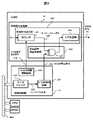
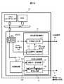
図1は、実施例1に係る半導体システムを示す図である。半導体システム1は、たとえば、電子時計、商品価格などを表示するタグ装置などの表示パネルを有する電子装置である。半導体システム1は、半導体装置10と、表示パネルを有する液晶表示装置20と、を有する。 FIG. 1 is a diagram showing a semiconductor system according to a first embodiment. The
半導体装置10は、マイクロコントローラMCUであり、たとえば、単結晶シリコンなどの半導体基板に、公知のCMOSトランジスタの製造方法を用いて形成された半導体集積回路装置である。半導体装置10としてのマイクロコントローラMCUは、制御部としての中央処理装置CPUと、不揮発性メモリROMと、揮発性メモリRAMと、データ転送制御装置DMACと、表示制御装置LCDCと、バスBUSと、を有する。バスBUSは、中央処理装置CPUと、不揮発性メモリROMと、揮発性メモリRAMと、データ転送制御装置DMACと、表示制御装置LCDCと、を相互に接続する。 The
中央処理装置CPUは、各種演算処理を行い、半導体システム1の全体動作を統括制御するプロセッサである。中央処理装置CPUは、不揮発性メモリROMから制御プログラムを読み出し、揮発性メモリRAMに格納して各種機能に係る演算制御や表示制御など各種動作処理を行う。 The central processing unit CPU is a processor that performs various kinds of arithmetic processing and controls the overall operation of the
不揮発性メモリROMは、たとえば、リードオンリメモリやフラッシュメモリなどにより構成することができる。不揮発性メモリROMは、制御プログラム、演算に必要とされるデータ、初期設定データ等が格納される。 The nonvolatile memory ROM can be composed of, for example, read-only memory or flash memory. The nonvolatile memory ROM stores control programs, data required for calculation, initial setting data, and the like.
揮発性メモリRAMは、たとえば、スタティック型ランダムアクセスメモリ(SRAM)やダイナミック型ランダムアクセスメモリ(DRAM)などにより構成することができる。揮発性メモリRAMは、たとえば、制御プログラムを実行する中央処理装置CPUの一時データの格納領域として利用される。 The volatile memory RAM can be composed of, for example, static random access memory (SRAM) or dynamic random access memory (DRAM). The volatile memory RAM is used, for example, as a temporary data storage area for the central processing unit CPU that executes the control program.
データ転送制御装置DMACは、たとえば、ダイレクトメモリアクセスコントローラにより構成することができる。データ転送制御装置DMACは、中央処理装置CPUの介在なしに、メモリとメモリとの間、または、メモリと周辺回路または周辺機器との間で直接データの転送の制御を行う。データ転送制御装置DMACは、液晶表示装置20に表示する表示データの転送に利用することができる。 The data transfer control device DMAC can be composed of, for example, a direct memory access controller. The data transfer control unit DMAC controls direct data transfers between memories or between memories and peripheral circuits or peripheral devices without the intervention of the central processing unit CPU. The data transfer control device DMAC can be used to transfer display data to be displayed on the liquid
表示制御装置LCDCは、液晶表示装置20を制御する周辺回路であり、送信制御部11と、交流信号生成部12と、書き替え制御部13と、を含む。送信制御部11は、交流信号生成部12および書き替え制御部13の動作を制御する。 The display control device LCDC is a peripheral circuit that controls the liquid
交流信号生成部12は、VCOM信号14を生成し、液晶表示装置20へ出力する。VCOM信号14は、液晶表示装置20に設けられた液晶表示パネルの画面の焼き付きを防止するために利用される。VCOM信号14は、一例では、周期的にその極性が反転される交流電圧信号である。液晶表示装置20は、VCOM信号14の極性の反転タイミングに基づいて、複数の画素の共通電極に供給される共通電位(VCOM電位)の極性を、正電位から負電位へ、または、負電位から正電位へ変化させる。 The
書き替え制御部13は、表示データ書き替え信号15を生成し、液晶表示装置20へ出力する。表示データ書き替え信号15は、たとえば、書き替える表示データと、同期信号と、書き込みイネーブル信号(ライトイネーブル信号)などを含む。液晶表示装置20は、表示データ書き替え信号15に基づいて、液晶表示装置20内の対応する複数の画素の表示データを書き替える。 The
液晶表示装置20は、液晶表示パネルを有する表示装置である。液晶表示装置20は、一例では、複数の画素のそれぞれが表示データを記憶するメモリ素子を含むMIP(Memory In Pixel)液晶装置とすることができる。MIP液晶装置は、一般的なTFT(Thin Film Transistor)液晶装置と比較して、頻繁な書き替えを必要とせず、半導体システム1の低消費電力化を図ることができる。 The liquid
図2は、図1の表示制御装置の概念的な構成例を説明する図である。図2の表示制御装置LCDCに示す様に、交流信号生成部12は、交流信号出力部121と、交流信号停止制御部122と、を含む。交流信号出力部121は、交流信号生成クロックCKに基づいて、一定周期のVCOM信号14を生成し、液晶表示装置20へ送出する。交流信号停止制御部122は、送信制御部11で生成されるVCOM停止信号111に基づいて、VCOM信号14の極性の変化を停止させるためのVCOM停止指示信号123を交流信号出力部121へ送出する。交流信号出力部121は、VCOM停止指示信号123に基づいて、VCOM信号14の極性の変化を停止させる様に構成される。 FIG. 2 is a diagram for explaining a conceptual configuration example of the display control device in FIG. As shown in the display control device LCDC of FIG. 2 , the AC
書き替え制御部13は、表示データ生成部131、および、表示データ書き替え信号生成部132と、を含む。表示データ生成部131と表示データ書き替え信号生成部132によって生成された表示データ書き替え信号15を液晶表示装置20に送出する。 The
送信制御部11は、表示書き替えデータ116を表示データ生成部131へ出力し、送信開始指示信号117を表示データ書き替え信号生成部132へ出力する。 The
図3は、図2の送信制御部11、交流信号出力部121、交流信号停止制御部122の詳細な構成例を示す図である。 FIG. 3 is a diagram showing a detailed configuration example of the
送信制御部11は、データバッファ回路112と、トリガ検知回路113と、VCOM周期制御回路114と、を含む。データバッファ回路112は、バスBUSに接続され、中央処理装置CPUまたはデータ転送制御装置DMACにより表示書き替えデータが格納される。データバッファ回路112は、表示書き替えデータの書き込み量がデータバッファ回路112の記憶容量に一致すると、バッファフル信号115を生成する。トリガ検知回路113は、バッファフル信号115が入力されると、VCOM停止信号111を交流信号停止制御部122に発行する。VCOM周期制御回路114は、カウンタ124の基準カウント値を制御するために設けられる。カウンタ124の基準カウント値は、半導体装置10に接続される液晶表示装置20の種類に基づいて、VCOM周期制御回路114によって設定することが可能である。 The
交流信号出力部121は、カウンタ124と、トグル回路125と、を含む。交流信号停止制御部122は、AND回路127を含む。カウンタ124は、交流信号生成クロックCKを計数し、交流信号生成クロックCKの計数値が基準カウント値に一致すると、たとえば、ハイレベルのオーバーフロー信号126を発生する。カウンタ124は、オーバーフロー信号126の発生に基づいて、交流信号生成クロックCKの計数値をリセットし、再度、交流信号生成クロックCKの計数を開始する。AND回路127は、オーバーフロー信号126が入力される第1入力と、VCOM停止信号111の反転信号が入力される第2入力と、を有する。AND回路127の出力はトグル回路125の入力に接続されており、トグル回路125の出力はVCOM信号14とされている。 AC
AND回路127は、VCOM停止信号111がハイレベルとされると、ハイレベルのオーバーフロー信号126のトグル回路125への出力を禁止する。したがって、VCOM停止信号111がハイレベルとされた場合、トグル回路125の出力であるVCOM信号14の極性は変更されず、その極性は維持されることになる。 The AND
次に、動作を説明する。液晶表示装置20の表示データを書き替える際、中央処理装置CPUまたはデータ転送制御装置DMACにより表示書き替えデータの更新をするため、データバッファ回路112の書き替えを実施する。送信制御部11はデータバッファ回路112の書き替えにより発生したバッファフル信号115等をトリガ検知回路113が受け取り、交流信号停止制御部122にVCOM停止信号111を発行する。 Next, the operation will be explained. When rewriting the display data of the liquid
交流信号停止制御部122は、VCOM停止信号111により、VCOM信号14の極性の変化動作を停止する。この時、カウンタ124は、交流信号生成クロックCKによる計数動作を継続しているので、VCOM停止信号111による影響を受けずに、VCOM信号14の極性反転の変化タイミングを維持する。つまり、VCOM信号14の極性反転の変化タイミングを決めているカウンタ124のオーバーフロー信号126は、一定周期(T)で継続的に出力されていることになる。 The AC signal
VCOM信号14の極性反転の変化動作を停止(VCOM信号14の状態保持)する事で、液晶表示装置20に対するVCOM信号14の極性反転の変化時の制約無く、液晶表示装置20の表示データを書き替えが可能となる。 By stopping the changing operation of the polarity reversal of the VCOM signal 14 (holding the state of the VCOM signal 14), the display data of the liquid
また、交流信号出力部121のカウンタ124はVCOM周期制御回路114により基準カウント値(オーバーフローカウント値)を可変することで、一定周期(T)の送信に対するVCOM信号14の極性反転の変化動作の停止の連続を回避可能とするのが良い。つまり、オーバーフロー信号126の出力タイミングは、一定周期の表示書き替えデータの送信を考慮して決めるのが良い。なるべく、表示書き替えデータの更新の期間がVCOM信号14の極性反転の変化動作と重ならないように、基準カウント値を決めるのが良い。なお、基準カウント値は、各種の電子装置、各種の液晶表示装置に対応させるために、VCOM周期制御回路114によって変更可能に構成されている。基準カウント値は、一例では、VCOM信号14の極性の反転タイミングの周期Tが、0.5秒、1秒、2秒、または、5秒となるように、VCOM周期制御回路114により設定することが可能である。特に制限されるわけではないが、1つの電子装置に対していったん決めた基準カウント値は変更しないのが前提である。ただし、いったん決めた基準カウント値は、もちろん、変更されてもよい。 In addition, by varying the reference count value (overflow count value) of the counter 124 of the AC
次に、液晶表示装置20の仕様について説明する。図4は、図1の液晶表示装置20の仕様を説明する図である。液晶表示装置20は、VCOM信号14のハイレベルの幅(または期間)tHとロウレベルの幅(または期間)tLについて、最小値(tMIN)が仕様として規定されている場合がある。この場合、VCOM信号14のハイレベルの幅(または期間)tHとロウレベルの幅(または期間)tLは、最小値(tMIN)以上に設定する必要がある(tH>tMIN,tL>tMIN)。VCOM信号14のハイレベルの幅tHやロウレベルの幅tLが、規定された最小値(tMIN)以下の幅(または期間)になる(tH<tMIN、tL<tMIN)と、液晶表示装置20は、その液晶の特性を維持できなくなり、液晶表示装置20の表示品質が低下してしまう虞がある。 Next, specifications of the liquid
また、VCOM信号14の極性が反転されるタイミングの前後において、表示データの書き替えを禁止する書き替えを禁止期間tRWPが仕様として規定されている場合がある。つまり、VCOM信号14のロウレベルからハイレベルへ遷移する極性の反転タイミングとVCOM信号14のハイレベルからロウレベルへ遷移する極性の反転タイミングとの各々の前後において、書き替えを禁止期間tRWPが設けられる。書き替えを禁止期間tRWPにおいて、表示データの書き替えを実施すると、表示データが損失する場合や表示データが正常に表示されない場合がある。したがって、書き替えを禁止期間tRWPの間において、表示データの書き替えを実施する必要がある。 In some cases, a rewrite prohibition period tRWP for prohibiting rewriting of display data is specified as a specification before and after the timing at which the polarity of the
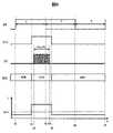
次に、表示データ書き替え信号の期間とVCOM信号14の極性の反転タイミングとの関係を説明する。図5は、表示データ書き替え信号15とVCOM信号14の極性の反転タイミングとが重ならない場合を示す図である。図6は、表示データ書き替え信号15とVCOM信号14の極性の反転タイミングとが重なった場合を示す図である。なお、図5および図6は、図4で説明された液晶表示装置20の仕様を満足しているものとする。 Next, the relationship between the period of the display data rewrite signal and the polarity reversal timing of the
図5を参照し、VCOM信号14は、時刻t1、t6、t7において、その極性が反転される反転タイミングを有する。VCOM信号14の極性の反転タイミングのおのおのは、タイマ回路124のオーバーフロー信号126の発生タイミングに基づいており、一定の周期Tで発生する。なお、周期Tは、図4の最小値(tMIN)より長くされている(T>tMIN)。 Referring to FIG. 5,
時刻t2において、VCOM停止信号111がロウレベルからハイレベルへ遷移し、時刻t3から時刻t4において、表示データ書き替え信号15が液晶表示装置20へ出力される。なお、表示データ書き替え信号15の出力されている期間TD(時刻t3~時刻t4の期間)は、周期Tより短くされる(TD<T)。なお、図5において、時刻t1~時刻t2の期間は、図4の書き替えを禁止期間tRWPの半分の期間(tRWP/2)よりも、長く設定されている。 At time t2, the VCOM stop signal 111 transitions from low level to high level, and the display
時刻t5において、VCOM停止信号111がハイレベルからロウレベルへ遷移し、表示データ書き替えが完了する。なお、VCOM停止信号111がハイレベルからロウレベルへ遷移は、表示データ書き替え信号15の出力が完了した時刻t4とされてもよい。なお、図5において、時刻t5~時刻t6の期間は、図4の書き替えを禁止期間tRWPの半分の期間(tRWP/2)よりも、長く設定されている。 At time t5, the VCOM stop signal 111 transitions from high level to low level, and rewriting of display data is completed. The transition of the VCOM stop signal 111 from high level to low level may be set at time t4 when output of the display
図5において、半導体装置10としてのマイクロコントローラMCUの動作モードMDは、時刻t2において、低消費電力なスタンバイ状態stbからアクティブ状態actへ移行し、時刻t5において、アクティブ状態actからスタンバイ状態stbへ移行する。すなわち、マイクロコントローラMCUは、この例では、VCOM停止信号111がハイレベル期間において、間欠的に、または、選択的に、アクティブ状態actへ移行し、その他の期間は低消費電力なスタンバイ状態stbにされている。したがって、マイクロコントローラMCUの消費電力Iは、アクティブ状態actの期間において、スタンバイ状態stbの期間と比較して、高くされる。図5において、Iac1は、マイクロコントローラMCUの平均消費電力を示しており、低く抑えられている。したがって、マイクロコントローラMCUが電池などのバッテリで駆動される場合、データ書き替え時間を短くすることで、マイクロコントローラMCUの平均消費電力を低くすることができるので、バッテリによるマイクロコントローラMCUの駆動時間を比較的長くすることができる。 In FIG. 5, the operation mode MD of the microcontroller MCU as the
図6を参照し、VCOM信号14は、時刻t1、t6、t7において、その極性が反転される反転タイミングを有している。ただし、時刻ta(時刻t3<時刻ta<時刻t4)において、タイマ回路124のオーバーフロー信号126が発生されるが、ハイレベルのVCOM停止信号111によって、VCOM信号14の極性の反転が抑止されるので、VCOM信号14のハイレベルは、時刻t1から時刻t6まで、維持される。したがって、表示データ書き替え動作は、時刻taにおけるVCOM信号14の極性の反転によって阻止されることがなく、時刻t3から時刻t4の間に、確実に実行される。他の動作は、図5と同じであるので、説明は省略する。図6において、時刻t1~時刻t2の期間および時刻t5~時刻t6の期間のおのおのは、図4の書き替えを禁止期間tRWPの半分の期間(tRWP/2)よりも、長くされている。 Referring to FIG. 6, the
以上のように、表示データ書き替え信号15とVCOM信号14の極性の反転タイミング(時刻ta)とが重なった場合であっても、送信制御部11より発行されたVCOM停止信号111により、交流信号停止制御部122はVCOM信号14の変化を停止する。VCOM信号14の極性変化の停止により、液晶表示装置20に送られるVCOM信号14の状態がハイレベルまたはロウレベルに保持され、VCOM信号14の状態による液晶表示装置20の制約が無くなり、任意のタイミングで表示データの書き替えが可能となる。この結果、マイクロコントローラMCUのアクティブ状態actの期間が、延長されることなく、最小にできる。したがって、半導体システム1全体の平均消費電流の低減が実現可能となる。その結果、マイクロコントローラMCUが電池などのバッテリで駆動される場合、データ書き替え時間を短くすることで、マイクロコントローラMCUの平均消費電力を低くすることができるので、バッテリによるマイクロコントローラMCUの駆動時間を比較的長くすることができる。 As described above, even when the display
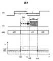
図7は、比較例に係る表示データ書き替え信号15とVCOM信号14の極性の反転タイミングとが重なった場合を示す図である。比較例では、時刻t10において、点線で示すように表示データ書き替え信号151を出力しようとしたが、時刻t11において、VCOM信号14の極性の反転タイミングが発生するため、表示データ書き替え信号15の出力の開始を、時刻t11以降の時刻t12へ遅延させる様に変更し、時刻t12~時刻t13において、表示データ書き替え動作を実施するものである。この場合、マイクロコントローラMCUのアクティブ状態actは、時刻t10から時刻t13の間のように、延長されることになる。したがって、半導体システム1全体の平均消費電流Iac2が増加してしまうことになる(Iac2>Iac1)。たとえば、マイクロコントローラMCUに、VCOM信号14の極性の反転タイミングを監視する監視回路を設け、監視回路の監視結果に基づいて、表示データ書き替え信号の出力の開始時刻を変更するようにすれば、図7に示す様な動作を行うことが可能である。 FIG. 7 is a diagram showing a case where the display
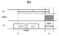
図8は、実施例1に係る複数回の表示データ書き替え動作を間欠的に行う場合を説明する図である。図9は、比較例2に係る複数回の表示データ書き替え動作を間欠的に行う場合を説明する図である。 8A and 8B are diagrams for explaining a case where display data rewrite operations are intermittently performed a plurality of times according to the first embodiment. FIG. 9 is a diagram for explaining a case in which display data rewrite operations are intermittently performed a plurality of times according to Comparative Example 2. In FIG.
図8に示されるVCOM信号14は、図6で説明した様に、時刻taにおいて、タイマ回路124のオーバーフロー信号126が発生されるが、ハイレベルのVCOM停止信号111によって、VCOM信号14の極性の反転が抑止され、VCOM信号14のハイレベルは、時刻taから時刻t6まで、維持される。時刻t6において、VCOM信号14はハイレベルからロウレベルへ遷移する極性の反転タイミングを有するので、図4で説明されたように、反転タイミングの前後において、表示データの書き替えを禁止する書き替え禁止期間tRWPが設けられることになる。 8, the overflow signal 126 of the timer circuit 124 is generated at time ta as described in FIG. Inversion is suppressed, and the high level of the
表示データの書き替え動作を間欠的に連続して2回行う場合を考える。たとえば、1回目の表示データ書き替え信号15_1の出力の完了した後、続いて、所定の時間経過後、2回目の表示データ書き替え信号15_2の出力を開始する。この場合、1回目の表示データ書き替え信号15_1の出力の完了と2回目の表示データ書き替え信号15_2の出力の開始との間の時間tdは、書き替え禁止期間tRWPを考慮することなく、比較的短い時間(最短時間)とすることができる。 Consider the case where the display data rewrite operation is intermittently performed twice in succession. For example, after the output of the display data rewrite signal 15_1 for the first time is completed, the output of the display data rewrite signal 15_2 for the second time is started after a predetermined time has passed. In this case, the time td between the completion of the output of the first display data rewrite signal 15_1 and the start of the second output of the display data rewrite signal 15_2 can be calculated without considering the rewrite prohibition period tRWP. can be set to a relatively short time (shortest time).
図9は、図8と同様に、表示データの書き替え動作を間欠的に連続して2回行う場合を示している。図9に示されるVCOM信号14は、時刻taにおいて、1回目の表示データ書き替え信号15_1の出力期間と重なるため、VCOM信号14のハイレベルからロウレベルへ遷移する極性の反転タイミングが時刻taから時刻tbへ変更される構成である。この構成は、たとえば、特開2018-132716号公報(特許文献1)に記載の技術を参照することができる。図4で説明されたように、時刻tbの反転タイミングの前後において、表示データの書き替えを禁止する書き替えを禁止期間tRWPが設けられる場合、2回目の表示データ書き替え信号15_2の出力の開始は、1回目の表示データ書き替え信号15_2の出力の完了後、書き替え禁止期間tRWPを経過した後に、行われることになる。したがって、1回目の表示データ書き替え信号15_1の出力の完了と2回目の表示データ書き替え信号15_2の出力の開始との間の時間(tRWP)は、図8に説明された構成(td)と比較し、長くなる(tRWP>td)。 Similar to FIG. 8, FIG. 9 shows a case where the display data rewrite operation is intermittently performed twice in succession. Since the
実施例1に従えば、1回目の表示データ書き替え動作と2回目の表示データ書き替え動作とが比較的短い時間(最短時間)で間欠的に連続して行うことができる。 According to the first embodiment, the first display data rewriting operation and the second display data rewriting operation can be performed intermittently and continuously in a relatively short time (shortest time).
図10は、実施例1に係る表示データ書き替え動作を説明する図である。図11は、比較例3に係る表示データ書き替え動作を説明する図である。 FIG. 10 is a diagram explaining a display data rewriting operation according to the first embodiment. 11A and 11B are diagrams for explaining a display data rewriting operation according to Comparative Example 3. FIG.
図10に示されるVCOM信号14は、図6で説明した様に、時刻taにおいて、タイマ回路124のオーバーフロー信号126が発生されるが、ハイレベルのVCOM停止信号111によって、VCOM信号14の極性の反転が抑止され、VCOM信号14のロウレベルは、時刻taから時刻t6まで、維持される。時刻t1と時刻taとの間、および時刻taと時刻t6との間は、タイマ回路124の出力するオーバーフロー信号126の発生タイミングに基づいて、周期Tとして設定される。つまり、周期Tは一定であるので、図4で説明した様に、VCOM信号14のハイレベルの幅(または期間)tHとロウレベルの幅(または期間)tLは、最小値(tMIN)以上に設定されていることになる。また、VCOM信号14の周期Tは必ず規定周期のN倍(Nは正の整数)になるため、液晶表示装置の仕様において、VCOM信号14のハイレベルの幅(または期間)tHとロウレベルの幅(または期間)tLは下限値(最小値tMIN)を考慮する必要が無い。 10, the overflow signal 126 of the timer circuit 124 is generated at time ta as described in FIG. Inversion is suppressed, and the low level of the
図11に示されるVCOM信号14は、時刻taにおいて、表示データ書き替え信号15_1の出力期間と重なるため、VCOM信号14のロウレベルからハイレベルへ遷移する極性の反転タイミングが時刻taから時刻tbへ変更される構成である。VCOM信号14は、また、時刻t6において、ハイレベルからロウレベルへ遷移する極性の反転タイミングを有する。ここで、時刻t1と時刻taとの間、および時刻taと時刻t6との間は、周期Tは一定である。この構成は、たとえば、特開2018-132716号公報(特許文献1)に記載の技術を参照することができる。FL1は、画像データ出力中を示すフラッグに対応し、FL2は極性未変更フラッグに対応するものとする。図4で説明されたように、VCOM信号14のハイレベルの幅(または期間)tHとロウレベルの幅(または期間)tLは、最小値(tMIN)以上に設定する必要がある。しかしながら、図11に示す様に、時刻tbと時刻t6との間の期間(VCOM信号14のハイレベルの幅(または期間))は、画像データ出力の期間が比較的長く設定されると、最小値(tMIN)以下となってしまう場合がある。そのため、液晶表示装置20は、その液晶の特性を維持できなくなり、液晶表示装置20の表示品質が低下してしまう場合もあると考えられる。 Since the
実施例1によれば、VCOM信号14の幅が規定より短くなることが無いため、液晶表示装置20本来の特性を維持する事が可能であり、液晶表示装置20の表示品質の低下を抑制することができる。 According to the first embodiment, since the width of the
実施例1では、送信制御部11から出力されるVCOM停止信号111によりVCOM信号14の変化を停止させる構成を示したが、それに限定されない。実施例2は中央処理装置CPUが実行するソフトウエアプログラムによって、任意のタイミングでVCOM信号14の変化を停止させることを可能とする構成を説明する。 In the first embodiment, the VCOM stop signal 111 output from the
図12は、実施例2に係る半導体装置10の概念的な構成例を説明する図である。なお、図12では、図1に示された揮発性メモリRAMおよびデータ転送制御装置DMACの記載は省略されている。図12の表示制御装置LCDCの構成が図2と異なる点は、図12において、VCOM停止信号111がソフトウエアプログラムを実行する中央処理装置CPUの制御により出力可能とされている点である。それに伴い、表示制御装置LCDCには、バスBUSを介して中央処理装置CPUから設定可能な制御レジスタREGが設けられる。制御レジスタREGは、第1制御ビットB1と第2制御ビットB2とを含む様に構成される。第1制御ビットB1は、VCOM信号14の極性の変化を有効および無効を制御するビットであり、VCOM停止制御ビットと言うこともできる。第2制御ビットB2は、送信制御部11に対して表示データ書き替え信号15の出力の開始および完了を指示する制御するビットである。他の構成は、図2と同じであるので、説明は省略する。なお、ソフトウエアプログラムは不揮発性メモリROMに格納されている。 FIG. 12 is a diagram illustrating a conceptual configuration example of the
図13は、実施例2に係る制御フローを示す図である。図13に示す制御フローは、VCOM信号14の極性の変化の停止を、中央処理装置CPUが実行するソフトウエアプログラムの制御で実施可能とするものである。実施例2では、表示データ書き替えにかかわらず、任意のタイミングでVCOM信号14の極性の変化を停止することを可能とする。 FIG. 13 is a diagram illustrating a control flow according to the second embodiment; The control flow shown in FIG. 13 makes it possible to stop changing the polarity of the
ステップS1:VCOM信号14の極性の変化を有効(VCOM停止=0)として、VCOM信号14を出力する。ソフトウエアプログラムを実行する中央処理装置CPUが、バスBUSを介して、制御レジスタREGの第1制御ビットB1に、たとえば、有効を示す値(一例では、0(ゼロ)の値)を書き込む動作を実行する。 Step S1: Output the
ステップS2:VCOM信号14の極性の変化を無効にする(VCOM停止=1)。ソフトウエアプログラムを実行する中央処理装置CPUが、バスBUSを介して、制御レジスタREGの第1制御ビットB1に、たとえば、無効を示す値(一例では、1の値)を書き込む動作を実行する。 Step S2: Disable the change in polarity of the VCOM signal 14 (VCOM stop=1). A central processing unit CPU executing a software program performs an operation of writing, for example, a value indicating invalidity (a value of 1 in one example) to the first control bit B1 of the control register REG via the bus BUS.
ステップS3:表示データ書き替え信号15の出力を開始する。ソフトウエアプログラムを実行する中央処理装置CPUが、バスBUSを介して、制御レジスタREGの第2制御ビットB2に、たとえば、開始を指示する値(一例では、1の値)を書き込む動作を実行する。これにより、送信制御部11は、表示書き替えデータ116を表示データ生成部131へ出力し、送信開始指示信号117を表示データ書き替え信号生成部132へ出力し、書き替え制御部13は液晶表示装置20に対して表示データ書き替え信号15を出力する。 Step S3: Start outputting the display
ステップS4:表示データ書き替え信号15の出力を完了する。ソフトウエアプログラムを実行する中央処理装置CPUが、バスBUSを介して、制御レジスタREGの第2制御ビットB2に、たとえば、完了を指示する値(一例では、0(ゼロ)の値)を書き込む動作を実行する。 Step S4: Complete the output of the display
ステップS5:VCOM信号14の極性の変化を有効(VCOM停止=0)として、VCOM信号14を出力する。ソフトウエアプログラムを実行する中央処理装置CPUが、バスBUSを介して、制御レジスタREGの第1制御ビットB1に、たとえば、有効を示す値(一例では、0(ゼロ)の値)を書き込む動作を実行する。 Step S5: Output the
実施例2によれば、VCOM信号14の極性の変化の停止を、中央処理装置CPUが実行するソフトウエアプログラムの制御で実施することができる。 According to the second embodiment, the change in polarity of the
以上、本発明者によってなされた発明を実施例に基づき具体的に説明したが、本発明は、上記実施形態および実施例に限定されるものではなく、種々変更可能であることはいうまでもない。 Although the invention made by the present inventor has been specifically described above based on the examples, it goes without saying that the invention is not limited to the above-described embodiments and examples, and can be variously modified. .
1:半導体システム
10:半導体装置
11:送信制御部
12:交流信号生成部
13:表示書き替え制御部
14:VCOM信号(交流信号)
15:表示データ書き替え信号
20:液晶表示装置
111:VCOM停止信号
112:データバッファ回路
113:トリガ検知回路
114:VCOM周期制御回路
115:バッファフル信号
116:表示書き替えデータ
117:送信開始指示信号
121:交流信号出力部
122:交流信号停止制御部
123:VCOM停止指示信号
124:カウンタ
125:トグル回路
126:オーバーフロー信号
127:AND回路
131:表示データ生成部
132:表示データ書き替え信号生成部
CPU:中央処理装置
ROM:不揮発性メモリ
RAM:揮発性メモリ
LCDC:表示制御回路
BUS:バス
CK:交流信号生成クロック1: Semiconductor system 10: Semiconductor device 11: Transmission controller 12: AC signal generator 13: Display rewrite controller 14: VCOM signal (AC signal)
15: Display data rewrite signal 20: Liquid crystal display device 111: VCOM stop signal 112: Data buffer circuit 113: Trigger detection circuit 114: VCOM cycle control circuit 115: Buffer full signal 116: Display rewrite data 117: Transmission start instruction signal 121: AC signal output unit 122: AC signal stop control unit 123: VCOM stop instruction signal 124: Counter 125: Toggle circuit 126: Overflow signal 127: AND circuit 131: Display data generation unit 132: Display data rewrite signal generation unit CPU : Central processing unit ROM: Non-volatile memory RAM: Volatile memory LCDC: Display control circuit BUS: Bus CK: AC signal generation clock
Claims (7)
Translated fromJapanese前記表示制御装置は、
一定の周期の信号に基づいて、交流信号の極性を前記周期で反転させて出力する出力部と、
停止信号に基づいて、前記出力部における前記交流信号の極性の反転を停止させる停止制御部と、
表示データ書き換え信号を出力する書き換え制御部と、
前記書き換え制御部を制御する送信制御部と、を含み、
前記停止信号は、前記表示データ書き換え信号が出力される期間において、前記交流信号の極性の反転を停止させ、極性の反転を停止された前記交流信号は、極性の反転の停止の前の極性を維持し、
前記出力部は、前記表示データ書き換え信号が出力される期間の後、一定周期の前記信号に基づいて、前記交流信号の極性を前記周期で反転させて出力し、
前記出力部は、
クロックを計数し、前記一定周期でオーバーフロー信号を発生するタイマ回路と、
前記オーバーフロー信号に基づいて、前記交流信号の極性を前記周期で反転させるトグル回路と、
前記停止信号に基づいて、前記タイマ回路から出力される前記オーバーフロー信号の前記トグル回路への供給を停止させる停止制御部と、を含む、半導体装置。including a display controller;
The display control device is
an output unit that inverts the polarity of an AC signal based on a signal of a constant cycle and outputs the AC signal;
a stop control unit that stops reversing the polarity of the AC signal in the output unit based on a stop signal;
a rewrite control unit that outputs a display data rewrite signal;
and a transmission control unit that controls the rewrite control unit,
The stop signal stops reversing the polarity of the AC signal during the period in which the display data rewriting signal is output, and the AC signal whose polarity is stopped has the polarity before the polarity reversal is stopped. maintain and
After a period in which the display data rewrite signal is output, the output unit inverts the polarity of the AC signal in the cycle based on the signal in the constant cycle and outputs the AC signal;
The output unit
a timer circuit that counts clocks and generates an overflow signal at the constant period;
a toggle circuit that inverts the polarity of the AC signal at the cycle based on the overflow signal;
and a stop control unit that stops supply of the overflow signal output from the timer circuit to the toggle circuit based on the stop signal .
前記送信制御部は、
データバッファ回路と、
トリガ回路と、を含み、
前記トリガ回路は、前記データバッファ回路が発生するバッファフル信号に基づいて、前記停止信号を、前記停止制御部へ出力する、半導体装置。In claim1 ,
The transmission control unit
a data buffer circuit;
a trigger circuit;
The semiconductor device according to claim 1, wherein the trigger circuit outputs the stop signal to the stop control unit based on a buffer full signal generated by the data buffer circuit.
中央処理装置と、
データ転送制御装置と、をさらに含み、
前記中央処理装置または前記データ転送制御装置は、前記データバッファ回路に表示書き替えデータを格納し、
前記データバッファ回路は、前記表示書き替えデータの書き込み量が前記データバッファ回路の記憶容量に一致すると、前記バッファフル信号を生成する、半導体装置。In claim2 ,
a central processing unit;
a data transfer controller;
The central processing unit or the data transfer control unit storesdisplay rewriting data in the data buffer circuit,
The semiconductor device, wherein the data buffer circuit generates the buffer full signal when a write amount of the display rewrite data matches a storage capacity of the data buffer circuit.
前記表示制御装置は、周期制御回路を含み、
前記周期制御回路は、前記タイマ回路に基準カウント値を設定し、
前記タイマ回路は、前記クロックの計数値が前記基準カウント値と一致した時に、前記オーバーフロー信号を発生する、半導体装置。In claim2 ,
The display control device includes a cycle control circuit,
The cycle control circuit sets a reference count value in the timer circuit,
The semiconductor device according to claim 1, wherein the timer circuit generates the overflow signal when the count value of the clock matches the reference count value.
前記停止制御部は、AND回路を含み、
前記AND回路は、前記オーバーフロー信号が入力される第1入力と、前記停止信号の反転信号が入力される第2入力と、出力は前記トグル回路の入力に接続された出力と、を有する、半導体装置。In claim1 ,
The stop control unit includes an AND circuit,
The AND circuit has a first input to which the overflow signal is input, a second input to which an inverted signal of the stop signal is input, and an output connected to the input of the toggle circuit. Device.
前記表示制御装置は、
一定の周期の信号に基づいて、交流信号の極性を前記周期で反転させて出力する出力部と、
停止信号に基づいて、前記出力部における前記交流信号の極性の反転を停止させる停止制御部と、
表示データ書き換え信号を出力する書き換え制御部と、
前記書き換え制御部を制御する送信制御部と、を含み、
前記停止信号は、前記表示データ書き換え信号が出力される期間において、前記交流信号の極性の反転を停止させ、極性の反転を停止された前記交流信号は、極性の反転の停止の前の極性を維持し、
前記出力部は、前記表示データ書き換え信号が出力される期間の後、一定周期の前記信号に基づいて、前記交流信号の極性を前記周期で反転させて出力し、
中央処理装置と、
プログラムを格納する不揮発性メモリと、をさらに含み、
前記停止信号は、前記プログラムを実行する前記中央処理装置によって発生され、
前記表示制御装置は、第1制御ビットを有する制御レジスタを含み、
前記プログラムを実行する前記中央処理装置は、前記第1制御ビットに値を書き込むことにより、前記停止信号を発生させる、半導体装置。including a display controller;
The display control device is
an output unit that inverts the polarity of an AC signal based on a signal of a constant cycle and outputs the AC signal;
a stop control unit that stops reversing the polarity of the AC signal in the output unit based on a stop signal;
a rewrite control unit that outputs a display data rewrite signal;
and a transmission control unit that controls the rewrite control unit,
The stop signal stops reversing the polarity of the AC signal during the period in which the display data rewriting signal is output, and the AC signal whose polarity is stopped has the polarity before the polarity reversal is stopped. maintain and
After a period in which the display data rewrite signal is output, the output unit inverts the polarity of the AC signal in the cycle based on the signal in the constant cycle and outputs the AC signal;
a central processing unit;
a non-volatile memory storing the program;
the stop signal is generated by the central processing unit executing the program;
The display controller includes a control register having a first control bit;
The semiconductor device, wherein the central processing unit executing the program generates the stop signal by writing a value to the first control bit.
前記制御レジスタは、第2制御ビットをさらに有し、
前記プログラムを実行する前記中央処理装置は、前記第2制御ビットに値を書き込むことにより、前記表示データ書き替え信号の出力を開始させる、半導体装置。In claim6 ,
the control register further comprises a second control bit;
The semiconductor device, wherein the central processing unit executing the program starts outputting the display data rewrite signal by writing a value to the second control bit.
Priority Applications (3)
| Application Number | Priority Date | Filing Date | Title |
|---|---|---|---|
| JP2019011905AJP7139261B2 (en) | 2019-01-28 | 2019-01-28 | semiconductor equipment |
| CN202010025675.7ACN111487896B (en) | 2019-01-28 | 2020-01-10 | Semiconductor device with a semiconductor device having a plurality of semiconductor chips |
| US16/743,440US10984742B2 (en) | 2019-01-28 | 2020-01-15 | Semiconductor device |
Applications Claiming Priority (1)
| Application Number | Priority Date | Filing Date | Title |
|---|---|---|---|
| JP2019011905AJP7139261B2 (en) | 2019-01-28 | 2019-01-28 | semiconductor equipment |
Publications (3)
| Publication Number | Publication Date |
|---|---|
| JP2020118916A JP2020118916A (en) | 2020-08-06 |
| JP2020118916A5 JP2020118916A5 (en) | 2021-08-19 |
| JP7139261B2true JP7139261B2 (en) | 2022-09-20 |
Family
ID=71731561
Family Applications (1)
| Application Number | Title | Priority Date | Filing Date |
|---|---|---|---|
| JP2019011905AActiveJP7139261B2 (en) | 2019-01-28 | 2019-01-28 | semiconductor equipment |
Country Status (3)
| Country | Link |
|---|---|
| US (1) | US10984742B2 (en) |
| JP (1) | JP7139261B2 (en) |
| CN (1) | CN111487896B (en) |
Families Citing this family (1)
| Publication number | Priority date | Publication date | Assignee | Title |
|---|---|---|---|---|
| CN115116375B (en)* | 2022-07-28 | 2025-09-02 | Tcl华星光电技术有限公司 | A display panel |
Citations (4)
| Publication number | Priority date | Publication date | Assignee | Title |
|---|---|---|---|---|
| JP2008170466A (en) | 2007-01-05 | 2008-07-24 | Toshiba Matsushita Display Technology Co Ltd | Flat display device and control method thereof |
| WO2013084813A1 (en) | 2011-12-07 | 2013-06-13 | シャープ株式会社 | Display device and electrical apparatus |
| WO2017164100A1 (en) | 2016-03-25 | 2017-09-28 | シャープ株式会社 | Liquid crystal display apparatus and method for controlling same |
| JP2018132716A (en) | 2017-02-17 | 2018-08-23 | カシオ計算機株式会社 | Liquid crystal drive device, electronic timepiece, liquid crystal drive method, and program |
Family Cites Families (10)
| Publication number | Priority date | Publication date | Assignee | Title |
|---|---|---|---|---|
| JPH08227283A (en)* | 1995-02-21 | 1996-09-03 | Seiko Epson Corp | Liquid crystal display device, driving method thereof and display system |
| JP3422921B2 (en)* | 1997-12-25 | 2003-07-07 | シャープ株式会社 | Semiconductor integrated circuit |
| US20020149556A1 (en)* | 1998-09-14 | 2002-10-17 | Seiko Epson Corporation | Liquid crystal display apparatus, driving method therefor, and display system |
| JP4267873B2 (en)* | 2002-07-11 | 2009-05-27 | パナソニック株式会社 | Image display device and image display method |
| WO2004077393A1 (en)* | 2003-02-25 | 2004-09-10 | Mitsubishi Denki Kabushiki Kaisha | Matrix type display device and display method thereof |
| JP5207686B2 (en)* | 2007-08-22 | 2013-06-12 | シチズンホールディングス株式会社 | Display device |
| US9001015B2 (en)* | 2010-02-19 | 2015-04-07 | Sharp Kabushiki Kaisha | Liquid crystal display device, display method, display program, and computer readable recording medium |
| US9865206B2 (en)* | 2013-03-08 | 2018-01-09 | Sharp Kabushiki Kaisha | Liquid crystal display device including display control circuitry configured to store a polarity bias value |
| JP6551724B2 (en)* | 2015-01-20 | 2019-07-31 | Tianma Japan株式会社 | Polarity reversal control device for liquid crystal display, liquid crystal display device, method of driving the same, and driving program thereof |
| JP6415385B2 (en)* | 2015-05-27 | 2018-10-31 | ルネサスエレクトロニクス株式会社 | Semiconductor device |
- 2019
- 2019-01-28JPJP2019011905Apatent/JP7139261B2/enactiveActive
- 2020
- 2020-01-10CNCN202010025675.7Apatent/CN111487896B/enactiveActive
- 2020-01-15USUS16/743,440patent/US10984742B2/enactiveActive
Patent Citations (4)
| Publication number | Priority date | Publication date | Assignee | Title |
|---|---|---|---|---|
| JP2008170466A (en) | 2007-01-05 | 2008-07-24 | Toshiba Matsushita Display Technology Co Ltd | Flat display device and control method thereof |
| WO2013084813A1 (en) | 2011-12-07 | 2013-06-13 | シャープ株式会社 | Display device and electrical apparatus |
| WO2017164100A1 (en) | 2016-03-25 | 2017-09-28 | シャープ株式会社 | Liquid crystal display apparatus and method for controlling same |
| JP2018132716A (en) | 2017-02-17 | 2018-08-23 | カシオ計算機株式会社 | Liquid crystal drive device, electronic timepiece, liquid crystal drive method, and program |
Also Published As
| Publication number | Publication date |
|---|---|
| US10984742B2 (en) | 2021-04-20 |
| JP2020118916A (en) | 2020-08-06 |
| CN111487896B (en) | 2024-04-05 |
| CN111487896A (en) | 2020-08-04 |
| US20200243029A1 (en) | 2020-07-30 |
Similar Documents
| Publication | Publication Date | Title |
|---|---|---|
| JP5404807B2 (en) | Shift register, scanning signal line drive circuit and display device having the same | |
| JP5009892B2 (en) | Driving device for liquid crystal display device and driving method thereof | |
| JP4480944B2 (en) | Shift register and display device using the same | |
| WO2010146740A1 (en) | Display driving circuit, display device and display driving method | |
| JP2010107732A (en) | Liquid crystal display device | |
| CN101501753A (en) | Display controller, display device, display system, and control method of display device | |
| CN101320537A (en) | display device | |
| US9001015B2 (en) | Liquid crystal display device, display method, display program, and computer readable recording medium | |
| TW201832209A (en) | Shift register circuit | |
| US10068625B2 (en) | Buffer memory device and display drive device | |
| CN109545164B (en) | Shifting register unit and driving method thereof, grid driving circuit and display device | |
| JP7139261B2 (en) | semiconductor equipment | |
| JP6513447B2 (en) | Semiconductor device, electronic device, and control method | |
| CN100437678C (en) | Display driver and electronic instrument including display driver | |
| CN107818750A (en) | Display device | |
| JP5485282B2 (en) | Display device and driving method of display device | |
| JP3803879B2 (en) | Nonvolatile flip-flop circuit and driving method thereof | |
| CN110875017B (en) | Display device and display driving method | |
| KR20150040750A (en) | Shift register | |
| JP2009145814A (en) | Semiconductor integrated circuit device and display device | |
| JP2002244610A (en) | Display device | |
| CN118824140A (en) | Display device and control apparatus and control method thereof | |
| JP5079601B2 (en) | Liquid crystal display | |
| KR102465513B1 (en) | Display device | |
| CN101359455B (en) | Priority control device |
Legal Events
| Date | Code | Title | Description |
|---|---|---|---|
| A521 | Request for written amendment filed | Free format text:JAPANESE INTERMEDIATE CODE: A523 Effective date:20210708 | |
| A621 | Written request for application examination | Free format text:JAPANESE INTERMEDIATE CODE: A621 Effective date:20210708 | |
| A977 | Report on retrieval | Free format text:JAPANESE INTERMEDIATE CODE: A971007 Effective date:20220428 | |
| A131 | Notification of reasons for refusal | Free format text:JAPANESE INTERMEDIATE CODE: A131 Effective date:20220517 | |
| A521 | Request for written amendment filed | Free format text:JAPANESE INTERMEDIATE CODE: A523 Effective date:20220613 | |
| TRDD | Decision of grant or rejection written | ||
| A01 | Written decision to grant a patent or to grant a registration (utility model) | Free format text:JAPANESE INTERMEDIATE CODE: A01 Effective date:20220816 | |
| A61 | First payment of annual fees (during grant procedure) | Free format text:JAPANESE INTERMEDIATE CODE: A61 Effective date:20220907 | |
| R150 | Certificate of patent or registration of utility model | Ref document number:7139261 Country of ref document:JP Free format text:JAPANESE INTERMEDIATE CODE: R150 |