JP7123181B2 - ceramic heater - Google Patents
ceramic heaterDownload PDFInfo
- Publication number
- JP7123181B2 JP7123181B2JP2020568036AJP2020568036AJP7123181B2JP 7123181 B2JP7123181 B2JP 7123181B2JP 2020568036 AJP2020568036 AJP 2020568036AJP 2020568036 AJP2020568036 AJP 2020568036AJP 7123181 B2JP7123181 B2JP 7123181B2
- Authority
- JP
- Japan
- Prior art keywords
- resistance heating
- heating element
- main
- ceramic plate
- pair
- Prior art date
- Legal status (The legal status is an assumption and is not a legal conclusion. Google has not performed a legal analysis and makes no representation as to the accuracy of the status listed.)
- Active
Links
- 239000000919ceramicSubstances0.000titleclaimsdescription110
- 238000010438heat treatmentMethods0.000claimsdescription207
- 238000004804windingMethods0.000claimsdescription10
- 230000000149penetrating effectEffects0.000claimsdescription3
- 230000002093peripheral effectEffects0.000description49
- 235000012431wafersNutrition0.000description34
- 229910052751metalInorganic materials0.000description7
- 239000002184metalSubstances0.000description7
- 239000003870refractory metalSubstances0.000description5
- 238000004132cross linkingMethods0.000description4
- 239000000463materialSubstances0.000description4
- 238000005530etchingMethods0.000description3
- 230000012447hatchingEffects0.000description3
- 238000004519manufacturing processMethods0.000description3
- 238000002844meltingMethods0.000description3
- PNEYBMLMFCGWSK-UHFFFAOYSA-Naluminium oxideInorganic materials[O-2].[O-2].[O-2].[Al+3].[Al+3]PNEYBMLMFCGWSK-UHFFFAOYSA-N0.000description2
- 230000015572biosynthetic processEffects0.000description2
- 230000000295complement effectEffects0.000description2
- PMHQVHHXPFUNSP-UHFFFAOYSA-Mcopper(1+);methylsulfanylmethane;bromideChemical compoundBr[Cu].CSCPMHQVHHXPFUNSP-UHFFFAOYSA-M0.000description2
- 230000007423decreaseEffects0.000description2
- 230000008018meltingEffects0.000description2
- 230000036581peripheral resistanceEffects0.000description2
- BASFCYQUMIYNBI-UHFFFAOYSA-NplatinumChemical compound[Pt]BASFCYQUMIYNBI-UHFFFAOYSA-N0.000description2
- 239000000843powderSubstances0.000description2
- 230000001105regulatory effectEffects0.000description2
- 239000004065semiconductorSubstances0.000description2
- WFKWXMTUELFFGS-UHFFFAOYSA-NtungstenChemical compound[W]WFKWXMTUELFFGS-UHFFFAOYSA-N0.000description2
- 229910052721tungstenInorganic materials0.000description2
- 239000010937tungstenSubstances0.000description2
- QIJNJJZPYXGIQM-UHFFFAOYSA-N1lambda4,2lambda4-dimolybdacyclopropa-1,2,3-trieneChemical compound[Mo]=C=[Mo]QIJNJJZPYXGIQM-UHFFFAOYSA-N0.000description1
- 229910039444MoCInorganic materials0.000description1
- ZOKXTWBITQBERF-UHFFFAOYSA-NMolybdenumChemical compound[Mo]ZOKXTWBITQBERF-UHFFFAOYSA-N0.000description1
- 229910045601alloyInorganic materials0.000description1
- 239000000956alloySubstances0.000description1
- 229910010293ceramic materialInorganic materials0.000description1
- 238000004049embossingMethods0.000description1
- 229910052735hafniumInorganic materials0.000description1
- VBJZVLUMGGDVMO-UHFFFAOYSA-Nhafnium atomChemical compound[Hf]VBJZVLUMGGDVMO-UHFFFAOYSA-N0.000description1
- 230000020169heat generationEffects0.000description1
- 238000009413insulationMethods0.000description1
- 150000001247metal acetylidesChemical class0.000description1
- 229910052750molybdenumInorganic materials0.000description1
- 239000011733molybdenumSubstances0.000description1
- 229910052697platinumInorganic materials0.000description1
- 229910052702rheniumInorganic materials0.000description1
- WUAPFZMCVAUBPE-UHFFFAOYSA-Nrhenium atomChemical compound[Re]WUAPFZMCVAUBPE-UHFFFAOYSA-N0.000description1
- 239000000758substrateSubstances0.000description1
- 229910052715tantalumInorganic materials0.000description1
- GUVRBAGPIYLISA-UHFFFAOYSA-Ntantalum atomChemical compound[Ta]GUVRBAGPIYLISA-UHFFFAOYSA-N0.000description1
- UONOETXJSWQNOL-UHFFFAOYSA-Ntungsten carbideChemical compound[W+]#[C-]UONOETXJSWQNOL-UHFFFAOYSA-N0.000description1
Images


Classifications
- H—ELECTRICITY
- H01—ELECTRIC ELEMENTS
- H01L—SEMICONDUCTOR DEVICES NOT COVERED BY CLASS H10
- H01L21/00—Processes or apparatus adapted for the manufacture or treatment of semiconductor or solid state devices or of parts thereof
- H01L21/67—Apparatus specially adapted for handling semiconductor or electric solid state devices during manufacture or treatment thereof; Apparatus specially adapted for handling wafers during manufacture or treatment of semiconductor or electric solid state devices or components ; Apparatus not specifically provided for elsewhere
- H01L21/67005—Apparatus not specifically provided for elsewhere
- H01L21/67011—Apparatus for manufacture or treatment
- H01L21/67098—Apparatus for thermal treatment
- H01L21/67103—Apparatus for thermal treatment mainly by conduction
- H—ELECTRICITY
- H01—ELECTRIC ELEMENTS
- H01L—SEMICONDUCTOR DEVICES NOT COVERED BY CLASS H10
- H01L21/00—Processes or apparatus adapted for the manufacture or treatment of semiconductor or solid state devices or of parts thereof
- H01L21/67—Apparatus specially adapted for handling semiconductor or electric solid state devices during manufacture or treatment thereof; Apparatus specially adapted for handling wafers during manufacture or treatment of semiconductor or electric solid state devices or components ; Apparatus not specifically provided for elsewhere
- H01L21/683—Apparatus specially adapted for handling semiconductor or electric solid state devices during manufacture or treatment thereof; Apparatus specially adapted for handling wafers during manufacture or treatment of semiconductor or electric solid state devices or components ; Apparatus not specifically provided for elsewhere for supporting or gripping
- H01L21/687—Apparatus specially adapted for handling semiconductor or electric solid state devices during manufacture or treatment thereof; Apparatus specially adapted for handling wafers during manufacture or treatment of semiconductor or electric solid state devices or components ; Apparatus not specifically provided for elsewhere for supporting or gripping using mechanical means, e.g. chucks, clamps or pinches
- H01L21/68714—Apparatus specially adapted for handling semiconductor or electric solid state devices during manufacture or treatment thereof; Apparatus specially adapted for handling wafers during manufacture or treatment of semiconductor or electric solid state devices or components ; Apparatus not specifically provided for elsewhere for supporting or gripping using mechanical means, e.g. chucks, clamps or pinches the wafers being placed on a susceptor, stage or support
- H01L21/68757—Apparatus specially adapted for handling semiconductor or electric solid state devices during manufacture or treatment thereof; Apparatus specially adapted for handling wafers during manufacture or treatment of semiconductor or electric solid state devices or components ; Apparatus not specifically provided for elsewhere for supporting or gripping using mechanical means, e.g. chucks, clamps or pinches the wafers being placed on a susceptor, stage or support characterised by a coating or a hardness or a material
- H—ELECTRICITY
- H05—ELECTRIC TECHNIQUES NOT OTHERWISE PROVIDED FOR
- H05B—ELECTRIC HEATING; ELECTRIC LIGHT SOURCES NOT OTHERWISE PROVIDED FOR; CIRCUIT ARRANGEMENTS FOR ELECTRIC LIGHT SOURCES, IN GENERAL
- H05B3/00—Ohmic-resistance heating
- H05B3/10—Heating elements characterised by the composition or nature of the materials or by the arrangement of the conductor
- H05B3/12—Heating elements characterised by the composition or nature of the materials or by the arrangement of the conductor characterised by the composition or nature of the conductive material
- H05B3/14—Heating elements characterised by the composition or nature of the materials or by the arrangement of the conductor characterised by the composition or nature of the conductive material the material being non-metallic
- H05B3/141—Conductive ceramics, e.g. metal oxides, metal carbides, barium titanate, ferrites, zirconia, vitrous compounds
- H05B3/143—Conductive ceramics, e.g. metal oxides, metal carbides, barium titanate, ferrites, zirconia, vitrous compounds applied to semiconductors, e.g. wafers heating
- H—ELECTRICITY
- H05—ELECTRIC TECHNIQUES NOT OTHERWISE PROVIDED FOR
- H05B—ELECTRIC HEATING; ELECTRIC LIGHT SOURCES NOT OTHERWISE PROVIDED FOR; CIRCUIT ARRANGEMENTS FOR ELECTRIC LIGHT SOURCES, IN GENERAL
- H05B3/00—Ohmic-resistance heating
- H05B3/10—Heating elements characterised by the composition or nature of the materials or by the arrangement of the conductor
- H05B3/18—Heating elements characterised by the composition or nature of the materials or by the arrangement of the conductor the conductor being embedded in an insulating material
- H—ELECTRICITY
- H05—ELECTRIC TECHNIQUES NOT OTHERWISE PROVIDED FOR
- H05B—ELECTRIC HEATING; ELECTRIC LIGHT SOURCES NOT OTHERWISE PROVIDED FOR; CIRCUIT ARRANGEMENTS FOR ELECTRIC LIGHT SOURCES, IN GENERAL
- H05B3/00—Ohmic-resistance heating
- H05B3/20—Heating elements having extended surface area substantially in a two-dimensional plane, e.g. plate-heater
- H05B3/22—Heating elements having extended surface area substantially in a two-dimensional plane, e.g. plate-heater non-flexible
- H05B3/28—Heating elements having extended surface area substantially in a two-dimensional plane, e.g. plate-heater non-flexible heating conductor embedded in insulating material
- H05B3/283—Heating elements having extended surface area substantially in a two-dimensional plane, e.g. plate-heater non-flexible heating conductor embedded in insulating material the insulating material being an inorganic material, e.g. ceramic
Landscapes
- Engineering & Computer Science (AREA)
- Chemical & Material Sciences (AREA)
- Ceramic Engineering (AREA)
- Microelectronics & Electronic Packaging (AREA)
- Physics & Mathematics (AREA)
- Condensed Matter Physics & Semiconductors (AREA)
- General Physics & Mathematics (AREA)
- Manufacturing & Machinery (AREA)
- Computer Hardware Design (AREA)
- Power Engineering (AREA)
- Inorganic Chemistry (AREA)
- Resistance Heating (AREA)
- Surface Heating Bodies (AREA)
Description
Translated fromJapanese本発明は、セラミックヒータに関する。 The present invention relates to ceramic heaters.
半導体製造装置においては、ウエハを加熱するためのセラミックヒータが採用されている。こうしたセラミックヒータとしては、いわゆる2ゾーンヒータが知られている。この種の2ゾーンヒータとしては、特許文献1に開示されているように、セラミック基体中に、内周側抵抗発熱体と外周側抵抗発熱体とを同一平面に埋設し、各抵抗発熱体にそれぞれ独立して電圧を印加することにより、各抵抗発熱体からの発熱を独立して制御するものが知られている。各抵抗発熱体は、タングステンなどの高融点金属からなるコイルである。 2. Description of the Related Art Semiconductor manufacturing equipment employs ceramic heaters for heating wafers. A so-called two-zone heater is known as such a ceramic heater. As disclosed in Patent Document 1, a two-zone heater of this type has an inner peripheral resistance heating element and an outer peripheral resistance heating element embedded in the same plane in a ceramic substrate, and each resistance heating element It is known to independently control heat generation from each resistance heating element by applying a voltage independently to each. Each resistance heating element is a coil made of refractory metal such as tungsten.
しかしながら、特許文献1では、各抵抗発熱体がコイルのため、隣合うコイル同士が短絡しないように間隔をあけておく必要があった。また、セラミックヒータはセラミックプレートを上下方向に貫通するガス穴やリフトピン穴が設けられているが、各抵抗発熱体はこうした穴を迂回する必要があった。そのため、十分な均熱性が得られないという問題があった。 However, in Patent Document 1, since each resistance heating element is a coil, it is necessary to leave an interval between adjacent coils so as not to short-circuit each other. In addition, the ceramic heater is provided with gas holes and lift pin holes that penetrate the ceramic plate in the vertical direction, and each resistance heating element needs to bypass these holes. Therefore, there is a problem that sufficient uniformity of heat cannot be obtained.
本発明はこのような課題を解決するためになされたものであり、主抵抗発熱体としてコイルを用いた場合でも十分な均熱性が得られるようにすることを主目的とする。 SUMMARY OF THE INVENTION The present invention has been made to solve such problems, and its main object is to obtain sufficient heat uniformity even when a coil is used as a main resistance heating element.
本発明のセラミックヒータは、
ウエハ載置面を有するセラミックプレートと、
前記セラミックプレートの内部に前記ウエハ載置面と平行に設けられ、一対の主端子の一方から一筆書きの要領で配線されたあと前記一対の主端子の他方に至るコイル状の主抵抗発熱体と、
前記セラミックプレートの内部に設けられ、前記主抵抗発熱体による加熱を補完する二次元形状の副抵抗発熱体と、
を備えたものである。The ceramic heater of the present invention is
a ceramic plate having a wafer mounting surface;
a coil-shaped main resistance heating element provided inside the ceramic plate in parallel with the wafer mounting surface, and connected to the other of the pair of main terminals after being wired in a unicursal manner from one of the pair of main terminals; ,
a two-dimensional auxiliary resistance heating element provided inside the ceramic plate and complementing heating by the main resistance heating element;
is provided.
このセラミックヒータでは、セラミックプレートの内部に設けられたコイル状の主抵抗発熱体によりウエハ載置面に載置されるウエハを加熱する。主抵抗発熱体は、コイルのため、配線するにあたっては制約がある。そのため、主抵抗発熱体による加熱だけでは温度が特異的に低くなる点すなわち温度特異点が生じやすい。本発明では、セラミックプレートの内部に、温度特異点を加熱する二次元形状の副抵抗発熱体が設けられている。この副抵抗発熱体は、二次元形状のため、印刷により作製することができ、自由度の高い配線(例えば線間距離を小さくして高密度に配線する等)が可能になる。そのため、副抵抗発熱体は、コイル状の主抵抗発熱体による加熱を補完することができる。したがって、主抵抗発熱体としてコイルを用いた場合でも十分な均熱性が得られる。 In this ceramic heater, a coil-shaped main resistance heating element provided inside a ceramic plate heats a wafer mounted on a wafer mounting surface. Since the main resistance heating element is a coil, there are restrictions on wiring. Therefore, a temperature singular point, that is, a temperature singular point, is likely to occur only by heating by the main resistance heating element. In the present invention, a two-dimensional sub-resistance heating element that heats the temperature singularity is provided inside the ceramic plate. Since this secondary resistance heating element has a two-dimensional shape, it can be produced by printing, and wiring with a high degree of freedom (for example, wiring at high density by reducing the distance between wires) is possible. Therefore, the auxiliary resistance heating element can complement the heating by the coil-shaped main resistance heating element. Therefore, even when a coil is used as the main resistance heating element, sufficient heat uniformity can be obtained.
なお、主抵抗発熱体と副抵抗発熱体は、同じ材料で形成されていてもよいし、異なる材料で形成されていてもよい。「平行」とは、完全に平行な場合のほか、実質的に平行な場合(例えば公差の範囲に入る場合など)も含む。副抵抗発熱体は、主抵抗発熱体と同一平面に設けられていてもよいし別平面に設けられていてもよい。「同一」とは、完全に同一な場合のほか、実質的に同一な場合(例えば公差の範囲に入る場合など)も含む。 The main resistance heating element and the auxiliary resistance heating element may be made of the same material, or may be made of different materials. "Parallel" includes not only completely parallel but also substantially parallel (for example, within a tolerance range). The auxiliary resistance heating element may be provided on the same plane as the main resistance heating element, or may be provided on a different plane. The term "identical" includes not only completely identical but also substantially identical (within a tolerance range, for example).
本発明のセラミックヒータにおいて、前記セラミックプレートは、上下方向に貫通する穴を有しており、前記副抵抗発熱体は、前記穴の周囲に設けられていてもよい。主抵抗発熱体は、セラミックプレートに設けられた上下方向に貫通する穴を迂回するように配線される。そのため、穴の周囲は温度特異点になりやすい。ここでは、その穴の周囲に副抵抗発熱体が設けられているため、その穴の周囲が温度特異点になるのを防止することができる。 In the ceramic heater of the present invention, the ceramic plate may have a hole penetrating vertically, and the secondary resistance heating element may be provided around the hole. The main resistance heating element is wired so as to bypass the vertically penetrating hole provided in the ceramic plate. Therefore, the temperature singularity tends to occur around the hole. Here, since the auxiliary resistance heating element is provided around the hole, it is possible to prevent the temperature singularity around the hole.
本発明のセラミックヒータにおいて、前記主抵抗発熱体は、前記一対の主端子の一方から複数の折り返し部で折り返されつつ前記一対の主端子の他方に至るように形成されており、前記副抵抗発熱体は、前記主抵抗発熱体の前記折り返し部同士が向かい合っている部分に設けられていてもよい。主抵抗発熱体の折り返し部同士が向かい合っている部分は、主抵抗発熱体が存在しないため、温度特異点になりやすい。ここでは、そうした部分に副抵抗発熱体が設けられているため、そうした部分が温度特異点になるのを防止することができる。 In the ceramic heater of the present invention, the main resistance heating element is formed so as to extend from one of the pair of main terminals to the other of the pair of main terminals while being folded back at a plurality of folding portions, and the auxiliary resistance heating element The body may be provided at a portion where the folded portions of the main resistance heating element face each other. Since the main resistance heating element does not exist in the portion where the folded portions of the main resistance heating element face each other, the temperature singularity tends to occur. Here, since the auxiliary resistance heating element is provided in such a portion, it is possible to prevent such a portion from becoming a temperature singular point.
本発明のセラミックヒータにおいて、前記副抵抗発熱体は、前記主抵抗発熱体の配線同士の間隔に設けられていてもよい。主抵抗発熱体の配線同士の間隔は、絶縁を考慮して比較的大きな隙間になっているため、温度特異点になりやすい。ここでは、その隙間に副抵抗発熱体が設けられているため、その隙間が温度特異点になるのを防止することができる。 In the ceramic heater of the present invention, the auxiliary resistance heating element may be provided at intervals between the wirings of the main resistance heating element. The interval between the wirings of the main resistance heating element is relatively large in consideration of insulation, so it is likely to become a temperature singularity. Here, since the secondary resistance heating element is provided in the gap, it is possible to prevent the gap from becoming a temperature singular point.
本発明のセラミックヒータにおいて、前記副抵抗発熱体は、前記主抵抗発熱体と並列回路を形成していてもよい。こうすれば、副抵抗発熱体に専用の端子を設ける必要がなくなる。 In the ceramic heater of the present invention, the auxiliary resistance heating element may form a parallel circuit with the main resistance heating element. This eliminates the need to provide a dedicated terminal for the auxiliary resistance heating element.
本発明のセラミックヒータにおいて、前記副抵抗発熱体は、一対の副端子の一方から一筆書きの要領で配線されたあと前記一対の副端子の他方に至るようにしてもよい。こうすれば、主抵抗発熱体による加熱と副抵抗発熱体による加熱をそれぞれ独立して制御することができる。 In the ceramic heater of the present invention, the sub-resistance heating element may be wired from one of the pair of sub-terminals to the other of the pair of sub-terminals after being wired in a unicursal manner. By doing so, the heating by the main resistance heating element and the heating by the auxiliary resistance heating element can be independently controlled.
本発明のセラミックヒータにおいて、前記副抵抗発熱体は、セラミックを含有していてもよい。セラミックを含有することにより、副抵抗発熱体の熱膨張係数をセラミックプレートの熱膨張係数に近づけることができると共に副抵抗発熱体とセラミックプレートとの接合強度を上げることができる。 In the ceramic heater of the present invention, the auxiliary resistance heating element may contain ceramic. By containing ceramic, the coefficient of thermal expansion of the sub-resistance heating element can be made close to that of the ceramic plate, and the bonding strength between the sub-resistance heating element and the ceramic plate can be increased.
本発明のセラミックヒータにおいて、前記副抵抗発熱体は、前記主抵抗発熱体の湾曲部を架橋するように設けられ、前記湾曲部のコイル巻きピッチは、前記湾曲部の外側のコイル巻きピッチよりも小さくしてもよい。こうすれば、湾曲部のコイル巻きピッチがその湾曲部の外側のコイル巻きピッチよりも小さいため、湾曲部の発熱量は多くなる。そのため、湾曲部と副抵抗発熱体とが並列に設けられることによる湾曲部の発熱量の低下を改善することができる。 In the ceramic heater of the present invention, the auxiliary resistance heating element is provided so as to bridge the curved portion of the main resistance heating element, and the coil winding pitch of the curved portion is larger than the coil winding pitch outside the curved portion. You can make it smaller. With this configuration, the coil winding pitch of the curved portion is smaller than the coil winding pitch of the outer side of the curved portion, so that the amount of heat generated by the curved portion increases. Therefore, it is possible to improve the decrease in the amount of heat generated by the curved portion due to the parallel arrangement of the curved portion and the auxiliary resistance heating element.
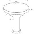
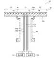
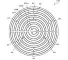
本発明の好適な実施形態を、図面を参照しながら以下に説明する。図1は第1実施形態のセラミックヒータ10の斜視図、図2はセラミックヒータ10の縦断面図(セラミックヒータ10を中心軸を含む面で切断したときの断面図)、図3はセラミックプレート20の抵抗発熱体22,24に沿って水平に切断して上方からみたときの断面図である。図3は、実質的にセラミックプレート20をウエハ載置面20aからみたときの様子を表している。なお、図3では、切断面を表すハッチングを省略した。 Preferred embodiments of the invention are described below with reference to the drawings. 1 is a perspective view of the
セラミックヒータ10は、エッチングやCVDなどの処理が施されるウエハを加熱するために用いられるものであり、図示しない真空チャンバ内に設置される。このセラミックヒータ10は、ウエハ載置面20aを有する円盤状のセラミックプレート20と、セラミックプレート20のウエハ載置面20aとは反対側の面(裏面)20bにセラミックプレート20と同軸となるように接合された筒状シャフト40とを備えている。 The
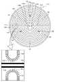
セラミックプレート20は、窒化アルミニウムやアルミナなどに代表されるセラミック材料からなる円盤状のプレートである。セラミックプレート20の直径は、例えば300mm程度である。セラミックプレート20のウエハ載置面20aには、図示しないが細かな凹凸がエンボス加工により設けられている。セラミックプレート20は、セラミックプレート20と同心円の仮想境界20c(図3参照)によって小円形の内周側ゾーンZ1と円環状の外周側ゾーンZ2とに分けられている。仮想境界20cの直径は、例えば200mm程度である。セラミックプレート20の内周側ゾーンZ1には内周側主抵抗発熱体22及び内周側副抵抗発熱体23が埋設され、外周側ゾーンZ2には外周側主抵抗発熱体24及び外周側副抵抗発熱体25が埋設されている。各抵抗発熱体22~25は、ウエハ載置面20aに平行な同一平面上に設けられている。 The
セラミックプレート20は、図3に示すように、複数のガス穴26を備えている。ガス穴26は、セラミックプレート20の裏面20bからウエハ載置面20aまで貫通しており、ウエハ載置面20aに設けられた凹凸とウエハ載置面20aに載置されるウエハWとの間に生じる隙間にガスを供給する。この隙間に供給されたガスは、ウエハ載置面20aとウエハWとの熱伝導を良好にする役割を果たす。また、セラミックプレート20は、複数のリフトピン穴28を備えている。リフトピン穴28は、セラミックプレート20の裏面20bからウエハ載置面20aまで貫通しており、図示しないリフトピンが挿通される。リフトピンは、ウエハ載置面20aに載置されたウエハWを持ち上げる役割を果たす。本実施形態では、リフトピン穴28は、同一円周上に等間隔となるように3つ設けられている。 The
内周側主抵抗発熱体22は、図3に示すように、セラミックプレート20の中央部(セラミックプレート20の裏面20bのうち筒状シャフト40で囲まれた領域)に配設された一対の主端子22a,22bの一方から端を発し、一筆書きの要領で複数の折り返し部で折り返されつつ内周側ゾーンZ1のほぼ全域に配線されたあと、一対の主端子22a,22bの他方に至るように形成されている。内周側主抵抗発熱体22は、リフトピン穴28を迂回するように設けられている。内周側主抵抗発熱体22は、高融点金属又はその炭化物を主成分とするコイルである。高融点金属としては、例えば、タングステン、モリブデン、タンタル、白金、レニウム、ハフニウム及びこれらの合金などが挙げられる。高融点金属の炭化物としては、例えば炭化タングステンや炭化モリブデンなどが挙げられる。内周側ゾーンZ1には、内周側主抵抗発熱体22のほかに、リフトピン穴28の周囲に内周側副抵抗発熱体23が設けられている(図3の左下枠参照)。リフトピン穴28の周囲には内周側主抵抗発熱体22のうちリフトピン穴28に接近している湾曲部22pがある。その湾曲部22pの外側に位置する内周側主抵抗発熱体22と湾曲部22pとで囲まれた網掛領域A1は、他の領域と比べて広いため、温度特異点になりやすい。そのため、その湾曲部22pを直線的に架け渡すようにリボン状(平らで細長い形状)の内周側副抵抗発熱体23が設けられている。架橋点間の内周側副抵抗発熱体23の電気抵抗は、特に限定するものではないが、例えば架橋点間の内周側主抵抗発熱体22(つまり湾曲部22p)の電気抵抗の10倍~100倍としてもよい。内周側副抵抗発熱体23の電気抵抗は、内周側副抵抗発熱体23の材料、断面積の大きさ、架橋点間の長さなどによって調整可能である。この内周側副抵抗発熱体23は、内周側主抵抗発熱体22と並列回路を構成している。内周側副抵抗発熱体23は、高融点金属又はその炭化物のペーストを印刷することにより形成することができる。なお、図3の左下枠には、1つのリフトピン穴28の周囲を拡大した図を示したが、他のリフトピン穴28の周囲も同様にして内周側副抵抗発熱体23が形成されている。また、湾曲部22pと内周側副抵抗発熱体23とを並列に設けることにより湾曲部22pの発熱量が低下することが問題となる場合は、湾曲部22pの発熱量が多くなるように、湾曲部22pのコイル巻きピッチを湾曲部22pの外側のコイル巻きピッチよりも小さくすることにより、改善することができる。As shown in FIG. 3, the inner peripheral side main
外周側主抵抗発熱体24は、図3に示すように、セラミックプレート20の中央部に配設された一対の端子24a,24bの一方から端を発し、一筆書きの要領で複数の折り返し部で折り返されつつ外周側ゾーンZ2のほぼ全域に配線されたあと一対の端子24a,24bの他方に至るように形成されている。外周側主抵抗発熱体24は、ガス穴26を迂回するように設けられている。外周側主抵抗発熱体24は、高融点金属又はその炭化物を主成分とするコイルである。但し、端子24a,24bから外周側ゾーンZ2に至るまでの区間は高融点金属又はその炭化物のワイヤ線で形成されている。外周側ゾーンZ2には、外周側主抵抗発熱体24のほかに、ガス穴26の周囲に外周側副抵抗発熱体25が設けられている(図3の右下枠参照)。ガス穴26の周囲には外周側主抵抗発熱体24のうちガス穴26を迂回している湾曲部24pがある。互いに向かい合う2つの湾曲部24pで囲まれた網掛領域A2は温度特異点になりやすい。そのため、その湾曲部24pを直線的に架け渡すようにリボン状の外周側副抵抗発熱体25が設けられている。架橋点間の外周側副抵抗発熱体25の電気抵抗は、特に限定するものではないが、例えば架橋点間の外周側主抵抗発熱体24(つまり湾曲部24p)の電気抵抗の10倍~100倍としてもよい。外周側副抵抗発熱体25の電気抵抗は、外周側副抵抗発熱体25の材料、断面積の大きさ、架橋点間の長さなどによって調整可能である。この外周側副抵抗発熱体25は、外周側主抵抗発熱体24と並列回路を構成している。外周側副抵抗発熱体25は、高融点金属又はその炭化物のペーストを印刷することにより形成することができる。なお、図3の右下枠には、1つのガス穴26の周囲を拡大した図を示したが、他のガス穴26の周囲も同様にして外周側副抵抗発熱体25が形成されている。また、湾曲部24pと外周側副抵抗発熱体25とを並列に設けることにより湾曲部24pの発熱量が低下することが問題となる場合は、湾曲部24pの発熱量が多くなるように、湾曲部24pのコイル巻きピッチを湾曲部24pの外側のコイル巻きピッチよりも小さくすることにより、改善することができる。As shown in FIG. 3, the outer peripheral main
筒状シャフト40は、セラミックプレート20と同じく窒化アルミニウム、アルミナなどのセラミックで形成されている。筒状シャフト40の内径は、例えば40mm程度、外径は例えば60mm程度である。この筒状シャフト40は、上端がセラミックプレート20に拡散接合されている。筒状シャフト40の内部には、内周側主抵抗発熱体22の一対の主端子22a,22bのそれぞれに接続される給電棒42a,42bや外周側主抵抗発熱体24の一対の端子24a,24bのそれぞれに接続される給電棒44a,44bが設けられている。給電棒42a,42bは第1電源32に接続され、給電棒44a,44bは第2電源34に接続されている。そのため、内周側主抵抗発熱体22及びこれに並列接続された内周側副抵抗発熱体23によって加熱される内周側ゾーンZ1と、外周側主抵抗発熱体24及びこれに並列接続された外周側副抵抗発熱体25によって加熱される外周側ゾーンZ2とを個別に温度制御することができる。なお、図示しないが、ガス穴26にガスを供給するガス供給管やリフトピン穴28に挿通されるリフトピンも筒状シャフト40の内部に配置される。 Like the
次に、セラミックヒータ10の使用例について説明する。まず、図示しない真空チャンバ内にセラミックヒータ10を設置し、そのセラミックヒータ10のウエハ載置面20aにウエハWを載置する。そして、図示しない内周側熱電対によって検出された内周側ゾーンZ1の温度が予め定められた内周側目標温度となるように、内周側主抵抗発熱体22及び内周側副抵抗発熱体23に供給する電力を第1電源32によって調整する。それと共に、図示しない外周側熱電対によって検出された外周側ゾーンZ2の温度が予め定められた外周側目標温度となるように、外周側主抵抗発熱体24及び外周側副抵抗発熱体25に供給する電力を第2電源34によって調整する。これにより、ウエハWの温度が所望の温度になるように制御される。そして、真空チャンバ内を真空雰囲気もしくは減圧雰囲気になるように設定し、真空チャンバ内にプラズマを発生させ、そのプラズマを利用してウエハWにCVD成膜を施したりエッチングを施したりする。 Next, a usage example of the
以上説明した本実施形態のセラミックヒータ10では、副抵抗発熱体23,25は、リボン状のため、印刷により作製することができ、線幅や線間を小さくすることができ、自由度の高い配線が可能になる。そのため、副抵抗発熱体23,25は、コイル状の主抵抗発熱体22,24による加熱を補完することができる。したがって、主抵抗発熱体22,24としてコイルを用いた場合でも十分な均熱性が得られる。 In the
また、主抵抗発熱体22,24はコイルのため配線するにあたっては制約がある。例えば、主抵抗発熱体22,24はガス穴26やリフトピン穴28を迂回して配線する必要がある。そのため、穴26,28の周囲は温度特異点になりやすい。ここでは、こうした穴26,28の周囲に副抵抗発熱体23,25が設けられているため、穴26,28の周囲が温度特異点になるのを防止することができる。 Also, since the main
更に、内周側副抵抗発熱体23は、内周側主抵抗発熱体22と並列回路を形成し、外周側副抵抗発熱体25は、外周側主抵抗発熱体24と並列回路を形成している。そのため、副抵抗発熱体23,25に専用の端子を設ける必要がない。 Further, the inner peripheral side secondary resistance heating element 23 forms a parallel circuit with the inner peripheral side main
なお、本発明は上述した実施形態に何ら限定されることはなく、本発明の技術的範囲に属する限り種々の態様で実施し得ることはいうまでもない。 It goes without saying that the present invention is not limited to the above-described embodiments, and can be implemented in various forms as long as they fall within the technical scope of the present invention.
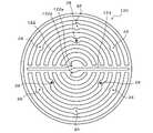
例えば、上述した実施形態のセラミックプレート20の代わりに、図4に示すセラミックプレート120を採用してもよい。図4はセラミックプレート120を抵抗発熱体122,123に沿って水平に切断して上方からみたときの断面図である(切断面を表すハッチングは省略した)。セラミックプレート120には、主抵抗発熱体122及び副抵抗発熱体123が埋設されている。主抵抗発熱体122は、一対の主端子122a,122bの一方から端を発し、一筆書きの要領で複数の折り返し部122cで折り返されつつウエハ載置面のほぼ全域に配線されたあと、一対の主端子122a,122bの他方に至るように形成されている。主抵抗発熱体122は、リフトピン穴28やガス穴26を迂回するように設けられている。主抵抗発熱体122は、高融点金属又はその炭化物を主成分とするコイルである。副抵抗発熱体123は、中央部に設けられた一対の副端子123a,123bの一方から端を発し、主抵抗発熱体122の折り返し部122c同士が向かい合っている部分を通過するように配線されたあと、一対の副端子123a,123bの他方に至るように形成されている。副抵抗発熱体123は、高融点金属又はその炭化物を主成分とするリボンであり、ペーストを印刷することにより形成されている。 For example, a
図4では、主抵抗発熱体122はコイルであるため、折り返し部122c同士が向かい合っている部分は比較的広くなっており温度特異点になりやすい。セラミックヒータ10を作製するにあたっては、コイルをセラミック粉末に埋設したあと焼成することがある。その場合、セラミック粉末内でコイルが移動することがあるため、それを考慮して折り返し部122c同士の距離を比較的広く設定する。ここでは、折り返し部122c同士が向かい合っている部分にはリボンである副抵抗発熱体123が印刷により設けられている。折り返し部122c同士の間隔は通常1mm程度必要である。これに対して、リボン同士の間隔はリボンが印刷で作製できることから0.3mm程度にすることができる。そのため、折り返し部122c同士が向かい合っている部分に副抵抗発熱体123を設けることができ、その部分が温度特異点になるのを防止することができる。また、主抵抗発熱体122の一対の主端子122a,122bを第1電源に接続し、副抵抗発熱体123の一対の副端子123a,123bを第1電源とは別の第2電源に接続すれば、主抵抗発熱体122による加熱と副抵抗発熱体123による加熱をそれぞれ独立して制御することができる。 In FIG. 4, since the main
なお、セラミックプレート120において、図5に示すように、副抵抗発熱体123を一対の主端子122a,122bの一方から他方に至るように形成してもよい。即ち、副抵抗発熱体123が主抵抗発熱体122と並列回路を形成するようにしてもよい。こうすれば、副抵抗発熱体123に専用の端子を設ける必要がない。 In addition, in the
図4及び図5において、上述した実施形態と同様に、リフトピン穴28の周囲やガス穴26の周囲に副抵抗発熱体23,25を設けてもよい。 4 and 5, auxiliary
上述した実施形態の副抵抗発熱体23,25や図4及び図5の副抵抗発熱体123や図6及び図7の副抵抗発熱体223は、セラミックを含有していてもよい。例えば、副抵抗発熱体23,25,123,223を印刷によって形成する際のペーストにセラミックを含有させてもよい。こうすることにより、副抵抗発熱体23,25,123,223の熱膨張係数をセラミックプレート20の熱膨張係数に近づけることができると共に副抵抗発熱体23,25,123,223とセラミックプレート20との接合強度を上げることができる。 The secondary
上述した実施形態のセラミックプレート20の代わりに、図6に示すセラミックプレート220を採用してもよい。図6はセラミックプレート220を抵抗発熱体222,223に沿って水平に切断して上方からみたときの断面図である(切断面を表すハッチングは省略した)。セラミックプレート220には、主抵抗発熱体222及び副抵抗発熱体223が埋設されている。主抵抗発熱体222は、一対の主端子222a,222bの一方から端を発し、一筆書きの要領で複数の折り返し部で折り返されつつウエハ載置面のほぼ全域に配線されたあと、一対の主端子222a,222bの他方に至るように形成されている。主抵抗発熱体222は、リフトピン穴28やガス穴26を迂回するように設けられている。主抵抗発熱体222は、高融点金属又はその炭化物を主成分とするコイルである。副抵抗発熱体223は、一対の副端子223a,223bの一方から端を発し、主抵抗発熱体222に沿って配線されたあと、一対の副端子223a,223bの他方に至るように形成されている。副抵抗発熱体223は、高融点金属又はその炭化物を主成分とするリボンであり、ペーストを印刷することにより形成されている。 A
図6では、主抵抗発熱体222はコイルであるため、コイル同士の間隔は比較的広くなっており温度特異点になりやすい。ここでは、コイル同士の間隔にはリボンである副抵抗発熱体223が印刷により設けられている。コイル同士の間隔は通常1mm程度必要である。これに対して、リボン同士の間隔はリボンが印刷で作製できることから0.3mm程度にすることができる。そのため、コイル同士の間隔に副抵抗発熱体223を設けることができ、その部分が温度特異点になるのを防止することができる。また、主抵抗発熱体222の一対の主端子222a,222bを第1電源に接続し、副抵抗発熱体223の一対の副端子223a,223bを第1電源とは別の第2電源に接続すれば、主抵抗発熱体222による加熱と副抵抗発熱体223による加熱をそれぞれ独立して制御することができる。 In FIG. 6, since the main
なお、セラミックプレート220において、図7に示すように、副抵抗発熱体223を一対の主端子222a,222bの一方から他方に至るように形成してもよい。即ち、副抵抗発熱体223が主抵抗発熱体222と並列回路を形成するようにしてもよい。こうすれば、副抵抗発熱体223に専用の端子を設ける必要がなくなる。 In addition, in the
上述した実施形態では、副抵抗発熱体23,25をリボンとしたが、特にこれに限定されるものではなく、二次元形状であればどのような形状を採用してもよい。二次元形状であれば、ペーストを印刷することにより作製できるため、副抵抗発熱体23,25を容易に細くすることができ、高密度に配線することができる。 In the above-described embodiment, the auxiliary
上述した実施形態において、セラミックプレート20に静電電極を内蔵してもよい。その場合、ウエハ載置面20aにウエハWを載置したあと静電電極に電圧を印加することによりウエハWをウエハ載置面20aに静電吸着することができる。あるいは、セラミックプレート20にRF電極を内蔵してもよい。その場合、ウエハ載置面20aの上方にスペースをあけて図示しないシャワーヘッドを配置し、シャワーヘッドとRF電極とからなる平行平板電極間に高周波電力を供給する。こうすることによりプラズマを発生させ、そのプラズマを利用してウエハWにCVD成膜を施したりエッチングを施したりすることができる。なお、静電電極をRF電極と兼用してもよい。この点は、図4~図7のセラミックプレート120,220についても同様である。 In the above-described embodiments, the
上述した実施形態では、外周側ゾーンZ2は1つのゾーンとして説明したが、複数の小ゾーンに分割されていてもよい。その場合、抵抗発熱体は小ゾーンごとに独立して配線される。小ゾーンは、セラミックプレート20と同心円の境界線で外周側ゾーンZ2を分割することにより環状に形成してもよいし、セラミックプレート20の中心から放射状に延びる線分で外周側ゾーンZ2を分割することにより扇形(円錐台の側面を展開した形状)に形成してもよい。 In the embodiment described above, the outer zone Z2 was explained as one zone, but it may be divided into a plurality of small zones. In that case, the resistance heating elements are wired independently for each small zone. The small zones may be formed in an annular shape by dividing the outer zone Z2 by a boundary line concentric with the
上述した実施形態では、内周側ゾーンZ1は1つのゾーンとして説明したが、複数の小ゾーンに分割されていてもよい。その場合、抵抗発熱体は小ゾーンごとに独立して配線される。小ゾーンは、セラミックプレート20と同心円の境界線で内周側ゾーンZ1を分割することにより環状と円形状に形成してもよいし、セラミックプレート20の中心から放射状に延びる線分で内周側ゾーンZ1を分割することにより扇形(円錐の側面を展開した形状)に形成してもよい。 In the embodiment described above, the inner peripheral zone Z1 was explained as one zone, but it may be divided into a plurality of small zones. In that case, the resistance heating elements are wired independently for each small zone. The small zones may be formed in annular and circular shapes by dividing the inner peripheral zone Z1 at a boundary line that is concentric with the
本出願は、2019年1月25日に出願された日本国特許出願第2019-011300号を優先権主張の基礎としており、引用によりその内容の全てが本明細書に含まれる。 This application claims priority from Japanese Patent Application No. 2019-011300 filed on January 25, 2019, the entire contents of which are incorporated herein by reference.
本発明は、半導体製造装置に利用可能である。 INDUSTRIAL APPLICABILITY The present invention is applicable to semiconductor manufacturing equipment.
10 セラミックヒータ、20 セラミックプレート、20a ウエハ載置面、20b 裏面、20c 仮想境界、22 内周側主抵抗発熱体、22a,22b 主端子、22p 湾曲部、23 内周側副抵抗発熱体、24 外周側主抵抗発熱体、24a,24b 端子、24p 湾曲部、25 外周側副抵抗発熱体、26 ガス穴、28 リフトピン穴、32 第1電源、34 第2電源、40 筒状シャフト、42a,42b 給電棒、44a,44b 給電棒、120 セラミックプレート、122 主抵抗発熱体、122a,122b 主端子、122c 折り返し部、123 副抵抗発熱体、123a,123b 副端子、220 セラミックプレート、222 主抵抗発熱体、222a,222b 主端子、223 副抵抗発熱体、223a,223b 副端子、W ウエハ、Z1 内周側ゾーン、Z2 外周側ゾーン。
Claims (7)
Translated fromJapanese前記セラミックプレートの内部に前記ウエハ載置面と平行に設けられ、一対の主端子の一方から一筆書きの要領で配線されたあと前記一対の主端子の他方に至るコイル状の主抵抗発熱体と、
前記セラミックプレートの内部に設けられ、前記主抵抗発熱体による加熱を補完する二次元形状の副抵抗発熱体と、
を備え、
前記主抵抗発熱体は、前記一対の主端子の一方から複数の折り返し部で折り返されつつ前記一対の主端子の他方に至るように形成されており、
前記副抵抗発熱体は、前記主抵抗発熱体の前記折り返し部同士が向かい合っている部分に設けられている、
セラミックヒータ。a ceramic plate having a wafer mounting surface;
a coil-shaped main resistance heating element provided inside the ceramic plate in parallel with the wafer mounting surface, and connected to the other of the pair of main terminals after being wired in a unicursal manner from one of the pair of main terminals; ,
a two-dimensional auxiliary resistance heating element provided inside the ceramic plate and complementing heating by the main resistance heating element;
with
The main resistance heating element is formed to extend from one of the pair of main terminals to the other of the pair of main terminals while being folded back at a plurality of folded portions,
The secondary resistance heating element is provided at a portion where the folded portions of the main resistance heating element face each other,
ceramic heater.
前記セラミックプレートの内部に前記ウエハ載置面と平行に設けられ、一対の主端子の一方から一筆書きの要領で配線されたあと前記一対の主端子の他方に至るコイル状の主抵抗発熱体と、
前記セラミックプレートの内部に設けられ、前記主抵抗発熱体による加熱を補完する二次元形状の副抵抗発熱体と、
を備え、
前記副抵抗発熱体は、前記主抵抗発熱体と並列回路を形成している、
セラミックヒータ。a ceramic plate having a wafer mounting surface;
a coil-shaped main resistance heating element provided inside the ceramic plate in parallel with the wafer mounting surface, and connected to the other of the pair of main terminals after being wired in a unicursal manner from one of the pair of main terminals; ,
a two-dimensional auxiliary resistance heating element provided inside the ceramic plate and complementing heating by the main resistance heating element;
with
The auxiliary resistance heating element forms a parallel circuit with the main resistance heating element,
ceramic heater.
請求項1又は2に記載のセラミックヒータ。The auxiliary resistance heating element is provided at intervals between the wirings of the main resistance heating element,
The ceramic heater according to claim 1or 2 .
請求項1~3に記載のセラミックヒータ。The sub-resistance heating element is wired from one of the pair of sub-terminals to the other of the pair of sub-terminals after being wired in a unicursal manner,
A ceramic heater according to any one of claims 1 to3 .
請求項1~4のいずれか1項に記載のセラミックヒータ。The secondary resistance heating element contains ceramic,
The ceramic heater according to any one of claims1-4 .
前記セラミックプレートの内部に前記ウエハ載置面と平行に設けられ、一対の主端子の一方から一筆書きの要領で配線されたあと前記一対の主端子の他方に至るコイル状の主抵抗発熱体と、
前記セラミックプレートの内部に設けられ、前記主抵抗発熱体による加熱を補完する二次元形状の副抵抗発熱体と、
を備え、
前記副抵抗発熱体は、前記主抵抗発熱体の湾曲部を架橋するように設けられ、
前記湾曲部のコイル巻きピッチは、前記湾曲部の外側のコイル巻きピッチよりも小さい、
セラミックヒータ。a ceramic plate having a wafer mounting surface;
a coil-shaped main resistance heating element provided inside the ceramic plate in parallel with the wafer mounting surface, and connected to the other of the pair of main terminals after being wired in a unicursal manner from one of the pair of main terminals; ,
a two-dimensional auxiliary resistance heating element provided inside the ceramic plate and complementing heating by the main resistance heating element;
with
The auxiliary resistance heating element is provided so as to bridge the curved portion of the main resistance heating element,
the coil winding pitch of the curved portion is smaller than the coil winding pitch outside the curved portion;
ceramic heater.
前記副抵抗発熱体は、前記穴の周囲に設けられている、 The auxiliary resistance heating element is provided around the hole,
請求項1~6のいずれか1項に記載のセラミックヒータ。 The ceramic heater according to any one of claims 1-6.
Applications Claiming Priority (3)
| Application Number | Priority Date | Filing Date | Title |
|---|---|---|---|
| JP2019011300 | 2019-01-25 | ||
| JP2019011300 | 2019-01-25 | ||
| PCT/JP2019/050764WO2020153086A1 (en) | 2019-01-25 | 2019-12-25 | Ceramic heater |
Publications (2)
| Publication Number | Publication Date |
|---|---|
| JPWO2020153086A1 JPWO2020153086A1 (en) | 2021-09-30 |
| JP7123181B2true JP7123181B2 (en) | 2022-08-22 |
Family
ID=71736808
Family Applications (1)
| Application Number | Title | Priority Date | Filing Date |
|---|---|---|---|
| JP2020568036AActiveJP7123181B2 (en) | 2019-01-25 | 2019-12-25 | ceramic heater |
Country Status (6)
| Country | Link |
|---|---|
| US (1) | US20210235548A1 (en) |
| JP (1) | JP7123181B2 (en) |
| KR (1) | KR102514749B1 (en) |
| CN (1) | CN113056961B (en) |
| TW (1) | TWI837264B (en) |
| WO (1) | WO2020153086A1 (en) |
Families Citing this family (3)
| Publication number | Priority date | Publication date | Assignee | Title |
|---|---|---|---|---|
| KR102639158B1 (en)* | 2019-07-23 | 2024-02-22 | 삼성전자주식회사 | Wafer processing apparatus, and wafer processing method using the same |
| CN120642044A (en) | 2023-02-10 | 2025-09-12 | 日本碍子株式会社 | Multi-zone heater |
| KR102762457B1 (en)* | 2024-04-22 | 2025-02-04 | 주식회사 미코세라믹스 | Ceramic heater |
Citations (5)
| Publication number | Priority date | Publication date | Assignee | Title |
|---|---|---|---|---|
| JP2003272805A (en) | 2002-03-18 | 2003-09-26 | Ngk Insulators Ltd | Ceramic heater |
| JP2005026120A (en) | 2003-07-03 | 2005-01-27 | Ibiden Co Ltd | Ceramic heater |
| JP2005063691A (en) | 2003-08-13 | 2005-03-10 | Ngk Insulators Ltd | Heating apparatus |
| JP2008270198A (en) | 2007-03-26 | 2008-11-06 | Ngk Insulators Ltd | Heating device |
| JP3182120U (en) | 2012-12-26 | 2013-03-07 | 日本碍子株式会社 | Ceramic heater |
Family Cites Families (10)
| Publication number | Priority date | Publication date | Assignee | Title |
|---|---|---|---|---|
| JP4040814B2 (en)* | 1998-11-30 | 2008-01-30 | 株式会社小松製作所 | Disk heater and temperature control device |
| JP3897563B2 (en)* | 2001-10-24 | 2007-03-28 | 日本碍子株式会社 | Heating device |
| WO2006004045A1 (en)* | 2004-07-05 | 2006-01-12 | Tokyo Electron Limited | Treating device and heater unit |
| EP2048914B1 (en)* | 2007-10-10 | 2013-10-02 | LG Electronics Inc. | A cooking device having an induction heating element |
| TWI527500B (en)* | 2010-05-13 | 2016-03-21 | 應用材料股份有限公司 | Heater with independent center zone control |
| JP6424010B2 (en)* | 2014-03-31 | 2018-11-14 | 株式会社美鈴工業 | Heater, fixing device including the same, image forming apparatus, heating device, and heater manufacturing method |
| JP6202111B2 (en)* | 2014-11-20 | 2017-09-27 | 住友大阪セメント株式会社 | Electrostatic chuck device |
| JP6804828B2 (en)* | 2015-04-20 | 2020-12-23 | 日本特殊陶業株式会社 | Ceramic heater and electrostatic chuck |
| JP6622052B2 (en)* | 2015-10-14 | 2019-12-18 | 日本特殊陶業株式会社 | Ceramic heater and electrostatic chuck |
| KR102373639B1 (en)* | 2017-10-27 | 2022-03-14 | 교세라 가부시키가이샤 | Heaters and Heater Systems |
- 2019
- 2019-12-25WOPCT/JP2019/050764patent/WO2020153086A1/ennot_activeCeased
- 2019-12-25JPJP2020568036Apatent/JP7123181B2/enactiveActive
- 2019-12-25CNCN201980076037.3Apatent/CN113056961B/enactiveActive
- 2019-12-25KRKR1020217013830Apatent/KR102514749B1/enactiveActive
- 2019-12-26TWTW108147803Apatent/TWI837264B/enactive
- 2021
- 2021-04-14USUS17/301,773patent/US20210235548A1/enactivePending
Patent Citations (5)
| Publication number | Priority date | Publication date | Assignee | Title |
|---|---|---|---|---|
| JP2003272805A (en) | 2002-03-18 | 2003-09-26 | Ngk Insulators Ltd | Ceramic heater |
| JP2005026120A (en) | 2003-07-03 | 2005-01-27 | Ibiden Co Ltd | Ceramic heater |
| JP2005063691A (en) | 2003-08-13 | 2005-03-10 | Ngk Insulators Ltd | Heating apparatus |
| JP2008270198A (en) | 2007-03-26 | 2008-11-06 | Ngk Insulators Ltd | Heating device |
| JP3182120U (en) | 2012-12-26 | 2013-03-07 | 日本碍子株式会社 | Ceramic heater |
Also Published As
| Publication number | Publication date |
|---|---|
| US20210235548A1 (en) | 2021-07-29 |
| CN113056961A (en) | 2021-06-29 |
| JPWO2020153086A1 (en) | 2021-09-30 |
| WO2020153086A1 (en) | 2020-07-30 |
| CN113056961B (en) | 2023-06-02 |
| TW202033052A (en) | 2020-09-01 |
| KR102514749B1 (en) | 2023-03-27 |
| TWI837264B (en) | 2024-04-01 |
| KR20210068128A (en) | 2021-06-08 |
Similar Documents
| Publication | Publication Date | Title |
|---|---|---|
| JP7216746B2 (en) | ceramic heater | |
| US11956863B2 (en) | Multi-zone heater | |
| JP7212070B2 (en) | ceramic heater | |
| JP7123181B2 (en) | ceramic heater | |
| KR101427427B1 (en) | Heating device | |
| JP6715699B2 (en) | Ceramics heater | |
| KR102581101B1 (en) | Ceramic heater and its manufacturing method | |
| US10679873B2 (en) | Ceramic heater | |
| JP7321990B2 (en) | ceramic heater | |
| JP7727114B1 (en) | Ceramic heater | |
| JP2005063691A (en) | Heating apparatus |
Legal Events
| Date | Code | Title | Description |
|---|---|---|---|
| A621 | Written request for application examination | Free format text:JAPANESE INTERMEDIATE CODE: A621 Effective date:20210412 | |
| A131 | Notification of reasons for refusal | Free format text:JAPANESE INTERMEDIATE CODE: A131 Effective date:20220524 | |
| A521 | Request for written amendment filed | Free format text:JAPANESE INTERMEDIATE CODE: A523 Effective date:20220705 | |
| TRDD | Decision of grant or rejection written | ||
| A01 | Written decision to grant a patent or to grant a registration (utility model) | Free format text:JAPANESE INTERMEDIATE CODE: A01 Effective date:20220726 | |
| A61 | First payment of annual fees (during grant procedure) | Free format text:JAPANESE INTERMEDIATE CODE: A61 Effective date:20220809 | |
| R150 | Certificate of patent or registration of utility model | Ref document number:7123181 Country of ref document:JP Free format text:JAPANESE INTERMEDIATE CODE: R150 |