JP7121403B2 - RF tag device - Google Patents
RF tag deviceDownload PDFInfo
- Publication number
- JP7121403B2 JP7121403B2JP2019535695AJP2019535695AJP7121403B2JP 7121403 B2JP7121403 B2JP 7121403B2JP 2019535695 AJP2019535695 AJP 2019535695AJP 2019535695 AJP2019535695 AJP 2019535695AJP 7121403 B2JP7121403 B2JP 7121403B2
- Authority
- JP
- Japan
- Prior art keywords
- waveguide element
- tag
- metal material
- antenna
- pressure pipe
- Prior art date
- Legal status (The legal status is an assumption and is not a legal conclusion. Google has not performed a legal analysis and makes no representation as to the accuracy of the status listed.)
- Active
Links
Images


Classifications
- G—PHYSICS
- G06—COMPUTING OR CALCULATING; COUNTING
- G06K—GRAPHICAL DATA READING; PRESENTATION OF DATA; RECORD CARRIERS; HANDLING RECORD CARRIERS
- G06K19/00—Record carriers for use with machines and with at least a part designed to carry digital markings
- G06K19/06—Record carriers for use with machines and with at least a part designed to carry digital markings characterised by the kind of the digital marking, e.g. shape, nature, code
- G06K19/067—Record carriers with conductive marks, printed circuits or semiconductor circuit elements, e.g. credit or identity cards also with resonating or responding marks without active components
- G06K19/07—Record carriers with conductive marks, printed circuits or semiconductor circuit elements, e.g. credit or identity cards also with resonating or responding marks without active components with integrated circuit chips
- G06K19/077—Constructional details, e.g. mounting of circuits in the carrier
- H—ELECTRICITY
- H01—ELECTRIC ELEMENTS
- H01Q—ANTENNAS, i.e. RADIO AERIALS
- H01Q1/00—Details of, or arrangements associated with, antennas
- H01Q1/12—Supports; Mounting means
- H01Q1/22—Supports; Mounting means by structural association with other equipment or articles
- H—ELECTRICITY
- H01—ELECTRIC ELEMENTS
- H01Q—ANTENNAS, i.e. RADIO AERIALS
- H01Q1/00—Details of, or arrangements associated with, antennas
- H01Q1/36—Structural form of radiating elements, e.g. cone, spiral, umbrella; Particular materials used therewith
- H01Q1/38—Structural form of radiating elements, e.g. cone, spiral, umbrella; Particular materials used therewith formed by a conductive layer on an insulating support
- H—ELECTRICITY
- H01—ELECTRIC ELEMENTS
- H01Q—ANTENNAS, i.e. RADIO AERIALS
- H01Q13/00—Waveguide horns or mouths; Slot antennas; Leaky-waveguide antennas; Equivalent structures causing radiation along the transmission path of a guided wave
- H01Q13/08—Radiating ends of two-conductor microwave transmission lines, e.g. of coaxial lines, of microstrip lines
Landscapes
- Engineering & Computer Science (AREA)
- Computer Hardware Design (AREA)
- Microelectronics & Electronic Packaging (AREA)
- Physics & Mathematics (AREA)
- General Physics & Mathematics (AREA)
- Theoretical Computer Science (AREA)
- Support Of Aerials (AREA)
- Details Of Rigid Or Semi-Rigid Containers (AREA)
Description
Translated fromJapanese本発明は、高圧配管など管形状を有する金属資材の在庫管理、物流管理などをRFタグで管理するためのRFタグ装置に関する。特に、本発明は管形状を有する金属資材にRFタグを取り付けた場合でも、通信距離が長くまた開口面積が広くなり読取装置によって効果的に読み取ることができるRFタグ装置に関する。 TECHNICAL FIELD The present invention relates to an RF tag device for managing inventory management, physical distribution management, etc. of tubular metal materials such as high-pressure pipes. More particularly, the present invention relates to an RF tag device that can be effectively read by a reading device even when the RF tag is attached to a metal material having a tubular shape, because the communication distance is long and the opening area is widened.
近年、製品や部品等の在庫管理、物流管理等を行う管理システムにおいて、RFID(Radio Frequency Identification)技術が利用されている。このRFID技術を用いたシステムでは、RFタグとリーダライタ(以下、読取装置という。)との間で無線通信が行われ、RFタグに記憶される識別情報等が読取装置により読み取られる。
例えば、特許文献1(WO2007/000807号公報)には、薄くてフレキシブルで金属に貼り付けても通信でき、製造コストも低減する無線周波数識別タグについて開示されている。In recent years, RFID (Radio Frequency Identification) technology has been used in management systems for inventory management, physical distribution management, and the like of products and parts. In a system using this RFID technology, wireless communication is performed between an RF tag and a reader/writer (hereinafter referred to as a reader), and identification information and the like stored in the RF tag are read by the reader.
For example, Patent Literature 1 (WO2007/000807) discloses a radio frequency identification tag that is thin and flexible, can communicate even when attached to metal, and has a reduced manufacturing cost.
特許文献1に記載の無線周波数識別タグにおいては、逆Fアンテナ(10)は、放射エレメント(11)、ショートピン(12)、給電部(13)、およびグランド地板(14)を有し、フィルム(30)の表面に平面状に形成されている。フィルム(30)は、例えば、ポリエチレンテレフタレートなどの絶縁フィルムであり、表面に形成された逆Fアンテナ(10)の放射エレメント(11)、ショートピン(12)、および給電部(13)が、電子機器などの金属筐体(40)から突出するように貼り付けられるものである。 In the radio frequency identification tag described in Patent Document 1, an inverted F antenna (10) has a radiating element (11), a short pin (12), a feeder (13) and a ground plane (14), and a film It is formed flat on the surface of (30). The film (30) is, for example, an insulating film such as polyethylene terephthalate. It is attached so as to protrude from a metal housing (40) of equipment or the like.
特許文献2(特開2003-85501号公報)には、金属などの導電体に貼付しても、外部機器(リーダライタ)と交信可能な非接触ICタグについて開示されている。 Patent Document 2 (Japanese Unexamined Patent Application Publication No. 2003-85501) discloses a contactless IC tag that can communicate with an external device (reader/writer) even when attached to a conductor such as metal.
特許文献2に記載の非接触ICタグにおいては、静電結合方式によって、2つのアンテナ間に電位差を生じさせて、外部機器と非接触で交信可能な非接触ICタグであって、導電体40に貼付可能であって、その導電体40との導通を防止する絶縁層11と、絶縁層11に形成された導電層12と、ICチップ13Dを実装し、一部分を導電層12に形成し、他の部分を導電体40に貼付するICチップ実装部13とを備え、導電層12を第1のアンテナとし、導電体40を第2のアンテナにするものである。 The non-contact IC tag described in Patent Document 2 is a non-contact IC tag capable of non-contact communication with an external device by generating a potential difference between two antennas by an electrostatic coupling method. mounting an insulating layer 11 that can be attached to and prevents conduction with the
特許文献3(WO2009/069199号公報)には、RFタグにより管理される金属パイプに関し、長手方向に所定の長さを持つスロットが空けられ、内側に、スロットに給電する給電部とこの給電部に接続されるICチップとを有するRFタグが取り付けられることによりRFタグのアンテナとして機能するように構成することにより、この金属パイプがRFタグにより管理されるものについて開示されている。 Patent Document 3 (WO2009/069199) relates to a metal pipe managed by an RF tag. The metal pipe is managed by the RF tag by attaching the RF tag having an IC chip connected to the metal pipe so that it functions as an antenna of the RF tag.
特許文献3に記載のRFタグは、長手方向に所定の長さを持つスロットが空けられた金属パイプの内側に設けられ、前記金属パイプをアンテナとして機能させるために前記スロットに給電する給電部と、前記金属パイプの内側に設けられ前記給電部に接続されるIC(Integrated Circuit)チップと、を備えるものである。 The RF tag described in Patent Document 3 is provided inside a metal pipe having a slot having a predetermined length in the longitudinal direction, and a power feeding part that feeds power to the slot in order to make the metal pipe function as an antenna. and an IC (Integrated Circuit) chip provided inside the metal pipe and connected to the power feeder.
しかし、特許文献1に開示された無線周波数識別タグでは、逆Fアンテナ(10)の放射エレメント(11)、ショートピン(12)、および給電部(13)が金属筐体(40)から突出するように貼り付ける必要があるので、金属筐体から突出した部分が邪魔になるため高圧配管などの管形状を有する金属資材に取り付けることはできない。 However, in the radio frequency identification tag disclosed in US Pat. Therefore, it cannot be attached to tubular metal materials such as high-pressure pipes because the portion protruding from the metal housing becomes an obstacle.
特許文献2に開示された非接触ICタグでは、静電結合方式によって2つのアンテナ間に電位差を生じさせているので、通信距離が非常に短いという欠点がある。
特許文献3に開示された発明では、金属パイプにスロットを設ける必要があるので、スロットを設けることができない金属資材に適用することはできない。The non-contact IC tag disclosed in Patent Document 2 has the disadvantage that the communication distance is very short because a potential difference is generated between the two antennas by the electrostatic coupling method.
The invention disclosed in Patent Document 3 cannot be applied to metal materials that cannot be provided with slots because it is necessary to provide slots in the metal pipe.
本発明の主な目的は、高圧配管などの管形状を有する金属資材にRFタグを取り付けた場合でも、通信距離が長くまた開口面積が広くなり読取装置によって効果的に読み取ることができるRFタグ装置を提供することである。
本発明の他の目的は、複数の金属資材を束ね、または複数の金属資材を積み重ねるような場合でも、複数の金属資材に固定されたRFタグを同時に読み取ることができるRFタグ装置を提供することである。The main object of the present invention is to provide an RF tag device that can be effectively read by a reader with a long communication distance and a wide opening area even when the RF tag is attached to a metal material having a tubular shape such as a high-pressure pipe. is to provide
Another object of the present invention is to provide an RF tag device capable of simultaneously reading RF tags fixed to a plurality of metal materials even when a plurality of metal materials are bundled or stacked. is.
(1)
一局面に従うRFタグ装置は、管形状を有する金属資材に取り付けられるRFタグ装置であって、RFタグ装置は、固定治具と、RFタグと、を含み、固定治具は、管形状を有する金属資材の開口端部に取り付けられる平板部と、平板部の裏面から管形状を有する金属資材内へ延設されるとともに管形状を有する金属資材の内周面に係止する1または複数の係止片と、を有し、平板部の表面にRFタグを固定するものである。(1)
An RF tag device according to one aspect is an RF tag device attached to a metal material having a tubular shape, the RF tag device including a fixture and an RF tag, the fixture having a tubular shape. A flat plate portion attached to the open end of the metal material, and one or more hooks extending from the back surface of the flat plate portion into the metal material having a tubular shape and engaging with the inner peripheral surface of the metal material having a tubular shape. and a stop piece for fixing the RF tag to the surface of the flat plate portion.
この場合、固定治具の平板部の固定部にRFタグを固定し、この固定治具の係止片を金属資材の内周面に係止させるようにして固定治具を金属資材に取り付ける。ここで、固定治具の平板部にRFタグを電気絶縁性の貼着部材により貼着することで、コンデンサが形成され、RFタグのインダクタンスと共振回路を形成することができる。 In this case, the fixing jig is attached to the metal material by fixing the RF tag to the fixing portion of the flat plate portion of the fixing jig and engaging the locking piece of the fixing jig with the inner peripheral surface of the metal material. Here, by attaching the RF tag to the flat plate portion of the fixing jig with an electrically insulating attaching member, a capacitor is formed, and an inductance of the RF tag and a resonance circuit can be formed.
一般的に金属資材の直径が、16cm以下の場合、RFタグを金属資材内に収容した場合、読取装置の電波をRFタグが受信できないという問題が生じる。
しかしながら、本発明においては、金属資材の外部にRFタグを固定させつつ、露出させることができるので、読取装置の電波を確実に受信することができる。In general, if the metal material has a diameter of 16 cm or less and the RF tag is housed in the metal material, there arises a problem that the RF tag cannot receive radio waves from the reader.
However, in the present invention, since the RF tag can be exposed while being fixed to the outside of the metal material, radio waves from the reader can be reliably received.
すなわち、読取装置からの電波は、RFタグの一方の導波素子(第1導波素子)により受信され、RFタグの第1導波素子と、該RFタグの他方の第2導波素子(グランドエレメント)との間に接続されたICチップ回路を通し、第2導波素子より固定治具を介して金属パイプに放出される。つまり、RFタグと固定治具が貼着部材からなる誘電体を介して容量結合をするため、固定治具がアンテナとして機能する。 That is, the radio waves from the reader are received by one waveguide element (first waveguide element) of the RF tag, and the first waveguide element of the RF tag and the other second waveguide element of the RF tag ( ground element), and emitted from the second waveguide element to a metal pipe via a fixture. That is, since the RF tag and the fixing jig are capacitively coupled through the dielectric made of the sticking member, the fixing jig functions as an antenna.
よって、金属資材全体がアンテナとなり作動することができる。このようにして、RFタグからの電波を、金属資材を介して読取装置へ送ることができ、かつ読取装置からの電波を、金属資材を介してRFタグで受信することができる。
その結果、RFタグを確実に駆動させ、無指向性で通信距離が長いRFタグの読み取りを実施することができる。Therefore, the entire metal material can act as an antenna. In this way, radio waves from the RF tag can be sent to the reader through the metal material, and radio waves from the reader can be received by the RF tag through the metal material.
As a result, it is possible to reliably drive the RF tag and read the non-directional RF tag with a long communication distance.
したがって、複数のパイプなどの金属パイプが束ねられ、あるいは積み重ねられて保管されている場合に、RFタグが金属パイプに隠れて電波を受信できないような場合でも、各金属パイプに取り付けられたRFタグの履歴情報などを同時に読み取ることができる。 Therefore, when metal pipes such as a plurality of pipes are bundled or stacked and stored, even if the RF tag is hidden by the metal pipes and cannot receive radio waves, the RF tag attached to each metal pipe history information, etc. can be read at the same time.
(2)
第2の発明にかかるRFタグ装置は、一局面に従うRFタグ装置において、RFタグは、アンテナと、読取装置から送信された電波に基づいて動作するICチップと、を含み、アンテナは、絶縁層を介して設けられた第1導波素子及び第2導波素子と、第2導波素子に一端が電気的に接続された給電部と、第1導波素子に一端が電気的に接続され、第2導波素子に他端が電気的に接続された短絡部と、を含み、絶縁層、第1導波素子、第2導波素子、給電部及び短絡部により、読取装置から送信された電波を受信するように構成され、第1導波素子、短絡部、第2導波素子及び給電部により構成されるインダクタパターンと、第1導波素子、第2導波素子及び絶縁層により構成されるコンデンサとにより、電波の周波数帯域で共振する共振回路が構成されるものでもよい。(2)
An RF tag device according to a second aspect of the invention is an RF tag device according to one aspect, wherein the RF tag includes an antenna and an IC chip that operates based on radio waves transmitted from a reader, and the antenna includes an insulating layer A first waveguide element and a second waveguide element provided via, a feeding section having one end electrically connected to the second waveguide element, and one end electrically connected to the first waveguide element , and a short-circuit portion having the other end electrically connected to the second waveguide element, wherein the signal is transmitted from the reader by the insulating layer, the first waveguide element, the second waveguide element, the feeding portion, and the short-circuit portion. a first waveguide element, a short-circuiting portion, a second waveguide element, and an inductor pattern configured to receive radio waves; A resonant circuit that resonates in the frequency band of radio waves may be configured with the configured capacitor.
この場合、RFタグは、アンテナ及びICチップを備えている。RFタグは、読取装置のアンテナから送信された電波(搬送波)をRFタグの導波素子(アンテナ)で受信する。そして、ICチップに記録されている金属資材の識別データ等を反射波に乗せて読取装置へ返送する。これにより、読取装置をRFタグに接触させることなく、RFタグは読取装置と通信することが可能である。 In this case, the RF tag has an antenna and an IC chip. The RF tag receives a radio wave (carrier wave) transmitted from the antenna of the reader with a waveguide element (antenna) of the RF tag. Then, identification data of the metal material recorded in the IC chip is put on the reflected wave and sent back to the reading device. This allows the RF tag to communicate with the reader without bringing the reader into contact with the RF tag.
(3)
第3の発明にかかるRFタグ装置は、一局面または第2の発明にかかるRFタグ装置において、1または複数の係止片は、管形状を有する金属資材の内周面に対して付勢する付勢部材からなるものでもよい。(3)
An RF tag device according to a third aspect of the invention is the RF tag device according to one aspect or the second aspect of the invention, wherein the one or more locking pieces bias against the inner peripheral surface of the metal material having a tubular shape. It may consist of an urging member.
この場合、固定治具を金属資材に取り付けるときは、係止片を弾性変形させることで固定治具を金属資材に容易に取り付けることができ、また固定治具を金属資材に取り付けた後では係止片が金属資材の内周面に付勢により押圧するので固定治具を金属資材に確実に取り付けることができる。 In this case, when the fixing jig is attached to the metal material, the fixing jig can be easily attached to the metal material by elastically deforming the locking piece. Since the stop piece presses against the inner peripheral surface of the metal material, the fixing jig can be securely attached to the metal material.
(4)
第4の発明にかかるRFタグ装置は、一局面から第3の発明にかかるRFタグ装置において、金属資材が高圧配管であってもよい。(4)
An RF tag device according to a fourth aspect of the present invention is the RF tag device according to the first aspect to the third aspect of the invention, wherein the metal material may be a high-pressure pipe.
この場合、読取装置は、高圧配管に取り付けられたRFタグから資材情報を読み取るため、高圧配管の移動、保管などの管理を行うことができる。 In this case, since the reading device reads the material information from the RF tag attached to the high-pressure pipe, it is possible to manage the movement and storage of the high-pressure pipe.
以下、図面を参照しつつ、本発明の実施の形態について説明する。以下の説明では、同一の部品には同一の符号を付す。また、同符号の場合には、それらの名称および機能も同一である。したがって、それらについての詳細な説明は繰り返さないものとする。 BEST MODE FOR CARRYING OUT THE INVENTION Hereinafter, embodiments of the present invention will be described with reference to the drawings. In the following description, the same reference numerals are given to the same parts. Moreover, in the case of the same reference numerals, their names and functions are also the same. Therefore, detailed description thereof will not be repeated.
[本実施の形態]
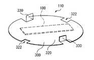
図1は、本実施の形態にかかるRFタグ装置110を高圧配管200の開口端部210に取り付けた状態の一例を示す模式的断面図であり、図2および図3は、本実施の形態にかかるRFタグ装置110の一例を示す模式的斜視図である。[Embodiment]
FIG. 1 is a schematic cross-sectional view showing an example of a state in which an
本発明のRFタグ装置110は管形状を有する金属資材200の開口端部210に取り付けられるものである。ここで、金属資材200とは導電性を有する部材のことであり、通常は鋼材、アルミニウム材などの金属材により作製される。 The
管形状を有する金属資材200の用途は限定されるものではないが、例えば、土木用資材、プラント用資材、自動車用資材、建築用資材などであってもよい。本実施の形態では土木用資材およびプラント用資材などとして使用される高圧配管に本発明のRFタグ装置110を取り付けた例を以下に説明する。 Applications of the
高圧配管200は両端が開口したもの、高圧配管の少なくとも一方側の端部が変形など加工されたもの、高圧配管の少なくとも一方側の端部にフランジなど連結部材が溶接されたものなどを含む。 The high-
(RFタグ装置110)
図1および図2に示すように、RFタグ装置110は、固定治具300と、RFタグ100と、を含む。(RF tag device 110)
As shown in FIGS. 1 and 2,
(固定治具300)
固定治具300は、高圧配管200の開口端部210に取り付けられる平板部320と、平板部320の裏面から高圧配管200内へ延設されるとともに高圧配管200の内周面に係止する1または複数の係止片330と、を有する。(fixing jig 300)
The fixing
すなわち、固定治具300の平板部320は、高圧配管200の開口部に沿って形成され、係止片330は、高圧配管200の長手方向に延在した形状からなる。 That is, the
(平板部320)
本実施の形態における平板部320の形状は、主に円板形状からなる。なお、平板部320の形状は限定されない。平板部320の形状は、例えば、高圧配管200の開口部の形状に合うように略円板状とすることができる。
平板部320の大きさは、高圧配管200の開口部を閉塞する程度の大きさに形成されている。平板部320の外形は高圧配管200の外形よりもやや大きく形成されている。(Flat plate portion 320)
The shape of
The size of the
本実施形態では、図2および図3に示すように、平板部320の周囲の対向する位置に2つの係止片330が平板部320の面方向に対して直交する方向に突設されている。係止片330の形状は矩形状に形成されているが、係止片330の形状は三角形状など任意に設計することができる。係止片330の幅、長さも任意に設計することができる。係止片330が形成されない箇所において、平板部320の周囲の対向する位置に凹部322が形成されている。
また、係止片330に凸部を形成し、高圧配管200の内周面に凸部により係止する構成を用いても良い。In this embodiment, as shown in FIGS. 2 and 3, two locking
Alternatively, a configuration may be used in which a convex portion is formed on the
対向する2つの係止片330間の間隔は高圧配管200の内径とほぼ等しく設定されている。その結果、係止片330が所定の直線幅を有することにより、高圧配管200の内周面のR部に固定させることができる。 The distance between the two opposing locking
図2および図3に示すように、本実施の形態では、固定治具300は円板形状の金属板など導電性板材を加工して作製されている。固定治具300は、導電性板材の周囲に高圧配管200の内周面に係止する係止片330を切り起こすことにより形成されている。係止片330は平板部320の周囲に1または2つの係止片330を設けることができ、または3つあるいは4つ以上の係止片330を設けてもよい。 As shown in FIGS. 2 and 3, in the present embodiment,
固定治具300を製造するには、次のように行うことができる。
導電性板材の周囲の4か所に板材の周縁から2つの並行なスリットを形成する。次に、2つのスリットにより囲まれた領域を板材の片側方向へ直角に折り曲げることにより係止片330を板材の面に対して直交する方向に突出させる。The manufacturing of the
Two parallel slits are formed from the periphery of the plate at four locations around the conductive plate. Next, by bending the area surrounded by the two slits at right angles to one side of the plate, the
また、係止片330が形成されない箇所において、板材の周囲に平行なスリットを形成し、2つのスリットにより囲まれた領域を除去することで凹部322を形成する。 In addition, parallel slits are formed around the plate material at locations where the locking
このようにして構成された固定治具300の表面側(固定治具300を高圧配管200の開口端部に取り付けた場合に、外部に露出する側)に、RFタグ100が固定される。 The
このRFタグ100は、固定治具300の係止片330と凹部322との間の領域にRFタグ100の両端部が配置されるよう固定治具300の平板部320に固定される。 This
RFタグ100を固定治具300に固定するには、公知の方法によって行うことができる。例えば、電気絶縁性の接着剤、粘着剤、両面粘着テープなどを用いてRFタグ100を固定治具300に接着させることができる。例えば、電気絶縁性の貼着部材を使用して固定治具300の平板部320にRFタグ100を貼着することができる。 A known method can be used to fix the
(RFタグ100)
次に、上記の固定治具300に固定されるRFタグ100の構成を詳しく説明する。(RF tag 100)
Next, the configuration of the
図4乃至図6に示すように、RFタグ100は、アンテナ10と、給電部50に接続され読取装置(図示せず)が発信した電波に基づいて動作するICチップ80と、を備えている。 As shown in FIGS. 4 to 6, the
(アンテナ10)
アンテナ10は、第1導波素子20、第2導波素子30、第1絶縁基材40、給電部50及び短絡部60を備えている。(antenna 10)
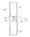
The
第1絶縁基材40は矩形の板状に形成され、上面(第1主面)、及び第1主面の反対側の下面(第2主面)を有する。第1絶縁基材40は、例えば略直方体であるが、これに限らない。例えば、円板状であってもよいし、あるいは断面が円弧状に湾曲したものであってもよい。好ましくは、第1絶縁基材40は、RFタグ100を取り付ける位置における固定治具300の表面形状に応じた形状を有する。 The first insulating
図4に示すように、第1導波素子20は第1絶縁基材40の上面に設けられている。図5に示すように、第2導波素子30は第1絶縁基材40の下面に設けられている。第1導波素子20及び第2導波素子30は、いずれも長方形状であり、アルミ等の金属薄膜のエッチング又はパターン印刷等によって形成される。 As shown in FIG. 4, the
第1導波素子20と第2導波素子30は同一形状である。なお、本願において「同一形状」とは、厳密な意味での同一に限られるものではなく、アンテナの構造に起因して僅かな差異が生じる場合も「同一形状」に含むものとする。例えば、後述のICチップ80を第1導波素子20と同一平面上に設ける場合、ICチップ80を配置するために、図4に示すように、例えば四角形状の第1導波素子20の一部に凹部25を設ける必要がある。この場合、第1導波素子20と第2導波素子30の形状は厳密には同一ではない。しかし、第1導波素子20は第2導波素子30と同様の四角形状であるので、第1導波素子20と第2導波素子30は同一形状であるというものとする。 The
給電部50は、第1絶縁基材40の側面に設けられ、第2導波素子30にその一端が電気的に接続されている。短絡部60は、第1絶縁基材40の側面に設けられ、第1導波素子20にその一端が電気的に接続され、第2導波素子30にその他端が電気的に接続されている。
図4に示すように、給電部50及び短絡部60は、第1導波素子20と第2導波素子30とに架け渡されるようにシート70上に互いに間隔をおいて並行に設けられる部材である。The
As shown in FIG. 4, the feeding
なお、給電部50及び短絡部60は、互いに並行に設けられなくてもよい。また、給電部50及び短絡部60は、第1導波素子20及び第2導波素子30を形成する際にそれたと同時に一体に形成してもよい。あるいは、給電部50及び短絡部60を別体に成形した後、各々の端部を第1導波素子20及び第2導波素子30に接合してもよい。 Note that the
図4、図5及び図6に示すように、第1導波素子20、第2導波素子30、給電部50及び短絡部60は、絶縁性のシート70上に形成されており、第1絶縁基材40の辺の部分で折り曲げられたシート70を介して第1絶縁基材40の外面に貼り付けられている。
つまり、図6に示すように、片面に第1導波素子20、第2導波素子30、給電部50及び短絡部60が形成された可撓性のシート70を、給電部50及び短絡部60の部分でともに屈曲させて第1絶縁基材40の表裏面に貼り付けることにより容易にアンテナ10を製造することができる。As shown in FIGS. 4, 5, and 6, the
That is, as shown in FIG. 6, a
なお、シート70の材料としては、PET、ポリイミド、ポリ塩化ビニルなど可撓性を有する絶縁材料を用いることが可能である。シート70の厚さは特に限定されるものではないが、一般的には数十μm程度である。また、各導波素子20,30の表面に絶縁被膜処理を施してもよい。 As the material of the
また、第1導波素子20及び第2導波素子30をシート70(基材)上に形成しているが、必ずしもシート70上に形成されたものである必要はない。例えば、第1導波素子20及び第2導波素子30を単体で形成してもよい。あるいは、第1導波素子20及び第2導波素子30をシート70上に形成した後で当該シート70を剥がしてもよい。 Also, although the
上記の第1絶縁基材40、第1導波素子20、第2導波素子30、給電部50及び短絡部60により、板状逆Fアンテナが構成される。この板状逆Fアンテナは、読取装置(図示せず)から送信された電波を受信する。第1導波素子20が電波を吸収する場合には、第2導波素子30が導体地板として働く。
一方、第2導波素子30が電波を吸収する場合には、第1導波素子20が導体地板として働く。すなわち、導波素子20,30は、RFタグ100の使用態様に応じて、導波素子と導体地板のどちらの機能も果たすことが可能である。The first insulating
On the other hand, when the
図4に示すように、第1導波素子20は、その周囲の側辺20a乃至20fの長さの合計Aがλ/4、λ/2、3λ/4、5λ/8のいずれかになるように設計されている。ここで、λは読取装置から送信された電波の波長である。なお、電波の波長λは、RFタグ100として使用可能な範囲内であれば特に限定されない。図5に示すように、第2導波素子30は、その周囲の側辺30a乃至30dの長さの合計Bが合計Aとほぼ等しくなるように設計されている。 As shown in FIG. 4, the
上記のように、第1導波素子20と第2導波素子30とは同一形状であり、各導波素子20,30の周囲の側辺の長さの合計A,Bはλ/4、λ/2、3λ/4、5λ/8のいずれかにほぼ等しい。これにより、板状逆Fアンテナの共振周波数を容易に設定することができる。 As described above, the
なお、各導波素子20,30の周囲の側辺の長さの合計A,Bが上記値のいずれかであれば、各導波素子20,30の平面形状は長方形状に限られない、例えば、各導波素子20,30の中心部を切り取ったロ字状にしてもよい。 It should be noted that the planar shape of each
また、第1絶縁基材40として絶縁体を用いてもよい。これにより、ある程度の大きさの開口面積を確保し、板状逆Fアンテナの感度向上を図ることができる。例えば、第1絶縁基材40として発泡スチロールを使用することが可能である。 Alternatively, an insulator may be used as the first insulating
また、第1絶縁基材40は誘電体であってもよい。第1絶縁基材40として、例えば比誘電率が1以上20以下の誘電体を用いることができる。誘電率が大きい誘電体(例えばセラミック)を用いた場合、コンデンサ93の静電容量が大きくなるため、第1導波素子20及び第2導波素子30の開口面積が小さくなり、RFタグ100を小型化することができる。ただし、アンテナ10の利得が小さくなるため、読取装置との間で通信可能な距離(通信距離)が短くなる。数メートル以上といった比較的長い通信距離が必要な場合は、第1絶縁基材40として誘電率が小さい誘電体を用いる。この場合、比誘電率は5以下であることが好ましい。 Also, the first insulating
上記構成のアンテナ10では、読取装置から送信され、上記の板状逆Fアンテナで受信される電波の周波数帯域で共振する共振回路が構成される。この共振回路は、インダクタパターンLとコンデンサ(第1コンデンサ)93と、により構成される(図7参照)。
ここで、インダクタパターンLは、第1導波素子20、短絡部60、第2導波素子30及び給電部50により構成され、コンデンサ93は、第1導波素子20、第2導波素子30及び第1絶縁基材40により構成される。この共振回路によって、読取装置から送信された電波(搬送波)を板状逆Fアンテナが高感度で受信できるようになるため、RFタグ100の読み取り性能を向上させることができる。さらに、後述のICチップ80が生成する電源電圧を高くすることができる。The
Here, the inductor pattern L is composed of the
(アンテナの製造方法)
次に、アンテナ10の製造方法について説明する。
まず、図6に示すように、給電部50及び短絡部60の長手方向に直交する方向Hに沿って、給電部50及び短絡部60をそれぞれ、第1導波素子20及び第2導波素子30との接合箇所近傍において折り曲げて、第1導波素子20と第2導波素子30とを対向させる。
次に、第1導波素子20を第1絶縁基材40の上面に接着剤等で貼り付け、第2導波素子30を第1絶縁基材40の下面に貼り付ける。これにより、アンテナ10としての板状逆Fアンテナを製造できる。(Antenna manufacturing method)
Next, a method for manufacturing the
First, as shown in FIG. 6, along the direction H orthogonal to the longitudinal direction of the feeding
Next, the
板状逆Fアンテナとして機能するアンテナ10は、上記のように、給電部50及び短絡部60を屈曲させて、第1絶縁基材40の表面及び裏面に第1導波素子20及び第2導波素子30をそれぞれ貼り付けることにより作製される。したがって、給電用の同軸線路またはストリップ線路を設ける従来のパッチアンテナの場合と比較して、アンテナの構造を簡略化でき、製造コストを抑えることができる。 The
(ICチップ)
ICチップ80は、図4に示すように、第1導波素子20と給電部50との間に設けられている。ICチップ80は、第1絶縁基材40の上面側(第1導波素子20と同一平面上)に配置されている。
なお、板状逆Fアンテナとして機能する範囲内であれば、ICチップ80を第1絶縁基材40の側面に配置してもよい。また、ICチップ80に外部電源を接続して、当該外部電源から供給される電圧によりICチップ80が動作するようにしてもよい。(IC chip)
The
Note that the
ICチップ80は、アンテナ10の板状逆Fアンテナが受信した読取装置の電波に基づいて動作する。
具体的には、ICチップ80は、まず、読取装置から送信される搬送波の一部を整流し、ICチップ自身が動作するために必要な電源電圧を生成する。そして、ICチップ80は、生成した電源電圧によって、ICチップ80内の制御用の論理回路、パイプ200(金属資材)の固有情報等が格納された不揮発性メモリを動作させる。
また、ICチップ80は、読取装置との間でデータの送受信を行うための通信回路等を動作させる。The
Specifically, the
The
ICチップ80には、内部にコンデンサを含むものがあり、また、ICチップ80は浮遊容量を有する。このため、共振回路の共振周波数を設定する際、ICチップ80内部の等価容量を考慮することが好ましい。換言すれば、共振回路は、インダクタパターンLのインダクタンス、コンデンサ93の静電容量、及びICチップ80内部の等価容量を考慮して設定された共振周波数を有することが好ましい。さらに、後述するように第2のコンデンサの静電容量が考慮される。 Some IC chips 80 include a capacitor inside, and the
このように、RFタグ100は、アンテナ10及びICチップ80を備えている。RFタグ100は、読取装置から送信された電波(搬送波)をRFタグ100のアンテナ10で受信する。そして、ICチップ80に記録されているパイプ200の識別データ等を反射波に乗せて読取装置へ返送する。これにより、読取装置をRFタグ100に接触させることなく、RFタグ100は読取装置と通信することが可能である。 Thus, the
(RFタグ装置110の高圧配管200への取り付け)
上記構成のRFタグ装置110を高圧配管200へ取り付けるには、次のように行うことができる。(Attachment of
The
図1に示すように、高圧配管200の開口部内に一対の係止片330を挿入して係止させることでRFタグ装置110を高圧配管200の開口端部210に容易に取り付けることができる。 As shown in FIG. 1, the
固定治具300を高圧配管200に取り付ける場合に、係止片330は高圧配管200の内周面から外周面方向に付勢する付勢部材からなるものが好ましい。係止片330はまた弾性を有しているのが好ましい。
一対の係止片330を高圧配管200の開口部内に挿入する際に、一対の係止片330が内側へ弾性変形することで、一対の係止片330を高圧配管200の内面に沿ってスライドさせ、図1に示すように高圧配管200内周面に係止させることができる。When the fixing
When the pair of locking
固定治具300を高圧配管200に取り付けた後では、一対の係止片330の復元力によって係止片330が高圧配管200の内周面に圧接する。従って、高圧配管200が外部から衝撃を受けたような場合でも固定治具300が高圧配管200から容易に外れることはない。 After the fixing
固定治具300を高圧配管200に取り付けた場合には、平板部320の周端部は高圧配管200の端面に当接して高圧配管200の開口部を実質的に閉塞する。 When the fixing
なお、高圧配管200にRFタグ装置110が取り付けられた場合に、RFタグ装置110に形成された凹部34を通して高圧配管200内の換気を行うことができる。また、凹部34を通して工具などを高圧配管200内に差し込みRFタグ装置110を高圧配管200から容易に取り外すことができる。 In addition, when the
(等価回路)
図7は、図1に示したRFタグ装置110が取り付けられた高圧配管200の等価回路の一例を示す図である。
図7に示すように、RFタグ100の等価回路は、インダクタパターンLと、コンデンサ93と、ICチップ80とからなる。インダクタパターンL、コンデンサ93およびICチップ80は、読取装置から送信される電波の周波数帯域で共振する共振回路を構成する。
この共振回路の共振周波数f[Hz]は、式(1)により与えられる。共振周波数fの値は、読取装置から送信される電波の周波数帯域に含まれるように設定される。(Equivalent circuit)
FIG. 7 is a diagram showing an example of an equivalent circuit of the high-
As shown in FIG. 7, the equivalent circuit of the
The resonance frequency f [Hz] of this resonance circuit is given by equation (1). The value of the resonance frequency f is set so as to be included in the frequency band of radio waves transmitted from the reader.

式(1)において、La:インダクタパターンLのインダクタンス、Ca:コンデンサ93の静電容量、Cb:ICチップ80内部の等価容量を意味する。 In equation (1), La means the inductance of the inductor pattern L, Ca means the electrostatic capacity of the
ここで、ICチップ80には、内部にコンデンサを含むものがあり、また、ICチップ80は浮遊容量を有する。そのため、共振回路の共振周波数fを設定する場合、ICチップ80内部の等価容量Cbを考慮することが好ましい。 Here, some
すなわち、共振回路は、インダクタパターンLのインダクタンス、コンデンサ93の静電容量、およびICチップ80の内部の等価容量Cbを考慮して設定された共振周波数fを有することが好ましい。なお、Cbとしては、例えば、使用するICチップの仕様諸元の一つとして公表されている静電容量値を用いることができる。 That is, the resonance circuit preferably has a resonance frequency f set in consideration of the inductance of the inductor pattern L, the capacitance of the
上記のように、ICチップ80内部の等価容量Cbを考慮することで、共振回路の共振周波数fを、電波の周波数帯域に精度良く設定することができる。その結果、RFタグ100の読み取り性能をさらに向上させることができる。また、ICチップ80が生成する電源電圧をさらに高くすることができる。 As described above, by considering the equivalent capacitance Cb inside the
さらに、RFタグ装置110が取り付けられた高圧配管200においては、固定治具300の平板部320にRFタグ100を電気絶縁性の貼着部材により貼着することで、コンデンサ(第2コンデンサ)270が形成され、RFタグ100のインダクタンスと共振回路を形成することができる。 Furthermore, in the high-
図7に示すように、第2コンデンサ270は、第1導波素子20、第2導波素子30及び第1絶縁基材40で構成されるコンデンサ93(第1コンデンサ)と直列に接続されている。このため、第1コンデンサ93と第2コンデンサ270の合成容量が変化して、RFタグ100の共振回路の共振周波数が大きく変化する可能性がある。 As shown in FIG. 7, the
具体的には、コンデンサ270の容量がコンデンサ93の容量よりも非常に小さい場合には、合成容量がコンデンサ93の容量に比べて大きく低下する。このことは、RFタグ100を高圧配管200内に配置した場合、RFタグ100の共振回路の共振周波数が大きく変化して、RFタグ100の読み取り性能が低下することを意味する。 Specifically, when the capacity of
そこで、本実施形態では、コンデンサ270の容量をICチップ80内部の等価容量以上にすることができる。これにより、コンデンサ93とコンデンサ270の合成容量が大幅に低下することを防ぎ、RFタグ100の性能低下を抑制することができる。コンデンサ270の容量はICチップ80内部の等価容量の2倍以上にすることが好ましい。 Therefore, in this embodiment, the capacity of the
読取装置からの電波は、RFタグ100の一方の導波素子(第1導波素子)20により受信され、RFタグ100の第1導波素子20と、該RFタグ100の他方の第2導波素子(グランドエレメント)30との間に接続されたICチップ80の回路を通し、第2導波素子30より固定治具300を介して高圧配管200に放出される。つまり、RFタグ100と固定治具300が貼着部材からなる誘電体を介して容量結合をするため、固定治具300がアンテナとして機能する。 Radio waves from the reader are received by one waveguide element (first waveguide element) 20 of the
よって、高圧配管200全体がアンテナとなり作動することができる。このようにして、RFタグ100からの電波を、高圧配管200を介して読取装置へ送ることができ、かつ読取装置からの電波を高圧配管200を介してRFタグ100で受信することができる。
その結果、RFタグ100を確実に駆動させ、無指向性で通信距離が長いRFタグ100の読み取りを実施することができる。Therefore, the entire high-
As a result, it is possible to reliably drive the
なお、高圧配管200の開口端部に取り付けたRFタグ装置110を保護するため、該RFタグ装置110を覆うキャップを高圧配管200の端部に取り付けてもよい。キャップは電気絶縁性の部材、例えば、合成樹脂製のもので形成することができる。 In order to protect the
本発明においては、RFタグ装置110が「RFタグ装置」に相当し、RFタグ100が、「RFタグ」に相当し、ICチップ80が「ICチップ」に相当し、インダクタパターンLが「インダクタパターン」に相当し、コンデンサ93が「コンデンサ」に相当し、アンテナ10が「アンテナ」に相当し、高圧配管200が「高圧配管」、「管形状の金属資材」に相当し、固定治具300が「固定治具」に相当し、平板部320が「平板部」に相当し、係止片330が「係止片」に相当する。 In the present invention, the
本発明の好ましい一実施の形態は上記の通りであるが、本発明はそれだけに制限されない。本発明の精神と範囲から逸脱することのない様々な実施形態が他になされることは理解されよう。さらに、本実施形態において、本発明の構成による作用および効果を述べているが、これら作用および効果は、一例であり、本発明を限定するものではない。 Although one preferred embodiment of the invention is described above, the invention is not so limited. It is understood that various other embodiments can be made without departing from the spirit and scope of the invention. Furthermore, in this embodiment, the actions and effects of the configuration of the present invention are described, but these actions and effects are examples and do not limit the present invention.
10 アンテナ
20 第1導波素子
30 第2導波素子
50 給電部
60 短絡部
80 ICチップ
93 コンデンサ
100 RFタグ
110 RFタグ装置
200 高圧配管
300 固定治具
320 平板部
330 係止片
REFERENCE SIGNS
Claims (3)
Translated fromJapanese前記RFタグ装置は、
固定治具と、
RFタグと、を含み、
前記RFタグは、アンテナと、
読取装置から送信された電波に基づいて動作するICチップと、を含み、
前記固定治具は、前記管形状を有する金属資材の開口端部に取り付けられる平板部と、
前記平板部の裏面から前記管形状を有する金属資材内へ延設されるとともに前記管形状を有する金属資材の内周面に係止する1または複数の係止片と、を有し、
前記アンテナは、
絶縁層を介して設けられた第1導波素子及び第2導波素子と、
前記第2導波素子に一端が電気的に接続された給電部と、
前記第1導波素子に一端が電気的に接続され、前記第2導波素子に他端が電気的に接続された短絡部と、を含み、
前記絶縁層、前記第1導波素子、前記第2導波素子、前記給電部及び前記短絡部により、前記読取装置から送信された電波を受信するように構成され、
前記第1導波素子、前記短絡部、前記第2導波素子及び前記給電部により構成されるインダクタパターンと、前記第1導波素子、前記第2導波素子及び前記絶縁層により構成されるコンデンサとにより、前記電波の周波数帯域で共振する共振回路が構成され、
前記平板部の表面に前記RFタグを固定する、RFタグ装置。An RF tag device attached to a metal material having a tubular shape,
The RF tag device
a fixture;
an RF tag;
The RF tag includes an antenna,
an IC chip that operates based on radio waves transmitted from the reading device,
The fixing jig includes a flat plate portion attached to an open end portion of the metal material having a tubular shape;
one or more locking pieces extending from the back surface of the flat plate portion into the metal material having the tubular shape and being locked to the inner peripheral surface of the metal material having the tubular shape;
The antenna is
a first waveguide element and a second waveguide element provided via an insulating layer;
a feeding section having one end electrically connected to the second waveguide element;
a short circuit part having one end electrically connected to the first waveguide element and the other end electrically connected to the second waveguide element;
configured to receive radio waves transmitted from the reading device by the insulating layer, the first waveguide element, the second waveguide element, the power supply section, and the short circuit section;
An inductor pattern composed of the first waveguide element, the short-circuit portion, the second waveguide element and the feeding portion, and composed of the first waveguide element, the second waveguide element and the insulating layer. The capacitor constitutes a resonant circuit that resonates in the frequency band of the radio waves,
An RF tag device, wherein the RF tag is fixed to the surface of the flat plate portion.
3. The RF tag device according to claim 1, wherein said metal material is high-pressure piping.
Applications Claiming Priority (3)
| Application Number | Priority Date | Filing Date | Title |
|---|---|---|---|
| JP2017155949 | 2017-08-10 | ||
| JP2017155949 | 2017-08-10 | ||
| PCT/JP2018/029703WO2019031536A1 (en) | 2017-08-10 | 2018-08-08 | Rf tag device |
Publications (2)
| Publication Number | Publication Date |
|---|---|
| JPWO2019031536A1 JPWO2019031536A1 (en) | 2020-09-03 |
| JP7121403B2true JP7121403B2 (en) | 2022-08-18 |
Family
ID=65271075
Family Applications (1)
| Application Number | Title | Priority Date | Filing Date |
|---|---|---|---|
| JP2019535695AActiveJP7121403B2 (en) | 2017-08-10 | 2018-08-08 | RF tag device |
Country Status (2)
| Country | Link |
|---|---|
| JP (1) | JP7121403B2 (en) |
| WO (1) | WO2019031536A1 (en) |
Citations (3)
| Publication number | Priority date | Publication date | Assignee | Title |
|---|---|---|---|---|
| JP2007031135A (en) | 2005-07-29 | 2007-02-08 | Taisei Corp | Single pipe processing equipment |
| JP2009199353A (en) | 2008-02-21 | 2009-09-03 | Star Engineering Co Ltd | Container with non-contact id identification apparatus and method for manufacturing the container |
| JP2011123789A (en) | 2009-12-14 | 2011-06-23 | Toray Ind Inc | Film sheet core having ic tag provided on inside wall of the core, roll, and management method of the same |
- 2018
- 2018-08-08WOPCT/JP2018/029703patent/WO2019031536A1/ennot_activeCeased
- 2018-08-08JPJP2019535695Apatent/JP7121403B2/enactiveActive
Patent Citations (3)
| Publication number | Priority date | Publication date | Assignee | Title |
|---|---|---|---|---|
| JP2007031135A (en) | 2005-07-29 | 2007-02-08 | Taisei Corp | Single pipe processing equipment |
| JP2009199353A (en) | 2008-02-21 | 2009-09-03 | Star Engineering Co Ltd | Container with non-contact id identification apparatus and method for manufacturing the container |
| JP2011123789A (en) | 2009-12-14 | 2011-06-23 | Toray Ind Inc | Film sheet core having ic tag provided on inside wall of the core, roll, and management method of the same |
Also Published As
| Publication number | Publication date |
|---|---|
| WO2019031536A1 (en) | 2019-02-14 |
| JPWO2019031536A1 (en) | 2020-09-03 |
Similar Documents
| Publication | Publication Date | Title |
|---|---|---|
| JP4452865B2 (en) | Wireless IC tag device and RFID system | |
| JP6705116B2 (en) | RF tag antenna, manufacturing method thereof, and RF tag | |
| US8618995B2 (en) | Metal pipe managed by wireless tag and wireless tag | |
| JP4681506B2 (en) | IC tag | |
| EP1981122A1 (en) | RFID tag | |
| KR100983571B1 (en) | Tag Antenna and RDF Tags | |
| JP4927665B2 (en) | Auxiliary antenna for RFID tag and its mounting method | |
| JP6872266B2 (en) | RF tag antenna, RF tag and RF tag antenna manufacturing method | |
| JP7121403B2 (en) | RF tag device | |
| CN108460306B (en) | Long-distance 360-degree wide-angle RFID reader | |
| JP2003298464A (en) | Wireless communication apparatus | |
| JP6670500B2 (en) | RF tag antenna and RF tag | |
| JP7045087B2 (en) | Fixing jig for RF tag | |
| JPWO2007017967A1 (en) | Wireless IC tag | |
| JP6831572B2 (en) | Fixing jig for RF tag | |
| JP7360292B2 (en) | Contactless data receiver/transmitter | |
| JP7133232B2 (en) | Parts management card and parts management device | |
| JP2020184653A (en) | Antenna member and RFID tag | |
| JP2008217522A (en) | Radio tag | |
| WO2019225526A1 (en) | Rf tag antenna, rf tag and rf tag with conductor | |
| JP2024033152A (en) | RFID cover with waveguide function and RFID tag set | |
| KR100906915B1 (en) | antenna | |
| JP2008129748A (en) | Non-contact IC tag and non-contact IC tag connecting body | |
| JP2016091241A (en) | Frequency adjustment method for contactless data receiving and transmitting body |
Legal Events
| Date | Code | Title | Description |
|---|---|---|---|
| A621 | Written request for application examination | Free format text:JAPANESE INTERMEDIATE CODE: A621 Effective date:20210709 | |
| A131 | Notification of reasons for refusal | Free format text:JAPANESE INTERMEDIATE CODE: A131 Effective date:20220308 | |
| A521 | Request for written amendment filed | Free format text:JAPANESE INTERMEDIATE CODE: A523 Effective date:20220408 | |
| TRDD | Decision of grant or rejection written | ||
| A01 | Written decision to grant a patent or to grant a registration (utility model) | Free format text:JAPANESE INTERMEDIATE CODE: A01 Effective date:20220726 | |
| A61 | First payment of annual fees (during grant procedure) | Free format text:JAPANESE INTERMEDIATE CODE: A61 Effective date:20220729 | |
| R150 | Certificate of patent or registration of utility model | Ref document number:7121403 Country of ref document:JP Free format text:JAPANESE INTERMEDIATE CODE: R150 | |
| R250 | Receipt of annual fees | Free format text:JAPANESE INTERMEDIATE CODE: R250 |