JP7112383B2 - Display panel manufacturing method - Google Patents
Display panel manufacturing methodDownload PDFInfo
- Publication number
- JP7112383B2 JP7112383B2JP2019500048AJP2019500048AJP7112383B2JP 7112383 B2JP7112383 B2JP 7112383B2JP 2019500048 AJP2019500048 AJP 2019500048AJP 2019500048 AJP2019500048 AJP 2019500048AJP 7112383 B2JP7112383 B2JP 7112383B2
- Authority
- JP
- Japan
- Prior art keywords
- film
- light
- conductive film
- pixel
- display
- Prior art date
- Legal status (The legal status is an assumption and is not a legal conclusion. Google has not performed a legal analysis and makes no representation as to the accuracy of the status listed.)
- Active
Links
- 238000004519manufacturing processMethods0.000titledescription28
- 239000010408filmSubstances0.000description965
- 230000006870functionEffects0.000description150
- 239000000463materialSubstances0.000description149
- 239000010410layerSubstances0.000description130
- 239000004065semiconductorSubstances0.000description97
- 239000000758substrateSubstances0.000description97
- 238000000034methodMethods0.000description85
- 238000001514detection methodMethods0.000description60
- 230000010365information processingEffects0.000description57
- 238000010586diagramMethods0.000description42
- XLOMVQKBTHCTTD-UHFFFAOYSA-NZinc monoxideChemical compound[Zn]=OXLOMVQKBTHCTTD-UHFFFAOYSA-N0.000description38
- 229910052738indiumInorganic materials0.000description37
- XUIMIQQOPSSXEZ-UHFFFAOYSA-NSiliconChemical compound[Si]XUIMIQQOPSSXEZ-UHFFFAOYSA-N0.000description36
- 229910052710siliconInorganic materials0.000description36
- 239000010703siliconSubstances0.000description36
- 239000011701zincSubstances0.000description33
- APFVFJFRJDLVQX-UHFFFAOYSA-Nindium atomChemical compound[In]APFVFJFRJDLVQX-UHFFFAOYSA-N0.000description31
- 239000004973liquid crystal related substanceSubstances0.000description30
- 229910052760oxygenInorganic materials0.000description30
- 238000012545processingMethods0.000description30
- 229910052751metalInorganic materials0.000description29
- QVGXLLKOCUKJST-UHFFFAOYSA-Natomic oxygenChemical compound[O]QVGXLLKOCUKJST-UHFFFAOYSA-N0.000description28
- 239000001301oxygenSubstances0.000description28
- 230000003287optical effectEffects0.000description26
- IJGRMHOSHXDMSA-UHFFFAOYSA-NAtomic nitrogenChemical compoundN#NIJGRMHOSHXDMSA-UHFFFAOYSA-N0.000description25
- 239000002184metalSubstances0.000description23
- 239000004020conductorSubstances0.000description21
- 229920005989resinPolymers0.000description21
- 239000011347resinSubstances0.000description21
- 239000010936titaniumSubstances0.000description20
- 238000004891communicationMethods0.000description19
- 239000007789gasSubstances0.000description19
- 229910044991metal oxideInorganic materials0.000description19
- 239000011787zinc oxideSubstances0.000description19
- RTAQQCXQSZGOHL-UHFFFAOYSA-NTitaniumChemical compound[Ti]RTAQQCXQSZGOHL-UHFFFAOYSA-N0.000description18
- 229910052719titaniumInorganic materials0.000description18
- 238000005530etchingMethods0.000description17
- 230000008569processEffects0.000description17
- 229910052725zincInorganic materials0.000description16
- 238000009792diffusion processMethods0.000description15
- HCHKCACWOHOZIP-UHFFFAOYSA-NZincChemical compound[Zn]HCHKCACWOHOZIP-UHFFFAOYSA-N0.000description14
- 230000005540biological transmissionEffects0.000description14
- 229920001721polyimidePolymers0.000description14
- 238000002834transmittanceMethods0.000description14
- 229910052581Si3N4Inorganic materials0.000description13
- 229910052782aluminiumInorganic materials0.000description13
- XAGFODPZIPBFFR-UHFFFAOYSA-NaluminiumChemical compound[Al]XAGFODPZIPBFFR-UHFFFAOYSA-N0.000description13
- 239000003990capacitorSubstances0.000description13
- 239000001257hydrogenSubstances0.000description13
- 229910052739hydrogenInorganic materials0.000description13
- 239000012535impuritySubstances0.000description13
- 239000002648laminated materialSubstances0.000description13
- 239000011368organic materialSubstances0.000description13
- HQVNEWCFYHHQES-UHFFFAOYSA-Nsilicon nitrideChemical compoundN12[Si]34N5[Si]62N3[Si]51N64HQVNEWCFYHHQES-UHFFFAOYSA-N0.000description13
- 229910052721tungstenInorganic materials0.000description13
- 239000010937tungstenSubstances0.000description13
- XKRFYHLGVUSROY-UHFFFAOYSA-NArgonChemical compound[Ar]XKRFYHLGVUSROY-UHFFFAOYSA-N0.000description12
- 239000004642PolyimideSubstances0.000description12
- 239000002131composite materialSubstances0.000description12
- 229910010272inorganic materialInorganic materials0.000description12
- 239000011147inorganic materialSubstances0.000description12
- 239000002346layers by functionSubstances0.000description12
- 229910052757nitrogenInorganic materials0.000description12
- UFHFLCQGNIYNRP-UHFFFAOYSA-NHydrogenChemical compound[H][H]UFHFLCQGNIYNRP-UHFFFAOYSA-N0.000description11
- ATJFFYVFTNAWJD-UHFFFAOYSA-NTinChemical compound[Sn]ATJFFYVFTNAWJD-UHFFFAOYSA-N0.000description11
- 239000013078crystalSubstances0.000description11
- 229910052733galliumInorganic materials0.000description11
- VYPSYNLAJGMNEJ-UHFFFAOYSA-Nsilicon dioxideInorganic materialsO=[Si]=OVYPSYNLAJGMNEJ-UHFFFAOYSA-N0.000description11
- 229910052709silverInorganic materials0.000description11
- 239000004332silverSubstances0.000description11
- 229910052718tinInorganic materials0.000description11
- WFKWXMTUELFFGS-UHFFFAOYSA-NtungstenChemical compound[W]WFKWXMTUELFFGS-UHFFFAOYSA-N0.000description11
- OKTJSMMVPCPJKN-UHFFFAOYSA-NCarbonChemical compound[C]OKTJSMMVPCPJKN-UHFFFAOYSA-N0.000description10
- XEEYBQQBJWHFJM-UHFFFAOYSA-NIronChemical compound[Fe]XEEYBQQBJWHFJM-UHFFFAOYSA-N0.000description10
- PXHVJJICTQNCMI-UHFFFAOYSA-NNickelChemical compound[Ni]PXHVJJICTQNCMI-UHFFFAOYSA-N0.000description10
- 239000011521glassSubstances0.000description10
- 239000003566sealing materialSubstances0.000description10
- 238000003860storageMethods0.000description10
- 239000004925Acrylic resinSubstances0.000description9
- 229920000178Acrylic resinPolymers0.000description9
- GYHNNYVSQQEPJS-UHFFFAOYSA-NGalliumChemical compound[Ga]GYHNNYVSQQEPJS-UHFFFAOYSA-N0.000description9
- MUBZPKHOEPUJKR-UHFFFAOYSA-NOxalic acidChemical compoundOC(=O)C(O)=OMUBZPKHOEPUJKR-UHFFFAOYSA-N0.000description9
- 230000015572biosynthetic processEffects0.000description9
- 150000004706metal oxidesChemical class0.000description9
- 238000004544sputter depositionMethods0.000description9
- RYGMFSIKBFXOCR-UHFFFAOYSA-NCopperChemical compound[Cu]RYGMFSIKBFXOCR-UHFFFAOYSA-N0.000description8
- NBIIXXVUZAFLBC-UHFFFAOYSA-NPhosphoric acidChemical compoundOP(O)(O)=ONBIIXXVUZAFLBC-UHFFFAOYSA-N0.000description8
- 229910052802copperInorganic materials0.000description8
- 239000010949copperSubstances0.000description8
- 230000005684electric fieldEffects0.000description8
- 229910021389grapheneInorganic materials0.000description8
- 229910052814silicon oxideInorganic materials0.000description8
- 238000004380ashingMethods0.000description7
- 238000004364calculation methodMethods0.000description7
- 239000000203mixtureSubstances0.000description7
- 238000001228spectrumMethods0.000description7
- 229910052715tantalumInorganic materials0.000description7
- GUVRBAGPIYLISA-UHFFFAOYSA-Ntantalum atomChemical compound[Ta]GUVRBAGPIYLISA-UHFFFAOYSA-N0.000description7
- MYMOFIZGZYHOMD-UHFFFAOYSA-NDioxygenChemical compoundO=OMYMOFIZGZYHOMD-UHFFFAOYSA-N0.000description6
- KDLHZDBZIXYQEI-UHFFFAOYSA-NPalladiumChemical compound[Pd]KDLHZDBZIXYQEI-UHFFFAOYSA-N0.000description6
- 229910052786argonInorganic materials0.000description6
- 239000000969carrierSubstances0.000description6
- 239000003086colorantSubstances0.000description6
- 150000001875compoundsChemical class0.000description6
- 229910001882dioxygenInorganic materials0.000description6
- 230000000694effectsEffects0.000description6
- 229910003437indium oxideInorganic materials0.000description6
- PJXISJQVUVHSOJ-UHFFFAOYSA-Nindium(iii) oxideChemical compound[O-2].[O-2].[O-2].[In+3].[In+3]PJXISJQVUVHSOJ-UHFFFAOYSA-N0.000description6
- AMGQUBHHOARCQH-UHFFFAOYSA-Nindium;oxotinChemical compound[In].[Sn]=OAMGQUBHHOARCQH-UHFFFAOYSA-N0.000description6
- 239000002070nanowireSubstances0.000description6
- TWNQGVIAIRXVLR-UHFFFAOYSA-Noxo(oxoalumanyloxy)alumaneChemical compoundO=[Al]O[Al]=OTWNQGVIAIRXVLR-UHFFFAOYSA-N0.000description6
- -1polyethylene terephthalatePolymers0.000description6
- YVTHLONGBIQYBO-UHFFFAOYSA-Nzinc indium(3+) oxygen(2-)Chemical compound[O--].[Zn++].[In+3]YVTHLONGBIQYBO-UHFFFAOYSA-N0.000description6
- ZOKXTWBITQBERF-UHFFFAOYSA-NMolybdenumChemical compound[Mo]ZOKXTWBITQBERF-UHFFFAOYSA-N0.000description5
- 239000004952PolyamideSubstances0.000description5
- 239000000853adhesiveSubstances0.000description5
- 230000001070adhesive effectEffects0.000description5
- 238000006243chemical reactionMethods0.000description5
- PMHQVHHXPFUNSP-UHFFFAOYSA-Mcopper(1+);methylsulfanylmethane;bromideChemical compoundBr[Cu].CSCPMHQVHHXPFUNSP-UHFFFAOYSA-M0.000description5
- 239000005262ferroelectric liquid crystals (FLCs)Substances0.000description5
- 229910052742ironInorganic materials0.000description5
- 229910052750molybdenumInorganic materials0.000description5
- 239000011733molybdenumSubstances0.000description5
- 239000002105nanoparticleSubstances0.000description5
- 229910052759nickelInorganic materials0.000description5
- 239000000243solutionSubstances0.000description5
- XLYOFNOQVPJJNP-UHFFFAOYSA-NwaterSubstancesOXLYOFNOQVPJJNP-UHFFFAOYSA-N0.000description5
- 229910001868waterInorganic materials0.000description5
- 238000001039wet etchingMethods0.000description5
- VYZAMTAEIAYCRO-UHFFFAOYSA-NChromiumChemical compound[Cr]VYZAMTAEIAYCRO-UHFFFAOYSA-N0.000description4
- PWHULOQIROXLJO-UHFFFAOYSA-NManganeseChemical compound[Mn]PWHULOQIROXLJO-UHFFFAOYSA-N0.000description4
- 229910006404SnO 2Inorganic materials0.000description4
- NRTOMJZYCJJWKI-UHFFFAOYSA-NTitanium nitrideChemical compound[Ti]#NNRTOMJZYCJJWKI-UHFFFAOYSA-N0.000description4
- 229910000147aluminium phosphateInorganic materials0.000description4
- 238000000231atomic layer depositionMethods0.000description4
- 230000000903blocking effectEffects0.000description4
- 230000008859changeEffects0.000description4
- 239000000460chlorineSubstances0.000description4
- 229910052804chromiumInorganic materials0.000description4
- 239000011651chromiumSubstances0.000description4
- 239000000470constituentSubstances0.000description4
- 239000013256coordination polymerSubstances0.000description4
- 238000005520cutting processMethods0.000description4
- 230000006837decompressionEffects0.000description4
- 238000001312dry etchingMethods0.000description4
- 238000005401electroluminescenceMethods0.000description4
- 238000010894electron beam technologyMethods0.000description4
- MRELNEQAGSRDBK-UHFFFAOYSA-Nlanthanum(3+);oxygen(2-)Chemical compound[O-2].[O-2].[O-2].[La+3].[La+3]MRELNEQAGSRDBK-UHFFFAOYSA-N0.000description4
- 239000011572manganeseSubstances0.000description4
- PLDDOISOJJCEMH-UHFFFAOYSA-Nneodymium(3+);oxygen(2-)Chemical compound[O-2].[O-2].[O-2].[Nd+3].[Nd+3]PLDDOISOJJCEMH-UHFFFAOYSA-N0.000description4
- 150000004767nitridesChemical class0.000description4
- 150000002894organic compoundsChemical class0.000description4
- BASFCYQUMIYNBI-UHFFFAOYSA-NplatinumChemical compound[Pt]BASFCYQUMIYNBI-UHFFFAOYSA-N0.000description4
- 229920002647polyamidePolymers0.000description4
- 239000004417polycarbonateSubstances0.000description4
- 229920000515polycarbonatePolymers0.000description4
- 229920000728polyesterPolymers0.000description4
- 229920000098polyolefinPolymers0.000description4
- 239000002096quantum dotSubstances0.000description4
- 239000005341toughened glassSubstances0.000description4
- QTBSBXVTEAMEQO-UHFFFAOYSA-NAcetic acidChemical compoundCC(O)=OQTBSBXVTEAMEQO-UHFFFAOYSA-N0.000description3
- ZOXJGFHDIHLPTG-UHFFFAOYSA-NBoronChemical compound[B]ZOXJGFHDIHLPTG-UHFFFAOYSA-N0.000description3
- 102100027310Bromodomain adjacent to zinc finger domain protein 1AHuman genes0.000description3
- 229910052684CeriumInorganic materials0.000description3
- ZAMOUSCENKQFHK-UHFFFAOYSA-NChlorine atomChemical compound[Cl]ZAMOUSCENKQFHK-UHFFFAOYSA-N0.000description3
- 101000937778Homo sapiens Bromodomain adjacent to zinc finger domain protein 1AProteins0.000description3
- FYYHWMGAXLPEAU-UHFFFAOYSA-NMagnesiumChemical compound[Mg]FYYHWMGAXLPEAU-UHFFFAOYSA-N0.000description3
- 229910052779NeodymiumInorganic materials0.000description3
- 229910004298SiO 2Inorganic materials0.000description3
- QCWXUUIWCKQGHC-UHFFFAOYSA-NZirconiumChemical compound[Zr]QCWXUUIWCKQGHC-UHFFFAOYSA-N0.000description3
- 229910021417amorphous siliconInorganic materials0.000description3
- 239000012298atmosphereSubstances0.000description3
- 229910052790berylliumInorganic materials0.000description3
- ATBAMAFKBVZNFJ-UHFFFAOYSA-Nberyllium atomChemical compound[Be]ATBAMAFKBVZNFJ-UHFFFAOYSA-N0.000description3
- 229910052796boronInorganic materials0.000description3
- 239000000919ceramicSubstances0.000description3
- ZMIGMASIKSOYAM-UHFFFAOYSA-NceriumChemical compound[Ce][Ce][Ce][Ce][Ce][Ce][Ce][Ce][Ce][Ce][Ce][Ce][Ce][Ce][Ce][Ce][Ce][Ce][Ce][Ce][Ce][Ce][Ce][Ce][Ce][Ce][Ce][Ce][Ce][Ce][Ce][Ce][Ce][Ce][Ce][Ce][Ce][Ce]ZMIGMASIKSOYAM-UHFFFAOYSA-N0.000description3
- 229910052801chlorineInorganic materials0.000description3
- AJNVQOSZGJRYEI-UHFFFAOYSA-Ndigallium;oxygen(2-)Chemical compound[O-2].[O-2].[O-2].[Ga+3].[Ga+3]AJNVQOSZGJRYEI-UHFFFAOYSA-N0.000description3
- 238000000295emission spectrumMethods0.000description3
- 238000002149energy-dispersive X-ray emission spectroscopyMethods0.000description3
- 239000003822epoxy resinSubstances0.000description3
- 230000005669field effectEffects0.000description3
- 229910001195gallium oxideInorganic materials0.000description3
- 229910052732germaniumInorganic materials0.000description3
- GNPVGFCGXDBREM-UHFFFAOYSA-Ngermanium atomChemical compound[Ge]GNPVGFCGXDBREM-UHFFFAOYSA-N0.000description3
- 229910052735hafniumInorganic materials0.000description3
- VBJZVLUMGGDVMO-UHFFFAOYSA-Nhafnium atomChemical compound[Hf]VBJZVLUMGGDVMO-UHFFFAOYSA-N0.000description3
- 238000010438heat treatmentMethods0.000description3
- 238000009413insulationMethods0.000description3
- 238000003475laminationMethods0.000description3
- 229910052746lanthanumInorganic materials0.000description3
- FZLIPJUXYLNCLC-UHFFFAOYSA-Nlanthanum atomChemical compound[La]FZLIPJUXYLNCLC-UHFFFAOYSA-N0.000description3
- 229910052749magnesiumInorganic materials0.000description3
- 239000011777magnesiumSubstances0.000description3
- 238000005259measurementMethods0.000description3
- QEFYFXOXNSNQGX-UHFFFAOYSA-Nneodymium atomChemical compound[Nd]QEFYFXOXNSNQGX-UHFFFAOYSA-N0.000description3
- 235000006408oxalic acidNutrition0.000description3
- 229910052763palladiumInorganic materials0.000description3
- 239000002245particleSubstances0.000description3
- 229920000647polyepoxidePolymers0.000description3
- 229920001296polysiloxanePolymers0.000description3
- 239000010453quartzSubstances0.000description3
- 239000000126substanceSubstances0.000description3
- 229910052720vanadiumInorganic materials0.000description3
- GPPXJZIENCGNKB-UHFFFAOYSA-NvanadiumChemical compound[V]#[V]GPPXJZIENCGNKB-UHFFFAOYSA-N0.000description3
- 229910052727yttriumInorganic materials0.000description3
- VWQVUPCCIRVNHF-UHFFFAOYSA-Nyttrium atomChemical compound[Y]VWQVUPCCIRVNHF-UHFFFAOYSA-N0.000description3
- 229910052726zirconiumInorganic materials0.000description3
- 229910000881Cu alloyInorganic materials0.000description2
- 229920000089Cyclic olefin copolymerPolymers0.000description2
- YCKRFDGAMUMZLT-UHFFFAOYSA-NFluorine atomChemical compound[F]YCKRFDGAMUMZLT-UHFFFAOYSA-N0.000description2
- 229910000914Mn alloyInorganic materials0.000description2
- CBENFWSGALASAD-UHFFFAOYSA-NOzoneChemical compound[O-][O+]=OCBENFWSGALASAD-UHFFFAOYSA-N0.000description2
- BQCADISMDOOEFD-UHFFFAOYSA-NSilverChemical compound[Ag]BQCADISMDOOEFD-UHFFFAOYSA-N0.000description2
- 241001422033ThestylusSpecies0.000description2
- WGLPBDUCMAPZCE-UHFFFAOYSA-NTrioxochromiumChemical compoundO=[Cr](=O)=OWGLPBDUCMAPZCE-UHFFFAOYSA-N0.000description2
- 238000002441X-ray diffractionMethods0.000description2
- 239000002253acidSubstances0.000description2
- 229910045601alloyInorganic materials0.000description2
- 239000000956alloySubstances0.000description2
- 239000005354aluminosilicate glassSubstances0.000description2
- 239000002585baseSubstances0.000description2
- DQXBYHZEEUGOBF-UHFFFAOYSA-Nbut-3-enoic acid;etheneChemical compoundC=C.OC(=O)CC=CDQXBYHZEEUGOBF-UHFFFAOYSA-N0.000description2
- 239000003638chemical reducing agentSubstances0.000description2
- 229910000423chromium oxideInorganic materials0.000description2
- 239000010941cobaltSubstances0.000description2
- 229910017052cobaltInorganic materials0.000description2
- GUTLYIVDDKVIGB-UHFFFAOYSA-Ncobalt atomChemical compound[Co]GUTLYIVDDKVIGB-UHFFFAOYSA-N0.000description2
- 229920001940conductive polymerPolymers0.000description2
- 238000011161developmentMethods0.000description2
- 239000000428dustSubstances0.000description2
- 230000005674electromagnetic inductionEffects0.000description2
- 239000005038ethylene vinyl acetateSubstances0.000description2
- 230000001747exhibiting effectEffects0.000description2
- 238000000605extractionMethods0.000description2
- 239000011737fluorineSubstances0.000description2
- 229910052731fluorineInorganic materials0.000description2
- PCHJSUWPFVWCPO-UHFFFAOYSA-NgoldChemical compound[Au]PCHJSUWPFVWCPO-UHFFFAOYSA-N0.000description2
- 229910052737goldInorganic materials0.000description2
- 239000010931goldSubstances0.000description2
- 229910002804graphiteInorganic materials0.000description2
- 239000010439graphiteSubstances0.000description2
- 229910000449hafnium oxideInorganic materials0.000description2
- WIHZLLGSGQNAGK-UHFFFAOYSA-Nhafnium(4+);oxygen(2-)Chemical compound[O-2].[O-2].[Hf+4]WIHZLLGSGQNAGK-UHFFFAOYSA-N0.000description2
- 150000002431hydrogenChemical class0.000description2
- 238000003384imaging methodMethods0.000description2
- 229910052809inorganic oxideInorganic materials0.000description2
- 238000005468ion implantationMethods0.000description2
- 150000002500ionsChemical class0.000description2
- 230000001678irradiating effectEffects0.000description2
- 230000033001locomotionEffects0.000description2
- 229910052748manganeseInorganic materials0.000description2
- 239000011159matrix materialSubstances0.000description2
- 150000002739metalsChemical class0.000description2
- 239000011259mixed solutionSubstances0.000description2
- 239000002159nanocrystalSubstances0.000description2
- 238000001579optical reflectometryMethods0.000description2
- SIWVEOZUMHYXCS-UHFFFAOYSA-Noxo(oxoyttriooxy)yttriumChemical compoundO=[Y]O[Y]=OSIWVEOZUMHYXCS-UHFFFAOYSA-N0.000description2
- BPUBBGLMJRNUCC-UHFFFAOYSA-Noxygen(2-);tantalum(5+)Chemical compound[O-2].[O-2].[O-2].[O-2].[O-2].[Ta+5].[Ta+5]BPUBBGLMJRNUCC-UHFFFAOYSA-N0.000description2
- RVTZCBVAJQQJTK-UHFFFAOYSA-Noxygen(2-);zirconium(4+)Chemical compound[O-2].[O-2].[Zr+4]RVTZCBVAJQQJTK-UHFFFAOYSA-N0.000description2
- 230000000737periodic effectEffects0.000description2
- 229910052697platinumInorganic materials0.000description2
- 229920001200poly(ethylene-vinyl acetate)Polymers0.000description2
- 229920002037poly(vinyl butyral) polymerPolymers0.000description2
- 229920000139polyethylene terephthalatePolymers0.000description2
- 239000005020polyethylene terephthalateSubstances0.000description2
- 239000009719polyimide resinSubstances0.000description2
- 229920000915polyvinyl chloridePolymers0.000description2
- 239000004800polyvinyl chlorideSubstances0.000description2
- 230000009467reductionEffects0.000description2
- 239000005871repellentSubstances0.000description2
- 239000000523sampleSubstances0.000description2
- 229910052594sapphireInorganic materials0.000description2
- 239000010980sapphireSubstances0.000description2
- MZLGASXMSKOWSE-UHFFFAOYSA-Ntantalum nitrideChemical compound[Ta]#NMZLGASXMSKOWSE-UHFFFAOYSA-N0.000description2
- 229910001936tantalum oxideInorganic materials0.000description2
- VZGDMQKNWNREIO-UHFFFAOYSA-NtetrachloromethaneChemical compoundClC(Cl)(Cl)ClVZGDMQKNWNREIO-UHFFFAOYSA-N0.000description2
- 229910001928zirconium oxideInorganic materials0.000description2
- VXEGSRKPIUDPQT-UHFFFAOYSA-N4-[4-(4-methoxyphenyl)piperazin-1-yl]anilineChemical compoundC1=CC(OC)=CC=C1N1CCN(C=2C=CC(N)=CC=2)CC1VXEGSRKPIUDPQT-UHFFFAOYSA-N0.000description1
- 229910019974CrSiInorganic materials0.000description1
- 239000005264High molar mass liquid crystalSubstances0.000description1
- CPELXLSAUQHCOX-UHFFFAOYSA-NHydrogen bromideChemical compoundBrCPELXLSAUQHCOX-UHFFFAOYSA-N0.000description1
- 229910016006MoSiInorganic materials0.000description1
- GRYLNZFGIOXLOG-UHFFFAOYSA-NNitric acidChemical compoundO[N+]([O-])=OGRYLNZFGIOXLOG-UHFFFAOYSA-N0.000description1
- 239000004677NylonSubstances0.000description1
- 229920012266Poly(ether sulfone) PESPolymers0.000description1
- 239000004983Polymer Dispersed Liquid CrystalSubstances0.000description1
- KWYUFKZDYYNOTN-UHFFFAOYSA-MPotassium hydroxideChemical compound[OH-].[K+]KWYUFKZDYYNOTN-UHFFFAOYSA-M0.000description1
- 229910018503SF6Inorganic materials0.000description1
- 229910003902SiCl 4Inorganic materials0.000description1
- BLRPTPMANUNPDV-UHFFFAOYSA-NSilaneChemical compound[SiH4]BLRPTPMANUNPDV-UHFFFAOYSA-N0.000description1
- 229910000577Silicon-germaniumInorganic materials0.000description1
- 239000004990Smectic liquid crystalSubstances0.000description1
- 239000004974Thermotropic liquid crystalSubstances0.000description1
- LEVVHYCKPQWKOP-UHFFFAOYSA-N[Si].[Ge]Chemical compound[Si].[Ge]LEVVHYCKPQWKOP-UHFFFAOYSA-N0.000description1
- 230000002159abnormal effectEffects0.000description1
- 238000010521absorption reactionMethods0.000description1
- 230000001133accelerationEffects0.000description1
- 239000000654additiveSubstances0.000description1
- 230000000996additive effectEffects0.000description1
- 229910052783alkali metalInorganic materials0.000description1
- 150000001340alkali metalsChemical class0.000description1
- 229910052784alkaline earth metalInorganic materials0.000description1
- 150000001342alkaline earth metalsChemical class0.000description1
- 238000004458analytical methodMethods0.000description1
- 239000004760aramidSubstances0.000description1
- 229920003235aromatic polyamidePolymers0.000description1
- 229910000420cerium oxideInorganic materials0.000description1
- 238000005229chemical vapour depositionMethods0.000description1
- 230000003098cholesteric effectEffects0.000description1
- 238000004040coloringMethods0.000description1
- 230000000295complement effectEffects0.000description1
- 229920001577copolymerPolymers0.000description1
- 238000012937correctionMethods0.000description1
- 230000007547defectEffects0.000description1
- 238000000151depositionMethods0.000description1
- 230000008021depositionEffects0.000description1
- 230000006866deteriorationEffects0.000description1
- 238000007865dilutingMethods0.000description1
- 229910001873dinitrogenInorganic materials0.000description1
- 239000006185dispersionSubstances0.000description1
- 238000005516engineering processMethods0.000description1
- 230000007274generation of a signal involved in cell-cell signalingEffects0.000description1
- YBMRDBCBODYGJE-UHFFFAOYSA-Ngermanium oxideInorganic materialsO=[Ge]=OYBMRDBCBODYGJE-UHFFFAOYSA-N0.000description1
- 230000003760hair shineEffects0.000description1
- 230000020169heat generationEffects0.000description1
- 239000001307heliumSubstances0.000description1
- 229910052734heliumInorganic materials0.000description1
- SWQJXJOGLNCZEY-UHFFFAOYSA-Nhelium atomChemical compound[He]SWQJXJOGLNCZEY-UHFFFAOYSA-N0.000description1
- 239000012943hotmeltSubstances0.000description1
- 150000003949imidesChemical class0.000description1
- 238000007654immersionMethods0.000description1
- 230000001771impaired effectEffects0.000description1
- 239000011261inert gasSubstances0.000description1
- 238000002347injectionMethods0.000description1
- 239000007924injectionSubstances0.000description1
- 239000011229interlayerSubstances0.000description1
- 238000010030laminatingMethods0.000description1
- 239000005355lead glassSubstances0.000description1
- 238000001459lithographyMethods0.000description1
- 239000000395magnesium oxideSubstances0.000description1
- CPLXHLVBOLITMK-UHFFFAOYSA-Nmagnesium oxideInorganic materials[Mg]=OCPLXHLVBOLITMK-UHFFFAOYSA-N0.000description1
- AXZKOIWUVFPNLO-UHFFFAOYSA-Nmagnesium;oxygen(2-)Chemical compound[O-2].[Mg+2]AXZKOIWUVFPNLO-UHFFFAOYSA-N0.000description1
- 238000013507mappingMethods0.000description1
- 238000000691measurement methodMethods0.000description1
- 239000012528membraneSubstances0.000description1
- 239000011156metal matrix compositeSubstances0.000description1
- UNRFQJSWBQGLDR-UHFFFAOYSA-Nmethane trihydrofluorideChemical compoundC.F.F.FUNRFQJSWBQGLDR-UHFFFAOYSA-N0.000description1
- 238000013508migrationMethods0.000description1
- 230000005012migrationEffects0.000description1
- 238000012986modificationMethods0.000description1
- 230000004048modificationEffects0.000description1
- QKCGXXHCELUCKW-UHFFFAOYSA-Nn-[4-[4-(dinaphthalen-2-ylamino)phenyl]phenyl]-n-naphthalen-2-ylnaphthalen-2-amineChemical compoundC1=CC=CC2=CC(N(C=3C=CC(=CC=3)C=3C=CC(=CC=3)N(C=3C=C4C=CC=CC4=CC=3)C=3C=C4C=CC=CC4=CC=3)C3=CC4=CC=CC=C4C=C3)=CC=C21QKCGXXHCELUCKW-UHFFFAOYSA-N0.000description1
- 229910017604nitric acidInorganic materials0.000description1
- 229920001778nylonPolymers0.000description1
- 239000005416organic matterSubstances0.000description1
- 230000001151other effectEffects0.000description1
- 230000003647oxidationEffects0.000description1
- 238000007254oxidation reactionMethods0.000description1
- BMMGVYCKOGBVEV-UHFFFAOYSA-Noxo(oxoceriooxy)ceriumChemical compound[Ce]=O.O=[Ce]=OBMMGVYCKOGBVEV-UHFFFAOYSA-N0.000description1
- PVADDRMAFCOOPC-UHFFFAOYSA-NoxogermaniumChemical compound[Ge]=OPVADDRMAFCOOPC-UHFFFAOYSA-N0.000description1
- 239000005011phenolic resinSubstances0.000description1
- 229920002120photoresistant polymerPolymers0.000description1
- 230000000704physical effectEffects0.000description1
- 239000011295pitchSubstances0.000description1
- 238000009832plasma treatmentMethods0.000description1
- 229920003023plasticPolymers0.000description1
- 239000004033plasticSubstances0.000description1
- 229920006122polyamide resinPolymers0.000description1
- 229920005668polycarbonate resinPolymers0.000description1
- 239000004431polycarbonate resinSubstances0.000description1
- 229910021420polycrystalline siliconInorganic materials0.000description1
- 229920001225polyester resinPolymers0.000description1
- 239000011112polyethylene naphthalateSubstances0.000description1
- 229920005672polyolefin resinPolymers0.000description1
- 229920005591polysiliconPolymers0.000description1
- 229920002635polyurethanePolymers0.000description1
- 239000004814polyurethaneSubstances0.000description1
- 229940072033potashDrugs0.000description1
- BWHMMNNQKKPAPP-UHFFFAOYSA-Lpotassium carbonateSubstances[K+].[K+].[O-]C([O-])=OBWHMMNNQKKPAPP-UHFFFAOYSA-L0.000description1
- 235000015320potassium carbonateNutrition0.000description1
- 238000003672processing methodMethods0.000description1
- 239000000565sealantSubstances0.000description1
- 229910000077silaneInorganic materials0.000description1
- HBMJWWWQQXIZIP-UHFFFAOYSA-Nsilicon carbideChemical compound[Si+]#[C-]HBMJWWWQQXIZIP-UHFFFAOYSA-N0.000description1
- 229910010271silicon carbideInorganic materials0.000description1
- 239000005049silicon tetrachlorideSubstances0.000description1
- 229920002050silicone resinPolymers0.000description1
- 239000002356single layerSubstances0.000description1
- 239000005361soda-lime glassSubstances0.000description1
- 239000007787solidSubstances0.000description1
- 238000004528spin coatingMethods0.000description1
- 239000010935stainless steelSubstances0.000description1
- 229910001220stainless steelInorganic materials0.000description1
- SFZCNBIFKDRMGX-UHFFFAOYSA-Nsulfur hexafluorideChemical compoundFS(F)(F)(F)(F)FSFZCNBIFKDRMGX-UHFFFAOYSA-N0.000description1
- 229960000909sulfur hexafluorideDrugs0.000description1
- TXEYQDLBPFQVAA-UHFFFAOYSA-NtetrafluoromethaneChemical compoundFC(F)(F)FTXEYQDLBPFQVAA-UHFFFAOYSA-N0.000description1
- 229920001187thermosetting polymerPolymers0.000description1
- 239000010409thin filmSubstances0.000description1
- FAQYAMRNWDIXMY-UHFFFAOYSA-NtrichloroboraneChemical compoundClB(Cl)ClFAQYAMRNWDIXMY-UHFFFAOYSA-N0.000description1
- 239000002699waste materialSubstances0.000description1
- 239000002023woodSubstances0.000description1
Images


Classifications
- G—PHYSICS
- G09—EDUCATION; CRYPTOGRAPHY; DISPLAY; ADVERTISING; SEALS
- G09F—DISPLAYING; ADVERTISING; SIGNS; LABELS OR NAME-PLATES; SEALS
- G09F9/00—Indicating arrangements for variable information in which the information is built-up on a support by selection or combination of individual elements
- G09F9/30—Indicating arrangements for variable information in which the information is built-up on a support by selection or combination of individual elements in which the desired character or characters are formed by combining individual elements
- H—ELECTRICITY
- H05—ELECTRIC TECHNIQUES NOT OTHERWISE PROVIDED FOR
- H05B—ELECTRIC HEATING; ELECTRIC LIGHT SOURCES NOT OTHERWISE PROVIDED FOR; CIRCUIT ARRANGEMENTS FOR ELECTRIC LIGHT SOURCES, IN GENERAL
- H05B33/00—Electroluminescent light sources
- H05B33/10—Apparatus or processes specially adapted to the manufacture of electroluminescent light sources
- H—ELECTRICITY
- H05—ELECTRIC TECHNIQUES NOT OTHERWISE PROVIDED FOR
- H05B—ELECTRIC HEATING; ELECTRIC LIGHT SOURCES NOT OTHERWISE PROVIDED FOR; CIRCUIT ARRANGEMENTS FOR ELECTRIC LIGHT SOURCES, IN GENERAL
- H05B33/00—Electroluminescent light sources
- H05B33/12—Light sources with substantially two-dimensional radiating surfaces
- H05B33/14—Light sources with substantially two-dimensional radiating surfaces characterised by the chemical or physical composition or the arrangement of the electroluminescent material, or by the simultaneous addition of the electroluminescent material in or onto the light source
- H—ELECTRICITY
- H05—ELECTRIC TECHNIQUES NOT OTHERWISE PROVIDED FOR
- H05B—ELECTRIC HEATING; ELECTRIC LIGHT SOURCES NOT OTHERWISE PROVIDED FOR; CIRCUIT ARRANGEMENTS FOR ELECTRIC LIGHT SOURCES, IN GENERAL
- H05B33/00—Electroluminescent light sources
- H05B33/12—Light sources with substantially two-dimensional radiating surfaces
- H05B33/22—Light sources with substantially two-dimensional radiating surfaces characterised by the chemical or physical composition or the arrangement of auxiliary dielectric or reflective layers
- H05B33/24—Light sources with substantially two-dimensional radiating surfaces characterised by the chemical or physical composition or the arrangement of auxiliary dielectric or reflective layers of metallic reflective layers
- H—ELECTRICITY
- H05—ELECTRIC TECHNIQUES NOT OTHERWISE PROVIDED FOR
- H05B—ELECTRIC HEATING; ELECTRIC LIGHT SOURCES NOT OTHERWISE PROVIDED FOR; CIRCUIT ARRANGEMENTS FOR ELECTRIC LIGHT SOURCES, IN GENERAL
- H05B33/00—Electroluminescent light sources
- H05B33/12—Light sources with substantially two-dimensional radiating surfaces
- H05B33/26—Light sources with substantially two-dimensional radiating surfaces characterised by the composition or arrangement of the conductive material used as an electrode
- H05B33/28—Light sources with substantially two-dimensional radiating surfaces characterised by the composition or arrangement of the conductive material used as an electrode of translucent electrodes
- H—ELECTRICITY
- H10—SEMICONDUCTOR DEVICES; ELECTRIC SOLID-STATE DEVICES NOT OTHERWISE PROVIDED FOR
- H10K—ORGANIC ELECTRIC SOLID-STATE DEVICES
- H10K59/00—Integrated devices, or assemblies of multiple devices, comprising at least one organic light-emitting element covered by group H10K50/00
- H10K59/80—Constructional details
- H10K59/875—Arrangements for extracting light from the devices
- H10K59/876—Arrangements for extracting light from the devices comprising a resonant cavity structure, e.g. Bragg reflector pair
Landscapes
- Engineering & Computer Science (AREA)
- Devices For Indicating Variable Information By Combining Individual Elements (AREA)
- Manufacturing & Machinery (AREA)
- Physics & Mathematics (AREA)
- General Physics & Mathematics (AREA)
- Theoretical Computer Science (AREA)
- Electroluminescent Light Sources (AREA)
Description
Translated fromJapanese本発明の一態様は、表示パネル、情報処理装置または表示パネルの作製方法に関する。One embodiment of the present invention relates to a display panel, an information processing device, or a method for manufacturing a display panel.
なお、本発明の一態様は、上記の技術分野に限定されない。本明細書等で開示する発明の一態様の技術分野は、物、方法、または、作製方法に関するものである。または、本発明の一態様は、プロセス、マシン、マニュファクチャ、または、組成物(コンポジション・オブ・マター)に関するものである。そのため、より具体的に本明細書で開示する本発明の一態様の技術分野としては、半導体装置、表示装置、発光装置、蓄電装置、記憶装置、それらの駆動方法、または、それらの作製方法、を一例として挙げることができる。Note that one embodiment of the present invention is not limited to the above technical field. A technical field of one embodiment of the invention disclosed in this specification and the like relates to a product, a method, or a manufacturing method. Alternatively, one aspect of the invention relates to a process, machine, manufacture, or composition of matter. Therefore, the technical fields of one embodiment of the present invention disclosed in this specification more specifically include semiconductor devices, display devices, light-emitting devices, power storage devices, memory devices, driving methods thereof, and manufacturing methods thereof; can be mentioned as an example.
ディスプレイ技術の発展に伴って、要求される性能は日々高度化している。あるディスプレイが再現可能な色域を示す規格には、従来から広く指標とされているsRGB規格やNTSC規格などがあるが、最近ではより広い色域をカバーするBT.2020規格が提唱されている。With the development of display technology, the required performance is becoming more sophisticated day by day. Standards that indicate the color gamut that a certain display can reproduce include the sRGB standard and the NTSC standard, which have been widely used in the past, but recently BT. 2020 standards have been proposed.
ほぼ全ての物体色を表現できるBT.2020規格ではあるが、有機化合物の発するブロードな発光スペクトルをそのまま用いるのでは現状実現が難しいため、キャビティ構造等を用いることによって色純度を高めることで、当該規格を実現する試みがなされている。BT. Although it is the 2020 standard, it is currently difficult to achieve it by using the broad emission spectrum emitted by organic compounds as it is, so attempts are being made to realize the standard by increasing the color purity by using a cavity structure.
表示パネルにおいて、より広い色域をカバーする、キャビティ長の異なる領域を設ける構造などが提案されている(例えば、特許文献1参照)。In a display panel, a structure in which regions with different cavity lengths are provided to cover a wider color gamut has been proposed (see, for example, Patent Document 1).
マイクロキャビティ方式を利用する発光素子は、フルカラー化を実現する上で有利である。特に、広い色再現性を達成するためには、最適な発光スペクトルピーク波長と、シャープなスペクトルを得ることが必要である。A light-emitting element using the microcavity method is advantageous in realizing full-color display. In particular, in order to achieve wide color reproducibility, it is necessary to obtain an optimum emission spectrum peak wavelength and a sharp spectrum.
しかしながら、マイクロキャビティ方式を利用するフルカラー化の発光素子の場合において、発光色の異なる画素毎に一対の電極間の距離を調節する必要があるが、画素によっては、複数の波長が存在し、色純度の低下が問題となっている。さらに、一対の電極間の距離を調節する上でのマスク枚数や工程の増加も問題になっている。However, in the case of a full-color light-emitting element using a microcavity method, it is necessary to adjust the distance between a pair of electrodes for each pixel emitting light of different colors. A decrease in purity has become a problem. Furthermore, the increase in the number of masks and processes involved in adjusting the distance between the pair of electrodes is also a problem.
そこで、本発明の一態様では、異なる波長の光を呈する発光素子を複数有するマイクロキャビティ方式を利用した発光装置において、各発光素子から所望の波長の光のみが射出される素子構造とすることにより、色純度が良く、光取り出し効率の良い発光素子を備えた発光装置および照明装置を提供することを目的とする。さらに、工程数およびコストの削減を図ることを目的とする。Therefore, in one aspect of the present invention, in a light-emitting device using a microcavity method having a plurality of light-emitting elements emitting light of different wavelengths, an element structure in which only light of a desired wavelength is emitted from each light-emitting element is provided. An object of the present invention is to provide a light-emitting device and a lighting device having light-emitting elements with high color purity and high light extraction efficiency. A further object is to reduce the number of steps and the cost.
本発明の一態様は、利便性または信頼性に優れた新規な表示パネルを提供することを課題の一とする。または、利便性または信頼性に優れた新規な表示装置を提供することを課題の一とする。または、利便性または信頼性に優れた新規な入出力装置を提供することを課題の一とする。または、利便性または信頼性に優れた新規な情報処理装置を提供することを課題の一とする。または、新規な表示パネル、新規な表示装置、新規な入出力装置、新規な情報処理装置または新規な半導体装置を提供することを課題の一とする。An object of one embodiment of the present invention is to provide a novel display panel that is highly convenient and reliable. Another object is to provide a novel display device that is highly convenient and reliable. Another object is to provide a new input/output device that is highly convenient and reliable. Another object is to provide a new information processing device that is highly convenient or reliable. Another object is to provide a novel display panel, a novel display device, a novel input/output device, a novel information processing device, or a novel semiconductor device.
なお、これらの課題の記載は、他の課題の存在を妨げるものではない。なお、本発明の一態様は、これらの課題の全てを解決する必要はないものとする。なお、これら以外の課題は、明細書、図面、請求項などの記載から、自ずと明らかとなるものであり、明細書、図面、請求項などの記載から、これら以外の課題を抽出することが可能である。The description of these problems does not preclude the existence of other problems. Note that one embodiment of the present invention does not necessarily solve all of these problems. Problems other than these are self-evident from the descriptions of the specification, drawings, claims, etc., and it is possible to extract problems other than these from the descriptions of the specification, drawings, claims, etc. is.
本発明の一態様の表示パネルは、第1の画素と、第2の画素と、を有する。第1の画素及び第2の画素はそれぞれ、発光層と、第1の導電膜と、第2の導電膜と、第3の導電膜とを有する。第1の導電膜は、半光透過性および半光反射性を備え、第2の導電膜は、光反射性を備える。または、第1の導電膜は光反射性を備え、第2の導電膜は半光透過性および半光反射性を備える。A display panel of one embodiment of the present invention includes a first pixel and a second pixel. Each of the first pixel and the second pixel has a light-emitting layer, a first conductive film, a second conductive film, and a third conductive film. The first conductive film is semi-light transmissive and semi-light reflective, and the second conductive film is light reflective. Alternatively, the first conductive film is light reflective and the second conductive film is semi-light transmissive and semi-light reflective.
第3の導電膜は、光透過性を備え、第1の導電膜は、第2の導電膜との間に、第3の導電膜を挟むように形成され、発光層は、第2の導電膜と、第3の導電膜との間に挟まれるように形成され、第1の画素は、第1の導電膜と第2の導電膜との間に、第1の距離を備え、第2の画素は、第1の導電膜と第2の導電膜との間に、第2の距離を備え、第2の距離は、第1の距離と等しく、第1の画素は、発光極大波長を波長630nm以上670nm以下の波長領域に有するスペクトルを備える光を射出し、第2の画素は、発光極大波長を波長430nm以上460nm以下の波長領域に有するスペクトルを備える光を射出する。The third conductive film has a light-transmitting property, the first conductive film is formed so as to sandwich the third conductive film between the first conductive film and the second conductive film, and the light-emitting layer has the second conductive film. The first pixel is formed sandwiched between the film and the third conductive film, the first pixel includes a first distance between the first conductive film and the second conductive film, and the second pixel has a first distance between the first conductive film and the second conductive film. comprises a second distance between the first conductive film and the second conductive film, the second distance being equal to the first distance, and the first pixel having an emission maximum wavelength of Light having a spectrum in a wavelength region of 630 nm or more and 670 nm or less is emitted, and the second pixel emits light having a spectrum having an emission maximum wavelength in a wavelength region of 430 nm or more and 460 nm or less.
上記構成において、さらに第3の画素を有し、第3の画素は発光層と、第1の導電膜と、第2の導電膜と、第3の導電膜とを有し、第3の画素は、第1の導電膜と第2の導電膜との間に、第3の距離を備え、第3の距離は、第1の距離と異なり、第3の画素は、緑色の光を射出すると好ましい。The above structure further includes a third pixel, the third pixel includes a light-emitting layer, a first conductive film, a second conductive film, and a third conductive film, and the third pixel has a third distance between the first conductive film and the second conductive film, the third distance is different from the first distance, and the third pixel emits green light. preferable.
上記各構成において、さらに第4の導電膜を有し、第4の導電膜は、光透過性を備えると好ましい。また、第1の画素において、第4の導電膜は、発光層と、第3の導電膜との間に挟まれるように配置され、第2の画素において、第4の導電膜は、発光層と、第3の導電膜との間に挟まれるように配置されると好ましい。また、第1の画素において、第3の導電膜は、第1の膜厚を備え、第2の画素において、第3の導電膜は、第2の膜厚を備え、第1の画素において、第4の導電膜は、第3の膜厚を備え、第2の画素において、第4の導電膜は、第4の膜厚を備え、第1の膜厚は第2の膜厚と等しく、第3の膜厚は第4の膜厚と等しいと好ましい。Each of the above structures preferably further includes a fourth conductive film, and the fourth conductive film has a light-transmitting property. In the first pixel, the fourth conductive film is sandwiched between the light-emitting layer and the third conductive film, and in the second pixel, the fourth conductive film is provided between the light-emitting layer and the third conductive film. and the third conductive film. Further, in the first pixel, the third conductive film has a first film thickness, in the second pixel, the third conductive film has a second film thickness, and in the first pixel, the fourth conductive film has a third thickness; in the second pixel, the fourth conductive film has a fourth thickness, the first thickness being equal to the second thickness; The third film thickness is preferably equal to the fourth film thickness.
上記各構成において、第3の導電膜は、第4の導電膜より、一のエッチング雰囲気におけるエッチングレートが小さいと好ましい。または、第3の導電膜は、第4の導電膜より、一の溶液を用いた場合のエッチングレートが小さいと好ましい。In each of the above structures, the third conductive film preferably has a lower etching rate in one etching atmosphere than the fourth conductive film. Alternatively, it is preferable that the etching rate of the third conductive film using one solution is lower than that of the fourth conductive film.
本発明の一態様の情報処理装置は、キーボード、ハードウェアボタン、ポインティングデバイス、タッチセンサ、照度センサ、撮像装置、音声入力装置、視線入力装置、姿勢検出装置、のうち一以上と、上記記載の表示パネルと、を含む。An information processing device of one embodiment of the present invention includes at least one of a keyboard, hardware buttons, a pointing device, a touch sensor, an illuminance sensor, an imaging device, a voice input device, a line-of-sight input device, and an orientation detection device, and the above-described a display panel;
本発明の一態様の表示パネルの作製方法は、第1の導電膜を形成する工程と、第1の導電膜の上方に第2の導電膜を形成する工程と、第2の導電膜の上方に第3の導電膜を形成する工程と、第3の導電膜の上方に、第1の領域と、第1の領域における厚さよりも小さな厚さを有する第2の領域と、を有するマスクを形成する工程と、第1の導電膜と、第2の導電膜と、第3の導電膜と、のマスクと重ならない部分を除去する第1の工程と、第1の工程の後、マスクを後退させることにより第2の領域のマスクを除去する第2の工程と、第2の工程の後、第3の導電膜の第2の領域と重なる部分を除去する第3の工程と、第3の工程の後、マスクを除去する工程と、第2の導電膜、または第3の導電膜の上方に、発光層を形成する工程と、発光層の上に、第4の導電膜を形成する工程と、を含むことを特徴とする。A method for manufacturing a display panel of one embodiment of the present invention includes steps of forming a first conductive film, forming a second conductive film over the first conductive film, and forming a second conductive film over the second conductive film. forming a third conductive film on the third conductive film; and forming a mask having a first region and a second region having a thickness smaller than the thickness of the first region above the third conductive film. a first step of removing portions of the first conductive film, the second conductive film, and the third conductive film that do not overlap with the mask; after the first step, the mask is removed; a second step of removing the mask in the second region by retreating; a third step of removing a portion of the third conductive film overlapping the second region after the second step; After the step of, removing the mask, forming a light-emitting layer over the second conductive film or the third conductive film, and forming a fourth conductive film over the light-emitting layer and a step.
本明細書に添付した図面では、構成要素を機能ごとに分類し、互いに独立したブロックとしてブロック図を示しているが、実際の構成要素は機能ごとに完全に切り分けることが難しく、一つの構成要素が複数の機能に係わることもあり得る。In the drawings attached to this specification, constituent elements are classified according to function and block diagrams are shown as mutually independent blocks. may be involved in multiple functions.
本明細書においてトランジスタが有するソースとドレインは、トランジスタの極性及び各端子に与えられる電位の高低によって、その呼び方が入れ替わる。一般的に、nチャネル型トランジスタでは、低い電位が与えられる端子がソースと呼ばれ、高い電位が与えられる端子がドレインと呼ばれる。また、pチャネル型トランジスタでは、低い電位が与えられる端子がドレインと呼ばれ、高い電位が与えられる端子がソースと呼ばれる。本明細書では、便宜上、ソースとドレインとが固定されているものと仮定して、トランジスタの接続関係を説明する場合があるが、実際には上記電位の関係に従ってソースとドレインの呼び方が入れ替わる。In this specification, the terms "source" and "drain" of a transistor interchange with each other depending on the polarity of the transistor and the level of the potential applied to each terminal. Generally, in an n-channel transistor, a terminal to which a low potential is applied is called a source, and a terminal to which a high potential is applied is called a drain. In a p-channel transistor, a terminal to which a low potential is applied is called a drain, and a terminal to which a high potential is applied is called a source. In this specification, for the sake of convenience, the connection relationship of transistors may be described on the assumption that the source and the drain are fixed. .
本明細書においてトランジスタのソースとは、活性層として機能する半導体膜の一部であるソース領域、或いは上記半導体膜に接続されたソース電極を意味する。同様に、トランジスタのドレインとは、上記半導体膜の一部であるドレイン領域、或いは上記半導体膜に接続されたドレイン電極を意味する。また、ゲートはゲート電極を意味する。In this specification, the source of a transistor means a source region which is part of a semiconductor film that functions as an active layer, or a source electrode connected to the semiconductor film. Similarly, the drain of a transistor means a drain region that is part of the semiconductor film or a drain electrode connected to the semiconductor film. Also, a gate means a gate electrode.
本明細書においてトランジスタが直列に接続されている状態とは、例えば、第1のトランジスタのソースまたはドレインの一方のみが、第2のトランジスタのソースまたはドレインの一方のみに接続されている状態を意味する。また、トランジスタが並列に接続されている状態とは、第1のトランジスタのソースまたはドレインの一方が第2のトランジスタのソースまたはドレインの一方に接続され、第1のトランジスタのソースまたはドレインの他方が第2のトランジスタのソースまたはドレインの他方に接続されている状態を意味する。In this specification, a state in which transistors are connected in series means, for example, a state in which only one of the source and drain of the first transistor is connected to only one of the source and drain of the second transistor. do. In addition, a state in which transistors are connected in parallel means that one of the source and drain of the first transistor is connected to one of the source and drain of the second transistor, and the other of the source and drain of the first transistor is connected to It means the state of being connected to the other of the source and the drain of the second transistor.
本明細書において接続とは、電気的な接続を意味しており、電流、電圧または電位が、供給可能、或いは伝送可能な状態に相当する。従って、接続している状態とは、直接接続している状態を必ずしも指すわけではなく、電流、電圧または電位が、供給可能、或いは伝送可能であるように、配線、抵抗、ダイオード、トランジスタなどの回路素子を介して間接的に接続している状態も、その範疇に含む。In this specification, connection means electrical connection, and corresponds to a state in which current, voltage or potential can be supplied or transmitted. Therefore, the state of being connected does not necessarily refer to the state of being directly connected, but rather the state of wiring, resistors, diodes, transistors, etc., so that current, voltage or potential can be supplied or transmitted. A state of being indirectly connected via a circuit element is also included in this category.
本明細書において回路図上は独立している構成要素どうしが接続されている場合であっても、実際には、例えば配線の一部が電極として機能する場合など、一の導電膜が、複数の構成要素の機能を併せ持っている場合もある。本明細書において接続とは、このような、一の導電膜が、複数の構成要素の機能を併せ持っている場合も、その範疇に含める。In this specification, even when components that are independent on the circuit diagram are connected to each other, in practice, for example, when a part of the wiring functions as an electrode, one conductive film is connected to a plurality of may also have the functions of the constituent elements of In this specification, "connection" includes such a case where one conductive film has the functions of a plurality of constituent elements.
また、本明細書中において、トランジスタの第1の電極または第2の電極の一方がソース電極を、他方がドレイン電極を指す。Also, in this specification, one of the first electrode and the second electrode of the transistor refers to the source electrode, and the other refers to the drain electrode.
本発明の一態様によれば、利便性または信頼性に優れた新規な表示パネルを提供することができる。または、利便性または信頼性に優れた新規な表示装置を提供することができる。または、利便性または信頼性に優れた新規な入出力装置を提供することができる。または、利便性または信頼性に優れた新規な情報処理装置を提供することができる。または、新規な表示パネル、新規な表示装置、新規な入出力装置、新規な情報処理装置または新規な半導体装置を提供することができる。According to one embodiment of the present invention, a novel display panel with excellent convenience and reliability can be provided. Alternatively, a novel display device with excellent convenience or reliability can be provided. Alternatively, it is possible to provide a novel input/output device with excellent convenience or reliability. Alternatively, it is possible to provide a novel information processing apparatus that is superior in convenience or reliability. Alternatively, a new display panel, a new display device, a new input/output device, a new information processing device, or a new semiconductor device can be provided.
なお、これらの効果の記載は、他の効果の存在を妨げるものではない。なお、本発明の一態様は、必ずしも、これらの効果の全てを有する必要はない。なお、これら以外の効果は、明細書、図面、請求項などの記載から、自ずと明らかとなるものであり、明細書、図面、請求項などの記載から、これら以外の効果を抽出することが可能である。Note that the description of these effects does not preclude the existence of other effects. Note that one embodiment of the present invention does not necessarily have all of these effects. Effects other than these are self-evident from the descriptions of the specification, drawings, claims, etc., and it is possible to extract effects other than these from the descriptions of the specification, drawings, claims, etc. is.
本発明の一態様の表示パネルは、複数の画素を備える。当該複数の画素は、色相が互いに異なる色を表示する自発光型の表示素子を備える。当該複数の画素は、微小光共振器(マイクロキャビティともいう)を備える。A display panel of one embodiment of the present invention includes a plurality of pixels. The plurality of pixels includes self-luminous display elements that display colors with different hues. The plurality of pixels includes a micro optical resonator (also referred to as microcavity).
これにより、色純度が良い発光素子を備えた発光装置および照明装置を提供することができる。さらに、色相が互いに異なる2の画素の、微少共振器構造の作製工程の一部を同一とすることにより、工程数およびコストの削減を図ることができる。Accordingly, it is possible to provide a light-emitting device and a lighting device having a light-emitting element with high color purity. Furthermore, by using the same part of the microcavity structure manufacturing process for two pixels having different hues, the number of processes and the cost can be reduced.
実施の形態について、図面を用いて詳細に説明する。但し、本発明は以下の説明に限定されず、本発明の趣旨及びその範囲から逸脱することなくその形態及び詳細を様々に変更し得ることは当業者であれば容易に理解される。従って、本発明は以下に示す実施の形態の記載内容に限定して解釈されるものではない。なお、以下に説明する発明の構成において、同一部分又は同様な機能を有する部分には同一の符号を異なる図面間で共通して用い、その繰り返しの説明は省略する。Embodiments will be described in detail with reference to the drawings. However, the present invention is not limited to the following description, and those skilled in the art will easily understand that various changes can be made in form and detail without departing from the spirit and scope of the present invention. Therefore, the present invention should not be construed as being limited to the descriptions of the embodiments shown below. In the configuration of the invention to be described below, the same reference numerals are used in common for the same parts or parts having similar functions in different drawings, and repeated description thereof will be omitted.
(実施の形態1)
本実施の形態では、本発明の一態様の表示パネルの構成について説明する。(Embodiment 1)
In this embodiment, a structure of a display panel of one embodiment of the present invention will be described.
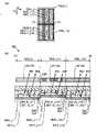
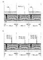
図1(A)および図1(B)はそれぞれ、本発明の一態様の表示パネルの画素と副画素を説明する上面図および断面図である。図1(A)は本発明の一態様の表示パネルの画素の上面図であり、図1(B)は図1(A)の切断線Y3-Y4における断面図である。FIGS. 1A and 1B are a top view and a cross-sectional view, respectively, illustrating a pixel and a subpixel of a display panel of one embodiment of the present invention. FIG. 1A is a top view of a pixel of a display panel of one embodiment of the present invention, and FIG. 1B is a cross-sectional view taken along line Y3-Y4 in FIG. 1A.
図2(A)および図2(B)はそれぞれ、本発明の一態様の表示パネルの画素と副画素を説明する上面図および断面図である。図2(A)は本発明の一態様の表示パネルの画素の上面図であり、図2(B)は図2(A)の切断線Y3-Y4における断面図である。2A and 2B are a top view and a cross-sectional view, respectively, illustrating a pixel and a subpixel of a display panel of one embodiment of the present invention. FIG. 2A is a top view of a pixel of a display panel of one embodiment of the present invention, and FIG. 2B is a cross-sectional view taken along line Y3-Y4 in FIG. 2A.
図3は本発明の一態様の表示パネルの構成を説明する図である。図3(A)は表示パネルの上面図であり、図3(B)は図3(A)に示す表示パネルの画素の一部を説明する上面図である。図3(C)は図3(A)に示す表示パネルの断面の構成を説明する模式図である。FIG. 3 illustrates a structure of a display panel of one embodiment of the present invention. FIG. 3A is a top view of a display panel, and FIG. 3B is a top view illustrating part of a pixel of the display panel shown in FIG. 3A. FIG. 3C is a schematic diagram illustrating a cross-sectional structure of the display panel shown in FIG. 3A.
図6は図3(A)に示す表示パネルの画素の構成を説明する上面図である。FIG. 6 is a top view illustrating the structure of a pixel of the display panel shown in FIG. 3A.
図4および図5は表示パネルの構成を説明する断面図である。図4(A)は図3(A)の切断線X1-X2、切断線X3-X4、図6の切断線X5-X6における断面図であり、図4(B)および図4(C)はいずれも図4(A)の一部を説明する図である。4 and 5 are sectional views for explaining the configuration of the display panel. FIG. 4A is a cross-sectional view taken along section lines X1-X2, X3-X4, and X5-X6 in FIG. 3A, and FIGS. All of them are diagrams for explaining a part of FIG. 4(A).
図5は図6の切断線X7-X8、図3(A)の切断線X9-X10における断面図である。5 is a cross-sectional view taken along line X7-X8 in FIG. 6 and line X9-X10 in FIG. 3A.
図7は本発明の一態様の表示パネルが備える画素回路の構成を説明する回路図である。FIG. 7 is a circuit diagram illustrating the structure of a pixel circuit included in the display panel of one embodiment of the present invention.
なお、本明細書において、1以上の整数を値にとる変数を符号に用いる場合がある。例えば、1以上の整数の値をとる変数pを含む(p)を、最大p個の構成要素のいずれかを特定する符号の一部に用いる場合がある。また、例えば、1以上の整数の値をとる変数mおよび変数nを含む(m,n)を、最大m×n個の構成要素のいずれかを特定する符号の一部に用いる場合がある。In this specification, a variable whose value is an integer of 1 or more may be used as a code. For example, (p), which includes a variable p that takes an integer value of 1 or more, may be used as part of the code specifying one of the maximum p components. Also, for example, (m, n) including variable m and variable n, which take integer values of 1 or more, may be used as part of the code specifying one of the maximum m×n components.
<表示パネルの構成例1>
本実施の形態で説明する表示パネル700は、複数の画素を備える。当該複数の画素は、色相が互いに異なる色を表示する機能を備える。<Configuration example 1 of display panel>
The
当該複数の画素を用いて、各々その画素では表示できない色相の色を、加法混色により表示することができる。By using the plurality of pixels, colors of hues that cannot be displayed by the pixels can be displayed by additive color mixture.
なお、色相が異なる色を表示することができる複数の画素を混色に用いる場合において、それぞれの画素を副画素と言い換えることができる。また、複数の副画素を一組にして、画素と言い換えることができる。Note that when a plurality of pixels capable of displaying colors with different hues are used for color mixture, each pixel can be called a sub-pixel. Also, a set of sub-pixels can be called a pixel.
例えば、画素702(i,j)、画素702(i,j+1)および画素702(i,j+2)を、いずれも副画素とみなし、これらを一組にして画素703(i,k)と言い換えることができる(図1(A)参照)。For example, pixel 702(i,j), pixel 702(i,j+1), and pixel 702(i,j+2) are all considered sub-pixels and grouped together as pixel 703(i,k). (See FIG. 1(A)).
具体的には、赤色を表示する画素702(i,j)、緑色を表示する画素702(i,j+1)および青色を表示する画素702(i,j+2)を副画素とみなし、一組にして、画素703(i,k)に用いることができる。Specifically, a pixel 702 (i, j) displaying red, a pixel 702 (i, j+1) displaying green, and a pixel 702 (i, j+2) displaying blue are regarded as sub-pixels, and , can be used for pixel 703(i,k).
また、例えば、白色を表示する副画素等を上記の一組に加えて、画素に用いることができる。Further, for example, a sub-pixel or the like that displays white can be added to the above set and used as a pixel.
<表示素子の構成例1>
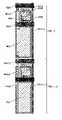
画素702(i,j)は、表示素子550(i,j)を有する(図1(B)参照)。表示素子550(i,j)は、光を射出する機能を備える。例えば、有機EL素子を表示素子550(i,j)に用いることができる。表示素子550(i,j)は発光層553、電極551(i,j)、電極552を備える。例えば、電極551(i,j)は光透過性を有する材料、電極552は光反射性を有する材料を用いる。画素702(i,j+1)および画素702(i,j+2)についても同様である。発光層553は、発光性の材料を含む層である。<Configuration example 1 of display element>
A pixel 702(i,j) has a display element 550(i,j) (see FIG. 1B). The display element 550(i, j) has a function of emitting light. For example, an organic EL element can be used for the display element 550(i,j). A display element 550 (i, j) includes a light-emitting
また後述の部分で説明するが、画素702(i,j)は赤色の着色膜CF1(R)を備え、画素702(i,j+1)は緑色の着色膜CF1(G)を備え、画素702(i,j+2)は青色の着色膜CF1(B)を備える。As will be described later, the pixel 702(i, j) has a red colored film CF1(R), the pixel 702(i, j+1) has a green colored film CF1(G), and the pixel 702( i, j+2) is provided with a blue colored film CF1(B).
表示素子550(i,j)において、半光透過性・半光反射性を備える導電膜551_0(i,j)と、光透過性を備える導電膜551_1(i,j)とを、電極551(i,j)に用いることができる。表示素子550(i,j+1)、表示素子550(i,j+2)においても同様である。In the display element 550 (i, j), a semi-transmissive/semi-reflective conductive film 551_0 (i, j) and a light-transmitting conductive film 551_1 (i, j) are connected to electrodes 551 (i, j). i, j). The same applies to display element 550 (i, j+1) and display element 550 (i, j+2).
光透過性を備える導電膜551_1(i,j)は、半光透過性・半光反射性を備える導電膜551_0(i,j)および発光層553の間に挟まれる領域を備える。The light-transmitting conductive film 551_1(i, j) includes a region sandwiched between the semi-light-transmitting/semi-reflecting conductive film 551_0(i, j) and the light-emitting
この場合において、発光層553と、光透過性を備える導電膜551_1(i,j)との積層膜を、光透過性を有する膜とみなすことができる。表示素子550(i,j+1)、表示素子550(i,j+2)においても同様である。In this case, a stacked film of the light-emitting
画素702(i,j)、画素702(i,j+1)、画素702(i,j+2)は微少共振器構造を備える。微小光共振器構造とは、光透過性を有し、厚さ方向において所定の光学距離を有する膜を、半光透過性・半光反射性を備える膜と、光反射膜との間に挟む積層構造を指す。光透過性を有する導電膜551_1(i,j)は、光透過率の異なる2種以上の積層構造としても良い。Pixel 702(i,j), pixel 702(i,j+1), and pixel 702(i,j+2) have a microresonator structure. An optical microresonator structure is one in which a film having optical transparency and a predetermined optical distance in the thickness direction is sandwiched between a semi-optical transmissive/semi-reflective film and a light-reflecting film. Refers to a laminated structure. The light-transmitting conductive film 551_1(i, j) may have a layered structure of two or more layers with different light transmittances.
図1(B)には、赤色の光R01及びR02、緑色の光G01及びG02、青色の光B01及びB02が示されている。いずれの光も発光層553から射出される。また、d0、d1が示されている。d0、d1はいずれも、導電膜551_0(i,j)と電極552との間の、導電膜551_0の膜厚方向に沿った距離である。FIG. 1B shows red lights R01 and R02, green lights G01 and G02, and blue lights B01 and B02. Both lights are emitted from the
光R02、光G02、光B02、は半光透過性・半光反射性を備える導電膜551_0(i,j)と、光透過性を備える導電膜551_1(i,j)との界面で反射する。また光R02、光G02、光B02、は発光層553と、光反射性を有する電極552との界面で反射する。Light R02, light G02, and light B02 are reflected at the interface between the conductive film 551_0 (i, j) having semi-light transmissive/semi-light reflective properties and the conductive film 551_1 (i, j) having light transmissive property. . Further, the light R02, the light G02, and the light B02 are reflected at the interface between the light emitting
画素702(i,j)において光R01と光R02とは干渉して強めあう。画素702(i,j+1)において光G01と光G02とは干渉して強めあう。画素702(i,j+2)において光B01と光B02とは干渉して強めあう。At pixel 702(i,j), light R01 and light R02 interfere and strengthen each other. At pixel 702 (i, j+1), light G01 and light G02 interfere and strengthen each other. At pixel 702 (i, j+2), light B01 and light B02 interfere and strengthen each other.
本発明の一態様の表示パネル700において、画素702(i,j)と、画素702(i,j+2)と、は距離d0を有する。また、画素702(i,j)における距離d0と、画素702(i,j+1)における距離d1とは異なる。換言すると、画素702(i,j)における電極552と導電膜551_0(i,j)との距離と、画素702(i,j+2)における電極552と導電膜551_0(i,j+2)との距離とは、概略等しい。また、画素702(i,j)における電極552と導電膜551_0(i,j)との距離と、画素702(i,j+1)における電極552と導電膜551_0(i,j+1)との距離とは、異なる。なお、本明細書等において、2つの距離が概略等しいとは、2つの距離のうちの一方の、他方に対する比が0.8以上1.2以下であることを示す。In the
光透過性を備える導電膜551_1(i,j)の屈折率に波長依存性があり、赤色の光と青色の光とで互いに屈折率が異なるのであれば、画素702(i,j)における距離d0と、画素702(i,j+2)における距離d0とにおいて、光学距離は異なる。表示パネル700において、上記屈折率を考慮して、距離d0を決定することで、有効な微小光共振器構造が形成される。If the refractive index of the conductive film 551_1 (i, j) having optical transparency has wavelength dependence, and red light and blue light have different refractive indices, then the distance in the pixel 702 (i, j) is The optical distance is different between d0 and the distance d0 at pixel 702(i,j+2). In the
なお、半光透過性・半光反射性を備える膜は、可視光の一部を透過する機能および他の一部を反射する機能を備える。具体的には、光が透過する程度に薄い金属膜を半光透過性・半光反射性を備える膜に用いることができる。A semi-transmissive/semi-reflective film has a function of transmitting a part of visible light and a function of reflecting the other part. Specifically, a metal film thin enough to transmit light can be used as a semi-light-transmitting/semi-reflecting film.
これにより、微小光共振器構造を画素702(i,j)、画素702(i,j+1)、画素702(i,j+2)に設けることができる。画素702(i,j)は、赤色の色純度を高め、表示を鮮やかにすることができる。また画素702(i,j+1)は、緑色の色純度を高め、表示を鮮やかにすることができる。また画素702(i,j+2)は、青色の色純度を高め、表示を鮮やかにすることができる。Thereby, a micro optical resonator structure can be provided in pixel 702(i,j), pixel 702(i,j+1), and pixel 702(i,j+2). Pixel 702(i,j) can increase the color purity of red and make the display more vivid. Also, the pixel 702 (i, j+1) can increase the color purity of green and make the display vivid. In addition, the pixel 702 (i, j+2) can increase the color purity of blue to make the display more vivid.
または、所定の波長の光を他の光より効率よく取り出すことができる。または、スペクトルの半値幅が狭い光を取り出すことができる。または、鮮やかな色の光を取り出すことができる。Alternatively, light with a predetermined wavelength can be extracted more efficiently than other light. Alternatively, light with a narrow half width of the spectrum can be extracted. Or you can take out bright colors of light.
また表示パネル700_1のように、導電膜551_1(i,j)に接して導電膜551_2(i,j)を設ける積層構造としてもよい(図2(B)参照)。ここで、導電膜551_1(i,j)と、導電膜551_2(i,j)とは異なる材料であると好ましい。なお、導電膜551_1(i,j)と、導電膜551_2(i,j)は同じ材料としてもよい。導電膜551_1(i,j+2)においても同様である。Alternatively, a stacked structure in which a conductive film 551_2(i, j) is provided in contact with the conductive film 551_1(i, j) may be employed like the display panel 700_1 (see FIG. 2B). Here, it is preferable that the conductive films 551_1(i, j) and the conductive films 551_2(i, j) are made of different materials. Note that the conductive film 551_1(i, j) and the conductive film 551_2(i, j) may be made of the same material. The same applies to the conductive film 551_1(i, j+2).
表示素子550(i,j)において、半光透過性・半光反射性を備える導電膜551_0(i,j)と、光透過性を備える導電膜551_1(i,j)と、光透過性を備える導電膜551_2(i,j)とを、電極551(i,j)に用いることができる。表示素子550(i,j+2)においても同様である。In the display element 550(i, j), a conductive film 551_0(i, j) having semi-transmissive/semi-light reflective properties, a conductive film 551_1(i, j) having light-transmitting properties, and a conductive film 551_1(i, j) having light-transmitting properties The conductive film 551_2(i,j) provided can be used for the electrode 551(i,j). The same applies to display element 550 (i, j+2).
光透過性を備える導電膜551_1(i,j)は、半光透過性・半光反射性を備える導電膜551_0(i,j)および発光層553の間に挟まれる領域を備える。また、光透過性を備える導電膜551_2(i,j)は、光透過性を備える導電膜551_1(i,j)および発光層553の間に挟まれる領域を備える。この場合において、発光層553、光透過性を備える導電膜551_1(i,j)および光透過性を備える導電膜551_2(i,j)の積層膜を光透過性を有する膜とみなすことができる。表示素子550(i,j+2)においても同様である。The light-transmitting conductive film 551_1(i, j) has a region sandwiched between the semi-light-transmitting/semi-reflecting conductive film 551_0(i, j) and the light-emitting
表示素子550(i,j+1)において、半光透過性・半光反射性を備える導電膜551_0(i,j+1)と、光透過性を備える導電膜551_1(i,j+1)とを、電極551(i,j+1)に用いることができる。In the display element 550 (i, j+1), a semi-transmissive/semi-reflective conductive film 551_0 (i, j+1) and a light-transmitting conductive film 551_1 (i, j+1) are connected to the electrode 551 ( i, j+1).
光透過性を備える導電膜551_1(i,j+1)は、半光透過性・半光反射性を備える導電膜551_0(i,j+1)および発光層553の間に挟まれる領域を備える。この場合において、発光層553および光透過性を備える導電膜551_1(i,j+1)の積層膜を光透過性を有する膜とみなすことができる。The light-transmitting conductive film 551_1 (i, j+1) has a region sandwiched between the semi-light-transmitting/semi-light-reflecting conductive film 551_0 (i, j+1) and the light-emitting
実施の形態2で説明するが、電極551(i,j)が、表示パネル700_1のような、積層構造を有する場合、電極551(i,j)の作製工程の簡略化に有効である。As described in
<画素の構成例1>
例えば、白色の光を発する発光層を発光層553に用いることができる(図2(B)参照)。<Pixel configuration example 1>
For example, a light-emitting layer that emits white light can be used for the light-emitting layer 553 (see FIG. 2B).
画素702(i,j)は赤色の着色膜CF1(R)を備え、赤色の光を射出する機能を備える(図2(B)参照)。画素702(i,j+1)は緑色の着色膜CF1(G)を備え、緑色の光を射出する機能を備える。画素702(i,j+2)は青色の着色膜CF1(B)を備え、青色の光を射出する機能を備える。副画素は、互いに絶縁膜528で区切られている。発光層553は、画素702(i,j)において配設される領域、画素702(i,j+1)において配設される領域、画素702(i,j+2)において配設される領域、を有する。A pixel 702(i, j) includes a red colored film CF1(R) and has a function of emitting red light (see FIG. 2B). The pixel 702(i, j+1) has a green colored film CF1(G) and has a function of emitting green light. A pixel 702 (i, j+2) includes a blue colored film CF1 (B) and has a function of emitting blue light. Sub-pixels are separated from each other by an insulating
画素702(i,j)において、発光層553は、例えば188nmの膜厚とすることができる。導電膜551_1(i,j)は、例えば膜厚50nmの、インジウムと錫と珪素とを有する酸化物導電膜を用いることができる。導電膜551_2(i,j)は、例えば膜厚62nmの、インジウムと亜鉛とを有する酸化物導電膜を用いることができる。画素702(i,j+2)においても同様である。In pixel 702(i,j), light-emitting
画素702(i,j+1)において、発光層553は、例えば188nmの膜厚とすることができる。導電膜551_1(i,j+1)は、例えば膜厚50nmの、インジウムと錫と珪素とを有する酸化物導電膜を用いることができる。In pixel 702(i,j+1), the light-emitting
上記膜厚による各副画素の構成により、画素702(i,j)は赤色の色純度を高め、画素702(i,j+1)は緑色の色純度を高め、画素702(i,j+1)は青色の色純度を高め、いずれの表示も鮮やかにすることができる。By configuring each sub-pixel with the above film thickness, the pixel 702(i,j) enhances the color purity of red, the pixel 702(i,j+1) enhances the color purity of green, and the pixel 702(i,j+1) enhances the color purity of blue. The color purity of the display can be increased, and any display can be made vivid.
<表示パネルの構成例2>
本実施の形態で説明する表示パネル700は、画素702(i,j)を有する(図3(A)または図17参照)。<Configuration example 2 of the display panel>
A
<画素の構成例2>
画素702(i,j)は、表示素子550(i,j)を備える(図3(C)参照)。また、画素702(i,j)は、画素回路530(i,j)を備える。<Example 2 of Pixel Configuration>
A pixel 702(i,j) includes a display element 550(i,j) (see FIG. 3C). Pixel 702(i,j) also includes pixel circuit 530(i,j).
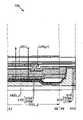
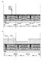
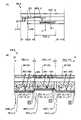
画素回路530(i,j)は導電膜を備える。当該導電膜は可視光を透過する領域を備えてもよい。例えば、可視光を透過する導電膜を導電膜512A、導電膜512Bおよび導電膜504に用いることができる(図4(A)参照)。The pixel circuit 530(i,j) comprises a conductive film. The conductive film may have a region that transmits visible light. For example, a conductive film that transmits visible light can be used for the
なお、導電膜512A、導電膜512Bおよび導電膜504は、いずれもトランジスタMの電極の機能を備える。または、導電膜512A、導電膜512Bおよび導電膜504は、いずれも画素回路530(i,j)の配線の機能を備える(図4(A)または図4(B)参照)。Note that the
<表示素子の構成例2>
表示素子550(i,j)は画素回路530(i,j)と電気的に接続される(図3(C)参照)。例えば、表示素子550(i,j)は、接続部522Aにおいて、画素回路530(i,j)と電気的に接続される。具体的には、表示素子550(i,j)の電極551(i,j)は、トランジスタMの導電膜512Aと電気的に接続される。<Configuration Example 2 of Display Element>
The display element 550(i, j) is electrically connected to the pixel circuit 530(i, j) (see FIG. 3C). For example, display element 550(i,j) is electrically connected to pixel circuit 530(i,j) at
表示素子550(i,j)は、基板770に向かって可視光を射出する機能を備える(図3(C)、図4(A)参照)。このとき光L1の射出する経路に、着色膜CF1(R)を設けることができる。表示素子550(i,j+1)、表示素子550(i,j+2)も同様とする。The display element 550(i, j) has a function of emitting visible light toward the substrate 770 (see FIGS. 3C and 4A). At this time, a colored film CF1(R) can be provided on the path through which the light L1 is emitted. The same applies to display element 550 (i, j+1) and display element 550 (i, j+2).
<画素回路の構成例1>
画素回路530(i,j)は、トランジスタMを備え、トランジスタMは、半導体膜508、導電膜512A、導電膜512Bおよびゲート電極として機能する導電膜504を備える。<Configuration Example 1 of Pixel Circuit>
The pixel circuit 530(i,j) includes a transistor M, which includes a
半導体膜508は、導電膜512Aと電気的に接続される領域508A、導電膜512Bと電気的に接続される領域508Bを備える(図4(B)参照)。The
半導体膜508は、領域508Aおよび領域508Bの間にゲート電極として機能する導電膜504と重なる領域508Cを備える。The
画素回路530(i,j)は表示素子550(i,j)を駆動する機能を備える(図7参照)。The pixel circuit 530(i,j) has a function of driving the display element 550(i,j) (see FIG. 7).
スイッチ、トランジスタ、ダイオード、抵抗素子、インダクタまたは容量素子等を画素回路530(i,j)に用いることができる。A switch, a transistor, a diode, a resistive element, an inductor, a capacitive element, or the like can be used for the pixel circuit 530(i,j).
例えば、単数または複数のトランジスタをスイッチに用いることができる。または、並列に接続された複数のトランジスタ、直列に接続された複数のトランジスタ、直列と並列が組み合わされて接続された複数のトランジスタを、一のスイッチに用いることができる。For example, one or more transistors can be used for the switches. Alternatively, a plurality of transistors connected in parallel, a plurality of transistors connected in series, or a plurality of transistors connected in series and in parallel can be used for one switch.
例えば、画素回路530(i,j)は、信号線S2(j)、走査線G2(i)および導電膜ANOと電気的に接続される(図7参照)。なお、導電膜512Bは、接続部522Bにおいて導電膜ANOと電気的に接続される(図4(A)および図7参照)。For example, the pixel circuit 530(i,j) is electrically connected to the signal line S2(j), the scanning line G2(i) and the conductive film ANO (see FIG. 7). Note that the
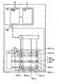
画素回路530(i,j)は、スイッチSW2、トランジスタMおよび容量素子C21を含む(図7参照)。The pixel circuit 530(i,j) includes a switch SW2, a transistor M and a capacitive element C21 (see FIG. 7).
例えば、走査線G2(i)と電気的に接続されるゲート電極と、信号線S2(j)と電気的に接続される第1の電極と、を有するトランジスタを、スイッチSW2に用いることができる。For example, a transistor having a gate electrode electrically connected to the scan line G2(i) and a first electrode electrically connected to the signal line S2(j) can be used for the switch SW2. .
トランジスタMは、スイッチSW2に用いるトランジスタの第2の電極と電気的に接続されるゲート電極と、導電膜ANOと電気的に接続される第1の電極と、を有する。The transistor M has a gate electrode electrically connected to the second electrode of the transistor used for the switch SW2, and a first electrode electrically connected to the conductive film ANO.
なお、半導体膜をゲート電極との間に挟むように設けられた導電膜を備えるトランジスタを、トランジスタMに用いることができる。例えば、トランジスタMのゲート電極と同じ電位を供給することができる配線と電気的に接続される導電膜を当該導電膜に用いることができる。Note that a transistor including a conductive film in which a semiconductor film is interposed with a gate electrode can be used as the transistor M. For example, a conductive film that is electrically connected to a wiring capable of supplying the same potential as that of the gate electrode of the transistor M can be used as the conductive film.
容量素子C21は、スイッチSW2に用いるトランジスタの第2の電極と電気的に接続される第1の電極と、トランジスタMの第1の電極と電気的に接続される第2の電極と、を有する。The capacitive element C21 has a first electrode electrically connected to the second electrode of the transistor used for the switch SW2 and a second electrode electrically connected to the first electrode of the transistor M. .
また、表示素子550(i,j)の電極551(i,j)をトランジスタMの第2の電極と電気的に接続し、表示素子550(i,j)の電極552を導電膜VCOM2と電気的に接続する。これにより、表示素子550(i,j)を駆動することができる。Further, the electrode 551(i,j) of the display element 550(i,j) is electrically connected to the second electrode of the transistor M, and the
<画素の構成例3>
画素702(i,j)は絶縁膜573を備える(図5参照)。例えば、単数の膜または複数の膜を積層した積層膜を絶縁膜573に用いることができる。具体的には、絶縁膜573Aおよび絶縁膜573Bを積層した積層膜を絶縁膜573に用いることができる。<Example 3 of Pixel Configuration>
The pixel 702(i,j) has an insulating film 573 (see FIG. 5). For example, a single film or a stacked film in which a plurality of films are stacked can be used as the insulating
画素702(i,j)は、絶縁膜518を備える。なお、絶縁膜573は、例えば、表示領域231の外側で絶縁膜518と接する領域を備える。The pixel 702 (i,j) comprises an insulating
表示素子550(i,j)は絶縁膜573および絶縁膜518に挟まれる領域を備える。The display element 550 (i, j) has a region sandwiched between the insulating
表示素子550(i,j)は電極551(i,j)、発光層553、および電極552を備える。発光層553は、電極551(i,j)および電極552の間に挟まれる領域を備える。発光層553は、有機化合物を含む。The display element 550(i,j) comprises an electrode 551(i,j), a
これにより、表示素子への不純物の拡散を抑制することができる。その結果、利便性または信頼性に優れた新規な表示装置を提供することができる。This can suppress the diffusion of impurities into the display element. As a result, it is possible to provide a novel display device with excellent convenience or reliability.
<表示パネルの構成例3>
また、本実施の形態で説明する表示パネル700は、表示領域231を有する(図17参照)。<Configuration example 3 of the display panel>
Further, the
<表示領域の構成例>
表示領域231は、一群の複数の画素702(i,1)乃至画素702(i,n)と、他の一群の複数の画素702(1,j)乃至画素702(m,j)と、走査線G2(i)と、信号線S2(j)と、を有する(図17参照)。また、導電膜VCOM2と、導電膜ANOと、を有する。なお、iは1以上m以下の整数であり、jは1以上n以下の整数であり、mおよびnは1以上の整数である。<Configuration example of display area>
The
一群の複数の画素702(i,1)乃至画素702(i,n)は画素702(i,j)を含み、一群の複数の画素702(i,1)乃至画素702(i,n)は行方向(図中に矢印R1で示す方向)に配設される。The group of pixels 702(i,1) through 702(i,n) includes pixel 702(i,j), and the group of pixels 702(i,1) through 702(i,n) includes They are arranged in the row direction (the direction indicated by arrow R1 in the figure).
他の一群の複数の画素702(1,j)乃至画素702(m,j)は画素702(i,j)を含み、他の一群の複数の画素702(1,j)乃至画素702(m,j)は行方向と交差する列方向(図中に矢印C1で示す方向)に配設される。Another group of pixels 702(1,j) through 702(m,j) includes pixel 702(i,j), and another group of pixels 702(1,j) through 702(m) includes pixel 702(i,j). , j) are arranged in the column direction (the direction indicated by arrow C1 in the figure) intersecting the row direction.
走査線G2(i)は、行方向に配設される一群の複数の画素702(i,1)乃至画素702(i,n)と電気的に接続される。The scanning line G2(i) is electrically connected to a group of pixels 702(i,1) to 702(i,n) arranged in the row direction.
信号線S2(j)は、列方向に配設される他の一群の複数の画素702(1,j)乃至画素702(m,j)と電気的に接続される。The signal line S2(j) is electrically connected to another group of pixels 702(1,j) to 702(m,j) arranged in the column direction.
<表示パネルの構成例4>
また、本実施の形態で説明する表示パネル700は、駆動回路GDまたは駆動回路SDを備えることができる(図3(A)および図17参照)。<Display panel configuration example 4>
Further, the
<駆動回路GD>
駆動回路GDは、制御情報に基づいて選択信号を供給する機能を有する。<Drive circuit GD>
The drive circuit GD has a function of supplying a selection signal based on control information.
一例を挙げれば、制御情報に基づいて、30Hz以上、好ましくは60Hz以上の頻度で一の走査線に選択信号を供給する機能を備える。これにより、動画像をなめらかに表示することができる。For example, it has a function of supplying a selection signal to one scanning line at a frequency of 30 Hz or more, preferably 60 Hz or more, based on control information. As a result, moving images can be displayed smoothly.
例えば、制御情報に基づいて、30Hz未満、好ましくは1Hz未満より好ましくは一分に一回未満の頻度で一の走査線に選択信号を供給する機能を備える。これにより、フリッカーが抑制された状態で静止画像を表示することができる。For example, based on the control information, it provides a selection signal to one scan line at a frequency of less than 30 Hz, preferably less than 1 Hz, and more preferably less than once per minute. As a result, a still image can be displayed with flicker suppressed.
また、表示パネルは、複数の駆動回路を有することができる。例えば、表示パネル700Bは、駆動回路GDAおよび駆動回路GDBを有する(図18参照)。Also, the display panel can have a plurality of drive circuits. For example, the
また、例えば、複数の駆動回路を備える場合、駆動回路GDAが選択信号を供給する頻度と、駆動回路GDBが選択信号を供給する頻度とを、異ならせることができる。具体的には、静止画像を表示する一の領域に選択信号を供給する頻度より高い頻度で、動画像を表示する他の領域に選択信号を供給することができる。これにより、一の領域にフリッカーが抑制された状態で静止画像を表示し、他の領域に滑らかに動画像を表示することができる。Further, for example, when a plurality of driving circuits are provided, the frequency of supplying the selection signal by the driving circuit GDA and the frequency of supplying the selection signal by the driving circuit GDB can be made different. Specifically, the selection signal can be supplied to the other area displaying the moving image at a frequency higher than the frequency of supplying the selection signal to one area displaying the still image. As a result, a still image can be displayed in one area with flicker suppressed, and a moving image can be smoothly displayed in another area.
<駆動回路SD>
駆動回路SDは、駆動回路SD1と、駆動回路SD2と、を有する。駆動回路SD1は、情報V11に基づいて画像信号を供給する機能を有し、駆動回路SD2は、情報V12に基づいて画像信号を供給する機能を有する(図22または図23参照)。<Drive circuit SD>
The drive circuit SD has a drive circuit SD1 and a drive circuit SD2. The drive circuit SD1 has a function of supplying an image signal based on the information V11, and the drive circuit SD2 has a function of supplying an image signal based on the information V12 (see FIG. 22 or 23).
駆動回路SD1または駆動回路SD2は、画像信号を生成する機能と、当該画像信号を一の表示素子と電気的に接続される画素回路に供給する機能を備える。具体的には、極性が反転する信号を生成する機能を備える。これにより、例えば、液晶表示素子を駆動することができる。The drive circuit SD1 or the drive circuit SD2 has a function of generating an image signal and a function of supplying the image signal to a pixel circuit electrically connected to one display element. Specifically, it has a function of generating a signal whose polarity is inverted. Thereby, for example, a liquid crystal display element can be driven.
例えば、シフトレジスタ等のさまざまな順序回路等を駆動回路SDに用いることができる。For example, various sequential circuits such as shift registers can be used for the drive circuit SD.
例えば、駆動回路SD1および駆動回路SD2が集積された集積回路を、駆動回路SDに用いることができる。具体的には、シリコン基板上に形成された集積回路を駆動回路SDに用いることができる。For example, an integrated circuit in which the drive circuit SD1 and the drive circuit SD2 are integrated can be used as the drive circuit SD. Specifically, an integrated circuit formed on a silicon substrate can be used for the drive circuit SD.
例えば、COG(Chip on glass)法またはCOF(Chip on Film)法を用いて、集積回路を端子に実装することができる。具体的には、異方性導電膜を用いて、集積回路を端子に実装することができる。For example, the COG (Chip on glass) method or the COF (Chip on Film) method can be used to mount the integrated circuit on the terminals. Specifically, an anisotropic conductive film can be used to mount an integrated circuit on the terminals.
<表示パネルの構成例5>
また、本実施の形態で説明する表示パネル700は、端子519B、基板570、基板770、接合層505、機能膜770P等を備える(図4(A)または図5参照)。<Display panel configuration example 5>
In addition, the
<端子519B>
端子519Bは、例えば、導電膜511Bを備える。端子519Bは、例えば、信号線S2(j)と電気的に接続することができる。<
The terminal 519B includes, for example, a
<基板570、基板770>
基板770は、基板570と重なる領域を備える。基板770は、基板570との間に表示素子550(i,j)を挟む領域を備える。<
基板770の、表示素子550(i,j)と重なる領域において、例えば、複屈折が抑制された材料を用いることができる。A material with reduced birefringence, for example, can be used in a region of the
<接合層505>
接合層505は、基板770および基板570を貼り合せる機能を備える。<Joining
The
<機能膜770P等>
機能膜770Pは、表示素子550(i,j)と重なる領域を備える。<
The
<構成要素の例>
表示パネル700は、基板570、基板770または接合層505を有する。<Examples of components>
The
また、表示パネル700は、絶縁膜521A、絶縁膜521B、絶縁膜528、絶縁膜516、絶縁膜503または絶縁膜506を有する。The
また、表示パネル700は、信号線S2(j)、走査線G2(i)または導電膜ANOを有する。The
また、表示パネル700は、端子519Bまたは導電膜511Bを有する。The
また、表示パネル700は、画素回路530(i,j)またはトランジスタMを有する。The
また、表示パネル700は、表示素子550(i,j)、電極551(i,j)、電極552または発光層553(j)を有する。The
また、表示パネル700は、絶縁膜573を有する。The
また、表示パネル700は、駆動回路GDまたは駆動回路SDを有する。In addition, the
<基板570>
作製工程中の熱処理に耐えうる程度の耐熱性を有する材料を基板570に用いることができる。<
A material having heat resistance enough to withstand heat treatment during the manufacturing process can be used for the
例えば、厚さ0.7mm以下厚さ0.1mm以上の材料を基板570に用いることができる。具体的には、厚さ0.1mm程度まで研磨又はエッチングした材料を用いることができる。For example, a material having a thickness of 0.7 mm or less and 0.1 mm or more can be used for the
例えば、第6世代(1500mm×1850mm)、第7世代(1870mm×2200mm)、第8世代(2200mm×2400mm)、第9世代(2400mm×2800mm)、第10世代(2950mm×3400mm)等の面積が大きなガラス基板を基板570に用いることができる。これにより、大型の表示装置を作製することができる。For example, the area of the 6th generation (1500mm x 1850mm), the 7th generation (1870mm x 2200mm), the 8th generation (2200mm x 2400mm), the 9th generation (2400mm x 2800mm), the 10th generation (2950mm x 3400mm), etc. A large glass substrate can be used for
有機材料、無機材料または有機材料と無機材料等の複合材料等を基板570に用いることができる。例えば、ガラス、セラミックス、金属等の無機材料を基板570に用いることができる。An organic material, an inorganic material, a composite material of an organic material and an inorganic material, or the like can be used for the
具体的には、無アルカリガラス、ソーダ石灰ガラス、カリガラス、クリスタルガラス、アルミノ珪酸ガラス、強化ガラス、化学強化ガラス、石英またはサファイア等を、基板570に用いることができる。具体的には、無機酸化物膜、無機窒化物膜または無機酸窒化物膜等を、基板570に用いることができる。例えば、酸化シリコン膜、窒化シリコン膜、酸化窒化シリコン膜、酸化アルミニウム膜等を、基板570に用いることができる。ステンレス・スチールまたはアルミニウム等を、基板570に用いることができる。Specifically, alkali-free glass, soda lime glass, potash glass, crystal glass, aluminosilicate glass, tempered glass, chemically tempered glass, quartz, sapphire, or the like can be used for the
例えば、シリコンや炭化シリコンからなる単結晶半導体基板、多結晶半導体基板、シリコンゲルマニウム等の化合物半導体基板、SOI基板等を基板570に用いることができる。これにより、半導体素子を基板570に形成することができる。For example, a single crystal semiconductor substrate made of silicon or silicon carbide, a polycrystalline semiconductor substrate, a compound semiconductor substrate made of silicon germanium or the like, an SOI substrate, or the like can be used as the
例えば、樹脂、樹脂フィルムまたはプラスチック等の有機材料を基板570に用いることができる。具体的には、ポリエステル、ポリオレフィン、ポリアミド、ポリイミド、ポリカーボネートまたはアクリル樹脂等の樹脂フィルムまたは樹脂板を、基板570に用いることができる。For example, an organic material such as resin, resin film, or plastic can be used for
例えば、金属板、薄板状のガラス板または無機材料等の膜を樹脂フィルム等に貼り合わせた複合材料を基板570に用いることができる。例えば、繊維状または粒子状の金属、ガラスもしくは無機材料等を樹脂フィルムに分散した複合材料を、基板570に用いることができる。例えば、繊維状または粒子状の樹脂もしくは有機材料等を無機材料に分散した複合材料を、基板570に用いることができる。For example, the
また、単層の材料または複数の層が積層された材料を、基板570に用いることができる。例えば、基材と基材に含まれる不純物の拡散を防ぐ絶縁膜等が積層された材料を、基板570に用いることができる。具体的には、ガラスとガラスに含まれる不純物の拡散を防ぐ酸化シリコン層、窒化シリコン層または酸化窒化シリコン層等から選ばれた一または複数の膜が積層された材料を、基板570に用いることができる。または、樹脂と樹脂を透過する不純物の拡散を防ぐ酸化シリコン膜、窒化シリコン膜または酸化窒化シリコン膜等が積層された材料を、基板570に用いることができる。Also, a single-layer material or a laminated material of multiple layers can be used for the
具体的には、ポリエステル、ポリオレフィン、ポリアミド、ポリイミド、ポリカーボネート若しくはアクリル樹脂等の樹脂フィルム、樹脂板または積層材料等を基板570に用いることができる。Specifically, the
具体的には、ポリエステル、ポリオレフィン、ポリアミド(ナイロン、アラミド等)、ポリイミド、ポリカーボネート、ポリウレタン、アクリル樹脂、エポキシ樹脂もしくはシリコーン等のシロキサン結合を有する樹脂を含む材料を基板570に用いることができる。Specifically, a material containing a resin having a siloxane bond such as polyester, polyolefin, polyamide (nylon, aramid, etc.), polyimide, polycarbonate, polyurethane, acrylic resin, epoxy resin, or silicone can be used for the
具体的には、ポリエチレンテレフタレート(PET)、ポリエチレンナフタレート(PEN)、ポリエーテルサルフォン(PES)またはアクリル樹脂等を基板570に用いることができる。または、シクロオレフィンポリマー(COP)、シクロオレフィンコポリマー(COC)等を用いることができる。Specifically, polyethylene terephthalate (PET), polyethylene naphthalate (PEN), polyethersulfone (PES), acrylic resin, or the like can be used for the
また、紙または木材などを基板570に用いることができる。Alternatively, paper, wood, or the like can be used for the
例えば、可撓性を有する基板を基板570に用いることができる。For example, a flexible substrate can be used for the
なお、トランジスタまたは容量素子等を基板に直接形成する方法を用いることができる。また、例えば作製工程中に加わる熱に耐熱性を有する工程用の基板にトランジスタまたは容量素子等を形成し、形成されたトランジスタまたは容量素子等を基板570に転置する方法を用いることができる。これにより、例えば可撓性を有する基板にトランジスタまたは容量素子等を形成できる。Note that a method of directly forming a transistor, a capacitor, or the like over a substrate can be used. Alternatively, for example, a method can be used in which a transistor, a capacitor, or the like is formed over a process substrate that is resistant to heat applied during a manufacturing process, and the formed transistor, capacitor, or the like is transferred to the
<基板770>
例えば、基板570に用いることができる材料を基板770に用いることができる。例えば、基板570に用いることができる材料から選択された光透過性を備える材料を、基板770に用いることができる。または、片側の表面に、例えば1μm以下の反射防止膜が形成された材料を基板770に用いることができる。具体的には、誘電体を3層以上、好ましくは5層以上、より好ましくは15層以上積層した積層膜を基板770に用いることができる。これにより、反射率を0.5%以下好ましくは0.08%以下に抑制することができる。<
For example, any material that can be used for
例えば、アルミノ珪酸ガラス、強化ガラス、化学強化ガラスまたはサファイア等を、表示パネルの使用者に近い側に配置される基板770に好適に用いることができる。これにより、使用に伴う表示パネルの破損や傷付きを防止することができる。For example, aluminosilicate glass, tempered glass, chemically tempered glass, sapphire, or the like can be suitably used for the
例えば、樹脂フィルムを基板770に好適に用いることができる。これにより、重量を低減することができる。または、例えば、落下に伴う破損等の発生頻度を低減することができる。For example, a resin film can be suitably used for the
また、例えば、厚さ0.7mm以下厚さ0.1mm以上の材料を基板770に用いることができる。具体的には、厚さを薄くするために研磨した基板を用いることができる。これにより、重量を低減することができる。Further, for example, a material having a thickness of 0.7 mm or less and 0.1 mm or more can be used for the
<絶縁膜521A、絶縁膜521B>
例えば、絶縁性の無機材料、絶縁性の有機材料または無機材料と有機材料を含む絶縁性の複合材料を、絶縁膜521Aまたは絶縁膜521Bに用いることができる。<Insulating
For example, an insulating inorganic material, an insulating organic material, or an insulating composite material containing an inorganic material and an organic material can be used for the insulating
具体的には、無機酸化物膜、無機窒化物膜または無機酸化窒化物膜等またはこれらから選ばれた複数を積層した積層材料を、絶縁膜521Aまたは絶縁膜521Bに用いることができる。Specifically, an inorganic oxide film, an inorganic nitride film, an inorganic oxynitride film, or the like, or a laminated material obtained by laminating a plurality of films selected from these can be used for the insulating
例えば、酸化シリコン膜、窒化シリコン膜、酸化窒化シリコン膜、酸化アルミニウム膜等またはこれらから選ばれた複数を積層した積層材料を含む膜を、絶縁膜521Aまたは絶縁膜521Bに用いることができる。なお、窒化シリコン膜は緻密な膜であり、不純物の拡散を抑制する機能に優れる。For example, a film containing a laminated material in which a silicon oxide film, a silicon nitride film, a silicon oxynitride film, an aluminum oxide film, or a plurality of films selected from these are laminated can be used as the insulating
例えば、ポリエステル、ポリオレフィン、ポリアミド、ポリイミド、ポリカーボネート、ポリシロキサン若しくはアクリル樹脂等またはこれらから選択された複数の樹脂の積層材料もしくは複合材料などを絶縁膜521Aまたは絶縁膜521Bに用いることができる。また、感光性を有する材料を用いて形成してもよい。これにより、絶縁膜521Aまたは絶縁膜521Bは、例えば、絶縁膜521Aまたは絶縁膜521Bと重なるさまざまな構造に由来する段差を平坦化することができる。For example, the insulating
なお、ポリイミドは熱的安定性、絶縁性、靱性、低誘電率、低熱膨張率、耐薬品性などの特性において他の有機材料に比べて優れた特性を備える。これにより、特にポリイミドを絶縁膜521Aまたは絶縁膜521B等に好適に用いることができる。In addition, polyimide is superior to other organic materials in properties such as thermal stability, insulation, toughness, low dielectric constant, low coefficient of thermal expansion, and chemical resistance. Thereby, polyimide can be suitably used for the insulating
例えば、感光性を有する材料を用いて形成された膜を絶縁膜521Aまたは絶縁膜521Bに用いることができる。具体的には、感光性のポリイミドまたは感光性のアクリル樹脂等を用いて形成された膜を絶縁膜521Aまたは絶縁膜521Bに用いることができる。For example, a film formed using a photosensitive material can be used as the insulating
例えば、光透過性を有する材料を絶縁膜521Aまたは絶縁膜521Bに用いることができる。具体的には、窒化シリコンを絶縁膜521Aまたは絶縁膜521Bに用いることができる。For example, a light-transmitting material can be used for the insulating
<絶縁膜528>
例えば、絶縁膜521Aまたは絶縁膜521Bに用いることができる材料を絶縁膜528に用いることができる。具体的には、ポリイミドを含む膜を絶縁膜528に用いることができる。<Insulating
For example, a material that can be used for the insulating
<絶縁膜518>
例えば、絶縁膜521Aまたは絶縁膜521Bに用いることができる材料を絶縁膜518に用いることができる。<Insulating
For example, a material that can be used for the insulating
例えば、酸素、水素、水、アルカリ金属、アルカリ土類金属等の拡散を抑制する機能を備える材料を絶縁膜518に用いることができる。具体的には、窒化物絶縁膜を絶縁膜518に用いることができる。例えば、窒化シリコン、窒化酸化シリコン、窒化アルミニウム、窒化酸化アルミニウム等を絶縁膜518に用いることができる。これにより、トランジスタの半導体膜への不純物の拡散を抑制することができる。例えば、トランジスタの半導体膜に用いる酸化物半導体膜からトランジスタの外部への酸素の拡散を抑制することができる。または、トランジスタの外部から酸化物半導体膜への水素または水等の拡散を抑制することができる。For example, a material having a function of suppressing diffusion of oxygen, hydrogen, water, alkali metal, alkaline earth metal, or the like can be used for the insulating
例えば、水素または窒素を供給する機能を有する材料を絶縁膜518に用いることができる。これにより、絶縁膜518に接する膜に水素または窒素を供給することができる。例えば、酸化物半導体膜に接するように絶縁膜518を形成し、当該酸化物半導体膜に水素または窒素を供給することができる。または、当該酸化物半導体膜に導電性を付与することができる。または、当該酸化物半導体膜を第2のゲート電極に用いることができる。For example, a material having a function of supplying hydrogen or nitrogen can be used for the insulating
<絶縁膜516>
例えば、絶縁膜521Aまたは絶縁膜521Bに用いることができる材料を絶縁膜516に用いることができる。具体的には、作製方法が異なる膜を積層した積層膜を絶縁膜516に用いることができる。<Insulating
For example, a material that can be used for the insulating
例えば、厚さが5nm以上150nm以下、好ましくは5nm以上50nm以下の酸化シリコンまたは酸化窒化シリコン等を含む第1の膜と、厚さが30nm以上500nm以下、好ましくは50nm以上400nm以下の、酸化シリコンまたは酸化窒化シリコン等を含む第2の膜とを積層した積層膜を、絶縁膜516に用いることができる。For example, a first film containing silicon oxide or silicon oxynitride having a thickness of 5 nm to 150 nm, preferably 5 nm to 50 nm, and silicon oxide having a thickness of 30 nm to 500 nm, preferably 50 nm to 400 nm Alternatively, a stacked film in which a second film containing silicon oxynitride or the like is stacked can be used for the insulating
具体的には、ESR測定により観測することができるシリコンのダングリングボンドに由来するg=2.001に現れる信号のスピン密度が3×10¹⁷spins/cm3以下である膜を第1の膜に用いると好ましい。これにより、例えば、トランジスタの半導体膜に用いる酸化物半導体膜を、絶縁膜の形成にともなう損傷から、保護することができる。または、シリコンの欠陥に捉えられる酸素を低減することができる。または、酸素の透過または移動を容易にすることができる。Specifically, a film in which the spin density of a signal appearing at g=2.001 derived from a dangling bond of silicon that can be observed by ESR measurement is 3×10¹⁷ spins/cm3 or less is used as the first film. It is preferable to use Accordingly, for example, an oxide semiconductor film used as a semiconductor film of a transistor can be protected from damage caused by formation of an insulating film. Alternatively, oxygen trapped in silicon defects can be reduced. Alternatively, oxygen permeation or migration can be facilitated.
また、例えば、ESR測定により観測することができるシリコンのダングリングボンドに由来するg=2.001に現れる信号のスピン密度が1.5×10¹⁸spins/cm3未満、さらには1×1018spins/cm3以下である材料を第2の膜に用いると好ましい。Further, for example, the spin density of a signal appearing at g=2.001 derived from a silicon dangling bond that can be observed by ESR measurement is less than 1.5×10¹⁸ spins/cm3 , or even 1×10¹⁸ A material with spins/cm3 or less is preferably used for the second film.
<絶縁膜503>
例えば、絶縁膜521Aまたは絶縁膜521Bに用いることができる材料を絶縁膜503に用いることができる。具体的には、窒化シリコン、窒化酸化シリコン、窒化アルミニウム、窒化酸化アルミニウム、酸化シリコンまたは酸化窒化シリコン等を絶縁膜503に用いることができる。これにより、例えば、トランジスタの半導体膜への不純物の拡散を抑制することができる。<Insulating
For example, a material that can be used for the insulating
<絶縁膜506>
例えば、絶縁膜521Aまたは絶縁膜521Bに用いることができる材料を絶縁膜506に用いることができる。具体的には、酸素の透過を抑制する機能を備える第1の膜と、酸素を供給する機能を備える第2の膜とを積層した積層膜を、絶縁膜506に用いることができる。これにより、例えば、トランジスタの半導体膜に用いる酸化物半導体膜に酸素を拡散することができる。<Insulating
For example, a material that can be used for the insulating
具体的には、酸化シリコン膜、酸化窒化シリコン膜、窒化酸化シリコン膜、窒化シリコン膜、酸化アルミニウム膜、酸化ハフニウム膜、酸化イットリウム膜、酸化ジルコニウム膜、酸化ガリウム膜、酸化タンタル膜、酸化マグネシウム膜、酸化ランタン膜、酸化セリウム膜または酸化ネオジム膜を含む膜を絶縁膜506に用いることができる。Specifically, a silicon oxide film, a silicon oxynitride film, a silicon nitride oxide film, a silicon nitride film, an aluminum oxide film, a hafnium oxide film, an yttrium oxide film, a zirconium oxide film, a gallium oxide film, a tantalum oxide film, and a magnesium oxide film. , a lanthanum oxide film, a cerium oxide film, or a neodymium oxide film can be used as the insulating
例えば、酸素雰囲気下において形成された膜を第2の膜に用いることができる。または、成膜後に酸素を導入した膜を第2の膜に用いることができる。具体的には、イオン注入法、イオンドーピング法、プラズマイマージョンイオン注入法、プラズマ処理等を用いて成膜後に酸素を導入することができる。For example, a film formed in an oxygen atmosphere can be used as the second film. Alternatively, a film into which oxygen is introduced after deposition can be used as the second film. Specifically, oxygen can be introduced after film formation by using an ion implantation method, an ion doping method, a plasma immersion ion implantation method, plasma treatment, or the like.
<絶縁膜573>
例えば、絶縁膜521Aまたは絶縁膜521Bに用いることができる材料を絶縁膜573に用いることができる。具体的には、絶縁膜573Aおよび絶縁膜573Bを積層した積層膜を絶縁膜573に用いることができる。<Insulating
For example, a material that can be used for the insulating
例えば、酸化物または窒化物を絶縁膜573に用いることができる。具体的には、酸化アルミニウム、酸化ガリウム、酸化ゲルマニウム、酸化イットリウム、酸化ジルコニウム、酸化ランタン、酸化ネオジム、酸化ハフニウム、酸化タンタル、窒化シリコンまたは窒化アルミニウム等を絶縁膜573に用いることができる。For example, oxide or nitride can be used for the insulating
具体的には、1×10⁻²g/(m2・day)未満、好ましくは、5×10-3g/(m2・day)以下、好ましくは1×10-4g/(m2・day)以下、好ましくは1×10-5g/(m2・day)以下、好ましくは1×10-6g/(m2・day)以下の水蒸気透過率を備える膜を、絶縁膜573に用いる。Specifically, less than 1×10⁻² g/(m2 ·day), preferably 5×10⁻³ g/(m2 ·day) or less, preferably 1×10⁻⁴ g/(m2 · day) or less, preferably 1 × 10⁻⁵ g/(m2 ·day) or less, preferably 1 × 10⁻⁶ g/(m2 ·day) or less, the insulating
例えば、スパッタリング法を用いて形成することができる膜を絶縁膜573Bに用いることができる。また、原子層堆積法(Atomic Layer Deposition法;ALD法)を用いて形成することができる膜を絶縁膜573Aに用いることができる。これにより、例えば、スパッタリング法を用いて形成される絶縁膜に生じる密度が低い領域を、原子層堆積法を用いて形成される緻密な絶縁膜で覆うことができる。または、スパッタリング法を用いて形成される絶縁膜に生じる不純物が拡散しやすい領域を、原子層堆積法を用いて形成される不純物の拡散しにくい膜で覆うことができる。または、外部から表示素子への不純物の拡散を抑制することができる。For example, a film that can be formed by a sputtering method can be used as the insulating
具体的には、50nm以上1000nm以下、好ましくは100nm以上300nm以下の厚さの酸化アルミニウムを含む膜を、絶縁膜573Bに用いることができる。また、1nm以上100nm以下、好ましくは5nm以上50nm以下の厚さの酸化アルミニウムを含む膜を、絶縁膜573Aに用いることができる。Specifically, a film containing aluminum oxide with a thickness of 50 nm to 1000 nm, preferably 100 nm to 300 nm can be used as the insulating
<配線、端子、導電膜>
導電性を備える材料を配線等に用いることができる。具体的には、導電性を備える材料を、信号線S2(j)、走査線G2(i)、導電膜ANO、端子519Bまたは導電膜511B等に用いることができる。<Wiring, terminal, conductive film>
A material having conductivity can be used for wiring or the like. Specifically, a material having conductivity can be used for the signal line S2(j), the scanning line G2(i), the conductive film ANO, the terminal 519B, the
例えば、無機導電性材料、有機導電性材料、金属または導電性セラミックスなどを配線等に用いることができる。For example, inorganic conductive materials, organic conductive materials, metals, conductive ceramics, or the like can be used for wiring or the like.
具体的には、アルミニウム、金、白金、銀、銅、クロム、タンタル、チタン、モリブデン、タングステン、ニッケル、鉄、コバルト、パラジウムまたはマンガンから選ばれた金属元素などを、配線等に用いることができる。または、上述した金属元素を含む合金などを、配線等に用いることができる。特に、銅とマンガンの合金がウエットエッチング法を用いた微細加工に好適である。Specifically, a metal element selected from aluminum, gold, platinum, silver, copper, chromium, tantalum, titanium, molybdenum, tungsten, nickel, iron, cobalt, palladium, or manganese can be used for wiring or the like. . Alternatively, an alloy or the like containing any of the metal elements described above can be used for wiring or the like. In particular, an alloy of copper and manganese is suitable for fine processing using a wet etching method.
具体的には、アルミニウム膜上にチタン膜を積層する二層構造、窒化チタン膜上にチタン膜を積層する二層構造、窒化チタン膜上にタングステン膜を積層する二層構造、窒化タンタル膜または窒化タングステン膜上にタングステン膜を積層する二層構造、チタン膜と、そのチタン膜上にアルミニウム膜を積層し、さらにその上にチタン膜を形成する三層構造等を配線等に用いることができる。Specifically, a two-layer structure in which a titanium film is stacked over an aluminum film, a two-layer structure in which a titanium film is stacked over a titanium nitride film, a two-layer structure in which a tungsten film is stacked over a titanium nitride film, a tantalum nitride film, or a A two-layer structure in which a tungsten film is laminated on a tungsten nitride film, a three-layer structure in which a titanium film is laminated on the titanium film, an aluminum film is laminated on the titanium film, and a titanium film is further formed thereon can be used for wiring or the like. .
具体的には、酸化インジウム、インジウム錫酸化物、インジウム亜鉛酸化物、酸化亜鉛、ガリウムを添加した酸化亜鉛などの導電性酸化物を、配線等に用いることができる。Specifically, a conductive oxide such as indium oxide, indium tin oxide, indium zinc oxide, zinc oxide, or gallium-added zinc oxide can be used for wiring or the like.
具体的には、グラフェンまたはグラファイトを含む膜を配線等に用いることができる。Specifically, a film containing graphene or graphite can be used for wiring or the like.
例えば、酸化グラフェンを含む膜を形成し、酸化グラフェンを含む膜を還元することにより、グラフェンを含む膜を形成することができる。還元する方法としては、熱を加える方法や還元剤を用いる方法等を挙げることができる。For example, a graphene-containing film can be formed by forming a graphene oxide-containing film and reducing the graphene oxide-containing film. Examples of the reduction method include a method of applying heat and a method of using a reducing agent.
例えば、金属ナノワイヤーを含む膜を配線等に用いることができる。具体的には、銀を含むナノワイヤーを用いることができる。For example, a film containing metal nanowires can be used for wiring or the like. Specifically, nanowires containing silver can be used.
具体的には、導電性高分子を配線等に用いることができる。Specifically, a conductive polymer can be used for wiring and the like.
なお、例えば、導電材料ACF1を用いて、端子519Bとフレキシブルプリント基板FPC1を電気的に接続することができる。具体的には、端子519Bとフレキシブルプリント基板FPC1を導電材料CPを用いて電気的に接続することができる。For example, the terminal 519B and the flexible printed circuit board FPC1 can be electrically connected using the conductive material ACF1. Specifically, the terminal 519B and the flexible printed circuit board FPC1 can be electrically connected using the conductive material CP.
<機能膜770P>
例えば、反射防止フィルム、偏光フィルムまたは位相差フィルム等を機能膜770Pに用いることができる。<
For example, an antireflection film, a polarizing film, a retardation film, or the like can be used for the
具体的には、円偏光フィルムを機能膜770Pに用いることができる。Specifically, a circularly polarizing film can be used for the
また、ゴミの付着を抑制する帯電防止膜、汚れを付着しにくくする撥水性の膜、反射防止膜(アンチ・リフレクション膜)、非光沢処理膜(アンチ・グレア膜)、使用に伴う傷の発生を抑制するハードコート膜などを、機能膜770Pに用いることができる。In addition, antistatic film that suppresses adhesion of dust, water-repellent film that prevents adhesion of dirt, anti-reflection film (anti-reflection film), non-gloss treatment film (anti-glare film), and scratches due to use A hard coat film or the like that suppresses the heat can be used for the
<表示素子550(i,j)>
例えば、光を射出する機能を備える表示素子を表示素子550(i,j)に用いることができる。具体的には、有機エレクトロルミネッセンス素子、無機エレクトロルミネッセンス素子、発光ダイオードまたはQDLED(Quantum Dot LED)等を、表示素子550(i,j)に用いることができる。<Display element 550 (i, j)>
For example, a display element having a function of emitting light can be used as the display element 550(i,j). Specifically, an organic electroluminescence element, an inorganic electroluminescence element, a light-emitting diode, a QDLED (Quantum Dot LED), or the like can be used for the display element 550 (i, j).
例えば、発光性の有機化合物を発光層553(j)に用いることができる。For example, a light-emitting organic compound can be used for the light-emitting layer 553(j).
例えば、量子ドットを発光層553(j)に用いることができる。これにより、半値幅が狭く、鮮やかな色の光を発することができる。For example, quantum dots can be used in emissive layer 553(j). This makes it possible to emit brightly colored light with a narrow half width.
<発光層>
例えば、白色の光を射出するように積層された積層材料等を、発光層553(j)に用いることができる。<Light emitting layer>
For example, a laminated material or the like which is laminated so as to emit white light can be used for the light-emitting layer 553(j).
例えば、信号線S2(j)に沿って列方向に長い帯状の積層材料を、発光層553(j)に用いることができる。For example, a strip-shaped lamination material long in the column direction along the signal line S2(j) can be used for the light emitting layer 553(j).
例えば、副画素毎に異なる発光層を形成しても良い。このとき、赤色の光を射出するように積層された積層材料を発光層553(j)に、緑色の光を射出するように積層された積層材料を発光層553(j+1)に、青色の光を射出するように積層された積層材料等を発光層553(j+2)に、用いることができる。For example, different light-emitting layers may be formed for each sub-pixel. At this time, the laminated material laminated to emit red light is used as the light-emitting layer 553(j), the laminated material laminated to emit green light is used as the light-emitting layer 553(j+1), and blue light is used. A lamination material or the like which is laminated so as to emit can be used for the light-emitting layer 553 (j+2).
このとき、信号線S2(j)に沿って列方向に長い帯状の積層材料を、発光層553(j)、発光層553(j+1)、発光層553(j+2)に用いることができる。At this time, strip-shaped laminated materials that are long in the column direction along the signal line S2(j) can be used for the light-emitting layers 553(j), 553(j+1), and 553(j+2).
<電極551(i,j)、電極552>
例えば、配線等に用いることができる材料から選択された、可視光について光透過性を有する材料を、電極551(i,j)に用いることができる。<Electrode 551 (i, j),
For example, a material having a property of transmitting visible light, which is selected from materials that can be used for wiring or the like, can be used for the electrodes 551 (i, j).
具体的には、導電性酸化物またはインジウムを含む導電性酸化物、酸化インジウム、インジウム錫酸化物、インジウム亜鉛酸化物、酸化亜鉛、ガリウムを添加した酸化亜鉛などを、電極551(i,j)に用いることができる。または、光が透過する程度に薄い金属膜を電極551(i,j)に用いることができる。または、光の一部を透過し、光の他の一部を反射する金属膜を電極551(i,j)に用いることができる。これにより、微小光共振器構造を表示素子550(i,j)に設けることができる。その結果、所定の波長の光を他の光より効率よく取り出すことができる。Specifically, a conductive oxide or a conductive oxide containing indium, indium oxide, indium tin oxide, indium zinc oxide, zinc oxide, gallium-added zinc oxide, or the like is used as the electrode 551 (i, j). can be used for Alternatively, a metal film thin enough to transmit light can be used for the electrodes 551 (i, j). Alternatively, a metal film that transmits part of the light and reflects the other part of the light can be used for the electrodes 551(i,j). Thereby, a micro-optical resonator structure can be provided in the display element 550(i,j). As a result, light with a predetermined wavelength can be extracted more efficiently than other light.
例えば、配線等に用いることができる材料を電極552に用いることができる。具体的には、光反射性の材料、換言すれば可視光について反射性を有する材料、を電極552に用いることができる。For example, a material that can be used for wiring or the like can be used for the
<駆動回路GD>
シフトレジスタ等のさまざまな順序回路等を駆動回路GDに用いることができる。例えば、トランジスタMD、容量素子等を駆動回路GDに用いることができる。具体的には、スイッチSW2に用いることができるトランジスタまたはトランジスタMと同一の工程で形成することができる半導体膜を備えるトランジスタを用いることができる。<Drive circuit GD>
Various sequential circuits such as shift registers can be used for the drive circuit GD. For example, a transistor MD, a capacitor, or the like can be used for the driver circuit GD. Specifically, a transistor that can be used for the switch SW2 or a transistor including a semiconductor film that can be formed in the same process as the transistor M can be used.
例えば、トランジスタMと同一の構成を、トランジスタMDに用いることができる。For example, the same configuration as the transistor M can be used for the transistor MD.
例えば、トランジスタMに用いることができるトランジスタと異なる構成をトランジスタMDに用いることができる。具体的には、金属膜を導電膜512C、導電膜512Dおよび導電膜504Eに用いることができる(図4(C)参照)。これにより、配線としての機能を兼ねる導電膜の電気抵抗を低減することができる。または、領域508Cに向かって進行する外光を遮光することができる。または、外光に起因するトランジスタの電気特性の異常を防ぐことができる。または、トランジスタの信頼性を向上することができる。For example, a structure different from that of the transistor M can be used for the transistor MD. Specifically, a metal film can be used for the
<トランジスタ>
例えば、同一の工程で形成することができる半導体膜を駆動回路および画素回路のトランジスタに用いることができる。<transistor>
For example, semiconductor films that can be formed in the same process can be used for the transistors of the driver circuit and the pixel circuit.
例えば、ボトムゲート型のトランジスタまたはトップゲート型のトランジスタなどを駆動回路のトランジスタまたは画素回路のトランジスタに用いることができる。For example, a bottom-gate transistor, a top-gate transistor, or the like can be used as the driver circuit transistor or the pixel circuit transistor.
ところで、例えば、アモルファスシリコンを半導体に用いるボトムゲート型のトランジスタの製造ラインは、酸化物半導体を半導体に用いるボトムゲート型のトランジスタの製造ラインに容易に改造できる。また、例えばポリシリコンを半導体に用いるトップゲート型の製造ラインは、酸化物半導体を半導体に用いるトップゲート型のトランジスタの製造ラインに容易に改造できる。いずれの改造も、既存の製造ラインを有効に活用することができる。By the way, for example, a manufacturing line for bottom-gate transistors using amorphous silicon as a semiconductor can be easily modified to a manufacturing line for bottom-gate transistors using an oxide semiconductor as a semiconductor. Also, for example, a top-gate type manufacturing line using polysilicon as a semiconductor can be easily modified into a manufacturing line for top-gate type transistors using an oxide semiconductor as a semiconductor. Any modification can effectively utilize the existing production line.
例えば、酸化物半導体を半導体膜に用いるトランジスタを利用することができる。具体的には、インジウムを含む酸化物半導体またはインジウムとガリウムと亜鉛を含む酸化物半導体を半導体膜に用いることができる。For example, a transistor including an oxide semiconductor for a semiconductor film can be used. Specifically, an oxide semiconductor containing indium or an oxide semiconductor containing indium, gallium, and zinc can be used for the semiconductor film.
一例を挙げれば、オフ状態におけるリーク電流が、半導体膜にアモルファスシリコンを用いたトランジスタより小さいトランジスタを用いることができる。具体的には、酸化物半導体を半導体膜に用いたトランジスタを用いることができる。For example, a transistor whose off-state leakage current is smaller than that of a transistor using amorphous silicon for a semiconductor film can be used. Specifically, a transistor including an oxide semiconductor for a semiconductor film can be used.
これにより、アモルファスシリコンを半導体膜に用いたトランジスタを利用する画素回路と比較して、画素回路が画像信号を保持することができる時間を長くすることができる。具体的には、フリッカーの発生を抑制しながら、選択信号を30Hz未満、好ましくは1Hz未満より好ましくは一分に一回未満の頻度で供給することができる。その結果、情報処理装置の使用者に蓄積する疲労を低減することができる。また、駆動に伴う消費電力を低減することができる。As a result, the pixel circuit can hold an image signal for a longer time than a pixel circuit using a transistor whose semiconductor film is made of amorphous silicon. Specifically, the selection signal can be provided at a frequency of less than 30 Hz, preferably less than 1 Hz, and more preferably less than once per minute, while reducing flicker. As a result, fatigue accumulated in the user of the information processing apparatus can be reduced. In addition, power consumption associated with driving can be reduced.
例えば、半導体膜508、導電膜504、導電膜512Aおよび導電膜512Bを備えるトランジスタをトランジスタMに用いることができる(図4(B)参照)。なお、絶縁膜506は、半導体膜508および導電膜504の間に挟まれる領域を備える。For example, a transistor including a
導電膜504は、半導体膜508と重なる領域を備える。導電膜504はゲート電極の機能を備える。絶縁膜506はゲート絶縁膜の機能を備える。The
導電膜512Aおよび導電膜512Bは、半導体膜508と電気的に接続される。導電膜512Aはソース電極の機能またはドレイン電極の機能の一方を備え、導電膜512Bはソース電極の機能またはドレイン電極の機能の他方を備える。The
また、導電膜524を有するトランジスタを、駆動回路または画素回路のトランジスタに用いることができる(図4(B)または図4(C)参照)。導電膜524は、導電膜504との間に半導体膜508を挟む領域を備える。なお、絶縁膜516は、導電膜524および半導体膜508の間に挟まれる領域を備える。また、例えば、導電膜504と同じ電位を供給する配線に導電膜524を電気的に接続することができる。Further, the transistor including the
例えば、タンタルおよび窒素を含む厚さ10nmの膜と、銅を含む厚さ300nmの膜と、を積層した導電膜を、トランジスタMDの導電膜504Eに用いることができる。なお、銅を含む膜は、絶縁膜506との間に、タンタルおよび窒素を含む膜を挟む領域を備える。For example, a conductive film in which a 10-nm-thick film containing tantalum and nitrogen and a 300-nm-thick film containing copper are stacked can be used for the
例えば、シリコンおよび窒素を含む厚さ400nmの膜と、シリコン、酸素および窒素を含む厚さ200nmの膜と、を積層した積層膜を絶縁膜506に用いることができる。なお、シリコンおよび窒素を含む膜は、半導体膜508との間に、シリコン、酸素および窒素を含む膜を挟む領域を備える。For example, a stacked film in which a 400-nm-thick film containing silicon and nitrogen and a 200-nm-thick film containing silicon, oxygen, and nitrogen are stacked can be used as the insulating
例えば、インジウム、ガリウムおよび亜鉛を含む厚さ25nmの膜を、半導体膜508に用いることができる。For example, a 25 nm thick film containing indium, gallium and zinc can be used for
例えば、タングステンを含む厚さ50nmの膜と、アルミニウムを含む厚さ400nmの膜と、チタンを含む厚さ100nmの膜と、をこの順で積層した導電膜を、トランジスタMDの導電膜512Cまたは導電膜512Dに用いることができる。なお、タングステンを含む膜は、半導体膜508と接する領域を備える。For example, a conductive film in which a 50-nm-thick film containing tungsten, a 400-nm-thick film containing aluminum, and a 100-nm-thick film containing titanium are stacked in this order is the
<表示パネルの構成例6>
本発明の一態様の表示パネルの構成について、図8および図9を参照しながら説明する。<Configuration example 6 of the display panel>
A structure of a display panel of one embodiment of the present invention is described with reference to FIGS.
図8および図9は表示パネルの構成を説明する断面図である。図8(A)は図3(A)の切断線X1-X2、切断線X3-X4、図6の切断線X5-X6に相当する位置における断面図であり、図8(B)および図8(C)はいずれも図8(A)の一部を説明する図である。8 and 9 are sectional views for explaining the configuration of the display panel. 8A is a cross-sectional view at a position corresponding to the cutting line X1-X2, the cutting line X3-X4 in FIG. 3A, and the cutting line X5-X6 in FIG. 8(C) is a diagram for explaining a part of FIG. 8(A).
図9は図6の切断線X7-X8、図3(A)の切断線X9-X10に相当する位置における断面図である。9 is a sectional view at a position corresponding to the section line X7-X8 in FIG. 6 and the section line X9-X10 in FIG. 3A.
本実施の形態で説明する表示パネルは、トップゲート型のトランジスタを備える点が、図4および図5を用いて説明する表示パネルと異なる。The display panel described in this embodiment is different from the display panel described with reference to FIGS. 4 and 5 in that top-gate transistors are included.
<表示パネルの構成例7>
本発明の一態様の表示パネルの構成について、図10を参照しながら説明する。<Display panel configuration example 7>
A structure of a display panel of one embodiment of the present invention is described with reference to FIGS.
図10は、本発明の一態様の表示パネルの構成を説明する図である。図10(A1)および図10(A2)は、画素900を表示面側から見たときの上面概略図である。図10(B)は図10(A2)の切断線A-Bにおける断面図である。FIG. 10 illustrates a structure of a display panel of one embodiment of the present invention. FIGS. 10A1 and 10A2 are schematic top views of the
<画素の構成例4>
図10(A1)に、画素900を表示面側から見たときの上面概略図を示す。図10(A1)に示す画素900は、3つの副画素を有する。各副画素には、発光素子930EL(図10(A1)および図10(A2)には図示しない)、トランジスタ910、及びトランジスタ912が設けられている。また、図10(A1)に示す各副画素では、発光素子930ELの発光領域(発光領域916R、発光領域916G、または発光領域916B)を示している。なお、発光素子930ELは、トランジスタ910及びトランジスタ912側に光を射出する、所謂ボトムエミッション型の発光素子とする。<Example 4 of Pixel Configuration>
FIG. 10A1 shows a schematic top view of the
また、画素900は、配線902、配線904、及び配線906等を有する。配線902は、例えば走査線として機能する。配線904は、例えば信号線として機能する。配線906は、例えば発光素子に電位を供給する電源線として機能する。また、配線902と配線904とは、互いに交差する部分を有する。また、配線902と配線906とは、互いに交差する部分を有する。なお、ここでは、配線902と配線904、及び配線902と配線906とが交差する構成について例示したが、これに限定されず、配線904と配線906とが交差する構成としてもよい。The
トランジスタ910は、選択トランジスタとして機能する。トランジスタ910のゲートは、配線902と電気的に接続されている。トランジスタ910のソースまたはドレインの一方は、配線904と電気的に接続されている。
トランジスタ912は、発光素子に流れる電流を制御するトランジスタである。トランジスタ912のゲートは、トランジスタ910のソースまたはドレインの他方と電気的に接続されている。トランジスタ912のソースまたはドレインの一方は配線906と電気的に接続され、他方は発光素子930ELの一対の電極の一方と電気的に接続されている。A
図10(A1)では、発光領域916R、発光領域916G、及び発光領域916Bが、それぞれ縦方向に長い短冊状の形状を有し、横方向にストライプ状に配列している。In FIG. 10A1, the light-emitting
ここで、配線902、配線904、及び配線906は遮光性を有する。またこれ以外の層、すなわち、トランジスタ910、トランジスタ912、トランジスタに接続する配線、コンタクト、容量等を構成する各層には、光透過性を有する膜を用いると好適である。図10(A2)は、図10(A1)に示す画素900を、可視光を透過する透過領域900tと、可視光を遮る遮光領域900sと、に分けて明示した例である。このように、光透過性を有する膜を用いてトランジスタを作製することで、各配線が設けられる部分以外を透過領域900tとすることができる。また、発光素子の発光領域を、トランジスタ、トランジスタに接続する配線、コンタクト、容量などと重ねることができるため、画素の開口率を高めることができる。Here, the
なお、画素の面積に対する透過領域の面積の割合が高いほど、発光素子の光取り出し効率を高めることができる。例えば、画素の面積に対する、透過領域の面積の割合は、1%以上95%以下、好ましくは10%以上90%以下、より好ましくは20%以上80%以下とすることができる。特に40%以上または50%以上とすることが好ましく、60%以上80%以下であるとより好ましい。Note that the higher the ratio of the area of the transmissive region to the area of the pixel, the higher the light extraction efficiency of the light emitting element. For example, the ratio of the area of the transmissive region to the area of the pixel can be 1% or more and 95% or less, preferably 10% or more and 90% or less, and more preferably 20% or more and 80% or less. In particular, it is preferably 40% or more or 50% or more, more preferably 60% or more and 80% or less.
また、図10(A2)に示す一点鎖線A-Bの切断面に相当する断面図を図10(B)に示す。なお、図10(B)では、上面図において図示していない、発光素子930EL、容量素子913、及び駆動回路部901などの断面も合わせて図示している。駆動回路部901としては、走査線駆動回路部または信号線駆動回路部として用いることができる。また、駆動回路部901は、トランジスタ911を有する。FIG. 10B shows a cross-sectional view corresponding to a cross-sectional view taken along the dashed-dotted line AB shown in FIG. 10A2. Note that FIG. 10B also shows cross sections of the light emitting element 930EL, the
図10(B)に示すように、発光素子930ELからの光は、破線の矢印に示す方向に射出される。発光素子930ELの光は、トランジスタ910、トランジスタ912、及び容量素子913等を介して外部に取り出される。したがって、容量素子913を構成する膜などについても、光透過性を有すると好ましい。容量素子913が有する光透過性の領域の面積が広いほど、発光素子930ELから射出される光の減衰を抑制することができる。As shown in FIG. 10B, light from the light emitting element 930EL is emitted in the direction indicated by the dashed arrow. Light from the light-emitting element 930EL is extracted to the outside through the
なお、駆動回路部901においては、トランジスタ911については、遮光性であってもよい。駆動回路部901のトランジスタ911などを遮光性とすることで、駆動回路部の信頼性や、駆動能力を高めることができる。すなわち、トランジスタ911を構成するゲート電極、ソース電極、及びドレイン電極に、遮光性を有する導電膜を用いることが好ましい。またこれらに接続される配線も同様に、遮光性を有する導電膜を用いることが好ましい。Note that in the
また、図10に示すトランジスタ、配線、容量素子等には、以下に示す材料を用いることができる。Materials described below can be used for the transistor, the wiring, the capacitor, and the like illustrated in FIG.
トランジスタが有する半導体膜は、光透過性を有する半導体材料を用いて形成することができる。光透過性を有する半導体材料としては、金属酸化物、または酸化物半導体(Oxide Semiconductor)等が挙げられる。酸化物半導体は、少なくともインジウムを含むことが好ましい。特にインジウム及び亜鉛を含むことが好ましい。また、それらに加えて、アルミニウム、ガリウム、イットリウム、銅、バナジウム、ベリリウム、ホウ素、シリコン、チタン、鉄、ニッケル、ゲルマニウム、ジルコニウム、モリブデン、ランタン、セリウム、ネオジム、ハフニウム、タンタル、タングステン、またはマグネシウムなどから選ばれた一種、または複数種が含まれていてもよい。A semiconductor film included in the transistor can be formed using a light-transmitting semiconductor material. Semiconductor materials having optical transparency include metal oxides, oxide semiconductors, and the like. The oxide semiconductor preferably contains at least indium. In particular, it preferably contains indium and zinc. Also, in addition to them, aluminum, gallium, yttrium, copper, vanadium, beryllium, boron, silicon, titanium, iron, nickel, germanium, zirconium, molybdenum, lanthanum, cerium, neodymium, hafnium, tantalum, tungsten, or magnesium, etc. may contain one or more selected from
トランジスタが有する導電膜は、光透過性を有する導電性材料を用いて形成することができる。光透過性を有する導電性材料は、インジウム、亜鉛、錫の中から選ばれた一種、または複数種を含むことが好ましい。具体的には、In酸化物、In-Sn酸化物(ITO:Indium Tin Oxideともいう)、In-Zn酸化物、In-W酸化物、In-W-Zn酸化物、In-Ti酸化物、In-Sn-Ti酸化物、In-Sn-Si酸化物、Zn酸化物、Ga-Zn酸化物などが挙げられる。A conductive film included in the transistor can be formed using a light-transmitting conductive material. The light-transmitting conductive material preferably contains one or more selected from indium, zinc, and tin. Specifically, In oxide, In—Sn oxide (ITO: also referred to as Indium Tin Oxide), In—Zn oxide, In—W oxide, In—W—Zn oxide, In—Ti oxide, In--Sn--Ti oxide, In--Sn--Si oxide, Zn oxide, Ga--Zn oxide and the like.
また、トランジスタが有する導電膜に、不純物元素を含有させる等して低抵抗化させた酸化物半導体を用いてもよい。当該低抵抗化させた酸化物半導体は、酸化物導電体(OC:Oxide Conductor)ということができる。Alternatively, an oxide semiconductor whose resistance is reduced by, for example, containing an impurity element may be used for the conductive film included in the transistor. The oxide semiconductor whose resistance is reduced can be called an oxide conductor (OC).
例えば、酸化物導電体は、酸化物半導体に酸素欠損を形成し、当該酸素欠損に水素を添加することで、伝導帯近傍にドナー準位が形成される。酸化物半導体にドナー準位が形成されることで、酸化物半導体は、導電性が高くなり導電体化する。For example, in an oxide conductor, a donor level is formed near the conduction band by forming oxygen vacancies in an oxide semiconductor and adding hydrogen to the oxygen vacancies. By formation of a donor level in the oxide semiconductor, the oxide semiconductor has high conductivity and becomes a conductor.
なお、酸化物半導体は、エネルギーギャップが大きい(例えば、エネルギーギャップが2.5eV以上である)ため、可視光に対して光透過性を有する。また、上述したように酸化物導電体は、伝導帯近傍にドナー準位を有する酸化物半導体である。したがって、酸化物導電体は、ドナー準位による吸収の影響は小さく、可視光に対して酸化物半導体と同程度の光透過性を有する。Note that an oxide semiconductor has a large energy gap (for example, an energy gap of 2.5 eV or more) and thus has a property of transmitting visible light. Further, as described above, the oxide conductor is an oxide semiconductor having a donor level near the conduction band. Therefore, the oxide conductor is less affected by absorption due to the donor level and has the same level of optical transparency as that of the oxide semiconductor with respect to visible light.
また、酸化物導電体は、トランジスタが有する半導体膜に含まれる金属元素を一種類以上有することが好ましい。同一の金属元素を有する酸化物半導体を、トランジスタを構成する層のうち2層以上に用いることで、製造装置(例えば、成膜装置、加工装置等)を2以上の工程で共通で用いることが可能となるため、製造コストを抑制することができる。Further, the oxide conductor preferably contains one or more metal elements contained in the semiconductor film included in the transistor. By using an oxide semiconductor containing the same metal element for two or more layers of a transistor, a manufacturing apparatus (eg, a film formation apparatus, a processing apparatus, or the like) can be used in common for two or more steps. Since it becomes possible, the manufacturing cost can be suppressed.
本実施の形態に示す表示装置が有する画素の構成とすることで、発光素子から射出される光を効率よく使用することができる。したがって、消費電力が抑制された、優れた表示装置を提供することができる。With the structure of the pixel included in the display device described in this embodiment mode, light emitted from the light-emitting element can be used efficiently. Therefore, an excellent display device with reduced power consumption can be provided.
また、本発明の一態様の表示装置は、さまざまな規格の色域を再現することができる。例えば、テレビ放送で使われるPAL(Phase Alternating Line)規格およびNTSC(National Television System Committee)規格、パーソナルコンピュータ、デジタルカメラ、プリンタなどの電子機器に用いる表示装置で広く使われているsRGB(standard RGB)規格およびAdobe RGB規格、HDTV(High Definition Television、ハイビジョンともいう)で使われるITU-R BT.709(International Telecommunication Union Radiocommunication Sector Broadcasting Service(Television) 709)規格、デジタルシネマ映写で使われるDCI-P3(Digital Cinema Initiatives P3)規格、UHDTV(Ultra High Definition Television、スーパーハイビジョンともいう)で使われるITU-R BT.2020(REC.2020(Recommendation 2020))規格などの色域を再現することができる。Further, the display device of one embodiment of the present invention can reproduce color gamuts of various standards. For example, PAL (Phase Alternating Line) standard and NTSC (National Television System Committee) standard used in television broadcasting, and sRGB (standard RGB) widely used in display devices used in electronic devices such as personal computers, digital cameras, and printers. standards and Adobe RGB standards, ITU-R BT. 709(International Telecommunication Union Radiocommunication Sector Broadcasting Service(Television) 709)規格、デジタルシネマ映写で使われるDCI-P3(Digital Cinema Initiatives P3)規格、UHDTV(Ultra High Definition Television、スーパーハイビジョンともいう)で使われるITU- RBT. 2020 (REC.2020 (Recommendation 2020)) standard color gamut can be reproduced.
なお、本実施の形態は、本明細書で示す他の実施の形態と適宜組み合わせることができる。Note that this embodiment can be combined with any of the other embodiments described in this specification as appropriate.
(実施の形態2)
<画素の作製方法例1>
本実施の形態では、表示素子550(i,j)、表示素子550(i,j+1)、表示素子550(i,j+2)の作製方法について説明する。特に多階調(高階調)マスクを用いる作製方法について説明する。(Embodiment 2)
<Example 1 of manufacturing method of pixel>
In this embodiment mode, a method for manufacturing the display element 550(i, j), the display element 550(i, j+1), and the display element 550(i, j+2) is described. In particular, a manufacturing method using a multi-tone (high-tone) mask will be described.
図11は表示パネル700_1の構成を説明する断面図である。FIG. 11 is a cross-sectional view illustrating the configuration of the display panel 700_1.
図11の画素702(i,j)と示される部分は、図6に示される画素702(i,j)の切断線X5-X5Mの断面図である。図6に示される画素702(i,j)と同様に、画素702(i,j+1)、画素702(i,j+2)に切断線X5-X5Mを設けたとき、それらの各断面を図11に並べて示している。ただし機能膜770Pは図11中には示していない。The portion labeled pixel 702(i,j) in FIG. 11 is a cross-sectional view of pixel 702(i,j) shown in FIG. 6 taken along section line X5-X5M. Similar to the pixel 702 (i, j) shown in FIG. 6, when the pixel 702 (i, j+1) and the pixel 702 (i, j+2) are provided with the cutting line X5-X5M, their cross sections are shown in FIG. are shown side by side. However, the
表示素子550(i,j)は、電極551(i,j)として、導電膜551_0(i,j)と、導電膜551_1(i,j)と、導電膜551_2(i,j)を有する。表示素子550(i,j+1)は、電極551(i,j+1)として、導電膜551_0(i,j+1)と、導電膜551_1(i,j+1)を有する。表示素子550(i,j+2)は、電極551(i,j+2)として、導電膜551_0(i,j+2)と、導電膜551_1(i,j+2)と、導電膜551_2(i,j+2)を有する。A display element 550(i, j) includes a conductive film 551_0(i, j), a conductive film 551_1(i, j), and a conductive film 551_2(i, j) as electrodes 551(i, j). A display element 550 (i, j+1) has a conductive film 551_0 (i, j+1) and a conductive film 551_1 (i, j+1) as an electrode 551 (i, j+1). The display element 550 (i, j+2) has a conductive film 551_0 (i, j+2), a conductive film 551_1 (i, j+2), and a conductive film 551_2 (i, j+2) as the electrode 551 (i, j+2).
図12(A)、(B)、図14(A)、(B)、は表示パネルの作製方法を説明する断面図である。12A, 12B, 14A, and 14B are cross-sectional views for explaining a method for manufacturing a display panel.
図12(A)は、絶縁膜521B上に、導電膜551_0と、その上方に導電膜551_1と、その上方に導電膜551_2と、が成膜された状態である。各材料は、例えば実施の形態1にて導電膜551_0(i,j)と、導電膜551_1(i,j)と、導電膜551_2(i,j)として示された材料を用いることができる。FIG. 12A shows a state in which a conductive film 551_0, a conductive film 551_1, and a conductive film 551_2 are formed over the insulating
導電膜551_1と、導電膜551_2の各膜厚については、例えば実施の形態1や、実施例にて示される例と同様に設定することができる。The thickness of each of the conductive film 551_1 and the conductive film 551_2 can be set, for example, in the same manner as in
導電膜551_1と、導電膜551_2とを、ウエットエッチングに用いる所定の溶液にて同一条件にてエッチングしたとき、導電膜551_1のエッチングレートは、導電膜551_2のエッチングレートより小さい材料を用いると好ましい。または、導電膜551_1は導電膜551_2より、一の溶液を用いた場合のエッチングレートが小さいと好ましい。When the conductive films 551_1 and 551_2 are etched with a predetermined solution used for wet etching under the same conditions, the etching rate of the conductive film 551_1 is preferably lower than that of the conductive film 551_2. Alternatively, the conductive film 551_1 preferably has a lower etching rate with one solution than the conductive film 551_2.
例えば導電膜551_1は、例えば重量比にて、In2O3を85%、SnO2を10%、SiO2を5%有するターゲットを用いて、アルゴンガスと酸素ガスを用いたスパッタ法にて、膜厚50nmで形成することができる。また導電膜551_2は、例えば組成にてIn2O3を25%、ZnOを75%有するターゲットを用いて、アルゴンガスと酸素ガスを用いたスパッタ法にて、膜厚62nmで形成することができる。For example, the conductive film 551_1 is formed by a sputtering method using argon gas and oxygen gas using a target having 85% In2 O3 , 10% SnO2 and 5% SiO2 in terms of weight ratio. It can be formed with a film thickness of 50 nm. Further, the conductive film 551_2 can be formed with a thickness of 62 nm by a sputtering method using an argon gas and an oxygen gas using a target having a composition of 25% In2 O3 and 75% ZnO, for example. .
このとき室温のシュウ酸(5重量%以下のシュウ酸、95重量%以上の水を含有する混合溶液)を用いた場合のエッチングレートは、導電膜551_1においては227nm/minであり、導電膜551_2においては400nm/minより大きい。At this time, the etching rate when room temperature oxalic acid (a mixed solution containing 5% by weight or less of oxalic acid and 95% by weight or more of water) is used is 227 nm/min for the conductive film 551_1 and 227 nm/min for the conductive film 551_2. is greater than 400 nm/min.
また室温の混酸アルミ液(80重量%未満のリン酸、10重量%未満の酢酸、及び5重量%未満の硝酸、5重量%以上の水を含有する混合溶液)を用いた場合のエッチングレートは、導電膜551_1においては5nm/minであり、導電膜551_2においては350nm/minより大きい。The etching rate when using a room temperature aluminum mixed acid solution (mixed solution containing less than 80% by weight of phosphoric acid, less than 10% by weight of acetic acid, less than 5% by weight of nitric acid, and 5% by weight or more of water) is , the conductive film 551_1 is 5 nm/min, and the conductive film 551_2 is greater than 350 nm/min.
また85%リン酸を水で1/100に希釈した室温の0.85%リン酸を用いた場合のエッチングレートは、導電膜551_1においては1nm/minであり、導電膜551_2においては66.9nm/minである。When 0.85% phosphoric acid at room temperature, which is obtained by diluting 85% phosphoric acid with water to 1/100, is used, the etching rate is 1 nm/min for the conductive film 551_1 and 66.9 nm for the conductive film 551_2. /min.
例えば導電膜551_1を、In2O3と、SnO2とを含む結晶性の導電膜で形成し、導電膜551_2をIn2O3と、SnO2と、SiO2と、を含む非結晶性の導電膜で形成しても良い。For example, the conductive film 551_1 is formed using a crystalline conductive film containing In2 O3 and SnO2 , and the conductive film 551_2 is formed using an amorphous conductive film containing In2 O3 , SnO2 and SiO2 . A conductive film may be used.
例えば導電膜551_1をIn2O3とZnOを含む導電膜で形成し、導電膜551_2を導電膜551_1よりZnO含有量が小さい、In2O3とZnOを含む導電膜で形成してもよい。For example, the conductive film 551_1 may be formed using a conductive film containing In2 O3 and ZnO, and the conductive film 551_2 may be formed using a conductive film containing In2 O3 and ZnO whose ZnO content is lower than that of the conductive film 551_1.
なお、ここでの導電膜551_1、及び導電膜551_2のエッチングは、ウエットエッチングに限定されずドライエッチングを用いてもよい。但し導電膜551_1と、導電膜551_2とを、同一条件にてドライエッチングしたとき、導電膜551_1のエッチングレートは、導電膜551_2のエッチングレートより小さい材料を用いると好ましい。または、導電膜551_1は導電膜551_2より、一のエッチング雰囲気におけるエッチングレートが小さいと好ましい。Note that the etching of the conductive films 551_1 and 551_2 here is not limited to wet etching and may be dry etching. However, when the conductive films 551_1 and 551_2 are dry-etched under the same conditions, it is preferable to use a material in which the etching rate of the conductive film 551_1 is lower than that of the conductive film 551_2. Alternatively, the conductive film 551_1 preferably has a lower etching rate in one etching atmosphere than the conductive film 551_2.
ドライエッチングに用いるエッチングガスとしては、塩素を含むガス(塩素系ガス、例えば塩素(Cl2)、三塩化硼素(BCl3)、四塩化珪素(SiCl4)、四塩化炭素(CCl4)など)が好ましい。Etching gases used for dry etching include gases containing chlorine (chlorine-based gases such as chlorine (Cl2 ), boron trichloride (BCl3 ), silicon tetrachloride (SiCl4 ), carbon tetrachloride (CCl4 ), etc.). is preferred.
また、ドライエッチングに用いるその他のエッチングガスとして、フッ素を含むガス(フッ素系ガス、例えば四弗化炭素(CF4)、六弗化硫黄(SF6)、三弗化窒素(NF3)、トリフルオロメタン(CHF3)など)、臭化水素(HBr)、酸素(O2)、これらのガスにヘリウム(He)やアルゴン(Ar)などの希ガスを添加したガス、などを用いることができる。Other etching gases used for dry etching include gases containing fluorine (fluorine-based gases such as carbon tetrafluoride (CF4 ), sulfur hexafluoride (SF6 ), nitrogen trifluoride (NF3 ), trifluoride methane (CHF3 ), hydrogen bromide (HBr), oxygen (O2 ), and gases obtained by adding rare gases such as helium (He) and argon (Ar) to these gases.
次いで、レジストマスク541を、導電膜551_2上に形成する(図12(B)参照)。Next, a resist
レジストマスク541は、画素702(i,j+1)と重なる領域にレジストの膜厚が薄い領域を有する。画素702(i,j+1)と重なる領域は凹部ともいえる。本実施の形態では、レジストマスク541の形成に、多階調(高階調)マスクを用いた露光を用いる。このとき、レジストの厚さが異なるレジストマスク541を形成できる。The resist
多階調(高階調)マスクを用いる露光について、説明する。Exposure using a multi-tone (high-tone) mask will be described.
まず、レジストマスクを形成するためレジストを形成する。レジストは、ポジ型レジスト又はネガ型レジストを用いることができる。ここでは、ポジ型レジストを用いて示す。レジストはスピンコート法で形成してもよいし、インクジェット法で選択的に形成してもよい。レジストをインクジェット法で選択的に形成すると、不要箇所へのレジスト形成を削減することができるので、材料の無駄を軽減することができる。First, a resist is formed to form a resist mask. A positive resist or a negative resist can be used as the resist. Here, it is shown using a positive resist. The resist may be formed by a spin coating method, or may be selectively formed by an inkjet method. If the resist is selectively formed by the ink jet method, it is possible to reduce the formation of the resist on unnecessary portions, so that the waste of materials can be reduced.
次に、露光マスクとして多階調マスクを用いて、レジストに光を照射して、レジストを露光する。Next, using a multi-tone mask as an exposure mask, the resist is exposed to light by irradiating it with light.
多階調マスクとは、露光部分、中間露光部分、及び未露光部分に3つの露光レベルを行うことが可能なマスクであり、透過した光が複数の強度となる露光マスクである。一度の露光及び現像工程により、複数の厚さの領域を有するレジストマスクを形成することが可能である。よって、多階調マスクを用いることで、リソグラフィ工程の回数を削減でき、工程を簡略化できる。A multi-tone mask is a mask that allows three exposure levels to be applied to an exposed portion, an intermediately exposed portion, and an unexposed portion, and is an exposure mask in which transmitted light has a plurality of intensities. A single exposure and development step can form a resist mask having regions of multiple thicknesses. Therefore, by using a multi-tone mask, the number of lithography steps can be reduced and the steps can be simplified.
多階調マスクの代表例としては、図13(A)に示すようなグレートーンマスク10a、図13(C)に示すようなハーフトーンマスク10bがある。Representative examples of multi-tone masks include a gray-
図13(A)に示すように、グレートーンマスク10aは、光透過性基板13及び光透過性基板13の上に形成される遮光膜15を備える。また、グレートーンマスク10aは、遮光膜が設けられた遮光部17、遮光膜のパターンにより設けられた回折格子部18及び遮光膜が設けられない透過部19を有する。As shown in FIG. 13A, the gray-
光透過性基板13は、石英等の光透過性基板を用いることができる。遮光膜15は、クロムや酸化クロム等の光を吸収する遮光材料を用いて形成することができる。A light-transmissive substrate such as quartz can be used for the light-
グレートーンマスク10aに露光光を照射した場合の、光の透過率TRを図13(B)に示す。図13(B)に示すように、遮光部17では光の透過率21は0%である。透過部19では光の透過率21は略100%である。また、回折格子部18では光の透過率21は10%以上70%以下の範囲で調整可能である。回折格子部18においては、スリット、ドット、メッシュ等の光透過部の間隔を露光に用いる光の解像度限界以下の間隔にしている。そして、回折格子部18は、スリット、ドット又はメッシュの間隔及びピッチを調整することで、光の透過率を制御できる。なお、回折格子部18は、周期的なスリット、ドット、メッシュ、または非周期的なスリット、ドット、メッシュのどちらも用いることができる。FIG. 13B shows the light transmittance TR when the gray-
図13(C)に示すように、ハーフトーンマスク10bは、光透過性基板13及び光透過性基板13の上に形成される遮光膜25及び半光透過膜23を備える。また、ハーフトーンマスク10bは、遮光膜25及び半光透過膜23が設けられた遮光部27、遮光膜25が設けられずかつ半光透過膜23が設けられた半光透過部28、及び遮光膜25及び半光透過膜23が設けられない透過部29を有する。As shown in FIG. 13C, the
ハーフトーンマスク10bに露光光を照射した場合の、光の透過率を図13(D)に示す。
図13(D)に示すように、遮光部27では光の透過率31は0%であり、透過部29では光の透過率31は略100%である。また、半光透過部28では光の透過率31は10%以上70%以下の範囲で調整可能である。半光透過部28においては、半光透過膜23の材料により、光の透過率を制御できる。FIG. 13D shows the light transmittance when the
As shown in FIG. 13D, the
半光透過膜23は、MoSiN、MoSi、MoSiO、MoSiON、CrSiなどを用いることができる。遮光膜25は、クロムや酸化クロム等の光を吸収する遮光材料を用いることができる。MoSiN, MoSi, MoSiO, MoSiON, CrSi, or the like can be used for the
多階調マスクを用いて露光した後、現像することで、図12(B)に示すように膜厚の異なる領域を有するレジストマスクを形成することができる。A resist mask having regions with different film thicknesses as shown in FIG. 12B can be formed by developing after exposure using a multi-tone mask.
なお、多階調マスクとして、レジストの膜厚が2種類の例を示したが、本発明の形態はこれに限られない。複数の光の透過率を有する回折格子部18又は半光透過膜23を用いることにより、3種類以上の膜厚を有するレジストを形成できる。Although two types of resist film thicknesses are shown as examples of the multi-tone mask, the embodiment of the present invention is not limited to this. By using the diffraction
次に、レジストマスク541をマスクに、導電膜551_0と、導電膜551_1と、導電膜551_2と、の一部を除去し、画素702(i,j)においては導電膜551_0(i,j)と、導電膜551_1(i,j)と、導電膜551_2(i,j)と、を形成する。画素702(i,j+1)、画素702(i,j+2)においても同様である。但し、画素702(i,j+1)においては導電膜551_2(i,j+1)が形成されており、以下の工程で導電膜551_2(i,j+1)の除去を行う。Next, part of the conductive films 551_0, 551_1, and 551_2 is removed using the resist
導電膜551_0と、導電膜551_1と、導電膜551_2の加工には、ウエットエッチングを用いることができる。ただし、加工方法としてはこれに限定されず、例えば、ドライエッチングを用いてもよい。Wet etching can be used for processing the conductive films 551_0, 551_1, and 551_2. However, the processing method is not limited to this, and dry etching may be used, for example.
次に、レジストマスク541を後退させることで一部を除去し、レジストマスクの面積を縮小する。ここでいう後退とは、膜厚を減らすことである。上記除去により、レジストマスク542が形成される(図14(A)参照)。Next, the resist
レジストマスクの一部の除去にはアッシング装置を用いることができる。アッシングにより、レジストマスクの面積が縮小するとともに、レジストマスクの厚さが薄くなる場合がある。An ashing apparatus can be used to partially remove the resist mask. Ashing may reduce the area of the resist mask and reduce the thickness of the resist mask.
例えば、アッシングとして、酸素、オゾンなどのガスに紫外線などの光を照射し、ガスと有機物を化学反応させて有機物を除去する光励起アッシングを用いてもよい。アッシングとして、酸素、オゾンなどのガスを高周波などでプラズマ化し、そのプラズマを利用して有機物を除去するプラズマアッシングを用いてもよい。For example, as ashing, photoexcited ashing may be used in which a gas such as oxygen or ozone is irradiated with light such as ultraviolet rays to cause a chemical reaction between the gas and an organic substance to remove the organic substance. Plasma ashing may be used as the ashing, in which a gas such as oxygen or ozone is turned into plasma by a high frequency or the like, and the plasma is used to remove organic matter.
レジストマスク541のレジストマスクが薄い領域は、該アッシングによりレジストが除去され、図14(A)に示すようにレジストマスクが分離する。これにより、画素702(i,j+1)と重なる領域のレジストマスクが除去され、画素702(i,j+1)の導電膜551_2(i,j+1)が露出する。A region where the resist mask of the resist
次に、レジストマスク542をマスクに、導電膜551_2(i,j+1)をエッチングする。Next, the conductive film 551_2 (i, j+1) is etched using the resist
エッチングは、例えば室温のシュウ酸、または室温の混酸アルミ、または85%リン酸を1%に希釈した室温の溶液、を用いることができる。このとき、導電膜551_2(i,j)より、導電膜551_2(i,j+1)の方がエッチングレートは大きいため、導電膜551_2(i,j)を消失させることなく、好適に加工ができる。Etching can be performed using, for example, room temperature oxalic acid, or room temperature mixed aluminum acid, or a room temperature solution of 85% phosphoric acid diluted to 1%. At this time, since the conductive film 551_2(i, j+1) has a higher etching rate than the conductive film 551_2(i, j), the conductive film 551_2(i, j) can be preferably processed without disappearing.
次にレジストマスク542を除去する(図14(B)参照)。Next, the resist
次に、発光層553、電極552、を形成する。さらに、接合層505を用いて基板570を、基板770と接合する。さらに、機能膜770Pを形成する。このような工程により、表示パネル700_1を作製することができる。Next, a light-emitting
(実施の形態3)
本実施の形態では、実施の形態1とは異なる表示パネルについて説明する。(Embodiment 3)
In this embodiment mode, a display panel different from that in
<画素の構成例5>
本発明の一態様の表示パネル700_2には、赤色の光を射出するように積層された材料を発光層553(j)に、緑色の光を射出するように積層された材料を発光層553(j+1)に、青色の光を射出するように積層された材料を発光層553(j+2)に、用いることができる(図15(A)、(B)参照)。<Pixel configuration example 5>
In the display panel 700_2 of one embodiment of the present invention, a material stacked so as to emit red light is used in the light-emitting layer 553(j), and a material stacked so as to emit green light is used in the light-emitting layer 553 (j). j+1), a material stacked so as to emit blue light can be used for the light-emitting layer 553 (j+2) (see FIGS. 15A and 15B).
画素702(i,j)は発光層553(j)を、画素702(i,j+1)は発光層553(j+1)を、画素702(i,j+2)は発光層553(j)を備える。Pixel 702(i,j) comprises an emissive layer 553(j), pixel 702(i,j+1) comprises an emissive layer 553(j+1), and pixel 702(i,j+2) comprises an emissive layer 553(j).
これにより、画素702(i,j)を用いて赤色の表示をすることができる。画素702(i,j+1)を用いて緑色の表示をすることができる。画素702(i,j+2)を用いて青色の表示をすることができる。Accordingly, the pixel 702 (i, j) can be used to display red. Pixel 702 (i, j+1) can be used to display green. Blue can be displayed using pixel 702 (i, j+2).
このとき、発光層553(j)、発光層553(j+1)、発光層553(j+2)、の膜厚方向における各光学距離を、画素の構成例1と同等にする。At this time, each optical distance in the film thickness direction of the light-emitting layer 553(j), the light-emitting layer 553(j+1), and the light-emitting layer 553(j+2) is set to be the same as that of the pixel configuration example 1. FIG.
図15(B)に示すように、着色膜CF1(R)、着色膜CF1(G)及び着色膜CF1(B)を設けない構成としてもよい。また、表示素子550における、他の構成については、表示パネル700と同じ構成とする。As shown in FIG. 15B, the configuration may be such that the colored film CF1(R), the colored film CF1(G), and the colored film CF1(B) are not provided. Other configurations of the
上記膜厚による各副画素の構成により、画素702(i,j)は赤色の色純度を高め、画素702(i,j+1)は緑色の色純度を高め、画素702(i,j+1)は青色の色純度を高め、いずれの表示も鮮やかにすることができる。By configuring each sub-pixel with the above film thickness, the pixel 702(i,j) enhances the color purity of red, the pixel 702(i,j+1) enhances the color purity of green, and the pixel 702(i,j+1) enhances the color purity of blue. The color purity of the display can be increased, and any display can be made vivid.
<画素の構成例6>
また、表示パネル700_4(図16(A)参照)のように、表示素子550(i,j)から光L2が、画素回路530(i,j)が配設される方向とは逆の方向に、射出される構造としてもよい。このとき画素回路530(i,j)を、電極551(i,j)との間に光反射性を有する電極552を挟むように設ける。このとき光L2の射出する経路に、着色膜CF1(R)を設けることができる。表示素子550(i,j+1)、表示素子550(i,j+2)も同様とする。<Pixel Configuration Example 6>
Further, as in the display panel 700_4 (see FIG. 16A), the light L2 from the display element 550(i,j) is directed in the direction opposite to the direction in which the pixel circuit 530(i,j) is arranged. , may be an injection structure. At this time, the pixel circuit 530 (i, j) is provided so that the
このとき表示素子550(i,j)には、導電膜551_1(i,j)と、導電膜551_0(i,j)との間に、発光層553を配設させると好適である(図16(B)参照)。表示素子550(i,j+1)、表示素子550(i,j+2)についても同様である。At this time, in the display element 550 (i, j), a light-emitting
表示パネル700_4は、画素回路530(i,j)が、射出光を遮らない個所に配置されるため、表示パネル700に比べて開口率を向上させることができる。In the display panel 700_4, the pixel circuits 530(i, j) are arranged in a position that does not block the emitted light, so the aperture ratio can be improved compared to the
(実施の形態4)
本実施の形態では、本発明の一態様で開示されるトランジスタの半導体層に用いることができる金属酸化物について説明する。なお、トランジスタの半導体層に金属酸化物を用いる場合、当該金属酸化物を酸化物半導体と読み替えてもよい。(Embodiment 4)
In this embodiment, a metal oxide that can be used for a semiconductor layer of a transistor disclosed in one embodiment of the present invention will be described. Note that in the case where a metal oxide is used for a semiconductor layer of a transistor, the metal oxide may be read as an oxide semiconductor.
酸化物半導体は、単結晶酸化物半導体と、非単結晶酸化物半導体と、に分けられる。非単結晶酸化物半導体としては、CAAC-OS(c-axis-aligned crystalline oxide semiconductor)、多結晶酸化物半導体、nc-OS(nanocrystalline oxide semiconductor)、擬似非晶質酸化物半導体(a-like OS:amorphous-like oxide semiconductor)、及び非晶質酸化物半導体などがある。Oxide semiconductors are classified into single-crystal oxide semiconductors and non-single-crystal oxide semiconductors. Examples of non-single-crystal oxide semiconductors include CAAC-OS (c-axis-aligned crystalline oxide semiconductor), polycrystalline oxide semiconductor, nc-OS (nanocrystalline oxide semiconductor), and pseudo-amorphous oxide semiconductor (a-like OS). : amorphous-like oxide semiconductor), amorphous oxide semiconductors, and the like.
また、本発明の一態様で開示されるトランジスタの半導体層には、CAC-OS(Cloud-Aligned Composite)を用いてもよい。A CAC-OS (cloud-aligned composite) may be used for the semiconductor layer of the transistor disclosed in one embodiment of the present invention.
なお、本発明の一態様で開示されるトランジスタの半導体層は、上述した非単結晶酸化物半導体またはCAC-OSを好適に用いることができる。また、非単結晶酸化物半導体としては、nc-OSまたはCAAC-OSを好適に用いることができる。Note that the above non-single-crystal oxide semiconductor or CAC-OS can be preferably used for a semiconductor layer of the transistor disclosed in one embodiment of the present invention. As a non-single-crystal oxide semiconductor, an nc-OS or a CAAC-OS can be preferably used.
なお、本発明の一態様では、トランジスタの半導体層として、CAC-OSを用いると好ましい。CAC-OSを用いることで、トランジスタに高い電気特性または高い信頼性を付与することができる。Note that in one embodiment of the present invention, a CAC-OS is preferably used for the semiconductor layer of the transistor. By using a CAC-OS, a transistor can have high electrical characteristics or high reliability.
以下では、CAC-OSの詳細について説明する。Details of the CAC-OS are described below.
CAC-OSまたはCAC-metal oxideは、材料の一部では導電性の機能と、材料の一部では絶縁性の機能とを有し、材料の全体では半導体としての機能を有する。なお、CAC-OSまたはCAC-metal oxideを、トランジスタのチャネル形成領域に用いる場合、導電性の機能は、キャリアとなる電子(またはホール)を流す機能であり、絶縁性の機能は、キャリアとなる電子を流さない機能である。導電性の機能と、絶縁性の機能とを、それぞれ相補的に作用させることで、スイッチングさせる機能(On/Offさせる機能)をCAC-OSまたはCAC-metal oxideに付与することができる。CAC-OSまたはCAC-metal oxideにおいて、それぞれの機能を分離させることで、双方の機能を最大限に高めることができる。CAC-OS or CAC-metal oxide has a conductive function in a part of the material, an insulating function in a part of the material, and a semiconductor function in the whole material. Note that when CAC-OS or CAC-metal oxide is used for a channel formation region of a transistor, the function of conductivity is to flow electrons (or holes) that serve as carriers, and the function of insulation is to serve as carriers. It is a function that does not flow electrons. A switching function (on/off function) can be imparted to the CAC-OS or CAC-metal oxide by causing the conductive function and the insulating function to act complementarily. By separating each function in CAC-OS or CAC-metal oxide, both functions can be maximized.
また、CAC-OSまたはCAC-metal oxideは、導電性領域、及び絶縁性領域を有する。導電性領域は、上述の導電性の機能を有し、絶縁性領域は、上述の絶縁性の機能を有する。また、材料中において、導電性領域と、絶縁性領域とは、ナノ粒子レベルで分離している場合がある。また、導電性領域と、絶縁性領域とは、それぞれ材料中に偏在する場合がある。また、導電性領域は、周辺がぼけてクラウド状に連結して観察される場合がある。Also, CAC-OS or CAC-metal oxide has a conductive region and an insulating region. The conductive regions have the above-described conductive function, and the insulating regions have the above-described insulating function. In some materials, the conductive region and the insulating region are separated at the nanoparticle level. Also, the conductive region and the insulating region may be unevenly distributed in the material. In addition, the conductive region may be observed to be connected like a cloud with its periphery blurred.
また、CAC-OSまたはCAC-metal oxideにおいて、導電性領域と、絶縁性領域とは、それぞれ0.5nm以上10nm以下、好ましくは0.5nm以上3nm以下のサイズで材料中に分散している場合がある。In CAC-OS or CAC-metal oxide, the conductive region and the insulating region are each dispersed in the material with a size of 0.5 nm or more and 10 nm or less, preferably 0.5 nm or more and 3 nm or less. There is
また、CAC-OSまたはCAC-metal oxideは、異なるバンドギャップを有する成分により構成される。例えば、CAC-OSまたはCAC-metal oxideは、絶縁性領域に起因するワイドギャップを有する成分と、導電性領域に起因するナローギャップを有する成分と、により構成される。当該構成の場合、キャリアを流す際に、ナローギャップを有する成分において、主にキャリアが流れる。また、ナローギャップを有する成分が、ワイドギャップを有する成分に相補的に作用し、ナローギャップを有する成分に連動してワイドギャップを有する成分にもキャリアが流れる。このため、上記CAC-OSまたはCAC-metal oxideをトランジスタのチャネル形成領域に用いる場合、トランジスタのオン状態において高い電流駆動力、つまり大きなオン電流、及び高い電界効果移動度を得ることができる。Also, CAC-OS or CAC-metal oxide is composed of components having different bandgaps. For example, CAC-OS or CAC-metal oxide is composed of a component having a wide gap resulting from an insulating region and a component having a narrow gap resulting from a conductive region. In the case of this configuration, when the carriers flow, the carriers mainly flow in the component having the narrow gap. In addition, the component having a narrow gap acts complementarily on the component having a wide gap, and carriers also flow into the component having a wide gap in conjunction with the component having a narrow gap. Therefore, when the above CAC-OS or CAC-metal oxide is used for a channel formation region of a transistor, high current drivability, that is, large on-current and high field-effect mobility can be obtained in the on-state of the transistor.
すなわち、CAC-OSまたはCAC-metal oxideは、マトリックス複合材(matrix composite)または金属マトリックス複合材(metal matrix composite)と呼称することもできる。That is, CAC-OS or CAC-metal oxide can also be called a matrix composite or a metal matrix composite.
CAC-OSは、例えば、金属酸化物を構成する元素が、0.5nm以上10nm以下、好ましくは、1nm以上2nm以下またはその近傍のサイズで偏在した材料の一構成である。なお、以下では、金属酸化物において、一つあるいはそれ以上の金属元素が偏在し、該金属元素を有する領域が、0.5nm以上10nm以下、好ましくは、1nm以上2nm以下またはその近傍のサイズで混合した状態をモザイク状またはパッチ状ともいう。CAC-OS is, for example, one structure of a material in which elements constituting a metal oxide are unevenly distributed with a size of 0.5 nm or more and 10 nm or less, preferably 1 nm or more and 2 nm or less, or in the vicinity thereof. In the following description, one or more metal elements are unevenly distributed in the metal oxide, and the region containing the metal element has a size of 0.5 nm or more and 10 nm or less, preferably 1 nm or more and 2 nm or less, or in the vicinity thereof. The mixed state is also called mosaic or patch.
なお、金属酸化物は、少なくともインジウムを含むことが好ましい。特にインジウム及び亜鉛を含むことが好ましい。また、それらに加えて、アルミニウム、ガリウム、イットリウム、銅、バナジウム、ベリリウム、ホウ素、シリコン、チタン、鉄、ニッケル、ゲルマニウム、ジルコニウム、モリブデン、ランタン、セリウム、ネオジム、ハフニウム、タンタル、タングステン、またはマグネシウムなどから選ばれた一種または複数種が含まれていてもよい。Note that the metal oxide preferably contains at least indium. In particular, it preferably contains indium and zinc. Also, in addition to them, aluminum, gallium, yttrium, copper, vanadium, beryllium, boron, silicon, titanium, iron, nickel, germanium, zirconium, molybdenum, lanthanum, cerium, neodymium, hafnium, tantalum, tungsten, or magnesium, etc. One or more selected from may be included.
例えば、In-Ga-Zn酸化物におけるCAC-OS(CAC-OSの中でもIn-Ga-Zn酸化物を、特にCAC-IGZOと呼称してもよい。)とは、インジウム酸化物(以下、InOX1(X1は0よりも大きい実数)とする。)、またはインジウム亜鉛酸化物(以下、InX2ZnY2OZ2(X2、Y2、及びZ2は0よりも大きい実数)とする。)と、ガリウム酸化物(以下、GaOX3(X3は0よりも大きい実数)とする。)、またはガリウム亜鉛酸化物(以下、GaX4ZnY4OZ4(X4、Y4、及びZ4は0よりも大きい実数)とする。)などと、に材料が分離することでモザイク状となり、モザイク状のInOX1、またはInX2ZnY2OZ2が、膜中に均一に分布した構成(以下、クラウド状ともいう。)である。For example, CAC-OS in In—Ga—Zn oxide (In—Ga—Zn oxide among CAC-OS may be particularly referred to as CAC-IGZO) is indium oxide (hereinafter, InOX1 (X1 is a real number greater than 0), or indium zinc oxide (hereinafter referred to as InX2 ZnY2 OZ2 (X2, Y2, and Z2 are real numbers greater than 0)), and gallium oxide (hereinafter referred to as GaOX3 (X3 is a real number greater than 0)) or gallium zinc oxide (hereinafter GaX4 ZnY4 OZ4 (X4, Y4, and Z4 are real numbers greater than 0); ) and the like, and the material is separated into a mosaic shape, and the mosaic InOX1 or InX2 ZnY2 OZ2 is uniformly distributed in the film (hereinafter also referred to as a cloud shape). be.
つまり、CAC-OSは、GaOX3が主成分である領域と、InX2ZnY2OZ2、またはInOX1が主成分である領域とが、混合している構成を有する複合金属酸化物である。なお、本明細書において、例えば、第1の領域の元素Mに対するInの原子数比が、第2の領域の元素Mに対するInの原子数比よりも大きいことを、第1の領域は、第2の領域と比較して、Inの濃度が高いとする。That is, CAC-OS is a composite metal oxide having a structure in which a
なお、IGZOは通称であり、In、Ga、Zn、及びOによる1つの化合物をいう場合がある。代表例として、InGaO3(ZnO)m1(m1は自然数)、またはIn(1+x0)Ga(1-x0)O3(ZnO)m0(-1≦x0≦1、m0は任意数)で表される結晶性の化合物が挙げられる。Note that IGZO is a common name and may refer to one compound of In, Ga, Zn, and O. Representative examples are represented by InGaO3 (ZnO)m1 (m1 is a natural number) or In(1+x0) Ga(1−x0) O3 (ZnO)m0 (−1≦x0≦1, m0 is an arbitrary number). Crystalline compounds are mentioned.
上記結晶性の化合物は、単結晶構造、多結晶構造、またはCAAC(c-axis aligned crystal)構造を有する。なお、CAAC構造とは、複数のIGZOのナノ結晶がc軸配向を有し、かつa-b面においては配向せずに連結した結晶構造である。The crystalline compound has a single crystal structure, a polycrystalline structure, or a CAAC (c-axis aligned crystal) structure. The CAAC structure is a crystal structure in which a plurality of IGZO nanocrystals have c-axis orientation and are connected without being oriented in the ab plane.
一方、CAC-OSは、金属酸化物の材料構成に関する。CAC-OSとは、In、Ga、Zn、及びOを含む材料構成において、一部にGaを主成分とするナノ粒子状に観察される領域と、一部にInを主成分とするナノ粒子状に観察される領域とが、それぞれモザイク状にランダムに分散している構成をいう。従って、CAC-OSにおいて、結晶構造は副次的な要素である。CAC-OS, on the other hand, relates to the material composition of metal oxides. CAC-OS is a material composition containing In, Ga, Zn, and O, in which a region that is observed in the form of nanoparticles containing Ga as the main component in part and nanoparticles containing In as the main component in part. The regions observed in a pattern refer to a configuration in which the regions are randomly dispersed in a mosaic pattern. Therefore, in CAC-OS the crystal structure is a secondary factor.
なお、CAC-OSは、組成の異なる二種類以上の膜の積層構造は含まないものとする。例えば、Inを主成分とする膜と、Gaを主成分とする膜との2層からなる構造は、含まない。Note that CAC-OS does not include a stacked structure of two or more films with different compositions. For example, it does not include a structure consisting of two layers, a film containing In as a main component and a film containing Ga as a main component.
なお、GaOX3が主成分である領域と、InX2ZnY2OZ2、またはInOX1が主成分である領域とは、明確な境界が観察できない場合がある。In some cases, a clear boundary cannot be observed between a regioncontainingGaOX3 as a main component and a region containingInX2ZnY2OZ2 orInO2X1 as a main component.
なお、ガリウムの代わりに、アルミニウム、イットリウム、銅、バナジウム、ベリリウム、ホウ素、シリコン、チタン、鉄、ニッケル、ゲルマニウム、ジルコニウム、モリブデン、ランタン、セリウム、ネオジム、ハフニウム、タンタル、タングステン、またはマグネシウムなどから選ばれた一種、または複数種が含まれている場合、CAC-OSは、一部に該金属元素を主成分とするナノ粒子状に観察される領域と、一部にInを主成分とするナノ粒子状に観察される領域とが、それぞれモザイク状にランダムに分散している構成をいう。Instead of gallium, aluminum, yttrium, copper, vanadium, beryllium, boron, silicon, titanium, iron, nickel, germanium, zirconium, molybdenum, lanthanum, cerium, neodymium, hafnium, tantalum, tungsten, magnesium, etc. CAC-OS contains one or more of the above metal elements, part of which is observed in the form of nanoparticles containing the metal element as the main component, and part of which contains nanoparticles containing In as the main component. The regions observed as particles refer to a configuration in which the regions are randomly dispersed in a mosaic pattern.
CAC-OSは、例えば基板を加熱しない条件で、スパッタリング法により形成することができる。また、CAC-OSをスパッタリング法で形成する場合、成膜ガスとして、不活性ガス(代表的にはアルゴン)、酸素ガス、及び窒素ガスの中から選ばれたいずれか一つまたは複数を用いればよい。また、成膜時の成膜ガスの総流量に対する酸素ガスの流量比は低いほど好ましく、例えば酸素ガスの流量比を0%以上30%未満、好ましくは0%以上10%以下とすることが好ましい。A CAC-OS can be formed by a sputtering method, for example, under the condition that the substrate is not heated. Further, when the CAC-OS is formed by a sputtering method, any one or more selected from inert gas (typically argon), oxygen gas, and nitrogen gas may be used as the film forming gas. good. Further, the flow rate ratio of oxygen gas to the total flow rate of film formation gas during film formation is preferably as low as possible. .
CAC-OSは、X線回折(XRD:X-ray diffraction)測定法のひとつであるOut-of-plane法によるθ/2θスキャンを用いて測定したときに、明確なピークが観察されないという特徴を有する。すなわち、X線回折から、測定領域のa-b面方向、及びc軸方向の配向は見られないことが分かる。CAC-OS has the characteristic that no clear peak is observed when measured using θ/2θ scanning by the Out-of-plane method, which is one of X-ray diffraction (XRD) measurement methods. have. That is, it can be seen from the X-ray diffraction that no orientations in the ab plane direction and the c-axis direction of the measurement region are observed.
またCAC-OSは、プローブ径が1nmの電子線(ナノビーム電子線ともいう。)を照射することで得られる電子線回折パターンにおいて、リング状に輝度の高い領域と、該リング領域に複数の輝点が観測される。従って、電子線回折パターンから、CAC-OSの結晶構造が、平面方向、及び断面方向において、配向性を有さないnc(nano-crystal)構造を有することがわかる。In addition, CAC-OS has an electron beam diffraction pattern obtained by irradiating an electron beam with a probe diameter of 1 nm (also referred to as a nanobeam electron beam). A point is observed. Therefore, it can be seen from the electron beam diffraction pattern that the crystal structure of CAC-OS has an nc (nano-crystal) structure with no orientation in the planar direction and the cross-sectional direction.
また例えば、In-Ga-Zn酸化物におけるCAC-OSでは、エネルギー分散型X線分光法(EDX:Energy Dispersive X-ray spectroscopy)を用いて取得したEDXマッピングにより、GaOX3が主成分である領域と、InX2ZnY2OZ2、またはInOX1が主成分である領域とが、偏在し、混合している構造を有することが確認できる。Further, for example, in CAC-OS in In-Ga-Zn oxide, a region in which GaOX3 is the main component is obtained by EDX mapping obtained using energy dispersive X-ray spectroscopy (EDX). , and a region containing InX2 ZnY2 OZ2 or InOX1 as a main component are unevenly distributed and mixed.
CAC-OSは、金属元素が均一に分布したIGZO化合物とは異なる構造であり、IGZO化合物と異なる性質を有する。つまり、CAC-OSは、GaOX3などが主成分である領域と、InX2ZnY2OZ2、またはInOX1が主成分である領域と、に互いに相分離し、各元素を主成分とする領域がモザイク状である構造を有する。CAC-OS has a structure different from IGZO compounds in which metal elements are uniformly distributed, and has properties different from those of IGZO compounds. That is, the CAC-OS is phase-separated into a
ここで、InX2ZnY2OZ2、またはInOX1が主成分である領域は、GaOX3などが主成分である領域と比較して、導電性が高い領域である。つまり、InX2ZnY2OZ2、またはInOX1が主成分である領域を、キャリアが流れることにより、酸化物半導体としての導電性が発現する。従って、InX2ZnY2OZ2、またはInOX1が主成分である領域が、酸化物半導体中にクラウド状に分布することで、高い電界効果移動度(μ)が実現できる。Here, the region containing InX2 ZnY2 OZ2 or InOX1 as the main component has higher conductivity than the region containing GaOX3 or the like as the main component. That is, when carriers flow through a region containing InX2 ZnY2 OZ2 or InOX1 as a main component, conductivity as an oxide semiconductor is exhibited. Therefore, a region containing InX2 ZnY2 OZ2 or InOX1 as a main component is distributed in a cloud shape in the oxide semiconductor, whereby high field-effect mobility (μ) can be realized.
一方、GaOX3などが主成分である領域は、InX2ZnY2OZ2、またはInOX1が主成分である領域と比較して、絶縁性が高い領域である。つまり、GaOX3などが主成分である領域が、酸化物半導体中に分布することで、リーク電流を抑制し、良好なスイッチング動作を実現できる。On the other hand, a region containingGaOX3 or the like as a main component has higher insulating properties than a regioncontainingInX2ZnY2OZ2 orInOx1 as a main component. In other words, by distributing a region containing GaOX3 or the like as a main component in the oxide semiconductor, leakage current can be suppressed and good switching operation can be realized.
従って、CAC-OSを半導体素子に用いた場合、GaOX3などに起因する絶縁性と、InX2ZnY2OZ2、またはInOX1に起因する導電性とが、相補的に作用することにより、高いオン電流(Ion)、及び高い電界効果移動度(μ)を実現することができる。Therefore, when CAC-OS is used for a semiconductor element, the insulation properties caused by GaOX3 and the like and the conductivity caused by InX2 ZnY2 OZ2 or InOX1 act in a complementary manner. On-current (Ion) and high field effect mobility (μ) can be achieved.
また、CAC-OSを用いた半導体素子は、信頼性が高い。従って、CAC-OSは、ディスプレイをはじめとするさまざまな半導体装置に最適である。In addition, a semiconductor element using CAC-OS has high reliability. Therefore, CAC-OS is most suitable for various semiconductor devices including displays.
本実施の形態は、他の実施の形態と適宜組み合わせることができる。This embodiment can be appropriately combined with other embodiments.
(実施の形態5)
本実施の形態では、本発明の一態様の表示装置の構成について、図17および図18を参照しながら説明する。(Embodiment 5)
In this embodiment, a structure of a display device of one embodiment of the present invention will be described with reference to FIGS.
図17は本発明の一態様の表示装置の構成を説明するブロック図である。FIG. 17 is a block diagram illustrating the structure of a display device of one embodiment of the present invention.
図18(A)は図17に示す表示パネルの構成とは異なる構成を説明するブロック図である。図18(B-1)乃至図18(B-3)は本発明の一態様の表示装置の外観を説明する図である。FIG. 18A is a block diagram illustrating a structure different from the structure of the display panel shown in FIG. 18B-1 to 18B-3 are diagrams illustrating the appearance of a display device of one embodiment of the present invention.
<表示装置の構成例>
本実施の形態で説明する表示装置は、制御部238と、表示パネル700と、を有する(図17参照)。<Configuration example of display device>
The display device described in this embodiment includes a
<制御部238>
制御部238は、画像情報V1および制御情報SSを供給される機能を備える。<
The
制御部238は、画像情報V1に基づいて情報V12を生成する機能を備える。制御部238は、情報V12を供給する機能を備える。The
例えば、制御部238は、伸張回路234および画像処理回路235Mを備える。For example, the
<表示パネル700>
表示パネル700は、情報V12を供給される機能を備える。また、表示パネル700は、画素702(i,j)を備える。<
The
画素702(i,j)は、表示素子550(i,j)を備える。Pixel 702(i,j) comprises display element 550(i,j).
表示素子550(i,j)は、情報V12に基づいて表示する機能を備え、表示素子550(i,j)は発光素子である。The display element 550(i,j) has a function of displaying based on the information V12, and the display element 550(i,j) is a light-emitting element.
例えば、実施の形態1で説明する表示パネルを表示パネル700に用いることができる。または、表示パネル700Bに用いることができる。例えば、テレビジョン受像システム(図18(B-1)参照)、映像モニター(図18(B-2)参照)またはノートブックコンピュータ(図18(B-3)参照)などを提供することができる。For example, the display panel described in
これにより、表示素子を用いて画像情報を表示することができる。その結果、利便性または信頼性に優れた新規な表示装置を提供することができる。Accordingly, image information can be displayed using the display element. As a result, it is possible to provide a novel display device with excellent convenience or reliability.
<伸張回路234>
伸張回路234は、圧縮された状態で供給される画像情報V1を伸張する機能を備える。伸張回路234は、記憶部を備える。記憶部は、例えば伸張された画像情報を記憶する機能を備える。<
The
<画像処理回路235M>
画像処理回路235Mは、例えば、領域を備える。<
The
領域は、例えば、画像情報V1に含まれる情報を記憶する機能を備える。The area has, for example, a function of storing information included in the image information V1.
画像処理回路235Mは、例えば、所定の特性曲線に基づいて画像情報V1を補正して情報V12を生成する機能と、情報V12を供給する機能と、を備える。具体的には、表示素子550(i,j)が良好な画像を表示するように、情報V12を生成する機能を備える。The
なお、本実施の形態は、本明細書で示す他の実施の形態と適宜組み合わせることができる。Note that this embodiment can be combined with any of the other embodiments described in this specification as appropriate.
(実施の形態6)
本実施の形態では、本発明の一態様の入出力装置の構成について、図19を参照しながら説明する。(Embodiment 6)
In this embodiment, a structure of an input/output device of one embodiment of the present invention will be described with reference to FIGS.
図19は本発明の一態様の入出力装置の構成を説明するブロック図である。FIG. 19 is a block diagram illustrating the configuration of an input/output device of one embodiment of the present invention.
<入出力装置の構成例>
本実施の形態で説明する入出力装置は、入力部240と、表示部230と、を有する(図19参照)。例えば、実施の形態1に記載の表示パネル700を表示部230に用いることができる。<Configuration example of input/output device>
The input/output device described in this embodiment has an
入力部240は検知領域241を備える。入力部240は検知領域241に近接するものを検知する機能を備える。The
検知領域241は、画素702(i,j)と重なる領域を備える。
<入力部240>
入力部240は検知領域241を備える。入力部240は発振回路OSCおよび検知回路DCを備えることができる(図19参照)。<
The
<検知領域241>
検知領域241は、例えば、単数または複数の検知素子を備えることができる。<
検知領域241は、一群の検知素子775(g,1)乃至検知素子775(g,q)と、他の一群の検知素子775(1,h)乃至検知素子775(p,h)と、を有する(図19参照)。なお、gは1以上p以下の整数であり、hは1以上q以下の整数であり、pおよびqは1以上の整数である。The
一群の検知素子775(g,1)乃至検知素子775(g,q)は、検知素子775(g,h)を含み、行方向(図中に矢印R2で示す方向)に配設される。なお、図19に矢印R2で示す方向は、図19に矢印R1で示す方向と同じであっても良いし、異なっていてもよい。A group of sensing elements 775(g,1) to sensing elements 775(g,q), including sensing element 775(g,h), are arranged in the row direction (direction indicated by arrow R2 in the figure). The direction indicated by arrow R2 in FIG. 19 may be the same as or different from the direction indicated by arrow R1 in FIG.
また、他の一群の検知素子775(1,h)乃至検知素子775(p,h)は、検知素子775(g,h)を含み、行方向と交差する列方向(図中に矢印C2で示す方向)に配設される。Another group of sensing elements 775 (1, h) to sensing elements 775 (p, h) includes sensing element 775 (g, h) and is arranged in the column direction (arrow C2 in the drawing) intersecting the row direction. direction shown).
<検知素子>
検知素子は近接するポインタを検知する機能を備える。例えば、指やスタイラスペン等をポインタに用いることができる。例えば、金属片またはコイル等を、スタイラスペンに用いることができる。<Detection element>
The sensing element has the function of sensing an approaching pointer. For example, a finger, a stylus pen, or the like can be used as a pointer. For example, a metal strip, coil, or the like can be used in the stylus pen.
具体的には、静電容量方式の近接センサ、電磁誘導方式の近接センサ、光学方式の近接センサ、抵抗膜方式の近接センサなどを、検知素子に用いることができる。Specifically, a capacitance type proximity sensor, an electromagnetic induction type proximity sensor, an optical type proximity sensor, a resistive film type proximity sensor, or the like can be used as the sensing element.
また、複数の方式の検知素子を併用することもできる。例えば、指を検知する検知素子と、スタイラスペンを検知する検知素子とを、併用することができる。これにより、ポインタの種類を判別することができる。または、判別したポインタの種類に基づいて、異なる命令を検知情報に関連付けることができる。具体的には、ポインタに指を用いたと判別した場合は、検知情報をジェスチャーと関連付けることができる。または、ポインタにスタイラスペンを用いたと判別した場合は、検知情報を描画処理と関連付けることができる。In addition, detection elements of a plurality of methods can be used together. For example, a sensing element that senses a finger and a sensing element that senses a stylus pen can be used together. This makes it possible to determine the type of pointer. Alternatively, different instructions can be associated with the sensing information based on the type of pointer determined. Specifically, when it is determined that a finger is used as a pointer, the detection information can be associated with the gesture. Alternatively, when it is determined that a stylus pen is used as a pointer, detection information can be associated with drawing processing.
具体的には、静電容量方式または光学方式の近接センサを用いて、指を検知することができる。または、電磁誘導方式または光学方式の近接センサを用いて、スタイラスペンを検知することができる。Specifically, a finger can be detected using a capacitive or optical proximity sensor. Alternatively, the stylus pen can be detected using an electromagnetic induction type or optical type proximity sensor.
なお、本実施の形態は、本明細書で示す他の実施の形態と適宜組み合わせることができる。Note that this embodiment can be combined with any of the other embodiments described in this specification as appropriate.
(実施の形態7)
本実施の形態では、本発明の一態様の入出力パネルの構成について、図20乃至図21を参照しながら説明する。(Embodiment 7)
In this embodiment, a structure of an input/output panel of one embodiment of the present invention will be described with reference to FIGS.
図20は本発明の一態様の入出力装置に用いることができる入出力パネルの構成を説明する図である。図20(A)は入出力パネルの上面図である。図20(B)および図20(C)は図20(A)の一部を説明する投影図である。FIG. 20 illustrates a structure of an input/output panel that can be used for an input/output device of one embodiment of the present invention. FIG. 20A is a top view of the input/output panel. 20(B) and 20(C) are projection views explaining a part of FIG. 20(A).
図21は本発明の一態様の入出力装置に用いることができる入出力パネルの構成を説明する図である。図21(A)は制御線および検知信号線の隣接部の上面図である。図21(B)は隣接部に生じる電界を模式的に説明する投影図である。FIG. 21 illustrates a structure of an input/output panel that can be used for an input/output device of one embodiment of the present invention. FIG. 21A is a top view of adjacent portions of the control line and the detection signal line. FIG. 21B is a projection diagram for schematically explaining the electric field generated in the adjacent portion.
<入出力パネルの構成例>
本実施の形態で説明する入出力パネルは、検知領域241を有する点が、例えば、実施の形態1において説明する表示パネル700とは異なる。ここでは、異なる部分について詳細に説明し、同様の構成を用いることができる部分について上記の説明を援用する。<Configuration example of input/output panel>
The input/output panel described in this embodiment differs from, for example, the
<検知領域241>
検知領域241は、制御線CL(g)、検知信号線ML(h)および導電膜を備える。導電膜は検知素子775(g,h)を備える(図19および図20(A)参照)。<
The
例えば、複数の領域に分割された導電膜を検知領域241に用いることができる(図19または図20参照)。これにより、複数の領域のそれぞれに異なる電位を供給することができる。For example, a conductive film divided into a plurality of regions can be used for the sensing region 241 (see FIG. 19 or 20). Thereby, different potentials can be supplied to each of the plurality of regions.
具体的には、制御線CL(g)に用いることができる導電膜と、検知信号線ML(h)に用いることができる導電膜と、に分割された導電膜を検知領域241に用いることができる。また、複数の領域に分割された導電膜のそれぞれに、例えば、矩形の導電膜を用いることができる(図21および図4(A)、図5参照)。これにより、分割された導電膜を検知素子の電極に用いることができる。または、異なる電位を制御線に供給することができる。または、インセル型の入出力パネルを提供することができる。または、入出力パネルを構成する部材を削減することができる。Specifically, a conductive film that is divided into a conductive film that can be used for the control line CL(g) and a conductive film that can be used for the detection signal line ML(h) can be used for the
例えば、制御線CL(g)に用いることができる導電膜と、検知信号線ML(h)に用いることができる導電膜と、検知信号線ML(h+1)に用いることができる導電膜と、に分割された導電膜は、隣接部X0において互いに隣接する(図20(A)、図20(C)または図21参照)。For example, a conductive film that can be used for the control line CL(g), a conductive film that can be used for the detection signal line ML(h), and a conductive film that can be used for the detection signal line ML(h+1). The divided conductive films are adjacent to each other at the adjacent portion X0 (see FIG. 20(A), FIG. 20(C) or FIG. 21).
検知素子775(g,h)は、制御線CL(g)および検知信号線ML(h)と電気的に接続される(図20(A)参照)。The sensing element 775 (g, h) is electrically connected to the control line CL(g) and the sensing signal line ML(h) (see FIG. 20A).
なお、制御線CL(g)は制御信号を供給する機能を備え、検知信号線ML(h)は、検知信号を供給される機能を備える。The control line CL(g) has a function of supplying a control signal, and the detection signal line ML(h) has a function of receiving a detection signal.
<検知素子775(g,h)>
検知素子775(g,h)は、制御信号および画素702(i,j)と重なる領域に近接するものとの距離に基づいて変化する検知信号を供給する機能を備える。また、検知素子775(g,h)は、電極C(g)と、電極M(h)と、を備える(図21(B)参照)。<Detection element 775 (g, h)>
Sensing element 775(g,h) functions to provide a sensing signal that varies based on the control signal and the distance to the proximity of the region overlapping pixel 702(i,j). Also, the sensing element 775(g,h) includes an electrode C(g) and an electrode M(h) (see FIG. 21(B)).
電極C(g)は画素702(i,j)と重なる領域に光透過性を有する領域を備え、電極C(g)は制御線CL(g)と電気的に接続される。なお、電極C(g)を制御電極ということができる。また、制御線CL(g)に用いる導電膜と同一の導電膜を電極C(g)に用いて、制御線CL(g)と電極C(g)を一体にすることができる。The electrode C(g) has a light-transmitting region in a region overlapping with the pixel 702(i, j), and the electrode C(g) is electrically connected to the control line CL(g). Note that the electrode C(g) can be called a control electrode. Further, the same conductive film as the conductive film used for the control line CL(g) can be used for the electrode C(g) to integrate the control line CL(g) and the electrode C(g).
電極M(h)は、画素702(i,j)と重なる領域に光透過性を有する領域を備える(図4(A)および図5参照)。また、電極M(h)は検知信号線ML(h)と電気的に接続される。また、電極M(h)は画素702(i,j)と重なる領域に近接するものによって一部が遮られる電界を、電極C(g)との間に形成するように配置される(図21(B)参照)。なお、電極M(h)を検知電極ということができる。また、検知信号線ML(h)に用いる導電膜と同一の導電膜を電極M(h)に用いて、検知信号線ML(h)と電極M(h)を一体にすることができる。The electrode M(h) has a light-transmitting region in a region overlapping with the pixel 702(i,j) (see FIGS. 4A and 5). Also, the electrode M(h) is electrically connected to the detection signal line ML(h). Further, the electrode M(h) is arranged so as to form an electric field between the electrode C(g) and a part of the electric field which is blocked by an object adjacent to the region overlapping the pixel 702(i,j) (FIG. 21). (B)). Note that the electrode M(h) can be called a detection electrode. Further, the same conductive film as the conductive film used for the detection signal line ML(h) can be used for the electrode M(h) to integrate the detection signal line ML(h) and the electrode M(h).
例えば、制御線CL(g)に制御信号を供給すると、電極C(g)と電極M(h)の間または電極C(g)と電極M(h+1)の間に電界が形成される(図21(B)参照)。また、例えば、電極C(g)と電極M(h)の間に形成される電界の一部は、近接する指等によって遮られる。For example, when a control signal is supplied to the control line CL(g), an electric field is formed between the electrode C(g) and the electrode M(h) or between the electrode C(g) and the electrode M(h+1) (Fig. 21(B)). Also, for example, a part of the electric field formed between the electrode C(g) and the electrode M(h) is blocked by a finger or the like in close proximity.
これにより、表示部を用いて画像情報を表示しながら、表示部と重なる領域に近接するものを検知することができる。または、表示部に近接させる指などをポインタに用いて、位置情報を入力することができる。または、位置情報を表示部に表示する画像情報に関連付けることができる。その結果、利便性または信頼性に優れた新規な入出力装置を提供することができる。Accordingly, while displaying image information using the display unit, it is possible to detect an object approaching the area overlapping the display unit. Alternatively, position information can be input using a finger or the like brought close to the display portion as a pointer. Alternatively, position information can be associated with image information displayed on the display unit. As a result, it is possible to provide a novel input/output device with excellent convenience or reliability.
<発振回路OSC>
発振回路OSCは、制御線CL(g)と電気的に接続され、制御信号を供給する機能を備える。例えば、矩形波、のこぎり波また三角波等を制御信号に用いることができる。<Oscillator circuit OSC>
The oscillator circuit OSC is electrically connected to the control line CL(g) and has a function of supplying a control signal. For example, a square wave, a sawtooth wave, a triangular wave, or the like can be used as the control signal.
<検知回路DC>
検知回路DCは、検知信号線ML(h)と電気的に接続され、検知信号線ML(h)の電位の変化に基づいて検知信号を供給する機能を備える。なお、検知信号は、例えば、位置情報P1を含む。<Detection circuit DC>
The detection circuit DC is electrically connected to the detection signal line ML(h) and has a function of supplying a detection signal based on a change in potential of the detection signal line ML(h). Note that the detection signal includes, for example, the position information P1.
<表示部230>
例えば、実施の形態1において説明する表示パネルを表示部230に用いることができる。または、実施の形態5において説明する表示装置を表示部230に用いることができる。<
For example, the display panel described in
<検知素子775(g,h)>
検知素子775(g,h)は、電極C(g)および検知信号線ML(h)を備える。<Detection element 775 (g, h)>
The sensing element 775(g,h) comprises an electrode C(g) and a sensing signal line ML(h).
例えば、光透過性を備える導電膜を、電極C(g)および検知信号線ML(h)に用いることができる。または、画素702(i,j)と重なる領域に開口部を備える導電膜を、電極C(g)および検知信号線ML(h)に用いることができる。これにより、表示パネルの表示を遮ることなく、表示パネルと重なる領域に近接するものを検知することができる。For example, a light-transmitting conductive film can be used for the electrode C(g) and the detection signal line ML(h). Alternatively, a conductive film having an opening in a region overlapping with the pixel 702(i, j) can be used for the electrode C(g) and the detection signal line ML(h). This makes it possible to detect an object approaching the area overlapping the display panel without blocking the display on the display panel.
なお、検知領域241は、一群の検知素子775(g,1)乃至検知素子775(g,q)と、他の一群の検知素子775(1,h)乃至検知素子775(p,h)と、を有する(図19参照)。なお、gは1以上p以下の整数であり、hは1以上q以下の整数であり、pおよびqは1以上の整数である。Note that the
一群の検知素子775(g,1)乃至検知素子775(g,q)は、検知素子775(g,h)を含み、行方向(図中に矢印R2で示す方向)に配設される。なお、図19に矢印R2で示す方向は、図19に矢印R1で示す方向と同じであっても良いし、異なっていてもよい。A group of sensing elements 775(g,1) to sensing elements 775(g,q), including sensing element 775(g,h), are arranged in the row direction (direction indicated by arrow R2 in the figure). The direction indicated by arrow R2 in FIG. 19 may be the same as or different from the direction indicated by arrow R1 in FIG.
また、他の一群の検知素子775(1,h)乃至検知素子775(p,h)は、検知素子775(g,h)を含み、行方向と交差する列方向(図中に矢印C2で示す方向)に配設される。Another group of sensing elements 775 (1, h) to sensing elements 775 (p, h) includes sensing element 775 (g, h) and is arranged in the column direction (arrow C2 in the drawing) intersecting the row direction. direction shown).
行方向に配設される一群の検知素子775(g,1)乃至検知素子775(g,q)は、制御線CL(g)と電気的に接続される電極C(g)を含む(図20(B)または図20(C)参照)。例えば、同一の工程で形成することができる導電膜を、制御線CL(g)および電極C(g)に用いることができる。A group of sensing elements 775(g, 1) to 775(g, q) arranged in the row direction includes an electrode C(g) electrically connected to the control line CL(g) (see FIG. 20(B) or FIG. 20(C)). For example, a conductive film that can be formed in the same process can be used for the control line CL(g) and the electrode C(g).
列方向に配設される他の一群の検知素子775(1,h)乃至検知素子775(p,h)は、検知信号線ML(h)と電気的に接続される電極M(h)を含む。例えば、同一の工程で形成することができる導電膜を、検知信号線ML(h)および電極M(h)に用いることができる。Another group of sensing elements 775(1,h) to 775(p,h) arranged in the column direction has an electrode M(h) electrically connected to the sensing signal line ML(h). include. For example, a conductive film that can be formed in the same process can be used for the detection signal line ML(h) and the electrode M(h).
検知信号線ML(h)は、導電膜BR(g,h)を含む(図20(B)および図6参照)。導電膜BR(g,h)は、制御線CL(g)と重なる領域を備える。The detection signal line ML(h) includes a conductive film BR(g,h) (see FIGS. 20B and 6). The conductive film BR(g,h) has a region overlapping with the control line CL(g).
なお、検知素子775(g,h)は絶縁膜を備える。絶縁膜は、検知信号線ML(h)および導電膜BR(g,h)の間に挟まれる領域を備える。これにより、検知信号線ML(h)および導電膜BR(g,h)の短絡を防止することができる。Note that the sensing element 775 (g, h) includes an insulating film. The insulating film has a region sandwiched between the detection signal line ML(h) and the conductive film BR(g,h). This can prevent a short circuit between the detection signal line ML(h) and the conductive film BR(g,h).
なお、本実施の形態は、本明細書で示す他の実施の形態と適宜組み合わせることができる。Note that this embodiment can be combined with any of the other embodiments described in this specification as appropriate.
(実施の形態8)
本発明の一態様の表示パネルについては、実施の形態1乃至実施の形態7と異なる構成としても良い。(Embodiment 8)
The display panel of one embodiment of the present invention may have a structure different from that of any of
本実施の形態では、液晶材料を含む層を用いた反射型の表示素子750(i,j)と、光を射出する機能を備える表示素子550(i,j)と、の双方を有する表示パネル700_3の構成について、図22乃至図29を参照しながら説明する。In this embodiment mode, a display panel includes both a reflective display element 750 (i, j) using a layer containing a liquid crystal material and a display element 550 (i, j) having a function of emitting light. 700_3 will be described with reference to FIGS. 22 to 29. FIG.
表示パネル700_3は、演算装置等から、情報V11および情報V12を取得する機能を備える。上記演算装置は、表示パネル700_3が映像等を所望の表示方法で表示できるように、情報V11および情報V12を生成することができる。例えば、映像のうち動画情報を情報V11に含ませ、静止画情報を情報V12に含ませる、等である。The display panel 700_3 has a function of acquiring information V11 and information V12 from an arithmetic device or the like. The computing device can generate the information V11 and the information V12 so that the display panel 700_3 can display an image or the like in a desired display method. For example, the moving image information of the video is included in the information V11, and the still image information is included in the information V12.
表示パネル700_3は、情報V11に基づいて、表示素子750(i,j)を表示し、情報V12に基づいて、表示素子550(i,j)を表示する。The display panel 700_3 displays the display element 750(i, j) based on the information V11, and displays the display element 550(i, j) based on the information V12.
図22は本発明の一態様の表示装置の構成を説明するブロック図である。表示装置は表示パネルを有する。FIG. 22 is a block diagram illustrating the structure of a display device of one embodiment of the present invention. The display device has a display panel.
図23は本発明の一態様の表示装置の表示パネルの構成を説明するブロック図である。図23は図22に示す構成とは異なる構成を説明するブロック図である。FIG. 23 is a block diagram illustrating a structure of a display panel of a display device of one embodiment of the present invention. FIG. 23 is a block diagram illustrating a configuration different from that shown in FIG. 22. In FIG.
図24は本発明の一態様の表示装置に用いることができる表示パネルの構成を説明する図である。図24(A)は表示パネルの上面図であり、図24(B)は図24(A)に示す表示パネルの画素の一部を説明する上面図である。図24(C)は図24(B)に示す画素の構成を説明する模式図である。24A and 24B are diagrams illustrating structures of display panels that can be used in the display device of one embodiment of the present invention. FIG. 24A is a top view of a display panel, and FIG. 24B is a top view illustrating part of a pixel of the display panel shown in FIG. 24A. FIG. 24C is a schematic diagram illustrating the configuration of the pixel shown in FIG. 24B.
図25および図26は表示パネルの構成を説明する断面図である。図25(A)は図24(A)の切断線X1-X2、切断線X3-X4、切断線X5-X6における断面図であり、図25(B)は図25(A)の一部を説明する図である。25 and 26 are cross-sectional views illustrating the structure of the display panel. FIG. 25(A) is a cross-sectional view taken along section lines X1-X2, X3-X4, and X5-X6 of FIG. 24(A), and FIG. 25(B) is a part of FIG. It is a figure explaining.
図26(A)は図24(A)の切断線X7-X8、切断線X9-X10における断面図であり、図26(B)は図26(A)の一部を説明する図である。FIG. 26A is a cross-sectional view taken along section lines X7-X8 and X9-X10 in FIG. 24A, and FIG. 26B is a diagram for explaining part of FIG. 26A.
図27(A)は図24(B)に示す表示パネルの画素の一部を説明する下面図であり、図27(B)は図27(A)に示す構成の一部を省略して説明する下面図である。FIG. 27A is a bottom view illustrating part of a pixel of the display panel illustrated in FIG. 24B, and FIG. 27B omits part of the structure illustrated in FIG. It is a bottom view of.
図28は本発明の一態様の表示パネルが備える画素回路の構成を説明する回路図である。FIG. 28 is a circuit diagram illustrating the structure of a pixel circuit included in the display panel of one embodiment of the present invention.
図29は表示パネルの画素に用いることができる光反射膜の形状を説明する模式図である。FIG. 29 is a schematic diagram illustrating the shape of a light reflecting film that can be used for pixels of a display panel.
なお、本明細書において、1以上の整数を値にとる変数を符号に用いる場合がある。例えば、1以上の整数の値をとる変数pを含む(p)を、最大p個の構成要素のいずれかを特定する符号の一部に用いる場合がある。また、例えば、1以上の整数の値をとる変数mおよび変数nを含む(m,n)を、最大m×n個の構成要素のいずれかを特定する符号の一部に用いる場合がある。In this specification, a variable whose value is an integer of 1 or more may be used as a code. For example, (p), which includes a variable p that takes an integer value of 1 or more, may be used as part of the code specifying one of the maximum p components. Also, for example, (m, n) including variable m and variable n, which take integer values of 1 or more, may be used as part of the code specifying one of the maximum m×n components.
<表示パネルの構成例8>
本実施の形態で説明する表示パネル700_3は、表示領域231を有する(図22参照)。また、表示パネル700_3は、駆動回路GDまたは駆動回路SDを備えることができる。<Configuration example 8 of the display panel>
The display panel 700_3 described in this embodiment has a display area 231 (see FIG. 22). Also, the display panel 700_3 can include a driving circuit GD or a driving circuit SD.
また、表示パネルは、複数の駆動回路を有することができる。例えば、表示パネル700_3Bは、駆動回路GDAおよび駆動回路GDBを有する(図23参照)。Also, the display panel can have a plurality of drive circuits. For example, the display panel 700_3B has a drive circuit GDA and a drive circuit GDB (see FIG. 23).
<表示領域231>
表示領域231は、一群の複数の画素702(i,1)乃至画素702(i,n)と、他の一群の複数の画素702(1,j)乃至画素702(m,j)と、走査線G1(i)と、を有する(図22、図27または図28参照)。また、走査線G2(i)と、配線CSCOMと、第3の導電膜ANOと、信号線S2(j)と、を有する。なお、iは1以上m以下の整数であり、jは1以上n以下の整数であり、mおよびnは1以上の整数である。<
The
一群の複数の画素702(i,1)乃至画素702(i,n)は画素702(i,j)を含み、一群の複数の画素702(i,1)乃至画素702(i,n)は行方向(図中に矢印R1で示す方向)に配設される。The group of pixels 702(i,1) through 702(i,n) includes pixel 702(i,j), and the group of pixels 702(i,1) through 702(i,n) includes They are arranged in the row direction (the direction indicated by arrow R1 in the figure).
他の一群の複数の画素702(1,j)乃至画素702(m,j)は画素702(i,j)を含み、他の一群の複数の画素702(1,j)乃至画素702(m,j)は行方向と交差する列方向(図中に矢印C1で示す方向)に配設される。Another group of pixels 702(1,j) through 702(m,j) includes pixel 702(i,j), and another group of pixels 702(1,j) through 702(m) includes pixel 702(i,j). , j) are arranged in the column direction (the direction indicated by arrow C1 in the figure) intersecting the row direction.
走査線G1(i)および走査線G2(i)は、行方向に配設される一群の複数の画素702(i,1)乃至画素702(i,n)と電気的に接続される。The scanning line G1(i) and the scanning line G2(i) are electrically connected to a group of pixels 702(i,1) to 702(i,n) arranged in the row direction.
列方向に配設される他の一群の複数の画素702(1,j)乃至画素702(m,j)は、信号線S1(j)および信号線S2(j)と電気的に接続される。Another group of pixels 702(1,j) to 702(m,j) arranged in the column direction are electrically connected to the signal line S1(j) and the signal line S2(j). .
<駆動回路GD>
駆動回路GDは、制御情報に基づいて選択信号を供給する機能を有する。<Drive circuit GD>
The drive circuit GD has a function of supplying a selection signal based on control information.
一例を挙げれば、制御情報に基づいて、30Hz以上、好ましくは60Hz以上の頻度で一の走査線に選択信号を供給する機能を備える。これにより、動画像をなめらかに表示することができる。For example, it has a function of supplying a selection signal to one scanning line at a frequency of 30 Hz or more, preferably 60 Hz or more, based on control information. As a result, moving images can be displayed smoothly.
例えば、制御情報に基づいて、30Hz未満、好ましくは1Hz未満より好ましくは一分に一回未満の頻度で一の走査線に選択信号を供給する機能を備える。これにより、フリッカーが抑制された状態で静止画像を表示することができる。For example, based on the control information, it provides a selection signal to one scan line at a frequency of less than 30 Hz, preferably less than 1 Hz, and more preferably less than once per minute. As a result, a still image can be displayed with flicker suppressed.
また、例えば、複数の駆動回路を備える場合、駆動回路GDAが選択信号を供給する頻度と、駆動回路GDBが選択信号を供給する頻度を、異ならせることができる。具体的には、フリッカーが抑制された状態で静止画像を表示する領域より高い頻度で、動画像を滑らかに表示する領域に選択信号を供給することができる。Further, for example, when a plurality of driving circuits are provided, the frequency of supplying the selection signal by the driving circuit GDA and the frequency of supplying the selection signal by the driving circuit GDB can be made different. Specifically, it is possible to supply the selection signal to an area in which a moving image is smoothly displayed at a higher frequency than in an area in which a still image is displayed with flicker suppressed.
<駆動回路SD、駆動回路SD1、駆動回路SD2>
駆動回路SDは、駆動回路SD1と、駆動回路SD2と、を有する。駆動回路SD1は、情報V11に基づいて画像信号を供給する機能を有し、駆動回路SD2は、情報V12に基づいて画像信号を供給する機能を有する(図22参照)。<Drive Circuit SD, Drive Circuit SD1, Drive Circuit SD2>
The drive circuit SD has a drive circuit SD1 and a drive circuit SD2. The drive circuit SD1 has a function of supplying an image signal based on the information V11, and the drive circuit SD2 has a function of supplying an image signal based on the information V12 (see FIG. 22).
駆動回路SD1は、一の表示素子と電気的に接続される画素回路に供給する画像信号を生成する機能を備える。具体的には、極性が反転する信号を生成する機能を備える。これにより、例えば、液晶表示素子を駆動することができる。The driver circuit SD1 has a function of generating an image signal to be supplied to a pixel circuit electrically connected to one display element. Specifically, it has a function of generating a signal whose polarity is inverted. Thereby, for example, a liquid crystal display element can be driven.
駆動回路SD2は、一の表示素子とは異なる方法を用いて表示をする他の表示素子と電気的に接続される画素回路に供給する画像信号を生成する機能を備える。例えば、有機EL素子を駆動することができる。The drive circuit SD2 has a function of generating an image signal to be supplied to a pixel circuit electrically connected to another display element that displays using a method different from that of one display element. For example, an organic EL element can be driven.
例えば、シフトレジスタ等のさまざまな順序回路等を駆動回路SDに用いることができる。For example, various sequential circuits such as shift registers can be used for the drive circuit SD.
例えば、駆動回路SD1および駆動回路SD2が集積された集積回路を、駆動回路SDに用いることができる。具体的には、シリコン基板上に形成された集積回路を駆動回路SDに用いることができる。For example, an integrated circuit in which the drive circuit SD1 and the drive circuit SD2 are integrated can be used as the drive circuit SD. Specifically, an integrated circuit formed on a silicon substrate can be used for the drive circuit SD.
例えば、COG(Chip on glass)法またはCOF(Chip on Film)法を用いて、集積回路を端子にすることが実装できる。具体的には、異方性導電膜を用いて、集積回路を端子に実装することができる。For example, the COG (Chip on glass) method or the COF (Chip on Film) method can be used to implement the terminals of the integrated circuit. Specifically, an anisotropic conductive film can be used to mount an integrated circuit on the terminals.
<画素の構成例>
画素702(i,j)は、表示素子750(i,j)、表示素子550(i,j)および機能層520の一部を備える(図24(C)、図25(A)および図26(A)参照)。<Example of pixel configuration>
Pixel 702(i,j) comprises display element 750(i,j), display element 550(i,j) and a portion of functional layer 520 (FIGS. 24C, 25A and 26). (A)).
<機能層>
機能層520は、第1の導電膜と、第2の導電膜と、絶縁膜501Cと、画素回路530(i,j)と、を含む(図25(A)および図25(B)参照)。また、機能層520は、絶縁膜521と、絶縁膜528と、絶縁膜518および絶縁膜516を含む。<Function layer>
The
なお、機能層520は、基板570および基板770の間に挟まれる領域を備える。Note that
<絶縁膜501C>
絶縁膜501Cは、第1の導電膜および第2の導電膜の間に挟まれる領域を備え、絶縁膜501Cは開口部591Aを備える(図26(A)参照)。<Insulating
The insulating
<第1の導電膜>
例えば、表示素子750(i,j)の第1の電極751(i,j)を、第1の導電膜に用いることができる。第1の導電膜は、第1の電極751(i,j)と電気的に接続される。<First Conductive Film>
For example, the first electrode 751(i,j) of the display element 750(i,j) can be used as the first conductive film. The first conductive film is electrically connected to the first electrode 751(i, j).
<第2の導電膜>
例えば、導電膜512Bを第2の導電膜に用いることができる。第2の導電膜は、第1の導電膜と重なる領域を備える。第2の導電膜は、開口部591Aにおいて第1の導電膜と電気的に接続される。ところで、絶縁膜501Cに設けられた開口部591Aにおいて第2の導電膜と電気的に接続される第1の導電膜を、貫通電極ということができる。<Second Conductive Film>
For example, the
第2の導電膜は、画素回路530(i,j)と電気的に接続される。例えば、画素回路530(i,j)のスイッチSW1に用いるトランジスタのソース電極またはドレイン電極として機能する導電膜を、第2の導電膜に用いることができる。The second conductive film is electrically connected to the pixel circuit 530(i,j). For example, a conductive film functioning as a source electrode or a drain electrode of a transistor used for the switch SW1 of the pixel circuit 530(i, j) can be used as the second conductive film.
<画素回路>
画素回路530(i,j)は、表示素子750(i,j)および表示素子550(i,j)を駆動する機能を備える(図28参照)。<Pixel circuit>
The pixel circuit 530(i,j) has a function of driving the display element 750(i,j) and the display element 550(i,j) (see FIG. 28).
スイッチ、トランジスタ、ダイオード、抵抗素子、インダクタまたは容量素子等を画素回路530(i,j)に用いることができる。A switch, a transistor, a diode, a resistive element, an inductor, a capacitive element, or the like can be used for the pixel circuit 530(i,j).
例えば、単数または複数のトランジスタをスイッチに用いることができる。または、並列に接続された複数のトランジスタ、直列に接続された複数のトランジスタ、直列と並列が組み合わされて接続された複数のトランジスタを、一のスイッチに用いることができる。For example, one or more transistors can be used for the switches. Alternatively, a plurality of transistors connected in parallel, a plurality of transistors connected in series, or a plurality of transistors connected in series and in parallel can be used for one switch.
例えば、画素回路530(i,j)は、信号線S1(j)、信号線S2(j)、走査線G1(i)、走査線G2(i)、配線CSCOMおよび第3の導電膜ANOと電気的に接続される(図28参照)。なお、導電膜512Aは、信号線S1(j)と電気的に接続される(図26(A)および図28参照)。For example, the pixel circuit 530(i, j) includes a signal line S1(j), a signal line S2(j), a scanning line G1(i), a scanning line G2(i), a wiring CSCOM, and a third conductive film ANO. They are electrically connected (see FIG. 28). Note that the
画素回路530(i,j)は、スイッチSW1、容量素子C11を含む(図28参照)。The pixel circuit 530 (i, j) includes a switch SW1 and a capacitive element C11 (see FIG. 28).
画素回路530(i,j)は、スイッチSW2、トランジスタMおよび容量素子C12を含む。The pixel circuit 530(i,j) includes a switch SW2, a transistor M and a capacitive element C12.
例えば、走査線G1(i)と電気的に接続されるゲート電極と、信号線S1(j)と電気的に接続される第1の電極と、を有するトランジスタを、スイッチSW1に用いることができる。For example, a transistor having a gate electrode electrically connected to the scan line G1(i) and a first electrode electrically connected to the signal line S1(j) can be used as the switch SW1. .
容量素子C11は、スイッチSW1に用いるトランジスタの第2の電極と電気的に接続される第1の電極と、配線CSCOMと電気的に接続される第2の電極と、を有する。The capacitor C11 has a first electrode electrically connected to the second electrode of the transistor used for the switch SW1 and a second electrode electrically connected to the wiring CSCOM.
例えば、走査線G2(i)と電気的に接続されるゲート電極と、信号線S2(j)と電気的に接続される第1の電極と、を有するトランジスタを、スイッチSW2に用いることができる。For example, a transistor having a gate electrode electrically connected to the scan line G2(i) and a first electrode electrically connected to the signal line S2(j) can be used for the switch SW2. .
トランジスタMは、スイッチSW2に用いるトランジスタの第2の電極と電気的に接続されるゲート電極と、第3の導電膜ANOと電気的に接続される第1の電極と、を有する。The transistor M has a gate electrode electrically connected to the second electrode of the transistor used for the switch SW2, and a first electrode electrically connected to the third conductive film ANO.
なお、半導体膜をゲート電極との間に挟むように設けられた導電膜を備えるトランジスタを、トランジスタMに用いることができる。例えば、トランジスタMのゲート電極と同じ電位を供給することができる配線と電気的に接続される導電膜を当該導電膜に用いることができる。Note that a transistor including a conductive film in which a semiconductor film is interposed with a gate electrode can be used as the transistor M. For example, a conductive film that is electrically connected to a wiring capable of supplying the same potential as that of the gate electrode of the transistor M can be used as the conductive film.
容量素子C12は、スイッチSW2に用いるトランジスタの第2の電極と電気的に接続される第1の電極と、トランジスタMの第1の電極と電気的に接続される第2の電極と、を有する。The capacitive element C12 has a first electrode electrically connected to the second electrode of the transistor used for the switch SW2 and a second electrode electrically connected to the first electrode of the transistor M. .
なお、表示素子750(i,j)の第1の電極を、スイッチSW1に用いるトランジスタの第2の電極と電気的に接続する。また、表示素子750(i,j)の第2の電極を、配線VCOM1と電気的に接続する。これにより、表示素子750(i,j)を駆動することができる。Note that the first electrode of the display element 750(i,j) is electrically connected to the second electrode of the transistor used for the switch SW1. In addition, the second electrode of the display element 750(i,j) is electrically connected to the wiring VCOM1. Thus, the display element 750(i,j) can be driven.
また、表示素子550(i,j)の第3の電極551(i,j)をトランジスタMの第2の電極と電気的に接続し、表示素子550(i,j)の第4の電極552を第4の導電膜VCOM2と電気的に接続する。これにより、表示素子550(i,j)を駆動することができる。In addition, the third electrode 551 (i, j) of the display element 550 (i, j) is electrically connected to the second electrode of the transistor M, and the
<表示素子750(i,j)>
例えば、光の反射または透過を制御する機能を備える表示素子を、表示素子750(i,j)に用いることができる。具体的には、反射型の液晶表示素子を表示素子750(i,j)に用いることができる。または、シャッター方式のMEMS表示素子等を用いることができる。反射型の表示素子を用いることにより、表示パネルの消費電力を抑制することができる。<Display element 750 (i, j)>
For example, a display element capable of controlling reflection or transmission of light can be used for display element 750(i,j). Specifically, a reflective liquid crystal display element can be used for the display element 750(i, j). Alternatively, a shutter type MEMS display element or the like can be used. By using a reflective display element, power consumption of the display panel can be reduced.
表示素子750(i,j)は、第1の電極751(i,j)、第2の電極752および液晶材料を含む層753を備える。第2の電極752は、第1の電極751(i,j)との間に液晶材料の配向を制御する電界が形成されるように配置される(図25(A)および図26(A)参照)。The display element 750(i,j) comprises a first electrode 751(i,j), a
なお、表示素子750(i,j)は、配向膜AF1および配向膜AF2を備える。配向膜AF2は、配向膜AF1との間に液晶材料を含む層753を挟む領域を備える。Note that the display element 750(i, j) includes an alignment film AF1 and an alignment film AF2. The alignment film AF2 has a region that sandwiches a
<表示素子550(i,j)>
例えば、光を射出する機能を備える表示素子を表示素子550(i,j)に用いることができる。具体的には、有機EL素子等を用いることができる。<Display element 550 (i, j)>
For example, a display element having a function of emitting light can be used as the display element 550(i,j). Specifically, an organic EL element or the like can be used.
表示素子550(i,j)は、絶縁膜501Cに向けて光を射出する機能を備える(図25(A)参照)。The display element 550(i, j) has a function of emitting light toward the insulating
表示素子550(i,j)は、表示素子750(i,j)を用いた表示を視認できる範囲の一部において、当該表示素子550(i,j)を用いた表示を視認できるように配設される。例えば、外光を反射する強度を制御して画像情報を表示する表示素子750(i,j)に外光が入射し反射する方向を、破線の矢印で図中に示す(図26(A)参照)。また、表示素子750(i,j)を用いた表示を視認できる範囲の一部に表示素子550(i,j)が光を射出する方向を、実線の矢印で図中に示す(図25(A)参照)。The display element 550(i, j) is arranged so that display using the display element 550(i, j) can be seen in part of the range in which display using the display element 750(i, j) can be seen. is set. For example, the direction in which external light is incident on and reflected by the display element 750 (i, j) that displays image information by controlling the intensity of reflection of external light is indicated by a dashed arrow in the drawing (FIG. 26A). reference). In addition, the direction in which the display element 550 (i, j) emits light to a part of the range in which the display using the display element 750 (i, j) can be viewed is indicated by a solid arrow in FIG. A)).
表示素子550(i,j)は、第3の電極551(i,j)と、第4の電極552と、発光層553(j)と、を備える(図25(A)参照)。A display element 550(i,j) includes a third electrode 551(i,j), a
第4の電極552は、第3の電極551(i,j)と重なる領域を備える。The
発光層553(j)は、第3の電極551(i,j)および第4の電極552の間に挟まれる領域を備える。Emissive layer 553 ( j ) comprises a region sandwiched between third electrode 551 ( i, j ) and
第3の電極551(i,j)は、接続部522において、画素回路530(i,j)と電気的に接続される。なお、第3の電極551(i,j)は、第3の導電膜ANOと電気的に接続され、第4の電極552は、第4の導電膜VCOM2と電気的に接続される(図28参照)。The third electrode 551 (i, j) is electrically connected to the pixel circuit 530 (i, j) at the
<中間膜>
また、本実施の形態で説明する表示パネルは、中間膜754Aと、中間膜754Bと、中間膜754Cと、を有する。<Interlayer film>
Further, the display panel described in this embodiment mode includes an
中間膜754Aは、絶縁膜501Cとの間に第1の導電膜を挟む領域を備え、中間膜754Aは、第1の電極751(i,j)と接する領域を備える。中間膜754Bは導電膜511Bと接する領域を備える。中間膜754Cは導電膜511Cと接する領域を備える。The
<絶縁膜501A>
また、本実施の形態で説明する表示パネルは、絶縁膜501Aを有する(図25(A)参照)。<Insulating
In addition, the display panel described in this embodiment includes an insulating
絶縁膜501Aは、第1の開口部592A、第2の開口部592Bおよび開口部592Cを備える(図25(A)または図26(A)参照)。The insulating
第1の開口部592Aは、中間膜754Aおよび第1の電極751(i,j)と重なる領域または中間膜754Aおよび絶縁膜501Cと重なる領域を備える。The
第2の開口部592Bは、中間膜754Bおよび導電膜511Bと重なる領域を備える。The
また、開口部592Cは、中間膜754Cおよび導電膜511Cと重なる領域を備える。Also, the opening 592C has a region overlapping with the
また、絶縁膜501Aは、導電膜511Bとの間に絶縁膜501Cを挟む領域を備える。絶縁膜501Aは、絶縁膜501Cの開口部591Bにおいて導電膜511Bと接する。絶縁膜501Aは、絶縁膜501Cの開口部591Cにおいて導電膜511Cと接する。Further, the insulating
絶縁膜501Aは、第1の開口部592Aの周縁に沿って、中間膜754Aおよび絶縁膜501Cの間に挟まれる領域を備え、絶縁膜501Aは、第2の開口部592Bの周縁に沿って、中間膜754Bおよび導電膜511Bの間に挟まれる領域を備える。The insulating
<絶縁膜521、絶縁膜528、絶縁膜518、絶縁膜516等>
絶縁膜521は、画素回路530(i,j)および表示素子550(i,j)の間に挟まれる領域を備える。<Insulating Film 521, Insulating
The insulating film 521 comprises a region sandwiched between the pixel circuit 530(i,j) and the display element 550(i,j).
絶縁膜528は、絶縁膜521および基板570の間に配設され、表示素子550(i,j)と重なる領域に開口部を備える。The insulating
第3の電極551(i,j)の周縁に沿って形成される絶縁膜528は、第3の電極551(i,j)および第4の電極552の短絡を防止する。The insulating
絶縁膜518は、絶縁膜521および画素回路530(i,j)の間に挟まれる領域を備える。The insulating
絶縁膜516は、絶縁膜518および画素回路530(i,j)の間に挟まれる領域を備える。Insulating
<端子等>
また、本実施の形態で説明する表示パネルは、端子519Bおよび端子519Cを有する。<Terminals, etc.>
In addition, the display panel described in this embodiment has a terminal 519B and a terminal 519C.
端子519Bは、導電膜511Bと、中間膜754Bと、を備え、中間膜754Bは、導電膜511Bと接する領域を備える。端子519Bは、例えば信号線S1(j)と電気的に接続される。The terminal 519B includes a
端子519Cは、導電膜511Cと、中間膜754Cと、を備え、中間膜754Cは、導電膜511Cと接する領域を備える。導電膜511Cは、例えば配線VCOM1と電気的に接続される。The terminal 519C includes a conductive film 511C and an
導電材料CPは、端子519Cと第2の電極752の間に挟まれ、端子519Cと第2の電極752を電気的に接続する機能を備える。例えば、導電性の粒子を導電材料CPに用いることができる。The conductive material CP is sandwiched between the terminal 519C and the
<基板等>
また、本実施の形態で説明する表示パネルは、基板570と、基板770と、を有する。<Substrate, etc.>
Further, the display panel described in this embodiment includes a
基板770は、基板570と重なる領域を備える。基板770は、基板570との間に機能層520を挟む領域を備える。
<接合層、封止材、構造体等>
また、本実施の形態で説明する表示パネルは、接合層505と、封止材705と、構造体KB1と、を有する。<Joining layer, sealing material, structure, etc.>
Further, the display panel described in this embodiment includes the
接合層505は、機能層520および基板570の間に挟まれる領域を備え、機能層520および基板570を貼り合せる機能を備える。The
封止材705は、機能層520および基板770の間に挟まれる領域を備え、機能層520および基板770を貼り合わせる機能を備える。The sealing
構造体KB1は、機能層520および基板770の間に所定の間隙を設ける機能を備える。Structure KB1 has the function of providing a predetermined gap between
<機能膜等>
また、本実施の形態で説明する表示パネルは、遮光膜BMと、絶縁膜771と、機能膜770Pと、機能膜770Dと、を有する。また、着色膜CF1および着色膜CF2を有する。<Functional film, etc.>
Further, the display panel described in this embodiment has a light shielding film BM, an insulating
遮光膜BMは、表示素子750(i,j)と重なる領域に開口部を備える。着色膜CF2は、絶縁膜501Cおよび表示素子550(i,j)の間に配設され、開口部751Hと重なる領域を備える(図25(A)参照)。The light shielding film BM has an opening in a region overlapping with the display element 750 (i, j). The colored film CF2 is provided between the insulating
絶縁膜771は、着色膜CF1と液晶材料を含む層753の間または遮光膜BMと液晶材料を含む層753の間に挟まれる領域を備える。これにより、着色膜CF1の厚さに基づく凹凸を平坦にすることができる。または、遮光膜BMまたは着色膜CF1等から液晶材料を含む層753への不純物の拡散を、抑制することができる。The insulating
機能膜770Pは、表示素子750(i,j)と重なる領域を備える。The
機能膜770Dは、表示素子750(i,j)と重なる領域を備える。機能膜770Dは、表示素子750(i,j)との間に基板770を挟むように配設される。これにより、例えば、表示素子750(i,j)が反射する光を拡散することができる。The
<構成要素の例>
表示パネル700_3は、基板570、基板770、構造体KB1、封止材705または接合層505を有する。<Examples of components>
The display panel 700_3 includes a
また、表示パネル700_3は、機能層520、絶縁膜521または絶縁膜528を有する。In addition, the display panel 700_3 has a
また、表示パネル700_3は、信号線S1(j)、信号線S2(j)、走査線G1(i)、走査線G2(i)、配線CSCOMまたは第3の導電膜ANOを有する。The display panel 700_3 also has a signal line S1(j), a signal line S2(j), a scanning line G1(i), a scanning line G2(i), a wiring CSCOM or a third conductive film ANO.
また、表示パネル700_3は、第1の導電膜または第2の導電膜を有する。In addition, the display panel 700_3 has a first conductive film or a second conductive film.
また、表示パネル700_3は、端子519B、端子519C、導電膜511Bまたは導電膜511Cを有する。In addition, the display panel 700_3 has a terminal 519B, a terminal 519C, and a
また、表示パネル700_3は、画素回路530(i,j)またはスイッチSW1を有する。The display panel 700_3 also has a pixel circuit 530(i,j) or a switch SW1.
また、表示パネル700_3は、表示素子750(i,j)、第1の電極751(i,j)、光反射膜、開口部、液晶材料を含む層753または第2の電極752を有する。In addition, the display panel 700_3 includes a display element 750 (i, j), a first electrode 751 (i, j), a light reflecting film, an opening, a
また、表示パネル700_3は、配向膜AF1、配向膜AF2、着色膜CF1、着色膜CF2、遮光膜BM、絶縁膜771、機能膜770Pまたは機能膜770Dを有する。The display panel 700_3 also has an alignment film AF1, an alignment film AF2, a colored film CF1, a colored film CF2, a light shielding film BM, an insulating
また、表示パネル700_3は、表示素子550(i,j)、第3の電極551(i,i)、第4の電極552または発光層553(j)を有する。The display panel 700_3 also includes a display element 550(i,j), a third electrode 551(i,i), a
また、表示パネル700_3は、絶縁膜501Aおよび絶縁膜501Cを有する。Further, the display panel 700_3 has an insulating
また、表示パネル700_3は、駆動回路GDまたは駆動回路SDを有する。In addition, the display panel 700_3 has a driver circuit GD or a driver circuit SD.
<構造体KB1>
例えば、有機材料、無機材料または有機材料と無機材料の複合材料を構造体KB1等に用いることができる。これにより、所定の間隔を、構造体KB1等を挟む構成の間に設けることができる。<Structure KB1>
For example, an organic material, an inorganic material, or a composite material of an organic material and an inorganic material can be used for the structure KB1 or the like. Thereby, a predetermined interval can be provided between the structures sandwiching the structure KB1 and the like.
具体的には、ポリエステル、ポリオレフィン、ポリアミド、ポリイミド、ポリカーボネート、ポリシロキサン若しくはアクリル樹脂等またはこれらから選択された複数の樹脂の複合材料などを構造体KB1に用いることができる。また、感光性を有する材料を用いて形成してもよい。Specifically, polyester, polyolefin, polyamide, polyimide, polycarbonate, polysiloxane, acrylic resin, or the like, or a composite material of a plurality of resins selected from these, can be used for the structure KB1. Alternatively, it may be formed using a photosensitive material.
<封止材705>
無機材料、有機材料または無機材料と有機材料の複合材料等を封止材705等に用いることができる。<
An inorganic material, an organic material, a composite material of an inorganic material and an organic material, or the like can be used for the sealing
例えば、熱溶融性の樹脂または硬化性の樹脂等の有機材料を、封止材705等に用いることができる。For example, an organic material such as a hot-melt resin or a curable resin can be used for the sealing
例えば、反応硬化型接着剤、光硬化型接着剤、熱硬化型接着剤または/および嫌気型接着剤等の有機材料を封止材705等に用いることができる。For example, an organic material such as a reaction-curable adhesive, a photocurable adhesive, a thermosetting adhesive, and/or an anaerobic adhesive can be used for the sealing
具体的には、エポキシ樹脂、アクリル樹脂、シリコーン樹脂、フェノール樹脂、ポリイミド樹脂、イミド樹脂、PVC(ポリビニルクロライド)樹脂、PVB(ポリビニルブチラル)樹脂、EVA(エチレンビニルアセテート)樹脂等を含む接着剤を封止材705等に用いることができる。Specifically, adhesives containing epoxy resin, acrylic resin, silicone resin, phenol resin, polyimide resin, imide resin, PVC (polyvinyl chloride) resin, PVB (polyvinyl butyral) resin, EVA (ethylene vinyl acetate) resin, etc. can be used for the sealing
<接合層505>
例えば、封止材705に用いることができる材料を接合層505に用いることができる。<Joining
For example, a material that can be used for the sealing
<絶縁膜521>
例えば、絶縁膜521A,Bに用いる材料を、用いることができる。<Insulating film 521>
For example, materials used for the insulating
<絶縁膜528>
例えば、絶縁膜521に用いることができる材料を絶縁膜528等に用いることができる。具体的には、厚さ1μmのポリイミドを含む膜を絶縁膜528に用いることができる。<Insulating
For example, a material that can be used for the insulating film 521 can be used for the insulating
<絶縁膜501A>
例えば、絶縁膜521に用いることができる材料を絶縁膜501Aに用いることができる。また、例えば、水素を供給する機能を備える材料を絶縁膜501Aに用いることができる。<Insulating
For example, a material that can be used for the insulating film 521 can be used for the insulating
具体的には、シリコンおよび酸素を含む材料と、シリコンおよび窒素を含む材料と、を積層した材料を、絶縁膜501Aに用いることができる。例えば、加熱等により水素を放出し、放出した水素を他の構成に供給する機能を備える材料を、絶縁膜501Aに用いることができる。具体的には、作製工程中に取り込まれた水素を加熱等により放出し、他の構成に供給する機能を備える材料を絶縁膜501Aに用いることができる。Specifically, a material obtained by stacking a material containing silicon and oxygen and a material containing silicon and nitrogen can be used for the insulating
例えば、原料ガスにシラン等を用いる化学気相成長法により形成されたシリコンおよび酸素を含む膜を、絶縁膜501Aに用いることができる。For example, a film containing silicon and oxygen formed by chemical vapor deposition using silane or the like as a source gas can be used as the insulating
具体的には、シリコンおよび酸素を含む厚さ200nm以上600nm以下の材料と、シリコンおよび窒素を含む厚さ200nm程度の材料と、を積層した材料を絶縁膜501Aに用いることができる。Specifically, a material in which a material containing silicon and oxygen and having a thickness of 200 nm or more and 600 nm or less and a material containing silicon and nitrogen and having a thickness of about 200 nm are laminated can be used for the insulating
<絶縁膜501C>
例えば、絶縁膜521に用いることができる材料を絶縁膜501Cに用いることができる。具体的には、シリコンおよび酸素を含む材料を絶縁膜501Cに用いることができる。これにより、画素回路または表示素子550(i,j)等への不純物の拡散を抑制することができる。<Insulating
For example, a material that can be used for the insulating film 521 can be used for the insulating
例えば、シリコン、酸素および窒素を含む厚さ200nmの膜を絶縁膜501Cに用いることができる。For example, a 200 nm thick film containing silicon, oxygen and nitrogen can be used as the insulating
<中間膜754A、中間膜754B、中間膜754C>
例えば、10nm以上500nm以下、好ましくは10nm以上100nm以下の厚さを有する膜を、中間膜754A、中間膜754Bまたは中間膜754Cに用いることができる。なお、本明細書において、中間膜754A、中間膜754Bまたは中間膜754Cを中間膜という。<
For example, a film having a thickness of 10 nm to 500 nm, preferably 10 nm to 100 nm, can be used for
例えば、水素を透過または供給する機能を備える材料を中間膜に用いることができる。For example, a material having a function of permeating or supplying hydrogen can be used for the intermediate film.
例えば、導電性を備える材料を中間膜に用いることができる。For example, a conductive material can be used for the intermediate film.
例えば、光透過性を備える材料を中間膜に用いることができる。For example, a material having optical transparency can be used for the intermediate film.
具体的には、インジウムおよび酸素を含む材料、インジウム、ガリウム、亜鉛および酸素を含む材料またはインジウム、スズおよび酸素を含む材料等を中間膜に用いることができる。なお、これらの材料は水素を透過する機能を備える。Specifically, a material containing indium and oxygen, a material containing indium, gallium, zinc and oxygen, a material containing indium, tin and oxygen, or the like can be used for the intermediate film. Note that these materials have a function of permeating hydrogen.
具体的には、インジウム、ガリウム、亜鉛および酸素を含む厚さ50nmの膜または厚さ100nmの膜を中間膜に用いることができる。Specifically, a 50-nm-thick film or a 100-nm-thick film containing indium, gallium, zinc, and oxygen can be used as the intermediate film.
なお、エッチングストッパーとして機能する膜が積層された材料を中間膜に用いることができる。具体的には、インジウム、ガリウム、亜鉛および酸素を含む厚さ50nmの膜と、インジウム、スズおよび酸素を含む厚さ20nmの膜と、をこの順で積層した積層材料を中間膜に用いることができる。Note that a material in which a film functioning as an etching stopper is laminated can be used for the intermediate film. Specifically, a layered material in which a 50-nm-thick film containing indium, gallium, zinc, and oxygen and a 20-nm-thick film containing indium, tin, and oxygen are stacked in this order can be used for the intermediate film. can.
<配線、端子、導電膜>
導電性を備える材料を配線等に用いることができる。具体的には、導電性を備える材料を、信号線S1(j)、信号線S2(j)、走査線G1(i)、走査線G2(i)、配線CSCOM、第3の導電膜ANO、端子519B、端子519C、導電膜511Bまたは導電膜511C等に用いることができる。<Wiring, terminal, conductive film>
A material having conductivity can be used for wiring or the like. Specifically, materials having conductivity are used for the signal line S1(j), the signal line S2(j), the scanning line G1(i), the scanning line G2(i), the wiring CSCOM, the third conductive film ANO, It can be used for the terminal 519B, the terminal 519C, the
例えば、無機導電性材料、有機導電性材料、金属または導電性セラミックスなどを配線等に用いることができる。For example, inorganic conductive materials, organic conductive materials, metals, conductive ceramics, or the like can be used for wiring or the like.
具体的には、アルミニウム、金、白金、銀、銅、クロム、タンタル、チタン、モリブデン、タングステン、ニッケル、鉄、コバルト、パラジウムまたはマンガンから選ばれた金属元素などを、配線等に用いることができる。または、上述した金属元素を含む合金などを、配線等に用いることができる。特に、銅とマンガンの合金がウエットエッチング法を用いた微細加工に好適である。Specifically, a metal element selected from aluminum, gold, platinum, silver, copper, chromium, tantalum, titanium, molybdenum, tungsten, nickel, iron, cobalt, palladium, or manganese can be used for wiring or the like. . Alternatively, an alloy or the like containing any of the metal elements described above can be used for wiring or the like. In particular, an alloy of copper and manganese is suitable for fine processing using a wet etching method.
具体的には、アルミニウム膜上にチタン膜を積層する二層構造、窒化チタン膜上にチタン膜を積層する二層構造、窒化チタン膜上にタングステン膜を積層する二層構造、窒化タンタル膜または窒化タングステン膜上にタングステン膜を積層する二層構造、チタン膜と、そのチタン膜上にアルミニウム膜を積層し、さらにその上にチタン膜を形成する三層構造等を配線等に用いることができる。Specifically, a two-layer structure in which a titanium film is stacked over an aluminum film, a two-layer structure in which a titanium film is stacked over a titanium nitride film, a two-layer structure in which a tungsten film is stacked over a titanium nitride film, a tantalum nitride film, or a A two-layer structure in which a tungsten film is laminated on a tungsten nitride film, a three-layer structure in which a titanium film is laminated on the titanium film, an aluminum film is laminated on the titanium film, and a titanium film is further formed thereon can be used for wiring or the like. .
具体的には、酸化インジウム、インジウム錫酸化物、インジウム亜鉛酸化物、酸化亜鉛、ガリウムを添加した酸化亜鉛などの導電性酸化物を、配線等に用いることができる。Specifically, a conductive oxide such as indium oxide, indium tin oxide, indium zinc oxide, zinc oxide, or gallium-added zinc oxide can be used for wiring or the like.
具体的には、グラフェンまたはグラファイトを含む膜を配線等に用いることができる。Specifically, a film containing graphene or graphite can be used for wiring or the like.
例えば、酸化グラフェンを含む膜を形成し、酸化グラフェンを含む膜を還元することにより、グラフェンを含む膜を形成することができる。還元する方法としては、熱を加える方法や還元剤を用いる方法等を挙げることができる。For example, a graphene-containing film can be formed by forming a graphene oxide-containing film and reducing the graphene oxide-containing film. Examples of the reduction method include a method of applying heat and a method of using a reducing agent.
例えば、金属ナノワイヤーを含む膜を配線等に用いることができる。具体的には、銀を含むナノワイヤーを用いることができる。For example, a film containing metal nanowires can be used for wiring or the like. Specifically, nanowires containing silver can be used.
具体的には、導電性高分子を配線等に用いることができる。Specifically, a conductive polymer can be used for wiring and the like.
なお、例えば、導電材料ACF1を用いて、端子519Bとフレキシブルプリント基板FPC1を電気的に接続することができる。For example, the terminal 519B and the flexible printed circuit board FPC1 can be electrically connected using the conductive material ACF1.
<第1の導電膜、第2の導電膜>
例えば、配線等に用いることができる材料を第1の導電膜または第2の導電膜に用いることができる。<First Conductive Film, Second Conductive Film>
For example, a material that can be used for wiring or the like can be used for the first conductive film or the second conductive film.
また、第1の電極751(i,j)または配線等を第1の導電膜に用いることができる。Alternatively, the first electrode 751 (i, j), a wiring, or the like can be used for the first conductive film.
また、スイッチSW1に用いることができるトランジスタのソース電極またはドレイン電極として機能する導電膜512Bまたは配線等を第2の導電膜に用いることができる。Further, the
<表示素子750(i,j)>
例えば、光の反射または透過を制御する機能を備える表示素子を、表示素子750(i,j)に用いることができる。例えば、液晶素子と偏光板を組み合わせた構成またはシャッター方式のMEMS表示素子等を用いることができる。具体的には、反射型の液晶表示素子を表示素子750(i,j)に用いることができる。反射型の表示素子を用いることにより、表示パネルの消費電力を抑制することができる。<Display element 750 (i, j)>
For example, a display element capable of controlling reflection or transmission of light can be used for display element 750(i,j). For example, a structure in which a liquid crystal element and a polarizing plate are combined, or a shutter-type MEMS display element or the like can be used. Specifically, a reflective liquid crystal display element can be used for the display element 750(i, j). By using a reflective display element, power consumption of the display panel can be reduced.
例えば、IPS(In-Plane-Switching)モード、TN(Twisted Nematic)モード、FFS(Fringe Field Switching)モード、ASM(Axially Symmetric aligned Micro-cell)モード、OCB(Optically Compensated Birefringence)モード、FLC(Ferroelectric Liquid Crystal)モード、AFLC(AntiFerroelectric Liquid Crystal)モードなどの駆動方法を用いて駆動することができる液晶素子を用いることができる。For example, IPS (In-Plane-Switching) mode, TN (Twisted Nematic) mode, FFS (Fringe Field Switching) mode, ASM (Axially Symmetrically aligned Micro-cell) mode, OCB (Optically Compensated Birefringence) mode, FLC A liquid crystal element that can be driven using a driving method such as an AFLC (Anti-Ferroelectric Liquid Crystal) mode or an AFLC (Anti-Ferroelectric Liquid Crystal) mode can be used.
また、例えば垂直配向(VA)モード、具体的には、MVA(Multi-Domain Vertical Alignment)モード、PVA(Patterned Vertical Alignment)モード、ECB(Electrically Controlled Birefringence)モード、CPA(Continuous Pinwheel Alignment)モード、ASV(Advanced Super-View)モードなどの駆動方法を用いて駆動することができる液晶素子を用いることができる。Further, for example, vertical alignment (VA) mode, specifically, MVA (Multi-Domain Vertical Alignment) mode, PVA (Patterned Vertical Alignment) mode, ECB (Electrically Controlled Birefringence) mode, CPA (Continuous Pinwheel Alignment) mode, AS A liquid crystal element that can be driven by a driving method such as an (advanced super-view) mode can be used.
表示素子750(i,j)は、第1の電極751(i,j)と、第2の電極752と、液晶材料を含む層753と、を有する。液晶材料を含む層753は、第1の電極751(i,j)および第2の電極752の間の電圧を用いて配向を制御することができる液晶材料を含む。例えば、液晶材料を含む層753の厚さ方向(縦方向ともいう)、縦方向と交差する方向(横方向または斜め方向ともいう)の電界を、液晶材料の配向を制御する電界に用いることができる。The display element 750(i,j) has a first electrode 751(i,j), a
<液晶材料を含む層753>
例えば、サーモトロピック液晶、低分子液晶、高分子液晶、高分子分散型液晶、強誘電性液晶、反強誘電性液晶等を、液晶材料を含む層に用いることができる。または、コレステリック相、スメクチック相、キュービック相、カイラルネマチック相、等方相等を示す液晶材料を用いることができる。または、ブルー相を示す液晶材料を用いることができる。<
For example, thermotropic liquid crystals, low-molecular-weight liquid crystals, polymer liquid crystals, polymer-dispersed liquid crystals, ferroelectric liquid crystals, anti-ferroelectric liquid crystals, and the like can be used for the layer containing the liquid crystal material. Alternatively, a liquid crystal material exhibiting a cholesteric phase, a smectic phase, a cubic phase, a chiral nematic phase, an isotropic phase, or the like can be used. Alternatively, a liquid crystal material exhibiting a blue phase can be used.
<第1の電極751(i,j)>
例えば、配線等に用いる材料を第1の電極751(i,j)に用いることができる。具体的には、光反射膜を第1の電極751(i,j)に用いることができる。例えば、光透過性を備える導電膜と、開口部を備える光反射膜と、を積層した材料を第1の電極751(i,j)に用いることができる。<First electrode 751 (i, j)>
For example, a material used for wiring or the like can be used for the first electrodes 751(i,j). Specifically, a light reflecting film can be used for the first electrodes 751(i, j). For example, a material in which a light-transmitting conductive film and a light-reflecting film having openings are stacked can be used for the first electrode 751(i, j).
<光反射膜>
例えば、可視光を反射する材料を光反射膜に用いることができる。具体的には、銀を含む材料を光反射膜に用いることができる。例えば、銀およびパラジウム等を含む材料または銀および銅等を含む材料を光反射膜に用いることができる。<Light reflecting film>
For example, a material that reflects visible light can be used for the light reflecting film. Specifically, a material containing silver can be used for the light reflecting film. For example, a material containing silver and palladium or the like or a material containing silver and copper can be used for the light reflecting film.
光反射膜は、例えば、液晶材料を含む層753を透過してくる光を反射する。これにより、表示素子750(i,j)を反射型の液晶素子にすることができる。また、例えば、表面に凹凸を備える材料を、光反射膜に用いることができる。これにより、入射する光をさまざまな方向に反射して、白色の表示をすることができる。The light reflecting film reflects light transmitted through the
例えば、第1の導電膜または第1の電極751(i,j)等を光反射膜に用いることができる。For example, the first conductive film, the first electrode 751(i, j), or the like can be used as the light reflecting film.
例えば、液晶材料を含む層753と第1の電極751(i,j)の間に挟まれる領域を備える膜を、光反射膜に用いることができる。または、液晶材料を含む層753との間に光透過性を有する第1の電極751(i,j)を挟む領域を備える膜を、光反射膜を用いることができる。For example, a film including a region sandwiched between the
光反射膜は、例えば表示素子550(i,j)が射出する光を遮らない領域が形成される形状を備える。The light reflecting film has a shape in which a region that does not block the light emitted by the display element 550(i, j) is formed, for example.
例えば、単数または複数の開口部を備える形状を光反射膜に用いることができる。For example, a shape with single or multiple openings can be used for the light reflecting film.
多角形、四角形、楕円形、円形または十字等の形状を開口部に用いることができる。また、細長い筋状、スリット状、市松模様状の形状を開口部751Hに用いることができる。Shapes such as polygons, squares, ovals, circles or crosses can be used for the openings. In addition, elongated stripes, slits, and checkered patterns can be used for the
非開口部の総面積に対する開口部751Hの総面積の比の値が大きすぎると、表示素子750(i,j)を用いた表示が暗くなってしまう。If the ratio of the total area of the
また、非開口部の総面積に対する開口部751Hの総面積の比の値が小さすぎると、表示素子550(i,j)を用いた表示が暗くなってしまう。または、表示素子550(i,j)の信頼性を損なう場合がある。Also, if the ratio of the total area of the
例えば、画素702(i,j)に隣接する画素702(i,j+1)の開口部751Hは、画素702(i,j)の開口部751Hを通る行方向(図中に矢印R1で示す方向)に延びる直線上に配設されない(図29(A)参照)。または、例えば、画素702(i,j)に隣接する画素702(i+1,j)の開口部751Hは、画素702(i,j)の開口部751Hを通る、列方向(図中に矢印C1で示す方向)に延びる直線上に配設されない(図29(B)参照)。For example, the
例えば、画素702(i,j+2)の開口部751Hは、画素702(i,j)の開口部751Hを通る、行方向に延びる直線上に配設される(図29(A)参照)。また、画素702(i,j+1)の開口部751Hは、画素702(i,j)の開口部751Hおよび画素702(i,j+2)の開口部751Hの間において当該直線と直交する直線上に配設される。For example, the
または、例えば、画素702(i+2,j)の開口部751Hは、画素702(i,j)の開口部751Hを通る、列方向に延びる直線上に配設される(図29(B)参照)。また、例えば、画素702(i+1,j)の開口部751Hは、画素702(i,j)の開口部751Hおよび画素702(i+2,j)の開口部751Hの間において当該直線と直交する直線上に配設される。Alternatively, for example, the
なお、例えば、表示素子550(i,j)が射出する光を遮らない領域751Eが形成されるように、端部が切除されたような形状を備える材料を、光反射膜に用いることができる(図29(C)参照)。具体的には、列方向(図中に矢印C1で示す方向)が短くなるように端部が切除された第1の電極751(i,j)を光反射膜に用いることができる。Note that, for example, a material having a shape in which the ends are cut off so as to form a
<第2の電極752>
例えば、導電性を備える材料を、第2の電極752に用いることができる。可視光について光透過性を備える材料を、第2の電極752に用いることができる。<
For example, a conductive material can be used for the
例えば、導電性酸化物、光が透過する程度に薄い金属膜または金属ナノワイヤーを第2の電極752に用いることができる。For example, a conductive oxide, a metal film thin enough to transmit light, or a metal nanowire can be used for the
具体的には、インジウムを含む導電性酸化物を第2の電極752に用いることができる。または、厚さ1nm以上10nm以下の金属薄膜を第2の電極752に用いることができる。また、銀を含む金属ナノワイヤーを第2の電極752に用いることができる。Specifically, a conductive oxide containing indium can be used for the
具体的には、酸化インジウム、インジウム錫酸化物、インジウム亜鉛酸化物、酸化亜鉛、ガリウムを添加した酸化亜鉛、アルミニウムを添加した酸化亜鉛などを、第2の電極752に用いることができる。Specifically, indium oxide, indium tin oxide, indium zinc oxide, zinc oxide, gallium-added zinc oxide, aluminum-added zinc oxide, or the like can be used for the
<配向膜AF1、配向膜AF2>
例えば、ポリイミド等を含む材料を配向膜AF1または配向膜AF2に用いることができる。具体的には、液晶材料が所定の方向に配向するようにラビング処理または光配向技術を用いて形成された材料を用いることができる。<Alignment Film AF1, Alignment Film AF2>
For example, a material containing polyimide or the like can be used for the alignment film AF1 or the alignment film AF2. Specifically, a material formed by using a rubbing treatment or a photo-alignment technique can be used so that the liquid crystal material is aligned in a predetermined direction.
例えば、可溶性のポリイミドを含む膜を配向膜AF1または配向膜AF2に用いることができる。これにより、配向膜AF1または配向膜AF2を形成する際に必要とされる温度を低くすることができる。その結果、配向膜AF1または配向膜AF2を形成する際に他の構成に与える損傷を軽減することができる。For example, a film containing soluble polyimide can be used as the alignment film AF1 or the alignment film AF2. Thereby, the temperature required for forming the alignment film AF1 or the alignment film AF2 can be lowered. As a result, it is possible to reduce damage to other components when forming the alignment film AF1 or the alignment film AF2.
<着色膜CF1、着色膜CF2>
所定の色の光を透過する材料を着色膜CF1または着色膜CF2に用いることができる。これにより、着色膜CF1または着色膜CF2を例えばカラーフィルターに用いることができる。例えば、青色、緑色または赤色の光を透過する材料を着色膜CF1または着色膜CF2に用いることができる。また、黄色の光または白色の光等を透過する材料を着色膜CF1または着色膜CF2に用いることができる。<Colored film CF1, colored film CF2>
A material that transmits light of a predetermined color can be used for the colored film CF1 or the colored film CF2. Accordingly, the colored film CF1 or the colored film CF2 can be used as a color filter, for example. For example, a material that transmits blue, green, or red light can be used for the colored film CF1 or the colored film CF2. Also, a material that transmits yellow light, white light, or the like can be used for the colored film CF1 or the colored film CF2.
なお、照射された光を所定の色の光に変換する機能を備える材料を着色膜CF2に用いることができる。具体的には、量子ドットを着色膜CF2に用いることができる。これにより、色純度の高い表示をすることができる。A material having a function of converting irradiated light into light of a predetermined color can be used for the colored film CF2. Specifically, quantum dots can be used for the colored film CF2. This enables display with high color purity.
<遮光膜BM>
光の透過を妨げる材料を遮光膜BMに用いることができる。これにより、遮光膜BMを例えばブラックマトリクスに用いることができる。<Light shielding film BM>
A material that blocks the transmission of light can be used for the light shielding film BM. Thereby, the light shielding film BM can be used as a black matrix, for example.
<絶縁膜771>
例えば、ポリイミド、エポキシ樹脂、アクリル樹脂等を絶縁膜771に用いることができる。<Insulating
For example, polyimide, epoxy resin, acrylic resin, or the like can be used for the insulating
<機能膜770P、機能膜770D>
例えば、反射防止フィルム、偏光フィルム、位相差フィルム、光拡散フィルムまたは集光フィルム等を機能膜770Pまたは機能膜770Dに用いることができる。<
For example, an antireflection film, a polarizing film, a retardation film, a light diffusion film, a light collecting film, or the like can be used for the
具体的には、2色性色素を含む膜を機能膜770Pまたは機能膜770Dに用いることができる。または、基材の表面と交差する方向に沿った軸を備える柱状構造を有する材料を、機能膜770Pまたは機能膜770Dに用いることができる。これにより、光を軸に沿った方向に透過し易く、他の方向に散乱し易くすることができる。Specifically, a film containing a dichroic dye can be used for the
また、ゴミの付着を抑制する帯電防止膜、汚れを付着しにくくする撥水性の膜、使用に伴う傷の発生を抑制するハードコート膜などを、機能膜770Pに用いることができる。In addition, an antistatic film that suppresses adhesion of dust, a water-repellent film that prevents adhesion of dirt, a hard coat film that suppresses scratches due to use, and the like can be used for the
具体的には、円偏光フィルムを機能膜770Pに用いることができる。また、光拡散フィルムを機能膜770Dに用いることができる。Specifically, a circularly polarizing film can be used for the
<表示素子550(i,j)>
例えば、発光素子を表示素子550(i,j)に用いることができる。具体的には、有機エレクトロルミネッセンス素子、無機エレクトロルミネッセンス素子または発光ダイオードなどを、表示素子550(i,j)に用いることができる。<Display element 550 (i, j)>
For example, a light-emitting element can be used for the display element 550(i,j). Specifically, an organic electroluminescence element, an inorganic electroluminescence element, a light-emitting diode, or the like can be used for the display element 550(i, j).
例えば、発光性の有機化合物を発光層553(j)に用いることができる。For example, a light-emitting organic compound can be used for the light-emitting layer 553(j).
例えば、量子ドットを発光層553(j)に用いることができる。これにより、半値幅が狭く、鮮やかな色の光を発することができる。For example, quantum dots can be used in emissive layer 553(j). This makes it possible to emit brightly colored light with a narrow half width.
例えば、青色の光を射出するように積層された積層材料、緑色の光を射出するように積層された積層材料または赤色の光を射出するように積層された積層材料等を、発光層553(j)に用いることができる。For example, a laminated material laminated to emit blue light, a laminated material laminated to emit green light, a laminated material laminated to emit red light, or the like is used as the light emitting layer 553 ( j).
例えば、信号線S2(j)に沿って列方向に長い帯状の積層材料を、発光層553(j)に用いることができる。For example, a strip-shaped lamination material long in the column direction along the signal line S2(j) can be used for the light emitting layer 553(j).
また、例えば、白色の光を射出するように積層された積層材料を、発光層553(j)に用いることができる。具体的には、青色の光を射出する蛍光材料を含む発光層と、緑色および赤色の光を射出する蛍光材料以外の材料を含む層または黄色の光を射出する蛍光材料以外の材料を含む層と、を積層した積層材料を、発光層553(j)に用いることができる。Further, for example, a laminated material that is laminated so as to emit white light can be used for the light-emitting layer 553(j). Specifically, a light-emitting layer containing a fluorescent material that emits blue light, a layer containing a material other than a fluorescent material that emits green and red light, or a layer containing a material other than a fluorescent material that emits yellow light and can be used for the light-emitting layer 553(j).
例えば、配線等に用いることができる材料を第3の電極551(i,j)に用いることができる。For example, a material that can be used for wiring or the like can be used for the third electrode 551 (i, j).
例えば、配線等に用いることができる材料から選択された、可視光について光透過性を有する材料を、第3の電極551(i,j)に用いることができる。For example, a material that transmits visible light, which is selected from materials that can be used for wiring or the like, can be used for the third electrode 551 (i, j).
具体的には、導電性酸化物またはインジウムを含む導電性酸化物、酸化インジウム、インジウム錫酸化物、インジウム亜鉛酸化物、酸化亜鉛、ガリウムを添加した酸化亜鉛などを、第3の電極551(i,j)に用いることができる。または、光が透過する程度に薄い金属膜を第3の電極551(i,j)に用いることができる。または、光の一部を透過し、光の他の一部を反射する金属膜を第3の電極551(i,j)に用いることができる。これにより、微小共振器構造を表示素子550(i,j)に設けることができる。その結果、所定の波長の光を他の光より効率よく取り出すことができる。Specifically, a conductive oxide or a conductive oxide containing indium, indium oxide, indium tin oxide, indium zinc oxide, zinc oxide, gallium-added zinc oxide, or the like is used as the third electrode 551 (i , j). Alternatively, a metal film thin enough to transmit light can be used for the third electrode 551(i,j). Alternatively, a metal film that transmits part of the light and reflects the other part of the light can be used for the third electrode 551(i,j). This allows a microresonator structure to be provided in the display element 550(i,j). As a result, light with a predetermined wavelength can be extracted more efficiently than other light.
例えば、配線等に用いることができる材料を第4の電極552に用いることができる。具体的には、光反射性の材料、換言すれば可視光について反射性を有する材料を、第4の電極552に用いることができる。For example, a material that can be used for wiring or the like can be used for the
<駆動回路GD>
例えば、スイッチSW1に用いることができるトランジスタと異なる構成をトランジスタMDに用いることができる。具体的には、導電膜524を有するトランジスタをトランジスタMDに用いることができる(図25(B)参照)。<Drive circuit GD>
For example, a configuration different from that of the transistor that can be used for the switch SW1 can be used for the transistor MD. Specifically, a transistor including the
なお、トランジスタMと同一の構成を、トランジスタMDに用いることができる。Note that the same structure as the transistor M can be used for the transistor MD.
表示パネル700_3の構造(図25(A)、図26(A)参照)は、表示パネル700の構造(図4(A)、図5参照)に比べて、表示素子750(i,j)を有する分、工程に要するマスク枚数が増える。実施の形態1乃至実施の形態3に示すような構造を表示パネルに有することで、微小光共振器を形成しても工程を増えることはなく、製造コストの低減に有効である。The structure of the display panel 700_3 (see FIGS. 25A and 26A) has more display elements 750 (i, j) than the structure of the display panel 700 (see FIGS. 4A and 5). The number of masks required for the process increases accordingly. By providing the display panel with the structure described in
(実施の形態9)
本実施の形態では、本発明の一態様の情報処理装置の構成について、図30乃至図32を参照しながら説明する。(Embodiment 9)
In this embodiment, a structure of an information processing device of one embodiment of the present invention will be described with reference to FIGS.
図30(A)は本発明の一態様の情報処理装置の構成を説明するブロック図である。図30(B)および図30(C)は、情報処理装置200の外観の一例を説明する投影図である。FIG. 30A is a block diagram illustrating the structure of an information processing device of one embodiment of the present invention. 30B and 30C are projection diagrams illustrating an example of the appearance of the
図31は、本発明の一態様のプログラムを説明するフローチャートである。図31(A)は、本発明の一態様のプログラムの主の処理を説明するフローチャートであり、図31(B)は、割り込み処理を説明するフローチャートである。FIG. 31 is a flowchart describing a program in one aspect of the invention. FIG. 31A is a flowchart illustrating main processing of a program of one embodiment of the present invention, and FIG. 31B is a flowchart illustrating interrupt processing.
図32は、本発明の一態様のプログラムを説明する図である。図32(A)は、本発明の一態様のプログラムの割り込み処理を説明するフローチャートであり、図32(B)は、本発明の一態様の情報処理装置の動作を説明するタイミングチャートである。FIG. 32 is a diagram explaining a program of one embodiment of the present invention. FIG. 32A is a flowchart illustrating interrupt processing of a program of one embodiment of the present invention, and FIG. 32B is a timing chart illustrating operation of an information processing device of one embodiment of the present invention.
<情報処理装置の構成例1>
本実施の形態で説明する情報処理装置200は、入出力装置220と、演算装置210と、を有する(図30(A)参照)。入出力装置は、演算装置210と電気的に接続される。また、情報処理装置200は筐体を備えることができる(図30(B)または図30(C)参照)。<Configuration Example 1 of Information Processing Device>
The
入出力装置220は表示部230および入力部240を備える(図30(A)参照)。入出力装置220は検知部250を備える。また、入出力装置220は通信部290を備えることができる。The input/
入出力装置220は画像情報V1または制御情報SSを供給される機能を備え、位置情報P1または検知情報SE1を供給する機能を備える。The input/
演算装置210は位置情報P1または検知情報SE1を供給される機能を備える。演算装置210は画像情報V1を供給する機能を備える。演算装置210は、例えば、位置情報P1または検知情報SE1に基づいて動作する機能を備える。The
なお、筐体は入出力装置220または演算装置210を収納する機能を備える。または、筐体は表示部230または演算装置210を支持する機能を備える。Note that the housing has a function of housing the input/
表示部230は画像情報V1に基づいて画像を表示する機能を備える。表示部230は制御情報SSに基づいて画像を表示する機能を備える。The
入力部240は、位置情報P1を供給する機能を備える。The
検知部250は検知情報SE1を供給する機能を備える。検知部250は、例えば、情報処理装置200が使用される環境の照度を検出する機能を備え、照度情報を供給する機能を備える。The
これにより、情報処理装置は、情報処理装置が使用される環境において、情報処理装置の筐体が受ける光の強さを把握して動作することができる。または、情報処理装置の使用者は、表示方法を選択することができる。その結果、利便性または信頼性に優れた新規な情報処理装置を提供することができる。Accordingly, the information processing device can operate while grasping the intensity of light received by the housing of the information processing device in the environment in which the information processing device is used. Alternatively, the user of the information processing device can select the display method. As a result, it is possible to provide a novel information processing apparatus that is highly convenient or reliable.
以下に、情報処理装置を構成する個々の要素について説明する。なお、これらの構成は明確に分離できず、一つの構成が他の構成を兼ねる場合や他の構成の一部を含む場合がある。例えばタッチセンサが表示パネルに重ねられたタッチパネルは、表示部であるとともに入力部でもある。The individual elements constituting the information processing apparatus will be described below. Note that these configurations cannot be clearly separated, and one configuration may serve as another configuration or include a part of another configuration. For example, a touch panel in which a touch sensor is superimposed on a display panel serves as both a display section and an input section.
<構成例>
本発明の一態様の情報処理装置200は、筐体または演算装置210を有する。<Configuration example>
An
演算装置210は、演算部211、記憶部212、伝送路214、入出力インターフェース215を備える。The
また、本発明の一態様の情報処理装置は、入出力装置220を有する。The information processing device of one embodiment of the present invention also includes an input/
入出力装置220は、表示部230、入力部240、検知部250および通信部290を備える。The input/
<情報処理装置>
本発明の一態様の情報処理装置は、演算装置210または入出力装置220を備える。<Information processing device>
An information processing device according to one embodiment of the present invention includes
<演算装置210>
演算装置210は、演算部211および記憶部212を備える。また、伝送路214および入出力インターフェース215を備える。<
The
<演算部211>
演算部211は、例えばプログラムを実行する機能を備える。<
The
<記憶部212>
記憶部212は、例えば演算部211が実行するプログラム、初期情報、設定情報または画像等を記憶する機能を有する。<
The
具体的には、ハードディスク、フラッシュメモリまたは酸化物半導体を含むトランジスタを用いたメモリ等を用いることができる。Specifically, a hard disk, a flash memory, a memory including a transistor including an oxide semiconductor, or the like can be used.
<入出力インターフェース215、伝送路214>
入出力インターフェース215は端子または配線を備え、情報を供給し、情報を供給される機能を備える。例えば、伝送路214と電気的に接続することができる。また、入出力装置220と電気的に接続することができる。<Input/
The input/
伝送路214は配線を備え、情報を供給し、情報を供給される機能を備える。例えば、入出力インターフェース215と電気的に接続することができる。また、演算部211または記憶部212と電気的に接続することができる。The
<入出力装置220>
入出力装置220は、表示部230、入力部240、検知部250または通信部290を備える。例えば、実施の形態6において説明する入出力装置を用いることができる。これにより、消費電力を低減することができる。<Input/
The input/
<表示部230>
表示部230は、制御部238と、駆動回路GDと、駆動回路SDと、表示パネル700と、を有する(図17参照)。例えば、実施の形態5で説明する表示装置を表示部230に用いることができる。<
The
<入力部240>
さまざまなヒューマンインターフェイス等を入力部240に用いることができる(図30参照)。<
Various human interfaces and the like can be used for the input section 240 (see FIG. 30).
例えば、キーボード、マウス、タッチセンサ、マイクまたはカメラ等を入力部240に用いることができる。なお、表示部230に重なる領域を備えるタッチセンサを用いることができる。表示部230と表示部230に重なる領域を備えるタッチセンサを備える入出力装置を、タッチパネルまたはタッチスクリーンということができる。For example, a keyboard, mouse, touch sensor, microphone, camera, or the like can be used for the
例えば、使用者は、タッチパネルに触れた指をポインタに用いて様々なジェスチャー(タップ、ドラッグ、スワイプまたはピンチイン等)をすることができる。For example, the user can make various gestures (tap, drag, swipe, pinch-in, etc.) using the finger touching the touch panel as a pointer.
例えば、演算装置210は、タッチパネルに接触する指の位置または軌跡等の情報を解析し、解析結果が所定の条件を満たすとき、特定のジェスチャーが供給されたとすることができる。これにより、使用者は、所定のジェスチャーにあらかじめ関連付けられた所定の操作命令を、当該ジェスチャーを用いて供給できる。For example, the
一例を挙げれば、使用者は、画像情報の表示位置を変更する「スクロール命令」を、タッチパネルに沿ってタッチパネルに接触する指を移動するジェスチャーを用いて供給できる。For example, the user can supply a "scroll command" for changing the display position of image information by using a gesture of moving a finger in contact with the touch panel along the touch panel.
<検知部250>
検知部250は、周囲の状態を検知して検知情報を供給する機能を備える。具体的には、照度情報、姿勢情報、圧力情報、位置情報等を供給できる。<
The
例えば、光検出器、姿勢検出器、加速度センサ、方位センサ、GPS(Global positioning System)信号受信回路、圧力センサ、温度センサ、湿度センサまたはカメラ等を、検知部250に用いることができる。For example, a photodetector, an orientation detector, an acceleration sensor, an orientation sensor, a GPS (Global Positioning System) signal receiving circuit, a pressure sensor, a temperature sensor, a humidity sensor, a camera, or the like can be used for the
<通信部290>
通信部290は、ネットワークに情報を供給し、ネットワークから情報を取得する機能を備える。<
The
<プログラム>
本発明の一態様のプログラムは、下記のステップを有する(図31(A)参照)。<Program>
A program of one embodiment of the present invention has the following steps (see FIG. 31(A)).
[第1のステップ]
第1のステップにおいて、設定を初期化する(図31(A)(S1)参照)。[First step]
In the first step, settings are initialized (see FIG. 31(A) (S1)).
例えば、起動時に表示する所定の画像情報と、当該画像情報を表示する所定のモードと、当該画像情報を表示する所定の表示方法を特定する情報と、を記憶部212から取得する。具体的には、一の静止画像情報または他の動画像情報を所定の画像情報に用いることができる。また、第1のモードまたは第2のモードを所定のモードに用いることができる。For example, it acquires from the
[第2のステップ]
第2のステップにおいて、割り込み処理を許可する(図31(A)(S2)参照)。なお、割り込み処理が許可された演算装置は、主の処理と並行して割り込み処理を行うことができる。割り込み処理から主の処理に復帰した演算装置は、割り込み処理をして得た結果を主の処理に反映することができる。[Second step]
In the second step, interrupt processing is permitted (see FIG. 31(A) (S2)). Note that an arithmetic device permitted to perform interrupt processing can perform interrupt processing in parallel with the main processing. An arithmetic device that has returned to the main process from the interrupt process can reflect the result obtained by the interrupt process in the main process.
なお、カウンタの値が初期値であるとき、演算装置に割り込み処理をさせ、割り込み処理から復帰する際に、カウンタを初期値以外の値としてもよい。これにより、プログラムを起動した後に常に割り込み処理をさせることができる。Note that when the value of the counter is the initial value, the arithmetic unit may be caused to perform interrupt processing, and when returning from the interrupt processing, the counter may be set to a value other than the initial value. As a result, interrupt processing can always be performed after the program is started.
[第3のステップ]
第3のステップにおいて、第1のステップまたは割り込み処理において選択された、所定のモードまたは所定の表示方法を用いて画像情報を表示する(図31(A)(S3)参照)。なお、所定のモードは画像情報を表示するモードを特定し、所定の表示方法は画像情報を表示する方法を特定する。また、例えば、画像情報V1または情報V12を表示する情報に用いることができる。[Third step]
In the third step, the image information is displayed using the predetermined mode or display method selected in the first step or interrupt process (see FIG. 31(A) (S3)). The predetermined mode specifies the mode for displaying the image information, and the predetermined display method specifies the method for displaying the image information. Further, for example, it can be used for information for displaying the image information V1 or the information V12.
例えば、画像情報V1を表示するーの方法を、第1のモードに関連付けることができる。または、画像情報V1を表示する他の方法を第2のモードに関連付けることができる。これにより、選択されたモードに基づいて表示方法を選択することができる。For example, the method of displaying the image information V1 can be associated with the first mode. Alternatively, other methods of displaying image information V1 can be associated with the second mode. Thereby, the display method can be selected based on the selected mode.
<第1のモード>
具体的には、30Hz以上、好ましくは60Hz以上の頻度で一の走査線に選択信号を供給し、選択信号に基づいて表示をする方法を、第1のモードに関連付けることができる。<First Mode>
Specifically, a method of supplying a selection signal to one scanning line at a frequency of 30 Hz or more, preferably 60 Hz or more, and displaying based on the selection signal can be associated with the first mode.
例えば、30Hz以上、好ましくは60Hz以上の頻度で選択信号を供給すると、動画像の動きを滑らかに表示することができる。For example, if the selection signal is supplied at a frequency of 30 Hz or more, preferably 60 Hz or more, the movement of moving images can be displayed smoothly.
例えば、30Hz以上、好ましくは60Hz以上の頻度で画像を更新すると、使用者の操作に滑らかに追従するように変化する画像を、使用者が操作中の情報処理装置200に表示することができる。For example, if the image is updated at a frequency of 30 Hz or more, preferably 60 Hz or more, an image that smoothly follows the user's operation can be displayed on the
<第2のモード>
具体的には、30Hz未満、好ましくは1Hz未満より好ましくは一分に一回未満の頻度で一の走査線に選択信号を供給し、選択信号に基づいて表示をする方法を、第2のモードに関連付けることができる。<Second mode>
Specifically, a selection signal is supplied to one scanning line at a frequency of less than 30 Hz, preferably less than 1 Hz, more preferably less than once per minute, and a method of displaying based on the selection signal is referred to as a second mode. can be associated with
30Hz未満、好ましくは1Hz未満より好ましくは一分に一回未満の頻度で選択信号を供給すると、フリッカーまたはちらつきが抑制された表示をすることができる。また、消費電力を低減することができる。Providing a selection signal at a frequency of less than 30 Hz, preferably less than 1 Hz, and more preferably less than once per minute can provide a flicker or flicker suppressed display. Moreover, power consumption can be reduced.
例えば、情報処理装置200を時計に用いる場合、1秒に一回の頻度または1分に一回の頻度等で表示を更新することができる。For example, when the
ところで、例えば、発光素子を表示素子に用いる場合、発光素子をパルス状に発光させて、画像情報を表示することができる。具体的には、パルス状に有機EL素子を発光させて、その残光を表示に用いることができる。有機EL素子は優れた周波数特性を備えるため、発光素子を駆動する時間を短縮し、消費電力を低減することができる場合がある。または、発熱が抑制されるため、発光素子の劣化を軽減することができる場合がある。By the way, for example, when a light-emitting element is used as a display element, image information can be displayed by causing the light-emitting element to emit light in pulses. Specifically, the organic EL element can be caused to emit light in a pulsed manner, and the afterglow can be used for display. Since the organic EL element has excellent frequency characteristics, it may be possible to shorten the time for driving the light emitting element and reduce power consumption. Alternatively, since heat generation is suppressed, deterioration of the light-emitting element can be reduced in some cases.
[第4のステップ]
第4のステップにおいて、終了命令が供給された場合は第5のステップに進み、終了命令が供給されなかった場合は第3のステップに進むように選択する(図31(A)(S4)参照)。[Fourth step]
In the fourth step, if the end command is supplied, proceed to the fifth step, and if the end command is not supplied, select to proceed to the third step (see FIG. 31(A) (S4)). ).
例えば、割り込み処理において供給された終了命令を判断に用いてもよい。For example, an end instruction supplied in interrupt processing may be used for determination.
[第5のステップ]
第5のステップにおいて、終了する(図31(A)(S5)参照)。[Fifth step]
In the fifth step, the process ends (see FIG. 31(A) (S5)).
<割り込み処理>
割り込み処理は以下の第6のステップ乃至第8のステップを備える(図31(B)参照)。<Interrupt processing>
The interrupt processing includes the following sixth to eighth steps (see FIG. 31(B)).
[第6のステップ]
第6のステップにおいて、例えば、検知部250を用いて、情報処理装置200が使用される環境の照度を検出する(図31(B)(S6)参照)。なお、環境の照度に代えて環境光の色温度や色度を検出してもよい。[Sixth step]
In the sixth step, for example, the
[第7のステップ]
第7のステップにおいて、検出した照度情報に基づいて表示方法を決定する(図31(B)(S7)参照)。例えば、表示の明るさを暗すぎないように、または明るすぎないように決定する。[Seventh step]
In the seventh step, a display method is determined based on the detected illuminance information (see FIG. 31(B) (S7)). For example, determine the brightness of the display so that it is neither too dark nor too bright.
なお、第6のステップにおいて環境光の色温度や環境光の色度を検出した場合は、表示の色味を調節してもよい。Note that if the color temperature of the ambient light or the chromaticity of the ambient light is detected in the sixth step, the color tone of the display may be adjusted.
[第8のステップ]
第8のステップにおいて、割り込み処理を終了する(図31(B)(S8)参照)。[Eighth step]
In the eighth step, the interrupt processing is terminated (see FIG. 31(B) (S8)).
<情報処理装置の構成例2>
本発明の一態様の情報処理装置の別の構成について、図32を参照しながら説明する。<Configuration Example 2 of Information Processing Device>
Another structure of the information processing device of one embodiment of the present invention will be described with reference to FIG.
図32(A)は、本発明の一態様のプログラムを説明するフローチャートである。図32(A)は、図31(B)に示す割り込み処理とは異なる割り込み処理を説明するフローチャートである。FIG. 32A is a flowchart explaining a program of one embodiment of the present invention. FIG. 32(A) is a flowchart for explaining interrupt processing different from the interrupt processing shown in FIG. 31(B).
なお、情報処理装置の構成例3は、供給された所定のイベントに基づいて、モードを変更するステップを割り込み処理に有する点が、図31(B)を参照しながら説明する割り込み処理とは異なる。ここでは、異なる部分について詳細に説明し、同様の構成を用いることができる部分について上記の説明を援用する。Note that configuration example 3 of the information processing apparatus differs from the interrupt processing described with reference to FIG. . Here, different parts will be described in detail, and the above description will be used for parts that can use the same configuration.
<割り込み処理>
割り込み処理は以下の第6のステップ乃至第8のステップを備える(図32(A)参照)。<Interrupt processing>
Interrupt processing includes the following sixth to eighth steps (see FIG. 32(A)).
[第6のステップ]
第6のステップにおいて、所定のイベントが供給された場合は、第7のステップに進み、所定のイベントが供給されなかった場合は、第8のステップに進む(図32(A)(U6)参照)。例えば、所定の期間に所定のイベントが供給されたか否かを条件に用いることができる。具体的には、5秒以下、1秒以下または0.5秒以下好ましくは0.1秒以下であって0秒より長い期間を所定の期間とすることができる。[Sixth step]
If the predetermined event is supplied in the sixth step, proceed to the seventh step, and if the predetermined event is not supplied, proceed to the eighth step (see FIG. 32(A) (U6)). ). For example, whether or not a predetermined event is supplied in a predetermined period can be used as a condition. Specifically, the predetermined period can be 5 seconds or less, 1 second or less, or 0.5 seconds or less, preferably 0.1 seconds or less and longer than 0 seconds.
[第7のステップ]
第7のステップにおいて、モードを変更する(図32(A)(U7)参照)。具体的には、第1のモードを選択していた場合は、第2のモードを選択し、第2のモードを選択していた場合は、第1のモードを選択する。[Seventh step]
In the seventh step, the mode is changed (see FIG. 32(A) (U7)). Specifically, if the first mode has been selected, the second mode is selected, and if the second mode has been selected, the first mode is selected.
例えば、表示部230の一部の領域について、表示モードを変更することができる。具体的には、駆動回路GDA、駆動回路GDB、駆動回路GDCおよび駆動回路GDDを備える表示部230の駆動回路GDBが選択信号を供給する領域について、表示モードを変更することができる(図32(B)参照)。For example, the display mode can be changed for a partial area of the
例えば、所定のイベントが、駆動回路GDBが選択信号を供給する領域の入力部240に供給された場合に、当該領域の表示モードを変更することができる。具体的には、駆動回路GDBが供給する選択信号の頻度を変更することができる。これにより、例えば、駆動回路GDBが選択信号を供給する領域の表示を、駆動回路GDA、駆動回路GDCおよび駆動回路GDDを動作することなく更新することができる。または、駆動回路が消費する電力を抑制することができる。For example, when a predetermined event is supplied to the
[第8のステップ]
第8のステップにおいて、割り込み処理を終了する(図32(A)(U8)参照)。なお、主の処理を実行している期間に割り込み処理を繰り返し実行してもよい。[Eighth step]
In the eighth step, the interrupt processing ends (see FIG. 32(A) (U8)). Note that the interrupt process may be repeatedly executed while the main process is being executed.
<所定のイベント>
例えば、マウス等のポインティング装置を用いて供給する、「クリック」や「ドラッグ」等のイベント、指等をポインタに用いてタッチパネルに供給する、「タップ」、「ドラッグ」または「スワイプ」等のイベントを用いることができる。<predetermined event>
For example, events such as "click" or "drag" supplied using a pointing device such as a mouse, or events such as "tap", "drag" or "swipe" supplied to a touch panel using a finger or the like as a pointer can be used.
また、例えば、ポインタが指し示すスライドバーの位置、スワイプの速度、ドラッグの速度等を用いて、所定のイベントに関連付けられた命令の引数を与えることができる。Also, for example, the position of the slide bar indicated by the pointer, the speed of swiping, the speed of dragging, etc. can be used to give arguments of commands associated with predetermined events.
例えば、検知部250が検知した情報をあらかじめ設定された閾値と比較して、比較結果をイベントに用いることができる。For example, the information detected by the
具体的には、筐体に押し込むことができるように配設されたボタン等に接する感圧検知器等を検知部250に用いることができる。Specifically, a pressure-sensitive detector or the like that contacts a button or the like arranged so as to be pushed into the housing can be used as the
<所定のイベントに関連付ける命令>
例えば、終了命令を、特定のイベントに関連付けることができる。<Instruction Associated with Predetermined Event>
For example, a termination instruction can be associated with a particular event.
例えば、表示されている一の画像情報から他の画像情報に表示を切り替える「ページめくり命令」を、所定のイベントに関連付けることができる。なお、「ページめくり命令」を実行する際に用いるページをめくる速度などを決定する引数を、所定のイベントを用いて与えることができる。For example, it is possible to associate a "page-turning command" for switching the display from one piece of displayed image information to another image information with a predetermined event. Arguments that determine the page-turning speed used when executing the "page-turning command" can be given using a predetermined event.
例えば、一の画像情報の表示されている一部分の表示位置を移動して、一部分に連続する他の部分を表示する「スクロール命令」などを、所定のイベントに関連付けることができる。なお、「スクロール命令」を実行する際に用いる表示位置を移動する速度などを決定する引数を、所定のイベントを用いて与えることができる。For example, it is possible to associate a predetermined event with a "scroll command" for moving the display position of a displayed portion of one piece of image information to display another portion following the portion. Arguments that determine the speed of moving the display position used when executing the "scroll command" can be given using a predetermined event.
例えば、表示方法を設定する命令または画像情報を生成する命令などを、所定のイベントに関連付けることができる。なお、生成する画像の明るさを決定する引数を所定のイベントに関連付けることができる。また、生成する画像の明るさを決定する引数を、検知部250が検知する環境の明るさに基づいて決定してもよい。For example, an instruction to set a display method or an instruction to generate image information can be associated with a given event. An argument that determines the brightness of the image to be generated can be associated with a predetermined event. Also, the argument for determining the brightness of the image to be generated may be determined based on the brightness of the environment detected by the
例えば、プッシュ型のサービスを用いて配信される情報を、通信部290を用いて取得する命令などを、所定のイベントに関連付けることができる。For example, an instruction to acquire information distributed using a push-type service using the
なお、情報を取得する資格の有無を、検知部250が検知する位置情報を用いて判断してもよい。具体的には、ユーザーが特定の教室、学校、会議室、企業、建物等の内部または領域にいる場合に、情報を取得する資格を有すると判断してもよい。これにより、例えば、学校または大学等の教室で配信される教材を受信して、情報処理装置200を教科書等に用いることができる(図30(C)参照)。または、企業等の会議室で配信される資料を受信して、会議資料に用いることができる。It should be noted that whether or not a person is qualified to acquire information may be determined using position information detected by the
なお、本実施の形態は、本明細書で示す他の実施の形態と適宜組み合わせることができる。Note that this embodiment can be combined with any of the other embodiments described in this specification as appropriate.
(実施の形態10)
本実施の形態では、本発明の一態様の情報処理装置の構成について、図33および図34を参照しながら説明する。(Embodiment 10)
In this embodiment, a structure of an information processing device of one embodiment of the present invention will be described with reference to FIGS.
図33および図34は、本発明の一態様の情報処理装置の構成を説明する図である。図33(A)は情報処理装置のブロック図であり、図33(B)乃至図33(E)は情報処理装置の構成を説明する斜視図である。また、図34(A)乃至図34(E)は情報処理装置の構成を説明する斜視図である。33 and 34 are diagrams illustrating the configuration of an information processing device according to one embodiment of the present invention. FIG. 33A is a block diagram of an information processing device, and FIGS. 33B to 33E are perspective views illustrating the configuration of the information processing device. 34A to 34E are perspective views for explaining the configuration of the information processing apparatus.
<情報処理装置>
本実施の形態で説明する情報処理装置5200Bは、演算装置5210と、入出力装置5220とを、有する(図33(A)参照)。<Information processing device>
An
演算装置5210は、操作情報を供給される機能を備え、操作情報に基づいて画像情報を供給する機能を備える。The
入出力装置5220は、表示部5230、入力部5240、検知部5250、通信部5290、操作情報を供給する機能および画像情報を供給される機能を備える。また、入出力装置5220は、検知情報を供給する機能、通信情報を供給する機能および通信情報を供給される機能を備える。The input/
入力部5240は操作情報を供給する機能を備える。例えば、入力部5240は、情報処理装置5200Bの使用者の操作に基づいて操作情報を供給する。The
具体的には、キーボード、ハードウェアボタン、ポインティングデバイス、タッチセンサ、音声入力装置、視線入力装置などを、入力部5240に用いることができる。Specifically, a keyboard, hardware buttons, pointing device, touch sensor, voice input device, line-of-sight input device, or the like can be used for the
表示部5230は表示パネルおよび画像情報を表示する機能を備える。例えば、実施の形態1において説明する表示パネルを表示部5230に用いることができる。A
検知部5250は検知情報を供給する機能を備える。例えば、情報処理装置が使用されている周辺の環境を検知して、検知情報として供給する機能を備える。The
具体的には、照度センサ、撮像装置、姿勢検出装置、圧力センサ、人感センサなどを検知部5250に用いることができる。Specifically, an illuminance sensor, an imaging device, a posture detection device, a pressure sensor, a motion sensor, or the like can be used for the
通信部5290は通信情報を供給される機能および供給する機能を備える。例えば、無線通信または有線通信により、他の電子機器または通信網と接続する機能を備える。具体的には、無線構内通信、電話通信、近距離無線通信などの機能を備える。The
<情報処理装置の構成例1>
例えば、円筒状の柱などに沿った外形を表示部5230に適用することができる(図33(B)参照)。また、使用環境の照度に応じて、表示方法を変更する機能を備える。また、人の存在を検知して、表示内容を変更する機能を備える。これにより、例えば、建物の柱に設置することができる。または、広告または案内等を表示することができる。または、デジタル・サイネージ等に用いることができる。<Configuration Example 1 of Information Processing Device>
For example, an outer shape along a cylindrical column or the like can be applied to the display portion 5230 (see FIG. 33B). It also has a function to change the display method according to the illuminance of the usage environment. It also has a function to detect the presence of people and change the display content. This allows it to be installed, for example, on a building pillar. Alternatively, advertisements, guidance, or the like can be displayed. Alternatively, it can be used for digital signage or the like.
<情報処理装置の構成例2>
例えば、使用者が使用するポインタの軌跡に基づいて画像情報を生成する機能を備える(図33(C)参照)。具体的には、対角線の長さが20インチ以上、好ましくは40インチ以上、より好ましくは55インチ以上の表示パネルを用いることができる。または、複数の表示パネルを並べて1つの表示領域に用いることができる。または、複数の表示パネルを並べてマルチスクリーンに用いることができる。これにより、例えば、電子黒板、電子掲示板、電子看板等に用いることができる。<Configuration Example 2 of Information Processing Device>
For example, it has a function of generating image information based on the trajectory of the pointer used by the user (see FIG. 33(C)). Specifically, a display panel with a diagonal length of 20 inches or more, preferably 40 inches or more, more preferably 55 inches or more can be used. Alternatively, a plurality of display panels can be arranged and used as one display area. Alternatively, a plurality of display panels can be arranged and used for a multi-screen. As a result, it can be used for electronic blackboards, electronic bulletin boards, electronic signboards, and the like.
<情報処理装置の構成例3>
例えば、使用環境の照度に応じて、表示方法を変更する機能を備える(図33(D)参照)。これにより、例えば、スマートウオッチの消費電力を低減することができる。または、例えば、晴天の屋外等の外光の強い環境においても好適に使用できるように、画像をスマートウオッチに表示することができる。<Configuration Example 3 of Information Processing Device>
For example, it has a function of changing the display method according to the illuminance of the usage environment (see FIG. 33(D)). Thereby, for example, the power consumption of the smartwatch can be reduced. Alternatively, for example, the image can be displayed on the smart watch so that it can be suitably used even in an environment with strong external light, such as outdoors on a sunny day.
<情報処理装置の構成例4>
表示部5230は、例えば、筐体の側面に沿って緩やかに曲がる曲面を備える(図33(E)参照)。または、表示部5230は表示パネルを備え、表示パネルは、例えば、前面、側面および上面に表示する機能を備える。これにより、例えば、携帯電話の前面だけでなく、側面および上面に画像情報を表示することができる。<Configuration Example 4 of Information Processing Device>
The
<情報処理装置の構成例5>
例えば、使用環境の照度に応じて、表示方法を変更する機能を備える(図34(A)参照)。これにより、スマートフォンの消費電力を低減することができる。または、例えば、晴天の屋外等の外光の強い環境においても好適に使用できるように、画像をスマートフォンに表示することができる。<Configuration Example 5 of Information Processing Device>
For example, it has a function of changing the display method according to the illuminance of the usage environment (see FIG. 34A). As a result, power consumption of the smartphone can be reduced. Alternatively, for example, the image can be displayed on the smartphone so that it can be suitably used even in an environment with strong external light, such as outdoors on a sunny day.
<情報処理装置の構成例6>
例えば、使用環境の照度に応じて、表示方法を変更する機能を備える(図34(B)参照)。これにより、晴天の日に屋内に差し込む強い外光が当たっても好適に使用できるように、映像をテレビジョンシステムに表示することができる。<Configuration Example 6 of Information Processing Device>
For example, it has a function of changing the display method according to the illuminance of the usage environment (see FIG. 34B). As a result, images can be displayed on the television system so that it can be suitably used even when the strong external light that shines indoors on a sunny day strikes.
<情報処理装置の構成例7>
例えば、使用環境の照度に応じて、表示方法を変更する機能を備える(図34(C)参照)。これにより、例えば、晴天の屋外等の外光の強い環境においても好適に使用できるように、画像をタブレットコンピュータに表示することができる。<Configuration Example 7 of Information Processing Device>
For example, it has a function of changing the display method according to the illuminance of the usage environment (see FIG. 34(C)). As a result, images can be displayed on the tablet computer so that the tablet computer can be suitably used even in an environment with strong external light, such as outdoors on a sunny day.
<情報処理装置の構成例8>
例えば、使用環境の照度に応じて、表示方法を変更する機能を備える(図34(D)参照)。これにより、例えば、晴天の屋外等の外光の強い環境においても好適に閲覧できるように、被写体をデジタルカメラに表示することができる。<Configuration Example 8 of Information Processing Device>
For example, it has a function of changing the display method according to the illuminance of the usage environment (see FIG. 34(D)). As a result, the subject can be displayed on the digital camera so that it can be conveniently viewed even in an environment with strong external light, such as outdoors on a sunny day.
<情報処理装置の構成例9>
例えば、使用環境の照度に応じて、表示方法を変更する機能を備える(図34(E)参照)。これにより、例えば、晴天の屋外等の外光の強い環境においても好適に使用できるように、画像をパーソナルコンピュータに表示することができる。<Configuration Example 9 of Information Processing Device>
For example, it has a function of changing the display method according to the illuminance of the usage environment (see FIG. 34(E)). As a result, images can be displayed on a personal computer so that it can be suitably used even in an environment with strong external light, such as outdoors on a sunny day.
なお、本実施の形態は、本明細書で示す他の実施の形態と適宜組み合わせることができる。Note that this embodiment can be combined with any of the other embodiments described in this specification as appropriate.
例えば、本明細書等において、XとYとが接続されている、と明示的に記載されている場合は、XとYとが電気的に接続されている場合と、XとYとが機能的に接続されている場合と、XとYとが直接接続されている場合とが、本明細書等に開示されているものとする。したがって、所定の接続関係、例えば、図または文章に示された接続関係に限定されず、図または文章に示された接続関係以外のものも、図または文章に記載されているものとする。For example, in this specification and the like, when it is explicitly described that X and Y are connected, X and Y function This specification and the like disclose the case where X and Y are directly connected and the case where X and Y are directly connected. Therefore, it is assumed that the connection relationships other than the connection relationships shown in the drawings or the text are not limited to the predetermined connection relationships, for example, the connection relationships shown in the drawings or the text.
ここで、X、Yは、対象物(例えば、装置、素子、回路、配線、電極、端子、導電膜、層、など)であるとする。Here, X and Y are objects (for example, devices, elements, circuits, wiring, electrodes, terminals, conductive films, layers, etc.).
XとYとが直接的に接続されている場合の一例としては、XとYとの電気的な接続を可能とする素子(例えば、スイッチ、トランジスタ、容量素子、インダクタ、抵抗素子、ダイオード、表示素子、発光素子、負荷など)が、XとYとの間に接続されていない場合であり、XとYとの電気的な接続を可能とする素子(例えば、スイッチ、トランジスタ、容量素子、インダクタ、抵抗素子、ダイオード、表示素子、発光素子、負荷など)を介さずに、XとYとが、接続されている場合である。An example of a case where X and Y are directly connected is an element (for example, switch, transistor, capacitive element, inductor, resistive element, diode, display element) that enables electrical connection between X and Y. element, light-emitting element, load, etc.) is not connected between X and Y, and an element that enables electrical connection between X and Y (e.g., switch, transistor, capacitive element, inductor , resistance element, diode, display element, light emitting element, load, etc.).
XとYとが電気的に接続されている場合の一例としては、XとYとの電気的な接続を可能とする素子(例えば、スイッチ、トランジスタ、容量素子、インダクタ、抵抗素子、ダイオード、表示素子、発光素子、負荷など)が、XとYとの間に1個以上接続されることが可能である。なお、スイッチは、オンオフが制御される機能を有している。つまり、スイッチは、導通状態(オン状態)、または、非導通状態(オフ状態)になり、電流を流すか流さないかを制御する機能を有している。または、スイッチは、電流を流す経路を選択して切り替える機能を有している。なお、XとYとが電気的に接続されている場合は、XとYとが直接的に接続されている場合を含むものとする。An example of the case where X and Y are electrically connected is an element that enables electrical connection between X and Y (for example, switch, transistor, capacitive element, inductor, resistive element, diode, display elements, light emitting elements, loads, etc.) can be connected between X and Y. Note that the switch has a function of being controlled to be turned on and off. In other words, the switch has a function of controlling whether it is in a conducting state (on state) or a non-conducting state (off state) to allow current to flow. Alternatively, the switch has a function of selecting and switching a path through which current flows. Note that the case where X and Y are electrically connected includes the case where X and Y are directly connected.
XとYとが機能的に接続されている場合の一例としては、XとYとの機能的な接続を可能とする回路(例えば、論理回路(インバータ、NAND回路、NOR回路など)、信号変換回路(DA変換回路、AD変換回路、ガンマ補正回路など)、電位レベル変換回路(電源回路(昇圧回路、降圧回路など)、信号の電位レベルを変えるレベルシフタ回路など)、電圧源、電流源、切り替え回路、増幅回路(信号振幅または電流量などを大きく出来る回路、オペアンプ、差動増幅回路、ソースフォロワ回路、バッファ回路など)、信号生成回路、記憶回路、制御回路など)が、XとYとの間に1個以上接続されることが可能である。なお、一例として、XとYとの間に別の回路を挟んでいても、Xから出力された信号がYへ伝達される場合は、XとYとは機能的に接続されているものとする。なお、XとYとが機能的に接続されている場合は、XとYとが直接的に接続されている場合と、XとYとが電気的に接続されている場合とを含むものとする。As an example of the case where X and Y are functionally connected, a circuit that enables functional connection between X and Y (eg, a logic circuit (inverter, NAND circuit, NOR circuit, etc.), a signal conversion Circuits (DA conversion circuit, AD conversion circuit, gamma correction circuit, etc.), potential level conversion circuit (power supply circuit (booster circuit, step-down circuit, etc.), level shifter circuit that changes the potential level of a signal, etc.), voltage source, current source, switching Circuits, amplifier circuits (circuits that can increase signal amplitude or current amount, operational amplifiers, differential amplifier circuits, source follower circuits, buffer circuits, etc.), signal generation circuits, memory circuits, control circuits, etc.) One or more connections can be made between them. As an example, even if another circuit is interposed between X and Y, when a signal output from X is transmitted to Y, X and Y are considered to be functionally connected. do. Note that the case where X and Y are functionally connected includes the case where X and Y are directly connected and the case where X and Y are electrically connected.
なお、XとYとが電気的に接続されている、と明示的に記載されている場合は、XとYとが電気的に接続されている場合(つまり、XとYとの間に別の素子又は別の回路を挟んで接続されている場合)と、XとYとが機能的に接続されている場合(つまり、XとYとの間に別の回路を挟んで機能的に接続されている場合)と、XとYとが直接接続されている場合(つまり、XとYとの間に別の素子又は別の回路を挟まずに接続されている場合)とが、本明細書等に開示されているものとする。つまり、電気的に接続されている、と明示的に記載されている場合は、単に、接続されている、とのみ明示的に記載されている場合と同様な内容が、本明細書等に開示されているものとする。In addition, when it is explicitly described that X and Y are electrically connected, it means that X and Y are electrically connected (that is, if X and Y are electrically connected and when X and Y are functionally connected (that is, when X and Y are functionally connected with another circuit interposed between them) ) and the case where X and Y are directly connected (that is, the case where X and Y are connected without another element or another circuit between them). shall be disclosed in a document, etc. In other words, when it is explicitly stated that it is electrically connected, the same content as when it is explicitly stated that it is simply connected is disclosed in this specification, etc. It shall be
なお、例えば、トランジスタのソース(又は第1の端子など)が、Z1を介して(又は介さず)、Xと電気的に接続され、トランジスタのドレイン(又は第2の端子など)が、Z2を介して(又は介さず)、Yと電気的に接続されている場合や、トランジスタのソース(又は第1の端子など)が、Z1の一部と直接的に接続され、Z1の別の一部がXと直接的に接続され、トランジスタのドレイン(又は第2の端子など)が、Z2の一部と直接的に接続され、Z2の別の一部がYと直接的に接続されている場合では、以下のように表現することが出来る。Note that, for example, the source (or the first terminal, etc.) of the transistor is electrically connected to X through (or not through) Z1, and the drain (or the second terminal, etc.) of the transistor is connected to Z2. through (or not through) Y, or the source (or first terminal, etc.) of the transistor is directly connected to a part of Z1 and another part of Z1. is directly connected to X, the drain (or second terminal, etc.) of the transistor is directly connected to part of Z2, and another part of Z2 is directly connected to Y Then, it can be expressed as follows.
例えば、「XとYとトランジスタのソース(又は第1の端子など)とドレイン(又は第2の端子など)とは、互いに電気的に接続されており、X、トランジスタのソース(又は第1の端子など)、トランジスタのドレイン(又は第2の端子など)、Yの順序で電気的に接続されている。」と表現することができる。または、「トランジスタのソース(又は第1の端子など)は、Xと電気的に接続され、トランジスタのドレイン(又は第2の端子など)はYと電気的に接続され、X、トランジスタのソース(又は第1の端子など)、トランジスタのドレイン(又は第2の端子など)、Yは、この順序で電気的に接続されている」と表現することができる。または、「Xは、トランジスタのソース(又は第1の端子など)とドレイン(又は第2の端子など)とを介して、Yと電気的に接続され、X、トランジスタのソース(又は第1の端子など)、トランジスタのドレイン(又は第2の端子など)、Yは、この接続順序で設けられている」と表現することができる。これらの例と同様な表現方法を用いて、回路構成における接続の順序について規定することにより、トランジスタのソース(又は第1の端子など)と、ドレイン(又は第2の端子など)とを、区別して、技術的範囲を決定することができる。For example, "X and Y and the source (or first terminal, etc.) and drain (or second terminal, etc.) of the transistor are electrically connected together, and X, the source (or first terminal, etc.) of the transistor terminal, etc.), the drain of the transistor (or the second terminal, etc.), and are electrically connected in the order of Y.". Or, "the source (or first terminal, etc.) of the transistor is electrically connected to X, the drain (or second terminal, etc.) of the transistor is electrically connected to Y, and X is the source of the transistor ( or the first terminal, etc.), the drain of the transistor (or the second terminal, etc.), and Y are electrically connected in this order. Or, "X is electrically connected to Y through the source (or first terminal, etc.) and drain (or second terminal, etc.) of the transistor, and X is the source (or first terminal, etc.) of the transistor; terminal, etc.), the drain of the transistor (or the second terminal, etc.), and Y are provided in this connection order. Using the same expression method as these examples, the source (or the first terminal, etc.) and the drain (or the second terminal, etc.) of the transistor can be distinguished by defining the order of connection in the circuit configuration. Alternatively, the technical scope can be determined.
または、別の表現方法として、例えば、「トランジスタのソース(又は第1の端子など)は、少なくとも第1の接続経路を介して、Xと電気的に接続され、前記第1の接続経路は、第2の接続経路を有しておらず、前記第2の接続経路は、トランジスタを介した、トランジスタのソース(又は第1の端子など)とトランジスタのドレイン(又は第2の端子など)との間の経路であり、前記第1の接続経路は、Z1を介した経路であり、トランジスタのドレイン(又は第2の端子など)は、少なくとも第3の接続経路を介して、Yと電気的に接続され、前記第3の接続経路は、前記第2の接続経路を有しておらず、前記第3の接続経路は、Z2を介した経路である。」と表現することができる。または、「トランジスタのソース(又は第1の端子など)は、少なくとも第1の接続経路によって、Z1を介して、Xと電気的に接続され、前記第1の接続経路は、第2の接続経路を有しておらず、前記第2の接続経路は、トランジスタを介した接続経路を有し、トランジスタのドレイン(又は第2の端子など)は、少なくとも第3の接続経路によって、Z2を介して、Yと電気的に接続され、前記第3の接続経路は、前記第2の接続経路を有していない。」と表現することができる。または、「トランジスタのソース(又は第1の端子など)は、少なくとも第1の電気的パスによって、Z1を介して、Xと電気的に接続され、前記第1の電気的パスは、第2の電気的パスを有しておらず、前記第2の電気的パスは、トランジスタのソース(又は第1の端子など)からトランジスタのドレイン(又は第2の端子など)への電気的パスであり、トランジスタのドレイン(又は第2の端子など)は、少なくとも第3の電気的パスによって、Z2を介して、Yと電気的に接続され、前記第3の電気的パスは、第4の電気的パスを有しておらず、前記第4の電気的パスは、トランジスタのドレイン(又は第2の端子など)からトランジスタのソース(又は第1の端子など)への電気的パスである。」と表現することができる。これらの例と同様な表現方法を用いて、回路構成における接続経路について規定することにより、トランジスタのソース(又は第1の端子など)と、ドレイン(又は第2の端子など)とを、区別して、技術的範囲を決定することができる。Alternatively, as another expression method, for example, "the source (or first terminal, etc.) of the transistor is electrically connected to X through at least a first connection path, and the first connection path is It does not have a second connection path, and the second connection path is between the source of the transistor (or the first terminal, etc.) and the drain of the transistor (or the second terminal, etc.) through the transistor. the first connection path is the path through Z1, and the drain (or second terminal, etc.) of the transistor is electrically connected to Y through at least the third connection path. are connected, the third connection path does not have the second connection path, and the third connection path is a path via Z2." or "the source (or first terminal, etc.) of a transistor is electrically connected to X, via Z1, by at least a first connection path, said first connection path being connected to a second connection path and the second connection path has a connection path through a transistor, and the drain (or second terminal, etc.) of the transistor is connected at least by a third connection path through Z2 , Y, and the third connection path does not have the second connection path.". or "the source (or first terminal, etc.) of a transistor is electrically connected to X, via Z1, by at least a first electrical path, said first electrical path being connected to a second having no electrical path, the second electrical path being an electrical path from the source of the transistor (or the first terminal, etc.) to the drain of the transistor (or the second terminal, etc.); The drain (or second terminal, etc.) of the transistor is electrically connected to Y via Z2 by at least a third electrical path, said third electrical path being a fourth electrical path. and the fourth electrical path is an electrical path from the drain (or second terminal, etc.) of the transistor to the source (or first terminal, etc.) of the transistor." can do. Using the same expression method as these examples, the source (or the first terminal, etc.) and the drain (or the second terminal, etc.) of the transistor can be distinguished by defining the connection path in the circuit configuration. , can determine the technical scope.
なお、これらの表現方法は、一例であり、これらの表現方法に限定されない。ここで、X、Y、Z1、Z2は、対象物(例えば、装置、素子、回路、配線、電極、端子、導電膜、層、など)であるとする。In addition, these expression methods are examples, and are not limited to these expression methods. Here, X, Y, Z1, and Z2 are objects (for example, devices, elements, circuits, wiring, electrodes, terminals, conductive films, layers, etc.).
なお、回路図上は独立している構成要素同士が電気的に接続しているように図示されている場合であっても、1つの構成要素が、複数の構成要素の機能を併せ持っている場合もある。例えば配線の一部が電極としても機能する場合は、一の導電膜が、配線の機能、及び電極の機能の両方の構成要素の機能を併せ持っている。したがって、本明細書における電気的に接続とは、このような、一の導電膜が、複数の構成要素の機能を併せ持っている場合も、その範疇に含める。Even if the circuit diagram shows independent components electrically connected to each other, if one component has the functions of multiple components There is also For example, when a part of the wiring also functions as an electrode, one conductive film has both the function of the wiring and the function of the electrode. Therefore, the term "electrically connected" in this specification includes cases where one conductive film functions as a plurality of constituent elements.
本実施例においては、本発明の一態様である表示パネル700_1(図2(B)参照)の有する、表示素子550(i,j)、表示素子550(i,j+1)、表示素子550(i,j+2)、の構成の微小光共振器構造の効果について評価した結果を示す。In this embodiment, the display element 550 (i, j), the display element 550 (i, j+1), and the display element 550 (i) included in the display panel 700_1 (see FIG. 2B) which is one embodiment of the present invention. , j+2).
表示素子550(i,j)、表示素子550(i,j+1)、表示素子550(i,j+2)を構成する要素として、導電膜551_1(i,j)としてインジウムと錫と珪素とを有する酸化物導電膜を想定した。また導電膜551_2(i,j)は、インジウムと亜鉛とを有する酸化物導電膜を想定した。As elements constituting the display element 550(i, j), the display element 550(i, j+1), and the display element 550(i, j+2), an oxidation film containing indium, tin, and silicon as the conductive film 551_1(i, j) A material conductive film was assumed. An oxide conductive film containing indium and zinc is assumed as the conductive film 551_2(i,j).
図35に、光透過性基板上にインジウムと錫と珪素とを有する酸化物導電膜を膜厚100nmにて成膜し、得られた透過率より算出した屈折率特性N1を示す。また光透過性基板上にインジウムと亜鉛とを有する酸化物導電膜を膜厚100nmにて成膜し、得られた透過率より算出した屈折率特性N2を示す。図35の横軸は光の波長(nm)であり、縦軸は屈折率である。光透過性基板として、石英基板を用いた。FIG. 35 shows refractive index characteristics N1 calculated from the obtained transmittance when an oxide conductive film containing indium, tin, and silicon is formed over a light-transmitting substrate to a thickness of 100 nm. Further, a refractive index characteristic N2 calculated from the obtained transmittance when an oxide conductive film containing indium and zinc was formed over a light-transmitting substrate to a thickness of 100 nm is shown. The horizontal axis of FIG. 35 is the wavelength (nm) of light, and the vertical axis is the refractive index. A quartz substrate was used as the light transmissive substrate.
インジウムと錫と珪素とを有する酸化物導電膜は、重量比にて、In2O3を85%、SnO2を10%、SiO2を5%有するターゲットを用いて、アルゴンガスと酸素ガスを用いたスパッタ法にて形成した。またインジウムと亜鉛とを有する酸化物導電膜は、組成にて、In2O3を25%、ZnOを75%有するターゲットを用いて、アルゴンガスと酸素ガスを用いたスパッタ法にて形成した。An oxide conductive film containing indium, tin, and silicon is formed by using a target containing 85% In2 O3 , 10% SnO2 , and 5% SiO2 by weight, and argon gas and oxygen gas. It was formed by the sputtering method used. The oxide conductive film containing indium and zinc was formed by a sputtering method using an argon gas and an oxygen gas using a target containing 25% In2 O3 and 75% ZnO.
図35に示されるように、屈折率特性N1、屈折率特性N2には、波長分散がある。As shown in FIG. 35, the refractive index characteristics N1 and the refractive index characteristics N2 have wavelength dispersion.
本実施例の計算で用いた微小光共振器構造の構成と、微小光共振器構造の効果について、構造MS1と、構造MS2との比較による説明を行う。The configuration of the optical microresonator structure used in the calculations of this embodiment and the effects of the optical microresonator structure will be described by comparing the structure MS1 and the structure MS2.
構造MS1は、表示素子550(i,j)、表示素子550(i,j+2)を想定し(図2(B)参照)、膜厚188nmの発光層553と、導電膜551_1(i,j)として膜厚50nmのインジウムと錫と珪素とを有する酸化物導電膜と、導電膜551_2(i,j)として膜厚62nmのインジウムと亜鉛とを有する酸化物導電膜とが積層された構造である(図36(A)参照)。The structure MS1 assumes a display element 550 (i, j) and a display element 550 (i, j+2) (see FIG. 2B), and includes a light-emitting
構造MS2は、表示素子550(i,j+1)を想定し(図2(B)参照)、膜厚188nmの膜厚の発光層553と、導電膜551_1(i,j)として膜厚50nmのインジウムと錫と珪素とを有する酸化物導電膜と、が積層された構造である(図36(B)参照)。In the structure MS2, a display element 550 (i, j+1) is assumed (see FIG. 2B), and a
電極552は膜厚200nmの銀からなる膜とした。導電膜551_0(i,j)は、膜厚25nmの、銀を含む膜とした。屈折率は銀の物性値を用いた。その上に、導電層554として、膜厚70nmの、インジウムと錫と珪素とを有する酸化物導電膜が積層された構造を想定した。屈折率は、図35に示すとおりとした。また、その上に、絶縁膜555として、屈折率1.5の膜が積層された構造を想定した(図36(A)、(B)参照)。The
上記膜厚は、下記に示すような、各色における各材料の屈折率を想定して設定されたものである。The above film thickness is set assuming the refractive index of each material for each color as shown below.
赤色を表す波長λとしてλ=610nmが通常評価されるが、BT2020規格の色域を実現するためには、赤色は長波長側であるλ=640nmで評価することが望ましい。同様に青色を表す波長λとしてλ=460nmが通常評価されるが、短波長側であるλ=450nmで評価することが望ましい。Although λ=610 nm is usually evaluated as the wavelength λ representing red, it is desirable to evaluate red at λ=640 nm, which is on the long wavelength side, in order to realize the color gamut of the BT2020 standard. Similarly, λ=460 nm is usually evaluated as the wavelength λ representing blue, but it is desirable to evaluate at λ=450 nm, which is on the short wavelength side.
図35に示すように、インジウムと錫と珪素とを有する酸化物導電膜の屈折率は、およそ赤色であるλ=640nmの光において屈折率が1.95、およそ緑色であるλ=530nmの光において屈折率が2.01、およそ青色であるλ=450nmの光において屈折率が2.07であった。As shown in FIG. 35, the refractive index of the oxide conductive film containing indium, tin, and silicon is 1.95 for approximately red light of λ=640 nm and approximately green light of λ=530 nm. The refractive index was 2.01 at λ and 2.07 at λ=450 nm light, which is approximately blue.
図35に示すように、インジウムと亜鉛とを有する酸化物導電膜の屈折率は、およそ赤色であるλ=640nmの光において屈折率が2.04、およそ緑色であるλ=530nmの光において屈折率が2.10、およそ青色であるλ=450nmの光において屈折率が2.19であった。As shown in FIG. 35, the refractive index of the oxide conductive film containing indium and zinc is 2.04 for approximately red light of λ = 640 nm, and approximately green for λ = 530 nm light. It had an index of 2.10 and a refractive index of 2.19 at λ=450 nm light, which is approximately blue.
発光層は、いずれの上記波長においても、およそ屈折率1.8である。The emissive layer has a refractive index of approximately 1.8 at any of the above wavelengths.
導電膜551_1(i,j)及び導電膜551_2(i,j)の膜厚において、それぞれ0nm以上5nm以下の誤差があっても、各副画素の色に対して微小光共振器構造を構成するには有効である。Even if there is an error of 0 nm or more and 5 nm or less in the film thicknesses of the conductive films 551_1(i, j) and 551_2(i, j), a micro optical resonator structure is formed for each sub-pixel color. is effective for
構造MS1、構造MS2において、絶縁膜555中に到達する光の強度(光強度)を計算した。図36(C)に光強度の計算結果を示す。図36(C)において、横軸が発光層553から射出される光の波長(nm)を、縦軸が絶縁膜555に到達する光強度を、それぞれ表している。In the structure MS1 and the structure MS2, the intensity of light reaching the insulating film 555 (light intensity) was calculated. FIG. 36(C) shows the calculation result of the light intensity. In FIG. 36C, the horizontal axis represents the wavelength (nm) of light emitted from the
発光層553は、白色光を射出するものとした。図36(C)において光強度は、発光層553から射出される光のスペクトルにより変化する。そのため図36(C)の縦軸は定性的な値を意味し、発光極大波長の正確な位置は、光のスペクトルにより異なる場合がある。なお、図36(C)はサイバネットシステム社製のSETFOSという計算ソフトを用いて計算を行った結果である。The light-emitting
図36(C)に示す発光スペクトルピークの計算結果は上記誤差を含んではいるが、構造MS1において、赤色を示す430nm以上460nm以下の波長領域の波長の強度と、青色を示す630nm以上670nm以下の波長領域の波長の強度が大きいことがわかる。すなわち、構造MS1を有する画素は、発光極大波長を上記波長領域のいずれかに有するスペクトルを備える光を射出することができる。Although the calculation result of the emission spectrum peak shown in FIG. It can be seen that the intensity of wavelengths in the wavelength region is large. That is, a pixel having structure MS1 can emit light with a spectrum having an emission maximum wavelength in any of the above wavelength ranges.
導電膜551_1(i,j)、導電膜551_2(i,j)、発光層553、の膜厚を上記値より大きく設定すると、可視光領域に幾つも強まる波長ができる。換言すれば、反射電極と半透過電極間との間の、半透過電極の膜厚方向に沿った、距離d0または距離d1を大きくすると、表示素子の発光強度において青色と赤色を共に大きくできるものの、青色と赤色の間にも、発光強度が大きくなる光が出てくる。When the film thicknesses of the conductive film 551_1(i, j), the conductive film 551_2(i, j), and the light-emitting
そのため、上記構造MS1、構造MS2の材料および膜厚の設定は、微小光共振器構造が純度の高い色を発光するためには有効である。Therefore, the setting of the materials and film thicknesses of the structure MS1 and the structure MS2 is effective for the micro optical resonator structure to emit light with high purity.
微小光共振器構造は、反射電極と、半透過導電膜との間の、表示する光の各波長における光学距離を所定の値とすることにより、例えば赤色の光であれば、光R01と光R02とを共振させることができる。In the micro optical resonator structure, the optical distance between the reflective electrode and the semi-transmissive conductive film for each wavelength of the light to be displayed is set to a predetermined value. R02 can be resonated.
例えば、構造MS1において、赤色である波長640nmでの光学距離は、556.18nmであった。構造MS2において、緑色である波長530nmでの光学距離は、438.9nmであった。構造MS1において、青色である波長450nmでの光学距離は577.68nmであった。For example, in structure MS1, the optical distance at wavelength 640 nm, which is red, was 556.18 nm. In structure MS2, the optical distance at a wavelength of 530 nm, which is green, was 438.9 nm. In structure MS1, the optical distance at a wavelength of 450 nm, which is blue, was 577.68 nm.
導電膜551_1(i,j)、導電膜551_2(i,j)、発光層553、の材料を変える場合、各膜の屈折率及び膜厚は、上記の規格化された光学距離が変化しないように設定することで、同じ微小光共振器構造の効果を得ることができる。When changing the materials of the conductive film 551_1(i, j), the conductive film 551_2(i, j), and the light-emitting
本実施例に示す構成は、他の実施の形態に示す構成と適宜組み合わせて用いることができる。The structure described in this embodiment can be used in appropriate combination with the structures described in other embodiments.
ACF1 導電材料
AF1 配向膜
AF2 配向膜
ANO 導電膜
B01 光
B02 光
BM 遮光膜
BR 導電膜
C 電極
C1 矢印
C2 矢印
C11 容量素子
C12 容量素子
C21 容量素子
CF1 着色膜
CF2 着色膜
CP 導電材料
CSCOM 配線
d0 距離
d1 距離
フレキシブルプリント基板FPC1
G01 光
G1 走査線
G02 光
G2 走査線
GD 駆動回路
GDA 駆動回路
GDB 駆動回路
GDC 駆動回路
GDD 駆動回路
KB1 構造体
L1 光
L2 光
M トランジスタ
M(h) 電極
MD トランジスタ
ML 検知信号線
MS1 構造
MS2 構造
N1 屈折率特性
N2 屈折率特性
P1 位置情報
R01 光
R1 矢印
R02 光
R2 矢印
S1 信号線
S2 信号線
SD 駆動回路
SD1 駆動回路
SD2 駆動回路
SE1 検知情報
SS 制御情報
SW1 スイッチ
SW2 スイッチ
V1 画像情報
V11 情報
V12 情報
VCOM1 配線
VCOM2 導電膜
X0 隣接部
10a グレートーンマスク
10b ハーフトーンマスク
13 光透過性基板
15 遮光膜
17 遮光部
18 回折格子部
19 透過部
23 半光透過膜
25 遮光膜
27 遮光部
28 半光透過部
29 透過部
200 情報処理装置
210 演算装置
211 演算部
212 記憶部
214 伝送路
215 入出力インターフェース
220 入出力装置
230 表示部
231 表示領域
234 伸張回路
235M 画像処理回路
238 制御部
240 入力部
241 検知領域
250 検知部
290 通信部
501A 絶縁膜
501B 絶縁膜
501C 絶縁膜
503 絶縁膜
504 導電膜
504E 導電膜
505 接合層
506 絶縁膜
508 半導体膜
508A 領域
508B 領域
508C 領域
511B 導電膜
511C 導電膜
512A 導電膜
512B 導電膜
512C 導電膜
512D 導電膜
516 絶縁膜
518 絶縁膜
519B 端子
519C 端子
520 機能層
521 絶縁膜
521A 絶縁膜
521B 絶縁膜
522 接続部
522A 接続部
522B 接続部
524 導電膜
528 絶縁膜
530 画素回路
541 レジストマスク
542 レジストマスク
550 表示素子
551 電極
551_0 導電膜
551_1 導電膜
551_2 導電膜
552 電極
553 層
553M 中心部
554 導電層
555 絶縁膜
570 基板
573 絶縁膜
573A 絶縁膜
573B 絶縁膜
591A 開口部
591B 開口部
591C 開口部
592A 開口部
592B 開口部
592C 開口部
700 表示パネル
700_1 表示パネル
700_2 表示パネル
700_3 表示パネル
700_3B 表示パネル
700_4 表示パネル
700B 表示パネル
702 画素
703 画素
705 封止材
719 端子
750 表示素子
751 電極
751E 領域
751H 開口部
752 電極
753 層
754A 中間膜
754B 中間膜
754C 中間膜
770 基板
770D 機能膜
770P 機能膜
771 絶縁膜
775 検知素子
900 画素
900s 遮光領域
900t 透過領域
901 駆動回路部
902 配線
904 配線
906 配線
910 トランジスタ
911 トランジスタ
912 トランジスタ
913 容量素子
916B 発光領域
916G 発光領域
916R 発光領域
930EL 発光素子
5200B 情報処理装置
5210 演算装置
5220 入出力装置
5230 表示部
5240 入力部
5250 検知部
5290 通信部ACF1 conductive material AF1 alignment film AF2 alignment film ANO conductive film B01 light B02 light BM light shielding film BR conductive film C electrode C1 arrow C2 arrow C11 capacitive element C12 capacitive element C21 capacitive element CF1 colored film CF2 colored film CP conductive material CSCOM wire d0 distance d1 distance flexible printed circuit board FPC1
G01 light G1 scanning line G02 light G2 scanning line GD drive circuit GDA drive circuit GDB drive circuit GDC drive circuit GDD drive circuit KB1 structure L1 light L2 light M transistor M(h) electrode MD transistor ML detection signal line MS1 structure MS2 structure N1 Refractive index characteristic N2 Refractive index characteristic P1 Position information R01 Light R1 Arrow R02 Light R2 Arrow S1 Signal line S2 Signal line SD Drive circuit SD1 Drive circuit SD2 Drive circuit SE1 Detection information SS Control information SW1 Switch SW2 Switch V1 Image information V11 Information V12 Information VCOM1 Wiring VCOM2 Conductive film X0 Adjacent portion 10a Gray tone mask 10b Halftone mask 13 Light transmissive substrate 15 Light shielding film 17 Light shielding portion 18 Diffraction grating portion 19 Transmission portion 23 Semi-light transmission film 25 Light shielding film 27 Light shielding portion 28 Semi-light transmission portion 29 transmission unit 200 information processing device 210 arithmetic unit 211 arithmetic unit 212 storage unit 214 transmission path 215 input/output interface 220 input/output device 230 display unit 231 display area 234 decompression circuit 235M image processing circuit 238 control unit 240 input unit 241 detection area 250 Detection unit 290 Communication unit 501A Insulating film 501B Insulating film 501C Insulating film 503 Insulating film 504 Conductive film 504E Conductive film 505 Bonding layer 506 Insulating film 508 Semiconductor film 508A Region 508B Region 508C Region 511B Conductive film 511C Conductive film 512A Conductive film 512B Conductive film 512C conductive film 512D conductive film 516 insulating film 518 insulating film 519B terminal 519C terminal 520 functional layer 521 insulating film 521A insulating film 521B insulating film 522 connecting portion 522A connecting portion 522B connecting portion 524 conductive film 528 insulating film 530 pixel circuit 541 resist mask 542 Resist mask 550 Display element 551 Electrode 551_0 Conductive film 551_1 Conductive film 551_2 Conductive film 552 Electrode 553 Layer 553M Central portion 554 Conductive layer 555 Insulating film 570 Substrate 573 Insulating film 573A Insulating film 573B Insulating film 591A Opening 591B Opening 591C Opening 592A Opening 592B Opening 592C Opening 700 Display panel 700_1 Display panel 700_2 Display panel 700_3 Display panel 700_3B Display panel 700_4 Display panel 700B Display panel 702 Pixel 703 Pixel 7 05 Sealing material 719 Terminal 750 Display element 751 Electrode 751E Region 751H Opening 752 Electrode 753 Layer 754A Intermediate film 754B Intermediate film 754C Intermediate film 770 Substrate 770D Functional film 770P Functional film 771 Insulating film 775 Sensing element 900 Pixel 900s Light blocking region 900t Transmission Region 901 Driver circuit portion 902 Wiring 904 Wiring 906 Wiring 910 Transistor 911 Transistor 912 Transistor 913 Capacitive element 916B Light-emitting region 916G Light-emitting region 916R Light-emitting region 930EL Light-emitting element 5200B Information processing device 5210 Arithmetic device 5220 Input/output device 5230 Display portion 5240 Input portion 5250 Detection unit 5290 Communication unit
Claims (1)
Translated fromJapanese前記第1の導電膜の上方に第2の導電膜を形成する工程と、
前記第2の導電膜の上方に第3の導電膜を形成する工程と、
前記第3の導電膜の上方に、第1の領域と、前記第1の領域における厚さよりも小さな厚さを有する第2の領域と、を有するマスクを形成する工程と、
前記第1の導電膜と、前記第2の導電膜と、前記第3の導電膜と、の前記マスクと重ならない部分を除去する第1の工程と、
前記第1の工程の後、前記マスクを後退させることにより前記第2の領域の前記マスクを除去する第2の工程と、
前記第2の工程の後、前記第3の導電膜の前記第2の領域と重なる部分を除去する第3の工程と、
前記第3の工程の後、前記マスクを除去する工程と、
前記第2の導電膜、または前記第3の導電膜の上方に、発光層を形成する工程と、
前記発光層の上に、第4の導電膜を形成する工程と、を含むことを特徴とする表示パネルの作製方法。forming a first conductive film;
forming a second conductive film over the first conductive film;
forming a third conductive film above the second conductive film;
forming a mask over the third conductive film having a first region and a second region having a thickness less than that of the first region;
a first step of removing portions of the first conductive film, the second conductive film, and the third conductive film that do not overlap with the mask;
a second step of removing the mask in the second region by retracting the mask after the first step;
a third step of removing a portion of the third conductive film overlapping the second region after the second step;
After the third step, removing the mask;
forming a light-emitting layer above the second conductive film or the third conductive film;
and forming a fourth conductive film on the light emitting layer.
Applications Claiming Priority (3)
| Application Number | Priority Date | Filing Date | Title |
|---|---|---|---|
| JP2017027897 | 2017-02-17 | ||
| JP2017027897 | 2017-02-17 | ||
| PCT/IB2018/050746WO2018150294A1 (en) | 2017-02-17 | 2018-02-07 | Display panel, information processing device and method for producing display panel |
Publications (2)
| Publication Number | Publication Date |
|---|---|
| JPWO2018150294A1 JPWO2018150294A1 (en) | 2019-12-19 |
| JP7112383B2true JP7112383B2 (en) | 2022-08-03 |
Family
ID=63170173
Family Applications (1)
| Application Number | Title | Priority Date | Filing Date |
|---|---|---|---|
| JP2019500048AActiveJP7112383B2 (en) | 2017-02-17 | 2018-02-07 | Display panel manufacturing method |
Country Status (2)
| Country | Link |
|---|---|
| JP (1) | JP7112383B2 (en) |
| WO (1) | WO2018150294A1 (en) |
Citations (12)
| Publication number | Priority date | Publication date | Assignee | Title |
|---|---|---|---|---|
| JP2004079422A (en) | 2002-08-21 | 2004-03-11 | Tdk Corp | Organic el element |
| JP2005197010A (en) | 2003-12-26 | 2005-07-21 | Sanyo Electric Co Ltd | Manufacturing method of display device |
| JP2006302506A (en) | 2005-04-15 | 2006-11-02 | Sony Corp | Display device and manufacturing method of display device |
| JP2007026852A (en) | 2005-07-15 | 2007-02-01 | Seiko Epson Corp | ORGANIC ELECTROLUMINESCENT DEVICE, METHOD FOR PRODUCING ORGANIC ELECTROLUMINESCENT DEVICE, AND ELECTRONIC DEVICE |
| JP2008210740A (en) | 2007-02-28 | 2008-09-11 | Seiko Epson Corp | Display device |
| US20090115706A1 (en) | 2007-11-05 | 2009-05-07 | Samsung Electronics Co., Ltd. | Organic light emitting diode display and method for manufacturing the same |
| JP2009151293A (en) | 2007-11-30 | 2009-07-09 | Semiconductor Energy Lab Co Ltd | Display device, method for manufacturing display device, and electronic apparatus |
| JP2009217948A (en) | 2008-03-07 | 2009-09-24 | Hitachi Displays Ltd | Organic light-emitting device |
| JP2011060549A (en) | 2009-09-09 | 2011-03-24 | Fujifilm Corp | Optical member for organic el device, and organic el device |
| JP2011165664A (en) | 2010-02-12 | 2011-08-25 | Samsung Mobile Display Co Ltd | Organic light emitting display device |
| JP2012216519A (en) | 2011-03-25 | 2012-11-08 | Semiconductor Energy Lab Co Ltd | Light-emitting panel, light-emitting device, and method of manufacturing light-emitting panel |
| JP2017037288A (en) | 2015-04-13 | 2017-02-16 | 株式会社半導体エネルギー研究所 | Display panel, data processor, and method for manufacturing display panel |
- 2018
- 2018-02-07JPJP2019500048Apatent/JP7112383B2/enactiveActive
- 2018-02-07WOPCT/IB2018/050746patent/WO2018150294A1/ennot_activeCeased
Patent Citations (12)
| Publication number | Priority date | Publication date | Assignee | Title |
|---|---|---|---|---|
| JP2004079422A (en) | 2002-08-21 | 2004-03-11 | Tdk Corp | Organic el element |
| JP2005197010A (en) | 2003-12-26 | 2005-07-21 | Sanyo Electric Co Ltd | Manufacturing method of display device |
| JP2006302506A (en) | 2005-04-15 | 2006-11-02 | Sony Corp | Display device and manufacturing method of display device |
| JP2007026852A (en) | 2005-07-15 | 2007-02-01 | Seiko Epson Corp | ORGANIC ELECTROLUMINESCENT DEVICE, METHOD FOR PRODUCING ORGANIC ELECTROLUMINESCENT DEVICE, AND ELECTRONIC DEVICE |
| JP2008210740A (en) | 2007-02-28 | 2008-09-11 | Seiko Epson Corp | Display device |
| US20090115706A1 (en) | 2007-11-05 | 2009-05-07 | Samsung Electronics Co., Ltd. | Organic light emitting diode display and method for manufacturing the same |
| JP2009151293A (en) | 2007-11-30 | 2009-07-09 | Semiconductor Energy Lab Co Ltd | Display device, method for manufacturing display device, and electronic apparatus |
| JP2009217948A (en) | 2008-03-07 | 2009-09-24 | Hitachi Displays Ltd | Organic light-emitting device |
| JP2011060549A (en) | 2009-09-09 | 2011-03-24 | Fujifilm Corp | Optical member for organic el device, and organic el device |
| JP2011165664A (en) | 2010-02-12 | 2011-08-25 | Samsung Mobile Display Co Ltd | Organic light emitting display device |
| JP2012216519A (en) | 2011-03-25 | 2012-11-08 | Semiconductor Energy Lab Co Ltd | Light-emitting panel, light-emitting device, and method of manufacturing light-emitting panel |
| JP2017037288A (en) | 2015-04-13 | 2017-02-16 | 株式会社半導体エネルギー研究所 | Display panel, data processor, and method for manufacturing display panel |
Also Published As
| Publication number | Publication date |
|---|---|
| JPWO2018150294A1 (en) | 2019-12-19 |
| WO2018150294A1 (en) | 2018-08-23 |
Similar Documents
| Publication | Publication Date | Title |
|---|---|---|
| KR102643613B1 (en) | Display device, display module, and electronic device | |
| KR102663821B1 (en) | Display device and operating method thereof | |
| US20180095559A1 (en) | Display Panel, Display Device, Input/Output Device, and Data Processing Device | |
| JP7249458B2 (en) | display panel | |
| JP7641724B2 (en) | Functional panel, display device, input/output device, information processing device | |
| JP6948841B2 (en) | Information processing device and its display method | |
| JP6917222B2 (en) | Display device | |
| JP7191816B2 (en) | Display device | |
| JP2018077361A (en) | Display panel, display device, input/output device, and information processing device | |
| JP7055592B2 (en) | Display panel, display device, input / output device, information processing device | |
| JP6910832B2 (en) | Display device, input / output device, information processing device | |
| JP7112383B2 (en) | Display panel manufacturing method | |
| CN117476701A (en) | Display device | |
| JP2018072751A (en) | Display panel, display device, input/output device, and information processing device | |
| JP2019040027A (en) | Display device, input/output device, and information processing device | |
| JP6839973B2 (en) | Display panel | |
| JP2018072462A (en) | Display device | |
| JP2017219898A (en) | Display device, input/output device, information processing device, and display method | |
| JP2024059675A (en) | Display device | |
| JP2018163731A (en) | Display panel, information processing device, and method for producing display panel | |
| JP2018077360A (en) | Display panel, display device, input/output device, and information processing device | |
| JP2018049208A (en) | Display divice |
Legal Events
| Date | Code | Title | Description |
|---|---|---|---|
| A621 | Written request for application examination | Free format text:JAPANESE INTERMEDIATE CODE: A621 Effective date:20210205 | |
| A131 | Notification of reasons for refusal | Free format text:JAPANESE INTERMEDIATE CODE: A131 Effective date:20211019 | |
| A521 | Request for written amendment filed | Free format text:JAPANESE INTERMEDIATE CODE: A523 Effective date:20211213 | |
| A131 | Notification of reasons for refusal | Free format text:JAPANESE INTERMEDIATE CODE: A131 Effective date:20220405 | |
| A521 | Request for written amendment filed | Free format text:JAPANESE INTERMEDIATE CODE: A523 Effective date:20220601 | |
| TRDD | Decision of grant or rejection written | ||
| A01 | Written decision to grant a patent or to grant a registration (utility model) | Free format text:JAPANESE INTERMEDIATE CODE: A01 Effective date:20220628 | |
| A61 | First payment of annual fees (during grant procedure) | Free format text:JAPANESE INTERMEDIATE CODE: A61 Effective date:20220722 | |
| R150 | Certificate of patent or registration of utility model | Ref document number:7112383 Country of ref document:JP Free format text:JAPANESE INTERMEDIATE CODE: R150 |