Movatterモバイル変換


[0]ホーム

URL:


JP7094190B2 - How to adjust the negative feedback circuit in the impedance measuring device and the impedance measuring device - Google Patents

How to adjust the negative feedback circuit in the impedance measuring device and the impedance measuring device
Download PDF

Info

Publication number
JP7094190B2
JP7094190B2JP2018195004AJP2018195004AJP7094190B2JP 7094190 B2JP7094190 B2JP 7094190B2JP 2018195004 AJP2018195004 AJP 2018195004AJP 2018195004 AJP2018195004 AJP 2018195004AJP 7094190 B2JP7094190 B2JP 7094190B2
Authority
JP
Japan
Prior art keywords
terminal
sine wave
wave signal
signal
amplitude
Prior art date
Legal status (The legal status is an assumption and is not a legal conclusion. Google has not performed a legal analysis and makes no representation as to the accuracy of the status listed.)
Active
Application number
JP2018195004A
Other languages
Japanese (ja)
Other versions
JP2020063943A (en
Inventor
正和 池田
知博 竹迫
Current Assignee (The listed assignees may be inaccurate. Google has not performed a legal analysis and makes no representation or warranty as to the accuracy of the list.)
Hioki EE Corp
Original Assignee
Hioki EE Corp
Priority date (The priority date is an assumption and is not a legal conclusion. Google has not performed a legal analysis and makes no representation as to the accuracy of the date listed.)
Filing date
Publication date
Application filed by Hioki EE CorpfiledCriticalHioki EE Corp
Priority to JP2018195004ApriorityCriticalpatent/JP7094190B2/en
Priority to CN201980066106.2Aprioritypatent/CN112840217B/en
Priority to PCT/JP2019/024435prioritypatent/WO2020079888A1/en
Publication of JP2020063943ApublicationCriticalpatent/JP2020063943A/en
Application grantedgrantedCritical
Publication of JP7094190B2publicationCriticalpatent/JP7094190B2/en
Activelegal-statusCriticalCurrent
Anticipated expirationlegal-statusCritical

Links

Images

Classifications

Landscapes

Description

Translated fromJapanese

本発明は、インピーダンス測定装置、およびインピーダンス測定装置における負帰還回路の調整方法に関するものである。 The present invention relates to an impedance measuring device and a method for adjusting a negative feedback circuit in the impedance measuring device.

例えば、この種のインピーダンス測定装置およびこの種のインピーダンス測定装置における帰還ループの安定化方法(負帰還回路の調整方法)に関して、下記の特許文献1において従来の技術として開示された技術が知られている。この帰還ループ安定化方法は、図6に示すインピーダンス測定装置50の帰還ループ(ヌルループ)を構成するヌル増幅手段51に対する調整を行って、この帰還ループを安定化させるものである。まず、このインピーダンス測定装置50について説明する。 For example, regarding a method for stabilizing a feedback loop (a method for adjusting a negative feedback circuit) in this type of impedance measuring device and this type of impedance measuring device, a technique disclosed as a conventional technique inPatent Document 1 below is known. There is. This feedback loop stabilizing method stabilizes the feedback loop by adjusting the null amplification means 51 constituting the feedback loop (null loop) of theimpedance measuring device 50 shown in FIG. First, the impedance measuringdevice 50 will be described.

このインピーダンス測定装置50では、第1信号源10から出力された第1正弦波信号V1(一定の周波数で、かつ一定の振幅の交流電圧信号)が切替器(スイッチ)11を介して保護抵抗12に印加されることにより、第1信号源10から切替器11、保護抵抗12、測定ケーブル6およびHc測定端子2を経由して測定対象91の一方の端子92へ測定電流Iが供給される。また、インピーダンス測定装置50では、帰還ループ(測定ケーブル8、ヌル増幅手段51、電流測定部25、測定ケーブル9および測定対象91の他の端子93から成る帰還ループ)が安定化されている状態において、ヌル増幅手段51が、他方の端子93からLc測定端子5、測定ケーブル9および電流測定部25(具体的には、電流測定部25の検出抵抗25a)を介して測定電流Iをすべて引き込むことで、他方の端子93を仮想接地(内部グランドGに等価的に接続)する負帰還動作を実行する。 In this impedance measuringdevice 50, a first sinusoidal signal V1 (an AC voltage signal having a constant frequency and a constant amplitude) output from thefirst signal source 10 is protected by aprotective resistor 12 via aswitch 11. The measurement current I is supplied from thefirst signal source 10 to oneterminal 92 of themeasurement target 91 via theswitch 11, theprotection resistor 12, themeasurement cable 6, and theHc measurement terminal 2. Further, in the impedance measuringdevice 50, the feedback loop (a feedback loop composed of ameasuring cable 8, a null amplification means 51, acurrent measuring unit 25, ameasuring cable 9, and anotherterminal 93 of the measurement target 91) is stabilized. , The null amplification means 51 draws all the measurement current I from theother terminal 93 through theLc measurement terminal 5, themeasurement cable 9, and the current measurement unit 25 (specifically, thedetection resistance 25a of the current measurement unit 25). Then, a negative feedback operation is executed in which theother terminal 93 is virtually grounded (equally connected to the internal ground G).

この状態において、検出抵抗25aと共に電流測定部25を構成する電圧計25bが検出抵抗25aの両端間の電圧を測定することで、測定電流Iが電流測定部25で測定される。また、測定対象91の一方の端子92の電圧は、Hp測定端子3から測定ケーブル7を介して電圧測定部(電圧計)13で測定される。上記したように、他方の端子93が内部グランドGに接続されることから、電圧測定部13は、測定対象91の両端に印加される電圧(両端間電圧)を測定することになる。したがって、インピーダンス測定装置50では、電圧測定部13での測定値と電流測定部25での測定値の比から測定対象91のインピーダンス測定値を求めることが可能となっている。 In this state, thevoltage meter 25b constituting thecurrent measuring unit 25 together with thedetection resistance 25a measures the voltage between both ends of thedetection resistance 25a, so that the measurement current I is measured by thecurrent measuring unit 25. Further, the voltage of oneterminal 92 of themeasurement target 91 is measured by the voltage measuring unit (voltmeter) 13 from theHp measuring terminal 3 via themeasuring cable 7. As described above, since theother terminal 93 is connected to the internal ground G, thevoltage measuring unit 13 measures the voltage (voltage between both ends) applied to both ends of themeasurement target 91. Therefore, in the impedance measuringdevice 50, it is possible to obtain the impedance measured value of themeasurement target 91 from the ratio of the measured value of thevoltage measuring unit 13 and the measured value of thecurrent measuring unit 25.

次に、ヌル増幅手段51について具体的に説明する。ヌル増幅手段51は、図6,7に示すように、直列接続された入力増幅器61、狭帯域高利得増幅器62および出力増幅器63を備えている。また、ヌル増幅手段51には、同期信号源64、スイッチ65およびベクトル電圧計66が配設されている。同期信号源64は、第1信号源10から出力される第1正弦波信号V1と同一周波数で、かつ同期した一定振幅の第2正弦波信号V2(同期信号)を出力する。スイッチ65は、出力増幅器63の前段に介装されて、狭帯域高利得増幅器62から出力される交流信号Vacおよび同期信号源64から出力される第2正弦波信号V2を切り替えて出力増幅器63に出力する。 Next, the null amplification means 51 will be specifically described. As shown in FIGS. 6 and 7, the null amplification means 51 includes aninput amplifier 61, a narrowbandhigh gain amplifier 62, and anoutput amplifier 63 connected in series. Further, the null amplification means 51 is provided with asynchronization signal source 64, aswitch 65, and avector voltmeter 66. Thesynchronization signal source 64 outputs a second sine wave signal V2 (synchronous signal) having the same frequency as the first sine wave signal V1 output from thefirst signal source 10 and having a synchronized constant amplitude. Theswitch 65 is interposed in front of theoutput amplifier 63 and switches between the AC signal Vac output from the narrowbandhigh gain amplifier 62 and the second sine wave signal V2 output from thesynchronization signal source 64 to theoutput amplifier 63. Output.

入力増幅器61は、一例として、図7に示すように、非反転入力端子が内部グランドGに接続された演算増幅器を用いて電流電圧変換器として構成されて、Lp測定端子4から測定ケーブル8を介してヌル増幅手段51に流入する電流を電圧Viに変換して出力する。この場合、このようにしてヌル増幅手段51に流入する電流がゼロアンペアのとき(つまり、電圧Viがゼロボルトのとき)には、Lp測定端子4の電圧は内部グランドGの電位になる(つまり、他方の端子93が仮想接地された状態になる)。 As an example, theinput amplifier 61 is configured as a current-voltage converter using an operational amplifier in which a non-inverting input terminal is connected to an internal ground G, and ameasurement cable 8 is connected from theLp measurement terminal 4. The current flowing into the null amplification means 51 is converted into a voltage Vi and output. In this case, when the current flowing into the null amplification means 51 is zero amperes (that is, when the voltage Vi is zero volt), the voltage of theLp measurement terminal 4 becomes the potential of the internal ground G (that is, when the voltage Vi is zero volt). Theother terminal 93 is virtually grounded).

狭帯域高利得増幅器62は、図7に示すように、検波器71,72、積分器73,74、変調器75,76、加算器77、移相器78,79、および可変移相器80を備えている。狭帯域高利得増幅器62では、検波器71,72に電圧Viが入力されると共に、検波器71には、第2正弦波信号V2が入力され、また検波器72には、移相器78で90°移相された第2正弦波信号V2が入力される。この構成により、検波器71,72は電圧Viを直交2成分に分けて同期検波する直交検波器として機能して、検波器71は電圧Viについての第2正弦波信号V2と同相の成分(同相成分)を示す第1直流信号を出力し、検波器72は電圧Viについての第2正弦波信号V2と直交する成分(直交成分)を示す第2直流信号を出力する。積分器73は、第1直流信号を積分して、第3直流信号として変調器75に出力し、積分器74は、第2直流信号を積分して、第4直流信号として変調器76に出力する。 As shown in FIG. 7, the narrowbandhigh gain amplifier 62 includes adetector 71, 72, anintegrator 73, 74, amodulator 75, 76, anadder 77, aphase shifter 78, 79, and avariable phase shifter 80. It is equipped with. In the narrow bandhigh gain amplifier 62, the voltage Vi is input to thedetectors 71 and 72, the second sine wave signal V2 is input to thedetector 71, and thephase shifter 78 is input to thedetector 72. The second sine wave signal V2 phase-shifted by 90 ° is input. With this configuration, thedetectors 71 and 72 function as an orthogonal detector that divides the voltage Vi into two orthogonal components and performs synchronous detection, and thedetector 71 has a component in phase with the second sinusoidal signal V2 for the voltage Vi (in-phase). The first DC signal indicating the component) is output, and thedetector 72 outputs a second DC signal indicating a component (orthogonal component) orthogonal to the second sinusoidal signal V2 for the voltage Vi. Theintegrator 73 integrates the first DC signal and outputs it to themodulator 75 as a third DC signal, and theintegrator 74 integrates the second DC signal and outputs it to themodulator 76 as a fourth DC signal. do.

また、狭帯域高利得増幅器62では、可変移相器80は、入力した第2正弦波信号V2を、予め設定された位相分だけ移相して、搬送波V2aとして出力する。この搬送波V2aは、変調器75,76のうちの一方の変調器75にそのまま入力されると共に、移相器79で90°移相されて搬送波V2bとして他方の変調器76に入力される。この構成により、変調器75,76は直交変調器を構成して、変調器75は、積分器73から出力される第3直流信号で搬送波V2aを振幅変調して、第1交流信号として出力し、変調器76は、積分器74から出力される第4直流信号で搬送波V2bを振幅変調して、第2交流信号として出力する。加算器77は、変調器75,76から出力される第1、第2交流信号を合成して、交流信号Vacとしてスイッチ65に出力する。 Further, in the narrow bandhigh gain amplifier 62, thevariable phase shifter 80 shifts the input second sine wave signal V2 by a preset phase amount and outputs it as a carrier wave V2a. The carrier wave V2a is directly input to one of themodulators 75 and 76, and is 90 ° phase-shifted by thephase shifter 79 and input to theother modulator 76 as the carrier wave V2b. With this configuration, themodulators 75 and 76 constitute an orthogonal modulator, and themodulator 75 amplitude-modulates the carrier wave V2a with the third DC signal output from theintegrator 73 and outputs it as a first AC signal. Themodulator 76 amplitude-modulates the carrier wave V2b with the fourth DC signal output from theintegrator 74, and outputs the carrier wave V2b as a second AC signal. Theadder 77 synthesizes the first and second AC signals output from themodulators 75 and 76 and outputs the AC signal Vac to theswitch 65.

このように、狭帯域高利得増幅器62は、電圧Viを直交同期検波して直流信号に変換して積分し、さらに直交変調して交流信号Vacに戻しているため、狭帯域で高利得での増幅が可能となっている。また、狭帯域高利得増幅器62では、検波器71,72で構成される直交検波器と変調器75,76で構成される直交変調器との間の位相を可変移相器80でずらす(移相する)ことが可能であることから、狭帯域高利得増幅器62は任意の位相差をもつ狭帯域高利得増幅器として機能することが可能となっている。 In this way, the narrowbandhigh gain amplifier 62 performs quadrature synchronous detection of the voltage Vi, converts it into a DC signal, integrates it, and further quadraturely modulates it back to the AC signal Vac. Amplification is possible. Further, in the narrow bandhigh gain amplifier 62, the phase between the orthogonal detector composed of thedetectors 71 and 72 and the orthogonal modulator composed of themodulators 75 and 76 is shifted by the variable phase shifter 80 (shift). Therefore, the narrowbandhigh gain amplifier 62 can function as a narrowband high gain amplifier having an arbitrary phase difference.

また、インピーダンス測定装置50での上記の帰還ループの安定条件は、この帰還ループ(ヌルループ)一巡の利得帯域内に位相の0°が存在しないようにすることである。このインピーダンス測定装置50では、例えば、測定ケーブル8,9が延長された場合のように、帰還ループの位相状態が変わったときであっても、柔軟に対応して帰還ループを安定化し得るように、この安定条件を満たすために可変移相器80に設定すべき必要な移相量(位相補正量)を見つける機能が内蔵されている。以下、この機能を使用してこの必要な移相量を見つける方法、および見つけた移相量を可変移相器80に設定して帰還ループを安定化させる帰還ループ安定化方法(ヌル増幅手段51の調整方法)について説明する。 Further, the stability condition of the feedback loop in the impedance measuringdevice 50 is that 0 ° of the phase does not exist in the gain band of this feedback loop (null loop) cycle. In this impedance measuringdevice 50, even when the phase state of the feedback loop changes, for example, when themeasurement cables 8 and 9 are extended, the feedback loop can be flexibly stabilized. , A function for finding a necessary phase shift amount (phase correction amount) to be set in thevariable phase shifter 80 in order to satisfy this stability condition is built-in. Hereinafter, a method of finding the required phase shift amount using this function, and a feedback loop stabilizing method of setting the found phase shift amount in thevariable phase shifter 80 to stabilize the feedback loop (null amplification means 51). Adjustment method) will be described.

まず、切替器11を接地側に切り換えて、第1信号源10を保護抵抗12から切り離す。また、スイッチ65を同期信号源64側に切り替えて、帰還ループを切断して、第2正弦波信号V2を出力増幅器63に入力する。この状態で、入力増幅器61から出力される電圧Viをベクトル電圧計66で測定する。このようにしてベクトル電圧計66で測定された第2正弦波信号V2に対する電圧Viの位相差が、狭帯域高利得増幅器62を除いた帰還ループの一巡での移相量である。この移相量から、帰還ループの全移相量が180°になる(0°に対して最も余裕のある状態になる)ような移相量を求めて、可変移相器80に設定する。これにより、上記の安定条件を満たすために必要な可変移相器80での移相量を見つけて、可変移相器80に設定する手順が完了するため、その後のインピーダンス測定に備えて、切替器11を第1信号源10側に切り換えると共に、スイッチ65を狭帯域高利得増幅器62側に切り換える。 First, theswitch 11 is switched to the ground side to disconnect thefirst signal source 10 from theprotection resistance 12. Further, theswitch 65 is switched to thesynchronous signal source 64 side, the feedback loop is disconnected, and the second sine wave signal V2 is input to theoutput amplifier 63. In this state, the voltage Vi output from theinput amplifier 61 is measured by thevector voltmeter 66. The phase difference of the voltage Vi with respect to the second sinusoidal signal V2 measured by thevector voltmeter 66 in this way is the phase shift amount in one cycle of the feedback loop excluding the narrow bandhigh gain amplifier 62. From this phase shift amount, the phase shift amount such that the total phase shift amount of the feedback loop becomes 180 ° (the state with the most margin with respect to 0 °) is obtained and set in thevariable phase shifter 80. As a result, the procedure of finding the phase shift amount in thevariable phase shifter 80 required to satisfy the above stability condition and setting it in thevariable phase shifter 80 is completed, so that the switch is made in preparation for the subsequent impedance measurement. Thedevice 11 is switched to thefirst signal source 10 side, and theswitch 65 is switched to the narrow bandhigh gain amplifier 62 side.

このようにして移相量が設定された可変移相器80を有する狭帯域高利得増幅器62を含むヌル増幅手段51は、安定した負帰還動作を実行して、測定対象91の他方の端子93の電位が接地電位(内部グランドGの電圧:ゼロボルト)になるように、狭帯域高利得増幅器62から出力される交流信号Vacの振幅および位相(ひいては、出力増幅器63から出力される交流信号の振幅および位相)を制御することで、検出抵抗25aを経由して引き込む電流の振幅および位相を制御する。これにより、Hp測定端子3から測定ケーブル7を介して電圧測定部13で測定される電圧は、測定対象91の端子92,93間に印加される電圧(両端間電圧)となる。また、この制御により、測定対象91に流れる測定電流Iは、Lp測定端子5から測定ケーブル8側へは流れずに、Lc測定端子5、測定ケーブル9および検出抵抗25aを経由して、ヌル増幅手段51(具体的には、出力増幅器63)にすべて引き込まれる。このため、電流測定部25で測定される電流は、測定電流Iとなる。これにより、インピーダンス測定装置50は、電圧測定部13で測定された両端間電圧と電流測定部25で測定された測定電流Iとに基づいて測定対象91のインピーダンスを正確に測定することが可能となっている。 The null amplification means 51 including the narrow bandhigh gain amplifier 62 having thevariable phase shifter 80 in which the phase shift amount is set in this way performs a stable negative feedback operation, and theother terminal 93 of themeasurement target 91 is executed. Amplitude and phase of the AC signal Vac output from the narrowband high gain amplifier 62 (and thus the amplitude of the AC signal output from the output amplifier 63) so that the potential of is the ground potential (voltage of the internal ground G: zero volt). And phase) to control the amplitude and phase of the current drawn through thedetection resistor 25a. As a result, the voltage measured by thevoltage measuring unit 13 from theHp measuring terminal 3 via themeasuring cable 7 becomes the voltage (voltage between both ends) applied between theterminals 92 and 93 of themeasurement target 91. Further, by this control, the measurement current I flowing through themeasurement target 91 does not flow from theLp measurement terminal 5 to themeasurement cable 8 side, but is null-amplified via theLc measurement terminal 5, themeasurement cable 9, and thedetection resistance 25a. All are drawn into the means 51 (specifically, the output amplifier 63). Therefore, the current measured by thecurrent measuring unit 25 is the measured current I. As a result, theimpedance measuring device 50 can accurately measure the impedance of themeasurement target 91 based on the voltage across the ends measured by thevoltage measuring unit 13 and the measured current I measured by thecurrent measuring unit 25. It has become.

特許第3930586号公報(第4-5頁、第2,3,6図)Japanese Patent No. 3930586 (Pages 4-5, Figures 2, 3 and 6)

ところが、上記特許文献1に開示されているインピーダンス測定装置における狭帯域高利得増幅器62に対する調整方法(負帰還回路の調整方法)には、以下の課題が存在する。具体的には、この調整方法では、ヌル増幅手段51が安定して負帰還動作を実行し得る移相量を求めて可変移相器80に設定する手順は実行するものの、その後は、このヌル増幅手段51が負帰還動作を実行して、測定対象91の他方の端子93の電位が接地電位になるように、交流信号Vacの振幅および位相を制御している。この場合、この交流信号Vacの元となる各搬送波V2a,V2bに対するゲイン(振幅変調のゲイン)を規定する第3,第4直流信号は、積分器73,74から出力される構成となっている。したがって、この調整方法には、目的の電圧値(測定対象91の他方の端子93の電位を接地電位にし得る電圧値)に達するまでの時間が長くなるという解決すべき課題が存在する。 However, the adjustment method (adjustment method for the negative feedback circuit) for the narrow bandhigh gain amplifier 62 in the impedance measuring device disclosed inPatent Document 1 has the following problems. Specifically, in this adjustment method, the procedure of finding the phase shift amount that allows the null amplification means 51 to stably execute the negative feedback operation and setting it in thevariable phase shifter 80 is executed, but after that, this null is performed. The amplification means 51 executes a negative feedback operation to control the amplitude and phase of the AC signal Vac so that the potential of theother terminal 93 of themeasurement target 91 becomes the ground potential. In this case, the third and fourth DC signals that define the gain (gain of amplitude modulation) for each carrier wave V2a and V2b that is the source of the AC signal Vac are configured to be output from theintegrators 73 and 74. .. Therefore, this adjustment method has a problem to be solved that it takes a long time to reach a target voltage value (a voltage value at which the potential of theother terminal 93 of themeasurement target 91 can be set to the ground potential).

本発明は、かかる解決すべき課題に鑑みてなされたものであり、測定対象の他方の端子の電位を接地電位にするまでに要する時間を短縮し得るインピーダンス測定装置およびインピーダンス測定装置における負帰還回路の調整方法を提供することを主目的とする。 The present invention has been made in view of the problem to be solved, and is a negative feedback circuit in an impedance measuring device and an impedance measuring device that can shorten the time required for the potential of the other terminal to be measured to reach the ground potential. The main purpose is to provide an adjustment method for.

上記目的を達成すべく請求項1記載のインピーダンス測定装置は、一定周波数で、かつ予め規定された振幅の第1正弦波信号を測定対象の一方の端子に印加する第1信号源と、前記一方の端子に前記第1正弦波信号が印加されている状態において、前記測定対象の他方の端子を基準電位に規定する負帰還回路とを備え、当該負帰還回路によって前記他方の端子が前記基準電位に規定されているときの前記一方の端子の電圧と当該負帰還回路に流れる電流とに基づいて前記測定対象のインピーダンスを測定するインピーダンス測定装置であって、前記負帰還回路は、前記他方の端子に接続されて、当該他方の端子からの流入電流を電圧に変換して出力する電流電圧変換器と、前記電流電圧変換器から出力される前記電圧についての基準信号に対する振幅比および位相差を測定するベクトル電圧計と、前記第1正弦波信号と同一周波数で、かつ設定された振幅の第2正弦波信号を、設定された位相だけ当該第1正弦波信号に対してずらして出力する第2信号源と、前記第2正弦波信号を増幅正弦波信号に増幅して出力端子から前記測定対象の他方の端子に出力する増幅器と、前記他方の端子と前記増幅器の前記出力端子との間に介装されて、当該他方の端子と当該出力端子との間に流れる電流を測定する電流測定部と、前記ベクトル電圧計で測定される前記振幅比および前記位相差に基づいて、当該振幅比がゼロに近づくように前記第2信号源に対して設定する前記振幅および前記位相を調整する負帰還制御処理を実行する処理部とを備えて構成され、前記第1信号源と前記一方の端子との間に配設されて、前記第1正弦波信号および前記基準電位のうちの選択された一方を当該一方の端子に印加する第1切替器と、前記第2信号源と前記増幅器との間に配設されて、前記第2正弦波信号および前記基準電位のうちの選択された一方を当該増幅器に出力する第2切替器とを備え、前記処理部は、前記第1切替器に対する制御を実行して前記一方の端子に前記第1正弦波信号を印加し、前記第2切替器に対する制御を実行して前記増幅器に前記基準電位を出力し、かつ前記第1正弦波信号を前記基準信号として、前記ベクトル電圧計で測定される前記振幅比および前記位相差をそれぞれ第1振幅比および第1位相差として取得する第1測定処理と、前記第1切替器に対する制御を実行して前記一方の端子に前記基準電位を印加し、前記第2切替器に対する制御を実行して前記増幅器に前記第2正弦波信号を出力し、かつ当該第2正弦波信号を前記基準信号として、前記ベクトル電圧計で測定される前記振幅比および前記位相差をそれぞれ第2振幅比および第2位相差として取得する第2測定処理と、前記第1切替器に対する制御を実行して前記一方の端子に前記第1正弦波信号を印加し、前記第2切替器に対する制御を実行して前記増幅器に前記第2正弦波信号を出力し、かつ前記第1正弦波信号を前記基準信号とした状態において前記ベクトル電圧計で測定される前記振幅比がゼロになるために前記第2信号源に対して設定すべき前記振幅および前記位相を、前記第1振幅比、前記第1位相差、前記第2振幅比および前記第2位相差から算出して当該第2信号源に設定する振幅位相算出処理とを実行する。 The impedance measuring device according toclaim 1 for achieving the above object is a first signal source that applies a first sine wave signal having a constant frequency and a predetermined amplitude to one terminal to be measured, and one of the above. In a state where the first sine wave signal is applied to the terminal, a negative feedback circuit that defines the other terminal of the measurement target as a reference current is provided, and the other terminal is set to the reference potential by the negative feedback circuit. An impedance measuring device that measures the impedance of the measurement target based on the voltage of the one terminal and the current flowing through the negative feedback circuit as specified in the above, wherein the negative feedback circuit is the other terminal. Measures the amplitude ratio and phase difference between a current-voltage converter that converts the inflow current from the other terminal into a voltage and outputs it, and a reference signal for the voltage output from the current-voltage converter. The vector voltmeter and the second sine wave signal having the same frequency as the first sine wave signal and having a set amplitude are output by shifting the second sine wave signal by the set phase with respect to the first sine wave signal. Between the signal source, the amplifier that amplifies the second sine wave signal into an amplified sine wave signal and outputs it from the output terminal to the other terminal of the measurement target, and the other terminal and the output terminal of the amplifier. The amplitude ratio is based on the current measuring unit that is interposed and measures the current flowing between the other terminal and the output terminal, and the amplitude ratio and the phase difference measured by the vector voltmeter. It is configured to include the processing unit for executing the negative feedback control process for adjusting the amplitude and the phase set for the second signal source so as to approach zero, and the first signal source and the one terminal. Between the first switch, the second signal source, and the amplifier, which is disposed between and applies a selected one of the first sine wave signal and the reference potential to the one terminal. A second switch that outputs a selected one of the second sine wave signal and the reference potential to the amplifier is provided, and the processing unit controls the first switch. The first sine wave signal is applied to the one terminal, the control for the second switch is executed, the reference potential is output to the amplifier, and the first sine wave signal is the reference signal. As described above, the first measurement process for acquiring the amplitude ratio and the phase difference measured by the vector voltmeter as the first amplitude ratio and the first phase difference, respectively, and the control for the first switch are executed. Apply the reference current to the terminal of The amplitude ratio measured by the vector voltmeter and the amplitude ratio measured by the vector voltmeter, the second sine wave signal is output to the amplifier by executing the control for the second switch, and the second sine wave signal is used as the reference signal. The first measurement process for acquiring the phase difference as the second amplitude ratio and the second phase difference and the control for the first switch are executed to apply the first sinusoidal signal to the one terminal, and the first is said. 2 The amplitude ratio measured by the vector voltmeter is zero in a state where the control for the switch is executed, the second sine wave signal is output to the amplifier, and the first sine wave signal is used as the reference signal. The amplitude and the phase to be set for the second signal source are calculated from the first amplitude ratio, the first phase difference, the second amplitude ratio, and the second phase difference. The amplitude phase calculation process set in the second signal source is executed.

また、請求項2記載のインピーダンス測定装置における負帰還回路の調整方法は、一定周波数で、かつ予め規定された振幅の第1正弦波信号を測定対象の一方の端子に印加する第1信号源と、前記一方の端子に前記第1正弦波信号が印加されている状態において、前記測定対象の他方の端子を基準電位に規定する負帰還回路とを備え、当該負帰還回路によって前記他方の端子が前記基準電位に規定されているときの前記一方の端子の電圧と当該負帰還回路に流れる電流とに基づいて前記測定対象のインピーダンスを測定するインピーダンス測定装置であって、前記負帰還回路は、前記他方の端子に接続されて、当該他方の端子からの流入電流を電圧に変換して出力する電流電圧変換器と、前記電流電圧変換器から出力される前記電圧についての基準信号に対する振幅比および位相差を測定するベクトル電圧計と、前記第1正弦波信号と同一周波数で、かつ設定された振幅の第2正弦波信号を、設定された位相だけ当該第1正弦波信号に対してずらして出力する第2信号源と、前記第2正弦波信号を増幅正弦波信号に増幅して出力端子から前記測定対象の他方の端子に出力する増幅器と、前記他方の端子と前記増幅器の前記出力端子との間に介装されて、当該他方の端子と当該出力端子との間に流れる電流を測定する電流測定部と、前記ベクトル電圧計で測定される前記振幅比および前記位相差に基づいて、当該振幅比がゼロに近づくように前記第2信号源に対して設定する前記振幅および前記位相を調整する負帰還制御処理を実行する処理部とを備えて構成されているインピーダンス測定装置における負帰還回路の調整方法であって、前記一方の端子に前記第1正弦波信号を印加し、前記増幅器に前記基準電位を出力し、かつ前記第1正弦波信号を前記基準信号として、前記ベクトル電圧計で測定される前記振幅比および前記位相差をそれぞれ第1振幅比および第1位相差として取得する第1測定処理と、前記一方の端子に前記基準電位を印加し、前記増幅器に前記第2正弦波信号を出力し、かつ当該第2正弦波信号を前記基準信号として、前記ベクトル電圧計で測定される前記振幅比および前記位相差をそれぞれ第2振幅比および第2位相差として取得する第2測定処理と、前記一方の端子に前記第1正弦波信号を印加し、前記増幅器に前記第2正弦波信号を出力し、かつ前記第1正弦波信号を前記基準信号とした状態において前記ベクトル電圧計で測定される前記振幅比がゼロになるために前記第2信号源に対して設定すべき前記振幅および前記位相を、前記第1振幅比、前記第1位相差、前記第2振幅比および前記第2位相差から算出して当該第2信号源に設定する振幅位相算出処理とを実行する。 Further, the method of adjusting the negative feedback circuit in the impedance measuring device according toclaim 2 is to use a first signal source that applies a first sinusoidal signal having a constant frequency and a predetermined amplitude to one terminal to be measured. In a state where the first sine wave signal is applied to the one terminal, the other terminal is provided with a negative feedback circuit that defines the other terminal to be measured as a reference potential, and the other terminal is caused by the negative feedback circuit. An impedance measuring device that measures the impedance of the object to be measured based on the voltage of one of the terminals and the current flowing through the negative feedback circuit when defined by the reference potential. The negative feedback circuit is the negative feedback circuit. A current-voltage converter that is connected to the other terminal and converts the inflow current from the other terminal into a voltage and outputs it, and the amplitude ratio and position with respect to the reference signal for the voltage output from the current-voltage converter. A vector voltmeter that measures the phase difference and a second sine wave signal that has the same frequency as the first sine wave signal and has a set amplitude are output by shifting the set phase with respect to the first sine wave signal. A second signal source, an amplifier that amplifies the second sine wave signal into an amplified sine wave signal and outputs it from an output terminal to the other terminal of the measurement target, and the other terminal and the output terminal of the amplifier. Based on the current measuring unit that measures the current flowing between the other terminal and the output terminal, and the amplitude ratio and the phase difference measured by the vector voltmeter. A negative feedback circuit in an impedance measuring device including a processing unit that executes a negative feedback control process for adjusting the amplitude and the phase set for the second signal source so that the amplitude ratio approaches zero. The first sine wave signal is applied to the one terminal, the reference potential is output to the amplifier, and the first sine wave signal is used as the reference signal in the vector voltmeter. The first measurement process for acquiring the measured amplitude ratio and the phase difference as the first amplitude ratio and the first phase difference, respectively, and the reference potential is applied to the one terminal, and the second sinusoidal wave is applied to the amplifier. A second measurement that outputs a signal and acquires the amplitude ratio and the phase difference measured by the vector voltmeter as the second amplitude ratio and the second phase difference, respectively, using the second sine wave signal as the reference signal. In the process, the first sine wave signal is applied to one of the terminals, the second sine wave signal is output to the amplifier, and the first sine wave signal is used as the reference signal. The amplitude and the phase to be set for the second signal source in order for the amplitude ratio measured by the vector voltmeter to become zero are the first amplitude ratio, the first phase difference, and the above. The amplitude phase calculation process calculated from the second amplitude ratio and the second phase difference and set in the second signal source is executed.

請求項1記載のインピーダンス測定装置、および請求項2記載のインピーダンス測定装置における負帰還回路の調整方法によれば、狭帯域高利得増幅器を備えたヌル増幅手段(負帰還回路)が負帰還動作を実行して、狭帯域高利得増幅器に内蔵された積分器から出力される直流信号を目的の電圧値に移行させる(これにより、測定対象の他方の端子の電位を接地電位に移行させる)とのインピーダンス測定装置における負帰還回路の調整方法、およびこの調整方法を実行するインピーダンス測定装置と比較して、積分器を使用していないために、測定対象の他方の端子が基準電位に等価的に接続される(測定対象の他方の端子の電位を接地電位とする)までに要する時間を大幅に短縮することができる。また、このインピーダンス測定装置によれば、回路構成の複雑な狭帯域高利得増幅器を不要にすることができることから、装置コストを十分に低減することができる。 According to the method for adjusting the negative feedback circuit in the impedance measuring device according toclaim 1 and the impedance measuring device according toclaim 2, the null amplification means (negative feedback circuit) provided with a narrow band high gain amplifier performs a negative feedback operation. It is executed to shift the DC signal output from the integrator built in the narrow band high gain amplifier to the target voltage value (this shifts the potential of the other terminal to be measured to the ground potential). Compared to the method of adjusting the negative feedback circuit in the impedance measurement device and the impedance measurement device that executes this adjustment method, the other terminal to be measured is connected equivalently to the reference potential because the integrator is not used. It is possible to significantly reduce the time required for the impedance to be measured (the potential of the other terminal to be measured is set to the ground potential). Further, according to this impedance measuring device, it is possible to eliminate the need for a narrow band high gain amplifier having a complicated circuit configuration, so that the device cost can be sufficiently reduced.

インピーダンス測定装置1の構成を示す構成図である。It is a block diagram which shows the structure of theimpedance measuring apparatus 1. FIG.図1における電流電圧変換器21の構成図である。It is a block diagram of the current-voltage converter 21 in FIG.図1において二点鎖線で囲まれた領域全体のインピーダンスをZ1とし、一点鎖線で囲まれた領域全体のインピーダンスをZ2としたときのインピーダンス測定装置1の回路図である。FIG. 1 is a circuit diagram of animpedance measuring device 1 when the impedance of the entire region surrounded by the alternate long and short dash line is Z1 and the impedance of the entire region surrounded by the alternate long and short dash line is Z2.図3中の第1信号源10が単独で存在するときの回路図である。It is a circuit diagram when the1st signal source 10 in FIG. 3 exists alone.図3中の第2信号源23が単独で存在するときの回路図である。It is a circuit diagram when the2nd signal source 23 in FIG. 3 exists alone.従来のインピーダンス測定装置50の構成を示す構成図である。It is a block diagram which shows the structure of the conventionalimpedance measuring apparatus 50.図6におけるヌル増幅手段51の構成図である。It is a block diagram of the null amplification means 51 in FIG.

以下、インピーダンス測定装置およびこの装置における負帰還回路の調整方法の実施の形態について、添付図面を参照して説明する。 Hereinafter, an embodiment of the impedance measuring device and the method for adjusting the negative feedback circuit in the device will be described with reference to the accompanying drawings.

まず、このインピーダンス測定装置としてのインピーダンス測定装置1の構成について、図1,2を参照して説明する。 First, the configuration of theimpedance measuring device 1 as the impedance measuring device will be described with reference to FIGS. 1 and 2.

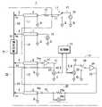
インピーダンス測定装置1は、Hc測定端子2、Hp測定端子3、Lp測定端子4、Lc測定端子5、測定ケーブル6,7,8,9、第1信号源10、第1切替器11、保護抵抗12、電圧測定部13、負帰還回路14、および処理部15を備えて、測定対象91のインピーダンスを測定可能に構成されている。 Theimpedance measuring device 1 includes anHc measuring terminal 2, anHp measuring terminal 3, anLp measuring terminal 4, anLc measuring terminal 5, a measuringcable 6, 7, 8, 9, afirst signal source 10, afirst switcher 11, and a protective resistor. Avoltage measuring unit 13, anegative feedback circuit 14, and aprocessing unit 15 are provided so as to be able to measure the impedance of themeasurement target 91.

第1信号源10は、一定周波数で、かつ予め規定された振幅の第1正弦波信号V1を基準電位(インピーダンス測定装置1の内部グランドGの電位。ゼロボルト)を基準として出力する。この第1正弦波信号V1は、第1切替器11、保護抵抗12、測定ケーブル6(同軸ケーブルやシールドケーブルで構成された測定ケーブル6の不図示の芯線)およびHc測定端子2を介して、測定対象91の一方の端子92に印加される。また、第1正弦波信号V1が一方の端子92に印加された状態においては、第1信号源10から測定対象91に正弦波信号である測定電流I1が流れる。また、第1信号源10は、本例では一例として処理部15によって制御されて、第1正弦波信号V1の出力動作を実行する。なお、保護抵抗12を使用しない構成であってもよいのは勿論である。 Thefirst signal source 10 outputs a first sine wave signal V1 having a constant frequency and a predetermined amplitude with reference to a reference potential (potential of the internal ground G of theimpedance measuring device 1; zero volt). The first sinusoidal signal V1 is transmitted via afirst switch 11, aprotection resistor 12, a measurement cable 6 (a core wire (not shown) of themeasurement cable 6 composed of a coaxial cable or a shielded cable), and anHc measurement terminal 2. It is applied to oneterminal 92 of themeasurement target 91. Further, in a state where the first sine wave signal V1 is applied to oneterminal 92, a measurement current I1 which is a sine wave signal flows from thefirst signal source 10 to themeasurement target 91. Further, thefirst signal source 10 is controlled by theprocessing unit 15 as an example in this example, and executes the output operation of the first sine wave signal V1. Of course, the structure may not use theprotection resistor 12.

第1切替器11は、一例として、リレーやアナログスイッチを用いて単極双投形の切替スイッチとして機能するように構成されている。また、第1切替器11は、処理部15によって制御されることにより、第1信号源10から出力される第1正弦波信号V1、および内部グランドGの電位のうちの一方を、測定対象91の一方の端子92に印加する。また、発明の理解を容易にするため、第1切替器11は、接点での接触抵抗値がゼロオームの理想的な切替スイッチとして機能するものとする。 As an example, thefirst switch 11 is configured to function as a single-pole double-throw type changeover switch by using a relay or an analog switch. Further, thefirst switch 11 is controlled by theprocessing unit 15 to measure one of the potentials of the first sine wave signal V1 output from thefirst signal source 10 and theinternal ground G 91. It is applied to one of theterminals 92. Further, in order to facilitate the understanding of the invention, thefirst switch 11 functions as an ideal changeover switch having a contact resistance value of zero ohm at the contact point.

電圧測定部13は、一対の測定端子(図示せず)のうちの一方の測定端子が測定ケーブル7(測定ケーブル6と同種のケーブルの不図示の芯線)を介してHp測定端子3に接続され、他方の測定端子が内部グランドGに接続されている。この構成により、電圧測定部13は、内部グランドGを基準としてHp測定端子3に発生する電圧を測定することにより、負帰還回路14によって後述するように測定対象91の他方の端子93が内部グランドGの電位に規定された状態では、測定対象91の両端子92,93間の電圧(両端間電圧)を測定して、処理部15に出力する。 In thevoltage measuring unit 13, one of the measuring terminals (not shown) of the pair of measuring terminals (not shown) is connected to theHp measuring terminal 3 via the measuring cable 7 (core wire of the same type of cable as the measuring cable 6 (not shown)). , The other measuring terminal is connected to the internal ground G. With this configuration, thevoltage measuring unit 13 measures the voltage generated in the Hp measuring terminal 3 with reference to the internal ground G, so that theother terminal 93 of themeasurement target 91 is internally grounded by thenegative feedback circuit 14 as described later. In the state defined by the potential of G, the voltage (voltage between both ends) between bothterminals 92 and 93 of themeasurement target 91 is measured and output to theprocessing unit 15.

負帰還回路14は、一例として、電流電圧変換器21、ベクトル電圧計22、第2信号源23、第2切替器26、増幅器24および電流測定部25を備えて構成されている。なお、処理部15も、後述するように、ベクトル電圧計22から出力される振幅比RTおよび位相差θ(具体的には、第1振幅比RT1および第1位相差θ1と、第2振幅比RT2および第2位相差θ2)に基づいて初期振幅A0および初期位相θ0を算出して第2信号源23に対して設定する各処理(第1測定処理、第2測定処理および振幅位相算出処理)、並びにベクトル電圧計22から出力される振幅比RTおよび位相差θに基づいて第2信号源23に対して設定する振幅Aおよび位相φ(第2正弦波信号V2の振幅、ひいては増幅正弦波信号V3の振幅、および第1正弦波信号V1に対する第2正弦波信号V2、ひいては増幅正弦波信号V3の位相)を微調整する負帰還制御処理を実行するため、負帰還回路14の一部を構成している。また、負帰還回路14は、その入力端子14aが測定ケーブル8(測定ケーブル6と同種のケーブルの不図示の芯線)を介してLp測定端子4に接続され、その出力端子14bが測定ケーブル9(測定ケーブル6と同種のケーブルの不図示の芯線)を介してLc測定端子5に接続されている。 As an example, thenegative feedback circuit 14 includes a current-voltage converter 21, avector voltmeter 22, asecond signal source 23, asecond switch 26, anamplifier 24, and acurrent measuring unit 25. As will be described later, theprocessing unit 15 also has an amplitude ratio RT and a phase difference θ (specifically, a first amplitude ratio RT1 and a first phase difference θ1 and a second amplitude ratio) output from thevector voltmeter 22. Each process (first measurement process, second measurement process and amplitude phase calculation process) that calculates the initial amplitude A0 and the initial phase θ0 based on RT2 and the second phase difference θ2) and sets them for thesecond signal source 23. , And the amplitude A and phase φ (amplitude of the second sine wave signal V2, and thus the amplified sine wave signal) set for thesecond signal source 23 based on the amplitude ratio RT and the phase difference θ output from thevector voltmeter 22. A part of thenegative feedback circuit 14 is configured to execute the negative feedback control process for finely adjusting the amplitude of V3 and the phase of the second sine wave signal V2 and the amplified sine wave signal V3 with respect to the first sine wave signal V1. is doing. Further, thenegative feedback circuit 14 has itsinput terminal 14a connected to theLp measurement terminal 4 via a measurement cable 8 (a core wire of the same type as the measurement cable 6 (not shown)), and itsoutput terminal 14b is a measurement cable 9 (a measurement cable 9 (a core wire of the same type as the measurement cable 6)). It is connected to theLc measurement terminal 5 via a core wire (not shown) of the same type as themeasurement cable 6.

各測定ケーブル6,7,8,9は、図1に示すように、対応する測定端子2,3,4,5が接続された一方の端部において、それぞれの外部導体(網組線)が配線L1,L2,L3を介して接続され、かつ他方の端部において、それぞれの外部導体(網組線)が内部グランドGに接続されている。 As shown in FIG. 1, eachmeasurement cable 6, 7, 8, 9 has an external conductor (braided wire) at one end to which thecorresponding measurement terminals 2, 3, 4, 5 are connected. It is connected via wirings L1, L2, and L3, and at the other end, each outer conductor (braided wire) is connected to the inner ground G.

電流電圧変換器21は、一例として、図2に示すように、非反転入力端子が内部グランドGに接続された演算増幅器21a、一端が入力端子14aに接続されると共に他端が演算増幅器21aの反転入力端子に接続された入力抵抗21b、および一端が演算増幅器21aの反転入力端子に接続されると共に他端が演算増幅器21aの出力端子に接続された帰還抵抗21cを備えて構成されている。この構成により、電流電圧変換器21は、測定ケーブル8およびLp測定端子4を介して測定対象91の他方の端子93に接続されているときに、他方の端子93から負帰還回路14への流入電流を電圧Viに変換して出力する。 As an example, the current-voltage converter 21 has anoperational amplifier 21a having a non-inverting input terminal connected to the internal ground G, one end connected to theinput terminal 14a, and the other end of theoperational amplifier 21a. It is configured to include aninput resistor 21b connected to an inverting input terminal, and afeedback resistor 21c having one end connected to the inverting input terminal of theoperational amplifier 21a and the other end connected to the output terminal of theoperational amplifier 21a. With this configuration, when the current-voltage converter 21 is connected to theother terminal 93 of themeasurement target 91 via themeasurement cable 8 and theLp measurement terminal 4, the inflow from theother terminal 93 to thenegative feedback circuit 14 The current is converted into a voltage Vi and output.

ベクトル電圧計22は、電流電圧変換器21から出力される電圧Viについての振幅比RTおよび位相差θを測定して出力する。この場合、振幅比RTとは、ベクトル電圧計22に入力される基準信号の振幅で電圧Viの振幅を除した値であり、位相差θとは、この基準信号の位相を基準として電圧Viに生じている位相のずれを示す値である。また、ベクトル電圧計22には、第1信号源10から出力される第1正弦波信号V1、および第2信号源23から出力される第2正弦波信号V2のうちの処理部15によって選択された一方が基準信号として入力される。 Thevector voltmeter 22 measures and outputs the amplitude ratio RT and the phase difference θ with respect to the voltage Vi output from the current-voltage converter 21. In this case, the amplitude ratio RT is a value obtained by dividing the amplitude of the voltage Vi by the amplitude of the reference signal input to thevector voltmeter 22, and the phase difference θ is the voltage Vi based on the phase of the reference signal. It is a value indicating the phase shift that has occurred. Further, thevector voltmeter 22 is selected by theprocessing unit 15 of the first sine wave signal V1 output from thefirst signal source 10 and the second sine wave signal V2 output from thesecond signal source 23. One is input as a reference signal.

第2信号源23は、第1正弦波信号V1と同一周波数で、かつ設定された振幅Aの第2正弦波信号V2を、設定された位相φだけ第1正弦波信号V1に対してずらして出力する。第2切替器26は、一例として、リレーやアナログスイッチを用いて単極双投形の切替スイッチとして機能するように構成されている。また、第2切替器26は、処理部15によって制御されることにより、第2信号源23から出力される第2正弦波信号V2、および内部グランドGの電位のうちの一方を、増幅器24の入力端子へ出力する。また、発明の理解を容易にするため、第2切替器26は、接点での接触抵抗値がゼロオームで、かつ信号遅延のない理想的な切替スイッチとして機能するものとする。 Thesecond signal source 23 shifts the second sine wave signal V2 having the same frequency as the first sine wave signal V1 and having the set amplitude A with respect to the first sine wave signal V1 by the set phase φ. Output. As an example, thesecond switch 26 is configured to function as a single-pole double-throw type changeover switch using a relay or an analog switch. Further, thesecond switch 26 controls one of the potentials of the second sine wave signal V2 output from thesecond signal source 23 and the internal ground G by being controlled by theprocessing unit 15, of theamplifier 24. Output to the input terminal. Further, in order to facilitate the understanding of the invention, thesecond switch 26 functions as an ideal changeover switch having a contact resistance value of zero ohm at a contact and no signal delay.

増幅器24は、第2正弦波信号V2を増幅正弦波信号V3に増幅して、その不図示の出力端子から負帰還回路14の出力端子14bに出力する。本例では、電流測定部25が、増幅器24の出力端子と負帰還回路14の出力端子14bとの間に介装されている。このため、増幅正弦波信号V3は、電流測定部25、出力端子14b、測定ケーブル9およびLp測定端子4を介して、測定対象91の他方の端子93に出力される。 Theamplifier 24 amplifies the second sine wave signal V2 into the amplified sine wave signal V3, and outputs the second sine wave signal V2 from the output terminal (not shown) to theoutput terminal 14b of thenegative feedback circuit 14. In this example, thecurrent measuring unit 25 is interposed between the output terminal of theamplifier 24 and theoutput terminal 14b of thenegative feedback circuit 14. Therefore, the amplified sine wave signal V3 is output to theother terminal 93 of themeasurement target 91 via thecurrent measurement unit 25, theoutput terminal 14b, themeasurement cable 9, and theLp measurement terminal 4.

電流測定部25は、一例として、増幅器24の出力端子と負帰還回路14の出力端子14bとの間に介装された検出抵抗25a、および検出抵抗25aの両端間の電圧(検出抵抗25aに流れる電流I2に比例して変化する電圧)を測定して、処理部15に出力する電圧計25bを備えて構成されている。 As an example, thecurrent measuring unit 25 has adetection resistance 25a interposed between the output terminal of theamplifier 24 and theoutput terminal 14b of thenegative feedback circuit 14, and a voltage between both ends of thedetection resistance 25a (flows to thedetection resistance 25a). It is configured to include avoltmeter 25b that measures (a voltage that changes in proportion to the current I2) and outputs it to theprocessing unit 15.

処理部15は、信号切替器、CPUおよびメモリ(いずれも図示せず)などを備えて構成されて、第1信号源10、第1切替器11、第2信号源23および第2切替器26に対する制御処理、上記の信号切替器で第1正弦波信号V1および第2正弦波信号V2のうちの一方を基準信号として選択してベクトル電圧計22に出力する信号選択処理、第1測定処理、第2測定処理、振幅位相算出処理、負帰還制御処理、並びにインピーダンス測定処理を実行する。 Theprocessing unit 15 includes a signal switch, a CPU, a memory (none of which is shown), and the like, and includes afirst signal source 10, afirst switch 11, asecond signal source 23, and asecond switch 26. Control processing for, signal selection processing for selecting one of the first sine wave signal V1 and the second sine wave signal V2 as a reference signal and outputting it to thevector voltmeter 22 by the above signal switch, first measurement processing, The second measurement process, the amplitude phase calculation process, the negative feedback control process, and the impedance measurement process are executed.

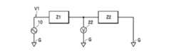
この場合、処理部15は、第1測定処理、第2測定処理および振幅位相算出処理を実行することにより、測定対象91が接続されたインピーダンス測定装置1に対して、重ね合わせの原理を適用して、ベクトル電圧計22で測定される振幅比RTがゼロになるために第2信号源23に対して設定すべき振幅Aとしての初期振幅A0および位相φとしての初期位相θ0を算出する。以下、第1測定処理、第2測定処理および振幅位相算出処理について説明する。なお、発明の理解を容易するため、図1に示すように測定対象91が接続されたインピーダンス測定装置1において、二点鎖線で囲まれた領域に含まれる複数の構成要素(保護抵抗12、測定ケーブル6、Hc測定端子2、一方の端子92、測定対象91、他方の端子93、Lp測定端子4、測定ケーブル8、および電流電圧変換器21)から成るインピーダンス部材全体のインピーダンスをZ1とし、一点鎖線で囲まれた領域に含まれる複数の構成要素(増幅器24、電流測定部25、測定ケーブル9、Lc測定端子5、他方の端子93、Lp測定端子4、測定ケーブル8、および電流電圧変換器21)から成るインピーダンス部材全体のインピーダンスをZ2とする。この場合、図1における第1測定処理、第2測定処理および振幅位相算出処理に関連する主たる構成要素は、図3に示す回路図で表される。 In this case, theprocessing unit 15 applies the principle of superimposition to theimpedance measuring device 1 to which themeasurement target 91 is connected by executing the first measurement processing, the second measurement processing, and the amplitude phase calculation processing. Therefore, the initial amplitude A0 as the amplitude A and the initial phase θ0 as the phase φ to be set for thesecond signal source 23 in order for the amplitude ratio RT measured by thevector voltmeter 22 to become zero are calculated. Hereinafter, the first measurement process, the second measurement process, and the amplitude phase calculation process will be described. In order to facilitate the understanding of the invention, in theimpedance measuring device 1 to which themeasurement target 91 is connected as shown in FIG. 1, a plurality of components (protection resistance 12, measurement) included in the region surrounded by the two-point chain line. The impedance of the entire impedance member consisting of thecable 6, theHc measurement terminal 2, oneterminal 92, themeasurement target 91, theother terminal 93, theLp measurement terminal 4, themeasurement cable 8 and the current-voltage converter 21) is set to Z1 and is one point. A plurality of components (amplifier 24, current measuringunit 25, measuringcable 9,Lc measuring terminal 5,other terminal 93,Lp measuring terminal 4, measuringcable 8, and current / voltage converter) included in the area surrounded by the chain wire. Let Z2 be the impedance of the entire impedance member made of 21). In this case, the main components related to the first measurement process, the second measurement process, and the amplitude phase calculation process in FIG. 1 are represented by the circuit diagram shown in FIG.

処理部15は、図4の回路図で示される回路(図3に示す回路図で表される回路において第1信号源10が単独で存在するときの回路)に基づいて第1測定処理を実行する。この第1測定処理では、処理部15は、第1切替器11に対する制御を実行して測定対象91の一方の端子92に第1正弦波信号V1を印加し、第2切替器26に対する制御を実行して増幅器24に内部グランドGの電位(基準電位)を出力し、かつ第1正弦波信号V1をベクトル電圧計22に基準信号として出力する。また、処理部15は、この状態においてベクトル電圧計22で測定される振幅比RTおよび位相差θを第1振幅比RT1および第1位相差θ1として取得して記憶する。 Theprocessing unit 15 executes the first measurement process based on the circuit shown in the circuit diagram of FIG. 4 (the circuit when thefirst signal source 10 exists alone in the circuit represented by the circuit diagram of FIG. 3). do. In this first measurement process, theprocessing unit 15 executes control for thefirst switch 11 and applies the first sine wave signal V1 to oneterminal 92 of themeasurement target 91 to control thesecond switch 26. This is executed to output the potential (reference potential) of the internal ground G to theamplifier 24 and output the first sine wave signal V1 to thevector voltmeter 22 as a reference signal. Further, theprocessing unit 15 acquires and stores the amplitude ratio RT and the phase difference θ measured by thevector voltmeter 22 in this state as the first amplitude ratio RT1 and the first phase difference θ1.

具体的に、第1信号源10から出力される第1正弦波信号V1を、例えば、A1×sin(ωt)としたときに、ベクトル電圧計22に印加される正弦波信号がB1×sin(ωt+θ1)となる場合には、ベクトル電圧計22は、振幅比RTとして(B1/A1)を出力し、位相差θとしてθ1を出力する。したがって、処理部15は、第1振幅比RT1(=B1/A1)および第1位相差θ1を記憶する。 Specifically, when the first sine wave signal V1 output from thefirst signal source 10 is, for example, A1 × sin (ωt), the sine wave signal applied to thevector voltmeter 22 is B1 × sin ( When ωt + θ1), thevector voltmeter 22 outputs (B1 / A1) as the amplitude ratio RT and outputs θ1 as the phase difference θ. Therefore, theprocessing unit 15 stores the first amplitude ratio RT1 (= B1 / A1) and the first phase difference θ1.

また、処理部15は、図5の回路図で示される回路(図3に示す回路図で表される回路において第2信号源23が単独で存在するときの回路)に基づいて第2測定処理を実行する。この第2測定処理では、処理部15は、第1切替器11に対する制御を実行して保護抵抗12の一端を内部グランドGの電位(基準電位)に接続し、第2切替器26に対する制御を実行して増幅器24に第2正弦波信号V2を出力し、かつ第2正弦波信号V2をベクトル電圧計22に基準信号として出力する。また、処理部15は、この状態においてベクトル電圧計22で測定される振幅比RTおよび位相差θを第2振幅比RT2および第2位相差θ2として取得して記憶する。 Further, theprocessing unit 15 performs the second measurement processing based on the circuit shown in the circuit diagram of FIG. 5 (the circuit when thesecond signal source 23 exists alone in the circuit represented by the circuit diagram of FIG. 3). To execute. In this second measurement process, theprocessing unit 15 executes control for thefirst switch 11 to connect one end of theprotection resistor 12 to the potential (reference potential) of the internal ground G, and controls thesecond switch 26. This is executed to output the second sine wave signal V2 to theamplifier 24 and output the second sine wave signal V2 to thevector voltmeter 22 as a reference signal. Further, theprocessing unit 15 acquires and stores the amplitude ratio RT and the phase difference θ measured by thevector voltmeter 22 in this state as the second amplitude ratio RT2 and the second phase difference θ2.

具体的に、第2信号源23から出力される第2正弦波信号V2を、例えば、A2×sin(ωt)としたときに、ベクトル電圧計22に印加される正弦波信号が、B2× sin(ωt+θ2) となる場合には、ベクトル電圧計22は、振幅比RTとして(B2/A2)を出力し、位相差θとしてθ2を出力する。したがって、処理部15は、第2振幅比RT2(=B2/A2)および第2位相差θ2を記憶する。 Specifically, when the second sine wave signal V2 output from thesecond signal source 23 is, for example, A2 × sin (ωt), the sine wave signal applied to thevector voltmeter 22 is B2 × sin. When (ωt + θ2) is obtained, thevector voltmeter 22 outputs (B2 / A2) as the amplitude ratio RT and outputs θ2 as the phase difference θ. Therefore, theprocessing unit 15 stores the second amplitude ratio RT2 (= B2 / A2) and the second phase difference θ2.

また、振幅位相算出処理では、処理部15は、上記した第1測定処理および第2測定処理において取得して記憶した第1振幅比RT1、第1位相差θ1、第2振幅比RT2および第2位相差θ2から、一方の端子92に第1正弦波信号V1が印加され、増幅器24の入力端子に第2正弦波信号V2が出力され、かつベクトル電圧計22に第1正弦波信号V1を基準信号として出力している状態において、ベクトル電圧計22で測定される振幅比RTがゼロになるために第2信号源23に対して設定すべき振幅A(初期振幅A0)および位相φ(初期位相θ0)を算出して、第2信号源23に設定する。 Further, in the amplitude phase calculation process, theprocessing unit 15 acquires and stores the first amplitude ratio RT1, the first phase difference θ1, the second amplitude ratio RT2, and the second in the first measurement process and the second measurement process described above. From the phase difference θ2, the first sine wave signal V1 is applied to oneterminal 92, the second sine wave signal V2 is output to the input terminal of theamplifier 24, and the first sine wave signal V1 is referred to to thevector voltmeter 22. Amplitude A (initial amplitude A0) and phase φ (initial phase) to be set for thesecond signal source 23 in order for the amplitude ratio RT measured by thevector voltmeter 22 to become zero in the state of being output as a signal. θ0) is calculated and set in thesecond signal source 23.

重ね合わせの原理によれば、図3に示す回路図で表される回路、すなわち、第1信号源10および第2信号源23が共に存在するときの回路において、ベクトル電圧計22に印加される電圧は、上記した正弦波信号:B1×sin(ωt+θ1)と、上記した正弦波信号:B2×sin(ωt+θ2)の合成信号となる。したがって、この合成信号の振幅が常にゼロボルトとなる条件(つまり、ベクトル電圧計22で測定される振幅比RTがゼロとなる条件)は、第1測定処理において測定される正弦波信号:B1×sin(ωt+θ1)に対して、第2測定処理において測定される正弦波信号:B2×sin(ωt+θ2)が、振幅が一致し、かつ位相が180°ずれていることが必要となる。 According to the principle of superposition, it is applied to thevector voltmeter 22 in the circuit represented by the circuit diagram shown in FIG. 3, that is, the circuit in which thefirst signal source 10 and thesecond signal source 23 are present together. The voltage is a composite signal of the above-mentioned sine wave signal: B1 × sin (ωt + θ1) and the above-mentioned sine wave signal: B2 × sin (ωt + θ2). Therefore, the condition that the amplitude of this combined signal is always zero volt (that is, the condition that the amplitude ratio RT measured by thevector voltmeter 22 is zero) is the sine wave signal measured in the first measurement process: B1 × sin. With respect to (ωt + θ1), it is necessary that the sine wave signal: B2 × sin (ωt + θ2) measured in the second measurement process has the same amplitude and is 180 ° out of phase.

この場合、正弦波信号:B1×sin(ωt+θ1)の振幅B1に、正弦波信号:B2×sin(ωt+θ2)の振幅B2が一致するためには、つまりB1=B2(A1×RT1=A2×RT2)となるためには、第2信号源23から出力される第2正弦波信号V2の振幅A2が下記式(1)で示される値となる必要がある。
A2=A1×RT1/RT2 ・・・(1)
In this case, in order for the amplitude B1 of the sine wave signal: B1 × sin (ωt + θ1) to match the amplitude B2 of the sine wave signal: B2 × sin (ωt + θ2), that is, B1 = B2 (A1 × RT1 = A2 × RT2). ), The amplitude A2 of the second sine wave signal V2 output from thesecond signal source 23 needs to be a value represented by the following equation (1).
A2 = A1 x RT1 / RT2 ... (1)

また、正弦波信号:B1×sin(ωt+θ1)に対して、正弦波信号:B2× sin(ωt+θ2) の位相が180°ずれるためには、第1信号源10から出力される第1正弦波信号V1の位相に対して、第2信号源23から出力される第2正弦波信号V2の位相が、下記式(2)で示される位相φだけずれる必要がある。
φ=θ1+π-θ2 ・・・(2)
つまり、第1正弦波信号V1の位相を基準として第2信号源23に対して位相φだけずらす設定を行った場合に、正弦波信号:B1×sin(ωt+θ1)は第1正弦波信号V1の位相に対して位相θ1だけずれるのに対して、正弦波信号:B2×sin(ωt+θ2)は第1正弦波信号V1の位相に対して、位相φと位相θ2の合計分(φ+θ2)だけずれる。この場合、合計分(φ+θ2)が、位相θ1に対してπだけ大きい。このことから次の式が成り立つ。
θ1+π=φ+θ2
Further, in order for the phase of the sine wave signal: B2 × sin (ωt + θ2) to be 180 ° out of phase with respect to the sine wave signal: B1 × sin (ωt + θ1), the first sine wave signal output from thefirst signal source 10 is obtained. It is necessary that the phase of the second sine wave signal V2 output from thesecond signal source 23 is deviated from the phase of V1 by the phase φ represented by the following equation (2).
φ = θ1 + π-θ2 ... (2)
That is, when the phase φ is set to be shifted with respect to thesecond signal source 23 with respect to the phase of the first sine wave signal V1, the sine wave signal: B1 × sin (ωt + θ1) is the first sine wave signal V1. While the phase θ1 is deviated from the phase, the sine wave signal: B2 × sin (ωt + θ2) is deviated from the phase of the first sine wave signal V1 by the total phase φ and the phase θ2 (φ + θ2). In this case, the total amount (φ + θ2) is larger by π with respect to the phase θ1. From this, the following equation holds.
θ1 + π = φ + θ2

したがって、処理部15は、振幅位相算出処理において、第1振幅比RT1、第1位相差θ1、第2振幅比RT2および第2位相差θ2を上記した式(1),(2)に代入することにより、ベクトル電圧計22で測定される振幅比RTがゼロになるために第2信号源23に対して設定すべき振幅Aとしての初期振幅A0(=A2)および位相φ(初期位相θ0)を算出して、第2信号源23に設定する。 Therefore, in the amplitude phase calculation process, theprocessing unit 15 substitutes the first amplitude ratio RT1, the first phase difference θ1, the second amplitude ratio RT2, and the second phase difference θ2 into the above equations (1) and (2). As a result, the initial amplitude A0 (= A2) and the phase φ (initial phase θ0) as the amplitude A to be set for thesecond signal source 23 in order for the amplitude ratio RT measured by thevector voltmeter 22 to become zero. Is calculated and set in thesecond signal source 23.

また、負帰還制御処理では、処理部15は、上記の初期振幅A0(=A2)および位相φ(初期位相θ0)を第2信号源23に設定した後であって、測定対象91の一方の端子92に第1正弦波信号V1を印加し、増幅器24の入力端子に第2正弦波信号V2を出力し、かつベクトル電圧計22に第1正弦波信号V1を基準信号として出力している状態において、ベクトル電圧計22で測定される振幅比RTおよび位相差θを検出しつつ、この振幅比RTがゼロに維持されるように、第2信号源23に設定する振幅Aや位相φを微調整する。その結果、Lp測定端子4の電圧が内部グランドGの電位に維持されて、測定対象91の他方の端子93が内部グランドGに等価的に接続されることになる。 Further, in the negative feedback control process, theprocessing unit 15 is one of the measurement targets 91 after the initial amplitude A0 (= A2) and the phase φ (initial phase θ0) are set in thesecond signal source 23. A state in which the first sine wave signal V1 is applied to the terminal 92, the second sine wave signal V2 is output to the input terminal of theamplifier 24, and the first sine wave signal V1 is output to thevector voltmeter 22 as a reference signal. In, while detecting the amplitude ratio RT and the phase difference θ measured by thevector voltmeter 22, the amplitude A and the phase φ set in thesecond signal source 23 are finely adjusted so that the amplitude ratio RT is maintained at zero. adjust. As a result, the voltage of theLp measurement terminal 4 is maintained at the potential of the internal ground G, and theother terminal 93 of themeasurement target 91 is equivalently connected to the internal ground G.

この場合、インピーダンス測定装置1を構成する各構成要素(例えば、第1信号源10や第2信号源23など)に、経時変化や温度変化が無い状態(理想状態)においては、第2信号源23に上記のようにして求めた初期振幅A0および初期位相θ0を設定するだけで、この負帰還制御処理を実行しなくても、ベクトル電圧計22で測定される振幅比RTはゼロに維持される(つまり、測定対象91の他方の端子93が内部グランドGに等価的に接続された状態が維持される)。しかしながら、現実には、インピーダンス測定装置1を構成する各構成要素(例えば、第1信号源10や第2信号源23など)には経時変化や温度変化が生じることから、処理部15は、この負帰還制御処理を実行することで、ベクトル電圧計22で測定される振幅比RTをゼロ(位相差θもゼロ)に維持する。 In this case, in a state (ideal state) in which each component (for example, thefirst signal source 10 or the second signal source 23) constituting theimpedance measuring device 1 does not change with time or temperature, the second signal source is used. By simply setting the initial amplitude A0 and the initial phase θ0 obtained as described above in 23, the amplitude ratio RT measured by thevector voltmeter 22 is maintained at zero even if this negative feedback control process is not executed. (That is, the state in which theother terminal 93 of themeasurement target 91 is equivalently connected to the internal ground G is maintained). However, in reality, each component (for example, thefirst signal source 10 or the second signal source 23) constituting theimpedance measuring device 1 undergoes a change with time or a temperature change, so that theprocessing unit 15 has this. By executing the negative feedback control process, the amplitude ratio RT measured by thevector voltmeter 22 is maintained at zero (the phase difference θ is also zero).

また、インピーダンス測定処理では、処理部15は、第2信号源23への初期振幅A0および初期位相θ0の設定により(本例では、加えて負帰還制御処理の実行により)、測定対象91の他方の端子93が内部グランドGに等価的に接続されている状態において、電圧測定部13で測定される測定対象91の両端子92,93間の両端間電圧と、電流測定部25で測定される電流I2とに基づいて、測定対象91のインピーダンスを算出する。測定対象91の他方の端子93が内部グランドGに等価的に接続されている状態では、電流電圧変換器21に流入する電流、つまり、Lp測定端子4から測定ケーブル8を介して負帰還回路14に流入する電流はゼロであることから、第1信号源10から測定対象91に流れる測定電流I1は、すべて電流I2として電流測定部25に流れる。したがって、電流測定部25は、測定対象91に流れる測定電流I1を電流I2として測定して処理部15に出力する。これにより、処理部15は、測定対象91のインピーダンスを正確に測定(算出)する。また、処理部15は、インピーダンス測定処理において、測定したインピーダンスを不図示の出力部(例えば、LCDなどの表示装置など)に出力する。 Further, in the impedance measurement process, theprocessing unit 15 sets the initial amplitude A0 and the initial phase θ0 to the second signal source 23 (in this example, by executing the negative feedback control process in addition), the other side of themeasurement target 91. The voltage between bothterminals 92 and 93 of themeasurement target 91 measured by thevoltage measuring unit 13 and the voltage between both ends measured by thecurrent measuring unit 25 in a state where theterminal 93 of the above is equivalently connected to the internal ground G. The impedance of themeasurement target 91 is calculated based on the current I2. In a state where theother terminal 93 of themeasurement target 91 is equivalently connected to the internal ground G, the current flowing into the current-voltage converter 21, that is, thenegative feedback circuit 14 from theLp measurement terminal 4 via themeasurement cable 8. Since the current flowing into the current is zero, all the measured current I1 flowing from thefirst signal source 10 to themeasurement target 91 flows to thecurrent measuring unit 25 as the current I2. Therefore, thecurrent measuring unit 25 measures the measured current I1 flowing through themeasurement target 91 as the current I2 and outputs it to theprocessing unit 15. As a result, theprocessing unit 15 accurately measures (calculates) the impedance of themeasurement target 91. Further, in the impedance measurement process, theprocessing unit 15 outputs the measured impedance to an output unit (for example, a display device such as an LCD) (not shown).

次に、インピーダンス測定装置1の動作について、インピーダンス測定装置1における負帰還回路14の調整動作(調整方法)と併せて、図面を参照して説明する。なお、インピーダンス測定装置1は、測定対象91に正常に接続されているものとする。 Next, the operation of theimpedance measuring device 1 will be described with reference to the drawings together with the adjusting operation (adjusting method) of thenegative feedback circuit 14 in theimpedance measuring device 1. It is assumed that theimpedance measuring device 1 is normally connected to themeasurement target 91.

この状態において、インピーダンス測定装置1では、処理部15が、まず、上記した第1測定処理、第2測定処理および振幅位相算出処理を順次実行することにより、第1振幅比RT1および第1位相差θ1と、第2振幅比RT2および第2位相差θ2とを算出(測定)すると共に、これらに基づいて初期振幅A0および初期位相θ0を算出して第2信号源23に対して設定する。なお、第1測定処理および第2測定処理については、いずれを先に実行してもよい。これにより、インピーダンス測定装置1では、上記の理想状態においては、ベクトル電圧計22で測定される振幅比RTおよび位相差θが共にゼロになり、測定対象91の他方の端子93が内部グランドGに等価的に接続される。 In this state, in theimpedance measuring device 1, theprocessing unit 15 first sequentially executes the first measurement processing, the second measurement processing, and the amplitude phase calculation processing described above, whereby the first amplitude ratio RT1 and the first phase difference are executed. The θ1 and the second amplitude ratio RT2 and the second phase difference θ2 are calculated (measured), and the initial amplitude A0 and the initial phase θ0 are calculated based on these and set for thesecond signal source 23. Either of the first measurement process and the second measurement process may be executed first. As a result, in theimpedance measuring device 1, in the above ideal state, both the amplitude ratio RT and the phase difference θ measured by thevector voltmeter 22 become zero, and theother terminal 93 of themeasurement target 91 becomes the internal ground G. Equivalently connected.

本例では、処理部15は、次いで、負帰還制御処理を実行することにより、ベクトル電圧計22で測定される振幅比RTが継続してゼロ(位相差θも継続してゼロ)に維持されて、測定対象91の他方の端子93が継続して内部グランドGに等価的に接続されるように、第2信号源23に設定する振幅Aや位相φを微調整する。 In this example, theprocessing unit 15 then executes the negative feedback control process, so that the amplitude ratio RT measured by thevector voltmeter 22 is continuously maintained at zero (the phase difference θ is also continuously zero). Then, the amplitude A and the phase φ set in thesecond signal source 23 are finely adjusted so that theother terminal 93 of themeasurement target 91 is continuously and equivalently connected to the internal ground G.

この状態では、電流電圧変換器21に流入する電流、つまり、Lp測定端子4から測定ケーブル8を介して負帰還回路14に流入する電流はゼロであることから、第1信号源10から測定対象91に流れる測定電流I1は、すべて電流I2として電流測定部25に流れる。したがって、電流測定部25は、測定対象91に流れる測定電流I1である電流I2を測定して処理部15に出力している。また、ベクトル電圧値Vscがゼロボルトに維持されていることから、測定対象91の他方の端子93は等価的に内部グランドGに接続された状態になっている。したがって、電圧測定部13は、内部グランドGを基準としてHp測定端子3に発生する電圧を測定することにより、測定対象91の両端子92,93間の電圧(両端間電圧)を測定して、処理部15に出力する。 In this state, the current flowing into the current-voltage converter 21, that is, the current flowing from theLp measuring terminal 4 to thenegative feedback circuit 14 via the measuringcable 8 is zero, so that the measurement target is from thefirst signal source 10. All the measured current I1 flowing through the 91 flows to thecurrent measuring unit 25 as the current I2. Therefore, thecurrent measuring unit 25 measures the current I2, which is the measured current I1 flowing through themeasurement target 91, and outputs the current to theprocessing unit 15. Further, since the vector voltage value Vsc is maintained at zero volt, theother terminal 93 of themeasurement target 91 is equivalently connected to the internal ground G. Therefore, thevoltage measuring unit 13 measures the voltage between bothterminals 92 and 93 of the measurement target 91 (voltage between both ends) by measuring the voltage generated at the Hp measuring terminal 3 with the internal ground G as a reference. Output to theprocessing unit 15.

次いで、処理部15は、この状態において、インピーダンス測定処理を実行して、電圧測定部13で測定される測定対象91の両端子92,93間の両端間電圧と、電流測定部25で測定される電流I2とに基づいて、測定対象91のインピーダンスを正確に算出する。また、算出したインピーダンスを出力部に出力する。 Next, theprocessing unit 15 executes impedance measurement processing in this state, and measures the voltage between bothterminals 92 and 93 of themeasurement target 91 measured by thevoltage measurement unit 13 and thecurrent measurement unit 25. The impedance of themeasurement target 91 is accurately calculated based on the current I2. In addition, the calculated impedance is output to the output unit.

このように、このインピーダンス測定装置1では、処理部15は、第1測定処理、第2測定処理および振幅位相算出処理を実行して、ベクトル電圧計22で測定される振幅比RTがゼロ(位相差θもゼロ)となるように、第2信号源23に対して設定すべき振幅Aとしての初期振幅A0および位相φとしての初期位相θ0を算出して設定する。 As described above, in theimpedance measuring device 1, theprocessing unit 15 executes the first measurement processing, the second measurement processing, and the amplitude phase calculation processing, and the amplitude ratio RT measured by thevector voltmeter 22 is zero (position). The initial amplitude A0 as the amplitude A to be set for thesecond signal source 23 and the initial phase θ0 as the phase φ are calculated and set so that the phase difference θ is also zero).

したがって、このインピーダンス測定装置1、およびインピーダンス測定装置1における負帰還回路14の調整方法によれば、狭帯域高利得増幅器を備えたヌル増幅手段(負帰還回路)が負帰還動作を実行して、狭帯域高利得増幅器に内蔵された積分器から出力される直流信号を目的の電圧値に移行させる(これにより、測定対象の他方の端子の電位を接地電位(本例での内部グランドGの電位)に移行させる)とのインピーダンス測定装置における負帰還回路の調整方法、およびこの調整方法を実行するインピーダンス測定装置と比較して、積分器を使用していないために、測定対象91の他方の端子93が内部グランドGに等価的に接続される(測定対象91の他方の端子93の電位を内部グランドGの電位(接地電位)とする)までに要する時間を大幅に短縮することができる。また、このインピーダンス測定装置1によれば、回路構成の複雑な狭帯域高利得増幅器を不要にすることができることから、装置コストを十分に低減することができる。 Therefore, according to theimpedance measuring device 1 and the adjustment method of thenegative feedback circuit 14 in theimpedance measuring device 1, the null amplification means (negative feedback circuit) provided with the narrow band high gain amplifier executes the negative feedback operation. The DC signal output from the integrator built into the narrow band high gain amplifier is transferred to the target voltage value (this causes the potential of the other terminal to be measured to be the ground potential (the potential of the internal ground G in this example). The other terminal of themeasurement target 91 because the integrator is not used in comparison with the method of adjusting the negative feedback circuit in the impedance measuring device and the impedance measuring device that executes this adjustment method. The time required for 93 to be equivalently connected to the internal ground G (the potential of theother terminal 93 of themeasurement target 91 is set to the potential of the internal ground G (ground potential)) can be significantly shortened. Further, according to theimpedance measuring device 1, since it is possible to eliminate the need for a narrow band high gain amplifier having a complicated circuit configuration, the device cost can be sufficiently reduced.

1 インピーダンス測定装置
10 第1信号源
11 第1切替器
14 負帰還回路
15 処理部
21 電流電圧変換器
22 ベクトル電圧計
23 第2信号源
24 増幅器
25 電流測定部
26 第2切替器
91 測定対象
92 一方の端子
93 他方の端子
A 振幅
G 内部グランド
I2 電流
RT 振幅比
V1 第1正弦波信号
V2 第2正弦波信号
V3 増幅正弦波信号
Vi 電圧
θ 位相差
φ 位相
1Impedance measuring device 101st signal source 111st switch 14Negative feedback circuit 15Processing unit 21Current voltage converter 22Vector voltmeter 232nd signal source 24Amplifier 25Current measuring unit 262nd switch 91Measurement target 92 Oneterminal 93 The other terminal
A amplitude
G Internal ground I2 Current RT Amplitude ratio V1 First sine wave signal V2 Second sine wave signal V3 Amplified sine wave signal Vi voltage
θ phase difference
φ phase

Claims (2)

Translated fromJapanese
一定周波数で、かつ予め規定された振幅の第1正弦波信号を測定対象の一方の端子に印加する第1信号源と、
前記一方の端子に前記第1正弦波信号が印加されている状態において、前記測定対象の他方の端子を基準電位に規定する負帰還回路とを備え、当該負帰還回路によって前記他方の端子が前記基準電位に規定されているときの前記一方の端子の電圧と当該負帰還回路に流れる電流とに基づいて前記測定対象のインピーダンスを測定するインピーダンス測定装置であって、
前記負帰還回路は、
前記他方の端子に接続されて、当該他方の端子からの流入電流を電圧に変換して出力する電流電圧変換器と、
前記電流電圧変換器から出力される前記電圧についての基準信号に対する振幅比および位相差を測定するベクトル電圧計と、
前記第1正弦波信号と同一周波数で、かつ設定された振幅の第2正弦波信号を、設定された位相だけ当該第1正弦波信号に対してずらして出力する第2信号源と、
前記第2正弦波信号を増幅正弦波信号に増幅して出力端子から前記測定対象の他方の端子に出力する増幅器と、
前記他方の端子と前記増幅器の前記出力端子との間に介装されて、当該他方の端子と当該出力端子との間に流れる電流を測定する電流測定部と、
前記ベクトル電圧計で測定される前記振幅比および前記位相差に基づいて、当該振幅比がゼロに近づくように前記第2信号源に対して設定する前記振幅および前記位相を調整する負帰還制御処理を実行する処理部とを備えて構成され、
前記第1信号源と前記一方の端子との間に配設されて、前記第1正弦波信号および前記基準電位のうちの選択された一方を当該一方の端子に印加する第1切替器と、
前記第2信号源と前記増幅器との間に配設されて、前記第2正弦波信号および前記基準電位のうちの選択された一方を当該増幅器に出力する第2切替器とを備え、
前記処理部は、
前記第1切替器に対する制御を実行して前記一方の端子に前記第1正弦波信号を印加し、前記第2切替器に対する制御を実行して前記増幅器に前記基準電位を出力し、かつ前記第1正弦波信号を前記基準信号として、前記ベクトル電圧計で測定される前記振幅比および前記位相差をそれぞれ第1振幅比および第1位相差として取得する第1測定処理と、
前記第1切替器に対する制御を実行して前記一方の端子に前記基準電位を印加し、前記第2切替器に対する制御を実行して前記増幅器に前記第2正弦波信号を出力し、かつ当該第2正弦波信号を前記基準信号として、前記ベクトル電圧計で測定される前記振幅比および前記位相差をそれぞれ第2振幅比および第2位相差として取得する第2測定処理と、
前記第1切替器に対する制御を実行して前記一方の端子に前記第1正弦波信号を印加し、前記第2切替器に対する制御を実行して前記増幅器に前記第2正弦波信号を出力し、かつ前記第1正弦波信号を前記基準信号とした状態において前記ベクトル電圧計で測定される前記振幅比がゼロになるために前記第2信号源に対して設定すべき前記振幅および前記位相を、前記第1振幅比、前記第1位相差、前記第2振幅比および前記第2位相差から算出して当該第2信号源に設定する振幅位相算出処理とを実行するインピーダンス測定装置。
A first signal source that applies a first sine wave signal with a constant frequency and a predetermined amplitude to one terminal to be measured, and
In a state where the first sine wave signal is applied to the one terminal, the other terminal to be measured is provided with a negative feedback circuit that defines the other terminal as a reference potential, and the other terminal is caused by the negative feedback circuit. An impedance measuring device that measures the impedance of the measurement target based on the voltage of one of the terminals when specified in the reference potential and the current flowing through the negative feedback circuit.
The negative feedback circuit
A current-voltage converter that is connected to the other terminal and converts the inflow current from the other terminal into a voltage for output.
A vector voltmeter that measures the amplitude ratio and phase difference of the voltage output from the current-voltage converter with respect to the reference signal, and
A second signal source that outputs a second sine wave signal having the same frequency as the first sine wave signal and having a set amplitude by shifting the second sine wave signal by the set phase with respect to the first sine wave signal.
An amplifier that amplifies the second sine wave signal into an amplified sine wave signal and outputs it from the output terminal to the other terminal of the measurement target.
A current measuring unit that is interposed between the other terminal and the output terminal of the amplifier and measures the current flowing between the other terminal and the output terminal.
Negative feedback control processing that adjusts the amplitude and phase set for the second signal source so that the amplitude ratio approaches zero based on the amplitude ratio and the phase difference measured by the vector voltmeter. It is configured with a processing unit to execute
A first switch disposed between the first signal source and the one terminal and applying a selected one of the first sine wave signal and the reference potential to the one terminal.
A second switch disposed between the second signal source and the amplifier and outputting the selected one of the second sine wave signal and the reference potential to the amplifier is provided.
The processing unit
The control for the first switch is executed to apply the first sine wave signal to the one terminal, the control for the second switch is executed, the reference potential is output to the amplifier, and the reference potential is output to the amplifier. 1 The first measurement process of acquiring the amplitude ratio and the phase difference measured by the vector voltmeter as the first amplitude ratio and the first phase difference, respectively, using the sine wave signal as the reference signal.
The control for the first switch is executed to apply the reference potential to the one terminal, the control for the second switch is executed, the second sine wave signal is output to the amplifier, and the second sine wave signal is output. The second measurement process of acquiring the amplitude ratio and the phase difference measured by the vector voltmeter as the second amplitude ratio and the second phase difference, respectively, using the two sine wave signals as the reference signal.
The control for the first switch is executed to apply the first sine wave signal to the one terminal, the control for the second switch is executed, and the second sine wave signal is output to the amplifier. In addition, the amplitude and the phase to be set for the second signal source in order for the amplitude ratio measured by the vector voltmeter to become zero in a state where the first sinusoidal signal is used as the reference signal, are used. An impedance measuring device that executes an amplitude phase calculation process calculated from the first amplitude ratio, the first phase difference, the second amplitude ratio, and the second phase difference and set in the second signal source.
一定周波数で、かつ予め規定された振幅の第1正弦波信号を測定対象の一方の端子に印加する第1信号源と、
前記一方の端子に前記第1正弦波信号が印加されている状態において、前記測定対象の他方の端子を基準電位に規定する負帰還回路とを備え、当該負帰還回路によって前記他方の端子が前記基準電位に規定されているときの前記一方の端子の電圧と当該負帰還回路に流れる電流とに基づいて前記測定対象のインピーダンスを測定するインピーダンス測定装置であって、
前記負帰還回路は、
前記他方の端子に接続されて、当該他方の端子からの流入電流を電圧に変換して出力する電流電圧変換器と、
前記電流電圧変換器から出力される前記電圧についての基準信号に対する振幅比および位相差を測定するベクトル電圧計と、
前記第1正弦波信号と同一周波数で、かつ設定された振幅の第2正弦波信号を、設定された位相だけ当該第1正弦波信号に対してずらして出力する第2信号源と、
前記第2正弦波信号を増幅正弦波信号に増幅して出力端子から前記測定対象の他方の端子に出力する増幅器と、
前記他方の端子と前記増幅器の前記出力端子との間に介装されて、当該他方の端子と当該出力端子との間に流れる電流を測定する電流測定部と、
前記ベクトル電圧計で測定される前記振幅比および前記位相差に基づいて、当該振幅比がゼロに近づくように前記第2信号源に対して設定する前記振幅および前記位相を調整する負帰還制御処理を実行する処理部とを備えて構成されているインピーダンス測定装置における負帰還回路の調整方法であって、
前記一方の端子に前記第1正弦波信号を印加し、前記増幅器に前記基準電位を出力し、かつ前記第1正弦波信号を前記基準信号として、前記ベクトル電圧計で測定される前記振幅比および前記位相差をそれぞれ第1振幅比および第1位相差として取得する第1測定処理と、
前記一方の端子に前記基準電位を印加し、前記増幅器に前記第2正弦波信号を出力し、かつ当該第2正弦波信号を前記基準信号として、前記ベクトル電圧計で測定される前記振幅比および前記位相差をそれぞれ第2振幅比および第2位相差として取得する第2測定処理と、
前記一方の端子に前記第1正弦波信号を印加し、前記増幅器に前記第2正弦波信号を出力し、かつ前記第1正弦波信号を前記基準信号とした状態において前記ベクトル電圧計で測定される前記振幅比がゼロになるために前記第2信号源に対して設定すべき前記振幅および前記位相を、前記第1振幅比、前記第1位相差、前記第2振幅比および前記第2位相差から算出して当該第2信号源に設定する振幅位相算出処理とを実行するインピーダンス測定装置における負帰還回路の調整方法。
A first signal source that applies a first sine wave signal with a constant frequency and a predetermined amplitude to one terminal to be measured, and
In a state where the first sine wave signal is applied to the one terminal, the other terminal to be measured is provided with a negative feedback circuit that defines the other terminal as a reference potential, and the other terminal is caused by the negative feedback circuit. An impedance measuring device that measures the impedance of the measurement target based on the voltage of one of the terminals when specified in the reference potential and the current flowing through the negative feedback circuit.
The negative feedback circuit
A current-voltage converter that is connected to the other terminal and converts the inflow current from the other terminal into a voltage for output.
A vector voltmeter that measures the amplitude ratio and phase difference of the voltage output from the current-voltage converter with respect to the reference signal, and
A second signal source that outputs a second sine wave signal having the same frequency as the first sine wave signal and having a set amplitude by shifting the second sine wave signal by the set phase with respect to the first sine wave signal.
An amplifier that amplifies the second sine wave signal into an amplified sine wave signal and outputs it from the output terminal to the other terminal of the measurement target.
A current measuring unit that is interposed between the other terminal and the output terminal of the amplifier and measures the current flowing between the other terminal and the output terminal.
Negative feedback control processing that adjusts the amplitude and phase set for the second signal source so that the amplitude ratio approaches zero based on the amplitude ratio and the phase difference measured by the vector voltmeter. It is a method of adjusting a negative feedback circuit in an impedance measuring device configured to include a processing unit for executing the above.
The amplitude ratio and the amplitude ratio measured by the vector voltmeter, the first sine wave signal is applied to the one terminal, the reference potential is output to the amplifier, and the first sine wave signal is used as the reference signal. The first measurement process for acquiring the phase difference as the first amplitude ratio and the first phase difference, respectively.
The reference potential is applied to the one terminal, the second sine wave signal is output to the amplifier, and the second sine wave signal is used as the reference signal, and the amplitude ratio and the amplitude ratio measured by the vector voltmeter are used. The second measurement process for acquiring the phase difference as the second amplitude ratio and the second phase difference, respectively.
The first sine wave signal is applied to the one terminal, the second sine wave signal is output to the amplifier, and the first sine wave signal is used as the reference signal, and the measurement is performed by the vector voltmeter. The amplitude and the phase to be set for the second signal source in order for the amplitude ratio to become zero are the first amplitude ratio, the first phase difference, the second amplitude ratio, and the second position. A method for adjusting a negative feedback circuit in an impedance measuring device that executes an amplitude phase calculation process that is calculated from a phase difference and set in the second signal source.
JP2018195004A2018-10-162018-10-16 How to adjust the negative feedback circuit in the impedance measuring device and the impedance measuring deviceActiveJP7094190B2 (en)

Priority Applications (3)

Application NumberPriority DateFiling DateTitle
JP2018195004AJP7094190B2 (en)2018-10-162018-10-16 How to adjust the negative feedback circuit in the impedance measuring device and the impedance measuring device
CN201980066106.2ACN112840217B (en)2018-10-162019-06-20Impedance measuring device and method for adjusting negative feedback circuit in impedance measuring device
PCT/JP2019/024435WO2020079888A1 (en)2018-10-162019-06-20Impedance measurement device and method for adjusting negative feedback circuit in impedance measurement device

Applications Claiming Priority (1)

Application NumberPriority DateFiling DateTitle
JP2018195004AJP7094190B2 (en)2018-10-162018-10-16 How to adjust the negative feedback circuit in the impedance measuring device and the impedance measuring device

Publications (2)

Publication NumberPublication Date
JP2020063943A JP2020063943A (en)2020-04-23
JP7094190B2true JP7094190B2 (en)2022-07-01

Family

ID=70284500

Family Applications (1)

Application NumberTitlePriority DateFiling Date
JP2018195004AActiveJP7094190B2 (en)2018-10-162018-10-16 How to adjust the negative feedback circuit in the impedance measuring device and the impedance measuring device

Country Status (3)

CountryLink
JP (1)JP7094190B2 (en)
CN (1)CN112840217B (en)
WO (1)WO2020079888A1 (en)

Families Citing this family (4)

* Cited by examiner, † Cited by third party
Publication numberPriority datePublication dateAssigneeTitle
CN114113794B (en)*2021-11-222024-03-26哈尔滨工业大学(深圳)Sinusoidal excitation-based conductive cable impedance single-end detection method
CN114305382B (en)*2021-12-282025-08-22重庆金山医疗技术研究院有限公司 Esophageal impedance detection circuit, device and method
JP7723614B2 (en)*2022-01-212025-08-14日置電機株式会社 Impedance measurement device and method
US12345746B2 (en)2023-08-242025-07-01Novatek Microelectronics Corp.Voltage meter for measuring signal inside integrated circuit

Citations (6)

* Cited by examiner, † Cited by third party
Publication numberPriority datePublication dateAssigneeTitle
JP2003279607A (en)2002-03-252003-10-02Hioki Ee Corp Automatic balance circuit for impedance measurement
JP2004317391A (en)2003-04-182004-11-11Agilent Technol Inc Current-voltage converter and impedance measuring device
JP2007051905A (en)2005-08-172007-03-01Hioki Ee Corp Automatic balancing circuit for impedance measurement
JP3930586B2 (en)1996-07-262007-06-13アジレント・テクノロジーズ・インク Feedback loop stabilization method for impedance measuring device
JP2007232604A (en)2006-03-022007-09-13Agilent Technol Inc Current-voltage converter and impedance measuring device
JP2009270942A (en)2008-05-082009-11-19Hioki Ee CorpImpedance measuring device and impedance measuring method

Family Cites Families (7)

* Cited by examiner, † Cited by third party
Publication numberPriority datePublication dateAssigneeTitle
JP2846926B2 (en)*1990-05-251999-01-13株式会社アドバンテスト Impedance measuring device
JP3851375B2 (en)*1996-04-182006-11-29アジレント・テクノロジーズ・インク Impedance measuring device
TW418323B (en)*1998-02-192001-01-11Sumitomo Metal IndCapacitance detection system and method
US7391257B1 (en)*2007-01-312008-06-24Medtronic, Inc.Chopper-stabilized instrumentation amplifier for impedance measurement
CN103513211B (en)*2013-10-252016-03-02国家电网公司Ac impedance measurement measuring device
CN106526321B (en)*2015-09-152020-03-13日置电机株式会社Impedance measuring device and impedance measuring method
CN107449949B (en)*2017-09-062023-06-27常州同惠电子股份有限公司Device for applying DC bias voltage to AC sine wave signal source

Patent Citations (6)

* Cited by examiner, † Cited by third party
Publication numberPriority datePublication dateAssigneeTitle
JP3930586B2 (en)1996-07-262007-06-13アジレント・テクノロジーズ・インク Feedback loop stabilization method for impedance measuring device
JP2003279607A (en)2002-03-252003-10-02Hioki Ee Corp Automatic balance circuit for impedance measurement
JP2004317391A (en)2003-04-182004-11-11Agilent Technol Inc Current-voltage converter and impedance measuring device
JP2007051905A (en)2005-08-172007-03-01Hioki Ee Corp Automatic balancing circuit for impedance measurement
JP2007232604A (en)2006-03-022007-09-13Agilent Technol Inc Current-voltage converter and impedance measuring device
JP2009270942A (en)2008-05-082009-11-19Hioki Ee CorpImpedance measuring device and impedance measuring method

Also Published As

Publication numberPublication date
CN112840217A (en)2021-05-25
JP2020063943A (en)2020-04-23
WO2020079888A1 (en)2020-04-23
CN112840217B (en)2023-09-22

Similar Documents

PublicationPublication DateTitle
JP7094190B2 (en) How to adjust the negative feedback circuit in the impedance measuring device and the impedance measuring device
US4128805A (en)Method and apparatus for locating a fault on a line
CN109765429B (en)Impedance measuring system and impedance measuring method
WO2018059232A1 (en)Structure and method for testing lock-in amplifier
WO2020095471A1 (en)Impedance measurement device
US11804911B2 (en)Measurement apparatus
CN107064644B (en) Conductor AC resistance measurement method and system
JP2007033286A (en) Impedance measuring method and impedance measuring instrument
CN105388348A (en)Enhanced-type automatic balance bridge and open-loop compensation realization method thereof
JP7146558B2 (en) Impedance measuring device and adjustment method of negative feedback circuit in impedance measuring device
JP6774848B2 (en) Impedance measuring device
JP2023107029A5 (en)
JP4741900B2 (en) Automatic balancing circuit for impedance measurement
JP7723615B2 (en) Impedance measurement system and method
JP2573789B2 (en) Insulation resistance measuring device
JPH0368350B2 (en)
US20150168189A1 (en)Method for determination of the time of flight of the signals in the signal paths of a coriolis flow meter
TWI447401B (en)Method for circuit stability compensation
JP3992961B2 (en) Adjustment method of automatic balance circuit for impedance measurement and detection resistance measurement method of automatic balance circuit
JP2696510B2 (en) Measurement method of insulation resistance of electric circuit
JP5942506B2 (en) Earth leakage detector
JP3837110B2 (en) Double balanced mixer carrier leak measurement device
KR0182194B1 (en) 3-phase current detection method and apparatus
JP3863097B2 (en) Carrier leak measurement method for double balanced mixer
JPH0792273A (en)Metal detector

Legal Events

DateCodeTitleDescription
A621Written request for application examination

Free format text:JAPANESE INTERMEDIATE CODE: A621

Effective date:20210825

TRDDDecision of grant or rejection written
A01Written decision to grant a patent or to grant a registration (utility model)

Free format text:JAPANESE INTERMEDIATE CODE: A01

Effective date:20220607

A61First payment of annual fees (during grant procedure)

Free format text:JAPANESE INTERMEDIATE CODE: A61

Effective date:20220621

R150Certificate of patent or registration of utility model

Ref document number:7094190

Country of ref document:JP

Free format text:JAPANESE INTERMEDIATE CODE: R150

R250Receipt of annual fees

Free format text:JAPANESE INTERMEDIATE CODE: R250


[8]ページ先頭

©2009-2025 Movatter.jp