JP7094154B2 - Film forming equipment and film forming method - Google Patents
Film forming equipment and film forming methodDownload PDFInfo
- Publication number
- JP7094154B2 JP7094154B2JP2018112585AJP2018112585AJP7094154B2JP 7094154 B2JP7094154 B2JP 7094154B2JP 2018112585 AJP2018112585 AJP 2018112585AJP 2018112585 AJP2018112585 AJP 2018112585AJP 7094154 B2JP7094154 B2JP 7094154B2
- Authority
- JP
- Japan
- Prior art keywords
- voltage
- film
- power supply
- high frequency
- film forming
- Prior art date
- Legal status (The legal status is an assumption and is not a legal conclusion. Google has not performed a legal analysis and makes no representation as to the accuracy of the status listed.)
- Active
Links
Images


Classifications
- H—ELECTRICITY
- H01—ELECTRIC ELEMENTS
- H01J—ELECTRIC DISCHARGE TUBES OR DISCHARGE LAMPS
- H01J37/00—Discharge tubes with provision for introducing objects or material to be exposed to the discharge, e.g. for the purpose of examination or processing thereof
- H01J37/32—Gas-filled discharge tubes
- H01J37/32009—Arrangements for generation of plasma specially adapted for examination or treatment of objects, e.g. plasma sources
- H01J37/32018—Glow discharge
- H01J37/32027—DC powered
- C—CHEMISTRY; METALLURGY
- C23—COATING METALLIC MATERIAL; COATING MATERIAL WITH METALLIC MATERIAL; CHEMICAL SURFACE TREATMENT; DIFFUSION TREATMENT OF METALLIC MATERIAL; COATING BY VACUUM EVAPORATION, BY SPUTTERING, BY ION IMPLANTATION OR BY CHEMICAL VAPOUR DEPOSITION, IN GENERAL; INHIBITING CORROSION OF METALLIC MATERIAL OR INCRUSTATION IN GENERAL
- C23C—COATING METALLIC MATERIAL; COATING MATERIAL WITH METALLIC MATERIAL; SURFACE TREATMENT OF METALLIC MATERIAL BY DIFFUSION INTO THE SURFACE, BY CHEMICAL CONVERSION OR SUBSTITUTION; COATING BY VACUUM EVAPORATION, BY SPUTTERING, BY ION IMPLANTATION OR BY CHEMICAL VAPOUR DEPOSITION, IN GENERAL
- C23C16/00—Chemical coating by decomposition of gaseous compounds, without leaving reaction products of surface material in the coating, i.e. chemical vapour deposition [CVD] processes
- C23C16/22—Chemical coating by decomposition of gaseous compounds, without leaving reaction products of surface material in the coating, i.e. chemical vapour deposition [CVD] processes characterised by the deposition of inorganic material, other than metallic material
- C23C16/30—Deposition of compounds, mixtures or solid solutions, e.g. borides, carbides, nitrides
- C23C16/40—Oxides
- C23C16/405—Oxides of refractory metals or yttrium
- C—CHEMISTRY; METALLURGY
- C23—COATING METALLIC MATERIAL; COATING MATERIAL WITH METALLIC MATERIAL; CHEMICAL SURFACE TREATMENT; DIFFUSION TREATMENT OF METALLIC MATERIAL; COATING BY VACUUM EVAPORATION, BY SPUTTERING, BY ION IMPLANTATION OR BY CHEMICAL VAPOUR DEPOSITION, IN GENERAL; INHIBITING CORROSION OF METALLIC MATERIAL OR INCRUSTATION IN GENERAL
- C23C—COATING METALLIC MATERIAL; COATING MATERIAL WITH METALLIC MATERIAL; SURFACE TREATMENT OF METALLIC MATERIAL BY DIFFUSION INTO THE SURFACE, BY CHEMICAL CONVERSION OR SUBSTITUTION; COATING BY VACUUM EVAPORATION, BY SPUTTERING, BY ION IMPLANTATION OR BY CHEMICAL VAPOUR DEPOSITION, IN GENERAL
- C23C16/00—Chemical coating by decomposition of gaseous compounds, without leaving reaction products of surface material in the coating, i.e. chemical vapour deposition [CVD] processes
- C23C16/44—Chemical coating by decomposition of gaseous compounds, without leaving reaction products of surface material in the coating, i.e. chemical vapour deposition [CVD] processes characterised by the method of coating
- C23C16/455—Chemical coating by decomposition of gaseous compounds, without leaving reaction products of surface material in the coating, i.e. chemical vapour deposition [CVD] processes characterised by the method of coating characterised by the method used for introducing gases into reaction chamber or for modifying gas flows in reaction chamber
- C23C16/45523—Pulsed gas flow or change of composition over time
- C23C16/45525—Atomic layer deposition [ALD]
- C23C16/45527—Atomic layer deposition [ALD] characterized by the ALD cycle, e.g. different flows or temperatures during half-reactions, unusual pulsing sequence, use of precursor mixtures or auxiliary reactants or activations
- C23C16/45536—Use of plasma, radiation or electromagnetic fields
- C—CHEMISTRY; METALLURGY
- C23—COATING METALLIC MATERIAL; COATING MATERIAL WITH METALLIC MATERIAL; CHEMICAL SURFACE TREATMENT; DIFFUSION TREATMENT OF METALLIC MATERIAL; COATING BY VACUUM EVAPORATION, BY SPUTTERING, BY ION IMPLANTATION OR BY CHEMICAL VAPOUR DEPOSITION, IN GENERAL; INHIBITING CORROSION OF METALLIC MATERIAL OR INCRUSTATION IN GENERAL
- C23C—COATING METALLIC MATERIAL; COATING MATERIAL WITH METALLIC MATERIAL; SURFACE TREATMENT OF METALLIC MATERIAL BY DIFFUSION INTO THE SURFACE, BY CHEMICAL CONVERSION OR SUBSTITUTION; COATING BY VACUUM EVAPORATION, BY SPUTTERING, BY ION IMPLANTATION OR BY CHEMICAL VAPOUR DEPOSITION, IN GENERAL
- C23C16/00—Chemical coating by decomposition of gaseous compounds, without leaving reaction products of surface material in the coating, i.e. chemical vapour deposition [CVD] processes
- C23C16/44—Chemical coating by decomposition of gaseous compounds, without leaving reaction products of surface material in the coating, i.e. chemical vapour deposition [CVD] processes characterised by the method of coating
- C23C16/455—Chemical coating by decomposition of gaseous compounds, without leaving reaction products of surface material in the coating, i.e. chemical vapour deposition [CVD] processes characterised by the method of coating characterised by the method used for introducing gases into reaction chamber or for modifying gas flows in reaction chamber
- C23C16/45563—Gas nozzles
- C23C16/45568—Porous nozzles
- C—CHEMISTRY; METALLURGY
- C23—COATING METALLIC MATERIAL; COATING MATERIAL WITH METALLIC MATERIAL; CHEMICAL SURFACE TREATMENT; DIFFUSION TREATMENT OF METALLIC MATERIAL; COATING BY VACUUM EVAPORATION, BY SPUTTERING, BY ION IMPLANTATION OR BY CHEMICAL VAPOUR DEPOSITION, IN GENERAL; INHIBITING CORROSION OF METALLIC MATERIAL OR INCRUSTATION IN GENERAL
- C23C—COATING METALLIC MATERIAL; COATING MATERIAL WITH METALLIC MATERIAL; SURFACE TREATMENT OF METALLIC MATERIAL BY DIFFUSION INTO THE SURFACE, BY CHEMICAL CONVERSION OR SUBSTITUTION; COATING BY VACUUM EVAPORATION, BY SPUTTERING, BY ION IMPLANTATION OR BY CHEMICAL VAPOUR DEPOSITION, IN GENERAL
- C23C16/00—Chemical coating by decomposition of gaseous compounds, without leaving reaction products of surface material in the coating, i.e. chemical vapour deposition [CVD] processes
- C23C16/44—Chemical coating by decomposition of gaseous compounds, without leaving reaction products of surface material in the coating, i.e. chemical vapour deposition [CVD] processes characterised by the method of coating
- C23C16/458—Chemical coating by decomposition of gaseous compounds, without leaving reaction products of surface material in the coating, i.e. chemical vapour deposition [CVD] processes characterised by the method of coating characterised by the method used for supporting substrates in the reaction chamber
- C23C16/4581—Chemical coating by decomposition of gaseous compounds, without leaving reaction products of surface material in the coating, i.e. chemical vapour deposition [CVD] processes characterised by the method of coating characterised by the method used for supporting substrates in the reaction chamber characterised by material of construction or surface finish of the means for supporting the substrate
- C—CHEMISTRY; METALLURGY
- C23—COATING METALLIC MATERIAL; COATING MATERIAL WITH METALLIC MATERIAL; CHEMICAL SURFACE TREATMENT; DIFFUSION TREATMENT OF METALLIC MATERIAL; COATING BY VACUUM EVAPORATION, BY SPUTTERING, BY ION IMPLANTATION OR BY CHEMICAL VAPOUR DEPOSITION, IN GENERAL; INHIBITING CORROSION OF METALLIC MATERIAL OR INCRUSTATION IN GENERAL
- C23C—COATING METALLIC MATERIAL; COATING MATERIAL WITH METALLIC MATERIAL; SURFACE TREATMENT OF METALLIC MATERIAL BY DIFFUSION INTO THE SURFACE, BY CHEMICAL CONVERSION OR SUBSTITUTION; COATING BY VACUUM EVAPORATION, BY SPUTTERING, BY ION IMPLANTATION OR BY CHEMICAL VAPOUR DEPOSITION, IN GENERAL
- C23C16/00—Chemical coating by decomposition of gaseous compounds, without leaving reaction products of surface material in the coating, i.e. chemical vapour deposition [CVD] processes
- C23C16/44—Chemical coating by decomposition of gaseous compounds, without leaving reaction products of surface material in the coating, i.e. chemical vapour deposition [CVD] processes characterised by the method of coating
- C23C16/458—Chemical coating by decomposition of gaseous compounds, without leaving reaction products of surface material in the coating, i.e. chemical vapour deposition [CVD] processes characterised by the method of coating characterised by the method used for supporting substrates in the reaction chamber
- C23C16/4582—Rigid and flat substrates, e.g. plates or discs
- C23C16/4583—Rigid and flat substrates, e.g. plates or discs the substrate being supported substantially horizontally
- C23C16/4585—Devices at or outside the perimeter of the substrate support, e.g. clamping rings, shrouds
- C—CHEMISTRY; METALLURGY
- C23—COATING METALLIC MATERIAL; COATING MATERIAL WITH METALLIC MATERIAL; CHEMICAL SURFACE TREATMENT; DIFFUSION TREATMENT OF METALLIC MATERIAL; COATING BY VACUUM EVAPORATION, BY SPUTTERING, BY ION IMPLANTATION OR BY CHEMICAL VAPOUR DEPOSITION, IN GENERAL; INHIBITING CORROSION OF METALLIC MATERIAL OR INCRUSTATION IN GENERAL
- C23C—COATING METALLIC MATERIAL; COATING MATERIAL WITH METALLIC MATERIAL; SURFACE TREATMENT OF METALLIC MATERIAL BY DIFFUSION INTO THE SURFACE, BY CHEMICAL CONVERSION OR SUBSTITUTION; COATING BY VACUUM EVAPORATION, BY SPUTTERING, BY ION IMPLANTATION OR BY CHEMICAL VAPOUR DEPOSITION, IN GENERAL
- C23C16/00—Chemical coating by decomposition of gaseous compounds, without leaving reaction products of surface material in the coating, i.e. chemical vapour deposition [CVD] processes
- C23C16/44—Chemical coating by decomposition of gaseous compounds, without leaving reaction products of surface material in the coating, i.e. chemical vapour deposition [CVD] processes characterised by the method of coating
- C23C16/50—Chemical coating by decomposition of gaseous compounds, without leaving reaction products of surface material in the coating, i.e. chemical vapour deposition [CVD] processes characterised by the method of coating using electric discharges
- H—ELECTRICITY
- H01—ELECTRIC ELEMENTS
- H01J—ELECTRIC DISCHARGE TUBES OR DISCHARGE LAMPS
- H01J37/00—Discharge tubes with provision for introducing objects or material to be exposed to the discharge, e.g. for the purpose of examination or processing thereof
- H01J37/32—Gas-filled discharge tubes
- H01J37/32009—Arrangements for generation of plasma specially adapted for examination or treatment of objects, e.g. plasma sources
- H01J37/32082—Radio frequency generated discharge
- H01J37/32091—Radio frequency generated discharge the radio frequency energy being capacitively coupled to the plasma
- H—ELECTRICITY
- H01—ELECTRIC ELEMENTS
- H01J—ELECTRIC DISCHARGE TUBES OR DISCHARGE LAMPS
- H01J37/00—Discharge tubes with provision for introducing objects or material to be exposed to the discharge, e.g. for the purpose of examination or processing thereof
- H01J37/32—Gas-filled discharge tubes
- H01J37/32009—Arrangements for generation of plasma specially adapted for examination or treatment of objects, e.g. plasma sources
- H01J37/32082—Radio frequency generated discharge
- H01J37/32174—Circuits specially adapted for controlling the RF discharge
- H01J37/32183—Matching circuits
- H—ELECTRICITY
- H01—ELECTRIC ELEMENTS
- H01J—ELECTRIC DISCHARGE TUBES OR DISCHARGE LAMPS
- H01J37/00—Discharge tubes with provision for introducing objects or material to be exposed to the discharge, e.g. for the purpose of examination or processing thereof
- H01J37/32—Gas-filled discharge tubes
- H01J37/32431—Constructional details of the reactor
- H01J37/32532—Electrodes
- H01J37/32568—Relative arrangement or disposition of electrodes; moving means
- H—ELECTRICITY
- H01—ELECTRIC ELEMENTS
- H01L—SEMICONDUCTOR DEVICES NOT COVERED BY CLASS H10
- H01L21/00—Processes or apparatus adapted for the manufacture or treatment of semiconductor or solid state devices or of parts thereof
- H01L21/02—Manufacture or treatment of semiconductor devices or of parts thereof
- H01L21/02104—Forming layers
- H01L21/02107—Forming insulating materials on a substrate
- H01L21/02225—Forming insulating materials on a substrate characterised by the process for the formation of the insulating layer
- H01L21/0226—Forming insulating materials on a substrate characterised by the process for the formation of the insulating layer formation by a deposition process
- H01L21/02263—Forming insulating materials on a substrate characterised by the process for the formation of the insulating layer formation by a deposition process deposition from the gas or vapour phase
- H01L21/02271—Forming insulating materials on a substrate characterised by the process for the formation of the insulating layer formation by a deposition process deposition from the gas or vapour phase deposition by decomposition or reaction of gaseous or vapour phase compounds, i.e. chemical vapour deposition
- H01L21/02274—Forming insulating materials on a substrate characterised by the process for the formation of the insulating layer formation by a deposition process deposition from the gas or vapour phase deposition by decomposition or reaction of gaseous or vapour phase compounds, i.e. chemical vapour deposition in the presence of a plasma [PECVD]
- H—ELECTRICITY
- H01—ELECTRIC ELEMENTS
- H01L—SEMICONDUCTOR DEVICES NOT COVERED BY CLASS H10
- H01L21/00—Processes or apparatus adapted for the manufacture or treatment of semiconductor or solid state devices or of parts thereof
- H01L21/02—Manufacture or treatment of semiconductor devices or of parts thereof
- H01L21/02104—Forming layers
- H01L21/02107—Forming insulating materials on a substrate
- H01L21/02225—Forming insulating materials on a substrate characterised by the process for the formation of the insulating layer
- H01L21/0226—Forming insulating materials on a substrate characterised by the process for the formation of the insulating layer formation by a deposition process
- H01L21/02263—Forming insulating materials on a substrate characterised by the process for the formation of the insulating layer formation by a deposition process deposition from the gas or vapour phase
- H01L21/02271—Forming insulating materials on a substrate characterised by the process for the formation of the insulating layer formation by a deposition process deposition from the gas or vapour phase deposition by decomposition or reaction of gaseous or vapour phase compounds, i.e. chemical vapour deposition
- H01L21/0228—Forming insulating materials on a substrate characterised by the process for the formation of the insulating layer formation by a deposition process deposition from the gas or vapour phase deposition by decomposition or reaction of gaseous or vapour phase compounds, i.e. chemical vapour deposition deposition by cyclic CVD, e.g. ALD, ALE, pulsed CVD
- H—ELECTRICITY
- H01—ELECTRIC ELEMENTS
- H01L—SEMICONDUCTOR DEVICES NOT COVERED BY CLASS H10
- H01L21/00—Processes or apparatus adapted for the manufacture or treatment of semiconductor or solid state devices or of parts thereof
- H01L21/67—Apparatus specially adapted for handling semiconductor or electric solid state devices during manufacture or treatment thereof; Apparatus specially adapted for handling wafers during manufacture or treatment of semiconductor or electric solid state devices or components ; Apparatus not specifically provided for elsewhere
- H01L21/67005—Apparatus not specifically provided for elsewhere
- H01L21/67011—Apparatus for manufacture or treatment
- H01L21/67017—Apparatus for fluid treatment
- H—ELECTRICITY
- H01—ELECTRIC ELEMENTS
- H01L—SEMICONDUCTOR DEVICES NOT COVERED BY CLASS H10
- H01L21/00—Processes or apparatus adapted for the manufacture or treatment of semiconductor or solid state devices or of parts thereof
- H01L21/67—Apparatus specially adapted for handling semiconductor or electric solid state devices during manufacture or treatment thereof; Apparatus specially adapted for handling wafers during manufacture or treatment of semiconductor or electric solid state devices or components ; Apparatus not specifically provided for elsewhere
- H01L21/67005—Apparatus not specifically provided for elsewhere
- H01L21/67242—Apparatus for monitoring, sorting or marking
- H01L21/67253—Process monitoring, e.g. flow or thickness monitoring
- H—ELECTRICITY
- H01—ELECTRIC ELEMENTS
- H01J—ELECTRIC DISCHARGE TUBES OR DISCHARGE LAMPS
- H01J2237/00—Discharge tubes exposing object to beam, e.g. for analysis treatment, etching, imaging
- H01J2237/32—Processing objects by plasma generation
- H01J2237/327—Arrangements for generating the plasma
- H—ELECTRICITY
- H01—ELECTRIC ELEMENTS
- H01J—ELECTRIC DISCHARGE TUBES OR DISCHARGE LAMPS
- H01J2237/00—Discharge tubes exposing object to beam, e.g. for analysis treatment, etching, imaging
- H01J2237/32—Processing objects by plasma generation
- H01J2237/33—Processing objects by plasma generation characterised by the type of processing
- H01J2237/332—Coating
- H01J2237/3321—CVD [Chemical Vapor Deposition]
- H—ELECTRICITY
- H01—ELECTRIC ELEMENTS
- H01J—ELECTRIC DISCHARGE TUBES OR DISCHARGE LAMPS
- H01J2237/00—Discharge tubes exposing object to beam, e.g. for analysis treatment, etching, imaging
- H01J2237/32—Processing objects by plasma generation
- H01J2237/33—Processing objects by plasma generation characterised by the type of processing
- H01J2237/334—Etching
- H—ELECTRICITY
- H01—ELECTRIC ELEMENTS
- H01L—SEMICONDUCTOR DEVICES NOT COVERED BY CLASS H10
- H01L21/00—Processes or apparatus adapted for the manufacture or treatment of semiconductor or solid state devices or of parts thereof
- H01L21/67—Apparatus specially adapted for handling semiconductor or electric solid state devices during manufacture or treatment thereof; Apparatus specially adapted for handling wafers during manufacture or treatment of semiconductor or electric solid state devices or components ; Apparatus not specifically provided for elsewhere
- H01L21/67005—Apparatus not specifically provided for elsewhere
- H01L21/67011—Apparatus for manufacture or treatment
- H01L21/67098—Apparatus for thermal treatment
- H01L21/67109—Apparatus for thermal treatment mainly by convection
- H—ELECTRICITY
- H01—ELECTRIC ELEMENTS
- H01L—SEMICONDUCTOR DEVICES NOT COVERED BY CLASS H10
- H01L21/00—Processes or apparatus adapted for the manufacture or treatment of semiconductor or solid state devices or of parts thereof
- H01L21/67—Apparatus specially adapted for handling semiconductor or electric solid state devices during manufacture or treatment thereof; Apparatus specially adapted for handling wafers during manufacture or treatment of semiconductor or electric solid state devices or components ; Apparatus not specifically provided for elsewhere
- H01L21/683—Apparatus specially adapted for handling semiconductor or electric solid state devices during manufacture or treatment thereof; Apparatus specially adapted for handling wafers during manufacture or treatment of semiconductor or electric solid state devices or components ; Apparatus not specifically provided for elsewhere for supporting or gripping
- H01L21/6831—Apparatus specially adapted for handling semiconductor or electric solid state devices during manufacture or treatment thereof; Apparatus specially adapted for handling wafers during manufacture or treatment of semiconductor or electric solid state devices or components ; Apparatus not specifically provided for elsewhere for supporting or gripping using electrostatic chucks
Landscapes
- Chemical & Material Sciences (AREA)
- Engineering & Computer Science (AREA)
- Physics & Mathematics (AREA)
- Plasma & Fusion (AREA)
- Analytical Chemistry (AREA)
- Chemical Kinetics & Catalysis (AREA)
- Metallurgy (AREA)
- Organic Chemistry (AREA)
- Mechanical Engineering (AREA)
- Materials Engineering (AREA)
- General Chemical & Material Sciences (AREA)
- Computer Hardware Design (AREA)
- Manufacturing & Machinery (AREA)
- Microelectronics & Electronic Packaging (AREA)
- General Physics & Mathematics (AREA)
- Power Engineering (AREA)
- Condensed Matter Physics & Semiconductors (AREA)
- Electromagnetism (AREA)
- Inorganic Chemistry (AREA)
- Chemical Vapour Deposition (AREA)
- Plasma Technology (AREA)
- Formation Of Insulating Films (AREA)
Description
Translated fromJapanese開示の実施形態は、成膜装置および成膜方法に関する。The disclosed embodiments relate to a film forming apparatusand a film forming method .
従来、半導体集積回路の製造では、成膜装置によって半導体ウエハ等の基板に対する成膜が行われる。成膜装置では、所定の真空度にされたチャンバ(処理容器)内に基板が配置され、チャンバ内に成膜原料ガスが供給されてプラズマが生成されることにより、基板に対して成膜が行われる。成膜技術としては、例えば、プラズマCVD(Chemical Vapor Deposition)、プラズマALD(Atomic Layer Deposition)等が知られている。 Conventionally, in the manufacture of semiconductor integrated circuits, film formation is performed on a substrate such as a semiconductor wafer by a film forming apparatus. In the film forming apparatus, the substrate is placed in a chamber (processing container) having a predetermined degree of vacuum, and the film forming raw material gas is supplied into the chamber to generate plasma, so that the film is formed on the substrate. Will be done. As a film forming technique, for example, plasma CVD (Chemical Vapor Deposition), plasma ALD (Atomic Layer Deposition) and the like are known.
本開示は、同じ成膜装置において成膜される薄膜の膜質を多様に制御することができる技術を提供する。 The present disclosure provides a technique capable of variously controlling the film quality of a thin film formed in the same film forming apparatus.
本開示の一態様による成膜装置は、真空排気可能な処理容器と、下部電極と、上部電極と、ガス供給部と、電圧印加部と、切替部とを具備する。下部電極には、前記処理容器内で被処理基板が載置される。上部電極は、前記処理容器内で前記下部電極に対向して配置される。ガス供給部は、前記上部電極と前記下部電極との間の処理空間でプラズマ化する成膜原料ガスを前記処理空間に供給する。電圧印加部は、高周波電源及び直流電源を有し、前記高周波電源及び前記直流電源のうち少なくとも一方から出力される電圧を前記上部電極に印加する。切替部は、前記上部電極に印加される電圧を、前記高周波電源から出力される高周波電圧と、前記直流電源から出力される直流電圧と、前記高周波電圧に前記直流電圧が重畳された重畳電圧とで切り替える。 The film forming apparatus according to one aspect of the present disclosure includes a processing container capable of vacuum exhaust, a lower electrode, an upper electrode, a gas supply unit, a voltage application unit, and a switching unit. The substrate to be processed is placed on the lower electrode in the processing container. The upper electrode is arranged in the processing container so as to face the lower electrode. The gas supply unit supplies the film-forming raw material gas that is turned into plasma in the processing space between the upper electrode and the lower electrode to the processing space. The voltage application unit has a high frequency power supply and a DC power supply, and applies a voltage output from at least one of the high frequency power supply and the DC power supply to the upper electrode. The switching unit sets the voltage applied to the upper electrode to a high frequency voltage output from the high frequency power supply, a DC voltage output from the DC power supply, and a superimposed voltage obtained by superimposing the DC voltage on the high frequency voltage. Switch with.
本開示によれば、同じ成膜装置において成膜される薄膜の膜質を多様に制御することができる。 According to the present disclosure, it is possible to control the film quality of the thin film formed in the same film forming apparatus in various ways.
以下、添付図面を参照して、本願の開示する成膜装置の実施形態を詳細に説明する。なお、以下に示す実施形態により本開示が限定されるものではない。また、図面は模式的なものであり、各要素の寸法の関係、各要素の比率などは、現実と異なる場合があることに留意する必要がある。さらに、図面の相互間においても、互いの寸法の関係や比率が異なる部分が含まれている場合がある。 Hereinafter, embodiments of the film forming apparatus disclosed in the present application will be described in detail with reference to the accompanying drawings. The present disclosure is not limited to the embodiments shown below. In addition, it should be noted that the drawings are schematic, and the relationship between the dimensions of each element, the ratio of each element, etc. may differ from the reality. Further, even between the drawings, there may be a portion where the relationship and ratio of the dimensions of the drawings are different from each other.
従来、半導体集積回路の製造では、成膜装置によって半導体ウエハ等の基板に対する成膜が行われる。成膜装置では、所定の真空度にされたチャンバ(処理容器)内に基板が配置され、チャンバ内に成膜原料ガスが供給されてプラズマが生成されることにより、基板に対して成膜が行われる。成膜技術としては、例えば、プラズマCVD(Chemical Vapor Deposition)、プラズマALD(Atomic Layer Deposition)等が知られている。 Conventionally, in the manufacture of semiconductor integrated circuits, film formation is performed on a substrate such as a semiconductor wafer by a film forming apparatus. In the film forming apparatus, the substrate is placed in a chamber (processing container) having a predetermined degree of vacuum, and the film forming raw material gas is supplied into the chamber to generate plasma, so that the film is formed on the substrate. Will be done. As a film forming technique, for example, plasma CVD (Chemical Vapor Deposition), plasma ALD (Atomic Layer Deposition) and the like are known.
一方で、従来の技術では、各種成膜パラメータをさまざまに変更したとしても、同じ成膜装置で成膜される薄膜の膜質を多様に制御することは困難である。 On the other hand, with the conventional technique, it is difficult to control the film quality of the thin film formed by the same film forming apparatus in various ways even if various film forming parameters are changed.
そこで、同じ成膜装置において成膜される薄膜の膜質を多様に制御することが期待されている。 Therefore, it is expected that the film quality of the thin film formed in the same film forming apparatus can be controlled in various ways.
<成膜装置の構成>
図1は、実施形態に係る成膜装置の構成例を示す図である。図1において、成膜装置1は、例えばアルミニウムまたはステンレス鋼等からなる金属製の処理容器であるチャンバ10を有する。チャンバ10は保安接地されている。<Structure of film forming equipment>
FIG. 1 is a diagram showing a configuration example of a film forming apparatus according to an embodiment. In FIG. 1, the film forming apparatus 1 has a
チャンバ10内には、被処理基板としての半導体ウエハWが載置される円盤状のサセプタ12が、水平に配置されている。サセプタ12は、下部電極としても機能する。チャンバ10の側壁には、半導体ウエハWの搬入出口を開閉するゲートバルブ28が取り付けられている。サセプタ12は、例えばアルミニウム、AlNセラミックもしくはニッケルからなり、チャンバ10の底から鉛直上方に延びる絶縁性の筒状支持部14に支持されている。 In the
筒状支持部14の外周に沿ってチャンバ10の底から鉛直上方に延びる導電性の筒状支持部(内壁部)16とチャンバ10の側壁との間には、環状の排気路18が形成されている。排気路18の底には排気口22が設けられている。 An
排気口22には排気管24を介して排気装置26が接続されている。排気装置26は、例えばターボ分子ポンプ等の真空ポンプを有しており、チャンバ10内の処理空間を所望の真空度まで減圧する。チャンバ10内は、例えば、500mTorr~5000mTorrの範囲の一定の圧力に保たれるのが好ましい。 An
下部電極として用いられるサセプタ12と接地との間には、コイル101とコンデンサ102とを有するインピーダンス調整回路100が接続棒36を介して電気的に接続されている。このインピーダンス調整回路は、可変コイルと固定コンデンサ、もしくは固定コイルと可変コンデンサ、の組み合わせで使用する。高周波電源の周波数が数MHz以下であれば前者、数MHz以上であれば後者を使用する。例えば高周波電源の周波数が13.56MHzの場合は固定コイルと可変コンデンサから成るインピーダンス調整回路を使用する。 An
サセプタ12の上には被処理基板である半導体ウエハWが載置され、半導体ウエハWを囲むようにリング38が設けられている。リング38は、プロセスへの悪影響が少ない導電材(例えばニッケルまたはアルミニウム等)からなり、サセプタ12の上面に着脱可能に取り付けられる。 A semiconductor wafer W, which is a substrate to be processed, is placed on the
サセプタ12の上面には、ウエハ吸着用の静電チャック40を設けても良い。静電チャック40は、膜状または板状の誘電体の間にシート状またはメッシュ状の導電体を挟んで形成される。 An
静電チャック40内の導電体には、チャンバ10の外に配置される直流電源42がオン/オフ切替スイッチ44及び給電線46を介して電気的に接続されている。そして、直流電源42より印加される直流電圧によって静電チャック40に発生したクーロン力により、半導体ウエハWが静電チャック40上に吸着保持される。 A
サセプタ12の内部には、円周方向に延びる環状の冷媒室48が設けられている。冷媒室48には、チラーユニット(図示せず)より配管50,52を介して、所定温度の冷媒(例えば冷却水)が循環供給される。そして、かかる冷媒の温度によって、静電チャック40上の半導体ウエハWの温度が制御される。 Inside the
さらに、ウエハ温度の精度を一層高めるために、伝熱ガス供給部(図示せず)からの伝熱ガス(例えばHeガス)が、ガス供給管51及びサセプタ12内のガス通路56を介して、静電チャック40と半導体ウエハWとの間に供給される。 Further, in order to further improve the accuracy of the wafer temperature, the heat transfer gas (for example, He gas) from the heat transfer gas supply unit (not shown) is passed through the
チャンバ10の天井には、サセプタ12と平行に向かい合って(つまり、対向して)、円盤状の内側上部電極60及びリング状の外側上部電極62が同心状に設けられている。 On the ceiling of the
径方向の好適なサイズとして、内側上部電極60は半導体ウエハWと同程度の口径(直径)を有し、外側上部電極62はリング38と同程度の口径(内径・外径)を有している。但し、内側上部電極60と外側上部電極62とは互いに電気的(より正確にはDC的)に絶縁されている。内側上部電極60及び外側上部電極62の間には、例えばセラミックからなるリング状の絶縁体63が挿入されている。 As a suitable size in the radial direction, the inner
内側上部電極60は、サセプタ12と真正面に向かい合う電極板64と、電極板64をその背後(上方)から着脱可能に支持する電極支持体66とを有している。電極板64の材質としては、ニッケルまたはアルミニウム等の導電材が好ましい。 The inner
電極支持体66は、例えばアルマイト処理されたアルミニウムもしくはニッケルで構成される。外側上部電極62も、サセプタ12と向かい合う電極板68と、電極板68をその背後(上方)から着脱可能に支持する電極支持体70とを有している。 The
電極板68及び電極支持体70は、電極板64及び電極支持体66とそれぞれ同じ材質で構成されるのが好ましい。以下では、内側上部電極60と外側上部電極62とを「上部電極60,62」と総称することがある。このように、成膜装置1では、円盤状のサセプタ12(つまり、下部電極)と、円盤状の上部電極60,62とが互いに平行に対向している。 It is preferable that the
なお、本実施形態では、上部電極60,62が、内側上部電極60と外側上部電極62との2つの部材で構成される場合を一例として挙げた。しかし、上部電極は1つの部材で構成されても良い。 In this embodiment, the case where the
上部電極60,62とサセプタ12との間に設定される処理空間PSに成膜原料ガスを供給するために、内側上部電極60がシャワーヘッドとして兼用される。より詳細には、電極支持体66の内部にガス拡散室72が設けられ、ガス拡散室72からサセプタ12側に貫ける多数のガス吐出孔74が電極支持体66及び電極板64に形成される。 The inner
ガス拡散室72の上部に設けられるガス導入口72aには、原料ガス供給部76から延びるガス供給管78が接続されている。なお、内側上部電極60だけでなく外側上部電極62にもシャワーヘッドを設ける構成としても良い。 A
チャンバ10の外には、印加電圧を出力する電圧印加部5が配置されている。電圧印加部5は、給電ライン88を介して上部電極60,62に接続されている。電圧印加部5は、高周波電源30と、マッチングユニット34と、可変直流電源80と、パルス発生器84と、フィルタ86と、重畳器91と、オン/オフ切替スイッチ92,93とを有する。 A voltage application unit 5 that outputs an applied voltage is arranged outside the
高周波電源30は、プラズマの生成に寄与する高周波数の交流電圧(以下では「高周波電圧」と呼ぶことがある)を生成し、生成した高周波電圧をマッチングユニット34及びオン/オフ切替スイッチ92を介して重畳器91に供給する。 The high
オン/オフ切替スイッチ92がオンになっているときは、高周波電圧が重畳器91に供給される一方で、オン/オフ切替スイッチ92がオフになっているときは、高周波電圧が重畳器91に供給されない。高周波電源30が生成する高周波電圧の周波数は、例えば400kHz以上であることが好ましい。 When the on / off
図2は、実施形態に係る高周波電圧の一例を示す図である。図2に示すように、高周波電源30は、例えば、0Vを基準電位RPとする-250V~250Vの高周波電圧V1を生成する。マッチングユニット34は、高周波電源30側のインピーダンスと負荷(主に電極、プラズマ、チャンバ)側のインピーダンスとの間の整合をとる。 FIG. 2 is a diagram showing an example of a high frequency voltage according to an embodiment. As shown in FIG. 2, the high
可変直流電源80の出力端子はパルス発生器84に接続され、可変直流電源80は、負の直流電圧(つまり負のDC電圧)をパルス発生器84に出力する。パルス発生器84は、可変直流電源80から入力される負の直流電圧を用いて、矩形波の直流パルス電圧(つまりDCパルス電圧)を発生し、発生した直流パルス電圧をフィルタ86及びオン/オフ切替スイッチ93を介して重畳器91に供給する。 The output terminal of the variable
オン/オフ切替スイッチ93がオンになっているときは、直流電圧が重畳器91に供給される一方で、オン/オフ切替スイッチ93がオフになっているときは、直流電圧が重畳器91に供給されない。 When the on / off
パルス発生器84が発生する直流パルス電圧の周波数は、例えば、10kHz~1MHzであることが好ましい。また、パルス発生器84が発生する直流パルス電圧のデューティ比は、10%~90%であることが好ましい。なお、パルス発生器84は、パルス状ではなく一定の直流電圧を出力することもできる。かかる一定の直流電圧を出力する例については後述する。 The frequency of the DC pulse voltage generated by the pulse generator 84 is preferably, for example, 10 kHz to 1 MHz. Further, the duty ratio of the DC pulse voltage generated by the pulse generator 84 is preferably 10% to 90%. The pulse generator 84 can also output a constant DC voltage instead of a pulse shape. An example of outputting such a constant DC voltage will be described later.
図3は、実施形態に係る直流パルス電圧の一例を示す図である。図3に示すように、パルス発生器84は、例えば、-500V~0Vの矩形波の直流パルス電圧V2を生成する。フィルタ86は、パルス発生器84から出力される直流パルス電圧をスルーで重畳器91へ出力する一方で、高周波電源30から出力される高周波電圧を接地ラインへ流してパルス発生器84側へは流さないように構成されている。 FIG. 3 is a diagram showing an example of a DC pulse voltage according to an embodiment. As shown in FIG. 3, the pulse generator 84 generates, for example, a DC pulse voltage V2 of a rectangular wave of −500 V to 0 V. The filter 86 outputs the DC pulse voltage output from the pulse generator 84 to the superimposing
重畳器91は、高周波電源30から出力される高周波電圧と、パルス発生器84から出力される直流パルス電圧とを重畳することにより、高周波電圧と直流パルス電圧とが重畳された電圧(以下では「重畳電圧」と呼ぶことがある)を生成する。生成された重畳電圧は、給電ライン88を介して上部電極60,62に印加される。 The
図4は、実施形態に係る重畳電圧の一例を示す図である。図2示す高周波電圧V1と図3に示す直流パルス電圧V2とが重畳された場合、図4に示す重畳電圧V3が生成される。 FIG. 4 is a diagram showing an example of the superimposed voltage according to the embodiment. When the high frequency voltage V1 shown in FIG. 2 and the DC pulse voltage V2 shown in FIG. 3 are superimposed, the superimposed voltage V3 shown in FIG. 4 is generated.
高周波電圧に直流パルス電圧が重畳されることにより、図4に示すように、重畳電圧V3においては、矩形波の直流パルス電圧V2(図3)の波形に合わせて、高周波電圧V1(図2)の基準電位RPが時間の経過に伴って上下に交互に変化する。つまり、電圧印加部5は、オン/オフ切替スイッチ92及びオン/オフ切替スイッチ及び93がオンになっている場合には、重畳器91は、パルス状(つまり、矩形波状)に変化する高周波電圧を出力する。 By superimposing the DC pulse voltage on the high frequency voltage, as shown in FIG. 4, in the superimposed voltage V3, the high frequency voltage V1 (FIG. 2) is matched with the waveform of the DC pulse voltage V2 (FIG. 3) of the square wave. The reference potential RP of is alternately changed up and down with the passage of time. That is, when the on / off
成膜装置1の電圧印加部5には、切替部6が接続される。切替部6は、オン/オフ切替スイッチ92,93を制御することにより、上部電極60,62に印加される電圧を、上述の高周波電圧と、直流パルス電圧と、重畳電圧とで切り替える。 A
具体的には、切替部6は、オン/オフ切替スイッチ92,93を両方ともオンに制御することにより、高周波電圧及び直流パルス電圧を重畳器91に供給して、重畳器91から重畳電圧を出力させることができる。また、切替部6は、オン/オフ切替スイッチ92をオンに制御し、オン/オフ切替スイッチ93をオフに制御することにより、高周波電圧のみを重畳器91に供給して、重畳器91から高周波電圧を出力させることができる。 Specifically, the
さらに、切替部6は、オン/オフ切替スイッチ92をオフに制御し、オン/オフ切替スイッチ93をオンに制御することにより、直流パルス電圧のみを重畳器91に供給して、重畳器91から直流パルス電圧を出力させることができる。 Further, the
また、チャンバ10内で処理空間PSに面する適当な箇所(例えば、外側上部電極62の半径方向外側)には、例えばニッケルまたはアルミニウム等の導電性部材からなるリング状のグランドパーツ96が取り付けられている。 Further, a ring-shaped
グランドパーツ96は、例えばセラミックからなるリング状の絶縁体98に取り付けられるとともに、チャンバ10の天井壁に接続されており、チャンバ10を介して接地されている。プラズマ処理中に電圧印加部5から上部電極60,62に重畳電圧が印加されると、プラズマを介して上部電極60,62とグランドパーツ96との間で電子電流が流れるようになっている。 The
成膜装置1内の各構成(例えば、排気装置26、高周波電源30、切替部6、原料ガス供給部76、チラーユニット、伝熱ガス供給部等)の個々の動作、及び、成膜装置1全体の動作(シーケンス)は、制御部(図示せず)によって制御される。かかる制御部は、例えばマイクロコンピュータからなる。 Individual operations of each configuration (for example,
<成膜装置での成膜処理>
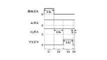
つづいて、成膜装置1における成膜処理の流れについて、図5を参照しながら説明する。図5は、実施形態に係る成膜処理の流れを示すタイミングチャートである。<Film film processing with a film forming device>
Next, the flow of the film forming process in the film forming apparatus 1 will be described with reference to FIG. FIG. 5 is a timing chart showing the flow of the film forming process according to the embodiment.
成膜装置1において成膜を行なうには、まずゲートバルブ28を開状態にして処理対象の半導体ウエハWをチャンバ10内に搬入して、サセプタ12または静電チャック40の上に載置する。静電チャック40に載置する場合、オン/オフ切替スイッチ44をオンにし、静電吸着力によって静電チャック40上に半導体ウエハWを吸着保持する。また、静電チャック40と半導体ウエハWとの間に伝熱ガスを供給する。 In order to perform film formation in the film forming apparatus 1, first, the
そして、図5に示すように、原料ガス供給部76より成膜原料ガスである原料ガスおよびパージガスを所定の流量でチャンバ10内に導入し、排気装置26によりチャンバ10内の圧力を設定値に調節する(ステップS1)。 Then, as shown in FIG. 5, the raw material gas and the purge gas, which are the film-forming raw material gas, are introduced into the
例えば、TiO2を成膜する場合、原料ガスとしては、テトラキスジメチルアミノチタン(TDMAT)ガスが好ましい。一方で、四塩化チタン(TiCl4)、テトラ(イソプロポキシ)チタン(TTIP)、四臭化チタン(TiBr4)、四ヨウ化チタン(TiI4)、テトラキスエチルメチルアミノチタン(TEMAT)等の他のTi含有ガスを用いることもできる。For example, when forming a TiO2 film, tetrakisdimethylaminotitanium (TDMAT) gas is preferable as the raw material gas. On the other hand, other titanium tetrachloride (TiCl4 ), tetra (isopropoxy) titanium (TTIP), titanium tetrabromide (TiBr4 ), titanium tetraiodide (TiI4), tetrakisethylmethylaminotitanium (TEMAT), etc. Ti-containing gas can also be used.
また、パージガスとしては、例えば、Arガス及びO2ガスの混合ガス(以下、Ar/O2ガスと呼ぶことがある)等が用いられる。Further, as the purge gas, for example, a mixed gas of Ar gas and O2 gas (hereinafter, may be referred to as Ar / O2 gas) or the like is used.
次に、原料ガスの供給を停止する(ステップS2)。これにより、Ar/O2ガスで半導体ウエハWの表面がパージされ、半導体ウエハWの表面に付着した余分な原料ガスの分子が除去される。Next, the supply of the raw material gas is stopped (step S2). As a result, the surface of the semiconductor wafer W is purged with Ar / O2 gas, and the excess raw material gas molecules adhering to the surface of the semiconductor wafer W are removed.
次に、高周波電源30及び可変直流電源80を用いて、所定の電圧を上部電極60,62に印加し、処理空間PSにプラズマを生成する(ステップS3)。上部電極60,62と下部電極として用いられるサセプタ12との間での放電によって酸素分子がプラズマ化し、このプラズマで生成される酸素ラジカルや酸素イオンと、半導体ウエハW表面に吸着した原料ガスの分子とが反応する。これにより、半導体ウエハW表面にTiO2の被膜が生成される。Next, using the high
次に、処理空間PS内のプラズマ生成を停止する(ステップS4)。これにより、Ar/O2ガスで半導体ウエハWの表面がパージされ、余分なTiO2の分子が除去される。これにより、原子層1層分のTiO2膜が形成される。そして、ここまで説明したステップS1~S4の処理を繰り返すことにより、所望の膜厚を有するTiO2膜を半導体ウエハWの表面に形成することができる。Next, plasma generation in the processing space PS is stopped (step S4). As a result, the surface of the semiconductor wafer W is purged with Ar / O2 gas, and excess TiO2 molecules are removed. As a result, a TiO2 film for one atomic layer is formed. Then, by repeating the processes of steps S1 to S4 described so far, a TiO2 film having a desired film thickness can be formed on the surface of the semiconductor wafer W.
例えば、図5に示すように、ステップS1を0.4秒行い、ステップS2を0.4秒行い、ステップS3を0.4秒行い、ステップS4を0.1秒行うことにより、半導体ウエハWの表面にTiO2膜を形成することができる。なお、ステップS1~S4の実施時間はかかる例に限られない。For example, as shown in FIG. 5, the semiconductor wafer W is performed by performing step S1 for 0.4 seconds, step S2 for 0.4 seconds, step S3 for 0.4 seconds, and step S4 for 0.1 seconds. A TiO2 film can be formed on the surface of the surface. The implementation time of steps S1 to S4 is not limited to such an example.
<実験結果>
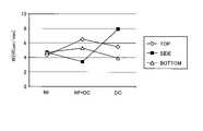
つづいて、成膜装置1を用いて様々な条件で成膜したTiO2膜の各種特性に関する実験結果について、図6~図10を参照しながら説明する。図6は、実施形態の各プラズマ生成条件において形成されたTiO2膜のトップ位置、サイド位置及びボトム位置におけるWER(Wet Etching Rate)を示した図である。<Experimental results>
Subsequently, the experimental results regarding various characteristics of the TiO2 film formed under various conditions using the film forming apparatus 1 will be described with reference to FIGS. 6 to 10. FIG. 6 is a diagram showing WER (Wet Etching Rate) at the top position, side position, and bottom position of the TiO2 film formed under each plasma generation condition of the embodiment.
この実験結果は、半導体ウエハW上に矩形状の凸部を複数並べて形成し、かかる凸部上にTiO2膜を形成した場合のWERを示している。また、かかるWERは、凸部の上面(以下、トップ位置と呼ぶことがある)と、凸部の側面(以下、サイド位置と呼ぶことがある)と、隣接する凸部間の底面(以下、ボトム位置と呼ぶことがある)とについてそれぞれ評価した。This experimental result shows WER in the case where a plurality of rectangular convex portions are formed side by side on the semiconductor wafer W and a TiO2 film is formed on the convex portions. Further, such a WER includes an upper surface of the convex portion (hereinafter, may be referred to as a top position), a side surface of the convex portion (hereinafter, may be referred to as a side position), and a bottom surface between adjacent convex portions (hereinafter, referred to as a side position). (Sometimes called the bottom position) was evaluated.
さらに、この実験結果におけるTiO2膜の成膜は、上述のステップS3の実施時間0.4秒、圧力0.5Torrで行い、インピーダンス調整回路100を動作させずに半導体ウエハWを接地させた状態で行った。Further, the film formation of the TiO2 film in this experimental result is performed in the above-mentioned step S3 with an implementation time of 0.4 seconds and a pressure of 0.5 Torr, and the semiconductor wafer W is grounded without operating the
そして、ステップS3におけるプラズマ生成を、上部電極60,62に高周波電圧(RF200W)を投入した場合と、重畳電圧(RF200W+DC330V)を投入した場合と、直流パルス電圧(DC410V)を投入した場合とで比較した。なお、高周波電圧の周波数は13.56MHzであり、DCパルス電圧の周波数は500kHz、デューティ比は50%である(以下同様)。 Then, the plasma generation in step S3 is compared between the case where the high frequency voltage (RF200W) is applied to the
図6に示すように、プラズマを高周波電圧(図では「RF」と記載)で生成することにより、トップ位置と、サイド位置と、ボトム位置とのWERを略均等に揃えることができる。すなわち、実施形態では、プラズマを高周波電圧で生成することにより、凹凸のある半導体ウエハWの表面にWERが略均等なTiO2膜を形成することができる。As shown in FIG. 6, by generating plasma with a high frequency voltage (denoted as “RF” in the figure), the WER of the top position, the side position, and the bottom position can be substantially evenly aligned. That is, in the embodiment, by generating plasma with a high frequency voltage, it is possible to form a TiO2 film having substantially uniform WER on the surface of the semiconductor wafer W having irregularities.
また、プラズマを重畳電圧(図では「RF+DC」と記載)で生成することにより、トップ位置及びボトム位置に比べて、サイド位置のWERを小さくすることができる。すなわち、実施形態では、プラズマを重畳電圧で生成することにより、ダブルパターニングプロセスのスペーサにTiO2膜を適用する場合に、マスクとして用いるサイド位置のTiO2膜をより残しやすくすることができる。Further, by generating plasma with a superposed voltage (described as "RF + DC" in the figure), the WER at the side position can be made smaller than that at the top position and the bottom position. That is, in the embodiment, by generating the plasma with the superimposed voltage, when the TiO2 film is applied to the spacer of the double patterning process, it is possible to make it easier to leave the TiO2 film at the side position used as a mask.
さらに、プラズマを直流パルス電圧(図では「DC」と記載)で生成することにより、トップ位置及びボトム位置に比べて、サイド位置のWERを大きくすることができる。すなわち、実施形態では、プラズマを直流パルス電圧で生成することにより、凹凸のある半導体ウエハWのトップ位置とボトム位置とに選択的にTiO2膜を形成する場合に、効率良くTiO2膜を形成することができる。Further, by generating plasma with a DC pulse voltage (denoted as "DC" in the figure), the WER at the side position can be made larger than that at the top position and the bottom position. That is, in the embodiment, when plasma is generated by a DC pulse voltage to selectively form a TiO2 film at the top position and the bottom position of the uneven semiconductor wafer W, the TiO2 film is efficiently formed. can do.
ここまで説明したように、実施形態によれば、上部電極60,62に投入される電圧を、切替部6で高周波電圧、重畳電圧または直流パルス電圧に切り替えることにより、同じ成膜装置1において成膜される薄膜のWERを多様に制御することができる。 As described above, according to the embodiment, the voltage applied to the
なお、投入される電圧の種類で薄膜のWERが大きく変化するのは、プラズマ中のイオンやラジカルの入射分布およびフラックスが、水平面(=トップ位置やボトム位置)と垂直面(=サイド位置)とにおいて投入される電圧の種類により大きく変わることが要因と推測される。 The reason why the WER of the thin film changes greatly depending on the type of voltage applied is that the incident distribution and flux of ions and radicals in the plasma are on the horizontal plane (= top position and bottom position) and the vertical plane (= side position). It is presumed that the factor is that it changes greatly depending on the type of voltage applied in.
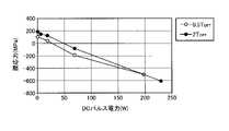
図7は、実施形態の重畳電圧におけるDCパルス電力と膜応力との関係を示した図(1)である。この実験結果は、平坦な半導体ウエハW上にTiO2膜を形成した場合の膜応力を示している。なお、かかるTiO2膜の膜応力は、ダブルパターニングプロセスのスペーサにTiO2膜を適用する場合の重要なパラメータである。FIG. 7 is a diagram (1) showing the relationship between the DC pulse power and the film stress at the superimposed voltage of the embodiment. This experimental result shows the film stress when the TiO2 film is formed on the flat semiconductor wafer W. The film stress of the TiO2 film is an important parameter when the TiO2 film is applied to the spacer of the double patterning process.
この実験結果におけるTiO2膜の成膜は、ステップS3の実施時間0.4秒、圧力0.5Torr及び2Torrで行い、インピーダンス調整回路100を動作させずに半導体ウエハWを接地させた状態で行った。そして、重畳電圧をRF200W一定で、DCパルス電圧を様々に変化させて上部電極60,62に印加してプラズマ生成を行い、かかる変化させた各直流パルス電圧での膜応力をプロットした。The film formation of the TiO2 film in this experimental result was performed with the implementation time of step S3 of 0.4 seconds, the pressures of 0.5 Torr and 2 Torr, and the semiconductor wafer W was grounded without operating the
図7に示すように、圧力が2Torrの場合で、直流パルス電力をゼロ、すなわちプラズマを高周波電圧で生成することにより、膜応力をtensile(プラス側)にすることができる。一方で、同じ条件で直流パルス電力を印加、すなわちプラズマを重畳電圧で生成することにより、膜応力をcompressive(マイナス側)にすることができる。 As shown in FIG. 7, when the pressure is 2 Torr, the DC pulse power is zero, that is, the plasma is generated at a high frequency voltage, so that the film stress can be set to tensile (plus side). On the other hand, the film stress can be made compressive (minus side) by applying DC pulse power under the same conditions, that is, by generating plasma with a superposed voltage.
このように、実施形態によれば、上部電極60,62に投入される電圧を、切替部6で高周波電圧または重畳電圧に切り替えることにより、同じ成膜装置1において成膜される薄膜の膜応力を多様に制御することができる。 As described above, according to the embodiment, the film stress of the thin film formed in the same film forming apparatus 1 by switching the voltage applied to the
図8は、実施形態の重畳電圧におけるDCパルス電力と膜応力との関係を示した図(2)である。この実験結果は、インピーダンス調整回路100を動作させて半導体ウエハWをフローティング状態にした以外は図7の実験結果と同じ条件でTiO2膜を成膜した場合の結果である。FIG. 8 is a diagram (2) showing the relationship between the DC pulse power and the film stress at the superimposed voltage of the embodiment. This experimental result is the result when the TiO2 film is formed under the same conditions as the experimental result of FIG. 7 except that the
図8に示すように、直流パルス電力をゼロ、すなわちプラズマを高周波電圧で生成することにより、いずれの圧力でも図7の例に比べて膜応力をよりtensile(プラス側)にすることができる。さらに、同じ条件で直流パルス電力を印加、すなわちプラズマを重畳電圧で生成することにより、膜応力を段階的にcompressive(マイナス側)に制御することができる。 As shown in FIG. 8, by generating zero DC pulse power, that is, plasma at a high frequency voltage, the film stress can be made more tensile (plus side) than in the example of FIG. 7 at any pressure. Further, by applying DC pulse power under the same conditions, that is, by generating plasma with a superposed voltage, the film stress can be controlled stepwise to compressive (minus side).
このように、実施形態によれば、インピーダンス調整回路100を動作させることにより、同じ成膜装置1において成膜される薄膜の膜応力をさらに多様に制御することができる。 As described above, according to the embodiment, by operating the
図9は、実施形態の各プラズマ生成条件において形成されたTiO2膜の屈折率を示した図である。この実験結果は、平坦な半導体ウエハW上にTiO2膜を形成した場合の屈折率を示している。FIG. 9 is a diagram showing the refractive index of the TiO2 film formed under each plasma generation condition of the embodiment. This experimental result shows the refractive index when the TiO2 film is formed on the flat semiconductor wafer W.
また、この実験結果におけるTiO2膜の成膜は、ステップS3の実施時間0.4秒、圧力0.5Torr及び2Torrで行い、インピーダンス調整回路100を動作させずに半導体ウエハWを接地させた状態で行った。Further, the film formation of the TiO2 film in this experimental result was performed with the implementation time of step S3 of 0.4 seconds, the pressures of 0.5 Torr and 2 Torr, and the semiconductor wafer W was grounded without operating the
そして、ステップS3におけるプラズマ生成を、上部電極60,62に高周波電圧(RF200W)を投入した場合と、重畳電圧(RF200W+DC330V)を投入した場合と、直流パルス電圧(DC410V)を投入した場合とで比較した。 Then, the plasma generation in step S3 is compared between the case where the high frequency voltage (RF200W) is applied to the
図9に示すように、投入される電圧の種類及び圧力を変えてプラズマを生成することにより、波長633nmにおけるTiO2膜の屈折率を2.23から2.39まで様々に制御することができる。As shown in FIG. 9, the refractive index of the TiO2 film at a wavelength of 633 nm can be variously controlled from 2.23 to 2.39 by generating plasma by changing the type and pressure of the applied voltage. ..
このように、実施形態によれば、上部電極60,62に投入される電圧を、切替部6で高周波電圧、重畳電圧または直流パルス電圧に切り替えることにより、同じ成膜装置1において成膜される薄膜の屈折率を多様に制御することができる。 As described above, according to the embodiment, the voltage applied to the
図10は、実施形態の各プラズマ生成条件において形成された膜の均一性を示した図であり、図9に示した例と同じ条件で半導体ウエハW上にTiO2膜を形成した場合の均一性を1σの値で示している。FIG. 10 is a diagram showing the uniformity of the film formed under each plasma generation condition of the embodiment, and is the uniformity when the TiO2 film is formed on the semiconductor wafer W under the same conditions as the example shown in FIG. The sex is indicated by a value of 1σ.
図10に示すように、圧力が2Torrの場合で、プラズマを重畳電圧または直流パルス電圧で生成することにより、プラズマを高周波電圧で生成する場合に比べて膜の均一性を向上させることができる。また、圧力が0.5Torrの場合でも、プラズマを直流パルス電圧で生成することにより、プラズマを高周波電圧で生成する場合に比べて膜の均一性を向上させることができる。 As shown in FIG. 10, when the pressure is 2 Torr, the uniformity of the film can be improved by generating the plasma with a superposed voltage or a DC pulse voltage as compared with the case where the plasma is generated with a high frequency voltage. Further, even when the pressure is 0.5 Torr, by generating the plasma with a DC pulse voltage, the uniformity of the film can be improved as compared with the case where the plasma is generated with a high frequency voltage.
<一定の直流電圧の適用について>
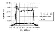
つづいて、高周波電圧との重畳電圧にパルス状の直流電圧(すなわち、直流パルス電圧)を適用した場合と、一定の直流電圧を適用した場合との比較について、図11及び図12を参照しながら説明する。<Application of constant DC voltage>
Next, with reference to FIGS. 11 and 12, a comparison between the case where a pulsed DC voltage (that is, the DC pulse voltage) is applied to the superimposed voltage with the high frequency voltage and the case where a constant DC voltage is applied is compared. explain.
上述のように、可変直流電源80に接続されたパルス発生器84は、パルス状のほかに一定の直流電圧を出力することもできることから、高周波電圧との重畳電圧に一定の直流電圧を適用することができる。そこで、高周波電圧との重畳電圧に一定の直流電圧を適用した場合と、直流パルス電圧を適用した場合との効果の違いについて以下に検証する。 As described above, since the pulse generator 84 connected to the variable
図11は、高周波電圧との重畳電圧に一定の直流電圧を適用した場合とパルス状の直流電圧を適用した場合との電子密度を示した図(1)である。具体的には、図11は、かかる両方の場合において、直流電力を300Wで一定にして高周波電力を変化させた際の電子密度をプラズマ計測で評価した結果について示している。なお、図11及び図12には、理解の容易のため、高周波電圧のみを印加した場合のプラズマ計測結果も示している。 FIG. 11 is a diagram (1) showing the electron densities when a constant DC voltage is applied to the superimposed voltage with the high frequency voltage and when a pulsed DC voltage is applied. Specifically, FIG. 11 shows the results of plasma measurement evaluation of the electron density when the DC power is kept constant at 300 W and the high frequency power is changed in both of these cases. Note that FIGS. 11 and 12 also show plasma measurement results when only a high frequency voltage is applied for easy understanding.
図11に示すように、高周波電圧のみを印加した場合に比べて、高周波電圧との重畳電圧にパルス状の直流電圧を適用することにより、プラズマ中の電子密度を大きく増加させることができる。さらに、高周波電圧との重畳電圧に一定の直流電圧を適用した場合にも、パルス状の直流電圧を適用した場合と同等の電子密度を増加させる効果を得ることができる。 As shown in FIG. 11, the electron density in the plasma can be greatly increased by applying the pulsed DC voltage to the superimposed voltage with the high frequency voltage as compared with the case where only the high frequency voltage is applied. Further, even when a constant DC voltage is applied to the superimposed voltage with the high frequency voltage, the effect of increasing the electron density equivalent to that when the pulsed DC voltage is applied can be obtained.
図12は、高周波電圧との重畳電圧に一定の直流電圧を適用した場合とパルス状の直流電圧を適用した場合との電子密度を示した図(2)であり、かかる両方の場合における電子密度の面内分布について示している。 FIG. 12 is a diagram (2) showing the electron density when a constant DC voltage is applied to the superposed voltage with the high frequency voltage and when a pulsed DC voltage is applied, and the electron density in both cases is shown. The in-plane distribution of is shown.
図12に示すように、高周波電圧との重畳電圧に一定の直流電圧を適用した場合にも、パルス状の直流電圧を適用した場合と同等の面内分布を得ることができる。 As shown in FIG. 12, even when a constant DC voltage is applied to the superimposed voltage with the high frequency voltage, the same in-plane distribution as when the pulsed DC voltage is applied can be obtained.
このように、実施形態では、高周波電圧との重畳電圧に一定の直流電圧を適用した場合に、直流パルス電圧を適用した場合と同等の効果を得ることができる。したがって、実施形態によれば、高周波電圧との重畳電圧に一定の直流電圧を適用することにより、同じ成膜装置において成膜される薄膜の膜質を多様に制御することができる。 As described above, in the embodiment, when a constant DC voltage is applied to the superimposed voltage with the high frequency voltage, the same effect as when the DC pulse voltage is applied can be obtained. Therefore, according to the embodiment, by applying a constant DC voltage to the superimposed voltage with the high frequency voltage, it is possible to control the film quality of the thin film formed in the same film forming apparatus in various ways.
また、高周波電圧との重畳電圧に一定の直流電圧を適用することにより、電圧印加部5のパルス発生器84を不要にすることができることから、成膜装置1の製造コストを低減することができる。 Further, by applying a constant DC voltage to the superposed voltage with the high frequency voltage, the pulse generator 84 of the voltage applying unit 5 can be eliminated, so that the manufacturing cost of the film forming apparatus 1 can be reduced. ..
以上のように、実施形態では、成膜装置1は、真空排気可能なチャンバ10と、下部電極として用いられるサセプタ12、上部電極60,62と、原料ガス供給部76と、電圧印加部5と、切替部6とを有する。サセプタ12には被処理基板が載置される。上部電極60,62は、チャンバ10内でサセプタ12に対向して配置される。原料ガス供給部76は、上部電極60,62とサセプタ12との間の処理空間PSでプラズマ化する成膜原料ガスを処理空間PSに供給する。電圧印加部5は、高周波電源30及び可変直流電源80を有し、高周波電源30及び可変直流電源80のうち少なくとも一方から出力される電圧を上部電極60,62に印加する。切替部6は、上部電極60,62に印加される電圧を、高周波電源30から出力される高周波電圧と、可変直流電源80から出力される直流電圧と、高周波電圧に直流電圧が重畳された重畳電圧とで切り替える。 As described above, in the embodiment, the film forming apparatus 1 includes a
こうすることで、同じ成膜装置1において成膜される薄膜の膜質を多様に制御することができる。 By doing so, it is possible to control the film quality of the thin film formed in the same film forming apparatus 1 in various ways.
また、実施形態では、成膜装置1は、サセプタ12と接地との間に接続されたインピーダンス調整回路100を有する。こうすることで、同じ成膜装置1において成膜される薄膜の膜応力をさらに多様に制御することができる。 Further, in the embodiment, the film forming apparatus 1 has an
また、実施形態では、可変直流電源80から出力される直流電圧はパルス状である。こうすることで、半導体ウエハW上に形成される膜の均一性を向上させることができる。 Further, in the embodiment, the DC voltage output from the variable
また、実施形態では、可変直流電源80から出力される直流電圧は一定である。こうすることで、成膜装置1の製造コストを低減することができる。 Further, in the embodiment, the DC voltage output from the variable
以上、本開示の実施形態について説明したが、本開示は上記実施形態に限定されるものではなく、その趣旨を逸脱しない限りにおいて種々の変更が可能である。たとえば、上記の実施形態では、ステップS1~S4の処理を繰り返して1層の膜を成膜する際には、投入される電圧の種類を固定して成膜した例について示したが、ステップS1~S4の処理を繰り返す際に投入される電圧の種類を適宜変更してもよい。 Although the embodiments of the present disclosure have been described above, the present disclosure is not limited to the above-described embodiments, and various changes can be made without departing from the spirit of the present disclosure. For example, in the above embodiment, when the process of steps S1 to S4 is repeated to form a one-layer film, an example in which the type of applied voltage is fixed to form a film is shown, but step S1 is shown. The type of voltage applied when the processing of to S4 is repeated may be appropriately changed.
例えば、成膜処理の前半では高周波電圧でプラズマ生成して膜応力がtensileな膜を成膜し、成膜処理の後半では重畳電圧でプラズマ生成して膜応力がcompressiveな膜を成膜してもよい。これにより、膜応力を全体としてゼロに近づけることができる。 For example, in the first half of the film formation process, plasma is generated at a high frequency voltage to form a film with a tense film stress, and in the second half of the film formation process, plasma is generated at a superposed voltage to form a film with a pressure film stress. May be good. As a result, the film stress can be brought close to zero as a whole.
なお、本開示の実施形態はすべての点で例示であって制限的なものではないと考えられるべきである。実に、上記の実施形態は多様な形態で具現され得る。また、上記の実施形態は、特許請求の範囲及びその趣旨を逸脱することなく、様々な形態で省略、置換、変更されても良い。 It should be noted that the embodiments of the present disclosure are exemplary in all respects and are not restrictive. Indeed, the above embodiments can be embodied in a variety of forms. Further, the above-described embodiment may be omitted, replaced or changed in various forms without departing from the scope of claims and the purpose thereof.
W 半導体ウエハ(被処理基板の一例)
1 成膜装置
5 電圧印加部
6 切替部
10 チャンバ
12 サセプタ(下部電極の一例)
30 高周波電源
60,62 上部電極
76 原料ガス供給部
80 可変直流電源(直流電源の一例)
100 インピーダンス調整回路
PS 処理空間W Semiconductor wafer (an example of a substrate to be processed)
1 Film forming device 5
30 High
100 Impedance adjustment circuit PS processing space
Claims (7)
Translated fromJapanese前記処理容器内で被処理基板が載置される下部電極と、
前記処理容器内で前記下部電極に対向して配置される上部電極と、
前記上部電極と前記下部電極との間の処理空間でプラズマ化する成膜原料ガスを前記処理空間に供給するガス供給部と、
高周波電源及び直流電源を有し、前記高周波電源及び前記直流電源のうち少なくとも一方から出力される電圧を前記上部電極に印加する電圧印加部と、
前記上部電極に印加される電圧を、前記高周波電源から出力される高周波電圧と、前記直流電源から出力される直流電圧と、前記高周波電圧に前記直流電圧が重畳された重畳電圧とで切り替える切替部と、
各部を制御する制御部と、
を具備し、
前記制御部は、前記成膜原料ガスを前記高周波電圧でプラズマ化することで、成膜される薄膜の膜応力をtensileにし、前記成膜原料ガスを前記重畳電圧でプラズマ化することで、成膜される薄膜の膜応力をcompressiveにする
成膜装置。A processing container that can be evacuated and
The lower electrode on which the substrate to be processed is placed in the processing container,
An upper electrode arranged in the processing container facing the lower electrode, and an upper electrode.
A gas supply unit that supplies the film-forming raw material gas that is turned into plasma in the processing space between the upper electrode and the lower electrode to the processing space,
A voltage application unit having a high frequency power supply and a DC power supply and applying a voltage output from at least one of the high frequency power supply and the DC power supply to the upper electrode.
A switching unit that switches the voltage applied to the upper electrode between a high frequency voltage output from the high frequency power supply, a DC voltage output from the DC power supply, and a superposed voltage in which the DC voltage is superimposed on the high frequency voltage. When,
A control unit that controls each unit,
Equippedwith
The control unit is formed by converting the film-forming raw material gas into plasma at the high-frequency voltage to make the film stress of the thin film to be filmed tendle, and to plasma-form the film-forming raw material gas at the superimposed voltage. Make the film stress of the thin film to be filmed compressive
Film forming equipment.
をさらに具備する請求項1に記載の成膜装置。An impedance adjustment circuit connected between the lower electrode and ground,
The film forming apparatus according to claim 1, further comprising.
請求項1または2に記載の成膜装置。The DC voltage output from the DC power supply is pulsed.
The film forming apparatus according to claim 1 or 2.
請求項1または2に記載の成膜装置。The DC voltage output from the DC power supply is constant.
The film forming apparatus according to claim 1 or 2.
前記処理容器内で被処理基板が載置される下部電極と、The lower electrode on which the substrate to be processed is placed in the processing container,
前記処理容器内で前記下部電極に対向して配置される上部電極と、An upper electrode arranged in the processing container facing the lower electrode, and an upper electrode.
成膜原料ガスを前記処理容器に供給するガス供給部と、A gas supply unit that supplies the film-forming raw material gas to the processing container,
前記上部電極に高周波電圧を印加する高周波電源と、A high-frequency power supply that applies a high-frequency voltage to the upper electrode,
前記上部電極に直流電圧を印加する直流電源と、を有し、It has a DC power supply that applies a DC voltage to the upper electrode.
前記処理容器内にプラズマを生成し、前記成膜原料ガスをプラズマ化して前記被処理基板の表面に成膜処理を行う成膜装置によって行われる成膜方法において、In a film forming method performed by a film forming apparatus that generates plasma in the processing container, turns the film forming raw material gas into plasma, and performs a film forming process on the surface of the substrate to be processed.
前記成膜原料ガスを前記高周波電圧でプラズマ化することで、成膜される薄膜の膜応力をtensileにし、前記成膜原料ガスを前記高周波電圧に前記直流電圧が重畳された重畳電圧でプラズマ化することで、成膜される薄膜の膜応力をcompressiveにするBy converting the film-forming raw material gas into plasma at the high-frequency voltage, the film stress of the film-formed thin film is made tensile, and the film-forming raw material gas is converted into plasma at the superimposed voltage in which the DC voltage is superimposed on the high-frequency voltage. By doing so, the film stress of the thin film to be formed is made compact.
成膜方法。Film formation method.
請求項5に記載の成膜方法。The film forming method according to claim 5.
請求項5に記載の成膜方法。The film forming method according to claim 5.
Priority Applications (6)
| Application Number | Priority Date | Filing Date | Title |
|---|---|---|---|
| JP2018112585AJP7094154B2 (en) | 2018-06-13 | 2018-06-13 | Film forming equipment and film forming method |
| US16/431,565US20190385815A1 (en) | 2018-06-13 | 2019-06-04 | Film forming apparatus |
| KR1020190069236AKR102202347B1 (en) | 2018-06-13 | 2019-06-12 | Film forming apparatus |
| CN201910505338.5ACN110592558B (en) | 2018-06-13 | 2019-06-12 | Film forming apparatus |
| KR1020200178706AKR102244353B1 (en) | 2018-06-13 | 2020-12-18 | Film forming method |
| US17/974,193US12027344B2 (en) | 2018-06-13 | 2022-10-26 | Film forming apparatus |
Applications Claiming Priority (1)
| Application Number | Priority Date | Filing Date | Title |
|---|---|---|---|
| JP2018112585AJP7094154B2 (en) | 2018-06-13 | 2018-06-13 | Film forming equipment and film forming method |
Publications (2)
| Publication Number | Publication Date |
|---|---|
| JP2019216182A JP2019216182A (en) | 2019-12-19 |
| JP7094154B2true JP7094154B2 (en) | 2022-07-01 |
Family
ID=68840228
Family Applications (1)
| Application Number | Title | Priority Date | Filing Date |
|---|---|---|---|
| JP2018112585AActiveJP7094154B2 (en) | 2018-06-13 | 2018-06-13 | Film forming equipment and film forming method |
Country Status (4)
| Country | Link |
|---|---|
| US (2) | US20190385815A1 (en) |
| JP (1) | JP7094154B2 (en) |
| KR (2) | KR102202347B1 (en) |
| CN (1) | CN110592558B (en) |
Families Citing this family (7)
| Publication number | Priority date | Publication date | Assignee | Title |
|---|---|---|---|---|
| WO2021020723A1 (en)* | 2019-07-26 | 2021-02-04 | 주성엔지니어링(주) | Substrate processing apparatus, and method for interlocking of same |
| JP7482657B2 (en)* | 2020-03-17 | 2024-05-14 | 東京エレクトロン株式会社 | CLEANING METHOD AND SEMICONDUCTOR DEVICE MANUFACTURING METHOD |
| JP7689417B2 (en)* | 2020-07-10 | 2025-06-06 | 東京エレクトロン株式会社 | Film forming apparatus and film forming method |
| JP2022110695A (en)* | 2021-01-19 | 2022-07-29 | 東京エレクトロン株式会社 | Plasma processing method and plasma processing apparatus |
| CN113564552A (en)* | 2021-07-29 | 2021-10-29 | 中国科学院兰州化学物理研究所 | Electromagnetic separation type coating device and method |
| JP2023055111A (en)* | 2021-10-05 | 2023-04-17 | 東京エレクトロン株式会社 | Method and device for forming titanium film |
| KR20240128193A (en)* | 2023-02-17 | 2024-08-26 | 피에스케이 주식회사 | Substrate processing apparatus and method |
Citations (2)
| Publication number | Priority date | Publication date | Assignee | Title |
|---|---|---|---|---|
| JP2004158247A (en) | 2002-11-05 | 2004-06-03 | Sharp Corp | Plasma processing apparatus and plasma processing method |
| JP2008305856A (en) | 2007-06-05 | 2008-12-18 | Tokyo Electron Ltd | Plasma processing apparatus, electrode temperature adjusting apparatus, electrode temperature adjusting method |
Family Cites Families (38)
| Publication number | Priority date | Publication date | Assignee | Title |
|---|---|---|---|---|
| CA1007308A (en)* | 1972-12-29 | 1977-03-22 | Jack A. Dorler | Cross-coupled capacitor for ac performance tuning |
| KR910000273B1 (en) | 1985-05-09 | 1991-01-23 | 마쯔시다덴기산교 가부시기가이샤 | Plasma processor |
| JPH08181118A (en) | 1994-12-26 | 1996-07-12 | Nissin Electric Co Ltd | Plasma processor |
| JPH1131685A (en) | 1997-07-14 | 1999-02-02 | Hitachi Electron Eng Co Ltd | Plasma CVD apparatus and cleaning method therefor |
| JP2002217278A (en) | 2001-01-12 | 2002-08-02 | Mitsubishi Heavy Ind Ltd | Plasma cvd device |
| JP2003166047A (en)* | 2001-09-20 | 2003-06-13 | Shin Meiwa Ind Co Ltd | Halogen compound film forming method and film forming apparatus, and magnesium fluoride film |
| TWI574318B (en)* | 2004-06-21 | 2017-03-11 | Tokyo Electron Ltd | A plasma processing apparatus, a plasma processing method, and a computer-readable recording medium |
| US7988816B2 (en) | 2004-06-21 | 2011-08-02 | Tokyo Electron Limited | Plasma processing apparatus and method |
| US20060037704A1 (en) | 2004-07-30 | 2006-02-23 | Tokyo Electron Limited | Plasma Processing apparatus and method |
| US7692916B2 (en) | 2005-03-31 | 2010-04-06 | Tokyo Electron Limited | Capacitive coupling plasma processing apparatus and method |
| KR100975268B1 (en) | 2005-11-18 | 2010-08-11 | 가부시키가이샤 히다치 고쿠사이 덴키 | Method of manufacturing semiconductor device and substrate processing apparatus |
| US20080053817A1 (en)* | 2006-09-04 | 2008-03-06 | Tokyo Electron Limited | Plasma processing apparatus and plasma processing method |
| KR20080111627A (en) | 2007-06-19 | 2008-12-24 | 삼성전자주식회사 | Plasma processing apparatus and method thereof |
| JP4607930B2 (en) | 2007-09-14 | 2011-01-05 | 株式会社東芝 | Plasma processing apparatus and plasma processing method |
| JP5224837B2 (en) | 2008-02-01 | 2013-07-03 | 株式会社東芝 | Substrate plasma processing apparatus and plasma processing method |
| JP2009239012A (en) | 2008-03-27 | 2009-10-15 | Tokyo Electron Ltd | Plasma processing device and method of plasma etching |
| JP2010238881A (en) | 2009-03-31 | 2010-10-21 | Tokyo Electron Ltd | Plasma processing apparatus and plasma processing method |
| JP2011023718A (en) | 2009-07-15 | 2011-02-03 | Asm Japan Kk | METHOD FOR FORMING STRESS-TUNED DIELECTRIC FILM HAVING Si-N BOND BY PEALD |
| JP5571996B2 (en)* | 2010-03-31 | 2014-08-13 | 東京エレクトロン株式会社 | Plasma processing method and plasma processing apparatus |
| KR20120022251A (en) | 2010-09-01 | 2012-03-12 | 삼성전자주식회사 | Plasma etching method and apparatus thereof |
| JP5864879B2 (en) | 2011-03-31 | 2016-02-17 | 東京エレクトロン株式会社 | Substrate processing apparatus and control method thereof |
| US9373517B2 (en) | 2012-08-02 | 2016-06-21 | Applied Materials, Inc. | Semiconductor processing with DC assisted RF power for improved control |
| JP6202098B2 (en)* | 2013-09-10 | 2017-09-27 | 株式会社島津製作所 | Film forming apparatus and film forming method |
| US9556516B2 (en)* | 2013-10-09 | 2017-01-31 | ASM IP Holding B.V | Method for forming Ti-containing film by PEALD using TDMAT or TDEAT |
| JP6320248B2 (en) | 2014-03-04 | 2018-05-09 | 東京エレクトロン株式会社 | Plasma etching method |
| WO2015141521A1 (en) | 2014-03-21 | 2015-09-24 | 株式会社日立国際電気 | Substrate processing apparatus, semiconductor device manufacturing method, and recording medium |
| KR20160028612A (en) | 2014-09-03 | 2016-03-14 | 삼성전자주식회사 | Semiconductor fabricating apparatus and method of fabricating semiconductor device using the same |
| TWI737612B (en)* | 2015-06-18 | 2021-09-01 | 美商應用材料股份有限公司 | Deposition methods for uniform and conformal hybrid titanium oxide films |
| JP6114370B2 (en) | 2015-12-24 | 2017-04-12 | 東京エレクトロン株式会社 | Substrate processing apparatus and control method thereof |
| JP6643950B2 (en)* | 2016-05-23 | 2020-02-12 | 東京エレクトロン株式会社 | Plasma processing method |
| US10515822B2 (en) | 2016-06-20 | 2019-12-24 | Taiwan Semiconductor Manufacturing Co., Ltd. | Method for preventing bottom layer wrinkling in a semiconductor device |
| JP6796431B2 (en)* | 2016-08-12 | 2020-12-09 | 東京エレクトロン株式会社 | Film forming equipment and gas discharge members used for it |
| JP6446418B2 (en) | 2016-09-13 | 2018-12-26 | 株式会社Kokusai Electric | Semiconductor device manufacturing method, substrate processing apparatus, and program |
| JP6815158B2 (en)* | 2016-10-13 | 2021-01-20 | 東京エレクトロン株式会社 | Titanium oxide film forming method and hard mask forming method |
| US10629415B2 (en) | 2017-03-28 | 2020-04-21 | Asm Ip Holding B.V. | Substrate processing apparatus and method for processing substrate |
| KR20190014623A (en) | 2017-08-03 | 2019-02-13 | 삼성전자주식회사 | Plasma processing apparatus and method of manufacturing a semiconductor device using the same |
| US10170300B1 (en)* | 2017-11-30 | 2019-01-01 | Tokyo Electron Limited | Protective film forming method |
| JP2020178099A (en) | 2019-04-22 | 2020-10-29 | 東京エレクトロン株式会社 | Matching method and plasma processing apparatus |
- 2018
- 2018-06-13JPJP2018112585Apatent/JP7094154B2/enactiveActive
- 2019
- 2019-06-04USUS16/431,565patent/US20190385815A1/ennot_activeAbandoned
- 2019-06-12KRKR1020190069236Apatent/KR102202347B1/enactiveActive
- 2019-06-12CNCN201910505338.5Apatent/CN110592558B/enactiveActive
- 2020
- 2020-12-18KRKR1020200178706Apatent/KR102244353B1/enactiveActive
- 2022
- 2022-10-26USUS17/974,193patent/US12027344B2/enactiveActive
Patent Citations (2)
| Publication number | Priority date | Publication date | Assignee | Title |
|---|---|---|---|---|
| JP2004158247A (en) | 2002-11-05 | 2004-06-03 | Sharp Corp | Plasma processing apparatus and plasma processing method |
| JP2008305856A (en) | 2007-06-05 | 2008-12-18 | Tokyo Electron Ltd | Plasma processing apparatus, electrode temperature adjusting apparatus, electrode temperature adjusting method |
Also Published As
| Publication number | Publication date |
|---|---|
| US12027344B2 (en) | 2024-07-02 |
| JP2019216182A (en) | 2019-12-19 |
| KR20200144531A (en) | 2020-12-29 |
| US20230051432A1 (en) | 2023-02-16 |
| KR102202347B1 (en) | 2021-01-12 |
| KR102244353B1 (en) | 2021-04-23 |
| CN110592558B (en) | 2022-10-18 |
| CN110592558A (en) | 2019-12-20 |
| KR20190141091A (en) | 2019-12-23 |
| US20190385815A1 (en) | 2019-12-19 |
Similar Documents
| Publication | Publication Date | Title |
|---|---|---|
| JP7094154B2 (en) | Film forming equipment and film forming method | |
| JP7038614B2 (en) | Board processing method | |
| US20210217591A1 (en) | Process chamber for cyclic and selective material removal and etching | |
| WO2019239872A1 (en) | Film-forming apparatus, and method for cleaning film-forming apparatus | |
| TWI544546B (en) | Plasma processing device and plasma processing method | |
| TWI469212B (en) | Plasma etching method | |
| TWI607484B (en) | Plasma processing method and plasma processing device | |
| US9502219B2 (en) | Plasma processing method | |
| CN111373511B (en) | Plasma processing method | |
| KR102586592B1 (en) | High Temperature RF Heater Pedestals | |
| JP2021523558A (en) | High quality C film pulsed plasma (DC / RF) deposition for patterning | |
| JP4935149B2 (en) | Electrode plate for plasma processing and plasma processing apparatus | |
| KR20150075362A (en) | Method of forming contact layer | |
| KR20150075363A (en) | METHOD OF FORMING Ti FILM | |
| TW202012699A (en) | Film forming device and film forming method | |
| JP5695117B2 (en) | Plasma etching method | |
| KR101088969B1 (en) | Plasma processing apparatus and plasma etching method | |
| US20240194446A1 (en) | Chamber impedance management in a processing chamber | |
| JP4350686B2 (en) | Method and apparatus for producing metal nitride film | |
| WO2021065497A1 (en) | Substrate processing device and substrate processing method |
Legal Events
| Date | Code | Title | Description |
|---|---|---|---|
| A621 | Written request for application examination | Free format text:JAPANESE INTERMEDIATE CODE: A621 Effective date:20210303 | |
| A977 | Report on retrieval | Free format text:JAPANESE INTERMEDIATE CODE: A971007 Effective date:20220112 | |
| A131 | Notification of reasons for refusal | Free format text:JAPANESE INTERMEDIATE CODE: A131 Effective date:20220118 | |
| A521 | Request for written amendment filed | Free format text:JAPANESE INTERMEDIATE CODE: A523 Effective date:20220318 | |
| TRDD | Decision of grant or rejection written | ||
| A01 | Written decision to grant a patent or to grant a registration (utility model) | Free format text:JAPANESE INTERMEDIATE CODE: A01 Effective date:20220524 | |
| A61 | First payment of annual fees (during grant procedure) | Free format text:JAPANESE INTERMEDIATE CODE: A61 Effective date:20220621 | |
| R150 | Certificate of patent or registration of utility model | Ref document number:7094154 Country of ref document:JP Free format text:JAPANESE INTERMEDIATE CODE: R150 | |
| R250 | Receipt of annual fees | Free format text:JAPANESE INTERMEDIATE CODE: R250 |