JP7083881B2 - Semiconductor device - Google Patents
Semiconductor deviceDownload PDFInfo
- Publication number
- JP7083881B2 JP7083881B2JP2020178939AJP2020178939AJP7083881B2JP 7083881 B2JP7083881 B2JP 7083881B2JP 2020178939 AJP2020178939 AJP 2020178939AJP 2020178939 AJP2020178939 AJP 2020178939AJP 7083881 B2JP7083881 B2JP 7083881B2
- Authority
- JP
- Japan
- Prior art keywords
- transistor
- region
- oxide semiconductor
- oxide
- wiring
- Prior art date
- Legal status (The legal status is an assumption and is not a legal conclusion. Google has not performed a legal analysis and makes no representation as to the accuracy of the status listed.)
- Active
Links
Images


Classifications
- H—ELECTRICITY
- H10—SEMICONDUCTOR DEVICES; ELECTRIC SOLID-STATE DEVICES NOT OTHERWISE PROVIDED FOR
- H10D—INORGANIC ELECTRIC SEMICONDUCTOR DEVICES
- H10D30/00—Field-effect transistors [FET]
- H10D30/60—Insulated-gate field-effect transistors [IGFET]
- H10D30/67—Thin-film transistors [TFT]
- H10D30/674—Thin-film transistors [TFT] characterised by the active materials
- H10D30/6755—Oxide semiconductors, e.g. zinc oxide, copper aluminium oxide or cadmium stannate
- G—PHYSICS
- G11—INFORMATION STORAGE
- G11C—STATIC STORES
- G11C11/00—Digital stores characterised by the use of particular electric or magnetic storage elements; Storage elements therefor
- G11C11/21—Digital stores characterised by the use of particular electric or magnetic storage elements; Storage elements therefor using electric elements
- G11C11/34—Digital stores characterised by the use of particular electric or magnetic storage elements; Storage elements therefor using electric elements using semiconductor devices
- G11C11/40—Digital stores characterised by the use of particular electric or magnetic storage elements; Storage elements therefor using electric elements using semiconductor devices using transistors
- G11C11/401—Digital stores characterised by the use of particular electric or magnetic storage elements; Storage elements therefor using electric elements using semiconductor devices using transistors forming cells needing refreshing or charge regeneration, i.e. dynamic cells
- G11C11/403—Digital stores characterised by the use of particular electric or magnetic storage elements; Storage elements therefor using electric elements using semiconductor devices using transistors forming cells needing refreshing or charge regeneration, i.e. dynamic cells with charge regeneration common to a multiplicity of memory cells, i.e. external refresh
- H—ELECTRICITY
- H10—SEMICONDUCTOR DEVICES; ELECTRIC SOLID-STATE DEVICES NOT OTHERWISE PROVIDED FOR
- H10B—ELECTRONIC MEMORY DEVICES
- H10B10/00—Static random access memory [SRAM] devices
- H10B10/12—Static random access memory [SRAM] devices comprising a MOSFET load element
- H10B10/125—Static random access memory [SRAM] devices comprising a MOSFET load element the MOSFET being a thin film transistor [TFT]
- H—ELECTRICITY
- H10—SEMICONDUCTOR DEVICES; ELECTRIC SOLID-STATE DEVICES NOT OTHERWISE PROVIDED FOR
- H10B—ELECTRONIC MEMORY DEVICES
- H10B12/00—Dynamic random access memory [DRAM] devices
- H10B12/01—Manufacture or treatment
- H10B12/02—Manufacture or treatment for one transistor one-capacitor [1T-1C] memory cells
- H10B12/05—Making the transistor
- H—ELECTRICITY
- H10—SEMICONDUCTOR DEVICES; ELECTRIC SOLID-STATE DEVICES NOT OTHERWISE PROVIDED FOR
- H10B—ELECTRONIC MEMORY DEVICES
- H10B41/00—Electrically erasable-and-programmable ROM [EEPROM] devices comprising floating gates
- H10B41/70—Electrically erasable-and-programmable ROM [EEPROM] devices comprising floating gates the floating gate being an electrode shared by two or more components
- H—ELECTRICITY
- H10—SEMICONDUCTOR DEVICES; ELECTRIC SOLID-STATE DEVICES NOT OTHERWISE PROVIDED FOR
- H10D—INORGANIC ELECTRIC SEMICONDUCTOR DEVICES
- H10D30/00—Field-effect transistors [FET]
- H10D30/60—Insulated-gate field-effect transistors [IGFET]
- H10D30/67—Thin-film transistors [TFT]
- H10D30/6704—Thin-film transistors [TFT] having supplementary regions or layers in the thin films or in the insulated bulk substrates for controlling properties of the device
- H10D30/6713—Thin-film transistors [TFT] having supplementary regions or layers in the thin films or in the insulated bulk substrates for controlling properties of the device characterised by the properties of the source or drain regions, e.g. compositions or sectional shapes
- H—ELECTRICITY
- H10—SEMICONDUCTOR DEVICES; ELECTRIC SOLID-STATE DEVICES NOT OTHERWISE PROVIDED FOR
- H10D—INORGANIC ELECTRIC SEMICONDUCTOR DEVICES
- H10D30/00—Field-effect transistors [FET]
- H10D30/60—Insulated-gate field-effect transistors [IGFET]
- H10D30/67—Thin-film transistors [TFT]
- H10D30/6757—Thin-film transistors [TFT] characterised by the structure of the channel, e.g. transverse or longitudinal shape or doping profile
- H—ELECTRICITY
- H10—SEMICONDUCTOR DEVICES; ELECTRIC SOLID-STATE DEVICES NOT OTHERWISE PROVIDED FOR
- H10D—INORGANIC ELECTRIC SEMICONDUCTOR DEVICES
- H10D62/00—Semiconductor bodies, or regions thereof, of devices having potential barriers
- H10D62/80—Semiconductor bodies, or regions thereof, of devices having potential barriers characterised by the materials
- H—ELECTRICITY
- H10—SEMICONDUCTOR DEVICES; ELECTRIC SOLID-STATE DEVICES NOT OTHERWISE PROVIDED FOR
- H10D—INORGANIC ELECTRIC SEMICONDUCTOR DEVICES
- H10D86/00—Integrated devices formed in or on insulating or conducting substrates, e.g. formed in silicon-on-insulator [SOI] substrates or on stainless steel or glass substrates
- H10D86/201—Integrated devices formed in or on insulating or conducting substrates, e.g. formed in silicon-on-insulator [SOI] substrates or on stainless steel or glass substrates the substrates comprising an insulating layer on a semiconductor body, e.g. SOI
- G—PHYSICS
- G11—INFORMATION STORAGE
- G11C—STATIC STORES
- G11C16/00—Erasable programmable read-only memories
- G11C16/02—Erasable programmable read-only memories electrically programmable
- G11C16/04—Erasable programmable read-only memories electrically programmable using variable threshold transistors, e.g. FAMOS
- G11C16/0408—Erasable programmable read-only memories electrically programmable using variable threshold transistors, e.g. FAMOS comprising cells containing floating gate transistors
- G11C16/0433—Erasable programmable read-only memories electrically programmable using variable threshold transistors, e.g. FAMOS comprising cells containing floating gate transistors comprising cells containing a single floating gate transistor and one or more separate select transistors
- H—ELECTRICITY
- H01—ELECTRIC ELEMENTS
- H01L—SEMICONDUCTOR DEVICES NOT COVERED BY CLASS H10
- H01L21/00—Processes or apparatus adapted for the manufacture or treatment of semiconductor or solid state devices or of parts thereof
- H01L21/02—Manufacture or treatment of semiconductor devices or of parts thereof
- H01L21/02104—Forming layers
- H01L21/02365—Forming inorganic semiconducting materials on a substrate
- H01L21/02518—Deposited layers
- H01L21/02521—Materials
- H01L21/02551—Group 12/16 materials
- H01L21/02554—Oxides
- H—ELECTRICITY
- H01—ELECTRIC ELEMENTS
- H01L—SEMICONDUCTOR DEVICES NOT COVERED BY CLASS H10
- H01L21/00—Processes or apparatus adapted for the manufacture or treatment of semiconductor or solid state devices or of parts thereof
- H01L21/02—Manufacture or treatment of semiconductor devices or of parts thereof
- H01L21/02104—Forming layers
- H01L21/02365—Forming inorganic semiconducting materials on a substrate
- H01L21/02518—Deposited layers
- H01L21/02521—Materials
- H01L21/02565—Oxide semiconducting materials not being Group 12/16 materials, e.g. ternary compounds
- H—ELECTRICITY
- H01—ELECTRIC ELEMENTS
- H01L—SEMICONDUCTOR DEVICES NOT COVERED BY CLASS H10
- H01L21/00—Processes or apparatus adapted for the manufacture or treatment of semiconductor or solid state devices or of parts thereof
- H01L21/02—Manufacture or treatment of semiconductor devices or of parts thereof
- H01L21/02104—Forming layers
- H01L21/02365—Forming inorganic semiconducting materials on a substrate
- H01L21/02612—Formation types
- H01L21/02617—Deposition types
- H01L21/02631—Physical deposition at reduced pressure, e.g. MBE, sputtering, evaporation
- H—ELECTRICITY
- H10—SEMICONDUCTOR DEVICES; ELECTRIC SOLID-STATE DEVICES NOT OTHERWISE PROVIDED FOR
- H10D—INORGANIC ELECTRIC SEMICONDUCTOR DEVICES
- H10D30/00—Field-effect transistors [FET]
- H10D30/60—Insulated-gate field-effect transistors [IGFET]
- H10D30/67—Thin-film transistors [TFT]
- H10D30/674—Thin-film transistors [TFT] characterised by the active materials
- H10D30/6755—Oxide semiconductors, e.g. zinc oxide, copper aluminium oxide or cadmium stannate
- H10D30/6756—Amorphous oxide semiconductors
Landscapes
- Engineering & Computer Science (AREA)
- Microelectronics & Electronic Packaging (AREA)
- Computer Hardware Design (AREA)
- Manufacturing & Machinery (AREA)
- Thin Film Transistor (AREA)
- Semiconductor Memories (AREA)
- Metal-Oxide And Bipolar Metal-Oxide Semiconductor Integrated Circuits (AREA)
- Physical Vapour Deposition (AREA)
- Semiconductor Integrated Circuits (AREA)
- Dram (AREA)
- Electrodes Of Semiconductors (AREA)
Description
Translated fromJapaneseトランジスタなどの半導体素子を含む回路を有する半導体装置及びその作製方法に関する
。例えば、電源回路に搭載されるパワーデバイス、メモリ、サイリスタ、コンバータ、イ
メージセンサなどを含む半導体集積回路、液晶表示パネルに代表される電気光学装置、発
光素子を有する発光表示装置等を部品として搭載した電子機器に関する。The present invention relates to a semiconductor device having a circuit including a semiconductor element such as a transistor, and a method for manufacturing the same. For example, semiconductor integrated circuits including power devices, memories, thyristors, converters, image sensors, etc. mounted on power supply circuits, electro-optical devices typified by liquid crystal display panels, light-emitting display devices having light-emitting elements, etc. are mounted as parts. Regarding electronic devices.
なお、本明細書中において半導体装置とは、半導体特性を利用することで機能しうる装置
全般を指し、電気光学装置、発光表示装置、半導体回路及び電子機器は全て半導体装置で
ある。In the present specification, the semiconductor device refers to all devices that can function by utilizing the semiconductor characteristics, and the electro-optical device, the light emission display device, the semiconductor circuit, and the electronic device are all semiconductor devices.
液晶表示装置に代表されるように、ガラス基板等に形成されるトランジスタはアモルファ
スシリコン、多結晶シリコンなどによって構成されている。アモルファスシリコンを用い
たトランジスタは電界効果移動度が低いもののガラス基板の大面積化に対応することがで
きる。また、多結晶シリコンを用いたトランジスタの電界効果移動度は高いがガラス基板
の大面積化には適していないという欠点を有している。As typified by a liquid crystal display device, a transistor formed on a glass substrate or the like is made of amorphous silicon, polycrystalline silicon, or the like. Transistors using amorphous silicon have low field-effect mobilities, but can cope with a large area of a glass substrate. Further, although the field effect mobility of the transistor using polycrystalline silicon is high, it has a drawback that it is not suitable for increasing the area of the glass substrate.
シリコンを用いたトランジスタに対して、酸化物半導体を用いてトランジスタを作製し、
電子デバイスや光デバイスに応用する技術が注目されている。例えば、酸化物半導体とし
て、酸化亜鉛、In-Ga-Zn系酸化物を用いてトランジスタを作製し、表示装置の画
素のスイッチング素子などに用いる技術が特許文献1及び特許文献2で開示されている。A transistor is manufactured using an oxide semiconductor as opposed to a transistor using silicon.
Techniques applied to electronic devices and optical devices are attracting attention. For example,
特許文献3では、酸化物半導体を用いたスタガ型のトランジスタにおいて、ソース領域及
びドレイン領域と、ソース電極及びドレイン電極との間に、緩衝層として導電性の高い窒
素を含む酸化物半導体を設け、酸化物半導体と、ソース電極及びドレイン電極とのコンタ
クト抵抗を低減する技術が開示されている。In
また、非特許文献1では、酸化物半導体を用いたトランジスタのソース領域及びドレイン
領域を、自己整合プロセスを用いて形成する方法として、酸化物半導体表面を露出させて
、アルゴンプラズマ処理をおこない、その部分の酸化物半導体の抵抗率を低下させる方法
が開示されている。Further, in
高速動作可能な半導体装置を提供することを課題の一とする。One of the challenges is to provide a semiconductor device capable of high-speed operation.
短チャネル効果による電気特性の変動が生じにくい半導体装置を提供することを課題の一
とする。One of the challenges is to provide a semiconductor device in which fluctuations in electrical characteristics are unlikely to occur due to the short-channel effect.
また、自己整合プロセスによりソース領域及びドレイン領域を形成し、微細化しやすい半
導体装置を提供することを課題の一とする。Another issue is to provide a semiconductor device in which a source region and a drain region are formed by a self-alignment process and can be easily miniaturized.
また、チャネル部分よりも低抵抗なソース領域及びドレイン領域を形成することにより、
ソース電極及びドレイン電極との接触抵抗を低減させることができ、オン電流を向上させ
た半導体装置を提供することを課題の一とする。In addition, by forming a source region and a drain region having lower resistance than the channel portion,
One of the problems is to provide a semiconductor device capable of reducing contact resistance with a source electrode and a drain electrode and having an improved on-current.
信頼性の高い半導体装置を提供することを課題の一とする。One of the challenges is to provide highly reliable semiconductor devices.
本発明の一態様は、結晶性を有する酸化物半導体層と、ゲート絶縁層と、ゲート電極を有
し、酸化物半導体層は、第1の酸化物半導体領域と、一対の第2の酸化物半導体領域を有
し、一対の第2の酸化物半導体領域は、第1の酸化物半導体領域を挟んで形成され、第1
の酸化物半導体領域は、ゲート絶縁層を介してゲート電極と重畳していることを特徴とす
る半導体装置である。One aspect of the present invention has an oxide semiconductor layer having crystallinity, a gate insulating layer, and a gate electrode, and the oxide semiconductor layer has a first oxide semiconductor region and a pair of second oxides. It has a semiconductor region, and a pair of second oxide semiconductor regions are formed with the first oxide semiconductor region interposed therebetween.
The oxide semiconductor region of the above is a semiconductor device characterized in that it overlaps with a gate electrode via a gate insulating layer.
また、本発明の一態様は、結晶性を有する酸化物半導体層と、ゲート絶縁層と、ゲート電
極を有し、酸化物半導体層は、第1の酸化物半導体領域と、一対の第2の酸化物半導体領
域と、一対の第3の酸化物半導体領域を有し、一対の第3の酸化物半導体領域は、第1の
酸化物半導体領域を挟んで形成され、一対の第2の酸化物半導体領域は、一対の第3の酸
化物半導体領域を挟んで形成され、第1の酸化物半導体領域は、ゲート絶縁層を介してゲ
ート電極と重畳していることを特徴とする半導体装置である。Further, one aspect of the present invention has a crystalline oxide semiconductor layer, a gate insulating layer, and a gate electrode, and the oxide semiconductor layer has a pair of second oxide semiconductor regions. It has an oxide semiconductor region and a pair of third oxide semiconductor regions, and the pair of third oxide semiconductor regions are formed with the first oxide semiconductor region interposed therebetween, and a pair of second oxides are formed. The semiconductor region is formed by sandwiching a pair of third oxide semiconductor regions, and the first oxide semiconductor region is a semiconductor device characterized in that it overlaps with a gate electrode via a gate insulating layer. ..
酸化物半導体層に非単結晶半導体を用いる。A non-single crystal semiconductor is used for the oxide semiconductor layer.
第1の酸化物半導体領域は、CAAC-OS(C Axis Aligned Crys
talline Oxide Semiconductor)を有する。CAAC-OS
は、c軸がCAAC-OSの被形成面の法線ベクトルまたは表面の法線ベクトルに平行な
方向に揃い、かつab面に垂直な方向から見て三角形状または六角形状の原子配列を有し
、c軸に垂直な方向から見て金属原子が層状または金属原子と酸素原子とが層状に配列し
ている結晶部を有する。The first oxide semiconductor region is CAAC-OS (C Axis Aligned Crys).
It has a talline Oxide Semiconductor). CAAC-OS
Has a triangular or hexagonal atomic arrangement in which the c-axis is aligned in a direction parallel to the normal vector of the surface to be formed or the normal vector of the surface of CAAC-OS and is viewed from the direction perpendicular to the ab plane. , Has a crystal portion in which metal atoms are layered or metal atoms and oxygen atoms are arranged in layers when viewed from a direction perpendicular to the c-axis.
第2の酸化物半導体領域は、第15族元素のうち少なくとも一種類の元素を5×10¹⁹
atoms/cm3以上、1×1022atoms/cm3以下の濃度で含む。また、第
2の酸化物半導体領域に、ウルツ鉱型の結晶構造を付与することもできる。The second oxide semiconductor region contains at least one element of Group 15 elements 5 × 10¹⁹
It is contained at a concentration of atoms / cm3 or more and 1 × 10²² atoms / cm3 or less. Further, a wurtzite-type crystal structure can be imparted to the second oxide semiconductor region.
第3の酸化物半導体領域は、第15族元素のうち少なくとも一種類の元素を5×10¹⁸
atoms/cm3以上、5×1019atoms/cm3未満の濃度で含む。また、第
3の酸化物半導体領域に、ウルツ鉱型の結晶構造を付与することもできる。The third oxide semiconductor region contains at least one element of Group 15 elements 5 × 10¹⁸
Includes at concentrations greater than or equal to atoms / cm3 and less than 5 × 10¹⁹ atoms / cm3 . Further, a wurtzite-type crystal structure can be imparted to the third oxide semiconductor region.
第2の酸化物半導体領域及び第3の酸化物半導体領域は、第1の酸化物半導体領域と異な
る結晶構造とすることが可能である。この場合、上記半導体装置が有する酸化物半導体層
は、ヘテロ接合を有する。ヘテロ接合を有する酸化物半導体をトランジスタの半導体層に
用いることにより、オン電流を大きくする効果が期待できる。また、オフ電流を小さくす
る効果も期待できる。The second oxide semiconductor region and the third oxide semiconductor region can have a crystal structure different from that of the first oxide semiconductor region. In this case, the oxide semiconductor layer of the semiconductor device has a heterojunction. By using an oxide semiconductor having a heterojunction for the semiconductor layer of the transistor, the effect of increasing the on-current can be expected. In addition, the effect of reducing the off-current can be expected.
酸化物半導体は、In、Ga、Sn及びZnから選ばれた二種以上の元素を含むことがで
きる。Oxide semiconductors can contain two or more elements selected from In, Ga, Sn and Zn.
第1の酸化物半導体領域はトランジスタのチャネル形成領域となり、一対の第2の酸化物
半導体領域はトランジスタのソース領域及びドレイン領域となり、一対の第3の酸化物半
導体領域はトランジスタの低濃度領域となる。The first oxide semiconductor region is the channel forming region of the transistor, the pair of second oxide semiconductor regions is the source region and the drain region of the transistor, and the pair of third oxide semiconductor regions is the low concentration region of the transistor. Become.
トップゲート構造のトランジスタにおいて、ソース領域及びドレイン領域は、ゲート電極
をマスクにして酸化物半導体層にドーパントを添加することで形成できる。ゲート電極を
マスクにしてソース領域及びドレイン領域を形成することよって、ソース領域及びドレイ
ン領域と、ゲート電極との重なりが生じず、寄生容量を低減することができる。寄生容量
を低減できるため、トランジスタを高速動作させることができる。In a transistor having a top gate structure, the source region and the drain region can be formed by adding a dopant to the oxide semiconductor layer using the gate electrode as a mask. By forming the source region and the drain region using the gate electrode as a mask, the source region and the drain region do not overlap with the gate electrode, and the parasitic capacitance can be reduced. Since the parasitic capacitance can be reduced, the transistor can be operated at high speed.
また、トップゲート構造のトランジスタにおいて、チャネル形成領域と、ソース領域及び
ドレイン領域の間に低濃度領域を形成する場合は、まず、ゲート電極をマスクにして酸化
物半導体層に低濃度領域を形成するためのドーパントを添加し、次にゲート電極の側面に
サイドウォールを形成し、ゲート電極とサイドウォールをマスクにして、酸化物半導体層
にソース領域及びドレイン領域を形成するためのドーパントを添加することで形成できる
。Further, in the case of forming a low concentration region between the channel forming region and the source region and the drain region in the transistor having the top gate structure, first, the gate electrode is used as a mask to form the low concentration region in the oxide semiconductor layer. The dopant for forming the source region and the drain region is added to the oxide semiconductor layer by forming a sidewall on the side surface of the gate electrode and masking the gate electrode and the sidewall. Can be formed with.
ボトムゲート構造のトランジスタにおいて、ソース領域及びドレイン領域は、チャネル保
護層をマスクにして、酸化物半導体層にドーパントを添加することで形成できる。該チャ
ネル保護層は、活性層のバックチャネル部分を保護するために形成され、酸化シリコン、
窒化シリコン、酸化アルミニウム、窒化アルミニウムなどから選ばれる材料を、単層もし
くは積層させて用いることが好ましい。In a transistor having a bottom gate structure, the source region and the drain region can be formed by adding a dopant to the oxide semiconductor layer with the channel protection layer as a mask. The channel protection layer is formed to protect the back channel portion of the active layer, silicon oxide,
It is preferable to use a material selected from silicon nitride, aluminum oxide, aluminum nitride and the like in a single layer or in a laminated manner.
トランジスタのソース領域、ドレイン領域、及び低濃度領域を形成するためのドーパント
の添加は、イオンドーピング法またはイオンインプランテーション法などを用いることが
できる。ドーパントとしては、窒素(N)や燐(P)などの第15族(第5B族)元素の
うち、一種類または複数種類の元素を用いることができる。また、イオンドーピング法ま
たはイオンインプランテーション法により酸化物半導体層へドーパントを添加する際に、
ドーパントを、絶縁層を通過して酸化物半導体層へ添加することで、ドーパント添加にお
ける酸化物半導体層への過剰なダメージを軽減することができる。また、酸化物半導体層
と絶縁層の界面も清浄に保たれるので、トランジスタの特性や信頼性が高まる。また、ド
ーパントの添加深さ(添加領域)が制御し易くなり、酸化物半導体層へドーパントを精度
よく添加することができる。For the addition of the dopant for forming the source region, drain region, and low concentration region of the transistor, an ion doping method, an ion implantation method, or the like can be used. As the dopant, one or more kinds of elements among Group 15 (Group 5B) elements such as nitrogen (N) and phosphorus (P) can be used. Further, when adding a dopant to the oxide semiconductor layer by an ion doping method or an ion implantation method,
By adding the dopant to the oxide semiconductor layer through the insulating layer, excessive damage to the oxide semiconductor layer due to the addition of the dopant can be reduced. Further, since the interface between the oxide semiconductor layer and the insulating layer is also kept clean, the characteristics and reliability of the transistor are improved. In addition, the addition depth (addition region) of the dopant can be easily controlled, and the dopant can be added to the oxide semiconductor layer with high accuracy.
添加するドーパントの濃度が増加すると酸化物半導体領域のキャリア密度を増加させるこ
とができるが、添加するドーパントの濃度が高すぎると、キャリアの移動を阻害し、導電
性を低下させることになる。When the concentration of the dopant to be added increases, the carrier density in the oxide semiconductor region can be increased, but if the concentration of the dopant to be added is too high, the movement of carriers is hindered and the conductivity is lowered.
ドーパントが添加された酸化物半導体をソース領域及びドレイン領域に用いることによっ
て、ドーパントが添加されていないチャネル形成領域のバンド端の曲がりを小さくする効
果を奏する。一方、ソース領域及びドレイン領域を金属材料で設けた場合、酸化物半導体
領域であるチャネルのバンド端の曲がりが無視できなくなり、実効上のチャネル長が短く
なってしまうことがある。この傾向はトランジスタのチャネル長が短いときほど顕著であ
る。By using the oxide semiconductor to which the dopant is added for the source region and the drain region, it is possible to obtain the effect of reducing the bending of the band end of the channel formation region to which the dopant is not added. On the other hand, when the source region and the drain region are provided with a metal material, the bending of the band end of the channel which is the oxide semiconductor region cannot be ignored, and the effective channel length may be shortened. This tendency becomes more remarkable when the channel length of the transistor is short.
また、ドーパントを添加した酸化物半導体領域を、トランジスタのソース領域及びドレイ
ン領域として形成することによって、トランジスタのオフ電流を増やさずにトランジスタ
のオン電流を増大させることができる。Further, by forming the oxide semiconductor region to which the dopant is added as the source region and the drain region of the transistor, the on-current of the transistor can be increased without increasing the off-current of the transistor.
また、第3の酸化物半導体領域は、第2の酸化物半導体領域よりも抵抗率を高くする。第
3の酸化物半導体領域を設けることにより、第1の酸化物半導体領域と第2の酸化物半導
体領域の間に生じる電界を緩和し、トランジスタ特性の劣化を軽減することができる。ま
た、短チャネル効果によるしきい値電圧のマイナスシフトを軽減することができる。Further, the third oxide semiconductor region has a higher resistivity than the second oxide semiconductor region. By providing the third oxide semiconductor region, the electric field generated between the first oxide semiconductor region and the second oxide semiconductor region can be alleviated, and the deterioration of the transistor characteristics can be reduced. In addition, the negative shift of the threshold voltage due to the short channel effect can be reduced.
電子供与体(ドナー)となる水分または水素などの不純物が低減されて高純度化された酸
化物半導体(purified OS)は、その後、酸化物半導体に酸素を供給して、酸
化物半導体内の酸素欠損を低減することによりi型(真性半導体)又はi型に限りなく近
い(実質的にi型化した)酸化物半導体とすることができる。そのため、チャネルが形成
される半導体層にi型または実質的にi型化された酸化物半導体を用いたトランジスタは
、オフ電流が著しく低いという特性を有する。具体的に、高純度化された酸化物半導体は
、二次イオン質量分析法(SIMS:Secondary Ion Mass Spec
trometry)による水素濃度の測定値が、5×10¹⁸/cm3未満、好ましくは
1×10¹⁸/cm3以下、より好ましくは5×1017/cm3以下、さらに好ましく
は1×10¹⁶/cm3以下とする。また、ホール効果測定により測定できるi型または
実質的にi型化された酸化物半導体層のキャリア密度は、1×10¹⁴/cm3未満、好
ましくは1×10¹²/cm3未満、さらに好ましくは1×1011/cm3未満である
。また、酸化物半導体のバンドギャップは、2eV以上、好ましくは2.5eV以上、よ
り好ましくは3eV以上である。チャネルが形成される半導体層に、i型または実質的に
i型化された酸化物半導体を用いることにより、トランジスタのオフ電流を下げることが
できる。The oxide semiconductor (purified OS), which has been purified by reducing impurities such as water or hydrogen that becomes an electron donor, then supplies oxygen to the oxide semiconductor to provide oxygen in the oxide semiconductor. By reducing the defects, it is possible to obtain an i-type (intrinsic semiconductor) or an oxide semiconductor that is as close as possible to the i-type (substantially i-type). Therefore, a transistor using an i-type or substantially i-type oxide semiconductor in the semiconductor layer on which the channel is formed has a characteristic that the off-current is remarkably low. Specifically, the highly purified oxide semiconductor is used for secondary ion mass spectrometry (SIMS: Secondary Ion Mass Spec).
The measured value of hydrogen concentration by trimery) is less than 5 × 10¹⁸ / cm3 , preferably 1 × 10¹⁸ / cm3 or less, more preferably 5 × 10¹⁷ / cm3 or less, and even more preferably 1 × 10¹⁶ /. It shall be cm3 or less. Further, the carrier density of the i-type or substantially i-type oxide semiconductor layer that can be measured by Hall effect measurement is less than 1 × 10¹⁴ / cm3 , preferably less than 1 × 10¹² / cm3 , more preferably. Is less than 1 × 10¹¹ / cm3 . The band gap of the oxide semiconductor is 2 eV or more, preferably 2.5 eV or more, and more preferably 3 eV or more. By using an i-type or substantially i-type oxide semiconductor for the semiconductor layer on which the channel is formed, the off-current of the transistor can be reduced.
ここで、酸化物半導体中の、水素濃度のSIMS分析について触れておく。SIMS分析
は、その原理上、試料表面近傍や、材質が異なる膜との積層界面近傍のデータを正確に得
ることが困難であることが知られている。そこで、膜中における水素濃度の厚さ方向の分
布をSIMSで分析する場合、対象となる膜が存在する範囲において、値に極端な変動が
無く、ほぼ一定の値が得られる領域における平均値を、水素濃度として採用する。また、
測定の対象となる膜の厚さが小さい場合、隣接する膜内の水素濃度の影響を受けて、ほぼ
一定の値が得られる領域を見いだせない場合がある。この場合、当該膜が存在する領域に
おける、水素濃度の最大値または最小値を、当該膜中の水素濃度として採用する。さらに
、当該膜が存在する領域において、最大値を有する山型のピーク、最小値を有する谷型の
ピークが存在しない場合、変曲点の値を水素濃度として採用する。Here, I will touch on SIMS analysis of hydrogen concentration in oxide semiconductors. It is known that it is difficult to accurately obtain data in the vicinity of the sample surface and the vicinity of the laminated interface with films of different materials in the SIMS analysis in principle. Therefore, when the distribution of hydrogen concentration in the membrane in the thickness direction is analyzed by SIMS, the average value in the region where the value does not fluctuate extremely and a substantially constant value can be obtained in the range where the target membrane exists is obtained. , Adopted as hydrogen concentration. again,
When the thickness of the membrane to be measured is small, it may not be possible to find a region where a substantially constant value can be obtained due to the influence of the hydrogen concentration in the adjacent membrane. In this case, the maximum or minimum hydrogen concentration in the region where the membrane exists is adopted as the hydrogen concentration in the membrane. Further, when the mountain-shaped peak having the maximum value and the valley-shaped peak having the minimum value do not exist in the region where the film exists, the value of the inflection point is adopted as the hydrogen concentration.
本発明の一態様によって、電気特性が良好で、微細化を行いやすい酸化物半導体を用いた
半導体装置を提供することができる。According to one aspect of the present invention, it is possible to provide a semiconductor device using an oxide semiconductor having good electrical characteristics and easy miniaturization.
また、短チャネル効果による電気特性の変動が生じにくい半導体装置を提供する。Further, the present invention provides a semiconductor device in which fluctuations in electrical characteristics due to the short channel effect are unlikely to occur.
また、絶縁層を通過して酸化物半導体中にドーパントを添加することにより、酸化物半導
体の薄層化を防ぎ、酸化物半導体と絶縁層の界面も清浄に保たれるので、半導体装置の特
性や信頼性を高めることができる。Further, by adding a dopant to the oxide semiconductor through the insulating layer, thinning of the oxide semiconductor is prevented and the interface between the oxide semiconductor and the insulating layer is kept clean, which is a characteristic of the semiconductor device. And reliability can be improved.
本発明の実施の形態について、図面を用いて詳細に説明する。ただし、本発明は以下の説
明に限定されず、本発明の趣旨及びその範囲から逸脱することなくその形態及び詳細を様
々に変更し得ることは当業者であれば容易に理解される。従って、本発明は以下に示す実
施の形態の記載内容に限定して解釈されるものではない。なお、以下に説明する本発明の
構成において、同一部分または同様な機能を有する部分には、同一の符号を異なる図面間
で共通して用い、その繰り返しの説明は省略する。Embodiments of the present invention will be described in detail with reference to the drawings. However, the present invention is not limited to the following description, and it is easily understood by those skilled in the art that the form and details thereof can be variously changed without departing from the spirit and scope of the present invention. Therefore, the present invention is not construed as being limited to the description of the embodiments shown below. In the configuration of the present invention described below, the same reference numerals are commonly used between different drawings for the same parts or parts having similar functions, and the repeated description thereof will be omitted.
また、図面等において示す各構成の、位置、大きさ、範囲などは、理解の簡単のため、実
際の位置、大きさ、範囲などを表していない場合がある。このため、開示する発明は、必
ずしも、図面等に開示された位置、大きさ、範囲などに限定されない。Further, the position, size, range, etc. of each configuration shown in the drawings and the like may not represent the actual position, size, range, etc. for the sake of easy understanding. Therefore, the disclosed invention is not necessarily limited to the position, size, range, etc. disclosed in the drawings and the like.
また、本明細書にて用いる第1、第2、第3などの用語は、構成要素の混同を避けるため
に付したものであり、数的に限定するものではない。そのため、例えば、「第1の」を「
第2の」または「第3の」などと適宜置き換えて説明することができる。In addition, terms such as first, second, and third used in the present specification are added to avoid confusion of constituent elements, and are not limited numerically. Therefore, for example, "first" is changed to ""
It can be described by replacing it with "second" or "third" as appropriate.
トランジスタは半導体装置の一形態であり、電流や電圧の増幅や、導通または非導通を制
御するスイッチング動作などを実現することができる。本明細書におけるトランジスタは
、IGFET(Insulated Gate Field Effect Trans
istor)や薄膜トランジスタ(TFT:Thin Film Transistor
)を含む。A transistor is a form of a semiconductor device, and can realize amplification of current and voltage, switching operation for controlling conduction or non-conduction, and the like. The transistor in the present specification is an IGBT (Insulated Gate Field Effect Transistor).
(istor) and thin film transistor (TFT: Thin Film Transistor)
)including.
また、トランジスタの「ソース」や「ドレイン」の機能は、異なる極性のトランジスタを
採用する場合や、回路動作において電流の方向が変化する場合などには入れ替わることが
ある。このため、本明細書においては、「ソース」や「ドレイン」の用語は、入れ替えて
用いることができるものとする。Further, the "source" and "drain" functions of the transistor may be interchanged when a transistor having a different polarity is adopted or when the direction of the current changes in the circuit operation. Therefore, in the present specification, the terms "source" and "drain" may be used interchangeably.
また、本明細書等において「電極」や「配線」の用語は、これらの構成要素を機能的に限
定するものではない。例えば、「電極」は「配線」の一部として用いられることがあり、
その逆もまた同様である。さらに、「電極」や「配線」の用語は、複数の「電極」や「配
線」が一体となって形成されている場合なども含む。Further, in the present specification and the like, the terms "electrode" and "wiring" do not functionally limit these components. For example, an "electrode" may be used as part of a "wiring",
The reverse is also true. Further, the terms "electrode" and "wiring" include the case where a plurality of "electrodes" and "wiring" are integrally formed.
(実施の形態1)
本実施の形態では、酸化物半導体をチャネルに用いたトランジスタ及びその作製方法につ
いて、図1乃至図4を用いて説明する。(Embodiment 1)
In the present embodiment, a transistor using an oxide semiconductor as a channel and a method for manufacturing the same will be described with reference to FIGS. 1 to 4.
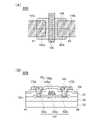
図1(A)は、半導体装置の構成の一形態であるトランジスタ100の構造を説明する上
面図であり、図1(B)は、図1(A)にA1-A2の鎖線で示した部位の積層構造を説
明する断面図である。なお、図1(A)において、基板及び絶縁層の記載は省略している
。FIG. 1A is a top view illustrating the structure of a
図1に示すトランジスタ100は、基板101上に下地層102が形成され、下地層10
2上に酸化物半導体層103が形成されている。また、酸化物半導体層103上にゲート
絶縁層104が形成され、ゲート絶縁層104上にゲート電極105が形成されている。
また、ゲート電極105上に絶縁層107と絶縁層108が形成され、絶縁層108上に
、ソース電極110a及びドレイン電極110bが形成されている。ソース電極110a
及びドレイン電極110bは、ゲート絶縁層104、絶縁層107及び絶縁層108に設
けられたコンタクトホール109を介して、酸化物半導体層103に電気的に接続されて
いる。In the
The
Further, the insulating
The
酸化物半導体層103は、ゲート絶縁層104を介してゲート電極105と重畳するチャ
ネル形成領域103cと、ソース電極110aと電気的に接続するソース領域103aと
、ドレイン電極110bと電気的に接続するドレイン領域103bを有している。The
また、ゲート電極105は、ゲート絶縁層104に接するゲート電極105aと、ゲート
電極105aに積層されたゲート電極105bを有している。Further, the
なお、図1(A)では、コンタクトホール109を、ソース領域103a及びドレイン領
域103b上にそれぞれ複数設ける例を示しているが、ソース領域103a及びドレイン
領域103b上にそれぞれ1つ設ける構成としてもよい。また、ソース電極110aとソ
ース領域103aの接触抵抗、及びドレイン電極110bとドレイン領域103bの接触
抵抗を低減するため、コンタクトホール109は極力大きく、また、コンタクトホール1
09の数を多くすることが好ましい。Although a plurality of contact holes 109 are provided on the
It is preferable to increase the number of 09.
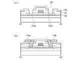
図2に示すトランジスタ140は、トランジスタ100の構成に加えて、ゲート電極10
5の側面にサイドウォール111を有し、酸化物半導体層103のサイドウォール111
と重畳する領域に、低濃度領域103d及び低濃度領域103eを有している。低濃度領
域103dはチャネル形成領域103cとソース領域103aの間に形成され、低濃度領
域103eはチャネル形成領域103cとドレイン領域103bの間に形成されている。
図2(A)は、トランジスタ140の構成を説明する上面図であり、図2(B)は、図2
(A)にB1-B2の鎖線で示した部位の積層構造を説明する断面図である。The
The
The low-
FIG. 2A is a top view illustrating the configuration of the
It is sectional drawing explaining the laminated structure of the part shown by the chain line of B1-B2 in (A).
低濃度領域103d及び低濃度領域103eを設けることにより、トランジスタ特性の劣
化や、短チャネル効果によるしきい値電圧のマイナスシフトを軽減することができる。By providing the
トランジスタ100及びトランジスタ140は、トップゲート構造のトランジスタの一形
態である。The
次に、図1に示すトランジスタ100の作製方法について、図3及び図4を用いて説明す
る。なお、図3及び図4は、図1(A)のA1-A2の鎖線で示した部位の断面に相当す
る。Next, a method for manufacturing the
まず、基板101上に下地層102を50nm以上300nm以下、好ましくは100n
m以上200nm以下の厚さで形成する。基板101は、ガラス基板、セラミック基板の
他、本作製工程の処理温度に耐えうる程度の耐熱性を有するプラスチック基板等を用いる
ことができる。また、基板に透光性を要しない場合には、ステンレス合金等の金属の基板
の表面に絶縁層を設けたものを用いてもよい。ガラス基板としては、例えば、バリウムホ
ウケイ酸ガラス、アルミノホウケイ酸ガラス若しくはアルミノケイ酸ガラス等の無アルカ
リガラス基板を用いるとよい。他に、石英基板、サファイア基板などを用いることができ
る。また、シリコンや炭化シリコンなどの単結晶半導体基板、多結晶半導体基板、シリコ
ンゲルマニウムなどの化合物半導体基板、SOI基板などを適用することも可能であり、
これらの基板上に半導体素子が設けられたものを、基板101として用いてもよい。First, the
It is formed with a thickness of m or more and 200 nm or less. As the
A semiconductor element provided on these substrates may be used as the
下地層102は、窒化アルミニウム、酸化アルミニウム、窒化酸化アルミニウム、酸化窒
化アルミニウム、窒化シリコン、酸化シリコン、窒化酸化シリコンまたは酸化窒化シリコ
ンから選ばれた材料を、単層でまたは積層して形成することができ、基板101からの不
純物元素の拡散を防止する機能を有する。なお、本明細書中において、窒化酸化物とは、
その組成として、酸素よりも窒素の含有量が多いものであって、酸化窒化物とは、その組
成として、窒素よりも酸素の含有量が多いものを示す。なお、各元素の含有量は、例えば
、ラザフォード後方散乱法(RBS:Rutherford Backscatteri
ng Spectrometry)等を用いて測定することができる。The
As its composition, it has a higher nitrogen content than oxygen, and the oxidative nitride has a higher oxygen content than nitrogen as its composition. The content of each element is, for example, Rutherford Backscatteri (RBS).
It can be measured using ng Spectrometry) or the like.
下地層102は、スパッタリング法、CVD法、塗布法、印刷法等を適宜用いることがで
きる。本実施の形態では、下地層102として、窒化シリコンと酸化シリコンの積層を用
いる。具体的には、基板101上に窒化シリコンを50nmの厚さで形成し、該窒化シリ
コン上に酸化シリコンを150nmの厚さで形成する。なお、下地層102中にリン(P
)や硼素(B)がドープされていても良い。For the
) And boron (B) may be doped.
また、下地層102に、塩素、フッ素などのハロゲン元素を含ませることで、基板101
からの不純物元素の拡散を防止する機能をさらに高めることができる。下地層102に含
ませるハロゲン元素の濃度は、SIMS(二次イオン質量分析計)を用いた分析により得
られる濃度ピークにおいて、1×10¹⁵/cm3以上1×1020/cm3以下とすれ
ばよい。Further, by impregnating the
It is possible to further enhance the function of preventing the diffusion of impurity elements from. The concentration of the halogen element contained in the
また、下地層102は、加熱により酸素放出される材料を用いてもよい。「加熱により酸
素放出される」とは、TDS(Thermal Desorption Spectro
scopy:昇温脱離ガス分光法)分析にて、酸素原子に換算しての酸素の放出量が1.
0×1018atoms/cm3以上、好ましくは3.0×1020atoms/cm3
以上であることをいう。Further, the
(Scopy: Heated desorption gas spectroscopy) In the analysis, the amount of oxygen released in terms of oxygen atoms is 1.
0 × 1018 atoms / cm3 or more, preferably 3.0 × 10²⁰ atoms / cm3
That is all.
ここで、TDS分析にて、酸素原子に換算しての酸素の放出量の測定方法について、以下
に説明する。Here, a method for measuring the amount of oxygen released in terms of oxygen atoms by TDS analysis will be described below.
TDS分析したときの気体の放出量は、スペクトルの積分値に比例する。このため、絶縁
層のスペクトルの積分値と、標準試料の基準値に対する比とにより、気体の放出量を計算
することができる。標準試料の基準値とは、所定の原子を含む試料の、スペクトルの積分
値に対する原子の密度の割合である。The amount of gas released during TDS analysis is proportional to the integral value of the spectrum. Therefore, the amount of gas released can be calculated from the integral value of the spectrum of the insulating layer and the ratio to the reference value of the standard sample. The reference value of a standard sample is the ratio of the density of atoms to the integrated value of the spectrum of a sample containing a predetermined atom.
例えば、標準試料である所定の密度の水素を含むシリコンウェハのTDS分析結果、及び
絶縁層のTDS分析結果から、絶縁層の酸素分子の放出量(NO2)は、数式1で求める
ことができる。ここで、TDS分析で得られる質量数32で検出されるスペクトルの全て
が酸素分子由来と仮定する。質量数32のものとしてCH3OHがあるが、存在する可能
性が低いものとしてここでは考慮しない。また、酸素原子の同位体である質量数17の酸
素原子及び質量数18の酸素原子を含む酸素分子についても、自然界における存在比率が
極微量であるため考慮しない。For example, the amount of oxygen molecules released from the insulating layer (NO2 ) can be calculated by
NO2=NH2/SH2×SO2×α (数式1)NO2 = NH2 /SH2 xSO2 x α (Formula 1)
NH2は、標準試料から脱離した水素分子を密度で換算した値である。SH2は、標準試
料をTDS分析したときのスペクトルの積分値である。ここで、標準試料の基準値を、N
H2/SH2とする。SO2は、絶縁層をTDS分析したときのスペクトルの積分値であ
る。αは、TDS分析におけるスペクトル強度に影響する係数である。数式1の詳細に関
しては、特開平6-275697公報を参照する。なお、上記絶縁層の酸素の放出量は、
電子科学株式会社製の昇温脱離分析装置EMD-WA1000S/Wを用い、標準試料と
して1×10¹⁶atoms/cm3の水素原子を含むシリコンウェハを用いて測定した
。NH2 is a value obtained by converting hydrogen molecules desorbed from the standard sample by density.SH2 is an integral value of the spectrum when the standard sample is TDS-analyzed. Here, the reference value of the standard sample is set to N.
H2 / SH2 .SO2 is an integral value of the spectrum when the insulating layer is TDS-analyzed. α is a coefficient that affects the spectral intensity in TDS analysis. For details of
The measurement was carried out using a heated desorption analyzer EMD-WA1000S / W manufactured by Denshi Kagaku Co., Ltd. and a silicon wafer containing 1 × 10¹⁶ atoms / cm3 hydrogen atoms as a standard sample.
また、TDS分析において、酸素の一部は酸素原子として検出される。酸素分子と酸素原
子の比率は、酸素分子のイオン化率から算出することができる。なお、上述のαは酸素分
子のイオン化率を含むため、酸素分子の放出量を評価することで、酸素原子の放出量につ
いても見積もることができる。Also, in TDS analysis, some of the oxygen is detected as oxygen atoms. The ratio of oxygen molecule to oxygen atom can be calculated from the ionization rate of oxygen molecule. Since the above-mentioned α contains the ionization rate of oxygen molecules, the amount of oxygen atoms released can also be estimated by evaluating the amount of oxygen molecules released.
なお、NO2は酸素分子の放出量である。絶縁層においては、酸素原子に換算したときの
酸素の放出量は、酸素分子の放出量の2倍となる。NO2 is the amount of oxygen molecules released. In the insulating layer, the amount of oxygen released when converted to oxygen atoms is twice the amount of oxygen molecules released.
上記構成において、加熱により酸素放出される絶縁層は、酸素が過剰な酸化シリコン(S
iOX(X>2))であってもよい。酸素が過剰な酸化シリコン(SiOX(X>2))
とは、シリコン原子数の2倍より多い酸素原子を単位体積当たりに含むものである。単位
体積当たりのシリコン原子数及び酸素原子数は、ラザフォード後方散乱法により測定した
値である。In the above configuration, the insulating layer in which oxygen is released by heating is silicon oxide (S) in which oxygen is excessive.
It may be iOX (X > 2)). Silicon oxide with excess oxygen (SiOX (X> 2))
Is to contain oxygen atoms per unit volume, which is more than twice the number of silicon atoms. The number of silicon atoms and the number of oxygen atoms per unit volume are values measured by the Rutherford backscattering method.
下地層から酸化物半導体に酸素が供給されることで、下地層及び酸化物半導体の界面準位
を低減できる。この結果、トランジスタの動作などに起因して生じうる電荷などが、上述
の下地層及び酸化物半導体の界面に捕獲されることを抑制することができ、電気特性の劣
化の少ないトランジスタを得ることができる。By supplying oxygen from the base layer to the oxide semiconductor, the interface state of the base layer and the oxide semiconductor can be reduced. As a result, it is possible to prevent the electric charges and the like generated due to the operation of the transistor from being captured at the interface between the above-mentioned base layer and the oxide semiconductor, and it is possible to obtain a transistor with less deterioration in electrical characteristics. can.
さらに、酸化物半導体の酸素欠損に起因して電荷が生じる場合がある。一般に酸化物半導
体の酸素欠損は、一部がドナーとなりキャリアである電子を生じる。この結果、トランジ
スタのしきい値電圧がマイナス方向にシフトしてしまう。この傾向はバックチャネル側で
生じる酸素欠損において顕著である。なお、本明細書におけるバックチャネルとは、酸化
物半導体において下地層の界面近傍を指す。下地層から酸化物半導体に酸素が十分に放出
されることにより、しきい値電圧がマイナス方向へシフトする要因である酸化物半導体の
酸素欠損を補うことができる。Further, charges may be generated due to oxygen deficiency of the oxide semiconductor. In general, oxygen deficiency in oxide semiconductors produces electrons, which are partially donors and carriers. As a result, the threshold voltage of the transistor shifts in the negative direction. This tendency is remarkable in the oxygen deficiency that occurs on the back channel side. The back channel in the present specification refers to the vicinity of the interface of the base layer in the oxide semiconductor. By sufficiently releasing oxygen from the base layer to the oxide semiconductor, it is possible to compensate for the oxygen deficiency of the oxide semiconductor, which is a factor that causes the threshold voltage to shift in the negative direction.
即ち、酸化物半導体に酸素欠損が生じると、下地層と酸化物半導体との界面における電荷
の捕獲を抑制することが困難となるところ、下地層に、加熱により酸素放出される絶縁層
を設けることで、酸化物半導体及び下地層の界面準位、ならびに酸化物半導体の酸素欠損
を低減し、酸化物半導体及び下地層の界面における電荷捕獲の影響を小さくすることがで
きる。That is, when oxygen deficiency occurs in the oxide semiconductor, it becomes difficult to suppress the capture of charge at the interface between the underlayer and the oxide semiconductor. Therefore, an insulating layer that releases oxygen by heating is provided in the underlayer. Therefore, the interface state of the oxide semiconductor and the underlayer, and the oxygen deficiency of the oxide semiconductor can be reduced, and the influence of charge capture at the interface between the oxide semiconductor and the underlayer can be reduced.
また、下地層102には、この後形成する酸化物半導体と同種の成分を含む絶縁材料を用
いてもよい。下地層102を異なる層の積層とする場合には、酸化物半導体に接する層を
酸化物半導体と同種の成分を含む絶縁材料とすればよい。このような材料は酸化物半導体
との相性が良く、これを下地層102に用いることで、酸化物半導体との界面の状態を良
好に保つことができるからである。ここで、「酸化物半導体と同種の成分」とは、酸化物
半導体の構成元素から選択される一または複数の元素を意味する。例えば、酸化物半導体
がIn-Ga-Zn系の酸化物半導体材料によって構成される場合、同種の成分を含む絶
縁材料としては酸化ガリウムなどがある。Further, for the
次に、下地層102上に酸化物半導体を形成する。なお、前処理として、酸化物半導体に
水素、水酸基及び水分がなるべく含まれないようにするために、成膜装置の予備加熱室で
基板101を予備加熱し、基板101や下地層102に吸着した水素、水分などの不純物
を脱離し排気することが好ましい。なお、予備加熱室に設ける排気手段はクライオポンプ
が好ましい。なお、この予備加熱の処理は省略することもできる。またこの予備加熱は、
下地層102の成膜前に、基板101にも同様に行ってもよい。Next, an oxide semiconductor is formed on the
The same may be performed on the
酸化物半導体としては、少なくともインジウム(In)あるいは亜鉛(Zn)を含むこと
が好ましい。特にInとZnを含むことが好ましい。また、該酸化物半導体を用いたトラ
ンジスタの電気特性のばらつきを減らすためのスタビライザーとして、それらに加えてガ
リウム(Ga)を有することが好ましい。また、スタビライザーとしてスズ(Sn)を有
することが好ましい。また、スタビライザーとしてハフニウム(Hf)を有することが好
ましい。また、スタビライザーとしてアルミニウム(Al)を有することが好ましい。The oxide semiconductor preferably contains at least indium (In) or zinc (Zn). In particular, it is preferable to contain In and Zn. Further, it is preferable to have gallium (Ga) in addition to the stabilizer for reducing the variation in the electrical characteristics of the transistor using the oxide semiconductor. Further, it is preferable to have tin (Sn) as the stabilizer. Further, it is preferable to have hafnium (Hf) as a stabilizer. Further, it is preferable to have aluminum (Al) as the stabilizer.
また、他のスタビライザーとして、ランタノイドである、ランタン(La)、セリウム(
Ce)、プラセオジム(Pr)、ネオジム(Nd)、サマリウム(Sm)、ユウロピウム
(Eu)、ガドリニウム(Gd)、テルビウム(Tb)、ジスプロシウム(Dy)、ホル
ミウム(Ho)、エルビウム(Er)、ツリウム(Tm)、イッテルビウム(Yb)、ル
テチウム(Lu)のいずれか一種あるいは複数種を有してもよい。In addition, as other stabilizers, lanthanoids such as lanthanum (La) and cerium (
Ce), placeodim (Pr), neodym (Nd), samarium (Sm), europium (Eu), gadolinium (Gd), terbium (Tb), dysprosium (Dy), lutetium (Ho), erbium (Er), thulium ( It may have one or more of Tm), itterbium (Yb), and lutetium (Lu).
例えば、酸化物半導体として、酸化インジウム、酸化スズ、酸化亜鉛、二元系金属の酸化
物であるIn-Zn系酸化物、Sn-Zn系酸化物、Al-Zn系酸化物、Zn-Mg系
酸化物、Sn-Mg系酸化物、In-Mg系酸化物、In-Ga系酸化物、三元系金属の
酸化物であるIn-Ga-Zn系酸化物(IGZOとも表記する)、In-Al-Zn系
酸化物、In-Sn-Zn系酸化物、Sn-Ga-Zn系酸化物、Al-Ga-Zn系酸
化物、Sn-Al-Zn系酸化物、In-Hf-Zn系酸化物、In-La-Zn系酸化
物、In-Ce-Zn系酸化物、In-Pr-Zn系酸化物、In-Nd-Zn系酸化物
、In-Sm-Zn系酸化物、In-Eu-Zn系酸化物、In-Gd-Zn系酸化物、
In-Tb-Zn系酸化物、In-Dy-Zn系酸化物、In-Ho-Zn系酸化物、I
n-Er-Zn系酸化物、In-Tm-Zn系酸化物、In-Yb-Zn系酸化物、In
-Lu-Zn系酸化物、四元系金属の酸化物であるIn-Sn-Ga-Zn系酸化物、I
n-Hf-Ga-Zn系酸化物、In-Al-Ga-Zn系酸化物、In-Sn-Al-
Zn系酸化物、In-Sn-Hf-Zn系酸化物、In-Hf-Al-Zn系酸化物を用
いることができる。For example, as oxide semiconductors, indium oxide, tin oxide, zinc oxide, In—Zn-based oxides, Sn—Zn-based oxides, Al—Zn-based oxides, Zn—Mg-based oxides of binary metals, etc. Oxides, Sn-Mg-based oxides, In-Mg-based oxides, In-Ga-based oxides, In-Ga-Zn-based oxides (also referred to as IGZO), which are ternary metal oxides, In- Al-Zn-based oxide, In-Sn-Zn-based oxide, Sn-Ga-Zn-based oxide, Al-Ga-Zn-based oxide, Sn-Al-Zn-based oxide, In-Hf-Zn-based oxidation Material, In-La-Zn-based oxide, In-Ce-Zn-based oxide, In-Pr-Zn-based oxide, In-Nd-Zn-based oxide, In-Sm-Zn-based oxide, In-Eu -Zn-based oxide, In-Gd-Zn-based oxide,
In-Tb-Zn-based oxide, In-Dy-Zn-based oxide, In-Ho-Zn-based oxide, I
n-Er-Zn-based oxide, In-Tm-Zn-based oxide, In-Yb-Zn-based oxide, In
-Lu-Zn-based oxide, In-Sn-Ga-Zn-based oxide, which is a quaternary metal oxide, I
n-Hf-Ga-Zn-based oxide, In-Al-Ga-Zn-based oxide, In-Sn-Al-
Zn-based oxides, In—Sn—Hf—Zn-based oxides, and In—Hf-Al—Zn-based oxides can be used.
酸化物半導体層は、好ましくはInを含有する酸化物半導体、さらに好ましくは、In、
及びGaを含有する酸化物半導体である。The oxide semiconductor layer is preferably an oxide semiconductor containing In, more preferably In,
It is an oxide semiconductor containing Ga and Ga.
ここで、例えば、In-Ga-Zn系酸化物とは、インジウム(In)、ガリウム(Ga
)、亜鉛(Zn)を有する酸化物という意味であり、InとGaとZnの比率は問わない
。また、InとGaとZn以外の金属元素を含んでもよい。Here, for example, the In—Ga—Zn-based oxides are indium (In) and gallium (Ga).
), It means an oxide having zinc (Zn), and the ratio of In, Ga, and Zn does not matter. Further, it may contain a metal element other than In, Ga and Zn.
また、酸化物半導体層は、化学式InMO3(ZnO)m(m>0)で表記される薄膜を
用いることができる。ここで、Mは、Sn、Zn、Ga、Al、MnおよびCoから選ば
れた一または複数の金属元素を示す。また、酸化物半導体として、In3SnO5(Zn
O)n(n>0)で表記される材料を用いてもよい。Further, as the oxide semiconductor layer, a thin film represented by the chemical formula InMO3 (ZnO)m (m> 0) can be used. Here, M represents one or more metal elements selected from Sn, Zn, Ga, Al, Mn and Co. Further, as an oxide semiconductor, In3 SnO5 (Zn).
O) The material represented byn (n> 0) may be used.
例えば、In:Ga:Zn=1:1:1(=1/3:1/3:1/3)あるいはIn:G
a:Zn=2:2:1(=2/5:2/5:1/5)の原子数比のIn-Ga-Zn系酸
化物やその組成の近傍の酸化物を用いることができる。あるいは、In:Sn:Zn=1
:1:1(=1/3:1/3:1/3)、In:Sn:Zn=2:1:3(=1/3:1
/6:1/2)あるいはIn:Sn:Zn=2:1:5(=1/4:1/8:5/8)の
原子数比のIn-Sn-Zn系酸化物やその組成の近傍の酸化物を用いるとよい。For example, In: Ga: Zn = 1: 1: 1 (= 1/3: 1/3: 1/3) or In: G
In—Ga—Zn-based oxides having an atomic number ratio of a: Zn = 2: 2: 1 (= 2/5: 2/5: 1/5) or oxides in the vicinity of the composition can be used. Alternatively, In: Sn: Zn = 1
1: 1 (= 1/3: 1/3: 1/3), In: Sn: Zn = 2: 1: 3 (= 1/3: 1)
/ 6: 1/2) or In: Sn: Zn = 2: 1: 5 (= 1/4: 1/8: 5/8) In—Sn—Zn-based oxide having an atomic number ratio or its composition It is advisable to use a nearby oxide.
しかし、これらに限られず、必要とする半導体特性(移動度、しきい値、ばらつき等)に
応じて適切な組成のものを用いればよい。また、必要とする半導体特性を得るために、キ
ャリア密度や不純物濃度、欠陥密度、金属元素と酸素の原子数比、原子間結合距離、密度
等を適切なものとすることが好ましい。However, the present invention is not limited to these, and a semiconductor having an appropriate composition may be used according to the required semiconductor characteristics (mobility, threshold value, variation, etc.). Further, in order to obtain the required semiconductor characteristics, it is preferable that the carrier density, the impurity concentration, the defect density, the atomic number ratio between the metal element and oxygen, the interatomic bond distance, the density and the like are appropriate.
例えば、In-Sn-Zn系酸化物では比較的容易に高い移動度が得られる。しかしなが
ら、In-Ga-Zn系酸化物でも、バルク内欠陥密度を低減することにより移動度を上
げることができる。For example, high mobility can be obtained relatively easily with an In—Sn—Zn-based oxide. However, even with In—Ga—Zn-based oxides, the mobility can be increased by reducing the defect density in the bulk.
なお、例えば、In、Ga、Znの原子数比がIn:Ga:Zn=a:b:c(a+b+
c=1)である酸化物の組成が、原子数比がIn:Ga:Zn=A:B:C(A+B+C
=1)の酸化物の組成の近傍であるとは、a、b、cが、
(a―A)2+(b―B)2+(c―C)2≦r2
を満たすことをいい、rは、例えば、0.05とすればよい。他の酸化物でも同様である
。For example, the atomic number ratio of In, Ga, and Zn is In: Ga: Zn = a: b: c (a + b +).
The composition of the oxide having c = 1) has an atomic number ratio of In: Ga: Zn = A: B: C (A + B + C).
= 1) When a, b, and c are in the vicinity of the oxide composition,
(A-A)2 + (b-B)2 + (c-C)2 ≤ r2
It means that the condition is satisfied, and r may be, for example, 0.05. The same applies to other oxides.
酸化物半導体は単結晶でも、非単結晶でもよい。後者の場合、アモルファスでも、多結晶
でもよい。また、アモルファス中に結晶性を有する部分を含む構造でも、非アモルファス
でもよい。The oxide semiconductor may be a single crystal or a non-single crystal. In the latter case, it may be amorphous or polycrystalline. Further, the structure may be an amorphous structure including a crystalline portion, or may be non-amorphous.
アモルファス状態の酸化物半導体は、比較的容易に平坦な表面を得ることができるため、
これを用いてトランジスタを作製した際の界面散乱を低減でき、比較的容易に、比較的高
い移動度を得ることができる。Since the amorphous oxide semiconductor can obtain a flat surface relatively easily, it is possible to obtain a flat surface.
Using this, interfacial scattering can be reduced when a transistor is manufactured, and relatively high mobility can be obtained relatively easily.
また、結晶性を有する酸化物半導体では、よりバルク内欠陥を低減することができ、表面
の平坦性を高めればアモルファス状態の酸化物半導体以上の移動度を得ることができる。
表面の平坦性を高めるためには、平坦な表面上に酸化物半導体を形成することが好ましく
、具体的には、平均面粗さ(Ra)が1nm以下、好ましくは0.3nm以下、より好ま
しくは0.1nm以下の表面上に形成するとよい。なお、Raは原子間力顕微鏡(AFM
:Atomic Force Microscope)にて評価可能である。Further, in the oxide semiconductor having crystallinity, defects in the bulk can be further reduced, and if the surface flatness is improved, the mobility higher than that of the oxide semiconductor in the amorphous state can be obtained.
In order to improve the flatness of the surface, it is preferable to form an oxide semiconductor on a flat surface, and specifically, the average surface roughness (Ra) is 1 nm or less, preferably 0.3 nm or less, more preferably. May be formed on a surface of 0.1 nm or less. Ra is an atomic force microscope (AFM).
: Atomic Force Microscope) can be evaluated.
結晶性を有する酸化物半導体としては、CAAC-OS(C Axis Aligned
Crystalline Oxide Semiconductor)が好ましい。C
AAC-OSは、完全な単結晶ではなく、完全な非晶質でもない。CAAC-OSは、非
晶質相に結晶部を有する結晶-非晶質混相構造の酸化物半導体である。なお、当該結晶部
は、一辺が100nm未満の立方体内に収まる大きさであることが多い。また、透過型電
子顕微鏡(TEM:Transmission Electron Microscop
e)による観察像では、CAAC-OSに含まれる非晶質部と結晶部との境界は明確では
ない。また、TEMによってCAAC-OSには粒界(グレインバウンダリーともいう。
)は確認できない。そのため、CAAC-OSは、粒界に起因する電子移動度の低下が抑
制される。As a crystalline oxide semiconductor, CAAC-OS (C Axis Aligned)
Crystalline Oxide Semiconductor) is preferable. C
AAC-OS is neither completely single crystal nor completely amorphous. CAAC-OS is an oxide semiconductor having a crystal-amorphous mixed phase structure having a crystal portion in an amorphous phase. In many cases, the crystal portion has a size that can be accommodated in a cube having a side of less than 100 nm. In addition, a transmission electron microscope (TEM: Transmission Electron Microscope)
In the observation image according to e), the boundary between the amorphous part and the crystalline part contained in CAAC-OS is not clear. Also, by TEM, the CAAC-OS has grain boundaries (also called grain boundaries).
) Cannot be confirmed. Therefore, the CAAC-OS suppresses the decrease in electron mobility due to the grain boundaries.
CAAC-OSに含まれる結晶部は、c軸がCAAC-OSの被形成面の法線ベクトルま
たは表面の法線ベクトルに平行な方向に揃い、かつab面に垂直な方向から見て三角形状
または六角形状の原子配列を有し、c軸に垂直な方向から見て金属原子が層状または金属
原子と酸素原子とが層状に配列している。なお、異なる結晶部間で、それぞれa軸および
b軸の向きが異なっていてもよい。本明細書において、単に垂直と記載する場合、85°
以上95°以下の範囲も含まれることとする。また、単に平行と記載する場合、-5°以
上5°以下の範囲も含まれることとする。The crystal part contained in CAAC-OS is aligned in a direction in which the c-axis is parallel to the normal vector of the surface to be formed or the normal vector of the surface of CAAC-OS, and is triangular or triangular when viewed from the direction perpendicular to the ab plane. It has a hexagonal atomic arrangement, and metal atoms are arranged in layers or metal atoms and oxygen atoms are arranged in layers when viewed from the direction perpendicular to the c-axis. The directions of the a-axis and the b-axis may be different between different crystal portions. In the present specification, when it is simply described as vertical, it is 85 °.
The range of 95 ° or more is also included. In addition, when it is simply described as parallel, the range of -5 ° or more and 5 ° or less is also included.
なお、CAAC-OSにおいて、結晶部の分布が一様でなくてもよい。例えば、CAAC
-OSの形成過程において、酸化物半導体膜の表面側から結晶成長させる場合、被形成面
の近傍に対し表面の近傍では結晶部の占める割合が高くなることがある。また、CAAC
-OSへ不純物を添加することにより、当該不純物添加領域において結晶部が非晶質化す
ることもある。In CAAC-OS, the distribution of crystal portions does not have to be uniform. For example, CAAC
-In the process of forming the OS, when the crystal is grown from the surface side of the oxide semiconductor film, the ratio of the crystal portion may be higher in the vicinity of the surface than in the vicinity of the surface to be formed. Also, CAAC
-By adding an impurity to the OS, the crystal part may become amorphous in the impurity-added region.
CAAC-OSに含まれる結晶部のc軸は、CAAC-OSの被形成面の法線ベクトルま
たは表面の法線ベクトルに平行な方向に揃うため、CAAC-OSの形状(被形成面の断
面形状または表面の断面形状)によっては互いに異なる方向を向くことがある。なお、結
晶部のc軸の方向は、CAAC-OSが形成されたときの被形成面の法線ベクトルまたは
表面の法線ベクトルに平行な方向となる。結晶部は、成膜することにより、または成膜後
に加熱処理などの結晶化処理を行うことにより形成される。Since the c-axis of the crystal portion included in CAAC-OS is aligned in the direction parallel to the normal vector of the surface to be formed or the normal vector of the surface of CAAC-OS, the shape of CAAC-OS (cross-sectional shape of the surface to be formed). Or, depending on the cross-sectional shape of the surface), they may face different directions. The direction of the c-axis of the crystal portion is parallel to the normal vector of the surface to be formed or the normal vector of the surface when CAAC-OS is formed. The crystallized portion is formed by forming a film or by performing a crystallization treatment such as a heat treatment after the film formation.
CAAC-OSは、その組成などに応じて、導体であったり、半導体であったり、絶縁体
であったりする。また、その組成などに応じて、可視光に対して透明であったり不透明で
あったりする。なお、CAAC-OSの一部は窒素で置換されてもよい。The CAAC-OS may be a conductor, a semiconductor, or an insulator, depending on its composition and the like. Further, it may be transparent or opaque to visible light depending on its composition and the like. A part of CAAC-OS may be replaced with nitrogen.
CAAC-OSを用いたトランジスタは、可視光や紫外光の照射による電気特性の変動を
低減することが可能である。よって、当該トランジスタは、信頼性が高い。A transistor using CAAC-OS can reduce fluctuations in electrical characteristics due to irradiation with visible light or ultraviolet light. Therefore, the transistor is highly reliable.
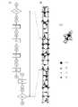
CAAC-OSに含まれる結晶構造の一例について図15乃至図17を用いて詳細に説明
する。なお、特に断りがない限り、図15乃至図17は上方向をc軸方向とし、c軸方向
と直交する面をab面とする。なお、単に上半分、下半分という場合、ab面を境にした
場合の上半分、下半分をいう。また、図15において、丸で囲まれたOは4配位のOを示
し、二重丸で囲まれたOは3配位のOを示す。An example of the crystal structure contained in CAAC-OS will be described in detail with reference to FIGS. 15 to 17. Unless otherwise specified, in FIGS. 15 to 17, the upward direction is the c-axis direction, and the plane orthogonal to the c-axis direction is the ab plane. The upper half and the lower half refer to the upper half and the lower half when the ab surface is used as a boundary. Further, in FIG. 15, the circled O indicates a 4-coordinated O, and the double-circulated O indicates a 3-coordinated O.
図15(A)に、1個の6配位のInと、Inに近接の6個の4配位の酸素原子(以下4
配位のO)と、を有する構造を示す。ここでは、金属原子が1個に対して、近接の酸素原
子のみ示した構造を小グループと呼ぶ。図15(A)の構造は、八面体構造をとるが、簡
単のため平面構造で示している。なお、図15(A)の上半分および下半分にはそれぞれ
3個ずつ4配位のOがある。図15(A)に示す小グループは電荷が0である。In FIG. 15A, one 6-coordinated In and 6 4-coordinated oxygen atoms close to In (hereinafter 4).
The structure having O) of coordination is shown. Here, a structure showing only oxygen atoms in the vicinity of one metal atom is called a small group. The structure of FIG. 15A has an octahedral structure, but is shown as a planar structure for simplicity. In addition, there are three O's in each of the upper half and the lower half of FIG. 15A. The small group shown in FIG. 15A has zero charge.
図15(B)に、1個の5配位のGaと、Gaに近接の3個の3配位の酸素原子(以下3
配位のO)と、Gaに近接の2個の4配位のOと、を有する構造を示す。3配位のOは、
いずれもab面に存在する。図15(B)の上半分および下半分にはそれぞれ1個ずつ4
配位のOがある。また、Inも5配位をとるため、図15(B)に示す構造をとりうる。
図15(B)に示す小グループは電荷が0である。In FIG. 15B, one 5-coordinated Ga and three 3-coordinated oxygen atoms close to Ga (hereinafter, 3).
Shown shows a structure having an O) of coordination and two 4-coordinated Os in close proximity to Ga. O of 3 coordination is
Both exist on the ab surface. 1 in each of the upper and lower halves of FIG. 15 (B) 4
There is a coordination O. Further, since In also has five coordinations, the structure shown in FIG. 15B can be adopted.
The small group shown in FIG. 15B has zero charge.
図15(C)に、1個の4配位のZnと、Znに近接の4個の4配位のOと、を有する構
造を示す。図15(C)の上半分には1個の4配位のOがあり、下半分には3個の4配位
のOがある。または、図15(C)の上半分に3個の4配位のOがあり、下半分に1個の
4配位のOがあってもよい。図15(C)に示す小グループは電荷が0である。FIG. 15C shows a structure having one 4-coordinated Zn and four 4-coordinated O close to Zn. The upper half of FIG. 15C has one 4-coordinated O, and the lower half has three 4-coordinated O's. Alternatively, there may be three 4-coordinated O's in the upper half of FIG. 15C and one 4-coordinated O in the lower half. The small group shown in FIG. 15C has zero charge.
図15(D)に、1個の6配位のSnと、Snに近接の6個の4配位のOと、を有する構
造を示す。図15(D)の上半分には3個の4配位のOがあり、下半分には3個の4配位
のOがある。図15(D)に示す小グループは電荷が+1となる。FIG. 15D shows a structure having one 6-coordinated Sn and 6 4-coordinated O's in close proximity to Sn. The upper half of FIG. 15 (D) has three 4-coordinated O's, and the lower half has three 4-coordinated O's. The small group shown in FIG. 15 (D) has a charge of +1.
図15(E)に、2個のZnを含む小グループを示す。図15(E)の上半分には1個の
4配位のOがあり、下半分には1個の4配位のOがある。図15(E)に示す小グループ
は電荷が-1となる。FIG. 15E shows a small group containing two Zns. The upper half of FIG. 15 (E) has one 4-coordinated O, and the lower half has one 4-coordinated O. The small group shown in FIG. 15 (E) has a charge of -1.
ここでは、複数の小グループの集合体を中グループと呼び、複数の中グループの集合体を
大グループ(ユニットセルともいう。)と呼ぶ。Here, an aggregate of a plurality of small groups is referred to as a medium group, and an aggregate of a plurality of medium groups is referred to as a large group (also referred to as a unit cell).
ここで、これらの小グループ同士が結合する規則について説明する。図15(A)に示す
6配位のInの上半分の3個のOは、下方向にそれぞれ3個の近接Inを有し、下半分の
3個のOは、上方向にそれぞれ3個の近接Inを有する。図15(B)に示す5配位のG
aの上半分の1個のOは、下方向に1個の近接Gaを有し、下半分の1個のOは、上方向
に1個の近接Gaを有する。図15(C)に示す4配位のZnの上半分の1個のOは、下
方向に1個の近接Znを有し、下半分の3個のOは、上方向にそれぞれ3個の近接Znを
有する。この様に、金属原子の上方向の4配位のOの数と、そのOの下方向にある近接金
属原子の数は等しく、同様に金属原子の下方向の4配位のOの数と、そのOの上方向にあ
る近接金属原子の数は等しい。Oは4配位なので、下方向にある近接金属原子の数と、上
方向にある近接金属原子の数の和は4になる。従って、金属原子の上方向にある4配位の
Oの数と、別の金属原子の下方向にある4配位のOの数との和が4個のとき、金属原子を
有する二種の小グループ同士は結合することができる。例えば、6配位の金属原子(In
またはSn)が下半分の4配位のOを介して結合する場合、4配位のOが3個であるため
、5配位の金属原子(GaまたはIn)または4配位の金属原子(Zn)のいずれかと結
合することになる。Here, the rules for joining these small groups will be described. The three Os in the upper half of the six-coordinated Ins shown in FIG. 15 (A) each have three proximity Ins in the downward direction, and the three Os in the lower half each have three in the upward direction. Has a proximity In. Five-coordinated G shown in FIG. 15 (B)
One O in the upper half of a has one proximity Ga in the downward direction, and one O in the lower half has one proximity Ga in the upward direction. One O in the upper half of the four-coordinated Zn shown in FIG. 15C has one adjacent Zn in the downward direction, and three Os in the lower half each have three O in the upward direction. It has a proximity Zn. Thus, the number of upward four-coordinated O's of a metal atom is equal to the number of adjacent metal atoms below that O, and similarly the number of downward four-coordinated O's of the metal atom. , The number of adjacent metal atoms in the upward direction of O is equal. Since O is 4-coordinated, the sum of the number of nearby metal atoms in the downward direction and the number of nearby metal atoms in the upward direction is 4. Therefore, when the sum of the number of 4-coordinated O's in the upward direction of a metal atom and the number of 4-coordinated O's in the downward direction of another metal atom is 4, two kinds having a metal atom. Small groups can be combined. For example, a 6-coordinated metal atom (In)
Or Sn) is bonded via a 4-coordinated O in the lower half, and since there are 3 4-coordinated O's, a 5-coordinated metal atom (Ga or In) or a 4-coordinated metal atom (or 4) It will be bonded to any of Zn).
これらの配位数を有する金属原子は、c軸方向において、4配位のOを介して結合する。
また、このほかにも、層構造の合計の電荷が0となるように複数の小グループが結合して
中グループを構成する。Metal atoms having these coordination numbers are bonded via a 4-coordination O in the c-axis direction.
In addition to this, a plurality of small groups are combined to form a middle group so that the total charge of the layer structure becomes 0.
図16(A)に、In-Sn-Zn系酸化物の層構造を構成する中グループのモデル図を
示す。図16(B)に、3つの中グループで構成される大グループを示す。なお、図16
(C)は、図16(B)の層構造をc軸方向から観察した場合の原子配列を示す。FIG. 16A shows a model diagram of the middle group constituting the layer structure of the In—Sn—Zn-based oxide. FIG. 16B shows a large group composed of three medium groups. In addition, FIG.
(C) shows the atomic arrangement when the layer structure of FIG. 16 (B) is observed from the c-axis direction.
図16(A)においては、簡単のため、3配位のOは省略し、4配位のOは個数のみ示し
、例えば、Snの上半分および下半分にはそれぞれ3個ずつ4配位のOがあることを丸枠
の3として示している。同様に、図16(A)において、Inの上半分および下半分には
それぞれ1個ずつ4配位のOがあり、丸枠の1として示している。また、同様に、図16
(A)において、下半分には1個の4配位のOがあり、上半分には3個の4配位のOがあ
るZnと、上半分には1個の4配位のOがあり、下半分には3個の4配位のOがあるZn
とを示している。In FIG. 16A, for the sake of simplicity, the O of the 3-coordination is omitted, and only the number of the O of the 4-coordination is shown. The presence of O is shown as 3 in the round frame. Similarly, in FIG. 16A, there is one 4-coordinated O in each of the upper half and the lower half of In, and they are shown as 1 in a round frame. Similarly, FIG. 16
In (A), the lower half has one 4-coordinated O, the upper half has three 4-coordinated O's, and the upper half has one 4-coordinated O. Yes, there are 3 4-coordinated O's in the lower half Zn
It shows that.
図16(A)において、In-Sn-Zn系酸化物の層構造を構成する中グループは、上
から順に4配位のOが3個ずつ上半分および下半分にあるSnが、4配位のOが1個ずつ
上半分および下半分にあるInと結合し、そのInが、上半分に3個の4配位のOがある
Znと結合し、そのZnの下半分の1個の4配位のOを介して4配位のOが3個ずつ上半
分および下半分にあるInと結合し、そのInが、上半分に1個の4配位のOがあるZn
2個からなる小グループと結合し、この小グループの下半分の1個の4配位のOを介して
4配位のOが3個ずつ上半分および下半分にあるSnと結合している構成である。この中
グループが複数結合して大グループを構成する。In FIG. 16A, in the middle group constituting the layer structure of the In—Sn—Zn-based oxide, three 4-coordinated O's are arranged in order from the top, and Sn in the upper half and the lower half is 4-coordinated. O is bonded to In in the upper half and the lower half one by one, and that In is bonded to Zn having three 4-coordinated O in the upper half, and one 4 in the lower half of the Zn. Three 4-coordinated O bonds are combined with In in the upper half and the lower half through the coordinated O, and the In is Zn with one 4-coordinated O in the upper half.
It is combined with a small group of two, and through one 4-coordinated O in the lower half of this small group, three 4-coordinated O's are combined with Sn in the upper and lower halves. It is a composition. Multiple middle groups are combined to form a large group.
ここで、3配位のOおよび4配位のOの場合、結合1本当たりの電荷はそれぞれ-0.6
67、-0.5と考えることができる。例えば、In(6配位または5配位)、Zn(4
配位)、Sn(5配位または6配位)の電荷は、それぞれ+3、+2、+4である。従っ
て、Snを含む小グループは電荷が+1となる。そのため、Snを含む層構造を形成する
ためには、電荷+1を打ち消す電荷-1が必要となる。電荷-1をとる構造として、図1
5(E)に示すように、2個のZnを含む小グループが挙げられる。例えば、Snを含む
小グループが1個に対し、2個のZnを含む小グループが1個あれば、電荷が打ち消され
るため、層構造の合計の電荷を0とすることができる。Here, in the case of 3-coordinated O and 4-coordinated O, the charge per bond is -0.6, respectively.
It can be considered as 67, -0.5. For example, In (6 or 5 coordinates), Zn (4)
The charges of (coordination) and Sn (5-coordination or 6-coordination) are +3, +2, and +4, respectively. Therefore, the small group containing Sn has a charge of +1. Therefore, in order to form a layer structure containing Sn, a charge -1 that cancels the charge +1 is required. FIG. 1 shows a structure that takes an electric charge of -1.
As shown in 5 (E), a small group containing two Zn can be mentioned. For example, if there is one small group containing Sn and one small group containing two Zn, the charges are canceled, so that the total charge of the layer structure can be set to 0.
具体的には、図16(B)に示した大グループが繰り返されることで、In-Sn-Zn
系酸化物の結晶(In2SnZn3O8)を得ることができる。なお、得られるIn-S
n-Zn系酸化物の層構造は、In2SnZn2O7(ZnO)m(mは0または自然数
。)とする組成式で表すことができる。Specifically, by repeating the large group shown in FIG. 16 (B), In—Sn—Zn
Crystals of system oxides (In2 SnZn3 O8 ) can be obtained. The obtained In-S
The layer structure of the n—Zn-based oxide can be expressed by a composition formula of In2 SnZn2 O7 (ZnO)m (m is 0 or a natural number).
また、このほかにも、四元系金属の酸化物であるIn-Sn-Ga-Zn系酸化物や、三
元系金属の酸化物であるIn-Ga-Zn系酸化物(IGZOとも表記する。)、In-
Al-Zn系酸化物、Sn-Ga-Zn系酸化物、Al-Ga-Zn系酸化物、Sn-A
l-Zn系酸化物や、In-Hf-Zn系酸化物、In-La-Zn系酸化物、In-C
e-Zn系酸化物、In-Pr-Zn系酸化物、In-Nd-Zn系酸化物、In-Sm
-Zn系酸化物、In-Eu-Zn系酸化物、In-Gd-Zn系酸化物、In-Tb-
Zn系酸化物、In-Dy-Zn系酸化物、In-Ho-Zn系酸化物、In-Er-Z
n系酸化物、In-Tm-Zn系酸化物、In-Yb-Zn系酸化物、In-Lu-Zn
系酸化物や、二元系金属の酸化物であるIn-Zn系酸化物、Sn-Zn系酸化物、Al
-Zn系酸化物、Zn-Mg系酸化物、Sn-Mg系酸化物、In-Mg系酸化物や、I
n-Ga系酸化物、などを用いた場合も同様である。In addition to this, In-Sn-Ga-Zn-based oxide, which is an oxide of a quaternary metal, and In-Ga-Zn-based oxide, which is an oxide of a ternary metal (also referred to as IGZO). .), In-
Al-Zn-based oxide, Sn-Ga-Zn-based oxide, Al-Ga-Zn-based oxide, Sn-A
l-Zn-based oxide, In-Hf-Zn-based oxide, In-La-Zn-based oxide, In-C
e-Zn-based oxide, In-Pr-Zn-based oxide, In-Nd-Zn-based oxide, In-Sm
-Zn-based oxide, In-Eu-Zn-based oxide, In-Gd-Zn-based oxide, In-Tb-
Zn-based oxide, In-Dy-Zn-based oxide, In-Ho-Zn-based oxide, In-Er-Z
n-based oxide, In-Tm-Zn-based oxide, In-Yb-Zn-based oxide, In-Lu-Zn
In-Zn-based oxides, Sn—Zn-based oxides, and Al, which are system oxides and oxides of binary metals.
-Zn-based oxides, Zn-Mg-based oxides, Sn-Mg-based oxides, In-Mg-based oxides, and I
The same applies when an n—Ga-based oxide or the like is used.
例えば、図17(A)に、In-Ga-Zn系酸化物の層構造を構成する中グループのモ
デル図を示す。For example, FIG. 17A shows a model diagram of the middle group constituting the layer structure of the In—Ga—Zn-based oxide.
図17(A)において、In-Ga-Zn系酸化物の層構造を構成する中グループは、上
から順に4配位のOが3個ずつ上半分および下半分にあるInが、4配位のOが1個上半
分にあるZnと結合し、そのZnの下半分の3個の4配位のOを介して、4配位のOが1
個ずつ上半分および下半分にあるGaと結合し、そのGaの下半分の1個の4配位のOを
介して、4配位のOが3個ずつ上半分および下半分にあるInと結合している構成である
。この中グループが複数結合して大グループを構成する。In FIG. 17 (A), in the middle group constituting the layer structure of the In—Ga—Zn-based oxide, three 4-coordinated O bonds are arranged in order from the top, and three Ins in the upper half and the lower half are 4-coordinated. O is combined with Zn in the upper half of the Zn, and O in the 4-coordination is 1 through the three 4-coordinated O in the lower half of the Zn.
It binds to Ga in the upper and lower halves one by one, and through one four-coordinated O in the lower half of the Ga, three four-coordinated O's with In in the upper and lower halves. It is a combined configuration. Multiple middle groups are combined to form a large group.
図17(B)に3つの中グループで構成される大グループを示す。なお、図17(C)は
、図17(B)の層構造をc軸方向から観察した場合の原子配列を示している。FIG. 17B shows a large group composed of three medium groups. Note that FIG. 17C shows the atomic arrangement when the layer structure of FIG. 17B is observed from the c-axis direction.
ここで、In(6配位または5配位)、Zn(4配位)、Ga(5配位)の電荷は、それ
ぞれ+3、+2、+3であるため、In、ZnおよびGaのいずれかを含む小グループは
、電荷が0となる。そのため、これらの小グループの組み合わせであれば中グループの合
計の電荷は常に0となる。Here, since the charges of In (6-coordinated or 5-coordinated), Zn (4-coordinated), and Ga (5-coordinated) are +3, +2, and +3, respectively, any of In, Zn, and Ga can be used. The small group containing has zero charge. Therefore, in the case of a combination of these small groups, the total charge of the middle group is always 0.
また、In-Ga-Zn系酸化物の層構造を構成する中グループは、図17(A)に示し
た中グループに限定されず、In、Ga、Znの配列が異なる中グループを組み合わせた
大グループも取りうる。Further, the middle group constituting the layer structure of the In—Ga—Zn-based oxide is not limited to the middle group shown in FIG. 17 (A), and is a large combination of middle groups having different arrangements of In, Ga, and Zn. You can also take a group.
具体的には、図17(B)に示した大グループが繰り返されることで、In-Ga-Zn
系酸化物の結晶を得ることができる。なお、得られるIn-Ga-Zn系酸化物の層構造
は、InGaO3(ZnO)n(nは自然数。)とする組成式で表すことができる。Specifically, by repeating the large group shown in FIG. 17 (B), In-Ga-Zn
Crystals of system oxides can be obtained. The layered structure of the obtained In—Ga—Zn-based oxide can be represented by a composition formula of InGaO3 (ZnO)n (n is a natural number).
n=1(InGaZnO4)の場合は、例えば、図18(A)に示す結晶構造を取りうる
。なお、図18(A)に示す結晶構造において、図15(B)で説明したように、Ga及
びInは5配位をとるため、GaがInに置き換わった構造も取りうる。When n = 1 (InGaZnO4 ), for example, the crystal structure shown in FIG. 18 (A) can be taken. In the crystal structure shown in FIG. 18 (A), as described in FIG. 15 (B), Ga and In have five coordinations, so that a structure in which Ga is replaced with In can also be taken.
また、n=2(InGaZn2O5)の場合は、例えば、図18(B)に示す結晶構造を
取りうる。なお、図18(B)に示す結晶構造において、図15(B)で説明したように
、Ga及びInは5配位をとるため、GaがInに置き換わった構造も取りうる。Further, in the case of n = 2 (InGaZn2 O5 ), for example, the crystal structure shown in FIG. 18 (B) can be taken. In the crystal structure shown in FIG. 18 (B), as described in FIG. 15 (B), Ga and In have five coordinations, so that a structure in which Ga is replaced with In can also be taken.
本実施の形態では、まず、下地層102上に、スパッタリング法により1nm以上10n
m以下の第1の酸化物半導体を形成する。第1の酸化物半導体を形成する時の基板温度は
200℃以上400℃以下とする。In the present embodiment, first, on the
A first oxide semiconductor of m or less is formed. The substrate temperature at the time of forming the first oxide semiconductor is 200 ° C. or higher and 400 ° C. or lower.
ここで、酸化物半導体を形成するスパッタリング装置について、以下に詳細を説明する。Here, the details of the sputtering apparatus for forming the oxide semiconductor will be described below.
酸化物半導体を形成する成膜室は、リークレートを1×10⁻¹⁰Pa・m3/秒以下と
することが好ましく、それによりスパッタリング法により成膜する際、膜中への不純物の
混入を低減することができる。The film forming chamber for forming the oxide semiconductor preferably has a leakage rate of 1 × 10⁻¹⁰ Pa · m3 / sec or less, whereby impurities are mixed into the film when the film is formed by the sputtering method. Can be reduced.
リークレートを低くするには、外部リークのみならず内部リークを低減する必要がある。
外部リークとは、微小な穴やシール不良などによって真空系の外から気体が流入すること
である。内部リークとは、真空系内のバルブなどの仕切りからの漏れや内部の部材からの
放出ガスに起因する。リークレートを1×10⁻¹⁰Pa・m3/秒以下とするためには
、外部リーク及び内部リークの両面から対策をとる必要がある。In order to reduce the leak rate, it is necessary to reduce not only external leaks but also internal leaks.
External leakage is the inflow of gas from the outside of the vacuum system due to minute holes or defective sealing. The internal leak is caused by a leak from a partition such as a valve in the vacuum system or a gas released from an internal member. In order to reduce the leak rate to 1 × 10⁻¹⁰ Pa · m3 / sec or less, it is necessary to take measures from both the external leak and the internal leak.
外部リークを減らすには、成膜室の開閉部分はメタルガスケットでシールするとよい。メ
タルガスケットは、フッ化鉄、酸化アルミニウム、または酸化クロムによって被覆された
金属材料を用いると好ましい。メタルガスケットはOリングと比べ密着性が高く、外部リ
ークを低減できる。また、フッ化鉄、酸化アルミニウム、酸化クロムなどの不動態によっ
て被覆された金属材料を用いることで、メタルガスケットから生じる水素を含む放出ガス
が抑制され、内部リークも低減することができる。To reduce external leakage, the opening and closing part of the film formation chamber should be sealed with a metal gasket. The metal gasket preferably uses a metal material coated with iron fluoride, aluminum oxide, or chromium oxide. Metal gaskets have higher adhesion than O-rings and can reduce external leaks. Further, by using a metal material coated with passivation such as iron fluoride, aluminum oxide and chromium oxide, the emitted gas containing hydrogen generated from the metal gasket can be suppressed and the internal leak can be reduced.
成膜室の内壁を構成する部材として、水素を含む放出ガスの少ないアルミニウム、クロム
、チタン、ジルコニウム、ニッケルまたはバナジウムを用いる。また、前述の材料を鉄、
クロム及びニッケルなどを含む合金材料に被覆して用いてもよい。鉄、クロム及びニッケ
ルなどを含む合金材料は、剛性があり、熱に強く、また加工に適している。ここで、表面
積を小さくするために部材の表面凹凸を研磨などによって低減しておくと、放出ガスを低
減できる。あるいは、前述の成膜装置の部材をフッ化鉄、酸化アルミニウム、酸化クロム
などの不動態で被覆してもよい。As a member constituting the inner wall of the film forming chamber, aluminum, chromium, titanium, zirconium, nickel or vanadium containing hydrogen and having a small emission gas is used. Also, the above-mentioned material is iron,
It may be used by coating it on an alloy material containing chromium, nickel and the like. Alloy materials containing iron, chromium, nickel and the like are rigid, heat resistant and suitable for processing. Here, if the surface unevenness of the member is reduced by polishing or the like in order to reduce the surface area, the released gas can be reduced. Alternatively, the members of the film forming apparatus described above may be coated with passivation such as iron fluoride, aluminum oxide, and chromium oxide.
さらに、スパッタガスを成膜室に導入する直前に、スパッタガスの精製機を設けることが
好ましい。このとき、精製機から成膜室までの配管の長さを5m以下、好ましくは1m以
下とする。配管の長さを5m以下または1m以下とすることで、配管からの放出ガスの影
響を長さに応じて低減できる。Further, it is preferable to provide a sputter gas purifier immediately before introducing the sputter gas into the film forming chamber. At this time, the length of the pipe from the refiner to the film forming chamber is 5 m or less, preferably 1 m or less. By setting the length of the pipe to 5 m or less or 1 m or less, the influence of the gas released from the pipe can be reduced according to the length.
成膜室の排気は、ドライポンプなどの粗引きポンプと、スパッタイオンポンプ、ターボ分
子ポンプ及びクライオポンプなどの高真空ポンプとを適宜組み合わせて行うとよい。また
、成膜室内の残留水分を除去するためには、吸着型の真空ポンプ、例えば、クライオポン
プ、イオンポンプ、チタンサブリメーションポンプを用いることが好ましい。ターボ分子
ポンプは大きいサイズの分子の排気が優れる一方、水素や水の排気能力が低い。そこで、
水の排気能力の高いクライオポンプ及び水素の排気能力の高いスパッタイオンポンプを組
み合わせることが有効となる。また、ターボ分子ポンプにコールドトラップを加えたもの
であってもよい。クライオポンプ等の吸着型の真空ポンプを用いて排気した成膜室は、例
えば、水素原子、水(H2O)など水素原子を含む化合物(より好ましくは炭素原子を含
む化合物も)等が排気されるため、当該成膜室で成膜した酸化物半導体層に含まれる不純
物の濃度を低減できる。Exhaust of the film forming chamber may be performed by appropriately combining a roughing pump such as a dry pump and a high vacuum pump such as a sputter ion pump, a turbo molecular pump and a cryopump. Further, in order to remove the residual water in the film forming chamber, it is preferable to use an adsorption type vacuum pump, for example, a cryopump, an ion pump, or a titanium sublimation pump. Turbo molecular pumps excel in large-sized molecules, but have a low ability to exhaust hydrogen and water. Therefore,
It is effective to combine a cryopump with a high water exhaust capacity and a sputter ion pump with a high hydrogen exhaust capacity. Further, it may be a turbo molecular pump to which a cold trap is added. In the film forming chamber exhausted by using an adsorption type vacuum pump such as a cryo pump, for example, a compound containing a hydrogen atom such as a hydrogen atom and water (H2O ) (more preferably a compound containing a carbon atom) and the like are exhausted. Therefore, the concentration of impurities contained in the oxide semiconductor layer formed in the film forming chamber can be reduced.
成膜室の内側に存在する吸着物は、内壁に吸着しているために成膜室の圧力に影響しない
が、成膜室を排気した際のガス放出の原因となる。そのため、リークレートと排気速度に
相関はないが、排気能力の高いポンプを用いて、成膜室に存在する吸着物をできる限り脱
離し、予め排気しておくことが重要である。なお、吸着物の脱離を促すために、成膜室を
ベーキングしてもよい。ベーキングすることで吸着物の脱離速度を10倍程度大きくする
ことができる。ベーキングは100℃以上450℃以下で行えばよい。このとき、不活性
ガスを添加しながら吸着物の除去を行うと、排気するだけでは脱離しにくい水などの脱離
速度をさらに大きくすることができる。The adsorbent existing inside the film forming chamber does not affect the pressure of the film forming chamber because it is adsorbed on the inner wall, but it causes gas release when the film forming chamber is exhausted. Therefore, although there is no correlation between the leak rate and the exhaust speed, it is important to remove the adsorbent existing in the film forming chamber as much as possible by using a pump having a high exhaust capacity and exhaust it in advance. The film forming chamber may be baked in order to promote the detachment of the adsorbent. By baking, the desorption rate of the adsorbent can be increased by about 10 times. Baking may be performed at 100 ° C. or higher and 450 ° C. or lower. At this time, if the adsorbent is removed while adding the inert gas, the desorption rate of water or the like, which is difficult to desorb only by exhausting the gas, can be further increased.
スパッタリング法において、プラズマを発生させるための電源装置は、RF電源装置、A
C電源装置、DC電源装置等を適宜用いることができる。In the sputtering method, the power supply device for generating plasma is the RF power supply device, A.
A C power supply device, a DC power supply device, or the like can be used as appropriate.
酸化物半導体としてIn-Ga-Zn系酸化物材料をスパッタリング法で形成するための
In-Ga-Zn系酸化物ターゲットは、例えば、In2O3:Ga2O3:ZnO=1
:1:1[mol数比]の組成比を有するターゲットを用いることができる。また、In
2O3:Ga2O3:ZnO=1:1:2[mol数比]の組成比を有するターゲット、
またはIn2O3:Ga2O3:ZnO=1:1:4[mol数比]の組成比を有するタ
ーゲット、In2O3:Ga2O3:ZnO=2:1:8[mol数比]の組成比を有す
るターゲットを用いることもできる。また、原子数比がIn:Ga:Zn=1:1:1、
4:2:3、3:1:2、1:1:2、2:1:3、または3:1:4で示されるIn-
Ga-Zn系酸化物ターゲットを用いることができる。前述の原子数比を有するIn-G
a-Zn系酸化物ターゲットを用いて酸化物半導体を形成することで、多結晶またはCA
AC-OSが形成されやすくなる。The In—Ga—Zn-based oxide target for forming an In—Ga—Zn-based oxide material as an oxide semiconductor by a sputtering method is, for example, In2 O3 : Ga2 O3 : ZnO = 1.
A target having a composition ratio of 1: 1 [mol number ratio] can be used. Also, In
2 O3 : Ga2 O3 : Target having a composition ratio of ZnO = 1: 1: 2 [mol number ratio],
Or a target having a composition ratio of In2 O3 : Ga2 O3 : ZnO = 1: 1: 4 [mol number ratio], In2 O3 : Ga2 O3 : ZnO = 2: 1: 8 [mol number]. A target having a composition ratio of] can also be used. In addition, the atomic number ratio is In: Ga: Zn = 1: 1: 1,
In-represented by 4: 2: 3, 3: 1: 2, 1: 1: 2, 2: 1: 3, or 3: 1: 4.
A Ga—Zn-based oxide target can be used. In-G having the above-mentioned atomic number ratio
Polycrystal or CA by forming an oxide semiconductor using an a-Zn-based oxide target.
AC-OS is likely to be formed.
また、酸化物半導体としてIn-Sn-Zn系酸化物をスパッタリング法で形成する場合
、好ましくは、原子数比がIn:Sn:Zn=1:1:1、2:1:3、1:2:2、ま
たは20:45:35で示されるIn-Sn-Zn系酸化物ターゲットを用いる。前述の
原子数比を有するIn-Sn-Zn系酸化物ターゲットを用いて酸化物半導体を形成する
ことで、多結晶またはCAAC-OSが形成されやすくなる。When an In—Sn—Zn-based oxide is formed as an oxide semiconductor by a sputtering method, the atomic number ratio is preferably In: Sn: Zn = 1: 1: 1, 2: 1: 3, 1: 2. : 2, or the In—Sn—Zn based oxide target represented by 20:45:35 is used. By forming an oxide semiconductor using the In—Sn—Zn-based oxide target having the above-mentioned atomic number ratio, polycrystals or CAAC-OS can be easily formed.
また、酸化物半導体を形成するための金属酸化物ターゲットの相対密度は90%以上10
0%以下、好ましくは95%以上99.9%以下である。相対密度の高い金属酸化物ター
ゲットを用いることにより、成膜した酸化物半導体層を緻密な膜とすることができる。Further, the relative density of the metal oxide target for forming the oxide semiconductor is 90% or more and 10
It is 0% or less, preferably 95% or more and 99.9% or less. By using a metal oxide target having a high relative density, the formed oxide semiconductor layer can be made into a dense film.
なお、スパッタリングガスは、希ガス(代表的にはアルゴン)雰囲気、酸素雰囲気、希ガ
ス及び酸素の混合ガスを適宜用いる。また、スパッタリングガスには、水素、水、水酸基
または水素化物などの不純物が除去された高純度ガスを用いることが好ましい。例えば、
スパッタガスとしてアルゴンを用いる場合は、純度9N、露点-121℃、含有H2O量
0.1ppb以下、含有H2量0.5ppb以下が好ましく、酸素を用いる場合は、純度
8N、露点-112℃、含有H2O量1ppb以下、含有H2量1ppb以下が好ましい
。As the sputtering gas, a rare gas (typically argon) atmosphere, an oxygen atmosphere, and a mixed gas of a rare gas and oxygen are appropriately used. Further, as the sputtering gas, it is preferable to use a high-purity gas from which impurities such as hydrogen, water, hydroxyl groups or hydrides have been removed. for example,
When argon is used as the sputter gas, the purity is preferably 9N, the dew point is -121 °C , the content ofH2O is 0.1 ppb or less, and the amount of H2 contained is 0.5 ppb or less. The temperature, the amount of H2 O contained is 1 ppb or less, and the amount of H2 contained is preferably 1 ppb or less.
また、成膜時の基板温度は150℃以上450℃以下、好ましくは200℃以上350℃
以下である。150℃以上450℃以下、好ましくは200℃以上350℃以下に基板を
加熱しながら成膜をすることによって、膜中への水分(水素を含む)などの混入を防ぐこ
とができる。The substrate temperature at the time of film formation is 150 ° C. or higher and 450 ° C. or lower, preferably 200 ° C. or higher and 350 ° C.
It is as follows. By forming a film while heating the substrate at 150 ° C. or higher and 450 ° C. or lower, preferably 200 ° C. or higher and 350 ° C. or lower, it is possible to prevent water (including hydrogen) from being mixed into the film.
基板を加熱しながら成膜することにより、成膜した酸化物半導体に含まれる水素、水分、
水素化物、または水酸化物などの不純物濃度を低減することができる。また、スパッタリ
ングによる損傷が軽減される。そして、成膜室内の残留水分を除去しつつ水素及び水分が
除去されたスパッタガスを添加し、上記ターゲットを用いて、1nm以上10nm以下、
好ましくは2nm以上5nm以下の厚さで第1の酸化物半導体を成膜する。By forming a film while heating the substrate, hydrogen and moisture contained in the oxide semiconductor formed can be obtained.
The concentration of impurities such as hydrides or hydroxides can be reduced. In addition, damage due to sputtering is reduced. Then, while removing the residual water in the film forming chamber, hydrogen and a sputter gas from which the water has been removed are added, and using the above target, 1 nm or more and 10 nm or less.
The first oxide semiconductor is preferably formed with a thickness of 2 nm or more and 5 nm or less.
本実施の形態では、酸化物半導体用ターゲットとして、In-Ga-Zn系酸化物半導体
用ターゲット(In2O3:Ga2O3:ZnO=1:1:2[mol数比])を用いて
、基板とターゲットの間との距離を170mm、基板温度250℃、圧力0.4Pa、直
流(DC)電源0.5kW、酸素のみ、アルゴンのみ、又はアルゴン及び酸素雰囲気下で
膜厚5nmの第1の酸化物半導体を成膜する。In this embodiment, an In—Ga—Zn-based oxide semiconductor target (In2 O3 : Ga2 O3 : ZnO = 1: 1: 2 [mol number ratio]) is used as the target for the oxide semiconductor. The distance between the substrate and the target is 170 mm, the substrate temperature is 250 ° C., the pressure is 0.4 Pa, the DC (DC) power supply is 0.5 kW, oxygen only, argon only, or the film thickness is 5 nm under an argon and oxygen atmosphere. The oxide semiconductor of 1 is formed.
次いで、基板を配置するチャンバー雰囲気を窒素、または乾燥空気とし、第1の加熱処理
を行う。第1の加熱処理の温度は、400℃以上750℃以下とする。第1の加熱処理に
よって、第1の酸化物半導体が結晶化され、第1の結晶性酸化物半導体となる。Next, the chamber atmosphere in which the substrate is placed is set to nitrogen or dry air, and the first heat treatment is performed. The temperature of the first heat treatment is 400 ° C. or higher and 750 ° C. or lower. By the first heat treatment, the first oxide semiconductor is crystallized to become the first crystalline oxide semiconductor.
第1の加熱処理の温度にもよるが、第1の加熱処理によって、膜表面から結晶化が起こり
、膜の表面から内部に向かって結晶成長し、C軸配向した結晶が得られる。第1の加熱処
理によって、亜鉛と酸素が膜表面に多く集まり、上平面が六角形をなす亜鉛と酸素からな
るグラフェンタイプの二次元結晶が最表面に1層または複数層形成され、これが膜厚方向
に成長して重なり積層となる。加熱処理の温度を上げると表面から内部、そして内部から
底部と結晶成長が進行する。Although it depends on the temperature of the first heat treatment, the first heat treatment causes crystallization from the film surface and crystal growth from the surface of the film toward the inside to obtain C-axis oriented crystals. By the first heat treatment, a large amount of zinc and oxygen are gathered on the film surface, and a graphene-type two-dimensional crystal composed of zinc and oxygen having a hexagonal upper plane is formed on the outermost surface in one or more layers, which is the film thickness. It grows in the direction and overlaps to form a stack. When the temperature of the heat treatment is raised, crystal growth progresses from the surface to the inside and from the inside to the bottom.
第1の加熱処理によって、下地層102中の酸素を第1の結晶性酸化物半導体との界面ま
たはその近傍(界面からプラスマイナス5nm)に拡散させて、第1の結晶性酸化物半導
体の酸素欠損を低減する。従って、下地層102は、下地層102中(バルク中)、また
、第1の結晶性酸化物半導体と下地層102の界面、のいずれかに少なくとも化学量論比
を超える量の酸素が存在することが好ましい。By the first heat treatment, oxygen in the
次いで、第1の結晶性酸化物半導体上に10nmよりも厚い第2の酸化物半導体を形成す
る。第2の酸化物半導体の形成は、スパッタリング法を用い、その成膜時における基板温
度は200℃以上400℃以下とする。成膜時における基板温度を200℃以上400℃
以下とすることにより、第1の結晶性酸化物半導体の表面上に接して成膜する酸化物半導
体にプリカーサの整列が起き、所謂、秩序性を持たせることができる。Next, a second oxide semiconductor thicker than 10 nm is formed on the first crystalline oxide semiconductor. The second oxide semiconductor is formed by a sputtering method, and the substrate temperature at the time of film formation is 200 ° C. or higher and 400 ° C. or lower. The substrate temperature at the time of film formation is 200 ° C or higher and 400 ° C.
By doing the following, the precursors are aligned in the oxide semiconductor formed in contact with the surface of the first crystalline oxide semiconductor, so that so-called order can be imparted.
本実施の形態では、酸化物半導体用ターゲットとして、In-Ga-Zn系酸化物半導体
用ターゲット(In2O3:Ga2O3:ZnO=1:1:2[mol数比])を用いて
、基板とターゲットの間との距離を170mm、基板温度400℃、圧力0.4Pa、直
流(DC)電源0.5kW、酸素のみ、アルゴンのみ、又はアルゴン及び酸素雰囲気下で
膜厚25nmの第2の酸化物半導体を成膜する。In this embodiment, an In—Ga—Zn-based oxide semiconductor target (In2 O3 : Ga2 O3 : ZnO = 1: 1: 2 [mol number ratio]) is used as the target for the oxide semiconductor. The distance between the substrate and the target is 170 mm, the substrate temperature is 400 ° C., the pressure is 0.4 Pa, the DC (DC) power supply is 0.5 kW, oxygen only, argon only, or the film thickness is 25 nm under an argon and oxygen atmosphere. The oxide semiconductor of 2 is formed.
次いで、基板を配置するチャンバー雰囲気を窒素、または乾燥空気とし、第2の加熱処理
を行う。第2の加熱処理の温度は、400℃以上750℃以下とする。第2の加熱処理に
よって、第2の結晶性酸化物半導体を形成する。第2の加熱処理は、窒素雰囲気下、酸素
雰囲気下、或いは窒素と酸素の混合雰囲気下で行うことにより、第2の結晶性酸化物半導
体の高密度化及び欠陥数の減少を図る。第2の加熱処理によって、第1の結晶性酸化物半
導体を核として膜厚方向、即ち底部から内部に結晶成長が進行して第2の結晶性酸化物半
導体が形成される。このとき、第1の結晶性酸化物半導体と第2結晶性酸化物半導体が同
一の元素から構成されることをホモ成長という。または、第1の結晶性酸化物半導体と第
2の結晶性酸化物半導体とが、少なくとも一種以上異なる元素から構成されることをヘテ
ロ成長という。Next, the chamber atmosphere in which the substrate is placed is set to nitrogen or dry air, and the second heat treatment is performed. The temperature of the second heat treatment is 400 ° C. or higher and 750 ° C. or lower. The second heat treatment forms a second crystalline oxide semiconductor. The second heat treatment is performed in a nitrogen atmosphere, an oxygen atmosphere, or a mixed atmosphere of nitrogen and oxygen to increase the density of the second crystalline oxide semiconductor and reduce the number of defects. By the second heat treatment, crystal growth proceeds in the film thickness direction, that is, from the bottom to the inside with the first crystalline oxide semiconductor as a nucleus, and the second crystalline oxide semiconductor is formed. At this time, the fact that the first crystalline oxide semiconductor and the second crystalline oxide semiconductor are composed of the same element is called homogrowth. Alternatively, the fact that the first crystalline oxide semiconductor and the second crystalline oxide semiconductor are composed of at least one different element is called heterogrowth.
このように、酸化物半導体の形成工程において、成膜室の圧力、成膜室のリークレートな
どにおいて、不純物の混入を極力抑えることによって、酸化物半導体への水素及び水分な
どの不純物の混入を低減することができる。酸化物半導体に含まれる水素は、金属原子と
結合する酸素と反応して水となると共に、酸素が脱離した格子(あるいは酸素が脱離した
部分)には欠陥が形成されてしまう。In this way, in the process of forming the oxide semiconductor, impurities such as hydrogen and water are mixed into the oxide semiconductor by suppressing the mixing of impurities in the pressure of the film forming chamber, the leak rate of the film forming chamber, etc. as much as possible. Can be reduced. Hydrogen contained in an oxide semiconductor reacts with oxygen bonded to a metal atom to become water, and a defect is formed in the oxygen-desorbed lattice (or oxygen-desorbed portion).
このため、酸化物半導体の形成工程において、不純物を極めて減らすことにより、酸化物
半導体の欠陥を低減することが可能である。これらのことから、不純物をできるだけ除去
し、高純度化させたCAAC-OSからなる酸化物半導体をチャネル領域に用いることに
より、トランジスタに対する光照射やBT試験前後でのしきい値電圧の変化量が少ないた
め、安定した電気的特性を有することができる。Therefore, in the process of forming the oxide semiconductor, it is possible to reduce the defects of the oxide semiconductor by extremely reducing the impurities. From these facts, by using an oxide semiconductor made of CAAC-OS, which has been purified by removing impurities as much as possible, in the channel region, the amount of change in the threshold voltage before and after light irradiation of the transistor and the BT test can be increased. Since it is small, it can have stable electrical characteristics.
また、第2の加熱処理を行った後、温度を保持しつつ酸化性雰囲気に切り替えてさらに加
熱処理を行うと好ましい。酸化性雰囲気での加熱処理により、酸化物半導体中の酸素欠陥
を低減することができる。Further, it is preferable to perform the second heat treatment and then switch to an oxidizing atmosphere while maintaining the temperature to further perform the heat treatment. Oxygen defects in the oxide semiconductor can be reduced by the heat treatment in an oxidizing atmosphere.
なお、酸化物半導体に用いることが可能な金属酸化物は、バンドギャップが2eV以上、
好ましくは2.5eV以上、より好ましくは3eV以上である。このように、バンドギャ
ップの広い金属酸化物を用いることで、トランジスタのオフ電流を低減することができる
。The metal oxide that can be used for oxide semiconductors has a bandgap of 2 eV or more.
It is preferably 2.5 eV or more, more preferably 3 eV or more. As described above, by using a metal oxide having a wide bandgap, the off-current of the transistor can be reduced.
また、下地層102の形成から第2の加熱処理までの工程を、大気に触れることなく連続
的に行うことが好ましい。下地層102の形成から第2の加熱処理までの工程は、水素及
び水分をほとんど含まない雰囲気(不活性雰囲気、減圧雰囲気、乾燥空気雰囲気など)下
に制御することが好ましく、例えば、水分については露点-40℃以下、好ましくは露点
-50℃以下の乾燥窒素雰囲気とする。Further, it is preferable that the steps from the formation of the
次いで、第1の結晶性酸化物半導体と第2の結晶性酸化物半導体からなる酸化物半導体の
積層を加工して、島状の酸化物半導体層103を形成する(図3(A)参照)。Next, the laminate of the oxide semiconductor composed of the first crystalline oxide semiconductor and the second crystalline oxide semiconductor is processed to form the island-shaped oxide semiconductor layer 103 (see FIG. 3A). ..
酸化物半導体の加工は、所望の形状のマスクを酸化物半導体上に形成した後、当該酸化物
半導体をエッチングすることによって行うことができる。上述のマスクは、フォトリソグ
ラフィなどの方法を用いて形成することができる。または、インクジェット法や印刷法な
どの方法を用いてマスクを形成しても良い。The processing of the oxide semiconductor can be performed by forming a mask having a desired shape on the oxide semiconductor and then etching the oxide semiconductor. The above-mentioned mask can be formed by using a method such as photolithography. Alternatively, the mask may be formed by using a method such as an inkjet method or a printing method.
なお、酸化物半導体のエッチングは、ドライエッチング法でもウェットエッチング法でも
よい。もちろん、これらを組み合わせて用いてもよい。The oxide semiconductor may be etched by a dry etching method or a wet etching method. Of course, these may be used in combination.
また、上記作製方法により、得られる第1の結晶性酸化物半導体及び第2の結晶性酸化物
半導体は、C軸配向を有していることを特徴の一つとしている。ただし、第1の結晶性酸
化物半導体及び第2の結晶性酸化物半導体は、単結晶構造ではなく、非晶質構造でもない
構造であり、C軸配向を有した結晶性酸化物半導体(CAAC-OS)である。Further, one of the features is that the first crystalline oxide semiconductor and the second crystalline oxide semiconductor obtained by the above-mentioned production method have a C-axis orientation. However, the first crystalline oxide semiconductor and the second crystalline oxide semiconductor have neither a single crystal structure nor an amorphous structure, and have a C-axis orientation as a crystalline oxide semiconductor (CAAC). -OS).
また、第1の結晶性酸化物半導体上に第2の結晶性酸化物半導体を形成する2層構造に限
定されず、第2の結晶性酸化物半導体の形成後に第3の結晶性酸化物半導体を形成するた
めの成膜と加熱処理のプロセスを繰り返し行って、3層以上の積層構造としてもよい。Further, the structure is not limited to the two-layer structure in which the second crystalline oxide semiconductor is formed on the first crystalline oxide semiconductor, and the third crystalline oxide semiconductor is formed after the formation of the second crystalline oxide semiconductor. The process of film formation and heat treatment for forming the above may be repeated to form a laminated structure having three or more layers.
酸化物半導体層103のように、第1の結晶性酸化物半導体と第2の結晶性酸化物半導体
の積層をトランジスタに用いることで、安定した電気的特性を有し、且つ、信頼性の高い
トランジスタを実現できる。By using a laminate of a first crystalline oxide semiconductor and a second crystalline oxide semiconductor for a transistor, as in the
次に、酸化物半導体層103上にゲート絶縁層104を形成する。ゲート絶縁層104は
、窒化アルミニウム、酸化アルミニウム、窒化酸化アルミニウム、酸化窒化アルミニウム
、窒化シリコン、酸化シリコン、窒化酸化シリコン、酸化窒化シリコン、酸化タンタル、
または酸化ランタン、から選ばれた材料を、単層でまたは積層して形成することができる
。Next, the
Alternatively, materials selected from lanthanum oxide can be formed in a single layer or laminated.
また、ゲート絶縁層104として、ハフニウムシリケート(HfSiOx(x>0))、
窒素が添加されたハフニウムシリケート(HfSixOyNz(x>0、y>0、z>0
))、窒素が添加されたハフニウムアルミネート(HfAlxOyNz(x>0、y>0
、z>0))、酸化ハフニウム、酸化イットリウムなどのhigh-k材料を用いること
で、実質的な(例えば、酸化シリコン換算の)ゲート絶縁膜の厚さを変えないまま、物理
的なゲート絶縁膜を厚くすることにより、ゲートリークを低減できる。さらには、hig
h-k材料と、酸化シリコン、酸化窒化シリコン、窒化シリコン、窒化酸化シリコン、酸
化アルミニウム、酸化窒化アルミニウム、及び酸化ガリウムのいずれか一以上との積層構
造とすることができる。ゲート絶縁層104の厚さは、1nm以上300nm以下、より
好ましくは5nm以上50nm以下とするとよい。ゲート絶縁層104の厚さを5nm以
上とすることで、ゲートリーク電流を低減することができる。Further, as the
Hafnium silicate with nitrogen added (HfSix Oy Nz (x> 0,y > 0, z> 0)
)), Nitrogen-added hafnium aluminate (HfAlx Oy Nz (x> 0,y > 0)
, Z> 0)), by using high-k materials such as hafnium oxide and yttrium oxide, physical gate insulation without changing the substantial (for example, silicon oxide equivalent) gate insulating film thickness. By making the film thicker, gate leakage can be reduced. Furthermore, high
It can be a laminated structure of the hk material and any one or more of silicon oxide, silicon nitride nitride, silicon nitride, silicon nitride oxide, aluminum oxide, aluminum oxide and gallium oxide. The thickness of the
ゲート絶縁層104は、スパッタリング法、CVD法等により形成する。ゲート絶縁層1
04の形成は、スパッタリング法やプラズマCVD法などの他、μ波(例えば周波数2.
45GHz)を用いた高密度プラズマCVD法などの成膜方法を適用することができる。
また、ゲート絶縁層104は単層に限らず異なる層の積層でも良い。なお、ゲート絶縁層
104は、酸化物半導体層103と接する部分が酸素を含む絶縁層であることが好ましく
、特に好ましくは加熱により酸素を放出する酸化物絶縁層である。例えば、ゲート絶縁層
104に酸化シリコンを用いることで、酸化物半導体層103に酸素を拡散させて、酸化
物半導体層103中の酸素欠損を低減することができ、トランジスタの特性を良好にする
ことができる。The
In addition to the sputtering method and plasma CVD method, the formation of 04 is a μ wave (for example,
A film forming method such as a high-density plasma CVD method using 45 GHz) can be applied.
Further, the
本実施の形態に示す構造では、基板上に凹凸を生じさせる構造物が酸化物半導体層103
のみであり、ゲート絶縁層104の段差乗り越え部がほとんどないため、ゲート絶縁層1
04を起因とするリーク電流を低減し、かつゲート絶縁層104の耐圧を高めることがで
きる。そのため、ゲート絶縁層104を5nm近くまで薄膜化して用いてもトランジスタ
を動作させることができる。なお、ゲート絶縁層104を薄膜化することで、短チャネル
効果を低減し、かつトランジスタの動作速度を高める効果を奏する。In the structure shown in the present embodiment, the structure that causes unevenness on the substrate is the
Since there is almost no stepped-over portion of the
It is possible to reduce the leakage current caused by 04 and increase the withstand voltage of the
なお、ゲート絶縁層104を形成する前に、酸化物半導体層103の表面を、酸素、オゾ
ン、一酸化二窒素等の酸化性ガスのプラズマに曝し、酸化物半導体層103の表面を酸化
して酸素欠損を低減してもよい。本実施の形態では、ゲート絶縁層104として、酸化物
半導体層103上に酸化シリコンを100nmの厚さで形成する。Before forming the
次に、ゲート絶縁層104上に、スパッタリング法、真空蒸着法、またはメッキ法を用い
て導電層を形成し、該導電層上にマスクを形成し、該導電層を選択的にエッチングしてゲ
ート電極105を形成する。導電層上に形成するマスクは印刷法、インクジェット法、フ
ォトリソグラフィ法を適宜用いることができる。ゲート電極105は、ゲート絶縁層10
4に接するゲート電極105aと、ゲート電極105a上に積層されたゲート電極105
bにより形成される。Next, a conductive layer is formed on the
The
Formed by b.
ゲート電極105aを形成する材料としては、窒素を含むインジウムガリウム亜鉛酸化物
(In-Ga-Zn-O)や、窒素を含むインジウム錫酸化物(In-Sn-O)や、窒
素を含むインジウムガリウム酸化物(In-Ga-O)や、窒素を含むインジウム亜鉛酸
化物(In-Zn-O)や、窒素を含む酸化錫(Sn-O)や、窒素を含むインジウム酸
化物(In-O)や、金属窒化物(InN、ZnNなど)を用いることが好ましい。Materials for forming the
これらの材料は5eV、好ましくは5.5eV以上の仕事関数を有し、ゲート電極105
aをゲート電極105bとゲート絶縁層104の間に設け、また、ゲート電極105aを
ゲート絶縁層104を介して酸化物半導体層103と重畳させることで、トランジスタの
電気特性のしきい値電圧をプラスにすることができ、所謂ノーマリーオフのスイッチング
素子を実現できる。例えば、ゲート電極105aに窒素を含むIn-Ga-Zn-Oを用
いる場合、少なくとも酸化物半導体層103より高い窒素濃度、具体的には窒素濃度が7
原子%以上のIn-Ga-Zn-Oを用いる。These materials have a work function of 5 eV, preferably 5.5 eV or higher, and the
By providing a between the
In-Ga-Zn-O of atomic% or more is used.
ゲート電極105bを形成する材料としては、アルミニウム(Al)、クロム(Cr)、
銅(Cu)、タンタル(Ta)、チタン(Ti)、モリブデン(Mo)、タングステン(
W)、ネオジム(Nd)、スカンジウム(Sc)から選ばれた金属元素、上述した金属元
素を成分とする合金、上述した金属元素を組み合わせた合金、上述した金属元素の窒化物
などを用いて形成することができる。また、マンガン(Mn)、マグネシウム(Mg)、
ジルコニウム(Zr)、ベリリウム(Be)のいずれか一または複数から選択された金属
元素を用いてもよい。Materials for forming the
Copper (Cu), tantalum (Ta), titanium (Ti), molybdenum (Mo), tungsten (
Formed using a metal element selected from W), neodym (Nd), and scandium (Sc), an alloy containing the above-mentioned metal element as a component, an alloy combining the above-mentioned metal elements, a nitride of the above-mentioned metal element, and the like. can do. In addition, manganese (Mn), magnesium (Mg),
A metal element selected from any one or more of zirconium (Zr) and beryllium (Be) may be used.
また、ゲート電極105bは、単層構造でも、二層以上の積層構造としてもよい。例えば
、シリコンを含むアルミニウムを用いた単層構造、アルミニウム上にチタンを積層する二
層構造、窒化チタン上にチタンを積層する二層構造、窒化チタン上にタングステンを積層
する二層構造、窒化タンタル上にタングステンを積層する二層構造、Cu-Mg-Al合
金上にCuを積層する二層構造、チタンと、そのチタン上にアルミニウムを積層し、さら
にその上にチタンを形成する三層構造などがある。Further, the
また、ゲート電極105bは、インジウム錫酸化物、酸化タングステンを含むインジウム
酸化物、酸化タングステンを含むインジウム亜鉛酸化物、酸化チタンを含むインジウム酸
化物、酸化チタンを含むインジウム錫酸化物、インジウム亜鉛酸化物、酸化ケイ素を添加
したインジウム錫酸化物などの透光性を有する導電性材料を適用することもできる。また
、上記透光性を有する導電性材料と、上記金属元素の積層構造とすることもできる。Further, the
本実施の形態では、ゲート電極105aとして、窒素を含むインジウムガリウム亜鉛酸化
物を用いる。また、ゲート電極105bとして、窒化チタン上にタングステンを積層する
二層構造を用いる(図3(B)参照)。なお、形成されたゲート電極105の端部をテー
パー形状とすると、後に形成される層の被覆性が向上するため好ましい。In this embodiment, indium gallium zinc oxide containing nitrogen is used as the
次に、自己整合プロセスによりソース領域103a及びドレイン領域103bを形成する
。具体的には、ゲート電極105をマスクとして、イオンドーピング法またはイオンイン
プランテーション法によりドーパント106を酸化物半導体層103へ添加する。ドーパ
ント106としては、窒素(N)や燐(P)などの第15族(第5B族)元素のうち、一
種類または複数種類の元素を用いることができる。Next, the
また、酸化物半導体層103のゲート電極105と重畳する領域は、ゲート電極105が
マスクとなりドーパント106が添加されず、チャネル形成領域103cとなる。Further, in the region overlapping with the
ドーパント106が添加されたソース領域103a及びドレイン領域103bは、n型の
酸化物半導体となり、チャネル形成領域103cよりも抵抗率が低下する。このため、ソ
ース領域103a及びドレイン領域103bの抵抗値が小さくなり、トランジスタ100
を高速動作させることが可能となる。加えて、自己整合プロセスを用いることにより、ソ
ース領域103a及びドレイン領域103bと、ゲート電極105との重なりがほとんど
生じず、寄生容量を低減することができるため、トランジスタ100をさらに高速動作さ
せることが可能となる。The
Can be operated at high speed. In addition, by using the self-alignment process, there is almost no overlap between the
また、ゲート電極105をマスクとして、ソース領域及びドレイン領域となる酸化物半導
体層103上のゲート絶縁層104を除去して酸化物半導体層103を露出させ、露出し
た酸化物半導体層103へドーパント106を添加し、ソース領域103a及びドレイン
領域103bを形成してもよい。酸化物半導体層103上のゲート絶縁層104の除去は
、酸化物半導体層103がエッチングされにくい条件で行う。Further, using the
露出した酸化物半導体層103へのドーパント106の添加は、イオンドーピング法また
はイオンインプランテーション法以外にも、例えば、添加する元素を含むガス雰囲気にて
プラズマを発生させ、酸化物半導体層103の露出した部分に対してプラズマ処理を行う
ことによって行うこともできる。この時、基板101にバイアスを印加すると好ましい。
基板に印加するバイアスを大きくすることで、酸化物半導体層103のより深くまでドー
パント106を添加することができる。上記プラズマを発生させる装置としては、ドライ
エッチング装置やプラズマCVD装置、高密度プラズマCVD装置などを用いることがで
きる。In addition to the ion implantation method or the ion implantation method, the addition of the
By increasing the bias applied to the substrate, the
しかしながら、プラズマ処理による添加は、酸化物半導体がエッチングされ、薄層化され
てしまう恐れがある。このため、露出した酸化物半導体層103へのドーパント106の
添加は、イオンドーピング法またはイオンインプランテーション法で行うことが好ましい
。However, the addition by plasma treatment may cause the oxide semiconductor to be etched and thinned. Therefore, it is preferable to add the
また、ソース領域103a及びドレイン領域103bとなる酸化物半導体層103上のゲ
ート絶縁層104を除去する際、その部分の酸化物半導体も同時にエッチングされ、ソー
ス領域103a及びドレイン領域103bが薄層化する恐れがある。その結果、ソース領
域103a及びドレイン領域103bの抵抗が増加し、また、薄層化に伴うオーバーエッ
チによる不良品発生の確率も増加しやすい。Further, when the
この現象は、酸化物半導体層103とゲート絶縁層104の選択比が十分に大きくないド
ライエッチング法を採用する際に顕著になる。一般に、チャネル長が短いトランジスタを
作製するには、加工精度の高いドライエッチング法を採用する必要があり、ソース領域及
びドレイン領域の薄層化が生じやすい。This phenomenon becomes remarkable when the dry etching method in which the selection ratio between the
もちろん、酸化物半導体層103が十分な厚さであれば問題とはならないのであるが、チ
ャネル長を200nm以下とする場合には、短チャネル効果を防止する上で、チャネルと
なる部分の酸化物半導体層の厚さは20nm以下、好ましくは10nm以下であることが
求められる。そのような薄い酸化物半導体層を扱う場合には、上記のような薄層化は好ま
しくない。Of course, if the
このため、酸化物半導体層103へのドーパント106の添加をイオンドーピング法また
はイオンインプランテーション法により行う場合は、酸化物半導体層103を露出させず
、ゲート絶縁層104を残したまま行うことが好ましい。ドーパント106をゲート絶縁
層104を通過して酸化物半導体層103へ添加することで、酸化物半導体層103への
過剰なダメージを軽減することができる。また、酸化物半導体層103とゲート絶縁層1
04の界面も清浄に保たれるので、トランジスタの特性や信頼性が高まる。また、ドーパ
ント106の添加深さ(添加領域)が制御し易くなり、酸化物半導体層103へドーパン
ト106を精度よく添加することができる。Therefore, when the
Since the interface of 04 is also kept clean, the characteristics and reliability of the transistor are improved. Further, the addition depth (addition region) of the
本実施の形態では、ドーパント106として窒素(N)を用い、窒素をイオンインプラン
テーション法により、ゲート絶縁層104を通過させて酸化物半導体層103へ添加する
。また、窒素の添加により形成されるソース領域103a及びドレイン領域103b中の
窒素濃度が、5×10¹⁹atoms/cm3以上、1×1022atoms/cm3以
下、好ましくは1×10²⁰atoms/cm3以上、7原子%未満となるようにする(
図3(C)参照)。In the present embodiment, nitrogen (N) is used as the
See FIG. 3 (C).
続いて、減圧雰囲気下、窒素や希ガスなどの不活性ガス雰囲気下、酸素ガス雰囲気下、ま
たは超乾燥エア(CRDS(キャビティリングダウンレーザー分光法)方式の露点計を用
いて測定した場合の水分量が20ppm(露点換算で-55℃)以下、好ましくは1pp
m以下、好ましくは10ppb以下の空気)雰囲気下で、300℃以上600℃以下の温
度で熱処理を行う。本実施の形態では、加熱処理装置の一つである電気炉を用いて、窒素
雰囲気下で450℃1時間の熱処理を行う。Subsequently, the moisture content measured under a reduced pressure atmosphere, an inert gas atmosphere such as nitrogen or a rare gas, an oxygen gas atmosphere, or an ultra-dry air (CRDS (cavity ring down laser spectroscopy) type dew point meter). The amount is 20 ppm (-55 ° C in terms of dew point) or less, preferably 1 pp.
The heat treatment is performed at a temperature of 300 ° C. or higher and 600 ° C. or lower in an atmosphere of m or less, preferably 10 ppb or less. In this embodiment, heat treatment is performed at 450 ° C. for 1 hour in a nitrogen atmosphere using an electric furnace, which is one of the heat treatment devices.
なお、加熱処理装置は電気炉に限られず、抵抗発熱体などの発熱体からの熱伝導または熱
輻射によって、被処理物を加熱する装置を備えていてもよい。例えば、GRTA(Gas
Rapid Thermal Anneal)装置、LRTA(Lamp Rapid
Thermal Anneal)装置等のRTA(Rapid Thermal An
neal)装置を用いることができる。LRTA装置は、ハロゲンランプ、メタルハライ
ドランプ、キセノンアークランプ、カーボンアークランプ、高圧ナトリウムランプ、高圧
水銀ランプなどのランプから発する光(電磁波)の輻射により、被処理物を加熱する装置
である。GRTA装置は、高温のガスを用いて加熱処理を行う装置である。高温のガスに
は、アルゴンなどの希ガス、または窒素のような、加熱処理によって被処理物と反応しな
い不活性ガスが用いられる。The heat treatment device is not limited to the electric furnace, and may include a device that heats the object to be treated by heat conduction or heat radiation from a heating element such as a resistance heating element. For example, GRTA (Gas)
Rapid Thermal Anneal) device, LRTA (Lamp Rapid)
RTA (Rapid Thermal An) such as Thermal Anneal) equipment
nail) A device can be used. The LRTA device is a device that heats an object to be processed by radiation of light (electromagnetic waves) emitted from lamps such as halogen lamps, metal halide lamps, xenon arc lamps, carbon arc lamps, high-pressure sodium lamps, and high-pressure mercury lamps. The GRTA device is a device that performs heat treatment using a high-temperature gas. As the high-temperature gas, a rare gas such as argon or an inert gas such as nitrogen that does not react with the object to be treated by heat treatment is used.
例えば、熱処理として、高温に加熱した不活性ガス中に基板を移動させて入れ、数分間加
熱した後、基板を移動させて高温に加熱した不活性ガス中から出すGRTAを行ってもよ
い。For example, as the heat treatment, the substrate may be moved into an inert gas heated to a high temperature, heated for several minutes, and then the substrate may be moved to perform GRTA out of the inert gas heated to a high temperature.
熱処理を、窒素または希ガスなどの不活性ガス、超乾燥エアのガス雰囲気下で行なう場合
は、これらの雰囲気に水、水素などが含まれないことが好ましい。また、加熱処理装置に
添加する窒素、酸素、または希ガスの純度を、6N(99.9999%)以上好ましくは
7N(99.99999%)以上(即ち不純物濃度を1ppm以下、好ましくは0.1p
pm以下)とすることが好ましい。When the heat treatment is carried out in a gas atmosphere of an inert gas such as nitrogen or a rare gas or ultra-dry air, it is preferable that these atmospheres do not contain water, hydrogen or the like. Further, the purity of nitrogen, oxygen, or noble gas added to the heat treatment apparatus is 6N (99.99999%) or more, preferably 7N (99.99999%) or more (that is, the impurity concentration is 1 ppm or less, preferably 0.1p).
It is preferably pm or less).
上記熱処理を行うことで、ソース領域103a及びドレイン領域103bにウルツ鉱型の
結晶構造を与えることができる。また、低濃度領域103d及び低濃度領域103eにウ
ルツ鉱型の結晶構造を与えることも可能である。なお、上記熱処理は、ドーパント106
添加後であれば、いつ行ってもよい。By performing the above heat treatment, a wurtzite-type crystal structure can be given to the
It may be done at any time after the addition.
また、イオンドーピング法またはイオンインプランテーション法等によりドーパント10
6を添加する際に、基板を加熱しながら行うことで、後の熱処理を行わずにウルツ鉱型の
結晶構造を与えることもできる。Further, the dopant 10 is subjected to an ion doping method, an ion implantation method, or the like.
By heating the substrate when adding 6, it is possible to give a wurtzite-type crystal structure without performing a subsequent heat treatment.
次に、酸化物半導体層103及びゲート電極105を覆って、スパッタリング法、CVD
法等により、絶縁層107及び絶縁層108を形成する。絶縁層107及び絶縁層108
は、窒化アルミニウム、酸化アルミニウム、窒化酸化アルミニウム、酸化窒化アルミニウ
ム、窒化シリコン、酸化シリコン、窒化酸化シリコンまたは酸化窒化シリコンから選ばれ
た材料を用いて形成することができる。Next, the
The insulating
Can be formed using a material selected from aluminum nitride, aluminum oxide, aluminum nitride oxide, aluminum nitride, silicon nitride, silicon oxide, silicon nitride oxide or silicon oxide.
絶縁層107及び絶縁層108の膜厚は、50nm以上、好ましくは200nm以上50
0nm以下とする。本実施の形態では、絶縁層107として、膜厚300nmの酸化シリ
コンを形成し、絶縁層108として、膜厚100nmの酸化アルミニウムを形成する。The film thickness of the insulating
It should be 0 nm or less. In the present embodiment, silicon oxide having a film thickness of 300 nm is formed as the insulating
絶縁層108は、外部からの不純物等の侵入を防ぐため、窒化シリコンまたは酸化アルミ
ニウムを用いて形成することが好ましい。本実施の形態では、絶縁層108として、膜厚
100nmの酸化アルミニウムを形成する(図3(D)参照)。また、絶縁層107と絶
縁層108は、どちらか一方または両方を省略してもよい。The insulating
絶縁層108の形成後、必要であれば、水素及び水分をほとんど含まない雰囲気下(窒素
雰囲気、酸素雰囲気、乾燥空気雰囲気(例えば、水分については露点-40℃以下、好ま
しくは露点-60℃以下)など)で熱処理(温度範囲150℃以上650℃以下、好まし
くは200℃以上500℃以下)を行ってもよい。After forming the insulating
次に、絶縁層108上にマスクを形成し、該マスクを用いて、ゲート絶縁層104、絶縁
層107、絶縁層108の一部を選択的にエッチングして、ソース領域103a及びドレ
イン領域103bの一部を露出させ、コンタクトホール109を形成する(図4(A)参
照)。Next, a mask is formed on the insulating
次に、絶縁層108上に導電層を形成し、該導電層上にマスクを形成し、該導電層を選択
的にエッチングしてソース電極110a及びドレイン電極110bを形成する(図4(B
)参照)。ソース電極110a及びドレイン電極110bを形成するための導電層は、ゲ
ート電極105bと同様の材料を適用することができる。Next, a conductive layer is formed on the insulating
)reference). The same material as the
本実施の形態では、ソース電極110a及びドレイン電極110bを形成するための導電
層として、Cu-Mg-Al合金上にCuを積層した導電層を用いる。絶縁層108と接
してCu-Mg-Al合金材料を設けることで、導電層の密着性を向上させることができ
る。In the present embodiment, as the conductive layer for forming the
なお、トランジスタ100のチャネル長は、図1(B)において、ソース領域103aと
ドレイン領域103bに挟まれた、チャネル形成領域103cの長さに相当する。また、
トランジスタ100のチャネル長は、ゲート電極105の幅とほぼ等しくなる。The channel length of the
The channel length of the
以上の工程により、トランジスタを微細化し、チャネル長を縮小した際にも電気特性が良
好で、かつ信頼性の高い酸化物半導体を用いたトランジスタ100を作製することができ
る。Through the above steps, it is possible to manufacture a
トランジスタ140は、酸化物半導体層103中に低濃度領域103d及び低濃度領域1
03eを有している。トランジスタ140は、トランジスタ100の作製工程にサイドウ
ォール111の作製工程を追加し、酸化物半導体層103へのドーパント106の添加を
2回に分けて行うことで作製することができる。The
It has 03e. The
低濃度領域103d及び低濃度領域103eは、ゲート電極105をマスクとして用いる
自己整合プロセスにより形成することができる。具体的には、ゲート電極105形成後、
ゲート電極105をマスクとして、トランジスタ100と同様の方法によりドーパント1
06を酸化物半導体層103へ添加する(第1のドープ工程ともいう)。第1のドープ工
程で酸化物半導体層103へ添加するドーパント106としては、トランジスタ100で
用いるドーパント106と同様の元素を用いることができる。第1のドープ工程では、酸
化物半導体層103中のドーパント106の濃度が5×10¹⁸atoms/cm3以上
、5×10¹⁹atoms/cm3未満となるように添加する。The
06 is added to the oxide semiconductor layer 103 (also referred to as a first doping step). As the
次に、ゲート電極105の側面にサイドウォール111を形成する。サイドウォール11
1は、既知の方法により作製することができる。Next, the
1 can be produced by a known method.
次に、ゲート電極105及びサイドウォール111をマスクとして、ドーパント106を
酸化物半導体層103へ添加する(第2のドープ工程ともいう)。第2のドープ工程で酸
化物半導体層103へ添加するドーパント106としては、トランジスタ100で用いる
ドーパント106と同様の元素を用いることができる。第2のドープ工程では、酸化物半
導体層103中のドーパント106の濃度が5×10¹⁹atoms/cm3以上、1×
1022atoms/cm3以下、好ましくは1×1020atoms/cm3以上、7
原子%未満となるようにする。Next, the
1022 atoms / cm3 or less, preferably 1 × 10²⁰ atoms / cm3 or more, 7
Try to be less than atomic%.
このようにして、トランジスタ140にソース領域103a、ドレイン領域103b、低
濃度領域103d、及び低濃度領域103eを形成することができる。低濃度領域103
d、及び低濃度領域103eは、ソース領域103a、及びドレイン領域103bよりも
ドーパント濃度が低く、抵抗率が高い。In this way, the
d and the
低濃度領域103d及び低濃度領域103eを設けることにより、トランジスタ特性の劣
化や、短チャネル効果によるしきい値電圧のマイナスシフトを軽減することができ、より
信頼性の高いトランジスタを作製することができる。By providing the
なお、トランジスタ140のチャネル長は、図2(B)において、低濃度領域103dと
低濃度領域103eに挟まれた、チャネル形成領域103cの長さに相当する。また、ト
ランジスタ140のチャネル長は、ゲート電極105の幅とほぼ等しくなる。The channel length of the
本実施の形態は、他の実施の形態と適宜組み合わせて実施することが可能である。This embodiment can be implemented in combination with other embodiments as appropriate.
(実施の形態2)
本実施の形態では、実施の形態1で開示したトランジスタとは異なる構成を有するトラン
ジスタの例について説明する。(Embodiment 2)
In this embodiment, an example of a transistor having a configuration different from that of the transistor disclosed in the first embodiment will be described.
図5(A)は、トランジスタ150の構成を説明する上面図であり、図5(B)は、図5
(A)にC1-C2の鎖線で示した部位の積層構造を説明する断面図である。なお、図5
(A)において、基板及び絶縁層の記載は省略している。5A is a top view illustrating the configuration of the
It is sectional drawing explaining the laminated structure of the part shown by the chain line of C1-C2 in (A). In addition, FIG. 5
In (A), the description of the substrate and the insulating layer is omitted.
図5(B)に示すトランジスタ150は、実施の形態1で開示したトランジスタ100と
比較して、ソース電極110a及びドレイン電極110bの積層位置が異なっている。ト
ランジスタ150は、下地層102上にソース電極110a及びドレイン電極110bが
形成され、下地層102、ソース電極110a及びドレイン電極110b上に酸化物半導
体層103が形成されている。The
トランジスタ150では、ソース電極110a及びドレイン電極110bが、コンタクト
ホール109を介さず酸化物半導体層103のソース領域103a及びドレイン領域10
3bと接続する構成であるため、接続面積を増やしやすく、接触抵抗の低減が容易である
。In the
Since it is configured to be connected to 3b, it is easy to increase the connection area and reduce the contact resistance.
なお、トランジスタ150のチャネル長は、図5(B)において、ソース領域103aと
ドレイン領域103bに挟まれた、チャネル形成領域103cの長さに相当する。また、
トランジスタ150のチャネル長は、ゲート電極105の幅とほぼ等しくなる。The channel length of the
The channel length of the
図6に示すトランジスタ160は、トランジスタ150の構成に加えて、ゲート電極10
5の側面にサイドウォール111を有し、酸化物半導体層103のサイドウォール111
と重畳する領域に、低濃度領域103d及び低濃度領域103eを有している。低濃度領
域103dはチャネル形成領域103cとソース領域103aの間に形成され、低濃度領
域103eはチャネル形成領域103cとドレイン領域103bの間に形成されている。
図6(A)は、トランジスタ160の構成を説明する上面図であり、図6(B)は、図6
(A)にD1-D2の鎖線で示した部位の積層構造を説明する断面図である。The
The
The low-
FIG. 6A is a top view illustrating the configuration of the
It is sectional drawing explaining the laminated structure of the part shown by the chain line of D1-D2 in (A).
酸化物半導体層103中に低濃度領域103dまたは低濃度領域103eを設けることで
、チャネル形成領域103cと、ソース領域103aまたはドレイン領域103bの間に
生じる電界を緩和し、トランジスタ特性の劣化を軽減することができる。特に、チャネル
形成領域103cとドレイン領域103bに生じる電界の緩和は、トランジスタ特性の劣
化軽減に有効である。また、低濃度領域103dまたは低濃度領域103eを設けること
により、トランジスタの微細化に伴う短チャネル効果を抑制することができる。By providing the
なお、トランジスタ160のチャネル長は、図6(B)において、低濃度領域103dと
低濃度領域103eに挟まれた、チャネル形成領域103cの長さに相当する。また、ト
ランジスタ160のチャネル長は、ゲート電極105の幅とほぼ等しくなる。The channel length of the
図7(A)に示すトランジスタ170は、ボトムゲート構造のトランジスタの一形態であ
る。The
図7(A)は、トランジスタ170の断面構造を示している。トランジスタ170は、基
板101上にゲート電極105が形成され、ゲート電極105上にゲート絶縁層104が
形成されている。ゲート電極105は、ゲート電極105b上にゲート電極105aが積
層された構成を有している。基板101とゲート電極105の間に、実施の形態1で説明
した下地層を設けても良い。FIG. 7A shows the cross-sectional structure of the
また、ゲート絶縁層104上に酸化物半導体層103が形成され、酸化物半導体層103
上にチャネル保護層112、ソース電極110a、及びドレイン電極110bが形成され
ている。酸化物半導体層103は、チャネル保護層112と重畳するチャネル形成領域1
03cと、ソース電極110aと電気的に接続するソース領域103aと、ドレイン電極
110bと電気的に接続するドレイン領域103bを有している。Further, the
A
It has a 03c, a
チャネル保護層112は、ゲート絶縁層104と同様の材料及び方法を用いて形成するこ
とができる。チャネル保護層112の厚さは、10nm以上500nm以下、より好まし
くは100nm以上300nm以下とするとよい。The channel
ソース領域103a及びドレイン領域103bは、チャネル保護層112をマスクとして
用い、トランジスタ100と同様に形成することができる。The
また、チャネル保護層112、ソース電極110a、及びドレイン電極110b上に、絶
縁層108が形成されている。絶縁層108は、複数の絶縁層の積層としてもよい。Further, an insulating
なお、トランジスタ170のチャネル長は、図7(A)において、ソース領域103aと
ドレイン領域103bに挟まれた、チャネル形成領域103cの長さに相当する。また、
トランジスタ170のチャネル長は、チャネル保護層112の幅とほぼ等しくなる。The channel length of the
The channel length of the
図7(B)は、トランジスタ180の断面構造を示している。トランジスタ180は、ト
ランジスタ100にバックゲート電極115と絶縁層113を設けた構造を有している。
トランジスタ180は、下地層102上にバックゲート電極115が形成され、バックゲ
ート電極115上に絶縁層113が形成されている。また、トランジスタ180の酸化物
半導体層103は、絶縁層113を介して、バックゲート電極115と重畳して形成され
ている。FIG. 7B shows the cross-sectional structure of the
In the
バックゲート電極115は、ゲート電極105とバックゲート電極115で酸化物半導体
層103のチャネル形成領域103cを挟むように配置する。バックゲート電極115は
導電層で形成され、ゲート電極105と同様に機能させることができる。また、バックゲ
ート電極115の電位を変化させることで、トランジスタのしきい値電圧を変化させるこ
とができる。The
バックゲート電極115は、ゲート電極105bと同様の材料及び方法で形成することが
できる。また、バックゲート電極115と絶縁層113の間に、ゲート電極105aと同
様の層を設けてもよい。The
絶縁層113は、ゲート絶縁層104と同様の材料及び方法で形成することができる。ま
た、下地層102を形成せず、絶縁層113で下地層102を兼ねる構成とすることもで
きる。The insulating
なお、トランジスタ180のチャネル長は、図7(B)において、ソース領域103aと
ドレイン領域103bに挟まれた、チャネル形成領域103cの長さに相当する。また、
トランジスタ180のチャネル長は、ゲート電極105の幅とほぼ等しくなる。The channel length of the
The channel length of the
本実施の形態は、他の実施の形態と適宜組み合わせて実施することが可能である。This embodiment can be implemented in combination with other embodiments as appropriate.
(実施の形態3)
本実施の形態では、CAAC-OSからなる酸化物半導体膜の形成方法について、実施の
形態1で開示した以外の方法について、以下に説明する。(Embodiment 3)
In the present embodiment, a method for forming an oxide semiconductor film made of CAAC-OS, a method other than that disclosed in the first embodiment, will be described below.
まず、下地層102上に、厚さ1nm以上50nm以下の酸化物半導体膜を形成する。First, an oxide semiconductor film having a thickness of 1 nm or more and 50 nm or less is formed on the
成膜時の基板温度は150℃以上450℃以下、好ましくは200℃以上350℃以下で
ある。150℃以上450℃以下、好ましくは200℃以上350℃以下に基板を加熱し
ながら成膜をすることによって、膜中への水分(水素を含む)などの混入を防ぐことがで
きる。また、結晶性を含む酸化物半導体膜であるCAAC-OSを形成することができる
。The substrate temperature at the time of film formation is 150 ° C. or higher and 450 ° C. or lower, preferably 200 ° C. or higher and 350 ° C. or lower. By forming a film while heating the substrate at 150 ° C. or higher and 450 ° C. or lower, preferably 200 ° C. or higher and 350 ° C. or lower, it is possible to prevent water (including hydrogen) from being mixed into the film. In addition, CAAC-OS, which is an oxide semiconductor film containing crystallinity, can be formed.
さらに、酸化物半導体形成後に、基板101に加熱処理を施して、酸化物半導体からより
水素を放出させると共に、下地層102に含まれる酸素の一部を、酸化物半導体と、下地
層102における酸化物半導体の界面近傍に拡散させることが好ましい。また、該加熱処
理を行うことによって、より結晶性の高いCAAC-OSを有する酸化物半導体を形成す
ることができる。Further, after the oxide semiconductor is formed, the
該加熱処理の温度は、酸化物半導体から水素を放出させると共に、下地層102に含まれ
る酸素の一部を放出させ、さらには酸化物半導体に拡散させる温度が好ましく、代表的に
は、200℃以上基板101の歪み点未満、好ましくは250℃以上450℃以下とする
。酸化物半導体に酸素を拡散させることにより、酸化物半導体中の酸素欠損を低減するこ
とができる。The temperature of the heat treatment is preferably a temperature at which hydrogen is released from the oxide semiconductor, a part of oxygen contained in the
また該加熱処理は、RTA(Rapid Thermal Anneal)装置を用いる
ことができる。RTAを用いることで、短時間に限り、基板の歪み点以上の温度で熱処理
を行うことができる。そのため、非晶質領域に対して結晶領域の割合の多い酸化物半導体
を形成するための時間を短縮することができる。Further, for the heat treatment, an RTA (Rapid Thermal Anneal) device can be used. By using RTA, the heat treatment can be performed at a temperature equal to or higher than the strain point of the substrate for a short time. Therefore, it is possible to shorten the time for forming the oxide semiconductor having a large ratio of the crystal region to the amorphous region.
加熱処理は、不活性ガス雰囲気で行うことができ、代表的には、ヘリウム、ネオン、アル
ゴン、キセノン、クリプトン等の希ガス、または窒素雰囲気で行うことが好ましい。また
、酸素雰囲気及び減圧雰囲気で行ってもよい。処理時間は3分~24時間とする。処理時
間を長くするほど非晶質領域に対して結晶領域の割合の多い酸化物半導体を形成すること
ができるが、24時間を超える熱処理は生産性の低下を招くため好ましくない。The heat treatment can be carried out in an inert gas atmosphere, and typically, it is preferably carried out in a rare gas such as helium, neon, argon, xenon or krypton, or in a nitrogen atmosphere. Further, it may be performed in an oxygen atmosphere and a reduced pressure atmosphere. The processing time is 3 minutes to 24 hours. The longer the treatment time, the more the oxide semiconductor having a large ratio of the crystalline region to the amorphous region can be formed, but the heat treatment for more than 24 hours is not preferable because it causes a decrease in productivity.
以上の方法で、CAAC-OSからなる酸化物半導体を形成することができる。By the above method, an oxide semiconductor made of CAAC-OS can be formed.
本実施の形態は、他の実施の形態と適宜組み合わせて実施することが可能である。This embodiment can be implemented in combination with other embodiments as appropriate.
(実施の形態4)
本実施の形態では、実施の形態1及び実施の形態2に示した酸化物半導体を用いたトラン
ジスタの電気特性への影響について、バンド図を用いて説明する。(Embodiment 4)
In the present embodiment, the influence on the electrical characteristics of the transistor using the oxide semiconductor shown in the first embodiment and the second embodiment will be described with reference to the band diagram.
図8は、図1に示すトランジスタ100と同等の積層構造を有するトランジスタの断面図
である。図9は、図8に示すX1-X2断面におけるエネルギーバンド図(模式図)を示
す。さらに、図9(B)はソースとドレインの間の電圧を等電位(VD=0V)とした場
合を示している。図8は、第1の酸化物半導体領域(OS1とする)及び一対の第2の酸
化物半導体領域(OS2とする)からなる酸化物半導体層と、ソース電極及びドレイン電
極(metalとする)により形成されるトランジスタである。FIG. 8 is a cross-sectional view of a transistor having a laminated structure equivalent to that of the
図8におけるトランジスタのチャネル形成領域は、OS1により形成されており、OS1
は、膜中から水分(水素を含む)などの不純物をできるだけ除去、脱離させて高純度化し
、さらに膜中の酸素欠損を低減することにより真性(i型)としたもの、又は限りなく真
性に近づけた酸化物半導体により形成されている。そうすることにより、フェルミ準位(
Ef)は真性フェルミ準位(Ei)と同じレベルにすることができる。The channel formation region of the transistor in FIG. 8 is formed by OS1 and is OS1.
Is made true (type i) by removing impurities such as water (including hydrogen) from the membrane as much as possible, desorbing it to make it highly pure, and reducing oxygen deficiency in the membrane, or infinitely true. It is formed of an oxide semiconductor that is close to. By doing so, the Fermi level (
Ef) can be at the same level as the true Fermi level (Ei).
また、図8におけるトランジスタのソース領域及びドレイン領域は、一対のOS2により
形成されており、OS2は、上記OS1と同様に、膜中から水分(水素を含む)などの不
純物をできるだけ除去、脱離させて高純度化し、さらに膜中の酸素欠損を低減することに
より真性(i型)としたもの、又は限りなく真性に近づけた酸化物半導体とし、その後、
窒素、リン、又は砒素などの第15族元素のうち、少なくともいずれか一つから選択され
た元素を添加することによって形成される。それにより、OS2は、OS1と比べてキャ
リア密度が高くなり、フェルミ準位の位置が伝導帯の近くになる。Further, the source region and the drain region of the transistor in FIG. 8 are formed by a pair of OS2, and the OS2 removes and desorbs impurities such as water (including hydrogen) from the film as much as possible, similarly to the OS1. The purity is increased by increasing the purity, and the oxygen deficiency in the film is reduced to make it true (type i), or an oxide semiconductor that is as close to true as possible, and then
It is formed by adding an element selected from at least one of Group 15 elements such as nitrogen, phosphorus, and arsenic. As a result, the carrier density of OS2 is higher than that of OS1, and the position of the Fermi level is closer to the conduction band.
図9(A)は、真空準位(Evacとする)、第1の酸化物半導体領域(OS1とする)
、第2の酸化物半導体領域(OS2とする)、及びソース電極及びドレイン電極(met
alとする)のバンド構造の関係である。ここで、IPはイオン化ポテンシャル、Eaは
電子親和力、Egはエネルギーギャップ、Wfは仕事関数を示す。また、Ecは伝導帯の
下端、Evは価電子帯の上端、Efはフェルミ準位を示す。なお、各符号の末尾に示す記
号は、1がOS1を、2がOS2を、mがmetalをそれぞれ示す。ここでmetal
としてWf_mが4.1eV(チタンなど)を想定している。FIG. 9A shows a vacuum level (referred to as Evac) and a first oxide semiconductor region (referred to as OS1).
, A second oxide semiconductor region (referred to as OS2), and a source electrode and a drain electrode (met).
It is the relationship of the band structure of (al). Here, IP indicates an ionization potential, Ea indicates an electron affinity, Eg indicates an energy gap, and Wf indicates a work function. Ec indicates the lower end of the conduction band, Ev indicates the upper end of the valence band, and Ef indicates the Fermi level. As for the symbols shown at the end of each code, 1 indicates OS1, 2 indicates OS2, and m indicates metal. Here metal
Wf_m is assumed to be 4.1 eV (titanium, etc.).
OS1はi型または実質的にi型化された酸化物半導体であり、極めてキャリア密度が低
いためEf_1はEc及びEvの概ね中央にあるとする。また、OS2はキャリア密度の
高いn型の酸化物半導体であり、Ec_2とEf_2が概ね一致する。Since OS1 is an i-type or substantially i-type oxide semiconductor and the carrier density is extremely low, it is assumed that Ef_1 is approximately in the center of Ec and Ev. Further, OS2 is an n-type oxide semiconductor having a high carrier density, and Ec_2 and Ef_2 generally match.
OS1に示す酸化物半導体は、エネルギーギャップ(Eg)が3.15eV、電子親和力
(Ea)は4.3eVと言われている。OS2に示す酸化物半導体は、ドーパントの添加
量によって、エネルギーギャップ(Eg)を3.15よりも小さくすることができる。ま
たその際、イオン化ポテンシャルはほとんど変化が無いため、結果として電子親和力及び
仕事関数が大きくなる。図9は、OS1よりもOS2のEgが小さくなった場合について
示す(つまりEg_1>Eg_2となる。)。The oxide semiconductor shown in OS1 is said to have an energy gap (Eg) of 3.15 eV and an electron affinity (Ea) of 4.3 eV. In the oxide semiconductor shown in OS2, the energy gap (Eg) can be made smaller than 3.15 depending on the amount of the dopant added. At that time, since the ionization potential hardly changes, the electron affinity and the work function become large as a result. FIG. 9 shows a case where the Eg of OS2 is smaller than that of OS1 (that is, Eg_1> Eg_2).
図9(B)に示すように、チャネル形成領域であるOS1と、ソース領域及びドレイン領
域であるOS2が接触すると、フェルミ準位が一致するようにキャリアの移動が起こり、
OS1のバンド端が曲がる。さらに、OS2と、ソース電極及びドレイン電極であるme
talが接触した場合も、フェルミ準位が一致するようにキャリアの移動が起こり、OS
2のバンド端が曲がる。As shown in FIG. 9B, when OS1 which is a channel forming region and OS2 which is a source region and a drain region come into contact with each other, carrier movement occurs so that the Fermi levels match.
The band end of OS1 bends. Furthermore, OS2 and me, which is a source electrode and a drain electrode,
Even when tal comes into contact, carrier movement occurs so that the Fermi levels match, and the OS
The end of the band of 2 bends.
このように、チャネル形成領域となるOS1とソース電極及びドレイン電極となるmet
alとの間に、n型の酸化物半導体であるOS2が形成されることにより、酸化物半導体
と金属とのコンタクトをオーミックにすることができ、またコンタクト抵抗を低減させる
ことができる。その結果としてトランジスタのオン電流を増加させることができる。また
、OS1のバンド端の曲がりを小さくすることができるため、トランジスタの短チャネル
効果を抑制できる。In this way, OS1 which is a channel forming region, and met which is a source electrode and a drain electrode.
By forming OS2, which is an n-type oxide semiconductor, between al and the oxide semiconductor, the contact between the oxide semiconductor and the metal can be made ohmic, and the contact resistance can be reduced. As a result, the on-current of the transistor can be increased. Further, since the bending of the band end of the OS1 can be reduced, the short channel effect of the transistor can be suppressed.
本実施の形態は、他の実施の形態と適宜組み合わせて実施することが可能である。This embodiment can be implemented in combination with other embodiments as appropriate.
(実施の形態5)
図10(A)に半導体装置を構成する記憶素子(以下、メモリセルとも記す)の回路図の
一例を示す。メモリセルは、酸化物半導体以外の材料をチャネル形成領域に用いたトラン
ジスタ1160と酸化物半導体をチャネル形成領域に用いたトランジスタ1162によっ
て構成される。(Embodiment 5)
FIG. 10A shows an example of a circuit diagram of a storage element (hereinafter, also referred to as a memory cell) constituting a semiconductor device. The memory cell is composed of a
酸化物半導体をチャネル形成領域に用いたトランジスタ1162は、実施の形態1に従っ
て作製することができる。The
図10(A)に示すように、トランジスタ1160のゲート電極と、トランジスタ116
2のソース電極またはドレイン電極の一方とは、電気的に接続されている。また、第1の
配線(1st Line:ソース線とも呼ぶ)とトランジスタ1160のソース電極とは
、電気的に接続され、第2の配線(2nd Line:ビット線とも呼ぶ)とトランジス
タ1160のドレイン電極とは、電気的に接続されている。そして、第3の配線(3rd
Line:第1信号線とも呼ぶ)とトランジスタ1162のソース電極またはドレイン
電極の他方とは、電気的に接続され、第4の配線(4th Line:第2信号線とも呼
ぶ)と、トランジスタ1162のゲート電極とは、電気的に接続されている。As shown in FIG. 10A, the gate electrode of the
It is electrically connected to one of the source electrode and the drain electrode of 2. Further, the first wiring (1st line: also referred to as a source wire) and the source electrode of the
The Line: also called the first signal line) and the other of the source electrode or the drain electrode of the
酸化物半導体以外の材料、例えば単結晶シリコンをチャネル形成領域に用いたトランジス
タ1160は十分な高速動作が可能なため、トランジスタ1160を用いることにより、
記憶内容の読み出しなどを高速に行うことが可能である。また、酸化物半導体をチャネル
形成領域に用いたトランジスタ1162は、トランジスタ1160に比べてオフ電流が小
さいという特徴を有している。このため、トランジスタ1162をオフ状態とすることで
、トランジスタ1160のゲート電極の電位を極めて長時間にわたって保持することが可
能である。Since the
It is possible to read out the stored contents at high speed. Further, the
ゲート電極の電位が保持可能という特徴を生かすことで、次のように、情報の書き込み、
保持、読み出しが可能である。By taking advantage of the feature that the potential of the gate electrode can be maintained, information can be written as follows.
It can be held and read.
はじめに、情報の書き込み及び保持について説明する。まず、第4の配線の電位を、トラ
ンジスタ1162がオン状態となる電位として、トランジスタ1162をオン状態とする
。これにより、第3の配線の電位が、トランジスタ1160のゲート電極に与えられる(
書き込み)。その後、第4の配線の電位を、トランジスタ1162がオフ状態となる電位
として、トランジスタ1162をオフ状態とすることにより、トランジスタ1160のゲ
ート電極の電位が保持される(保持)。First, the writing and retention of information will be described. First, the potential of the fourth wiring is set to the potential at which the
write in). After that, the potential of the gate electrode of the
トランジスタ1162のオフ電流はトランジスタ1160に比べて小さいから、トランジ
スタ1160のゲート電極の電位は長時間にわたって保持される。例えば、トランジスタ
1160のゲート電極の電位がトランジスタ1160をオン状態とする電位であれば、ト
ランジスタ1160のオン状態が長時間にわたって保持されることになる。また、トラン
ジスタ1160のゲート電極の電位がトランジスタ1160をオフ状態とする電位であれ
ば、トランジスタ1160のオフ状態が長時間にわたって保持される。Since the off-current of the
次に、情報の読み出しについて説明する。上述のように、トランジスタ1160のオン状
態またはオフ状態が保持された状態において、第1の配線に所定の電位(低電位)が与え
られると、トランジスタ1160のオン状態またはオフ状態に応じて、第2の配線の電位
は異なる値をとる。例えば、トランジスタ1160がオン状態の場合には、第1の配線の
電位に対して、第2の配線の電位が低下することになる。また、トランジスタ1160が
オフ状態の場合には、第2の配線の電位は変化しない。Next, reading information will be described. As described above, when a predetermined potential (low potential) is applied to the first wiring while the on or off state of the
このように、情報が保持された状態において、第2の配線の電位と、所定の電位とを比較
することで、情報を読み出すことができる。In this way, the information can be read out by comparing the potential of the second wiring with the predetermined potential in the state where the information is retained.
次に、情報の書き換えについて説明する。情報の書き換えは、上記情報の書き込み及び保
持と同様に行われる。つまり、第4の配線の電位を、トランジスタ1162がオン状態と
なる電位として、トランジスタ1162をオン状態とする。これにより、第3の配線の電
位(新たな情報に係る電位)が、トランジスタ1160のゲート電極に与えられる。その
後、第4の配線の電位を、トランジスタ1162がオフ状態となる電位として、トランジ
スタ1162をオフ状態とすることにより、新たな情報が保持された状態となる。Next, the rewriting of information will be described. Rewriting the information is performed in the same manner as writing and retaining the above information. That is, the potential of the fourth wiring is set as the potential at which the
このように、開示する発明に係るメモリセルは、再度の情報の書き込みによって直接的に
情報を書き換えることが可能である。このためフラッシュメモリなどにおいて必要とされ
る消去動作が不要であり、消去動作に起因する動作速度の低下を抑制することができる。
つまり、メモリセルを有する半導体装置の高速動作が実現される。As described above, the memory cell according to the disclosed invention can directly rewrite the information by writing the information again. Therefore, the erasing operation required for a flash memory or the like is unnecessary, and the decrease in operating speed due to the erasing operation can be suppressed.
That is, high-speed operation of the semiconductor device having a memory cell is realized.
また、図10(A)を発展させたメモリセルの回路図の一例を図10(B)に示す。Further, an example of a circuit diagram of a memory cell developed from FIG. 10 (A) is shown in FIG. 10 (B).
図10(B)に示すメモリセル1100は、第1の配線SL(ソース線)と、第2の配線
BL(ビット線)と、第3の配線S1(第1信号線)と、第4の配線S2(第2信号線)
と、第5の配線WL(ワード線)と、トランジスタ1164(第1のトランジスタ)と、
トランジスタ1161(第2のトランジスタ)と、トランジスタ1163(第3のトラン
ジスタ)と、から構成されている。トランジスタ1164及びトランジスタ1163は、
酸化物半導体以外の材料をチャネル形成領域に用いており、トランジスタ1161は酸化
物半導体をチャネル形成領域に用いている。The
, The fifth wiring WL (word line), the transistor 1164 (first transistor), and
It is composed of a transistor 1161 (second transistor) and a transistor 1163 (third transistor). The
A material other than the oxide semiconductor is used for the channel forming region, and the
ここで、トランジスタ1164のゲート電極と、トランジスタ1161のソース電極また
はドレイン電極の一方とは、電気的に接続されている。また、第1の配線SLと、トラン
ジスタ1164のソース電極とは、電気的に接続され、トランジスタ1164のドレイン
電極と、トランジスタ1163のソース電極とは、電気的に接続されている。そして、第
2の配線BLと、トランジスタ1163のドレイン電極とは、電気的に接続され、第3の
配線S1と、トランジスタ1161のソース電極またはドレイン電極の他方とは、電気的
に接続され、第4の配線S2と、トランジスタ1161のゲート電極とは、電気的に接続
され、第5の配線WLと、トランジスタ1163のゲート電極とは電気的に接続されてい
る。Here, the gate electrode of the
次に、回路の動作について具体的に説明する。Next, the operation of the circuit will be specifically described.
メモリセル1100への書込みを行う場合は、第1の配線SLを0V、第5の配線WLを
0V、第2の配線BLを0V、第4の配線S2を2Vとする。データ”1”を書き込む場
合には第3の配線S1を2V、データ”0”を書き込む場合には第3の配線S1を0Vと
する。このとき、トランジスタ1163はオフ状態、トランジスタ1161はオン状態と
なる。なお、書き込み終了にあたっては、第3の配線S1の電位が変化する前に、第4の
配線S2を0Vとして、トランジスタ1161をオフ状態にする。When writing to the
その結果、データ”1”書込み後にはトランジスタ1164のゲート電極に接続されるノ
ード(以下、ノードA)の電位が約2V、データ”0”書込み後にはノードAの電位が約
0Vとなる。ノードAには、第3の配線S1の電位に応じた電荷が蓄積されるが、トラン
ジスタ1161のオフ電流は、単結晶シリコンをチャネル形成領域に用いたトランジスタ
と比べて小さく、トランジスタ1164のゲート電極の電位は長時間にわたって保持され
る。As a result, the potential of the node (hereinafter, node A) connected to the gate electrode of the
次に、メモリセルの読み出しを行う場合は、第1の配線SLを0V、第5の配線WLを2
V、第4の配線S2を0V、第3の配線S1を0Vとし、第2の配線BLに接続されてい
る読出し回路を動作状態とする。このとき、トランジスタ1163はオン状態、トランジ
スタ1161はオフ状態となる。Next, when reading the memory cell, the first wiring SL is 0V and the fifth wiring WL is 2.
V, the fourth wiring S2 is 0V, the third wiring S1 is 0V, and the read circuit connected to the second wiring BL is in the operating state. At this time, the
データ”0”、つまりノードAが約0Vの状態であればトランジスタ1164はオフ状態
であるから、第2の配線BLと第1の配線SL間の抵抗は高い状態となる。一方、データ
”1”、つまりノードAが約2Vの状態であればトランジスタ1164がオン状態である
から、第2の配線BLと第1の配線SL間の抵抗は低い状態となる。読出し回路は、メモ
リセルの抵抗状態の違いから、データ”0”,”1”を読み出すことができる。なお、書
込み時の第2の配線BLは0Vとしたが、フローティング状態や0V以上の電位に充電さ
れていても構わない。読み出し時の第3の配線S1は0Vとしたが、フローティング状態
や0V以上の電位に充電されていても構わない。When the data is "0", that is, when the node A is in the state of about 0V, the
なお、データ”1”とデータ”0”は便宜上の定義であって、逆であっても構わない。ま
た、上述した動作電圧は一例である。動作電圧は、データ”0”の場合にトランジスタ1
164がオフ状態となり、データ”1”の場合にトランジスタ1164がオン状態となる
ように、また、書込み時にトランジスタ1161がオン状態、書込み時以外ではオフ状態
となるように、また、読み出し時にトランジスタ1163がオン状態となるように選べば
よい。特に2Vの代わりに、周辺の論理回路の電源電位VDDを用いてもよい。The data "1" and the data "0" are defined for convenience, and may be reversed. Further, the above-mentioned operating voltage is an example. The operating voltage is
164 is in the off state, the
本実施の形態では理解の簡単のため、最小記憶単位(1ビット)のメモリセルについて説
明したが、メモリセルの構成はこれに限られるものではない。複数のメモリセルを適当に
接続して、より高度な半導体装置を構成することもできる。例えば、上記メモリセルを複
数用いて、NAND型やNOR型の半導体装置を構成することが可能である。配線の構成
も図10(A)や図10(B)に限定されず、適宜変更することができる。In the present embodiment, for the sake of simplicity of understanding, a memory cell having a minimum storage unit (1 bit) has been described, but the configuration of the memory cell is not limited to this. It is also possible to appropriately connect a plurality of memory cells to form a more advanced semiconductor device. For example, it is possible to configure a NAND type or NOR type semiconductor device by using a plurality of the above memory cells. The wiring configuration is not limited to FIG. 10A and FIG. 10B, and can be appropriately changed.
図11に、m×nビットの記憶容量を有する本発明の一態様に係る半導体装置のブロック
回路図を示す。FIG. 11 shows a block circuit diagram of a semiconductor device according to an aspect of the present invention having a storage capacity of m × n bits.
図11に示す半導体装置は、m本の第5の配線及び第4の配線と、n本の第2の配線及び
第3の配線と、複数のメモリセル1100(1、1)~1100(m、n)が縦m個(行
)×横n個(列)(m、nは自然数)のマトリクス状に配置されたメモリセルアレイ11
10と、第2の配線及び第3の配線駆動回路1111や、第4の配線及び第5の配線駆動
回路1113や、読出し回路1112といった周辺回路によって構成されている。他の周
辺回路として、リフレッシュ回路等が設けられてもよい。The semiconductor device shown in FIG. 11 includes m fifth wiring and fourth wiring, n second wiring and third wiring, and a plurality of memory cells 1100 (1, 1) to 1100 (m). , N) are arranged in a matrix of m vertical (rows) × n horizontal (columns) (m and n are natural numbers).
It is composed of 10 and peripheral circuits such as a second wiring and a third
各メモリセルの代表として、メモリセル1100(i、j)を考える。ここで、メモリセ
ル1100(i、j)(iは1以上m以下の整数、jは1以上n以下の整数)は、第2の
配線BL(j)、第3の配線S1(j)、第5の配線WL(i)及び第4の配線S2(i
)、及び第1の配線にそれぞれ接続されている。第1の配線には第1の配線電位Vsが与
えられている。また、第2の配線BL(1)~BL(n)及び第3の配線S1(1)~S
1(n)は第2の配線及び第3の配線駆動回路1111及び読出し回路1112に、第5
の配線WL(1)~WL(m)及び第4の配線S2(1)~S2(m)は第4の配線及び
第5の配線駆動回路1113にそれぞれ接続されている。As a representative of each memory cell, consider a memory cell 1100 (i, j). Here, the memory cells 1100 (i, j) (i is an integer of 1 or more and m or less, j is an integer of 1 or more and n or less) are the second wiring BL (j), the third wiring S1 (j), and the third wiring S1 (j). Fifth wiring WL (i) and fourth wiring S2 (i)
), And connected to the first wiring, respectively. The first wiring potential Vs is given to the first wiring. Further, the second wiring BL (1) to BL (n) and the third wiring S1 (1) to S
1 (n) is connected to the second wiring, the third
The wirings WL (1) to WL (m) and the fourth wiring S2 (1) to S2 (m) are connected to the fourth wiring and the fifth
図11に示した半導体装置の動作について説明する。本構成では、行ごとの書込み及び読
出しを行う。The operation of the semiconductor device shown in FIG. 11 will be described. In this configuration, writing and reading are performed line by line.
第i行のメモリセル1100(i、1)~1100(i、n)に書込みを行う場合は、第
1の配線電位Vsを0V、第5の配線WL(i)を0V、第2の配線BL(1)~BL(
n)を0V、第4の配線S2(i)を2Vとする。このときトランジスタ1161は、オ
ン状態となる。第3の配線S1(1)~S1(n)は、データ”1”を書き込む列は2V
、データ”0”を書き込む列は0Vとする。なお、書き込み終了にあたっては、第3の配
線S1(1)~S1(n)の電位が変化する前に、第4の配線S2(i)を0Vとして、
トランジスタ1161をオフ状態にする。また、非選択の第5の配線WLは0V、非選択
の第4の配線S2は0Vとする。When writing to the memory cells 1100 (i, 1) to 1100 (i, n) in the i-th row, the first wiring potential Vs is 0V, the fifth wiring WL (i) is 0V, and the second wiring. BL (1) to BL (
Let n) be 0V and the fourth wiring S2 (i) be 2V. At this time, the
, The column for writing the data "0" is 0V. At the end of writing, the fourth wiring S2 (i) is set to 0V before the potential of the third wiring S1 (1) to S1 (n) changes.
Turn off
その結果、データ”1”の書込みを行ったメモリセルのトランジスタ1164のゲート電
極に接続されるノード(以下、ノードA)の電位は約2V、データ”0”の書込みを行っ
たメモリセルのノードAの電位は約0Vとなる。また、非選択メモリセルのノードAの電
位は変わらない。As a result, the potential of the node (hereinafter referred to as node A) connected to the gate electrode of the
第i行のメモリセル1100(i、1)~1100(i、n)の読み出しを行う場合は、
第1の配線電位Vsを0V、第5の配線WL(i)を2V、第4の配線S2(i)を0V
、第3の配線S1(1)~S1(n)を0Vとし、第2の配線BL(1)~BL(n)に
接続されている読出し回路を動作状態とする。読出し回路では、例えば、メモリセルの抵
抗状態の違いから、データ”0”,”1”を読み出すことができる。なお、非選択の第5
の配線WLは0V、非選択の第4の配線S2は0Vとする。なお、書込み時の第2の配線
BLは0Vとしたが、フローティング状態や0V以上の電位に充電されていても構わない
。読出し時の第3の配線S1は0Vとしたが、フローティング状態や0V以上の電位に充
電されていても構わない。When reading the memory cells 1100 (i, 1) to 1100 (i, n) in the i-th row,
The first wiring potential Vs is 0V, the fifth wiring WL (i) is 2V, and the fourth wiring S2 (i) is 0V.
, The third wiring S1 (1) to S1 (n) is set to 0V, and the reading circuit connected to the second wiring BL (1) to BL (n) is set to the operating state. In the read circuit, for example, data "0" and "1" can be read from the difference in the resistance state of the memory cell. In addition, the fifth of non-selection
The wiring WL is 0V, and the non-selected fourth wiring S2 is 0V. Although the second wiring BL at the time of writing is set to 0V, it may be charged to a floating state or a potential of 0V or higher. The third wiring S1 at the time of reading is set to 0V, but it may be in a floating state or charged to a potential of 0V or higher.
なお、データ”1”とデータ”0”は便宜上の定義であって、逆であっても構わない。ま
た、上述した動作電圧は一例である。動作電圧は、データ”0”の場合にトランジスタ1
164がオフ状態となり、データ”1”の場合にトランジスタ1164がオン状態となる
ように、また、書込み時にトランジスタ1161がオン状態、書込み時以外ではオフ状態
となるように、また、読み出し時にトランジスタ1163がオン状態となるように選べば
よい。特に2Vの代わりに、周辺の論理回路の電源電位VDDを用いてもよい。The data "1" and the data "0" are defined for convenience, and may be reversed. Further, the above-mentioned operating voltage is an example. The operating voltage is
164 is in the off state, the
本実施の形態は、他の実施の形態と適宜組み合わせて実施することが可能である。This embodiment can be implemented in combination with other embodiments as appropriate.
(実施の形態6)
本実施の形態では、容量素子を有するメモリセルの回路図の一例を示す。図12(A)に
示すメモリセル1170は、第1の配線SL、第2の配線BL、第3の配線S1、第4の
配線S2と、第5の配線WLと、トランジスタ1171(第1のトランジスタ)と、トラ
ンジスタ1172(第2のトランジスタ)と、容量素子1173とから構成されている。
トランジスタ1171は、酸化物半導体以外の材料をチャネル形成領域に用いており、ト
ランジスタ1172はチャネル形成領域に酸化物半導体を用いている。(Embodiment 6)
In this embodiment, an example of a circuit diagram of a memory cell having a capacitive element is shown. The
The
ここで、トランジスタ1171のゲート電極と、トランジスタ1172のソース電極また
はドレイン電極の一方と、容量素子1173の一方の電極とは、電気的に接続されている
。また、第1の配線SLと、トランジスタ1171のソース電極とは、電気的に接続され
、第2の配線BLと、トランジスタ1171のドレイン電極とは、電気的に接続され、第
3の配線S1と、トランジスタ1172のソース電極またはドレイン電極の他方とは、電
気的に接続され、第4の配線S2と、トランジスタ1172のゲート電極とは、電気的に
接続され、第5の配線WLと、容量素子1173の他方の電極とは、電気的に接続されて
いる。Here, the gate electrode of the
次に、回路の動作について具体的に説明する。Next, the operation of the circuit will be specifically described.
メモリセル1170への書込みを行う場合は、第1の配線SLを0V、第5の配線WLを
0V、第2の配線BLを0V、第4の配線S2を2Vとする。データ”1”を書き込む場
合には第3の配線S1を2V、データ”0”を書き込む場合には第3の配線S1を0Vと
する。このとき、トランジスタ1172はオン状態となる。なお、書き込み終了にあたっ
ては、第3の配線S1の電位が変化する前に、第4の配線S2を0Vとして、トランジス
タ1172をオフ状態にする。When writing to the
その結果、データ”1”の書込み後にはトランジスタ1171のゲート電極に接続される
ノード(以下、ノードA)の電位が約2V、データ”0”の書込み後にはノードAの電位
が約0Vとなる。As a result, after writing the data "1", the potential of the node (hereinafter, node A) connected to the gate electrode of the
メモリセル1170の読み出しを行う場合は、第1の配線SLを0V、第5の配線WLを
2V、第4の配線S2を0V、第3の配線S1を0Vとし、第2の配線BLに接続されて
いる読出し回路を動作状態とする。このとき、トランジスタ1172は、オフ状態となる
。When reading the
第5の配線WLを2Vとした場合のトランジスタ1171の状態について説明する。トラ
ンジスタ1171の状態を決めるノードAの電位は、第5の配線WLとノードA間の容量
C1と、トランジスタ1171のゲート電極と、ソース電極及びドレイン電極間の容量C
2に依存する。The state of the
Depends on 2.
なお、読出し時の第3の配線S1は0Vとしたが、フローティング状態や0V以上の電位
に充電されていても構わない。データ”1”とデータ”0”は便宜上の定義であって、逆
であっても構わない。Although the third wiring S1 at the time of reading is set to 0V, it may be charged to a floating state or a potential of 0V or higher. Data "1" and data "0" are definitions for convenience and may be reversed.
書き込み時の第3の配線S1の電位は、書込み後にトランジスタ1172がオフ状態とな
り、また、第5の配線電位が0Vの場合にトランジスタ1171がオフ状態である範囲で
、データ”0”、”1”の電位をそれぞれ選べばよい。読出し時の第5の配線電位は、デ
ータ”0”の場合にトランジスタ1171がオフ状態となり、データ”1”の場合にトラ
ンジスタ1171がオン状態となるように選べばよい。また、トランジスタ1171のし
きい値電圧も、一例である。上述したトランジスタ1171の状態を変えない範囲であれ
ば、どのようなしきい値でも構わない。The potential of the third wiring S1 at the time of writing is the data "0", "1" in the range where the
また、第1のゲート電極、及び第2のゲート電極を有する選択トランジスタと、容量素子
を有するメモリセルを用いるNOR型の半導体記憶装置の例について図12(B)を用い
て説明する。Further, an example of a NOR type semiconductor storage device using a selection transistor having a first gate electrode and a second gate electrode and a memory cell having a capacitive element will be described with reference to FIG. 12 (B).
図12(B)に示す本発明の一態様に係る半導体装置は、I行(Iは2以上の自然数)J
列(Jは自然数)にマトリクス状に配列された複数のメモリセルを備えたメモリセルアレ
イを具備する。The semiconductor device according to one aspect of the present invention shown in FIG. 12 (B) is a row I (I is a natural number of 2 or more) J.
A memory cell array including a plurality of memory cells arranged in a matrix in a column (J is a natural number) is provided.
図12(B)に示すメモリセルアレイは、i行(iは3以上の自然数)j列(jは3以上
の自然数)にマトリクス状に配列された複数のメモリセル1180と、i本のワード線W
L(ワード線WL_1乃至ワード線WL_i)と、i本の容量線CL(容量線CL_1乃
至容量線CL_i)と、i本のゲート線BGL(ゲート線BGL_1乃至ゲート線BGL
_i)と、j本のビット線BL(ビット線BL_1乃至ビット線BL_j)と、ソース線
SLと、を具備する。The memory cell array shown in FIG. 12B consists of a plurality of
L (word line WL_1 to word line WL_i), i capacity lines CL (capacity line CL_1 to capacity line CL_i), and i gate lines BGL (gate line BGL_1 to gate line BGL).
_I), j bit lines BL (bit lines BL_1 to bit lines BL_j), and a source line SL.
さらに、複数のメモリセル1180のそれぞれ(メモリセル1180(M,N)(ただし
、Mは1以上i以下の自然数、Nは1以上j以下の自然数)ともいう)は、トランジスタ
1181(M,N)と、容量素子1183(M,N)と、トランジスタ1182(M,N
)と、を備える。Further, each of the plurality of memory cells 1180 (also referred to as memory cells 1180 (M, N) (where M is a natural number of 1 or more and i or less, N is a natural number of 1 or more and j or less)) is a transistor 1181 (M, N). ), Capacitive element 1183 (M, N), and transistor 1182 (M, N).
) And.
なお、半導体記憶装置において、容量素子は、第1の容量電極、第2の容量電極、並びに
第1の容量電極及び第2の容量電極に重畳する誘電体層により構成される。容量素子は、
第1の容量電極及び第2の容量電極の間に印加される電圧に応じて電荷が蓄積される。In the semiconductor storage device, the capacitive element is composed of a first capacitive electrode, a second capacitive electrode, and a dielectric layer superimposed on the first capacitive electrode and the second capacitive electrode. The capacitive element is
Charges are accumulated according to the voltage applied between the first capacitive electrode and the second capacitive electrode.
トランジスタ1181(M,N)は、Nチャネル型トランジスタであり、ソース電極、ド
レイン電極、第1のゲート電極、及び第2のゲート電極を有する。なお、本実施の形態の
半導体記憶装置において、必ずしもトランジスタ1181をNチャネル型トランジスタに
しなくてもよい。The transistor 1181 (M, N) is an N-channel transistor and has a source electrode, a drain electrode, a first gate electrode, and a second gate electrode. In the semiconductor storage device of this embodiment, the
トランジスタ1181(M,N)のソース電極及びドレイン電極の一方は、ビット線BL
_Nに接続され、トランジスタ1181(M,N)の第1のゲート電極は、ワード線WL
_Mに接続され、トランジスタ1181(M,N)の第2のゲート電極は、ゲート線BG
L_Mに接続される。トランジスタ1181(M,N)のソース電極及びドレイン電極の
一方がビット線BL_Nに接続される構成にすることにより、メモリセル毎に選択的にデ
ータを読み出すことができる。One of the source electrode and the drain electrode of the transistor 1181 (M, N) is a bit wire BL.
Connected to _N, the first gate electrode of transistor 1181 (M, N) is the word wire WL.
The second gate electrode of the transistor 1181 (M, N) connected to _M is the gate wire BG.
Connected to L_M. By configuring one of the source electrode and the drain electrode of the transistor 1181 (M, N) to be connected to the bit line BL_N, data can be selectively read out for each memory cell.
トランジスタ1181(M,N)は、メモリセル1180(M,N)において選択トラン
ジスタとしての機能を有する。The transistor 1181 (M, N) has a function as a selection transistor in the memory cell 1180 (M, N).
トランジスタ1181(M,N)としては、酸化物半導体をチャネル形成領域に用いたト
ランジスタを用いることができる。As the transistor 1181 (M, N), a transistor using an oxide semiconductor in the channel forming region can be used.
トランジスタ1182(M,N)は、Pチャネル型トランジスタである。なお、本実施の
形態の半導体記憶装置において、必ずしもトランジスタ1182をPチャネル型トランジ
スタにしなくてもよい。The transistor 1182 (M, N) is a P-channel type transistor. In the semiconductor storage device of this embodiment, the
トランジスタ1182(M,N)のソース電極及びドレイン電極の一方は、ソース線SL
に接続され、トランジスタ1182(M,N)のソース電極及びドレイン電極の他方は、
ビット線BL_Nに接続され、トランジスタ1182(M,N)のゲート電極は、トラン
ジスタ1181(M,N)のソース電極及びドレイン電極の他方に接続される。One of the source electrode and the drain electrode of the transistor 1182 (M, N) is the source line SL.
The other of the source and drain electrodes of the transistor 1182 (M, N) is connected to
It is connected to the bit line BL_N, and the gate electrode of the transistor 1182 (M, N) is connected to the other of the source electrode and the drain electrode of the transistor 1181 (M, N).
トランジスタ1182(M,N)は、メモリセル1180(M,N)において、出力トラ
ンジスタとしての機能を有する。トランジスタ1182(M,N)としては、例えば単結
晶シリコンをチャネル形成領域に用いるトランジスタを用いることができる。The transistor 1182 (M, N) has a function as an output transistor in the memory cell 1180 (M, N). As the transistor 1182 (M, N), for example, a transistor using single crystal silicon in the channel forming region can be used.
容量素子1183(M,N)の第1の容量電極は、容量線CL_Mに接続され、容量素子
1183(M,N)の第2の容量電極は、トランジスタ1181(M,N)のソース電極
及びドレイン電極の他方に接続される。なお、容量素子1183(M,N)は、保持容量
としての機能を有する。The first capacitive electrode of the capacitive element 1183 (M, N) is connected to the capacitive line CL_M, and the second capacitive electrode of the capacitive element 1183 (M, N) is the source electrode of the transistor 1181 (M, N). Connected to the other of the drain electrodes. The capacitive element 1183 (M, N) has a function as a holding capacitance.
ワード線WL_1乃至ワード線WL_iのそれぞれの電圧は、例えばデコーダを用いた駆
動回路により制御される。Each voltage of the word line WL_1 to the word line WL_i is controlled by, for example, a drive circuit using a decoder.
ビット線BL_1乃至ビット線BL_jのそれぞれの電圧は、例えばデコーダを用いた駆
動回路により制御される。The respective voltages of the bit lines BL_1 to the bit lines BL_j are controlled by, for example, a drive circuit using a decoder.
容量線CL_1乃至容量線CL_iのそれぞれの電圧は、例えばデコーダを用いた駆動回
路により制御される。Each voltage of the capacitance line CL_1 to the capacitance line CL_i is controlled by, for example, a drive circuit using a decoder.
ゲート線BGL_1乃至ゲート線BGL_iのそれぞれの電圧は、例えばゲート線駆動回
路を用いて制御される。The respective voltages of the gate line BGL_1 to the gate line BGL_i are controlled by using, for example, a gate line drive circuit.
ゲート線駆動回路は、例えばダイオード及び第1の容量電極がダイオードのアノード及び
ゲート線BGLに電気的に接続される容量素子を備える回路により構成される。The gate line drive circuit is composed of, for example, a circuit including a diode and a capacitive element in which a first capacitive electrode is electrically connected to the anode of the diode and the gate wire BGL.
トランジスタ1181の第2のゲート電極の電圧を調整することにより、トランジスタ1
181の閾値電圧を調整することができる。従って、選択トランジスタとして機能するト
ランジスタ1181の閾値電圧を調整し、オフ状態におけるトランジスタ1181のソー
ス電極及びドレイン電極の間に流れる電流を極力小さくすることができる。よって、記憶
回路におけるデータの保持期間を長くすることができる。また、データの書き込み及び読
み出しに必要な電圧を従来の半導体装置より低くすることができるため、消費電力を低減
することができる。
The threshold voltage of 181 can be adjusted. Therefore, the threshold voltage of the
本実施の形態は、他の実施の形態と適宜組み合わせて実施することが可能である。This embodiment can be implemented in combination with other embodiments as appropriate.
(実施の形態7)
本実施の形態では、先の実施の形態に示すトランジスタを用いた半導体装置の例について
、図13を参照して説明する。(Embodiment 7)
In this embodiment, an example of a semiconductor device using the transistor shown in the previous embodiment will be described with reference to FIG.
図13(A)には、いわゆるDRAM(Dynamic Random Access
Memory)に相当する構成の半導体装置の一例を示す。図13(A)に示すメモリセ
ルアレイ1120は、複数のメモリセル1130がマトリクス状に配列された構成を有し
ている。また、メモリセルアレイ1120は、m本の第1の配線、及びn本の第2の配線
を有する。なお、本実施の形態においては、第1の配線をビット線BLと呼び、第2の配
線をワード線WLと呼ぶ。FIG. 13A shows a so-called DRAM (Dynamic Random Access).
An example of a semiconductor device having a configuration corresponding to Memory) is shown. The
メモリセル1130は、トランジスタ1131と、容量素子1132と、から構成されて
いる。トランジスタ1131のゲート電極は、第1の配線(ワード線WL)と接続されて
いる。また、トランジスタ1131のソース電極またはドレイン電極の一方は、第2の配
線(ビット線BL)と接続されており、トランジスタ1131のソース電極またはドレイ
ン電極の他方は、容量素子の電極の一方と接続されている。また、容量素子の電極の他方
は容量線CLと接続され、一定の電位が与えられている。トランジスタ1131には、先
の実施の形態に示すトランジスタが適用される。The
先の実施の形態において示した酸化物半導体をチャネル形成領域に用いるトランジスタは
、単結晶シリコンをチャネル形成領域に用いたトランジスタに比べてオフ電流が小さいと
いう特徴を有する。このため、いわゆるDRAMとして認識されている図13(A)に示
す半導体装置に当該トランジスタを適用する場合、実質的な不揮発性メモリを得ることが
可能である。The transistor using the oxide semiconductor shown in the previous embodiment for the channel forming region has a feature that the off-current is smaller than that of the transistor using the single crystal silicon for the channel forming region. Therefore, when the transistor is applied to the semiconductor device shown in FIG. 13A, which is recognized as a so-called DRAM, it is possible to obtain a substantially non-volatile memory.
図13(B)には、いわゆるSRAM(Static Random Access M
emory)に相当する構成の半導体装置の一例を示す。図13(B)に示すメモリセル
アレイ1140は、複数のメモリセル1150がマトリクス状に配列された構成とするこ
とができる。また、メモリセルアレイ1140は、第1の配線(ワード線WL)、第2の
配線(ビット線BL)及び第3の配線(反転ビット線/BL)をそれぞれ複数本有する。FIG. 13B shows a so-called SRAM (Static Random Access M).
An example of a semiconductor device having a configuration corresponding to emory) is shown. The
メモリセル1150は、第1のトランジスタ1151、第2のトランジスタ1152、第
3のトランジスタ1153、第4のトランジスタ1154、第5のトランジスタ1155
、及び第6のトランジスタ1156を有している。第1のトランジスタ1151と第2の
トランジスタ1152は、選択トランジスタとして機能する。また、第3のトランジスタ
1153と第4のトランジスタ1154のうち、一方はnチャネル型トランジスタ(ここ
では、第4のトランジスタ1154)であり、他方はpチャネル型トランジスタ(ここで
は、第3のトランジスタ1153)である。つまり、第3のトランジスタ1153と第4
のトランジスタ1154によってCMOS回路が構成されている。同様に、第5のトラン
ジスタ1155と第6のトランジスタ1156によってCMOS回路が構成されている。The
, And a
The CMOS circuit is composed of the
第1のトランジスタ1151、第2のトランジスタ1152、第4のトランジスタ115
4、第6のトランジスタ1156は、nチャネル型のトランジスタであり、先の実施の形
態において示したトランジスタを適用することができる。第3のトランジスタ1153と
第5のトランジスタ1155は、pチャネル型のトランジスタであり、酸化物半導体以外
の材料(例えば、単結晶シリコンなど)をチャネル形成領域に用いる。
The fourth and
本実施の形態に示す構成、方法などは、他の実施の形態に示す構成、方法などと適宜組み
合わせて用いることができる。The configuration, method, etc. shown in this embodiment can be used in appropriate combination with the configuration, method, etc. shown in other embodiments.
本実施の形態は、他の実施の形態と適宜組み合わせて実施することが可能である。This embodiment can be implemented in combination with other embodiments as appropriate.
(実施の形態8)
酸化物半導体をチャネル形成領域に用いたトランジスタを少なくとも一部に用いてCPU
(Central Processing Unit)を構成することができる。(Embodiment 8)
CPU using at least a part of the transistor using oxide semiconductor in the channel formation region
(Central Processing Unit) can be configured.
図14(A)は、CPUの具体的な構成を示すブロック図である。図14(A)に示すC
PUは、基板1190上に、演算回路(ALU:Arithmetic logic u
nit)1191、ALUコントローラ1192、インストラクションデコーダ1193
、インタラプトコントローラ1194、タイミングコントローラ1195、レジスタ11
96、レジスタコントローラ1197、バスインターフェース(Bus I/F)119
8、書き換え可能なROM1199、及びROMインターフェース(ROM I/F)1
189を有している。基板1190は、半導体基板、SOI基板、ガラス基板などを用い
る。ROM1199及びROMインターフェース1189は、別チップに設けても良い。
勿論、図14(A)に示すCPUは、その構成を簡略化して示した一例にすぎず、実際の
CPUはその用途によって多種多様な構成を有している。FIG. 14A is a block diagram showing a specific configuration of the CPU. C shown in FIG. 14 (A)
The PU is an arithmetic circuit (ALU) on the
nit) 1191,
, Interrupt
96,
8,
Has 189. As the
Of course, the CPU shown in FIG. 14A is only an example in which the configuration is simplified, and the actual CPU has a wide variety of configurations depending on the application.
バスインターフェース1198を介してCPUに入力された命令は、インストラクション
デコーダ1193に入力され、デコードされた後、ALUコントローラ1192、インタ
ラプトコントローラ1194、レジスタコントローラ1197、タイミングコントローラ
1195に入力される。Instructions input to the CPU via the
ALUコントローラ1192、インタラプトコントローラ1194、レジスタコントロー
ラ1197、タイミングコントローラ1195は、デコードされた命令に基づき、各種制
御を行なう。具体的にALUコントローラ1192は、ALU1191の動作を制御する
ための信号を生成する。また、インタラプトコントローラ1194は、CPUのプログラ
ム実行中に、外部の入出力装置や、周辺回路からの割り込み要求を、その優先度やマスク
状態から判断し、処理する。レジスタコントローラ1197は、レジスタ1196のアド
レスを生成し、CPUの状態に応じてレジスタ1196の読み出しや書き込みを行なう。The
また、タイミングコントローラ1195は、ALU1191、ALUコントローラ119
2、インストラクションデコーダ1193、インタラプトコントローラ1194、及びレ
ジスタコントローラ1197の動作のタイミングを制御する信号を生成する。例えばタイ
ミングコントローラ1195は、基準クロック信号CLK1を元に、内部クロック信号C
LK2を生成する内部クロック生成部を備えており、クロック信号CLK2を上記各種回
路に供給する。Further, the
2. Generates a signal that controls the operation timing of the
It includes an internal clock generator that generates LK2, and supplies the clock signal CLK2 to the above-mentioned various circuits.
図14(A)に示すCPUでは、レジスタ1196に、記憶素子が設けられている。レジ
スタ1196の記憶素子には、実施の形態5に記載されている記憶素子を用いることがで
きる。In the CPU shown in FIG. 14A, a storage element is provided in the
図14(A)に示すCPUにおいて、レジスタコントローラ1197は、ALU1191
からの指示に従い、レジスタ1196における保持動作の選択を行う。すなわち、レジス
タ1196が有する記憶素子において、位相反転素子によるデータの保持を行うか、容量
素子によるデータの保持を行うかを、選択する。位相反転素子によるデータの保持が選択
されている場合、レジスタ1196内の記憶素子への、電源電圧の供給が行われる。容量
素子におけるデータの保持が選択されている場合、容量素子へのデータの書き換えが行わ
れ、レジスタ1196内の記憶素子への電源電圧の供給を停止することができる。In the CPU shown in FIG. 14A, the
The holding operation in the
電源停止に関しては、図14(B)または図14(C)に示すように、記憶素子群と、電
源電位VDDまたは電源電位VSSの与えられているノード間に、スイッチング素子を設
けることにより行うことができる。以下に図14(B)及び図14(C)の回路の説明を
行う。As shown in FIG. 14B or FIG. 14C, the power supply stop is performed by providing a switching element between the storage element group and the node to which the power supply potential VDD or the power supply potential VSS is given. Can be done. The circuits of FIGS. 14 (B) and 14 (C) will be described below.
図14(B)及び図14(C)では、記憶素子への電源電位の供給を制御するスイッチン
グ素子に、酸化物半導体をチャネル形成領域に用いたトランジスタを含む記憶回路の構成
の一例を示す。14 (B) and 14 (C) show an example of the configuration of a storage circuit including a transistor in which an oxide semiconductor is used in the channel forming region in the switching element that controls the supply of the power supply potential to the storage element.
図14(B)に示す記憶装置は、スイッチング素子1141と、記憶素子1142を複数
有する記憶素子群1143とを有している。具体的に、各記憶素子1142には、実施の
形態5に記載されている記憶素子を用いることができる。記憶素子群1143が有する各
記憶素子1142には、スイッチング素子1141を介して、ハイレベルの電源電位VD
Dが供給されている。さらに、記憶素子群1143が有する各記憶素子1142には、信
号INの電位と、ローレベルの電源電位VSSの電位が与えられている。The storage device shown in FIG. 14B has a
D is being supplied. Further, each
図14(B)では、スイッチング素子1141として、酸化物半導体をチャネル形成領域
に有するトランジスタを用いており、該トランジスタは、そのゲート電極に与えられる信
号SigAによりスイッチングが制御される。In FIG. 14B, a transistor having an oxide semiconductor in the channel forming region is used as the
なお、図14(B)では、スイッチング素子1141がトランジスタを一つだけ有する構
成を示しているが、特に限定されず、トランジスタを複数有していても良い。スイッチン
グ素子1141が、スイッチング素子として機能するトランジスタを複数有している場合
、上記複数のトランジスタは並列に接続されていても良いし、直列に接続されていても良
いし、直列と並列が組み合わされて接続されていても良い。Note that FIG. 14B shows a configuration in which the
また、図14(B)では、スイッチング素子1141により、記憶素子群1143が有す
る各記憶素子1142への、ハイレベルの電源電位VDDの供給が制御されているが、ス
イッチング素子1141により、ローレベルの電源電位VSSの供給が制御されていても
良い。Further, in FIG. 14B, the
また、図14(C)には、記憶素子群1143が有する各記憶素子1142に、スイッチ
ング素子1141を介して、ローレベルの電源電位VSSが供給されている、記憶装置の
一例を示す。スイッチング素子1141により、記憶素子群1143が有する各記憶素子
1142への、ローレベルの電源電位VSSの供給を制御することができる。Further, FIG. 14C shows an example of a storage device in which a low-level power supply potential VSS is supplied to each
記憶素子群と、電源電位VDDまたは電源電位VSSの与えられているノード間に、スイ
ッチング素子を設け、一時的にCPUの動作を停止し、電源電圧の供給を停止した場合に
おいてもデータを保持することが可能であり、消費電力の低減を行うことができる。具体
的には、例えば、パーソナルコンピュータのユーザーが、キーボードなどの入力装置への
情報の入力を停止している間でも、CPUの動作を停止することができ、それにより消費
電力を低減することができる。A switching element is provided between the storage element group and the node to which the power supply potential VDD or the power supply potential VSS is given to temporarily stop the operation of the CPU and retain the data even when the supply of the power supply voltage is stopped. It is possible to reduce power consumption. Specifically, for example, a user of a personal computer can stop the operation of the CPU even while stopping the input of information to an input device such as a keyboard, thereby reducing power consumption. can.
ここでは、CPUを例に挙げて説明したが、DSP(Digital Signal P
rocessor)、カスタムLSI、FPGA(Field Programmabl
e Gate Array)等のLSIにも応用可能である。Here, the CPU has been described as an example, but DSP (Digital Signal P) has been described.
(Rocessor), custom LSI, FPGA (Field Programmable)
It can also be applied to LSIs such as eGate Array).
本実施の形態は、上記実施の形態と適宜組み合わせて実施することが可能である。This embodiment can be implemented in combination with the above embodiment as appropriate.
100 トランジスタ
101 基板
102 下地層
103 酸化物半導体層
104 ゲート絶縁層
105 ゲート電極
106 ドーパント
107 絶縁層
108 絶縁層
109 コンタクトホール
111 サイドウォール
112 チャネル保護層
113 絶縁層
115 バックゲート電極
140 トランジスタ
150 トランジスタ
160 トランジスタ
170 トランジスタ
180 トランジスタ
1100 メモリセル
1110 メモリセルアレイ
1111 配線駆動回路
1112 回路
1113 配線駆動回路
1120 メモリセルアレイ
1130 メモリセル
1131 トランジスタ
1132 容量素子
1140 メモリセルアレイ
1141 スイッチング素子
1142 記憶素子
1143 記憶素子群
1150 メモリセル
1151 トランジスタ
1152 トランジスタ
1153 トランジスタ
1154 トランジスタ
1155 トランジスタ
1156 トランジスタ
1160 トランジスタ
1161 トランジスタ
1162 トランジスタ
1163 トランジスタ
1164 トランジスタ
1170 メモリセル
1171 トランジスタ
1172 トランジスタ
1173 容量素子
1180 メモリセル
1181 トランジスタ
1182 トランジスタ
1183 容量素子
1189 ROMインターフェース
1190 基板
1191 ALU
1192 ALUコントローラ
1193 インストラクションデコーダ
1194 インタラプトコントローラ
1195 タイミングコントローラ
1196 レジスタ
1197 レジスタコントローラ
1198 バスインターフェース
1199 ROM
103a ソース領域
103b ドレイン領域
103c チャネル形成領域
103d 低濃度領域
103e 低濃度領域
105a ゲート電極
105b ゲート電極
110a ソース電極
110b ドレイン電極100
1192
Claims (3)
Translated fromJapaneseゲート電極が前記ソース電極又は前記ドレイン電極の一方と電気的に接続される第2のトランジスタと、を有する半導体装置であって、
前記第2のトランジスタは、チャネル形成領域にシリコンを有し、
前記酸化物半導体層は、前記ゲート電極と重なるチャネル形成領域と、前記チャネル形成領域を挟む第1の領域と第2の領域と、前記第1の領域と前記チャネル形成領域の間の第3の領域と、前記第2の領域と前記チャネル形成領域の間の第4の領域と、を有し、
前記第3の領域は、前記チャネル形成領域及び前記第1の領域に接し、
前記第4の領域は、前記チャネル形成領域及び前記第2の領域に接し、
前記第1の領域は、前記ソース電極の上面に接し、
前記第2の領域は、前記ドレイン電極の上面に接し、
前記第1乃至前記第4の領域は、前記ゲート電極と重ならず、
前記第1の領域及び前記第2の領域は、前記チャネル形成領域よりも抵抗率が小さく、
前記第3の領域及び前記第4の領域は、前記チャネル形成領域よりも抵抗率が小さく、且つ前記第1の領域及び前記第2の領域よりも抵抗率が大きい半導体装置。A first transistor having an oxide semiconductor layer, a gate insulating layer, a gate electrode, a source electrode, and a drain electrode.
A semiconductor device having a second transistor in which the gate electrode is electrically connected to one of the source electrode and the drain electrode.
The second transistor has silicon in the channel forming region and has silicon.
The oxide semiconductor layer has a channel forming region overlapping the gate electrode, a first region and a second region sandwiching the channel forming region, and a third region between the first region and the channel forming region. It has a region and a fourth region between the second region and the channel forming region.
The third region is in contact with the channel forming region and the first region.
The fourth region is in contact with the channel forming region and the second region.
The first region is in contact with the upper surface of the source electrode.
The second region is in contact with the upper surface of the drain electrode and is in contact with the upper surface of the drain electrode.
The first to fourth regions do not overlap with the gate electrode and do not overlap.
The first region and the second region have a smallerresistivity than the channel forming region.
A semiconductor device in which the third region and the fourth region have aresistivity smaller than that of the channel forming region and aresistivity higher than that of the first region and the second region.
前記酸化物半導体層は、In、Ga、Sn、及びZnから選ばれた二種以上の元素を有する半導体装置。In claim 1,
The oxide semiconductor layer is a semiconductor device having two or more kinds of elements selected from In, Ga, Sn, and Zn.
ゲート電極が前記ソース電極又は前記ドレイン電極の一方と電気的に接続される第2のトランジスタと、を有する半導体装置であって、
前記第2のトランジスタは、チャネル形成領域にシリコンを有し、
前記酸化物半導体層は、前記ゲート電極と重なるチャネル形成領域と、前記チャネル形成領域を挟む第1の領域と第2の領域と、前記第1の領域と前記チャネル形成領域の間の第3の領域と、前記第2の領域と前記チャネル形成領域の間の第4の領域と、を有し、
前記酸化物半導体層は、In、Ga、及びZnを有し、
前記第3の領域は、前記チャネル形成領域及び前記第1の領域に接し、
前記第4の領域は、前記チャネル形成領域及び前記第2の領域に接し、
前記第1の領域は、前記ソース電極の上面に接し、
前記第2の領域は、前記ドレイン電極の上面に接し、
前記第1乃至前記第4の領域は、前記ゲート電極と重ならず、
前記第1の領域及び前記第2の領域は、前記チャネル形成領域よりも抵抗率が小さく、
前記第3の領域及び前記第4の領域は、前記チャネル形成領域よりも抵抗率が小さく、且つ前記第1の領域及び前記第2の領域よりも抵抗率が大きい半導体装置。A first transistor having an oxide semiconductor layer, a gate insulating layer, a gate electrode, a source electrode, and a drain electrode.
A semiconductor device having a second transistor in which the gate electrode is electrically connected to one of the source electrode and the drain electrode.
The second transistor has silicon in the channel forming region and has silicon.
The oxide semiconductor layer has a channel forming region overlapping the gate electrode, a first region and a second region sandwiching the channel forming region, and a third region between the first region and the channel forming region. It has a region and a fourth region between the second region and the channel forming region.
The oxide semiconductor layer has In, Ga, and Zn, and has In, Ga, and Zn.
The third region is in contact with the channel forming region and the first region.
The fourth region is in contact with the channel forming region and the second region.
The first region is in contact with the upper surface of the source electrode.
The second region is in contact with the upper surface of the drain electrode and is in contact with the upper surface of the drain electrode.
The first to fourth regions do not overlap with the gate electrode and do not overlap.
The first region and the second region have a smallerresistivity than the channel forming region.
A semiconductor device in which the third region and the fourth region have aresistivity smaller than that of the channel forming region and aresistivity higher than that of the first region and the second region.
Priority Applications (3)
| Application Number | Priority Date | Filing Date | Title |
|---|---|---|---|
| JP2022089381AJP7320107B2 (en) | 2010-12-28 | 2022-06-01 | semiconductor equipment |
| JP2023118767AJP2023133401A (en) | 2010-12-28 | 2023-07-21 | semiconductor equipment |
| JP2025041437AJP2025090792A (en) | 2010-12-28 | 2025-03-14 | Semiconductor Device |
Applications Claiming Priority (2)
| Application Number | Priority Date | Filing Date | Title |
|---|---|---|---|
| JP2010293047 | 2010-12-28 | ||
| JP2010293047 | 2010-12-28 |
Related Parent Applications (1)
| Application Number | Title | Priority Date | Filing Date |
|---|---|---|---|
| JP2018216572ADivisionJP6785280B2 (en) | 2010-12-28 | 2018-11-19 | Semiconductor device |
Related Child Applications (1)
| Application Number | Title | Priority Date | Filing Date |
|---|---|---|---|
| JP2022089381ADivisionJP7320107B2 (en) | 2010-12-28 | 2022-06-01 | semiconductor equipment |
Publications (2)
| Publication Number | Publication Date |
|---|---|
| JP2021013041A JP2021013041A (en) | 2021-02-04 |
| JP7083881B2true JP7083881B2 (en) | 2022-06-13 |
Family
ID=46315544
Family Applications (8)
| Application Number | Title | Priority Date | Filing Date |
|---|---|---|---|
| JP2011281554AActiveJP5798477B2 (en) | 2010-12-28 | 2011-12-22 | Semiconductor device and manufacturing method of semiconductor device |
| JP2015163953AActiveJP6129254B2 (en) | 2010-12-28 | 2015-08-21 | Semiconductor device |
| JP2017078082AActiveJP6438999B2 (en) | 2010-12-28 | 2017-04-11 | Semiconductor device |
| JP2018216572AActiveJP6785280B2 (en) | 2010-12-28 | 2018-11-19 | Semiconductor device |
| JP2020178939AActiveJP7083881B2 (en) | 2010-12-28 | 2020-10-26 | Semiconductor device |
| JP2022089381AActiveJP7320107B2 (en) | 2010-12-28 | 2022-06-01 | semiconductor equipment |
| JP2023118767AWithdrawnJP2023133401A (en) | 2010-12-28 | 2023-07-21 | semiconductor equipment |
| JP2025041437APendingJP2025090792A (en) | 2010-12-28 | 2025-03-14 | Semiconductor Device |
Family Applications Before (4)
| Application Number | Title | Priority Date | Filing Date |
|---|---|---|---|
| JP2011281554AActiveJP5798477B2 (en) | 2010-12-28 | 2011-12-22 | Semiconductor device and manufacturing method of semiconductor device |
| JP2015163953AActiveJP6129254B2 (en) | 2010-12-28 | 2015-08-21 | Semiconductor device |
| JP2017078082AActiveJP6438999B2 (en) | 2010-12-28 | 2017-04-11 | Semiconductor device |
| JP2018216572AActiveJP6785280B2 (en) | 2010-12-28 | 2018-11-19 | Semiconductor device |
Family Applications After (3)
| Application Number | Title | Priority Date | Filing Date |
|---|---|---|---|
| JP2022089381AActiveJP7320107B2 (en) | 2010-12-28 | 2022-06-01 | semiconductor equipment |
| JP2023118767AWithdrawnJP2023133401A (en) | 2010-12-28 | 2023-07-21 | semiconductor equipment |
| JP2025041437APendingJP2025090792A (en) | 2010-12-28 | 2025-03-14 | Semiconductor Device |
Country Status (4)
| Country | Link |
|---|---|
| US (2) | US8883556B2 (en) |
| JP (8) | JP5798477B2 (en) |
| TW (3) | TWI527226B (en) |
| WO (1) | WO2012090973A1 (en) |
Families Citing this family (376)
| Publication number | Priority date | Publication date | Assignee | Title |
|---|---|---|---|---|
| WO2011074407A1 (en) | 2009-12-18 | 2011-06-23 | Semiconductor Energy Laboratory Co., Ltd. | Semiconductor device and method for manufacturing the same |
| WO2012090799A1 (en) | 2010-12-28 | 2012-07-05 | Semiconductor Energy Laboratory Co., Ltd. | Semiconductor device and method for manufacturing the same |
| JP5993141B2 (en)* | 2010-12-28 | 2016-09-14 | 株式会社半導体エネルギー研究所 | Storage device |
| US8883556B2 (en) | 2010-12-28 | 2014-11-11 | Semiconductor Energy Laboratory Co., Ltd. | Semiconductor device and manufacturing method thereof |
| US9443984B2 (en) | 2010-12-28 | 2016-09-13 | Semiconductor Energy Laboratory Co., Ltd. | Semiconductor device and manufacturing method thereof |
| US9911858B2 (en) | 2010-12-28 | 2018-03-06 | Semiconductor Energy Laboratory Co., Ltd. | Semiconductor device and method for manufacturing the same |
| US8941112B2 (en) | 2010-12-28 | 2015-01-27 | Semiconductor Energy Laboratory Co., Ltd. | Semiconductor device and method for manufacturing the same |
| JP5975635B2 (en) | 2010-12-28 | 2016-08-23 | 株式会社半導体エネルギー研究所 | Semiconductor device |
| TWI866652B (en) | 2011-01-26 | 2024-12-11 | 日商半導體能源研究所股份有限公司 | Semiconductor device and manufacturing method thereof |
| US8541781B2 (en)* | 2011-03-10 | 2013-09-24 | Semiconductor Energy Laboratory Co., Ltd. | Semiconductor device and method for manufacturing the same |
| US20120298998A1 (en) | 2011-05-25 | 2012-11-29 | Semiconductor Energy Laboratory Co., Ltd. | Method for forming oxide semiconductor film, semiconductor device, and method for manufacturing semiconductor device |
| US20130023129A1 (en) | 2011-07-20 | 2013-01-24 | Asm America, Inc. | Pressure transmitter for a semiconductor processing environment |
| US8716073B2 (en) | 2011-07-22 | 2014-05-06 | Semiconductor Energy Laboratory Co., Ltd. | Method for processing oxide semiconductor film and method for manufacturing semiconductor device |
| US9082663B2 (en) | 2011-09-16 | 2015-07-14 | Semiconductor Energy Laboratory Co., Ltd. | Semiconductor device and manufacturing method thereof |
| US8952379B2 (en) | 2011-09-16 | 2015-02-10 | Semiconductor Energy Laboratory Co., Ltd. | Semiconductor device |
| WO2013039126A1 (en) | 2011-09-16 | 2013-03-21 | Semiconductor Energy Laboratory Co., Ltd. | Semiconductor device |
| US9431545B2 (en) | 2011-09-23 | 2016-08-30 | Semiconductor Energy Laboratory Co., Ltd. | Semiconductor device and method for manufacturing the same |
| JP6022880B2 (en) | 2011-10-07 | 2016-11-09 | 株式会社半導体エネルギー研究所 | Semiconductor device and manufacturing method of semiconductor device |
| US8637864B2 (en) | 2011-10-13 | 2014-01-28 | Semiconductor Energy Laboratory Co., Ltd. | Semiconductor device and method of manufacturing the same |
| US9018629B2 (en) | 2011-10-13 | 2015-04-28 | Semiconductor Energy Laboratory Co., Ltd. | Semiconductor device and method for manufacturing semiconductor device |
| JP5912394B2 (en) | 2011-10-13 | 2016-04-27 | 株式会社半導体エネルギー研究所 | Semiconductor device |
| JP6026839B2 (en) | 2011-10-13 | 2016-11-16 | 株式会社半導体エネルギー研究所 | Semiconductor device |
| US9117916B2 (en)* | 2011-10-13 | 2015-08-25 | Semiconductor Energy Laboratory Co., Ltd. | Semiconductor device comprising oxide semiconductor film |
| JP6053490B2 (en) | 2011-12-23 | 2016-12-27 | 株式会社半導体エネルギー研究所 | Method for manufacturing semiconductor device |
| US9653614B2 (en) | 2012-01-23 | 2017-05-16 | Semiconductor Energy Laboratory Co., Ltd. | Semiconductor device and method for manufacturing the same |
| JP2013236068A (en) | 2012-04-12 | 2013-11-21 | Semiconductor Energy Lab Co Ltd | Semiconductor device and manufacturing method therefor |
| US8860023B2 (en) | 2012-05-01 | 2014-10-14 | Semiconductor Energy Laboratory Co., Ltd. | Semiconductor device |
| KR102113160B1 (en)* | 2012-06-15 | 2020-05-20 | 가부시키가이샤 한도오따이 에네루기 켄큐쇼 | Semiconductor device |
| JP6310194B2 (en)* | 2012-07-06 | 2018-04-11 | 株式会社半導体エネルギー研究所 | Semiconductor device |
| JP2014041344A (en)* | 2012-07-27 | 2014-03-06 | Semiconductor Energy Lab Co Ltd | Method for driving liquid crystal display device |
| JP6220597B2 (en)* | 2012-08-10 | 2017-10-25 | 株式会社半導体エネルギー研究所 | Semiconductor device |
| US9929276B2 (en) | 2012-08-10 | 2018-03-27 | Semiconductor Energy Laboratory Co., Ltd. | Semiconductor device and method for manufacturing the same |
| KR102042483B1 (en)* | 2012-09-24 | 2019-11-12 | 한국전자통신연구원 | Thin film transistor and forming the same |
| TW202431646A (en) | 2012-09-24 | 2024-08-01 | 日商半導體能源研究所股份有限公司 | Semiconductor device |
| US10714315B2 (en) | 2012-10-12 | 2020-07-14 | Asm Ip Holdings B.V. | Semiconductor reaction chamber showerhead |
| KR102094568B1 (en) | 2012-10-17 | 2020-03-27 | 가부시키가이샤 한도오따이 에네루기 켄큐쇼 | Semiconductor device and method for manufacturing the same |
| US9166021B2 (en)* | 2012-10-17 | 2015-10-20 | Semiconductor Energy Laboratory Co., Ltd. | Semiconductor device and method for manufacturing the same |
| US9865743B2 (en)* | 2012-10-24 | 2018-01-09 | Semiconductor Energy Laboratory Co., Ltd. | Semiconductor device including oxide layer surrounding oxide semiconductor layer |
| KR101454190B1 (en)* | 2012-12-07 | 2014-11-03 | 엘지디스플레이 주식회사 | Array substrate and method of fabricating the same |
| TWI607510B (en) | 2012-12-28 | 2017-12-01 | 半導體能源研究所股份有限公司 | Semiconductor device and method of manufacturing semiconductor device |
| WO2014104265A1 (en) | 2012-12-28 | 2014-07-03 | Semiconductor Energy Laboratory Co., Ltd. | Semiconductor device and manufacturing method thereof |
| US20160376700A1 (en) | 2013-02-01 | 2016-12-29 | Asm Ip Holding B.V. | System for treatment of deposition reactor |
| KR102153110B1 (en) | 2013-03-06 | 2020-09-07 | 가부시키가이샤 한도오따이 에네루기 켄큐쇼 | Semiconductor film and semiconductor device |
| JP2014187181A (en)* | 2013-03-22 | 2014-10-02 | Toshiba Corp | Semiconductor device and manufacturing method of the same |
| CN103227204B (en)* | 2013-04-01 | 2015-07-08 | 南京邮电大学 | Halo-doped bi-material heterogeneous gate graphene strip field effect transistor |
| TWI644434B (en)* | 2013-04-29 | 2018-12-11 | 日商半導體能源研究所股份有限公司 | Semiconductor device and method of manufacturing same |
| KR102222344B1 (en)* | 2013-05-02 | 2021-03-02 | 가부시키가이샤 한도오따이 에네루기 켄큐쇼 | Semiconductor device |
| JP6345023B2 (en) | 2013-08-07 | 2018-06-20 | 株式会社半導体エネルギー研究所 | Semiconductor device and manufacturing method thereof |
| KR102103960B1 (en)* | 2013-08-16 | 2020-04-24 | 삼성디스플레이 주식회사 | Thin-film transistor array substrate, display apparatus including thereof and method for manufacturing of the thin-film transistor array substrate |
| US9443990B2 (en)* | 2013-08-26 | 2016-09-13 | Semiconductor Energy Laboratory Co., Ltd. | Semiconductor device and method for manufacturing semiconductor device for adjusting threshold thereof |
| JP2016027597A (en) | 2013-12-06 | 2016-02-18 | 株式会社半導体エネルギー研究所 | Semiconductor device |
| US9627413B2 (en)* | 2013-12-12 | 2017-04-18 | Semiconductor Energy Laboratory Co., Ltd. | Semiconductor device and display device |
| JP2015122343A (en)* | 2013-12-20 | 2015-07-02 | 株式会社東芝 | Nonvolatile semiconductor memory device manufacturing method and nonvolatile semiconductor memory device |
| KR20240042562A (en)* | 2013-12-26 | 2024-04-02 | 가부시키가이샤 한도오따이 에네루기 켄큐쇼 | Semiconductor device |
| US9472678B2 (en) | 2013-12-27 | 2016-10-18 | Semiconductor Energy Laboratory Co., Ltd. | Semiconductor device |
| US9397149B2 (en) | 2013-12-27 | 2016-07-19 | Semiconductor Energy Laboratory Co., Ltd. | Semiconductor device |
| KR102841877B1 (en) | 2013-12-27 | 2025-08-05 | 가부시키가이샤 한도오따이 에네루기 켄큐쇼 | Light-emitting device |
| US9443876B2 (en) | 2014-02-05 | 2016-09-13 | Semiconductor Energy Laboratory Co., Ltd. | Semiconductor device, display device including the semiconductor device, display module including the display device, and electronic device including the semiconductor device, the display device, and the display module |
| TWI665778B (en)* | 2014-02-05 | 2019-07-11 | 日商半導體能源研究所股份有限公司 | Semiconductor device, module and electronic device |
| US9653487B2 (en)* | 2014-02-05 | 2017-05-16 | Semiconductor Energy Laboratory Co., Ltd. | Semiconductor device, manufacturing method thereof, module, and electronic device |
| US9929279B2 (en) | 2014-02-05 | 2018-03-27 | Semiconductor Energy Laboratory Co., Ltd. | Semiconductor device and manufacturing method thereof |
| US9455142B2 (en)* | 2014-02-06 | 2016-09-27 | Transtron Solutions Llc | Molecular precursor compounds for ABIGZO zinc-group 13 mixed oxide materials |
| US9670232B2 (en)* | 2014-02-06 | 2017-06-06 | Transtron Solutions Llc | Molecular precursor compounds for zinc-group 13 mixed oxide materials |
| JP2015188062A (en) | 2014-02-07 | 2015-10-29 | 株式会社半導体エネルギー研究所 | semiconductor device |
| JP6585354B2 (en) | 2014-03-07 | 2019-10-02 | 株式会社半導体エネルギー研究所 | Semiconductor device |
| US11015245B2 (en) | 2014-03-19 | 2021-05-25 | Asm Ip Holding B.V. | Gas-phase reactor and system having exhaust plenum and components thereof |
| TWI772799B (en)* | 2014-05-09 | 2022-08-01 | 日商半導體能源研究所股份有限公司 | Semiconductor device |
| KR102333604B1 (en)* | 2014-05-15 | 2021-11-30 | 가부시키가이샤 한도오따이 에네루기 켄큐쇼 | Semiconductor device and display device including the same |
| US10002971B2 (en) | 2014-07-03 | 2018-06-19 | Semiconductor Energy Laboratory Co., Ltd. | Semiconductor device and display device including the semiconductor device |
| JP6436660B2 (en)* | 2014-07-07 | 2018-12-12 | 三菱電機株式会社 | Thin film transistor substrate and manufacturing method thereof |
| CN104167448B (en)* | 2014-08-05 | 2017-06-30 | 京东方科技集团股份有限公司 | Thin film transistor (TFT) and preparation method thereof, array base palte and display device |
| US10941490B2 (en) | 2014-10-07 | 2021-03-09 | Asm Ip Holding B.V. | Multiple temperature range susceptor, assembly, reactor and system including the susceptor, and methods of using the same |
| KR102653836B1 (en) | 2015-03-03 | 2024-04-03 | 가부시키가이샤 한도오따이 에네루기 켄큐쇼 | Semiconductor device, method for manufacturing the same, or display device including the same |
| US10276355B2 (en) | 2015-03-12 | 2019-04-30 | Asm Ip Holding B.V. | Multi-zone reactor, system including the reactor, and method of using the same |
| JP6803682B2 (en)* | 2015-05-22 | 2020-12-23 | 株式会社半導体エネルギー研究所 | Manufacturing method of semiconductor device |
| US9837547B2 (en) | 2015-05-22 | 2017-12-05 | Semiconductor Energy Laboratory Co., Ltd. | Semiconductor device comprising oxide conductor and display device including the semiconductor device |
| US10458018B2 (en) | 2015-06-26 | 2019-10-29 | Asm Ip Holding B.V. | Structures including metal carbide material, devices including the structures, and methods of forming same |
| US11024725B2 (en)* | 2015-07-24 | 2021-06-01 | Semiconductor Energy Laboratory Co., Ltd. | Semiconductor device including metal oxide film |
| JP6851166B2 (en) | 2015-10-12 | 2021-03-31 | 株式会社半導体エネルギー研究所 | Manufacturing method of semiconductor device |
| US10211308B2 (en) | 2015-10-21 | 2019-02-19 | Asm Ip Holding B.V. | NbMC layers |
| WO2017094548A1 (en)* | 2015-12-01 | 2017-06-08 | シャープ株式会社 | Active matrix substrate and liquid crystal display panel comprising same |
| US20180356660A1 (en)* | 2015-12-09 | 2018-12-13 | Sharp Kabushiki Kaisha | Active matrix substrate and liquid crystal display panel provided with same |
| US10714633B2 (en)* | 2015-12-15 | 2020-07-14 | Semiconductor Energy Laboratory Co., Ltd. | Semiconductor device and display device |
| US11139308B2 (en) | 2015-12-29 | 2021-10-05 | Asm Ip Holding B.V. | Atomic layer deposition of III-V compounds to form V-NAND devices |
| WO2017122110A1 (en)* | 2016-01-15 | 2017-07-20 | 株式会社半導体エネルギー研究所 | Display device, display module, and electronic instrument |
| DE112017000905T5 (en) | 2016-02-18 | 2018-10-25 | Semiconductor Energy Laboratory Co., Ltd. | Semiconductor device, manufacturing method therefor, display device and electronic device |
| US10529554B2 (en) | 2016-02-19 | 2020-01-07 | Asm Ip Holding B.V. | Method for forming silicon nitride film selectively on sidewalls or flat surfaces of trenches |
| US10343920B2 (en) | 2016-03-18 | 2019-07-09 | Asm Ip Holding B.V. | Aligned carbon nanotubes |
| CN108886059A (en)* | 2016-04-04 | 2018-11-23 | 株式会社神户制钢所 | thin film transistor |
| WO2017175732A1 (en)* | 2016-04-04 | 2017-10-12 | 株式会社神戸製鋼所 | Thin film transistor |
| US10367080B2 (en) | 2016-05-02 | 2019-07-30 | Asm Ip Holding B.V. | Method of forming a germanium oxynitride film |
| US11453943B2 (en) | 2016-05-25 | 2022-09-27 | Asm Ip Holding B.V. | Method for forming carbon-containing silicon/metal oxide or nitride film by ALD using silicon precursor and hydrocarbon precursor |
| CN106024584A (en)* | 2016-05-27 | 2016-10-12 | 清华大学 | Semiconductor structure and method for preparing semiconductor structure |
| KR101831186B1 (en)* | 2016-06-30 | 2018-02-22 | 엘지디스플레이 주식회사 | Coplanar type oxide tft, method of manufacturing the same, and display panel and display apparatus using the same |
| US10612137B2 (en) | 2016-07-08 | 2020-04-07 | Asm Ip Holdings B.V. | Organic reactants for atomic layer deposition |
| US9859151B1 (en) | 2016-07-08 | 2018-01-02 | Asm Ip Holding B.V. | Selective film deposition method to form air gaps |
| CN115799342A (en) | 2016-07-26 | 2023-03-14 | 株式会社半导体能源研究所 | Semiconductor device with a plurality of semiconductor chips |
| KR102532607B1 (en) | 2016-07-28 | 2023-05-15 | 에이에스엠 아이피 홀딩 비.브이. | Substrate processing apparatus and method of operating the same |
| US9887082B1 (en) | 2016-07-28 | 2018-02-06 | Asm Ip Holding B.V. | Method and apparatus for filling a gap |
| US9812320B1 (en) | 2016-07-28 | 2017-11-07 | Asm Ip Holding B.V. | Method and apparatus for filling a gap |
| CN109791893A (en)* | 2016-09-28 | 2019-05-21 | 夏普株式会社 | The manufacturing method and display device of thin film transistor base plate, thin film transistor base plate |
| US11532757B2 (en) | 2016-10-27 | 2022-12-20 | Asm Ip Holding B.V. | Deposition of charge trapping layers |
| US10714350B2 (en) | 2016-11-01 | 2020-07-14 | ASM IP Holdings, B.V. | Methods for forming a transition metal niobium nitride film on a substrate by atomic layer deposition and related semiconductor device structures |
| KR102546317B1 (en) | 2016-11-15 | 2023-06-21 | 에이에스엠 아이피 홀딩 비.브이. | Gas supply unit and substrate processing apparatus including the same |
| KR102762543B1 (en) | 2016-12-14 | 2025-02-05 | 에이에스엠 아이피 홀딩 비.브이. | Substrate processing apparatus |
| US11447861B2 (en) | 2016-12-15 | 2022-09-20 | Asm Ip Holding B.V. | Sequential infiltration synthesis apparatus and a method of forming a patterned structure |
| US11581186B2 (en) | 2016-12-15 | 2023-02-14 | Asm Ip Holding B.V. | Sequential infiltration synthesis apparatus |
| KR102700194B1 (en) | 2016-12-19 | 2024-08-28 | 에이에스엠 아이피 홀딩 비.브이. | Substrate processing apparatus |
| US10269558B2 (en) | 2016-12-22 | 2019-04-23 | Asm Ip Holding B.V. | Method of forming a structure on a substrate |
| US11390950B2 (en) | 2017-01-10 | 2022-07-19 | Asm Ip Holding B.V. | Reactor system and method to reduce residue buildup during a film deposition process |
| WO2018138619A1 (en) | 2017-01-30 | 2018-08-02 | Semiconductor Energy Laboratory Co., Ltd. | Semiconductor device |
| US10468261B2 (en) | 2017-02-15 | 2019-11-05 | Asm Ip Holding B.V. | Methods for forming a metallic film on a substrate by cyclical deposition and related semiconductor device structures |
| CN110291585B (en)* | 2017-03-22 | 2024-07-05 | 英特尔公司 | Embedded memory using self-aligned top gate thin film transistors |
| US10529563B2 (en) | 2017-03-29 | 2020-01-07 | Asm Ip Holdings B.V. | Method for forming doped metal oxide films on a substrate by cyclical deposition and related semiconductor device structures |
| US10770286B2 (en) | 2017-05-08 | 2020-09-08 | Asm Ip Holdings B.V. | Methods for selectively forming a silicon nitride film on a substrate and related semiconductor device structures |
| US12040200B2 (en) | 2017-06-20 | 2024-07-16 | Asm Ip Holding B.V. | Semiconductor processing apparatus and methods for calibrating a semiconductor processing apparatus |
| US11306395B2 (en) | 2017-06-28 | 2022-04-19 | Asm Ip Holding B.V. | Methods for depositing a transition metal nitride film on a substrate by atomic layer deposition and related deposition apparatus |
| KR20190009245A (en) | 2017-07-18 | 2019-01-28 | 에이에스엠 아이피 홀딩 비.브이. | Methods for forming a semiconductor device structure and related semiconductor device structures |
| US10541333B2 (en) | 2017-07-19 | 2020-01-21 | Asm Ip Holding B.V. | Method for depositing a group IV semiconductor and related semiconductor device structures |
| US11374112B2 (en) | 2017-07-19 | 2022-06-28 | Asm Ip Holding B.V. | Method for depositing a group IV semiconductor and related semiconductor device structures |
| US11018002B2 (en) | 2017-07-19 | 2021-05-25 | Asm Ip Holding B.V. | Method for selectively depositing a Group IV semiconductor and related semiconductor device structures |
| US10590535B2 (en) | 2017-07-26 | 2020-03-17 | Asm Ip Holdings B.V. | Chemical treatment, deposition and/or infiltration apparatus and method for using the same |
| TWI815813B (en) | 2017-08-04 | 2023-09-21 | 荷蘭商Asm智慧財產控股公司 | Showerhead assembly for distributing a gas within a reaction chamber |
| US10692741B2 (en) | 2017-08-08 | 2020-06-23 | Asm Ip Holdings B.V. | Radiation shield |
| US10770336B2 (en) | 2017-08-08 | 2020-09-08 | Asm Ip Holding B.V. | Substrate lift mechanism and reactor including same |
| US11769682B2 (en) | 2017-08-09 | 2023-09-26 | Asm Ip Holding B.V. | Storage apparatus for storing cassettes for substrates and processing apparatus equipped therewith |
| US11139191B2 (en) | 2017-08-09 | 2021-10-05 | Asm Ip Holding B.V. | Storage apparatus for storing cassettes for substrates and processing apparatus equipped therewith |
| US11830730B2 (en) | 2017-08-29 | 2023-11-28 | Asm Ip Holding B.V. | Layer forming method and apparatus |
| US11295980B2 (en) | 2017-08-30 | 2022-04-05 | Asm Ip Holding B.V. | Methods for depositing a molybdenum metal film over a dielectric surface of a substrate by a cyclical deposition process and related semiconductor device structures |
| KR102491945B1 (en) | 2017-08-30 | 2023-01-26 | 에이에스엠 아이피 홀딩 비.브이. | Substrate processing apparatus |
| US11056344B2 (en) | 2017-08-30 | 2021-07-06 | Asm Ip Holding B.V. | Layer forming method |
| EP3676878A4 (en)* | 2017-08-31 | 2020-11-04 | Micron Technology, Inc. | SEMICONDUCTOR COMPONENTS, HYBRID TRANSISTORS AND RELATED PROCESSES |
| CN111052395A (en) | 2017-08-31 | 2020-04-21 | 美光科技公司 | Semiconductor device, transistor and related method for contacting metal oxide semiconductor device |
| CN107623040A (en)* | 2017-09-05 | 2018-01-23 | 华南理工大学 | A kind of indium gallium zinc oxide thin film transistor and its manufacturing method |
| US10658205B2 (en) | 2017-09-28 | 2020-05-19 | Asm Ip Holdings B.V. | Chemical dispensing apparatus and methods for dispensing a chemical to a reaction chamber |
| US10403504B2 (en) | 2017-10-05 | 2019-09-03 | Asm Ip Holding B.V. | Method for selectively depositing a metallic film on a substrate |
| US10923344B2 (en) | 2017-10-30 | 2021-02-16 | Asm Ip Holding B.V. | Methods for forming a semiconductor structure and related semiconductor structures |
| US11022879B2 (en) | 2017-11-24 | 2021-06-01 | Asm Ip Holding B.V. | Method of forming an enhanced unexposed photoresist layer |
| CN111344522B (en) | 2017-11-27 | 2022-04-12 | 阿斯莫Ip控股公司 | Including clean mini-environment device |
| WO2019103613A1 (en) | 2017-11-27 | 2019-05-31 | Asm Ip Holding B.V. | A storage device for storing wafer cassettes for use with a batch furnace |
| US10872771B2 (en) | 2018-01-16 | 2020-12-22 | Asm Ip Holding B. V. | Method for depositing a material film on a substrate within a reaction chamber by a cyclical deposition process and related device structures |
| TWI799494B (en) | 2018-01-19 | 2023-04-21 | 荷蘭商Asm 智慧財產控股公司 | Deposition method |
| KR102695659B1 (en) | 2018-01-19 | 2024-08-14 | 에이에스엠 아이피 홀딩 비.브이. | Method for depositing a gap filling layer by plasma assisted deposition |
| US11081345B2 (en) | 2018-02-06 | 2021-08-03 | Asm Ip Holding B.V. | Method of post-deposition treatment for silicon oxide film |
| WO2019158960A1 (en) | 2018-02-14 | 2019-08-22 | Asm Ip Holding B.V. | A method for depositing a ruthenium-containing film on a substrate by a cyclical deposition process |
| US10896820B2 (en) | 2018-02-14 | 2021-01-19 | Asm Ip Holding B.V. | Method for depositing a ruthenium-containing film on a substrate by a cyclical deposition process |
| US10731249B2 (en) | 2018-02-15 | 2020-08-04 | Asm Ip Holding B.V. | Method of forming a transition metal containing film on a substrate by a cyclical deposition process, a method for supplying a transition metal halide compound to a reaction chamber, and related vapor deposition apparatus |
| KR102636427B1 (en) | 2018-02-20 | 2024-02-13 | 에이에스엠 아이피 홀딩 비.브이. | Substrate processing method and apparatus |
| US10975470B2 (en) | 2018-02-23 | 2021-04-13 | Asm Ip Holding B.V. | Apparatus for detecting or monitoring for a chemical precursor in a high temperature environment |
| US11473195B2 (en) | 2018-03-01 | 2022-10-18 | Asm Ip Holding B.V. | Semiconductor processing apparatus and a method for processing a substrate |
| US11629406B2 (en) | 2018-03-09 | 2023-04-18 | Asm Ip Holding B.V. | Semiconductor processing apparatus comprising one or more pyrometers for measuring a temperature of a substrate during transfer of the substrate |
| US11114283B2 (en) | 2018-03-16 | 2021-09-07 | Asm Ip Holding B.V. | Reactor, system including the reactor, and methods of manufacturing and using same |
| KR102646467B1 (en) | 2018-03-27 | 2024-03-11 | 에이에스엠 아이피 홀딩 비.브이. | Method of forming an electrode on a substrate and a semiconductor device structure including an electrode |
| US11088002B2 (en) | 2018-03-29 | 2021-08-10 | Asm Ip Holding B.V. | Substrate rack and a substrate processing system and method |
| US11230766B2 (en) | 2018-03-29 | 2022-01-25 | Asm Ip Holding B.V. | Substrate processing apparatus and method |
| KR102600229B1 (en) | 2018-04-09 | 2023-11-10 | 에이에스엠 아이피 홀딩 비.브이. | Substrate supporting device, substrate processing apparatus including the same and substrate processing method |
| KR102550633B1 (en)* | 2018-05-04 | 2023-07-04 | 삼성디스플레이 주식회사 | Thin film transistor substrate and manufacturing method thereof |
| TWI811348B (en) | 2018-05-08 | 2023-08-11 | 荷蘭商Asm 智慧財產控股公司 | Methods for depositing an oxide film on a substrate by a cyclical deposition process and related device structures |
| US12025484B2 (en) | 2018-05-08 | 2024-07-02 | Asm Ip Holding B.V. | Thin film forming method |
| JP7063712B2 (en)* | 2018-05-09 | 2022-05-09 | 株式会社神戸製鋼所 | Thin film transistor including oxide semiconductor layer |
| US12272527B2 (en) | 2018-05-09 | 2025-04-08 | Asm Ip Holding B.V. | Apparatus for use with hydrogen radicals and method of using same |
| KR102596988B1 (en) | 2018-05-28 | 2023-10-31 | 에이에스엠 아이피 홀딩 비.브이. | Method of processing a substrate and a device manufactured by the same |
| TWI840362B (en) | 2018-06-04 | 2024-05-01 | 荷蘭商Asm Ip私人控股有限公司 | Wafer handling chamber with moisture reduction |
| US11718913B2 (en) | 2018-06-04 | 2023-08-08 | Asm Ip Holding B.V. | Gas distribution system and reactor system including same |
| US11286562B2 (en) | 2018-06-08 | 2022-03-29 | Asm Ip Holding B.V. | Gas-phase chemical reactor and method of using same |
| KR102568797B1 (en) | 2018-06-21 | 2023-08-21 | 에이에스엠 아이피 홀딩 비.브이. | Substrate processing system |
| US10797133B2 (en) | 2018-06-21 | 2020-10-06 | Asm Ip Holding B.V. | Method for depositing a phosphorus doped silicon arsenide film and related semiconductor device structures |
| KR102854019B1 (en) | 2018-06-27 | 2025-09-02 | 에이에스엠 아이피 홀딩 비.브이. | Periodic deposition method for forming a metal-containing material and films and structures comprising the metal-containing material |
| TWI873894B (en) | 2018-06-27 | 2025-02-21 | 荷蘭商Asm Ip私人控股有限公司 | Cyclic deposition methods for forming metal-containing material and films and structures including the metal-containing material |
| US10612136B2 (en) | 2018-06-29 | 2020-04-07 | ASM IP Holding, B.V. | Temperature-controlled flange and reactor system including same |
| WO2020003055A1 (en)* | 2018-06-29 | 2020-01-02 | 株式会社半導体エネルギー研究所 | Method for fabricating semiconductor device |
| US10755922B2 (en) | 2018-07-03 | 2020-08-25 | Asm Ip Holding B.V. | Method for depositing silicon-free carbon-containing film as gap-fill layer by pulse plasma-assisted deposition |
| US10388513B1 (en) | 2018-07-03 | 2019-08-20 | Asm Ip Holding B.V. | Method for depositing silicon-free carbon-containing film as gap-fill layer by pulse plasma-assisted deposition |
| US11053591B2 (en) | 2018-08-06 | 2021-07-06 | Asm Ip Holding B.V. | Multi-port gas injection system and reactor system including same |
| US11069796B2 (en) | 2018-08-09 | 2021-07-20 | Semiconductor Energy Laboratory Co., Ltd. | Manufacturing method of semiconductor device |
| US11430674B2 (en) | 2018-08-22 | 2022-08-30 | Asm Ip Holding B.V. | Sensor array, apparatus for dispensing a vapor phase reactant to a reaction chamber and related methods |
| JP7190729B2 (en) | 2018-08-31 | 2022-12-16 | 三国電子有限会社 | ORGANIC ELECTROLUMINESCENT DEVICE HAVING CARRIER INJECTION CONTROL ELECTRODE |
| KR102707956B1 (en) | 2018-09-11 | 2024-09-19 | 에이에스엠 아이피 홀딩 비.브이. | Method for deposition of a thin film |
| US11024523B2 (en) | 2018-09-11 | 2021-06-01 | Asm Ip Holding B.V. | Substrate processing apparatus and method |
| US11049751B2 (en) | 2018-09-14 | 2021-06-29 | Asm Ip Holding B.V. | Cassette supply system to store and handle cassettes and processing apparatus equipped therewith |
| JP7246681B2 (en) | 2018-09-26 | 2023-03-28 | 三国電子有限会社 | TRANSISTOR, TRANSISTOR MANUFACTURING METHOD, AND DISPLAY DEVICE INCLUDING TRANSISTOR |
| CN110970344B (en) | 2018-10-01 | 2024-10-25 | Asmip控股有限公司 | Substrate holding apparatus, system comprising the same and method of using the same |
| US11232963B2 (en) | 2018-10-03 | 2022-01-25 | Asm Ip Holding B.V. | Substrate processing apparatus and method |
| KR102592699B1 (en) | 2018-10-08 | 2023-10-23 | 에이에스엠 아이피 홀딩 비.브이. | Substrate support unit and apparatuses for depositing thin film and processing the substrate including the same |
| KR102546322B1 (en) | 2018-10-19 | 2023-06-21 | 에이에스엠 아이피 홀딩 비.브이. | Substrate processing apparatus and substrate processing method |
| KR102605121B1 (en) | 2018-10-19 | 2023-11-23 | 에이에스엠 아이피 홀딩 비.브이. | Substrate processing apparatus and substrate processing method |
| USD948463S1 (en) | 2018-10-24 | 2022-04-12 | Asm Ip Holding B.V. | Susceptor for semiconductor substrate supporting apparatus |
| US12378665B2 (en) | 2018-10-26 | 2025-08-05 | Asm Ip Holding B.V. | High temperature coatings for a preclean and etch apparatus and related methods |
| US11087997B2 (en) | 2018-10-31 | 2021-08-10 | Asm Ip Holding B.V. | Substrate processing apparatus for processing substrates |
| KR102748291B1 (en) | 2018-11-02 | 2024-12-31 | 에이에스엠 아이피 홀딩 비.브이. | Substrate support unit and substrate processing apparatus including the same |
| US11572620B2 (en) | 2018-11-06 | 2023-02-07 | Asm Ip Holding B.V. | Methods for selectively depositing an amorphous silicon film on a substrate |
| US11031242B2 (en) | 2018-11-07 | 2021-06-08 | Asm Ip Holding B.V. | Methods for depositing a boron doped silicon germanium film |
| US10847366B2 (en) | 2018-11-16 | 2020-11-24 | Asm Ip Holding B.V. | Methods for depositing a transition metal chalcogenide film on a substrate by a cyclical deposition process |
| US10818758B2 (en) | 2018-11-16 | 2020-10-27 | Asm Ip Holding B.V. | Methods for forming a metal silicate film on a substrate in a reaction chamber and related semiconductor device structures |
| US12040199B2 (en) | 2018-11-28 | 2024-07-16 | Asm Ip Holding B.V. | Substrate processing apparatus for processing substrates |
| US11217444B2 (en) | 2018-11-30 | 2022-01-04 | Asm Ip Holding B.V. | Method for forming an ultraviolet radiation responsive metal oxide-containing film |
| KR102636428B1 (en) | 2018-12-04 | 2024-02-13 | 에이에스엠 아이피 홀딩 비.브이. | A method for cleaning a substrate processing apparatus |
| US11158513B2 (en) | 2018-12-13 | 2021-10-26 | Asm Ip Holding B.V. | Methods for forming a rhenium-containing film on a substrate by a cyclical deposition process and related semiconductor device structures |
| TWI874340B (en) | 2018-12-14 | 2025-03-01 | 荷蘭商Asm Ip私人控股有限公司 | Method of forming device structure, structure formed by the method and system for performing the method |
| TWI866480B (en) | 2019-01-17 | 2024-12-11 | 荷蘭商Asm Ip 私人控股有限公司 | Methods of forming a transition metal containing film on a substrate by a cyclical deposition process |
| KR102727227B1 (en) | 2019-01-22 | 2024-11-07 | 에이에스엠 아이피 홀딩 비.브이. | Semiconductor processing device |
| CN111524788B (en) | 2019-02-01 | 2023-11-24 | Asm Ip私人控股有限公司 | Method for forming topologically selective films of silicon oxide |
| TWI873122B (en) | 2019-02-20 | 2025-02-21 | 荷蘭商Asm Ip私人控股有限公司 | Method of filling a recess formed within a surface of a substrate, semiconductor structure formed according to the method, and semiconductor processing apparatus |
| KR102626263B1 (en) | 2019-02-20 | 2024-01-16 | 에이에스엠 아이피 홀딩 비.브이. | Cyclical deposition method including treatment step and apparatus for same |
| TWI838458B (en) | 2019-02-20 | 2024-04-11 | 荷蘭商Asm Ip私人控股有限公司 | Apparatus and methods for plug fill deposition in 3-d nand applications |
| TWI845607B (en) | 2019-02-20 | 2024-06-21 | 荷蘭商Asm Ip私人控股有限公司 | Cyclical deposition method and apparatus for filling a recess formed within a substrate surface |
| TWI842826B (en) | 2019-02-22 | 2024-05-21 | 荷蘭商Asm Ip私人控股有限公司 | Substrate processing apparatus and method for processing substrate |
| WO2020178654A1 (en)* | 2019-03-01 | 2020-09-10 | 株式会社半導体エネルギー研究所 | Semiconductor device |
| KR102858005B1 (en) | 2019-03-08 | 2025-09-09 | 에이에스엠 아이피 홀딩 비.브이. | Method for Selective Deposition of Silicon Nitride Layer and Structure Including Selectively-Deposited Silicon Nitride Layer |
| US11742198B2 (en) | 2019-03-08 | 2023-08-29 | Asm Ip Holding B.V. | Structure including SiOCN layer and method of forming same |
| KR102782593B1 (en) | 2019-03-08 | 2025-03-14 | 에이에스엠 아이피 홀딩 비.브이. | Structure Including SiOC Layer and Method of Forming Same |
| JP2020167398A (en) | 2019-03-28 | 2020-10-08 | エーエスエム・アイピー・ホールディング・ベー・フェー | Door openers and substrate processing equipment provided with door openers |
| KR102809999B1 (en) | 2019-04-01 | 2025-05-19 | 에이에스엠 아이피 홀딩 비.브이. | Method of manufacturing semiconductor device |
| KR20200123380A (en) | 2019-04-19 | 2020-10-29 | 에이에스엠 아이피 홀딩 비.브이. | Layer forming method and apparatus |
| KR20200125453A (en) | 2019-04-24 | 2020-11-04 | 에이에스엠 아이피 홀딩 비.브이. | Gas-phase reactor system and method of using same |
| US11289326B2 (en) | 2019-05-07 | 2022-03-29 | Asm Ip Holding B.V. | Method for reforming amorphous carbon polymer film |
| KR20200130121A (en) | 2019-05-07 | 2020-11-18 | 에이에스엠 아이피 홀딩 비.브이. | Chemical source vessel with dip tube |
| KR20200130652A (en) | 2019-05-10 | 2020-11-19 | 에이에스엠 아이피 홀딩 비.브이. | Method of depositing material onto a surface and structure formed according to the method |
| JP7612342B2 (en) | 2019-05-16 | 2025-01-14 | エーエスエム・アイピー・ホールディング・ベー・フェー | Wafer boat handling apparatus, vertical batch furnace and method |
| JP7598201B2 (en) | 2019-05-16 | 2024-12-11 | エーエスエム・アイピー・ホールディング・ベー・フェー | Wafer boat handling apparatus, vertical batch furnace and method |
| USD947913S1 (en) | 2019-05-17 | 2022-04-05 | Asm Ip Holding B.V. | Susceptor shaft |
| USD975665S1 (en) | 2019-05-17 | 2023-01-17 | Asm Ip Holding B.V. | Susceptor shaft |
| USD935572S1 (en) | 2019-05-24 | 2021-11-09 | Asm Ip Holding B.V. | Gas channel plate |
| USD922229S1 (en) | 2019-06-05 | 2021-06-15 | Asm Ip Holding B.V. | Device for controlling a temperature of a gas supply unit |
| KR20200141002A (en) | 2019-06-06 | 2020-12-17 | 에이에스엠 아이피 홀딩 비.브이. | Method of using a gas-phase reactor system including analyzing exhausted gas |
| KR20200141931A (en) | 2019-06-10 | 2020-12-21 | 에이에스엠 아이피 홀딩 비.브이. | Method for cleaning quartz epitaxial chambers |
| KR20200143254A (en) | 2019-06-11 | 2020-12-23 | 에이에스엠 아이피 홀딩 비.브이. | Method of forming an electronic structure using an reforming gas, system for performing the method, and structure formed using the method |
| USD944946S1 (en) | 2019-06-14 | 2022-03-01 | Asm Ip Holding B.V. | Shower plate |
| USD931978S1 (en) | 2019-06-27 | 2021-09-28 | Asm Ip Holding B.V. | Showerhead vacuum transport |
| KR20210005515A (en) | 2019-07-03 | 2021-01-14 | 에이에스엠 아이피 홀딩 비.브이. | Temperature control assembly for substrate processing apparatus and method of using same |
| JP7499079B2 (en) | 2019-07-09 | 2024-06-13 | エーエスエム・アイピー・ホールディング・ベー・フェー | Plasma device using coaxial waveguide and substrate processing method |
| CN112216646A (en) | 2019-07-10 | 2021-01-12 | Asm Ip私人控股有限公司 | Substrate supporting assembly and substrate processing device comprising same |
| KR20210010307A (en) | 2019-07-16 | 2021-01-27 | 에이에스엠 아이피 홀딩 비.브이. | Substrate processing apparatus |
| KR20210010816A (en) | 2019-07-17 | 2021-01-28 | 에이에스엠 아이피 홀딩 비.브이. | Radical assist ignition plasma system and method |
| KR102860110B1 (en) | 2019-07-17 | 2025-09-16 | 에이에스엠 아이피 홀딩 비.브이. | Methods of forming silicon germanium structures |
| US11643724B2 (en) | 2019-07-18 | 2023-05-09 | Asm Ip Holding B.V. | Method of forming structures using a neutral beam |
| TWI839544B (en) | 2019-07-19 | 2024-04-21 | 荷蘭商Asm Ip私人控股有限公司 | Method of forming topology-controlled amorphous carbon polymer film |
| KR20210010817A (en) | 2019-07-19 | 2021-01-28 | 에이에스엠 아이피 홀딩 비.브이. | Method of Forming Topology-Controlled Amorphous Carbon Polymer Film |
| TWI851767B (en) | 2019-07-29 | 2024-08-11 | 荷蘭商Asm Ip私人控股有限公司 | Methods for selective deposition utilizing n-type dopants and/or alternative dopants to achieve high dopant incorporation |
| CN112309900A (en) | 2019-07-30 | 2021-02-02 | Asm Ip私人控股有限公司 | Substrate processing apparatus |
| CN112309899A (en) | 2019-07-30 | 2021-02-02 | Asm Ip私人控股有限公司 | Substrate processing apparatus |
| US12169361B2 (en) | 2019-07-30 | 2024-12-17 | Asm Ip Holding B.V. | Substrate processing apparatus and method |
| US11587815B2 (en) | 2019-07-31 | 2023-02-21 | Asm Ip Holding B.V. | Vertical batch furnace assembly |
| US11227782B2 (en) | 2019-07-31 | 2022-01-18 | Asm Ip Holding B.V. | Vertical batch furnace assembly |
| US11587814B2 (en) | 2019-07-31 | 2023-02-21 | Asm Ip Holding B.V. | Vertical batch furnace assembly |
| CN112323048B (en) | 2019-08-05 | 2024-02-09 | Asm Ip私人控股有限公司 | Liquid level sensor for chemical source container |
| CN112342526A (en) | 2019-08-09 | 2021-02-09 | Asm Ip私人控股有限公司 | Heater assembly including cooling device and method of using same |
| USD965524S1 (en) | 2019-08-19 | 2022-10-04 | Asm Ip Holding B.V. | Susceptor support |
| USD965044S1 (en) | 2019-08-19 | 2022-09-27 | Asm Ip Holding B.V. | Susceptor shaft |
| JP2021031769A (en) | 2019-08-21 | 2021-03-01 | エーエスエム アイピー ホールディング ビー.ブイ. | Production apparatus of mixed gas of film deposition raw material and film deposition apparatus |
| USD930782S1 (en) | 2019-08-22 | 2021-09-14 | Asm Ip Holding B.V. | Gas distributor |
| USD940837S1 (en) | 2019-08-22 | 2022-01-11 | Asm Ip Holding B.V. | Electrode |
| KR20210024423A (en) | 2019-08-22 | 2021-03-05 | 에이에스엠 아이피 홀딩 비.브이. | Method for forming a structure with a hole |
| USD949319S1 (en) | 2019-08-22 | 2022-04-19 | Asm Ip Holding B.V. | Exhaust duct |
| USD979506S1 (en) | 2019-08-22 | 2023-02-28 | Asm Ip Holding B.V. | Insulator |
| KR20210024420A (en) | 2019-08-23 | 2021-03-05 | 에이에스엠 아이피 홀딩 비.브이. | Method for depositing silicon oxide film having improved quality by peald using bis(diethylamino)silane |
| US11286558B2 (en) | 2019-08-23 | 2022-03-29 | Asm Ip Holding B.V. | Methods for depositing a molybdenum nitride film on a surface of a substrate by a cyclical deposition process and related semiconductor device structures including a molybdenum nitride film |
| KR102806450B1 (en) | 2019-09-04 | 2025-05-12 | 에이에스엠 아이피 홀딩 비.브이. | Methods for selective deposition using a sacrificial capping layer |
| KR102733104B1 (en) | 2019-09-05 | 2024-11-22 | 에이에스엠 아이피 홀딩 비.브이. | Substrate processing apparatus |
| US11562901B2 (en) | 2019-09-25 | 2023-01-24 | Asm Ip Holding B.V. | Substrate processing method |
| CN112593212B (en) | 2019-10-02 | 2023-12-22 | Asm Ip私人控股有限公司 | Method for forming topologically selective silicon oxide film by cyclic plasma enhanced deposition process |
| TW202128273A (en) | 2019-10-08 | 2021-08-01 | 荷蘭商Asm Ip私人控股有限公司 | Gas injection system, reactor system, and method of depositing material on surface of substratewithin reaction chamber |
| KR20210042810A (en) | 2019-10-08 | 2021-04-20 | 에이에스엠 아이피 홀딩 비.브이. | Reactor system including a gas distribution assembly for use with activated species and method of using same |
| TWI846953B (en) | 2019-10-08 | 2024-07-01 | 荷蘭商Asm Ip私人控股有限公司 | Substrate processing device |
| TWI846966B (en) | 2019-10-10 | 2024-07-01 | 荷蘭商Asm Ip私人控股有限公司 | Method of forming a photoresist underlayer and structure including same |
| US12009241B2 (en) | 2019-10-14 | 2024-06-11 | Asm Ip Holding B.V. | Vertical batch furnace assembly with detector to detect cassette |
| TWI834919B (en) | 2019-10-16 | 2024-03-11 | 荷蘭商Asm Ip私人控股有限公司 | Method of topology-selective film formation of silicon oxide |
| US11637014B2 (en) | 2019-10-17 | 2023-04-25 | Asm Ip Holding B.V. | Methods for selective deposition of doped semiconductor material |
| KR102845724B1 (en) | 2019-10-21 | 2025-08-13 | 에이에스엠 아이피 홀딩 비.브이. | Apparatus and methods for selectively etching films |
| KR20210050453A (en) | 2019-10-25 | 2021-05-07 | 에이에스엠 아이피 홀딩 비.브이. | Methods for filling a gap feature on a substrate surface and related semiconductor structures |
| US11646205B2 (en) | 2019-10-29 | 2023-05-09 | Asm Ip Holding B.V. | Methods of selectively forming n-type doped material on a surface, systems for selectively forming n-type doped material, and structures formed using same |
| KR20210054983A (en) | 2019-11-05 | 2021-05-14 | 에이에스엠 아이피 홀딩 비.브이. | Structures with doped semiconductor layers and methods and systems for forming same |
| CN110993695B (en)* | 2019-11-11 | 2023-01-24 | 深圳市华星光电半导体显示技术有限公司 | GSD TFT device and manufacturing method thereof |
| US11501968B2 (en) | 2019-11-15 | 2022-11-15 | Asm Ip Holding B.V. | Method for providing a semiconductor device with silicon filled gaps |
| KR102861314B1 (en) | 2019-11-20 | 2025-09-17 | 에이에스엠 아이피 홀딩 비.브이. | Method of depositing carbon-containing material on a surface of a substrate, structure formed using the method, and system for forming the structure |
| CN112951697B (en) | 2019-11-26 | 2025-07-29 | Asmip私人控股有限公司 | Substrate processing apparatus |
| US11450529B2 (en) | 2019-11-26 | 2022-09-20 | Asm Ip Holding B.V. | Methods for selectively forming a target film on a substrate comprising a first dielectric surface and a second metallic surface |
| CN110854117A (en)* | 2019-11-26 | 2020-02-28 | 中国科学院微电子研究所 | A three-dimensional static random access memory and its preparation method |
| CN112885692B (en) | 2019-11-29 | 2025-08-15 | Asmip私人控股有限公司 | Substrate processing apparatus |
| CN120432376A (en) | 2019-11-29 | 2025-08-05 | Asm Ip私人控股有限公司 | Substrate processing apparatus |
| JP7527928B2 (en) | 2019-12-02 | 2024-08-05 | エーエスエム・アイピー・ホールディング・ベー・フェー | Substrate processing apparatus and substrate processing method |
| KR20210070898A (en) | 2019-12-04 | 2021-06-15 | 에이에스엠 아이피 홀딩 비.브이. | Substrate processing apparatus |
| TWI728916B (en)* | 2019-12-12 | 2021-05-21 | 群創光電股份有限公司 | Electronic device |
| CN116314292A (en) | 2019-12-12 | 2023-06-23 | 群创光电股份有限公司 | Electronic device |
| KR20210078405A (en) | 2019-12-17 | 2021-06-28 | 에이에스엠 아이피 홀딩 비.브이. | Method of forming vanadium nitride layer and structure including the vanadium nitride layer |
| KR20210080214A (en) | 2019-12-19 | 2021-06-30 | 에이에스엠 아이피 홀딩 비.브이. | Methods for filling a gap feature on a substrate and related semiconductor structures |
| JP7730637B2 (en) | 2020-01-06 | 2025-08-28 | エーエスエム・アイピー・ホールディング・ベー・フェー | Gas delivery assembly, components thereof, and reactor system including same |
| JP7636892B2 (en) | 2020-01-06 | 2025-02-27 | エーエスエム・アイピー・ホールディング・ベー・フェー | Channeled Lift Pins |
| US11993847B2 (en) | 2020-01-08 | 2024-05-28 | Asm Ip Holding B.V. | Injector |
| KR20210093163A (en) | 2020-01-16 | 2021-07-27 | 에이에스엠 아이피 홀딩 비.브이. | Method of forming high aspect ratio features |
| KR102675856B1 (en) | 2020-01-20 | 2024-06-17 | 에이에스엠 아이피 홀딩 비.브이. | Method of forming thin film and method of modifying surface of thin film |
| TWI889744B (en) | 2020-01-29 | 2025-07-11 | 荷蘭商Asm Ip私人控股有限公司 | Contaminant trap system, and baffle plate stack |
| TW202513845A (en) | 2020-02-03 | 2025-04-01 | 荷蘭商Asm Ip私人控股有限公司 | Semiconductor structures and methods for forming the same |
| KR20210100010A (en) | 2020-02-04 | 2021-08-13 | 에이에스엠 아이피 홀딩 비.브이. | Method and apparatus for transmittance measurements of large articles |
| JP7444436B2 (en)* | 2020-02-05 | 2024-03-06 | 三国電子有限会社 | liquid crystal display device |
| US11776846B2 (en) | 2020-02-07 | 2023-10-03 | Asm Ip Holding B.V. | Methods for depositing gap filling fluids and related systems and devices |
| TW202146691A (en) | 2020-02-13 | 2021-12-16 | 荷蘭商Asm Ip私人控股有限公司 | Gas distribution assembly, shower plate assembly, and method of adjusting conductance of gas to reaction chamber |
| KR20210103956A (en) | 2020-02-13 | 2021-08-24 | 에이에스엠 아이피 홀딩 비.브이. | Substrate processing apparatus including light receiving device and calibration method of light receiving device |
| TWI855223B (en) | 2020-02-17 | 2024-09-11 | 荷蘭商Asm Ip私人控股有限公司 | Method for growing phosphorous-doped silicon layer |
| CN113410160A (en) | 2020-02-28 | 2021-09-17 | Asm Ip私人控股有限公司 | System specially used for cleaning parts |
| KR20210113043A (en) | 2020-03-04 | 2021-09-15 | 에이에스엠 아이피 홀딩 비.브이. | Alignment fixture for a reactor system |
| US11876356B2 (en) | 2020-03-11 | 2024-01-16 | Asm Ip Holding B.V. | Lockout tagout assembly and system and method of using same |
| KR20210116240A (en) | 2020-03-11 | 2021-09-27 | 에이에스엠 아이피 홀딩 비.브이. | Substrate handling device with adjustable joints |
| KR102775390B1 (en) | 2020-03-12 | 2025-02-28 | 에이에스엠 아이피 홀딩 비.브이. | Method for Fabricating Layer Structure Having Target Topological Profile |
| US12173404B2 (en) | 2020-03-17 | 2024-12-24 | Asm Ip Holding B.V. | Method of depositing epitaxial material, structure formed using the method, and system for performing the method |
| KR102755229B1 (en) | 2020-04-02 | 2025-01-14 | 에이에스엠 아이피 홀딩 비.브이. | Thin film forming method |
| TWI887376B (en) | 2020-04-03 | 2025-06-21 | 荷蘭商Asm Ip私人控股有限公司 | Method for manufacturing semiconductor device |
| TWI888525B (en) | 2020-04-08 | 2025-07-01 | 荷蘭商Asm Ip私人控股有限公司 | Apparatus and methods for selectively etching silcon oxide films |
| KR102639314B1 (en)* | 2020-04-13 | 2024-02-21 | 고려대학교 세종산학협력단 | Vertical field effect transistor and the Manufacturing Method thereof |
| US11821078B2 (en) | 2020-04-15 | 2023-11-21 | Asm Ip Holding B.V. | Method for forming precoat film and method for forming silicon-containing film |
| KR20210128343A (en) | 2020-04-15 | 2021-10-26 | 에이에스엠 아이피 홀딩 비.브이. | Method of forming chromium nitride layer and structure including the chromium nitride layer |
| US11996289B2 (en) | 2020-04-16 | 2024-05-28 | Asm Ip Holding B.V. | Methods of forming structures including silicon germanium and silicon layers, devices formed using the methods, and systems for performing the methods |
| KR20210130646A (en) | 2020-04-21 | 2021-11-01 | 에이에스엠 아이피 홀딩 비.브이. | Method for processing a substrate |
| KR20210132600A (en) | 2020-04-24 | 2021-11-04 | 에이에스엠 아이피 홀딩 비.브이. | Methods and systems for depositing a layer comprising vanadium, nitrogen, and a further element |
| KR20210132612A (en) | 2020-04-24 | 2021-11-04 | 에이에스엠 아이피 홀딩 비.브이. | Methods and apparatus for stabilizing vanadium compounds |
| KR102866804B1 (en) | 2020-04-24 | 2025-09-30 | 에이에스엠 아이피 홀딩 비.브이. | Vertical batch furnace assembly comprising a cooling gas supply |
| CN113555279A (en) | 2020-04-24 | 2021-10-26 | Asm Ip私人控股有限公司 | Methods of forming vanadium nitride-containing layers and structures comprising the same |
| TW202208671A (en) | 2020-04-24 | 2022-03-01 | 荷蘭商Asm Ip私人控股有限公司 | Methods of forming structures including vanadium boride and vanadium phosphide layers |
| KR102783898B1 (en) | 2020-04-29 | 2025-03-18 | 에이에스엠 아이피 홀딩 비.브이. | Solid source precursor vessel |
| KR20210134869A (en) | 2020-05-01 | 2021-11-11 | 에이에스엠 아이피 홀딩 비.브이. | Fast FOUP swapping with a FOUP handler |
| JP7726664B2 (en) | 2020-05-04 | 2025-08-20 | エーエスエム・アイピー・ホールディング・ベー・フェー | Substrate processing system for processing a substrate |
| KR102788543B1 (en) | 2020-05-13 | 2025-03-27 | 에이에스엠 아이피 홀딩 비.브이. | Laser alignment fixture for a reactor system |
| TW202146699A (en) | 2020-05-15 | 2021-12-16 | 荷蘭商Asm Ip私人控股有限公司 | Method of forming a silicon germanium layer, semiconductor structure, semiconductor device, method of forming a deposition layer, and deposition system |
| KR20210143653A (en) | 2020-05-19 | 2021-11-29 | 에이에스엠 아이피 홀딩 비.브이. | Substrate processing apparatus |
| KR20210145079A (en) | 2020-05-21 | 2021-12-01 | 에이에스엠 아이피 홀딩 비.브이. | Flange and apparatus for processing substrates |
| KR102795476B1 (en) | 2020-05-21 | 2025-04-11 | 에이에스엠 아이피 홀딩 비.브이. | Structures including multiple carbon layers and methods of forming and using same |
| TWI873343B (en) | 2020-05-22 | 2025-02-21 | 荷蘭商Asm Ip私人控股有限公司 | Reaction system for forming thin film on substrate |
| KR20210146802A (en) | 2020-05-26 | 2021-12-06 | 에이에스엠 아이피 홀딩 비.브이. | Method for depositing boron and gallium containing silicon germanium layers |
| TWI876048B (en) | 2020-05-29 | 2025-03-11 | 荷蘭商Asm Ip私人控股有限公司 | Substrate processing device |
| TW202212620A (en) | 2020-06-02 | 2022-04-01 | 荷蘭商Asm Ip私人控股有限公司 | Apparatus for processing substrate, method of forming film, and method of controlling apparatus for processing substrate |
| TW202208659A (en) | 2020-06-16 | 2022-03-01 | 荷蘭商Asm Ip私人控股有限公司 | Method for depositing boron containing silicon germanium layers |
| TW202218133A (en) | 2020-06-24 | 2022-05-01 | 荷蘭商Asm Ip私人控股有限公司 | Method for forming a layer provided with silicon |
| TWI873359B (en) | 2020-06-30 | 2025-02-21 | 荷蘭商Asm Ip私人控股有限公司 | Substrate processing method |
| US12431354B2 (en) | 2020-07-01 | 2025-09-30 | Asm Ip Holding B.V. | Silicon nitride and silicon oxide deposition methods using fluorine inhibitor |
| TW202202649A (en) | 2020-07-08 | 2022-01-16 | 荷蘭商Asm Ip私人控股有限公司 | Substrate processing method |
| KR20220010438A (en) | 2020-07-17 | 2022-01-25 | 에이에스엠 아이피 홀딩 비.브이. | Structures and methods for use in photolithography |
| TWI878570B (en) | 2020-07-20 | 2025-04-01 | 荷蘭商Asm Ip私人控股有限公司 | Method and system for depositing molybdenum layers |
| KR20220011092A (en) | 2020-07-20 | 2022-01-27 | 에이에스엠 아이피 홀딩 비.브이. | Method and system for forming structures including transition metal layers |
| US12322591B2 (en) | 2020-07-27 | 2025-06-03 | Asm Ip Holding B.V. | Thin film deposition process |
| KR20220021863A (en) | 2020-08-14 | 2022-02-22 | 에이에스엠 아이피 홀딩 비.브이. | Method for processing a substrate |
| US12040177B2 (en) | 2020-08-18 | 2024-07-16 | Asm Ip Holding B.V. | Methods for forming a laminate film by cyclical plasma-enhanced deposition processes |
| TW202228863A (en) | 2020-08-25 | 2022-08-01 | 荷蘭商Asm Ip私人控股有限公司 | Method for cleaning a substrate, method for selectively depositing, and reaction system |
| US11725280B2 (en) | 2020-08-26 | 2023-08-15 | Asm Ip Holding B.V. | Method for forming metal silicon oxide and metal silicon oxynitride layers |
| TW202229601A (en) | 2020-08-27 | 2022-08-01 | 荷蘭商Asm Ip私人控股有限公司 | Method of forming patterned structures, method of manipulating mechanical property, device structure, and substrate processing system |
| TW202217045A (en) | 2020-09-10 | 2022-05-01 | 荷蘭商Asm Ip私人控股有限公司 | Methods for depositing gap filing fluids and related systems and devices |
| USD990534S1 (en) | 2020-09-11 | 2023-06-27 | Asm Ip Holding B.V. | Weighted lift pin |
| KR20220036866A (en) | 2020-09-16 | 2022-03-23 | 에이에스엠 아이피 홀딩 비.브이. | Silicon oxide deposition method |
| USD1012873S1 (en) | 2020-09-24 | 2024-01-30 | Asm Ip Holding B.V. | Electrode for semiconductor processing apparatus |
| TWI889903B (en) | 2020-09-25 | 2025-07-11 | 荷蘭商Asm Ip私人控股有限公司 | Semiconductor processing method |
| US12009224B2 (en) | 2020-09-29 | 2024-06-11 | Asm Ip Holding B.V. | Apparatus and method for etching metal nitrides |
| KR20220045900A (en) | 2020-10-06 | 2022-04-13 | 에이에스엠 아이피 홀딩 비.브이. | Deposition method and an apparatus for depositing a silicon-containing material |
| CN114293174A (en) | 2020-10-07 | 2022-04-08 | Asm Ip私人控股有限公司 | Gas supply unit and substrate processing apparatus including the same |
| TW202229613A (en) | 2020-10-14 | 2022-08-01 | 荷蘭商Asm Ip私人控股有限公司 | Method of depositing material on stepped structure |
| TW202232565A (en) | 2020-10-15 | 2022-08-16 | 荷蘭商Asm Ip私人控股有限公司 | Method of manufacturing semiconductor device, and substrate treatment apparatus using ether-cat |
| TW202223145A (en)* | 2020-10-16 | 2022-06-16 | 荷蘭商Asm Ip私人控股有限公司 | Method, sturcture, and system for threshold voltage control |
| TW202217037A (en) | 2020-10-22 | 2022-05-01 | 荷蘭商Asm Ip私人控股有限公司 | Method of depositing vanadium metal, structure, device and a deposition assembly |
| TW202223136A (en) | 2020-10-28 | 2022-06-16 | 荷蘭商Asm Ip私人控股有限公司 | Method for forming layer on substrate, and semiconductor processing system |
| KR20220063448A (en)* | 2020-11-10 | 2022-05-17 | 엘지디스플레이 주식회사 | Display device |
| TW202229620A (en) | 2020-11-12 | 2022-08-01 | 特文特大學 | Deposition system, method for controlling reaction condition, method for depositing |
| TW202229795A (en) | 2020-11-23 | 2022-08-01 | 荷蘭商Asm Ip私人控股有限公司 | A substrate processing apparatus with an injector |
| TW202235649A (en) | 2020-11-24 | 2022-09-16 | 荷蘭商Asm Ip私人控股有限公司 | Methods for filling a gap and related systems and devices |
| TW202235675A (en) | 2020-11-30 | 2022-09-16 | 荷蘭商Asm Ip私人控股有限公司 | Injector, and substrate processing apparatus |
| US12255053B2 (en) | 2020-12-10 | 2025-03-18 | Asm Ip Holding B.V. | Methods and systems for depositing a layer |
| TW202233884A (en) | 2020-12-14 | 2022-09-01 | 荷蘭商Asm Ip私人控股有限公司 | Method of forming structures for threshold voltage control |
| US11946137B2 (en) | 2020-12-16 | 2024-04-02 | Asm Ip Holding B.V. | Runout and wobble measurement fixtures |
| CN112542517B (en)* | 2020-12-17 | 2023-01-17 | 广东省科学院半导体研究所 | A kind of thin film transistor and its preparation method |
| TW202232639A (en) | 2020-12-18 | 2022-08-16 | 荷蘭商Asm Ip私人控股有限公司 | Wafer processing apparatus with a rotatable table |
| TW202226899A (en) | 2020-12-22 | 2022-07-01 | 荷蘭商Asm Ip私人控股有限公司 | Plasma treatment device having matching box |
| TW202231903A (en) | 2020-12-22 | 2022-08-16 | 荷蘭商Asm Ip私人控股有限公司 | Transition metal deposition method, transition metal layer, and deposition assembly for depositing transition metal on substrate |
| TW202242184A (en) | 2020-12-22 | 2022-11-01 | 荷蘭商Asm Ip私人控股有限公司 | Precursor capsule, precursor vessel, vapor deposition assembly, and method of loading solid precursor into precursor vessel |
| USD1023959S1 (en) | 2021-05-11 | 2024-04-23 | Asm Ip Holding B.V. | Electrode for substrate processing apparatus |
| USD981973S1 (en) | 2021-05-11 | 2023-03-28 | Asm Ip Holding B.V. | Reactor wall for substrate processing apparatus |
| USD980814S1 (en) | 2021-05-11 | 2023-03-14 | Asm Ip Holding B.V. | Gas distributor for substrate processing apparatus |
| USD980813S1 (en) | 2021-05-11 | 2023-03-14 | Asm Ip Holding B.V. | Gas flow control plate for substrate processing apparatus |
| USD990441S1 (en) | 2021-09-07 | 2023-06-27 | Asm Ip Holding B.V. | Gas flow control plate |
| USD1060598S1 (en) | 2021-12-03 | 2025-02-04 | Asm Ip Holding B.V. | Split showerhead cover |
Citations (6)
| Publication number | Priority date | Publication date | Assignee | Title |
|---|---|---|---|---|
| JP2007220818A (en) | 2006-02-15 | 2007-08-30 | Kochi Prefecture Sangyo Shinko Center | Thin film transistor and manufacturing method thereof |
| JP2009272427A (en) | 2008-05-07 | 2009-11-19 | Canon Inc | Thin-film transistor and method of manufacturing the same |
| JP2009278115A (en) | 2008-05-15 | 2009-11-26 | Samsung Electronics Co Ltd | Transistor, semiconductor element including the same, and method of manufacturing them |
| JP2010093070A (en) | 2008-10-08 | 2010-04-22 | Canon Inc | Field-effect transistor and its manufacturing method |
| JP2010141230A (en) | 2008-12-15 | 2010-06-24 | Renesas Electronics Corp | Semiconductor device, and method of manufacturing semiconductor device |
| JP2010186860A (en) | 2009-02-12 | 2010-08-26 | Fujifilm Corp | Field effect transistor, and method of manufacturing the same |
Family Cites Families (156)
| Publication number | Priority date | Publication date | Assignee | Title |
|---|---|---|---|---|
| JPS60198861A (en) | 1984-03-23 | 1985-10-08 | Fujitsu Ltd | Thin film transistor |
| JPH0244256B2 (en) | 1987-01-28 | 1990-10-03 | Kagaku Gijutsucho Mukizaishitsu Kenkyushocho | INGAZN2O5DESHIMESARERUROTSUHOSHOKEINOSOJOKOZOOJUSURUKAGOBUTSUOYOBISONOSEIZOHO |
| JPH0244258B2 (en) | 1987-02-24 | 1990-10-03 | Kagaku Gijutsucho Mukizaishitsu Kenkyushocho | INGAZN3O6DESHIMESARERUROTSUHOSHOKEINOSOJOKOZOOJUSURUKAGOBUTSUOYOBISONOSEIZOHO |
| JPH0244260B2 (en) | 1987-02-24 | 1990-10-03 | Kagaku Gijutsucho Mukizaishitsu Kenkyushocho | INGAZN5O8DESHIMESARERUROTSUHOSHOKEINOSOJOKOZOOJUSURUKAGOBUTSUOYOBISONOSEIZOHO |
| JPS63210023A (en) | 1987-02-24 | 1988-08-31 | Natl Inst For Res In Inorg Mater | Compound having a hexagonal layered structure represented by InGaZn↓4O↓7 and its manufacturing method |
| JPH0244262B2 (en) | 1987-02-27 | 1990-10-03 | Kagaku Gijutsucho Mukizaishitsu Kenkyushocho | INGAZN6O9DESHIMESARERUROTSUHOSHOKEINOSOJOKOZOOJUSURUKAGOBUTSUOYOBISONOSEIZOHO |
| JPH0244263B2 (en) | 1987-04-22 | 1990-10-03 | Kagaku Gijutsucho Mukizaishitsu Kenkyushocho | INGAZN7O10DESHIMESARERUROTSUHOSHOKEINOSOJOKOZOOJUSURUKAGOBUTSUOYOBISONOSEIZOHO |
| JPH05251705A (en) | 1992-03-04 | 1993-09-28 | Fuji Xerox Co Ltd | Thin-film transistor |
| JPH0643122A (en) | 1992-07-27 | 1994-02-18 | Rigaku Corp | Inspecting apparatus for cut face of crystal plate |
| JP3298974B2 (en) | 1993-03-23 | 2002-07-08 | 電子科学株式会社 | Thermal desorption gas analyzer |
| JP3479375B2 (en) | 1995-03-27 | 2003-12-15 | 科学技術振興事業団 | Metal oxide semiconductor device in which a pn junction is formed with a thin film transistor made of a metal oxide semiconductor such as cuprous oxide, and methods for manufacturing the same |
| KR100394896B1 (en) | 1995-08-03 | 2003-11-28 | 코닌클리케 필립스 일렉트로닉스 엔.브이. | A semiconductor device including a transparent switching element |
| US5817548A (en) | 1995-11-10 | 1998-10-06 | Sony Corporation | Method for fabricating thin film transistor device |
| JP3625598B2 (en) | 1995-12-30 | 2005-03-02 | 三星電子株式会社 | Manufacturing method of liquid crystal display device |
| JP4318768B2 (en) | 1997-07-23 | 2009-08-26 | 株式会社半導体エネルギー研究所 | Method for manufacturing semiconductor device |
| JP3945887B2 (en) | 1998-01-30 | 2007-07-18 | Hoya株式会社 | Article having conductive oxide thin film and method for producing the same |
| JP4170454B2 (en) | 1998-07-24 | 2008-10-22 | Hoya株式会社 | Article having transparent conductive oxide thin film and method for producing the same |
| JP2000150861A (en) | 1998-11-16 | 2000-05-30 | Tdk Corp | Oxide thin film |
| JP3276930B2 (en) | 1998-11-17 | 2002-04-22 | 科学技術振興事業団 | Transistor and semiconductor device |
| JP3423896B2 (en)* | 1999-03-25 | 2003-07-07 | 科学技術振興事業団 | Semiconductor devices |
| US6674098B1 (en) | 1999-07-26 | 2004-01-06 | National Institute Of Advanced Industrial Science And Technology | ZnO compound semiconductor light emitting element |
| JP4404995B2 (en) | 1999-07-26 | 2010-01-27 | 独立行政法人産業技術総合研究所 | ZnO-based compound semiconductor light emitting device using A-plane sapphire substrate and method for producing the same |
| TW460731B (en) | 1999-09-03 | 2001-10-21 | Ind Tech Res Inst | Electrode structure and production method of wide viewing angle LCD |
| JP4089858B2 (en) | 2000-09-01 | 2008-05-28 | 国立大学法人東北大学 | Semiconductor device |
| JP2003050405A (en)* | 2000-11-15 | 2003-02-21 | Matsushita Electric Ind Co Ltd | Thin film transistor array, method of manufacturing the same, and display panel using the same |
| KR20020038482A (en) | 2000-11-15 | 2002-05-23 | 모리시타 요이찌 | Thin film transistor array, method for producing the same, and display panel using the same |
| JP3997731B2 (en) | 2001-03-19 | 2007-10-24 | 富士ゼロックス株式会社 | Method for forming a crystalline semiconductor thin film on a substrate |
| JP2002289859A (en) | 2001-03-23 | 2002-10-04 | Minolta Co Ltd | Thin film transistor |
| JP3925839B2 (en) | 2001-09-10 | 2007-06-06 | シャープ株式会社 | Semiconductor memory device and test method thereof |
| JP4090716B2 (en) | 2001-09-10 | 2008-05-28 | 雅司 川崎 | Thin film transistor and matrix display device |
| WO2003040441A1 (en) | 2001-11-05 | 2003-05-15 | Japan Science And Technology Agency | Natural superlattice homologous single crystal thin film, method for preparation thereof, and device using said single crystal thin film |
| JP4164562B2 (en) | 2002-09-11 | 2008-10-15 | 独立行政法人科学技術振興機構 | Transparent thin film field effect transistor using homologous thin film as active layer |
| JP4083486B2 (en) | 2002-02-21 | 2008-04-30 | 独立行政法人科学技術振興機構 | Method for producing LnCuO (S, Se, Te) single crystal thin film |
| JP2003273400A (en) | 2002-03-14 | 2003-09-26 | Japan Science & Technology Corp | Semiconductor light emitting device |
| CN1445821A (en) | 2002-03-15 | 2003-10-01 | 三洋电机株式会社 | Forming method of ZnO film and ZnO semiconductor layer, semiconductor element and manufacturing method thereof |
| JP3933591B2 (en) | 2002-03-26 | 2007-06-20 | 淳二 城戸 | Organic electroluminescent device |
| US7339187B2 (en) | 2002-05-21 | 2008-03-04 | State Of Oregon Acting By And Through The Oregon State Board Of Higher Education On Behalf Of Oregon State University | Transistor structures |
| CN100369267C (en) | 2002-05-22 | 2008-02-13 | 夏普株式会社 | Semiconductor device and display device using the same |
| JP2004022625A (en) | 2002-06-13 | 2004-01-22 | Murata Mfg Co Ltd | Semiconductor device and method of manufacturing the semiconductor device |
| US7105868B2 (en) | 2002-06-24 | 2006-09-12 | Cermet, Inc. | High-electron mobility transistor with zinc oxide |
| US7067843B2 (en) | 2002-10-11 | 2006-06-27 | E. I. Du Pont De Nemours And Company | Transparent oxide semiconductor thin film transistors |
| JP4166105B2 (en) | 2003-03-06 | 2008-10-15 | シャープ株式会社 | Semiconductor device and manufacturing method thereof |
| JP2004273732A (en) | 2003-03-07 | 2004-09-30 | Sharp Corp | Active matrix substrate and manufacturing method thereof |
| JP4108633B2 (en) | 2003-06-20 | 2008-06-25 | シャープ株式会社 | THIN FILM TRANSISTOR, MANUFACTURING METHOD THEREOF, AND ELECTRONIC DEVICE |
| US7262463B2 (en) | 2003-07-25 | 2007-08-28 | Hewlett-Packard Development Company, L.P. | Transistor including a deposited channel region having a doped portion |
| US7145174B2 (en) | 2004-03-12 | 2006-12-05 | Hewlett-Packard Development Company, Lp. | Semiconductor device |
| CN1998087B (en) | 2004-03-12 | 2014-12-31 | 独立行政法人科学技术振兴机构 | Amorphous oxide and thin film transistor |
| US7297977B2 (en) | 2004-03-12 | 2007-11-20 | Hewlett-Packard Development Company, L.P. | Semiconductor device |
| US7282782B2 (en) | 2004-03-12 | 2007-10-16 | Hewlett-Packard Development Company, L.P. | Combined binary oxide semiconductor device |
| JP2005340370A (en) | 2004-05-25 | 2005-12-08 | Shin Etsu Handotai Co Ltd | Method for manufacturing compound semiconductor element |
| US7211825B2 (en) | 2004-06-14 | 2007-05-01 | Yi-Chi Shih | Indium oxide-based thin film transistors and circuits |
| US7378286B2 (en)* | 2004-08-20 | 2008-05-27 | Sharp Laboratories Of America, Inc. | Semiconductive metal oxide thin film ferroelectric memory transistor |
| JP2006100760A (en) | 2004-09-02 | 2006-04-13 | Casio Comput Co Ltd | Thin film transistor and manufacturing method thereof |
| US7285501B2 (en) | 2004-09-17 | 2007-10-23 | Hewlett-Packard Development Company, L.P. | Method of forming a solution processed device |
| US7298084B2 (en) | 2004-11-02 | 2007-11-20 | 3M Innovative Properties Company | Methods and displays utilizing integrated zinc oxide row and column drivers in conjunction with organic light emitting diodes |
| KR100953596B1 (en) | 2004-11-10 | 2010-04-21 | 캐논 가부시끼가이샤 | Light emitting device |
| EP2453481B1 (en) | 2004-11-10 | 2017-01-11 | Canon Kabushiki Kaisha | Field effect transistor with amorphous oxide |
| US7453065B2 (en) | 2004-11-10 | 2008-11-18 | Canon Kabushiki Kaisha | Sensor and image pickup device |
| AU2005302964B2 (en) | 2004-11-10 | 2010-11-04 | Canon Kabushiki Kaisha | Field effect transistor employing an amorphous oxide |
| US7791072B2 (en) | 2004-11-10 | 2010-09-07 | Canon Kabushiki Kaisha | Display |
| US7829444B2 (en) | 2004-11-10 | 2010-11-09 | Canon Kabushiki Kaisha | Field effect transistor manufacturing method |
| US7863611B2 (en) | 2004-11-10 | 2011-01-04 | Canon Kabushiki Kaisha | Integrated circuits utilizing amorphous oxides |
| US7579224B2 (en) | 2005-01-21 | 2009-08-25 | Semiconductor Energy Laboratory Co., Ltd. | Method for manufacturing a thin film semiconductor device |
| TWI445178B (en) | 2005-01-28 | 2014-07-11 | Semiconductor Energy Lab | Semiconductor device, electronic device, and method of manufacturing semiconductor device |
| TWI505473B (en) | 2005-01-28 | 2015-10-21 | Semiconductor Energy Lab | Semiconductor device, electronic device, and method of manufacturing semiconductor device |
| US7858451B2 (en) | 2005-02-03 | 2010-12-28 | Semiconductor Energy Laboratory Co., Ltd. | Electronic device, semiconductor device and manufacturing method thereof |
| US7948171B2 (en) | 2005-02-18 | 2011-05-24 | Semiconductor Energy Laboratory Co., Ltd. | Light emitting device |
| US20060197092A1 (en) | 2005-03-03 | 2006-09-07 | Randy Hoffman | System and method for forming conductive material on a substrate |
| US8681077B2 (en) | 2005-03-18 | 2014-03-25 | Semiconductor Energy Laboratory Co., Ltd. | Semiconductor device, and display device, driving method and electronic apparatus thereof |
| US7544967B2 (en) | 2005-03-28 | 2009-06-09 | Massachusetts Institute Of Technology | Low voltage flexible organic/transparent transistor for selective gas sensing, photodetecting and CMOS device applications |
| US7645478B2 (en) | 2005-03-31 | 2010-01-12 | 3M Innovative Properties Company | Methods of making displays |
| US8300031B2 (en) | 2005-04-20 | 2012-10-30 | Semiconductor Energy Laboratory Co., Ltd. | Semiconductor device comprising transistor having gate and drain connected through a current-voltage conversion element |
| US7651932B2 (en) | 2005-05-31 | 2010-01-26 | Semiconductor Energy Laboratory Co., Ltd. | Method for manufacturing antenna and method for manufacturing semiconductor device |
| JP2006344849A (en) | 2005-06-10 | 2006-12-21 | Casio Comput Co Ltd | Thin film transistor |
| US7691666B2 (en) | 2005-06-16 | 2010-04-06 | Eastman Kodak Company | Methods of making thin film transistors comprising zinc-oxide-based semiconductor materials and transistors made thereby |
| US7402506B2 (en) | 2005-06-16 | 2008-07-22 | Eastman Kodak Company | Methods of making thin film transistors comprising zinc-oxide-based semiconductor materials and transistors made thereby |
| JP2007036216A (en) | 2005-06-24 | 2007-02-08 | Semiconductor Energy Lab Co Ltd | Semiconductor device and wireless communication system |
| US7507618B2 (en) | 2005-06-27 | 2009-03-24 | 3M Innovative Properties Company | Method for making electronic devices using metal oxide nanoparticles |
| KR100711890B1 (en) | 2005-07-28 | 2007-04-25 | 삼성에스디아이 주식회사 | OLED display and manufacturing method thereof |
| JP2007059128A (en) | 2005-08-23 | 2007-03-08 | Canon Inc | Organic EL display device and manufacturing method thereof |
| JP4981283B2 (en)* | 2005-09-06 | 2012-07-18 | キヤノン株式会社 | Thin film transistor using amorphous oxide layer |
| JP4280736B2 (en) | 2005-09-06 | 2009-06-17 | キヤノン株式会社 | Semiconductor element |
| JP5116225B2 (en) | 2005-09-06 | 2013-01-09 | キヤノン株式会社 | Manufacturing method of oxide semiconductor device |
| JP4850457B2 (en) | 2005-09-06 | 2012-01-11 | キヤノン株式会社 | Thin film transistor and thin film diode |
| JP2007073705A (en) | 2005-09-06 | 2007-03-22 | Canon Inc | Oxide semiconductor channel thin film transistor and method for manufacturing the same |
| EP1770788A3 (en) | 2005-09-29 | 2011-09-21 | Semiconductor Energy Laboratory Co., Ltd. | Semiconductor device having oxide semiconductor layer and manufacturing method thereof |
| JP5078246B2 (en) | 2005-09-29 | 2012-11-21 | 株式会社半導体エネルギー研究所 | Semiconductor device and manufacturing method of semiconductor device |
| JP5064747B2 (en) | 2005-09-29 | 2012-10-31 | 株式会社半導体エネルギー研究所 | Semiconductor device, electrophoretic display device, display module, electronic device, and method for manufacturing semiconductor device |
| JP5037808B2 (en) | 2005-10-20 | 2012-10-03 | キヤノン株式会社 | Field effect transistor using amorphous oxide, and display device using the transistor |
| CN101577231B (en) | 2005-11-15 | 2013-01-02 | 株式会社半导体能源研究所 | Semiconductor device and method of manufacturing the same |
| TWI292281B (en) | 2005-12-29 | 2008-01-01 | Ind Tech Res Inst | Pixel structure of active organic light emitting diode and method of fabricating the same |
| US7867636B2 (en) | 2006-01-11 | 2011-01-11 | Murata Manufacturing Co., Ltd. | Transparent conductive film and method for manufacturing the same |
| JP4977478B2 (en) | 2006-01-21 | 2012-07-18 | 三星電子株式会社 | ZnO film and method of manufacturing TFT using the same |
| US7576394B2 (en) | 2006-02-02 | 2009-08-18 | Kochi Industrial Promotion Center | Thin film transistor including low resistance conductive thin films and manufacturing method thereof |
| JP2007212699A (en)* | 2006-02-09 | 2007-08-23 | Idemitsu Kosan Co Ltd | Reflective TFT substrate and manufacturing method of reflective TFT substrate |
| US7977169B2 (en) | 2006-02-15 | 2011-07-12 | Kochi Industrial Promotion Center | Semiconductor device including active layer made of zinc oxide with controlled orientations and manufacturing method thereof |
| JP5015470B2 (en) | 2006-02-15 | 2012-08-29 | 財団法人高知県産業振興センター | Thin film transistor and manufacturing method thereof |
| JP5110803B2 (en) | 2006-03-17 | 2012-12-26 | キヤノン株式会社 | FIELD EFFECT TRANSISTOR USING OXIDE FILM FOR CHANNEL AND METHOD FOR MANUFACTURING THE SAME |
| KR20070101595A (en) | 2006-04-11 | 2007-10-17 | 삼성전자주식회사 | ZnO TFT |
| JP5285235B2 (en)* | 2006-04-28 | 2013-09-11 | 株式会社半導体エネルギー研究所 | Semiconductor device |
| US20070252928A1 (en) | 2006-04-28 | 2007-11-01 | Toppan Printing Co., Ltd. | Structure, transmission type liquid crystal display, reflection type display and manufacturing method thereof |
| WO2007142167A1 (en) | 2006-06-02 | 2007-12-13 | Kochi Industrial Promotion Center | Semiconductor device including an oxide semiconductor thin film layer of zinc oxide and manufacturing method thereof |
| JP4939844B2 (en)* | 2006-06-08 | 2012-05-30 | ローム株式会社 | ZnO-based semiconductor device |
| JP5028033B2 (en) | 2006-06-13 | 2012-09-19 | キヤノン株式会社 | Oxide semiconductor film dry etching method |
| JP4999400B2 (en) | 2006-08-09 | 2012-08-15 | キヤノン株式会社 | Oxide semiconductor film dry etching method |
| JP4609797B2 (en) | 2006-08-09 | 2011-01-12 | Nec液晶テクノロジー株式会社 | Thin film device and manufacturing method thereof |
| JP4332545B2 (en) | 2006-09-15 | 2009-09-16 | キヤノン株式会社 | Field effect transistor and manufacturing method thereof |
| JP5164357B2 (en) | 2006-09-27 | 2013-03-21 | キヤノン株式会社 | Semiconductor device and manufacturing method of semiconductor device |
| JP4274219B2 (en) | 2006-09-27 | 2009-06-03 | セイコーエプソン株式会社 | Electronic devices, organic electroluminescence devices, organic thin film semiconductor devices |
| US7622371B2 (en) | 2006-10-10 | 2009-11-24 | Hewlett-Packard Development Company, L.P. | Fused nanocrystal thin film semiconductor and method |
| JP5099739B2 (en)* | 2006-10-12 | 2012-12-19 | 財団法人高知県産業振興センター | Thin film transistor and manufacturing method thereof |
| KR101416876B1 (en) | 2006-11-17 | 2014-07-08 | 가부시키가이샤 한도오따이 에네루기 켄큐쇼 | Semiconductor device and method for manufacturing the same |
| US7772021B2 (en) | 2006-11-29 | 2010-08-10 | Samsung Electronics Co., Ltd. | Flat panel displays comprising a thin-film transistor having a semiconductive oxide in its channel and methods of fabricating the same for use in flat panel displays |
| JP2008140684A (en) | 2006-12-04 | 2008-06-19 | Toppan Printing Co Ltd | Color EL display and manufacturing method thereof |
| JP5305630B2 (en)* | 2006-12-05 | 2013-10-02 | キヤノン株式会社 | Manufacturing method of bottom gate type thin film transistor and manufacturing method of display device |
| KR101303578B1 (en) | 2007-01-05 | 2013-09-09 | 삼성전자주식회사 | Etching method of thin film |
| KR100877153B1 (en) | 2007-01-09 | 2009-01-09 | 한국전자통신연구원 | A method of forming a nano semiconductor film for an electronic device and a thin film transistor including the semiconductor film |
| US8207063B2 (en) | 2007-01-26 | 2012-06-26 | Eastman Kodak Company | Process for atomic layer deposition |
| JP4362635B2 (en)* | 2007-02-02 | 2009-11-11 | ローム株式会社 | ZnO-based semiconductor element |
| JP5415001B2 (en)* | 2007-02-22 | 2014-02-12 | 株式会社半導体エネルギー研究所 | Semiconductor device |
| KR100851215B1 (en) | 2007-03-14 | 2008-08-07 | 삼성에스디아이 주식회사 | Thin film transistor and organic light emitting display device using same |
| US7795613B2 (en) | 2007-04-17 | 2010-09-14 | Toppan Printing Co., Ltd. | Structure with transistor |
| KR101325053B1 (en) | 2007-04-18 | 2013-11-05 | 삼성디스플레이 주식회사 | Thin film transistor substrate and manufacturing method thereof |
| KR20080094300A (en) | 2007-04-19 | 2008-10-23 | 삼성전자주식회사 | Thin film transistors and methods of manufacturing the same and flat panel displays comprising thin film transistors |
| KR101334181B1 (en) | 2007-04-20 | 2013-11-28 | 삼성전자주식회사 | Thin Film Transistor having selectively crystallized channel layer and method of manufacturing the same |
| CN101663762B (en) | 2007-04-25 | 2011-09-21 | 佳能株式会社 | Oxynitride semiconductor |
| JP5043499B2 (en) | 2007-05-02 | 2012-10-10 | 財団法人高知県産業振興センター | Electronic device and method for manufacturing electronic device |
| KR101345376B1 (en) | 2007-05-29 | 2013-12-24 | 삼성전자주식회사 | Fabrication method of ZnO family Thin film transistor |
| JP5241143B2 (en)* | 2007-05-30 | 2013-07-17 | キヤノン株式会社 | Field effect transistor |
| US8334537B2 (en) | 2007-07-06 | 2012-12-18 | Semiconductor Energy Laboratory Co., Ltd. | Light-emitting device |
| KR100907400B1 (en)* | 2007-08-28 | 2009-07-10 | 삼성모바일디스플레이주식회사 | Thin film transistor and light emitting display device using same |
| JP5430846B2 (en) | 2007-12-03 | 2014-03-05 | 株式会社半導体エネルギー研究所 | Method for manufacturing semiconductor device |
| US8202365B2 (en) | 2007-12-17 | 2012-06-19 | Fujifilm Corporation | Process for producing oriented inorganic crystalline film, and semiconductor device using the oriented inorganic crystalline film |
| JP2009147192A (en)* | 2007-12-17 | 2009-07-02 | Fujifilm Corp | Crystalline inorganic film, method for manufacturing the same, and semiconductor device |
| TWI467761B (en)* | 2008-01-17 | 2015-01-01 | Idemitsu Kosan Co | Field effect transistor, semiconductor device and manufacturing method thereof |
| JP5264197B2 (en)* | 2008-01-23 | 2013-08-14 | キヤノン株式会社 | Thin film transistor |
| JP2010040552A (en) | 2008-07-31 | 2010-02-18 | Idemitsu Kosan Co Ltd | Thin film transistor and manufacturing method thereof |
| JP4623179B2 (en) | 2008-09-18 | 2011-02-02 | ソニー株式会社 | Thin film transistor and manufacturing method thereof |
| JP5451280B2 (en) | 2008-10-09 | 2014-03-26 | キヤノン株式会社 | Wurtzite crystal growth substrate, manufacturing method thereof, and semiconductor device |
| EP2184783B1 (en) | 2008-11-07 | 2012-10-03 | Semiconductor Energy Laboratory Co, Ltd. | Semiconductor device and method for manufacturing the same |
| JP2010153802A (en) | 2008-11-20 | 2010-07-08 | Semiconductor Energy Lab Co Ltd | Semiconductor device and method of manufacturing the same |
| CN103456794B (en) | 2008-12-19 | 2016-08-10 | 株式会社半导体能源研究所 | How Transistors Are Made |
| US8492756B2 (en) | 2009-01-23 | 2013-07-23 | Semiconductor Energy Laboratory Co., Ltd. | Semiconductor device and method for manufacturing the same |
| JP5510631B2 (en) | 2009-03-03 | 2014-06-04 | 旭化成エレクトロニクス株式会社 | Hexagonal wurtzite compound single crystal and method for producing the same |
| JP2010205987A (en) | 2009-03-04 | 2010-09-16 | Sony Corp | Thin film transistor, method for manufacturing the same, and display |
| JP4571221B1 (en) | 2009-06-22 | 2010-10-27 | 富士フイルム株式会社 | IGZO-based oxide material and method for producing IGZO-based oxide material |
| KR20190045396A (en) | 2009-09-16 | 2019-05-02 | 가부시키가이샤 한도오따이 에네루기 켄큐쇼 | Transistor |
| KR20220127372A (en) | 2009-09-24 | 2022-09-19 | 가부시키가이샤 한도오따이 에네루기 켄큐쇼 | Oxide semiconductor film and semiconductor device |
| WO2011070929A1 (en) | 2009-12-11 | 2011-06-16 | Semiconductor Energy Laboratory Co., Ltd. | Semiconductor device and electronic device |
| WO2011074407A1 (en) | 2009-12-18 | 2011-06-23 | Semiconductor Energy Laboratory Co., Ltd. | Semiconductor device and method for manufacturing the same |
| WO2012090799A1 (en) | 2010-12-28 | 2012-07-05 | Semiconductor Energy Laboratory Co., Ltd. | Semiconductor device and method for manufacturing the same |
| US9443984B2 (en) | 2010-12-28 | 2016-09-13 | Semiconductor Energy Laboratory Co., Ltd. | Semiconductor device and manufacturing method thereof |
| US9911858B2 (en) | 2010-12-28 | 2018-03-06 | Semiconductor Energy Laboratory Co., Ltd. | Semiconductor device and method for manufacturing the same |
| JP5975635B2 (en) | 2010-12-28 | 2016-08-23 | 株式会社半導体エネルギー研究所 | Semiconductor device |
| US8883556B2 (en) | 2010-12-28 | 2014-11-11 | Semiconductor Energy Laboratory Co., Ltd. | Semiconductor device and manufacturing method thereof |
| US8941112B2 (en) | 2010-12-28 | 2015-01-27 | Semiconductor Energy Laboratory Co., Ltd. | Semiconductor device and method for manufacturing the same |
- 2011
- 2011-12-20USUS13/330,821patent/US8883556B2/enactiveActive
- 2011-12-20WOPCT/JP2011/080141patent/WO2012090973A1/enactiveApplication Filing
- 2011-12-22JPJP2011281554Apatent/JP5798477B2/enactiveActive
- 2011-12-26TWTW100148629Apatent/TWI527226B/enactive
- 2011-12-26TWTW105142264Apatent/TWI613823B/ennot_activeIP Right Cessation
- 2011-12-26TWTW104143588Apatent/TWI575750B/enactive
- 2014
- 2014-10-20USUS14/518,126patent/US9780225B2/ennot_activeExpired - Fee Related
- 2015
- 2015-08-21JPJP2015163953Apatent/JP6129254B2/enactiveActive
- 2017
- 2017-04-11JPJP2017078082Apatent/JP6438999B2/enactiveActive
- 2018
- 2018-11-19JPJP2018216572Apatent/JP6785280B2/enactiveActive
- 2020
- 2020-10-26JPJP2020178939Apatent/JP7083881B2/enactiveActive
- 2022
- 2022-06-01JPJP2022089381Apatent/JP7320107B2/enactiveActive
- 2023
- 2023-07-21JPJP2023118767Apatent/JP2023133401A/ennot_activeWithdrawn
- 2025
- 2025-03-14JPJP2025041437Apatent/JP2025090792A/enactivePending
Patent Citations (6)
| Publication number | Priority date | Publication date | Assignee | Title |
|---|---|---|---|---|
| JP2007220818A (en) | 2006-02-15 | 2007-08-30 | Kochi Prefecture Sangyo Shinko Center | Thin film transistor and manufacturing method thereof |
| JP2009272427A (en) | 2008-05-07 | 2009-11-19 | Canon Inc | Thin-film transistor and method of manufacturing the same |
| JP2009278115A (en) | 2008-05-15 | 2009-11-26 | Samsung Electronics Co Ltd | Transistor, semiconductor element including the same, and method of manufacturing them |
| JP2010093070A (en) | 2008-10-08 | 2010-04-22 | Canon Inc | Field-effect transistor and its manufacturing method |
| JP2010141230A (en) | 2008-12-15 | 2010-06-24 | Renesas Electronics Corp | Semiconductor device, and method of manufacturing semiconductor device |
| JP2010186860A (en) | 2009-02-12 | 2010-08-26 | Fujifilm Corp | Field effect transistor, and method of manufacturing the same |
Also Published As
| Publication number | Publication date |
|---|---|
| US9780225B2 (en) | 2017-10-03 |
| JP6129254B2 (en) | 2017-05-17 |
| TW201613105A (en) | 2016-04-01 |
| US20150053977A1 (en) | 2015-02-26 |
| JP2017130691A (en) | 2017-07-27 |
| JP5798477B2 (en) | 2015-10-21 |
| US8883556B2 (en) | 2014-11-11 |
| TWI613823B (en) | 2018-02-01 |
| JP2023133401A (en) | 2023-09-22 |
| JP7320107B2 (en) | 2023-08-02 |
| JP2019024136A (en) | 2019-02-14 |
| JP2025090792A (en) | 2025-06-17 |
| US20120161126A1 (en) | 2012-06-28 |
| WO2012090973A1 (en) | 2012-07-05 |
| TW201717405A (en) | 2017-05-16 |
| JP2012151461A (en) | 2012-08-09 |
| TWI527226B (en) | 2016-03-21 |
| TWI575750B (en) | 2017-03-21 |
| JP6438999B2 (en) | 2018-12-19 |
| JP2016021581A (en) | 2016-02-04 |
| JP6785280B2 (en) | 2020-11-18 |
| JP2021013041A (en) | 2021-02-04 |
| TW201234598A (en) | 2012-08-16 |
| JP2022111185A (en) | 2022-07-29 |
Similar Documents
| Publication | Publication Date | Title |
|---|---|---|
| JP7083881B2 (en) | Semiconductor device | |
| JP7575563B2 (en) | Semiconductor Device | |
| JP2017175169A (en) | Semiconductor device | |
| KR102141015B1 (en) | Semiconductor device and manufacturing method thereof |
Legal Events
| Date | Code | Title | Description |
|---|---|---|---|
| A621 | Written request for application examination | Free format text:JAPANESE INTERMEDIATE CODE: A621 Effective date:20201124 | |
| A977 | Report on retrieval | Free format text:JAPANESE INTERMEDIATE CODE: A971007 Effective date:20211029 | |
| A131 | Notification of reasons for refusal | Free format text:JAPANESE INTERMEDIATE CODE: A131 Effective date:20211102 | |
| A521 | Request for written amendment filed | Free format text:JAPANESE INTERMEDIATE CODE: A523 Effective date:20211220 | |
| A521 | Request for written amendment filed | Free format text:JAPANESE INTERMEDIATE CODE: A523 Effective date:20211221 | |
| A131 | Notification of reasons for refusal | Free format text:JAPANESE INTERMEDIATE CODE: A131 Effective date:20220301 | |
| A521 | Request for written amendment filed | Free format text:JAPANESE INTERMEDIATE CODE: A523 Effective date:20220412 | |
| TRDD | Decision of grant or rejection written | ||
| A01 | Written decision to grant a patent or to grant a registration (utility model) | Free format text:JAPANESE INTERMEDIATE CODE: A01 Effective date:20220517 | |
| A61 | First payment of annual fees (during grant procedure) | Free format text:JAPANESE INTERMEDIATE CODE: A61 Effective date:20220601 | |
| R150 | Certificate of patent or registration of utility model | Ref document number:7083881 Country of ref document:JP Free format text:JAPANESE INTERMEDIATE CODE: R150 | |
| R250 | Receipt of annual fees | Free format text:JAPANESE INTERMEDIATE CODE: R250 |