JP7082042B2 - A method for continuously forming holes in a flexible substrate sheet and related products. - Google Patents
A method for continuously forming holes in a flexible substrate sheet and related products.Download PDFInfo
- Publication number
- JP7082042B2 JP7082042B2JP2018500609AJP2018500609AJP7082042B2JP 7082042 B2JP7082042 B2JP 7082042B2JP 2018500609 AJP2018500609 AJP 2018500609AJP 2018500609 AJP2018500609 AJP 2018500609AJP 7082042 B2JP7082042 B2JP 7082042B2
- Authority
- JP
- Japan
- Prior art keywords
- substrate
- defects
- laser
- laser beam
- glass
- Prior art date
- Legal status (The legal status is an assumption and is not a legal conclusion. Google has not performed a legal analysis and makes no representation as to the accuracy of the status listed.)
- Active
Links
- 239000000758substrateSubstances0.000titleclaimsdescription292
- 238000000034methodMethods0.000titleclaimsdescription109
- 230000007547defectEffects0.000claimsdescription158
- 239000011521glassSubstances0.000claimsdescription130
- 230000008569processEffects0.000claimsdescription98
- 238000005530etchingMethods0.000claimsdescription80
- 238000012545processingMethods0.000claimsdescription46
- 230000002950deficientEffects0.000claimsdescription41
- 238000010521absorption reactionMethods0.000claimsdescription29
- 239000002184metalSubstances0.000claimsdescription13
- 238000000576coating methodMethods0.000claimsdescription8
- 239000011248coating agentSubstances0.000claimsdescription6
- 239000002241glass-ceramicSubstances0.000claimsdescription6
- VYPSYNLAJGMNEJ-UHFFFAOYSA-NSilicium dioxideChemical compoundO=[Si]=OVYPSYNLAJGMNEJ-UHFFFAOYSA-N0.000claimsdescription5
- 229910052594sapphireInorganic materials0.000claimsdescription4
- 239000010980sapphireSubstances0.000claimsdescription4
- 239000005350fused silica glassSubstances0.000claimsdescription3
- 235000012431wafersNutrition0.000description67
- 230000003287optical effectEffects0.000description54
- 238000005553drillingMethods0.000description41
- 238000005520cutting processMethods0.000description36
- 239000000463materialSubstances0.000description36
- 238000013532laser treatmentMethods0.000description13
- 239000000203mixtureSubstances0.000description13
- 238000011282treatmentMethods0.000description13
- 230000008901benefitEffects0.000description12
- 238000000926separation methodMethods0.000description12
- 239000011148porous materialSubstances0.000description11
- 239000000243solutionSubstances0.000description11
- 239000010410layerSubstances0.000description10
- 238000000227grindingMethods0.000description9
- 230000009021linear effectEffects0.000description9
- 238000004519manufacturing processMethods0.000description8
- 230000035882stressEffects0.000description8
- 239000002253acidSubstances0.000description7
- 230000015572biosynthetic processEffects0.000description7
- 230000004907fluxEffects0.000description7
- 230000002093peripheral effectEffects0.000description7
- 238000001878scanning electron micrographMethods0.000description7
- XUIMIQQOPSSXEZ-UHFFFAOYSA-NSiliconChemical compound[Si]XUIMIQQOPSSXEZ-UHFFFAOYSA-N0.000description6
- 230000002829reductive effectEffects0.000description6
- 229910052710siliconInorganic materials0.000description6
- 239000010703siliconSubstances0.000description6
- 239000007921spraySubstances0.000description6
- 238000005342ion exchangeMethods0.000description4
- HEMHJVSKTPXQMS-UHFFFAOYSA-MSodium hydroxideChemical compound[OH-].[Na+]HEMHJVSKTPXQMS-UHFFFAOYSA-M0.000description3
- 238000000429assemblyMethods0.000description3
- 230000000712assemblyEffects0.000description3
- 230000008859changeEffects0.000description3
- 238000011143downstream manufacturingMethods0.000description3
- 238000003698laser cuttingMethods0.000description3
- 230000033001locomotionEffects0.000description3
- 238000007726management methodMethods0.000description3
- 230000036961partial effectEffects0.000description3
- 230000010287polarizationEffects0.000description3
- 239000004065semiconductorSubstances0.000description3
- CURLTUGMZLYLDI-UHFFFAOYSA-NCarbon dioxideChemical compoundO=C=OCURLTUGMZLYLDI-UHFFFAOYSA-N0.000description2
- 230000001133accelerationEffects0.000description2
- 230000004075alterationEffects0.000description2
- 239000002585baseSubstances0.000description2
- 230000005540biological transmissionEffects0.000description2
- 239000000919ceramicSubstances0.000description2
- 238000004140cleaningMethods0.000description2
- 239000011247coating layerSubstances0.000description2
- 239000000470constituentSubstances0.000description2
- 229910021419crystalline siliconInorganic materials0.000description2
- 230000000694effectsEffects0.000description2
- 230000003993interactionEffects0.000description2
- 238000013001point bendingMethods0.000description2
- 238000005498polishingMethods0.000description2
- 238000003756stirringMethods0.000description2
- 239000000126substanceSubstances0.000description2
- 238000010998test methodMethods0.000description2
- 238000002679ablationMethods0.000description1
- 230000002378acidificating effectEffects0.000description1
- 238000013019agitationMethods0.000description1
- 239000007864aqueous solutionSubstances0.000description1
- 239000003637basic solutionSubstances0.000description1
- 238000005452bendingMethods0.000description1
- 230000000903blocking effectEffects0.000description1
- 239000001569carbon dioxideSubstances0.000description1
- 229910002092carbon dioxideInorganic materials0.000description1
- 229910010293ceramic materialInorganic materials0.000description1
- 238000003486chemical etchingMethods0.000description1
- 238000006243chemical reactionMethods0.000description1
- 238000007796conventional methodMethods0.000description1
- 238000012937correctionMethods0.000description1
- 239000013078crystalSubstances0.000description1
- 238000001312dry etchingMethods0.000description1
- 238000009713electroplatingMethods0.000description1
- 238000002474experimental methodMethods0.000description1
- 238000011049fillingMethods0.000description1
- 239000012530fluidSubstances0.000description1
- 239000006112glass ceramic compositionSubstances0.000description1
- 239000005400gorilla glassSubstances0.000description1
- 230000005283ground stateEffects0.000description1
- 230000006872improvementEffects0.000description1
- 230000001678irradiating effectEffects0.000description1
- 230000000670limiting effectEffects0.000description1
- 239000007788liquidSubstances0.000description1
- 238000003754machiningMethods0.000description1
- 230000000873masking effectEffects0.000description1
- 230000007246mechanismEffects0.000description1
- 239000000155meltSubstances0.000description1
- 238000001465metallisationMethods0.000description1
- 238000012986modificationMethods0.000description1
- 230000004048modificationEffects0.000description1
- 230000009022nonlinear effectEffects0.000description1
- 238000000059patterningMethods0.000description1
- 230000035515penetrationEffects0.000description1
- 229920001721polyimidePolymers0.000description1
- 238000006748scratchingMethods0.000description1
- 230000002393scratching effectEffects0.000description1
- 239000000377silicon dioxideSubstances0.000description1
- 230000007480spreadingEffects0.000description1
- 238000003892spreadingMethods0.000description1
- 230000008646thermal stressEffects0.000description1
- 239000012780transparent materialSubstances0.000description1
- 230000000007visual effectEffects0.000description1
- 238000005406washingMethods0.000description1
- XLYOFNOQVPJJNP-UHFFFAOYSA-NwaterSubstancesOXLYOFNOQVPJJNP-UHFFFAOYSA-N0.000description1
- 230000003313weakening effectEffects0.000description1
- 238000001039wet etchingMethods0.000description1
- 239000005301willow glassSubstances0.000description1
Images


Classifications
- B—PERFORMING OPERATIONS; TRANSPORTING
- B32—LAYERED PRODUCTS
- B32B—LAYERED PRODUCTS, i.e. PRODUCTS BUILT-UP OF STRATA OF FLAT OR NON-FLAT, e.g. CELLULAR OR HONEYCOMB, FORM
- B32B3/00—Layered products comprising a layer with external or internal discontinuities or unevennesses, or a layer of non-planar shape; Layered products comprising a layer having particular features of form
- B32B3/26—Layered products comprising a layer with external or internal discontinuities or unevennesses, or a layer of non-planar shape; Layered products comprising a layer having particular features of form characterised by a particular shape of the outline of the cross-section of a continuous layer; characterised by a layer with cavities or internal voids ; characterised by an apertured layer
- B32B3/266—Layered products comprising a layer with external or internal discontinuities or unevennesses, or a layer of non-planar shape; Layered products comprising a layer having particular features of form characterised by a particular shape of the outline of the cross-section of a continuous layer; characterised by a layer with cavities or internal voids ; characterised by an apertured layer characterised by an apertured layer, the apertures going through the whole thickness of the layer, e.g. expanded metal, perforated layer, slit layer regular cells B32B3/12
- B—PERFORMING OPERATIONS; TRANSPORTING
- B23—MACHINE TOOLS; METAL-WORKING NOT OTHERWISE PROVIDED FOR
- B23K—SOLDERING OR UNSOLDERING; WELDING; CLADDING OR PLATING BY SOLDERING OR WELDING; CUTTING BY APPLYING HEAT LOCALLY, e.g. FLAME CUTTING; WORKING BY LASER BEAM
- B23K26/00—Working by laser beam, e.g. welding, cutting or boring
- B23K26/02—Positioning or observing the workpiece, e.g. with respect to the point of impact; Aligning, aiming or focusing the laser beam
- B23K26/06—Shaping the laser beam, e.g. by masks or multi-focusing
- B23K26/0604—Shaping the laser beam, e.g. by masks or multi-focusing by a combination of beams
- B—PERFORMING OPERATIONS; TRANSPORTING
- B23—MACHINE TOOLS; METAL-WORKING NOT OTHERWISE PROVIDED FOR
- B23K—SOLDERING OR UNSOLDERING; WELDING; CLADDING OR PLATING BY SOLDERING OR WELDING; CUTTING BY APPLYING HEAT LOCALLY, e.g. FLAME CUTTING; WORKING BY LASER BEAM
- B23K26/00—Working by laser beam, e.g. welding, cutting or boring
- B23K26/36—Removing material
- B23K26/38—Removing material by boring or cutting
- B23K26/382—Removing material by boring or cutting by boring
- B23K26/389—Removing material by boring or cutting by boring of fluid openings, e.g. nozzles, jets
- B—PERFORMING OPERATIONS; TRANSPORTING
- B23—MACHINE TOOLS; METAL-WORKING NOT OTHERWISE PROVIDED FOR
- B23K—SOLDERING OR UNSOLDERING; WELDING; CLADDING OR PLATING BY SOLDERING OR WELDING; CUTTING BY APPLYING HEAT LOCALLY, e.g. FLAME CUTTING; WORKING BY LASER BEAM
- B23K26/00—Working by laser beam, e.g. welding, cutting or boring
- B23K26/50—Working by transmitting the laser beam through or within the workpiece
- B23K26/53—Working by transmitting the laser beam through or within the workpiece for modifying or reforming the material inside the workpiece, e.g. for producing break initiation cracks
- B—PERFORMING OPERATIONS; TRANSPORTING
- B23—MACHINE TOOLS; METAL-WORKING NOT OTHERWISE PROVIDED FOR
- B23K—SOLDERING OR UNSOLDERING; WELDING; CLADDING OR PLATING BY SOLDERING OR WELDING; CUTTING BY APPLYING HEAT LOCALLY, e.g. FLAME CUTTING; WORKING BY LASER BEAM
- B23K26/00—Working by laser beam, e.g. welding, cutting or boring
- B23K26/50—Working by transmitting the laser beam through or within the workpiece
- B23K26/55—Working by transmitting the laser beam through or within the workpiece for creating voids inside the workpiece, e.g. for forming flow passages or flow patterns
- B—PERFORMING OPERATIONS; TRANSPORTING
- B32—LAYERED PRODUCTS
- B32B—LAYERED PRODUCTS, i.e. PRODUCTS BUILT-UP OF STRATA OF FLAT OR NON-FLAT, e.g. CELLULAR OR HONEYCOMB, FORM
- B32B17/00—Layered products essentially comprising sheet glass, or glass, slag, or like fibres
- B32B17/06—Layered products essentially comprising sheet glass, or glass, slag, or like fibres comprising glass as the main or only constituent of a layer, next to another layer of a specific material
- C—CHEMISTRY; METALLURGY
- C03—GLASS; MINERAL OR SLAG WOOL
- C03B—MANUFACTURE, SHAPING, OR SUPPLEMENTARY PROCESSES
- C03B33/00—Severing cooled glass
- C03B33/02—Cutting or splitting sheet glass or ribbons; Apparatus or machines therefor
- C03B33/0222—Scoring using a focussed radiation beam, e.g. laser
- C—CHEMISTRY; METALLURGY
- C03—GLASS; MINERAL OR SLAG WOOL
- C03C—CHEMICAL COMPOSITION OF GLASSES, GLAZES OR VITREOUS ENAMELS; SURFACE TREATMENT OF GLASS; SURFACE TREATMENT OF FIBRES OR FILAMENTS MADE FROM GLASS, MINERALS OR SLAGS; JOINING GLASS TO GLASS OR OTHER MATERIALS
- C03C15/00—Surface treatment of glass, not in the form of fibres or filaments, by etching
- C—CHEMISTRY; METALLURGY
- C03—GLASS; MINERAL OR SLAG WOOL
- C03C—CHEMICAL COMPOSITION OF GLASSES, GLAZES OR VITREOUS ENAMELS; SURFACE TREATMENT OF GLASS; SURFACE TREATMENT OF FIBRES OR FILAMENTS MADE FROM GLASS, MINERALS OR SLAGS; JOINING GLASS TO GLASS OR OTHER MATERIALS
- C03C17/00—Surface treatment of glass, not in the form of fibres or filaments, by coating
- C03C17/06—Surface treatment of glass, not in the form of fibres or filaments, by coating with metals
- H—ELECTRICITY
- H01—ELECTRIC ELEMENTS
- H01L—SEMICONDUCTOR DEVICES NOT COVERED BY CLASS H10
- H01L21/00—Processes or apparatus adapted for the manufacture or treatment of semiconductor or solid state devices or of parts thereof
- H01L21/02—Manufacture or treatment of semiconductor devices or of parts thereof
- H01L21/04—Manufacture or treatment of semiconductor devices or of parts thereof the devices having potential barriers, e.g. a PN junction, depletion layer or carrier concentration layer
- H01L21/48—Manufacture or treatment of parts, e.g. containers, prior to assembly of the devices, using processes not provided for in a single one of the groups H01L21/18 - H01L21/326 or H10D48/04 - H10D48/07
- H01L21/4814—Conductive parts
- H01L21/4846—Leads on or in insulating or insulated substrates, e.g. metallisation
- H01L21/486—Via connections through the substrate with or without pins
- H—ELECTRICITY
- H01—ELECTRIC ELEMENTS
- H01L—SEMICONDUCTOR DEVICES NOT COVERED BY CLASS H10
- H01L23/00—Details of semiconductor or other solid state devices
- H01L23/12—Mountings, e.g. non-detachable insulating substrates
- H01L23/14—Mountings, e.g. non-detachable insulating substrates characterised by the material or its electrical properties
- H01L23/15—Ceramic or glass substrates
- H—ELECTRICITY
- H01—ELECTRIC ELEMENTS
- H01L—SEMICONDUCTOR DEVICES NOT COVERED BY CLASS H10
- H01L23/00—Details of semiconductor or other solid state devices
- H01L23/48—Arrangements for conducting electric current to or from the solid state body in operation, e.g. leads, terminal arrangements ; Selection of materials therefor
- H01L23/488—Arrangements for conducting electric current to or from the solid state body in operation, e.g. leads, terminal arrangements ; Selection of materials therefor consisting of soldered or bonded constructions
- H01L23/498—Leads, i.e. metallisations or lead-frames on insulating substrates, e.g. chip carriers
- H01L23/49827—Via connections through the substrates, e.g. pins going through the substrate, coaxial cables
- B—PERFORMING OPERATIONS; TRANSPORTING
- B23—MACHINE TOOLS; METAL-WORKING NOT OTHERWISE PROVIDED FOR
- B23K—SOLDERING OR UNSOLDERING; WELDING; CLADDING OR PLATING BY SOLDERING OR WELDING; CUTTING BY APPLYING HEAT LOCALLY, e.g. FLAME CUTTING; WORKING BY LASER BEAM
- B23K2103/00—Materials to be soldered, welded or cut
- B23K2103/50—Inorganic material, e.g. metals, not provided for in B23K2103/02 – B23K2103/26
- B23K2103/52—Ceramics
- B—PERFORMING OPERATIONS; TRANSPORTING
- B23—MACHINE TOOLS; METAL-WORKING NOT OTHERWISE PROVIDED FOR
- B23K—SOLDERING OR UNSOLDERING; WELDING; CLADDING OR PLATING BY SOLDERING OR WELDING; CUTTING BY APPLYING HEAT LOCALLY, e.g. FLAME CUTTING; WORKING BY LASER BEAM
- B23K2103/00—Materials to be soldered, welded or cut
- B23K2103/50—Inorganic material, e.g. metals, not provided for in B23K2103/02 – B23K2103/26
- B23K2103/54—Glass
- B—PERFORMING OPERATIONS; TRANSPORTING
- B32—LAYERED PRODUCTS
- B32B—LAYERED PRODUCTS, i.e. PRODUCTS BUILT-UP OF STRATA OF FLAT OR NON-FLAT, e.g. CELLULAR OR HONEYCOMB, FORM
- B32B2307/00—Properties of the layers or laminate
- B32B2307/40—Properties of the layers or laminate having particular optical properties
- B32B2307/412—Transparent
- Y—GENERAL TAGGING OF NEW TECHNOLOGICAL DEVELOPMENTS; GENERAL TAGGING OF CROSS-SECTIONAL TECHNOLOGIES SPANNING OVER SEVERAL SECTIONS OF THE IPC; TECHNICAL SUBJECTS COVERED BY FORMER USPC CROSS-REFERENCE ART COLLECTIONS [XRACs] AND DIGESTS
- Y02—TECHNOLOGIES OR APPLICATIONS FOR MITIGATION OR ADAPTATION AGAINST CLIMATE CHANGE
- Y02P—CLIMATE CHANGE MITIGATION TECHNOLOGIES IN THE PRODUCTION OR PROCESSING OF GOODS
- Y02P40/00—Technologies relating to the processing of minerals
- Y02P40/50—Glass production, e.g. reusing waste heat during processing or shaping
- Y02P40/57—Improving the yield, e-g- reduction of reject rates
Landscapes
- Engineering & Computer Science (AREA)
- Chemical & Material Sciences (AREA)
- Physics & Mathematics (AREA)
- Optics & Photonics (AREA)
- Chemical Kinetics & Catalysis (AREA)
- General Chemical & Material Sciences (AREA)
- Materials Engineering (AREA)
- Organic Chemistry (AREA)
- Mechanical Engineering (AREA)
- Plasma & Fusion (AREA)
- Geochemistry & Mineralogy (AREA)
- Life Sciences & Earth Sciences (AREA)
- Computer Hardware Design (AREA)
- Condensed Matter Physics & Semiconductors (AREA)
- General Physics & Mathematics (AREA)
- Microelectronics & Electronic Packaging (AREA)
- Power Engineering (AREA)
- Oil, Petroleum & Natural Gas (AREA)
- Ceramic Engineering (AREA)
- Manufacturing & Machinery (AREA)
- Laser Beam Processing (AREA)
- Re-Forming, After-Treatment, Cutting And Transporting Of Glass Products (AREA)
- Surface Treatment Of Glass (AREA)
Description
Translated fromJapanese本願は、米国特許法第119条の下、2015年7月10日出願の米国仮特許出願第62/190,823号の優先権の利益を主張し、その内容は依拠され、全体として参照により本明細書に組み込まれる。 This application claims the priority benefit of US Provisional Patent Application No. 62 / 190,823 filed July 10, 2015 under Article 119 of the US Patent Act, the content of which is relied upon and by reference in its entirety. Incorporated herein.
本発明は、可撓性基体シートに孔を連続形成する方法、および、それに関する製品に関する。 The present invention relates to a method for continuously forming holes in a flexible substrate sheet and a product related thereto.
ガラスは、半導体利用における電気インターポーザ基体の使用について、従来の結晶性シリコンおよび有機基体と比べて、多くの利点を有する。ガラスの1つの利点は、大型フラットパネル型、つまり、従来の300mmウェハの大きさをかなり超えて、1辺が何メートルもの大きさで製作しうることである。他の利点は、ガラスの機械的剛性である。ガラスの更に他の利点は、高い電気的インピーダンスである。この点は、高周波数において、特に、高いデータ送信速度のために採用される無線周波数(RF)について、特に有用である。更に、非常に平坦で平滑な表面を有する特殊ガラス基体を、溶融形成工程などを介して形成し、費用の高い研磨工程の必要性を削減または排除することができる。このガラスシートの低い粗さ、または、表面品質は、密集した(間隔が狭い)電気トレースのパターン形成を可能にする。 Glass has many advantages over conventional crystalline silicon and organic substrates for the use of electrical interposer substrates in semiconductor utilization. One advantage of glass is that it can be manufactured in large flat panel types, that is, many meters on a side, well beyond the size of conventional 300 mm wafers. Another advantage is the mechanical rigidity of the glass. Yet another advantage of glass is its high electrical impedance. This point is particularly useful at high frequencies, especially for radio frequencies (RFs) employed for high data transmission rates. Further, a special glass substrate having a very flat and smooth surface can be formed through a melt forming step or the like, and the need for an expensive polishing step can be reduced or eliminated. The low roughness, or surface quality, of this glass sheet allows for the patterning of dense (narrowly spaced) electrical traces.
現在、半導体市場は、結晶性シリコンが支配しており、半導体チップ自体をシリコンから製作することが最も多い。したがって、大量のシリコンウェハのインフラストラクチャがあり、シリコンのように取扱いでき、シリコンのような振る舞いをするガラスを、既にあるインフラストラクチャにおいて用いてもよい。幸運にも、必要に応じて、ガラスを切断してウェハ形状にすることができる。更に、ガラス組成物を、シリコンと同様の熱膨張係数を有するように調整することができる(例えば、約3ppm/℃)。 Currently, the semiconductor market is dominated by crystalline silicon, and the semiconductor chip itself is most often manufactured from silicon. Therefore, glass with a large amount of silicon wafer infrastructure, which can be treated like silicon and behaves like silicon, may be used in the existing infrastructure. Fortunately, the glass can be cut into wafer shapes, if desired. Further, the glass composition can be adjusted to have a coefficient of thermal expansion similar to that of silicon (eg, about 3 ppm / ° C.).
そのような結果的に得られるガラスウェハの使用例の1つは、その上に薄いシリコンウェハを貼り付けて処理する、単に担体基体としてである。他の使用例は、RF構成要素用または電気的インターポーザ用基体を形成するために、ガラスウェハを用いることを含む。例えば、インターポーザは、CPU(中央処理装置)と他のCPUとの間で、または、CPUとGPU(画像処理装置)との間で、または、CPUと他の下層の装置との間でなど、2つの電気的処理チップ間で電気信号を伝達する相互接続ボードを提供する。このようにガラスウェハを使うためには、ウェハは、その中に、利用例に特有の位置に多数の(例えば、略数十万以上の)孔を有する必要がある。電気的接続を実現するには、ガラス表面上に金属トレースをパターン形成して、リトグラフおよび金属蒸着または電気めっきを用いて、孔の内側を同等に精密に金属被覆する。 One of the examples of use of such a resulting glass wafer is simply as a carrier substrate for processing by pasting a thin silicon wafer on it. Other use cases include the use of glass wafers to form substrates for RF components or electrical interposers. For example, an interposer can be between a CPU (Central Processing Unit) and another CPU, between a CPU and a GPU (Image Processing Unit), or between a CPU and another lower layer device, and so on. An interconnect board that transmits an electrical signal between two electrical processing chips is provided. In order to use a glass wafer in this way, the wafer needs to have a large number of holes (for example, about several hundred thousand or more) in the position peculiar to the usage example. To achieve an electrical connection, a metal trace is patterned on the glass surface and the inside of the hole is metal coated with equal precision using a lithograph and metal deposition or electroplating.
金属被膜すると、ガラスを回路基板に一体化することができ、そこにチップを結合する。その後、ウェハをさいの目状に切断して、個々のコンポーネントへと分離する。 The metal coating allows the glass to be integrated into the circuit board, to which the chips are bonded. The wafer is then diced and separated into individual components.
従来のガラスのインターポーザは、既に望ましい大きさおよび形状に切断したウェハから形成する。これらのウェハを、レーザシステムに載置する。これらのレーザシステムは、機械的な固定部または視覚的位置合わせを用いて、ウェハの縁部、または、ウェハ上の他の基準位置を位置合わせする。次に、レーザ処理は、ウェハ内に望ましい孔を生成する。次に、ウェハを取り除く。これは、一度に1つを行うタイプの動作である。このプロセスフローは、多くの製造非効率性につながる。 Traditional glass interposers are formed from wafers that have already been cut to the desired size and shape. These wafers are placed on the laser system. These laser systems use mechanical fixation or visual alignment to align the edges of the wafer, or other reference positions on the wafer. The laser treatment then creates the desired pores in the wafer. Next, the wafer is removed. This is a type of operation that does one at a time. This process flow leads to many manufacturing inefficiencies.
在庫管理が、問題となりうるものである。ウェハには、エンドユーザが望む多数の大きさおよび形状があり(直径が、100、150、200、および、300mmで、切込み部、平坦部などがあり、様々な寸法のパネルで、各々、異なる組成または厚さを有する)、これらの全てを予め作製して、十分な量を在庫として保持しなければならない。 Warehouse management can be a problem. Wafers come in a number of sizes and shapes desired by the end user (
更に、パターンの精度、例えばウェハの縁部に対する孔の配置の精密さも、最適とはなっていない。概して、ウェハを、機械的な傷付け、および、切れ目入れ処理で切断し、次に、縁部研削処理を行うので、ウェハの幾何学形状および大きさの精度は略±100マイクロメートル以上となる。これは、次に、ウェハの幾何学的縁部に対する孔パターンの配置位置の変動につながる。この不確実性は、金属トレースパターン形成用のリトグラフィ工程などの下流側処理で、孔パターンを配置するために必要な、孔パターンの位置合わせの複雑さを増加させることになる。 Furthermore, the accuracy of the pattern, such as the accuracy of the placement of the holes relative to the edges of the wafer, is also not optimal. In general, the wafer is mechanically scratched and cut, followed by edge grinding, so that the accuracy of the wafer geometry and size is approximately ± 100 micrometers or more. This in turn leads to variations in the placement of the hole pattern with respect to the geometric edges of the wafer. This uncertainty increases the complexity of hole pattern alignment required to place the hole pattern in downstream processes such as lithographic steps for forming metal trace patterns.
更に、ウェハの切断および仕上げ費用も重要である。機械的な傷付け、および、切れ目入れ機器は比較的高額ではないが、ウェハの縁部を望ましい正確な形状に研削する時間および費用は大きく(例えば、1ウェハ当たり数十ドル)、その理由は、除去が必要な材料の量、および、そのような切断研削処理が可能な設備は、必ずしも、インターポーザ穴あけ処理設備と同じ場所にないからである。更に、機械的な縁部研削処理の主な目的は、機械的な切断工程からの損傷部分を除去して、ウェハが発送および下流側工程での取扱いに耐えることができるように、ウェハの縁部の信頼性または強度を高めることである。しかしながら、インターポーザのさいの目状部分をウェハから切断して、したがって、仕上げられた縁部は捨てられてしまうので、ウェハの縁部は最終的インターポーザ/チップでの利用において機能を果たさない。したがって、ウェハ縁部に本当に必要なのは、単に、取扱いのための十分な強度および信頼性である。 In addition, wafer cutting and finishing costs are also important. Mechanical scratching and cutting equipment is not relatively expensive, but the time and cost of grinding the edges of a wafer to the desired exact shape is high (eg, tens of dollars per wafer), and the reason is This is because the amount of material that needs to be removed and the equipment capable of such a cutting and grinding process is not necessarily in the same location as the interposer drilling process equipment. In addition, the main purpose of the mechanical edge grinding process is to remove damaged parts from the mechanical cutting process so that the wafer can withstand shipping and handling in downstream processes. To increase the reliability or strength of the part. However, the edges of the wafer do not function for use in the final interposer / chip, as the diced portion of the interposer is cut from the wafer and thus the finished edges are discarded. Therefore, what is really needed for the wafer edge is simply sufficient strength and reliability for handling.
例えば、RFおよびインターポーザ製品においてなど、ビアを有するガラスシートが必要な利用例で使用するために、ガラス基体シートなどのレーザ処理基体シートが必要とされている。 A laser-treated substrate sheet, such as a glass substrate sheet, is required for use in applications where a glass sheet with vias is required, for example in RF and interposer products.
対象基体を切断および穴あけするシステムおよびプロセスは、レーザ(例えば、パルス状レーザ)、および、光学システムを用いて、ガラス基体シートなどの対象基体内に、線焦点のレーザビームを生成する。パルス状レーザ切断穴あけシステムおよびプロセスは、孔または欠陥部を生成し、それは、ある実施形態において、個々の各レーザバーストパルスによってガラスシートの全深さに延伸し、レーザシステムが、輪郭または望ましい部品形状を形成する一連の穿孔を生成することによって、対象基体を任意の望ましい輪郭に切断分離するのを可能にする。ガラス基体シートは脆いので、次に、穿孔した輪郭を辿って割れ目が生成されて、ガラス基体シートを、穿孔によって画定された任意の必要な形状に分離するのを可能にする。 Systems and processes that cut and drill the subject substrate use a laser (eg, a pulsed laser) and an optical system to generate a line-focused laser beam within the subject substrate, such as a glass substrate sheet. Pulsed laser cutting drilling systems and processes produce holes or defects, which, in certain embodiments, are stretched to the full depth of the glass sheet by each individual laser burst pulse, and the laser system is contoured or desired. By creating a series of perforations that form the shape, it is possible to cut and separate the subject substrate into any desired contour. Since the glass substrate sheet is brittle, cracks are then created along the perforated contour, allowing the glass substrate sheet to be separated into any required shape defined by the perforations.
第1の態様において、基体を製作するプロセスを提供する。レーザ処理アセンブリに、基体シートを配置する工程を含む。レーザ処理アセンブリは、レーザビームを出射するように動作可能な少なくとも1つのレーザを含む。基体シートは、レーザビームに実質的に透明である。プロセスは、更に、レーザビームを、レーザビームのビーム伝播方向に沿って見た、レーザビーム焦線に集光する工程を含む。レーザビーム焦線を基体内に向けて、レーザビーム焦線が基体内に誘起吸収を生成する。誘起吸収が基体内にレーザビーム焦線に沿った欠陥部を生成する。基体をレーザビームに対し平行移動して、レーザで基体内に複数の内側欠陥部を穴あけする。第1の複数の欠陥部、および、第2の複数の欠陥部を生成する。第2の複数の欠陥部は、閉じた境界部を画定し、第1の複数の欠陥部は、閉じた境界部の内側に位置する。基体の少なくとも1つの構成片を、第2の複数の欠陥部によって画定された閉じた境界部に沿って分離する。 In the first aspect, the process of manufacturing a substrate is provided. The process of placing the substrate sheet in the laser processing assembly is included. The laser processing assembly includes at least one laser that can operate to emit a laser beam. The substrate sheet is substantially transparent to the laser beam. The process further comprises focusing the laser beam onto a laser beam focused line as viewed along the beam propagation direction of the laser beam. The laser beam focus is directed into the substrate and the laser beam focus produces induced absorption in the substrate. Induced absorption creates defects in the substrate along the laser beam focus. The substrate is translated with respect to the laser beam, and a laser is used to drill a plurality of inner defects in the substrate. A first plurality of defective parts and a second plurality of defective parts are generated. The second plurality of defects define a closed boundary, and the first plurality of defects are located inside the closed boundary. At least one piece of the substrate is separated along a closed boundary defined by a second plurality of defects.
第1の態様による第2の態様において、基体を、ガラス基体シート、ガラス‐セラミック基体シート、溶融シリカ、および、サファイアシートからなる群から選択する。 In the second aspect according to the first aspect, the substrate is selected from the group consisting of a glass substrate sheet, a glass-ceramic substrate sheet, molten silica, and a sapphire sheet.
任意の態様による第3の態様において、第2の複数の欠陥部が、約20μm未満の欠陥部間のピッチを有する。 In the third aspect according to any aspect, the second plurality of defective parts has a pitch between the defective parts of less than about 20 μm.
任意の上記態様による第4の態様において、第1の複数の欠陥部が、約10μm未満の直径を有し、約100μmより深く延伸する。 In a fourth aspect according to any of the above embodiments, the first plurality of defects has a diameter of less than about 10 μm and extends deeper than about 100 μm.
任意の上記態様による第5の態様において、第1の複数の欠陥部をエッチングして、第1の複数の欠陥部を拡大する工程を、更に有する。 In the fifth aspect according to any of the above aspects, there is further a step of etching the first plurality of defective portions to enlarge the first plurality of defective portions.
任意の上記態様による第6の態様において、第1の複数の欠陥部が、約10μmと120μmの間の直径を有する孔を含み、基体を通って延伸する。 In a sixth aspect according to any of the above embodiments, the first plurality of defects comprises a hole having a diameter between about 10 μm and 120 μm and extends through the substrate.
第6の態様による第7の態様において、基体を通って延伸する、第1の複数の欠陥部の孔を、金属被覆する工程を、更に有する。 In a seventh aspect according to the sixth aspect, there is further a step of metal-coating the holes of the first plurality of defective portions extending through the substrate.
任意の上記態様により第8の態様において、構成片を、第2の複数の欠陥部によって画定された境界部に沿って分離する工程が、構成片の少なくとも1つの側に沿って、鋸歯状の縁部を提供する。 In an eighth aspect according to any of the above embodiments, the step of separating the constituent pieces along a boundary defined by a second plurality of defects is serrated along at least one side of the constituent pieces. Provide edges.
第8の態様による第9の態様において、鋸歯状の縁部を、閉じた境界部の第2の複数の欠陥部によって形成し、鋸歯状部の大きさが約10μm未満で、鋸歯状部のピッチが約20μm未満である。 In a ninth aspect according to the eighth aspect, the serrated edge is formed by a second plurality of defects in a closed boundary, the size of the serrated portion being less than about 10 μm, and the serrated portion. The pitch is less than about 20 μm.
任意の上記態様による第10の態様において、構成片を、複数の外側欠陥部によって画定された境界部に沿って分離する工程が、赤外線レーザを用いて行われる。 In a tenth aspect according to any of the above embodiments, the step of separating the components along a boundary defined by a plurality of outer defect portions is performed using an infrared laser.
任意の上記態様による第11の態様において、第1の複数の欠陥部を生成する工程が、第2の複数の欠陥部を生成する工程の前に行われる。 In the eleventh aspect according to any of the above aspects, the step of generating the first plurality of defective portions is performed before the step of generating the second plurality of defective portions.
任意の上記態様による第12の態様において、第2の複数の欠陥部を生成する工程が、第1の複数の欠陥部を生成する工程の前に行われる。 In the twelfth aspect according to any of the above aspects, the step of generating the second plurality of defective portions is performed before the step of generating the first plurality of defective portions.
任意の上記態様による第13の態様において、第1の光学ヘッドが、第1の複数の欠陥部を提供するように適合し、第2の光学ヘッドが、第2の複数の欠陥部を提供するように適合したものである。 In a thirteenth aspect according to any of the above aspects, the first optical head is adapted to provide the first plurality of defects and the second optical head provides the second plurality of defects. It is suitable for.
任意の上記態様による第14の態様において、レーザ処理アセンブリに配置した基体を提供する工程が、ロールに巻かれた基体を提供する工程を含む。 In a fourteenth aspect according to any of the above embodiments, the step of providing the substrate placed in the laser processing assembly comprises providing the substrate wound on a roll.
任意の上記態様による第15の態様において、レーザビームが、パルス状レーザビームを含む。 In a fifteenth aspect according to any of the above embodiments, the laser beam comprises a pulsed laser beam.
任意の上記態様による第16の態様において、基体は、約10%未満のレーザビームの波長の吸収率または散乱率を有する。 In a sixteenth aspect according to any of the above embodiments, the substrate has a wavelength absorption or scattering rate of less than about 10% of the laser beam.
任意の上記態様による第17の態様において、第1の複数の欠陥部を金属被覆して、第1の複数の欠陥部を通る導電性を提供する工程を、更に有する。 In the seventeenth aspect according to any of the above aspects, there is further a step of metal-coating the first plurality of defects to provide conductivity through the first plurality of defects.
任意の上記態様による第18の態様において、レーザビームが、材料位置で測定した約40μJより大きい平均レーザバーストパルスエネルギーと、約1ピコ秒より長く約100ピコ秒より短い間の範囲の持続時間を有するパルスと、約100Hzと約1MHzの間の範囲の繰返し率とを有する。 In an eighteenth aspect according to any of the above embodiments, the laser beam has an average laser burst pulse energy greater than about 40 μJ measured at the material position and a duration in the range longer than about 1 picosecond and shorter than about 100 picoseconds. It has a pulse and a repeat rate in the range between about 100 Hz and about 1 MHz.
任意の上記態様による第19の態様において、各々が閉じた境界部を画定する、第2の複数の欠陥部の複数の群によって、複数の構成片を画定し、第1の複数の欠陥部の複数の群が、各閉じた境界部の内側に配置されるものである。 In the nineteenth aspect of any of the above embodiments, a plurality of components are defined by a plurality of groups of second plurality of defects, each defining a closed boundary, and the first plurality of defects. Multiple groups are placed inside each closed boundary.
第20の態様において、物品を提供する。物品は、第1の面および反対を向いた第2の面を有する基体を含む。基体は、約20%未満のレーザビームの波長の吸収率または散乱率を有する。第1の複数の欠陥部が、基体の境界部の内側に形成されて、基体内に延伸する。境界縁部が、第2の複数の欠陥境界部、および、第2の複数の欠陥部間に延伸する複数の微小割れ目によって形成される。第2の複数の欠陥部は、約20μm未満のピッチで互いに離間する。各第2の複数の欠陥部は、約10μm未満の幅を有し、基体の厚さの少なくとも約50%に延伸する。 In a twentieth aspect, the article is provided. The article comprises a substrate having a first surface and a second surface facing away from it. The substrate has a wavelength absorption or scattering rate of less than about 20% of the laser beam. The first plurality of defects are formed inside the boundary portion of the substrate and extend into the substrate. The boundary edge is formed by a second plurality of defect boundaries and a plurality of microcracks extending between the second plurality of defects. The second plurality of defects are separated from each other at a pitch of less than about 20 μm. Each of the second plurality of defects has a width of less than about 10 μm and extends to at least about 50% of the thickness of the substrate.
第20の態様による第21の態様において、各第2の複数の欠陥部が、ガラス基体層の全厚さを通って延伸する。 In the 21st aspect according to the 20th aspect, each of the second plurality of defects extends through the entire thickness of the glass substrate layer.
第20または第21の態様による第22の態様において、基体が、第2の複数の欠陥部によって画定された境界部の内側に形成された、1000個より多い第1の複数の欠陥部を含み、各第1の複数の欠陥部が、約3μm未満の直径を有する。 In the 22nd aspect according to the 20th or 21st aspect, the substrate contains a first plurality of defects formed more than 1000 pieces inside the boundary portion defined by the second plurality of defects. Each of the first plurality of defects has a diameter of less than about 3 μm.
第20から第22の態様のいずれか1つの態様による第23の態様において、基体が、第2の複数の欠陥部によって画定された境界部の内側に形成された、1000個より多い第1の複数の欠陥部を含み、各第1の複数の欠陥部が、約5μmより大きく約120μm未満の直径を有する。 In the 23rd aspect according to any one of the 20th to 22nd aspects, the substrate is formed inside the boundary portion defined by the second plurality of defects, and the number of the first is more than 1000. A plurality of defects are included, and each of the first defects has a diameter larger than about 5 μm and less than about 120 μm.
第20から第23の態様のいずれか1つの態様による第24の態様において、第1の複数の欠陥部が、複数のブラインドホールを含むものである。 In the 24th aspect according to any one of the 20th to 23rd aspects, the first plurality of defective portions include a plurality of blind holes.
第20から第24の態様のいずれか1つの態様による第25の態様において、導電性経路が、第1の複数の孔を通って延伸する、金属被覆層によって形成されている。 In the 25th aspect according to any one of the 20th to the 24th aspects, the conductive path is formed by a metal coating layer extending through the first plurality of holes.
第20から第25の態様のいずれか1つの態様による第26の態様において、各々が閉じた境界部を画定する、第2の複数の欠陥部の複数の群によって、基体から複数の構成片が画定され、第1の複数の欠陥部の複数の群が、各閉じた境界部の内側に配置されている。 In the 26th aspect according to any one of the 20th to 25th aspects, the plurality of components from the substrate are provided by the plurality of groups of the second plurality of defects each defining a closed boundary portion. A plurality of groups of the first plurality of defects are defined and arranged inside each closed boundary portion.
上記記載は、添付の図面に示した、例示的な実施形態の以下のより詳細な記載から明らかになるだろう。添付の異なる図面においても、同じ部分を称するには類似の参照番号を用いている。図面は、必ずしも縮尺通りではなく、むしろ、代表的な実施形態を示すのに強調して示している。 The above description will be apparent from the following more detailed description of the exemplary embodiments shown in the accompanying drawings. Similar reference numbers are used to refer to the same parts in different attachments. The drawings are not necessarily to scale, but rather are highlighted to show typical embodiments.
本明細書に開示した実施形態は、ガラス材料を、穴あけ、および、切断するための方法に関する。一実施形態において、例えば、第1の複数の欠陥部、および、第2の複数の欠陥部を生成する。この実施形態において、第2の複数の欠陥部は、閉じた境界部を画定し、第1の複数の欠陥部は、閉じた境界部の内側に配置されている。基体から少なくとも1つのコンポーネントを、第2の複数の欠陥部によって画定された閉じた境界部に沿って、分離する。 The embodiments disclosed herein relate to methods for drilling and cutting glass materials. In one embodiment, for example, a first plurality of defective portions and a second plurality of defective portions are generated. In this embodiment, the second plurality of defects defines a closed boundary portion, and the first plurality of defect portions are arranged inside the closed boundary portion. At least one component is separated from the substrate along a closed boundary defined by a second plurality of defects.
様々な態様において、対象基体を切断および穴あけするシステムおよびプロセスは、パルス状レーザおよび光学システムを用いて、ガラス基体シートなどの対象基体内にレーザビームの線焦点を生成する。パルス状レーザ切断および穴あけシステムおよびプロセスは、ある実施形態ではガラスシートの全深さに延伸する孔または欠陥部を、個々の各レーザパルスで形成して、レーザシステムが、輪郭または望ましい部品形状を形成する一連の穿孔を生成することによって、対象基体を任意の望ましい輪郭に切断分離するのを可能にする。ガラス基体シートは脆いので、次に、割れ目が穿孔した輪郭を辿り、ガラス基体シートを、穿孔によって画定された任意の必要な形状に分離するのを可能にする。システムおよびプロセスは、高応力ガラス(例えば、イオン交換された)から低応力ガラス(例えば、コーニング社のEagle XG)に亘る多数のガラス組成物を、高速で(>500mm/秒)切断し、複雑な形状を厳密な半径および複雑な輪郭に切断するのを可能にする。更に、システムおよびプロセスを、望ましい案内孔パターンをガラスウェハに作るように、更に適合することができる。酸エッチング処理も用いて、孔を拡大してもよい。結果的に得られる物品を、次に、インターポーザ、RF構成要素用基体、または、指紋センサ用基体を含むが限定されない、ビアを有するガラス基体を使用しうる利用例で使用できる。 In various embodiments, the system and process of cutting and drilling the subject substrate uses a pulsed laser and an optical system to generate a line focus of the laser beam within the subject substrate, such as a glass substrate sheet. Pulsed laser cutting and drilling systems and processes, in certain embodiments, form holes or defects extending to the full depth of the glass sheet with each individual laser pulse so that the laser system provides contours or desired component shapes. By creating a series of perforations to form, it is possible to cut and separate the substrate of interest into any desired contour. Since the glass substrate sheet is brittle, it then follows the perforated contour of the crevice, allowing the glass substrate sheet to be separated into any required shape defined by the perforation. The system and process are complex, cutting large numbers of glass compositions from high stress glass (eg ion exchanged) to low stress glass (eg Corning Eagle XG) at high speed (> 500 mm / sec). Allows cutting of flexible shapes into exact radii and complex contours. In addition, the system and process can be further adapted to create the desired guide hole pattern on the glass wafer. Acid etching treatment may also be used to enlarge the pores. The resulting article can then be used in applications where a glass substrate with vias, including but not limited to, an interposer, an RF component substrate, or a fingerprint sensor substrate can be used.
いくつかの実施形態において、本明細書に記載のシステムおよびプロセスは、1つの線焦点パルス状レーザプラットフォーム内で、ガラス部品の切断と、望ましい内側の孔パターンの生成の両方を組み合わせることによって、上記問題を解決する。これらの特定に実施形態において、案内孔パターンなどの第1群の欠陥部を生成するレーザビーム送達システムと同じシステムを、より大きい基体(例えば、ガラスシート基体)を穿孔して、ウェハ、パネル、または、サブパネルに分離する(つまり、切断する)ように適合した第2群の欠陥部を生成するのにも使用できる。ユーザが、適切な厚さおよびガラス組成のガラスパネルをシステムに載置すると、次の処理工程でエッチングしうる案内孔パターン(第1群の欠陥部)を有する完全に切断した部品(例えば、ウェハまたはサブパネル)を産出する。これは、1つの光学ヘッドで行ってもよいが、その代わりに、他の選択肢としては、同じ機械/プロセス内で2つの異なる光学ヘッドを、つまり、望ましい第1群の欠陥部(例えば、案内孔パターン)を生成するための1つのヘッド、および、輪郭を辿るように向けられて望ましいウェハ形状を切断するのに用いる第2群の欠陥部を生成する第2のヘッドを使用することである。これは、製造処理工程(研削/仕上げ)の削減と、在庫管理の簡略化と、異なる製品の迅速な製造能力を高めることとによって、費用を大きく削減する。更に、結果的に得られる部品の寸法精度を高めることによって、製品性能を高める。 In some embodiments, the systems and processes described herein are described above by combining both cutting of glass components and generation of the desired inner hole pattern within a single line-focus pulsed laser platform. Solve a problem. In these particular embodiments, the same system as the laser beam delivery system that produces the first group of defects, such as guide hole patterns, is drilled into a larger substrate (eg, a glass sheet substrate) to form a wafer, panel, or the like. Alternatively, it can also be used to generate a second group of defects adapted to separate (ie, cut) into subpanels. When a user places a glass panel of appropriate thickness and glass composition on the system, a completely cut part (eg, a wafer) with a guide hole pattern (defects in Group 1) that can be etched in the next processing step. Or subpanel) is produced. This may be done with one optical head, but instead, two different optical heads within the same machine / process, i.e. the desired first group of defects (eg, guidance). It is to use one head to generate a hole pattern) and a second head to generate a second group of defects that are directed to follow the contour and used to cut the desired wafer shape. .. This greatly reduces costs by reducing the manufacturing process (grinding / finishing), simplifying inventory management, and increasing the rapid manufacturing capacity of different products. Furthermore, the product performance is improved by improving the dimensional accuracy of the resulting parts.
ウェハという用語を用いているが、エンドユーザは、非ウェハ形状を要望することが多いことに留意すべきである。これらは、パネルまたはサブパネルであってもよく、独自の特定の幾何学形状を有していてもよい。ウェハという用語を用いる場合には、パネルまたはサブパネルにも同等に有効であると理解すべきである。 Although the term wafer is used, it should be noted that end users often desire non-wafer shapes. These may be panels or subpanels and may have their own particular geometry. When using the term wafer, it should be understood that it is equally valid for panels or subpanels.
他の実施形態において、基体を、第2群の欠陥部によって形成された境界部または周縁部に沿って、個々のコンポーネントに切断して、基体を、第2群の欠陥部によって形成された境界部または周縁部に沿った様々なコンポーネントに切断した後に、次に、別の工程で、個々のコンポーネント内に第1群の欠陥部(例えば、案内孔)を、穴あけ、または、他の方法で形成してもよい。この実施形態において、第1群の欠陥部の穴あけ工程を、焦線レーザ処理、または、任意の他の受け入れうる穴あけ処理を介して行ってもよい。同様に、基体を、第2群の欠陥部によって形成された境界部または周縁部に沿って個々のコンポーネントに切断する他の処理、および、焦線レーザ処理を用いて、個々のコンポーネントを、穴あけ、または、他の方法で処理して、第1群の欠陥部(例えば、案内孔、ビア、または、インターポーザ)を生成してもよい。 In another embodiment, the substrate is cut into individual components along the boundaries or edges formed by the second group of defects and the substrate is cut into individual components and the substrate is formed by the second group of defects. After cutting into various components along the section or periphery, then in another step, the first group of defects (eg, guide holes) in the individual components may be drilled or otherwise. It may be formed. In this embodiment, the drilling step of the defect portion of the first group may be performed via a focused laser treatment or any other acceptable drilling treatment. Similarly, other treatments that cut the substrate into individual components along the boundaries or edges formed by the second group of defects, and focal laser treatment, are used to drill the individual components. , Or other methods may be used to generate the first group of defects (eg, guide holes, vias, or interposers).
本明細書に記載の線焦点および短パルスレーザ処理は、高速(数百mm/秒から1m/秒より速い切断、数百か数千個の孔/秒以上の穴あけ)で、および/または、適切な品質(100MPaより高い縁部強度、100マイクロメートル未満の低い表面下損傷、5マイクロメートルほどの小さな直径の孔、表面欠けのない孔、および/または、穴あけしていないガラス基体と比べて90%より高い強度を保持する部品)での、ガラス基体などの基体の切断および穴あけの両方を可能にする点で、独特である。 The linear focus and short pulse laser treatments described herein are performed at high speeds (cutting from hundreds of mm / sec to faster than 1 m / sec, drilling hundreds or thousands of holes / sec or more) and / or. Appropriate quality (edge strength greater than 100 MPa, low subsurface damage less than 100 micrometers, holes as small as 5 micrometers, holes without surface chips, and / or compared to unperforated glass substrates. It is unique in that it allows both cutting and drilling of substrates such as glass substrates in parts that retain strength greater than 90%.
これらのレーザで生成した欠陥部は、基体(例えば、ガラスシート基体)を、部品の境界部または周縁部の周りで、欠陥部/穿孔(例えば、上記第2群の欠陥部)を用いて切断して、更に、欠陥部/穿孔(例えば、上記第1群の欠陥部)をエッチングして孔を作ることによって、部品の内部に孔を生成して孔を作製することを可能にする。本明細書の実施形態は、いかに1つのレーザシステムで切断および穴あけプロセスを採用して、ガラスインターポーザ部品を非常に効率的かつ正確に製作しうるかを、または、多数のシステムによって行われた場合にも、他の方法より費用効果が高く、ガラスインターポーザ部品を製作するのに用いうるかを、詳細に記載した。 Defects generated by these lasers cut the substrate (eg, glass sheet substrate) around the boundaries or perimeters of the part using the defect / perforation (eg, the defect in
典型的なレーザ機械加工は、スポット(または、点)に集光したガウシアン、または、略ガウシアンレーザビームを用いる。ガラスを気化またはアブレーションするのに十分な強度の非常に小さい領域(典型的には、直径がマイクロメートル領域まで)に集光した場合、そのようなビームは、非常に急速に、典型的には、数十マイクロメートル内で回折または拡散する。これは、ガラスの非常に小さな部分だけを、各レーザパルスによって改質しうることを意味する。 Typical laser machining uses a Gaussian focused on a spot (or point), or a substantially Gaussian laser beam. When focused on a very small area (typically up to the micrometer range in diameter) that is strong enough to vaporize or ablate the glass, such a beam will be very rapidly, typically. Diffracts or diffuses within tens of micrometers. This means that only a very small piece of glass can be modified by each laser pulse.
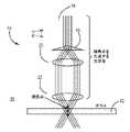
これに対して、本明細書に記載の焦線レーザおよび短パルスレーザ処理は、延伸焦点または線焦点を生成する光学系を採用する。そのような線焦点を生成するように適合した光学システム10の例を図1に示す。 In contrast, the focused laser and short pulse laser processing described herein employs an optical system that produces a stretch focus or a line focus. An example of an
ここで図1を参照すると、ガラス基体などの基体12を、レーザビーム14を用いて処理するように適合した例示的な光学システム10を概略的に示している。システム10において、例えば、光学システム10は、レーザビーム14について、基体12上に線焦点16を生成するように適合している。レーザビーム14の線焦点16を、基体12を欠陥部または穿孔の境界部または周縁部に沿って切断すること、および/または、基体12内に、第2群の欠陥部の境界部または周縁部の内側に配置された第1群の欠陥部を生成することを、可能にするように向いた欠陥部および穿孔(例えば、上記第2群の欠陥部)を生成するように適合しうる。 Here, with reference to FIG. 1, an exemplary
光学システム10は、レーザビーム14(例えば、パルス状レーザビーム)を、ビーム伝播方向に沿って向いたレーザビーム焦線16に集光するように適合している。基体12(例えば、ガラス基体シート)は、吸収が、レーザの波長で、材料の厚さ1mm当たり約10%未満の場合、いくつかの例においては、材料の厚さ1mm当たり約1%未満の場合、この波長に対して実質的に透明である。図1に示すように、レーザは、光学アセンブリ10に入射する部分を有するレーザビーム14を出射する。光学アセンブリ10は、入射したレーザビームの向きを変えて、ビーム方向に沿って画定された拡張範囲に亘り、光学システム10の出射側の延伸レーザビーム焦線16に向ける。平坦な基体12(例えば、ガラス基体シート)を、ビーム経路に配置して、少なく部分的に、レーザビーム14のレーザビーム焦線16と重なるようにする。したがって、レーザビーム焦線16を、基体12内に向けることになる。 The
一実施形態において、例えば、レーザからの入射したガウシアンビームは、線焦点を生成するアキシコン18(円錐形光学要素)を通り抜ける。線焦点は、それを他の位置に投射して、その空間的広がりも変えるために、望遠鏡を形成するレンズなどの他の標準的な光学要素を通り抜けて、伝播するか、像を再形成しうる。これは、ベッセルビーム、または、より具体的には、ガウシアンベッセルビームを生成すると称することもある。そのようなビームは、ガウシアンビームより非常にゆっくりと回折して、非常に高い光強度の中心領域(直径が略数マイクロメートル)を、非常に長い範囲で(略ミリメートル領域で)維持するのを可能にする。広義では、非回折ビームと称することが多い、延伸した線焦点を形成する他の解決策も可能である。 In one embodiment, for example, an incident Gaussian beam from a laser passes through an axicon 18 (conical optical element) that produces a line focus. The line focus propagates or reshapes the image through other standard optics, such as the lens that forms the telescope, to project it to another location and also change its spatial extent. sell. This may also be referred to as producing a Bessel beam, or more specifically a Gaussian Bessel beam. Such a beam diffracts much more slowly than a Gaussian beam, maintaining a very high light intensity central region (approximately a few micrometers in diameter) over a very long range (approximately in the millimeter region). to enable. In a broad sense, other solutions that form a stretched line focus, often referred to as non-diffraction beams, are also possible.
図1に示した特定の実施形態において、例えば、アキシコン18は、光学アセンブリ10に入射するレーザビーム14の少なくとも一部を、第1レンズ20に向けて分散する。第1レンズ20は、光学アセンブリ10内で、分散したレーザビーム14を平行光にして第2レンズ22に向ける。第2レンズ22は、レーザビーム14の平行光部分を受光して、ビーム14を基体12に向けて集光して、ビームをレーザビーム焦線16内に集光する。 In the particular embodiment shown in FIG. 1, for example, the
一実施形態において、線焦点を、非常に高パルスエネルギーの短パルス状レーザ(例えば、パルス幅が10ps未満で、約50から500μJ/バースト)と共に用いる。多くの短パルスレーザは、「バースト」パルスモードと称する動作モードを可能にする。「バースト」パルスは、時間的に接近した間隔の一連のパルスであり(例えば、20ナノ秒)、一方、各「バースト」間の時間は、10ナノ秒など、もっと長くてもよい。各レーザ用の利得媒質は、短時間のスケールで抽出できる一定量のエネルギーを有し、典型的には、バースト内の全エネルギーが保たれ、つまり、レーザが一定周波数で動作すると、2つのパルスバースト内の全エネルギーは、6つのパルスバースト内の全エネルギーと同じになる。各パルスを、線へと集光して、非線形吸収プロセスを介して、ガラス内に線状欠陥部を生成する。この実施形態において、基体は、照射に対して実質的に透明であり(典型的には、1mm当たり<10%の吸収)、そうでないと、エネルギーは、ガラスの表面で、または、その近くで吸収されてしまい、内部に達して線を形成しないだろう。しかしながら、完全な貫通孔を必要としない他の実施形態において、透明性がもっと低い基体も用いてもよい。一実施形態において、レーザの波長は、約1064nmであり、それは、Nd:YV04レーザ、または、同様の(例えば、YAG)利得材料によって生成できる。更に、約532nm(2倍の周波数)、または、約355nm(3倍の周波数)など、この波長の様々な高調波も用いてもよい。これらの高調波は、レーザヘッドの出射部で非線形変換結晶を採用することによって容易に得られる。In one embodiment, the line focus is used with a short pulsed laser with very high pulse energy (eg, pulse width less than 10 ps, about 50 to 500 μJ / burst). Many short pulsed lasers allow for a mode of operation called "burst" pulse mode. A "burst" pulse is a series of pulses that are closely spaced in time (eg, 20 nanoseconds), while the time between each "burst" may be longer, such as 10 nanoseconds. The gain medium for each laser has a certain amount of energy that can be extracted on a short scale, typically keeping all the energy in the burst, i.e., two pulses when the laser operates at a constant frequency. The total energy in the burst will be the same as the total energy in the six pulse bursts. Each pulse is focused into a line to create a linear defect in the glass via a non-linear absorption process. In this embodiment, the substrate is substantially transparent to irradiation (typically <10% absorption per mm), otherwise the energy is on or near the surface of the glass. It will be absorbed and will not reach the inside and form a line. However, in other embodiments that do not require a complete through hole, a less transparent substrate may also be used. In one embodiment, the wavelength of the laser is about 1064 nm, which can be produced by an Nd:YV04 laser or a similar (eg, YAG) gain material. Further, various harmonics of this wavelength may also be used, such as about 532 nm (double frequency) or about 355 nm (triple frequency). These harmonics can be easily obtained by adopting a non-linear conversion crystal at the emission part of the laser head.
透明基体における結果は、紙を穿孔する効果に非常に近い。穿孔は、非常に少量の材料を除去するが、亀裂、または、割れ目を誘導して、最終的には基体を分離するすることができる。これらの欠陥部が互いに接近した間隔の場合には、割れ目が形成されて、欠陥部を互いに接続する。このプロセスの1つの利点は、非常に少量の材料を除去するので、非常に少量の破片を生成するということである。 The results on transparent substrates are very close to the effect of perforating paper. Perforation removes a very small amount of material, but can induce cracks or crevices and ultimately separate the substrate. When these defective parts are close to each other, a crack is formed to connect the defective parts to each other. One advantage of this process is that it removes very small amounts of material, thus producing very small amounts of debris.
多くのイオン交換ガラスの場合のように、基体が内部に十分な応力を有すると、割れ目は、更なる処理を必要とせずに、1つの欠陥部位置から他の欠陥部位置へ伝播するだろう。しかしながら、コーニング社のEagle XGなどの表示装置用ガラスまたはイオン交換前ガラスの場合のように、基体が低い応力を有する場合には、次に、更なる応力を加えて、損傷位置間に割れ目を完全に形成することができる。一実施形態において、例えば、この処理は、二酸化炭素(CO2)レーザなどの赤外線レーザを用いて、同じ穿孔(欠陥)パターンを辿ることによって行うことができる。これにより、割れ目の伝播を高める熱応力を生じて、結果的に、2つの部分に分離する。図4は、欠陥部が形成されているが、分離していないガラスの画像を示している。図5は、結果的に得られる、分離後の縁部の画像を示している。If the substrate has sufficient internal stress, as in many ion exchange glasses, the crevices will propagate from one defect location to another without the need for further treatment. .. However, if the substrate has low stress, as in the case of display glass or pre-ion exchange glass such as Corning's Eagle XG, then additional stress is applied to create cracks between the damaged locations. Can be completely formed. In one embodiment, for example, this treatment can be performed by following the same perforation (defect) pattern using an infrared laser such as a carbon dioxide (CO2 ) laser. This creates a thermal stress that enhances the propagation of the cracks, resulting in separation into two parts. FIG. 4 shows an image of glass in which defects are formed but not separated. FIG. 5 shows the resulting image of the edge after separation.
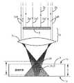
図2Aおよび2Bを参照すると、材料をレーザ処理する光学システムおよび方法の他の実施形態は、パルス状レーザビーム2を、ビーム伝播方向に沿った向きのレーザビーム焦線2bに集光する工程を含む。吸収が、レーザの波長で材料の深さ1mm当たり約10%未満、好ましくは、約1%未満の場合に、基体1(例えば、ガラス基体シート)は、この波長に対して実質的に透明である。図2Aに示すように、レーザ(不図示)は、光学アセンブリ6に入射する部分2aを有するレーザビーム2を出射する。光学アセンブリ6は、入射レーザビームを、ビーム方向に沿って画定された拡大範囲に亘る(長さlの焦線)、光学アセンブリ6の出射側の延伸レーザビーム焦線2bに向ける。平坦な基体1は、ビーム経路内に位置して、少なくとも部分的に、レーザビーム2のレーザビーム焦線2bと重なる。したがって、レーザビーム焦線は、基体内に向けられる。参照符号1aは、光学アセンブリ6またはレーザと向い合う平坦な基体の表面を指し、参照符号1bは、基体1の反対側の面を指す。基体または材料の(この実施形態において、平面1aおよび1bに、つまり、基体平面に垂直に測定した)厚さは、dと符号を付している。 Referring to FIGS. 2A and 2B, another embodiment of an optical system and method of laser processing a material comprises the step of condensing the
図2Aに示したように、基体1を、ビームの長軸に垂直に、したがって、光学アセンブリ6によって生成された同じ焦線2bの後ろ側に位置合わせする(基体は、描画平面に垂直である)。焦線を、ビーム方向に沿って向けるか、位置合わせして、焦線2bが基体の表面1aの前で始まり基体の表面1bの前で止まるように、つまり、焦線2bは基体内で終端して表面1bを越えて延伸しないように、基体を焦線2bに対し位置決めする。レーザビーム焦線2bが基体と重なる領域において、つまり、焦線2bに重なる基体材料中で、(レーザビーム2を、長さlの部分、つまり、長さlの線焦点上に集光することによって確保される強度である、レーザビーム焦線2bに沿った適切なレーザ強度だと仮定すると、)延伸レーザビーム焦線2bは、(レーザビームの長軸に沿って位置合わせされた)延伸部分2cを生成し、それに沿って基体材料中に誘起吸収を生じる。誘起吸収は、部分2cに沿って、基体材料中に欠陥線を形成する。欠陥線は、1つの高エネルギーバーストパルスを用いた、基体内の微細な(例えば、直径が、>100nm、かつ、<0.5マイクロメートル)細長い「孔」(穿孔または欠陥線とも称する)である。個々の欠陥線を、例えば、数百キロヘルツの速度で(毎秒数十万の欠陥線で)生成できる。レーザ源と基体間の相対的な動きにより、これらの孔を互いに隣接して、(マイクロメートル未満から数マイクロメートルまで変動して空間的に分離し)配置できる。欠陥線形成は、局所的なだけではなく、誘起吸収の延伸部分2cの全長に亘る。(レーザビーム焦線2bが基体1と重なる部分の長さに対応する)部分2cの長さには、符号Lが付されている。誘起吸収部分2cの平均直径または範囲(または、基体1の材料中の欠陥線形成を受けた部分)には、符号Dを付している。この平均範囲Dは、基本的にレーザビーム焦線2bの平均直径δ、つまり、約0.1マイクロメートルと約5マイクロメートルの間の範囲の平均スポット直径に対応する。 As shown in FIG. 2A, the
図2Aに示すように、(レ―ザビーム2の波長λに対し透明な)基体材料は、焦線2b内のレーザビームの高い強度に関連した非線形効果に起因する焦線2bに沿った誘起吸収によって、加熱される。図2Bは、対応する誘起張力が微細な割れ目形成につながるように、張力が表面1aで最も高い状態で、加熱された基体材料が最終的に膨張するのを示している。 As shown in FIG. 2A, the substrate material (transparent to the wavelength λ of the laser beam 2) is induced absorption along the
レーザ源の選択は、透明材料中に多光子吸収(MPA)を生じる能力に基づく。MPAは、分子を、1つの状態(通常、基底状態)から、より高エネルギー電子状態(イオン化)へ励起させるための同一または異なる周波数の2つ以上の光子の同時吸収である。関わる分子のエネルギーがより低い状態とより高い状態との差は、2つ以上の光子のエネルギーの合計に等しくなりうる。誘起吸収とも称するMPAは、例えば、線形吸収より数桁弱い、三次のプロセスでありうる。MPAは、例えば、誘起吸収の強度が、光強度自体に比例ではなく、光強度の二乗または三乗に比例しうる点で、線形吸収と異なる。したがって、MPAは、非線形の光学プロセスである。 The choice of laser source is based on the ability to produce two-photon absorption (MPA) in the transparent material. MPA is the simultaneous absorption of two or more photons of the same or different frequencies to excite a molecule from one state (usually the ground state) to a higher energy electronic state (ionization). The difference between the lower and higher energies of the molecules involved can be equal to the sum of the energies of two or more photons. MPA, also referred to as induced absorption, can be, for example, a tertiary process that is orders of magnitude weaker than linear absorption. MPA differs from linear absorption in that, for example, the intensity of induced absorption can be proportional to the square or cube of the light intensity rather than the light intensity itself. Therefore, MPA is a non-linear optical process.
焦線2bを生成するのに適用しうる代表的な光学アセンブリ6、および、これらの光学アセンブリを適用しうる代表的な光学機構を、以下に記載する。同一の構成要素または特徴物、若しくは、等しい機能の構成要素または特徴物には、同一の参照符号を用いている。 Representative
図2Aに示した実施形態において、必要な開口数を実現するために、光学系は、一方では、公知のアッベ式(N.A.=n sin(シータ)、n:加工されるガラスまたは他の材料の屈折率、シータ:開口角の半分、更に、シータ=arctan(D/2f)、D:口径、および、f:焦点距離)による、所定の焦点距離に必要な開口を有さなければならない。他方では、レーザビームは、光学系を必要な口径まで照射しなければならず、典型的には、レーザと集光光学系との間に拡大望遠鏡を用いてビームを広げることによって実現する。 In the embodiment shown in FIG. 2A, in order to achieve the required numerical aperture, the optical system is, on the one hand, a known Abbe formula (NA = n sin (theta), n: glass to be processed or the like or the like. The index of refraction of the material, theta: half the aperture angle, and theta = arctan (D / 2f), D: caliber, and f: focal length) must have the necessary aperture for the given focal length. It doesn't become. On the other hand, the laser beam must illuminate the optical system to the required aperture and is typically achieved by spreading the beam between the laser and the focused optical system using a magnifying telescope.
スポットの大きさの変化は、焦線に沿った均一な相互作用のために、強すぎるべきでない。これは、例えば、ビーム開口、したがって、開口数の割合が僅かだけ変化するように、小さい円形領域だけの集光光学系を照射することによって確実にできる(以下の実施形態を参照)。 The change in spot size should not be too strong due to the uniform interaction along the focus. This can be ensured, for example, by irradiating the focused optical system with only a small circular region so that the beam aperture, and thus the proportion of the numerical aperture, varies only slightly (see embodiments below).
図3によれば(レーザ放射2のレーザビーム光束における中心ビームのレベルで基体平面に対して垂直な部分;ここでも、レーザビーム2は基体平面に垂直に入射し、つまり、焦線2bまたは誘起吸収2cの延伸部分が基体の垂線に平行となるように入射角は0°)、レーザによって出射したレーザ放射光2aは、最初に、使用したレーザ放射光に対して完全に不透明な円形の開口部8に向けられる。開口部8は、ビームの縦軸に垂直に向き、図示したビーム光束2aの中心ビームに中心が合わせられる。開口部8の直径を、ビーム光束2aの中心付近のビーム光束、または、中心ビーム(ここでは2aZと符号を付した)が開口部に当たって開口部によって完全に吸収されるように、選択する。ビーム光束2aの外縁範囲内のビーム(ここでは2aRと符号を付した周辺光線)だけは、開口部の大きさがビーム直径と比べて小さいので吸収されずに、開口部8の横を通過して、本実施形態では、球面状に切断した両凸レンズ7として設計している光学アセンブリ6の集光光学要素の、周辺領域に当たる。 According to FIG. 3 (the portion of the laser beam beam of the
図3に示したように、レーザビーム焦線2bは、レーザビームについての単一の焦点のみでなく、むしろ、レーザビーム内の異なる光線についての一連の焦点である。この一連の焦点は、図3に長さlのレーザビーム焦線2bとして示した、画定された長さの細長い焦線を形成する。レンズ7は中心ビームに中心が合わせられ、本実施形態において、補正していない両凸集光レンズとして、一般的な球面状に切断したレンズの形状で設計している。このようなレンズの球面収差は有利であり得る。その代わりに、理想的な焦点を形成しないが、画定した長さの明確な細長い焦線を形成する、理想的に補正した系から逸脱した非球面レンズ系または多レンズ系(即ち、単一の焦点を持たないレンズまたは系)も用いることができる。従って、レンズのゾーンは、レンズ中心からの距離に応じて焦線2bに沿って集光する。ビーム方向を横断する開口部8の直径は、(ビーム強度がピーク強度の1/e2まで減少するのに必要な距離によって画定される)ビーム光束の直径の約90%であり、光学アセンブリ6のレンズの直径の約75%である。従って、収差補正していない球面レンズ7の、中心においてビーム光束を遮断することによって生じる焦線2bを用いる。図3は、中心ビームを通る1つの平面における断面を示しており、図示したビームを焦線2bの周りに回転すると、完全な三次元光束を見ることができる。As shown in FIG. 3, the
少なくとも1つの表面1a、1bが焦線に重なるように焦線2bを配置して、誘起吸収2cの部分が、基体の少なくとも1つの表面上で始まるようにすることは、利点があるかもしれない。 It may be advantageous to arrange the
米国特許出願公開第2015/0166396号明細書に開示された、基体に孔をあけるためにレーザ焦線を生成する更なる実施形態を利用してもよい。更に、レーザ焦線を用いない他のレーザ穴あけ方法も利用してもよいと理解すべきである。 Further embodiments disclosed in U.S. Patent Application Publication No. 2015/0166396 may be used to generate laser focus lines for drilling holes in the substrate. Furthermore, it should be understood that other laser drilling methods that do not use laser focus may also be used.
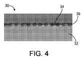
図4は、レーザによって形成した欠陥部36または穿孔をつなぐ割れ目34を示す、基体32の例示的な顕微鏡画像30を示している。割れ目34、および、レーザで形成された欠陥部を用いて、基体32を切断または傷付けてもよい。一実施形態において、例えば、ガラス基体の欠陥部間のピッチは、10μm未満でもよいが、他の寸法も想定され、任意の所定の基体の特徴に応じて変わりうる。欠陥部36または穿孔は、例えば、望ましい形状のコンポーネントの周りの閉じた境界部または周縁部に概して配置されて、上記第2群の欠陥部を提供して、基体32を切断または傷付けて、1つ以上のコンポーネントにしてもよい。例えば、閉じた境界部は、第2群の欠陥部、および、それらをつなぐ割れ目によって全体的に形成した閉じた境界部を含むか、第2群の欠陥部と、全基体32の1つ以上の縁部との組合せによって形成し、基体から形成されたコンポーネントは、全基体32と共通の縁部を含んでもよい。 FIG. 4 shows an exemplary
図5は、本明細書に記載の1つ以上のレーザ線焦点切断プロセスの実施形態から結果的に得られる特徴的な縁部42を示す、例示的な走査型電子顕微鏡(SEM)画像40を示している。この特定の例において、一連の損傷跡または欠陥部44(例えば、境界部または周縁部を形成する第2群の欠陥部)が見え、各々が、上面46から底面48までガラス基体の全厚さを通って、ガラス基体から分離した縁部に、波形または鋸歯状のテクスチャを提供している。 FIG. 5 is an exemplary scanning electron microscope (SEM)
そのような波形の、または、穿孔された縁部は、独特の特徴を有する。目視すると、つや消し、または、軽く研磨した外観を有する。顕微鏡で見ると、線状欠陥部から生成された縞部によって容易に特徴付けられて、縁部に波形のテクスチャを提供する。これらの線状欠陥部のピッチは、縞部の間隔を決定する。ここでも、これらを、光学顕微鏡で容易に見ることができる。縁部は、切断片の内部に延伸する低い表面下損傷(例えば、典型的には、100マイクロメートル未満)、良好で非常に一貫した縁部強度(例えば、典型的には、100MPaより高く、150MPaより高いことが多く、ばらつきは、10MPa未満であることが多い)、および、90度の輪郭を含む、多くの望ましい特性を有する。 Such corrugated or perforated edges have unique characteristics. Visually, it has a matte or lightly polished appearance. When viewed under a microscope, it is easily characterized by streaks generated from linear defects, providing a corrugated texture at the edges. The pitch of these linear defects determines the spacing between the streaks. Again, these can be easily seen with a light microscope. The edges have low subsurface damage extending into the cut pieces (eg, typically less than 100 micrometers), good and highly consistent edge strength (eg, typically above 100 MPa). Often above 150 MPa, the variability is often less than 10 MPa), and has many desirable properties, including a 90 degree contour.
これらの穿孔が、もっと大きく間隔をあけると(例えば、20マイクロメートル以上)、(基体によっては)互いの間をつなぐ割れ目を形成しない。図6において、例示的なSEM画像50は、レーザビームがガラスに入射する位置で、欠陥部または穿孔がどう見えるかを示している。これらの欠陥部または損傷跡(または、案内孔)は、非常に小さく、350nm程度の直径である。これらの欠陥部を、化学エッチングによる更なる処理を用いた拡大して、マイクロメートル領域の大きさの孔を生成しうる。図7は、エッチング前と後の両方のそのような穿孔または孔の側断面図を示している。そのようなエッチングは、5%のHF/10%のHNO3溶液などの酸性混合物、若しくは、KOHまたはNaOHなどの塩基性溶液を用いて行いうる。全ての場合において、エッチング液は、レーザによって形成した損傷跡に優先的に浸透して、エッチング液に対する露出時間の関数として、損傷跡が放射状に広がるのを可能にする。When these perforations are more spaced (eg, 20 micrometers or more), they do not form a fissure that connects them (depending on the substrate). In FIG. 6, the
図6は、本明細書に記載の1つ以上のレーザ線焦点切断工程などによって形成してもよい、ガラス基体56内の個々の欠陥部54の入射側52の例示的なSEM画像50を示している。例えば、欠陥部54は、基体内に形成した第1群の欠陥部の1つに対応して、孔、ビア、インターポーザなどを、他の欠陥部または穿孔(例えば、第2群の欠陥部)の周縁部内に提供してもよい。この例示的なSEM画像50において、例えば、個々の欠陥部54は、基体56の入射側52から基体56内に延伸する開口孔またはチャネル58を含む。この特定の例において、チャネル58は、約350nmである。 FIG. 6 shows an
図7は、例示的なエッチング前60およびエッチング後70のガラス基体62のSEM画像を示している。この特定の例において、エッチング前の画像60は、焦線レーザ方法によって基体62(本実施形態においては、コーニング社が販売する、厚さが300μmのEagle XG(EXG)ガラス基体)内に作られた複数の焦線レーザ穿孔64を示している。エッチング前のSEM画像60は、1片のガラス基体62の裂いた縁部66を通して見たものである。この特定の実施形態において、穿孔/孔64は、ガラス基体62の縁部66から約200μm内側に位置して、基体の全厚さを通して延伸している。図7は、機械的に清浄した縁部66の非平坦面からの画像の僅かな歪みを示している。エッチング後のSEM画像70は、HFとHNO3の混合物によるウェットエッチングを用いて直径を約50μmに拡大した、同じ穿孔64’を示している。線焦点レーザビームを、基体に対して非常に高く、または、低く位置させて、基体の全厚さに延伸するものではないブラインドホールを形成することも可能である。これらの孔を上記と同様にエッチングして、金属被覆などの下流側処理において好まれることもあるブラインドビアを形成しうる。FIG. 7 shows SEM images of the
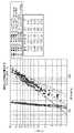
更に、最終的な開口孔の直径とするために案内孔をエッチングするので、切断縁部の強度も高めることになる。図8は、厚さ130μmのEXGガラスについて、2点曲げ試験方法を用いて、結果的に得られる縁部強度のワイブルプロットを示している。切断した状態で、ガラス部品の縁部の強度は、約145MPaのB10値を有し、データは、この切断方法の特徴である、非常に一貫した縁部を示す非常に急峻な傾きを有する。酸エッチング後に、切断工程により存在する損傷部のいくつかの除去、および、ガラス内の亀裂または割れ目を、酸で丸まった角にすることにより、縁部の強度は高まる。これにより、インターポーザ用の孔を生成するのに概して必要な最低エッチング量である、わずか10μm以上のエッチング後に、結果的にB10縁部強度値は約300~400MPaになる。そのような強度は、純粋に機械的な切断および縁部研削方法によって製作したウェハの典型的な縁部強度より非常に高く、レーザ切断した部品に酸エッチングを加えることで、典型的な下流側処理で必要な縁部強度を超えることを意味する。 Further, since the guide hole is etched to obtain the diameter of the final opening hole, the strength of the cut edge portion is also increased. FIG. 8 shows a Weibull plot of the resulting edge strength of an EXG glass with a thickness of 130 μm using a two-point bending test method. In the cut state, the strength of the edge of the glass part has a B10 value of about 145 MPa and the data have a very steep slope showing a very consistent edge, which is characteristic of this cutting method. After acid etching, the strength of the edges is increased by removing some of the damaged parts present by the cutting process and by making the cracks or crevices in the glass into acid rounded corners. As a result, the B10 edge strength value becomes about 300 to 400 MPa after etching of only 10 μm or more, which is the minimum etching amount generally required to generate a hole for an interposer. Such strength is much higher than the typical edge strength of wafers made by purely mechanical cutting and edge grinding methods, and by applying acid etching to laser cut parts, the typical downstream side. It means that the edge strength required for the treatment is exceeded.
ガラスの切断は、多数の調節可能なパラメータを伴う。最も重要なのは、レーザパラメータであり、レーザ繰返し周波数(kHz)、バースト数(B)、パルスエネルギー(μJ)、最終対物レンズの焦点距離によって制御することが多い線焦点の長さ、および、基体に対する焦点位置を含む。パルスエネルギー、および、基体に穿孔を生成するプロセスの速度は、周波数に直接的に関係している。バースト数は、レーザと材料との相互作用の強度に、したがって、欠陥部の周りに形成される微細な割れ目の度合いに影響を与えるのに有用である。本明細書において、微細な割れ目という用語は、基体内に欠陥部の略中心から形成される放射状の割れ目を称する。微細な割れ目は、約20μm以下で、基体の厚さを全て貫通しても、そうでなくてもよい。欠陥部を用いて、基体を切断または切り目を入れる際に、微細な割れ目は、基体を弱くすることによって、促進される。 Cutting glass involves a number of adjustable parameters. The most important are the laser parameters, which are often controlled by the laser repetition frequency (kHz), burst number (B), pulse energy (μJ), focal length of the final objective, and the substrate. Includes focal length. The pulse energy and the speed of the process of creating perforations in the substrate are directly related to frequency. The number of bursts is useful in influencing the intensity of the laser-material interaction and, therefore, the degree of fine cracks formed around the defect. As used herein, the term fine crevice refers to a radial crevice formed in the substrate from approximately the center of the defect. The fine cracks are about 20 μm or less and may or may not penetrate the entire thickness of the substrate. Fine cracks are promoted by weakening the substrate when cutting or making cuts in the substrate using the defective portion.
パルスエネルギーの閾値は、基体に応じて材料を改質するのに必要であり、欠陥部の周りに形成される割れ目の度合いに影響する。光送達部で用いる最終対物レンズは、線焦点の長さ、および、エネルギー密度を変える。最後のパラメータは、任意の穿孔をつなげて部品輪郭の形成に影響する欠陥部間のピッチであり、レーザのトリガーとステージの移動の関係によって決定する。 The pulse energy threshold is required to modify the material depending on the substrate and affects the degree of cracks formed around the defect. The final objective lens used in the optical delivery unit changes the length of the line focus and the energy density. The final parameter is the pitch between the defects that connect any perforations and affect the formation of the contour of the part, which is determined by the relationship between the laser trigger and the stage movement.
ガラス基体の切断について、表1に示した、以下の穿孔パラメータは、切断した際の良好な縁部強度(100MPaより高い)と共に、切断部品の一貫した分離を行うことを見出した。NIXは、イオン交換前にレーザ処理したガラスを示し、IOXは、同じガラスであるが、イオン交換後にレーザで処理したものを示し、2318および2319は、2つのタイプのイオン交換可能ガラスについてのコーニング社のガラス組成コードを示す。 For cutting glass substrates, the following drilling parameters shown in Table 1 have been found to provide consistent separation of the cut parts, along with good edge strength (higher than 100 MPa) when cut. NIX indicates glass that has been laser treated before ion exchange, IOX indicates the same glass but laser treated after ion exchange, and 2318 and 2319 are Corning for two types of ion exchangeable glass. The glass composition code of the company is shown.

表1に示した上記条件は、上記材料を切断するのに用いてもよい全ての可能なパラメータ範囲を示すのではなく、一貫した部品切断、次のCO2レーザの利用による容易な分離、および、良好な縁部強度について良好な結果を生じる、例示的なパラメータを示している。The above conditions shown in Table 1 do not indicate all possible parameter ranges that may be used to cut the material, but consistent part cutting, easy separation by the use of the next CO2 laser, and , Shows exemplary parameters that give good results for good edge strength.
CO2レーザによる分離について、約50から100Wのレーザパワーを、ガラスにおいて、直径が約2から6mmのスポットに集光することは、予め穿孔した輪郭を、約100から250mm/秒の速度で分離するのに十分であることを見出した。全ての場合において、望ましい分離速度と、集光スポットの大きさと、レーザパワーとの間にはトレードオフの関係がある。より速い分離速度にするには、より高いレーザパワーを用い、より大きいスポット直径にするには、より高いレーザパワーも用いうる。より遅い分離速度にするには、レーザパワーを低下させるか、および/または、スポットの大きさを大きくして、ガラス表面の熱によるアブレーションを回避しうる。For separation by CO2 laser, condensing a laser power of about 50 to 100 W onto a spot with a diameter of about 2 to 6 mm on glass separates pre-drilled contours at a rate of about 100 to 250 mm / sec. Found to be enough to do. In all cases, there is a trade-off between the desired separation rate, the size of the focused spot, and the laser power. Higher laser powers can be used for faster separation rates and higher laser powers can be used for larger spot diameters. For slower separation rates, the laser power may be reduced and / or the spot size may be increased to avoid thermal ablation of the glass surface.
表1の最後の場合(IOX2319)において、ガラスは、既にイオン交換されているので、かなりの引っ張り応力を有しており、輪郭を穿孔すると直ちに分離し、従って、分離するのにCO2熱曝露を必要としない。In the last case of Table 1 (IOX2319), the glass has significant tensile stress because it has already been ion-exchanged and separates immediately upon drilling the contour, thus being exposed to CO2 heat to separate. Does not need.
ガラスの穴あけについて良好な結果を得るには、金属被覆工程には丸い(円形の)孔が概して望ましく、部品の強度および信頼性を高めるか、または、最高にするためには、材料の微細な割れを減少または最小にすべきである。従って、強い損傷跡を基体を通って作って、結果的にエッチング液の通り易い経路を提供することに対し、材料に大きすぎる損傷を生じさせて、非理想的な孔形状を生成することとは、互いにトレードオフの関係がある。図9は、厚さ300μmのEXGガラスについてプロセスを検討した結果を示し、パルスエネルギー、および、最終対物レンズの焦点距離を変えて、これらの効果を示している。画像は、エッチング後の孔の上面図および側面図を示している。この実験について、100%のパワーは、1バースト当たり約185μJのエネルギーに対応し、全条件は、1バースト当たり2パルスにおけるものであった。線焦点の長さは、レンズAについては約1.3mmであり、レンズBについては約1.8mmであり、レンズCについては約2.5mmだった。最小焦点距離、および、最高パルスエネルギーについて、エッチングにより長円の特徴物になった孔の周りに放射状の割れ目が形成されて、最上部の画像のような楕円状の孔が生成された(例えば、レンズA、100%パワー)。最低のパルスエネルギーでは、材料を通る損傷跡は、エッチング液の急速な浸透を可能にするには十分強くなく、エッチング後に、真の貫通孔は観察されない(例えば、レンズC、50%パワー)。図10は、結果をまとめて示している。最良の妥協条件を、緑で示しており、パワー(パルスエネルギー)が閾値より僅かに高く保たれて、材料を損傷するが、エッチングで長円の孔になる大きい放射状の割れ目を形成するには、十分には高くない。概して、最も長い線焦点の長さについて、最も幅広の処理領域が観察された(レンズC)。 Round (circular) holes are generally desirable for metal coating processes to obtain good results for glass drilling, and the fineness of the material is to increase or maximize the strength and reliability of the part. Cracks should be reduced or minimized. Thus, while creating strong damage marks through the substrate, resulting in an easy path for the etchant, it causes too much damage to the material and creates a non-ideal pore shape. Have a trade-off relationship with each other. FIG. 9 shows the result of examining the process for EXG glass having a thickness of 300 μm, and shows these effects by changing the pulse energy and the focal length of the final objective lens. The image shows a top view and a side view of the holes after etching. For this experiment, 100% power corresponded to about 185 μJ of energy per burst and all conditions were at 2 pulses per burst. The length of the line focal point was about 1.3 mm for the lens A, about 1.8 mm for the lens B, and about 2.5 mm for the lens C. For the minimum focal length and maximum pulse energy, etching created radial fissures around the holes featured in the oval, creating elliptical holes like the top image (eg, top image). , Lens A, 100% power). At the lowest pulse energy, the damage marks through the material are not strong enough to allow rapid penetration of the etchant and no true through-holes are observed after etching (eg lens C, 50% power). FIG. 10 summarizes the results. The best compromise is shown in green, where the power (pulse energy) is kept slightly above the threshold, damaging the material, but to form large radial crevices that result in oval holes in the etching. , Not high enough. In general, the widest processing area was observed for the longest line focal length (lens C).
同様の結果が、コーニング社のコード2318または2319ガラスなどの他の材料についても観察された。従って、穴あけ/穿孔について、いくつかの良好な条件を、以下の表2に示す。 Similar results were observed for other materials such as Corning Code 2318 or 2319 glass. Therefore, some good conditions for drilling / drilling are shown in Table 2 below.

上記処理条件を用いて、厚さ0.7mmのコーニング社のコード2318ガラスで作られたウェハの切断および穴あけを実施した。プロセスは、以下の通りだった。
1.300×300mmのガラスシートを、機械に載置した。
2.200mmのウェハの輪郭を、放出線に沿って穿孔し、余分なガラス片の除去を容易にした。
3.CO2レーザを用いて、穿孔した輪郭を分離した。
4.中心の孔パターンを、穿孔により露出した。Using the above processing conditions, a wafer made of Corning Code 2318 glass with a thickness of 0.7 mm was cut and drilled. The process was as follows.
1. A 300 x 300 mm glass sheet was placed on the machine.
2. The contour of the 200 mm wafer was perforated along the emission line to facilitate the removal of excess glass shards.
3. 3. A perforated contour was separated using a CO2 laser.
4. The central hole pattern was exposed by perforation.
切断、および、このウェハ内に320,000個の孔パターンのレーザ露光の両方を行った全時間は、5分未満だった。これは、ウェハを機械的に切断して、形状に研削しなければならない場合より、かなり速く、更に、切断を任意の大きさに行ってもよく、機械に供給するガラスの在庫は、100mmのウェハ、200mmのウェハ用などに、異なる在庫品を必要とせず、単に空の大きいシートでありうることを意味する。更に、ガラスウェハを、切断工程と穴あけ工程の間に、機械から降ろすことがなかったので、ウェハの切断縁部に対して孔パターンを配置する工程は、ステージの精度のみによって支配され、この例においては、約+/-5マイクロメートルだった。 The total time for both cutting and laser exposure of 320,000 hole patterns in this wafer was less than 5 minutes. This is much faster than if the wafer had to be mechanically cut and ground into a shape, and the cutting may be done to any size, and the stock of glass supplied to the machine is 100 mm. It does not require different stock items, such as for wafers, 200 mm wafers, etc., and simply means that it can be a large empty sheet. Furthermore, since the glass wafer was not removed from the machine between the cutting and drilling processes, the process of arranging the hole pattern with respect to the cutting edge of the wafer is dominated only by the accuracy of the stage, in this example. In, it was about +/- 5 micrometers.
他の厚さ、並びに、EXG、2319 NIOXガラス、および、post-IOXガラスなどのガラス組成物も、穿孔および分離処理条件を適切に調節して、切断および穴あけした。 Other thicknesses, as well as glass compositions such as EXG, 2319 NIOX glass, and post-IOX glass, were also cut and drilled with appropriate adjustment of drilling and separation treatment conditions.
上記実施例において、1つのピコ秒レーザ光学ヘッドを用いて、穿孔の切断と穴あけの両方を行ったが、これらの工程を、2つの光学ヘッドを用いて、同じ機械で、または、2つの異なる機械でさえ行うことも可能である。2つの異なる光学ヘッドを採用する利点は、僅かに異なる線焦点の長さが、切断工程と、穴あけ工程とに最適であり得ることであり、概して、切断工程については、ガラスの損傷が大きい方が、間をつなぐ割れ目の生成を容易にするので望ましく、一方、穴あけ工程については、損傷を最小にして、最終的なエッチング後の孔の輪郭が、できるだけ丸く滑らかにするのを確実にするのが望ましい。そのような場合には、図11に示したように、電気光学(偏光に基づく)スイッチ、偏光ビームスプリッタと組み合わせた機械的に作動または回転する波長板、若しくは、空気力学的または機械的に駆動されるミラーの動きを用いて、1つのレーザビーム源を2つの光学ヘッド間で切り換えてもよい。 In the above embodiment, one picosecond laser optical head was used to both cut and drill the perforations, but these steps were performed using two optical heads on the same machine or in two different ways. It can even be done by machine. The advantage of adopting two different optical heads is that slightly different line focal lengths can be optimal for the cutting process and the drilling process, and generally for the cutting process, the glass is more damaged. However, it is desirable because it facilitates the formation of interstitial crevices, while for the drilling process, the damage is minimized to ensure that the contour of the final etched hole is as round and smooth as possible. Is desirable. In such cases, as shown in FIG. 11, an electro-optical (polarization-based) switch, a mechanically actuated or rotating waveplate in combination with a polarization beam splitter, or aerodynamically or mechanically driven. One laser beam source may be switched between two optical heads by using the motion of the mirror to be split.
図11は、2つの光学ヘッド82、84を採用した例示的なレーザシステム80を、概略的に示している。この例示的な実施形態において、1つの光学ヘッド82を、切断に最適に構成し、第2の光学ヘッド84は、穴あけ/基体内に孔を形成するのに最適に構成してもよい。光学スイッチ86を用いて、プロセス内の任意の所定の時間に、どちらのヘッドを使うか選択してもよい。例えば、光学スイッチ86は、空気力学的に、または、機械的に作動するミラー、偏光ビームスプリッタと組み合わした回転可能な波長板、または、他の光学要素、若しくは、偏光ビームスプリッタを通して送られる光の偏光状態に影響を与えることによって、レーザ88からのレーザビームの向きを変える電気光学スイッチを含んでもよい。 FIG. 11 schematically illustrates an
図12は、ガラスシート基体などの基体を切断および/または穴あけするのに、焦線レーザおよび/または短パルスレーザを用いて、基体を製作する例示的なプロセス200のフローチャートを示している。図12に示した実施形態において、動作202で、基体シートを担体に載置する。この実施形態において、例えば、システムは、ガラスまたは光送達部(または、それらの両方)を移動することによって、レーザをガラスに対し移動するステージを有する。図13~17を参照して、以下により詳しく記載するように、基体シートは、例えば、1枚以上の別々の基体シート、または、基体シート材料の連続したウェブ(例えば、システムの1つ以上のローラから供給する)を含んでもよい。動作204において、基体シートを、真空チャックなどを介して、担体に固定する。特定の第1群のレーザパラメータを、動作206で選択して、内側欠陥部(例えば、第1群の欠陥部)の望ましい形状、深さ、大きさ、または、他の特徴に対応する、1つ以上の特定の内側欠陥部を生成する。特定の第2群のレーザパラメータを、動作208で選択して、外側欠陥部(例えば、1つ以上の望ましい個々のコンポーネントの周りに境界部または周縁部を形成する第2群の欠陥部)の望ましい形状、深さ、大きさ、または、他の特徴に対応する、1つ以上の特定の外側欠陥部を生成する。動作210において、個々の形状を、CO2レーザを用いることなどにより、基体から分離する。動作212において、基体/分離した片を、真空チャックを解除することなどにより、担体から放出する。動作214において、基体シートから切断した担体および片を排出するか、他の方法でシステムから除去し、動作216において、自動および/または手動動作により、分離した片を担体から除去する。動作218において、担体を清浄して、破片を基体から除去し、再使用するように待ち列に配置する。図12に示した動作の順序は、例にすぎない。例えば、切断および穴あけ動作を、本明細書に記載したように、同じ、または、異なる装置で、どちらの順序で行ってもよい。更に、上記のように、特定の基体の特徴によっては、分離動作を追加のCO2レーザで行っても、行わなくてもよい。FIG. 12 shows a flow chart of an
焦線レーザ処理により、切断ガラス縁部の特性(強度、粗さ、表面下の損傷など)は、更に研削、面取り、および、研磨処理を行わずに、適切なものである。これにより、同じ製品を製造するための時間および費用を削減して、これらの処理による歩留まりの損失をなくす。更に、洗浄工程の回数を削減する。従来の工程については、ウェハを切断して、機械的な破片を除去するように研削した後に、洗浄工程が必要である。この工程を、上記の工程では除いてもよい。 By the focused laser treatment, the properties of the cut glass edge (strength, roughness, subsurface damage, etc.) are appropriate without further grinding, chamfering, and polishing. This reduces the time and cost of manufacturing the same product and eliminates yield losses due to these processes. Furthermore, the number of cleaning steps is reduced. For conventional steps, a cleaning step is required after cutting the wafer and grinding it to remove mechanical debris. This step may be excluded from the above steps.
同じシステムが、ガラスサンプルを切断および穴あけするので、いくつかの実施形態において、このことも、外側特徴物と孔パターン(例えば、インターポーザ孔)との間で位置の精度を大きく高めるという利点を有する。従来の方法では、機械的な切断および部品の縁部の研削の精度が低いので、部品の真の中心に対するパターン配置の全精度は、200μm程度である。ビジョンシステムを用いて、孔を穴あけする前に部品縁部を見つけるようにしても、誤差は大きくなりうる。これに対し、本明細書に記載のプロセスは、機械的に研削および研磨した部品と比べて、もっと非常に精密で高精度の外側寸法を有するレーザ処理した部品を、生成することができる。従って、切断および穴あけ工程が、時間の節約となるだけでなく、部品の仕様精度を大きく高めて、絶対許容誤差は約±5μmになる。 In some embodiments, this also has the advantage of greatly increasing the accuracy of the position between the outer feature and the hole pattern (eg, the interposer hole), as the same system cuts and drills the glass sample. .. In the conventional method, the accuracy of mechanical cutting and grinding of the edge of the part is low, so that the total accuracy of the pattern arrangement with respect to the true center of the part is about 200 μm. Even if the vision system is used to find the edge of the part before drilling a hole, the error can be large. In contrast, the process described herein can produce laser-treated parts with much more precise and precise outer dimensions than mechanically ground and polished parts. Therefore, the cutting and drilling process not only saves time, but also greatly enhances the specification accuracy of the component, resulting in an absolute tolerance of about ± 5 μm.
更に、薄いガラス(ガラス厚さ<200マイクロメートル)を処理する際の最大の困難点の1つは、手でのガラス取扱いである。ガラスは非常に薄いので、1枚の紙のような振舞いをする。このプロセスは、取扱いを削減し、したがって、薄いガラスの処理を可能にする。完全なシステムは、穴あけの前および後において、部品の手での取扱いを最小限にする。従来のシステムにおいて、部品を切断する時と、部品を穴あけシステムに載置し、次に、そこから取り除く時とに、部品を手で取り扱う。本願の工程では、取扱いは、システムから取り除く時だけであり、それは、自動化できる可能性もある。このことは、全体的な歩留まりの改善に直結する。 Furthermore, one of the biggest difficulties in processing thin glass (glass thickness <200 micrometers) is the handling of glass by hand. The glass is so thin that it behaves like a piece of paper. This process reduces handling and thus allows processing of thin glass. The complete system minimizes the manual handling of parts before and after drilling. In conventional systems, the parts are handled by hand when cutting the parts and when placing the parts in a drilling system and then removing them. In the process of this application, the handling is only when it is removed from the system, which may be automated. This directly leads to an improvement in overall yield.
大きいシートを処理して一連の個々の部品を製作する他の利点は、穴あけ工程の速度が、穴あけ処理自体の物理的過程ではなく、ビームをガラスに対して移動する速度によって、制限されるということである。ガラスを移動する工程を更に分解すると、ほとんどの時間が、加速および減速段階に使われる。多くの部品を同じパターンと組み合わせることによって、1つの部品当たりの実効時間を削減できる。パネル上で多くの部品を組み合わせることによって、レーザビームを大きいパネルに亘って走査する時の穴あけ速度を全体として高め、小さな部品だけを扱う時に必要な加速/減速の回数が少なくなる。 Another advantage of processing large sheets to make a series of individual parts is that the speed of the drilling process is limited by the speed at which the beam travels relative to the glass, not the physical process of the drilling process itself. That is. Further disassembling the process of moving the glass, most of the time is spent in the acceleration and deceleration stages. By combining many parts with the same pattern, the effective time per part can be reduced. By combining many components on the panel, the drilling speed as a whole when scanning the laser beam over a large panel is increased, and the number of accelerations / decelerations required when handling only small components is reduced.
図13および14は、多数のウェハ222、および、1つ以上の望ましいパターンを有するパネル224を、1つのより大きいパネル220から生成できることを示している。この場合、レーザ処理を用いて、孔パターン(例えば、案内孔、ビア、インターポーザなど)に対応する第1群の欠陥部を生成し、部品輪郭内の位置合わせ基準位置を含むウェハの輪郭を形成するなど、境界部または周縁部を形成する第2群の欠陥部を生成しうる。第2群の欠陥部のこの外側ウェハパターンを、別のレーザ工程(例えば、CO2レーザによる熱分離)を用いて放出するか、または、下流側の工程(酸エッチング)で放出しうる。利点は、各望ましい片を、任意の大きさ、および、寸法にし、各片が異なる内側の孔パターンを有することができることである。図13および14において、例えば、個々のウェハ222(図13)、および、個々のパネル224の外側の境界部または周縁部は、ウェハ222については概して円形の境界部または周縁部に、および、パネル224については概して矩形の境界部または周縁部に配置された第2群の欠陥部によって形成される。更に、第1群の欠陥部は、個々のウェハ222およびパネル224の境界部または周縁部内に配置して示した内側の孔(例えば、案内孔、ビア、インターポーザなど)を提供する。13 and 14 show that a large number of
図15は、例示的なレイアウトを示し、1枚のガラスシートを、4つの異なる大きさで、2つの異なるパターンに切断している。これは、ガラスの在庫管理を簡略にし、プロセスの用途を非常に広げるので、本明細書に記載の切断および穴あけ工程に特定の利点である。 FIG. 15 shows an exemplary layout in which one glass sheet is cut into two different patterns in four different sizes. This is a particular advantage to the cutting and drilling processes described herein, as it simplifies glass inventory management and greatly expands the use of the process.
例えば、図15に示すように、1枚の基体シート230において、1枚のパネル232、3つの300mmウェハ234、7つの150mmウェハ236、並びに、第1のパターンを有する2つの100mmのウェハ238、および、第2の別個のパターンを有する2つの100mmウェハ240を、同時に、1枚の基体シート230から穴あけできる。多くの個々のウェハまたはサブパネルを載置するのではなく、1枚の大きいガラスシートを載置して処理できる。図15において、例えば、個々のウェハ234、236、238および240、並びに、個々のパネル232の外側の境界部または周縁部を、ウェハ234、236、238および240については概して円形の境界部または周縁部に、および、パネル232については概して矩形の境界部または周縁部に配置された第2群の欠陥部によって形成する。更に、第1群の欠陥部は、個々のウェハおよびパネルの境界部または周縁部内に配置して示した内側の孔(例えば、案内孔、ビア、インターポーザなど)を提供する。 For example, as shown in FIG. 15, in one
これに対して、部品を所定の大きさに予め切断す場合には、様々な寸法のウェハの大量の在庫管理が必要となる。異なる販売業者用に、多くの異なる大きさ、および、厚さが必要なので、在庫は巨大になりうる。本明細書に記載のプロセスは、1つの大きさのマザーシートから、ウェハまたはパネルを切断して、多くの異なる大きさの在庫片を取得して、必要な在庫を削減し、単に異なる厚さのシート(または、スプール)を保有するという利点を有する。このことは、載置時間を削減し、部品の取扱い、および、トラッキングの複雑さを削減して、製造スループットを高める。 On the other hand, when the parts are pre-cut to a predetermined size, it is necessary to manage a large amount of wafers of various dimensions. Inventory can be huge because many different sizes and thicknesses are needed for different distributors. The process described herein cuts a wafer or panel from a mother sheet of one size to obtain many different sized pieces of stock, reducing the required stock and simply different thicknesses. Has the advantage of holding a sheet (or spool) of. This reduces mounting time, reduces component handling and tracking complexity, and increases manufacturing throughput.
図16は、望ましいパターンを有するウェハを含む多数のサブパネル252を、1枚のより大きいパネル250から生成できることを示している。この場合、レーザ処理を用いて、第1群の欠陥部などを介してインターポーザパターンを生成し、第1群の欠陥部の周りの境界部または周縁部を形成するように配置された第2群の欠陥部などを介して任意の位置合わせ基準位置を含むウェハ輪郭を生成しうる。更に、レーザ処理を用いて、サブパネル252を生成してもよい。このサブパネルパターンを、別のレーザ処理を用いて放出するか、酸エッチングなどの下流側処理で放出しうる。 FIG. 16 shows that a large number of
図17は、概略的に、供給材料を基体シート(例えば、コーニング社のWillowガラスなどのガラス基体)のスプールを介して供給する工程を示している。ロールを受け付ける能力は、材料の取扱い、および、ロールをパネルに変換する必要性を減少させる。レーザ処理アセンブリにおいて、システムは、切断、穴あけ、および、放出工程を行ってもよい。このシステムの出口側で、ピックアンドプレース装置を用いて、望ましい部品を搬出してもよい。 FIG. 17 schematically shows a step of supplying a feed material via a spool of a substrate sheet (eg, a glass substrate such as Corning's Willow glass). The ability to accept rolls reduces the handling of materials and the need to convert rolls into panels. In the laser processing assembly, the system may perform cutting, drilling, and emission steps. At the exit side of the system, a pick-and-place device may be used to unload the desired component.
図17を参照すると、レーザで基体シート302を製作するための例示的なプロセスおよびシステム300を、概略的に示している。概して、基体シート302を、処理前にスプール304で提供する。本明細書において、「基体シート」という用語は、ガラス基体シート、溶融シリカシート、サファイアシート、ガラス‐セラミック基体シート、または、セラミックシートを意味する。ガラス基体シートを、本明細書に記載したように、レーザで穴あけしてエッチングできる任意のガラス材料から製作してもよい。同様に、ガラス‐セラミック基体シート、および、セラミック基体シートを、本明細書に記載したように、レーザで穴あけしてエッチングできる任意のガラス‐セラミック、または、セラミック材料から製作してもよい。例示的なガラス組成物は、コーニング社のコード2318、2319および2320などの、コーニング社のEagle XGガラス、または、コーニング社のGorillaガラスの組成物であろう。特定のレーザに対し約20%未満の透過ロスを有するものなどの、部分的にセラミック化された材料を使用してもよい。 With reference to FIG. 17, an exemplary process and
上記のように、基体シート302に、レーザ穴あけ工程で穴をあけて、1つ以上の案内孔、ビア、インターポーザなどを提供するように適応した第1群の欠陥部、および、第1群の欠陥部を囲む境界部または周縁部に沿って配置された第2群の欠陥部または穿孔を、生成することができる。したがって、レーザ処理中に基体シート302を支持枠に固定する必要がないように、基体シート302は、最小の寸法変化で熱エネルギーを受け取ることができるべきである。例えば、典型的には高温の電子機器に利用されるポリイミドフィルムは、熱サイクルに曝されると、10μmから100μmの範囲の予想外の歪みを生じるかもしえない。比較すると、ガラス基体などの本明細書に記載の基体は、同じ熱サイクルに曝されても、検知可能な歪みを有さない。寸法上の安定性に加え、基体シート302は、約500°Cより高い温度に耐え、約50GPaより高いヤング率を有し、約3GPaより高い硬さを有すべきである。 As described above, the
基体シート302は、図17に示したように、スプールに巻き取ることができる厚さを有すべきである。限定するものではない例として、薄いガラス基体の場合には、基体シート302は、300μm未満の厚さを有してもよい。基体シート302は、材料の組成および特性に応じて他の厚さを有してもよいと理解すべきである。 The
図17に示すように、スプール304は、機械的に回転するスプールアセンブリ(番号を不付与)上に配置されて、基体シート302を巻き解く。このスプールアセンブリ、および、本明細書に記載の他のスプールアセンブリは、回転し、その上に巻き取った基体シート302を有することができる任意の装置として構成してもよい。 As shown in FIG. 17, the
図示した実施形態において、基体シート302は、スプール304から巻き解く時に、レーザ処理アセンブリ306を通過する。より詳細に以下に記載するように、レーザ処理アセンブリ306は、基体シート302を切断(例えば、第2群の欠陥部)、および/または、穴あけ(例えば、第1群の欠陥部)するために、基体シート302上、または、それに貫通して、複数の欠陥部(図17に不図示)をレーザで穴あけするように動作可能な1つ以上のレーザを含む。欠陥部は、以下により詳細に記載するように、多光子吸収によって形成された、ガラス基体内の貫通孔、ブラインドホール、欠陥線、または、損傷領域であってもよい。レーザ誘起した欠陥部を基体シート302内に形成することができる、任意のレーザ処理を、最終的な利用および孔の必要条件に応じて用いてもよい。例としてであり、限定するものではないが、1つ以上のレーザが、紫外線または赤外線波長範囲のレーザビームを生成するように動作可能であってもよい。例示的であり、限定するものではないレーザ処理アセンブリを、図1、2Aおよび2Bに示し、上記のように詳細に記載した。 In the illustrated embodiment, the
但し、いくつかの基体シートを同時に処理できることを記載しておく。例えば、レーザ処理アセンブリ306内で多数の基体シートを積み上げて配置した時に、同時にレーザで穴あけしてもよいように、スプール304は、いくつかの巻き取った基体シートを含んでもよい。 However, it should be noted that several substrate sheets can be processed at the same time. For example, the
図17に示した例において、既に個々の構成部品に分離した基体シート302が、レーザ処理アセンブリ306を出る。しかしながら、本明細書に記載したように、穿孔/欠陥線に沿った分離は、レーザ処理アセンブリ306の下流側で起きてもよい。更に、基体シート302を、ロール上に配置した連続シートして示しているが、基体シートを、レーザ処理アセンブリ306内で処理するための別々の基体シートとして、レーザ処理アセンブリ306に導入してもよい。 In the example shown in FIG. 17, the
工程300は、レーザ処理アセンブリ306内で、レーザ処理アセンブリ306と連続して、または、図17に示したように工程300の下流側のシステム/プロセスの別に分かれた位置に、配置される(例えば、基体シート内の孔を仕上げるための)エッチング処理も含んでもよい。エッチングアセンブリにおいて、基体シート、または、別々に分かれた部品にエッチング処理を行って、レーザ処理で生成した欠陥部を開口して、望ましい孔を形成してもよい。任意の既知、または、これから開発すべきエッチング処理を用いて開口するか、他の方法で、孔を望ましい形状に形作ってもよい。例示的であり、限定するものではないエッチング処理を、図19A~19Cに示し、以下に詳細に記載する。図20Aは、エッチング処理後の、基体シート302の一部の複数の孔320を示している。孔の断面形状は、円筒状、円錐状、または、他の形状というように、利用の際の必要条件によって異なりうる。一方、図20Bは、金属皮膜した接触パッド322を金属で充填した孔320の外側に形成する金属皮膜層で、複数の孔320を充填した後の、基体シート302を示している。 Step 300 is located within the
図18は、供給材料332の全ロール334を、処理領域336で穿孔および穴あけするが、放出せずに、レーザ穿孔後にスプール338に巻き上げる、ロールツーロール工程330を概略的に示している。但し、放出動作340(例えば、CO2レーザ露光)は、穿孔工程で形成した割れ目を、単に伝播させる。したがって、孔パターンおよび部品輪郭を、同じ機械のままで全て穿孔するので、生じる寸法公差を犠牲にすることはない。結果的に得られる部品は、同一で、既に要点を記載したような望ましい特性を全て有する。穴あけして切断したスプールを、次に、酸エッチングして、望ましい形状を切り落とすか、または、図18に「放出」と印を付した次の工程を通して、望ましい形状を辿って分離する。これは、ある部品を切断して穴あけする時間が、処理時間の大部分であるので、有利でありうる。これらの工程を分けることによって、1つの生産ライン当たりの全スループットが非常に高くなり、スループット単位当たりの資本投資を低くしうる。例えば、一実施形態は、5つの異なるロール材料の輪郭の穿孔および穴あけを、それぞれ行う5つの機械でありうる。これらの切断および穴あけした材料の5つのロールを、スプールを受けて部品を放出する、1つの分離機に送りうる。FIG. 18 schematically illustrates a roll-to-
ここで図19A~19Cを参照すると、エッチングアセンブリ352によって提供しうる例示的なエッチング処理350を、概略的に示している。上記のように、基体シート302にレーザで穴あけした穴を、通すことができる任意のエッチング処理を用いてもよい。最初に図19Aを参照すると、例示的なエッチングアセンブリ352は、スプレーエッチングによって、前進する基体シート302をエッチングするように構成している。複数のノズル(不図示)は、エッチング溶液のスプレー噴出物355を基体シート302に向ける。図19Aは、基体シート302の両側のスプレー噴出物355を示しているが、実施形態は、スプレー噴出物355を、基体シート302の1つの面だけに向けてもよい。スプレー噴出物355の流体速度は、エッチングアセンブリ352の長さに沿って変動してもよい。 Here, with reference to FIGS. 19A-19C, an
図19Bは、基体シート302をエッチング溶液に浸漬して、水溶液によるエッチングを提供するエッチングアセンブリ352’を、概略的に示している。上記のように、基体シート302の特性に応じて、任意のエッチング溶液の化学的性質を用いてもよい。図19Bには示していないが、耐エッチング液ローラを、エッチングアセンブリ352’に備えて、基体シート302を、完全にエッチング溶液に浸漬するように下方に押し出してもよい。図19Bに示すように、光学超音波エネルギー、および/または、攪拌(形状357によって示した)をエッチング溶液、および/または、基体シート302に加えて、孔のエッチングを更に促進してもよい。 FIG. 19B schematically shows an etching assembly 352'that provides etching with an aqueous solution by immersing the
図19Cは、エッチングゾーン359Aおよび359Bの形状の多数のエッチングゾーンを備えるエッチングアセンブリ352”を概略的に示している。利用例に応じて、任意の数のエッチングゾーンを備えてもよいと理解すべきである。図示した実施形態において、エッチングゾーン359Aは、水溶液エッチングゾーン(光学超音波エネルギーまたは攪拌を提供しても、しなくてもよい)であり、次のエッチングゾーン359Bは、ドライエッチングゾーンである。他のエッチングゾーンを、図示したエッチングゾーン359Aおよび359Bの代わりに、または、追加で備えてもよいと理解すべきである。例えば、エッチングゾーンは、スプレー処理、または、基体の浸漬を提供してもよい。 FIG. 19C schematically shows an
異なるエッチングゾーンを、特に、異なるエッチング条件で最適化してもよい。エッチング条件の急な変更は、基体の個々のシートをエッチングするバッチ処理において実現が難しい。しかしながら、本明細書に記載の連続またはロールツーロール工程において、基体シート302がエッチングアセンブリ352を通って前進する時に、一連の群のスプレイノズルはエッチング組成物を変えて、水洗工程を提供し、温度を変更し、攪拌を追加または除くなどすることができる。 Different etching zones may be optimized, especially under different etching conditions. Sudden changes in etching conditions are difficult to achieve in batch processing where individual sheets of substrate are etched. However, in the continuous or roll-to-roll process described herein, as the
上記のように、基体シート302の各表面を独立に処理してもよい。例えば、基体シート302の両面を、同じに、または、異なるようにエッチングしてもよい。または、他の構成において、基体シート302の1つの表面だけをエッチングしてもよい。各表面を異なるようにエッチングすることができるので、第1の表面を積極的にエッチングし、他の面を軽くエッチングすることによって、同時に孔を生成する可能性がある。基体の各表面の処理を、ずらしてもよい。エッチング条件も、基体の水平方向の幅に亘って変えてもよい。 As described above, each surface of the
連続エッチングは、貫通孔の特性に影響するだけでなく、基体シートの縁部、および、全体的な機械的信頼性にも影響する。基体シートの縁部のエッチングは、基体シートの傷をなくすか、または、削減して、それによって、曲げ強度を高める。縁部近くでのエッチングは、丸まった、先細の、または、厚さが変わる縁部プロファイルも生成する。エッチング工程は、基体シートを薄くもする。この薄くする処理は、基体シートの幅に亘って均一か、若しくは、機械的または装置の機能性のためにもっと積極的に、もっと薄い領域を基体シートに生成しうる。これらの変更は、エッチング条件を基体表面に亘って変動させるか、マスキング技術によって可能である。 Continuous etching not only affects the properties of the through holes, but also the edges of the substrate sheet and the overall mechanical reliability. Etching of the edges of the substrate sheet eliminates or reduces scratches on the substrate sheet, thereby increasing bending strength. Etching near the edges also produces rounded, tapered, or varying thickness edge profiles. The etching process also thins the substrate sheet. This thinning process may be uniform over the width of the substrate sheet, or more aggressively due to mechanical or device functionality, to create thinner regions on the substrate sheet. These changes can be made by varying the etching conditions across the surface of the substrate or by masking techniques.
代わりの実施形態において、レーザ処理後に、基体シート302を個々の部分に分離してもよい。ロールツーロール処理ではなく、基体シート302の個々の部分を連続して、本明細書に記載のエッチングアセンブリに通してもよい。いくつかの実施形態において、基体シート302は、巻き解いたシートとして、エッチングアセンブリ104に入り、次に、エッチングアセンブリを通った後に、スプールに巻き取ってもよい。 In an alternative embodiment, the
ここで、図21および22を参照すると、いくつかの実施形態において、基体シート302をエッチングアセンブリ352に連続して通すのではなく、レーザ工程に続いて、全スプール360がスプール形状でエッチングする。図21は、巻き取った基体シート302の最終スプール360の一部を、概略的に示している。エッチング溶液が、基体シート302の実質的に全表面に確実に届くように、基体シート302の隣接した表面の間に空隙が存在すべきである。図21に示すように、耐エッチング液インターリーフ層361を、基体シート302の隣接した表面の間に配置する。格子として構成するか、他の方法で開口部を有する、インターリーフ層361は、基体シート302の隣接した表面の間に空隙を提供する。これは、最終スプール360をエッチング溶液に浸漬した時に、エッチング溶液が基体シート302の表面の間を流れることを可能にする。インターリーフ層361を、レーザ処理アセンブリ306の前または後に、加えてもよい。最終スプール360は、複数の基体シート、および、複数のインターリーフ層も含んでもよい。 Here, with reference to FIGS. 21 and 22, in some embodiments, the
レーザ処理アセンブリ306に通して、最終スプール360(または、中間スプール)に巻き取った後に、矢印Bが示すように、基体シート302を、エッチングアセンブリ362内に配置してもよい。エッチング溶液の化学的特性およびエッチング持続時間は、基体シート302の材料および望ましい特性(例えば、孔の直径、基体シートの厚さなど)によるものとなる。結果的に得られる製品は、そこに孔を形成した、巻き取った基体シートのスプールである。エッチング後に、最終スプール360を清浄して(例えば、水洗浄、または、プラズマ洗浄)、および/または、更なる処理を行ってもよい。例えば、最終スプール360を容易に梱包して、更なる処理のために他の施設に出荷してもよい。 After being passed through the
ここで、本明細書に記載した実施形態は、パルス状レーザ、および、光学システムを用いて、レーザビームの線焦点を、ガラス基体シートなどの対象基体内に生成する、対象基体を切断および穴あけするシステムおよびプロセスを提供すると理解すべきである。パルス状レーザ切断および穴あけシステムおよびプロセスは、孔または欠陥部を生成し、ある実施形態においては、個々の各レーザパルスで、ガラスシートの深さ全体に延伸し、レーザシステムが、輪郭または望ましい部品形状を形成する一連の穿孔を生成することによって、対象基体を任意の望ましい輪郭に切断分離するのを可能にする。ガラス基体シートは脆いので、次に、割れ目が、穿孔した輪郭を辿り、ガラス基体シートを、穿孔によって画定された任意の必要な形状に分離するのを可能にする。システムおよびプロセスは、高応力ガラス(例えば、イオン交換された)から、低応力ガラス(例えば、コーニング社のEXG)までの範囲の多数のガラス組成物を、高速で(>500mm/秒)切断して、複雑な形状を、厳密な半径および複雑な輪郭で切断するのを可能にする。更に、システムおよびプロセスは、更に、望ましいインターポーザ案内孔パターンを、ガラスウェハに作製するように適合しうる。酸エッチング処理も用いて、孔を拡大して、これらのウェハを、適切なガラスインターポーザにしてもよい。 Here, in the embodiments described herein, a pulsed laser and an optical system are used to generate the line focus of the laser beam in a subject substrate such as a glass substrate sheet, cutting and drilling the subject substrate. It should be understood that it provides a system and process to do. Pulsed laser cutting and drilling systems and processes produce holes or defects, and in certain embodiments, each individual laser pulse stretches across the depth of the glass sheet, and the laser system is contoured or desired. By creating a series of perforations that form the shape, it is possible to cut and separate the substrate of interest into any desired contour. Since the glass substrate sheet is brittle, the crevices then follow the perforated contour, allowing the glass substrate sheet to be separated into any required shape defined by the perforation. The system and process cut a large number of glass compositions ranging from high stress glass (eg ion exchanged) to low stress glass (eg Corning EXG) at high speed (> 500 mm / sec). Allows you to cut complex shapes with exact radii and complex contours. In addition, the system and process may further be adapted to create the desired interposer guide hole pattern on the glass wafer. Acid etching treatment may also be used to enlarge the pores to make these wafers suitable glass interposers.
本明細書において例示的な実施形態を示したが、当業者は、添付の請求項の包含する範囲を逸脱することなく、形態および詳細において様々な変更が可能だと理解するだろう。 Although exemplary embodiments have been shown herein, one of ordinary skill in the art will appreciate that various modifications are possible in form and detail without departing from the scope of the appended claims.
以下、本発明の好ましい実施形態を項分け記載する。 Hereinafter, preferred embodiments of the present invention will be described in terms of terms.
実施形態1
基体シートを製作するプロセスにおいて、
レーザビームを出射するように動作可能な少なくとも1つのレーザを含むレーザ処理アセンブリに、前記レーザビームに実質的に透明な基体を配置する工程と、
前記レーザビームを、該レーザビームのビーム伝播方向に沿って見た、レーザビーム焦線に集光する工程と、
前記レーザビーム焦線を前記基体内に向けて、該レーザビーム焦線が該基体シート内に誘起吸収を生成して、前記誘起吸収が該基体内に該レーザビーム焦線に沿った欠陥部を生成する工程と、
前記基体シートを前記レーザビームに対し平行移動して、それにより、レーザが該基体内に複数の内側欠陥部を穴あけする工程と、
第1の複数の欠陥部、および、閉じた境界部を画定する第2の複数の欠陥部を生成する工程であって、前記第1の複数の欠陥部は、前記閉じた境界部内に位置する工程と、
前記基体の少なくとも1つの構成片を、前記第2の複数の欠陥部によって画定された前記閉じた境界部に沿って分離する工程と、
を有するプロセス。
In the process of manufacturing the substrate sheet
A step of placing a substantially transparent substrate on the laser beam in a laser processing assembly comprising at least one laser capable of operating to emit the laser beam.
A step of condensing the laser beam onto a laser beam focused line as viewed along the beam propagation direction of the laser beam.
The laser beam focused line is directed into the substrate, the laser beam focused line generates induced absorption in the substrate sheet, and the induced absorption causes a defect portion in the substrate along the laser beam focused line. The process of generation and
A step of translating the substrate sheet with respect to the laser beam, whereby the laser drills a plurality of inner defects in the substrate.
In a step of generating a first plurality of defects and a second plurality of defects defining a closed boundary portion, the first plurality of defects are located within the closed boundary portion. Process and
A step of separating at least one component of the substrate along the closed boundary defined by the second plurality of defects.
Process with.
実施形態2
前記基体を、ガラス基体シート、ガラス‐セラミック基体シート、溶融シリカ、および、サファイアシートからなる群から選択するものである、実施形態1に記載のプロセス。
The process according to
実施形態3
前記第2の複数の欠陥部が、約20μm未満の欠陥部間のピッチを有するものである、実施形態1または2に記載のプロセス。
The process according to
実施形態4
前記第1の複数の欠陥部が、約10μm未満の直径を有し、約100μmより深く延伸するものである、実施形態1から3のいずれか1つに記載のプロセス。Embodiment 4
The process according to any one of
実施形態5
前記第1の複数の欠陥部をエッチングして、該第1の複数の欠陥部を拡大する工程を、
更に有する、実施形態4に記載のプロセス。
A step of etching the first plurality of defective portions to enlarge the first plurality of defective portions.
The process according to embodiment 4, further comprising.
実施形態6
前記第1の複数の欠陥部が、約10μmと120μmの間の直径を有する孔を含み、前記基体を通って延伸するものである、実施形態1から5のいずれか1つに記載のプロセス。
The process according to any one of embodiments 1-5, wherein the first plurality of defects comprises holes having diameters between about 10 μm and 120 μm and stretches through the substrate.
実施形態7
前記基体を通って延伸する、前記第1の複数の欠陥部の前記孔を、金属被覆する工程を、更に有する、実施形態6に記載のプロセス。
The process according to
実施形態8
前記構成片を、前記第2の複数の欠陥部によって画定された前記境界部に沿って分離する工程が、該構成片の少なくとも1つの側に沿って、鋸歯状の縁部を提供するものである、実施形態1から7のいずれか1つに記載のプロセス。8th embodiment
The step of separating the components along the boundaries defined by the second plurality of defects provides serrated edges along at least one side of the components. A process according to any one of
実施形態9
前記鋸歯状の縁部を、前記閉じた境界部の前記第2の複数の欠陥部によって形成し、
前記鋸歯状部の大きさが約10μm未満で、該鋸歯状部のピッチが約20μm未満である、実施形態8に記載のプロセス。Embodiment 9
The serrated edge is formed by the second plurality of defects in the closed boundary.
8. The process according to
実施形態10
前記構成片を、前記複数の外側欠陥部によって画定された前記境界部に沿って分離する工程が、赤外線レーザを用いて行われるものである、実施形態8に記載のプロセス。
8. The process of
実施形態11
前記第1の複数の欠陥部を生成する工程が、前記第2の複数の欠陥部を生成する工程の前に行われるものである、実施形態1から10のいずれか1つに記載のプロセス。Embodiment 11
The process according to any one of
実施形態12
前記第2の複数の欠陥部を生成する工程が、前記第1の複数の欠陥部を生成する工程の前に行われるものである、実施形態1から11のいずれか1つに記載のプロセス。
The process according to any one of
実施形態13
第1の光学ヘッドが、前記第1の複数の欠陥部を提供するように適合し、第2の光学ヘッドが、前記第2の複数の欠陥部を提供するように適合したものである、実施形態1から12のいずれか1つに記載のプロセス。Embodiment 13
The first optical head is adapted to provide the first plurality of defects, and the second optical head is adapted to provide the second plurality of defects. The process according to any one of embodiments 1-12.
実施形態14
前記レーザ処理アセンブリに配置した前記基体を提供する工程が、ロールに巻かれた該基体を提供する工程を含むものである、実施形態1から13のいずれか1つに記載のプロセス。
13. The process according to any one of
実施形態15
前記レーザビームが、パルス状レーザビームを含むものである、実施形態1から14のいずれか1つに記載のプロセス。Embodiment 15
The process according to any one of
実施形態16
前記基体は、約10%未満の前記レーザビームの波長の吸収率または散乱率を有するものである、実施形態1から15のいずれか1つに記載のプロセス。
The process according to any one of
実施形態17
前記第1の複数の欠陥部を金属被覆して、該第1の複数の欠陥部を通る導電性を提供する工程を、
更に有する、実施形態1から16のいずれか1つに記載のプロセス。Embodiment 17
A step of metal-coating the first plurality of defective portions to provide conductivity through the first plurality of defective portions.
The process according to any one of
実施形態18
前記レーザビームが、材料位置で測定した約40μJより大きい平均レーザバーストパルスエネルギーと、約1ピコ秒より長く約100ピコ秒より短い間の範囲の持続時間を有するパルスと、約100Hzと約1MHzの間の範囲の繰返し率とを有するものである、実施形態1から17のいずれか1つに記載のプロセス。
The laser beam has an average laser burst pulse energy greater than about 40 μJ measured at the material position, a pulse with a duration in the range longer than about 1 picosecond and less than about 100 picoseconds, and about 100 Hz and about 1 MHz. The process according to any one of
実施形態19
各々が閉じた境界部を画定する、前記第2の複数の欠陥部の複数の群によって、複数の構成片を画定し、前記第1の複数の欠陥部の複数の群が、各前記閉じた境界部内に配置されるものである、実施形態1から18のいずれか1つに記載のプロセス。
A plurality of components are defined by a plurality of groups of the second plurality of defects, each defining a closed boundary, and a plurality of groups of the first plurality of defects are each closed. The process according to any one of
実施形態20
物品において、
第1の面および反対を向いた第2の面を有し、約10%未満のレーザビームの波長の吸収率または散乱率を有する基体と、
前記基体の境界部の内側に形成されて、該基体内に延伸する第1の複数の欠陥部と、
第2の複数の欠陥境界部、および、前記第2の複数の欠陥部間に延伸する複数の微小割れ目によって形成された境界縁部と、
を含み、
前記第2の複数の欠陥部は、約20μm未満のピッチで互いに離間し、各該第2の複数の欠陥部は、約10μm未満の幅を有し、前記基体の厚さの少なくとも約50%に延伸するするものである、物品。20th embodiment
In the article
A substrate having a first surface and a second surface facing away from each other and having an absorption or scattering rate of a laser beam wavelength of less than about 10%.
A first plurality of defects formed inside the boundary portion of the substrate and extending into the substrate, and a plurality of defective portions.
A second plurality of defect boundaries and a boundary edge formed by a plurality of microcracks extending between the second plurality of defects.
Including
The second plurality of defects are separated from each other at a pitch of less than about 20 μm, and each of the second plurality of defects has a width of less than about 10 μm, and at least about 50% of the thickness of the substrate. An article that is to be stretched to.
実施形態21
各前記第2の複数の欠陥部が、ガラス基体層の全厚さを通って延伸するものである、
実施形態20に記載の物品。21st embodiment
Each of the second plurality of defects extends through the entire thickness of the glass substrate layer.
The article according to
実施形態22
前記基体が、前記第2の複数の欠陥部によって画定された境界部内に形成された、1000個より多い前記第1の複数の欠陥部を含み、各該第1の複数の欠陥部が、約3μm未満の直径を有するものである、実施形態20または21に記載の物品。
The substrate comprises more than 1000 of the first defects formed within a boundary defined by the second defects, each of the first defects being about. The article according to
実施形態23
前記基体が、前記第2の複数の欠陥部によって画定された境界部内に形成された、1000個より多い前記第1の複数の欠陥部を含み、各該第1の複数の欠陥部が、約5μmより大きく約120μm未満の直径を有するものである、実施形態20から22のいずれか1つに記載の物品。23rd Embodiment
The substrate comprises more than 1000 of the first defects formed within a boundary defined by the second defects, each of the first defects being about. The article according to any one of
実施形態24
前記第1の複数の欠陥部が、複数のブラインドホールを含むものである、実施形態20から23のいずれか1つに記載の物品。
The article according to any one of
実施形態25
導電性経路が、前記第1の複数の孔を通って延伸する、金属被覆層によって形成されたものである、実施形態20から24のいずれか1つに記載の物品。25th embodiment
The article according to any one of
実施形態26
各々が閉じた境界部を画定する、前記第2の複数の欠陥部の複数の群によって、前記基体から複数の構成片が画定され、前記第1の複数の欠陥部の複数の群が、各前記閉じた境界部内に配置されたものである、実施形態20から25のいずれか1つに記載の物品。
A plurality of components are defined from the substrate by the plurality of groups of the second plurality of defects, each defining a closed boundary, and the plurality of groups of the first plurality of defects are each defined. The article according to any one of
1、32、56 基体
7 レンズ
8 開口部
12 ガラス
36、44、54 欠陥部
80 レーザシステム
82、84 光学ヘッド
86 スイッチ
88 レーザ
220、224、232、250 パネル
222、234、236、240、252 ウェハ
302 基体シート
306 レーザ処理アセンブリ
320 孔
322 接触パッド
352、352’、352”、362 エッチングアセンブリ1, 32, 56
Claims (9)
Translated fromJapanese(I)レーザビームを出射するように動作可能な少なくとも1つのレーザを含むレーザ処理アセンブリに、前記レーザビームに実質的に透明な基体を配置する工程と、
(II)前記レーザビームを、該レーザビームのビーム伝播方向に沿って見た、レーザビーム焦線に集光する工程と、
(III)前記レーザビーム焦線を前記基体内に向けて、該レーザビーム焦線が該基体内に誘起吸収を生成して、前記誘起吸収が該基体内に該レーザビーム焦線に沿った欠陥部を生成する工程と、
(IV)前記基体を前記レーザビームに対し平行移動しながら前記工程(III)を繰り返す工程であって、それにより、レーザが該基体内に第1の複数の欠陥部と第2の複数の欠陥部を生成し、前記第2の複数の欠陥部は閉じた境界部を画定し、前記第1の複数の欠陥部は前記閉じた境界部内に位置する、工程と、
(V)前記基体の少なくとも1つの構成片を前記基体の残りの部分から、前記第2の複数の欠陥部によって画定された前記閉じた境界部に沿って分離する工程と、
(VI)前記第1の複数の欠陥部を金属被覆する工程と、
を有するプロセス。In the process of making the substrate
(I) A step of placing a substantially transparent substrate on the laser beam in a laser processing assembly comprising at least one laser capable of operating to emit the laser beam.
(II) A step of condensing the laser beam onto a laser beam focused line as viewed along the beam propagation direction of the laser beam.
(III) The laser beam focused line is directed into the substrate, the laser beam focused line generates induced absorption in the substrate, and the induced absorption is a defect in the substrate along the laser beam focused line. The process of generating the part and
(IV) A step of repeating the step (III) while translating the substrate with respect to the laser beam, whereby the laser has a first plurality of defects and a second plurality of defects in the substrate. A step of creating a portion, the second plurality of defects defining a closed boundary, and the first plurality of defects located within the closed boundary.
(V) A step of separating at least one component of the substrate from the rest of the substrate along the closed boundary defined by the second plurality of defects.
(VI) The step of metal-coating the first plurality of defective portions, and
Process with.
請求項1に記載のプロセス。Each of the first plurality of defects includes a hole extending through the substrate, and the hole is metal-coated to provide conductivity through the hole.
The process of claim 1.
更に有する、請求項1に記載のプロセス。A step of etching the first plurality of defective portions to enlarge the first plurality of defective portions.
The process of claim 1, further comprising.
前記鋸歯状の縁部を、前記閉じた境界部の前記第2の複数の欠陥部によって形成し、
前記鋸歯状の縁部を構成する各鋸歯状部の大きさが約10μm未満で、該鋸歯状部のピッチが約20μm未満である、請求項1に記載のプロセス。The step of separating the delimiter along the boundary defined by the second plurality of defects provides a serrated edge along at least one side of the delimiter.
The serrated edge is formed by the second plurality of defects in the closed boundary.
The process according to claim 1, wherein the size of each serrated portion constituting the serrated edge is less than about 10 μm, and the pitch of the serrated portions is less than about 20 μm.
Applications Claiming Priority (3)
| Application Number | Priority Date | Filing Date | Title |
|---|---|---|---|
| US201562190823P | 2015-07-10 | 2015-07-10 | |
| US62/190,823 | 2015-07-10 | ||
| PCT/US2016/041485WO2017011296A1 (en) | 2015-07-10 | 2016-07-08 | Methods of continuous fabrication of holes in flexible substrate sheets and products relating to the same |
Publications (3)
| Publication Number | Publication Date |
|---|---|
| JP2018528078A JP2018528078A (en) | 2018-09-27 |
| JP2018528078A5 JP2018528078A5 (en) | 2019-08-22 |
| JP7082042B2true JP7082042B2 (en) | 2022-06-07 |
Family
ID=56550361
Family Applications (1)
| Application Number | Title | Priority Date | Filing Date |
|---|---|---|---|
| JP2018500609AActiveJP7082042B2 (en) | 2015-07-10 | 2016-07-08 | A method for continuously forming holes in a flexible substrate sheet and related products. |
Country Status (7)
| Country | Link |
|---|---|
| US (1) | US11186060B2 (en) |
| EP (1) | EP3319911B1 (en) |
| JP (1) | JP7082042B2 (en) |
| KR (1) | KR102499697B1 (en) |
| CN (1) | CN107835794A (en) |
| TW (1) | TWI724005B (en) |
| WO (1) | WO2017011296A1 (en) |
Families Citing this family (55)
| Publication number | Priority date | Publication date | Assignee | Title |
|---|---|---|---|---|
| FR3024137B1 (en)* | 2014-07-24 | 2016-07-29 | Saint Gobain | METHOD FOR MANUFACTURING COMPLEX SHAPE GLASS SHEETS |
| WO2016138054A1 (en) | 2015-02-27 | 2016-09-01 | Corning Incorporated | Optical assembly having microlouvers |
| US20190010084A1 (en)* | 2015-08-21 | 2019-01-10 | Corning Incorporated | Systems and Methods for Bulk Processing Substrate Webs |
| US10410883B2 (en) | 2016-06-01 | 2019-09-10 | Corning Incorporated | Articles and methods of forming vias in substrates |
| US10134657B2 (en) | 2016-06-29 | 2018-11-20 | Corning Incorporated | Inorganic wafer having through-holes attached to semiconductor wafer |
| US10794679B2 (en) | 2016-06-29 | 2020-10-06 | Corning Incorporated | Method and system for measuring geometric parameters of through holes |
| US20180018493A1 (en)* | 2016-07-14 | 2018-01-18 | Keycore Technology Corp. | Fingerprint identification device and manufacturing method thereof |
| CN109789511B (en)* | 2016-07-25 | 2021-12-07 | 幅度系统公司 | Method and device for cutting material by multi-beam femtosecond laser |
| US10821707B2 (en)* | 2018-05-17 | 2020-11-03 | Vaon, Llc | Multi-layer, flat glass structures |
| US11203183B2 (en) | 2016-09-27 | 2021-12-21 | Vaon, Llc | Single and multi-layer, flat glass-sensor structures |
| US11243192B2 (en) | 2016-09-27 | 2022-02-08 | Vaon, Llc | 3-D glass printable hand-held gas chromatograph for biomedical and environmental applications |
| US10073305B2 (en)* | 2016-10-07 | 2018-09-11 | Keycore Technology Corp. | Liquid crystal device with fingerprint identification function |
| US10073288B2 (en)* | 2016-10-07 | 2018-09-11 | Keycore Technology Corp. | Liquid crystal module with fingerprint identification function |
| KR20190078595A (en)* | 2016-11-04 | 2019-07-04 | 코닝 인코포레이티드 | A micro-perforated panel system, an application, and a method of manufacturing a micro-perforated panel system |
| JP7217585B2 (en) | 2017-04-13 | 2023-02-03 | 株式会社ディスコ | Division method |
| US10580725B2 (en) | 2017-05-25 | 2020-03-03 | Corning Incorporated | Articles having vias with geometry attributes and methods for fabricating the same |
| US11078112B2 (en) | 2017-05-25 | 2021-08-03 | Corning Incorporated | Silica-containing substrates with vias having an axially variable sidewall taper and methods for forming the same |
| WO2019014036A1 (en) | 2017-07-11 | 2019-01-17 | Corning Incorporated | Tiled displays and methods of manufacturing the same |
| US10919794B2 (en) | 2017-12-04 | 2021-02-16 | General Atomics | Method of cutting glass using a laser |
| US12180108B2 (en) | 2017-12-19 | 2024-12-31 | Corning Incorporated | Methods for etching vias in glass-based articles employing positive charge organic molecules |
| US11554984B2 (en) | 2018-02-22 | 2023-01-17 | Corning Incorporated | Alkali-free borosilicate glasses with low post-HF etch roughness |
| US10424606B1 (en) | 2018-04-05 | 2019-09-24 | Corning Incorporated | Systems and methods for reducing substrate surface disruption during via formation |
| US11152294B2 (en) | 2018-04-09 | 2021-10-19 | Corning Incorporated | Hermetic metallized via with improved reliability |
| US11344973B2 (en) | 2018-04-19 | 2022-05-31 | Corning Incorporated | Methods for forming holes in substrates |
| US11059131B2 (en) | 2018-06-22 | 2021-07-13 | Corning Incorporated | Methods for laser processing a substrate stack having one or more transparent workpieces and a black matrix layer |
| KR102742290B1 (en)* | 2018-07-30 | 2024-12-12 | 코닝 인코포레이티드 | Insulating glazing unit |
| WO2020061437A1 (en) | 2018-09-20 | 2020-03-26 | Industrial Technology Research Institute | Copper metallization for through-glass vias on thin glass |
| CN113039040A (en)* | 2018-10-04 | 2021-06-25 | 康宁公司 | System and method for forming a multi-segment display |
| DE102018220240A1 (en)* | 2018-11-20 | 2020-05-20 | Flabeg Deutschland Gmbh | Method for separating a glass element into a plurality of glass components and cutting system for carrying out the method |
| CN113474311B (en) | 2019-02-21 | 2023-12-29 | 康宁股份有限公司 | Glass or glass ceramic article with copper-metallized through-holes and process for making same |
| TW202103830A (en)* | 2019-03-25 | 2021-02-01 | 美商康寧公司 | Method of forming through hole in glass |
| CN113853359A (en)* | 2019-05-14 | 2021-12-28 | 肖特玻璃科技(苏州)有限公司 | Thin glass substrate having high bending strength and method for manufacturing the same |
| DE102019003822A1 (en)* | 2019-06-02 | 2020-12-03 | Keming Du | Process for processing transparent materials |
| JP7264461B2 (en)* | 2019-06-05 | 2023-04-25 | 株式会社Nsc | A method for manufacturing a flat glass antenna. |
| CN110640337B (en)* | 2019-08-20 | 2021-06-22 | 江苏大学 | A device and method for processing low-taper glass deep holes with liquid flow coating assisted by laser backward wet engraving |
| CN110526564A (en)* | 2019-09-16 | 2019-12-03 | 蓝思科技(长沙)有限公司 | A kind of glass splinter method |
| CN110773871B (en)* | 2019-11-08 | 2021-10-12 | 合肥工业大学 | Preparation method for preparing anti-icing surface on non-flat surface of airspeed head |
| DE102019219462A1 (en)* | 2019-12-12 | 2021-06-17 | Flabeg Deutschland Gmbh | Method for cutting a glass element and cutting system |
| CN113119285A (en)* | 2020-01-16 | 2021-07-16 | 大族激光科技产业集团股份有限公司 | Laser sanding method for ceramic workpiece |
| WO2022055671A1 (en)* | 2020-09-09 | 2022-03-17 | Corning Incorporated | Glass substrates with blind vias having depth uniformity and methods for forming the same |
| CN112192325B (en)* | 2020-10-09 | 2022-04-15 | 北京理工大学 | Method for machining micro-nano scale through hole in transparent hard and brittle material by femtosecond laser |
| JP7354084B2 (en)* | 2020-11-17 | 2023-10-02 | Towa株式会社 | Laser processing equipment and method for manufacturing processed products |
| JP2022119546A (en)* | 2021-02-04 | 2022-08-17 | 株式会社Nsc | Glass substrate with identification code and manufacturing method thereof |
| CN112992880B (en)* | 2021-04-25 | 2023-08-15 | 江西沃格光电股份有限公司 | A method for forming a through hole of a Mini-LED backlight board and electronic equipment |
| EP4086030B1 (en) | 2021-05-07 | 2025-01-22 | Infineon Technologies AG | Method for separating substrates |
| CN113371989A (en)* | 2021-05-26 | 2021-09-10 | 苏州镭明激光科技有限公司 | Splitting method and splitting device for semiconductor chip |
| KR102687819B1 (en)* | 2021-12-20 | 2024-07-24 | 디아이티 주식회사 | Cutting system using bessel beam |
| CN114274384A (en)* | 2021-12-24 | 2022-04-05 | 唐山国芯晶源电子有限公司 | Quartz wafer cutting process method |
| KR102664778B1 (en)* | 2022-05-10 | 2024-05-14 | 주식회사 필옵틱스 | Forming method of high-speed precision through hole using infrared laser |
| CN115073015A (en)* | 2022-06-24 | 2022-09-20 | 河北光兴半导体技术有限公司 | Processing method of glass cover plate |
| CN115385563A (en)* | 2022-08-11 | 2022-11-25 | 合肥金龙浩科技有限公司 | Mobile phone rear cover machining process |
| CN115555740A (en)* | 2022-10-08 | 2023-01-03 | 苏州科韵激光科技有限公司 | Glass panel drilling device and drilling method |
| CN115876108B (en)* | 2023-03-01 | 2023-10-24 | 菲特(天津)检测技术有限公司 | Inner diameter measuring method, apparatus and computer readable storage medium |
| CN116638198B (en)* | 2023-05-25 | 2024-08-09 | 深圳市盛三友电子有限公司 | High-precision polaroid edge detection device, polaroid opening method and processing method |
| US20250210586A1 (en)* | 2023-12-26 | 2025-06-26 | Intel Corporation | Semiconductor package substrate dicing and edge passivation |
Citations (2)
| Publication number | Priority date | Publication date | Assignee | Title |
|---|---|---|---|---|
| US20150166391A1 (en) | 2013-12-17 | 2015-06-18 | Corning Incorporated | Laser cut composite glass article and method of cutting |
| US20150166395A1 (en) | 2013-12-17 | 2015-06-18 | Corning Incorporated | Method for Rapid Laser Drilling of Holes in Glass and Products Made Therefrom |
Family Cites Families (494)
| Publication number | Priority date | Publication date | Assignee | Title |
|---|---|---|---|---|
| US1790397A (en) | 1931-01-27 | Glass workins machine | ||
| US2682134A (en) | 1951-08-17 | 1954-06-29 | Corning Glass Works | Glass sheet containing translucent linear strips |
| US2749794A (en) | 1953-04-24 | 1956-06-12 | Corning Glass Works | Illuminating glassware and method of making it |
| US2932087A (en) | 1954-05-10 | 1960-04-12 | Libbey Owens Ford Glass Co | Template cutting apparatus for bent sheets of glass or the like |
| GB1242172A (en) | 1968-02-23 | 1971-08-11 | Ford Motor Co | A process for chemically cutting glass |
| US3647410A (en) | 1969-09-09 | 1972-03-07 | Owens Illinois Inc | Glass ribbon machine blow head mechanism |
| US3729302A (en) | 1970-01-02 | 1973-04-24 | Owens Illinois Inc | Removal of glass article from ribbon forming machine by vibrating force |
| US3775084A (en) | 1970-01-02 | 1973-11-27 | Owens Illinois Inc | Pressurizer apparatus for glass ribbon machine |
| US3695497A (en) | 1970-08-26 | 1972-10-03 | Ppg Industries Inc | Method of severing glass |
| US3695498A (en) | 1970-08-26 | 1972-10-03 | Ppg Industries Inc | Non-contact thermal cutting |
| DE2231330A1 (en) | 1972-06-27 | 1974-01-10 | Agfa Gevaert Ag | METHOD AND DEVICE FOR GENERATING A SHARP FOCUS |
| DE2757890C2 (en) | 1977-12-24 | 1981-10-15 | Fa. Karl Lutz, 6980 Wertheim | Method and device for producing containers from tubular glass, in particular ampoules |
| US4441008A (en) | 1981-09-14 | 1984-04-03 | Ford Motor Company | Method of drilling ultrafine channels through glass |
| US4546231A (en) | 1983-11-14 | 1985-10-08 | Group Ii Manufacturing Ltd. | Creation of a parting zone in a crystal structure |
| JPS6174794A (en) | 1984-09-17 | 1986-04-17 | Mitsubishi Electric Corp | Processing head of laser processing equipment |
| JPS6246930A (en) | 1985-08-21 | 1987-02-28 | Bandou Kiko Kk | Apparatus for dividing glass plate |
| US4646308A (en) | 1985-09-30 | 1987-02-24 | Spectra-Physics, Inc. | Synchronously pumped dye laser using ultrashort pump pulses |
| US4749400A (en) | 1986-12-12 | 1988-06-07 | Ppg Industries, Inc. | Discrete glass sheet cutting |
| DE3789858T2 (en) | 1986-12-18 | 1994-09-01 | Nippon Sheet Glass Co Ltd | Light control plates. |
| JPS63192561A (en) | 1987-02-04 | 1988-08-09 | Nkk Corp | multi cutting device |
| US5104523A (en) | 1987-05-29 | 1992-04-14 | Nippon Sheet Glass Co., Ltd. | Glass-plate sorting system |
| US4918751A (en) | 1987-10-05 | 1990-04-17 | The University Of Rochester | Method for optical pulse transmission through optical fibers which increases the pulse power handling capacity of the fibers |
| IL84255A (en) | 1987-10-23 | 1993-02-21 | Galram Technology Ind Ltd | Process for removal of post- baked photoresist layer |
| JPH01179770A (en) | 1988-01-12 | 1989-07-17 | Hiroshima Denki Gakuen | How to join metal and ceramics |
| US4764930A (en) | 1988-01-27 | 1988-08-16 | Intelligent Surgical Lasers | Multiwavelength laser source |
| US4907586A (en) | 1988-03-31 | 1990-03-13 | Intelligent Surgical Lasers | Method for reshaping the eye |
| US4929065A (en) | 1988-11-03 | 1990-05-29 | Isotec Partners, Ltd. | Glass plate fusion for macro-gradient refractive index materials |
| US4891054A (en) | 1988-12-30 | 1990-01-02 | Ppg Industries, Inc. | Method for cutting hot glass |
| US5112722A (en) | 1989-04-12 | 1992-05-12 | Nippon Sheet Glass Co., Ltd. | Method of producing light control plate which induces scattering of light at different angles |
| US5104210A (en) | 1989-04-24 | 1992-04-14 | Monsanto Company | Light control films and method of making |
| US5035918A (en) | 1989-04-26 | 1991-07-30 | Amp Incorporated | Non-flammable and strippable plating resist and method of using same |
| US5040182A (en) | 1990-04-24 | 1991-08-13 | Coherent, Inc. | Mode-locked laser |
| CA2123008C (en) | 1991-11-06 | 2003-01-21 | Shui T. Lai | Corneal surgery device and method |
| US5265107A (en) | 1992-02-05 | 1993-11-23 | Bell Communications Research, Inc. | Broadband absorber having multiple quantum wells of different thicknesses |
| US5410567A (en) | 1992-03-05 | 1995-04-25 | Corning Incorporated | Optical fiber draw furnace |
| JPH05323110A (en) | 1992-05-22 | 1993-12-07 | Hitachi Koki Co Ltd | Multi-beam generator |
| US6016223A (en) | 1992-08-31 | 2000-01-18 | Canon Kabushiki Kaisha | Double bessel beam producing method and apparatus |
| JP3553986B2 (en) | 1992-08-31 | 2004-08-11 | キヤノン株式会社 | Double vessel beam generation method and apparatus |
| CA2112843A1 (en) | 1993-02-04 | 1994-08-05 | Richard C. Ujazdowski | Variable repetition rate picosecond laser |
| JPH06318756A (en) | 1993-05-06 | 1994-11-15 | Toshiba Corp | Laser device |
| JP3293136B2 (en) | 1993-06-04 | 2002-06-17 | セイコーエプソン株式会社 | Laser processing apparatus and laser processing method |
| US5521352A (en) | 1993-09-23 | 1996-05-28 | Laser Machining, Inc. | Laser cutting apparatus |
| US5418803A (en) | 1994-01-11 | 1995-05-23 | American Biogenetic Sciences, Inc. | White light laser technology |
| US6489589B1 (en) | 1994-02-07 | 2002-12-03 | Board Of Regents, University Of Nebraska-Lincoln | Femtosecond laser utilization methods and apparatus and method for producing nanoparticles |
| US5436925A (en) | 1994-03-01 | 1995-07-25 | Hewlett-Packard Company | Colliding pulse mode-locked fiber ring laser using a semiconductor saturable absorber |
| US5400350A (en) | 1994-03-31 | 1995-03-21 | Imra America, Inc. | Method and apparatus for generating high energy ultrashort pulses |
| US5778016A (en) | 1994-04-01 | 1998-07-07 | Imra America, Inc. | Scanning temporal ultrafast delay methods and apparatuses therefor |
| JP2526806B2 (en) | 1994-04-26 | 1996-08-21 | 日本電気株式会社 | Semiconductor laser and its operating method |
| WO1995031023A1 (en) | 1994-05-09 | 1995-11-16 | Massachusetts Institute Of Technology | Dispersion-compensated laser using prismatic end elements |
| US6016324A (en) | 1994-08-24 | 2000-01-18 | Jmar Research, Inc. | Short pulse laser system |
| US5434875A (en) | 1994-08-24 | 1995-07-18 | Tamar Technology Co. | Low cost, high average power, high brightness solid state laser |
| US5638396A (en) | 1994-09-19 | 1997-06-10 | Textron Systems Corporation | Laser ultrasonics-based material analysis system and method |
| US5776220A (en) | 1994-09-19 | 1998-07-07 | Corning Incorporated | Method and apparatus for breaking brittle materials |
| US5578229A (en) | 1994-10-18 | 1996-11-26 | Michigan State University | Method and apparatus for cutting boards using opposing convergent laser beams |
| US5696782A (en) | 1995-05-19 | 1997-12-09 | Imra America, Inc. | High power fiber chirped pulse amplification systems based on cladding pumped rare-earth doped fibers |
| JP3319912B2 (en) | 1995-06-29 | 2002-09-03 | 株式会社デンソー | Pedestal for semiconductor sensor and processing method thereof |
| JPH09106243A (en) | 1995-10-12 | 1997-04-22 | Dainippon Printing Co Ltd | Hologram duplication method |
| US5715346A (en) | 1995-12-15 | 1998-02-03 | Corning Incorporated | Large effective area single mode optical waveguide |
| US5736709A (en) | 1996-08-12 | 1998-04-07 | Armco Inc. | Descaling metal with a laser having a very short pulse width and high average power |
| US7353829B1 (en) | 1996-10-30 | 2008-04-08 | Provectus Devicetech, Inc. | Methods and apparatus for multi-photon photo-activation of therapeutic agents |
| US6301932B1 (en) | 1996-11-13 | 2001-10-16 | Corning Incorporated | Method for forming an internally channeled glass article |
| US5781684A (en) | 1996-12-20 | 1998-07-14 | Corning Incorporated | Single mode optical waveguide having large effective area |
| US6156030A (en) | 1997-06-04 | 2000-12-05 | Y-Beam Technologies, Inc. | Method and apparatus for high precision variable rate material removal and modification |
| BE1011208A4 (en) | 1997-06-11 | 1999-06-01 | Cuvelier Georges | Capping METHOD FOR GLASS PIECES. |
| DE19728766C1 (en) | 1997-07-07 | 1998-12-17 | Schott Rohrglas Gmbh | Use of a method for producing a predetermined breaking point in a vitreous body |
| US6078599A (en) | 1997-07-22 | 2000-06-20 | Cymer, Inc. | Wavelength shift correction technique for a laser |
| JP3264224B2 (en) | 1997-08-04 | 2002-03-11 | キヤノン株式会社 | Illumination apparatus and projection exposure apparatus using the same |
| DE19750320C1 (en) | 1997-11-13 | 1999-04-01 | Max Planck Gesellschaft | Light pulse amplification method |
| GB2335603B (en) | 1997-12-05 | 2002-12-04 | Thermolase Corp | Skin enhancement using laser light |
| US6501578B1 (en) | 1997-12-19 | 2002-12-31 | Electric Power Research Institute, Inc. | Apparatus and method for line of sight laser communications |
| JPH11197498A (en) | 1998-01-13 | 1999-07-27 | Japan Science & Technology Corp | Method for selectively modifying the inside of inorganic material and inorganic material in which the inside is selectively modified |
| US6272156B1 (en) | 1998-01-28 | 2001-08-07 | Coherent, Inc. | Apparatus for ultrashort pulse transportation and delivery |
| JPH11240730A (en) | 1998-02-27 | 1999-09-07 | Nec Kansai Ltd | Break cutting of brittle material |
| JPH11269683A (en) | 1998-03-18 | 1999-10-05 | Armco Inc | Method and apparatus for removing oxide from metal surface |
| US6160835A (en) | 1998-03-20 | 2000-12-12 | Rocky Mountain Instrument Co. | Hand-held marker with dual output laser |
| EP0949541B1 (en) | 1998-04-08 | 2006-06-07 | ASML Netherlands B.V. | Lithography apparatus |
| DE69931690T2 (en) | 1998-04-08 | 2007-06-14 | Asml Netherlands B.V. | Lithographic apparatus |
| US6256328B1 (en) | 1998-05-15 | 2001-07-03 | University Of Central Florida | Multiwavelength modelocked semiconductor diode laser |
| JPH11347861A (en) | 1998-06-03 | 1999-12-21 | Amada Co Ltd | Compound machining method and system in laser beam machine |
| JPH11347758A (en) | 1998-06-10 | 1999-12-21 | Mitsubishi Heavy Ind Ltd | Super precision machining device |
| US6407360B1 (en) | 1998-08-26 | 2002-06-18 | Samsung Electronics, Co., Ltd. | Laser cutting apparatus and method |
| DE19851353C1 (en) | 1998-11-06 | 1999-10-07 | Schott Glas | Method and apparatus for cutting a laminate consisting of a brittle material and a plastic |
| JP3178524B2 (en) | 1998-11-26 | 2001-06-18 | 住友重機械工業株式会社 | Laser marking method and apparatus and marked member |
| US6259058B1 (en) | 1998-12-01 | 2001-07-10 | Accudyne Display And Semiconductor Systems, Inc. | Apparatus for separating non-metallic substrates |
| US7649153B2 (en) | 1998-12-11 | 2010-01-19 | International Business Machines Corporation | Method for minimizing sample damage during the ablation of material using a focused ultrashort pulsed laser beam |
| US6445491B2 (en) | 1999-01-29 | 2002-09-03 | Irma America, Inc. | Method and apparatus for optical sectioning and imaging using time-gated parametric image amplification |
| US6381391B1 (en) | 1999-02-19 | 2002-04-30 | The Regents Of The University Of Michigan | Method and system for generating a broadband spectral continuum and continuous wave-generating system utilizing same |
| DE19908630A1 (en) | 1999-02-27 | 2000-08-31 | Bosch Gmbh Robert | Shielding against laser beams |
| DE19983939B4 (en) | 1999-03-05 | 2005-02-17 | Mitsubishi Denki K.K. | laser beam machine |
| US6484052B1 (en) | 1999-03-30 | 2002-11-19 | The Regents Of The University Of California | Optically generated ultrasound for enhanced drug delivery |
| EP1661656B1 (en) | 1999-04-02 | 2008-03-19 | Murata Manufacturing Co., Ltd. | Laser method for machining through holes only in a ceramic green sheet, the latter provided with a carrier film |
| US6373565B1 (en) | 1999-05-27 | 2002-04-16 | Spectra Physics Lasers, Inc. | Method and apparatus to detect a flaw in a surface of an article |
| CN2388062Y (en) | 1999-06-21 | 2000-07-19 | 郭广宗 | Double-glazing window for vehicle and ship |
| US6449301B1 (en) | 1999-06-22 | 2002-09-10 | The Regents Of The University Of California | Method and apparatus for mode locking of external cavity semiconductor lasers with saturable Bragg reflectors |
| US6259151B1 (en) | 1999-07-21 | 2001-07-10 | Intersil Corporation | Use of barrier refractive or anti-reflective layer to improve laser trim characteristics of thin film resistors |
| US6573026B1 (en) | 1999-07-29 | 2003-06-03 | Corning Incorporated | Femtosecond laser writing of glass, including borosilicate, sulfide, and lead glasses |
| US6452117B2 (en) | 1999-08-26 | 2002-09-17 | International Business Machines Corporation | Method for filling high aspect ratio via holes in electronic substrates and the resulting holes |
| JP2001130921A (en) | 1999-10-29 | 2001-05-15 | Mitsuboshi Diamond Industrial Co Ltd | Method and device for processing brittle substrate |
| DE19952331C1 (en) | 1999-10-29 | 2001-08-30 | Schott Spezialglas Gmbh | Method and device for quickly cutting a workpiece from brittle material using laser beams |
| JP2001138083A (en) | 1999-11-18 | 2001-05-22 | Seiko Epson Corp | Laser processing apparatus and laser irradiation method |
| JP4592855B2 (en) | 1999-12-24 | 2010-12-08 | 株式会社半導体エネルギー研究所 | Method for manufacturing semiconductor device |
| US6339208B1 (en) | 2000-01-19 | 2002-01-15 | General Electric Company | Method of forming cooling holes |
| US6552301B2 (en) | 2000-01-25 | 2003-04-22 | Peter R. Herman | Burst-ultrafast laser machining method |
| US20020006765A1 (en) | 2000-05-11 | 2002-01-17 | Thomas Michel | System for cutting brittle materials |
| DE10030388A1 (en) | 2000-06-21 | 2002-01-03 | Schott Glas | Process for the production of glass substrates for electronic storage media |
| JP3530114B2 (en) | 2000-07-11 | 2004-05-24 | 忠弘 大見 | Single crystal cutting method |
| JP2002040330A (en) | 2000-07-25 | 2002-02-06 | Olympus Optical Co Ltd | Optical element changeover controller |
| JP2002045985A (en) | 2000-08-07 | 2002-02-12 | Matsushita Electric Ind Co Ltd | Laser elliptical hole drilling method and laser elliptical hole drilling device |
| JP4964376B2 (en) | 2000-09-13 | 2012-06-27 | 浜松ホトニクス株式会社 | Laser processing apparatus and laser processing method |
| JP4659300B2 (en) | 2000-09-13 | 2011-03-30 | 浜松ホトニクス株式会社 | Laser processing method and semiconductor chip manufacturing method |
| KR100673073B1 (en) | 2000-10-21 | 2007-01-22 | 삼성전자주식회사 | Method and apparatus for cutting nonmetallic substrate using laser beam |
| SE0004096D0 (en) | 2000-11-08 | 2000-11-08 | Nira Automotive Ab | Positioning system |
| US20020110639A1 (en) | 2000-11-27 | 2002-08-15 | Donald Bruns | Epoxy coating for optical surfaces |
| US20020082466A1 (en) | 2000-12-22 | 2002-06-27 | Jeongho Han | Laser surgical system with light source and video scope |
| JP4880820B2 (en) | 2001-01-19 | 2012-02-22 | 株式会社レーザーシステム | Laser assisted machining method |
| JP2002228818A (en) | 2001-02-05 | 2002-08-14 | Taiyo Yuden Co Ltd | Diffraction optical device for laser beam machining and device and method for laser beam machining |
| JP2002321081A (en) | 2001-04-27 | 2002-11-05 | Ishikawajima Harima Heavy Ind Co Ltd | Laser irradiation device and laser irradiation method |
| JP2003007370A (en)* | 2001-06-19 | 2003-01-10 | Yazaki Corp | Terminal fitting |
| US6754429B2 (en) | 2001-07-06 | 2004-06-22 | Corning Incorporated | Method of making optical fiber devices and devices thereof |
| SG108262A1 (en) | 2001-07-06 | 2005-01-28 | Inst Data Storage | Method and apparatus for cutting a multi-layer substrate by dual laser irradiation |
| JP3775250B2 (en) | 2001-07-12 | 2006-05-17 | セイコーエプソン株式会社 | Laser processing method and laser processing apparatus |
| US7183650B2 (en) | 2001-07-12 | 2007-02-27 | Renesas Technology Corp. | Wiring glass substrate for connecting a semiconductor chip to a printed wiring substrate and a semiconductor module having the wiring glass substrate |
| CN1283409C (en) | 2001-08-10 | 2006-11-08 | 三星钻石工业股份有限公司 | Brittle material substrate chamfering method and chamfering device |
| JP3795778B2 (en) | 2001-08-24 | 2006-07-12 | 株式会社ノリタケカンパニーリミテド | Resinoid grinding wheel using hydrogenated bisphenol A type epoxy resin |
| JP4294239B2 (en) | 2001-09-17 | 2009-07-08 | 日立ビアメカニクス株式会社 | Laser processing apparatus and transmissive half-wave plate |
| JP2003114400A (en) | 2001-10-04 | 2003-04-18 | Sumitomo Electric Ind Ltd | Laser optical system and laser processing method |
| JP2003154517A (en) | 2001-11-21 | 2003-05-27 | Seiko Epson Corp | Method and apparatus for cleaving brittle material, and method for manufacturing electronic component |
| US6720519B2 (en) | 2001-11-30 | 2004-04-13 | Matsushita Electric Industrial Co., Ltd. | System and method of laser drilling |
| US6973384B2 (en) | 2001-12-06 | 2005-12-06 | Bellsouth Intellectual Property Corporation | Automated location-intelligent traffic notification service systems and methods |
| JP2003238178A (en) | 2002-02-21 | 2003-08-27 | Toshiba Ceramics Co Ltd | Gas introducing shower plate and method of manufacturing the same |
| WO2003076119A1 (en) | 2002-03-12 | 2003-09-18 | Hamamatsu Photonics K.K. | Method of cutting processed object |
| US6787732B1 (en) | 2002-04-02 | 2004-09-07 | Seagate Technology Llc | Method for laser-scribing brittle substrates and apparatus therefor |
| US6737345B1 (en) | 2002-09-10 | 2004-05-18 | Taiwan Semiconductor Manufacturing Company | Scheme to define laser fuse in dual damascene CU process |
| JP3929393B2 (en) | 2002-12-03 | 2007-06-13 | 株式会社日本エミック | Cutting device |
| JP2004209675A (en) | 2002-12-26 | 2004-07-29 | Kashifuji:Kk | Press cutting device and press cutting method |
| KR100497820B1 (en) | 2003-01-06 | 2005-07-01 | 로체 시스템즈(주) | Glass-plate cutting machine |
| TWI319412B (en) | 2003-01-15 | 2010-01-11 | Sumitomo Rubber Ind | Polymeric-type antistatic agent and antistatic polymer composition and fabricating method thereof |
| JP3775410B2 (en) | 2003-02-03 | 2006-05-17 | セイコーエプソン株式会社 | Laser processing method, laser welding method and laser processing apparatus |
| DE60315515T2 (en) | 2003-03-12 | 2007-12-13 | Hamamatsu Photonics K.K., Hamamatsu | LASER PROCESSING PROCEDURES |
| US7617167B2 (en) | 2003-04-09 | 2009-11-10 | Avisere, Inc. | Machine vision system for enterprise management |
| AU2004232803C1 (en) | 2003-04-22 | 2010-05-13 | The Coca-Cola Company | Method and apparatus for strengthening glass |
| US7511886B2 (en) | 2003-05-13 | 2009-03-31 | Carl Zeiss Smt Ag | Optical beam transformation system and illumination system comprising an optical beam transformation system |
| FR2855084A1 (en) | 2003-05-22 | 2004-11-26 | Air Liquide | FOCUSING OPTICS FOR LASER CUTTING |
| JP2005000952A (en) | 2003-06-12 | 2005-01-06 | Nippon Sheet Glass Co Ltd | Laser beam machining method and device |
| EP1642165A1 (en) | 2003-06-26 | 2006-04-05 | RIS National Laboratory | Generation of a desired wavefront with a plurality of phase contrast filters |
| CN101862907B (en) | 2003-07-18 | 2014-01-22 | 浜松光子学株式会社 | Laser beam machining method, laser beam machining apparatus, and laser machined product |
| JP2005104819A (en) | 2003-09-10 | 2005-04-21 | Nippon Sheet Glass Co Ltd | Method and apparatus for cutting laminated glass |
| JP2005138143A (en) | 2003-11-06 | 2005-06-02 | Disco Abrasive Syst Ltd | Machining apparatus using laser beam |
| US7172067B2 (en) | 2003-11-10 | 2007-02-06 | Johnson Level & Tool Mfg. Co., Inc. | Level case with positioning indentations |
| JP2005144487A (en) | 2003-11-13 | 2005-06-09 | Seiko Epson Corp | Laser processing apparatus and laser processing method |
| EP1690660A1 (en) | 2003-12-04 | 2006-08-16 | Mitsuboshi Diamond Industrial Co., Ltd. | Substrate machining method, substrate machining device, substrate carrying method, and substrate carrying mechanism |
| US7633033B2 (en) | 2004-01-09 | 2009-12-15 | General Lasertronics Corporation | Color sensing for laser decoating |
| JP4951241B2 (en) | 2004-01-16 | 2012-06-13 | 独立行政法人科学技術振興機構 | Fine processing method |
| JP4074589B2 (en) | 2004-01-22 | 2008-04-09 | Tdk株式会社 | Laser processing apparatus and laser processing method |
| EP1721695A4 (en) | 2004-03-05 | 2009-04-01 | Olympus Corp | Laser processing equipment |
| DE102004012402B3 (en) | 2004-03-13 | 2005-08-25 | Schott Ag | Laser-cutting process to manufacture a three-dimensionally curved automotive windscreen |
| WO2011123205A1 (en) | 2010-03-30 | 2011-10-06 | Imra America, Inc. | Laser-based material processing apparatus and methods |
| JP4418282B2 (en) | 2004-03-31 | 2010-02-17 | 株式会社レーザーシステム | Laser processing method |
| KR100626554B1 (en) | 2004-05-11 | 2006-09-21 | 주식회사 탑 엔지니어링 | Non-metal cutting device and cutting depth control method when cutting |
| US7804043B2 (en) | 2004-06-15 | 2010-09-28 | Laserfacturing Inc. | Method and apparatus for dicing of thin and ultra thin semiconductor wafer using ultrafast pulse laser |
| JP4527488B2 (en) | 2004-10-07 | 2010-08-18 | 株式会社ディスコ | Laser processing equipment |
| JP3887394B2 (en) | 2004-10-08 | 2007-02-28 | 芝浦メカトロニクス株式会社 | Brittle material cleaving system and method |
| JP3723201B1 (en) | 2004-10-18 | 2005-12-07 | 独立行政法人食品総合研究所 | Method for producing microsphere using metal substrate having through hole |
| WO2006046525A1 (en) | 2004-10-25 | 2006-05-04 | Mitsuboshi Diamond Industrial Co., Ltd. | Method and device for forming crack |
| JP4692717B2 (en) | 2004-11-02 | 2011-06-01 | 澁谷工業株式会社 | Brittle material cleaving device |
| JP4222296B2 (en) | 2004-11-22 | 2009-02-12 | 住友電気工業株式会社 | Laser processing method and laser processing apparatus |
| JP4564343B2 (en) | 2004-11-24 | 2010-10-20 | 大日本印刷株式会社 | Manufacturing method of through hole substrate filled with conductive material |
| US7201965B2 (en) | 2004-12-13 | 2007-04-10 | Corning Incorporated | Glass laminate substrate having enhanced impact and static loading resistance |
| KR101096733B1 (en) | 2004-12-27 | 2011-12-21 | 엘지디스플레이 주식회사 | Cutting device for substrate and cutting method using the same |
| WO2006073098A1 (en) | 2005-01-05 | 2006-07-13 | Thk Co., Ltd. | Method and device for breaking work, method for scribing and breaking work, and scribing device with breaking function |
| JPWO2006082738A1 (en) | 2005-02-03 | 2008-06-26 | 株式会社ニコン | Optical integrator, illumination optical apparatus, exposure apparatus, and exposure method |
| JP2006248885A (en) | 2005-02-08 | 2006-09-21 | Takeji Arai | Cutting method of quartz by ultrashort pulse laser |
| JP2006240948A (en) | 2005-03-07 | 2006-09-14 | Nippon Sheet Glass Co Ltd | Method of manufacturing glass plate product by cutting out |
| DE102005013783B4 (en) | 2005-03-22 | 2007-08-16 | Jenoptik Automatisierungstechnik Gmbh | Method for separating brittle materials by means of laser with unsymmetrical radiation density distribution |
| US20060261118A1 (en) | 2005-05-17 | 2006-11-23 | Cox Judy K | Method and apparatus for separating a pane of brittle material from a moving ribbon of the material |
| JP4173151B2 (en) | 2005-05-23 | 2008-10-29 | 株式会社椿本チエイン | Conveyor chain |
| JP4490883B2 (en) | 2005-07-19 | 2010-06-30 | 株式会社レーザーシステム | Laser processing apparatus and laser processing method |
| DE102005039833A1 (en) | 2005-08-22 | 2007-03-01 | Rowiak Gmbh | Device and method for material separation with laser pulses |
| KR20070023958A (en) | 2005-08-25 | 2007-03-02 | 삼성전자주식회사 | Substrate cutting system for liquid crystal display device and Substrate cutting method for liquid crystal display device using the system |
| US7373041B2 (en) | 2005-08-31 | 2008-05-13 | Schleifring Und Apparatebau Gmbh | Optical rotary coupling |
| US7626138B2 (en) | 2005-09-08 | 2009-12-01 | Imra America, Inc. | Transparent material processing with an ultrashort pulse laser |
| US9138913B2 (en) | 2005-09-08 | 2015-09-22 | Imra America, Inc. | Transparent material processing with an ultrashort pulse laser |
| WO2007032501A1 (en) | 2005-09-12 | 2007-03-22 | Nippon Sheet Glass Company, Limited | Solution for separation of interlayer film and interlayer film separation method |
| US20070111480A1 (en) | 2005-11-16 | 2007-05-17 | Denso Corporation | Wafer product and processing method therefor |
| US7838331B2 (en) | 2005-11-16 | 2010-11-23 | Denso Corporation | Method for dicing semiconductor substrate |
| JP2007142001A (en) | 2005-11-16 | 2007-06-07 | Denso Corp | Laser beam machine and laser beam machining method |
| US7977601B2 (en) | 2005-11-28 | 2011-07-12 | Electro Scientific Industries, Inc. | X and Y orthogonal cut direction processing with set beam separation using 45 degree beam split orientation apparatus and method |
| WO2007069516A1 (en) | 2005-12-16 | 2007-06-21 | Semiconductor Energy Laboratory Co., Ltd. | Laser irradiation apparatus, laser irradiation method, and manufacturing method of semiconductor device |
| JP4483793B2 (en) | 2006-01-27 | 2010-06-16 | セイコーエプソン株式会社 | Microstructure manufacturing method and manufacturing apparatus |
| US7418181B2 (en) | 2006-02-13 | 2008-08-26 | Adc Telecommunications, Inc. | Fiber optic splitter module |
| KR100985428B1 (en) | 2006-02-15 | 2010-10-05 | 아사히 가라스 가부시키가이샤 | Method and apparatus for chamfering glass substrates |
| US7535634B1 (en) | 2006-02-16 | 2009-05-19 | The United States Of America As Represented By The National Aeronautics And Space Administration | Optical device, system, and method of generating high angular momentum beams |
| EP1990125B1 (en) | 2006-02-22 | 2011-10-12 | Nippon Sheet Glass Company, Limited | Glass processing method using laser |
| JP4672689B2 (en) | 2006-02-22 | 2011-04-20 | 日本板硝子株式会社 | Glass processing method and processing apparatus using laser |
| US20090176034A1 (en) | 2006-02-23 | 2009-07-09 | Picodeon Ltd. Oy | Surface Treatment Technique and Surface Treatment Apparatus Associated With Ablation Technology |
| JP2007253203A (en) | 2006-03-24 | 2007-10-04 | Sumitomo Electric Ind Ltd | Optical device for laser processing |
| US20070298529A1 (en) | 2006-05-31 | 2007-12-27 | Toyoda Gosei, Co., Ltd. | Semiconductor light-emitting device and method for separating semiconductor light-emitting devices |
| EP1875983B1 (en) | 2006-07-03 | 2013-09-11 | Hamamatsu Photonics K.K. | Laser processing method and chip |
| DE102006035555A1 (en) | 2006-07-27 | 2008-01-31 | Eliog-Kelvitherm Industrieofenbau Gmbh | Arrangement and method for the deformation of glass panes |
| TWI362370B (en) | 2006-08-18 | 2012-04-21 | Foxsemicon Integrated Tech Inc | Method for cutting a brittle substrate |
| US8168514B2 (en) | 2006-08-24 | 2012-05-01 | Corning Incorporated | Laser separation of thin laminated glass substrates for flexible display applications |
| CN101516566B (en) | 2006-09-19 | 2012-05-09 | 浜松光子学株式会社 | Laser processing method and laser processing apparatus |
| JP2008132616A (en) | 2006-11-27 | 2008-06-12 | Shibuya Kogyo Co Ltd | Method and apparatus for cutting brittle material |
| WO2008069099A1 (en) | 2006-11-30 | 2008-06-12 | Sumitomo Electric Industries, Ltd. | Light condensing optical system, laser processing method and apparatus, and method of manufacturing fragile material |
| AT504726A1 (en) | 2007-01-05 | 2008-07-15 | Lisec Maschb Gmbh | METHOD AND DEVICE FOR MANUFACTURING A DIVIDER IN A GLASS PANEL |
| US8952832B2 (en) | 2008-01-18 | 2015-02-10 | Invensense, Inc. | Interfacing application programs and motion sensors of a device |
| JP2008168327A (en) | 2007-01-15 | 2008-07-24 | Shinko Seisakusho:Kk | Laser beam cutting apparatus |
| US7566657B2 (en) | 2007-01-17 | 2009-07-28 | Hewlett-Packard Development Company, L.P. | Methods of forming through-substrate interconnects |
| WO2008102848A1 (en) | 2007-02-22 | 2008-08-28 | Nippon Sheet Glass Company, Limited | Glass for anodic bonding |
| CN101622722B (en) | 2007-02-27 | 2012-11-21 | 卡尔蔡司激光器材有限责任公司 | Continuous coating installation and methods for producing crystalline thin films and solar cells |
| JP5784273B2 (en) | 2007-04-05 | 2015-09-24 | チャーム エンジニアリング株式会社 | Laser processing method, cutting method, and method for dividing structure having multilayer substrate |
| EP1983154B1 (en) | 2007-04-17 | 2013-12-25 | Services Pétroliers Schlumberger | In-situ correction of triaxial accelerometer and magnetometer measurements made in a well |
| DE102007018674A1 (en) | 2007-04-18 | 2008-10-23 | Lzh Laserzentrum Hannover E.V. | Method for forming through-holes in glass components |
| US8236116B2 (en) | 2007-06-06 | 2012-08-07 | Centre Luxembourgeois De Recherches Pour Le Verre Et Al Ceramique S.A. (C.R.V.C.) | Method of making coated glass article, and intermediate product used in same |
| US20080310465A1 (en) | 2007-06-14 | 2008-12-18 | Martin Achtenhagen | Method and Laser Device for Stabilized Frequency Doubling |
| DE112008001873A5 (en) | 2007-07-21 | 2010-06-10 | Du, Keming, Dr. | Optical arrangement for generating multi-beams |
| US8169587B2 (en) | 2007-08-16 | 2012-05-01 | Apple Inc. | Methods and systems for strengthening LCD modules |
| JP2009056482A (en) | 2007-08-31 | 2009-03-19 | Seiko Epson Corp | Substrate dividing method and display device manufacturing method |
| US20100276505A1 (en) | 2007-09-26 | 2010-11-04 | Roger Earl Smith | Drilling in stretched substrates |
| WO2009050938A1 (en) | 2007-10-16 | 2009-04-23 | Mitsuboshi Diamond Industrial Co., Ltd. | Method of machining u-shaped groove of substrate of fragile material, removal method, boring method and chamfering method using the same method |
| KR20090041316A (en) | 2007-10-23 | 2009-04-28 | 가부시키가이샤 한도오따이 에네루기 켄큐쇼 | Film formation method and manufacturing method of light emitting device |
| KR100949152B1 (en) | 2007-11-23 | 2010-03-25 | 삼성코닝정밀유리 주식회사 | Glass substrate laser cutting device |
| KR20090057161A (en) | 2007-12-01 | 2009-06-04 | 주식회사 이엔팩 | Super Water Repellent Toilet Seat |
| CN101462822B (en) | 2007-12-21 | 2012-08-29 | 鸿富锦精密工业(深圳)有限公司 | Friable non-metal workpiece with through hole and method of processing the same |
| US20090183764A1 (en) | 2008-01-18 | 2009-07-23 | Tenksolar, Inc | Detachable Louver System |
| JP2009178725A (en) | 2008-01-29 | 2009-08-13 | Sunx Ltd | Laser processing apparatus and laser processing method |
| KR101303542B1 (en) | 2008-02-11 | 2013-09-03 | 엘지디스플레이 주식회사 | Plat Display Panel Cutting Apparatus |
| PT2285521T (en) | 2008-02-20 | 2019-09-20 | Lasercoil Tech Llc | Progressive laser blanking device for high speed cutting |
| US20100319898A1 (en) | 2008-03-13 | 2010-12-23 | Underwood Patrick K | Thermal interconnect and integrated interface systems, methods of production and uses thereof |
| JP5333816B2 (en) | 2008-03-26 | 2013-11-06 | 旭硝子株式会社 | Glass plate cutting apparatus and method |
| JP5345334B2 (en) | 2008-04-08 | 2013-11-20 | 株式会社レミ | Thermal stress cleaving method for brittle materials |
| JP5274085B2 (en) | 2008-04-09 | 2013-08-28 | 株式会社アルバック | Laser processing apparatus, laser beam pitch variable method, and laser processing method |
| US8358888B2 (en) | 2008-04-10 | 2013-01-22 | Ofs Fitel, Llc | Systems and techniques for generating Bessel beams |
| US8035901B2 (en) | 2008-04-30 | 2011-10-11 | Corning Incorporated | Laser scoring with curved trajectory |
| PL2119512T3 (en) | 2008-05-14 | 2018-02-28 | Gerresheimer Glas Gmbh | Method and device for removing contaminating particles from containers on automatic production system |
| US8053704B2 (en) | 2008-05-27 | 2011-11-08 | Corning Incorporated | Scoring of non-flat materials |
| JP2009297734A (en) | 2008-06-11 | 2009-12-24 | Nitto Denko Corp | Adhesive sheet for laser processing and laser processing method |
| US8514476B2 (en) | 2008-06-25 | 2013-08-20 | View, Inc. | Multi-pane dynamic window and method for making same |
| US7810355B2 (en) | 2008-06-30 | 2010-10-12 | Apple Inc. | Full perimeter chemical strengthening of substrates |
| EP2326990B1 (en) | 2008-07-11 | 2013-03-13 | ASML Netherlands BV | Spectral purity filter, radiation source, lithographic apparatus, and device manufacturing method |
| JP2010017990A (en) | 2008-07-14 | 2010-01-28 | Seiko Epson Corp | Substrate dividing method |
| JP5071868B2 (en) | 2008-08-11 | 2012-11-14 | オムロン株式会社 | Laser processing method, laser processing apparatus, optical element manufacturing method, and optical element |
| JP5155774B2 (en) | 2008-08-21 | 2013-03-06 | 株式会社ノリタケカンパニーリミテド | Resinoid superabrasive wheel for plateau surface processing |
| JP2010075991A (en) | 2008-09-29 | 2010-04-08 | Fujifilm Corp | Laser beam machining apparatus |
| JP5435267B2 (en)* | 2008-10-01 | 2014-03-05 | 日本電気硝子株式会社 | Glass roll, glass roll manufacturing apparatus, and glass roll manufacturing method |
| JP5297139B2 (en)* | 2008-10-09 | 2013-09-25 | 新光電気工業株式会社 | Wiring board and manufacturing method thereof |
| US8895892B2 (en) | 2008-10-23 | 2014-11-25 | Corning Incorporated | Non-contact glass shearing device and method for scribing or cutting a moving glass sheet |
| US8092739B2 (en) | 2008-11-25 | 2012-01-10 | Wisconsin Alumni Research Foundation | Retro-percussive technique for creating nanoscale holes |
| US8131494B2 (en) | 2008-12-04 | 2012-03-06 | Baker Hughes Incorporated | Rotatable orientation independent gravity sensor and methods for correcting systematic errors |
| CN102300802A (en) | 2008-12-17 | 2011-12-28 | 3M创新有限公司 | Fabrication Of Conductive Nanostructures On A Flexible Substrate |
| US9346130B2 (en) | 2008-12-17 | 2016-05-24 | Electro Scientific Industries, Inc. | Method for laser processing glass with a chamfered edge |
| EP2202545A1 (en) | 2008-12-23 | 2010-06-30 | Karlsruher Institut für Technologie | Beam transformation module with an axicon in a double-pass mode |
| KR101020621B1 (en) | 2009-01-15 | 2011-03-09 | 연세대학교 산학협력단 | Optical device manufacturing method using optical fiber, optical device using optical fiber and optical tweezer using same |
| US8341976B2 (en) | 2009-02-19 | 2013-01-01 | Corning Incorporated | Method of separating strengthened glass |
| US8347651B2 (en) | 2009-02-19 | 2013-01-08 | Corning Incorporated | Method of separating strengthened glass |
| US8327666B2 (en) | 2009-02-19 | 2012-12-11 | Corning Incorporated | Method of separating strengthened glass |
| US8245540B2 (en) | 2009-02-24 | 2012-08-21 | Corning Incorporated | Method for scoring a sheet of brittle material |
| EP2402984B1 (en) | 2009-02-25 | 2018-01-10 | Nichia Corporation | Method of manufacturing a semiconductor element, and corresponding semicondutor element |
| CN101502914A (en) | 2009-03-06 | 2009-08-12 | 苏州德龙激光有限公司 | Picosecond laser machining apparatus for processing nozzle micropore |
| CN201357287Y (en) | 2009-03-06 | 2009-12-09 | 苏州德龙激光有限公司 | Novel picosecond laser processing device |
| JP5300544B2 (en) | 2009-03-17 | 2013-09-25 | 株式会社ディスコ | Optical system and laser processing apparatus |
| KR101041140B1 (en) | 2009-03-25 | 2011-06-13 | 삼성모바일디스플레이주식회사 | Substrate Cutting Method |
| US20100252959A1 (en) | 2009-03-27 | 2010-10-07 | Electro Scientific Industries, Inc. | Method for improved brittle materials processing |
| US20100279067A1 (en) | 2009-04-30 | 2010-11-04 | Robert Sabia | Glass sheet having enhanced edge strength |
| US8697228B2 (en) | 2009-05-06 | 2014-04-15 | Corning Incorporated | Carrier for glass substrates |
| EP2251310B1 (en) | 2009-05-13 | 2012-03-28 | Corning Incorporated | Methods and systems for forming continuous glass sheets |
| US8132427B2 (en) | 2009-05-15 | 2012-03-13 | Corning Incorporated | Preventing gas from occupying a spray nozzle used in a process of scoring a hot glass sheet |
| US8269138B2 (en) | 2009-05-21 | 2012-09-18 | Corning Incorporated | Method for separating a sheet of brittle material |
| DE102009023602B4 (en) | 2009-06-02 | 2012-08-16 | Grenzebach Maschinenbau Gmbh | Device for the industrial production of elastically deformable large-area glass plates in large quantities |
| TWI395630B (en) | 2009-06-30 | 2013-05-11 | Mitsuboshi Diamond Ind Co Ltd | Apparatus for processing glass substrate by laser beam |
| US8592716B2 (en) | 2009-07-22 | 2013-11-26 | Corning Incorporated | Methods and apparatus for initiating scoring |
| CN201471092U (en) | 2009-08-07 | 2010-05-19 | 苏州德龙激光有限公司 | High-precision Z-axis objective table of picosecond laser machining equipment |
| CN101637849B (en) | 2009-08-07 | 2011-12-07 | 苏州德龙激光有限公司 | High-precision Z-axis carrier platform of picosecond laser process equipment |
| JP5500914B2 (en) | 2009-08-27 | 2014-05-21 | 株式会社半導体エネルギー研究所 | Laser irradiation device |
| KR20120073249A (en) | 2009-08-28 | 2012-07-04 | 코닝 인코포레이티드 | Methods for laser cutting articles from chemically strengthened glass substrates |
| US8932510B2 (en) | 2009-08-28 | 2015-01-13 | Corning Incorporated | Methods for laser cutting glass substrates |
| US20110088324A1 (en) | 2009-10-20 | 2011-04-21 | Wessel Robert B | Apparatus and method for solar heat gain reduction in a window assembly |
| TWI472494B (en) | 2009-11-03 | 2015-02-11 | Corning Inc | Laser scoring of a moving glass ribbon having a non-constant speed |
| US8946590B2 (en) | 2009-11-30 | 2015-02-03 | Corning Incorporated | Methods for laser scribing and separating glass substrates |
| US20120234807A1 (en) | 2009-12-07 | 2012-09-20 | J.P. Sercel Associates Inc. | Laser scribing with extended depth affectation into a workplace |
| US8338745B2 (en) | 2009-12-07 | 2012-12-25 | Panasonic Corporation | Apparatus and methods for drilling holes with no taper or reverse taper |
| JP5461205B2 (en) | 2010-01-19 | 2014-04-02 | 日立造船株式会社 | Laser processing method and apparatus |
| TWI438162B (en) | 2010-01-27 | 2014-05-21 | Wintek Corp | Cutting method and preparatory cutting structure for reinforced glass |
| US9234760B2 (en) | 2010-01-29 | 2016-01-12 | Blackberry Limited | Portable mobile transceiver for GPS navigation and vehicle data input for dead reckoning mode |
| WO2011096353A1 (en) | 2010-02-05 | 2011-08-11 | 株式会社フジクラ | Formation method for microstructure, and substrate having microstructure |
| US8743165B2 (en) | 2010-03-05 | 2014-06-03 | Micronic Laser Systems Ab | Methods and device for laser processing |
| US20110238308A1 (en) | 2010-03-26 | 2011-09-29 | Isaac Thomas Miller | Pedal navigation using leo signals and body-mounted sensors |
| US8654538B2 (en) | 2010-03-30 | 2014-02-18 | Ibiden Co., Ltd. | Wiring board and method for manufacturing the same |
| EP2562805A1 (en)* | 2010-04-20 | 2013-02-27 | Asahi Glass Company, Limited | Glass substrate for semiconductor device via |
| KR101259349B1 (en) | 2010-04-21 | 2013-04-30 | 주식회사 엘지화학 | Device for Cutting of Glass Sheet |
| DE202010006047U1 (en) | 2010-04-22 | 2010-07-22 | Trumpf Werkzeugmaschinen Gmbh + Co. Kg | Beam shaping unit for focusing a laser beam |
| US8245539B2 (en) | 2010-05-13 | 2012-08-21 | Corning Incorporated | Methods of producing glass sheets |
| WO2011145589A1 (en) | 2010-05-19 | 2011-11-24 | 三菱化学株式会社 | Sheet for cards and card |
| JP5488907B2 (en) | 2010-05-20 | 2014-05-14 | 日本電気硝子株式会社 | Glass film recovery device and recovery method |
| GB2481190B (en) | 2010-06-04 | 2015-01-14 | Plastic Logic Ltd | Laser ablation |
| JP5844361B2 (en) | 2010-06-29 | 2016-01-13 | コーニング インコーポレイテッド | Multi-layer glass plate manufactured by co-stretching using overflow, downdraw and fusion methods |
| DE102010025965A1 (en) | 2010-07-02 | 2012-01-05 | Schott Ag | Method for the low-stress production of perforated workpieces |
| DE102010025967B4 (en) | 2010-07-02 | 2015-12-10 | Schott Ag | Method for producing a multiplicity of holes, device for this and glass interposer |
| DE202010013161U1 (en) | 2010-07-08 | 2011-03-31 | Oerlikon Solar Ag, Trübbach | Laser processing with several beams and suitable laser optics head |
| JP5772827B2 (en) | 2010-07-12 | 2015-09-02 | 旭硝子株式会社 | TiO2-containing quartz glass substrate for imprint mold and manufacturing method thereof |
| JP6121901B2 (en) | 2010-07-12 | 2017-04-26 | ロフィン−シナー テクノロジーズ インコーポレーテッド | Material processing by laser filament formation |
| FR2962818B1 (en) | 2010-07-13 | 2013-03-08 | Saint Gobain | ELECTROCHEMICAL DEVICE HAVING ELECTRO - CONTROLLABLE OPTICAL AND / OR ENERGY TRANSMISSION PROPERTIES. |
| KR20120015366A (en) | 2010-07-19 | 2012-02-21 | 엘지디스플레이 주식회사 | Tempered glass cutting method and cutting device |
| JP5580129B2 (en) | 2010-07-20 | 2014-08-27 | 株式会社アマダ | Solid state laser processing equipment |
| JP2012024983A (en) | 2010-07-21 | 2012-02-09 | Shibuya Kogyo Co Ltd | Method and device for chamfering brittle material |
| JP5669001B2 (en) | 2010-07-22 | 2015-02-12 | 日本電気硝子株式会社 | Glass film cleaving method, glass roll manufacturing method, and glass film cleaving apparatus |
| WO2012014724A1 (en) | 2010-07-26 | 2012-02-02 | 浜松ホトニクス株式会社 | Substrate processing method |
| US8828260B2 (en) | 2010-07-26 | 2014-09-09 | Hamamatsu Photonics K.K. | Substrate processing method |
| JP2012031018A (en) | 2010-07-30 | 2012-02-16 | Asahi Glass Co Ltd | Tempered glass substrate, method for grooving tempered glass substrate, and method for cutting tempered glass substrate |
| US8604380B2 (en) | 2010-08-19 | 2013-12-10 | Electro Scientific Industries, Inc. | Method and apparatus for optimally laser marking articles |
| US8584354B2 (en) | 2010-08-26 | 2013-11-19 | Corning Incorporated | Method for making glass interposer panels |
| TWI513670B (en) | 2010-08-31 | 2015-12-21 | Corning Inc | Methods of separating strengthened glass substrates |
| TWI402228B (en) | 2010-09-15 | 2013-07-21 | Wintek Corp | Cutting method and thin film process for reinforced glass, preparatory cutting structure of reinforced glass and reinforced glass block |
| US8887529B2 (en) | 2010-10-29 | 2014-11-18 | Corning Incorporated | Method and apparatus for cutting glass ribbon |
| US9167694B2 (en) | 2010-11-02 | 2015-10-20 | Georgia Tech Research Corporation | Ultra-thin interposer assemblies with through vias |
| JP5617556B2 (en) | 2010-11-22 | 2014-11-05 | 日本電気硝子株式会社 | Strip glass film cleaving apparatus and strip glass film cleaving method |
| JP5905899B2 (en)* | 2010-11-30 | 2016-04-20 | コーニング インコーポレイテッド | Method for forming a high-density array of holes in glass |
| US8607590B2 (en) | 2010-11-30 | 2013-12-17 | Corning Incorporated | Methods for separating glass articles from strengthened glass substrate sheets |
| US8616024B2 (en) | 2010-11-30 | 2013-12-31 | Corning Incorporated | Methods for forming grooves and separating strengthened glass substrate sheets |
| TW201226345A (en) | 2010-12-27 | 2012-07-01 | Liefco Optical Inc | Method of cutting tempered glass |
| KR101298019B1 (en) | 2010-12-28 | 2013-08-26 | (주)큐엠씨 | Laser processing apparatus |
| CN103329035B (en) | 2010-12-28 | 2016-01-20 | 日东电工株式会社 | Porous electrode sheet and manufacture method thereof and display device |
| US10081075B2 (en) | 2011-01-05 | 2018-09-25 | Yuki Engineering System Co. Ltd. | Beam processor |
| WO2012096053A1 (en) | 2011-01-11 | 2012-07-19 | 旭硝子株式会社 | Method for cutting reinforced glass plate |
| CN102248302A (en) | 2011-01-13 | 2011-11-23 | 苏州德龙激光有限公司 | Device and method for abnormally cutting toughened glass by ultra-short pulse laser |
| JP2012159749A (en) | 2011-02-01 | 2012-08-23 | Nichia Chem Ind Ltd | Bessel beam generator |
| US8539794B2 (en) | 2011-02-01 | 2013-09-24 | Corning Incorporated | Strengthened glass substrate sheets and methods for fabricating glass panels from glass substrate sheets |
| US8933367B2 (en) | 2011-02-09 | 2015-01-13 | Sumitomo Electric Industries, Ltd. | Laser processing method |
| KR20130103623A (en) | 2011-02-10 | 2013-09-23 | 신에츠 폴리머 가부시키가이샤 | Production method for monocrystalline substrate and production method for monocrystalline member with modified layer formed therein |
| CN103380482B (en) | 2011-02-10 | 2016-05-25 | 信越聚合物株式会社 | Single crystallization base plate manufacture method and inner upgrading layer form single crystals parts |
| DE102011000768B4 (en) | 2011-02-16 | 2016-08-18 | Ewag Ag | Laser processing method and laser processing apparatus with switchable laser arrangement |
| US8584490B2 (en) | 2011-02-18 | 2013-11-19 | Corning Incorporated | Laser cutting method |
| JP5193326B2 (en) | 2011-02-25 | 2013-05-08 | 三星ダイヤモンド工業株式会社 | Substrate processing apparatus and substrate processing method |
| JP2012187618A (en) | 2011-03-11 | 2012-10-04 | V Technology Co Ltd | Laser machining apparatus for glass substrate |
| CN103183462B (en) | 2011-03-31 | 2016-01-20 | 安瀚视特控股株式会社 | The manufacture method of sheet glass |
| KR101256931B1 (en) | 2011-04-07 | 2013-04-19 | (주) 네톰 | Rfid tag and pcb of electronic product provided with the rfid tag and management system for electronic product |
| US8986072B2 (en) | 2011-05-26 | 2015-03-24 | Corning Incorporated | Methods of finishing an edge of a glass sheet |
| WO2012164649A1 (en) | 2011-05-27 | 2012-12-06 | 浜松ホトニクス株式会社 | Laser machining method |
| TWI547454B (en) | 2011-05-31 | 2016-09-01 | 康寧公司 | High-speed micro-hole fabrication in glass |
| DE112012002487T5 (en) | 2011-06-15 | 2014-03-13 | Asahi Glass Company, Limited | Method for cutting a glass plate |
| JP2013007842A (en) | 2011-06-23 | 2013-01-10 | Toyo Seikan Kaisha Ltd | Structure forming device, structure forming method, and structure |
| KR101519867B1 (en) | 2011-06-28 | 2015-05-13 | 가부시키가이샤 아이에이치아이 | Device and method for cutting brittle member |
| TWI572480B (en) | 2011-07-25 | 2017-03-01 | 康寧公司 | Laminated and ion-exchanged strengthened glass laminates |
| US9527158B2 (en) | 2011-07-29 | 2016-12-27 | Ats Automation Tooling Systems Inc. | Systems and methods for producing silicon slim rods |
| JP5729873B2 (en) | 2011-08-05 | 2015-06-03 | 株式会社マキタ | Dust collector |
| KR101120471B1 (en) | 2011-08-05 | 2012-03-05 | (주)지엘코어 | Apparatus for cleaving brittle materials by using the pulse laser of multi-focusing method |
| US8635887B2 (en) | 2011-08-10 | 2014-01-28 | Corning Incorporated | Methods for separating glass substrate sheets by laser-formed grooves |
| JP2013043808A (en) | 2011-08-25 | 2013-03-04 | Asahi Glass Co Ltd | Holder for tempered glass plate cutting, and method for cutting tempered glass plate |
| WO2013031655A1 (en) | 2011-08-29 | 2013-03-07 | 旭硝子株式会社 | Cutting method for reinforced glass plate and reinforced glass plate cutting device |
| DE112012003627T5 (en) | 2011-08-31 | 2014-05-15 | Asahi Glass Co., Ltd. | Method for cutting a glass plate with increased strength and apparatus for cutting a glass plate with increased strength |
| US9010151B2 (en) | 2011-09-15 | 2015-04-21 | Nippon Electric Glass Co., Ltd. | Glass sheet cutting method |
| KR101904797B1 (en) | 2011-09-15 | 2018-10-05 | 니폰 덴키 가라스 가부시키가이샤 | Glass plate cutting method and glass plate cutting device |
| JP5861864B2 (en) | 2011-09-15 | 2016-02-16 | 日本電気硝子株式会社 | Glass plate cutting method and glass plate cutting device |
| US10239160B2 (en) | 2011-09-21 | 2019-03-26 | Coherent, Inc. | Systems and processes that singulate materials |
| WO2013043173A1 (en) | 2011-09-21 | 2013-03-28 | Raydiance, Inc. | Systems and processes that singulate materials |
| FR2980859B1 (en) | 2011-09-30 | 2013-10-11 | Commissariat Energie Atomique | LITHOGRAPHY METHOD AND DEVICE |
| JP5864988B2 (en) | 2011-09-30 | 2016-02-17 | 浜松ホトニクス株式会社 | Tempered glass sheet cutting method |
| DE102011084128A1 (en) | 2011-10-07 | 2013-04-11 | Schott Ag | Method for cutting a thin glass with special formation of the edge |
| JP2013091578A (en) | 2011-10-25 | 2013-05-16 | Mitsuboshi Diamond Industrial Co Ltd | Scribing method for glass substrate |
| KR101269474B1 (en) | 2011-11-09 | 2013-05-30 | 주식회사 모린스 | Method for cutting tempered glass |
| US20130129947A1 (en) | 2011-11-18 | 2013-05-23 | Daniel Ralph Harvey | Glass article having high damage resistance |
| US8677783B2 (en) | 2011-11-28 | 2014-03-25 | Corning Incorporated | Method for low energy separation of a glass ribbon |
| KR20130065051A (en) | 2011-12-09 | 2013-06-19 | 삼성코닝정밀소재 주식회사 | Cutting method of tempered glass and method of manufacturing touch screen panel using the same |
| KR101987039B1 (en) | 2011-12-12 | 2019-06-10 | 니폰 덴키 가라스 가부시키가이샤 | Method for cutting and separating plate glass |
| WO2013089125A1 (en) | 2011-12-12 | 2013-06-20 | 日本電気硝子株式会社 | Method for cutting and separating plate glass and device for cutting and separating plate glass |
| JP2013152986A (en) | 2012-01-24 | 2013-08-08 | Disco Abrasive Syst Ltd | Method for processing wafer |
| WO2013130581A1 (en) | 2012-02-28 | 2013-09-06 | Electro Scientific Industries, Inc. | Method and apparatus for separation of strengthened glass and articles produced thereby |
| KR20140138134A (en) | 2012-02-28 | 2014-12-03 | 일렉트로 싸이언티픽 인더스트리이즈 인코포레이티드 | Method and apparatus for separation of strengthened glass and articles produced thereby |
| US9895771B2 (en) | 2012-02-28 | 2018-02-20 | General Lasertronics Corporation | Laser ablation for the environmentally beneficial removal of surface coatings |
| WO2013130608A1 (en) | 2012-02-29 | 2013-09-06 | Electro Scientific Industries, Inc. | Methods and apparatus for machining strengthened glass and articles produced thereby |
| US9082764B2 (en)* | 2012-03-05 | 2015-07-14 | Corning Incorporated | Three-dimensional integrated circuit which incorporates a glass interposer and method for fabricating the same |
| JP2013187247A (en) | 2012-03-06 | 2013-09-19 | Nippon Hoso Kyokai <Nhk> | Interposer and method for manufacturing the same |
| TW201343296A (en) | 2012-03-16 | 2013-11-01 | Ipg Microsystems Llc | Laser scribing system and method with extended depth affectation into a workpiece |
| JP2013203631A (en) | 2012-03-29 | 2013-10-07 | Asahi Glass Co Ltd | Method for cutting tempered glass plate and apparatus for cutting tempered glass plate |
| TW201339111A (en) | 2012-03-29 | 2013-10-01 | Global Display Co Ltd | Method for cutting tempered glass |
| JP2013203630A (en) | 2012-03-29 | 2013-10-07 | Asahi Glass Co Ltd | Method for cutting tempered glass plate |
| EP2834036B1 (en) | 2012-04-05 | 2020-04-29 | Sage Electrochromics, Inc. | Method of thermal laser scribe cutting for electrochromic device production ; corresponding electrochromic panel |
| JP2013216513A (en) | 2012-04-05 | 2013-10-24 | Nippon Electric Glass Co Ltd | Method for cutting glass film and glass film lamination body |
| JP2015120604A (en) | 2012-04-06 | 2015-07-02 | 旭硝子株式会社 | Method and system for cutting tempered glass plate |
| FR2989294B1 (en) | 2012-04-13 | 2022-10-14 | Centre Nat Rech Scient | DEVICE AND METHOD FOR NANO-MACHINING BY LASER |
| CN102642092B (en) | 2012-04-13 | 2015-06-10 | 北京信息科技大学 | Laser beam based micropore machining device and method |
| US20130288010A1 (en) | 2012-04-27 | 2013-10-31 | Ravindra Kumar Akarapu | Strengthened glass article having shaped edge and method of making |
| KR20130124646A (en) | 2012-05-07 | 2013-11-15 | 주식회사 엠엠테크 | Method for cutting tempered glass |
| US9365446B2 (en) | 2012-05-14 | 2016-06-14 | Richard Green | Systems and methods for altering stress profiles of glass |
| CN102672355B (en) | 2012-05-18 | 2015-05-13 | 杭州士兰明芯科技有限公司 | Scribing method of LED (light-emitting diode) substrate |
| DE102012010635B4 (en) | 2012-05-18 | 2022-04-07 | Leibniz-Institut für Oberflächenmodifizierung e.V. | Process for 3D structuring and shaping of surfaces made of hard, brittle and optical materials |
| TWI468354B (en) | 2012-05-23 | 2015-01-11 | Taiwan Mitsuboshi Diamond Ind Co Ltd | Cutting method and cutting apparatus for a glass substrate |
| JP6009225B2 (en) | 2012-05-29 | 2016-10-19 | 浜松ホトニクス株式会社 | Cutting method of tempered glass sheet |
| US9938180B2 (en) | 2012-06-05 | 2018-04-10 | Corning Incorporated | Methods of cutting glass using a laser |
| JP6022223B2 (en) | 2012-06-14 | 2016-11-09 | 株式会社ディスコ | Laser processing equipment |
| WO2014010490A1 (en) | 2012-07-09 | 2014-01-16 | 旭硝子株式会社 | Method for cutting tempered glass plate |
| US9462632B2 (en) | 2012-07-17 | 2016-10-04 | Qualcomm Incorporated | Concurrent data streaming using various parameters from the same sensor |
| AT13206U1 (en) | 2012-07-17 | 2013-08-15 | Lisec Maschb Gmbh | Method and arrangement for dividing flat glass |
| TW201417928A (en) | 2012-07-30 | 2014-05-16 | Raydiance Inc | Cutting of brittle materials with tailored edge shape and roughness |
| US8842358B2 (en) | 2012-08-01 | 2014-09-23 | Gentex Corporation | Apparatus, method, and process with laser induced channel edge |
| KR101395054B1 (en) | 2012-08-08 | 2014-05-14 | 삼성코닝정밀소재 주식회사 | Cutting method and stage for cutting of tempered glass |
| KR20140022981A (en) | 2012-08-14 | 2014-02-26 | (주)하드램 | Laser cutting apparatus for tempered glass comprising substrate edge protection unit and method for cutting tempered glass |
| KR20140022980A (en) | 2012-08-14 | 2014-02-26 | (주)하드램 | Laser cutting apparatus for tempered glass and method for cutting tempered glass |
| WO2014028022A1 (en) | 2012-08-16 | 2014-02-20 | Hewlett-Packard Development Company, L.P. | Diagonal openings in photodefinable glass |
| US20140047957A1 (en) | 2012-08-17 | 2014-02-20 | Jih Chun Wu | Robust Torque-Indicating Wrench |
| JP5727433B2 (en) | 2012-09-04 | 2015-06-03 | イムラ アメリカ インコーポレイテッド | Transparent material processing with ultrashort pulse laser |
| KR20140036593A (en) | 2012-09-17 | 2014-03-26 | 삼성디스플레이 주식회사 | Laser processing apparatus |
| CN102923939B (en) | 2012-09-17 | 2015-03-25 | 江西沃格光电股份有限公司 | Method for cutting tempered glass |
| US20140084040A1 (en) | 2012-09-24 | 2014-03-27 | Electro Scientific Industries, Inc. | Method and apparatus for separating workpieces |
| CN102898014A (en) | 2012-09-29 | 2013-01-30 | 江苏太平洋石英股份有限公司 | Method for non-contact laser cutting of quartz glass product and device thereof |
| CN102916081B (en) | 2012-10-19 | 2015-07-08 | 张立国 | Edge deletion method for thin-film solar cells |
| LT6046B (en) | 2012-10-22 | 2014-06-25 | Uab "Lidaris" | Change-over device for adjustable optical mounts and a system comprising such devices |
| US20140110040A1 (en) | 2012-10-23 | 2014-04-24 | Ronald Steven Cok | Imprinted micro-louver structure method |
| DE102012110971B4 (en) | 2012-11-14 | 2025-03-20 | Schott Ag | Method for producing linearly arranged damage points in a transparent workpiece and method and device for separating a workpiece |
| US9991090B2 (en) | 2012-11-15 | 2018-06-05 | Fei Company | Dual laser beam system used with an electron microscope and FIB |
| WO2014079478A1 (en) | 2012-11-20 | 2014-05-30 | Light In Light Srl | High speed laser processing of transparent materials |
| KR20140064220A (en) | 2012-11-20 | 2014-05-28 | 에스케이씨 주식회사 | Process for the preparation of film for security |
| CN105228788A (en) | 2012-11-29 | 2016-01-06 | 康宁股份有限公司 | For sacrifice cover layer and the method thereof of laser drill base material |
| CN105246850B (en) | 2012-11-29 | 2018-01-30 | 康宁股份有限公司 | Pass through the method for laser damage and etching manufacture glassware |
| CN203021443U (en) | 2012-12-24 | 2013-06-26 | 深圳大宇精雕科技有限公司 | Water jet cutter for glass plate |
| CN103013374B (en) | 2012-12-28 | 2014-03-26 | 吉林大学 | Bionic anti-sticking lyophobic and oleophobic pasting film |
| CN108198577B (en) | 2012-12-29 | 2019-04-23 | Hoya株式会社 | Glass substrate for disc and disk |
| EP2754524B1 (en) | 2013-01-15 | 2015-11-25 | Corning Laser Technologies GmbH | Method of and apparatus for laser based processing of flat substrates being wafer or glass element using a laser beam line |
| EP2950968A4 (en) | 2013-02-04 | 2016-10-19 | Newport Corp | Method and apparatus for laser cutting transparent and semitransparent substrates |
| WO2014124057A1 (en) | 2013-02-05 | 2014-08-14 | Massachusetts Institute Of Technology | 3-d holographic imaging flow cytometry |
| US9498920B2 (en) | 2013-02-12 | 2016-11-22 | Carbon3D, Inc. | Method and apparatus for three-dimensional fabrication |
| US9919380B2 (en) | 2013-02-23 | 2018-03-20 | Coherent, Inc. | Shaping of brittle materials with controlled surface and bulk properties |
| WO2014130522A1 (en) | 2013-02-25 | 2014-08-28 | Corning Incorporated | Methods of manufacturing a thin glass pane |
| CN105164581B (en) | 2013-03-08 | 2020-05-01 | Sage电致变色显示有限公司 | Electrochromic device with multiple independently controllable zones and internal bus bars |
| CN103143841B (en) | 2013-03-08 | 2014-11-26 | 西北工业大学 | Method for hole machining with picosecond laser |
| KR102209964B1 (en) | 2013-03-13 | 2021-02-02 | 삼성디스플레이 주식회사 | Picosecond laser processing device |
| WO2014144322A1 (en) | 2013-03-15 | 2014-09-18 | Kinestral Technologies, Inc. | Laser cutting strengthened glass |
| EP2781296B1 (en) | 2013-03-21 | 2020-10-21 | Corning Laser Technologies GmbH | Device and method for cutting out contours from flat substrates using a laser |
| WO2014156289A1 (en) | 2013-03-27 | 2014-10-02 | 住友精化株式会社 | Water-absorbent resin composition production method |
| JP6059059B2 (en) | 2013-03-28 | 2017-01-11 | 浜松ホトニクス株式会社 | Laser processing method |
| CN105189024B (en) | 2013-04-04 | 2018-01-30 | Lpkf激光电子股份公司 | Method and apparatus for separating substrates |
| DE102013103370A1 (en)* | 2013-04-04 | 2014-10-09 | Lpkf Laser & Electronics Ag | Method for introducing perforations into a glass substrate and a glass substrate produced in this way |
| KR101857335B1 (en) | 2013-04-04 | 2018-05-11 | 엘피케이에프 레이저 앤드 일렉트로닉스 악티엔게젤샤프트 | Method and device for providing through-openings in a substrate and a substrate produced in said manner |
| CN103316990B (en) | 2013-05-28 | 2015-06-10 | 江苏大学 | Micro-blanking automation device of pulsed laser driven flying sheet loading plate and method thereof |
| CN103273195B (en) | 2013-05-28 | 2015-03-04 | 江苏大学 | Micro-blanking automation device and method of sheet metal under indirect impact of laser |
| US9365413B2 (en) | 2013-05-29 | 2016-06-14 | Freescale Semiconductor, Inc. | Transducer-including devices, and methods and apparatus for their calibration |
| US9776891B2 (en) | 2013-06-26 | 2017-10-03 | Corning Incorporated | Filter and methods for heavy metal remediation of water |
| KR101344368B1 (en) | 2013-07-08 | 2013-12-24 | 정우라이팅 주식회사 | Cutting device for glass tube using laser |
| CN103359948A (en) | 2013-07-12 | 2013-10-23 | 深圳南玻伟光导电膜有限公司 | Method for cutting tempered glass |
| KR20150009153A (en) | 2013-07-16 | 2015-01-26 | 동우 화인켐 주식회사 | Method for hole making of strengthened glass |
| US9102011B2 (en) | 2013-08-02 | 2015-08-11 | Rofin-Sinar Technologies Inc. | Method and apparatus for non-ablative, photoacoustic compression machining in transparent materials using filamentation by burst ultrafast laser pulses |
| US20150034613A1 (en) | 2013-08-02 | 2015-02-05 | Rofin-Sinar Technologies Inc. | System for performing laser filamentation within transparent materials |
| WO2015018425A1 (en) | 2013-08-07 | 2015-02-12 | Trumpf Laser- Und Systemtechnik Gmbh | Method for processing a plate-like workpiece having a transparent, glass, glass-like, ceramic, and/or crystalline layer, severing device for such a workpiece, and product from such a workpiece |
| US9790128B2 (en) | 2013-08-07 | 2017-10-17 | Corning Incorporated | Laser controlled ion exchange process and glass articles formed therefrom |
| WO2015032535A1 (en) | 2013-09-04 | 2015-03-12 | Saint-Gobain Glass France | Method for producing a pane having an electrically conductive coating with electrically insulated defects |
| CN203509350U (en) | 2013-09-27 | 2014-04-02 | 东莞市盛雄激光设备有限公司 | Picosecond laser processing device |
| CN103531414B (en) | 2013-10-14 | 2016-03-02 | 南京三乐电子信息产业集团有限公司 | A kind of picosecond pulse laser cutting preparation method of grid-control TWT aperture plate |
| US10017410B2 (en) | 2013-10-25 | 2018-07-10 | Rofin-Sinar Technologies Llc | Method of fabricating a glass magnetic hard drive disk platter using filamentation by burst ultrafast laser pulses |
| US20150122656A1 (en) | 2013-11-04 | 2015-05-07 | Rofin-Sinar Technologies Inc. | Mass based filtration devices and method of fabrication using bursts of ultrafast laser pulses |
| US9517929B2 (en)* | 2013-11-19 | 2016-12-13 | Rofin-Sinar Technologies Inc. | Method of fabricating electromechanical microchips with a burst ultrafast laser pulses |
| US10005152B2 (en) | 2013-11-19 | 2018-06-26 | Rofin-Sinar Technologies Llc | Method and apparatus for spiral cutting a glass tube using filamentation by burst ultrafast laser pulses |
| US11053156B2 (en) | 2013-11-19 | 2021-07-06 | Rofin-Sinar Technologies Llc | Method of closed form release for brittle materials using burst ultrafast laser pulses |
| DE102013223637B4 (en) | 2013-11-20 | 2018-02-01 | Trumpf Laser- Und Systemtechnik Gmbh | A method of treating a laser transparent substrate for subsequently separating the substrate |
| US9835442B2 (en) | 2013-11-25 | 2017-12-05 | Corning Incorporated | Methods for determining a shape of a substantially cylindrical specular reflective surface |
| US10144088B2 (en) | 2013-12-03 | 2018-12-04 | Rofin-Sinar Technologies Llc | Method and apparatus for laser processing of silicon by filamentation of burst ultrafast laser pulses |
| CN103746027B (en) | 2013-12-11 | 2015-12-09 | 西安交通大学 | A method of etching ultra-fine electrical isolation grooves on the surface of ITO conductive film |
| US10442719B2 (en)* | 2013-12-17 | 2019-10-15 | Corning Incorporated | Edge chamfering methods |
| US9815730B2 (en) | 2013-12-17 | 2017-11-14 | Corning Incorporated | Processing 3D shaped transparent brittle substrate |
| US20150165560A1 (en) | 2013-12-17 | 2015-06-18 | Corning Incorporated | Laser processing of slots and holes |
| US9687936B2 (en) | 2013-12-17 | 2017-06-27 | Corning Incorporated | Transparent material cutting with ultrafast laser and beam optics |
| US20150166393A1 (en) | 2013-12-17 | 2015-06-18 | Corning Incorporated | Laser cutting of ion-exchangeable glass substrates |
| US9676167B2 (en) | 2013-12-17 | 2017-06-13 | Corning Incorporated | Laser processing of sapphire substrate and related applications |
| US9850160B2 (en) | 2013-12-17 | 2017-12-26 | Corning Incorporated | Laser cutting of display glass compositions |
| US20150165563A1 (en) | 2013-12-17 | 2015-06-18 | Corning Incorporated | Stacked transparent material cutting with ultrafast laser beam optics, disruptive layers and other layers |
| CN103831539B (en) | 2014-01-10 | 2016-01-20 | 合肥鑫晟光电科技有限公司 | Laser boring method and laser drilling system |
| DE102014201739B4 (en) | 2014-01-31 | 2021-08-12 | Trumpf Laser- Und Systemtechnik Gmbh | Laser processing device and method for generating two partial beams |
| WO2015127583A1 (en) | 2014-02-25 | 2015-09-03 | Schott Ag | Chemically toughened glass article with low coefficient of thermal expansion |
| EP2913137A1 (en) | 2014-02-26 | 2015-09-02 | Bystronic Laser AG | Laser machining device and method |
| EA032743B1 (en) | 2014-03-04 | 2019-07-31 | Сэн-Гобэн Гласс Франс | METHOD FOR CUTTING A LAMINATED ULTRA THIN GLASS LAYER |
| US11204506B2 (en) | 2014-03-05 | 2021-12-21 | TeraDiode, Inc. | Polarization-adjusted and shape-adjusted beam operation for materials processing |
| US11780029B2 (en) | 2014-03-05 | 2023-10-10 | Panasonic Connect North America, division of Panasonic Corporation of North America | Material processing utilizing a laser having a variable beam shape |
| CN106687419A (en) | 2014-07-08 | 2017-05-17 | 康宁股份有限公司 | Methods and apparatuses for laser processing materials |
| LT2965853T (en) | 2014-07-09 | 2016-11-25 | High Q Laser Gmbh | Processing of material using elongated laser beams |
| MX2017000440A (en) | 2014-07-11 | 2017-08-16 | Corning Inc | Systems and methods of glass cutting by inducing pulsed laser perforations into glass articles. |
| US9617180B2 (en) | 2014-07-14 | 2017-04-11 | Corning Incorporated | Methods and apparatuses for fabricating glass articles |
| KR20170028943A (en) | 2014-07-14 | 2017-03-14 | 코닝 인코포레이티드 | System for and method of processing transparent materials using laser beam focal lines adjustable in length and diameter |
| JP6788571B2 (en) | 2014-07-14 | 2020-11-25 | コーニング インコーポレイテッド | Interface blocks, systems and methods for cutting transparent substrates within a wavelength range using such interface blocks. |
| CN105481236A (en) | 2014-07-14 | 2016-04-13 | 康宁股份有限公司 | System and method for cutting laminated structures |
| DE102014213775B4 (en) | 2014-07-15 | 2018-02-15 | Innolas Solutions Gmbh | Method and device for laser-based processing of flat, crystalline substrates, in particular of semiconductor substrates |
| US9757815B2 (en) | 2014-07-21 | 2017-09-12 | Rofin-Sinar Technologies Inc. | Method and apparatus for performing laser curved filamentation within transparent materials |
| CN104344202A (en) | 2014-09-26 | 2015-02-11 | 张玉芬 | Porous glass |
| US9740063B2 (en) | 2014-11-28 | 2017-08-22 | Japan Display Inc. | Reflective type liquid crystal display device |
| US10047001B2 (en) | 2014-12-04 | 2018-08-14 | Corning Incorporated | Glass cutting systems and methods using non-diffracting laser beams |
| JP6005125B2 (en) | 2014-12-22 | 2016-10-12 | イムラ アメリカ インコーポレイテッド | Transparent material processing with ultrashort pulse laser |
| EP3102358A4 (en) | 2015-01-13 | 2017-10-25 | Rofin-Sinar Technologies, Inc. | Method and system for scribing brittle material followed by chemical etching |
| HUE055461T2 (en) | 2015-03-24 | 2021-11-29 | Corning Inc | Laser cutting and processing of display glass compositions |
| DE102015111490A1 (en) | 2015-07-15 | 2017-01-19 | Schott Ag | Method and device for laser-assisted separation of a section from a flat glass element |
| CN105081564B (en) | 2015-08-31 | 2017-03-29 | 大族激光科技产业集团股份有限公司 | The processing method in shape hole in a kind of strengthens glass |
| JP6066384B2 (en) | 2015-10-23 | 2017-01-25 | 大日本印刷株式会社 | Projection device and projection-type image display device |
| WO2017079570A2 (en) | 2015-11-04 | 2017-05-11 | Duke University | Splise-switching oligonucleotides and methods of use |
| CN108290766B (en) | 2015-11-25 | 2021-04-27 | 康宁股份有限公司 | Method of separating glass mesh |
| DE102015120950B4 (en) | 2015-12-02 | 2022-03-03 | Schott Ag | Method for laser-assisted detachment of a section from a flat glass or glass-ceramic element, flat at least partially ceramized glass element or glass-ceramic element and cooking surface comprising a flat glass or glass-ceramic element |
| DE102016102768A1 (en) | 2016-02-17 | 2017-08-17 | Schott Ag | Method for processing edges of glass elements and glass element processed according to the method |
| US10730783B2 (en) | 2016-09-30 | 2020-08-04 | Corning Incorporated | Apparatuses and methods for laser processing transparent workpieces using non-axisymmetric beam spots |
- 2016
- 2016-07-08JPJP2018500609Apatent/JP7082042B2/enactiveActive
- 2016-07-08KRKR1020187003124Apatent/KR102499697B1/enactiveActive
- 2016-07-08EPEP16742508.1Apatent/EP3319911B1/ennot_activeRevoked
- 2016-07-08USUS15/205,284patent/US11186060B2/enactiveActive
- 2016-07-08WOPCT/US2016/041485patent/WO2017011296A1/ennot_activeCeased
- 2016-07-08CNCN201680040825.3Apatent/CN107835794A/enactivePending
- 2016-07-11TWTW105121789Apatent/TWI724005B/enactive
Patent Citations (2)
| Publication number | Priority date | Publication date | Assignee | Title |
|---|---|---|---|---|
| US20150166391A1 (en) | 2013-12-17 | 2015-06-18 | Corning Incorporated | Laser cut composite glass article and method of cutting |
| US20150166395A1 (en) | 2013-12-17 | 2015-06-18 | Corning Incorporated | Method for Rapid Laser Drilling of Holes in Glass and Products Made Therefrom |
Also Published As
| Publication number | Publication date |
|---|---|
| KR102499697B1 (en) | 2023-02-14 |
| JP2018528078A (en) | 2018-09-27 |
| US20170008122A1 (en) | 2017-01-12 |
| US11186060B2 (en) | 2021-11-30 |
| TWI724005B (en) | 2021-04-11 |
| EP3319911A1 (en) | 2018-05-16 |
| TW201707831A (en) | 2017-03-01 |
| KR20180028462A (en) | 2018-03-16 |
| CN107835794A (en) | 2018-03-23 |
| WO2017011296A1 (en) | 2017-01-19 |
| EP3319911B1 (en) | 2023-04-19 |
Similar Documents
| Publication | Publication Date | Title |
|---|---|---|
| JP7082042B2 (en) | A method for continuously forming holes in a flexible substrate sheet and related products. | |
| JP6585054B2 (en) | Laser cutting of ion-exchangeable glass substrates | |
| TWI677394B (en) | Method of closed form release for brittle materials using burst ultrafast laser pulses | |
| US10233112B2 (en) | Laser processing of slots and holes | |
| TWI747817B (en) | Glass articles and memory disks comprising the same and method of laser processing glass workpiece | |
| US10173916B2 (en) | Edge chamfering by mechanically processing laser cut glass | |
| CN106132627B (en) | Method and system for scribing and subsequent chemical etching of brittle materials | |
| US9850160B2 (en) | Laser cutting of display glass compositions | |
| TWI650231B (en) | Laser cutting composite glass product and cutting method | |
| JP2020500137A (en) | Fabrication of holes and slots in glass substrates | |
| US20180204792A1 (en) | Work pieces and methods of laser drilling through holes in substrates using an exit sacrificial cover layer | |
| JP4750427B2 (en) | Wafer laser processing method | |
| JP2018536276A (en) | Method for continuously producing features on a flexible substrate web and products related thereto | |
| US20240391030A1 (en) | Methods for drilling vias in transparent materials | |
| KR20100009335A (en) | Semiconductor wafer dicing system |
Legal Events
| Date | Code | Title | Description |
|---|---|---|---|
| A521 | Request for written amendment filed | Free format text:JAPANESE INTERMEDIATE CODE: A523 Effective date:20190708 | |
| A621 | Written request for application examination | Free format text:JAPANESE INTERMEDIATE CODE: A621 Effective date:20190708 | |
| A977 | Report on retrieval | Free format text:JAPANESE INTERMEDIATE CODE: A971007 Effective date:20200529 | |
| A131 | Notification of reasons for refusal | Free format text:JAPANESE INTERMEDIATE CODE: A131 Effective date:20200617 | |
| A601 | Written request for extension of time | Free format text:JAPANESE INTERMEDIATE CODE: A601 Effective date:20200917 | |
| A521 | Request for written amendment filed | Free format text:JAPANESE INTERMEDIATE CODE: A523 Effective date:20201117 | |
| A131 | Notification of reasons for refusal | Free format text:JAPANESE INTERMEDIATE CODE: A131 Effective date:20210331 | |
| A521 | Request for written amendment filed | Free format text:JAPANESE INTERMEDIATE CODE: A523 Effective date:20210629 | |
| A02 | Decision of refusal | Free format text:JAPANESE INTERMEDIATE CODE: A02 Effective date:20211104 | |
| A521 | Request for written amendment filed | Free format text:JAPANESE INTERMEDIATE CODE: A523 Effective date:20220304 | |
| C60 | Trial request (containing other claim documents, opposition documents) | Free format text:JAPANESE INTERMEDIATE CODE: C60 Effective date:20220304 | |
| A911 | Transfer to examiner for re-examination before appeal (zenchi) | Free format text:JAPANESE INTERMEDIATE CODE: A911 Effective date:20220314 | |
| C21 | Notice of transfer of a case for reconsideration by examiners before appeal proceedings | Free format text:JAPANESE INTERMEDIATE CODE: C21 Effective date:20220316 | |
| TRDD | Decision of grant or rejection written | ||
| A01 | Written decision to grant a patent or to grant a registration (utility model) | Free format text:JAPANESE INTERMEDIATE CODE: A01 Effective date:20220427 | |
| A61 | First payment of annual fees (during grant procedure) | Free format text:JAPANESE INTERMEDIATE CODE: A61 Effective date:20220526 | |
| R150 | Certificate of patent or registration of utility model | Ref document number:7082042 Country of ref document:JP Free format text:JAPANESE INTERMEDIATE CODE: R150 |