JP7068265B2 - Amorphous metal hot electron transistor - Google Patents
Amorphous metal hot electron transistorDownload PDFInfo
- Publication number
- JP7068265B2 JP7068265B2JP2019500256AJP2019500256AJP7068265B2JP 7068265 B2JP7068265 B2JP 7068265B2JP 2019500256 AJP2019500256 AJP 2019500256AJP 2019500256 AJP2019500256 AJP 2019500256AJP 7068265 B2JP7068265 B2JP 7068265B2
- Authority
- JP
- Japan
- Prior art keywords
- electrode
- amorphous metal
- layer
- metal layer
- insulator
- Prior art date
- Legal status (The legal status is an assumption and is not a legal conclusion. Google has not performed a legal analysis and makes no representation as to the accuracy of the status listed.)
- Active
Links
Images


Classifications
- H—ELECTRICITY
- H01—ELECTRIC ELEMENTS
- H01L—SEMICONDUCTOR DEVICES NOT COVERED BY CLASS H10
- H01L21/00—Processes or apparatus adapted for the manufacture or treatment of semiconductor or solid state devices or of parts thereof
- H01L21/70—Manufacture or treatment of devices consisting of a plurality of solid state components formed in or on a common substrate or of parts thereof; Manufacture of integrated circuit devices or of parts thereof
- H01L21/71—Manufacture of specific parts of devices defined in group H01L21/70
- H01L21/768—Applying interconnections to be used for carrying current between separate components within a device comprising conductors and dielectrics
- H01L21/76801—Applying interconnections to be used for carrying current between separate components within a device comprising conductors and dielectrics characterised by the formation and the after-treatment of the dielectrics, e.g. smoothing
- H01L21/76829—Applying interconnections to be used for carrying current between separate components within a device comprising conductors and dielectrics characterised by the formation and the after-treatment of the dielectrics, e.g. smoothing characterised by the formation of thin functional dielectric layers, e.g. dielectric etch-stop, barrier, capping or liner layers
- H01L21/76832—Multiple layers
- H—ELECTRICITY
- H10—SEMICONDUCTOR DEVICES; ELECTRIC SOLID-STATE DEVICES NOT OTHERWISE PROVIDED FOR
- H10N—ELECTRIC SOLID-STATE DEVICES NOT OTHERWISE PROVIDED FOR
- H10N70/00—Solid-state devices having no potential barriers, and specially adapted for rectifying, amplifying, oscillating or switching
- H—ELECTRICITY
- H10—SEMICONDUCTOR DEVICES; ELECTRIC SOLID-STATE DEVICES NOT OTHERWISE PROVIDED FOR
- H10D—INORGANIC ELECTRIC SEMICONDUCTOR DEVICES
- H10D48/00—Individual devices not covered by groups H10D1/00 - H10D44/00
- H10D48/30—Devices controlled by electric currents or voltages
- H10D48/32—Devices controlled by only the electric current supplied, or only the electric potential applied, to an electrode which does not carry the current to be rectified, amplified or switched
- H10D48/36—Unipolar devices
- H10D48/362—Unipolar transistors having ohmic electrodes on emitter-like, base-like, and collector-like regions, e.g. hot electron transistors [HET], metal base transistors [MBT], resonant tunnelling transistors [RTT], bulk barrier transistors [BBT], planar doped barrier transistors [PDBT] or charge injection transistors [CHINT]
- G—PHYSICS
- G02—OPTICS
- G02F—OPTICAL DEVICES OR ARRANGEMENTS FOR THE CONTROL OF LIGHT BY MODIFICATION OF THE OPTICAL PROPERTIES OF THE MEDIA OF THE ELEMENTS INVOLVED THEREIN; NON-LINEAR OPTICS; FREQUENCY-CHANGING OF LIGHT; OPTICAL LOGIC ELEMENTS; OPTICAL ANALOGUE/DIGITAL CONVERTERS
- G02F1/00—Devices or arrangements for the control of the intensity, colour, phase, polarisation or direction of light arriving from an independent light source, e.g. switching, gating or modulating; Non-linear optics
- G02F1/01—Devices or arrangements for the control of the intensity, colour, phase, polarisation or direction of light arriving from an independent light source, e.g. switching, gating or modulating; Non-linear optics for the control of the intensity, phase, polarisation or colour
- G02F1/13—Devices or arrangements for the control of the intensity, colour, phase, polarisation or direction of light arriving from an independent light source, e.g. switching, gating or modulating; Non-linear optics for the control of the intensity, phase, polarisation or colour based on liquid crystals, e.g. single liquid crystal display cells
- G02F1/133—Constructional arrangements; Operation of liquid crystal cells; Circuit arrangements
- G02F1/1333—Constructional arrangements; Manufacturing methods
- G02F1/1343—Electrodes
- G02F1/13439—Electrodes characterised by their electrical, optical, physical properties; materials therefor; method of making
- H—ELECTRICITY
- H01—ELECTRIC ELEMENTS
- H01L—SEMICONDUCTOR DEVICES NOT COVERED BY CLASS H10
- H01L21/00—Processes or apparatus adapted for the manufacture or treatment of semiconductor or solid state devices or of parts thereof
- H01L21/02—Manufacture or treatment of semiconductor devices or of parts thereof
- H01L21/02104—Forming layers
- H01L21/02365—Forming inorganic semiconducting materials on a substrate
- H01L21/02518—Deposited layers
- H01L21/02587—Structure
- H01L21/0259—Microstructure
- H01L21/02592—Microstructure amorphous
- H—ELECTRICITY
- H01—ELECTRIC ELEMENTS
- H01L—SEMICONDUCTOR DEVICES NOT COVERED BY CLASS H10
- H01L21/00—Processes or apparatus adapted for the manufacture or treatment of semiconductor or solid state devices or of parts thereof
- H01L21/02—Manufacture or treatment of semiconductor devices or of parts thereof
- H01L21/04—Manufacture or treatment of semiconductor devices or of parts thereof the devices having potential barriers, e.g. a PN junction, depletion layer or carrier concentration layer
- H01L21/18—Manufacture or treatment of semiconductor devices or of parts thereof the devices having potential barriers, e.g. a PN junction, depletion layer or carrier concentration layer the devices having semiconductor bodies comprising elements of Group IV of the Periodic Table or AIIIBV compounds with or without impurities, e.g. doping materials
- H01L21/30—Treatment of semiconductor bodies using processes or apparatus not provided for in groups H01L21/20 - H01L21/26
- H01L21/31—Treatment of semiconductor bodies using processes or apparatus not provided for in groups H01L21/20 - H01L21/26 to form insulating layers thereon, e.g. for masking or by using photolithographic techniques; After treatment of these layers; Selection of materials for these layers
- H01L21/3205—Deposition of non-insulating-, e.g. conductive- or resistive-, layers on insulating layers; After-treatment of these layers
- H01L21/32055—Deposition of semiconductive layers, e.g. poly - or amorphous silicon layers
- H—ELECTRICITY
- H01—ELECTRIC ELEMENTS
- H01L—SEMICONDUCTOR DEVICES NOT COVERED BY CLASS H10
- H01L21/00—Processes or apparatus adapted for the manufacture or treatment of semiconductor or solid state devices or of parts thereof
- H01L21/70—Manufacture or treatment of devices consisting of a plurality of solid state components formed in or on a common substrate or of parts thereof; Manufacture of integrated circuit devices or of parts thereof
- H01L21/71—Manufacture of specific parts of devices defined in group H01L21/70
- H01L21/768—Applying interconnections to be used for carrying current between separate components within a device comprising conductors and dielectrics
- H01L21/76838—Applying interconnections to be used for carrying current between separate components within a device comprising conductors and dielectrics characterised by the formation and the after-treatment of the conductors
- H—ELECTRICITY
- H10—SEMICONDUCTOR DEVICES; ELECTRIC SOLID-STATE DEVICES NOT OTHERWISE PROVIDED FOR
- H10D—INORGANIC ELECTRIC SEMICONDUCTOR DEVICES
- H10D30/00—Field-effect transistors [FET]
- H10D30/60—Insulated-gate field-effect transistors [IGFET]
- H10D30/67—Thin-film transistors [TFT]
- H10D30/6729—Thin-film transistors [TFT] characterised by the electrodes
- H10D30/6737—Thin-film transistors [TFT] characterised by the electrodes characterised by the electrode materials
- H10D30/6739—Conductor-insulator-semiconductor electrodes
- H—ELECTRICITY
- H10—SEMICONDUCTOR DEVICES; ELECTRIC SOLID-STATE DEVICES NOT OTHERWISE PROVIDED FOR
- H10D—INORGANIC ELECTRIC SEMICONDUCTOR DEVICES
- H10D48/00—Individual devices not covered by groups H10D1/00 - H10D44/00
- H10D48/01—Manufacture or treatment
- H10D48/031—Manufacture or treatment of three-or-more electrode devices
- H10D48/032—Manufacture or treatment of three-or-more electrode devices of unipolar transistors having ohmic electrodes on emitter-like, base-like, and collector-like regions, e.g. hot electron transistors [HET], metal base transistors [MBT], resonant tunneling transistors [RTT], bulk barrier transistors [BBT], planar doped barrier transistors [PDBT] or charge injection transistors [CHINT]
- H—ELECTRICITY
- H10—SEMICONDUCTOR DEVICES; ELECTRIC SOLID-STATE DEVICES NOT OTHERWISE PROVIDED FOR
- H10D—INORGANIC ELECTRIC SEMICONDUCTOR DEVICES
- H10D62/00—Semiconductor bodies, or regions thereof, of devices having potential barriers
- H10D62/40—Crystalline structures
- H—ELECTRICITY
- H10—SEMICONDUCTOR DEVICES; ELECTRIC SOLID-STATE DEVICES NOT OTHERWISE PROVIDED FOR
- H10D—INORGANIC ELECTRIC SEMICONDUCTOR DEVICES
- H10D86/00—Integrated devices formed in or on insulating or conducting substrates, e.g. formed in silicon-on-insulator [SOI] substrates or on stainless steel or glass substrates
- H10D86/40—Integrated devices formed in or on insulating or conducting substrates, e.g. formed in silicon-on-insulator [SOI] substrates or on stainless steel or glass substrates characterised by multiple TFTs
- H10D86/441—Interconnections, e.g. scanning lines
- H—ELECTRICITY
- H10—SEMICONDUCTOR DEVICES; ELECTRIC SOLID-STATE DEVICES NOT OTHERWISE PROVIDED FOR
- H10D—INORGANIC ELECTRIC SEMICONDUCTOR DEVICES
- H10D86/00—Integrated devices formed in or on insulating or conducting substrates, e.g. formed in silicon-on-insulator [SOI] substrates or on stainless steel or glass substrates
- H10D86/40—Integrated devices formed in or on insulating or conducting substrates, e.g. formed in silicon-on-insulator [SOI] substrates or on stainless steel or glass substrates characterised by multiple TFTs
- H10D86/60—Integrated devices formed in or on insulating or conducting substrates, e.g. formed in silicon-on-insulator [SOI] substrates or on stainless steel or glass substrates characterised by multiple TFTs wherein the TFTs are in active matrices
- H—ELECTRICITY
- H10—SEMICONDUCTOR DEVICES; ELECTRIC SOLID-STATE DEVICES NOT OTHERWISE PROVIDED FOR
- H10N—ELECTRIC SOLID-STATE DEVICES NOT OTHERWISE PROVIDED FOR
- H10N97/00—Electric solid-state thin-film or thick-film devices, not otherwise provided for
Landscapes
- Engineering & Computer Science (AREA)
- Physics & Mathematics (AREA)
- General Physics & Mathematics (AREA)
- Microelectronics & Electronic Packaging (AREA)
- Condensed Matter Physics & Semiconductors (AREA)
- Manufacturing & Machinery (AREA)
- Computer Hardware Design (AREA)
- Power Engineering (AREA)
- Chemical & Material Sciences (AREA)
- Crystallography & Structural Chemistry (AREA)
- Nonlinear Science (AREA)
- Mathematical Physics (AREA)
- Optics & Photonics (AREA)
- Bipolar Transistors (AREA)
- Thin Film Transistor (AREA)
- Electrodes Of Semiconductors (AREA)
- Bipolar Integrated Circuits (AREA)
Description
Translated fromJapanese本開示は1層以上のアモルファス金属膜を有する3端子デバイスを含むマイクロ電子デバイスに関する。 The present disclosure relates to microelectronic devices including 3-terminal devices having one or more layers of amorphous metal films.
アモルファス金属は、その原子構造が結晶材料を特徴づける長い周期性を欠く硬い固体材料である。アモルファス金属では、例えば2以上の成分を含有させることにより結晶面の形成が抑制される。4つの成分-ジルコニウム、銅、アルミニウム、およびニッケル-を有するアモルファス金属の例は、米国特許第8,436,337号明細書に記載されているように、Zr55Cu30Al10Ni5である。それでも導電性でありながら、その結晶性の対応物よりも約10倍大きい抵抗率を有する。アモルファス金属はまた、二乗平均平方根(RMS)表面粗さ測定によって示されるように、結晶質金属よりも滑らかな表面を有する。Amorphous metals are hard solid materials whose atomic structure lacks the long periodicity that characterizes crystalline materials. In an amorphous metal, for example, the formation of a crystal plane is suppressed by containing two or more components. An example of an amorphous metal having four components-zirconium, copper, aluminum, and nickel-is Zr55 Cu30 Al10 Ni5 as described in US Pat. No. 8,436,337. .. Although it is still conductive, it has a resistivity about 10 times higher than its crystalline counterpart. Amorphous metals also have a smoother surface than crystalline metals, as indicated by root mean square (RMS) surface roughness measurements.
厚さ約10~200nmの範囲のアモルファス多成分金属膜(AMMF)を使用して、抵抗、ダイオード、および薄膜トランジスタなどの電子部品の性能を向上させることができる。当技術分野で周知の多くの堆積技術を使用してAMMFを形成することができる。例えば、上述の例示的なアモルファス金属Zr55Cu30Al10Ni5はAMMFであり、4つの異なる金属ターゲットを用いた従来のスパッタ堆積によって基板上に形成できる。AMMFの界面特性は結晶質金属膜のものよりも優れており、したがってAMMFと酸化物膜との界面における電界はより均一であることが薄膜の当業者に知られている。Amorphous multi-component metal films (AMMF) with a thickness in the range of about 10-200 nm can be used to improve the performance of electronic components such as resistors, diodes, and thin film transistors. Many deposition techniques well known in the art can be used to form AMMFs. For example, the above-mentioned exemplary amorphous metal Zr55 Cu30 Al10 Ni5 is AMMF and can be formed on a substrate by conventional sputter deposition using four different metal targets. It is known to those skilled in the art of thin films that the interfacial properties of AMMF are superior to those of crystalline metal films and therefore the electric field at the interface between AMMF and oxide film is more uniform.
例えば、そのような均一性は、金属-絶縁体-金属(MIM)ダイオードおよびファウラー-ノードハイムトンネリングを示すトランジスタについて優れた電流-電圧(I-V)特性曲線を生じた。トンネリングMIMダイオードは、下部電極としてAMMFを、上部電極として結晶質金属膜を組み込んでいる。2つの異なる電極は、電荷キャリアが電極間を移動するためのトンネリング経路を提供する単一の誘電体バリアによって分離されている。単一の誘電体バリアの存在は、印加電圧の極性に依存する電流応答をもたらす。このような電流応答は、特定の電圧ではデバイス内の電荷キャリアが一方向にのみトンネリングするため、一方向トンネリングと呼ぶことができる。すなわち、印加電圧の極性に応じて、下部電極から上部電極へ、あるいは上部電極から下部電極へのトンネリングが生じる。AMMFの様々なダイオードおよびトランジスタ用途は、米国特許第8,436,337号および第8,822,978号に記載されている。 For example, such uniformity yielded excellent current-voltage (IV) characteristic curves for metal-insulator-metal (MIM) diodes and transistors exhibiting Fowler-nodeheim tunneling. The tunneling MIM diode incorporates an AMMF as a lower electrode and a crystalline metal film as an upper electrode. The two different electrodes are separated by a single dielectric barrier that provides a tunneling path for charge carriers to move between the electrodes. The presence of a single dielectric barrier results in a current response that depends on the polarity of the applied voltage. Such a current response can be referred to as one-way tunneling because the charge carriers in the device tunnel in only one direction at a particular voltage. That is, tunneling occurs from the lower electrode to the upper electrode or from the upper electrode to the lower electrode depending on the polarity of the applied voltage. The various diode and transistor applications of AMMF are described in US Pat. Nos. 8,436,337 and 8,822,978.
既存の薄膜非線形抵抗よりも優れた性能を有するアモルファス金属薄膜非線形抵抗(AMNR)は、米国特許第9,099,230号およびPCT特許出願第WO2014/074360号に記載されている。そのようなAMNRは、それらの電流応答が印加電圧の極性とは無関係であるという点で興味深い。これは他の薄膜抵抗には当てはまらない。この極性非依存性は、2つの誘電体バリアの存在によるものであり、各バリアにおける電荷キャリアは、実質的に反対方向にトンネルすることを強いられる。AMNRは、印加電圧に応答して、デバイス内の電荷キャリアが障壁を横切って両方向にトンネルするので、双方向トンネリングを示すと説明することができる。すなわち、印加電圧の極性にかかわらず、上部電極から下部電極へ、および下部電極から上部電極へのトンネリングが発生する。そのような極性対称AMNRは、液晶ディスプレイ(LCD)または有機発光ダイオード(OLED)ディスプレイ技術および電磁センサーアレイにおいて改善された信号制御を提供しうる。 Amorphous Metal Thin Film Nonlinear Resistance (AMNR), which has better performance than existing thin film nonlinear resistance, is described in US Pat. No. 9,099,230 and PCT Patent Application No. WO2014 / 074360. Such AMNRs are interesting in that their current response is independent of the polarity of the applied voltage. This does not apply to other thin film resistors. This polarity-independence is due to the presence of two dielectric barriers, forcing charge carriers in each barrier to tunnel in substantially opposite directions. The AMNR can be described as exhibiting bidirectional tunneling as charge carriers in the device tunnel in both directions across the barrier in response to the applied voltage. That is, tunneling occurs from the upper electrode to the lower electrode and from the lower electrode to the upper electrode regardless of the polarity of the applied voltage. Such polar symmetric AMNRs can provide improved signal control in liquid crystal display (LCD) or organic light emitting diode (OLED) display techniques and electromagnetic sensor arrays.
本開示は、必ずしも半導体基板ではない支持基板上に形成された能動電子機器に関する。 The present disclosure relates to an active electronic device formed on a support substrate that is not necessarily a semiconductor substrate.
AMNRは、上述したAMMFダイオードと同様に、基板上に形成されたアモルファス金属層と、アモルファス金属層上に形成される例えば酸化物層などのトンネリング絶縁体と、酸化物の上に形成された結晶性金属層と、という3層構造として構成することができる。しかしながら、MIMダイオードとはとは異なりAMNR抵抗の場合、アモルファス金属層と結晶質金属層の両方が、活性領域とされる選択された領域においてのみ互いに重なり合うフィンガー形状電極にパターン化される。2つの上部金属フィンガー間に電圧が印加されると、トンネル電流が上部金属層からその下のアモルファス金属層を通って流れ、上部金属層に戻る。追加の活性領域を、金属電極の互いに対するパターンを修正することによって作り出すことができ、最上部金属層からアモルファス金属層へ、そしてその後最上部金属層へと戻るトンネリングを複数回発生させることができる。あるいは、金属電極のパターンを互いに修正することによって、重なり合う領域の形状およびサイズを修正することができる。これらの修正のそれぞれは、トンネル誘電体を修正することなくAMNR抵抗のI-V性能特性を調整することを可能にする。 Similar to the AMMF diode described above, AMNR is an amorphous metal layer formed on a substrate, a tunneling insulator such as an oxide layer formed on the amorphous metal layer, and a crystal formed on the oxide. It can be configured as a three-layer structure consisting of a sex metal layer. However, unlike MIM diodes, in the case of AMNR resistance, both the amorphous metal layer and the crystalline metal layer are patterned into finger-shaped electrodes that overlap each other only in selected regions that are considered active regions. When a voltage is applied between the two upper metal fingers, tunneling current flows from the upper metal layer through the underlying amorphous metal layer and back to the upper metal layer. Additional active regions can be created by modifying the pattern of the metal electrodes relative to each other, causing multiple tunneling from the top metal layer to the amorphous metal layer and then back to the top metal layer. .. Alternatively, by modifying the patterns of the metal electrodes with each other, the shape and size of the overlapping regions can be modified. Each of these modifications makes it possible to adjust the IV performance characteristics of the AMNR resistance without modifying the tunnel dielectric.
HET構造は2つの下部構造(substructure)をもつ。エミッタ-ベース下部構造は、エミッタ電極、トンネル誘電体、およびベース電極によって形成される。ベース-コレクタ下部構造は、ベース電極、コレクタ誘電体、およびコレクタ電極によって形成される。エミッタ-ベース下部構造は、トンネリングを介してホットエレクトロンを発生させる役割を果たす。ベース-コレクタ下部構造は、生成したホットエレクトロンをコレクタ電極に集める。ホットエレクトロンの生成および収集は、それらのそれぞれの電極に印加される電圧によって独立して制御することができる。アモルファス金属を組み込んだ既存の垂直HET構造は、エミッタ電極としてアモルファス金属層を直接使用し、エミッタ電極は、ベース電極およびコレクタ電極に整列させて垂直に積層され、それぞれの誘電体によって分離されている。これはエミッタ-ベース下部構造を形成し、それはアモルファス金属MIMとして作用し、一方向トンネリングによる非対称の電流電圧応答を有する。この種の垂直型HETは米国特許第8,436,337号に開示されている。 The HET structure has two subsystems. The emitter-base substructure is formed by an emitter electrode, a tunnel dielectric, and a base electrode. The base-collector substructure is formed by a base electrode, a collector dielectric, and a collector electrode. The emitter-base substructure serves to generate hot electrons via tunneling. The base-collector substructure collects the generated hot electrons on the collector electrodes. The generation and collection of hot electrons can be controlled independently by the voltage applied to their respective electrodes. Existing vertical HET structures incorporating amorphous metal directly use an amorphous metal layer as the emitter electrode, which is aligned vertically with the base and collector electrodes and separated by their respective dielectrics. .. It forms an emitter-base substructure, which acts as an amorphous metal MIM and has an asymmetric current-voltage response due to one-way tunneling. This type of vertical HET is disclosed in US Pat. No. 8,436,337.
本開示の一実施形態では、同一平面上のエミッタ電極およびベース電極を有するアモルファスホットエレクトロントランジスタ(HET)は、既存の垂直型HET構造に対して電気的特性および性能上の利点を提供する。HET構造の一実施形態によれば、トランジスタのエミッタ端子およびベース端子は両方ともAMNRの上層中に形成される。エミッタとベースとは互いに隣接しており、ギャップによって離間している。ギャップの存在は、二方向のファウラー-ノードハイムトンネリングが上部結晶質金属層と下部アモルファス金属層との間で起こることを確実にする。このHETは、誘電体層上に形成されたコレクタ誘電体層とコレクタ電極とをさらに含む。前面コンタクトは、コレクタ誘電体層を貫通してエミッタ端子およびベース端子に至るビアを形成することによって作製することができる。 In one embodiment of the present disclosure, an amorphous hot electron transistor (HET) having an coplanar emitter and base electrodes provides electrical properties and performance advantages over existing vertical HET structures. According to one embodiment of the HET structure, both the emitter and base terminals of the transistor are formed in the upper layer of the AMNR. The emitter and base are adjacent to each other and separated by a gap. The presence of the gap ensures that bidirectional Fowler-Nordheim tunneling occurs between the upper crystalline metal layer and the lower amorphous metal layer. This HET further includes a collector dielectric layer formed on the dielectric layer and a collector electrode. Front contacts can be made by forming vias that penetrate the collector dielectric layer and reach the emitter and base terminals.
アモルファス金属HETエミッタ-ベース下部構造の動作中、電子は結晶質金属層からアモルファス金属層へ、輸送層として機能するアモルファス金属層を横切って下方に流れ、その後に結晶質金属層に戻る。このようなU字型の電流経路は、トランジスタに対して、既存のAMNRダイオードを特徴付ける対称的なI-V性能と同様の、ベース-エミッタ下部構造に対する対称的な電流-電圧(I-V)特性を生成する。言い換えれば、このような対称性によってもたらされる利点は、2端子デバイスから3端子デバイスに拡張される。さらに、アモルファス金属輸送層、エミッタ、およびベース電極のパターンを修正することによって、トンネル(tunneling)誘電体を変更することなくエミッタ-ベース下部構造のI-V性能特性を調整することができる。この方策は、ホットエレクトロンを生成するためにファウラー-ノードハイムトンネリングの維持が必須となる点で、AMNRデバイスよりもHETデバイスにとってさらなる利点を有するが、誘電体の厚さおよび材料の変化に敏感である。 During the operation of the amorphous metal HET emitter-base substructure, electrons flow downward from the crystalline metal layer to the amorphous metal layer, across the amorphous metal layer acting as a transport layer, and then back to the crystalline metal layer. Such a U-shaped current path is a symmetric current-voltage (IV) for the base-emitter substructure, similar to the symmetric IV performance that characterizes existing AMNR diodes for a transistor. Generate characteristics. In other words, the benefits provided by such symmetry extend from 2-terminal devices to 3-terminal devices. In addition, by modifying the patterns of the amorphous metal transport layer, emitter, and base electrode, the IV performance characteristics of the emitter-base substructure can be adjusted without changing the tunneling dielectric. This strategy has additional advantages for HET devices over AMNR devices in that maintenance of Fowler-Nordheim tunneling is essential to generate hot electrons, but is sensitive to changes in dielectric thickness and materials. be.
本開示の実施形態によれば、HETデバイスの性能は、ベース電極とエミッタ電極のサイズを決めることによって調整することができる。ベース電極およびエミッタ電極の幅および深さはそれぞれ約5~100μmの範囲内にあることが望ましい。同一平面上のベース電極とエミッタ電極との間のギャップは、約1~5μmの範囲内にあることが望ましい。コレクタ電極の幅および深さ寸法もまた、5~100μmの範囲にあることが望ましい。HETデバイスのためのアモルファス金属の厚さは、望ましくは10~100nmの範囲である。HETデバイス用のトンネル誘電体の厚さは、4~15nmの範囲内であることが望ましい。HETデバイスのベースおよびエミッタ電極の厚さはそれぞれ10~30nmの範囲内にある。その他に実施形態では、ベースおよびエミッタ電極の厚さは、単層または数層の結晶導電体と同程度に薄くてもよい。例えば、電極のうちの1つ以上は、MoS2などの2次元導体、つまりモノレイヤーでありうる。そのようなモノレイヤーは、0.6~0.8nmの範囲内でありうる。HETの上のコレクタ誘電体層は、望ましくは約10~50nmの範囲の厚さを有する。According to the embodiments of the present disclosure, the performance of the HET device can be adjusted by determining the sizes of the base and emitter electrodes. It is desirable that the width and depth of the base electrode and the emitter electrode are each in the range of about 5 to 100 μm. The gap between the base electrode and the emitter electrode on the same plane is preferably in the range of about 1 to 5 μm. The width and depth dimensions of the collector electrode should also be in the range of 5-100 μm. The thickness of the amorphous metal for HET devices is preferably in the range of 10-100 nm. The thickness of the tunnel dielectric for HET devices is preferably in the range of 4-15 nm. The thickness of the base and emitter electrodes of the HET device is in the range of 10 to 30 nm, respectively. Alternatively, in embodiments, the thickness of the base and emitter electrodes may be as thin as a single layer or several layers of crystalline conductor. For example, one or more of the electrodes can be a two-dimensional conductor such as MoS2 , a monolayer. Such a monolayer can be in the range of 0.6-0.8 nm. The collector dielectric layer on the HET preferably has a thickness in the range of about 10-50 nm.
同じ層にエミッタとベースを形成することにより、以前のHET設計と比較して、必要とされるリソグラフィおよびエッチングステップの数を減らすことによって製造プロセスが単純化される。特に、単純化されたプロセスは、LCDおよびOLEDディスプレイに使用される既存の製造プロセスへの統合に適している。 Forming the emitter and base on the same layer simplifies the manufacturing process by reducing the number of lithography and etching steps required compared to previous HET designs. In particular, the simplified process is suitable for integration into existing manufacturing processes used for LCDs and OLED displays.
図面において、同一の参照番号は類似の要素を識別する。図面中の要素のサイズおよび相対位置は、必ずしも一定の縮尺で描かれていない。
本開示の一実施形態によるアモルファス金属薄膜トランジスタ構造の上面図および断面図である。In drawings, the same reference number identifies similar elements. The size and relative position of the elements in the drawing are not always drawn to a constant scale.
It is a top view and the sectional view of the amorphous metal thin film transistor structure by one Embodiment of this disclosure.
本開示の特定の実施形態が例示の目的で本明細書に記載されているが、本開示の精神および範囲から逸脱することなく様々な修正がなされうることが理解されるであろう。 Although certain embodiments of the present disclosure are described herein for illustrative purposes, it will be appreciated that various modifications can be made without departing from the spirit and scope of the present disclosure.
この説明では、開示された主題の様々な態様の完全な理解を提供するために特定の詳細が説明されている。しかしながら、開示された主題はこれらの具体的な詳細がなくても実施されうる。いくつかの事例では、本開示の他の態様の説明をあいまいにすることを避けるために、本明細書に開示された主題の実施形態を含む集積回路処理の周知の構造および方法を詳細に説明していない。 This description describes certain details to provide a complete understanding of the various aspects of the disclosed subject matter. However, the disclosed subject matter can be practiced without these specific details. In some cases, well-known structures and methods of integrated circuit processing, including embodiments of the subject matter disclosed herein, will be described in detail to avoid obscuring the description of other aspects of the disclosure. I haven't.
本明細書を通して「一実施形態」または「ある実施形態」への言及は、その実施形態に関連して説明された特定の特徴、構造、または特性が少なくとも1つの実施形態に含まれることを意味する。したがって、本明細書中の様々な箇所における「一実施形態では」または「ある実施形態では」という句の出現は、必ずしも同じ局面を指すとは限らない。さらに、特定の特徴、構造、または特性は、本開示の1つまたは複数の態様において任意の適切な形で組み合わせることができる。 Reference to "one embodiment" or "an embodiment" throughout the specification means that the particular features, structures, or properties described in connection with that embodiment are included in at least one embodiment. do. Therefore, the appearance of the phrase "in one embodiment" or "in one embodiment" in various parts of the specification does not necessarily refer to the same aspect. Moreover, certain features, structures, or properties can be combined in any suitable manner in one or more embodiments of the present disclosure.
本開示は、アモルファス金属薄膜を使用するトランジスタとして機能することができる3端子電子デバイスの様々な実施態様に関する。トンネル絶縁体とともに使用されるアモルファス金属薄膜は、標準的なシリコンベースのトランジスタの複雑さなしにトランジスタ機能を生み出す。このようなアモルファス金属ホットエレクトロントランジスタは、任意の数の支持基板上に形成することができ、トランジスタを組み込むことができる材料および製品の種類、すなわち能動回路に関して設計者に柔軟性を与える。 The present disclosure relates to various embodiments of a three-terminal electronic device capable of functioning as a transistor using an amorphous metal thin film. Amorphous metal thin films used with tunnel insulators create transistor functionality without the complexity of standard silicon-based transistors. Such amorphous metal hot electron transistors can be formed on any number of support substrates, giving designers flexibility with respect to the types of materials and products in which the transistors can be incorporated, i.e., active circuits.
私たちの生活の多くの側面は、半導体基板上に構築されたこれまでより小型の電子デバイスを利用することによって恩恵を受けている。これらには、テレビ、携帯電話、スマートフォン、タブレットコンピュータなどのモバイル電子機器、およびスマートウォッチや歩数計などのウェアラブル電子機器が含まれる。半導体基板上に構築されたトランジスタは、これらの回路を形成するのに使用される材料、すなわちシリコンまたは他の半導体ウェハによって制限される。フレキシブルポリマーのような新しいタイプの支持基材を使用することによって、同じ驚くべき用途をさらに拡大し改良することができる。潜在的な用途は無限大である。 Many aspects of our lives benefit from the use of smaller electronic devices built on semiconductor substrates. These include mobile electronic devices such as televisions, mobile phones, smartphones, tablet computers, and wearable electronic devices such as smart watches and pedometers. Transistors built on semiconductor substrates are limited by the materials used to form these circuits, namely silicon or other semiconductor wafers. By using new types of supporting substrates such as flexible polymers, the same amazing applications can be further expanded and improved. The potential uses are endless.
これらのトランジスタ構造は、それらをより軽量かつより高速にするためにディスプレイに組み込むことができる。これらは非常に軽量になるので、ウェアラブルディスプレイ、モノのインターネットアプリケーションに統合されている、または医療機器に統合されていることがある。これらのトランジスタ構造は、最終用途に応じて高性能のアナログデバイスまたはデジタルデバイスを形成するために使用できる。 These transistor structures can be incorporated into the display to make them lighter and faster. They are so lightweight that they may be integrated into wearable displays, Internet of Things applications, or medical devices. These transistor structures can be used to form high performance analog or digital devices depending on the end application.
本開示に記載されるアモルファス金属ホットエレクトロントランジスタは、非半導体ベースのトランジスタの無数の用途への扉を開く。本開示に記載されるように、半導体材料を利用することができるが、トランジスタ構造自体は、シリコンウェハをドープするものに基づいておらず、代わりに任意の数の支持基板上にアモルファス金属薄膜を形成することを取り入れるものである。 The amorphous metal hot electron transistors described in the present disclosure open the door to a myriad of applications for non-semiconductor based transistors. As described in the present disclosure, semiconductor materials can be utilized, but the transistor structure itself is not based on what is doped with a silicon wafer, instead an amorphous metal thin film is placed on any number of support substrates. It incorporates forming.
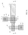
例えば、アモルファス金属ホットエレクトロントランジスタの第1の実施形態は、支持基板102上に形成されたアモルファス金属薄膜トランジスタ構造100の上面図および断面図である図1A~1Cに関して説明される。構造100は、支持基板102上のアモルファス金属相互接続部104と、アモルファス金属相互接続部104上の第1のトンネル絶縁体106とを含む。第1電極108および第2電極110は、第1のトンネル絶縁体106上にある。第1および第2電極108、110は、アモルファス金属相互接続部104と重なる。第3電極112は第2電極110と重なり、第2の絶縁体114によって第2電極から分離されている。 For example, a first embodiment of an amorphous metal hot electron transistor will be described with respect to FIGS. 1A-1C which are top views and cross-sectional views of an amorphous metal thin
この構造は、第1電極108に結合された第1端子121を含む。第2端子122は第2電極110に結合されている。第3端子112(図示せず)は、第3電極112を他の電子デバイスに結合するために含まれてもよい。第1および第2端子121、122は、第3電極と同時に形成することができる。あるいは、第1および第2端子は、第3電極を形成するときの後続の処理ステップで形成される。 This structure includes a
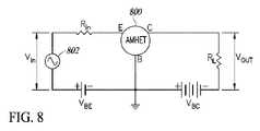
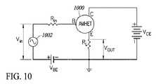
このアモルファス金属薄膜トランジスタ構造100は、第1電極108、第2電極110、および第3電極112に印加される電界を調整することによってトランジスタのように動作する。第1電極108はエミッタ電極とすることができ、第2電極110はベース電極とすることができ、第3電極112はコレクタ電極とすることができる。トランジスタ構造100は、エミッタ接地(common emitter)モード、ベース接地(common base)モード、またはコレクタ接地(common collector)モードで動作することができる。以下の図8、9、および10を参照のこと。 The amorphous metal thin
電子は、第1端子121を通る印加電圧に応答して、第1電極108であるエミッタ電極から第1のトンネル絶縁体106を通ってアモルファス金属相互接続部104へとトンネルする。電子は、アモルファス金属相互接続部104および第1のトンネル絶縁体106を通って第2電極であるベース電極に移動する。これらの電子は、それらのエネルギーが第2電極110、すなわちベース電極のフェルミエネルギーよりも大きいので、トンネリングが終了したときに「ホット」と見なされる。 The electrons tunnel from the emitter electrode, which is the
第2の絶縁体114を横切る電場を調整することによって、より少ないまたはより多くのこれらの「ホット」電子を第3電極112に集めることができ、したがってトランジスタ構造100を通る電流の流れが可能になる。 By adjusting the electric field across the
典型的なトランジスタ構造とは異なり、アモルファス金属トランジスタ構造は、電子が第3電極112から第2電極110およびアモルファス金属相互接続部104を介して第1電極108へ移動するように逆モード(reverse mode)で動作することができる。この逆モードでは、トランジスタ構造100は、調整可能な閾値電圧および非対称性を有するトンネルダイオードのように機能する。調整可能な閾値電圧および非対称性は、第1電極108および第3電極112から印加される電界と組み合わせて第2電極110に印加される電界を変調することによって達成される。 Unlike typical transistor structures, amorphous metal transistor structures are in reverse mode such that electrons move from the
図1Dは、図1A~図1Cのアモルファス金属薄膜トランジスタ構造を形成する方法である。この方法は、ステップ130において、支持基板102の第1の表面128上にアモルファス金属層を形成することを含む。アモルファス金属層は、任意の適切なアモルファス金属によって形成することができる。アモルファス金属の種類の例は、米国特許第8,436,337号、第8,822,978号、第9,099,230号およびPCT出願WO2014/074360号に記載されている。 1D is a method for forming the amorphous metal thin film transistor structure of FIGS. 1A to 1C. This method comprises forming an amorphous metal layer on the
支持基板102は、ガラス基板、プラスチック基板、シリコンまたは他の半導体基板、または可撓性基板などの様々な材料のうちのいずれかとすることができる。支持基板は、非導電性基板とすることができ、これはシリコンまたは半導体基板よりも費用効果が高い。例えば、支持基板は、ホウケイ酸アルミニウムガラス、溶融シリカ、または他の適切な非導電性材料でありうる。基板が導電性である場合、上面と基板上に形成された第1の電子部品との間の基板の上面上に絶縁体を形成することができる。例えば、シリコンまたは半導体基板が使用される場合、非導電性を確実にするために、シリコンから隔離するために、自然酸化物または他の絶縁体が基板の表面に形成される。 The
支持基板102の材料は、トランジスタ構造の最終用途に基づいて製造業者によって選択されうる。例えば、トランジスタ構造がトランジスタ構造のアレイと組み込まれる場合、そのアレイは液晶ディスプレイ内に実装されうる。その他の最終用途にはウェアラブル電子機器がある。支持基板102は、いくつかの反射型ディスプレイに使用できるもののように、透明でも不透明でもよい。 The material of the
非導電性の可撓性支持基板上で製造することにより製造コストを大幅に削減することができる。そのような基板は、トランジスタのロールツーロール製造を可能にすることができる。このような製造変更は、電子サプライチェーンを再定義する可能性がある。 By manufacturing on a non-conductive flexible support substrate, the manufacturing cost can be significantly reduced. Such a substrate can enable roll-to-roll manufacturing of transistors. Such manufacturing changes may redefine the electronic supply chain.
アモルファス金属層を形成した後、この方法は、ステップ132においてアモルファス金属相互接続部104を形成することを含む。これは、アモルファス金属層の余分な部分を除去することを含む。表面128は、その上にアモルファス金属層が形成される平面である。この平坦な表面は、アモルファス金属層の均一で滑らかな表面と関連して、アモルファス金属相互接続部104が均一で滑らかな表面130を有することを可能にし、それにより表面欠陥が少なくなる。これは結晶質金属との比較の上である。結晶性金属の表面の不完全性は電界の不均一性を引き起こし、電子デバイスの故障を招く可能性がある。 After forming the amorphous metal layer, the method comprises forming the
アモルファス金属層の形成は、スパッタリング、溶液堆積、または電子ビーム堆積などの任意の成膜技術を含みうる。例えば、Zr、Cu、Ni、およびAlの元素または混合組成の金属ターゲットを使用したマルチソースRF(またはDC)マグネトロンスパッタリングを使用することができる。スパッタ堆積は、分子線エピタキシー(MBE)または有機金属化学気相堆積(MOCVD)などの高度なエピタキシャル技術を使用して堆積された同様に平滑な半導体よりも明確な製造上の利点をもたらす。 The formation of the amorphous metal layer may include any deposition technique such as sputtering, solution deposition, or electron beam deposition. For example, multi-source RF (or DC) magnetron sputtering using elemental or mixed composition metal targets of Zr, Cu, Ni, and Al can be used. Spatter deposition offers distinct manufacturing advantages over similarly smooth semiconductors deposited using advanced epitaxial techniques such as molecular beam epitaxy (MBE) or organometallic chemical vapor deposition (MOCVD).
上述したように、アモルファス金属層の一部はエッチングされるかあるいは除去される。他の実施形態では、アモルファス金属層はエッチングされず、代わりに用途に適した形状に堆積されてもよい。アモルファス金属層は、スパッタリングによって室温で堆積することができ、その後の加熱工程においてアモルファスおよび滑らかな特性を維持することができる。 As mentioned above, some of the amorphous metal layers are etched or removed. In other embodiments, the amorphous metal layer is not etched and may instead be deposited in a shape suitable for the application. The amorphous metal layer can be deposited at room temperature by sputtering and can maintain amorphous and smooth properties in subsequent heating steps.
ステップ134において、この方法は、アモルファス金属相互接続部104上に第1のトンネル絶縁体106を形成することを含む。第1のトンネル絶縁体は、原子層堆積によって堆積された10ナノメートル以下の酸化アルミニウムなどの非常に薄い層でありうる。非常に薄くなるように形成することができる任意の金属酸化物または窒化物などの他の代替物が利用可能である。第1トンネル絶縁体106は、トンネリングおよびホットエレクトロンの発生を可能にするのに十分に薄い。トンネル絶縁体は、酸化物、窒化物、窒化ケイ素、金属酸化物などを含む任意の適切な絶縁体でありうる。 In
この方法では、第1のトンネル絶縁体106は、ブランケット堆積により共形(conformal)層として形成される。これは最も簡単で最も費用対効果の高い製造オプションであるが、第1のトンネル絶縁体106はトランジスタ構造の最終用途に適するようにパターン化することができる。 In this method, the
ステップ136において、この方法は、第1のトンネル絶縁体106上に第1電極108および第2電極110を形成することを含む。これらはエミッタ電極およびベース電極である。第1および第2電極のそれぞれは、アモルファス金属配線104と重なっている。図1Aの上面図では、第1および第2電極は、アモルファス金属相互接続部に対して横方向または垂直に配置されている。他の向きも可能である。電子の移動を達成するために、電極は何らかの方法でアモルファス金属相互接続部と重なる。 In
第1および第2電極は結晶質金属または他の適切な導体とすることができる。一実施形態では、材料は、ポリシリコン、金属、半導体材料、または高導電性アルミニウム系材料。これらの電極は、グラフェン層のように原子レベルの薄いものでもよい。 The first and second electrodes can be crystalline metal or other suitable conductors. In one embodiment, the material is polysilicon, metal, semiconductor material, or highly conductive aluminum-based material. These electrodes may be thin at the atomic level, such as a graphene layer.
一実施形態では、第1電極108は第2電極と同時に形成される。これは、ブランケット堆積とそれに続くエッチングによるものでありうる。したがって、第1および第2電極は同じ厚さおよび材料特性を有する。代替実施形態では、第1電極108は第2電極とは異なる導電材料である。この実施形態では、第1および第2電極は異なる工程で形成されてもよい。第1および第2電極は、このトランジスタが組み込まれる製品に応じて、異なる厚さ、異なる材料特性、および異なる寸法を有することができる。電子の仕事関数などでエミッタ電極がベース電極とは異なる材料特性を有する場合、その違いのために対称的な伝導は存在しないかもしれない。これは許容できるいくつかの最終用途となる。 In one embodiment, the
ステップ138において、この方法は、第1および第2電極108、110上に第2の絶縁体114を形成することを含む。第2の絶縁体114は、全ての露出面を覆い、理想的には共形である。開口部116、118は、電気的接続が行われる第1および第2電極108、110の表面を露出させる。第2の絶縁体は、酸化物、窒化物、窒化ケイ素、金属酸化物などを含む任意の適切な絶縁体でありうる。 In
ステップ140において、この方法は、第2の絶縁体114上に第3電極112を形成することを含む。第3電極112は、端子121および122をも形成する導電材料から形成されている。この導電材料は、共形的に堆積されエッチングされて、第3電極112および端子121、122を形成する。端子121、122は、第1および第2電極に結合し、他のトランジスタ、LED、または他の電子回路などの他のデバイスへの接続を提供する。 In
後続の工程は、第3電極112上に第3の絶縁体126を形成すること、および第3の絶縁体126の表面を平坦化することを含むことができる。 Subsequent steps can include forming a
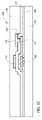
図2A、図2B、および図2Cは、単一のアモルファス金属層206から形成された第1のトランジスタ202および第2のトランジスタ204を含む本開示の代替の実施形態の上面図および断面図である。 2A, 2B, and 2C are top views and cross-sectional views of alternative embodiments of the present disclosure comprising a
アモルファス金属層206は、基板をアモルファス金属層から絶縁するために、非導電性または絶縁体(図示せず)を含む支持基板208上に形成される。トンネル酸化物層210は、アモルファス金属層206上に形成される。第1電極212および第2電極214がトンネル酸化物上に形成され、その上に同一平面上にあり、第1および第2電極の一部はアモルファス金属層206と重なる。 The
誘電体層218が第1および第2電極212、214上に形成されている。誘電体層218上には、第3電極220および第4電極222が形成されている。第3電極および第4電極の一部は、それぞれアモルファス金属層ならびに第1および第2電極と重なり合って整列している。第3および第4電極は同じ材料から同時に形成される。コンタクト224および226もまた、第3および第4電極と同時に形成することができる。接点224は誘電体層を介して第2電極214に結合し、接点226は誘電体層を介して第1電極212に結合する。 The
アモルファス金属層206、第1電極212、および第3電極220の重なりの作る第1の領域228は、電子が第1電極212およびアモルファス金属層206へと、またはこれらから行き来できる場所である。アモルファス金属層206、第2電極214、および第4電極222の重なりに対応する第2の活性領域230がある。この第2の活性領域230は、電子が第2電極214およびアモルファス金属層206へと、またはこれらから行き来できる場所である。 The
第1電極212および第2電極214は、それぞれエミッタおよびベースに対応する。第3および第4電極220、222はコレクタ電極である。これら2つのコレクタ電極は、共有ベース-エミッタ構造を有する2つのトランジスタを形成する。この2トランジスタ構造は、トランジスタ構造100と同じ方法で形成することができ、その違いは、第3電極を形成するときに、より多くの導電層を単に残すことである。 The
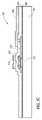
図3A、3B、および3Cは、本開示の別の実施形態によるトランジスタ構造300の上面図および断面図である。トランジスタ構造300は、基板304上に形成されたアモルファス金属膜302を含む。トンネル絶縁体306がアモルファス金属膜302上に位置する。 3A, 3B, and 3C are top views and sectional views of the
1つの領域308において、トンネル絶縁体306は、トンネル絶縁体306の他の領域とは異なる厚さを有するように薄くされるか、あるいはパターン化される。トランジスタ構造300の動作特性は、トンネル絶縁体の厚さを調整することによって調整される。トンネル絶縁体が1つの活性領域において選択的に薄くされている場合、異なる厚さのためにエミッタ-ベース構造を通る対称的な伝導はあり得ない。これは許容できるいくつかの最終用途となる。 In one
第1電極310は、アモルファス金属膜302と重なるように形成され、第1の厚さ312を有するトンネル絶縁体306によってアモルファス金属膜302から分離されている。第2電極314は、第1電極と同じ材料であって同じ処理ステップで形成されてもよく、または異なる時間に形成された異なる材料であってもよく、アモルファス金属膜302と重なるように形成される。第2電極314は、第1電極310から離間しており、第1電極に対してほぼ平行な向きにある。 The
第2電極314は、第1の厚さより薄い第2の厚さ316を有するトンネル絶縁体306によってアモルファス金属膜302から分離されている。厚さが異なる結果、第1電極からアモルファス金属膜302への電子の行き来の挙動は、および第2電極からアモルファス金属膜302へ、および第2電極からアモルファス金属膜302への電子の行き来の挙動とは異なるだろう。例えば、パターン化トンネル絶縁体は、第1および第2電極とアモルファス金属膜との重なり領域に形成されうる寄生容量を最小限に抑えることができる。このように、トンネル絶縁体は、製造および最終製品が要求するように、電極のうちのいずれか1つの重なり領域にパターン形成することができる。The
第1および第2電極310、314上に絶縁体318が形成されている。第3電極320は、第1電極と第2電極の上に形成されている。第3電極320と同時に形成されて、接点322、324がそれぞれ第2電極および第1電極に結合するように形成される。
図3Dは、図3A~図3Cのトランジスタ構造300を製造する例示的なプロセスフローである。ステップ326において、プロセスは基板304上でのアモルファス金属膜の形成を含む。ステップ328において、プロセスは、アモルファス金属膜によりエミッタ-ベース配線を形成することを含む。このエミッタ-ベース配線はアモルファス金属膜302である。この形成は、アモルファス金属膜302の余分な部分をエッチング除去して、アモルファス金属膜302に対して特定の形状を形成することによって達成することができる。 FIG. 3D is an exemplary process flow for manufacturing the
ステップ330において、プロセスは、アモルファス金属膜302上でのエミッタ-ベーストンネル絶縁体の形成を含む。トンネル絶縁体306は、アモルファス金属膜302を完全に覆っている。この実施形態では、トンネル絶縁体306はコンフォーマル層である。他の実施形態では、トンネル絶縁体は、アモルファス金属膜302の上面のみを覆うように、またはアモルファス金属膜302の上面の一部分に関連する領域のみを覆うように、異なる方法で形成することができる。第1および第2電極の重なり合い。 In
ステップ332において、プロセスは、エミッタ-ベーストンネル絶縁体を選択的にエッチングして、第2電極、すなわちベース電極に関連する第2の厚さ316を形成することを含む。ステップ334において、プロセスはベースおよびエミッタ電極、すなわち第1および第2電極を形成することを含む。これは、第1および第2電極の形状を形成するための堆積およびエッチングによって達成することができる。 In
ステップ336において、プロセスは、第1および第2電極上にコレクタ-ベース絶縁体を形成することを含む。第1および第2電極へのアクセスを提供するために、開口340などの開口がコレクタ-ベース絶縁体(絶縁体318)に形成される。 In
ステップ338において、プロセスは、コレクタ電極と、第3電極320および接点322などの他の接点とを形成することを含む。 In
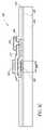
図4A、4B、および4Cは、異なる寸法のベース電極およびエミッタ電極を有するトランジスタ構造400に関する本開示の代替の実施形態である。トランジスタ構造は平面基板404上にアモルファス金属相互接続部402を含む。アモルファス金属相互接続部402は、上から見た斜視図から長方形であり、断面線4B-4Bに沿って第1の方向に延びる最長寸法を有する。 4A, 4B, and 4C are alternative embodiments of the present disclosure for a
トンネル絶縁体406が相互接続部402上にある。エミッタ電極408がトンネル絶縁体406上にある。ベース電極410も、エミッタ電極から間隔を置いてトンネル絶縁体406上にある。エミッタ電極とベース電極の両方は、少なくとも部分的に相互接続部402の上にあり、相互接続部402と重なる。 The
ベース電極は、エミッタ電極408の第2の寸法416よりも小さい第1の寸法414を有する相互接続部402の上にあってそれと整列している部分412を少なくとも含む。寸法が異なるとトランジスタの動作特性が変わり、製造業者はトランジスタ構造を調整することができる。例えば、トランジスタ構造の利得は、ベース電極をより薄くすることによって増加させることができる。ベース電極とエミッタ電極とは、同じ材料でもよく異なる材料でもよい。 The base electrode comprises at least a
ベース電極は、ベース電極の第1の部分が第1の厚さであり、ベース電極の第2の部分が第1の厚さよりも小さい第2の厚さであるように、第1の厚さを有するように形成され、次いで薄くされうる。あるいは、ベース電極は、エミッタ電極とは異なる処理ステップで形成され、エミッタ電極よりも薄く形成されてもよい。一旦形成されたベース電極の一部を除去する代わりに、ベース電極をエミッタ電極よりも薄い層として形成することができる。 The base electrode has a first thickness so that the first portion of the base electrode has a first thickness and the second portion of the base electrode has a second thickness smaller than the first thickness. Can be formed to have and then thinned. Alternatively, the base electrode may be formed in a different processing step from the emitter electrode and may be formed thinner than the emitter electrode. Instead of removing a part of the base electrode once formed, the base electrode can be formed as a layer thinner than the emitter electrode.
第1の誘電体層418がベース電極およびエミッタ電極上に形成されている。第1の誘電体層418上にコレクタ電極420が形成されている。ベース電極へのコンタクト422は、コレクタ電極と同時にかつ同じ材料から形成することができる。第1の誘電体層を貫通する開口部は、ベース電極への接触を可能にするように形成される。別の接点424を同様にエミッタ電極に形成することができる。 The
第2の誘電体層426がコレクタ電極および接点422、424上に形成されてもよい。いくつかの実施形態では、コレクタ端子を他のデバイスに結合するために、コンタクト428が第2の誘電体層426を貫通して形成される。 A
図5A、5B、および5Cは、本開示の別の実施形態に従って形成されたトランジスタ構造500の上面図および断面図である。このトランジスタ構造500は、基板504上に形成されたアモルファス金属層502を含む。アモルファス金属層502上にトンネル酸化膜506を形成する。トンネル酸化物層506上にバリア層508が形成される。バリア層508は、金属酸化物などの無機材料、またはポリマーなどの有機材料、または任意の適切な材料とすることができる。バリア層508は、アモルファス金属と電極の重なりのために生じうる寄生容量を最小限に抑えることができる。 5A, 5B, and 5C are top views and cross-sectional views of the
第1の開口部510はバリア層508に形成されている。第1開口部510には第1電極512が形成されている。第1電極はアモルファス金属層502と重なる。アモルファス金属層502の一部と重なる第2の開口部507がバリア層508に形成されている。第2電極514がアモルファス金属層502と重なるように形成され、第2電極の一部は第2の開口部507内にある。 The
誘電体層516は第1および第2電極512、514上に形成されている。誘電体層上に第3電極518が形成される。この実施形態および本開示に記載されている他の実施形態ではいずれの層も平坦化されていない。他の実施形態では、最終製品が必要とする場合のために、各層または各層を平坦化することができる。 The dielectric layer 516 is formed on the first and
第4電極520および第5電極522は、それぞれ第1電極512および第2電極514に結合する。第4および第5電極520、522は、第3電極518と同じ材料から同時に形成することができる。 The
本実施形態または本開示の任意の実施形態における第1および第2電極は、グラフェン、MoS2、W2、Ti3C2、GaN、BN、Ca2N、または他の適切な材料などの超薄型の2次元導体で形成されうる。トランジスタ構造の利得を調整するために異なる材料を選択することができる。いくつかの実施形態では、第1電極が導電性材料の原子的に薄い層であり、第2電極は導電性材料のかなり厚い層である。これらの層のための導電材料は異なる種類の導体でありうる。The first and second electrodes in this embodiment or any embodiment of the present disclosure are super such as graphene, MoS2 , W2 , Ti3 C2 , GaN, BN, Ca2 N, or other suitable materials. It can be formed of a thin two-dimensional conductor. Different materials can be selected to adjust the gain of the transistor structure. In some embodiments, the first electrode is an atomically thin layer of conductive material and the second electrode is a fairly thick layer of conductive material. The conductive material for these layers can be different types of conductors.
図6は、基板606の凹部604内に形成されたアモルファス金属層602を有するトランジスタ構造600を含む本開示の代替の実施形態である。アモルファス金属層602の第1の面608は、基板606の第1の面610と同一平面上にある。 FIG. 6 is an alternative embodiment of the present disclosure comprising a
トンネル酸化物層612が、アモルファス金属層602および基板の第1の表面上に形成される。トンネル酸化膜612上に第1および第2電極614、616を形成する。第1電極614はアモルファス金属層の第1の部分と重なり合い、第2電極616はアモルファス金属層の第2の部分と重なり合う。 The
第1の誘電体層618が第1および第2電極上にある。第3電極620は、第1の誘電体層618の平面上に形成されている。第2の誘電体層622が第3電極上にある。 A
図7は、基板704の平面上にアモルファス金属層702を有するトランジスタ構造700を有する本開示の代替の実施形態である。トンネル酸化物層706がアモルファス金属層702上にある。アモルファス金属層702の側面708とトンネル酸化物層706の側面710は同一平面上にある。これは、アモルファス層を形成し、酸化物層をトンネルし、次に両方の層を同時にエッチングすることによって形成することができる。 FIG. 7 is an alternative embodiment of the present disclosure having a
第1および第2電極712、714がトンネル酸化物層上に形成される。誘電体層716が第1および第2電極上に形成されている。誘電体層716上に第3電極718が形成されている。 The first and
図8は、本開示のトランジスタ構造に従って形成されたベース接地トランジスタ構造である。アモルファスホットエレクトロントランジスタ800は、エミッタE、ベースB、およびコレクタCを有する。ベースはグランドに結合されている。コレクタは、負荷を表し他の回路でありうる抵抗RLに結合されている。電源VBCはグランドと抵抗RLとの間に結合されている。電源VBEはグランドと抵抗Rinとの間に結合されている。電流源802が電圧源VBEと抵抗Rinとの間に結合されている。抵抗RinはエミッタEに結合されている。FIG. 8 is a base grounded transistor structure formed according to the transistor structure of the present disclosure. The amorphous
図9は、本開示のトランジスタ構造に従って形成されたエミッタ接地トランジスタ900である。トランジスタ900は、エミッタE、ベースB、およびコレクタCを有するアモルファスホットエレクトロントランジスタである。エミッタはグランドに結合されている。コレクタは、負荷を表し他の回路でありうる抵抗RLに結合されている。電圧源VCEはグランドと抵抗RLとの間に結合されている。電圧源VBEはグランドと抵抗Rinとの間に結合されている。電流源902は電圧源VBEと抵抗Rinとの間に結合されている。抵抗RinはベースBに結合されている。FIG. 9 is a grounded
図10は、本開示のトランジスタ構造に従って形成されたコレクタ接地トランジスタ1000である。トランジスタ1000は、エミッタE、ベースB、およびコレクタCを有するアモルファスホットエレクトロントランジスタである。エミッタEは、負荷を表し他の回路でありうる抵抗RLを介してグランドに結合されている。電圧源VCEはグランドとコレクタCとの間に結合されている。電圧源VBEはグランドと抵抗Rinとの間に結合されている。電流源1002は電圧源VBEと抵抗Rinの間に結合される。抵抗RinはベースBに結合されている。FIG. 10 is a collector grounded
図11Aおよび図11Bは、単一段エミッタ接地増幅回路および関連する信号表現である。これは、増幅器などの一般的な回路にAMHETを組み込んだ表示である。図11Bでは、DCバイアス電圧Qが示されている。このバイアス電圧Qは、第1の抵抗R1、第2の抵抗R2、および第1のキャパシタC1が互いに結合されてAMHET1100に結合される接合部に印加される。グランドと第1のキャパシタCiのプレートとの間に印加される電圧入力Vinがある。電圧VCCが第1の抵抗Riおよび負荷抵抗RLに結合されている。第2のキャパシタC2は第3の抵抗REとグランドとの間に結合されている。出力信号VOUTは、図11Bに示す増幅信号である。11A and 11B are single-stage grounded-emitter amplifier circuits and related signal representations. This is a display in which AMHET is incorporated in a general circuit such as an amplifier. In FIG. 11B, the DC bias voltage Q is shown. This bias voltage Q is applied to the junction where the first resistance R1 , the second resistance R2 , and the first capacitor C1 are coupled to each other and coupled to the
図12および図13は、本開示の複数のトランジスタを組み込んだ回路図である。図12は、フリップフロップ配置にある、第1のAMHET(アモルファス金属ホットエレクトロントランジスタ)1200および第2のAMHET1202を含む。第1および第2のAMHETのエミッタEのそれぞれはグランドに結合されている。各ベースBは、第1の抵抗1204、1206に結合されている。第1の抵抗の各々もまた電圧源VBBに結合されている。第1のAMHET1200のベースBは第2の抵抗1208に結合されている。第2の抵抗1208は第3の抵抗1210を介して第2のAMHET1202のコレクタCに結合されている。第2のAMHET1202のベースBは第1のAMHET1200のコレクタCに結合されている。第4の抵抗1212は、第1のAMHETのコレクタCと電圧源VCCとの間に結合される。第5の抵抗1214は、第2のAMHETのコレクタと電圧源VCCとの間に結合される。12 and 13 are circuit diagrams incorporating the plurality of transistors of the present disclosure. FIG. 12 includes a first AMHET (amorphous metal hot electron transistor) 1200 and a
このAMHETフリップフロップ構造は、カウンタ、シフトレジスタ、クロックパルス発生器、または他の回路などの様々なスイッチング用途に統合することができる。これらは、メモリ回路、リレー制御機能、またはレーダー用途または通信システムなどのような他の機能に統合することができる。最終用途にむけ信号を整形するためにキャパシタ部品を含めることができる。 This AMHET flip-flop structure can be integrated into various switching applications such as counters, shift registers, clock pulse generators, or other circuits. These can be integrated into memory circuits, relay control functions, or other functions such as radar applications or communication systems. Capacitor components can be included to shape the signal for end use.
図13は、第1のAMHET1300および第2のAMHET1302を含む回路構造の代替実施形態である。第1のAMHETのエミッタEは第2のAMHETのベースBに結合されている。1番目と2番目のAMHETのコレクタは結合されている。第1のAMHET1300のベースは、負荷または他の回路を表す抵抗RBに結合されている。コレクタCは、負荷または他の回路を表す抵抗RLに結合されている。抵抗RLは電圧VCCに結合されている。第2のAMHET1302のエミッタEはグランドに結合されている。FIG. 13 is an alternative embodiment of a circuit structure comprising a
図14は、アレイ状の本開示のトランジスタ構造である。アレイはディスプレイに組み込むことができ、またはX線検出器内などのセンサと一体化することができる。アレイ1400は、複数の行1404と複数の列1402を含む。各行は、アレイのAMHETトランジスタ1401にベース信号を伝達することができる。各列はエミッタ信号をAMHETトランジスタ1401に伝えることができる。AMHETトランジスタ1401は、アモルファス金属層1406を含む。エミッタ電極1410は、アモルファス金属層1406と重なり合い、行1402に結合する。ベース電極1408は、アモルファス金属層1406と重なり合い、そして柱1404に結合する。コレクタ電極およびコンタクト1414は、アモルファス金属層1406およびベース電極1408と重なる。コレクタ電極1414は他の画素またはセル制御素子に結合されている。コレクタ電極1414は、キャパシタまたは他のトランジスタに結合することができる。FIG. 14 is an array-shaped transistor structure of the present disclosure. The array can be integrated into the display or integrated with a sensor, such as in an X-ray detector. The
このAMHETトランジスタ1401は、ベース接地、エミッタ接地、またはコレクタ接地モードのマトリクススイッチとして動作することができる。この特定の図は、一般的なエミッタ構成である。そのようなマトリックススイッチは、単一の要素が制御されることを可能にする。 The
複数のAMHETトランジスタ1401は、液晶ディスプレイ、有機発光ダイオードディスプレイ、電気泳動、エレクトロルミネセンスなどのような様々なアクティブマトリックスディスプレイ技術に組み込むことができる。それぞれの特定のアクティブマトリックス用途は、ディスプレイを形成するための追加の回路要素を有するであろう。抵抗、キャパシタ、ダイオード、他のトランジスタ、または他の電子部品などのいくつかの要素は、AMHETと同じ処理ステップまたは後続の処理で形成することができる。図15は、AMHET1502を含む液晶表示回路1500の一例である。AMHET1502のエミッタEは、蓄積キャパシタ1504および液晶キャパシタ1506に結合されている。蓄積キャパシタ1504および液晶キャパシタ1506のそれぞれもまたグランドに結合されている。AMHET1502のベースは抵抗RBに結合されている。AMHET1502のコレクタは抵抗RLに結合されている。The plurality of
図16は、第1のAMHET1604および第2のAMHET1606を含む有機発光ダイオード(OLED)1602を駆動するための回路1600である。第1のAMHETのエミッタEは第2のAMHETのベースに結合されている。第2のAMEHTのベースとグランドとの間に蓄積キャパシタが結合されている。第2のAMEHTのエミッタはOLEDに結合されている。 FIG. 16 is a
上記の様々な実施形態は、さらなる実施形態を提供するために組み合わせることができる。2016年7月7日に出願された米国仮特許出願第62/359,596号は、その全体を引用することにより本明細書の一部を成すものとする。 The various embodiments described above can be combined to provide further embodiments. U.S. Provisional Patent Application No. 62 / 359,596, filed July 7, 2016, is incorporated herein by reference in its entirety.
上記の詳細な説明に照らして、これらおよび他の変更を実施形態に加えることができる。一般に、添付の特許請求の範囲において、使用される用語は、特許請求の範囲を明細書および特許請求の範囲に開示された特定の実施形態に限定するように解釈されるべきではなく、実施形態と、そのような特許請求の範囲に対し権利が認められるべき等価物の全範囲とを含むものと解されるべきである。したがって、特許請求の範囲は本開示による限定をうけるものではない。 These and other modifications can be made to the embodiments in the light of the above detailed description. In general, the terms used in the appended claims should not be construed to limit the scope of the claims to the specific embodiments disclosed in the specification and claims, and embodiments. And should be construed to include the full range of equivalents to which the rights should be granted for such claims. Therefore, the scope of claims is not limited by this disclosure.
Claims (21)
Translated fromJapanese前記非導電性基板上のアモルファス金属層と、
前記アモルファス金属層上の第1の誘電体層と、
それぞれが前記アモルファス金属層と重なっている、前記第1の誘電体層上の第1電極および第2電極と、
前記第1電極および前記第2電極上の第2の誘電体層と、
前記第2電極および前記アモルファス金属層に重なっている、前記第2の誘電体層上の第3電極と
を備えるデバイス。With a non-conductive substrate
The amorphous metal layer on the non-conductive substrate and
The first dielectric layer on the amorphous metal layer and
The first and second electrodes on thefirst dielectric layer, each of which overlaps the amorphous metal layer,
With the first electrode and the second dielectric layer onthe second electrode,
With the second electrode and the third electrode on the second dielectric layer overlappingthe amorphous metal layer
A device equipped with .
請求項1に記載のデバイス。The first and second electrodes are crystalline metals onthe first dielectric layer.
The device according to claim 1.
請求項1に記載のデバイス。The first electrode is a first conductive material, and the second electrode is a second conductive material different from the first conductive material.
The device according to claim 1.
請求項1に記載のデバイス。The first electrode and the second electrode are the same conductive material.
The device according to claim 1.
請求項1に記載のデバイス。The first dielectric layer comprises a metal oxide or a metal nitride.
The device according to claim 1.
請求項1に記載のデバイス。The first electrode has a first thickness, and the second electrode has a second thickness different from the first thickness.
The device according to claim 1.
請求項1に記載のデバイス。The first dielectriclayer comprises a recess and the second electrode is in the recess.
The device according to claim 1.
請求項7に記載のデバイス。The recesses overlap and align with the amorphous metal layer.
The device according to claim 7.
請求項1に記載のデバイス。The amorphous metal layerextends lengthwise along the first direction, and the first and second electrodesextend lengthwise along a second direction across the first direction.
The device according to claim 1.
請求項1に記載のデバイス。The device according to claim 1, further comprising a first terminal coupled to the first electrode and a second terminal coupled to the second electrode.
請求項10に記載のデバイス。The first terminal is coupled to the first electrode viathe second dielectric layer, and the second terminal is coupled to the second electrode viathe second dielectric layer.
The device according to claim 10.
前記基板上のアモルファス金属層であって、第1の方向に沿って延びる長さと、第1の方向を横切る第2の方向に沿って延びる幅とを有するアモルファス金属層と、
前記アモルファス金属層上の第1の絶縁体層と、
前記第1の絶縁体層上のエミッタ電極であって、アモルファス金属層の第1の部分と重なるエミッタ電極は、前記第2の方向に沿って延びる長さと、前記第1の方向に沿って延びる幅とを有しているエミッタ電極と、
前記第1の絶縁体層上のベース電極であって、前記アモルファス金属層の第2の部分と重なり、前記第2の方向に沿って延びる長さと、前記第1の方向に沿って延びる幅とを有している、ベース電極と、
前記エミッタ電極および前記ベース電極上の第2の絶縁体層と、
前記第2の絶縁体層上のコレクタ電極であって、前記ベース電極および前記アモルファス金属層の前記第2の部分に重なる前記コレクタ電極と
を備えるデバイス。With the board
An amorphous metal layer on the substrate having a length extending along a first direction and a width extending along a second direction across the first direction.
The first insulator layer on the amorphous metal layer and
The emitter electrode onthe first insulator layer , which overlaps with the first portion of the amorphous metal layer, has a length extending along the second direction and extending along the first direction. With an emitter electrode having a width and
A base electrode onthe first insulator layer that overlaps with a second portion of the amorphous metal layer and has a length extending along the second direction and a width extending along the first direction. Has a base electrode and
A second insulatorlayer on the emitter electrode and the base electrode,
A device comprising a collector electrode onthe second insulatorlayer , the base electrode and the collector electrode overlapping the second portion of the amorphous metal layer.
請求項12に記載のデバイス。The collector electrode has a length extending along the first direction and a width extending along the second direction, and the width is smaller than the length.
The device according to claim 12.
請求項12に記載のデバイス。The length of the emitter electrode is larger than the width of the emitter electrode, and the length of the base electrode is larger than the width of the base electrode.
The device according to claim 12.
前記アモルファス金属層の上方に第1の共形誘電体層を形成するステップと、
前記第1の共形誘電体層上に第1の導電層を形成するステップと、
前記第1の導電層をパターニングしてエミッタ端子とベース端子を形成するステップと、
前記エミッタ端子と前記ベース端子の上方に第2の共形誘電体層を形成するステップと、
前記第2の共形誘電体層に開口部をパターニングするステップと、
前記開口部を第2の導電層で充填することによって前記エミッタ端子および前記ベース端子への接点を形成するステップと、
前記第2の導電層をパターニングして集電端子を形成するステップと
を含む方法。Steps to form an amorphous metal layer on a non-conductive substrate,
A step of forming a first conformal dielectric layer above the amorphous metal layer,
The step of forming the first conductive layer on the first conformal dielectric layer,
The step of patterningthe first conductive layer to form an emitter terminal and a base terminal,
A step of forming a second conformal dielectric layer above the emitter terminal and the base terminal,
The step of patterning the opening in the second conformal dielectric layer,
A step of forming contacts to the emitter terminal and the base terminal by filling the opening with a second conductive layer.
A method including the step of patterningthe second conductive layer to form a current collecting terminal.
請求項15に記載の方法。The step of forming the second conformal dielectric layer includes the step of forming the secondconformal dielectric layer having athickness larger than that of the first conformal dielectric layer.
The method according to claim 15.
前記基板上のアモルファス金属層と、
前記アモルファス金属層上の第1の絶縁体と、
前記第1の絶縁体上にあり、前記アモルファス金属層の第1の部分と重なる第1電極と、
前記第1の絶縁体上にあり、前記アモルファス金属層の第2の部分と重なる第2電極と、
第2の絶縁体と、
前記第2の絶縁体を貫通し、前記第1電極に結合された第1の接点と、
前記第2の絶縁体を貫通し、前記第2電極に結合された第2の接点と、
前記第2の絶縁体上にあり、前記アモルファス金属層の前記第2の部分と重なる第3電極と
を備えるデバイス。With the board
The amorphous metal layer on the substrate and
With the first insulator on the amorphous metal layer,
A first electrode on the first insulator and overlapping with the first portion of the amorphous metal layer.
A second electrode on the first insulator and overlapping the second portion of the amorphous metal layer.
With the second insulator,
With the first contact penetrating the second insulator and coupled to the first electrode,
A second contact that penetrates the second insulator and is coupled to the second electrode.
A device that is on the second insulator and includes a third electrode that overlaps the second portion of the amorphous metal layer.
請求項17に記載のデバイス。17. The device of claim 17, further comprising a fourth electrode that is on the second insulator and overlaps the first portion of the amorphous metal layer.
請求項17に記載のデバイス。The first electrode is thicker than the second electrode,
17. The device of claim 17.
請求項17に記載のデバイス。17. The device of claim 17, further comprising a thirdinsulator between the firstinsulator and the first and second electrodes.
前記アモルファス金属層の前記第2の部分における前記第3の絶縁体の第2の開口部と
をさらに備える請求項20に記載のデバイス。With the first opening of the thirdinsulator in the first portion of the amorphous metal layer,
20. The device of claim 20, further comprising a second opening of the thirdinsulator in the second portion of the amorphous metal layer.
Applications Claiming Priority (3)
| Application Number | Priority Date | Filing Date | Title |
|---|---|---|---|
| US201662359596P | 2016-07-07 | 2016-07-07 | |
| US62/359,596 | 2016-07-07 | ||
| PCT/US2017/041252WO2018009901A1 (en) | 2016-07-07 | 2017-07-07 | Amorphous metal hot electron transistor |
Publications (2)
| Publication Number | Publication Date |
|---|---|
| JP2019525461A JP2019525461A (en) | 2019-09-05 |
| JP7068265B2true JP7068265B2 (en) | 2022-05-16 |
Family
ID=60901738
Family Applications (1)
| Application Number | Title | Priority Date | Filing Date |
|---|---|---|---|
| JP2019500256AActiveJP7068265B2 (en) | 2016-07-07 | 2017-07-07 | Amorphous metal hot electron transistor |
Country Status (6)
| Country | Link |
|---|---|
| US (2) | US10672898B2 (en) |
| JP (1) | JP7068265B2 (en) |
| KR (1) | KR102443767B1 (en) |
| CN (1) | CN109564892B (en) |
| TW (1) | TWI678738B (en) |
| WO (1) | WO2018009901A1 (en) |
Families Citing this family (9)
| Publication number | Priority date | Publication date | Assignee | Title |
|---|---|---|---|---|
| JP6692439B2 (en) | 2015-10-13 | 2020-05-13 | アモルフィックス・インコーポレイテッド | Amorphous metal thin film Non-linear resistance |
| JP7068265B2 (en) | 2016-07-07 | 2022-05-16 | アモルフィックス・インコーポレイテッド | Amorphous metal hot electron transistor |
| JP2021520060A (en)* | 2018-03-30 | 2021-08-12 | アモルフィックス・インコーポレイテッド | Amorphous metal thin film transistor |
| US11830961B2 (en)* | 2018-09-02 | 2023-11-28 | Newport Fab, Llc | Silicon nitride hard mask for epitaxial germanium on silicon |
| CN110137192A (en)* | 2019-04-19 | 2019-08-16 | 华中科技大学 | A kind of molybdenum sulfide image sensing memory and its preparation method |
| CN110808266A (en)* | 2019-10-15 | 2020-02-18 | 深圳市华星光电技术有限公司 | Display substrate with transparent electrode and preparation method thereof |
| KR20230041683A (en) | 2020-06-12 | 2023-03-24 | 아모르픽스, 인크 | Circuits for electronic devices with non-linear components |
| DE102020116068A1 (en) | 2020-06-18 | 2021-12-23 | Westfälische Wilhelms-Universität Münster | Transparent resonant tunnel diode and process for its manufacture |
| CN116421166A (en)* | 2023-04-25 | 2023-07-14 | 北京理工大学 | An intelligent micro-robot and processing method for sensing signals in the human body |
Citations (3)
| Publication number | Priority date | Publication date | Assignee | Title |
|---|---|---|---|---|
| JP2007535178A (en) | 2004-04-26 | 2007-11-29 | ザ リージェンツ オブ ザ ユニヴァーシティー オブ コロラド | Hot electron transistor |
| US20100289005A1 (en) | 2009-05-12 | 2010-11-18 | The State Of Oregon Acting By And Through The State Board Of Higher Education On Behalf Of | Amorphous multi-component metallic thin films for electronic devices |
| JP2016502268A (en) | 2012-11-12 | 2016-01-21 | オレゴン ステイト ユニバーシティ | Amorphous metal thin film nonlinear resistor |
Family Cites Families (44)
| Publication number | Priority date | Publication date | Assignee | Title |
|---|---|---|---|---|
| US4204275A (en)* | 1978-10-20 | 1980-05-20 | Harris Corporation | Unisolated EAROM memory array |
| JPH02137828A (en) | 1988-11-18 | 1990-05-28 | Seiko Instr Inc | Input protection device for electrooptical device |
| JPH0750697B2 (en) | 1989-02-20 | 1995-05-31 | 株式会社東芝 | Method for manufacturing semiconductor device |
| EP0434627A3 (en) | 1989-12-18 | 1991-10-23 | Ois Optical Imaging Systems, Inc. | Balanced drive symmetric mim diode configuration for liquid crystal displays and method of operating same |
| US5212537A (en) | 1990-07-12 | 1993-05-18 | Applied Materials, Inc. | Calibration technique for monochromators and spectrophotometers |
| JPH0476954A (en)* | 1990-07-19 | 1992-03-11 | Ricoh Co Ltd | MIMIM element |
| JPH05102147A (en) | 1991-10-07 | 1993-04-23 | Sony Corp | Method for forming amorphous metal and semiconductor device with amorphous metal film |
| US6714625B1 (en)* | 1992-04-08 | 2004-03-30 | Elm Technology Corporation | Lithography device for semiconductor circuit pattern generation |
| US5893621A (en) | 1994-07-14 | 1999-04-13 | Citizen Watch Co., Ltd. | Liquid crystal display and method of manufacturing the same |
| GB9525784D0 (en)* | 1995-12-16 | 1996-02-14 | Philips Electronics Nv | Hot carrier transistors and their manufacture |
| JP3193973B2 (en) | 1997-07-03 | 2001-07-30 | 松下電器産業株式会社 | Capacitive element and method of manufacturing the same |
| JPH11305267A (en) | 1998-04-23 | 1999-11-05 | Seiko Epson Corp | Active matrix substrate, method of manufacturing the same, liquid crystal panel and electronic equipment using the same |
| JP4019600B2 (en) | 1998-11-30 | 2007-12-12 | セイコーエプソン株式会社 | Electro-optical device and projector |
| WO2000033285A1 (en) | 1998-11-30 | 2000-06-08 | Seiko Epson Corporation | Electro-optical device and its manufacturing method |
| TW500937B (en) | 1999-07-13 | 2002-09-01 | Samsung Electronics Co Ltd | Liquid crystal display |
| US7173275B2 (en)* | 2001-05-21 | 2007-02-06 | Regents Of The University Of Colorado | Thin-film transistors based on tunneling structures and applications |
| JP4157707B2 (en) | 2002-01-16 | 2008-10-01 | 株式会社東芝 | Magnetic memory |
| JP2003347308A (en)* | 2002-05-22 | 2003-12-05 | Nec Compound Semiconductor Devices Ltd | Semiconductor device and manufacturing method thereof |
| US7330369B2 (en)* | 2004-04-06 | 2008-02-12 | Bao Tran | NANO-electronic memory array |
| CN101577231B (en) | 2005-11-15 | 2013-01-02 | 株式会社半导体能源研究所 | Semiconductor device and method of manufacturing the same |
| JP2008004588A (en) | 2006-06-20 | 2008-01-10 | Epson Imaging Devices Corp | Nonlinear element manufacturing method, nonlinear element, and electro-optical device |
| CN100576472C (en)* | 2006-12-12 | 2009-12-30 | 中芯国际集成电路制造(上海)有限公司 | Semiconductor device with amorphous silicon MONOS memory cell structure and manufacturing method thereof |
| JP4545780B2 (en) | 2007-07-09 | 2010-09-15 | 株式会社 日立ディスプレイズ | Manufacturing method of organic light emitting display device |
| JP2009130167A (en) | 2007-11-26 | 2009-06-11 | Renesas Technology Corp | Semiconductor device and manufacturing method thereof |
| US9306078B2 (en)* | 2008-09-08 | 2016-04-05 | Cbrite Inc. | Stable amorphous metal oxide semiconductor |
| JP2010123338A (en) | 2008-11-18 | 2010-06-03 | Canon Inc | Image display apparatus |
| US8838116B2 (en) | 2009-05-19 | 2014-09-16 | Qualcomm Incorporated | Minimizing interference to non-associated users |
| US8575753B2 (en) | 2009-05-27 | 2013-11-05 | Samsung Electronics Co., Ltd. | Semiconductor device having a conductive structure including oxide and non oxide portions |
| KR20170091760A (en) | 2009-11-27 | 2017-08-09 | 가부시키가이샤 한도오따이 에네루기 켄큐쇼 | Semiconductor device |
| US8530273B2 (en) | 2010-09-29 | 2013-09-10 | Guardian Industries Corp. | Method of making oxide thin film transistor array |
| WO2012129176A1 (en) | 2011-03-18 | 2012-09-27 | The State Of Oregon Acting By And Through The State Board Of Higher Education On Behalf Of Oregon State University | Amorphous multi-component metal/metal oxide nanolaminate metamaterials and devices based thereon |
| US9006024B2 (en) | 2012-04-25 | 2015-04-14 | Semiconductor Energy Laboratory Co., Ltd. | Method for manufacturing semiconductor device |
| CN103594521B (en)* | 2012-08-17 | 2017-03-01 | 瀚宇彩晶股份有限公司 | semiconductor element |
| CN104022044B (en) | 2013-03-01 | 2017-05-10 | 北京京东方光电科技有限公司 | Oxide thin-film transistor and preparation method thereof, array substrate and display device |
| CN103268891B (en) | 2013-03-28 | 2016-08-10 | 北京京东方光电科技有限公司 | A kind of thin film transistor (TFT), amorphous silicon flat panel detection substrate and preparation method |
| US9564478B2 (en) | 2013-08-26 | 2017-02-07 | Apple Inc. | Liquid crystal displays with oxide-based thin-film transistors |
| US9876183B2 (en) | 2015-01-30 | 2018-01-23 | Northwestern University | Charge-transporting metal oxide-polymer blend thin films |
| KR102535073B1 (en) | 2015-07-24 | 2023-05-19 | 오레곤 스테이트 유니버시티 | In-Plane Switching Liquid Crystal Display Backplane Using Amorphous Metal Nonlinear Resistors as Active Sub-Pixel Devices |
| CN204994473U (en) | 2015-08-03 | 2016-01-27 | 上海爱农机电设备有限公司 | Portable superfine atomizing machine |
| JP6692439B2 (en) | 2015-10-13 | 2020-05-13 | アモルフィックス・インコーポレイテッド | Amorphous metal thin film Non-linear resistance |
| KR20170087574A (en) | 2016-01-20 | 2017-07-31 | 삼성디스플레이 주식회사 | Liquid crystal display device and manufacturing method thereof |
| JP7068265B2 (en) | 2016-07-07 | 2022-05-16 | アモルフィックス・インコーポレイテッド | Amorphous metal hot electron transistor |
| KR102071145B1 (en) | 2017-09-18 | 2020-01-29 | 고려대학교 세종산학협력단 | Stretchable multimodal sensor and method of fabricating of the same |
| KR101934026B1 (en) | 2017-09-21 | 2018-12-31 | 고려대학교 세종산학협력단 | Electrode or wiring comprising amorphous metal layer, flexible display device comprising the same and manufacturing method thereof |
- 2017
- 2017-07-07JPJP2019500256Apatent/JP7068265B2/enactiveActive
- 2017-07-07KRKR1020197002221Apatent/KR102443767B1/enactiveActive
- 2017-07-07USUS16/309,804patent/US10672898B2/enactiveActive
- 2017-07-07TWTW106122857Apatent/TWI678738B/enactive
- 2017-07-07WOPCT/US2017/041252patent/WO2018009901A1/ennot_activeCeased
- 2017-07-07CNCN201780042032.XApatent/CN109564892B/enactiveActive
- 2020
- 2020-04-28USUS16/861,098patent/US11069799B2/enactiveActive
Patent Citations (3)
| Publication number | Priority date | Publication date | Assignee | Title |
|---|---|---|---|---|
| JP2007535178A (en) | 2004-04-26 | 2007-11-29 | ザ リージェンツ オブ ザ ユニヴァーシティー オブ コロラド | Hot electron transistor |
| US20100289005A1 (en) | 2009-05-12 | 2010-11-18 | The State Of Oregon Acting By And Through The State Board Of Higher Education On Behalf Of | Amorphous multi-component metallic thin films for electronic devices |
| JP2016502268A (en) | 2012-11-12 | 2016-01-21 | オレゴン ステイト ユニバーシティ | Amorphous metal thin film nonlinear resistor |
Also Published As
| Publication number | Publication date |
|---|---|
| KR102443767B1 (en) | 2022-09-15 |
| CN109564892B (en) | 2023-05-12 |
| KR20190018008A (en) | 2019-02-20 |
| US20200259008A1 (en) | 2020-08-13 |
| TWI678738B (en) | 2019-12-01 |
| CN109564892A (en) | 2019-04-02 |
| US10672898B2 (en) | 2020-06-02 |
| TW201806034A (en) | 2018-02-16 |
| US20190318926A1 (en) | 2019-10-17 |
| WO2018009901A1 (en) | 2018-01-11 |
| JP2019525461A (en) | 2019-09-05 |
| US11069799B2 (en) | 2021-07-20 |
Similar Documents
| Publication | Publication Date | Title |
|---|---|---|
| JP7068265B2 (en) | Amorphous metal hot electron transistor | |
| US9362413B2 (en) | MOTFT with un-patterned etch-stop | |
| US12336205B2 (en) | Amorphous metal thin film transistors | |
| KR100388272B1 (en) | A triodic rectifier switch device | |
| CN102543723A (en) | Method for manufacturing grid controlled diode semiconductor device | |
| KR20200029674A (en) | Thin film transistor, manufacturing method thereof and diode including the same | |
| US12075656B2 (en) | Circuits including non-linear components for electronic devices | |
| JPS58170065A (en) | Method for manufacturing thin film field effect transistors | |
| KR20140078190A (en) | Transistor and method of manufacturing the same | |
| CN113035954B (en) | Full-surrounding gate horizontal penetration type transistor and preparation method thereof | |
| CN120500088A (en) | Laminated channel hybrid contact thin film transistor and preparation method thereof | |
| CN118280998A (en) | Display device and manufacturing method thereof | |
| JPWO2021252934A5 (en) | ||
| KR20170027904A (en) | diode |
Legal Events
| Date | Code | Title | Description |
|---|---|---|---|
| A521 | Request for written amendment filed | Free format text:JAPANESE INTERMEDIATE CODE: A523 Effective date:20190305 | |
| A621 | Written request for application examination | Free format text:JAPANESE INTERMEDIATE CODE: A621 Effective date:20200604 | |
| A977 | Report on retrieval | Free format text:JAPANESE INTERMEDIATE CODE: A971007 Effective date:20210621 | |
| A131 | Notification of reasons for refusal | Free format text:JAPANESE INTERMEDIATE CODE: A131 Effective date:20210625 | |
| A601 | Written request for extension of time | Free format text:JAPANESE INTERMEDIATE CODE: A601 Effective date:20210914 | |
| A521 | Request for written amendment filed | Free format text:JAPANESE INTERMEDIATE CODE: A523 Effective date:20211119 | |
| TRDD | Decision of grant or rejection written | ||
| A01 | Written decision to grant a patent or to grant a registration (utility model) | Free format text:JAPANESE INTERMEDIATE CODE: A01 Effective date:20220405 | |
| A61 | First payment of annual fees (during grant procedure) | Free format text:JAPANESE INTERMEDIATE CODE: A61 Effective date:20220428 | |
| R150 | Certificate of patent or registration of utility model | Ref document number:7068265 Country of ref document:JP Free format text:JAPANESE INTERMEDIATE CODE: R150 | |
| R250 | Receipt of annual fees | Free format text:JAPANESE INTERMEDIATE CODE: R250 |