JP7066792B2 - Systems and methods for improved semiconductor etching and component protection - Google Patents
Systems and methods for improved semiconductor etching and component protectionDownload PDFInfo
- Publication number
- JP7066792B2 JP7066792B2JP2020139085AJP2020139085AJP7066792B2JP 7066792 B2JP7066792 B2JP 7066792B2JP 2020139085 AJP2020139085 AJP 2020139085AJP 2020139085 AJP2020139085 AJP 2020139085AJP 7066792 B2JP7066792 B2JP 7066792B2
- Authority
- JP
- Japan
- Prior art keywords
- gas box
- box plate
- channels
- processing system
- gas
- Prior art date
- Legal status (The legal status is an assumption and is not a legal conclusion. Google has not performed a legal analysis and makes no representation as to the accuracy of the status listed.)
- Active
Links
Images


Classifications
- H—ELECTRICITY
- H01—ELECTRIC ELEMENTS
- H01J—ELECTRIC DISCHARGE TUBES OR DISCHARGE LAMPS
- H01J37/00—Discharge tubes with provision for introducing objects or material to be exposed to the discharge, e.g. for the purpose of examination or processing thereof
- H01J37/32—Gas-filled discharge tubes
- H01J37/32009—Arrangements for generation of plasma specially adapted for examination or treatment of objects, e.g. plasma sources
- H01J37/32082—Radio frequency generated discharge
- H01J37/32091—Radio frequency generated discharge the radio frequency energy being capacitively coupled to the plasma
- H—ELECTRICITY
- H01—ELECTRIC ELEMENTS
- H01L—SEMICONDUCTOR DEVICES NOT COVERED BY CLASS H10
- H01L21/00—Processes or apparatus adapted for the manufacture or treatment of semiconductor or solid state devices or of parts thereof
- H01L21/67—Apparatus specially adapted for handling semiconductor or electric solid state devices during manufacture or treatment thereof; Apparatus specially adapted for handling wafers during manufacture or treatment of semiconductor or electric solid state devices or components ; Apparatus not specifically provided for elsewhere
- H01L21/67005—Apparatus not specifically provided for elsewhere
- H01L21/67011—Apparatus for manufacture or treatment
- H01L21/67017—Apparatus for fluid treatment
- H—ELECTRICITY
- H01—ELECTRIC ELEMENTS
- H01J—ELECTRIC DISCHARGE TUBES OR DISCHARGE LAMPS
- H01J37/00—Discharge tubes with provision for introducing objects or material to be exposed to the discharge, e.g. for the purpose of examination or processing thereof
- H01J37/32—Gas-filled discharge tubes
- H01J37/32009—Arrangements for generation of plasma specially adapted for examination or treatment of objects, e.g. plasma sources
- H01J37/32357—Generation remote from the workpiece, e.g. down-stream
- H—ELECTRICITY
- H01—ELECTRIC ELEMENTS
- H01J—ELECTRIC DISCHARGE TUBES OR DISCHARGE LAMPS
- H01J37/00—Discharge tubes with provision for introducing objects or material to be exposed to the discharge, e.g. for the purpose of examination or processing thereof
- H01J37/32—Gas-filled discharge tubes
- H01J37/32431—Constructional details of the reactor
- H01J37/3244—Gas supply means
- H—ELECTRICITY
- H01—ELECTRIC ELEMENTS
- H01J—ELECTRIC DISCHARGE TUBES OR DISCHARGE LAMPS
- H01J37/00—Discharge tubes with provision for introducing objects or material to be exposed to the discharge, e.g. for the purpose of examination or processing thereof
- H01J37/32—Gas-filled discharge tubes
- H01J37/32431—Constructional details of the reactor
- H01J37/32458—Vessel
- H01J37/32467—Material
- H—ELECTRICITY
- H01—ELECTRIC ELEMENTS
- H01J—ELECTRIC DISCHARGE TUBES OR DISCHARGE LAMPS
- H01J37/00—Discharge tubes with provision for introducing objects or material to be exposed to the discharge, e.g. for the purpose of examination or processing thereof
- H01J37/32—Gas-filled discharge tubes
- H01J37/32431—Constructional details of the reactor
- H01J37/32458—Vessel
- H01J37/32513—Sealing means, e.g. sealing between different parts of the vessel
- H—ELECTRICITY
- H01—ELECTRIC ELEMENTS
- H01J—ELECTRIC DISCHARGE TUBES OR DISCHARGE LAMPS
- H01J37/00—Discharge tubes with provision for introducing objects or material to be exposed to the discharge, e.g. for the purpose of examination or processing thereof
- H01J37/32—Gas-filled discharge tubes
- H01J37/32431—Constructional details of the reactor
- H01J37/32798—Further details of plasma apparatus not provided for in groups H01J37/3244 - H01J37/32788; special provisions for cleaning or maintenance of the apparatus
- H01J37/32807—Construction (includes replacing parts of the apparatus)
- H—ELECTRICITY
- H01—ELECTRIC ELEMENTS
- H01L—SEMICONDUCTOR DEVICES NOT COVERED BY CLASS H10
- H01L21/00—Processes or apparatus adapted for the manufacture or treatment of semiconductor or solid state devices or of parts thereof
- H01L21/02—Manufacture or treatment of semiconductor devices or of parts thereof
- H01L21/04—Manufacture or treatment of semiconductor devices or of parts thereof the devices having potential barriers, e.g. a PN junction, depletion layer or carrier concentration layer
- H01L21/18—Manufacture or treatment of semiconductor devices or of parts thereof the devices having potential barriers, e.g. a PN junction, depletion layer or carrier concentration layer the devices having semiconductor bodies comprising elements of Group IV of the Periodic Table or AIIIBV compounds with or without impurities, e.g. doping materials
- H01L21/30—Treatment of semiconductor bodies using processes or apparatus not provided for in groups H01L21/20 - H01L21/26
- H01L21/302—Treatment of semiconductor bodies using processes or apparatus not provided for in groups H01L21/20 - H01L21/26 to change their surface-physical characteristics or shape, e.g. etching, polishing, cutting
- H01L21/306—Chemical or electrical treatment, e.g. electrolytic etching
- H01L21/3065—Plasma etching; Reactive-ion etching
- H—ELECTRICITY
- H01—ELECTRIC ELEMENTS
- H01L—SEMICONDUCTOR DEVICES NOT COVERED BY CLASS H10
- H01L21/00—Processes or apparatus adapted for the manufacture or treatment of semiconductor or solid state devices or of parts thereof
- H01L21/67—Apparatus specially adapted for handling semiconductor or electric solid state devices during manufacture or treatment thereof; Apparatus specially adapted for handling wafers during manufacture or treatment of semiconductor or electric solid state devices or components ; Apparatus not specifically provided for elsewhere
- H01L21/67005—Apparatus not specifically provided for elsewhere
- H01L21/67011—Apparatus for manufacture or treatment
- H01L21/67017—Apparatus for fluid treatment
- H01L21/67063—Apparatus for fluid treatment for etching
- H01L21/67069—Apparatus for fluid treatment for etching for drying etching
- H—ELECTRICITY
- H01—ELECTRIC ELEMENTS
- H01L—SEMICONDUCTOR DEVICES NOT COVERED BY CLASS H10
- H01L21/00—Processes or apparatus adapted for the manufacture or treatment of semiconductor or solid state devices or of parts thereof
- H01L21/67—Apparatus specially adapted for handling semiconductor or electric solid state devices during manufacture or treatment thereof; Apparatus specially adapted for handling wafers during manufacture or treatment of semiconductor or electric solid state devices or components ; Apparatus not specifically provided for elsewhere
- H01L21/67005—Apparatus not specifically provided for elsewhere
- H01L21/67011—Apparatus for manufacture or treatment
- H01L21/67098—Apparatus for thermal treatment
- H01L21/67103—Apparatus for thermal treatment mainly by conduction
- H—ELECTRICITY
- H01—ELECTRIC ELEMENTS
- H01L—SEMICONDUCTOR DEVICES NOT COVERED BY CLASS H10
- H01L21/00—Processes or apparatus adapted for the manufacture or treatment of semiconductor or solid state devices or of parts thereof
- H01L21/67—Apparatus specially adapted for handling semiconductor or electric solid state devices during manufacture or treatment thereof; Apparatus specially adapted for handling wafers during manufacture or treatment of semiconductor or electric solid state devices or components ; Apparatus not specifically provided for elsewhere
- H01L21/67005—Apparatus not specifically provided for elsewhere
- H01L21/67011—Apparatus for manufacture or treatment
- H01L21/67155—Apparatus for manufacturing or treating in a plurality of work-stations
- H01L21/6719—Apparatus for manufacturing or treating in a plurality of work-stations characterized by the construction of the processing chambers, e.g. modular processing chambers
- H—ELECTRICITY
- H01—ELECTRIC ELEMENTS
- H01L—SEMICONDUCTOR DEVICES NOT COVERED BY CLASS H10
- H01L21/00—Processes or apparatus adapted for the manufacture or treatment of semiconductor or solid state devices or of parts thereof
- H01L21/67—Apparatus specially adapted for handling semiconductor or electric solid state devices during manufacture or treatment thereof; Apparatus specially adapted for handling wafers during manufacture or treatment of semiconductor or electric solid state devices or components ; Apparatus not specifically provided for elsewhere
- H01L21/67005—Apparatus not specifically provided for elsewhere
- H01L21/67011—Apparatus for manufacture or treatment
- H01L21/67155—Apparatus for manufacturing or treating in a plurality of work-stations
- H01L21/67207—Apparatus for manufacturing or treating in a plurality of work-stations comprising a chamber adapted to a particular process
- H01L21/67213—Apparatus for manufacturing or treating in a plurality of work-stations comprising a chamber adapted to a particular process comprising at least one ion or electron beam chamber
- H—ELECTRICITY
- H01—ELECTRIC ELEMENTS
- H01L—SEMICONDUCTOR DEVICES NOT COVERED BY CLASS H10
- H01L21/00—Processes or apparatus adapted for the manufacture or treatment of semiconductor or solid state devices or of parts thereof
- H01L21/67—Apparatus specially adapted for handling semiconductor or electric solid state devices during manufacture or treatment thereof; Apparatus specially adapted for handling wafers during manufacture or treatment of semiconductor or electric solid state devices or components ; Apparatus not specifically provided for elsewhere
- H01L21/683—Apparatus specially adapted for handling semiconductor or electric solid state devices during manufacture or treatment thereof; Apparatus specially adapted for handling wafers during manufacture or treatment of semiconductor or electric solid state devices or components ; Apparatus not specifically provided for elsewhere for supporting or gripping
- H01L21/6835—Apparatus specially adapted for handling semiconductor or electric solid state devices during manufacture or treatment thereof; Apparatus specially adapted for handling wafers during manufacture or treatment of semiconductor or electric solid state devices or components ; Apparatus not specifically provided for elsewhere for supporting or gripping using temporarily an auxiliary support
- H—ELECTRICITY
- H01—ELECTRIC ELEMENTS
- H01J—ELECTRIC DISCHARGE TUBES OR DISCHARGE LAMPS
- H01J2237/00—Discharge tubes exposing object to beam, e.g. for analysis treatment, etching, imaging
- H01J2237/32—Processing objects by plasma generation
- H01J2237/33—Processing objects by plasma generation characterised by the type of processing
- H01J2237/334—Etching
Landscapes
- Engineering & Computer Science (AREA)
- Physics & Mathematics (AREA)
- Plasma & Fusion (AREA)
- Chemical & Material Sciences (AREA)
- Analytical Chemistry (AREA)
- General Physics & Mathematics (AREA)
- Condensed Matter Physics & Semiconductors (AREA)
- Manufacturing & Machinery (AREA)
- Computer Hardware Design (AREA)
- Microelectronics & Electronic Packaging (AREA)
- Power Engineering (AREA)
- Drying Of Semiconductors (AREA)
- Plasma Technology (AREA)
Description
Translated fromJapanese[0001]本技術は、半導体材料をエッチングするためのシステムおよび方法に関する。より具体的には、本技術は、チャンバ部品の劣化特性を改善したエッチングのためのチャンバおよび方法に関する。[0001] The present technique relates to a system and a method for etching a semiconductor material. More specifically, the art relates to chambers and methods for etching with improved deterioration properties of chamber components.
[0002]集積回路は、基板表面上に複雑にパターニングされた材料層を生成するプロセスによって可能になる。パターニングされた材料を基板上に生成するには、露出した材料を除去するための制御された方法が必要である。化学エッチングは、フォトレジストのパターンを下地層に転写する、層を薄くする、または表面に既に存在するフィーチャの横寸法を細くすることを含む様々な目的で使用される。ある材料を他よりも速くエッチングして、例えばパターン転写プロセスを促進するエッチングプロセスを有することが、しばしば望ましい。そのようなエッチングプロセスは、第1の材料に対して選択的であると言われる。材料、回路、およびプロセスの多様性の結果、様々な材料に対して、選択性を有するエッチングプロセスが開発されてきた。[0002] Integrated circuits are made possible by the process of creating intricately patterned material layers on the surface of a substrate. Producing patterned material on a substrate requires a controlled method for removing exposed material. Chemical etching is used for a variety of purposes, including transferring a photoresist pattern to an underlying layer, thinning the layer, or reducing the lateral dimensions of features already present on the surface. It is often desirable to have an etching process that etches some material faster than others, eg, to accelerate the pattern transfer process. Such an etching process is said to be selective for the first material. As a result of the diversity of materials, circuits, and processes, etching processes with selectivity have been developed for a variety of materials.
[0003]エッチングプロセスは、プロセスで使用される材料に基づいて、ウェットまたはドライと呼ぶことができる。ウェットHFエッチングは、他の誘電体および材料よりも酸化ケイ素を優先的に除去する。しかしながら、ウェットプロセスは、狭いトレンチに入り込むのが困難であり、残っている材料を時には変形させる可能性もある。基板処理領域内に形成された局所プラズマで生成されたドライエッチングは、より狭いトレンチに入り込み、残っている精緻な構造の変形を少なくすることができる。しかしながら、局所プラズマは、それらが放電するときに電弧が発生することによって基板を損傷させる可能性がある。さらに、プラズマ放出物は、チャンバ部品を損傷させ、交換または処置が必要となる可能性がある。The etching process can be referred to as wet or dry, depending on the material used in the process. Wet HF etching preferentially removes silicon oxide over other dielectrics and materials. However, the wet process is difficult to get into narrow trenches and can sometimes deform the remaining material. The dry etching generated by the local plasma formed in the substrate processing region can enter the narrower trench and reduce the deformation of the remaining delicate structure. However, local plasmas can damage the substrate by generating an electric arc as they discharge. In addition, plasma emissions can damage chamber components and require replacement or treatment.
[0004]したがって、高品質のデバイスおよび構造を製造するために使用することができる改良されたシステムおよび方法が必要とされている。これらおよび他の要求が、本技術によって対処される。Therefore, there is a need for improved systems and methods that can be used to manufacture high quality devices and structures. These and other requirements are addressed by this technique.
[0005]半導体システムおよび方法は、半導体処理チャンバへのアクセス部を画定するガスボックスを有する半導体処理チャンバを含むことができる。チャンバは、ガスボックスが結合される第1の表面によって特徴付けられるスペーサを含むことができ、スペーサは、第1の表面の内側部分に凹状棚部を画定することができる。チャンバは、スペーサの第2の表面に沿って延びる、凹状棚部に据え付けられた支持ブラケットを含むことができる。チャンバはまた、支持ブラケットに据え付けられたガス分配プレートを含むことができる。Semiconductor systems and methods can include semiconductor processing chambers with gas boxes that define access to the semiconductor processing chamber. The chamber can include a spacer characterized by a first surface to which the gas box is bonded, the spacer being able to define a concave shelf in the inner portion of the first surface. The chamber can include a support bracket mounted on a concave shelf that extends along a second surface of the spacer. The chamber can also include a gas distribution plate mounted on the support bracket.
[0006]例示的なチャンバはまた、ガス分配プレートに接触し、支持ブラケットの表面を回って延びる環状ライナを含むことができる。チャンバは、環状ライナ上に据え付けられ、ガスボックスの表面に近接して配置された上部プレートを含むことができる。実施形態において、ガス分配プレート、環状ライナ、および上部プレートは、石英、セラミック、またはコーティングされたアルミニウムであってもよく、またはそれらを含んでもよい。支持ブラケットおよびスペーサは、硬質陽極酸化アルミニウムまたはコーティングされたアルミニウムを少なくとも部分的に含むことができる。チャンバはまた、半導体基板を支持するように構成されたペデスタルを含むことができ、ペデスタルは、半導体基板を約300℃~500℃に加熱するように構成されたセラミックヒータを含むことができる。An exemplary chamber can also include an annular liner that contacts the gas distribution plate and extends around the surface of the support bracket. The chamber can include a top plate mounted on an annular liner and placed close to the surface of the gas box. In embodiments, the gas distribution plate, annular liner, and top plate may or may be quartz, ceramic, or coated aluminum. Support brackets and spacers can at least partially contain hard anodized aluminum or coated aluminum. The chamber can also include a pedestal configured to support the semiconductor substrate, which can include a ceramic heater configured to heat the semiconductor substrate to about 300 ° C. to 500 ° C.
[0007]実施形態において、送達管が、ガスボックスのアクセス部で半導体処理チャンバを遠隔プラズマ源と結合させることができ、送達管は、石英の内側表面を含むことができる。石英の内側表面は、アルミニウムの送達管内に配置された石英ライナを含むことができる。送達管はまた、送達管を遠隔プラズマ源ユニットと結合させるアダプタを含むことができ、アダプタは、送達管に近接するシムを含むことができる。In embodiments, the delivery tube can couple the semiconductor processing chamber to a remote plasma source at the access section of the gas box, and the delivery tube can include an inner surface of quartz. The inner surface of quartz can include a quartz liner placed within a delivery tube of aluminum. The delivery tube can also include an adapter that couples the delivery tube to a remote plasma source unit, and the adapter can include a shim in close proximity to the delivery tube.
[0008]本技術はまた、遠隔プラズマ源と、遠隔プラズマ源と結合された送達管とを含むことができる半導体処理システムを含むことができる。システムは、半導体処理チャンバへのアクセス部を画定するガスボックスを含むことができる半導体処理チャンバを含むことができる。実施形態において、アクセス部は、ガスボックス内の中央に位置してもよく、送達管は、アクセス部でガスボックスと結合されてもよい。チャンバはまた、ガスボックスが結合される第1の表面によって特徴付けられるスペーサを含むことができ、スペーサは、第1の表面の内側部分に凹状棚部を画定することができる。チャンバは、凹状棚部に据え付けられた、スペーサの第2の表面に沿って延びる支持ブラケットを含むことができる。ガスボックスの一部が、スペーサの第2の表面と平行に少なくとも部分的に延びていてもよく、支持ブラケットが、スペーサの第2の表面と、スペーサの第2の表面と平行に少なくとも部分的に延びているガスボックスの前記一部との間に少なくとも部分的に配置されてもよい。チャンバはまた、支持ブラケットに据え付けられたガス分配プレートを含むことができる。The technique may also include a semiconductor processing system that may include a remote plasma source and a delivery tube coupled to the remote plasma source. The system can include a semiconductor processing chamber that can include a gas box defining an access to the semiconductor processing chamber. In embodiments, the access section may be centrally located within the gas box and the delivery tube may be coupled to the gas box at the access section. The chamber can also include a spacer characterized by a first surface to which the gas box is attached, the spacer being able to define a concave shelf in the inner portion of the first surface. The chamber can include a support bracket that is mounted on the concave shelf and extends along a second surface of the spacer. A portion of the gas box may extend at least partially parallel to the second surface of the spacer, and the support bracket may at least partially extend parallel to the second surface of the spacer and the second surface of the spacer. It may be arranged at least partially between the gas box and the part of the gas box extending to. The chamber can also include a gas distribution plate mounted on the support bracket.
[0009]システムはまた、ガス分配プレートと接触し、支持ブラケットの内側表面を回って延びる環状ライナをチャンバ内に含むことができる。チャンバは、環状ライナ上に据え付けられ、ガスボックスの表面に近接して配置された上部プレートを含むことができる。ガスボックスの前記部分は、ガスボックスの凹部の表面を含んでもよく、ガスボックスの凹部は、スペーサの第2の表面に沿って延びる支持ブラケットの一部に隣接して配置されてもよい。実施形態において、ガス分配プレート、環状ライナ、および上部プレートは、石英、セラミック、またはコーティングされたアルミニウムであってもよく、またはそれらを含んでもよい。The system can also include an annular liner in the chamber that contacts the gas distribution plate and extends around the inner surface of the support bracket. The chamber can include a top plate mounted on an annular liner and placed close to the surface of the gas box. The portion of the gas box may include the surface of a recess in the gas box, which recess may be disposed adjacent to a portion of a support bracket extending along a second surface of the spacer. In embodiments, the gas distribution plate, annular liner, and top plate may or may be quartz, ceramic, or coated aluminum.
[0010]実施形態において、上部プレートは、ガスボックスによって画定されたアクセス部の外径内に延びて、送達管または送達管の出口に配置されたアダプタと接触してもよい。支持ブラケットおよびスペーサは、少なくとも部分的に、硬質の陽極酸化されたアルミニウムまたはコーティングされたアルミニウムであってもよいし、それらを含んでもよい。チャンバはまた、半導体基板を支持するように構成されたペデスタルを含むことができ、ペデスタルは、半導体基板を約300℃~500℃に加熱するように構成されたセラミックヒータであってもよいし、またはそれを含んでもよい。実施形態において、送達管は、石英の内側表面であってもよいし、または石英の内側表面を含んでもよい。さらに、ガス分配プレートは、ガス分配プレートの中心軸から半径方向外側に広がる開孔の1つ以上のリングを含むことができる。In embodiments, the top plate may extend within the outer diameter of the access section defined by the gas box and contact the delivery tube or an adapter located at the outlet of the delivery tube. The support brackets and spacers may, at least in part, be hard anodized aluminum or coated aluminum, or may include them. The chamber can also include a pedestal configured to support the semiconductor substrate, which may be a ceramic heater configured to heat the semiconductor substrate to about 300 ° C. to 500 ° C. Or it may be included. In embodiments, the delivery tube may be the inner surface of quartz or may include the inner surface of quartz. Further, the gas distribution plate can include one or more rings of openings extending radially outward from the central axis of the gas distribution plate.
[0011]本技術は、半導体処理チャンバ内で基板をエッチングする方法も含むことができる。この方法は、プラズマを発生させながら塩素含有前駆体を遠隔プラズマ源に送達して、プラズマ放出物を生成することを、含むことができる。この方法は、半導体処理チャンバ内で石英ガス分配プレートを通ってプラズマ放出物を流すことを、含むことができる。この方法はまた、約300℃~約500℃の温度で基板をエッチングすることを、含むことができる。The technique may also include a method of etching a substrate in a semiconductor processing chamber. The method can include delivering a chlorine-containing precursor to a remote plasma source while generating plasma to produce a plasma emission. The method can include flowing plasma emissions through a quartz gas distribution plate in a semiconductor processing chamber. The method can also include etching the substrate at a temperature of about 300 ° C to about 500 ° C.
[0012]本技術はまた、遠隔プラズマ源を有する半導体処理システムを、含むことができる。システムは、遠隔プラズマ源と結合された送達管を含むことができる。システムはまた、半導体処理チャンバを含むことができ、半導体処理チャンバは、送達管の遠位領域の周りに結合されたガスボックスを含むことができる。チャンバは、第1の環状支持体の第1の表面でガスボックスと接触する第1の環状支持体を含むことができ、第1の環状支持体およびガスボックスは共同で、半導体処理チャンバの内部領域の周りに第1のチャネルを画定することができる。チャンバはまた、第1のチャネル内に据え付けられたガス分配プレートを含むことができる。The art can also include semiconductor processing systems with remote plasma sources. The system can include a delivery tube coupled with a remote plasma source. The system can also include a semiconductor processing chamber, which can include a gas box coupled around the distal region of the delivery tube. The chamber can include a first annular support that contacts the gas box at the first surface of the first annular support, the first annular support and the gas box jointly inside the semiconductor processing chamber. A first channel can be defined around the region. The chamber can also include a gas distribution plate installed within the first channel.
[0013]処理チャンバはまた、ガス分配プレート上に据え付けられた環状ライナを含むことができる。チャンバは、環状ライナ上に据え付けられた上部プレートを含むことができ、環状ライナおよび上部プレートは両方とも、第1のチャネル内に少なくとも部分的に据え付けられることができる。チャンバは、第1の環状支持体の第1の表面の反対側の第1の環状支持体の第2の表面で第1の環状支持体と接触する第2の環状支持体を含むことができる。第2の環状支持体および第1の環状支持体は共同で、半導体処理チャンバの内部領域の周りに第2のチャネルを画定することができる。チャンバはまた、第2のチャネル内に据え付けられた第2のガス分配プレートを含むことができる。実施形態において、第1のガス分配プレートおよび第2のガス分配プレートは、それぞれ、石英、セラミック、もしくはコーティングされたアルミニウムのうちの1つであってもよく、またはそれらを含んでもよい。The processing chamber can also include an annular liner mounted on a gas distribution plate. The chamber can include an upper plate mounted on the annular liner, both the annular liner and the upper plate can be installed at least partially within the first channel. The chamber can include a second annular support that contacts the first annular support on the second surface of the first annular support opposite the first surface of the first annular support. .. The second annular support and the first annular support can jointly define a second channel around the internal region of the semiconductor processing chamber. The chamber can also include a second gas distribution plate installed within the second channel. In embodiments, the first gas distribution plate and the second gas distribution plate may be, or may contain, one of quartz, ceramic, or coated aluminum, respectively.
[0014]処理チャンバはまた、ガス分配プレートを第1の環状支持体に取り外し可能に結合させる少なくとも1つのピンを含むことができる。送達管は、遠隔プラズマ源をバイパスして、半導体処理チャンバ内へ送達管を通って前駆体を送達することを可能にするように構成されたチャネルの少なくとも一部を、遠隔プラズマユニットとガスボックスとの間に画定することができる。チャンバはまた、送達管内に配置されたインサートを含むことができ、インサートは、遠隔プラズマ源および送達管のチャネルの前記少なくとも一部からインサートの混合領域へのアクセスを提供することができる。実施形態において、インサートの混合領域は、インサートの混合領域へのアクセス部からのテーパ形状によって特徴付けられる第1の混合セクションを含むことができ、また、インサートの混合領域は、第1の混合セクションに近接した位置から送達管の出口までの広がる内径によって特徴付けられる第2の混合セクションを含むことができる。The processing chamber can also include at least one pin that detachably couples the gas distribution plate to the first annular support. The delivery tube bypasses the remote plasma source and includes at least a portion of the channels configured to allow delivery of the precursor through the delivery tube into the semiconductor processing chamber, the remote plasma unit and the gas box. Can be defined between and. The chamber can also include an insert placed within the delivery tube, which can provide access to the mixed region of the insert from the remote plasma source and at least a portion of the channel of the delivery tube. In embodiments, the mixing region of the insert can include a first mixing section characterized by a tapered shape from an access to the mixing region of the insert, and the mixing region of the insert is a first mixing section. It can include a second mixing section characterized by an inner diameter that extends from a location in close proximity to the exit of the delivery tube.
[0015]実施形態において、インサートの混合領域は、送達管の内径の半分よりも小さい内径を有する円筒形状によって特徴付けられる第3の混合セクションを、さらに含むことができる。さらに、ガスボックスは、互いに結合された第1のガスボックスプレートおよび第2のガスボックスプレートを含むことができる。第2のガスボックスプレートは、第1のガスボックスプレートと接触する第2のガスボックスプレートの第1の表面の反対側の第2のガスボックスプレートの第2の表面に沿って、第1の環状支持体と少なくとも部分的に接触することができる。また、第2のガスボックスプレートは、複数のチャネルを画定することができ、結合された第1のガスボックスプレートおよび第2のガスボックスプレートは、複数のチャネルを通る流路を画定することができる。実施形態において、第1のガスボックスプレートは、複数のチャネルのうちのあるチャネルへのアクセスを提供するポートを画定することができる。第2のガスボックスプレートは、複数のチャネルから半導体処理チャンバの内部領域へのアクセスを提供する少なくとも1つの入口チャネルを画定することができ、少なくとも1つの入口チャネルは、第1のガスボックスプレートによって画定されるポートの半径方向外側に配置することができる。In embodiments, the mixing region of the insert can further include a third mixing section characterized by a cylindrical shape having an inner diameter smaller than half the inner diameter of the delivery tube. Further, the gas box can include a first gas box plate and a second gas box plate coupled to each other. The second gas box plate is the first along the second surface of the second gas box plate opposite the first surface of the second gas box plate in contact with the first gas box plate. It can be in contact with the annular support at least partially. Further, the second gas box plate can define a plurality of channels, and the combined first gas box plate and the second gas box plate can define a flow path through the plurality of channels. can. In an embodiment, the first gas box plate can define a port that provides access to a channel of a plurality of channels. The second gas box plate can define at least one inlet channel that provides access to the internal region of the semiconductor processing chamber from multiple channels, and at least one inlet channel is by the first gas box plate. It can be placed radially outside the delimited port.
[0016]本技術はまた、半導体処理チャンバへのアクセスを提供するガスボックスを有する半導体処理チャンバを含むことができる。チャンバは、第1の環状支持体の第1の表面でガスボックスと接触する第1の環状支持体を含むことができ、第1の環状支持体およびガスボックスはそれぞれ、ガスボックスと第1の環状支持体との境界面に配置された第1のチャネルの一部を画定することができる。チャンバは、第1のチャネル内に据え付けられた第1のガス分配プレートを含むことができる。さらに、チャンバは、第1の環状支持体の第1の表面の反対側の第1の環状支持体の第2の表面で第1の環状支持体と接触する第2の環状支持体を含むことができる。第2の環状支持体は、半導体処理チャンバの内部領域の周りに配置された第2のチャネルを少なくとも部分的に画定することができる。チャンバはまた、第2のチャネル内に据え付けられた第2のガス分配プレートを含むことができ、第1のガス分配プレートおよび第2のガス分配プレートは、実施形態において、石英であってもよいし、または石英を含んでもよい。The technique may also include a semiconductor processing chamber having a gas box that provides access to the semiconductor processing chamber. The chamber can include a first annular support that contacts the gas box at the first surface of the first annular support, the first annular support and the gas box being the gas box and the first, respectively. A portion of the first channel located at the interface with the annular support can be defined. The chamber can include a first gas distribution plate installed in the first channel. Further, the chamber comprises a second annular support that contacts the first annular support on the second surface of the first annular support opposite the first surface of the first annular support. Can be done. The second annular support can at least partially define the second channel located around the internal region of the semiconductor processing chamber. The chamber can also include a second gas distribution plate installed in the second channel, the first gas distribution plate and the second gas distribution plate may be quartz in embodiments. Or may contain quartz.
[0017]処理チャンバはまた、第1のガス分配プレート上に据え付けられた環状ライナを含むことができる。チャンバは、環状ライナ上に据え付けられた上部プレートを含むことができ、環状ライナおよび上部プレートは両方とも、第1のチャネル内に少なくとも部分的に据え付けられることができる。実施形態において、第1のガス分配プレートおよび第2のガス分配プレートは、同様の形状によって特徴付けられてもよく、各々、ガス分配プレートの周りにリング状に配置された複数の開孔を画定することができる。さらに、ガスボックスは、互いに結合された第1のガスボックスプレートおよび第2のガスボックスプレートを含むことができる。第2のガスボックスプレートは、第1のガスボックスプレートと接触する第2のガスボックスプレートの第1の表面の反対側の第2のガスボックスプレートの第2の表面に沿って、第1の環状支持体と少なくとも部分的に接触することができる。第2のガスボックスプレートは、複数のチャネルを画定することができ、結合された第1のガスボックスプレートおよび第2のガスボックスプレートは、複数のチャネルを通る流路を画定することができる。実施形態において、第1のガスボックスプレートは、複数のチャネルのうちのあるチャネルへのアクセスを提供するポートを画定することができる。さらに、第2のガスボックスプレートは、複数のチャネルから半導体処理チャンバの内部領域へのアクセスを提供する少なくとも1つの入口チャネルを画定することができる。実施形態において、少なくとも1つの入口チャネルは、第1のガスボックスプレートによって画定されるポートの半径方向外側に配置されてもよい。The processing chamber can also include an annular liner mounted on the first gas distribution plate. The chamber can include an upper plate mounted on the annular liner, both the annular liner and the upper plate can be installed at least partially within the first channel. In embodiments, the first gas distribution plate and the second gas distribution plate may be characterized by similar shapes, each defining a plurality of openings arranged in a ring around the gas distribution plate. can do. Further, the gas box can include a first gas box plate and a second gas box plate coupled to each other. The second gas box plate is the first along the second surface of the second gas box plate opposite the first surface of the second gas box plate in contact with the first gas box plate. It can be in contact with the annular support at least partially. The second gas box plate can define a plurality of channels, and the combined first gas box plate and the second gas box plate can define a flow path through the plurality of channels. In an embodiment, the first gas box plate can define a port that provides access to a channel of a plurality of channels. In addition, the second gas box plate can define at least one inlet channel that provides access to the internal regions of the semiconductor processing chamber from multiple channels. In embodiments, the at least one inlet channel may be located radially outside the port defined by the first gas box plate.
[0018]このような技術は、従来技術よりも多くの利点を提供することができる。例えば、この技術は、さもなければプラズマ前駆体によって影響され得るチャンバ部品の改善された保護を可能にすることができる。さらに、この技術は、チャンバ設計に基づいて部品の交換およびアクセスを改善することができる。これらおよび他の実施形態が、それらの利点及び特徴の多くと共に、以下の説明および添付図面と併せてより詳細に説明される。Such techniques can provide many advantages over prior art. For example, this technique can enable improved protection of chamber components that would otherwise be affected by plasma precursors. In addition, this technique can improve component replacement and access based on the chamber design. These and other embodiments are described in more detail, along with many of their advantages and features, along with the following description and accompanying drawings.
[0019]開示された実施形態の性質および利点のさらなる理解が、明細書の残りの部分および図面を参照することによって実現され得る。A further understanding of the properties and advantages of the disclosed embodiments may be realized by reference to the rest of the specification and the drawings.
[0032]添付の図面において、類似の構成要素および/または特徴は、同じ数字参照ラベルを有し得る。さらに、同じタイプの様々な構成要素は、類似の構成要素および/または特徴を区別する文字が参照ラベルの後に続くことによって区別することができる。最初の数字参照ラベルのみが、本明細書で使用される場合、その説明は、文字接尾辞に関係なく同じ最初の数字参照ラベルを有する類似の構成要素および/または特徴のいずれにも適用可能である。[0032] In the accompanying drawings, similar components and / or features may have the same numeric reference label. In addition, various components of the same type can be distinguished by a reference label followed by a character that distinguishes similar components and / or features. If only the first digit reference label is used herein, the description is applicable to any of the similar components and / or features that have the same first digit reference label regardless of the letter suffix. be.
[0033]半導体処理において、エッチングは、いくつかの理由で実行され得る。ドライエッチングでは、前駆体が、プラズマを通って流されて、様々な半導体材料をエッチングするためのラジカルプラズマ放出物を生成することができる。これらの前駆体は、フッ素、塩素、または他の元素を含む1種以上の腐食性の元素を含むことができる。これらの元素は、エッチングされるべき基板または材料だけでなく、処理が実行されるチャンバ部品にも曝される。その結果、チャンバの露出した表面は、プラズマまたはプラズマによって生成された放出物によってエッチング、スパッタリング、または他の方法で劣化する可能性がある。劣化の程度は、チャンバ部品とエッチングに使用される前駆体との間の反応性に関連し得る。In semiconductor processing, etching can be performed for several reasons. In dry etching, the precursor can be flowed through the plasma to produce radical plasma emissions for etching various semiconductor materials. These precursors can contain one or more corrosive elements, including fluorine, chlorine, or other elements. These elements are exposed not only to the substrate or material to be etched, but also to the chamber components in which the process is performed. As a result, the exposed surface of the chamber can be etched, sputtered, or otherwise degraded by the plasma or plasma-generated emissions. The degree of degradation may be related to the reactivity between the chamber component and the precursor used for etching.
[0034]従来の技術は、チャンバ内に交換可能な部品を提供することによって、この劣化をしばしば処理してきた。したがって、コーティングまたは部品自体が劣化すると、部品が除去され、新しい部品と交換され、これが次に、時間とともに劣化する。この劣化と交換は、処理時間と費用がかかるだけでなく、劣化自体が、実行されるプロセスに影響を与える可能性がある。例えば、部品またはコーティングが劣化していると、影響を受けた部品およびコーティングからの粒子が、処理されている基板上に堆積する可能性がある。これは、部品の短絡および不均一な処理を含む生産上の問題を引き起こす可能性がある。Conventional techniques have often dealt with this degradation by providing replaceable parts within the chamber. Therefore, as the coating or the part itself deteriorates, the part is removed and replaced with a new part, which in turn deteriorates over time. Not only is this degradation and replacement costly and costly, but the degradation itself can affect the processes performed. For example, if a component or coating is degraded, particles from the affected component or coating can deposit on the substrate being treated. This can cause production problems, including short circuits and uneven processing of parts.
[0035]多くの半導体チャンバ部品が、アルミニウム製であり得る。塩素系前駆体が処理に使用される場合、塩素および塩素ラジカルは、腐食性であり、露出したアルミニウムのチャンバ部品を急速に損傷する可能性がある。この腐食を低減するための1つの方法は、露出したアルミニウムの部品をコーティングすることである。しかしながら、露出した材料をコーティングすることは、費用がかかり、不完全であり、材料が時間とともに劣化すると、汚れを導入する可能性がある。したがって、より多くの材料がコーティングされるほど、コーティングに問題が生じる可能性が高くなる。Many semiconductor chamber components can be made of aluminum. When chlorine-based precursors are used in the treatment, chlorine and chlorine radicals are corrosive and can rapidly damage exposed aluminum chamber components. One way to reduce this corrosion is to coat exposed aluminum parts. However, coating exposed materials is costly and incomplete and can introduce stains as the material deteriorates over time. Therefore, the more material is coated, the more likely it is that the coating will have problems.
[0036]本技術は、チャンバに対するエッチャントの影響を低減するために、チャンバ内で代替的な部品を利用する。いくつかの実施形態では、チャンバからプラズマ生成を除去することによって、チャンバ部品へのボンバードメント損傷を低減することもできる。本開示は、開示された技術を利用する特定のエッチングプロセスを機械的に特定するが、これらのシステムおよび方法は、記載されたチャンバ内で起こり得る堆積プロセスおよび洗浄プロセスに等しく適用可能であることが、容易に理解される。このように、この技術は、エッチングプロセスでの使用のみに限定されていると考えられるべきではない。The technique utilizes alternative components within the chamber to reduce the effect of the etchant on the chamber. In some embodiments, removing plasma generation from the chamber can also reduce bombardment damage to chamber components. The present disclosure mechanically identifies specific etching processes that utilize the disclosed techniques, but these systems and methods are equally applicable to the deposition and cleaning processes that can occur within the described chambers. However, it is easily understood. As such, this technique should not be considered limited to use only in the etching process.
[0037]図1は、開示された実施形態による、堆積、エッチング、ベーキングおよび硬化チャンバの処理システム100の一実施形態の平面図を示す。図において、一対の前方開口型統一ポッド(FOUP)102が、様々なサイズの基板を供給し、それらが、ロボットアーム104によって受け取られ、低圧保持領域106内に入れられ、その後、タンデムセクション109a~cに配置された基板処理チャンバ108a~fのうちの1つの中に入れられる。基板ウェハを保持領域106から基板処理チャンバ108a~fに搬送してまた戻すために、第2のロボットアーム110が使用されてもよい。各基板処理チャンバ108a~fは、周期的層堆積(CLD)、原子層堆積(ALD)、化学気相堆積(CVD)、物理的気相堆積(PVD)、エッチング、前洗浄、デガス、配向、および他の基板プロセスに加えて、本明細書に記載のエッチングプロセスを含む多くの基板処理工程を行うように装備することができる。FIG. 1 shows a plan view of an embodiment of a deposition, etching, baking and curing
[0038]基板処理チャンバ108a~fは、基板ウェハ上に誘電体膜を堆積、アニール、硬化および/またはエッチングするための1つ以上のシステム構成要素を含むことができる。1つの構成では、2対の処理チャンバ、例えば108c~dと108e~fを用いて、基板上に誘電体材料を堆積させ、第3の対の処理チャンバ、例えば108a~bを用いて、堆積した誘電体をエッチングしてもよい。別の構成では、3対すべてのチャンバ、例えば108a~fが、基板上の材料をエッチングするように構成されてもよい。以下に記載されるプロセスのうちの任意の1つ以上が、異なる実施形態において、示された製造システムから分離されたチャンバ内で実行されてもよい。誘電体膜用の堆積、エッチング、アニーリング、および硬化チャンバの追加の構成が、システム100によって企図されることが理解されよう。以下に記載されるチャンバのいずれも、処理システム100において利用することができ、前駆体、環境、または制御の特徴を共有する2つの類似のチャンバを含むことができるタンデムチャンバとして含まれてもよい。The
[0039]図2は、本技術の実施形態による例示的な処理システム200の概略断面図を示す。システムは、処理チャンバ205と、遠隔プラズマ源(「RPS」)ユニット210とを含むことができる。RPSユニット210は、処理チャンバ205の周りの1つ以上の位置で処理チャンバ205と結合し得る支持部材214を有するプラットフォーム212上で安定にされてもよい。プラットフォーム212と共に追加の支持部材214を利用することによって、RPSユニット210の重量は、RPSユニット210の重量に関係する剪断応力または他の応力から部品を保護するために適切に配分され得る。1種以上の前駆体を処理チャンバ205に送達するために、送達管216が、RPSユニット210と処理チャンバ205との間に、またはそれらと結合され得る。RPSユニット210に対する追加の安定および支持を提供するために、フランジアダプタ218が、送達管216の周りに配置されてもよく、さもなければRPSユニット210は、支持重量で送達管216を損傷する可能性がある。フランジアダプタ218は、プラットフォーム212に接触して、RPSユニット210の支持を提供し、RPSユニット210の重量が送達管216に及ばないようにすることができる。FIG. 2 shows a schematic cross-sectional view of an
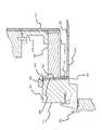
[0040]処理チャンバ205は、処理チャンバ205へのアクセスを提供するガスボックス220を含むことができる。ガスボックス220は、処理チャンバ205へのアクセス部を画定することができ、実施形態において、アクセス部は、ガスボックス220内で中央に画定されるか、または配置され得る。送達管216は、ガスボックス220のアクセス部内に配置または結合されて、RPSユニット210と処理チャンバ205の内部との間の前駆体経路を提供することができる。フランジアダプタ218はまた、RPSユニット210の重量の少なくとも一部を分散させるために、上部プレート220と接触して、送達管216への応力を防止または低減することができる。The
[0041]実施形態において、スペーサ222が、処理チャンバ205の外壁および内壁を少なくとも部分的に画定することができる。ガス分配アセンブリ225が、送達管216に近接して処理チャンバ205内に配置されることができ、ガス分配アセンブリ225は、前駆体またはプラズマ放出物を処理チャンバ205内に分配することができる。ポンピングライナ230が、処理チャンバ205の処理領域内に配置されてもよい。ポンピングライナ230は、未反応の前駆体またはプラズマ放出物を処理チャンバ205から排出させることができる。ポンピングライナ230はさらに、エッチングプロセスでエッチングされた粒子を処理チャンバ205から除去して、その後の処理工程中に粒子が基板上に残らないようにすることができる。[0041] In an embodiment, the
[0042]ペデスタル235が、処理チャンバ205の処理領域に含まれてもよく、エッチングまたは他のプロセス工程中に基板を支持するように構成されてもよい。ペデスタル235は、様々な実施形態において、例えば静電、真空、または重力を含む1つ以上のチャッキング機構を有することができる。ペデスタル235は、実施形態において、回転可能または並進可能であってもよく、ガス分配アセンブリ225に向かって上昇し、またはガス分配アセンブリ225から下降することができる。実施形態において、ペデスタル235は、処理チャンバ205の中へおよび処理チャンバ205から外への基板の移送を助けるための1つ以上のリフトピンを含むことができる。ペデスタル235は、処理工程中に基板温度を維持するための加熱または冷却機構を、さらに含んでもよい。The
[0043]ペデスタル235は、フィラメントを含むはめ込まれた加熱要素を含むことができ、または、適宜に温度を上昇または低下させる温度制御流体を通すように構成された1つ以上の管またはチャネルを含むことができる。ペデスタル235は、セラミックヒータであるかまたはセラミックヒータを含む、基板を支持するためのプラットフォームを含むことができる。セラミックヒータは、実施形態において、約20℃から1000℃を超える温度までを含む特定の動作温度に基板を加熱することができる。さらに、セラミックヒータは、実施形態において、基板を、約50℃より高く、約100℃より高く、約150℃より高く、約200℃より高く、約250℃より高く、約300℃より高く、約350℃より高く、約400℃より高く、約500℃より高く、またはより高く、加熱することができる。さらに、セラミックヒータは、実施形態において、基板温度を、約1000℃未満、約900℃未満、約800℃未満、約700℃未満、約600℃未満、または約500℃未満に維持することができる。セラミックヒータはさらに、基板温度を、実施形態において約100℃~約500℃、または実施形態において約300℃~約500℃に加熱または維持するように構成されてもよい。実施形態において、ヒータは、基板温度を約300℃未満に維持するように構成され、この場合、代替の金属製加熱要素が、セラミックヒータの代わりに使用されてもよい。例えば、コーティングされたアルミニウムヒータが使用されてもよいし、またはアルミニウムもしくは処理されたアルミニウムペデスタル上の埋め込まれたもしくはコーティングされたヒータが、使用されてもよい。[0043] The
[0044]処理チャンバ205の部品は、エッチングまたは他の処理工程中に動作環境に耐えるように構成されてもよい。処理チャンバ205の部品は、例えば硬質の陽極酸化されたアルミニウムを含む陽極酸化または酸化された材料であってもよい。プラズマ放出物または他の腐食性材料と接触し得る処理チャンバ205内の各部品は、腐食しないように保護するため処理またはコーティングされてもよい。いくつかの実施形態では、フッ素または塩素を含むプラズマ放出物による腐食を防止するために、代替材料が利用されてもよい。例えば、処理チャンバ205内の1つ以上の部品が、実施形態において、セラミックまたは石英であってもよい。特定の例として、ガス分配アセンブリ225、スペーサ222、ポンピングライナ230、またはプラズマもしくは非プラズマ前駆体によって接触され得る任意の部品のうちの1つ以上の部品が、石英もしくはセラミックであってもよく、またはそれらを含んでもよい。さらに、送達管216は、石英であってもよいし、または石英を含んでもよく、例えば、送達管216内に石英ライナを含んでもよい。送達管は、実施形態において、アルミニウムまたは硬質の陽極酸化されたアルミニウムであってもよく、石英の内側表面によって特徴付けられてもよい。例えば塩素を含む、RPSユニット210内で解離した前駆体によって引き起こされる腐食から内部部品を保護するために、RPSユニット210が、石英でライニングされてもよい。RPSユニット210は、陽極酸化された金属を含んでもよく、RPSユニット210のチャンバキャビティが、さらに腐食を防止するために、石英でライニングされてもよい。The parts of the
[0045]RPSユニット210からの遠隔プラズマを利用することによって、処理チャンバ205は、プラズマ生成によって引き起こされる内部腐食からさらに保護され得る。実施形態において、処理チャンバ205は、プラズマを生成するように構成されず、プラズマ生成は、RPSユニット210内で処理チャンバ205の外部で実行され得る。実施形態において、容量結合プラズマなど(他のプラズマ源が使用されてもよい)による、追加のプラズマ処理が、処理チャンバ205内で行われてもよい。例えば、ガスボックス220およびガス分配アセンブリ225の1つ以上の部品が、容量結合プラズマが生成され得る電極として利用されてもよい。プラズマ生成から基板との相互作用までの経路長を短縮することによりプラズマ放出物の再結合の面で役に立つように、チャンバ内の追加のまたは代替のプラズマ部品が、使用されてもよい。By utilizing the remote plasma from the
[0046]プラズマによって解離された前駆体は、一定の滞留時間後に再結合する。例えば、塩素系前駆体がRPSユニット210内で解離した後、前駆体またはプラズマ放出物は、送達管216を通って処理チャンバ205に流入し、次にペデスタル235上の基板と相互作用する。ラジカル放出物の移動経路の長さに応じて、放出物またはラジカルは再結合し、ラジカル前駆体の反応性を少なくとも部分的に失い得る。さらに、様々な管またはチャネルを通るなど移動経路が複雑になればなるほど、プラズマ放出物と接触する各部品が、腐食しないよう保護するために処理またはコーティングされ得るので、より多くの保護物が、システム内に含まれ得る。したがって、処理チャンバ205は、RPSユニット210から処理チャンバ205への、次いで排気プレナム230を通る比較的直線的な移動ラインを含み得る。さらに、一旦処理チャンバ205内に入ると、前駆体またはプラズマ放出物は、ガス分配アセンブリ225の1つ以上のインラインの部品を通って移動して、基板に接触することができる。ガス分配アセンブリ225の部品は、基板に向かう流れの均一性を改善するために利用され得るが、それ以外に、処理チャンバ205内の滞留時間ならびにプラズマ放出物の再結合を減少させるための前駆体流路の長さの短縮を維持するために、利用され得る。The precursor dissociated by the plasma recombines after a certain residence time. For example, after the chlorine-based precursor dissociates within the
[0047]図3は、本技術の実施形態による例示的な処理チャンバ205の一部分の概略断面図を示す。図3は、図2のガス分配アセンブリ225の部品の部分図を含み、前述したものと同様の部品を含むことができる。図3に示す処理チャンバ205は、例えば、送達管216、フランジアダプタ218、ガスボックス220、およびスペーサ222を含むことができる。さらに詳しく示されているように、スペーサ222は、ガスボックス220が結合される第1の表面321によって特徴付けられ得る。スペーサ222は、実施形態において、第1の表面321の内側部分に凹状棚部323を画定することができる。内側部分は、例えば、部品に対してもしくはチャンバに対して半径方向に処理チャンバ205の中心軸の方に位置する部分であってもよく、または処理チャンバ205の内部に面する部分であってもよい。図に示されるように、凹状棚部323は、スペーサ222の第1の表面321の、処理チャンバ205の内部に向かう側に形成され、ガスボックス220の結合位置に近接して配置されてもよい。ガスボックス220は、実施形態において、凹状棚部323を少なくとも部分的に覆ってもよく、凹状棚部323を完全に覆ってもよい。FIG. 3 shows a schematic cross-sectional view of a portion of an
[0048]支持ブラケット305が、スペーサ222の凹状棚部323に据え付けられ得る。支持ブラケット305は、スペーサ222の第2の表面324に沿って延びることができる。スペーサ222の第2の表面324は、処理チャンバ205の内部に面し、実施形態において、第1の表面321に隣接するスペーサ222の表面とすることができる。支持ブラケット305は、スペーサ222の第2の表面324に沿って凹状棚部323からほぼまたは本質的に直角に延びることができる。支持ブラケット305は、支持ブラケット305から処理チャンバ205内に延びる支持棚部307を提供する向きに応じて、SまたはZ形状によって特徴付けられてもよい。支持ブラケット305は、環状形状を有し、処理チャンバ205の内部の周りに延びることができる。ガスケットまたはOリング309が、支持ブラケット305に隣接して配置されてもよく、処理チャンバ205の構成において支持ブラケット305から半径方向外側にあってもよい。ガスケット309は、ガスボックス220とスペーサ222との間に配置されて、部品および支持ブラケット305の周りに流体シールを提供することができる。ガスボックス220がスペーサ222と結合されるとき、ガスケットまたはOリング309が圧縮されて、部品間にシールを形成し得る。[0048] The
[0049]さらに図示されるように、ガスボックス220の一部が、ガスボックス220が結合されるスペーサ222の第1の表面321を越えて延びて、スペーサ222の第2の表面324または支持ブラケット305と平行に少なくとも部分的に延びてもよい。図示のように、ガスボックス220の一部が、スペーサ222の第1の表面321の平面を横切って、スペーサ222の第2の表面324と平行に処理チャンバ205内を延びる。ガスボックス220の一部は、処理チャンバ205内のガスボックス220の凹部であってもよく、ガスボックス220の凹部は、スペーサ222の第2の表面324に沿って延びる支持ブラケット305の一部に隣接して配置されてもよい。実施形態において、ガスボックス220は、完全に平行に延びていなくてもよく、スペーサ222の第2の表面324に向かう、またはスペーサ222の第2の表面324から離れるように、ある角度で延びていてもよい。支持ブラケット305は、スペーサ222の第2の表面324と、スペーサ222の第2の表面324と平行に少なくとも部分的に延びるガスボックス220の部分との間に、少なくとも部分的に配置されてもよい。支持ブラケット305は、実施形態において、スペーサ222とガスボックス220との間に間隔を空けて配置されてもよいし、または、スペーサ220の第2の表面324、もしくはスペーサ220の第2の表面324と平行に少なくとも部分的に延びるガスボックス220の部分のうちの一方もしくは両方と直接接触してもよい。As further illustrated, a portion of the
[0050]基板との相互作用のための処理チャンバ205の処理領域への前駆体またはプラズマ放出物の均一な流れを提供するように構成されたガス分配プレート310が、支持ブラケット305に据え付けられてもよい。実施形態において、ガス分配プレート310は、追加の結合材料なしで支持ブラケット305に据え付けられてもよく、支持棚部307に直接据え付けられてもよい。環状ライナ312が、ガス分配プレート310上に据え付けられまたは配置され、支持ブラケット305のさもなければ露出していた領域または内部表面を覆うように、処理チャンバ205の内部の周りに延びることができる。A
[0051]上部プレート314が、環状ライナ312上に配置または据え付けられ、処理チャンバ205の内部に面するガスボックスの表面に近接して配置され得る。上部プレート314は、送達管216からの出口の周りに延びてもよく、前駆体またはプラズマ放出物の流れが、チャンバの内部に面するガスボックス220の表面に接触するのを低減または防止するように、送達管216からの出口に直接接触してもよい。さらに、上部プレート314は、ガスボックス220によって画定されたアクセス部の外径を越えてまたは外径内に延びることができ、送達管216または送達管216の出口に配置されたアダプタと直接接触してもよいし、しなくてもよい。実施形態において、上部プレート314とガスボックス220との間に間隙が存在してもよく、または上部プレート314は、同じ高さで直接に、ガスボックス220と接触してもよい。実施形態において、間隙は、5cm未満であってもよく、約4cm以下、約3cm以下、約2cm以下、約1cm以下、約0.5cm以下、約0.1cm以下、または約0cmであってもよく、0cmの場合、上部プレート314は、ガスボックス220と直接接触する。上部プレート314は、送達管216が上部プレート314と接触するかまたは交わる位置に開孔を画定する平らなプレートであってもよい。上部プレート314は、その他の点では、ガスボックス220を前駆体またはプラズマ放出物への曝露から保護するための中実の設計であってもよい。The
[0052]ガス分配プレート310、環状ライナ312、および上部プレート314のうちの1つ以上が、図2のガス分配アセンブリ225を構成することができる。これらの部品の各々は、プラズマ放出物および前駆体から不活性であるように、またはプラズマ放出物および前駆体からの影響が低減されるように、コーティングまたは設計されてもよい。例えば、ガス分配プレート310、環状ライナ312、および上部プレート314は、それぞれ、実施形態において、石英から作製されるか、もしくは石英を含んでもよいし、または、フッ素もしくは塩素を含む腐食性材料に対して非反応性であるかもしくは反応性が低い材料で作製もしくはコーティングされてもよい。例えば、ガス分配プレート310、環状ライナ312、または上部プレート314のいずれかが、セラミックであってもよく、またはコーティングもしくは陽極酸化されたアルミニウムであってもよい。ガス分配プレート310は、前駆体またはプラズマ放出物を送達管216から処理チャンバ205の処理領域内に均一に分散させることができ、環状ライナ312および上部プレート314は、処理チャンバ内のさらなる部品を保護するために、使用することができる。例えば、前駆体またはプラズマ放出物が、送達管216から分配されると、前駆体は、ガス分配アセンブリ225内で半径方向外側に流れ、ガス分配プレート310と環状ライナ312と上部プレート314との間に画定されるガス分配アセンブリ225のキャビティを少なくとも部分的に満たすことができる。環状ライナ312および上部プレート314は、反応性の前駆体またはプラズマ放出物が、ガス分配プレート310を通って分配されるまたは流される前にガスボックス220および支持ブラケット312に接触することを、防止することができる。One or more of the
[0053]前駆体が、ガス分配プレート310を通って分配されると、流れは、支持ブラケット305またはスペーサ222に少なくとも部分的に接触する可能性がある。この接触は、チャンバを通る加圧されたまたは真空の流れに基づいて最小化され得る。したがって、送達管216とガス分配プレート310との間の処理チャンバ205の領域は、前駆体がガス分配プレート310を通って流れた後よりも、前駆体のチャンバ内での滞留時間が長い場所であり得る。支持ブラケット305およびガスボックス310の内部に面する表面を含む、処理チャンバ205のさもなければ露出していた部分を、それぞれ環状ライナ312および上部プレート314で覆うことによって、チャンバ部品の寿命を改善することができ、処理チャンバ205の寿命にわたって交換コストを低減することができる。スペーサ222および支持ブラケット305の少なくとも一部分が、アルミニウムであってもよく、ガス分配プレート310を通って分配されたまたは流された後の前駆体またはプラズマ放出物と接触し得る。したがって、スペーサ222および支持ブラケット305、またはこれらの部品の少なくとも露出した表面が、それらの劣化を低減するために、硬質の陽極酸化されたアルミニウムなどの材料でコーティングまたは構成され得る。さらに、これらの材料は、石英、セラミック、または他の非反応性材料もしくは低反応性材料から構成されてもよいし、またはそれらを含んでもよい。[0053] Once the precursor has been distributed through the
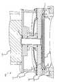
[0054]図4は、本技術の実施形態による例示的な処理チャンバのための送達システム400の概略断面図を示す。図4は、図2および図3に示されたような部品を含むことができ、例えば、RPSユニット210、プラットフォーム212、送達管216、フランジアダプタ218、ガスボックス220および上部プレート314を含むことができる。図示されているように、送達管216は、ガスボックス220によって画定されたアクセス部において処理チャンバ205をRPSユニット210と結合することができる。腐食性であり得るプラズマ放出物への曝露のため、送達管216は、硬質の陽極酸化されたアルミニウムまたはコーティングされたアルミニウムなどの、コーティングまたは保護された材料から構成されるか、またはそれらを含んでもよい。実施形態において、送達管216はまた、プラズマ放出物に曝され得る送達管216の内部に沿って、石英ライナなどのライナを含んでもよい。FIG. 4 shows a schematic cross-sectional view of a
[0055]1つ以上のガスケットまたはOリング405a~cが、RPSユニット210とプラットフォーム212、プラットフォーム212とフランジアダプタ218、フランジアダプタ218とガスボックス220などの部品間に、含まれてもよい。実施形態において、送達管216をRPSユニット210に結合するアダプタ410が、含まれてもよい。アダプタ410は、少なくとも部分的に石英であってもよく、フランジまたはシムを含むことができる。Oリングもしくはガスケット405a、RPSユニット210、またはプラットフォーム212を腐食させる可能性のあるプラズマ放出物によって接触されることから、Oリングまたはガスケット405aを含む部品を保護するために、アダプタ410のフランジまたはシムは、RPSユニット210と送達管216との間の改善されたシールを可能にすることができる。フランジまたはシムは、実施形態において、フォイルOリングであってもよく、または部品間にシールを提供する他の材料であってもよく、さらに、それらは、コーティング、保護層、または材料選択などで、前駆体またはプラズマ放出物による腐食に対して不活性であるか、または腐食から保護されていてもよい。送達管216はまた、送達管216の出口に結合されたアダプタ415を含むことができる。実施形態において、アダプタ415は、ガスボックス220または上部プレート314と結合されてもよい。実施形態において、アダプタ415は、送達管216を通って送達される前駆体またはプラズマ放出物へのガスボックス220の曝露を低減または防止するような形状に作られた、テーパ形状にされた、フランジを付けられた、または他の方法で調整され得る上部プレート314の適合部であってもよい。One or more gaskets or O-
[0056]図5A~図5Bは、本技術の実施形態によるガス分配プレート310の例示的な構造を示す。図5Aに示すように、ガス分配プレート310aは、ガス分配プレート310aの中心軸から半径方向外側に広がる開孔の1つ以上のリングを含むことができる。リングは、ガス分配プレート310aを通る流れの量を調整するためにグループ化されてもよいし間隔を置かれて配置されてもよい任意の数の開孔を含むことができる。図示されているように、ガス分配プレート310aは、開孔の4つのリングを含み、半径方向外側の各リングが、より内側のリングよりも大きな直径によって特徴付けられる開孔を含む。実施形態において、リングの数ならびに開孔のサイズおよび形状の両方に調整を行うことができる。例えば、ガス分配プレートは、ガス分配プレート310aの中心軸から半径方向外側に広がる2,3,4,5,6,7,8,9,10、またはそれより多いリングを有してもよい。さらに、各リングに含まれる開孔の数ならびにリング内の各開孔間の間隔を調整することができる。例えば、各リングは、リングごとに、約3以下、約4以下,約5以下,約6以下,約8以下,約10以下,約15以下,約20以下,約25以下,約30以下,約35以下,約40以下,約45以下,約50以下,約60以下,約70以下,約80以下,約90以下、またはそれより多い開孔を有することができる。さらに、各開孔間の間隔は、リングとリングの間だけでなく、1つのリング内でも、1つの開孔から次の開孔まで同様であっても異なっていてもよい。そのような調整は、ガス分配プレート310aを通る流れを最適化するために使用することができる。5A-5B show exemplary structures of the
[0057]図5Bは、等しいサイズの開孔の複数のリングを有するガス分配プレート310bを示す。図示されているように、1つ以上のリングが、隣接するリングから回転またはオフセットされていてもよい。そのような設計は、ガス分配プレート310bを通るより均一な流れを提供することができる。開孔は、特定のリング内またはリングとリングの間で、ガス分配プレート全体にわたって同様のまたは異なるサイズを有することができる。さらに、開孔間の間隔は、リング内またはリング間で均一であってもよいし、または異なっていてもよい。例えば、例示的なガス分配プレート310bは、約0.1mm~約10mmの均一な開孔サイズを有する複数のリングを含むことができる。開孔サイズは、実施形態において、約1mm~約5mm、または約2mm~約4mmであってもよい。さらに、各リングは、約3~約100個の開孔またはそれより多い開孔を有することができる。例えば、ガス分配プレート310bの内側の方のリングは、より少ない開孔を含むことができ、ガス分配プレート310bの中心から半径方向外側のリングは、より多くの開孔を含むことができる。したがって、リング内の任意の小さな範囲の開孔は、特に、より大きな範囲によって含まれる。図5Aおよび図5Bは、ガス分配プレート210の設計および構成の単なる例であり、開孔の位置、サイズおよび形状に対する任意の数の修正が、本技術によってさらに包含される。[0057] FIG. 5B shows a
[0058]図6は、本技術の実施形態による例示的な処理システム600の一部分の概略断面図を示す。処理システム600は、例えば、図2に示すシステムと同様の部品を含むことができる。処理システム600は、支持部材614を有するプラットフォーム612上に配置された遠隔プラズマ源(「RPS」)ユニット610を含むことができる。RPSユニット610、プラットフォーム612、および支持部材614は、前述したものと同様であってもよい。処理システム600は、追加のフランジアダプタ618によって支持される送達管616をさらに含むことができ、送達管616が、RPSユニット610と結合されてもよい。送達管616およびフランジアダプタ618は、前述したものと同様の特性を有していてもよいが、寸法は、処理チャンバ605との違いに基づいて図2の寸法とは異なっていてもよい。例えば、送達管616およびフランジアダプタ618の両方が、図2に示す処理システムのそれらよりも短い長さ寸法を有してもよい。これらの相違点およびその利点を以下に詳細に説明する。FIG. 6 shows a schematic cross-sectional view of a portion of an
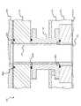
[0059]図2および図3に示すように、処理チャンバ205は、処理チャンバ205内で下げられ、スペーサ222上に配置された支持ブラケット205を有するヒンジ付き設計を含むことができる。次いで、ガスボックス220をそれら部品の上に配置し、スペーサ222と結合させることができる。この設計は、支持ブラケット205を交換のために取り外すこと、ならびに処理チャンバ205の製造中に支持ブラケット205を挿入することを困難にする可能性がある。潜在的に、支持ブラケット205は、最初の配置または交換中に、スペーサ222を引っかく可能性がある。スペーサ222がコーティングまたは陽極酸化仕上げを有する場合、表面欠陥またはスクラッチは、前駆体またはプラズマ放出物と接触した場合に腐食または早期に腐食する場所を、提供し得る。したがって、処理チャンバ605は、製造および交換を容易にするための特徴をさらに含む。As shown in FIGS. 2 and 3, the
[0060]処理チャンバ605は、送達管616のための半導体処理チャンバ605へのアクセス部を画定するガスボックス620を含む。ガスボックス620は、送達管616の遠位領域の周りに結合されてもよく、または送達管616は、実施形態において、ガスボックス620を貫通してもよい。ガスボックス620は、フランジアダプタ618が結合される平坦なまたは実質的に平坦な表面を含むことができる。処理チャンバ605はまた、ガスボックス620の平坦なまたは実質的に平坦な表面の反対側の表面に沿ってガスボックス620に接触する第1の環状支持体622を含むことができる。第1の環状支持体622は、環状支持体の第1の表面でガスボックス620と接触することができる。第1の環状支持体622およびガスボックス620は共同で、処理チャンバの内部領域の周りの第1のチャネル623の少なくとも一部を画定することができる。第1のチャネル623は、ガスボックスと第1の環状支持体との境界面に配置されてもよい。第1の環状支持体622は、第1の環状支持体の内径に凹状棚部を画定することができる。ガスボックス620は、ガスボックス620の平坦または実質的に平坦な表面の反対側の表面内に凹状棚部を画定することができる。ガスボックス620によって画定される凹状棚部は、第1の環状支持体622の凹状棚部の位置と一致するように画定されて、第1のチャネル623を画定することができる。ガス分配アセンブリ625が、第1のチャネル内に配置または据え付けられてもよい。[0060] The
[0061]ガス分配アセンブリ625は、前述のように、ガス分配プレート、環状ライナ、および上部プレートを含んでもよいし、またはより少ない数の部品を含んでもよい。例えば、ガス分配アセンブリ625は、第1のチャネル623内に据え付けられたガス分配プレートであってもよい。実施形態において、環状ライナが、ガス分配プレート上に据え付けられ、上部プレートが、環状ライナ上に据え付けられ、環状ライナと上部プレートの両方が、第1のチャネル623内に少なくとも部分的に据え付けられてもよい。ガス分配アセンブリ625の部品は、第1のチャネル623、ガスボックス620、および第1の環状支持体622の表面を、送達管616を介して送達される前駆体またはプラズマ放出物への曝露から保護するように配置され得る。第1のチャネル623が、ガス分配アセンブリ625と同等の寸法を有し、それゆえ、ガス分配アセンブリは、第1のチャネル623内で同じ高さであってもよい。他の実施形態において、第1のチャネルは、前述のような上部プレートとガスボックス620との間と同様に、ガス分配アセンブリの外径に沿って、1つ以上の間隙を有してもよい。[0061] The
[0062]いくつかの実施形態では、第2の環状支持体624が含まれて、第1の環状支持体622の第1の表面の反対側の第1の環状支持体622の第2の表面で第1の環状支持体622と接触してもよい。第2の環状支持体624は、第1の環状支持体622と同様の形状を有することができる。いくつかの実施形態では、第2の環状支持体624は、第1の環状支持体622よりも大きい厚さを有してもよいし、または小さい厚さを有してもよい。第2の環状支持体624もまた、第1の環状支持体622と同様に、第2の環状支持体の内径に凹状棚部を画定することができる。第1の環状支持体622の第2の表面と共に第2の環状支持体624の凹状棚部は、各々、半導体処理チャンバの内部領域の周りに第2のチャネル626を少なくとも部分的に画定することができる。図示されていないが、第1の環状支持体622もまた、ガスボックス620と同様に、第1の環状支持体の第2の表面内に凹状棚部を画定してもよい。この凹状棚部は、ガス分配アセンブリ625の部品と同様の追加の部品を収容するために、第2のチャネル626の高さを増加させることができる。[0062] In some embodiments, a second
[0063]処理チャンバ605は、第2のチャネル626内に据え付けられた第2のガス分配プレート627を、さらに含むことができる。第2のガス分配プレート627およびガス分配アセンブリ625のガス分配プレートは、同様の設計であっても、異なる設計であってもよく、両方とも、石英または前述したような材料で作製されても、またはそれらを含んでもよい。ガス分配プレートは、互いに同様の開孔配置を有してもよいし、または互いに異なる配置を有してもよく、いずれかまたは両方のガス分配プレートが、図5A~図5Bに関して論じた配置と同様の配置を含んでもよい。例えば、ガス分配アセンブリ625の第1のガス分配プレートおよび第2のガス分配プレート627は、同様の形状によって特徴付けられてもよく、各々、個々のガス分配プレートの周りにリング状に配置された複数の開孔を画定してもよい。実施形態において、プレートは、プレートを通る流れの均一性を向上させるために、整列された開孔を有してもよいし、または互いからオフセットされた開孔を有してもよい。図示されていないが、処理チャンバ605は、ペデスタル、ヒータ、および図2に関連して説明した他の部品をさらに含むことができることを、理解されたい。The
[0064]ガスボックス620、第1の環状支持体622、および第2の環状支持体624は、処理チャンバ605の内部領域または処理領域の寸法を少なくとも部分的に画定するだけでなく、処理チャンバ605の外側寸法を少なくとも部分的に画定するように、同様の外径を有し、積層されてもよい。部品は、図示のように積み重ねられて、第1のチャネル623および第2のチャネル626を画定することができる。この積み重ねられた設計ならびにガスボックス620の平坦な表面は、より短い支持部材614、アダプタフランジ618、および送達管616を可能にし得る。この異なるガスボックス620の設計は、処理チャンバ605の中に延びる凹部を含まないので、これらの部品の高さは、低減され得る。したがって、送達管616は、処理チャンバ605の内部にアクセスするための長さを短くすることができる。送達管の長さを短縮することによって、処理チャンバ605に送達される前駆体またはプラズマ放出物は、基板へのより短い流路を有することができる。流路の長さを短縮することによって、プラズマ前駆体の解離が維持され、エッチングプロセスは、プラズマ放出物生成からエッチングされる基板または材料との接触までのより長い流路を有するチャンバ内で行われる場合よりも、効率的になり得る。The
[0065]図7は、本技術の実施形態による例示的なガス分配プレート725の断面平面図を示す。図は、上述したような、ガス分配プレート725と第1の環状支持体622との結合を、送達管616からの視点と共に示す。図示されているように、ピン631が、第1のチャネル623内のプレートの動きを防止または低減するように、ガス分配プレート725を支持し配置するために、含まれる。図2におけるような支持ブラケットに据え付けられているのとは異なり、第1の環状支持部材622を利用することによって、ガス分配プレート725の適切な位置または向きを保証するように、直接的な接続を行うことができる。処理チャンバ605は、少なくとも1つのピン631を含むことができ、例えば、ガス分配プレート725を第1の環状支持体622に取り外し可能に結合することができるピン631a、631b、631cなどの任意の数のピンを含むことができる。FIG. 7 shows a sectional plan view of an exemplary
[0066]ピンは、実施形態において、第1の環状支持体622を貫通して延びて、追加的に第2のガス分配プレート627を第2の環状支持体624にピン留めしてもよいし、または実施形態において、第1の環状支持体622内で止められてもよい。ピンは、単にプレートを相対位置に保持するだけでもよいし、または特に、結合部材の取り外しなしでの部品の引き出しを防止する、例えばボルト、ネジ等の結合部材などで、プレートを所定の位置に固定してもよい。製造中、ガス分配プレート725は、ガスボックス620が第1の環状支持体622と結合する前に、ピン上に動かされてもよい。その場合、ガス分配プレート725が処理中に動くことを防止または実質的に防止することができ、さもなければ、1つ以上の部品に引っかき傷がついたり、コーティング層または保護層が除去または損傷されたりする可能性がある。[0066] The pin may, in the embodiment, extend through the first
[0067]図8は、本技術の実施形態による例示的な処理チャンバ800の一部分の概略断面図を示す。処理チャンバ800は、図6の処理チャンバ605と同様であってもよく、送達管816、アダプタフランジ818、およびガスボックス820が調整されている。処理システムのいくつかの部品は示されていないが、他の部品は、先に説明した通りであってもよい。示されているように、アダプタフランジ818は、RPSユニットをバイパスし、送達管816および処理チャンバ805に入るように構成された前駆体のためのアクセスを提供するポート825およびチャネル827の少なくとも一部を画定することができる。送達管816もまた、RPSユニットとガスボックス820との間にチャネル827の少なくとも一部分を画定して、半導体処理チャンバ820への前駆体の送達を可能にすることができる。送達管816はまた、RPSユニットからの前駆体またはプラズマ放出物のためのアクセスを提供する1つ以上の開孔828を画定することができる。実施形態において、開孔828は、送達管を回って間隔を空けて配置され、チャネル827を囲んでアクセスを提供することができる。[0067] FIG. 8 shows a schematic cross-sectional view of a portion of an
[0068]インサート829が、図に示すように、送達管816内に配置されてもよい。インサート829は、RPSユニットおよび送達管816のチャネル827の少なくとも一部からインサート829の混合領域830へのアクセスを提供することができる。インサート829の混合領域830は、複数の混合セクションによって特徴付けることができる。第1の混合セクション831は、インサート829の混合領域830へのアクセス部からのテーパ形状によって特徴付けることができる。混合領域へのアクセス部は、実施形態において、送達管816の内径以下の直径を有する。インサート829の混合領域830は、第1の混合セクション831に近接した位置から送達管816の出口までの広がる内径によって特徴付けられる第2の混合セクション833を、さらに含むことができる。[0068] The
[0069]混合領域830は、送達管816の内径よりも小さい内径を有する円筒形状によって特徴付けられる第3の混合セクション835を、さらに含むことができる。例えば、第3の混合セクション835は、送達管816の内径の約90%以下の内径を有してもよい。第3の混合セクション835の内径はまた、実施形態において、送達管816の内径の約85%以下、約80%以下、約75%以下、約65%以下、約60%以下、約55%以下、約50%以下、約45%以下、約40%以下、約35%以下、約30%以下、約25%以下、約20%以下、約15%以下、約10%以下、または約5%以下であってもよい。第3の混合セクションの内径はまた、実施形態において、送達管816の内径の約5%以上、約10%以上、約15%以上、約20%以上、約25%以上、約30%以上、約35%以上、約40%以上、約45%以上、約50%以上、約55%以上、約60%以上、約65%以上、約70%以上、約75%以上、約80%以上、約85%以上、約90%以上、または約95%以上であってもよい。混合セクションおよびインサートを含めることによって、チャネル827を通って導入された前駆体は、処理チャンバ805に入る前に、RPSユニットを通って導入された前駆体またはプラズマ放出物とより均一に混合され得る。[0069] The mixing
[0070]図8に示すように、ガスボックス820は、処理チャンバ805に入るまで、RPSユニットから導入された前駆体またはプラズマ放出物から分離した状態に維持され得るバイパス前駆体のためのさらなるアクセスを可能にするために、複数のプレートで作製されてもよい。ガスボックス820は、実施形態において、互いに連結された第1のガスボックスプレート840および第2のガスボックスプレート842を含むことができる。第2のガスボックスプレート842は、第2のガスボックスプレート842の第2の表面に沿って第1の環状支持体622と少なくとも部分的に接触してもよい。ガスボックスプレート842の第2の表面は、第1のガスボックスプレート840と接触している第2のガスボックスプレート842の第1の表面の反対側であってもよい。第2のガスボックスプレート842は、実施形態において、複合チャネルまたは複数のチャネル845を画定することができる。第1のガスボックスプレート840が第2のガスボックスプレートと結合されるとき、流路が、複合チャネルまたは複数のチャネル845を通って画定され得る。第1のガスボックスプレート840は、複数のチャネル845のうちの少なくとも1つのチャネルへのアクセスを提供するポート847をさらに画定することができる。バイパス前駆体が、ポート847を通って導入され、プラズマ放出物とは別に処理チャンバに流入することができる。As shown in FIG. 8, the
[0071]図9は、本技術の実施形態による例示的なガスボックス820構成の断面平面図を示す。上述したように、ガスボックス820は、互いに結合された第1のガスボックスプレート840と第2のガスボックスプレート842とを含むことができる。ガスボックス820の2つのプレートは、送達管816のためのアクセス部を画定する。複合チャネルと見なされてもよい複数のチャネル845が、第2のガスボックスプレート842内に画定される。第1のガスボックスプレート840のポート847は、複数のチャネル845へのアクセス、およびRPSユニットをバイパスすることができる前駆体のためのポート847からの流路へのアクセスを提供することができる。複数のチャネル845は、ポート847を通って導入された前駆体を処理チャンバ805内により均一に分散させるための流れパターンを提供することができる。複数のチャネル845は、ポート847から導入されたバイパス前駆体の再帰的な流れを複数のチャネル845にわたって生成するように画定されてもよい。FIG. 9 shows a sectional plan view of an
[0072]第2のガスボックスプレート842は、複数のチャネル845から半導体処理チャンバ805の内部領域へのアクセスを提供する、入口チャネルなどの少なくとも1つのチャネル949を、さらに画定することができる。第2のガスボックスプレート842は、処理領域内への前駆体のより均一な流れを提供するための複数のチャネル949を、さらに画定することができる。第2のガスボックスプレート842によって画定されたチャネル949は、実施形態において、第1のガスボックスプレート840によって画定されたポート847の半径方向外側に配置され、または位置してもよい。このような構成は、第2のガスボックスプレート842内のチャネル949を通って処理チャンバ805に入る前に、チャネル845を通る前駆体のより均一な分布を提供することができる。The second
[0073]図10は、本技術の実施形態による例示的なガスボックス820の構成の一部分の断面図を示す。上述したように、ガスボックス820は、第1のガスボックスプレート840と第2のガスボックスプレート842とを含むことができる。第2のガスボックスプレート842は、複数のチャネル845と、前述の処理チャンバ805へのアクセスを提供する1つ以上の入口チャネル949とを、画定することができる。前駆体は、RPSユニットをバイパスし、入口チャネル949を通って処理チャンバに入り、前述のガス分配アセンブリ625などのガス分配アセンブリに接触することができる。ガス分配アセンブリ625は、バイパス前駆体がガス分配アセンブリ625に入り、処理のために基板に分配されることを可能にする1つ以上の開孔1025を含み得る上部プレート1020を含むことができる。さらに、または代わりに、上部プレート1020は、開孔1025を含まなくてもよく、この場合、処理チャンバ949に入るバイパス前駆体は、ガス分配アセンブリ625の周りを通って、処理チャンバの処理領域に入ることができる。ガス分配アセンブリ625が据え付けられることができる第1の環状支持体は、バイパス前駆体がガス分配アセンブリ625を通り過ぎることができるノッチを画定してもよい。その場合、バイパス前駆体は、ガス分配アセンブリ625を通過した後まで、RPSユニットから分配された前駆体またはプラズマ放出物から流体的に分離した状態に維持され得る。実施形態において、ガス分配アセンブリ625はまた、バイパス前駆体が上部プレート1020の開孔1025を通ってガス分配アセンブリ625に確実に入るようにするために、ガスボックス820の側壁と同一平面に位置してもよい。[0073] FIG. 10 shows a cross-sectional view of a part of the configuration of an
[0074]図11は、本技術の実施形態による基板をエッチングする方法1100を示す。方法1100は、工程1110において、プラズマを発生させながら塩素含有前駆体をRPSユニットに送達して、プラズマ放出物を生成することを、含むことができる。工程1120において、プラズマ放出物が、処理チャンバ内に入って、石英ガス分配プレートを通って流されることができる。工程1030において、プラズマ放出物は、処理チャンバ内に収容された基板をエッチングすることができる。処理チャンバは、これまでのセクションで説明したチャンバのいずれかであってよい。エッチング工程は、実施形態において、約300℃~約500℃の温度で実施されてもよく、実施形態において、約300℃未満であってもよい。FIG. 11 shows a
[0075]エッチングプロセスは、RPSユニットをバイパスする1種以上の前駆体を、前述のポートのいずれかを通って導入することを、さらに含むことができる。チャンバは、実施形態において、真空下に維持されてもよく、約1トール以上、例えば約3トールまで、約5トールまで、約10トールまで、約20トールまで、またはそれ以上に加圧されてもよい。前述の図面に関連して記載したチャンバの1つで方法1100を実施する場合、チャンバ部品が、プラズマ放出物から保護されてもよい。その結果、チャンバ部品は、保護されていない部品ほど急速に劣化することがなく、従来のチャンバ部品よりもメンテナンスが少なく、洗浄が少なく、交換回数が少なくて済む可能性がある。さらに、記載されたチャンバは、遠隔プラズマユニットから基板までのより短い流路を可能にし、解離した塩素の再結合が少ないために、エッチング工程の効率を高めることができる。The etching process can further comprise introducing one or more precursors that bypass the RPS unit through any of the aforementioned ports. In embodiments, the chamber may be maintained under vacuum and may be pressurized to about 1 toll or more, such as up to about 3 tolls, up to about 5 tolls, up to about 10 tolls, up to about 20 tolls, or more. May be good. If
[0076]前述の説明では、説明の目的で、本技術の様々な実施形態の理解を提供するために、多くの詳細が述べられている。しかしながら、特定の実施形態は、これらの詳細の一部を伴わずに、または追加の詳細と共に実施され得ることが、当業者には明らかであろう。[0076] In the above description, for purposes of illustration, many details are given to provide an understanding of various embodiments of the present art. However, it will be apparent to those skilled in the art that certain embodiments may be implemented without some of these details or with additional details.
[0077]いくつかの実施形態を開示したが、実施形態の精神から逸脱することなく、様々な修正、代替構成、および均等物を使用できることが、当業者によって理解されるであろう。さらに、いくつかの周知のプロセスおよび要素が、本技術を不必要に不明瞭にすることを避けるために、記載されていない。したがって、上記の説明は、技術の範囲を限定するものと解釈されるべきではない。Although some embodiments have been disclosed, it will be appreciated by those skilled in the art that various modifications, alternative configurations, and equivalents can be used without departing from the spirit of the embodiments. In addition, some well-known processes and elements have not been described to avoid unnecessarily obscuring the technique. Therefore, the above description should not be construed as limiting the scope of the art.
[0078]値の範囲が与えられた場合、その範囲の上限と下限の間の中間にある各値も、文脈上そうでないことが明らかである場合を除いて、下限の単位の最小の端数まで、特に開示されていることが理解される。明示されたある範囲内の任意の明示された値または明示されていない中間の値と、その明示された範囲内の任意の他の明示された値または中間の値との間の、任意のより狭い範囲も包含される。これらのより小さな範囲の上限および下限は、独立に、そのより小さな範囲に含められることもあれば、または除外されることもあり、そのより小さな範囲に上限と下限のうちの一方が含まれるか、いずれも含まれないか、または両方が含まれるような各範囲もまた、その明示された範囲内で除外される限界が特定されることを条件に、本技術の範囲に包含される。明示された範囲が、上限と下限のうちの一方または両方を含む場合、その含まれた上限と下限のうちの一方または両方を除外した範囲もまた、含まれる。Given a range of values, each value in between the upper and lower bounds of the range is also up to the smallest fraction of the lower bound unit, unless it is clear in the context that this is not the case. , Especially disclosed. Any twist between any explicit or unspecified intermediate value within an explicit range and any other explicit or intermediate value within that explicit range. A narrow range is also included. The upper and lower limits of these smaller ranges may be independently included or excluded in the smaller range, and the smaller range contains one of the upper and lower limits. , Each range in which either is not included, or both are included, is also included in the scope of the present art, provided that the limits excluded within the specified scope are specified. If the specified range includes one or both of the upper and lower limits, then the range excluding one or both of the included upper and lower limits is also included.
[0079]本明細書および添付の特許請求の範囲で使用されるとき、単数形「1つの(a)」、「1つの(an)」、および「その(the)」は、文脈上そうでないことが明らかである場合を除き、複数の参照を含む。したがって、例えば、「開孔」と言うときには、複数のそのような開孔が含まれ、「プレート」と言うときには、1つ以上のプレート、および当業者に知られているその均等物が含まれる、等々である。[0079] As used herein and in the appended claims, the singular forms "one (a)", "one (an)", and "the" are not in context. Includes multiple references unless it is clear that. Thus, for example, the term "opening" includes a plurality of such openings, and the term "plate" includes one or more plates and their equivalents known to those of skill in the art. , And so on.
[0080]さらに、本明細書および以下の特許請求の範囲で使用されるとき、「備える(comprise(s))」、「備えている(comprising)」、「含有する(contain(s))」、「含有している(containing)」、「含む(include(s))」、および「含んでいる(including)」という言葉は、明示された特徴、完全体、構成要素または工程の存在を示すことが意図されているが、これらの言葉は、1つ以上の他の特徴、完全体、構成要素、工程、行為またはグループの存在または追加を排除しない。[0080] Further, as used herein and within the scope of the following claims, "comprise (s)", "comprising", "contain (s)". , "Contingent", "include (s)", and "inclusion" indicate the presence of an explicit feature, completeness, component or process. Although intended, these terms do not preclude the existence or addition of one or more other features, perfections, components, processes, acts or groups.
Claims (20)
Translated fromJapanese第1の表面と、当該第1の表面の反対側の第2の表面とを特徴とする第1のガスボックスプレートと、
前記第1のガスボックスプレートの前記第2の表面に沿って前記第1のガスボックスプレートと結合された第2のガスボックスプレートと
を備え、前記第2のガスボックスプレートは、第1の表面と、当該第1の表面の反対側の第2の表面とを特徴とし、前記第2のガスボックスプレートは、前記第2のガスボックスプレートの前記第1の表面内に複数のチャネルを画定し、前記第1のガスボックスプレートの前記第2の表面と前記第2のガスボックスプレートの前記第1の表面とが、前記複数のチャネルを通る流路を画定し、
前記複数のチャネルが互いに流体連通し、前記ガスボックスに沿って半径方向外側に延在する複合チャネルを画定する、半導体処理システム。A semiconductor processing system including a gas box, wherein the gas box is
A first gas box plate characterized by a first surface and a second surface opposite the first surface.
A second gas boxplate coupled to the first gas box plate is provided along the second surface of the first gas box plate, and the second gas box plate is a first surface. And a second surface opposite the first surface, the second gas box plate defines a plurality of channels within the first surface of the second gas box plate. The second surface of the first gas box plate and the first surface of the second gas box plate definea flow path through the plurality of channels.
A semiconductor processing systemin which the plurality of channels fluidly communicate with each other and define a composite channel extending radially outward along the gas box .
第1の表面と、当該第1の表面の反対側の第2の表面とを特徴とする第1のガスボックスプレートと、
前記第1のガスボックスプレートの前記第2の表面に沿って前記第1のガスボックスプレートと結合された第2のガスボックスプレートと
を備え、前記第2のガスボックスプレートは、第1の表面と、当該第1の表面の反対側の第2の表面とを特徴とし、前記第2のガスボックスプレートは、前記第2のガスボックスプレートの前記第1の表面内に複数のチャネルを画定し、前記第1のガスボックスプレートの前記第2の表面と前記第2のガスボックスプレートの前記第1の表面とが、前記複数のチャネルを通る流路を画定し、
前記複数のチャネルが互いに流体連通し、前記ガスボックスに沿って半径方向外側に延在する複合チャネルを画定する、半導体処理システムガスボックス。Semiconductor processing system gas box
A first gas box plate characterized by a first surface and a second surface opposite the first surface.
A second gas boxplate coupled to the first gas box plate is provided along the second surface of the first gas box plate, and the second gas box plate is a first surface. And a second surface opposite the first surface, the second gas box plate defines a plurality of channels within the first surface of the second gas box plate. The second surface of the first gas box plate and the first surface of the second gas box plate definea flow path through the plurality of channels.
A semiconductor processing system gas boxin which the plurality of channels fluidly communicate with each other and define a composite channel extending radially outward along the gas box.
第1の表面と、当該第1の表面の反対側の第2の表面とを特徴とする第1のガスボックスプレートと、 A first gas box plate characterized by a first surface and a second surface opposite the first surface.
前記第1のガスボックスプレートの前記第2の表面に沿って前記第1のガスボックスプレートと結合された第2のガスボックスプレートと With a second gas box plate coupled to the first gas box plate along the second surface of the first gas box plate
を備え、前記第2のガスボックスプレートは、第1の表面と、当該第1の表面の反対側の第2の表面とを特徴とし、前記第2のガスボックスプレートは、前記第2のガスボックスプレートの前記第1の表面内に複数のチャネルを画定し、前記第1のガスボックスプレートの前記第2の表面と前記第2のガスボックスプレートの前記第1の表面とが、前記複数のチャネルを通る流路を画定し、The second gas box plate comprises a first surface and a second surface opposite the first surface, wherein the second gas box plate comprises the second gas. A plurality of channels are defined in the first surface of the box plate, and the second surface of the first gas box plate and the first surface of the second gas box plate are the plurality of. Delimit the flow path through the channel and
前記第1のガスボックスプレートが、前記第1のガスボックスプレートを通って延びるポートを画定し、 The first gas box plate defines a port extending through the first gas box plate.
前記ポートが、前記複数のチャネルの1つ以上のチャネルの半径方向内側で前記複数のチャネルのうちの1つのチャネルへの流体アクセスを提供するように構成されている、半導体処理システム。 A semiconductor processing system in which the port is configured to provide fluid access to one of the plurality of channels within the radial inside of the plurality of channels.
第1の表面と、当該第1の表面の反対側の第2の表面とを特徴とする第1のガスボックスプレートと、 A first gas box plate characterized by a first surface and a second surface opposite the first surface.
前記第1のガスボックスプレートの前記第2の表面に沿って前記第1のガスボックスプレートと結合された第2のガスボックスプレートと With a second gas box plate coupled to the first gas box plate along the second surface of the first gas box plate
を備え、前記第2のガスボックスプレートは、第1の表面と、当該第1の表面の反対側の第2の表面とを特徴とし、前記第2のガスボックスプレートは、前記第2のガスボックスプレートの前記第1の表面内に複数のチャネルを画定し、前記第1のガスボックスプレートの前記第2の表面と前記第2のガスボックスプレートの前記第1の表面とが、前記複数のチャネルを通る流路を画定し、The second gas box plate comprises a first surface and a second surface opposite the first surface, wherein the second gas box plate comprises the second gas. A plurality of channels are defined in the first surface of the box plate, and the second surface of the first gas box plate and the first surface of the second gas box plate are the plurality of. Delimit the flow path through the channel and
前記第1のガスボックスプレートが、前記第1のガスボックスプレートを通って延びるポートを画定し、 The first gas box plate defines a port extending through the first gas box plate.
前記ポートが、前記複数のチャネルの1つ以上のチャネルの半径方向内側で前記複数のチャネルのうちの1つのチャネルへの流体アクセスを提供するように構成されている、半導体処理システムガスボックス。 A semiconductor processing system gas box in which the port is configured to provide fluid access to one of the plurality of channels within the radial inside of the plurality of channels.
Applications Claiming Priority (2)
| Application Number | Priority Date | Filing Date | Title |
|---|---|---|---|
| US15/159,478 | 2016-05-19 | ||
| US15/159,478US10522371B2 (en) | 2016-05-19 | 2016-05-19 | Systems and methods for improved semiconductor etching and component protection |
Related Parent Applications (1)
| Application Number | Title | Priority Date | Filing Date |
|---|---|---|---|
| JP2018560459ADivisionJP6753953B2 (en) | 2016-05-19 | 2017-05-18 | Systems and methods for improved semiconductor etching and component protection |
Publications (2)
| Publication Number | Publication Date |
|---|---|
| JP2020205431A JP2020205431A (en) | 2020-12-24 |
| JP7066792B2true JP7066792B2 (en) | 2022-05-13 |
Family
ID=60326172
Family Applications (2)
| Application Number | Title | Priority Date | Filing Date |
|---|---|---|---|
| JP2018560459AActiveJP6753953B2 (en) | 2016-05-19 | 2017-05-18 | Systems and methods for improved semiconductor etching and component protection |
| JP2020139085AActiveJP7066792B2 (en) | 2016-05-19 | 2020-08-20 | Systems and methods for improved semiconductor etching and component protection |
Family Applications Before (1)
| Application Number | Title | Priority Date | Filing Date |
|---|---|---|---|
| JP2018560459AActiveJP6753953B2 (en) | 2016-05-19 | 2017-05-18 | Systems and methods for improved semiconductor etching and component protection |
Country Status (6)
| Country | Link |
|---|---|
| US (1) | US10522371B2 (en) |
| JP (2) | JP6753953B2 (en) |
| KR (1) | KR102198048B1 (en) |
| CN (2) | CN116913808A (en) |
| TW (2) | TWI847181B (en) |
| WO (1) | WO2017201307A1 (en) |
Families Citing this family (408)
| Publication number | Priority date | Publication date | Assignee | Title |
|---|---|---|---|---|
| US9394608B2 (en) | 2009-04-06 | 2016-07-19 | Asm America, Inc. | Semiconductor processing reactor and components thereof |
| US8802201B2 (en) | 2009-08-14 | 2014-08-12 | Asm America, Inc. | Systems and methods for thin-film deposition of metal oxides using excited nitrogen-oxygen species |
| US10283321B2 (en) | 2011-01-18 | 2019-05-07 | Applied Materials, Inc. | Semiconductor processing system and methods using capacitively coupled plasma |
| US9312155B2 (en) | 2011-06-06 | 2016-04-12 | Asm Japan K.K. | High-throughput semiconductor-processing apparatus equipped with multiple dual-chamber modules |
| US10854498B2 (en) | 2011-07-15 | 2020-12-01 | Asm Ip Holding B.V. | Wafer-supporting device and method for producing same |
| US20130023129A1 (en) | 2011-07-20 | 2013-01-24 | Asm America, Inc. | Pressure transmitter for a semiconductor processing environment |
| US9017481B1 (en) | 2011-10-28 | 2015-04-28 | Asm America, Inc. | Process feed management for semiconductor substrate processing |
| US9373517B2 (en) | 2012-08-02 | 2016-06-21 | Applied Materials, Inc. | Semiconductor processing with DC assisted RF power for improved control |
| US9132436B2 (en) | 2012-09-21 | 2015-09-15 | Applied Materials, Inc. | Chemical control features in wafer process equipment |
| US10714315B2 (en) | 2012-10-12 | 2020-07-14 | Asm Ip Holdings B.V. | Semiconductor reaction chamber showerhead |
| US20160376700A1 (en) | 2013-02-01 | 2016-12-29 | Asm Ip Holding B.V. | System for treatment of deposition reactor |
| US10256079B2 (en) | 2013-02-08 | 2019-04-09 | Applied Materials, Inc. | Semiconductor processing systems having multiple plasma configurations |
| US9362130B2 (en) | 2013-03-01 | 2016-06-07 | Applied Materials, Inc. | Enhanced etching processes using remote plasma sources |
| US10683571B2 (en) | 2014-02-25 | 2020-06-16 | Asm Ip Holding B.V. | Gas supply manifold and method of supplying gases to chamber using same |
| US10167557B2 (en) | 2014-03-18 | 2019-01-01 | Asm Ip Holding B.V. | Gas distribution system, reactor including the system, and methods of using the same |
| US11015245B2 (en) | 2014-03-19 | 2021-05-25 | Asm Ip Holding B.V. | Gas-phase reactor and system having exhaust plenum and components thereof |
| US9309598B2 (en) | 2014-05-28 | 2016-04-12 | Applied Materials, Inc. | Oxide and metal removal |
| US10858737B2 (en) | 2014-07-28 | 2020-12-08 | Asm Ip Holding B.V. | Showerhead assembly and components thereof |
| US9890456B2 (en) | 2014-08-21 | 2018-02-13 | Asm Ip Holding B.V. | Method and system for in situ formation of gas-phase compounds |
| US10941490B2 (en) | 2014-10-07 | 2021-03-09 | Asm Ip Holding B.V. | Multiple temperature range susceptor, assembly, reactor and system including the susceptor, and methods of using the same |
| US9657845B2 (en) | 2014-10-07 | 2017-05-23 | Asm Ip Holding B.V. | Variable conductance gas distribution apparatus and method |
| US9355922B2 (en) | 2014-10-14 | 2016-05-31 | Applied Materials, Inc. | Systems and methods for internal surface conditioning in plasma processing equipment |
| US9966240B2 (en) | 2014-10-14 | 2018-05-08 | Applied Materials, Inc. | Systems and methods for internal surface conditioning assessment in plasma processing equipment |
| US11637002B2 (en) | 2014-11-26 | 2023-04-25 | Applied Materials, Inc. | Methods and systems to enhance process uniformity |
| US10573496B2 (en) | 2014-12-09 | 2020-02-25 | Applied Materials, Inc. | Direct outlet toroidal plasma source |
| US10224210B2 (en) | 2014-12-09 | 2019-03-05 | Applied Materials, Inc. | Plasma processing system with direct outlet toroidal plasma source |
| US11257693B2 (en) | 2015-01-09 | 2022-02-22 | Applied Materials, Inc. | Methods and systems to improve pedestal temperature control |
| US20160225652A1 (en) | 2015-02-03 | 2016-08-04 | Applied Materials, Inc. | Low temperature chuck for plasma processing systems |
| US9728437B2 (en) | 2015-02-03 | 2017-08-08 | Applied Materials, Inc. | High temperature chuck for plasma processing systems |
| US10276355B2 (en) | 2015-03-12 | 2019-04-30 | Asm Ip Holding B.V. | Multi-zone reactor, system including the reactor, and method of using the same |
| US10458018B2 (en) | 2015-06-26 | 2019-10-29 | Asm Ip Holding B.V. | Structures including metal carbide material, devices including the structures, and methods of forming same |
| US10600673B2 (en) | 2015-07-07 | 2020-03-24 | Asm Ip Holding B.V. | Magnetic susceptor to baseplate seal |
| US9741593B2 (en) | 2015-08-06 | 2017-08-22 | Applied Materials, Inc. | Thermal management systems and methods for wafer processing systems |
| US9691645B2 (en) | 2015-08-06 | 2017-06-27 | Applied Materials, Inc. | Bolted wafer chuck thermal management systems and methods for wafer processing systems |
| US9349605B1 (en) | 2015-08-07 | 2016-05-24 | Applied Materials, Inc. | Oxide etch selectivity systems and methods |
| US10504700B2 (en) | 2015-08-27 | 2019-12-10 | Applied Materials, Inc. | Plasma etching systems and methods with secondary plasma injection |
| US10211308B2 (en) | 2015-10-21 | 2019-02-19 | Asm Ip Holding B.V. | NbMC layers |
| US11139308B2 (en) | 2015-12-29 | 2021-10-05 | Asm Ip Holding B.V. | Atomic layer deposition of III-V compounds to form V-NAND devices |
| US10529554B2 (en) | 2016-02-19 | 2020-01-07 | Asm Ip Holding B.V. | Method for forming silicon nitride film selectively on sidewalls or flat surfaces of trenches |
| US10343920B2 (en) | 2016-03-18 | 2019-07-09 | Asm Ip Holding B.V. | Aligned carbon nanotubes |
| US10190213B2 (en) | 2016-04-21 | 2019-01-29 | Asm Ip Holding B.V. | Deposition of metal borides |
| US10865475B2 (en) | 2016-04-21 | 2020-12-15 | Asm Ip Holding B.V. | Deposition of metal borides and silicides |
| US10367080B2 (en) | 2016-05-02 | 2019-07-30 | Asm Ip Holding B.V. | Method of forming a germanium oxynitride film |
| US10032628B2 (en) | 2016-05-02 | 2018-07-24 | Asm Ip Holding B.V. | Source/drain performance through conformal solid state doping |
| US10504754B2 (en) | 2016-05-19 | 2019-12-10 | Applied Materials, Inc. | Systems and methods for improved semiconductor etching and component protection |
| US11453943B2 (en) | 2016-05-25 | 2022-09-27 | Asm Ip Holding B.V. | Method for forming carbon-containing silicon/metal oxide or nitride film by ALD using silicon precursor and hydrocarbon precursor |
| US9865484B1 (en) | 2016-06-29 | 2018-01-09 | Applied Materials, Inc. | Selective etch using material modification and RF pulsing |
| US9859151B1 (en) | 2016-07-08 | 2018-01-02 | Asm Ip Holding B.V. | Selective film deposition method to form air gaps |
| US10612137B2 (en) | 2016-07-08 | 2020-04-07 | Asm Ip Holdings B.V. | Organic reactants for atomic layer deposition |
| US10714385B2 (en) | 2016-07-19 | 2020-07-14 | Asm Ip Holding B.V. | Selective deposition of tungsten |
| US9812320B1 (en) | 2016-07-28 | 2017-11-07 | Asm Ip Holding B.V. | Method and apparatus for filling a gap |
| US9887082B1 (en) | 2016-07-28 | 2018-02-06 | Asm Ip Holding B.V. | Method and apparatus for filling a gap |
| KR102532607B1 (en) | 2016-07-28 | 2023-05-15 | 에이에스엠 아이피 홀딩 비.브이. | Substrate processing apparatus and method of operating the same |
| US10062575B2 (en) | 2016-09-09 | 2018-08-28 | Applied Materials, Inc. | Poly directional etch by oxidation |
| US10629473B2 (en) | 2016-09-09 | 2020-04-21 | Applied Materials, Inc. | Footing removal for nitride spacer |
| US9934942B1 (en) | 2016-10-04 | 2018-04-03 | Applied Materials, Inc. | Chamber with flow-through source |
| US10062585B2 (en) | 2016-10-04 | 2018-08-28 | Applied Materials, Inc. | Oxygen compatible plasma source |
| US10546729B2 (en) | 2016-10-04 | 2020-01-28 | Applied Materials, Inc. | Dual-channel showerhead with improved profile |
| US10062579B2 (en) | 2016-10-07 | 2018-08-28 | Applied Materials, Inc. | Selective SiN lateral recess |
| US9947549B1 (en) | 2016-10-10 | 2018-04-17 | Applied Materials, Inc. | Cobalt-containing material removal |
| US10643826B2 (en) | 2016-10-26 | 2020-05-05 | Asm Ip Holdings B.V. | Methods for thermally calibrating reaction chambers |
| US11532757B2 (en) | 2016-10-27 | 2022-12-20 | Asm Ip Holding B.V. | Deposition of charge trapping layers |
| US10229833B2 (en) | 2016-11-01 | 2019-03-12 | Asm Ip Holding B.V. | Methods for forming a transition metal nitride film on a substrate by atomic layer deposition and related semiconductor device structures |
| US10714350B2 (en) | 2016-11-01 | 2020-07-14 | ASM IP Holdings, B.V. | Methods for forming a transition metal niobium nitride film on a substrate by atomic layer deposition and related semiconductor device structures |
| US10643904B2 (en) | 2016-11-01 | 2020-05-05 | Asm Ip Holdings B.V. | Methods for forming a semiconductor device and related semiconductor device structures |
| US10134757B2 (en) | 2016-11-07 | 2018-11-20 | Asm Ip Holding B.V. | Method of processing a substrate and a device manufactured by using the method |
| US10163696B2 (en) | 2016-11-11 | 2018-12-25 | Applied Materials, Inc. | Selective cobalt removal for bottom up gapfill |
| US9768034B1 (en) | 2016-11-11 | 2017-09-19 | Applied Materials, Inc. | Removal methods for high aspect ratio structures |
| US10242908B2 (en) | 2016-11-14 | 2019-03-26 | Applied Materials, Inc. | Airgap formation with damage-free copper |
| US10026621B2 (en) | 2016-11-14 | 2018-07-17 | Applied Materials, Inc. | SiN spacer profile patterning |
| KR102546317B1 (en) | 2016-11-15 | 2023-06-21 | 에이에스엠 아이피 홀딩 비.브이. | Gas supply unit and substrate processing apparatus including the same |
| KR102762543B1 (en) | 2016-12-14 | 2025-02-05 | 에이에스엠 아이피 홀딩 비.브이. | Substrate processing apparatus |
| US11581186B2 (en) | 2016-12-15 | 2023-02-14 | Asm Ip Holding B.V. | Sequential infiltration synthesis apparatus |
| US11447861B2 (en) | 2016-12-15 | 2022-09-20 | Asm Ip Holding B.V. | Sequential infiltration synthesis apparatus and a method of forming a patterned structure |
| KR102700194B1 (en) | 2016-12-19 | 2024-08-28 | 에이에스엠 아이피 홀딩 비.브이. | Substrate processing apparatus |
| US10269558B2 (en) | 2016-12-22 | 2019-04-23 | Asm Ip Holding B.V. | Method of forming a structure on a substrate |
| US10566206B2 (en) | 2016-12-27 | 2020-02-18 | Applied Materials, Inc. | Systems and methods for anisotropic material breakthrough |
| US10867788B2 (en) | 2016-12-28 | 2020-12-15 | Asm Ip Holding B.V. | Method of forming a structure on a substrate |
| US11390950B2 (en) | 2017-01-10 | 2022-07-19 | Asm Ip Holding B.V. | Reactor system and method to reduce residue buildup during a film deposition process |
| US10431429B2 (en) | 2017-02-03 | 2019-10-01 | Applied Materials, Inc. | Systems and methods for radial and azimuthal control of plasma uniformity |
| US10403507B2 (en) | 2017-02-03 | 2019-09-03 | Applied Materials, Inc. | Shaped etch profile with oxidation |
| US10043684B1 (en) | 2017-02-06 | 2018-08-07 | Applied Materials, Inc. | Self-limiting atomic thermal etching systems and methods |
| US10319739B2 (en) | 2017-02-08 | 2019-06-11 | Applied Materials, Inc. | Accommodating imperfectly aligned memory holes |
| US10655221B2 (en) | 2017-02-09 | 2020-05-19 | Asm Ip Holding B.V. | Method for depositing oxide film by thermal ALD and PEALD |
| US10468261B2 (en) | 2017-02-15 | 2019-11-05 | Asm Ip Holding B.V. | Methods for forming a metallic film on a substrate by cyclical deposition and related semiconductor device structures |
| US10943834B2 (en) | 2017-03-13 | 2021-03-09 | Applied Materials, Inc. | Replacement contact process |
| US10529563B2 (en) | 2017-03-29 | 2020-01-07 | Asm Ip Holdings B.V. | Method for forming doped metal oxide films on a substrate by cyclical deposition and related semiconductor device structures |
| USD876504S1 (en) | 2017-04-03 | 2020-02-25 | Asm Ip Holding B.V. | Exhaust flow control ring for semiconductor deposition apparatus |
| US10319649B2 (en) | 2017-04-11 | 2019-06-11 | Applied Materials, Inc. | Optical emission spectroscopy (OES) for remote plasma monitoring |
| KR102457289B1 (en) | 2017-04-25 | 2022-10-21 | 에이에스엠 아이피 홀딩 비.브이. | Method for depositing a thin film and manufacturing a semiconductor device |
| US10770286B2 (en) | 2017-05-08 | 2020-09-08 | Asm Ip Holdings B.V. | Methods for selectively forming a silicon nitride film on a substrate and related semiconductor device structures |
| US10892156B2 (en) | 2017-05-08 | 2021-01-12 | Asm Ip Holding B.V. | Methods for forming a silicon nitride film on a substrate and related semiconductor device structures |
| US11276559B2 (en) | 2017-05-17 | 2022-03-15 | Applied Materials, Inc. | Semiconductor processing chamber for multiple precursor flow |
| JP7176860B6 (en)* | 2017-05-17 | 2022-12-16 | アプライド マテリアルズ インコーポレイテッド | Semiconductor processing chamber to improve precursor flow |
| US11276590B2 (en) | 2017-05-17 | 2022-03-15 | Applied Materials, Inc. | Multi-zone semiconductor substrate supports |
| US10497579B2 (en) | 2017-05-31 | 2019-12-03 | Applied Materials, Inc. | Water-free etching methods |
| US10049891B1 (en) | 2017-05-31 | 2018-08-14 | Applied Materials, Inc. | Selective in situ cobalt residue removal |
| US10920320B2 (en) | 2017-06-16 | 2021-02-16 | Applied Materials, Inc. | Plasma health determination in semiconductor substrate processing reactors |
| US12040200B2 (en) | 2017-06-20 | 2024-07-16 | Asm Ip Holding B.V. | Semiconductor processing apparatus and methods for calibrating a semiconductor processing apparatus |
| US10541246B2 (en) | 2017-06-26 | 2020-01-21 | Applied Materials, Inc. | 3D flash memory cells which discourage cross-cell electrical tunneling |
| US11306395B2 (en) | 2017-06-28 | 2022-04-19 | Asm Ip Holding B.V. | Methods for depositing a transition metal nitride film on a substrate by atomic layer deposition and related deposition apparatus |
| US10685834B2 (en) | 2017-07-05 | 2020-06-16 | Asm Ip Holdings B.V. | Methods for forming a silicon germanium tin layer and related semiconductor device structures |
| US10727080B2 (en) | 2017-07-07 | 2020-07-28 | Applied Materials, Inc. | Tantalum-containing material removal |
| US10541184B2 (en) | 2017-07-11 | 2020-01-21 | Applied Materials, Inc. | Optical emission spectroscopic techniques for monitoring etching |
| US10354889B2 (en) | 2017-07-17 | 2019-07-16 | Applied Materials, Inc. | Non-halogen etching of silicon-containing materials |
| KR20190009245A (en) | 2017-07-18 | 2019-01-28 | 에이에스엠 아이피 홀딩 비.브이. | Methods for forming a semiconductor device structure and related semiconductor device structures |
| US10541333B2 (en) | 2017-07-19 | 2020-01-21 | Asm Ip Holding B.V. | Method for depositing a group IV semiconductor and related semiconductor device structures |
| US11018002B2 (en) | 2017-07-19 | 2021-05-25 | Asm Ip Holding B.V. | Method for selectively depositing a Group IV semiconductor and related semiconductor device structures |
| US11374112B2 (en) | 2017-07-19 | 2022-06-28 | Asm Ip Holding B.V. | Method for depositing a group IV semiconductor and related semiconductor device structures |
| US10590535B2 (en) | 2017-07-26 | 2020-03-17 | Asm Ip Holdings B.V. | Chemical treatment, deposition and/or infiltration apparatus and method for using the same |
| US10170336B1 (en) | 2017-08-04 | 2019-01-01 | Applied Materials, Inc. | Methods for anisotropic control of selective silicon removal |
| TWI815813B (en) | 2017-08-04 | 2023-09-21 | 荷蘭商Asm智慧財產控股公司 | Showerhead assembly for distributing a gas within a reaction chamber |
| US10043674B1 (en) | 2017-08-04 | 2018-08-07 | Applied Materials, Inc. | Germanium etching systems and methods |
| US10297458B2 (en) | 2017-08-07 | 2019-05-21 | Applied Materials, Inc. | Process window widening using coated parts in plasma etch processes |
| US10692741B2 (en) | 2017-08-08 | 2020-06-23 | Asm Ip Holdings B.V. | Radiation shield |
| US10770336B2 (en) | 2017-08-08 | 2020-09-08 | Asm Ip Holding B.V. | Substrate lift mechanism and reactor including same |
| US10249524B2 (en) | 2017-08-09 | 2019-04-02 | Asm Ip Holding B.V. | Cassette holder assembly for a substrate cassette and holding member for use in such assembly |
| US11139191B2 (en) | 2017-08-09 | 2021-10-05 | Asm Ip Holding B.V. | Storage apparatus for storing cassettes for substrates and processing apparatus equipped therewith |
| US11769682B2 (en) | 2017-08-09 | 2023-09-26 | Asm Ip Holding B.V. | Storage apparatus for storing cassettes for substrates and processing apparatus equipped therewith |
| USD900036S1 (en) | 2017-08-24 | 2020-10-27 | Asm Ip Holding B.V. | Heater electrical connector and adapter |
| US11830730B2 (en) | 2017-08-29 | 2023-11-28 | Asm Ip Holding B.V. | Layer forming method and apparatus |
| US11295980B2 (en) | 2017-08-30 | 2022-04-05 | Asm Ip Holding B.V. | Methods for depositing a molybdenum metal film over a dielectric surface of a substrate by a cyclical deposition process and related semiconductor device structures |
| KR102491945B1 (en) | 2017-08-30 | 2023-01-26 | 에이에스엠 아이피 홀딩 비.브이. | Substrate processing apparatus |
| US11056344B2 (en) | 2017-08-30 | 2021-07-06 | Asm Ip Holding B.V. | Layer forming method |
| KR102401446B1 (en) | 2017-08-31 | 2022-05-24 | 에이에스엠 아이피 홀딩 비.브이. | Substrate processing apparatus |
| KR102630301B1 (en) | 2017-09-21 | 2024-01-29 | 에이에스엠 아이피 홀딩 비.브이. | Method of sequential infiltration synthesis treatment of infiltrateable material and structures and devices formed using same |
| US10844484B2 (en) | 2017-09-22 | 2020-11-24 | Asm Ip Holding B.V. | Apparatus for dispensing a vapor phase reactant to a reaction chamber and related methods |
| US10658205B2 (en) | 2017-09-28 | 2020-05-19 | Asm Ip Holdings B.V. | Chemical dispensing apparatus and methods for dispensing a chemical to a reaction chamber |
| US10403504B2 (en) | 2017-10-05 | 2019-09-03 | Asm Ip Holding B.V. | Method for selectively depositing a metallic film on a substrate |
| US10319588B2 (en) | 2017-10-10 | 2019-06-11 | Asm Ip Holding B.V. | Method for depositing a metal chalcogenide on a substrate by cyclical deposition |
| US10424487B2 (en) | 2017-10-24 | 2019-09-24 | Applied Materials, Inc. | Atomic layer etching processes |
| US10283324B1 (en) | 2017-10-24 | 2019-05-07 | Applied Materials, Inc. | Oxygen treatment for nitride etching |
| US10128086B1 (en) | 2017-10-24 | 2018-11-13 | Applied Materials, Inc. | Silicon pretreatment for nitride removal |
| US10923344B2 (en) | 2017-10-30 | 2021-02-16 | Asm Ip Holding B.V. | Methods for forming a semiconductor structure and related semiconductor structures |
| US10910262B2 (en) | 2017-11-16 | 2021-02-02 | Asm Ip Holding B.V. | Method of selectively depositing a capping layer structure on a semiconductor device structure |
| KR102443047B1 (en) | 2017-11-16 | 2022-09-14 | 에이에스엠 아이피 홀딩 비.브이. | Method of processing a substrate and a device manufactured by the same |
| US11022879B2 (en) | 2017-11-24 | 2021-06-01 | Asm Ip Holding B.V. | Method of forming an enhanced unexposed photoresist layer |
| CN111344522B (en) | 2017-11-27 | 2022-04-12 | 阿斯莫Ip控股公司 | Including clean mini-environment device |
| WO2019103613A1 (en) | 2017-11-27 | 2019-05-31 | Asm Ip Holding B.V. | A storage device for storing wafer cassettes for use with a batch furnace |
| US10256112B1 (en) | 2017-12-08 | 2019-04-09 | Applied Materials, Inc. | Selective tungsten removal |
| US10903054B2 (en)* | 2017-12-19 | 2021-01-26 | Applied Materials, Inc. | Multi-zone gas distribution systems and methods |
| US11328909B2 (en) | 2017-12-22 | 2022-05-10 | Applied Materials, Inc. | Chamber conditioning and removal processes |
| US10854426B2 (en) | 2018-01-08 | 2020-12-01 | Applied Materials, Inc. | Metal recess for semiconductor structures |
| US10872771B2 (en) | 2018-01-16 | 2020-12-22 | Asm Ip Holding B. V. | Method for depositing a material film on a substrate within a reaction chamber by a cyclical deposition process and related device structures |
| KR102695659B1 (en) | 2018-01-19 | 2024-08-14 | 에이에스엠 아이피 홀딩 비.브이. | Method for depositing a gap filling layer by plasma assisted deposition |
| TWI799494B (en) | 2018-01-19 | 2023-04-21 | 荷蘭商Asm 智慧財產控股公司 | Deposition method |
| USD903477S1 (en) | 2018-01-24 | 2020-12-01 | Asm Ip Holdings B.V. | Metal clamp |
| US11018047B2 (en) | 2018-01-25 | 2021-05-25 | Asm Ip Holding B.V. | Hybrid lift pin |
| USD880437S1 (en) | 2018-02-01 | 2020-04-07 | Asm Ip Holding B.V. | Gas supply plate for semiconductor manufacturing apparatus |
| US11081345B2 (en) | 2018-02-06 | 2021-08-03 | Asm Ip Holding B.V. | Method of post-deposition treatment for silicon oxide film |
| US10896820B2 (en) | 2018-02-14 | 2021-01-19 | Asm Ip Holding B.V. | Method for depositing a ruthenium-containing film on a substrate by a cyclical deposition process |
| WO2019158960A1 (en) | 2018-02-14 | 2019-08-22 | Asm Ip Holding B.V. | A method for depositing a ruthenium-containing film on a substrate by a cyclical deposition process |
| US10731249B2 (en) | 2018-02-15 | 2020-08-04 | Asm Ip Holding B.V. | Method of forming a transition metal containing film on a substrate by a cyclical deposition process, a method for supplying a transition metal halide compound to a reaction chamber, and related vapor deposition apparatus |
| US10679870B2 (en) | 2018-02-15 | 2020-06-09 | Applied Materials, Inc. | Semiconductor processing chamber multistage mixing apparatus |
| US10964512B2 (en) | 2018-02-15 | 2021-03-30 | Applied Materials, Inc. | Semiconductor processing chamber multistage mixing apparatus and methods |
| US10658181B2 (en) | 2018-02-20 | 2020-05-19 | Asm Ip Holding B.V. | Method of spacer-defined direct patterning in semiconductor fabrication |
| KR102636427B1 (en)* | 2018-02-20 | 2024-02-13 | 에이에스엠 아이피 홀딩 비.브이. | Substrate processing method and apparatus |
| US10975470B2 (en) | 2018-02-23 | 2021-04-13 | Asm Ip Holding B.V. | Apparatus for detecting or monitoring for a chemical precursor in a high temperature environment |
| TWI766433B (en) | 2018-02-28 | 2022-06-01 | 美商應用材料股份有限公司 | Systems and methods to form airgaps |
| US10593560B2 (en) | 2018-03-01 | 2020-03-17 | Applied Materials, Inc. | Magnetic induction plasma source for semiconductor processes and equipment |
| US11473195B2 (en) | 2018-03-01 | 2022-10-18 | Asm Ip Holding B.V. | Semiconductor processing apparatus and a method for processing a substrate |
| US11629406B2 (en) | 2018-03-09 | 2023-04-18 | Asm Ip Holding B.V. | Semiconductor processing apparatus comprising one or more pyrometers for measuring a temperature of a substrate during transfer of the substrate |
| US10319600B1 (en) | 2018-03-12 | 2019-06-11 | Applied Materials, Inc. | Thermal silicon etch |
| US10497573B2 (en) | 2018-03-13 | 2019-12-03 | Applied Materials, Inc. | Selective atomic layer etching of semiconductor materials |
| US11114283B2 (en) | 2018-03-16 | 2021-09-07 | Asm Ip Holding B.V. | Reactor, system including the reactor, and methods of manufacturing and using same |
| KR102646467B1 (en) | 2018-03-27 | 2024-03-11 | 에이에스엠 아이피 홀딩 비.브이. | Method of forming an electrode on a substrate and a semiconductor device structure including an electrode |
| US11230766B2 (en) | 2018-03-29 | 2022-01-25 | Asm Ip Holding B.V. | Substrate processing apparatus and method |
| US11088002B2 (en) | 2018-03-29 | 2021-08-10 | Asm Ip Holding B.V. | Substrate rack and a substrate processing system and method |
| KR102501472B1 (en) | 2018-03-30 | 2023-02-20 | 에이에스엠 아이피 홀딩 비.브이. | Substrate processing method |
| US10573527B2 (en) | 2018-04-06 | 2020-02-25 | Applied Materials, Inc. | Gas-phase selective etching systems and methods |
| KR102600229B1 (en) | 2018-04-09 | 2023-11-10 | 에이에스엠 아이피 홀딩 비.브이. | Substrate supporting device, substrate processing apparatus including the same and substrate processing method |
| US10490406B2 (en) | 2018-04-10 | 2019-11-26 | Appled Materials, Inc. | Systems and methods for material breakthrough |
| US10699879B2 (en) | 2018-04-17 | 2020-06-30 | Applied Materials, Inc. | Two piece electrode assembly with gap for plasma control |
| US10886137B2 (en) | 2018-04-30 | 2021-01-05 | Applied Materials, Inc. | Selective nitride removal |
| TWI811348B (en) | 2018-05-08 | 2023-08-11 | 荷蘭商Asm 智慧財產控股公司 | Methods for depositing an oxide film on a substrate by a cyclical deposition process and related device structures |
| US12025484B2 (en) | 2018-05-08 | 2024-07-02 | Asm Ip Holding B.V. | Thin film forming method |
| US12272527B2 (en) | 2018-05-09 | 2025-04-08 | Asm Ip Holding B.V. | Apparatus for use with hydrogen radicals and method of using same |
| KR20190129718A (en) | 2018-05-11 | 2019-11-20 | 에이에스엠 아이피 홀딩 비.브이. | Methods for forming a doped metal carbide film on a substrate and related semiconductor device structures |
| KR102596988B1 (en) | 2018-05-28 | 2023-10-31 | 에이에스엠 아이피 홀딩 비.브이. | Method of processing a substrate and a device manufactured by the same |
| US11718913B2 (en) | 2018-06-04 | 2023-08-08 | Asm Ip Holding B.V. | Gas distribution system and reactor system including same |
| TWI840362B (en) | 2018-06-04 | 2024-05-01 | 荷蘭商Asm Ip私人控股有限公司 | Wafer handling chamber with moisture reduction |
| US11286562B2 (en) | 2018-06-08 | 2022-03-29 | Asm Ip Holding B.V. | Gas-phase chemical reactor and method of using same |
| US10797133B2 (en) | 2018-06-21 | 2020-10-06 | Asm Ip Holding B.V. | Method for depositing a phosphorus doped silicon arsenide film and related semiconductor device structures |
| KR102568797B1 (en) | 2018-06-21 | 2023-08-21 | 에이에스엠 아이피 홀딩 비.브이. | Substrate processing system |
| TWI873894B (en) | 2018-06-27 | 2025-02-21 | 荷蘭商Asm Ip私人控股有限公司 | Cyclic deposition methods for forming metal-containing material and films and structures including the metal-containing material |
| KR102854019B1 (en) | 2018-06-27 | 2025-09-02 | 에이에스엠 아이피 홀딩 비.브이. | Periodic deposition method for forming a metal-containing material and films and structures comprising the metal-containing material |
| US10612136B2 (en) | 2018-06-29 | 2020-04-07 | ASM IP Holding, B.V. | Temperature-controlled flange and reactor system including same |
| KR102686758B1 (en) | 2018-06-29 | 2024-07-18 | 에이에스엠 아이피 홀딩 비.브이. | Method for depositing a thin film and manufacturing a semiconductor device |
| US10755922B2 (en) | 2018-07-03 | 2020-08-25 | Asm Ip Holding B.V. | Method for depositing silicon-free carbon-containing film as gap-fill layer by pulse plasma-assisted deposition |
| US10388513B1 (en) | 2018-07-03 | 2019-08-20 | Asm Ip Holding B.V. | Method for depositing silicon-free carbon-containing film as gap-fill layer by pulse plasma-assisted deposition |
| US10872778B2 (en) | 2018-07-06 | 2020-12-22 | Applied Materials, Inc. | Systems and methods utilizing solid-phase etchants |
| US10755941B2 (en) | 2018-07-06 | 2020-08-25 | Applied Materials, Inc. | Self-limiting selective etching systems and methods |
| US10767789B2 (en) | 2018-07-16 | 2020-09-08 | Asm Ip Holding B.V. | Diaphragm valves, valve components, and methods for forming valve components |
| US10672642B2 (en) | 2018-07-24 | 2020-06-02 | Applied Materials, Inc. | Systems and methods for pedestal configuration |
| US11053591B2 (en) | 2018-08-06 | 2021-07-06 | Asm Ip Holding B.V. | Multi-port gas injection system and reactor system including same |
| US10883175B2 (en) | 2018-08-09 | 2021-01-05 | Asm Ip Holding B.V. | Vertical furnace for processing substrates and a liner for use therein |
| US10829852B2 (en) | 2018-08-16 | 2020-11-10 | Asm Ip Holding B.V. | Gas distribution device for a wafer processing apparatus |
| US11430674B2 (en) | 2018-08-22 | 2022-08-30 | Asm Ip Holding B.V. | Sensor array, apparatus for dispensing a vapor phase reactant to a reaction chamber and related methods |
| KR102707956B1 (en) | 2018-09-11 | 2024-09-19 | 에이에스엠 아이피 홀딩 비.브이. | Method for deposition of a thin film |
| US11024523B2 (en) | 2018-09-11 | 2021-06-01 | Asm Ip Holding B.V. | Substrate processing apparatus and method |
| US11049751B2 (en) | 2018-09-14 | 2021-06-29 | Asm Ip Holding B.V. | Cassette supply system to store and handle cassettes and processing apparatus equipped therewith |
| US11049755B2 (en) | 2018-09-14 | 2021-06-29 | Applied Materials, Inc. | Semiconductor substrate supports with embedded RF shield |
| US10892198B2 (en) | 2018-09-14 | 2021-01-12 | Applied Materials, Inc. | Systems and methods for improved performance in semiconductor processing |
| US11062887B2 (en) | 2018-09-17 | 2021-07-13 | Applied Materials, Inc. | High temperature RF heater pedestals |
| US11417534B2 (en) | 2018-09-21 | 2022-08-16 | Applied Materials, Inc. | Selective material removal |
| CN110970344B (en) | 2018-10-01 | 2024-10-25 | Asmip控股有限公司 | Substrate holding apparatus, system comprising the same and method of using the same |
| US11232963B2 (en) | 2018-10-03 | 2022-01-25 | Asm Ip Holding B.V. | Substrate processing apparatus and method |
| KR102592699B1 (en) | 2018-10-08 | 2023-10-23 | 에이에스엠 아이피 홀딩 비.브이. | Substrate support unit and apparatuses for depositing thin film and processing the substrate including the same |
| US10847365B2 (en) | 2018-10-11 | 2020-11-24 | Asm Ip Holding B.V. | Method of forming conformal silicon carbide film by cyclic CVD |
| US11682560B2 (en) | 2018-10-11 | 2023-06-20 | Applied Materials, Inc. | Systems and methods for hafnium-containing film removal |
| US10811256B2 (en) | 2018-10-16 | 2020-10-20 | Asm Ip Holding B.V. | Method for etching a carbon-containing feature |
| KR102546322B1 (en) | 2018-10-19 | 2023-06-21 | 에이에스엠 아이피 홀딩 비.브이. | Substrate processing apparatus and substrate processing method |
| KR102605121B1 (en) | 2018-10-19 | 2023-11-23 | 에이에스엠 아이피 홀딩 비.브이. | Substrate processing apparatus and substrate processing method |
| US11121002B2 (en) | 2018-10-24 | 2021-09-14 | Applied Materials, Inc. | Systems and methods for etching metals and metal derivatives |
| USD948463S1 (en) | 2018-10-24 | 2022-04-12 | Asm Ip Holding B.V. | Susceptor for semiconductor substrate supporting apparatus |
| US12378665B2 (en) | 2018-10-26 | 2025-08-05 | Asm Ip Holding B.V. | High temperature coatings for a preclean and etch apparatus and related methods |
| US11087997B2 (en) | 2018-10-31 | 2021-08-10 | Asm Ip Holding B.V. | Substrate processing apparatus for processing substrates |
| KR102748291B1 (en) | 2018-11-02 | 2024-12-31 | 에이에스엠 아이피 홀딩 비.브이. | Substrate support unit and substrate processing apparatus including the same |
| US11572620B2 (en) | 2018-11-06 | 2023-02-07 | Asm Ip Holding B.V. | Methods for selectively depositing an amorphous silicon film on a substrate |
| US11031242B2 (en) | 2018-11-07 | 2021-06-08 | Asm Ip Holding B.V. | Methods for depositing a boron doped silicon germanium film |
| US10847366B2 (en) | 2018-11-16 | 2020-11-24 | Asm Ip Holding B.V. | Methods for depositing a transition metal chalcogenide film on a substrate by a cyclical deposition process |
| US10818758B2 (en) | 2018-11-16 | 2020-10-27 | Asm Ip Holding B.V. | Methods for forming a metal silicate film on a substrate in a reaction chamber and related semiconductor device structures |
| US10559458B1 (en) | 2018-11-26 | 2020-02-11 | Asm Ip Holding B.V. | Method of forming oxynitride film |
| US11437242B2 (en) | 2018-11-27 | 2022-09-06 | Applied Materials, Inc. | Selective removal of silicon-containing materials |
| US12040199B2 (en) | 2018-11-28 | 2024-07-16 | Asm Ip Holding B.V. | Substrate processing apparatus for processing substrates |
| US11217444B2 (en) | 2018-11-30 | 2022-01-04 | Asm Ip Holding B.V. | Method for forming an ultraviolet radiation responsive metal oxide-containing film |
| KR102636428B1 (en) | 2018-12-04 | 2024-02-13 | 에이에스엠 아이피 홀딩 비.브이. | A method for cleaning a substrate processing apparatus |
| US11694879B2 (en)* | 2018-12-07 | 2023-07-04 | Applied Materials, Inc. | Component, method of manufacturing the component, and method of cleaning the component |
| US11158513B2 (en) | 2018-12-13 | 2021-10-26 | Asm Ip Holding B.V. | Methods for forming a rhenium-containing film on a substrate by a cyclical deposition process and related semiconductor device structures |
| TWI874340B (en) | 2018-12-14 | 2025-03-01 | 荷蘭商Asm Ip私人控股有限公司 | Method of forming device structure, structure formed by the method and system for performing the method |
| US11107695B2 (en)* | 2018-12-21 | 2021-08-31 | Beijing E-town Semiconductor Technology Co., Ltd. | Surface smoothing of workpieces |
| US11721527B2 (en) | 2019-01-07 | 2023-08-08 | Applied Materials, Inc. | Processing chamber mixing systems |
| US10920319B2 (en) | 2019-01-11 | 2021-02-16 | Applied Materials, Inc. | Ceramic showerheads with conductive electrodes |
| TWI866480B (en) | 2019-01-17 | 2024-12-11 | 荷蘭商Asm Ip 私人控股有限公司 | Methods of forming a transition metal containing film on a substrate by a cyclical deposition process |
| KR102727227B1 (en) | 2019-01-22 | 2024-11-07 | 에이에스엠 아이피 홀딩 비.브이. | Semiconductor processing device |
| CN111524788B (en) | 2019-02-01 | 2023-11-24 | Asm Ip私人控股有限公司 | Method for forming topologically selective films of silicon oxide |
| TWI873122B (en) | 2019-02-20 | 2025-02-21 | 荷蘭商Asm Ip私人控股有限公司 | Method of filling a recess formed within a surface of a substrate, semiconductor structure formed according to the method, and semiconductor processing apparatus |
| KR102626263B1 (en) | 2019-02-20 | 2024-01-16 | 에이에스엠 아이피 홀딩 비.브이. | Cyclical deposition method including treatment step and apparatus for same |
| TWI845607B (en) | 2019-02-20 | 2024-06-21 | 荷蘭商Asm Ip私人控股有限公司 | Cyclical deposition method and apparatus for filling a recess formed within a substrate surface |
| TWI838458B (en) | 2019-02-20 | 2024-04-11 | 荷蘭商Asm Ip私人控股有限公司 | Apparatus and methods for plug fill deposition in 3-d nand applications |
| TWI842826B (en) | 2019-02-22 | 2024-05-21 | 荷蘭商Asm Ip私人控股有限公司 | Substrate processing apparatus and method for processing substrate |
| KR102858005B1 (en) | 2019-03-08 | 2025-09-09 | 에이에스엠 아이피 홀딩 비.브이. | Method for Selective Deposition of Silicon Nitride Layer and Structure Including Selectively-Deposited Silicon Nitride Layer |
| US11742198B2 (en) | 2019-03-08 | 2023-08-29 | Asm Ip Holding B.V. | Structure including SiOCN layer and method of forming same |
| KR102782593B1 (en) | 2019-03-08 | 2025-03-14 | 에이에스엠 아이피 홀딩 비.브이. | Structure Including SiOC Layer and Method of Forming Same |
| JP2020167398A (en) | 2019-03-28 | 2020-10-08 | エーエスエム・アイピー・ホールディング・ベー・フェー | Door openers and substrate processing equipment provided with door openers |
| KR102809999B1 (en) | 2019-04-01 | 2025-05-19 | 에이에스엠 아이피 홀딩 비.브이. | Method of manufacturing semiconductor device |
| KR20200123380A (en) | 2019-04-19 | 2020-10-29 | 에이에스엠 아이피 홀딩 비.브이. | Layer forming method and apparatus |
| KR20200125453A (en) | 2019-04-24 | 2020-11-04 | 에이에스엠 아이피 홀딩 비.브이. | Gas-phase reactor system and method of using same |
| KR20200130121A (en) | 2019-05-07 | 2020-11-18 | 에이에스엠 아이피 홀딩 비.브이. | Chemical source vessel with dip tube |
| US11289326B2 (en) | 2019-05-07 | 2022-03-29 | Asm Ip Holding B.V. | Method for reforming amorphous carbon polymer film |
| KR20200130652A (en) | 2019-05-10 | 2020-11-19 | 에이에스엠 아이피 홀딩 비.브이. | Method of depositing material onto a surface and structure formed according to the method |
| JP7612342B2 (en) | 2019-05-16 | 2025-01-14 | エーエスエム・アイピー・ホールディング・ベー・フェー | Wafer boat handling apparatus, vertical batch furnace and method |
| JP7598201B2 (en) | 2019-05-16 | 2024-12-11 | エーエスエム・アイピー・ホールディング・ベー・フェー | Wafer boat handling apparatus, vertical batch furnace and method |
| USD975665S1 (en) | 2019-05-17 | 2023-01-17 | Asm Ip Holding B.V. | Susceptor shaft |
| USD947913S1 (en) | 2019-05-17 | 2022-04-05 | Asm Ip Holding B.V. | Susceptor shaft |
| USD935572S1 (en) | 2019-05-24 | 2021-11-09 | Asm Ip Holding B.V. | Gas channel plate |
| CN110211900B (en)* | 2019-05-31 | 2022-02-25 | 昆山国显光电有限公司 | Top board and dry etching equipment |
| USD922229S1 (en) | 2019-06-05 | 2021-06-15 | Asm Ip Holding B.V. | Device for controlling a temperature of a gas supply unit |
| KR20200141002A (en) | 2019-06-06 | 2020-12-17 | 에이에스엠 아이피 홀딩 비.브이. | Method of using a gas-phase reactor system including analyzing exhausted gas |
| KR20200141931A (en) | 2019-06-10 | 2020-12-21 | 에이에스엠 아이피 홀딩 비.브이. | Method for cleaning quartz epitaxial chambers |
| KR20200143254A (en) | 2019-06-11 | 2020-12-23 | 에이에스엠 아이피 홀딩 비.브이. | Method of forming an electronic structure using an reforming gas, system for performing the method, and structure formed using the method |
| USD944946S1 (en) | 2019-06-14 | 2022-03-01 | Asm Ip Holding B.V. | Shower plate |
| USD931978S1 (en) | 2019-06-27 | 2021-09-28 | Asm Ip Holding B.V. | Showerhead vacuum transport |
| KR20210005515A (en) | 2019-07-03 | 2021-01-14 | 에이에스엠 아이피 홀딩 비.브이. | Temperature control assembly for substrate processing apparatus and method of using same |
| JP7499079B2 (en) | 2019-07-09 | 2024-06-13 | エーエスエム・アイピー・ホールディング・ベー・フェー | Plasma device using coaxial waveguide and substrate processing method |
| CN112216646A (en) | 2019-07-10 | 2021-01-12 | Asm Ip私人控股有限公司 | Substrate supporting assembly and substrate processing device comprising same |
| KR20210010307A (en) | 2019-07-16 | 2021-01-27 | 에이에스엠 아이피 홀딩 비.브이. | Substrate processing apparatus |
| KR102860110B1 (en) | 2019-07-17 | 2025-09-16 | 에이에스엠 아이피 홀딩 비.브이. | Methods of forming silicon germanium structures |
| KR20210010816A (en) | 2019-07-17 | 2021-01-28 | 에이에스엠 아이피 홀딩 비.브이. | Radical assist ignition plasma system and method |
| US11643724B2 (en) | 2019-07-18 | 2023-05-09 | Asm Ip Holding B.V. | Method of forming structures using a neutral beam |
| TWI839544B (en) | 2019-07-19 | 2024-04-21 | 荷蘭商Asm Ip私人控股有限公司 | Method of forming topology-controlled amorphous carbon polymer film |
| KR20210010817A (en) | 2019-07-19 | 2021-01-28 | 에이에스엠 아이피 홀딩 비.브이. | Method of Forming Topology-Controlled Amorphous Carbon Polymer Film |
| TWI851767B (en) | 2019-07-29 | 2024-08-11 | 荷蘭商Asm Ip私人控股有限公司 | Methods for selective deposition utilizing n-type dopants and/or alternative dopants to achieve high dopant incorporation |
| US12169361B2 (en) | 2019-07-30 | 2024-12-17 | Asm Ip Holding B.V. | Substrate processing apparatus and method |
| CN112309900A (en) | 2019-07-30 | 2021-02-02 | Asm Ip私人控股有限公司 | Substrate processing apparatus |
| CN112309899A (en) | 2019-07-30 | 2021-02-02 | Asm Ip私人控股有限公司 | Substrate processing apparatus |
| US11587815B2 (en) | 2019-07-31 | 2023-02-21 | Asm Ip Holding B.V. | Vertical batch furnace assembly |
| US11587814B2 (en) | 2019-07-31 | 2023-02-21 | Asm Ip Holding B.V. | Vertical batch furnace assembly |
| US11227782B2 (en) | 2019-07-31 | 2022-01-18 | Asm Ip Holding B.V. | Vertical batch furnace assembly |
| CN112323048B (en) | 2019-08-05 | 2024-02-09 | Asm Ip私人控股有限公司 | Liquid level sensor for chemical source container |
| CN112342526A (en) | 2019-08-09 | 2021-02-09 | Asm Ip私人控股有限公司 | Heater assembly including cooling device and method of using same |
| USD965524S1 (en) | 2019-08-19 | 2022-10-04 | Asm Ip Holding B.V. | Susceptor support |
| USD965044S1 (en) | 2019-08-19 | 2022-09-27 | Asm Ip Holding B.V. | Susceptor shaft |
| JP2021031769A (en) | 2019-08-21 | 2021-03-01 | エーエスエム アイピー ホールディング ビー.ブイ. | Production apparatus of mixed gas of film deposition raw material and film deposition apparatus |
| USD930782S1 (en) | 2019-08-22 | 2021-09-14 | Asm Ip Holding B.V. | Gas distributor |
| KR20210024423A (en) | 2019-08-22 | 2021-03-05 | 에이에스엠 아이피 홀딩 비.브이. | Method for forming a structure with a hole |
| USD949319S1 (en) | 2019-08-22 | 2022-04-19 | Asm Ip Holding B.V. | Exhaust duct |
| USD979506S1 (en) | 2019-08-22 | 2023-02-28 | Asm Ip Holding B.V. | Insulator |
| USD940837S1 (en) | 2019-08-22 | 2022-01-11 | Asm Ip Holding B.V. | Electrode |
| KR20210024420A (en) | 2019-08-23 | 2021-03-05 | 에이에스엠 아이피 홀딩 비.브이. | Method for depositing silicon oxide film having improved quality by peald using bis(diethylamino)silane |
| US11286558B2 (en) | 2019-08-23 | 2022-03-29 | Asm Ip Holding B.V. | Methods for depositing a molybdenum nitride film on a surface of a substrate by a cyclical deposition process and related semiconductor device structures including a molybdenum nitride film |
| KR102806450B1 (en) | 2019-09-04 | 2025-05-12 | 에이에스엠 아이피 홀딩 비.브이. | Methods for selective deposition using a sacrificial capping layer |
| KR102733104B1 (en) | 2019-09-05 | 2024-11-22 | 에이에스엠 아이피 홀딩 비.브이. | Substrate processing apparatus |
| US11562901B2 (en) | 2019-09-25 | 2023-01-24 | Asm Ip Holding B.V. | Substrate processing method |
| CN112593212B (en) | 2019-10-02 | 2023-12-22 | Asm Ip私人控股有限公司 | Method for forming topologically selective silicon oxide film by cyclic plasma enhanced deposition process |
| KR20210042810A (en) | 2019-10-08 | 2021-04-20 | 에이에스엠 아이피 홀딩 비.브이. | Reactor system including a gas distribution assembly for use with activated species and method of using same |
| TWI846953B (en) | 2019-10-08 | 2024-07-01 | 荷蘭商Asm Ip私人控股有限公司 | Substrate processing device |
| TW202128273A (en) | 2019-10-08 | 2021-08-01 | 荷蘭商Asm Ip私人控股有限公司 | Gas injection system, reactor system, and method of depositing material on surface of substratewithin reaction chamber |
| TWI846966B (en) | 2019-10-10 | 2024-07-01 | 荷蘭商Asm Ip私人控股有限公司 | Method of forming a photoresist underlayer and structure including same |
| US12009241B2 (en) | 2019-10-14 | 2024-06-11 | Asm Ip Holding B.V. | Vertical batch furnace assembly with detector to detect cassette |
| TWI834919B (en) | 2019-10-16 | 2024-03-11 | 荷蘭商Asm Ip私人控股有限公司 | Method of topology-selective film formation of silicon oxide |
| US11637014B2 (en) | 2019-10-17 | 2023-04-25 | Asm Ip Holding B.V. | Methods for selective deposition of doped semiconductor material |
| KR102845724B1 (en) | 2019-10-21 | 2025-08-13 | 에이에스엠 아이피 홀딩 비.브이. | Apparatus and methods for selectively etching films |
| KR20210050453A (en) | 2019-10-25 | 2021-05-07 | 에이에스엠 아이피 홀딩 비.브이. | Methods for filling a gap feature on a substrate surface and related semiconductor structures |
| US11646205B2 (en) | 2019-10-29 | 2023-05-09 | Asm Ip Holding B.V. | Methods of selectively forming n-type doped material on a surface, systems for selectively forming n-type doped material, and structures formed using same |
| KR20210054983A (en) | 2019-11-05 | 2021-05-14 | 에이에스엠 아이피 홀딩 비.브이. | Structures with doped semiconductor layers and methods and systems for forming same |
| US11501968B2 (en) | 2019-11-15 | 2022-11-15 | Asm Ip Holding B.V. | Method for providing a semiconductor device with silicon filled gaps |
| KR102861314B1 (en) | 2019-11-20 | 2025-09-17 | 에이에스엠 아이피 홀딩 비.브이. | Method of depositing carbon-containing material on a surface of a substrate, structure formed using the method, and system for forming the structure |
| US11450529B2 (en) | 2019-11-26 | 2022-09-20 | Asm Ip Holding B.V. | Methods for selectively forming a target film on a substrate comprising a first dielectric surface and a second metallic surface |
| CN112951697B (en) | 2019-11-26 | 2025-07-29 | Asmip私人控股有限公司 | Substrate processing apparatus |
| CN112885692B (en) | 2019-11-29 | 2025-08-15 | Asmip私人控股有限公司 | Substrate processing apparatus |
| CN120432376A (en) | 2019-11-29 | 2025-08-05 | Asm Ip私人控股有限公司 | Substrate processing apparatus |
| JP7527928B2 (en) | 2019-12-02 | 2024-08-05 | エーエスエム・アイピー・ホールディング・ベー・フェー | Substrate processing apparatus and substrate processing method |
| KR20210070898A (en) | 2019-12-04 | 2021-06-15 | 에이에스엠 아이피 홀딩 비.브이. | Substrate processing apparatus |
| KR20210078405A (en) | 2019-12-17 | 2021-06-28 | 에이에스엠 아이피 홀딩 비.브이. | Method of forming vanadium nitride layer and structure including the vanadium nitride layer |
| KR20210080214A (en) | 2019-12-19 | 2021-06-30 | 에이에스엠 아이피 홀딩 비.브이. | Methods for filling a gap feature on a substrate and related semiconductor structures |
| JP7730637B2 (en) | 2020-01-06 | 2025-08-28 | エーエスエム・アイピー・ホールディング・ベー・フェー | Gas delivery assembly, components thereof, and reactor system including same |
| JP7636892B2 (en) | 2020-01-06 | 2025-02-27 | エーエスエム・アイピー・ホールディング・ベー・フェー | Channeled Lift Pins |
| US11993847B2 (en) | 2020-01-08 | 2024-05-28 | Asm Ip Holding B.V. | Injector |
| KR20210093163A (en) | 2020-01-16 | 2021-07-27 | 에이에스엠 아이피 홀딩 비.브이. | Method of forming high aspect ratio features |
| KR102675856B1 (en) | 2020-01-20 | 2024-06-17 | 에이에스엠 아이피 홀딩 비.브이. | Method of forming thin film and method of modifying surface of thin film |
| TWI889744B (en) | 2020-01-29 | 2025-07-11 | 荷蘭商Asm Ip私人控股有限公司 | Contaminant trap system, and baffle plate stack |
| TW202513845A (en) | 2020-02-03 | 2025-04-01 | 荷蘭商Asm Ip私人控股有限公司 | Semiconductor structures and methods for forming the same |
| KR20210100010A (en) | 2020-02-04 | 2021-08-13 | 에이에스엠 아이피 홀딩 비.브이. | Method and apparatus for transmittance measurements of large articles |
| US11776846B2 (en) | 2020-02-07 | 2023-10-03 | Asm Ip Holding B.V. | Methods for depositing gap filling fluids and related systems and devices |
| KR20210103956A (en) | 2020-02-13 | 2021-08-24 | 에이에스엠 아이피 홀딩 비.브이. | Substrate processing apparatus including light receiving device and calibration method of light receiving device |
| TW202146691A (en) | 2020-02-13 | 2021-12-16 | 荷蘭商Asm Ip私人控股有限公司 | Gas distribution assembly, shower plate assembly, and method of adjusting conductance of gas to reaction chamber |
| TWI855223B (en) | 2020-02-17 | 2024-09-11 | 荷蘭商Asm Ip私人控股有限公司 | Method for growing phosphorous-doped silicon layer |
| CN113410160A (en) | 2020-02-28 | 2021-09-17 | Asm Ip私人控股有限公司 | System specially used for cleaning parts |
| KR20210113043A (en) | 2020-03-04 | 2021-09-15 | 에이에스엠 아이피 홀딩 비.브이. | Alignment fixture for a reactor system |
| US11876356B2 (en) | 2020-03-11 | 2024-01-16 | Asm Ip Holding B.V. | Lockout tagout assembly and system and method of using same |
| KR20210116240A (en) | 2020-03-11 | 2021-09-27 | 에이에스엠 아이피 홀딩 비.브이. | Substrate handling device with adjustable joints |
| KR102775390B1 (en) | 2020-03-12 | 2025-02-28 | 에이에스엠 아이피 홀딩 비.브이. | Method for Fabricating Layer Structure Having Target Topological Profile |
| US12173404B2 (en) | 2020-03-17 | 2024-12-24 | Asm Ip Holding B.V. | Method of depositing epitaxial material, structure formed using the method, and system for performing the method |
| KR102755229B1 (en) | 2020-04-02 | 2025-01-14 | 에이에스엠 아이피 홀딩 비.브이. | Thin film forming method |
| TWI887376B (en) | 2020-04-03 | 2025-06-21 | 荷蘭商Asm Ip私人控股有限公司 | Method for manufacturing semiconductor device |
| TWI888525B (en) | 2020-04-08 | 2025-07-01 | 荷蘭商Asm Ip私人控股有限公司 | Apparatus and methods for selectively etching silcon oxide films |
| CN111471980B (en)* | 2020-04-15 | 2022-05-27 | 北京北方华创微电子装备有限公司 | Reaction chamber suitable for remote plasma cleaning, deposition equipment and cleaning method |
| US11821078B2 (en) | 2020-04-15 | 2023-11-21 | Asm Ip Holding B.V. | Method for forming precoat film and method for forming silicon-containing film |
| KR20210128343A (en) | 2020-04-15 | 2021-10-26 | 에이에스엠 아이피 홀딩 비.브이. | Method of forming chromium nitride layer and structure including the chromium nitride layer |
| US11996289B2 (en) | 2020-04-16 | 2024-05-28 | Asm Ip Holding B.V. | Methods of forming structures including silicon germanium and silicon layers, devices formed using the methods, and systems for performing the methods |
| KR20210130646A (en) | 2020-04-21 | 2021-11-01 | 에이에스엠 아이피 홀딩 비.브이. | Method for processing a substrate |
| US11626303B2 (en) | 2020-04-23 | 2023-04-11 | Applied Materials, Inc. | Compliance components for semiconductor processing system |
| TW202208671A (en) | 2020-04-24 | 2022-03-01 | 荷蘭商Asm Ip私人控股有限公司 | Methods of forming structures including vanadium boride and vanadium phosphide layers |
| KR102866804B1 (en) | 2020-04-24 | 2025-09-30 | 에이에스엠 아이피 홀딩 비.브이. | Vertical batch furnace assembly comprising a cooling gas supply |
| KR20210132612A (en) | 2020-04-24 | 2021-11-04 | 에이에스엠 아이피 홀딩 비.브이. | Methods and apparatus for stabilizing vanadium compounds |
| CN113555279A (en) | 2020-04-24 | 2021-10-26 | Asm Ip私人控股有限公司 | Methods of forming vanadium nitride-containing layers and structures comprising the same |
| KR20210132600A (en) | 2020-04-24 | 2021-11-04 | 에이에스엠 아이피 홀딩 비.브이. | Methods and systems for depositing a layer comprising vanadium, nitrogen, and a further element |
| KR102783898B1 (en) | 2020-04-29 | 2025-03-18 | 에이에스엠 아이피 홀딩 비.브이. | Solid source precursor vessel |
| KR20210134869A (en) | 2020-05-01 | 2021-11-11 | 에이에스엠 아이피 홀딩 비.브이. | Fast FOUP swapping with a FOUP handler |
| JP7726664B2 (en) | 2020-05-04 | 2025-08-20 | エーエスエム・アイピー・ホールディング・ベー・フェー | Substrate processing system for processing a substrate |
| KR102788543B1 (en) | 2020-05-13 | 2025-03-27 | 에이에스엠 아이피 홀딩 비.브이. | Laser alignment fixture for a reactor system |
| TW202146699A (en) | 2020-05-15 | 2021-12-16 | 荷蘭商Asm Ip私人控股有限公司 | Method of forming a silicon germanium layer, semiconductor structure, semiconductor device, method of forming a deposition layer, and deposition system |
| KR20210143653A (en) | 2020-05-19 | 2021-11-29 | 에이에스엠 아이피 홀딩 비.브이. | Substrate processing apparatus |
| KR20210145079A (en) | 2020-05-21 | 2021-12-01 | 에이에스엠 아이피 홀딩 비.브이. | Flange and apparatus for processing substrates |
| KR102795476B1 (en) | 2020-05-21 | 2025-04-11 | 에이에스엠 아이피 홀딩 비.브이. | Structures including multiple carbon layers and methods of forming and using same |
| TWI873343B (en) | 2020-05-22 | 2025-02-21 | 荷蘭商Asm Ip私人控股有限公司 | Reaction system for forming thin film on substrate |
| KR20210146802A (en) | 2020-05-26 | 2021-12-06 | 에이에스엠 아이피 홀딩 비.브이. | Method for depositing boron and gallium containing silicon germanium layers |
| TWI876048B (en) | 2020-05-29 | 2025-03-11 | 荷蘭商Asm Ip私人控股有限公司 | Substrate processing device |
| TW202212620A (en) | 2020-06-02 | 2022-04-01 | 荷蘭商Asm Ip私人控股有限公司 | Apparatus for processing substrate, method of forming film, and method of controlling apparatus for processing substrate |
| TW202208659A (en) | 2020-06-16 | 2022-03-01 | 荷蘭商Asm Ip私人控股有限公司 | Method for depositing boron containing silicon germanium layers |
| TW202218133A (en) | 2020-06-24 | 2022-05-01 | 荷蘭商Asm Ip私人控股有限公司 | Method for forming a layer provided with silicon |
| TWI873359B (en) | 2020-06-30 | 2025-02-21 | 荷蘭商Asm Ip私人控股有限公司 | Substrate processing method |
| US12431354B2 (en) | 2020-07-01 | 2025-09-30 | Asm Ip Holding B.V. | Silicon nitride and silicon oxide deposition methods using fluorine inhibitor |
| TW202202649A (en) | 2020-07-08 | 2022-01-16 | 荷蘭商Asm Ip私人控股有限公司 | Substrate processing method |
| KR20220010438A (en) | 2020-07-17 | 2022-01-25 | 에이에스엠 아이피 홀딩 비.브이. | Structures and methods for use in photolithography |
| TWI878570B (en) | 2020-07-20 | 2025-04-01 | 荷蘭商Asm Ip私人控股有限公司 | Method and system for depositing molybdenum layers |
| KR20220011092A (en) | 2020-07-20 | 2022-01-27 | 에이에스엠 아이피 홀딩 비.브이. | Method and system for forming structures including transition metal layers |
| US12322591B2 (en) | 2020-07-27 | 2025-06-03 | Asm Ip Holding B.V. | Thin film deposition process |
| KR20220021863A (en) | 2020-08-14 | 2022-02-22 | 에이에스엠 아이피 홀딩 비.브이. | Method for processing a substrate |
| US12040177B2 (en) | 2020-08-18 | 2024-07-16 | Asm Ip Holding B.V. | Methods for forming a laminate film by cyclical plasma-enhanced deposition processes |
| TW202228863A (en) | 2020-08-25 | 2022-08-01 | 荷蘭商Asm Ip私人控股有限公司 | Method for cleaning a substrate, method for selectively depositing, and reaction system |
| US11725280B2 (en) | 2020-08-26 | 2023-08-15 | Asm Ip Holding B.V. | Method for forming metal silicon oxide and metal silicon oxynitride layers |
| TW202229601A (en) | 2020-08-27 | 2022-08-01 | 荷蘭商Asm Ip私人控股有限公司 | Method of forming patterned structures, method of manipulating mechanical property, device structure, and substrate processing system |
| WO2022051079A1 (en)* | 2020-09-02 | 2022-03-10 | Applied Materials, Inc. | Showerhead design to control stray deposition |
| TW202217045A (en) | 2020-09-10 | 2022-05-01 | 荷蘭商Asm Ip私人控股有限公司 | Methods for depositing gap filing fluids and related systems and devices |
| USD990534S1 (en) | 2020-09-11 | 2023-06-27 | Asm Ip Holding B.V. | Weighted lift pin |
| KR20220036866A (en) | 2020-09-16 | 2022-03-23 | 에이에스엠 아이피 홀딩 비.브이. | Silicon oxide deposition method |
| USD1012873S1 (en) | 2020-09-24 | 2024-01-30 | Asm Ip Holding B.V. | Electrode for semiconductor processing apparatus |
| TWI889903B (en) | 2020-09-25 | 2025-07-11 | 荷蘭商Asm Ip私人控股有限公司 | Semiconductor processing method |
| US12009224B2 (en) | 2020-09-29 | 2024-06-11 | Asm Ip Holding B.V. | Apparatus and method for etching metal nitrides |
| KR20220045900A (en) | 2020-10-06 | 2022-04-13 | 에이에스엠 아이피 홀딩 비.브이. | Deposition method and an apparatus for depositing a silicon-containing material |
| CN114293174A (en) | 2020-10-07 | 2022-04-08 | Asm Ip私人控股有限公司 | Gas supply unit and substrate processing apparatus including the same |
| TW202229613A (en) | 2020-10-14 | 2022-08-01 | 荷蘭商Asm Ip私人控股有限公司 | Method of depositing material on stepped structure |
| TW202232565A (en) | 2020-10-15 | 2022-08-16 | 荷蘭商Asm Ip私人控股有限公司 | Method of manufacturing semiconductor device, and substrate treatment apparatus using ether-cat |
| TW202217037A (en) | 2020-10-22 | 2022-05-01 | 荷蘭商Asm Ip私人控股有限公司 | Method of depositing vanadium metal, structure, device and a deposition assembly |
| TW202223136A (en) | 2020-10-28 | 2022-06-16 | 荷蘭商Asm Ip私人控股有限公司 | Method for forming layer on substrate, and semiconductor processing system |
| TW202229620A (en) | 2020-11-12 | 2022-08-01 | 特文特大學 | Deposition system, method for controlling reaction condition, method for depositing |
| TW202229795A (en) | 2020-11-23 | 2022-08-01 | 荷蘭商Asm Ip私人控股有限公司 | A substrate processing apparatus with an injector |
| TW202235649A (en) | 2020-11-24 | 2022-09-16 | 荷蘭商Asm Ip私人控股有限公司 | Methods for filling a gap and related systems and devices |
| TW202235675A (en) | 2020-11-30 | 2022-09-16 | 荷蘭商Asm Ip私人控股有限公司 | Injector, and substrate processing apparatus |
| US12255053B2 (en) | 2020-12-10 | 2025-03-18 | Asm Ip Holding B.V. | Methods and systems for depositing a layer |
| TW202233884A (en) | 2020-12-14 | 2022-09-01 | 荷蘭商Asm Ip私人控股有限公司 | Method of forming structures for threshold voltage control |
| US11946137B2 (en) | 2020-12-16 | 2024-04-02 | Asm Ip Holding B.V. | Runout and wobble measurement fixtures |
| TW202232639A (en) | 2020-12-18 | 2022-08-16 | 荷蘭商Asm Ip私人控股有限公司 | Wafer processing apparatus with a rotatable table |
| TW202242184A (en) | 2020-12-22 | 2022-11-01 | 荷蘭商Asm Ip私人控股有限公司 | Precursor capsule, precursor vessel, vapor deposition assembly, and method of loading solid precursor into precursor vessel |
| TW202231903A (en) | 2020-12-22 | 2022-08-16 | 荷蘭商Asm Ip私人控股有限公司 | Transition metal deposition method, transition metal layer, and deposition assembly for depositing transition metal on substrate |
| TW202226899A (en) | 2020-12-22 | 2022-07-01 | 荷蘭商Asm Ip私人控股有限公司 | Plasma treatment device having matching box |
| USD981973S1 (en) | 2021-05-11 | 2023-03-28 | Asm Ip Holding B.V. | Reactor wall for substrate processing apparatus |
| USD1023959S1 (en) | 2021-05-11 | 2024-04-23 | Asm Ip Holding B.V. | Electrode for substrate processing apparatus |
| USD980813S1 (en) | 2021-05-11 | 2023-03-14 | Asm Ip Holding B.V. | Gas flow control plate for substrate processing apparatus |
| USD980814S1 (en) | 2021-05-11 | 2023-03-14 | Asm Ip Holding B.V. | Gas distributor for substrate processing apparatus |
| US20230005765A1 (en)* | 2021-07-02 | 2023-01-05 | Applied Materials, Inc. | Semiconductor processing chamber adapter |
| USD990441S1 (en) | 2021-09-07 | 2023-06-27 | Asm Ip Holding B.V. | Gas flow control plate |
| USD1060598S1 (en) | 2021-12-03 | 2025-02-04 | Asm Ip Holding B.V. | Split showerhead cover |
| CN117426143A (en)* | 2022-05-18 | 2024-01-19 | 东芝三菱电机产业系统株式会社 | Active gas generating device |
| US20250129509A1 (en)* | 2023-10-20 | 2025-04-24 | Applied Materials, Inc. | Auxiliary flow plate for thickness and concentration uniformity adjustability |
| CN117443856A (en)* | 2023-11-23 | 2024-01-26 | 业泓科技(成都)有限公司 | Plasma cleaning device and plasma cleaning method |
Citations (3)
| Publication number | Priority date | Publication date | Assignee | Title |
|---|---|---|---|---|
| JP2003504841A (en) | 1999-06-30 | 2003-02-04 | ラム リサーチ コーポレーション | Gas distribution equipment for semiconductor processing |
| JP2010508660A (en) | 2006-10-26 | 2010-03-18 | アプライド マテリアルズ インコーポレイテッド | Temperature controlled multi-gas distribution assembly |
| JP2013541848A (en) | 2010-10-20 | 2013-11-14 | アプライド マテリアルズ インコーポレイテッド | Dual delivery chamber design |
Family Cites Families (1805)
| Publication number | Priority date | Publication date | Assignee | Title |
|---|---|---|---|---|
| US2369620A (en) | 1941-03-07 | 1945-02-13 | Battelle Development Corp | Method of coating cupreous metal with tin |
| US3451840A (en) | 1965-10-06 | 1969-06-24 | Us Air Force | Wire coated with boron nitride and boron |
| US3401302A (en) | 1965-11-01 | 1968-09-10 | Humphreys Corp | Induction plasma generator including cooling means, gas flow means, and operating means therefor |
| US3537474A (en) | 1968-02-19 | 1970-11-03 | Varian Associates | Push button vacuum control valve and vacuum system using same |
| US3756511A (en) | 1971-02-02 | 1973-09-04 | Kogyo Kaihatsu Kenyusho | Nozzle and torch for plasma jet |
| US3969077A (en) | 1971-12-16 | 1976-07-13 | Varian Associates | Alkali metal leak detection method and apparatus |
| US4232060A (en) | 1979-01-22 | 1980-11-04 | Richardson Chemical Company | Method of preparing substrate surface for electroless plating and products produced thereby |
| US4397812A (en) | 1974-05-24 | 1983-08-09 | Richardson Chemical Company | Electroless nickel polyalloys |
| US4632857A (en) | 1974-05-24 | 1986-12-30 | Richardson Chemical Company | Electrolessly plated product having a polymetallic catalytic film underlayer |
| US3937857A (en) | 1974-07-22 | 1976-02-10 | Amp Incorporated | Catalyst for electroless deposition of metals |
| US4006047A (en) | 1974-07-22 | 1977-02-01 | Amp Incorporated | Catalysts for electroless deposition of metals on comparatively low-temperature polyolefin and polyester substrates |
| US4341592A (en) | 1975-08-04 | 1982-07-27 | Texas Instruments Incorporated | Method for removing photoresist layer from substrate by ozone treatment |
| US4190488A (en) | 1978-08-21 | 1980-02-26 | International Business Machines Corporation | Etching method using noble gas halides |
| US4265943A (en) | 1978-11-27 | 1981-05-05 | Macdermid Incorporated | Method and composition for continuous electroless copper deposition using a hypophosphite reducing agent in the presence of cobalt or nickel ions |
| US4234628A (en) | 1978-11-28 | 1980-11-18 | The Harshaw Chemical Company | Two-step preplate system for polymeric surfaces |
| US4214946A (en) | 1979-02-21 | 1980-07-29 | International Business Machines Corporation | Selective reactive ion etching of polysilicon against SiO2 utilizing SF6 -Cl2 -inert gas etchant |
| US4361441A (en) | 1979-04-17 | 1982-11-30 | Plasma Holdings N.V. | Treatment of matter in low temperature plasmas |
| US4209357A (en) | 1979-05-18 | 1980-06-24 | Tegal Corporation | Plasma reactor apparatus |
| IT1130955B (en) | 1980-03-11 | 1986-06-18 | Oronzio De Nora Impianti | PROCEDURE FOR THE FORMATION OF ELECTROCES ON THE SURFACES OF SEMI-PERMEABLE MEMBRANES AND ELECTRODE-MEMBRANE SYSTEMS SO PRODUCED |
| US4361418A (en) | 1980-05-06 | 1982-11-30 | Risdon Corporation | High vacuum processing system having improved recycle draw-down capability under high humidity ambient atmospheric conditions |
| NL8004005A (en) | 1980-07-11 | 1982-02-01 | Philips Nv | METHOD FOR MANUFACTURING A SEMICONDUCTOR DEVICE |
| US4340462A (en) | 1981-02-13 | 1982-07-20 | Lam Research Corporation | Adjustable electrode plasma processing chamber |
| US4368223A (en) | 1981-06-01 | 1983-01-11 | Asahi Glass Company, Ltd. | Process for preparing nickel layer |
| DE3205345A1 (en) | 1982-02-15 | 1983-09-01 | Philips Patentverwaltung Gmbh, 2000 Hamburg | "METHOD FOR THE PRODUCTION OF FLUOREDOTED LIGHT-CONDUCTING FIBERS" |
| US4585920A (en) | 1982-05-21 | 1986-04-29 | Tegal Corporation | Plasma reactor removable insert |
| JPS591671A (en) | 1982-05-28 | 1984-01-07 | Fujitsu Ltd | Plasma cvd device |
| JPS59126778A (en) | 1983-01-11 | 1984-07-21 | Tokyo Denshi Kagaku Kabushiki | Method and device for plasma etching |
| JPS6060060A (en) | 1983-09-12 | 1985-04-06 | 株式会社日立製作所 | Switchgear for door of railway rolling stock |
| US4579618A (en) | 1984-01-06 | 1986-04-01 | Tegal Corporation | Plasma reactor apparatus |
| US4656052A (en) | 1984-02-13 | 1987-04-07 | Kyocera Corporation | Process for production of high-hardness boron nitride film |
| US4656076A (en) | 1985-04-26 | 1987-04-07 | Triquint Semiconductors, Inc. | Self-aligned recessed gate process |
| US4600464A (en) | 1985-05-01 | 1986-07-15 | International Business Machines Corporation | Plasma etching reactor with reduced plasma potential |
| US4807016A (en) | 1985-07-15 | 1989-02-21 | Texas Instruments Incorporated | Dry etch of phosphosilicate glass with selectivity to undoped oxide |
| US4610775A (en) | 1985-07-26 | 1986-09-09 | Westinghouse Electric Corp. | Method and apparatus for clearing short-circuited, high-voltage cathodes in a sputtering chamber |
| JPS6245119A (en) | 1985-08-23 | 1987-02-27 | Matsushita Electric Ind Co Ltd | Dry etching device |
| US4749440A (en) | 1985-08-28 | 1988-06-07 | Fsi Corporation | Gaseous process and apparatus for removing films from substrates |
| US4668335A (en) | 1985-08-30 | 1987-05-26 | Advanced Micro Devices, Inc. | Anti-corrosion treatment for patterning of metallic layers |
| US4690746A (en) | 1986-02-24 | 1987-09-01 | Genus, Inc. | Interlayer dielectric process |
| US4715937A (en) | 1986-05-05 | 1987-12-29 | The Board Of Trustees Of The Leland Stanford Junior University | Low-temperature direct nitridation of silicon in nitrogen plasma generated by microwave discharge |
| US5000113A (en) | 1986-12-19 | 1991-03-19 | Applied Materials, Inc. | Thermal CVD/PECVD reactor and use for thermal chemical vapor deposition of silicon dioxide and in-situ multi-step planarized process |
| US4951601A (en) | 1986-12-19 | 1990-08-28 | Applied Materials, Inc. | Multi-chamber integrated process system |
| US5228501A (en) | 1986-12-19 | 1993-07-20 | Applied Materials, Inc. | Physical vapor deposition clamping mechanism and heater/cooler |
| US4960488A (en) | 1986-12-19 | 1990-10-02 | Applied Materials, Inc. | Reactor chamber self-cleaning process |
| JPS63204726A (en) | 1987-02-20 | 1988-08-24 | Anelva Corp | Vacuum processing equipment |
| US5322976A (en) | 1987-02-24 | 1994-06-21 | Polyonics Corporation | Process for forming polyimide-metal laminates |
| KR910006164B1 (en) | 1987-03-18 | 1991-08-16 | 가부시키가이샤 도시바 | Making method and there device of thin film |
| US4793897A (en) | 1987-03-20 | 1988-12-27 | Applied Materials, Inc. | Selective thin film etch process |
| US4786360A (en) | 1987-03-30 | 1988-11-22 | International Business Machines Corporation | Anisotropic etch process for tungsten metallurgy |
| US5198034A (en) | 1987-03-31 | 1993-03-30 | Epsilon Technology, Inc. | Rotatable substrate supporting mechanism with temperature sensing device for use in chemical vapor deposition equipment |
| EP0286306B1 (en) | 1987-04-03 | 1993-10-06 | Fujitsu Limited | Method and apparatus for vapor deposition of diamond |
| US4913929A (en) | 1987-04-21 | 1990-04-03 | The Board Of Trustees Of The Leland Stanford Junior University | Thermal/microwave remote plasma multiprocessing reactor and method of use |
| JP2598019B2 (en) | 1987-06-01 | 1997-04-09 | 富士通株式会社 | Photoreceptor manufacturing method |
| US4753898A (en) | 1987-07-09 | 1988-06-28 | Motorola, Inc. | LDD CMOS process |
| US4867841A (en) | 1987-07-16 | 1989-09-19 | Texas Instruments Incorporated | Method for etch of polysilicon film |
| US4904621A (en) | 1987-07-16 | 1990-02-27 | Texas Instruments Incorporated | Remote plasma generation process using a two-stage showerhead |
| US4820377A (en) | 1987-07-16 | 1989-04-11 | Texas Instruments Incorporated | Method for cleanup processing chamber and vacuum process module |
| US4828649A (en) | 1987-07-16 | 1989-05-09 | Texas Instruments Incorporated | Method for etching an aluminum film doped with silicon |
| US4857140A (en) | 1987-07-16 | 1989-08-15 | Texas Instruments Incorporated | Method for etching silicon nitride |
| JPS6432627A (en) | 1987-07-29 | 1989-02-02 | Hitachi Ltd | Low-temperature dry etching method |
| US4919750A (en) | 1987-09-14 | 1990-04-24 | International Business Machines Corporation | Etching metal films with complexing chloride plasma |
| US4810520A (en) | 1987-09-23 | 1989-03-07 | Magnetic Peripherals Inc. | Method for controlling electroless magnetic plating |
| US5180435A (en) | 1987-09-24 | 1993-01-19 | Research Triangle Institute, Inc. | Remote plasma enhanced CVD method and apparatus for growing an epitaxial semiconductor layer |
| US4991542A (en) | 1987-10-14 | 1991-02-12 | The Furukawa Electric Co., Ltd. | Method of forming a thin film by plasma CVD and apapratus for forming a thin film |
| US4981551A (en) | 1987-11-03 | 1991-01-01 | North Carolina State University | Dry etching of silicon carbide |
| US4792378A (en) | 1987-12-15 | 1988-12-20 | Texas Instruments Incorporated | Gas dispersion disk for use in plasma enhanced chemical vapor deposition reactor |
| JP2804037B2 (en) | 1988-02-05 | 1998-09-24 | 株式会社東芝 | Dry etching method |
| JPH01297141A (en) | 1988-05-25 | 1989-11-30 | Canon Inc | Microwave plasma processing device |
| US4900856A (en) | 1988-05-26 | 1990-02-13 | Ethyl Corporation | Preparation of metal halide-amine complexes |
| JPH029115A (en) | 1988-06-28 | 1990-01-12 | Mitsubishi Electric Corp | semiconductor manufacturing equipment |
| JPH02114525A (en) | 1988-10-24 | 1990-04-26 | Toshiba Corp | Organic compound film removal method and removal device |
| JPH02114530A (en) | 1988-10-25 | 1990-04-26 | Mitsubishi Electric Corp | Thin film forming equipment |
| KR930004115B1 (en) | 1988-10-31 | 1993-05-20 | 후지쓰 가부시끼가이샤 | Ashing method and apparatus |
| US5030319A (en) | 1988-12-27 | 1991-07-09 | Kabushiki Kaisha Toshiba | Method of oxide etching with condensed plasma reaction product |
| US4985372A (en) | 1989-02-17 | 1991-01-15 | Tokyo Electron Limited | Method of forming conductive layer including removal of native oxide |
| JP2823276B2 (en) | 1989-03-18 | 1998-11-11 | 株式会社東芝 | Method for manufacturing X-ray mask and apparatus for controlling internal stress of thin film |
| US4946903A (en) | 1989-03-27 | 1990-08-07 | The Research Foundation Of State University Of Ny | Oxyfluoropolymers having chemically reactive surface functionality and increased surface energies |
| US5186718A (en) | 1989-05-19 | 1993-02-16 | Applied Materials, Inc. | Staged-vacuum wafer processing system and method |
| US5061838A (en) | 1989-06-23 | 1991-10-29 | Massachusetts Institute Of Technology | Toroidal electron cyclotron resonance reactor |
| US5270125A (en) | 1989-07-11 | 1993-12-14 | Redwood Microsystems, Inc. | Boron nutride membrane in wafer structure |
| US4993358A (en) | 1989-07-28 | 1991-02-19 | Watkins-Johnson Company | Chemical vapor deposition reactor and method of operation |
| US5013691A (en) | 1989-07-31 | 1991-05-07 | At&T Bell Laboratories | Anisotropic deposition of silicon dioxide |
| US5028565A (en) | 1989-08-25 | 1991-07-02 | Applied Materials, Inc. | Process for CVD deposition of tungsten layer on semiconductor wafer |
| US4994404A (en) | 1989-08-28 | 1991-02-19 | Motorola, Inc. | Method for forming a lightly-doped drain (LDD) structure in a semiconductor device |
| US4980018A (en) | 1989-11-14 | 1990-12-25 | Intel Corporation | Plasma etching process for refractory metal vias |
| EP0447155B1 (en) | 1990-03-12 | 1995-07-26 | Ngk Insulators, Ltd. | Wafer heaters for use in semi-conductor-producing apparatus, heating units using such wafer heaters, and production of heaters |
| JP2960466B2 (en) | 1990-03-19 | 1999-10-06 | 株式会社日立製作所 | Method and apparatus for forming wiring insulating film of semiconductor device |
| US5089441A (en) | 1990-04-16 | 1992-02-18 | Texas Instruments Incorporated | Low-temperature in-situ dry cleaning process for semiconductor wafers |
| US5328810A (en) | 1990-05-07 | 1994-07-12 | Micron Technology, Inc. | Method for reducing, by a factor or 2-N, the minimum masking pitch of a photolithographic process |
| US5147692A (en) | 1990-05-08 | 1992-09-15 | Macdermid, Incorporated | Electroless plating of nickel onto surfaces such as copper or fused tungston |
| US5069938A (en) | 1990-06-07 | 1991-12-03 | Applied Materials, Inc. | Method of forming a corrosion-resistant protective coating on aluminum substrate |
| US5238499A (en) | 1990-07-16 | 1993-08-24 | Novellus Systems, Inc. | Gas-based substrate protection during processing |
| US5083030A (en) | 1990-07-18 | 1992-01-21 | Applied Photonics Research | Double-sided radiation-assisted processing apparatus |
| US5235139A (en) | 1990-09-12 | 1993-08-10 | Macdermid, Incorprated | Method for fabricating printed circuits |
| US5074456A (en) | 1990-09-18 | 1991-12-24 | Lam Research Corporation | Composite electrode for plasma processes |
| US5089442A (en) | 1990-09-20 | 1992-02-18 | At&T Bell Laboratories | Silicon dioxide deposition method using a magnetic field and both sputter deposition and plasma-enhanced cvd |
| KR930011413B1 (en) | 1990-09-25 | 1993-12-06 | 가부시키가이샤 한도오따이 에네루기 겐큐쇼 | Plasma cvd method for using pulsed waveform |
| EP0478233B1 (en) | 1990-09-27 | 1996-01-03 | AT&T Corp. | Process for fabricating integrated circuits |
| JPH04142738A (en) | 1990-10-04 | 1992-05-15 | Sony Corp | Dry-etching method |
| JPH04355917A (en) | 1990-10-12 | 1992-12-09 | Seiko Epson Corp | Semiconductor device manufacturing equipment |
| US5549780A (en) | 1990-10-23 | 1996-08-27 | Semiconductor Energy Laboratory Co., Ltd. | Method for plasma processing and apparatus for plasma processing |
| JPH0817171B2 (en) | 1990-12-31 | 1996-02-21 | 株式会社半導体エネルギー研究所 | Plasma generator and etching method using the same |
| JP2640174B2 (en) | 1990-10-30 | 1997-08-13 | 三菱電機株式会社 | Semiconductor device and manufacturing method thereof |
| JP3206916B2 (en) | 1990-11-28 | 2001-09-10 | 住友電気工業株式会社 | Method for reducing defect concentration, method for producing optical glass for transmitting ultraviolet light, and optical glass for transmitting ultraviolet light |
| US5217559A (en)* | 1990-12-10 | 1993-06-08 | Texas Instruments Incorporated | Apparatus and method for in-situ deep ultraviolet photon-assisted semiconductor wafer processing |
| US5578130A (en) | 1990-12-12 | 1996-11-26 | Semiconductor Energy Laboratory Co., Ltd. | Apparatus and method for depositing a film |
| WO1992012535A1 (en) | 1991-01-08 | 1992-07-23 | Fujitsu Limited | Process for forming silicon oxide film |
| JP2697315B2 (en) | 1991-01-23 | 1998-01-14 | 日本電気株式会社 | Method of forming fluorine-containing silicon oxide film |
| JP2787142B2 (en) | 1991-03-01 | 1998-08-13 | 上村工業 株式会社 | Electroless tin, lead or their alloy plating method |
| DE4107006A1 (en) | 1991-03-05 | 1992-09-10 | Siemens Ag | METHOD FOR ANISOTROPICALLY DRYING ALUMINUM OR BZW. ALUMINUM ALLOYS CONTAINING LADDER RAILINGS IN INTEGRATED SEMICONDUCTOR CIRCUITS |
| US5897751A (en) | 1991-03-11 | 1999-04-27 | Regents Of The University Of California | Method of fabricating boron containing coatings |
| US5330578A (en) | 1991-03-12 | 1994-07-19 | Semiconductor Energy Laboratory Co., Ltd. | Plasma treatment apparatus |
| US5290383A (en) | 1991-03-24 | 1994-03-01 | Tokyo Electron Limited | Plasma-process system with improved end-point detecting scheme |
| WO1992017900A1 (en) | 1991-04-03 | 1992-10-15 | Eastman Kodak Company | HIGH DURABILITY MASK FOR DRY ETCHING OF GaAs |
| EP0511448A1 (en) | 1991-04-30 | 1992-11-04 | International Business Machines Corporation | Method and apparatus for in-situ and on-line monitoring of a trench formation process |
| JPH04341568A (en) | 1991-05-16 | 1992-11-27 | Toshiba Corp | Thin film forming method and thin film forming apparatus |
| JP2699695B2 (en) | 1991-06-07 | 1998-01-19 | 日本電気株式会社 | Chemical vapor deposition |
| US5203911A (en) | 1991-06-24 | 1993-04-20 | Shipley Company Inc. | Controlled electroless plating |
| US6077384A (en) | 1994-08-11 | 2000-06-20 | Applied Materials, Inc. | Plasma reactor having an inductive antenna coupling power through a parallel plate electrode |
| US6074512A (en) | 1991-06-27 | 2000-06-13 | Applied Materials, Inc. | Inductively coupled RF plasma reactor having an overhead solenoidal antenna and modular confinement magnet liners |
| US5279865A (en) | 1991-06-28 | 1994-01-18 | Digital Equipment Corporation | High throughput interlevel dielectric gap filling process |
| JPH0521393A (en) | 1991-07-11 | 1993-01-29 | Sony Corp | Plasma processor |
| JPH0562936A (en) | 1991-09-03 | 1993-03-12 | Mitsubishi Electric Corp | Plasma processor and plasma cleaning method |
| US5240497A (en) | 1991-10-08 | 1993-08-31 | Cornell Research Foundation, Inc. | Alkaline free electroless deposition |
| JPH05226480A (en) | 1991-12-04 | 1993-09-03 | Nec Corp | Manufacture of semiconductor device |
| US5290382A (en) | 1991-12-13 | 1994-03-01 | Hughes Aircraft Company | Methods and apparatus for generating a plasma for "downstream" rapid shaping of surfaces of substrates and films |
| US5279669A (en) | 1991-12-13 | 1994-01-18 | International Business Machines Corporation | Plasma reactor for processing substrates comprising means for inducing electron cyclotron resonance (ECR) and ion cyclotron resonance (ICR) conditions |
| US5352636A (en) | 1992-01-16 | 1994-10-04 | Applied Materials, Inc. | In situ method for cleaning silicon surface and forming layer thereon in same chamber |
| US5300463A (en) | 1992-03-06 | 1994-04-05 | Micron Technology, Inc. | Method of selectively etching silicon dioxide dielectric layers on semiconductor wafers |
| JP3084497B2 (en) | 1992-03-25 | 2000-09-04 | 東京エレクトロン株式会社 | Method for etching SiO2 film |
| JP2773530B2 (en) | 1992-04-15 | 1998-07-09 | 日本電気株式会社 | Method for manufacturing semiconductor device |
| JP2792335B2 (en) | 1992-05-27 | 1998-09-03 | 日本電気株式会社 | Method for manufacturing semiconductor device |
| DE69320963T2 (en) | 1992-06-22 | 1999-05-12 | Lam Research Corp., Fremont, Calif. | PLASMA CLEANING METHOD FOR REMOVING RESIDUES IN A PLASMA TREATMENT CHAMBER |
| US5534072A (en) | 1992-06-24 | 1996-07-09 | Anelva Corporation | Integrated module multi-chamber CVD processing system and its method for processing subtrates |
| US5286297A (en) | 1992-06-24 | 1994-02-15 | Texas Instruments Incorporated | Multi-electrode plasma processing apparatus |
| US5252178A (en) | 1992-06-24 | 1993-10-12 | Texas Instruments Incorporated | Multi-zone plasma processing method and apparatus |
| JP3688726B2 (en) | 1992-07-17 | 2005-08-31 | 株式会社東芝 | Manufacturing method of semiconductor device |
| US5380560A (en) | 1992-07-28 | 1995-01-10 | International Business Machines Corporation | Palladium sulfate solution for the selective seeding of the metal interconnections on polyimide dielectrics for electroless metal deposition |
| US5248371A (en) | 1992-08-13 | 1993-09-28 | General Signal Corporation | Hollow-anode glow discharge apparatus |
| US5292370A (en) | 1992-08-14 | 1994-03-08 | Martin Marietta Energy Systems, Inc. | Coupled microwave ECR and radio-frequency plasma source for plasma processing |
| US5271972A (en) | 1992-08-17 | 1993-12-21 | Applied Materials, Inc. | Method for depositing ozone/TEOS silicon oxide films of reduced surface sensitivity |
| US5326427A (en) | 1992-09-11 | 1994-07-05 | Lsi Logic Corporation | Method of selectively etching titanium-containing materials on a semiconductor wafer using remote plasma generation |
| US5306530A (en) | 1992-11-23 | 1994-04-26 | Associated Universities, Inc. | Method for producing high quality thin layer films on substrates |
| JP2809018B2 (en) | 1992-11-26 | 1998-10-08 | 日本電気株式会社 | Semiconductor device and manufacturing method thereof |
| KR100238629B1 (en) | 1992-12-17 | 2000-01-15 | 히가시 데쓰로 | Stage having eletrostatic chuck and plasma processing apparatus using same |
| US5500249A (en) | 1992-12-22 | 1996-03-19 | Applied Materials, Inc. | Uniform tungsten silicide films produced by chemical vapor deposition |
| US5756402A (en) | 1992-12-28 | 1998-05-26 | Kabushiki Kaisha Toshiba | Method of etching silicon nitride film |
| US5624582A (en) | 1993-01-21 | 1997-04-29 | Vlsi Technology, Inc. | Optimization of dry etching through the control of helium backside pressure |
| US5366585A (en) | 1993-01-28 | 1994-11-22 | Applied Materials, Inc. | Method and apparatus for protection of conductive surfaces in a plasma processing reactor |
| US5345999A (en) | 1993-03-17 | 1994-09-13 | Applied Materials, Inc. | Method and apparatus for cooling semiconductor wafers |
| US5302233A (en) | 1993-03-19 | 1994-04-12 | Micron Semiconductor, Inc. | Method for shaping features of a semiconductor structure using chemical mechanical planarization (CMP) |
| JP3236111B2 (en) | 1993-03-31 | 2001-12-10 | キヤノン株式会社 | Plasma processing apparatus and processing method |
| US5800686A (en) | 1993-04-05 | 1998-09-01 | Applied Materials, Inc. | Chemical vapor deposition chamber with substrate edge protection |
| KR0142150B1 (en) | 1993-04-09 | 1998-07-15 | 윌리엄 티. 엘리스 | Method for Etching Boron Nitride |
| US5416048A (en) | 1993-04-16 | 1995-05-16 | Micron Semiconductor, Inc. | Method to slope conductor profile prior to dielectric deposition to improve dielectric step-coverage |
| EP0628644B1 (en) | 1993-05-27 | 2003-04-02 | Applied Materials, Inc. | Improvements in or relating to susceptors suitable for use in chemical vapour deposition devices |
| US5591269A (en) | 1993-06-24 | 1997-01-07 | Tokyo Electron Limited | Vacuum processing apparatus |
| US5292682A (en) | 1993-07-06 | 1994-03-08 | Eastman Kodak Company | Method of making two-phase charge coupled device |
| US5413670A (en) | 1993-07-08 | 1995-05-09 | Air Products And Chemicals, Inc. | Method for plasma etching or cleaning with diluted NF3 |
| US5560779A (en) | 1993-07-12 | 1996-10-01 | Olin Corporation | Apparatus for synthesizing diamond films utilizing an arc plasma |
| WO1995002900A1 (en) | 1993-07-15 | 1995-01-26 | Astarix, Inc. | Aluminum-palladium alloy for initiation of electroless plating |
| DE69421465T2 (en) | 1993-07-30 | 2000-02-10 | Applied Materials, Inc. | Process for the deposition of silicon nitride on silicon surfaces |
| US5483920A (en) | 1993-08-05 | 1996-01-16 | Board Of Governors Of Wayne State University | Method of forming cubic boron nitride films |
| US5685946A (en) | 1993-08-11 | 1997-11-11 | The United States Of America As Represented By The Administrator Of The National Aeronautics And Space Administration | Method of producing buried porous silicon-geramanium layers in monocrystalline silicon lattices |
| US5468597A (en) | 1993-08-25 | 1995-11-21 | Shipley Company, L.L.C. | Selective metallization process |
| US5614055A (en) | 1993-08-27 | 1997-03-25 | Applied Materials, Inc. | High density plasma CVD and etching reactor |
| US5865896A (en) | 1993-08-27 | 1999-02-02 | Applied Materials, Inc. | High density plasma CVD reactor with combined inductive and capacitive coupling |
| US5384284A (en) | 1993-10-01 | 1995-01-24 | Micron Semiconductor, Inc. | Method to form a low resistant bond pad interconnect |
| SE501888C2 (en) | 1993-10-18 | 1995-06-12 | Ladislav Bardos | A method and apparatus for generating a discharge in own vapor from a radio frequency electrode for continuous self-sputtering of the electrode |
| US5505816A (en) | 1993-12-16 | 1996-04-09 | International Business Machines Corporation | Etching of silicon dioxide selectively to silicon nitride and polysilicon |
| US5415890A (en) | 1994-01-03 | 1995-05-16 | Eaton Corporation | Modular apparatus and method for surface treatment of parts with liquid baths |
| US5403434A (en) | 1994-01-06 | 1995-04-04 | Texas Instruments Incorporated | Low-temperature in-situ dry cleaning process for semiconductor wafer |
| JP3188363B2 (en) | 1994-01-21 | 2001-07-16 | エフエスアイ・インターナショナル・インコーポレーテッド | Temperature controller using circulating coolant and temperature control method therefor |
| US5399237A (en) | 1994-01-27 | 1995-03-21 | Applied Materials, Inc. | Etching titanium nitride using carbon-fluoride and carbon-oxide gas |
| US5451259A (en) | 1994-02-17 | 1995-09-19 | Krogh; Ole D. | ECR plasma source for remote processing |
| US5439553A (en) | 1994-03-30 | 1995-08-08 | Penn State Research Foundation | Controlled etching of oxides via gas phase reactions |
| US5468342A (en) | 1994-04-28 | 1995-11-21 | Cypress Semiconductor Corp. | Method of etching an oxide layer |
| EP0680072B1 (en) | 1994-04-28 | 2003-10-08 | Applied Materials, Inc. | A method of operating a high density plasma CVD reactor with combined inductive and capacitive coupling |
| US6110838A (en) | 1994-04-29 | 2000-08-29 | Texas Instruments Incorporated | Isotropic polysilicon plus nitride stripping |
| US5531835A (en) | 1994-05-18 | 1996-07-02 | Applied Materials, Inc. | Patterned susceptor to reduce electrostatic force in a CVD chamber |
| US5665640A (en) | 1994-06-03 | 1997-09-09 | Sony Corporation | Method for producing titanium-containing thin films by low temperature plasma-enhanced chemical vapor deposition using a rotating susceptor reactor |
| US5628829A (en) | 1994-06-03 | 1997-05-13 | Materials Research Corporation | Method and apparatus for low temperature deposition of CVD and PECVD films |
| US5580421A (en) | 1994-06-14 | 1996-12-03 | Fsi International | Apparatus for surface conditioning |
| US5767373A (en) | 1994-06-16 | 1998-06-16 | Novartis Finance Corporation | Manipulation of protoporphyrinogen oxidase enzyme activity in eukaryotic organisms |
| US5580385A (en) | 1994-06-30 | 1996-12-03 | Texas Instruments, Incorporated | Structure and method for incorporating an inductively coupled plasma source in a plasma processing chamber |
| JP3501524B2 (en) | 1994-07-01 | 2004-03-02 | 東京エレクトロン株式会社 | Vacuum exhaust system for processing equipment |
| JP3411678B2 (en) | 1994-07-08 | 2003-06-03 | 東京エレクトロン株式会社 | Processing equipment |
| US5592358A (en) | 1994-07-18 | 1997-01-07 | Applied Materials, Inc. | Electrostatic chuck for magnetic flux processing |
| US5563105A (en) | 1994-09-30 | 1996-10-08 | International Business Machines Corporation | PECVD method of depositing fluorine doped oxide using a fluorine precursor containing a glass-forming element |
| JPH08107101A (en) | 1994-10-03 | 1996-04-23 | Fujitsu Ltd | Plasma processing apparatus and plasma processing method |
| US5597439A (en) | 1994-10-26 | 1997-01-28 | Applied Materials, Inc. | Process gas inlet and distribution passages |
| US5558717A (en) | 1994-11-30 | 1996-09-24 | Applied Materials | CVD Processing chamber |
| TW344897B (en) | 1994-11-30 | 1998-11-11 | At&T Tcorporation | A process for forming gate oxides possessing different thicknesses on a semiconductor substrate |
| CN1053764C (en) | 1994-12-09 | 2000-06-21 | 中国科学院微电子中心 | Beam caused electrographic technology |
| US5792376A (en) | 1995-01-06 | 1998-08-11 | Kabushiki Kaisha Toshiba | Plasma processing apparatus and plasma processing method |
| US5772770A (en) | 1995-01-27 | 1998-06-30 | Kokusai Electric Co, Ltd. | Substrate processing apparatus |
| JPH08279495A (en) | 1995-02-07 | 1996-10-22 | Seiko Epson Corp | Plasma processing apparatus and method |
| US5571576A (en) | 1995-02-10 | 1996-11-05 | Watkins-Johnson | Method of forming a fluorinated silicon oxide layer using plasma chemical vapor deposition |
| US5670066A (en) | 1995-03-17 | 1997-09-23 | Lam Research Corporation | Vacuum plasma processing wherein workpiece position is detected prior to chuck being activated |
| US6039851A (en) | 1995-03-22 | 2000-03-21 | Micron Technology, Inc. | Reactive sputter faceting of silicon dioxide to enhance gap fill of spaces between metal lines |
| US5556521A (en) | 1995-03-24 | 1996-09-17 | Sony Corporation | Sputter etching apparatus with plasma source having a dielectric pocket and contoured plasma source |
| JPH08264510A (en) | 1995-03-27 | 1996-10-11 | Toshiba Corp | Silicon nitride film etching method and etching apparatus |
| US5571577A (en) | 1995-04-07 | 1996-11-05 | Board Of Trustees Operating Michigan State University | Method and apparatus for plasma treatment of a surface |
| JP3270852B2 (en) | 1995-04-20 | 2002-04-02 | 東京エレクトロン株式会社 | Pressure adjusting device and room communication method using the same |
| JP3360098B2 (en) | 1995-04-20 | 2002-12-24 | 東京エレクトロン株式会社 | Shower head structure of processing equipment |
| TW323387B (en) | 1995-06-07 | 1997-12-21 | Tokyo Electron Co Ltd | |
| US20010028922A1 (en) | 1995-06-07 | 2001-10-11 | Sandhu Gurtej S. | High throughput ILD fill process for high aspect ratio gap fill |
| JP3599204B2 (en) | 1995-06-08 | 2004-12-08 | アネルバ株式会社 | CVD equipment |
| JP2814370B2 (en) | 1995-06-18 | 1998-10-22 | 東京エレクトロン株式会社 | Plasma processing equipment |
| US5997962A (en) | 1995-06-30 | 1999-12-07 | Tokyo Electron Limited | Plasma process utilizing an electrostatic chuck |
| US5968379A (en)* | 1995-07-14 | 1999-10-19 | Applied Materials, Inc. | High temperature ceramic heater assembly with RF capability and related methods |
| US6197364B1 (en) | 1995-08-22 | 2001-03-06 | International Business Machines Corporation | Production of electroless Co(P) with designed coercivity |
| US5755859A (en) | 1995-08-24 | 1998-05-26 | International Business Machines Corporation | Cobalt-tin alloys and their applications for devices, chip interconnections and packaging |
| US6053982A (en) | 1995-09-01 | 2000-04-25 | Asm America, Inc. | Wafer support system |
| US6228751B1 (en) | 1995-09-08 | 2001-05-08 | Semiconductor Energy Laboratory Co., Ltd. | Method of manufacturing a semiconductor device |
| US5719085A (en) | 1995-09-29 | 1998-02-17 | Intel Corporation | Shallow trench isolation technique |
| US5716506A (en) | 1995-10-06 | 1998-02-10 | Board Of Trustees Of The University Of Illinois | Electrochemical sensors for gas detection |
| JPH09106898A (en) | 1995-10-09 | 1997-04-22 | Anelva Corp | Plasma CVD apparatus, plasma processing apparatus and plasma CVD method |
| US5635086A (en) | 1995-10-10 | 1997-06-03 | The Esab Group, Inc. | Laser-plasma arc metal cutting apparatus |
| JPH09106899A (en) | 1995-10-11 | 1997-04-22 | Anelva Corp | Plasma CVD apparatus and method and dry etching apparatus and method |
| US5814238A (en) | 1995-10-12 | 1998-09-29 | Sandia Corporation | Method for dry etching of transition metals |
| US5910340A (en) | 1995-10-23 | 1999-06-08 | C. Uyemura & Co., Ltd. | Electroless nickel plating solution and method |
| US6015724A (en) | 1995-11-02 | 2000-01-18 | Semiconductor Energy Laboratory Co. | Manufacturing method of a semiconductor device |
| US5648125A (en) | 1995-11-16 | 1997-07-15 | Cane; Frank N. | Electroless plating process for the manufacture of printed circuit boards |
| US5599740A (en) | 1995-11-16 | 1997-02-04 | Taiwan Semiconductor Manufacturing Company, Ltd. | Deposit-etch-deposit ozone/teos insulator layer method |
| US5846598A (en) | 1995-11-30 | 1998-12-08 | International Business Machines Corporation | Electroless plating of metallic features on nonmetallic or semiconductor layer without extraneous plating |
| US5756400A (en) | 1995-12-08 | 1998-05-26 | Applied Materials, Inc. | Method and apparatus for cleaning by-products from plasma chamber surfaces |
| US5733816A (en) | 1995-12-13 | 1998-03-31 | Micron Technology, Inc. | Method for depositing a tungsten layer on silicon |
| US6261637B1 (en) | 1995-12-15 | 2001-07-17 | Enthone-Omi, Inc. | Use of palladium immersion deposition to selectively initiate electroless plating on Ti and W alloys for wafer fabrication |
| WO1997022733A1 (en) | 1995-12-19 | 1997-06-26 | Fsi International | Electroless deposition of metal films with spray processor |
| US5883012A (en) | 1995-12-21 | 1999-03-16 | Motorola, Inc. | Method of etching a trench into a semiconductor substrate |
| US5679606A (en) | 1995-12-27 | 1997-10-21 | Taiwan Semiconductor Manufacturing Company, Ltd. | method of forming inter-metal-dielectric structure |
| WO1997024761A1 (en) | 1995-12-27 | 1997-07-10 | Lam Research Corporation | Methods and apparatus for filling trenches in a semiconductor wafer |
| DE69636880T2 (en) | 1995-12-28 | 2007-11-15 | Taiyo Nippon Sanso Corporation | Method and arrangement for transporting substrate disks |
| US5891513A (en) | 1996-01-16 | 1999-04-06 | Cornell Research Foundation | Electroless CU deposition on a barrier layer by CU contact displacement for ULSI applications |
| US5674787A (en) | 1996-01-16 | 1997-10-07 | Sematech, Inc. | Selective electroless copper deposited interconnect plugs for ULSI applications |
| US5824599A (en) | 1996-01-16 | 1998-10-20 | Cornell Research Foundation, Inc. | Protected encapsulation of catalytic layer for electroless copper interconnect |
| US6036878A (en) | 1996-02-02 | 2000-03-14 | Applied Materials, Inc. | Low density high frequency process for a parallel-plate electrode plasma reactor having an inductive antenna |
| US5872052A (en) | 1996-02-12 | 1999-02-16 | Micron Technology, Inc. | Planarization using plasma oxidized amorphous silicon |
| US5648175A (en) | 1996-02-14 | 1997-07-15 | Applied Materials, Inc. | Chemical vapor deposition reactor system and integrated circuit |
| US6004884A (en) | 1996-02-15 | 1999-12-21 | Lam Research Corporation | Methods and apparatus for etching semiconductor wafers |
| US6200412B1 (en) | 1996-02-16 | 2001-03-13 | Novellus Systems, Inc. | Chemical vapor deposition system including dedicated cleaning gas injection |
| TW335517B (en) | 1996-03-01 | 1998-07-01 | Hitachi Ltd | Apparatus and method for processing plasma |
| US5656093A (en) | 1996-03-08 | 1997-08-12 | Applied Materials, Inc. | Wafer spacing mask for a substrate support chuck and method of fabricating same |
| JPH09260356A (en) | 1996-03-22 | 1997-10-03 | Toshiba Corp | Dry etching method |
| US6065425A (en) | 1996-03-25 | 2000-05-23 | Canon Kabushiki Kaisha | Plasma process apparatus and plasma process method |
| KR20000005011A (en) | 1996-03-25 | 2000-01-25 | 알만드 피. 뉴커만스 | Apparatus and method for attaching an implantable hearing aid microactuator |
| US5858876A (en) | 1996-04-01 | 1999-01-12 | Chartered Semiconductor Manufacturing, Ltd. | Simultaneous deposit and etch method for forming a void-free and gap-filling insulator layer upon a patterned substrate layer |
| US5712185A (en) | 1996-04-23 | 1998-01-27 | United Microelectronics | Method for forming shallow trench isolation |
| US5843847A (en) | 1996-04-29 | 1998-12-01 | Applied Materials, Inc. | Method for etching dielectric layers with high selectivity and low microloading |
| US6176667B1 (en) | 1996-04-30 | 2001-01-23 | Applied Materials, Inc. | Multideck wafer processing system |
| KR100230981B1 (en) | 1996-05-08 | 1999-11-15 | 김광호 | Plasma Etching Method in Semiconductor Device Manufacturing Process |
| US5660957A (en) | 1996-05-16 | 1997-08-26 | Fujitsu Limited | Electron-beam treatment procedure for patterned mask layers |
| US5820723A (en) | 1996-06-05 | 1998-10-13 | Lam Research Corporation | Universal vacuum chamber including equipment modules such as a plasma generating source, vacuum pumping arrangement and/or cantilevered substrate support |
| US5863376A (en) | 1996-06-05 | 1999-01-26 | Lam Research Corporation | Temperature controlling method and apparatus for a plasma processing chamber |
| US6048798A (en) | 1996-06-05 | 2000-04-11 | Lam Research Corporation | Apparatus for reducing process drift in inductive coupled plasma etching such as oxide layer |
| JPH1068094A (en) | 1996-06-13 | 1998-03-10 | Samsung Electron Co Ltd | Etching gas mixture for transition metal thin film and method of etching transition metal thin film using the same |
| US5846373A (en) | 1996-06-28 | 1998-12-08 | Lam Research Corporation | Method for monitoring process endpoints in a plasma chamber and a process monitoring arrangement in a plasma chamber |
| US5846883A (en) | 1996-07-10 | 1998-12-08 | Cvc, Inc. | Method for multi-zone high-density inductively-coupled plasma generation |
| US5993916A (en) | 1996-07-12 | 1999-11-30 | Applied Materials, Inc. | Method for substrate processing with improved throughput and yield |
| US5846332A (en) | 1996-07-12 | 1998-12-08 | Applied Materials, Inc. | Thermally floating pedestal collar in a chemical vapor deposition chamber |
| US6170428B1 (en) | 1996-07-15 | 2001-01-09 | Applied Materials, Inc. | Symmetric tunable inductively coupled HDP-CVD reactor |
| US5781693A (en) | 1996-07-24 | 1998-07-14 | Applied Materials, Inc. | Gas introduction showerhead for an RTP chamber with upper and lower transparent plates and gas flow therebetween |
| US5868897A (en) | 1996-07-31 | 1999-02-09 | Toyo Technologies, Inc. | Device and method for processing a plasma to alter the surface of a substrate using neutrals |
| JPH1079372A (en) | 1996-09-03 | 1998-03-24 | Matsushita Electric Ind Co Ltd | Plasma processing method and plasma processing apparatus |
| US5661093A (en) | 1996-09-12 | 1997-08-26 | Applied Materials, Inc. | Method for the stabilization of halogen-doped films through the use of multiple sealing layers |
| US5888906A (en) | 1996-09-16 | 1999-03-30 | Micron Technology, Inc. | Plasmaless dry contact cleaning method using interhalogen compounds |
| US5747373A (en) | 1996-09-24 | 1998-05-05 | Taiwan Semiconductor Manufacturing Company Ltd. | Nitride-oxide sidewall spacer for salicide formation |
| US5846375A (en) | 1996-09-26 | 1998-12-08 | Micron Technology, Inc. | Area specific temperature control for electrode plates and chucks used in semiconductor processing equipment |
| US5835334A (en) | 1996-09-30 | 1998-11-10 | Lam Research | Variable high temperature chuck for high density plasma chemical vapor deposition |
| US5904827A (en) | 1996-10-15 | 1999-05-18 | Reynolds Tech Fabricators, Inc. | Plating cell with rotary wiper and megasonic transducer |
| US6308654B1 (en) | 1996-10-18 | 2001-10-30 | Applied Materials, Inc. | Inductively coupled parallel-plate plasma reactor with a conical dome |
| US5951776A (en) | 1996-10-25 | 1999-09-14 | Applied Materials, Inc. | Self aligning lift mechanism |
| KR100237825B1 (en) | 1996-11-05 | 2000-01-15 | 윤종용 | Pedestal of Semiconductor Device Manufacturing Equipment |
| US5804259A (en) | 1996-11-07 | 1998-09-08 | Applied Materials, Inc. | Method and apparatus for depositing a multilayered low dielectric constant film |
| US6019848A (en) | 1996-11-13 | 2000-02-01 | Applied Materials, Inc. | Lid assembly for high temperature processing chamber |
| US5994209A (en) | 1996-11-13 | 1999-11-30 | Applied Materials, Inc. | Methods and apparatus for forming ultra-shallow doped regions using doped silicon oxide films |
| US6114216A (en) | 1996-11-13 | 2000-09-05 | Applied Materials, Inc. | Methods for shallow trench isolation |
| US5935334A (en) | 1996-11-13 | 1999-08-10 | Applied Materials, Inc. | Substrate processing apparatus with bottom-mounted remote plasma system |
| US5963840A (en) | 1996-11-13 | 1999-10-05 | Applied Materials, Inc. | Methods for depositing premetal dielectric layer at sub-atmospheric and high temperature conditions |
| US5939831A (en) | 1996-11-13 | 1999-08-17 | Applied Materials, Inc. | Methods and apparatus for pre-stabilized plasma generation for microwave clean applications |
| US5935340A (en) | 1996-11-13 | 1999-08-10 | Applied Materials, Inc. | Method and apparatus for gettering fluorine from chamber material surfaces |
| US5812403A (en) | 1996-11-13 | 1998-09-22 | Applied Materials, Inc. | Methods and apparatus for cleaning surfaces in a substrate processing system |
| US5968587A (en) | 1996-11-13 | 1999-10-19 | Applied Materials, Inc. | Systems and methods for controlling the temperature of a vapor deposition apparatus |
| US5873781A (en) | 1996-11-14 | 1999-02-23 | Bally Gaming International, Inc. | Gaming machine having truly random results |
| US5882786A (en) | 1996-11-15 | 1999-03-16 | C3, Inc. | Gemstones formed of silicon carbide with diamond coating |
| US5855681A (en) | 1996-11-18 | 1999-01-05 | Applied Materials, Inc. | Ultra high throughput wafer vacuum processing system |
| US5830805A (en) | 1996-11-18 | 1998-11-03 | Cornell Research Foundation | Electroless deposition equipment or apparatus and method of performing electroless deposition |
| US6152070A (en) | 1996-11-18 | 2000-11-28 | Applied Materials, Inc. | Tandem process chamber |
| US5844195A (en) | 1996-11-18 | 1998-12-01 | Applied Materials, Inc. | Remote plasma source |
| US5695810A (en) | 1996-11-20 | 1997-12-09 | Cornell Research Foundation, Inc. | Use of cobalt tungsten phosphide as a barrier material for copper metallization |
| US5951896A (en) | 1996-12-04 | 1999-09-14 | Micro C Technologies, Inc. | Rapid thermal processing heater technology and method of use |
| FR2756663B1 (en) | 1996-12-04 | 1999-02-26 | Berenguer Marc | PROCESS FOR TREATING A SEMICONDUCTOR SUBSTRATE COMPRISING A SURFACE TREATMENT STEP |
| JPH10172792A (en) | 1996-12-05 | 1998-06-26 | Tokyo Electron Ltd | Plasma processing device |
| US6312554B1 (en) | 1996-12-05 | 2001-11-06 | Applied Materials, Inc. | Apparatus and method for controlling the ratio of reactive to non-reactive ions in a semiconductor wafer processing chamber |
| US5843538A (en) | 1996-12-09 | 1998-12-01 | John L. Raymond | Method for electroless nickel plating of metal substrates |
| US5953635A (en) | 1996-12-19 | 1999-09-14 | Intel Corporation | Interlayer dielectric with a composite dielectric stack |
| US5948702A (en) | 1996-12-19 | 1999-09-07 | Texas Instruments Incorporated | Selective removal of TixNy |
| US6120640A (en) | 1996-12-19 | 2000-09-19 | Applied Materials, Inc. | Boron carbide parts and coatings in a plasma reactor |
| KR100234539B1 (en) | 1996-12-24 | 1999-12-15 | 윤종용 | Etching Device for Semiconductor Device Manufacturing |
| US5788825A (en) | 1996-12-30 | 1998-08-04 | Samsung Electronics Co., Ltd. | Vacuum pumping system for a sputtering device |
| US5955037A (en) | 1996-12-31 | 1999-09-21 | Atmi Ecosys Corporation | Effluent gas stream treatment system having utility for oxidation treatment of semiconductor manufacturing effluent gases |
| DE19700231C2 (en) | 1997-01-07 | 2001-10-04 | Geesthacht Gkss Forschung | Device for filtering and separating flow media |
| TW415970B (en) | 1997-01-08 | 2000-12-21 | Ebara Corp | Vapor-phase film growth apparatus and gas ejection head |
| US5913147A (en) | 1997-01-21 | 1999-06-15 | Advanced Micro Devices, Inc. | Method for fabricating copper-aluminum metallization |
| US5882424A (en) | 1997-01-21 | 1999-03-16 | Applied Materials, Inc. | Plasma cleaning of a CVD or etch reactor using a low or mixed frequency excitation field |
| JPH10223608A (en) | 1997-02-04 | 1998-08-21 | Sony Corp | Manufacture of semiconductor device |
| US5800621A (en) | 1997-02-10 | 1998-09-01 | Applied Materials, Inc. | Plasma source for HDP-CVD chamber |
| US6035101A (en) | 1997-02-12 | 2000-03-07 | Applied Materials, Inc. | High temperature multi-layered alloy heater assembly and related methods |
| US6013584A (en) | 1997-02-19 | 2000-01-11 | Applied Materials, Inc. | Methods and apparatus for forming HDP-CVD PSG film used for advanced pre-metal dielectric layer applications |
| DE19706682C2 (en) | 1997-02-20 | 1999-01-14 | Bosch Gmbh Robert | Anisotropic fluorine-based plasma etching process for silicon |
| US6190233B1 (en) | 1997-02-20 | 2001-02-20 | Applied Materials, Inc. | Method and apparatus for improving gap-fill capability using chemical and physical etchbacks |
| US5990000A (en) | 1997-02-20 | 1999-11-23 | Applied Materials, Inc. | Method and apparatus for improving gap-fill capability using chemical and physical etchbacks |
| US6479373B2 (en) | 1997-02-20 | 2002-11-12 | Infineon Technologies Ag | Method of structuring layers with a polysilicon layer and an overlying metal or metal silicide layer using a three step etching process with fluorine, chlorine, bromine containing gases |
| US6328803B2 (en) | 1997-02-21 | 2001-12-11 | Micron Technology, Inc. | Method and apparatus for controlling rate of pressure change in a vacuum process chamber |
| US6059643A (en) | 1997-02-21 | 2000-05-09 | Aplex, Inc. | Apparatus and method for polishing a flat surface using a belted polishing pad |
| US6267074B1 (en) | 1997-02-24 | 2001-07-31 | Foi Corporation | Plasma treatment systems |
| KR100295518B1 (en) | 1997-02-25 | 2001-11-30 | 아끼구사 나오유끼 | Etching method of silicon nitride layer and manufacturing method of semiconductor device |
| US5789300A (en) | 1997-02-25 | 1998-08-04 | Advanced Micro Devices, Inc. | Method of making IGFETs in densely and sparsely populated areas of a substrate |
| US6039834A (en) | 1997-03-05 | 2000-03-21 | Applied Materials, Inc. | Apparatus and methods for upgraded substrate processing system with microwave plasma source |
| TW418461B (en) | 1997-03-07 | 2001-01-11 | Tokyo Electron Ltd | Plasma etching device |
| US5850105A (en) | 1997-03-21 | 1998-12-15 | Advanced Micro Devices, Inc. | Substantially planar semiconductor topography using dielectrics and chemical mechanical polish |
| TW376547B (en) | 1997-03-27 | 1999-12-11 | Matsushita Electric Industrial Co Ltd | Method and apparatus for plasma processing |
| US6030666A (en) | 1997-03-31 | 2000-02-29 | Lam Research Corporation | Method for microwave plasma substrate heating |
| US5786276A (en) | 1997-03-31 | 1998-07-28 | Applied Materials, Inc. | Selective plasma etching of silicon nitride in presence of silicon or silicon oxides using mixture of CH3F or CH2F2 and CF4 and O2 |
| US6017414A (en) | 1997-03-31 | 2000-01-25 | Lam Research Corporation | Method of and apparatus for detecting and controlling in situ cleaning time of vacuum processing chambers |
| JPH10284360A (en) | 1997-04-02 | 1998-10-23 | Hitachi Ltd | Substrate temperature control device and method |
| US5968610A (en) | 1997-04-02 | 1999-10-19 | United Microelectronics Corp. | Multi-step high density plasma chemical vapor deposition process |
| US5866483A (en) | 1997-04-04 | 1999-02-02 | Applied Materials, Inc. | Method for anisotropically etching tungsten using SF6, CHF3, and N2 |
| US6174450B1 (en) | 1997-04-16 | 2001-01-16 | Lam Research Corporation | Methods and apparatus for controlling ion energy and plasma density in a plasma processing system |
| US6204200B1 (en) | 1997-05-05 | 2001-03-20 | Texas Instruments Incorporated | Process scheme to form controlled airgaps between interconnect lines to reduce capacitance |
| US6149828A (en) | 1997-05-05 | 2000-11-21 | Micron Technology, Inc. | Supercritical etching compositions and method of using same |
| US5969422A (en) | 1997-05-15 | 1999-10-19 | Advanced Micro Devices, Inc. | Plated copper interconnect structure |
| US6189483B1 (en) | 1997-05-29 | 2001-02-20 | Applied Materials, Inc. | Process kit |
| US6083344A (en) | 1997-05-29 | 2000-07-04 | Applied Materials, Inc. | Multi-zone RF inductively coupled source configuration |
| US6136685A (en) | 1997-06-03 | 2000-10-24 | Applied Materials, Inc. | High deposition rate recipe for low dielectric constant films |
| US5937323A (en) | 1997-06-03 | 1999-08-10 | Applied Materials, Inc. | Sequencing of the recipe steps for the optimal low-k HDP-CVD processing |
| US6706334B1 (en) | 1997-06-04 | 2004-03-16 | Tokyo Electron Limited | Processing method and apparatus for removing oxide film |
| US5872058A (en) | 1997-06-17 | 1999-02-16 | Novellus Systems, Inc. | High aspect ratio gapfill process by using HDP |
| US5885749A (en) | 1997-06-20 | 1999-03-23 | Clear Logic, Inc. | Method of customizing integrated circuits by selective secondary deposition of layer interconnect material |
| US5933757A (en) | 1997-06-23 | 1999-08-03 | Lsi Logic Corporation | Etch process selective to cobalt silicide for formation of integrated circuit structures |
| US6150628A (en) | 1997-06-26 | 2000-11-21 | Applied Science And Technology, Inc. | Toroidal low-field reactive gas source |
| US6388226B1 (en) | 1997-06-26 | 2002-05-14 | Applied Science And Technology, Inc. | Toroidal low-field reactive gas source |
| US6815633B1 (en) | 1997-06-26 | 2004-11-09 | Applied Science & Technology, Inc. | Inductively-coupled toroidal plasma source |
| US6518155B1 (en) | 1997-06-30 | 2003-02-11 | Intel Corporation | Device structure and method for reducing silicide encroachment |
| US6184121B1 (en) | 1997-07-10 | 2001-02-06 | International Business Machines Corporation | Chip interconnect wiring structure with low dielectric constant insulator and methods for fabricating the same |
| US5944049A (en) | 1997-07-15 | 1999-08-31 | Applied Materials, Inc. | Apparatus and method for regulating a pressure in a chamber |
| JPH1136076A (en) | 1997-07-16 | 1999-02-09 | Tokyo Electron Ltd | Cvd deposition apparatus and cvd deposition method |
| US5982100A (en) | 1997-07-28 | 1999-11-09 | Pars, Inc. | Inductively coupled plasma reactor |
| US5814365A (en) | 1997-08-15 | 1998-09-29 | Micro C Technologies, Inc. | Reactor and method of processing a semiconductor substate |
| US6090212A (en) | 1997-08-15 | 2000-07-18 | Micro C Technologies, Inc. | Substrate platform for a semiconductor substrate during rapid high temperature processing and method of supporting a substrate |
| US6007635A (en) | 1997-11-26 | 1999-12-28 | Micro C Technologies, Inc. | Platform for supporting a semiconductor substrate and method of supporting a substrate during rapid high temperature processing |
| US5926737A (en) | 1997-08-19 | 1999-07-20 | Tokyo Electron Limited | Use of TiCl4 etchback process during integrated CVD-Ti/TiN wafer processing |
| US6258170B1 (en) | 1997-09-11 | 2001-07-10 | Applied Materials, Inc. | Vaporization and deposition apparatus |
| US6063688A (en) | 1997-09-29 | 2000-05-16 | Intel Corporation | Fabrication of deep submicron structures and quantum wire transistors using hard-mask transistor width definition |
| US6161500A (en) | 1997-09-30 | 2000-12-19 | Tokyo Electron Limited | Apparatus and method for preventing the premature mixture of reactant gases in CVD and PECVD reactions |
| US6364957B1 (en) | 1997-10-09 | 2002-04-02 | Applied Materials, Inc. | Support assembly with thermal expansion compensation |
| US6688375B1 (en) | 1997-10-14 | 2004-02-10 | Applied Materials, Inc. | Vacuum processing system having improved substrate heating and cooling |
| GB9722028D0 (en) | 1997-10-17 | 1997-12-17 | Shipley Company Ll C | Plating of polymers |
| US6379575B1 (en) | 1997-10-21 | 2002-04-30 | Applied Materials, Inc. | Treatment of etching chambers using activated cleaning gas |
| US6013191A (en) | 1997-10-27 | 2000-01-11 | Advanced Refractory Technologies, Inc. | Method of polishing CVD diamond films by oxygen plasma |
| US6136693A (en) | 1997-10-27 | 2000-10-24 | Chartered Semiconductor Manufacturing Ltd. | Method for planarized interconnect vias using electroless plating and CMP |
| US6063712A (en) | 1997-11-25 | 2000-05-16 | Micron Technology, Inc. | Oxide etch and method of etching |
| US5849639A (en) | 1997-11-26 | 1998-12-15 | Lucent Technologies Inc. | Method for removing etching residues and contaminants |
| US6136165A (en) | 1997-11-26 | 2000-10-24 | Cvc Products, Inc. | Apparatus for inductively-coupled-plasma-enhanced ionized physical-vapor deposition |
| US6079356A (en) | 1997-12-02 | 2000-06-27 | Applied Materials, Inc. | Reactor optimized for chemical vapor deposition of titanium |
| US6077780A (en) | 1997-12-03 | 2000-06-20 | Advanced Micro Devices, Inc. | Method for filling high aspect ratio openings of an integrated circuit to minimize electromigration failure |
| US6143476A (en) | 1997-12-12 | 2000-11-07 | Applied Materials Inc | Method for high temperature etching of patterned layers using an organic mask stack |
| US5976327A (en) | 1997-12-12 | 1999-11-02 | Applied Materials, Inc. | Step coverage and overhang improvement by pedestal bias voltage modulation |
| US6083844A (en) | 1997-12-22 | 2000-07-04 | Lam Research Corporation | Techniques for etching an oxide layer |
| US6415858B1 (en) | 1997-12-31 | 2002-07-09 | Temptronic Corporation | Temperature control system for a workpiece chuck |
| US6406759B1 (en) | 1998-01-08 | 2002-06-18 | The University Of Tennessee Research Corporation | Remote exposure of workpieces using a recirculated plasma |
| US6140234A (en) | 1998-01-20 | 2000-10-31 | International Business Machines Corporation | Method to selectively fill recesses with conductive metal |
| JP3223155B2 (en)* | 1998-02-05 | 2001-10-29 | 科学技術振興事業団 | Thin film spin probe |
| US5932077A (en) | 1998-02-09 | 1999-08-03 | Reynolds Tech Fabricators, Inc. | Plating cell with horizontal product load mechanism |
| US6074514A (en) | 1998-02-09 | 2000-06-13 | Applied Materials, Inc. | High selectivity etch using an external plasma discharge |
| US6635578B1 (en) | 1998-02-09 | 2003-10-21 | Applied Materials, Inc | Method of operating a dual chamber reactor with neutral density decoupled from ion density |
| US6054379A (en) | 1998-02-11 | 2000-04-25 | Applied Materials, Inc. | Method of depositing a low k dielectric with organo silane |
| US6186091B1 (en) | 1998-02-11 | 2001-02-13 | Silicon Genesis Corporation | Shielded platen design for plasma immersion ion implantation |
| US6627532B1 (en) | 1998-02-11 | 2003-09-30 | Applied Materials, Inc. | Method of decreasing the K value in SiOC layer deposited by chemical vapor deposition |
| US6340435B1 (en) | 1998-02-11 | 2002-01-22 | Applied Materials, Inc. | Integrated low K dielectrics and etch stops |
| US6197688B1 (en) | 1998-02-12 | 2001-03-06 | Motorola Inc. | Interconnect structure in a semiconductor device and method of formation |
| US6171661B1 (en) | 1998-02-25 | 2001-01-09 | Applied Materials, Inc. | Deposition of copper with increased adhesion |
| JP4151862B2 (en) | 1998-02-26 | 2008-09-17 | キヤノンアネルバ株式会社 | CVD equipment |
| US6892669B2 (en) | 1998-02-26 | 2005-05-17 | Anelva Corporation | CVD apparatus |
| US6551939B2 (en) | 1998-03-17 | 2003-04-22 | Anneal Corporation | Plasma surface treatment method and resulting device |
| US5920792A (en) | 1998-03-19 | 1999-07-06 | Winbond Electronics Corp | High density plasma enhanced chemical vapor deposition process in combination with chemical mechanical polishing process for preparation and planarization of intemetal dielectric layers |
| US6565729B2 (en) | 1998-03-20 | 2003-05-20 | Semitool, Inc. | Method for electrochemically depositing metal on a semiconductor workpiece |
| US6194038B1 (en) | 1998-03-20 | 2001-02-27 | Applied Materials, Inc. | Method for deposition of a conformal layer on a substrate |
| US6197181B1 (en) | 1998-03-20 | 2001-03-06 | Semitool, Inc. | Apparatus and method for electrolytically depositing a metal on a microelectronic workpiece |
| US6602434B1 (en) | 1998-03-27 | 2003-08-05 | Applied Materials, Inc. | Process for etching oxide using hexafluorobutadiene or related fluorocarbons and manifesting a wide process window |
| US6203657B1 (en) | 1998-03-31 | 2001-03-20 | Lam Research Corporation | Inductively coupled plasma downstream strip module |
| US6395150B1 (en) | 1998-04-01 | 2002-05-28 | Novellus Systems, Inc. | Very high aspect ratio gapfill using HDP |
| JP2976965B2 (en) | 1998-04-02 | 1999-11-10 | 日新電機株式会社 | Film forming method and film forming apparatus |
| EP1070346A1 (en) | 1998-04-02 | 2001-01-24 | Applied Materials, Inc. | Method for etching low k dielectrics |
| US6198616B1 (en) | 1998-04-03 | 2001-03-06 | Applied Materials, Inc. | Method and apparatus for supplying a chucking voltage to an electrostatic chuck within a semiconductor wafer processing system |
| US6174810B1 (en) | 1998-04-06 | 2001-01-16 | Motorola, Inc. | Copper interconnect structure and method of formation |
| US6117245A (en) | 1998-04-08 | 2000-09-12 | Applied Materials, Inc. | Method and apparatus for controlling cooling and heating fluids for a gas distribution plate |
| US5997649A (en) | 1998-04-09 | 1999-12-07 | Tokyo Electron Limited | Stacked showerhead assembly for delivering gases and RF power to a reaction chamber |
| US6184489B1 (en) | 1998-04-13 | 2001-02-06 | Nec Corporation | Particle-removing apparatus for a semiconductor device manufacturing apparatus and method of removing particles |
| US6416647B1 (en) | 1998-04-21 | 2002-07-09 | Applied Materials, Inc. | Electro-chemical deposition cell for face-up processing of single semiconductor substrates |
| US6113771A (en) | 1998-04-21 | 2000-09-05 | Applied Materials, Inc. | Electro deposition chemistry |
| US6077386A (en) | 1998-04-23 | 2000-06-20 | Sandia Corporation | Method and apparatus for monitoring plasma processing operations |
| US6179924B1 (en) | 1998-04-28 | 2001-01-30 | Applied Materials, Inc. | Heater for use in substrate processing apparatus to deposit tungsten |
| US6093594A (en) | 1998-04-29 | 2000-07-25 | Advanced Micro Devices, Inc. | CMOS optimization method utilizing sacrificial sidewall spacer |
| US6081414A (en) | 1998-05-01 | 2000-06-27 | Applied Materials, Inc. | Apparatus for improved biasing and retaining of a workpiece in a workpiece processing system |
| US6030881A (en) | 1998-05-05 | 2000-02-29 | Novellus Systems, Inc. | High throughput chemical vapor deposition process capable of filling high aspect ratio structures |
| US6218288B1 (en) | 1998-05-11 | 2001-04-17 | Micron Technology, Inc. | Multiple step methods for forming conformal layers |
| US6126753A (en) | 1998-05-13 | 2000-10-03 | Tokyo Electron Limited | Single-substrate-processing CVD apparatus and method |
| US6509283B1 (en) | 1998-05-13 | 2003-01-21 | National Semiconductor Corporation | Thermal oxidation method utilizing atomic oxygen to reduce dangling bonds in silicon dioxide grown on silicon |
| US6007785A (en) | 1998-05-20 | 1999-12-28 | Academia Sinica | Apparatus for efficient ozone generation |
| US6148761A (en) | 1998-06-16 | 2000-11-21 | Applied Materials, Inc. | Dual channel gas distribution plate |
| KR100296137B1 (en) | 1998-06-16 | 2001-08-07 | 박종섭 | method for fabricating semiconductor device having HDP-CVD oxide layer as passivation layer |
| US6302964B1 (en) | 1998-06-16 | 2001-10-16 | Applied Materials, Inc. | One-piece dual gas faceplate for a showerhead in a semiconductor wafer processing system |
| US6086677A (en) | 1998-06-16 | 2000-07-11 | Applied Materials, Inc. | Dual gas faceplate for a showerhead in a semiconductor wafer processing system |
| US6147009A (en) | 1998-06-29 | 2000-11-14 | International Business Machines Corporation | Hydrogenated oxidized silicon carbon material |
| DE69929607T2 (en) | 1998-06-30 | 2006-07-27 | Semitool, Inc., Kalispell | METALIZATION STRUCTURES FOR MICROELECTRONIC APPLICATIONS AND METHOD FOR PRODUCING THESE STRUCTURES |
| US6562128B1 (en) | 2001-11-28 | 2003-05-13 | Seh America, Inc. | In-situ post epitaxial treatment process |
| US6037018A (en) | 1998-07-01 | 2000-03-14 | Taiwan Semiconductor Maufacturing Company | Shallow trench isolation filled by high density plasma chemical vapor deposition |
| US6248429B1 (en) | 1998-07-06 | 2001-06-19 | Micron Technology, Inc. | Metallized recess in a substrate |
| JP2000026975A (en) | 1998-07-09 | 2000-01-25 | Komatsu Ltd | Surface treatment equipment |
| KR100265866B1 (en) | 1998-07-11 | 2000-12-01 | 황철주 | Apparatus for manufacturing semiconductor device |
| US6182603B1 (en) | 1998-07-13 | 2001-02-06 | Applied Komatsu Technology, Inc. | Surface-treated shower head for use in a substrate processing chamber |
| US6063683A (en) | 1998-07-27 | 2000-05-16 | Acer Semiconductor Manufacturing, Inc. | Method of fabricating a self-aligned crown-shaped capacitor for high density DRAM cells |
| US6436816B1 (en) | 1998-07-31 | 2002-08-20 | Industrial Technology Research Institute | Method of electroless plating copper on nitride barrier |
| US6162370A (en) | 1998-08-28 | 2000-12-19 | Ashland Inc. | Composition and method for selectively etching a silicon nitride film |
| US6383951B1 (en) | 1998-09-03 | 2002-05-07 | Micron Technology, Inc. | Low dielectric constant material for integrated circuit fabrication |
| US6440863B1 (en) | 1998-09-04 | 2002-08-27 | Taiwan Semiconductor Manufacturing Company | Plasma etch method for forming patterned oxygen containing plasma etchable layer |
| US6165912A (en) | 1998-09-17 | 2000-12-26 | Cfmt, Inc. | Electroless metal deposition of electronic components in an enclosable vessel |
| US6037266A (en) | 1998-09-28 | 2000-03-14 | Taiwan Semiconductor Manufacturing Company | Method for patterning a polysilicon gate with a thin gate oxide in a polysilicon etcher |
| JP3725708B2 (en) | 1998-09-29 | 2005-12-14 | 株式会社東芝 | Semiconductor device |
| US6277733B1 (en) | 1998-10-05 | 2001-08-21 | Texas Instruments Incorporated | Oxygen-free, dry plasma process for polymer removal |
| JP3764594B2 (en) | 1998-10-12 | 2006-04-12 | 株式会社日立製作所 | Plasma processing method |
| US6180523B1 (en) | 1998-10-13 | 2001-01-30 | Industrial Technology Research Institute | Copper metallization of USLI by electroless process |
| US6228758B1 (en) | 1998-10-14 | 2001-05-08 | Advanced Micro Devices, Inc. | Method of making dual damascene conductive interconnections and integrated circuit device comprising same |
| US6251802B1 (en) | 1998-10-19 | 2001-06-26 | Micron Technology, Inc. | Methods of forming carbon-containing layers |
| US6107199A (en) | 1998-10-24 | 2000-08-22 | International Business Machines Corporation | Method for improving the morphology of refractory metal thin films |
| JP3064268B2 (en) | 1998-10-29 | 2000-07-12 | アプライド マテリアルズ インコーポレイテッド | Film forming method and apparatus |
| US6176198B1 (en) | 1998-11-02 | 2001-01-23 | Applied Materials, Inc. | Apparatus and method for depositing low K dielectric materials |
| US6462371B1 (en) | 1998-11-24 | 2002-10-08 | Micron Technology Inc. | Films doped with carbon for use in integrated circuit technology |
| US6203863B1 (en) | 1998-11-27 | 2001-03-20 | United Microelectronics Corp. | Method of gap filling |
| US6251236B1 (en) | 1998-11-30 | 2001-06-26 | Applied Materials, Inc. | Cathode contact ring for electrochemical deposition |
| US6228233B1 (en) | 1998-11-30 | 2001-05-08 | Applied Materials, Inc. | Inflatable compliant bladder assembly |
| US6258220B1 (en) | 1998-11-30 | 2001-07-10 | Applied Materials, Inc. | Electro-chemical deposition system |
| US6015747A (en) | 1998-12-07 | 2000-01-18 | Advanced Micro Device | Method of metal/polysilicon gate formation in a field effect transistor |
| US6242349B1 (en) | 1998-12-09 | 2001-06-05 | Advanced Micro Devices, Inc. | Method of forming copper/copper alloy interconnection with reduced electromigration |
| US6364954B2 (en) | 1998-12-14 | 2002-04-02 | Applied Materials, Inc. | High temperature chemical vapor deposition chamber |
| EP1014434B1 (en) | 1998-12-24 | 2008-03-26 | ATMEL Germany GmbH | Method for anisotropically plasma dry-etching a silicon nitride layer with a gas mixture containing fluorine |
| DE19901210A1 (en) | 1999-01-14 | 2000-07-27 | Siemens Ag | Semiconductor component and method for its production |
| US6499425B1 (en) | 1999-01-22 | 2002-12-31 | Micron Technology, Inc. | Quasi-remote plasma processing method and apparatus |
| TW428256B (en) | 1999-01-25 | 2001-04-01 | United Microelectronics Corp | Structure of conducting-wire layer and its fabricating method |
| JP3330554B2 (en) | 1999-01-27 | 2002-09-30 | 松下電器産業株式会社 | Etching method |
| US6740247B1 (en) | 1999-02-05 | 2004-05-25 | Massachusetts Institute Of Technology | HF vapor phase wafer cleaning and oxide etching |
| US6245669B1 (en) | 1999-02-05 | 2001-06-12 | Taiwan Semiconductor Manufacturing Company | High selectivity Si-rich SiON etch-stop layer |
| US6010962A (en) | 1999-02-12 | 2000-01-04 | Taiwan Semiconductor Manufacturing Company | Copper chemical-mechanical-polishing (CMP) dishing |
| US6245670B1 (en) | 1999-02-19 | 2001-06-12 | Advanced Micro Devices, Inc. | Method for filling a dual damascene opening having high aspect ratio to minimize electromigration failure |
| TW469534B (en) | 1999-02-23 | 2001-12-21 | Matsushita Electric Industrial Co Ltd | Plasma processing method and apparatus |
| US6291282B1 (en) | 1999-02-26 | 2001-09-18 | Texas Instruments Incorporated | Method of forming dual metal gate structures or CMOS devices |
| US6136163A (en) | 1999-03-05 | 2000-10-24 | Applied Materials, Inc. | Apparatus for electro-chemical deposition with thermal anneal chamber |
| US6312995B1 (en) | 1999-03-08 | 2001-11-06 | Advanced Micro Devices, Inc. | MOS transistor with assisted-gates and ultra-shallow “Psuedo” source and drain extensions for ultra-large-scale integration |
| US6197705B1 (en) | 1999-03-18 | 2001-03-06 | Chartered Semiconductor Manufacturing Ltd. | Method of silicon oxide and silicon glass films deposition |
| US6797189B2 (en) | 1999-03-25 | 2004-09-28 | Hoiman (Raymond) Hung | Enhancement of silicon oxide etch rate and nitride selectivity using hexafluorobutadiene or other heavy perfluorocarbon |
| US6144099A (en) | 1999-03-30 | 2000-11-07 | Advanced Micro Devices, Inc. | Semiconductor metalization barrier |
| US6238582B1 (en) | 1999-03-30 | 2001-05-29 | Veeco Instruments, Inc. | Reactive ion beam etching method and a thin film head fabricated using the method |
| JP2000290777A (en) | 1999-04-07 | 2000-10-17 | Tokyo Electron Ltd | Gas treating device, buffle member, and gas treating method |
| US6263830B1 (en) | 1999-04-12 | 2001-07-24 | Matrix Integrated Systems, Inc. | Microwave choke for remote plasma generator |
| US6099697A (en) | 1999-04-13 | 2000-08-08 | Applied Materials, Inc. | Method of and apparatus for restoring a support surface in a semiconductor wafer processing system |
| US6450116B1 (en)* | 1999-04-22 | 2002-09-17 | Applied Materials, Inc. | Apparatus for exposing a substrate to plasma radicals |
| US6110836A (en) | 1999-04-22 | 2000-08-29 | Applied Materials, Inc. | Reactive plasma etch cleaning of high aspect ratio openings |
| US6110832A (en) | 1999-04-28 | 2000-08-29 | International Business Machines Corporation | Method and apparatus for slurry polishing |
| US6541671B1 (en) | 2002-02-13 | 2003-04-01 | The Regents Of The University Of California | Synthesis of 2H- and 13C-substituted dithanes |
| US6490146B2 (en) | 1999-05-07 | 2002-12-03 | Applied Materials Inc. | Electrostatic chuck bonded to base with a bond layer and method |
| US6310755B1 (en) | 1999-05-07 | 2001-10-30 | Applied Materials, Inc. | Electrostatic chuck having gas cavity and method |
| JP3099066B1 (en) | 1999-05-07 | 2000-10-16 | 東京工業大学長 | Manufacturing method of thin film structure |
| JP3482904B2 (en) | 1999-05-10 | 2004-01-06 | 松下電器産業株式会社 | Plasma processing method and apparatus |
| US7091605B2 (en) | 2001-09-21 | 2006-08-15 | Eastman Kodak Company | Highly moisture-sensitive electronic device element and method for fabrication |
| US6129829A (en) | 1999-05-14 | 2000-10-10 | Thompson; Donald E. | Electrostatic filter for dielectric fluid |
| EP1198610A4 (en) | 1999-05-14 | 2004-04-07 | Univ California | PLASMA POWER GENERATING DEVICE WITH A LARGE PRESSURE RANGE AT LOW TEMPERATURES |
| JP2000331993A (en) | 1999-05-19 | 2000-11-30 | Mitsubishi Electric Corp | Plasma processing equipment |
| US6323128B1 (en) | 1999-05-26 | 2001-11-27 | International Business Machines Corporation | Method for forming Co-W-P-Au films |
| EP1115147A4 (en) | 1999-05-26 | 2007-05-02 | Tadahiro Ohmi | PLASMA TREATMENT DEVICE |
| JP3320685B2 (en) | 1999-06-02 | 2002-09-03 | 株式会社半導体先端テクノロジーズ | Fine pattern forming method |
| US6916399B1 (en) | 1999-06-03 | 2005-07-12 | Applied Materials Inc | Temperature controlled window with a fluid supply system |
| US6565661B1 (en) | 1999-06-04 | 2003-05-20 | Simplus Systems Corporation | High flow conductance and high thermal conductance showerhead system and method |
| US20020033233A1 (en) | 1999-06-08 | 2002-03-21 | Stephen E. Savas | Icp reactor having a conically-shaped plasma-generating section |
| US6174812B1 (en) | 1999-06-08 | 2001-01-16 | United Microelectronics Corp. | Copper damascene technology for ultra large scale integration circuits |
| US6367413B1 (en) | 1999-06-15 | 2002-04-09 | Tokyo Electron Limited | Apparatus for monitoring substrate biasing during plasma processing of a substrate |
| US6821571B2 (en) | 1999-06-18 | 2004-11-23 | Applied Materials Inc. | Plasma treatment to enhance adhesion and to minimize oxidation of carbon-containing layers |
| US6161576A (en) | 1999-06-23 | 2000-12-19 | Mks Instruments, Inc. | Integrated turbo pump and control valve system |
| US6110530A (en) | 1999-06-25 | 2000-08-29 | Applied Materials, Inc. | CVD method of depositing copper films by using improved organocopper precursor blend |
| US6277752B1 (en) | 1999-06-28 | 2001-08-21 | Taiwan Semiconductor Manufacturing Company | Multiple etch method for forming residue free patterned hard mask layer |
| FR2795555B1 (en) | 1999-06-28 | 2002-12-13 | France Telecom | METHOD FOR MANUFACTURING A SEMICONDUCTOR DEVICE INCLUDING AN ALTERNATIVELY STACKED LAYER OF SILICON AND LAYERS OF DIELECTRIC MATERIAL |
| US6242360B1 (en) | 1999-06-29 | 2001-06-05 | Lam Research Corporation | Plasma processing system apparatus, and method for delivering RF power to a plasma processing |
| US6415736B1 (en) | 1999-06-30 | 2002-07-09 | Lam Research Corporation | Gas distribution apparatus for semiconductor processing |
| US6352081B1 (en) | 1999-07-09 | 2002-03-05 | Applied Materials, Inc. | Method of cleaning a semiconductor device processing chamber after a copper etch process |
| US6258223B1 (en) | 1999-07-09 | 2001-07-10 | Applied Materials, Inc. | In-situ electroless copper seed layer enhancement in an electroplating system |
| US6516815B1 (en) | 1999-07-09 | 2003-02-11 | Applied Materials, Inc. | Edge bead removal/spin rinse dry (EBR/SRD) module |
| US6351013B1 (en) | 1999-07-13 | 2002-02-26 | Advanced Micro Devices, Inc. | Low-K sub spacer pocket formation for gate capacitance reduction |
| US6342733B1 (en) | 1999-07-27 | 2002-01-29 | International Business Machines Corporation | Reduced electromigration and stressed induced migration of Cu wires by surface coating |
| US6281135B1 (en) | 1999-08-05 | 2001-08-28 | Axcelis Technologies, Inc. | Oxygen free plasma stripping process |
| US6237527B1 (en) | 1999-08-06 | 2001-05-29 | Axcelis Technologies, Inc. | System for improving energy purity and implant consistency, and for minimizing charge accumulation of an implanted substrate |
| US6235643B1 (en) | 1999-08-10 | 2001-05-22 | Applied Materials, Inc. | Method for etching a trench having rounded top and bottom corners in a silicon substrate |
| US6602806B1 (en) | 1999-08-17 | 2003-08-05 | Applied Materials, Inc. | Thermal CVD process for depositing a low dielectric constant carbon-doped silicon oxide film |
| EP1077479A1 (en) | 1999-08-17 | 2001-02-21 | Applied Materials, Inc. | Post-deposition treatment to enchance properties of Si-O-C low K film |
| EP1077480B1 (en) | 1999-08-17 | 2008-11-12 | Applied Materials, Inc. | Method and apparatus to enhance properties of Si-O-C low K films |
| KR100750420B1 (en) | 1999-08-17 | 2007-08-21 | 동경 엘렉트론 주식회사 | Plasma assisted process execution method and plasma assisted process execution reactor |
| EP1077274A1 (en) | 1999-08-17 | 2001-02-21 | Applied Materials, Inc. | Lid cooling mechanism and method for optimized deposition of low-k dielectric using tri methylsilane-ozone based processes |
| JP4220075B2 (en) | 1999-08-20 | 2009-02-04 | 東京エレクトロン株式会社 | Film forming method and film forming apparatus |
| US6322716B1 (en) | 1999-08-30 | 2001-11-27 | Cypress Semiconductor Corp. | Method for conditioning a plasma etch chamber |
| US6375748B1 (en) | 1999-09-01 | 2002-04-23 | Applied Materials, Inc. | Method and apparatus for preventing edge deposition |
| US6441492B1 (en) | 1999-09-10 | 2002-08-27 | James A. Cunningham | Diffusion barriers for copper interconnect systems |
| US6548414B2 (en) | 1999-09-14 | 2003-04-15 | Infineon Technologies Ag | Method of plasma etching thin films of difficult to dry etch materials |
| JP3514186B2 (en) | 1999-09-16 | 2004-03-31 | 日新電機株式会社 | Thin film forming method and apparatus |
| US6503843B1 (en) | 1999-09-21 | 2003-01-07 | Applied Materials, Inc. | Multistep chamber cleaning and film deposition process using a remote plasma that also enhances film gap fill |
| US6432819B1 (en) | 1999-09-27 | 2002-08-13 | Applied Materials, Inc. | Method and apparatus of forming a sputtered doped seed layer |
| US6153935A (en) | 1999-09-30 | 2000-11-28 | International Business Machines Corporation | Dual etch stop/diffusion barrier for damascene interconnects |
| US6287643B1 (en) | 1999-09-30 | 2001-09-11 | Novellus Systems, Inc. | Apparatus and method for injecting and modifying gas concentration of a meta-stable or atomic species in a downstream plasma reactor |
| US6321587B1 (en) | 1999-10-15 | 2001-11-27 | Radian International Llc | Solid state fluorine sensor system and method |
| US6423284B1 (en) | 1999-10-18 | 2002-07-23 | Advanced Technology Materials, Inc. | Fluorine abatement using steam injection in oxidation treatment of semiconductor manufacturing effluent gases |
| US6364949B1 (en) | 1999-10-19 | 2002-04-02 | Applied Materials, Inc. | 300 mm CVD chamber design for metal-organic thin film deposition |
| KR100338768B1 (en) | 1999-10-25 | 2002-05-30 | 윤종용 | Method for removing oxide layer and semiconductor manufacture apparatus for removing oxide layer |
| DE29919142U1 (en) | 1999-10-30 | 2001-03-08 | Agrodyn Hochspannungstechnik GmbH, 33803 Steinhagen | Plasma nozzle |
| US6551924B1 (en) | 1999-11-02 | 2003-04-22 | International Business Machines Corporation | Post metalization chem-mech polishing dielectric etch |
| JP3366301B2 (en) | 1999-11-10 | 2003-01-14 | 日本電気株式会社 | Plasma CVD equipment |
| US6162302A (en) | 1999-11-16 | 2000-12-19 | Agilent Technologies | Method of cleaning quartz substrates using conductive solutions |
| US8114245B2 (en) | 1999-11-26 | 2012-02-14 | Tadahiro Ohmi | Plasma etching device |
| US6465350B1 (en) | 1999-11-29 | 2002-10-15 | Texas Instruments Incorporated | Aluminum nitride thin film formation on integrated circuits |
| US6573194B2 (en) | 1999-11-29 | 2003-06-03 | Texas Instruments Incorporated | Method of growing surface aluminum nitride on aluminum films with low energy barrier |
| US6599842B2 (en) | 1999-11-29 | 2003-07-29 | Applied Materials, Inc. | Method for rounding corners and removing damaged outer surfaces of a trench |
| WO2001040537A1 (en) | 1999-11-30 | 2001-06-07 | The Regents Of The University Of California | Method for producing fluorinated diamond-like carbon films |
| US6342453B1 (en) | 1999-12-03 | 2002-01-29 | Applied Materials, Inc. | Method for CVD process control for enhancing device performance |
| DE10060002B4 (en) | 1999-12-07 | 2016-01-28 | Komatsu Ltd. | Device for surface treatment |
| JP2001164371A (en) | 1999-12-07 | 2001-06-19 | Nec Corp | Plasma cvd system and plasma cvd film deposition method |
| KR20010062209A (en) | 1999-12-10 | 2001-07-07 | 히가시 데쓰로 | Processing apparatus with a chamber having therein a high-etching resistant sprayed film |
| JP3659101B2 (en) | 1999-12-13 | 2005-06-15 | 富士ゼロックス株式会社 | Nitride semiconductor device and manufacturing method thereof |
| JP4695238B2 (en) | 1999-12-14 | 2011-06-08 | 東京エレクトロン株式会社 | Pressure control method |
| US6277763B1 (en) | 1999-12-16 | 2001-08-21 | Applied Materials, Inc. | Plasma processing of tungsten using a gas mixture comprising a fluorinated gas and oxygen |
| KR100385133B1 (en) | 1999-12-16 | 2003-05-22 | 엘지전자 주식회사 | System of Multiplexing and Demultiplexing Cell in the Switching System |
| US6225745B1 (en) | 1999-12-17 | 2001-05-01 | Axcelis Technologies, Inc. | Dual plasma source for plasma process chamber |
| WO2001046492A1 (en) | 1999-12-22 | 2001-06-28 | Tokyo Electron Limited | Method and system for reducing damage to substrates during plasma processing with a resonator source |
| US6350697B1 (en) | 1999-12-22 | 2002-02-26 | Lam Research Corporation | Method of cleaning and conditioning plasma reaction chamber |
| US6534809B2 (en) | 1999-12-22 | 2003-03-18 | Agilent Technologies, Inc. | Hardmask designs for dry etching FeRAM capacitor stacks |
| US6238513B1 (en) | 1999-12-28 | 2001-05-29 | International Business Machines Corporation | Wafer lift assembly |
| US6306246B1 (en) | 2000-01-14 | 2001-10-23 | Advanced Micro Devices, Inc. | Dual window optical port for improved end point detection |
| KR100767762B1 (en) | 2000-01-18 | 2007-10-17 | 에이에스엠 저펜 가부시기가이샤 | A CVD semiconductor-processing device provided with a remote plasma source for self cleaning |
| US6477980B1 (en)* | 2000-01-20 | 2002-11-12 | Applied Materials, Inc. | Flexibly suspended gas distribution manifold for plasma chamber |
| US6772827B2 (en)* | 2000-01-20 | 2004-08-10 | Applied Materials, Inc. | Suspended gas distribution manifold for plasma chamber |
| US6656831B1 (en) | 2000-01-26 | 2003-12-02 | Applied Materials, Inc. | Plasma-enhanced chemical vapor deposition of a metal nitride layer |
| US6494959B1 (en) | 2000-01-28 | 2002-12-17 | Applied Materials, Inc. | Process and apparatus for cleaning a silicon surface |
| JP3723712B2 (en) | 2000-02-10 | 2005-12-07 | 株式会社日立国際電気 | Substrate processing apparatus and substrate processing method |
| US6447636B1 (en) | 2000-02-16 | 2002-09-10 | Applied Materials, Inc. | Plasma reactor with dynamic RF inductive and capacitive coupling control |
| US6743473B1 (en) | 2000-02-16 | 2004-06-01 | Applied Materials, Inc. | Chemical vapor deposition of barriers from novel precursors |
| US6573030B1 (en) | 2000-02-17 | 2003-06-03 | Applied Materials, Inc. | Method for depositing an amorphous carbon layer |
| TW580735B (en) | 2000-02-21 | 2004-03-21 | Hitachi Ltd | Plasma treatment apparatus and treating method of sample material |
| US6319766B1 (en) | 2000-02-22 | 2001-11-20 | Applied Materials, Inc. | Method of tantalum nitride deposition by tantalum oxide densification |
| US6350320B1 (en) | 2000-02-22 | 2002-02-26 | Applied Materials, Inc. | Heater for processing chamber |
| EP1127957A1 (en)* | 2000-02-24 | 2001-08-29 | Asm Japan K.K. | A film forming apparatus having cleaning function |
| US6391788B1 (en) | 2000-02-25 | 2002-05-21 | Applied Materials, Inc. | Two etchant etch method |
| US6958098B2 (en) | 2000-02-28 | 2005-10-25 | Applied Materials, Inc. | Semiconductor wafer support lift-pin assembly |
| JP2001319885A (en) | 2000-03-02 | 2001-11-16 | Hitachi Kokusai Electric Inc | Substrate processing apparatus and semiconductor manufacturing method |
| JP3979791B2 (en) | 2000-03-08 | 2007-09-19 | 株式会社ルネサステクノロジ | Semiconductor device and manufacturing method thereof |
| US6537707B1 (en) | 2000-03-15 | 2003-03-25 | Agilent Technologies, Inc. | Two-stage roughing and controlled deposition rates for fabricating laser ablation masks |
| US6900596B2 (en) | 2002-07-09 | 2005-05-31 | Applied Materials, Inc. | Capacitively coupled plasma reactor with uniform radial distribution of plasma |
| US6528751B1 (en) | 2000-03-17 | 2003-03-04 | Applied Materials, Inc. | Plasma reactor with overhead RF electrode tuned to the plasma |
| US6527968B1 (en) | 2000-03-27 | 2003-03-04 | Applied Materials Inc. | Two-stage self-cleaning silicon etch process |
| JP3433721B2 (en) | 2000-03-28 | 2003-08-04 | ティーディーケイ株式会社 | Dry etching method and fine processing method |
| JP4056195B2 (en) | 2000-03-30 | 2008-03-05 | 株式会社ルネサステクノロジ | Manufacturing method of semiconductor integrated circuit device |
| AU2001247685A1 (en) | 2000-03-30 | 2001-10-15 | Tokyo Electron Limited | Method of and apparatus for tunable gas injection in a plasma processing system |
| DE10016340C1 (en) | 2000-03-31 | 2001-12-06 | Promos Technologies Inc | Fabrication of deep trench in semiconductor substrate during e.g., fabrication of deep-trench type capacitor utilizes plasma etching composition comprising hydrogen bromide, nitrogen fluoride, chlorine gas, and helium/oxygen gas mixture |
| US6558564B1 (en) | 2000-04-05 | 2003-05-06 | Applied Materials Inc. | Plasma energy control by inducing plasma instability |
| JP2001355074A (en) | 2000-04-10 | 2001-12-25 | Sony Corp | Electroless plating method and apparatus |
| US7892974B2 (en) | 2000-04-11 | 2011-02-22 | Cree, Inc. | Method of forming vias in silicon carbide and resulting devices and circuits |
| KR20010096229A (en) | 2000-04-18 | 2001-11-07 | 황 철 주 | Apparatus and method for forming ultra-thin film of semiconductor device |
| US6762129B2 (en) | 2000-04-19 | 2004-07-13 | Matsushita Electric Industrial Co., Ltd. | Dry etching method, fabrication method for semiconductor device, and dry etching apparatus |
| JP2001308023A (en) | 2000-04-21 | 2001-11-02 | Tokyo Electron Ltd | Heat treatment apparatus and method |
| JP2001313282A (en) | 2000-04-28 | 2001-11-09 | Nec Corp | Method of dry etching |
| US6387207B1 (en) | 2000-04-28 | 2002-05-14 | Applied Materials, Inc. | Integration of remote plasma generator with semiconductor processing chamber |
| US6458718B1 (en) | 2000-04-28 | 2002-10-01 | Asm Japan K.K. | Fluorine-containing materials and processes |
| KR100367662B1 (en) | 2000-05-02 | 2003-01-10 | 주식회사 셈테크놀러지 | Hyperthermal Neutral Particle Beam Source and Neutral Particle Beam Processing Apparatus Employing the Same |
| JP3662472B2 (en) | 2000-05-09 | 2005-06-22 | エム・エフエスアイ株式会社 | Substrate surface treatment method |
| EP1435654A3 (en) | 2000-05-10 | 2004-07-14 | Ibiden Co., Ltd. | Electrostatic chuck |
| US6679981B1 (en) | 2000-05-11 | 2004-01-20 | Applied Materials, Inc. | Inductive plasma loop enhancing magnetron sputtering |
| KR100638916B1 (en) | 2000-05-17 | 2006-10-25 | 동경 엘렉트론 주식회사 | Processing unit and its maintenance method |
| US6418874B1 (en) | 2000-05-25 | 2002-07-16 | Applied Materials, Inc. | Toroidal plasma source for plasma processing |
| JP3448737B2 (en) | 2000-05-25 | 2003-09-22 | 住友重機械工業株式会社 | Wafer chuck cooling plate and wafer chuck |
| US6645585B2 (en) | 2000-05-30 | 2003-11-11 | Kyocera Corporation | Container for treating with corrosive-gas and plasma and method for manufacturing the same |
| JP2002194547A (en) | 2000-06-08 | 2002-07-10 | Applied Materials Inc | Method for depositing amorphous carbon layer |
| KR20010111058A (en) | 2000-06-09 | 2001-12-15 | 조셉 제이. 스위니 | Full area temperature controlled electrostatic chuck and method of fabricating same |
| US6603269B1 (en) | 2000-06-13 | 2003-08-05 | Applied Materials, Inc. | Resonant chamber applicator for remote plasma source |
| US6509623B2 (en) | 2000-06-15 | 2003-01-21 | Newport Fab, Llc | Microelectronic air-gap structures and methods of forming the same |
| US6391753B1 (en) | 2000-06-20 | 2002-05-21 | Advanced Micro Devices, Inc. | Process for forming gate conductors |
| US6531069B1 (en) | 2000-06-22 | 2003-03-11 | International Business Machines Corporation | Reactive Ion Etching chamber design for flip chip interconnections |
| US6645550B1 (en) | 2000-06-22 | 2003-11-11 | Applied Materials, Inc. | Method of treating a substrate |
| US6427623B2 (en) | 2000-06-23 | 2002-08-06 | Anelva Corporation | Chemical vapor deposition system |
| US6620723B1 (en) | 2000-06-27 | 2003-09-16 | Applied Materials, Inc. | Formation of boride barrier layers using chemisorption techniques |
| JP4371543B2 (en) | 2000-06-29 | 2009-11-25 | 日本電気株式会社 | Remote plasma CVD apparatus and film forming method |
| US6303418B1 (en) | 2000-06-30 | 2001-10-16 | Chartered Semiconductor Manufacturing Ltd. | Method of fabricating CMOS devices featuring dual gate structures and a high dielectric constant gate insulator layer |
| DE10032607B4 (en) | 2000-07-07 | 2004-08-12 | Leo Elektronenmikroskopie Gmbh | Particle beam device with a particle source to be operated in ultra-high vacuum and a cascade-shaped pump arrangement for such a particle beam device |
| US6736987B1 (en) | 2000-07-12 | 2004-05-18 | Techbank Corporation | Silicon etching apparatus using XeF2 |
| US6440870B1 (en) | 2000-07-12 | 2002-08-27 | Applied Materials, Inc. | Method of etching tungsten or tungsten nitride electrode gates in semiconductor structures |
| US6794311B2 (en) | 2000-07-14 | 2004-09-21 | Applied Materials Inc. | Method and apparatus for treating low k dielectric layers to reduce diffusion |
| KR100366623B1 (en) | 2000-07-18 | 2003-01-09 | 삼성전자 주식회사 | Method for cleaning semiconductor substrate or LCD substrate |
| US6815646B2 (en) | 2000-07-25 | 2004-11-09 | Ibiden Co., Ltd. | Ceramic substrate for semiconductor manufacture/inspection apparatus, ceramic heater, electrostatic clampless holder, and substrate for wafer prober |
| US6764958B1 (en) | 2000-07-28 | 2004-07-20 | Applied Materials Inc. | Method of depositing dielectric films |
| US6939434B2 (en) | 2000-08-11 | 2005-09-06 | Applied Materials, Inc. | Externally excited torroidal plasma source with magnetic control of ion distribution |
| US6677242B1 (en) | 2000-08-12 | 2004-01-13 | Applied Materials Inc. | Integrated shallow trench isolation approach |
| US6800830B2 (en) | 2000-08-18 | 2004-10-05 | Hitachi Kokusai Electric, Inc. | Chemistry for boron diffusion barrier layer and method of application in semiconductor device fabrication |
| US6446572B1 (en) | 2000-08-18 | 2002-09-10 | Tokyo Electron Limited | Embedded plasma source for plasma density improvement |
| US6335288B1 (en) | 2000-08-24 | 2002-01-01 | Applied Materials, Inc. | Gas chemistry cycling to achieve high aspect ratio gapfill with HDP-CVD |
| US6459066B1 (en) | 2000-08-25 | 2002-10-01 | Board Of Regents, The University Of Texas System | Transmission line based inductively coupled plasma source with stable impedance |
| US6372657B1 (en) | 2000-08-31 | 2002-04-16 | Micron Technology, Inc. | Method for selective etching of oxides |
| JP2002075972A (en) | 2000-09-04 | 2002-03-15 | Hitachi Ltd | Method for manufacturing semiconductor device |
| JP4484345B2 (en) | 2000-09-11 | 2010-06-16 | 東京エレクトロン株式会社 | Semiconductor device and manufacturing method thereof |
| US6465366B1 (en) | 2000-09-12 | 2002-10-15 | Applied Materials, Inc. | Dual frequency plasma enhanced chemical vapor deposition of silicon carbide layers |
| JP4717295B2 (en) | 2000-10-04 | 2011-07-06 | 株式会社半導体エネルギー研究所 | Dry etching apparatus and etching method |
| US6461974B1 (en) | 2000-10-06 | 2002-10-08 | Lam Research Corporation | High temperature tungsten etching process |
| DK200001497A (en) | 2000-10-08 | 2002-04-09 | Scanavo As | Storage device for a data carrier |
| KR100375102B1 (en) | 2000-10-18 | 2003-03-08 | 삼성전자주식회사 | Method for CVD and apparatus for performing the same in semiconductor device processing |
| US6403491B1 (en) | 2000-11-01 | 2002-06-11 | Applied Materials, Inc. | Etch method using a dielectric etch chamber with expanded process window |
| US6610362B1 (en) | 2000-11-20 | 2003-08-26 | Intel Corporation | Method of forming a carbon doped oxide layer on a substrate |
| KR100382725B1 (en) | 2000-11-24 | 2003-05-09 | 삼성전자주식회사 | Method of manufacturing semiconductor device in the clustered plasma apparatus |
| AUPR179500A0 (en) | 2000-11-30 | 2000-12-21 | Saintech Pty Limited | Ion source |
| US6291348B1 (en) | 2000-11-30 | 2001-09-18 | Advanced Micro Devices, Inc. | Method of forming Cu-Ca-O thin films on Cu surfaces in a chemical solution and semiconductor device thereby formed |
| US6544340B2 (en) | 2000-12-08 | 2003-04-08 | Applied Materials, Inc. | Heater with detachable ceramic top plate |
| US6448537B1 (en) | 2000-12-11 | 2002-09-10 | Eric Anton Nering | Single-wafer process chamber thermal convection processes |
| US6461972B1 (en) | 2000-12-22 | 2002-10-08 | Lsi Logic Corporation | Integrated circuit fabrication dual plasma process with separate introduction of different gases into gas flow |
| US6533910B2 (en) | 2000-12-29 | 2003-03-18 | Lam Research Corporation | Carbonitride coated component of semiconductor processing equipment and method of manufacturing thereof |
| US6537429B2 (en) | 2000-12-29 | 2003-03-25 | Lam Research Corporation | Diamond coatings on reactor wall and method of manufacturing thereof |
| US20020124867A1 (en) | 2001-01-08 | 2002-09-12 | Apl Co., Ltd. | Apparatus and method for surface cleaning using plasma |
| US6500772B2 (en) | 2001-01-08 | 2002-12-31 | International Business Machines Corporation | Methods and materials for depositing films on semiconductor substrates |
| FR2819341B1 (en) | 2001-01-11 | 2003-06-27 | St Microelectronics Sa | METHOD FOR INTEGRATING A DRAM CELL |
| US6879981B2 (en) | 2001-01-16 | 2005-04-12 | Corigin Ltd. | Sharing live data with a non cooperative DBMS |
| US6849854B2 (en) | 2001-01-18 | 2005-02-01 | Saintech Pty Ltd. | Ion source |
| US6358827B1 (en) | 2001-01-19 | 2002-03-19 | Taiwan Semiconductor Manufacturing Company | Method of forming a squared-off, vertically oriented polysilicon spacer gate |
| JP4644943B2 (en) | 2001-01-23 | 2011-03-09 | 東京エレクトロン株式会社 | Processing equipment |
| US6743732B1 (en) | 2001-01-26 | 2004-06-01 | Taiwan Semiconductor Manufacturing Company | Organic low K dielectric etch with NH3 chemistry |
| US6893969B2 (en) | 2001-02-12 | 2005-05-17 | Lam Research Corporation | Use of ammonia for etching organic low-k dielectrics |
| US6537733B2 (en) | 2001-02-23 | 2003-03-25 | Applied Materials, Inc. | Method of depositing low dielectric constant silicon carbide layers |
| US6878206B2 (en) | 2001-07-16 | 2005-04-12 | Applied Materials, Inc. | Lid assembly for a processing system to facilitate sequential deposition techniques |
| JP4657473B2 (en) | 2001-03-06 | 2011-03-23 | 東京エレクトロン株式会社 | Plasma processing equipment |
| US6348407B1 (en) | 2001-03-15 | 2002-02-19 | Chartered Semiconductor Manufacturing Inc. | Method to improve adhesion of organic dielectrics in dual damascene interconnects |
| JP3924483B2 (en) | 2001-03-19 | 2007-06-06 | アイピーエス リミテッド | Chemical vapor deposition equipment |
| KR100423953B1 (en) | 2001-03-19 | 2004-03-24 | 디지웨이브 테크놀러지스 주식회사 | Chemical Vapor Deposition Apparatus |
| JP5013353B2 (en) | 2001-03-28 | 2012-08-29 | 隆 杉野 | Film forming method and film forming apparatus |
| US6670278B2 (en) | 2001-03-30 | 2003-12-30 | Lam Research Corporation | Method of plasma etching of silicon carbide |
| US7084070B1 (en) | 2001-03-30 | 2006-08-01 | Lam Research Corporation | Treatment for corrosion in substrate processing |
| US20020177321A1 (en) | 2001-03-30 | 2002-11-28 | Li Si Yi | Plasma etching of silicon carbide |
| FR2823032B1 (en) | 2001-04-03 | 2003-07-11 | St Microelectronics Sa | ELECTROMECHANICAL RESONATOR WITH VIBRATING BEAM |
| US20020144783A1 (en)* | 2001-04-05 | 2002-10-10 | Applied Materials, Inc. | Apparatus and method for accelerating process stability of high temperature vacuum processes after chamber cleaning |
| US20020144657A1 (en) | 2001-04-05 | 2002-10-10 | Chiang Tony P. | ALD reactor employing electrostatic chuck |
| JP3707394B2 (en) | 2001-04-06 | 2005-10-19 | ソニー株式会社 | Electroless plating method |
| US6761796B2 (en) | 2001-04-06 | 2004-07-13 | Axcelis Technologies, Inc. | Method and apparatus for micro-jet enabled, low-energy ion generation transport in plasma processing |
| US20030019428A1 (en) | 2001-04-28 | 2003-01-30 | Applied Materials, Inc. | Chemical vapor deposition chamber |
| JP4549022B2 (en) | 2001-04-30 | 2010-09-22 | ラム リサーチ コーポレイション | Method and apparatus for controlling spatial temperature distribution across the surface of a workpiece support |
| US6914009B2 (en) | 2001-05-07 | 2005-07-05 | Applied Materials Inc | Method of making small transistor lengths |
| US6740601B2 (en) | 2001-05-11 | 2004-05-25 | Applied Materials Inc. | HDP-CVD deposition process for filling high aspect ratio gaps |
| US20020197823A1 (en) | 2001-05-18 | 2002-12-26 | Yoo Jae-Yoon | Isolation method for semiconductor device |
| US20020170678A1 (en) | 2001-05-18 | 2002-11-21 | Toshio Hayashi | Plasma processing apparatus |
| US6717189B2 (en) | 2001-06-01 | 2004-04-06 | Ebara Corporation | Electroless plating liquid and semiconductor device |
| DE10296935T5 (en) | 2001-06-14 | 2004-04-22 | Mattson Technology Inc., Fremont | Barrier reinforcement process for copper vias (or interconnects) |
| US6506291B2 (en) | 2001-06-14 | 2003-01-14 | Applied Materials, Inc. | Substrate support with multilevel heat transfer mechanism |
| US6573606B2 (en) | 2001-06-14 | 2003-06-03 | International Business Machines Corporation | Chip to wiring interface with single metal alloy layer applied to surface of copper interconnect |
| US20060191637A1 (en) | 2001-06-21 | 2006-08-31 | John Zajac | Etching Apparatus and Process with Thickness and Uniformity Control |
| US6685803B2 (en) | 2001-06-22 | 2004-02-03 | Applied Materials, Inc. | Plasma treatment of processing gases |
| US6770166B1 (en) | 2001-06-29 | 2004-08-03 | Lam Research Corp. | Apparatus and method for radio frequency de-coupling and bias voltage control in a plasma reactor |
| US20030000647A1 (en) | 2001-06-29 | 2003-01-02 | Applied Materials, Inc. | Substrate processing chamber |
| US6596599B1 (en) | 2001-07-16 | 2003-07-22 | Taiwan Semiconductor Manufacturing Company | Gate stack for high performance sub-micron CMOS devices |
| US20030029715A1 (en) | 2001-07-25 | 2003-02-13 | Applied Materials, Inc. | An Apparatus For Annealing Substrates In Physical Vapor Deposition Systems |
| US6846745B1 (en) | 2001-08-03 | 2005-01-25 | Novellus Systems, Inc. | High-density plasma process for filling high aspect ratio structures |
| US6596654B1 (en) | 2001-08-24 | 2003-07-22 | Novellus Systems, Inc. | Gap fill for high aspect ratio structures |
| JP3914452B2 (en) | 2001-08-07 | 2007-05-16 | 株式会社ルネサステクノロジ | Manufacturing method of semiconductor integrated circuit device |
| US6984288B2 (en) | 2001-08-08 | 2006-01-10 | Lam Research Corporation | Plasma processor in plasma confinement region within a vacuum chamber |
| US7179556B2 (en) | 2001-08-10 | 2007-02-20 | Denso Corporation | Fuel cell system |
| KR20040018558A (en) | 2001-08-13 | 2004-03-03 | 가부시키 가이샤 에바라 세이사꾸쇼 | Semiconductor device and production method therefor, and plating solution |
| US20030038305A1 (en) | 2001-08-21 | 2003-02-27 | Wasshuber Christoph A. | Method for manufacturing and structure of transistor with low-k spacer |
| US6762127B2 (en) | 2001-08-23 | 2004-07-13 | Yves Pierre Boiteux | Etch process for dielectric materials comprising oxidized organo silane materials |
| US6753506B2 (en) | 2001-08-23 | 2004-06-22 | Axcelis Technologies | System and method of fast ambient switching for rapid thermal processing |
| WO2003021002A1 (en) | 2001-08-29 | 2003-03-13 | Tokyo Electron Limited | Apparatus and method for plasma processing |
| WO2003018867A1 (en) | 2001-08-29 | 2003-03-06 | Applied Materials, Inc. | Semiconductor processing using an efficiently coupled gas source |
| US6796314B1 (en) | 2001-09-07 | 2004-09-28 | Novellus Systems, Inc. | Using hydrogen gas in a post-etch radio frequency-plasma contact cleaning process |
| KR100441297B1 (en) | 2001-09-14 | 2004-07-23 | 주성엔지니어링(주) | Remote plasma-Assisted CCP type PECVD apparatus |
| US20030054608A1 (en) | 2001-09-17 | 2003-03-20 | Vanguard International Semiconductor Corporation | Method for forming shallow trench isolation in semiconductor device |
| US6555467B2 (en) | 2001-09-28 | 2003-04-29 | Sharp Laboratories Of America, Inc. | Method of making air gaps copper interconnect |
| US6462372B1 (en) | 2001-10-09 | 2002-10-08 | Silicon-Based Technology Corp. | Scaled stack-gate flash memory device |
| US6656837B2 (en) | 2001-10-11 | 2003-12-02 | Applied Materials, Inc. | Method of eliminating photoresist poisoning in damascene applications |
| AU2002301252B2 (en) | 2001-10-12 | 2007-12-20 | Bayer Aktiengesellschaft | Photovoltaic modules with a thermoplastic hot-melt adhesive layer and a process for their production |
| US6855906B2 (en) | 2001-10-16 | 2005-02-15 | Adam Alexander Brailove | Induction plasma reactor |
| US20030072639A1 (en) | 2001-10-17 | 2003-04-17 | Applied Materials, Inc. | Substrate support |
| KR100433091B1 (en) | 2001-10-23 | 2004-05-28 | 주식회사 하이닉스반도체 | Method for forming metal line using damascene process |
| JP3759895B2 (en) | 2001-10-24 | 2006-03-29 | 松下電器産業株式会社 | Etching method |
| US7780785B2 (en) | 2001-10-26 | 2010-08-24 | Applied Materials, Inc. | Gas delivery apparatus for atomic layer deposition |
| US6916398B2 (en) | 2001-10-26 | 2005-07-12 | Applied Materials, Inc. | Gas delivery apparatus and method for atomic layer deposition |
| US20030087488A1 (en) | 2001-11-07 | 2003-05-08 | Tokyo Electron Limited | Inductively coupled plasma source for improved process uniformity |
| JP4040284B2 (en) | 2001-11-08 | 2008-01-30 | 住友大阪セメント株式会社 | Electrode built-in susceptor for plasma generation and manufacturing method thereof |
| JP2003158080A (en) | 2001-11-22 | 2003-05-30 | Mitsubishi Electric Corp | Semiconductor manufacturing apparatus, deposit removing method in semiconductor manufacturing apparatus, and semiconductor device manufacturing method |
| KR100443121B1 (en) | 2001-11-29 | 2004-08-04 | 삼성전자주식회사 | Method for processing of semiconductor and apparatus for processing of semiconductor |
| US6794290B1 (en) | 2001-12-03 | 2004-09-21 | Novellus Systems, Inc. | Method of chemical modification of structure topography |
| JP4392852B2 (en) | 2001-12-07 | 2010-01-06 | 東京エレクトロン株式会社 | Exhaust ring mechanism and plasma processing apparatus used in plasma processing apparatus |
| AU2002354103A1 (en) | 2001-12-07 | 2003-06-17 | Tokyo Electron Limited | Nitriding method for insulation film, semiconductor device and production method for semiconductor device, substrate treating device and substrate treating method |
| US6905968B2 (en) | 2001-12-12 | 2005-06-14 | Applied Materials, Inc. | Process for selectively etching dielectric layers |
| JP2006501634A (en) | 2001-12-13 | 2006-01-12 | アプライド マテリアルズ インコーポレイテッド | Method and apparatus for etching a substrate |
| US6890850B2 (en) | 2001-12-14 | 2005-05-10 | Applied Materials, Inc. | Method of depositing dielectric materials in damascene applications |
| US6605874B2 (en) | 2001-12-19 | 2003-08-12 | Intel Corporation | Method of making semiconductor device using an interconnect |
| AU2002366943A1 (en) | 2001-12-20 | 2003-07-09 | Tokyo Electron Limited | Method and apparatus comprising a magnetic filter for plasma processing a workpiece |
| US20030116439A1 (en) | 2001-12-21 | 2003-06-26 | International Business Machines Corporation | Method for forming encapsulated metal interconnect structures in semiconductor integrated circuit devices |
| US20030116087A1 (en) | 2001-12-21 | 2003-06-26 | Nguyen Anh N. | Chamber hardware design for titanium nitride atomic layer deposition |
| KR100442167B1 (en) | 2001-12-26 | 2004-07-30 | 주성엔지니어링(주) | Method of removing native oxide film |
| KR100484258B1 (en) | 2001-12-27 | 2005-04-22 | 주식회사 하이닉스반도체 | Method for fabricating semiconductor device |
| US20030124842A1 (en) | 2001-12-27 | 2003-07-03 | Applied Materials, Inc. | Dual-gas delivery system for chemical vapor deposition processes |
| US6828241B2 (en) | 2002-01-07 | 2004-12-07 | Applied Materials, Inc. | Efficient cleaning by secondary in-situ activation of etch precursor from remote plasma source |
| US6942929B2 (en) | 2002-01-08 | 2005-09-13 | Nianci Han | Process chamber having component with yttrium-aluminum coating |
| US6827815B2 (en) | 2002-01-15 | 2004-12-07 | Applied Materials, Inc. | Showerhead assembly for a processing chamber |
| US6730175B2 (en) | 2002-01-22 | 2004-05-04 | Applied Materials, Inc. | Ceramic substrate support |
| US6869880B2 (en) | 2002-01-24 | 2005-03-22 | Applied Materials, Inc. | In situ application of etch back for improved deposition into high-aspect-ratio features |
| US20040060514A1 (en) | 2002-01-25 | 2004-04-01 | Applied Materials, Inc. A Delaware Corporation | Gas distribution showerhead |
| US6998014B2 (en) | 2002-01-26 | 2006-02-14 | Applied Materials, Inc. | Apparatus and method for plasma assisted deposition |
| US6866746B2 (en) | 2002-01-26 | 2005-03-15 | Applied Materials, Inc. | Clamshell and small volume chamber with fixed substrate support |
| US7138014B2 (en) | 2002-01-28 | 2006-11-21 | Applied Materials, Inc. | Electroless deposition apparatus |
| TWI239794B (en) | 2002-01-30 | 2005-09-11 | Alps Electric Co Ltd | Plasma processing apparatus and method |
| US7226504B2 (en) | 2002-01-31 | 2007-06-05 | Sharp Laboratories Of America, Inc. | Method to form thick relaxed SiGe layer with trench structure |
| US6632325B2 (en) | 2002-02-07 | 2003-10-14 | Applied Materials, Inc. | Article for use in a semiconductor processing chamber and method of fabricating same |
| US7033447B2 (en) | 2002-02-08 | 2006-04-25 | Applied Materials, Inc. | Halogen-resistant, anodized aluminum for use in semiconductor processing apparatus |
| US7048814B2 (en) | 2002-02-08 | 2006-05-23 | Applied Materials, Inc. | Halogen-resistant, anodized aluminum for use in semiconductor processing apparatus |
| US20080213496A1 (en) | 2002-02-14 | 2008-09-04 | Applied Materials, Inc. | Method of coating semiconductor processing apparatus with protective yttrium-containing coatings |
| US6821348B2 (en) | 2002-02-14 | 2004-11-23 | 3M Innovative Properties Company | In-line deposition processes for circuit fabrication |
| US7479304B2 (en) | 2002-02-14 | 2009-01-20 | Applied Materials, Inc. | Gas distribution plate fabricated from a solid yttrium oxide-comprising substrate |
| US6656848B1 (en) | 2002-02-22 | 2003-12-02 | Scientific Systems Research Limited | Plasma chamber conditioning |
| JP3921234B2 (en) | 2002-02-28 | 2007-05-30 | キヤノンアネルバ株式会社 | Surface treatment apparatus and manufacturing method thereof |
| US6677167B2 (en) | 2002-03-04 | 2004-01-13 | Hitachi High-Technologies Corporation | Wafer processing apparatus and a wafer stage and a wafer processing method |
| US6646233B2 (en) | 2002-03-05 | 2003-11-11 | Hitachi High-Technologies Corporation | Wafer stage for wafer processing apparatus and wafer processing method |
| US20060252265A1 (en) | 2002-03-06 | 2006-11-09 | Guangxiang Jin | Etching high-kappa dielectric materials with good high-kappa foot control and silicon recess control |
| US20030168174A1 (en) | 2002-03-08 | 2003-09-11 | Foree Michael Todd | Gas cushion susceptor system |
| US7252011B2 (en) | 2002-03-11 | 2007-08-07 | Mks Instruments, Inc. | Surface area deposition trap |
| US7256370B2 (en) | 2002-03-15 | 2007-08-14 | Steed Technology, Inc. | Vacuum thermal annealer |
| JP3813562B2 (en) | 2002-03-15 | 2006-08-23 | 富士通株式会社 | Semiconductor device and manufacturing method thereof |
| US20040003828A1 (en) | 2002-03-21 | 2004-01-08 | Jackson David P. | Precision surface treatments using dense fluids and a plasma |
| US6913651B2 (en) | 2002-03-22 | 2005-07-05 | Blue29, Llc | Apparatus and method for electroless deposition of materials on semiconductor substrates |
| JP4053326B2 (en) | 2002-03-27 | 2008-02-27 | 東芝松下ディスプレイテクノロジー株式会社 | Thin film transistor manufacturing method |
| US6541397B1 (en) | 2002-03-29 | 2003-04-01 | Applied Materials, Inc. | Removable amorphous carbon CMP stop |
| US6843858B2 (en) | 2002-04-02 | 2005-01-18 | Applied Materials, Inc. | Method of cleaning a semiconductor processing chamber |
| US20030190426A1 (en) | 2002-04-03 | 2003-10-09 | Deenesh Padhi | Electroless deposition method |
| US6921556B2 (en) | 2002-04-12 | 2005-07-26 | Asm Japan K.K. | Method of film deposition using single-wafer-processing type CVD |
| US6616967B1 (en) | 2002-04-15 | 2003-09-09 | Texas Instruments Incorporated | Method to achieve continuous hydrogen saturation in sparingly used electroless nickel plating process |
| US6897532B1 (en) | 2002-04-15 | 2005-05-24 | Cypress Semiconductor Corp. | Magnetic tunneling junction configuration and a method for making the same |
| US7013834B2 (en) | 2002-04-19 | 2006-03-21 | Nordson Corporation | Plasma treatment system |
| KR100448714B1 (en) | 2002-04-24 | 2004-09-13 | 삼성전자주식회사 | Insulating layer in Semiconductor Device with Multi-nanolaminate Structure of SiNx and BN and Method for Forming the Same |
| JP3773189B2 (en) | 2002-04-24 | 2006-05-10 | 独立行政法人科学技術振興機構 | Window probe, plasma monitoring apparatus, and plasma processing apparatus |
| US6528409B1 (en) | 2002-04-29 | 2003-03-04 | Advanced Micro Devices, Inc. | Interconnect structure formed in porous dielectric material with minimized degradation and electromigration |
| US6908862B2 (en) | 2002-05-03 | 2005-06-21 | Applied Materials, Inc. | HDP-CVD dep/etch/dep process for improved deposition into high aspect ratio features |
| JP2003324072A (en) | 2002-05-07 | 2003-11-14 | Nec Electronics Corp | Semiconductor manufacturing equipment |
| TW538497B (en) | 2002-05-16 | 2003-06-21 | Nanya Technology Corp | Method to form a bottle-shaped trench |
| US20030215570A1 (en) | 2002-05-16 | 2003-11-20 | Applied Materials, Inc. | Deposition of silicon nitride |
| US6825051B2 (en) | 2002-05-17 | 2004-11-30 | Asm America, Inc. | Plasma etch resistant coating and process |
| US6500728B1 (en) | 2002-05-24 | 2002-12-31 | Taiwan Semiconductor Manufacturing Company | Shallow trench isolation (STI) module to improve contact etch process window |
| US6673200B1 (en) | 2002-05-30 | 2004-01-06 | Lsi Logic Corporation | Method of reducing process plasma damage using optical spectroscopy |
| US20030224217A1 (en) | 2002-05-31 | 2003-12-04 | Applied Materials, Inc. | Metal nitride formation |
| KR100434110B1 (en) | 2002-06-04 | 2004-06-04 | 삼성전자주식회사 | Method of Manufacturing Semiconductor Device |
| US20030230385A1 (en) | 2002-06-13 | 2003-12-18 | Applied Materials, Inc. | Electro-magnetic configuration for uniformity enhancement in a dual chamber plasma processing system |
| TWI275661B (en) | 2002-06-14 | 2007-03-11 | Sekisui Chemical Co Ltd | Oxide film forming method and oxide film forming apparatus |
| US6924191B2 (en) | 2002-06-20 | 2005-08-02 | Applied Materials, Inc. | Method for fabricating a gate structure of a field effect transistor |
| US7311797B2 (en) | 2002-06-27 | 2007-12-25 | Lam Research Corporation | Productivity enhancing thermal sprayed yttria-containing coating for plasma reactor |
| DE10229037A1 (en) | 2002-06-28 | 2004-01-29 | Robert Bosch Gmbh | Device and method for producing chlorine trifluoride and plant for etching semiconductor substrates with this device |
| US20040072446A1 (en) | 2002-07-02 | 2004-04-15 | Applied Materials, Inc. | Method for fabricating an ultra shallow junction of a field effect transistor |
| US6767844B2 (en) | 2002-07-03 | 2004-07-27 | Taiwan Semiconductor Manufacturing Co., Ltd | Plasma chamber equipped with temperature-controlled focus ring and method of operating |
| US6838125B2 (en) | 2002-07-10 | 2005-01-04 | Applied Materials, Inc. | Method of film deposition using activated precursor gases |
| US7357138B2 (en) | 2002-07-18 | 2008-04-15 | Air Products And Chemicals, Inc. | Method for etching high dielectric constant materials and for cleaning deposition chambers for high dielectric constant materials |
| US7988398B2 (en) | 2002-07-22 | 2011-08-02 | Brooks Automation, Inc. | Linear substrate transport apparatus |
| EP1585999A4 (en) | 2002-08-02 | 2008-09-17 | E A Fischione Instr Inc | Methods and apparatus for preparing specimens for microscopy |
| US6921555B2 (en) | 2002-08-06 | 2005-07-26 | Tegal Corporation | Method and system for sequential processing in a two-compartment chamber |
| US20040058293A1 (en) | 2002-08-06 | 2004-03-25 | Tue Nguyen | Assembly line processing system |
| US20060040055A1 (en) | 2002-08-06 | 2006-02-23 | Tegal Corporation | Method and system for sequential processing in a two-compartment chamber |
| US20060046412A1 (en) | 2002-08-06 | 2006-03-02 | Tegal Corporation | Method and system for sequential processing in a two-compartment chamber |
| JP3861036B2 (en) | 2002-08-09 | 2006-12-20 | 三菱重工業株式会社 | Plasma CVD equipment |
| US7541270B2 (en) | 2002-08-13 | 2009-06-02 | Micron Technology, Inc. | Methods for forming openings in doped silicon dioxide |
| US20040033677A1 (en) | 2002-08-14 | 2004-02-19 | Reza Arghavani | Method and apparatus to prevent lateral oxidation in a transistor utilizing an ultra thin oxygen-diffusion barrier |
| US6781173B2 (en) | 2002-08-29 | 2004-08-24 | Micron Technology, Inc. | MRAM sense layer area control |
| US6946033B2 (en) | 2002-09-16 | 2005-09-20 | Applied Materials Inc. | Heated gas distribution plate for a processing chamber |
| JP3991315B2 (en) | 2002-09-17 | 2007-10-17 | キヤノンアネルバ株式会社 | Thin film forming apparatus and method |
| US7335609B2 (en) | 2004-08-27 | 2008-02-26 | Applied Materials, Inc. | Gap-fill depositions introducing hydroxyl-containing precursors in the formation of silicon containing dielectric materials |
| JP4260450B2 (en) | 2002-09-20 | 2009-04-30 | 東京エレクトロン株式会社 | Manufacturing method of electrostatic chuck in vacuum processing apparatus |
| US7166200B2 (en) | 2002-09-30 | 2007-01-23 | Tokyo Electron Limited | Method and apparatus for an improved upper electrode plate in a plasma processing system |
| US20070051471A1 (en) | 2002-10-04 | 2007-03-08 | Applied Materials, Inc. | Methods and apparatus for stripping |
| US6991959B2 (en) | 2002-10-10 | 2006-01-31 | Asm Japan K.K. | Method of manufacturing silicon carbide film |
| KR100500852B1 (en) | 2002-10-10 | 2005-07-12 | 최대규 | Remote plasma generator |
| JP4606713B2 (en) | 2002-10-17 | 2011-01-05 | ルネサスエレクトロニクス株式会社 | Semiconductor device and manufacturing method thereof |
| US6699380B1 (en) | 2002-10-18 | 2004-03-02 | Applied Materials Inc. | Modular electrochemical processing system |
| TW587139B (en) | 2002-10-18 | 2004-05-11 | Winbond Electronics Corp | Gas distribution system and method for the plasma gas in the chamber |
| US7628897B2 (en) | 2002-10-23 | 2009-12-08 | Applied Materials, Inc. | Reactive ion etching for semiconductor device feature topography modification |
| US6802944B2 (en) | 2002-10-23 | 2004-10-12 | Applied Materials, Inc. | High density plasma CVD process for gapfill into high aspect ratio features |
| US6853043B2 (en) | 2002-11-04 | 2005-02-08 | Applied Materials, Inc. | Nitrogen-free antireflective coating for use with photolithographic patterning |
| JP2004165317A (en) | 2002-11-12 | 2004-06-10 | Renesas Technology Corp | Semiconductor device and method of manufacturing the same |
| EP1420080A3 (en) | 2002-11-14 | 2005-11-09 | Applied Materials, Inc. | Apparatus and method for hybrid chemical deposition processes |
| KR100862658B1 (en) | 2002-11-15 | 2008-10-10 | 삼성전자주식회사 | Gas injection device of semiconductor processing system |
| US6861332B2 (en) | 2002-11-21 | 2005-03-01 | Intel Corporation | Air gap interconnect method |
| US6902628B2 (en) | 2002-11-25 | 2005-06-07 | Applied Materials, Inc. | Method of cleaning a coated process chamber component |
| JP2004179426A (en) | 2002-11-27 | 2004-06-24 | Tokyo Electron Ltd | Cleaning method of substrate processing apparatus |
| US6713873B1 (en) | 2002-11-27 | 2004-03-30 | Intel Corporation | Adhesion between dielectric materials |
| TW561068B (en) | 2002-11-29 | 2003-11-11 | Au Optronics Corp | Nozzle head with excellent corrosion resistance for dry etching process and anti-corrosion method thereof |
| US7347901B2 (en) | 2002-11-29 | 2008-03-25 | Tokyo Electron Limited | Thermally zoned substrate holder assembly |
| US7396773B1 (en) | 2002-12-06 | 2008-07-08 | Cypress Semiconductor Company | Method for cleaning a gate stack |
| US20040118344A1 (en) | 2002-12-20 | 2004-06-24 | Lam Research Corporation | System and method for controlling plasma with an adjustable coupling to ground circuit |
| DE10260352A1 (en) | 2002-12-20 | 2004-07-15 | Infineon Technologies Ag | Method of manufacturing a capacitor arrangement and capacitor arrangement |
| US6806949B2 (en) | 2002-12-31 | 2004-10-19 | Tokyo Electron Limited | Monitoring material buildup on system components by optical emission |
| KR100964398B1 (en) | 2003-01-03 | 2010-06-17 | 삼성전자주식회사 | Inductively Coupled Antenna and Plasma Processing Equipment Employing the Same |
| US6720213B1 (en) | 2003-01-15 | 2004-04-13 | International Business Machines Corporation | Low-K gate spacers by fluorine implantation |
| US6808748B2 (en) | 2003-01-23 | 2004-10-26 | Applied Materials, Inc. | Hydrogen assisted HDP-CVD deposition process for aggressive gap-fill technology |
| US7500445B2 (en) | 2003-01-27 | 2009-03-10 | Applied Materials, Inc. | Method and apparatus for cleaning a CVD chamber |
| US7316761B2 (en) | 2003-02-03 | 2008-01-08 | Applied Materials, Inc. | Apparatus for uniformly etching a dielectric layer |
| US7205248B2 (en) | 2003-02-04 | 2007-04-17 | Micron Technology, Inc. | Method of eliminating residual carbon from flowable oxide fill |
| US7078351B2 (en) | 2003-02-10 | 2006-07-18 | Taiwan Semiconductor Manufacturing Company, Ltd. | Photoresist intensive patterning and processing |
| US20060137613A1 (en)* | 2004-01-27 | 2006-06-29 | Shigeru Kasai | Plasma generating apparatus, plasma generating method and remote plasma processing apparatus |
| JP5312411B2 (en)* | 2003-02-14 | 2013-10-09 | 東京エレクトロン株式会社 | Plasma generator and remote plasma processing apparatus |
| US6982175B2 (en) | 2003-02-14 | 2006-01-03 | Unaxis Usa Inc. | End point detection in time division multiplexed etch processes |
| KR101276694B1 (en) | 2003-02-14 | 2013-06-19 | 어플라이드 머티어리얼스, 인코포레이티드 | Cleaning of native oxide with hydrogen-containing radicals |
| US20040195208A1 (en) | 2003-02-15 | 2004-10-07 | Pavel Elizabeth G. | Method and apparatus for performing hydrogen optical emission endpoint detection for photoresist strip and residue removal |
| US6969619B1 (en) | 2003-02-18 | 2005-11-29 | Novellus Systems, Inc. | Full spectrum endpoint detection |
| WO2004075274A1 (en) | 2003-02-19 | 2004-09-02 | Matsushita Electric Industrial Co., Ltd. | Method for introducing impurities |
| US20040163601A1 (en) | 2003-02-26 | 2004-08-26 | Masanori Kadotani | Plasma processing apparatus |
| DE10308870B4 (en) | 2003-02-28 | 2006-07-27 | Austriamicrosystems Ag | Bipolar transistor with improved base-emitter junction and method of manufacture |
| US6913992B2 (en) | 2003-03-07 | 2005-07-05 | Applied Materials, Inc. | Method of modifying interlayer adhesion |
| CN100388434C (en) | 2003-03-12 | 2008-05-14 | 东京毅力科创株式会社 | Substrate holding structure and plasma processing apparatus for semiconductor processing |
| US6951821B2 (en) | 2003-03-17 | 2005-10-04 | Tokyo Electron Limited | Processing system and method for chemically treating a substrate |
| US20040182315A1 (en) | 2003-03-17 | 2004-09-23 | Tokyo Electron Limited | Reduced maintenance chemical oxide removal (COR) processing system |
| JP2004296467A (en) | 2003-03-25 | 2004-10-21 | Hitachi Kokusai Electric Inc | Substrate processing equipment |
| US20040187787A1 (en) | 2003-03-31 | 2004-09-30 | Dawson Keith E. | Substrate support having temperature controlled substrate support surface |
| US7037376B2 (en) | 2003-04-11 | 2006-05-02 | Applied Materials Inc. | Backflush chamber clean |
| US7575692B2 (en) | 2003-04-11 | 2009-08-18 | Hoya Corporation | Method for etching chromium thin film and method for producing photomask |
| US7126225B2 (en) | 2003-04-15 | 2006-10-24 | Taiwan Semiconductor Manufacturing Company, Ltd. | Apparatus and method for manufacturing a semiconductor wafer with reduced delamination and peeling |
| US6942753B2 (en) | 2003-04-16 | 2005-09-13 | Applied Materials, Inc. | Gas distribution plate assembly for large area plasma enhanced chemical vapor deposition |
| TWI227565B (en) | 2003-04-16 | 2005-02-01 | Au Optronics Corp | Low temperature poly-Si thin film transistor and method of manufacturing the same |
| US6872909B2 (en) | 2003-04-16 | 2005-03-29 | Applied Science And Technology, Inc. | Toroidal low-field reactive gas and plasma source having a dielectric vacuum vessel |
| US20040211357A1 (en) | 2003-04-24 | 2004-10-28 | Gadgil Pradad N. | Method of manufacturing a gap-filled structure of a semiconductor device |
| JP5404984B2 (en) | 2003-04-24 | 2014-02-05 | 東京エレクトロン株式会社 | Plasma monitoring method, plasma monitoring apparatus, and plasma processing apparatus |
| US6830624B2 (en) | 2003-05-02 | 2004-12-14 | Applied Materials, Inc. | Blocker plate by-pass for remote plasma clean |
| US7008877B2 (en) | 2003-05-05 | 2006-03-07 | Unaxis Usa Inc. | Etching of chromium layers on photomasks utilizing high density plasma and low frequency RF bias |
| US6903511B2 (en) | 2003-05-06 | 2005-06-07 | Zond, Inc. | Generation of uniformly-distributed plasma |
| DE10320472A1 (en) | 2003-05-08 | 2004-12-02 | Kolektor D.O.O. | Plasma treatment for cleaning copper or nickel |
| US6713835B1 (en) | 2003-05-22 | 2004-03-30 | International Business Machines Corporation | Method for manufacturing a multi-level interconnect structure |
| KR100965758B1 (en) | 2003-05-22 | 2010-06-24 | 주성엔지니어링(주) | Showerhead assembly of plasma enhanced chemical vapor deposition system for liquid crystal display |
| US7045020B2 (en) | 2003-05-22 | 2006-05-16 | Applied Materials, Inc. | Cleaning a component of a process chamber |
| US8580076B2 (en)* | 2003-05-22 | 2013-11-12 | Lam Research Corporation | Plasma apparatus, gas distribution assembly for a plasma apparatus and processes therewith |
| US20040237897A1 (en) | 2003-05-27 | 2004-12-02 | Hiroji Hanawa | High-Frequency electrostatically shielded toroidal plasma and radical source |
| JP4108633B2 (en) | 2003-06-20 | 2008-06-25 | シャープ株式会社 | THIN FILM TRANSISTOR, MANUFACTURING METHOD THEREOF, AND ELECTRONIC DEVICE |
| US7067432B2 (en) | 2003-06-26 | 2006-06-27 | Applied Materials, Inc. | Methodology for in-situ and real-time chamber condition monitoring and process recovery during plasma processing |
| KR100853388B1 (en) | 2003-06-27 | 2008-08-21 | 도쿄엘렉트론가부시키가이샤 | Cleaning method and substrate processing method |
| US7151277B2 (en) | 2003-07-03 | 2006-12-19 | The Regents Of The University Of California | Selective etching of silicon carbide films |
| JP4245996B2 (en) | 2003-07-07 | 2009-04-02 | 株式会社荏原製作所 | Cap film forming method by electroless plating and apparatus used therefor |
| US7368392B2 (en) | 2003-07-10 | 2008-05-06 | Applied Materials, Inc. | Method of fabricating a gate structure of a field effect transistor having a metal-containing gate electrode |
| US6995073B2 (en) | 2003-07-16 | 2006-02-07 | Intel Corporation | Air gap integration |
| JP3866694B2 (en) | 2003-07-30 | 2007-01-10 | 株式会社日立ハイテクノロジーズ | LSI device etching method and apparatus |
| US7256134B2 (en) | 2003-08-01 | 2007-08-14 | Applied Materials, Inc. | Selective etching of carbon-doped low-k dielectrics |
| JP4239750B2 (en) | 2003-08-13 | 2009-03-18 | セイコーエプソン株式会社 | Microlens and microlens manufacturing method, optical device, optical transmission device, laser printer head, and laser printer |
| US20050035455A1 (en) | 2003-08-14 | 2005-02-17 | Chenming Hu | Device with low-k dielectric in close proximity thereto and its method of fabrication |
| US7182816B2 (en) | 2003-08-18 | 2007-02-27 | Tokyo Electron Limited | Particulate reduction using temperature-controlled chamber shield |
| US7361865B2 (en) | 2003-08-27 | 2008-04-22 | Kyocera Corporation | Heater for heating a wafer and method for fabricating the same |
| US7521000B2 (en) | 2003-08-28 | 2009-04-21 | Applied Materials, Inc. | Process for etching photomasks |
| US6903031B2 (en) | 2003-09-03 | 2005-06-07 | Applied Materials, Inc. | In-situ-etch-assisted HDP deposition using SiF4 and hydrogen |
| US7282244B2 (en) | 2003-09-05 | 2007-10-16 | General Electric Company | Replaceable plate expanded thermal plasma apparatus and method |
| KR100518594B1 (en) | 2003-09-09 | 2005-10-04 | 삼성전자주식회사 | Local SONOS type non-volatile memory device and manufacturing method thereof |
| US7030034B2 (en) | 2003-09-18 | 2006-04-18 | Micron Technology, Inc. | Methods of etching silicon nitride substantially selectively relative to an oxide of aluminum |
| JP2005101141A (en) | 2003-09-24 | 2005-04-14 | Renesas Technology Corp | Semiconductor integrated circuit device and manufacturing method thereof |
| US6967405B1 (en) | 2003-09-24 | 2005-11-22 | Yongsik Yu | Film for copper diffusion barrier |
| US7071532B2 (en) | 2003-09-30 | 2006-07-04 | International Business Machines Corporation | Adjustable self-aligned air gap dielectric for low capacitance wiring |
| US7371688B2 (en) | 2003-09-30 | 2008-05-13 | Air Products And Chemicals, Inc. | Removal of transition metal ternary and/or quaternary barrier materials from a substrate |
| KR20030083663A (en) | 2003-10-04 | 2003-10-30 | 삼영플랜트주식회사 | Method and apparatus for manufacturing a sand and stone using a construction waste matter |
| JP4399227B2 (en) | 2003-10-06 | 2010-01-13 | 株式会社フジキン | Chamber internal pressure control device and internal pressure controlled chamber |
| US7408225B2 (en) | 2003-10-09 | 2008-08-05 | Asm Japan K.K. | Apparatus and method for forming thin film using upstream and downstream exhaust mechanisms |
| US20050087517A1 (en) | 2003-10-09 | 2005-04-28 | Andrew Ott | Adhesion between carbon doped oxide and etch stop layers |
| US7581511B2 (en) | 2003-10-10 | 2009-09-01 | Micron Technology, Inc. | Apparatus and methods for manufacturing microfeatures on workpieces using plasma vapor processes |
| US7125792B2 (en) | 2003-10-14 | 2006-10-24 | Infineon Technologies Ag | Dual damascene structure and method |
| US20070111519A1 (en) | 2003-10-15 | 2007-05-17 | Applied Materials, Inc. | Integrated electroless deposition system |
| US7465358B2 (en) | 2003-10-15 | 2008-12-16 | Applied Materials, Inc. | Measurement techniques for controlling aspects of a electroless deposition process |
| JP2005129666A (en) | 2003-10-22 | 2005-05-19 | Canon Inc | Processing method and apparatus |
| JP2005129688A (en) | 2003-10-23 | 2005-05-19 | Hitachi Ltd | Manufacturing method of semiconductor device |
| US7053994B2 (en) | 2003-10-28 | 2006-05-30 | Lam Research Corporation | Method and apparatus for etch endpoint detection |
| KR100561848B1 (en) | 2003-11-04 | 2006-03-16 | 삼성전자주식회사 | Helical resonator type plasma processing device |
| US7709392B2 (en) | 2003-11-05 | 2010-05-04 | Taiwan Semiconductor Manufacturing Co., Ltd. | Low K dielectric surface damage control |
| JP4273932B2 (en) | 2003-11-07 | 2009-06-03 | 株式会社島津製作所 | Surface wave excitation plasma CVD equipment |
| US20050103267A1 (en) | 2003-11-14 | 2005-05-19 | Hur Gwang H. | Flat panel display manufacturing apparatus |
| US20050145341A1 (en) | 2003-11-19 | 2005-07-07 | Masaki Suzuki | Plasma processing apparatus |
| JP4393844B2 (en) | 2003-11-19 | 2010-01-06 | 東京エレクトロン株式会社 | Plasma film forming apparatus and plasma film forming method |
| JP4256763B2 (en) | 2003-11-19 | 2009-04-22 | 東京エレクトロン株式会社 | Plasma processing method and plasma processing apparatus |
| KR100558925B1 (en) | 2003-11-24 | 2006-03-10 | 세메스 주식회사 | Wafer Edge Etching Equipment |
| US20050109276A1 (en) | 2003-11-25 | 2005-05-26 | Applied Materials, Inc. | Thermal chemical vapor deposition of silicon nitride using BTBAS bis(tertiary-butylamino silane) in a single wafer chamber |
| US20050112876A1 (en) | 2003-11-26 | 2005-05-26 | Chih-Ta Wu | Method to form a robust TiCI4 based CVD TiN film |
| US7431966B2 (en) | 2003-12-09 | 2008-10-07 | Micron Technology, Inc. | Atomic layer deposition method of depositing an oxide on a substrate |
| US7081407B2 (en) | 2003-12-16 | 2006-07-25 | Lam Research Corporation | Method of preventing damage to porous low-k materials during resist stripping |
| KR100546401B1 (en) | 2003-12-17 | 2006-01-26 | 삼성전자주식회사 | Semiconductor memory device comprising self-aligned charge trap layer and method of manufacturing same |
| US7220497B2 (en) | 2003-12-18 | 2007-05-22 | Lam Research Corporation | Yttria-coated ceramic components of semiconductor material processing apparatuses and methods of manufacturing the components |
| US6958286B2 (en) | 2004-01-02 | 2005-10-25 | International Business Machines Corporation | Method of preventing surface roughening during hydrogen prebake of SiGe substrates |
| US6893967B1 (en) | 2004-01-13 | 2005-05-17 | Advanced Micro Devices, Inc. | L-shaped spacer incorporating or patterned using amorphous carbon or CVD organic materials |
| US6852584B1 (en) | 2004-01-14 | 2005-02-08 | Tokyo Electron Limited | Method of trimming a gate electrode structure |
| US7361605B2 (en) | 2004-01-20 | 2008-04-22 | Mattson Technology, Inc. | System and method for removal of photoresist and residues following contact etch with a stop layer present |
| US20060033678A1 (en) | 2004-01-26 | 2006-02-16 | Applied Materials, Inc. | Integrated electroless deposition system |
| US7012027B2 (en) | 2004-01-27 | 2006-03-14 | Taiwan Semiconductor Manufacturing Company, Ltd. | Zirconium oxide and hafnium oxide etching using halogen containing chemicals |
| US7064078B2 (en) | 2004-01-30 | 2006-06-20 | Applied Materials | Techniques for the use of amorphous carbon (APF) for various etch and litho integration scheme |
| US7528074B2 (en) | 2004-02-09 | 2009-05-05 | Foundation For Advancement Of International Science | Method of manufacturing a semiconductor device and method of etching an insulating film |
| US7291550B2 (en) | 2004-02-13 | 2007-11-06 | Chartered Semiconductor Manufacturing Ltd. | Method to form a contact hole |
| US7015415B2 (en) | 2004-02-18 | 2006-03-21 | Dry Plasma Systems, Inc. | Higher power density downstream plasma |
| JP4707959B2 (en) | 2004-02-20 | 2011-06-22 | 日本エー・エス・エム株式会社 | Shower plate, plasma processing apparatus and plasma processing method |
| US20060054280A1 (en) | 2004-02-23 | 2006-03-16 | Jang Geun-Ha | Apparatus of manufacturing display substrate and showerhead assembly equipped therein |
| JP4698251B2 (en) | 2004-02-24 | 2011-06-08 | アプライド マテリアルズ インコーポレイテッド | Movable or flexible shower head mounting |
| US7780793B2 (en) | 2004-02-26 | 2010-08-24 | Applied Materials, Inc. | Passivation layer formation by plasma clean process to reduce native oxide growth |
| US20050230350A1 (en) | 2004-02-26 | 2005-10-20 | Applied Materials, Inc. | In-situ dry clean chamber for front end of line fabrication |
| US20060051966A1 (en) | 2004-02-26 | 2006-03-09 | Applied Materials, Inc. | In-situ chamber clean process to remove by-product deposits from chemical vapor etch chamber |
| US20070123051A1 (en) | 2004-02-26 | 2007-05-31 | Reza Arghavani | Oxide etch with nh4-nf3 chemistry |
| US7407893B2 (en) | 2004-03-05 | 2008-08-05 | Applied Materials, Inc. | Liquid precursors for the CVD deposition of amorphous carbon films |
| US8037896B2 (en) | 2004-03-09 | 2011-10-18 | Mks Instruments, Inc. | Pressure regulation in remote zones |
| US7196342B2 (en) | 2004-03-10 | 2007-03-27 | Cymer, Inc. | Systems and methods for reducing the influence of plasma-generated debris on the internal components of an EUV light source |
| US7682985B2 (en) | 2004-03-17 | 2010-03-23 | Lam Research Corporation | Dual doped polysilicon and silicon germanium etch |
| US7109521B2 (en) | 2004-03-18 | 2006-09-19 | Cree, Inc. | Silicon carbide semiconductor structures including multiple epitaxial layers having sidewalls |
| US7582555B1 (en) | 2005-12-29 | 2009-09-01 | Novellus Systems, Inc. | CVD flowable gap fill |
| US7291360B2 (en) | 2004-03-26 | 2007-11-06 | Applied Materials, Inc. | Chemical vapor deposition plasma process using plural ion shower grids |
| US7244474B2 (en) | 2004-03-26 | 2007-07-17 | Applied Materials, Inc. | Chemical vapor deposition plasma process using an ion shower grid |
| US7695590B2 (en) | 2004-03-26 | 2010-04-13 | Applied Materials, Inc. | Chemical vapor deposition plasma reactor having plural ion shower grids |
| US7697260B2 (en) | 2004-03-31 | 2010-04-13 | Applied Materials, Inc. | Detachable electrostatic chuck |
| US7358192B2 (en) | 2004-04-08 | 2008-04-15 | Applied Materials, Inc. | Method and apparatus for in-situ film stack processing |
| US7273526B2 (en) | 2004-04-15 | 2007-09-25 | Asm Japan K.K. | Thin-film deposition apparatus |
| US7785672B2 (en) | 2004-04-20 | 2010-08-31 | Applied Materials, Inc. | Method of controlling the film properties of PECVD-deposited thin films |
| US8083853B2 (en) | 2004-05-12 | 2011-12-27 | Applied Materials, Inc. | Plasma uniformity control by gas diffuser hole design |
| US7018941B2 (en) | 2004-04-21 | 2006-03-28 | Applied Materials, Inc. | Post treatment of low k dielectric films |
| TWI249774B (en) | 2004-04-23 | 2006-02-21 | Nanya Technology Corp | Forming method of self-aligned contact for semiconductor device |
| US20050238807A1 (en) | 2004-04-27 | 2005-10-27 | Applied Materials, Inc. | Refurbishment of a coated chamber component |
| US7115974B2 (en) | 2004-04-27 | 2006-10-03 | Taiwan Semiconductor Manfacturing Company, Ltd. | Silicon oxycarbide and silicon carbonitride based materials for MOS devices |
| US7708859B2 (en) | 2004-04-30 | 2010-05-04 | Lam Research Corporation | Gas distribution system having fast gas switching capabilities |
| US20050266691A1 (en) | 2004-05-11 | 2005-12-01 | Applied Materials Inc. | Carbon-doped-Si oxide etch using H2 additive in fluorocarbon etch chemistry |
| US8328939B2 (en) | 2004-05-12 | 2012-12-11 | Applied Materials, Inc. | Diffuser plate with slit valve compensation |
| US8074599B2 (en) | 2004-05-12 | 2011-12-13 | Applied Materials, Inc. | Plasma uniformity control by gas diffuser curvature |
| KR101197084B1 (en) | 2004-05-21 | 2012-11-07 | 가부시키가이샤 한도오따이 에네루기 켄큐쇼 | Semiconductor device and manufacturing method thereof |
| US7049200B2 (en) | 2004-05-25 | 2006-05-23 | Applied Materials Inc. | Method for forming a low thermal budget spacer |
| KR100624566B1 (en) | 2004-05-31 | 2006-09-19 | 주식회사 하이닉스반도체 | Semiconductor device having a fluid insulating film on top of capacitor and its manufacturing method |
| US20050274324A1 (en) | 2004-06-04 | 2005-12-15 | Tokyo Electron Limited | Plasma processing apparatus and mounting unit thereof |
| US7651583B2 (en) | 2004-06-04 | 2010-01-26 | Tokyo Electron Limited | Processing system and method for treating a substrate |
| US20050274396A1 (en)* | 2004-06-09 | 2005-12-15 | Hong Shih | Methods for wet cleaning quartz surfaces of components for plasma processing chambers |
| US7226852B1 (en) | 2004-06-10 | 2007-06-05 | Lam Research Corporation | Preventing damage to low-k materials during resist stripping |
| US7430496B2 (en) | 2004-06-16 | 2008-09-30 | Tokyo Electron Limited | Method and apparatus for using a pressure control system to monitor a plasma processing system |
| US7253107B2 (en) | 2004-06-17 | 2007-08-07 | Asm International N.V. | Pressure control system |
| US7122949B2 (en) | 2004-06-21 | 2006-10-17 | Neocera, Inc. | Cylindrical electron beam generating/triggering device and method for generation of electrons |
| US20050284573A1 (en) | 2004-06-24 | 2005-12-29 | Egley Fred D | Bare aluminum baffles for resist stripping chambers |
| US7220687B2 (en) | 2004-06-25 | 2007-05-22 | Applied Materials, Inc. | Method to improve water-barrier performance by changing film surface morphology |
| US20060005856A1 (en) | 2004-06-29 | 2006-01-12 | Applied Materials, Inc. | Reduction of reactive gas attack on substrate heater |
| US8349128B2 (en) | 2004-06-30 | 2013-01-08 | Applied Materials, Inc. | Method and apparatus for stable plasma processing |
| US20060000802A1 (en) | 2004-06-30 | 2006-01-05 | Ajay Kumar | Method and apparatus for photomask plasma etching |
| US7097779B2 (en) | 2004-07-06 | 2006-08-29 | Tokyo Electron Limited | Processing system and method for chemically treating a TERA layer |
| US20060165994A1 (en) | 2004-07-07 | 2006-07-27 | General Electric Company | Protective coating on a substrate and method of making thereof |
| JP2006049817A (en) | 2004-07-07 | 2006-02-16 | Showa Denko Kk | Plasma processing method and plasma etching method |
| US7845309B2 (en) | 2004-07-13 | 2010-12-07 | Nordson Corporation | Ultra high speed uniform plasma processing system |
| KR100614648B1 (en) | 2004-07-15 | 2006-08-23 | 삼성전자주식회사 | Substrate Processing Apparatus Used for Manufacturing Semiconductor Devices |
| US7767561B2 (en) | 2004-07-20 | 2010-08-03 | Applied Materials, Inc. | Plasma immersion ion implantation reactor having an ion shower grid |
| KR100584485B1 (en) | 2004-07-20 | 2006-05-29 | 동부일렉트로닉스 주식회사 | How to prevent metal corrosion of semiconductor devices |
| US20060016783A1 (en) | 2004-07-22 | 2006-01-26 | Dingjun Wu | Process for titanium nitride removal |
| JP4492947B2 (en) | 2004-07-23 | 2010-06-30 | ルネサスエレクトロニクス株式会社 | Manufacturing method of semiconductor device |
| US7217626B2 (en) | 2004-07-26 | 2007-05-15 | Texas Instruments Incorporated | Transistor fabrication methods using dual sidewall spacers |
| JP4579611B2 (en) | 2004-07-26 | 2010-11-10 | 株式会社日立ハイテクノロジーズ | Dry etching method |
| US20060021703A1 (en) | 2004-07-29 | 2006-02-02 | Applied Materials, Inc. | Dual gas faceplate for a showerhead in a semiconductor wafer processing system |
| US7381291B2 (en) | 2004-07-29 | 2008-06-03 | Asm Japan K.K. | Dual-chamber plasma processing apparatus |
| US7192863B2 (en) | 2004-07-30 | 2007-03-20 | Texas Instruments Incorporated | Method of eliminating etch ridges in a dual damascene process |
| US7806077B2 (en) | 2004-07-30 | 2010-10-05 | Amarante Technologies, Inc. | Plasma nozzle array for providing uniform scalable microwave plasma generation |
| US20060024954A1 (en) | 2004-08-02 | 2006-02-02 | Zhen-Cheng Wu | Copper damascene barrier and capping layer |
| WO2006020424A2 (en) | 2004-08-02 | 2006-02-23 | Veeco Instruments Inc. | Multi-gas distribution injector for chemical vapor deposition reactors |
| JP4718141B2 (en) | 2004-08-06 | 2011-07-06 | 東京エレクトロン株式会社 | Thin film forming method and thin film forming apparatus |
| US7247570B2 (en) | 2004-08-19 | 2007-07-24 | Micron Technology, Inc. | Silicon pillars for vertical transistors |
| US20060043066A1 (en) | 2004-08-26 | 2006-03-02 | Kamp Thomas A | Processes for pre-tapering silicon or silicon-germanium prior to etching shallow trenches |
| US20060042752A1 (en) | 2004-08-30 | 2006-03-02 | Rueger Neal R | Plasma processing apparatuses and methods |
| CN101053063B (en) | 2004-09-01 | 2012-10-03 | 艾克塞利斯技术公司 | Apparatus and plasma ashing method for increasing photoresist removal rate |
| US7329576B2 (en) | 2004-09-02 | 2008-02-12 | Micron Technology, Inc. | Double-sided container capacitors using a sacrificial layer |
| US7115525B2 (en) | 2004-09-02 | 2006-10-03 | Micron Technology, Inc. | Method for integrated circuit fabrication using pitch multiplication |
| JP2006108629A (en) | 2004-09-10 | 2006-04-20 | Toshiba Corp | Manufacturing method of semiconductor device |
| US20060292846A1 (en) | 2004-09-17 | 2006-12-28 | Pinto Gustavo A | Material management in substrate processing |
| JP4467453B2 (en) | 2004-09-30 | 2010-05-26 | 日本碍子株式会社 | Ceramic member and manufacturing method thereof |
| US7268084B2 (en) | 2004-09-30 | 2007-09-11 | Tokyo Electron Limited | Method for treating a substrate |
| US7138767B2 (en) | 2004-09-30 | 2006-11-21 | Tokyo Electron Limited | Surface wave plasma processing system and method of using |
| US7544251B2 (en) | 2004-10-07 | 2009-06-09 | Applied Materials, Inc. | Method and apparatus for controlling temperature of a substrate |
| US7148155B1 (en) | 2004-10-26 | 2006-12-12 | Novellus Systems, Inc. | Sequential deposition/anneal film densification method |
| US7053003B2 (en) | 2004-10-27 | 2006-05-30 | Lam Research Corporation | Photoresist conditioning with hydrogen ramping |
| JP2006128485A (en) | 2004-10-29 | 2006-05-18 | Asm Japan Kk | Semiconductor processing apparatus |
| US20060093756A1 (en) | 2004-11-03 | 2006-05-04 | Nagarajan Rajagopalan | High-power dielectric seasoning for stable wafer-to-wafer thickness uniformity of dielectric CVD films |
| US20060097397A1 (en) | 2004-11-10 | 2006-05-11 | Russell Stephen W | Method for forming a dual layer, low resistance metallization during the formation of a semiconductor device |
| US7618515B2 (en) | 2004-11-15 | 2009-11-17 | Tokyo Electron Limited | Focus ring, plasma etching apparatus and plasma etching method |
| EP1662546A1 (en) | 2004-11-25 | 2006-05-31 | The European Community, represented by the European Commission | Inductively coupled plasma processing apparatus |
| US7722737B2 (en) | 2004-11-29 | 2010-05-25 | Applied Materials, Inc. | Gas distribution system for improved transient phase deposition |
| US7052553B1 (en) | 2004-12-01 | 2006-05-30 | Lam Research Corporation | Wet cleaning of electrostatic chucks |
| US7256121B2 (en) | 2004-12-02 | 2007-08-14 | Texas Instruments Incorporated | Contact resistance reduction by new barrier stack process |
| FR2878913B1 (en) | 2004-12-03 | 2007-01-19 | Cit Alcatel | CONTROL OF PARTIAL GAS PRESSURES FOR PROCESS OPTIMIZATION |
| US20060118240A1 (en) | 2004-12-03 | 2006-06-08 | Applied Science And Technology, Inc. | Methods and apparatus for downstream dissociation of gases |
| JP2006193822A (en) | 2004-12-16 | 2006-07-27 | Sharp Corp | Plating apparatus, plating method, semiconductor device, and manufacturing method of semiconductor device |
| US20060130971A1 (en) | 2004-12-21 | 2006-06-22 | Applied Materials, Inc. | Apparatus for generating plasma by RF power |
| JP5184890B2 (en)* | 2004-12-21 | 2013-04-17 | アプライド マテリアルズ インコーポレイテッド | Processing chamber for substrates |
| JP2006179693A (en) | 2004-12-22 | 2006-07-06 | Shin Etsu Chem Co Ltd | Electrostatic chuck with heater |
| JP4191137B2 (en) | 2004-12-24 | 2008-12-03 | 東京エレクトロン株式会社 | Cleaning method for substrate processing apparatus |
| US7365016B2 (en) | 2004-12-27 | 2008-04-29 | Dalsa Semiconductor Inc. | Anhydrous HF release of process for MEMS devices |
| KR100653722B1 (en) | 2005-01-05 | 2006-12-05 | 삼성전자주식회사 | Method for manufacturing a semiconductor device having a low dielectric film |
| US7465953B1 (en) | 2005-01-07 | 2008-12-16 | Board Of Regents, The University Of Texas System | Positioning of nanoparticles and fabrication of single election devices |
| US7253123B2 (en) | 2005-01-10 | 2007-08-07 | Applied Materials, Inc. | Method for producing gate stack sidewall spacers |
| KR100610019B1 (en) | 2005-01-11 | 2006-08-08 | 삼성전자주식회사 | Plasma distribution device and dry stripping device having same |
| US20060162661A1 (en) | 2005-01-22 | 2006-07-27 | Applied Materials, Inc. | Mixing energized and non-energized gases for silicon nitride deposition |
| US7829243B2 (en) | 2005-01-27 | 2010-11-09 | Applied Materials, Inc. | Method for plasma etching a chromium layer suitable for photomask fabrication |
| JP4601439B2 (en) | 2005-02-01 | 2010-12-22 | 株式会社日立ハイテクノロジーズ | Plasma processing equipment |
| GB0502149D0 (en) | 2005-02-02 | 2005-03-09 | Boc Group Inc | Method of operating a pumping system |
| US7341943B2 (en) | 2005-02-08 | 2008-03-11 | Taiwan Semiconductor Manufacturing Co., Ltd. | Post etch copper cleaning using dry plasma |
| US20060183270A1 (en) | 2005-02-14 | 2006-08-17 | Tessera, Inc. | Tools and methods for forming conductive bumps on microelectronic elements |
| JP4475136B2 (en) | 2005-02-18 | 2010-06-09 | 東京エレクトロン株式会社 | Processing system, pre-processing apparatus and storage medium |
| US7344912B1 (en) | 2005-03-01 | 2008-03-18 | Spansion Llc | Method for patterning electrically conducting poly(phenyl acetylene) and poly(diphenyl acetylene) |
| JP4506677B2 (en) | 2005-03-11 | 2010-07-21 | 東京エレクトロン株式会社 | Film forming method, film forming apparatus, and storage medium |
| JP2006261217A (en) | 2005-03-15 | 2006-09-28 | Canon Anelva Corp | Thin film formation method |
| JP4518986B2 (en) | 2005-03-17 | 2010-08-04 | 東京エレクトロン株式会社 | Atmospheric transfer chamber, post-processing transfer method, program, and storage medium |
| US20060246217A1 (en) | 2005-03-18 | 2006-11-02 | Weidman Timothy W | Electroless deposition process on a silicide contact |
| US20060252252A1 (en) | 2005-03-18 | 2006-11-09 | Zhize Zhu | Electroless deposition processes and compositions for forming interconnects |
| US20060210723A1 (en) | 2005-03-21 | 2006-09-21 | Tokyo Electron Limited | Plasma enhanced atomic layer deposition system and method |
| US7435454B2 (en) | 2005-03-21 | 2008-10-14 | Tokyo Electron Limited | Plasma enhanced atomic layer deposition system and method |
| KR100610465B1 (en) | 2005-03-25 | 2006-08-08 | 주식회사 하이닉스반도체 | Manufacturing Method of Semiconductor Device |
| US7442274B2 (en) | 2005-03-28 | 2008-10-28 | Tokyo Electron Limited | Plasma etching method and apparatus therefor |
| US20060215347A1 (en) | 2005-03-28 | 2006-09-28 | Tokyo Electron Limited | Processing apparatus and recording medium |
| KR100689826B1 (en) | 2005-03-29 | 2007-03-08 | 삼성전자주식회사 | High density plasma chemical vapor deposition methods using fluorine-containing chemical etching gas and methods of manufacturing semiconductor devices using the same |
| JP4860167B2 (en) | 2005-03-30 | 2012-01-25 | 東京エレクトロン株式会社 | Load lock device, processing system, and processing method |
| US20060228889A1 (en) | 2005-03-31 | 2006-10-12 | Edelberg Erik A | Methods of removing resist from substrates in resist stripping chambers |
| US7789962B2 (en) | 2005-03-31 | 2010-09-07 | Tokyo Electron Limited | Device and method for controlling temperature of a mounting table, a program therefor, and a processing apparatus including same |
| US7288482B2 (en) | 2005-05-04 | 2007-10-30 | International Business Machines Corporation | Silicon nitride etching methods |
| US7431856B2 (en) | 2005-05-18 | 2008-10-07 | National Research Council Of Canada | Nano-tip fabrication by spatially controlled etching |
| KR100731164B1 (en) | 2005-05-19 | 2007-06-20 | 주식회사 피에조닉스 | Apparatus of chemical vapor deposition with a shower head and method therof |
| US20060266288A1 (en) | 2005-05-27 | 2006-11-30 | Applied Materials, Inc. | High plasma utilization for remote plasma clean |
| JP4853857B2 (en) | 2005-06-15 | 2012-01-11 | 東京エレクトロン株式会社 | Substrate processing method, computer-readable recording medium, and substrate processing apparatus |
| US20060286774A1 (en) | 2005-06-21 | 2006-12-21 | Applied Materials. Inc. | Method for forming silicon-containing materials during a photoexcitation deposition process |
| CN101010448B (en) | 2005-06-23 | 2010-09-29 | 东京毅力科创株式会社 | Constitutional member for semiconductor processing apparatus and method for producing same |
| JP4554461B2 (en) | 2005-07-26 | 2010-09-29 | 株式会社日立ハイテクノロジーズ | Manufacturing method of semiconductor device |
| US8535443B2 (en) | 2005-07-27 | 2013-09-17 | Applied Materials, Inc. | Gas line weldment design and process for CVD aluminum |
| US8366829B2 (en) | 2005-08-05 | 2013-02-05 | Advanced Micro-Fabrication Equipment, Inc. Asia | Multi-station decoupled reactive ion etch chamber |
| US8709162B2 (en) | 2005-08-16 | 2014-04-29 | Applied Materials, Inc. | Active cooling substrate support |
| US7833381B2 (en) | 2005-08-18 | 2010-11-16 | David Johnson | Optical emission interferometry for PECVD using a gas injection hole |
| DE102006038885B4 (en) | 2005-08-24 | 2013-10-10 | Wonik Ips Co., Ltd. | Method for depositing a Ge-Sb-Te thin film |
| US20070056925A1 (en) | 2005-09-09 | 2007-03-15 | Lam Research Corporation | Selective etch of films with high dielectric constant with H2 addition |
| US20070066084A1 (en) | 2005-09-21 | 2007-03-22 | Cory Wajda | Method and system for forming a layer with controllable spstial variation |
| WO2007035880A2 (en) | 2005-09-21 | 2007-03-29 | Applied Materials, Inc. | Method and apparatus for forming device features in an integrated electroless deposition system |
| JP4823628B2 (en) | 2005-09-26 | 2011-11-24 | 東京エレクトロン株式会社 | Substrate processing method and recording medium |
| DE102005047081B4 (en) | 2005-09-30 | 2019-01-31 | Robert Bosch Gmbh | Process for the plasma-free etching of silicon with the etching gas ClF3 or XeF2 |
| US8102123B2 (en) | 2005-10-04 | 2012-01-24 | Topanga Technologies, Inc. | External resonator electrode-less plasma lamp and method of exciting with radio-frequency energy |
| US7438534B2 (en) | 2005-10-07 | 2008-10-21 | Edwards Vacuum, Inc. | Wide range pressure control using turbo pump |
| KR100703014B1 (en) | 2005-10-26 | 2007-04-06 | 삼성전자주식회사 | Silicon oxide etchant and method for manufacturing semiconductor device using same |
| US7884032B2 (en) | 2005-10-28 | 2011-02-08 | Applied Materials, Inc. | Thin film deposition |
| US20070099806A1 (en) | 2005-10-28 | 2007-05-03 | Stewart Michael P | Composition and method for selectively removing native oxide from silicon-containing surfaces |
| EP1780779A3 (en) | 2005-10-28 | 2008-06-11 | Interuniversitair Microelektronica Centrum ( Imec) | A plasma for patterning advanced gate stacks |
| US7696101B2 (en) | 2005-11-01 | 2010-04-13 | Micron Technology, Inc. | Process for increasing feature density during the manufacture of a semiconductor device |
| TWI332532B (en) | 2005-11-04 | 2010-11-01 | Applied Materials Inc | Apparatus and process for plasma-enhanced atomic layer deposition |
| US20070107750A1 (en) | 2005-11-14 | 2007-05-17 | Sawin Herbert H | Method of using NF3 for removing surface deposits from the interior of chemical vapor deposition chambers |
| JP4918778B2 (en) | 2005-11-16 | 2012-04-18 | 株式会社日立製作所 | Manufacturing method of semiconductor integrated circuit device |
| US20070117396A1 (en) | 2005-11-22 | 2007-05-24 | Dingjun Wu | Selective etching of titanium nitride with xenon difluoride |
| US7704887B2 (en) | 2005-11-22 | 2010-04-27 | Applied Materials, Inc. | Remote plasma pre-clean with low hydrogen pressure |
| KR100663668B1 (en) | 2005-12-07 | 2007-01-09 | 주식회사 뉴파워 프라즈마 | Plasma processing apparatus for parallel processing of a plurality of substrates |
| US7405160B2 (en) | 2005-12-13 | 2008-07-29 | Tokyo Electron Limited | Method of making semiconductor device |
| US7662723B2 (en) | 2005-12-13 | 2010-02-16 | Lam Research Corporation | Methods and apparatus for in-situ substrate processing |
| US7449538B2 (en) | 2005-12-30 | 2008-11-11 | Hynix Semiconductor Inc. | Hard mask composition and method for manufacturing semiconductor device |
| JP2007191792A (en) | 2006-01-19 | 2007-08-02 | Atto Co Ltd | Gas separation type showerhead |
| KR100712727B1 (en) | 2006-01-26 | 2007-05-04 | 주식회사 아토 | Shower head with insulator |
| US8173228B2 (en) | 2006-01-27 | 2012-05-08 | Applied Materials, Inc. | Particle reduction on surfaces of chemical vapor deposition processing apparatus |
| US7494545B2 (en) | 2006-02-03 | 2009-02-24 | Applied Materials, Inc. | Epitaxial deposition process and apparatus |
| KR100785164B1 (en) | 2006-02-04 | 2007-12-11 | 위순임 | Multiple output remote plasma generator and substrate processing system having same |
| KR100678696B1 (en) | 2006-02-08 | 2007-02-06 | 주식회사 뉴파워 프라즈마 | Self-enhanced plasma source with ferrite core assembly to form an annular plasma |
| KR100752622B1 (en) | 2006-02-17 | 2007-08-30 | 한양대학교 산학협력단 | Remote Plasma Generator |
| US20070207275A1 (en) | 2006-02-21 | 2007-09-06 | Applied Materials, Inc. | Enhancement of remote plasma source clean for dielectric films |
| CN101378850A (en) | 2006-02-21 | 2009-03-04 | 应用材料股份有限公司 | Enhanced Remote Plasma Source Cleaning for Dielectric Coatings |
| US7713430B2 (en) | 2006-02-23 | 2010-05-11 | Micron Technology, Inc. | Using positive DC offset of bias RF to neutralize charge build-up of etch features |
| RU2008140382A (en) | 2006-03-16 | 2010-04-27 | Новартис АГ (CH) | HETEROCYCLIC ORGANIC COMPOUNDS, FOR example, FOR THE TREATMENT OF MELANOMA |
| US7977245B2 (en) | 2006-03-22 | 2011-07-12 | Applied Materials, Inc. | Methods for etching a dielectric barrier layer with high selectivity |
| US7381651B2 (en) | 2006-03-22 | 2008-06-03 | Axcelis Technologies, Inc. | Processes for monitoring the levels of oxygen and/or nitrogen species in a substantially oxygen and nitrogen-free plasma ashing process |
| WO2007112454A2 (en) | 2006-03-28 | 2007-10-04 | Stratusys Inc. | Apparatus and method for processing substrates using one or more vacuum transfer chamber units |
| US8343280B2 (en) | 2006-03-28 | 2013-01-01 | Tokyo Electron Limited | Multi-zone substrate temperature control system and method of operating |
| US7743731B2 (en) | 2006-03-30 | 2010-06-29 | Tokyo Electron Limited | Reduced contaminant gas injection system and method of using |
| US7780865B2 (en) | 2006-03-31 | 2010-08-24 | Applied Materials, Inc. | Method to improve the step coverage and pattern loading for dielectric films |
| US7906032B2 (en) | 2006-03-31 | 2011-03-15 | Tokyo Electron Limited | Method for conditioning a process chamber |
| JP5042517B2 (en) | 2006-04-10 | 2012-10-03 | ルネサスエレクトロニクス株式会社 | Manufacturing method of semiconductor device |
| CN100539080C (en) | 2006-04-12 | 2009-09-09 | 中芯国际集成电路制造(上海)有限公司 | Form the method for multi-crystal silicon floating bar structure by autoregistration |
| US20070243714A1 (en) | 2006-04-18 | 2007-10-18 | Applied Materials, Inc. | Method of controlling silicon-containing polymer build up during etching by using a periodic cleaning step |
| US7488685B2 (en) | 2006-04-25 | 2009-02-10 | Micron Technology, Inc. | Process for improving critical dimension uniformity of integrated circuit arrays |
| US8226769B2 (en) | 2006-04-27 | 2012-07-24 | Applied Materials, Inc. | Substrate support with electrostatic chuck having dual temperature zones |
| US20070254169A1 (en) | 2006-04-28 | 2007-11-01 | Kamins Theodore I | Structures including organic self-assembled monolayers and methods of making the structures |
| US7297564B1 (en) | 2006-05-02 | 2007-11-20 | Sharp Laboratories Of America, Inc. | Fabrication of vertical sidewalls on (110) silicon substrates for use in Si/SiGe photodetectors |
| US7601607B2 (en) | 2006-05-15 | 2009-10-13 | Chartered Semiconductor Manufacturing, Ltd. | Protruded contact and insertion of inter-layer-dielectric material to match damascene hardmask to improve undercut for low-k interconnects |
| JP5578389B2 (en) | 2006-05-16 | 2014-08-27 | Nltテクノロジー株式会社 | Laminated film pattern forming method and gate electrode forming method |
| US20070266946A1 (en) | 2006-05-22 | 2007-11-22 | Byung-Chul Choi | Semiconductor device manufacturing apparatus and method of using the same |
| JP5119609B2 (en) | 2006-05-25 | 2013-01-16 | 東京エレクトロン株式会社 | Film forming method, film forming apparatus, storage medium, and semiconductor device |
| US20070277734A1 (en) | 2006-05-30 | 2007-12-06 | Applied Materials, Inc. | Process chamber for dielectric gapfill |
| US20070281106A1 (en) | 2006-05-30 | 2007-12-06 | Applied Materials, Inc. | Process chamber for dielectric gapfill |
| US7825038B2 (en) | 2006-05-30 | 2010-11-02 | Applied Materials, Inc. | Chemical vapor deposition of high quality flow-like silicon dioxide using a silicon containing precursor and atomic oxygen |
| US7790634B2 (en) | 2006-05-30 | 2010-09-07 | Applied Materials, Inc | Method for depositing and curing low-k films for gapfill and conformal film applications |
| US7665951B2 (en) | 2006-06-02 | 2010-02-23 | Applied Materials, Inc. | Multiple slot load lock chamber and method of operation |
| JP5069427B2 (en) | 2006-06-13 | 2012-11-07 | 北陸成型工業株式会社 | Shower plate, and plasma processing apparatus, plasma processing method and electronic device manufacturing method using the same |
| US7932181B2 (en) | 2006-06-20 | 2011-04-26 | Lam Research Corporation | Edge gas injection for critical dimension uniformity improvement |
| US20070296967A1 (en) | 2006-06-27 | 2007-12-27 | Bhupendra Kumra Gupta | Analysis of component for presence, composition and/or thickness of coating |
| US8114781B2 (en) | 2006-06-29 | 2012-02-14 | Tokyo Electron Limited | Substrate processing method and substrate processing apparatus |
| US7416989B1 (en) | 2006-06-30 | 2008-08-26 | Novellus Systems, Inc. | Adsorption based material removal process |
| US7618889B2 (en) | 2006-07-18 | 2009-11-17 | Applied Materials, Inc. | Dual damascene fabrication with low k materials |
| US9275887B2 (en) | 2006-07-20 | 2016-03-01 | Applied Materials, Inc. | Substrate processing with rapid temperature gradient control |
| US20080029032A1 (en) | 2006-08-01 | 2008-02-07 | Sun Jennifer Y | Substrate support with protective layer for plasma resistance |
| GB0616131D0 (en) | 2006-08-14 | 2006-09-20 | Oxford Instr Plasma Technology | Surface processing apparatus |
| US20080045030A1 (en) | 2006-08-15 | 2008-02-21 | Shigeru Tahara | Substrate processing method, substrate processing system and storage medium |
| US20080124937A1 (en) | 2006-08-16 | 2008-05-29 | Songlin Xu | Selective etching method and apparatus |
| KR100761757B1 (en) | 2006-08-17 | 2007-09-28 | 삼성전자주식회사 | Film formation method |
| KR100818708B1 (en) | 2006-08-18 | 2008-04-01 | 주식회사 하이닉스반도체 | Method of manufacturing semiconductor device including surface cleaning |
| US8110787B1 (en) | 2006-08-23 | 2012-02-07 | ON Semiconductor Trading, Ltd | Image sensor with a reflective waveguide |
| US7575007B2 (en) | 2006-08-23 | 2009-08-18 | Applied Materials, Inc. | Chamber recovery after opening barrier over copper |
| US20080063810A1 (en) | 2006-08-23 | 2008-03-13 | Applied Materials, Inc. | In-situ process state monitoring of chamber |
| US7611980B2 (en) | 2006-08-30 | 2009-11-03 | Micron Technology, Inc. | Single spacer process for multiplying pitch by a factor greater than two and related intermediate IC structures |
| US7452766B2 (en) | 2006-08-31 | 2008-11-18 | Micron Technology, Inc. | Finned memory cells and the fabrication thereof |
| US7297894B1 (en) | 2006-09-25 | 2007-11-20 | Tokyo Electron Limited | Method for multi-step temperature control of a substrate |
| US20080075668A1 (en) | 2006-09-27 | 2008-03-27 | Goldstein Alan H | Security Device Using Reversibly Self-Assembling Systems |
| CN101153396B (en) | 2006-09-30 | 2010-06-09 | 中芯国际集成电路制造(上海)有限公司 | Plasma etching method |
| JP2008103645A (en) | 2006-10-20 | 2008-05-01 | Toshiba Corp | Production method of semiconductor device |
| US7655571B2 (en) | 2006-10-26 | 2010-02-02 | Applied Materials, Inc. | Integrated method and apparatus for efficient removal of halogen residues from etched substrates |
| JP2008109043A (en) | 2006-10-27 | 2008-05-08 | Oki Electric Ind Co Ltd | Semiconductor device manufacturing method and semiconductor device |
| US8002946B2 (en) | 2006-10-30 | 2011-08-23 | Applied Materials, Inc. | Mask etch plasma reactor with cathode providing a uniform distribution of etch rate |
| US20080102640A1 (en) | 2006-10-30 | 2008-05-01 | Applied Materials, Inc. | Etching oxide with high selectivity to titanium nitride |
| US7943005B2 (en) | 2006-10-30 | 2011-05-17 | Applied Materials, Inc. | Method and apparatus for photomask plasma etching |
| US7880232B2 (en) | 2006-11-01 | 2011-02-01 | Micron Technology, Inc. | Processes and apparatus having a semiconductor fin |
| US7725974B2 (en) | 2006-11-02 | 2010-06-01 | Hughes Randall L | Shoe and foot cleaning and disinfecting system |
| US20080178805A1 (en) | 2006-12-05 | 2008-07-31 | Applied Materials, Inc. | Mid-chamber gas distribution plate, tuned plasma flow control grid and electrode |
| US7939422B2 (en) | 2006-12-07 | 2011-05-10 | Applied Materials, Inc. | Methods of thin film process |
| JP2010512650A (en) | 2006-12-11 | 2010-04-22 | アプライド マテリアルズ インコーポレイテッド | Dry photoresist removal process and equipment |
| TWM318795U (en) | 2006-12-18 | 2007-09-11 | Lighthouse Technology Co Ltd | Package structure |
| US8702866B2 (en) | 2006-12-18 | 2014-04-22 | Lam Research Corporation | Showerhead electrode assembly with gas flow modification for extended electrode life |
| WO2008074672A1 (en) | 2006-12-20 | 2008-06-26 | Nxp B.V. | Improving adhesion of diffusion barrier on cu containing interconnect element |
| US7922863B2 (en) | 2006-12-22 | 2011-04-12 | Applied Materials, Inc. | Apparatus for integrated gas and radiation delivery |
| JP5229711B2 (en) | 2006-12-25 | 2013-07-03 | 国立大学法人名古屋大学 | Pattern forming method and semiconductor device manufacturing method |
| US20080156631A1 (en) | 2006-12-27 | 2008-07-03 | Novellus Systems, Inc. | Methods of Producing Plasma in a Container |
| JP2008163430A (en) | 2006-12-28 | 2008-07-17 | Jtekt Corp | High corrosion resistance member and method for manufacturing the same |
| US20080157225A1 (en) | 2006-12-29 | 2008-07-03 | Suman Datta | SRAM and logic transistors with variable height multi-gate transistor architecture |
| KR20080063988A (en) | 2007-01-03 | 2008-07-08 | 삼성전자주식회사 | Etching Device Using Neutral Beam |
| US8097105B2 (en) | 2007-01-11 | 2012-01-17 | Lam Research Corporation | Extending lifetime of yttrium oxide as a plasma chamber material |
| JP5168907B2 (en) | 2007-01-15 | 2013-03-27 | 東京エレクトロン株式会社 | Plasma processing apparatus, plasma processing method, and storage medium |
| JP4421618B2 (en) | 2007-01-17 | 2010-02-24 | 東京エレクトロン株式会社 | Manufacturing method of fin-type field effect transistor |
| US7728364B2 (en) | 2007-01-19 | 2010-06-01 | International Business Machines Corporation | Enhanced mobility CMOS transistors with a V-shaped channel with self-alignment to shallow trench isolation |
| JP4299863B2 (en) | 2007-01-22 | 2009-07-22 | エルピーダメモリ株式会社 | Manufacturing method of semiconductor device |
| US8444926B2 (en) | 2007-01-30 | 2013-05-21 | Applied Materials, Inc. | Processing chamber with heated chamber liner |
| KR100878015B1 (en) | 2007-01-31 | 2009-01-13 | 삼성전자주식회사 | Oxide removal method and trench filling method |
| JP5048352B2 (en) | 2007-01-31 | 2012-10-17 | 東京エレクトロン株式会社 | Substrate processing method and substrate processing apparatus |
| KR100843236B1 (en) | 2007-02-06 | 2008-07-03 | 삼성전자주식회사 | Micro pattern formation method of semiconductor device using double patterning process |
| JP2008205219A (en) | 2007-02-20 | 2008-09-04 | Masato Toshima | Showerhead, and cvd apparatus using the same showerhead |
| US20080202892A1 (en) | 2007-02-27 | 2008-08-28 | Smith John M | Stacked process chambers for substrate vacuum processing tool |
| CN100577866C (en) | 2007-02-27 | 2010-01-06 | 中微半导体设备(上海)有限公司 | Gas shower head assembly used in plasma reaction chamber, its manufacturing method and its refurbishment and reuse method |
| US20080216901A1 (en) | 2007-03-06 | 2008-09-11 | Mks Instruments, Inc. | Pressure control for vacuum processing system |
| US7977249B1 (en) | 2007-03-07 | 2011-07-12 | Novellus Systems, Inc. | Methods for removing silicon nitride and other materials during fabrication of contacts |
| US20080216958A1 (en) | 2007-03-07 | 2008-09-11 | Novellus Systems, Inc. | Plasma Reaction Apparatus Having Pre-Seasoned Showerheads and Methods for Manufacturing the Same |
| JP4833890B2 (en) | 2007-03-12 | 2011-12-07 | 東京エレクトロン株式会社 | Plasma processing apparatus and plasma distribution correction method |
| JP2010521820A (en) | 2007-03-12 | 2010-06-24 | 東京エレクトロン株式会社 | Dynamic temperature backside gas control to improve process uniformity within the substrate |
| KR100853485B1 (en) | 2007-03-19 | 2008-08-21 | 주식회사 하이닉스반도체 | Method of manufacturing semiconductor device having recess gate |
| US20080233709A1 (en) | 2007-03-22 | 2008-09-25 | Infineon Technologies North America Corp. | Method for removing material from a semiconductor |
| US7815814B2 (en) | 2007-03-23 | 2010-10-19 | Tokyo Electron Limited | Method and system for dry etching a metal nitride |
| JP4418027B2 (en) | 2007-03-28 | 2010-02-17 | キヤノンアネルバ株式会社 | Vacuum processing equipment |
| JP4988402B2 (en) | 2007-03-30 | 2012-08-01 | 株式会社日立ハイテクノロジーズ | Plasma processing equipment |
| US8235001B2 (en) | 2007-04-02 | 2012-08-07 | Hitachi Kokusai Electric Inc. | Substrate processing apparatus and method for manufacturing semiconductor device |
| WO2008129977A1 (en) | 2007-04-17 | 2008-10-30 | Ulvac, Inc. | Film forming apparatus |
| JP5282419B2 (en) | 2007-04-18 | 2013-09-04 | ソニー株式会社 | Semiconductor device and manufacturing method thereof |
| JP5135879B2 (en) | 2007-05-21 | 2013-02-06 | 富士電機株式会社 | Method for manufacturing silicon carbide semiconductor device |
| KR100777043B1 (en) | 2007-05-22 | 2007-11-16 | 주식회사 테스 | Amorphous carbon film formation method and semiconductor device manufacturing method using same |
| US8084105B2 (en) | 2007-05-23 | 2011-12-27 | Applied Materials, Inc. | Method of depositing boron nitride and boron nitride-derived materials |
| US7942969B2 (en)* | 2007-05-30 | 2011-05-17 | Applied Materials, Inc. | Substrate cleaning chamber and components |
| US7807578B2 (en) | 2007-06-01 | 2010-10-05 | Applied Materials, Inc. | Frequency doubling using spacer mask |
| JP2008305871A (en) | 2007-06-05 | 2008-12-18 | Spansion Llc | Semiconductor device and manufacturing method thereof |
| KR20080111627A (en) | 2007-06-19 | 2008-12-24 | 삼성전자주식회사 | Plasma processing apparatus and method thereof |
| US20090004873A1 (en) | 2007-06-26 | 2009-01-01 | Intevac, Inc. | Hybrid etch chamber with decoupled plasma controls |
| JP5008478B2 (en) | 2007-06-27 | 2012-08-22 | 東京エレクトロン株式会社 | Substrate processing apparatus and shower head |
| US7585716B2 (en) | 2007-06-27 | 2009-09-08 | International Business Machines Corporation | High-k/metal gate MOSFET with reduced parasitic capacitance |
| US20090000641A1 (en) | 2007-06-28 | 2009-01-01 | Applied Materials, Inc. | Methods and apparatus for cleaning deposition chamber parts using selective spray etch |
| KR100877107B1 (en) | 2007-06-28 | 2009-01-07 | 주식회사 하이닉스반도체 | Method of forming interlayer insulating film of semiconductor device |
| JP4438008B2 (en) | 2007-06-29 | 2010-03-24 | 東京エレクトロン株式会社 | Substrate processing equipment |
| US8021514B2 (en) | 2007-07-11 | 2011-09-20 | Applied Materials, Inc. | Remote plasma source for pre-treatment of substrates prior to deposition |
| US8197636B2 (en) | 2007-07-12 | 2012-06-12 | Applied Materials, Inc. | Systems for plasma enhanced chemical vapor deposition and bevel edge etching |
| JP5660753B2 (en) | 2007-07-13 | 2015-01-28 | アプライド マテリアルズ インコーポレイテッドApplied Materials,Incorporated | High temperature cathode for plasma etching |
| US8488971B2 (en) | 2007-07-19 | 2013-07-16 | Koninklijke Philips N.V. | Method, system and device for transmitting lighting device data |
| DE102007033685A1 (en) | 2007-07-19 | 2009-01-22 | Robert Bosch Gmbh | A method of etching a layer on a silicon semiconductor substrate |
| JP5077659B2 (en) | 2007-07-20 | 2012-11-21 | ニチアス株式会社 | Catalytic converter and holding material for catalytic converter |
| US8008166B2 (en) | 2007-07-26 | 2011-08-30 | Applied Materials, Inc. | Method and apparatus for cleaning a substrate surface |
| EP2042516A1 (en) | 2007-09-27 | 2009-04-01 | Protaffin Biotechnologie AG | Glycosaminoglycan-antagonising MCP-1 mutants and methods of using same |
| US8367227B2 (en) | 2007-08-02 | 2013-02-05 | Applied Materials, Inc. | Plasma-resistant ceramics with controlled electrical resistivity |
| JP4160104B1 (en) | 2007-08-16 | 2008-10-01 | 株式会社アルバック | Ashing equipment |
| KR20100045954A (en) | 2007-08-21 | 2010-05-04 | 파나소닉 주식회사 | Plasma processing device and method of monitoring plasma discharge state in plasma processing device |
| US8202393B2 (en) | 2007-08-29 | 2012-06-19 | Lam Research Corporation | Alternate gas delivery and evacuation system for plasma processing apparatuses |
| KR101190074B1 (en) | 2007-08-31 | 2012-10-11 | 도쿄엘렉트론가부시키가이샤 | Semiconductor device manufacturing method |
| TWI459851B (en) | 2007-09-10 | 2014-11-01 | Ngk Insulators Ltd | Heating equipment |
| JP5347294B2 (en) | 2007-09-12 | 2013-11-20 | 東京エレクトロン株式会社 | Film forming apparatus, film forming method, and storage medium |
| US20120122319A1 (en) | 2007-09-19 | 2012-05-17 | Hironobu Shimizu | Coating method for coating reaction tube prior to film forming process |
| US7781332B2 (en) | 2007-09-19 | 2010-08-24 | International Business Machines Corporation | Methods to mitigate plasma damage in organosilicate dielectrics using a protective sidewall spacer |
| JP5194125B2 (en) | 2007-09-25 | 2013-05-08 | ラム リサーチ コーポレーション | Temperature control module for showerhead electrode assembly, showerhead electrode assembly and method for controlling temperature of upper electrode of showerhead electrode assembly |
| US8298931B2 (en) | 2007-09-28 | 2012-10-30 | Sandisk 3D Llc | Dual damascene with amorphous carbon for 3D deep via/trench application |
| US7838361B2 (en) | 2007-09-28 | 2010-11-23 | Hynix Semiconductor Inc. | Method for fabricating recess gate in semiconductor device |
| US20090084317A1 (en) | 2007-09-28 | 2009-04-02 | Applied Materials, Inc. | Atomic layer deposition chamber and components |
| EP2215282B1 (en) | 2007-10-11 | 2016-11-30 | Valence Process Equipment, Inc. | Chemical vapor deposition reactor |
| US7838390B2 (en) | 2007-10-12 | 2010-11-23 | Samsung Electronics Co., Ltd. | Methods of forming integrated circuit devices having ion-cured electrically insulating layers therein |
| US20090095221A1 (en) | 2007-10-16 | 2009-04-16 | Alexander Tam | Multi-gas concentric injection showerhead |
| US20090095222A1 (en) | 2007-10-16 | 2009-04-16 | Alexander Tam | Multi-gas spiral channel showerhead |
| US7976631B2 (en) | 2007-10-16 | 2011-07-12 | Applied Materials, Inc. | Multi-gas straight channel showerhead |
| US8252696B2 (en) | 2007-10-22 | 2012-08-28 | Applied Materials, Inc. | Selective etching of silicon nitride |
| US7871926B2 (en) | 2007-10-22 | 2011-01-18 | Applied Materials, Inc. | Methods and systems for forming at least one dielectric layer |
| TWI508129B (en) | 2007-10-31 | 2015-11-11 | Lam Res Corp | Temperature control module using gas pressure to control thermal conductance between liquid coolant and component body |
| CN101889329B (en) | 2007-10-31 | 2012-07-04 | 朗姆研究公司 | High lifetime consumable silicon nitride-silicon dioxide plasma processing components |
| EP2208221A4 (en) | 2007-11-01 | 2010-12-15 | Eugene Technology Co Ltd | Apparatus for surface-treating wafer using high-frequency inductively-coupled plasma |
| WO2009057223A1 (en) | 2007-11-02 | 2009-05-07 | Canon Anelva Corporation | Surface treating apparatus and method for substrate treatment |
| CN104037065A (en) | 2007-11-08 | 2014-09-10 | 朗姆研究公司 | Pitch reduction using oxide spacer |
| US7964040B2 (en) | 2007-11-08 | 2011-06-21 | Applied Materials, Inc. | Multi-port pumping system for substrate processing chambers |
| JP5172617B2 (en) | 2007-11-12 | 2013-03-27 | シャープ株式会社 | Vapor growth apparatus and vapor growth method |
| US7704849B2 (en) | 2007-12-03 | 2010-04-27 | Micron Technology, Inc. | Methods of forming trench isolation in silicon of a semiconductor substrate by plasma |
| DE202008016190U1 (en) | 2007-12-04 | 2009-03-19 | Parabel Ag | Multilayer solar element |
| JP5142692B2 (en) | 2007-12-11 | 2013-02-13 | 株式会社東芝 | Nonvolatile semiconductor memory device |
| US8187486B1 (en) | 2007-12-13 | 2012-05-29 | Novellus Systems, Inc. | Modulating etch selectivity and etch rate of silicon nitride thin films |
| US8512509B2 (en) | 2007-12-19 | 2013-08-20 | Applied Materials, Inc. | Plasma reactor gas distribution plate with radially distributed path splitting manifold |
| US20090159213A1 (en) | 2007-12-19 | 2009-06-25 | Applied Materials, Inc. | Plasma reactor gas distribution plate having a path splitting manifold immersed within a showerhead |
| US7989329B2 (en) | 2007-12-21 | 2011-08-02 | Applied Materials, Inc. | Removal of surface dopants from a substrate |
| US8129029B2 (en) | 2007-12-21 | 2012-03-06 | Applied Materials, Inc. | Erosion-resistant plasma chamber components comprising a metal base structure with an overlying thermal oxidation coating |
| CN101903996B (en) | 2007-12-21 | 2013-04-03 | 应用材料公司 | Method and apparatus for controlling temperature of a substrate |
| JP4974873B2 (en) | 2007-12-26 | 2012-07-11 | 新光電気工業株式会社 | Electrostatic chuck and substrate temperature control fixing device |
| US20090170331A1 (en) | 2007-12-27 | 2009-07-02 | International Business Machines Corporation | Method of forming a bottle-shaped trench by ion implantation |
| WO2009084194A1 (en) | 2007-12-28 | 2009-07-09 | Tokyo Electron Limited | Etching method for metal film and metal oxide film, and manufacturing method for semiconductor device |
| US7910477B2 (en) | 2007-12-28 | 2011-03-22 | Texas Instruments Incorporated | Etch residue reduction by ash methodology |
| US8018023B2 (en) | 2008-01-14 | 2011-09-13 | Kabushiki Kaisha Toshiba | Trench sidewall protection by a carbon-rich layer in a semiconductor device |
| US7998864B2 (en) | 2008-01-29 | 2011-08-16 | International Business Machines Corporation | Noble metal cap for interconnect structures |
| TW200933812A (en) | 2008-01-30 | 2009-08-01 | Promos Technologies Inc | Process for forming trench isolation structure and semiconductor device produced thereby |
| US20090191711A1 (en) | 2008-01-30 | 2009-07-30 | Ying Rui | Hardmask open process with enhanced cd space shrink and reduction |
| US20090194810A1 (en) | 2008-01-31 | 2009-08-06 | Masahiro Kiyotoshi | Semiconductor device using element isolation region of trench isolation structure and manufacturing method thereof |
| CN101911253B (en) | 2008-01-31 | 2012-08-22 | 应用材料公司 | Closed loop MOCVD deposition control |
| TWI478275B (en) | 2008-02-26 | 2015-03-21 | Kyocera Corp | A wafer support portion and a method of manufacturing the same, and an electrostatic chuck using the same |
| US20090214825A1 (en) | 2008-02-26 | 2009-08-27 | Applied Materials, Inc. | Ceramic coating comprising yttrium which is resistant to a reducing plasma |
| US7906818B2 (en) | 2008-03-13 | 2011-03-15 | Micron Technology, Inc. | Memory array with a pair of memory-cell strings to a single conductive pillar |
| JP5188849B2 (en) | 2008-03-14 | 2013-04-24 | Sppテクノロジーズ株式会社 | Plasma processing equipment |
| US9520275B2 (en) | 2008-03-21 | 2016-12-13 | Tokyo Electron Limited | Mono-energetic neutral beam activated chemical processing system and method of using |
| JP5352103B2 (en) | 2008-03-27 | 2013-11-27 | 東京エレクトロン株式会社 | Heat treatment apparatus and treatment system |
| DE102008016425B4 (en) | 2008-03-31 | 2015-11-19 | Advanced Micro Devices, Inc. | A method of patterning a metallization layer by reducing degradation of the dielectric material caused by resist removal |
| JP5026326B2 (en) | 2008-04-04 | 2012-09-12 | 株式会社日立ハイテクノロジーズ | Method and system for determining etching process state |
| US20090258162A1 (en) | 2008-04-12 | 2009-10-15 | Applied Materials, Inc. | Plasma processing apparatus and method |
| JP2009266952A (en) | 2008-04-23 | 2009-11-12 | Seiko Epson Corp | Method for manufacturing and manufacturing apparatus for device |
| US7977246B2 (en) | 2008-04-25 | 2011-07-12 | Applied Materials, Inc. | Thermal annealing method for preventing defects in doped silicon oxide surfaces during exposure to atmosphere |
| US8252194B2 (en) | 2008-05-02 | 2012-08-28 | Micron Technology, Inc. | Methods of removing silicon oxide |
| US20090274590A1 (en) | 2008-05-05 | 2009-11-05 | Applied Materials, Inc. | Plasma reactor electrostatic chuck having a coaxial rf feed and multizone ac heater power transmission through the coaxial feed |
| US20090275206A1 (en) | 2008-05-05 | 2009-11-05 | Applied Materials, Inc. | Plasma process employing multiple zone gas distribution for improved uniformity of critical dimension bias |
| US20090277587A1 (en) | 2008-05-09 | 2009-11-12 | Applied Materials, Inc. | Flowable dielectric equipment and processes |
| US20090277874A1 (en) | 2008-05-09 | 2009-11-12 | Applied Materials, Inc. | Method and apparatus for removing polymer from a substrate |
| US8357435B2 (en) | 2008-05-09 | 2013-01-22 | Applied Materials, Inc. | Flowable dielectric equipment and processes |
| US8277670B2 (en) | 2008-05-13 | 2012-10-02 | Lam Research Corporation | Plasma process with photoresist mask pretreatment |
| KR100998011B1 (en) | 2008-05-22 | 2010-12-03 | 삼성엘이디 주식회사 | Chemical Vapor Deposition Equipment |
| KR101006848B1 (en) | 2008-05-28 | 2011-01-14 | 주식회사 코미코 | Substrate support device and substrate processing apparatus including same |
| DE102008026134A1 (en) | 2008-05-30 | 2009-12-17 | Advanced Micro Devices, Inc., Sunnyvale | Microstructure device with a metallization structure with self-aligned air gaps between dense metal lines |
| US7754601B2 (en) | 2008-06-03 | 2010-07-13 | Taiwan Semiconductor Manufacturing Co., Ltd. | Semiconductor interconnect air gap formation process |
| KR20090128913A (en) | 2008-06-11 | 2009-12-16 | 성균관대학교산학협력단 | Texturing device and method of silicon substrate for solar cell |
| JP2010003826A (en) | 2008-06-19 | 2010-01-07 | Toshiba Corp | Method of manufacturing semiconductor device |
| US7699935B2 (en) | 2008-06-19 | 2010-04-20 | Applied Materials, Inc. | Method and system for supplying a cleaning gas into a process chamber |
| JP5222040B2 (en) | 2008-06-25 | 2013-06-26 | 東京エレクトロン株式会社 | Microwave plasma processing equipment |
| EP2290124A1 (en) | 2008-06-27 | 2011-03-02 | Mitsubishi Heavy Industries, Ltd. | Vacuum processing apparatus and method for operating vacuum processing apparatus |
| JP5211332B2 (en) | 2008-07-01 | 2013-06-12 | 株式会社ユーテック | Plasma CVD apparatus, DLC film and thin film manufacturing method |
| US8291857B2 (en) | 2008-07-03 | 2012-10-23 | Applied Materials, Inc. | Apparatuses and methods for atomic layer deposition |
| US8206506B2 (en) | 2008-07-07 | 2012-06-26 | Lam Research Corporation | Showerhead electrode |
| US8161906B2 (en) | 2008-07-07 | 2012-04-24 | Lam Research Corporation | Clamped showerhead electrode assembly |
| KR101245430B1 (en) | 2008-07-11 | 2013-03-19 | 도쿄엘렉트론가부시키가이샤 | Plasma processing apparatus and plasma processing method |
| JP4473344B2 (en) | 2008-07-15 | 2010-06-02 | キヤノンアネルバ株式会社 | Plasma processing method and plasma processing apparatus |
| US8336188B2 (en) | 2008-07-17 | 2012-12-25 | Formfactor, Inc. | Thin wafer chuck |
| JP2011253832A (en) | 2008-07-24 | 2011-12-15 | Canon Anelva Corp | Resist trimming method and trimming device |
| KR20100013980A (en) | 2008-08-01 | 2010-02-10 | 주식회사 하이닉스반도체 | Method of fabricating the trench isolation layer for semiconductor device |
| US20100025370A1 (en) | 2008-08-04 | 2010-02-04 | Applied Materials, Inc. | Reactive gas distributor, reactive gas treatment system, and reactive gas treatment method |
| KR101582785B1 (en) | 2008-08-12 | 2016-01-07 | 어플라이드 머티어리얼스, 인코포레이티드 | Electrostatic chuck assembly |
| EP2324687B1 (en) | 2008-08-20 | 2016-01-27 | Vision Dynamics Holding B.V. | Device for generating a plasma discharge for patterning the surface of a substrate |
| US8268729B2 (en) | 2008-08-21 | 2012-09-18 | International Business Machines Corporation | Smooth and vertical semiconductor fin structure |
| JP2010047818A (en) | 2008-08-25 | 2010-03-04 | Toshiba Corp | Semiconductor manufacturing equipment and semiconductor manufacturing method |
| KR100997502B1 (en) | 2008-08-26 | 2010-11-30 | 금호석유화학 주식회사 | Organic anti-reflective coating composition comprising ring-opened phthalic anhydride and method for preparing same |
| KR101025741B1 (en) | 2008-09-02 | 2011-04-04 | 주식회사 하이닉스반도체 | Method for manufacturing active pillar of vertical channel transistor |
| US8871645B2 (en) | 2008-09-11 | 2014-10-28 | Applied Materials, Inc. | Semiconductor devices suitable for narrow pitch applications and methods of fabrication thereof |
| US8168268B2 (en) | 2008-12-12 | 2012-05-01 | Ovishinsky Innovation, LLC | Thin film deposition via a spatially-coordinated and time-synchronized process |
| US7709396B2 (en) | 2008-09-19 | 2010-05-04 | Applied Materials, Inc. | Integral patterning of large features along with array using spacer mask patterning process flow |
| JP5295833B2 (en) | 2008-09-24 | 2013-09-18 | 株式会社東芝 | Substrate processing apparatus and substrate processing method |
| US20100081285A1 (en) | 2008-09-30 | 2010-04-01 | Tokyo Electron Limited | Apparatus and Method for Improving Photoresist Properties |
| US7968441B2 (en) | 2008-10-08 | 2011-06-28 | Applied Materials, Inc. | Dopant activation anneal to achieve less dopant diffusion (better USJ profile) and higher activation percentage |
| US7928003B2 (en) | 2008-10-10 | 2011-04-19 | Applied Materials, Inc. | Air gap interconnects using carbon-based films |
| US7910491B2 (en) | 2008-10-16 | 2011-03-22 | Applied Materials, Inc. | Gapfill improvement with low etch rate dielectric liners |
| US20100099263A1 (en) | 2008-10-20 | 2010-04-22 | Applied Materials, Inc. | Nf3/h2 remote plasma process with high etch selectivity of psg/bpsg over thermal oxide and low density surface defects |
| US8207470B2 (en) | 2008-10-20 | 2012-06-26 | Industry-University Cooperation Foundation Hanyang University | Apparatus for generating remote plasma |
| WO2010048076A2 (en) | 2008-10-21 | 2010-04-29 | Applied Materials, Inc. | Plasma source for chamber cleaning and process |
| US8173547B2 (en) | 2008-10-23 | 2012-05-08 | Lam Research Corporation | Silicon etch with passivation using plasma enhanced oxidation |
| US20100101727A1 (en) | 2008-10-27 | 2010-04-29 | Helin Ji | Capacitively coupled remote plasma source with large operating pressure range |
| JP5396065B2 (en) | 2008-10-28 | 2014-01-22 | 株式会社日立製作所 | Manufacturing method of semiconductor device |
| US8206829B2 (en) | 2008-11-10 | 2012-06-26 | Applied Materials, Inc. | Plasma resistant coatings for plasma chamber components |
| US20100116788A1 (en) | 2008-11-12 | 2010-05-13 | Lam Research Corporation | Substrate temperature control by using liquid controlled multizone substrate support |
| JP5358165B2 (en) | 2008-11-26 | 2013-12-04 | ルネサスエレクトロニクス株式会社 | Manufacturing method of semiconductor integrated circuit device |
| US20100144140A1 (en) | 2008-12-10 | 2010-06-10 | Novellus Systems, Inc. | Methods for depositing tungsten films having low resistivity for gapfill applications |
| US20100147219A1 (en) | 2008-12-12 | 2010-06-17 | Jui Hai Hsieh | High temperature and high voltage electrode assembly design |
| US8869741B2 (en) | 2008-12-19 | 2014-10-28 | Lam Research Corporation | Methods and apparatus for dual confinement and ultra-high pressure in an adjustable gap plasma chamber |
| US8540844B2 (en) | 2008-12-19 | 2013-09-24 | Lam Research Corporation | Plasma confinement structures in plasma processing systems |
| US8058179B1 (en) | 2008-12-23 | 2011-11-15 | Novellus Systems, Inc. | Atomic layer removal process with higher etch amount |
| JP2010154699A (en) | 2008-12-26 | 2010-07-08 | Hitachi Ltd | Magnetic flux variable type rotating electrical machine |
| US20100183825A1 (en) | 2008-12-31 | 2010-07-22 | Cambridge Nanotech Inc. | Plasma atomic layer deposition system and method |
| KR101587601B1 (en) | 2009-01-14 | 2016-01-25 | 삼성전자주식회사 | Method for manufacturing nonvolatile memory device |
| US20100187694A1 (en) | 2009-01-28 | 2010-07-29 | Chen-Hua Yu | Through-Silicon Via Sidewall Isolation Structure |
| US7964517B2 (en) | 2009-01-29 | 2011-06-21 | Texas Instruments Incorporated | Use of a biased precoat for reduced first wafer defects in high-density plasma process |
| KR20100087915A (en) | 2009-01-29 | 2010-08-06 | 삼성전자주식회사 | Semiconductor memory device with cylinder type storage node and method of fabricating the same |
| CN102301458B (en) | 2009-01-31 | 2016-01-20 | 应用材料公司 | Method and apparatus for etching |
| KR101527195B1 (en) | 2009-02-02 | 2015-06-10 | 삼성전자주식회사 | Nonvolatile memory device having vertical structure |
| JP5210191B2 (en) | 2009-02-03 | 2013-06-12 | 東京エレクトロン株式会社 | Silicon nitride film dry etching method |
| JP2010180458A (en) | 2009-02-06 | 2010-08-19 | Kit:Kk | Method for forming oxide layer on aluminum surface and method for manufacturing semiconductor device |
| KR101617781B1 (en) | 2009-02-13 | 2016-05-03 | 어플라이드 머티어리얼스, 인코포레이티드 | Rf bus and rf return bus for plasma chamber electrode |
| KR101566922B1 (en) | 2009-02-16 | 2015-11-09 | 삼성전자주식회사 | Method for forming metal silicide layer of semiconductor device combining just dry etching and chemical dry etching |
| US8148749B2 (en) | 2009-02-19 | 2012-04-03 | Fairchild Semiconductor Corporation | Trench-shielded semiconductor device |
| US20100224322A1 (en) | 2009-03-03 | 2010-09-09 | Applied Materials, Inc. | Endpoint detection for a reactor chamber using a remote plasma chamber |
| US20110048325A1 (en) | 2009-03-03 | 2011-03-03 | Sun Hong Choi | Gas Distribution Apparatus and Substrate Processing Apparatus Having the Same |
| WO2010102125A2 (en) | 2009-03-05 | 2010-09-10 | Applied Materials, Inc. | Inductively coupled plasma reactor having rf phase control and methods of use thereof |
| US20110124144A1 (en) | 2009-03-17 | 2011-05-26 | Roth & Rau Ag | Substrate processing system and substrate processing method |
| KR101539699B1 (en) | 2009-03-19 | 2015-07-27 | 삼성전자주식회사 | Non-volatile memory device having three-dimensional structure and manufacturing method thereof |
| US8312839B2 (en) | 2009-03-24 | 2012-11-20 | Applied Materials, Inc. | Mixing frequency at multiple feeding points |
| US8382999B2 (en) | 2009-03-26 | 2013-02-26 | Applied Materials, Inc. | Pulsed plasma high aspect ratio dielectric process |
| JP5657262B2 (en) | 2009-03-27 | 2015-01-21 | 東京エレクトロン株式会社 | Plasma processing equipment |
| KR101534357B1 (en) | 2009-03-31 | 2015-07-06 | 도쿄엘렉트론가부시키가이샤 | Substrate support device and substrate support method |
| JP5501807B2 (en) | 2009-03-31 | 2014-05-28 | 東京エレクトロン株式会社 | Processing equipment |
| US8026179B2 (en) | 2009-04-09 | 2011-09-27 | Macronix International Co., Ltd. | Patterning method and integrated circuit structure |
| US8272346B2 (en) | 2009-04-10 | 2012-09-25 | Lam Research Corporation | Gasket with positioning feature for clamped monolithic showerhead electrode |
| JP5710591B2 (en) | 2009-04-20 | 2015-04-30 | アプライド マテリアルズ インコーポレイテッドApplied Materials,Incorporated | Enhanced removal of residual fluorine radicals using a silicon coating on the process chamber walls |
| US9431237B2 (en) | 2009-04-20 | 2016-08-30 | Applied Materials, Inc. | Post treatment methods for oxide layers on semiconductor devices |
| US8193075B2 (en) | 2009-04-20 | 2012-06-05 | Applied Materials, Inc. | Remote hydrogen plasma with ion filter for terminating silicon dangling bonds |
| SG10201401671SA (en) | 2009-04-21 | 2014-07-30 | Applied Materials Inc | Cvd apparatus for improved film thickness non-uniformity and particle performance |
| US8110889B2 (en) | 2009-04-28 | 2012-02-07 | Applied Materials, Inc. | MOCVD single chamber split process for LED manufacturing |
| US8623141B2 (en) | 2009-05-18 | 2014-01-07 | Taiwan Semiconductor Manufacturing Co., Ltd. | Piping system and control for semiconductor processing |
| WO2010141257A2 (en) | 2009-06-03 | 2010-12-09 | Applied Materials, Inc. | Method and apparatus for etching |
| US8492292B2 (en) | 2009-06-29 | 2013-07-23 | Applied Materials, Inc. | Methods of forming oxide layers on substrates |
| JP5777615B2 (en) | 2009-07-15 | 2015-09-09 | アプライド マテリアルズ インコーポレイテッドApplied Materials,Incorporated | Flow control mechanism of CVD chamber |
| US8124531B2 (en) | 2009-08-04 | 2012-02-28 | Novellus Systems, Inc. | Depositing tungsten into high aspect ratio features |
| US7935643B2 (en) | 2009-08-06 | 2011-05-03 | Applied Materials, Inc. | Stress management for tensile films |
| US7989365B2 (en) | 2009-08-18 | 2011-08-02 | Applied Materials, Inc. | Remote plasma source seasoning |
| KR101095119B1 (en) | 2009-08-19 | 2011-12-16 | 삼성전기주식회사 | Die package and its manufacturing method |
| US20120223048A1 (en) | 2009-08-26 | 2012-09-06 | Veeco Process Equipment Inc. | System for Fabricating a Pattern on Magnetic Recording Media |
| US20110117728A1 (en) | 2009-08-27 | 2011-05-19 | Applied Materials, Inc. | Method of decontamination of process chamber after in-situ chamber clean |
| US8211808B2 (en) | 2009-08-31 | 2012-07-03 | Applied Materials, Inc. | Silicon-selective dry etch for carbon-containing films |
| WO2011027515A1 (en) | 2009-09-02 | 2011-03-10 | 積水化学工業株式会社 | Method for etching silicon-containing film |
| US8997909B2 (en) | 2009-09-03 | 2015-04-07 | Game Changers, Llc | Air cushion transport |
| WO2011028349A2 (en) | 2009-09-04 | 2011-03-10 | Applied Materials, Inc. | Remote hydrogen plasma source of silicon containing film deposition |
| US20110061812A1 (en) | 2009-09-11 | 2011-03-17 | Applied Materials, Inc. | Apparatus and Methods for Cyclical Oxidation and Etching |
| US20110061810A1 (en) | 2009-09-11 | 2011-03-17 | Applied Materials, Inc. | Apparatus and Methods for Cyclical Oxidation and Etching |
| US20110065276A1 (en) | 2009-09-11 | 2011-03-17 | Applied Materials, Inc. | Apparatus and Methods for Cyclical Oxidation and Etching |
| JP5648349B2 (en) | 2009-09-17 | 2015-01-07 | 東京エレクトロン株式会社 | Deposition equipment |
| US8216640B2 (en) | 2009-09-25 | 2012-07-10 | Hermes-Epitek Corporation | Method of making showerhead for semiconductor processing apparatus |
| US8329587B2 (en) | 2009-10-05 | 2012-12-11 | Applied Materials, Inc. | Post-planarization densification |
| WO2011044451A2 (en) | 2009-10-09 | 2011-04-14 | Applied Materials, Inc. | Multi-gas centrally cooled showerhead design |
| TWI430714B (en) | 2009-10-15 | 2014-03-11 | Orbotech Lt Solar Llc | Showerhead assembly for plasma processing chamber and method for fabricating gas ionization plate thereof |
| EP2315028A1 (en) | 2009-10-26 | 2011-04-27 | Atlas Antibodies AB | PODXL protein in colorectal cancer |
| US8741097B2 (en) | 2009-10-27 | 2014-06-03 | Tokyo Electron Limited | Plasma processing apparatus and plasma processing method |
| CN102598131B (en) | 2009-11-04 | 2016-04-13 | 应用材料公司 | For the Plasma ion implantation technique that the magnetic disk medium of patterning is applied |
| JP5257328B2 (en) | 2009-11-04 | 2013-08-07 | 東京エレクトロン株式会社 | Substrate processing apparatus, substrate processing method, and storage medium |
| US8455364B2 (en) | 2009-11-06 | 2013-06-04 | International Business Machines Corporation | Sidewall image transfer using the lithographic stack as the mandrel |
| JP2013510438A (en) | 2009-11-06 | 2013-03-21 | ラムバス・インコーポレーテッド | Three-dimensional memory array stack structure |
| US8771538B2 (en) | 2009-11-18 | 2014-07-08 | Applied Materials, Inc. | Plasma source design |
| US8742665B2 (en) | 2009-11-18 | 2014-06-03 | Applied Materials, Inc. | Plasma source design |
| KR20110054840A (en) | 2009-11-18 | 2011-05-25 | 주식회사 아토 | Shower head assembly and thin film deposition apparatus having same |
| WO2011066508A2 (en) | 2009-11-30 | 2011-06-03 | Applied Materials, Inc. | Chamber for processing hard disk drive substrates |
| WO2011072143A2 (en) | 2009-12-09 | 2011-06-16 | Novellus Systems, Inc. | Novel gap fill integration |
| US8604697B2 (en) | 2009-12-09 | 2013-12-10 | Jehara Corporation | Apparatus for generating plasma |
| WO2011070945A1 (en) | 2009-12-11 | 2011-06-16 | 株式会社アルバック | Thin film manufacturing apparatus, thin film manufacturing method, and method for manufacturing semiconductor device |
| US8202803B2 (en) | 2009-12-11 | 2012-06-19 | Tokyo Electron Limited | Method to remove capping layer of insulation dielectric in interconnect structures |
| US20110139748A1 (en) | 2009-12-15 | 2011-06-16 | University Of Houston | Atomic layer etching with pulsed plasmas |
| US20110140229A1 (en) | 2009-12-16 | 2011-06-16 | Willy Rachmady | Techniques for forming shallow trench isolation |
| US8274017B2 (en) | 2009-12-18 | 2012-09-25 | Applied Materials, Inc. | Multifunctional heater/chiller pedestal for wide range wafer temperature control |
| US20110151677A1 (en) | 2009-12-21 | 2011-06-23 | Applied Materials, Inc. | Wet oxidation process performed on a dielectric material formed from a flowable cvd process |
| US8501629B2 (en) | 2009-12-23 | 2013-08-06 | Applied Materials, Inc. | Smooth SiConi etch for silicon-containing films |
| JP4927158B2 (en) | 2009-12-25 | 2012-05-09 | 東京エレクトロン株式会社 | Substrate processing method, recording medium storing program for executing substrate processing method, and substrate processing apparatus |
| US8329262B2 (en) | 2010-01-05 | 2012-12-11 | Applied Materials, Inc. | Dielectric film formation using inert gas excitation |
| JP5710209B2 (en) | 2010-01-18 | 2015-04-30 | 東京エレクトロン株式会社 | Electromagnetic power feeding mechanism and microwave introduction mechanism |
| JP5166458B2 (en) | 2010-01-22 | 2013-03-21 | 株式会社東芝 | Semiconductor device and manufacturing method thereof |
| JP5608384B2 (en) | 2010-02-05 | 2014-10-15 | 東京エレクトロン株式会社 | Semiconductor device manufacturing method and plasma etching apparatus |
| EP2360292B1 (en) | 2010-02-08 | 2012-03-28 | Roth & Rau AG | Parallel plate reactor for uniform thin film deposition with reduced tool foot-print |
| US8946828B2 (en) | 2010-02-09 | 2015-02-03 | Taiwan Semiconductor Manufacturing Company, Ltd. | Semiconductor device having elevated structure and method of manufacturing the same |
| US20110198034A1 (en) | 2010-02-11 | 2011-08-18 | Jennifer Sun | Gas distribution showerhead with coating material for semiconductor processing |
| US8361338B2 (en) | 2010-02-11 | 2013-01-29 | Taiwan Semiconductor Manufacturing Company, Ltd. | Hard mask removal method |
| JP5476152B2 (en) | 2010-02-16 | 2014-04-23 | 積水化学工業株式会社 | Silicon nitride etching method and apparatus |
| US8456009B2 (en) | 2010-02-18 | 2013-06-04 | Taiwan Semiconductor Manufacturing Company, Ltd. | Semiconductor structure having an air-gap region and a method of manufacturing the same |
| JP5662079B2 (en) | 2010-02-24 | 2015-01-28 | 東京エレクトロン株式会社 | Etching method |
| US20110207332A1 (en) | 2010-02-25 | 2011-08-25 | Taiwan Semiconductor Manufacturing Co., Ltd. | Thin film coated process kits for semiconductor manufacturing tools |
| KR101214758B1 (en) | 2010-02-26 | 2012-12-21 | 성균관대학교산학협력단 | Etching Method |
| JP2013521650A (en) | 2010-03-05 | 2013-06-10 | アプライド マテリアルズ インコーポレイテッド | Conformal layer by radical component CVD |
| JP5450187B2 (en) | 2010-03-16 | 2014-03-26 | 株式会社日立ハイテクノロジーズ | Plasma processing apparatus and plasma processing method |
| EP2548238B8 (en) | 2010-03-16 | 2015-06-17 | SanDisk 3D, LLC | Method of forming bottom electrodes for use with metal oxide resistivity switching layers |
| KR20130055582A (en) | 2010-03-17 | 2013-05-28 | 어플라이드 머티어리얼스, 인코포레이티드 | Method and apparatus for remote plasma source assisted silicon-containing film deposition |
| US8435902B2 (en) | 2010-03-17 | 2013-05-07 | Applied Materials, Inc. | Invertable pattern loading with dry etch |
| US8574447B2 (en) | 2010-03-31 | 2013-11-05 | Lam Research Corporation | Inorganic rapid alternating process for silicon etch |
| US20110256692A1 (en) | 2010-04-14 | 2011-10-20 | Applied Materials, Inc. | Multiple precursor concentric delivery showerhead |
| US8637411B2 (en) | 2010-04-15 | 2014-01-28 | Novellus Systems, Inc. | Plasma activated conformal dielectric film deposition |
| US20110256421A1 (en) | 2010-04-16 | 2011-10-20 | United Technologies Corporation | Metallic coating for single crystal alloys |
| US8288268B2 (en) | 2010-04-29 | 2012-10-16 | International Business Machines Corporation | Microelectronic structure including air gap |
| US20110265951A1 (en) | 2010-04-30 | 2011-11-03 | Applied Materials, Inc. | Twin chamber processing system |
| US20110265884A1 (en) | 2010-04-30 | 2011-11-03 | Applied Materials, Inc. | Twin chamber processing system with shared vacuum pump |
| US8475674B2 (en) | 2010-04-30 | 2013-07-02 | Applied Materials, Inc. | High-temperature selective dry etch having reduced post-etch solid residue |
| US8496756B2 (en) | 2010-04-30 | 2013-07-30 | Applied Materials, Inc. | Methods for processing substrates in process systems having shared resources |
| US8562742B2 (en) | 2010-04-30 | 2013-10-22 | Applied Materials, Inc. | Apparatus for radial delivery of gas to a chamber and methods of use thereof |
| US20110278260A1 (en) | 2010-05-14 | 2011-11-17 | Applied Materials, Inc. | Inductive plasma source with metallic shower head using b-field concentrator |
| US8361906B2 (en) | 2010-05-20 | 2013-01-29 | Applied Materials, Inc. | Ultra high selectivity ashable hard mask film |
| US20140154668A1 (en) | 2010-05-21 | 2014-06-05 | The Trustees Of Princeton University | Structures for Enhancement of Local Electric Field, Light Absorption, Light Radiation, Material Detection and Methods for Making and Using of the Same. |
| US9324576B2 (en) | 2010-05-27 | 2016-04-26 | Applied Materials, Inc. | Selective etch for silicon films |
| JP5751895B2 (en) | 2010-06-08 | 2015-07-22 | 株式会社日立国際電気 | Semiconductor device manufacturing method, cleaning method, and substrate processing apparatus |
| US8373239B2 (en) | 2010-06-08 | 2013-02-12 | International Business Machines Corporation | Structure and method for replacement gate MOSFET with self-aligned contact using sacrificial mandrel dielectric |
| JP2011258768A (en) | 2010-06-09 | 2011-12-22 | Sumitomo Electric Ind Ltd | Silicon carbide substrate, substrate with epitaxial layer, semiconductor device and method of manufacturing silicon carbide substrate |
| US20110304078A1 (en) | 2010-06-14 | 2011-12-15 | Applied Materials, Inc. | Methods for removing byproducts from load lock chambers |
| US8349681B2 (en) | 2010-06-30 | 2013-01-08 | Sandisk Technologies Inc. | Ultrahigh density monolithic, three dimensional vertical NAND memory device |
| US8928061B2 (en) | 2010-06-30 | 2015-01-06 | SanDisk Technologies, Inc. | Three dimensional NAND device with silicide containing floating gates |
| US20120009796A1 (en) | 2010-07-09 | 2012-01-12 | Applied Materials, Inc. | Post-ash sidewall healing |
| JP5463224B2 (en) | 2010-07-09 | 2014-04-09 | 日本発條株式会社 | Manufacturing method of plate with flow path, plate with flow path, temperature control plate, cold plate, and shower plate |
| US8338211B2 (en) | 2010-07-27 | 2012-12-25 | Amtech Systems, Inc. | Systems and methods for charging solar cell layers |
| US8278203B2 (en) | 2010-07-28 | 2012-10-02 | Sandisk Technologies Inc. | Metal control gate formation in non-volatile storage |
| US20130059448A1 (en) | 2011-09-07 | 2013-03-07 | Lam Research Corporation | Pulsed Plasma Chamber in Dual Chamber Configuration |
| US9184028B2 (en) | 2010-08-04 | 2015-11-10 | Lam Research Corporation | Dual plasma volume processing apparatus for neutral/ion flux control |
| US8869742B2 (en) | 2010-08-04 | 2014-10-28 | Lam Research Corporation | Plasma processing chamber with dual axial gas injection and exhaust |
| US9449793B2 (en) | 2010-08-06 | 2016-09-20 | Lam Research Corporation | Systems, methods and apparatus for choked flow element extraction |
| US8222125B2 (en) | 2010-08-12 | 2012-07-17 | Ovshinsky Innovation, Llc | Plasma deposition of amorphous semiconductors at microwave frequencies |
| JP5198611B2 (en) | 2010-08-12 | 2013-05-15 | 株式会社東芝 | Gas supply member, plasma processing apparatus, and method for forming yttria-containing film |
| WO2012052858A1 (en) | 2010-08-16 | 2012-04-26 | L'air Liquide Societe Anonyme Pour L'etude Et L'exploitation Des Procedes Georges Claude | Etching of oxide materials |
| KR20120022251A (en) | 2010-09-01 | 2012-03-12 | 삼성전자주식회사 | Plasma etching method and apparatus thereof |
| US8573152B2 (en) | 2010-09-03 | 2013-11-05 | Lam Research Corporation | Showerhead electrode |
| US8580699B2 (en) | 2010-09-10 | 2013-11-12 | Applied Materials, Inc. | Embedded catalyst for atomic layer deposition of silicon oxide |
| KR20120029291A (en) | 2010-09-16 | 2012-03-26 | 삼성전자주식회사 | Semiconductor devices and methods of fabricating the same |
| US8840754B2 (en) | 2010-09-17 | 2014-09-23 | Lam Research Corporation | Polar regions for electrostatic de-chucking with lift pins |
| US8993434B2 (en) | 2010-09-21 | 2015-03-31 | Applied Materials, Inc. | Methods for forming layers on a substrate |
| KR101209003B1 (en) | 2010-10-14 | 2012-12-06 | 주식회사 유진테크 | Method and apparatus for manufacturing memory device having 3 dimensional structure |
| US8633423B2 (en) | 2010-10-14 | 2014-01-21 | Applied Materials, Inc. | Methods and apparatus for controlling substrate temperature in a process chamber |
| US8183134B2 (en) | 2010-10-19 | 2012-05-22 | Taiwan Semiconductor Manufacturing Company, Ltd. | Semiconductor device and manufacturing method with improved epitaxial quality of III-V compound on silicon surfaces |
| JP5544343B2 (en) | 2010-10-29 | 2014-07-09 | 東京エレクトロン株式会社 | Deposition equipment |
| WO2012058377A2 (en) | 2010-10-29 | 2012-05-03 | Applied Materials, Inc. | Methods for etching oxide layers using process gas pulsing |
| US9111994B2 (en) | 2010-11-01 | 2015-08-18 | Magnachip Semiconductor, Ltd. | Semiconductor device and method of fabricating the same |
| US8440571B2 (en) | 2010-11-03 | 2013-05-14 | Applied Materials, Inc. | Methods for deposition of silicon carbide and silicon carbonitride films |
| US8133349B1 (en) | 2010-11-03 | 2012-03-13 | Lam Research Corporation | Rapid and uniform gas switching for a plasma etch process |
| US8389416B2 (en) | 2010-11-22 | 2013-03-05 | Tokyo Electron Limited | Process for etching silicon with selectivity to silicon-germanium |
| KR20120058962A (en) | 2010-11-30 | 2012-06-08 | 삼성전자주식회사 | Fabricating method of semiconductor device |
| US8475103B2 (en) | 2010-12-09 | 2013-07-02 | Hamilton Sundstand Corporation | Sealing washer assembly for large diameter holes on flat surfaces |
| US8470713B2 (en) | 2010-12-13 | 2013-06-25 | International Business Machines Corporation | Nitride etch for improved spacer uniformity |
| US8741778B2 (en) | 2010-12-14 | 2014-06-03 | Applied Materials, Inc. | Uniform dry etch in two stages |
| US9719169B2 (en) | 2010-12-20 | 2017-08-01 | Novellus Systems, Inc. | System and apparatus for flowable deposition in semiconductor fabrication |
| JP5728221B2 (en) | 2010-12-24 | 2015-06-03 | 東京エレクトロン株式会社 | Substrate processing method and storage medium |
| US20120177846A1 (en) | 2011-01-07 | 2012-07-12 | Applied Materials, Inc. | Radical steam cvd |
| KR101529578B1 (en) | 2011-01-14 | 2015-06-19 | 성균관대학교산학협력단 | Apparatus and method for treating substrate using plasma |
| US10283321B2 (en) | 2011-01-18 | 2019-05-07 | Applied Materials, Inc. | Semiconductor processing system and methods using capacitively coupled plasma |
| US20120180954A1 (en) | 2011-01-18 | 2012-07-19 | Applied Materials, Inc. | Semiconductor processing system and methods using capacitively coupled plasma |
| US8363476B2 (en) | 2011-01-19 | 2013-01-29 | Macronix International Co., Ltd. | Memory device, manufacturing method and operating method of the same |
| US9018692B2 (en) | 2011-01-19 | 2015-04-28 | Macronix International Co., Ltd. | Low cost scalable 3D memory |
| US9443749B2 (en) | 2011-01-20 | 2016-09-13 | Tokyo Electron Limited | Vacuum processing apparatus |
| US8723423B2 (en) | 2011-01-25 | 2014-05-13 | Advanced Energy Industries, Inc. | Electrostatic remote plasma source |
| US9068265B2 (en) | 2011-02-01 | 2015-06-30 | Applied Materials, Inc. | Gas distribution plate with discrete protective elements |
| KR101732936B1 (en) | 2011-02-14 | 2017-05-08 | 삼성전자주식회사 | Method for forming fine patterns of a semiconductor device |
| US8771539B2 (en) | 2011-02-22 | 2014-07-08 | Applied Materials, Inc. | Remotely-excited fluorine and water vapor etch |
| WO2012118847A2 (en) | 2011-02-28 | 2012-09-07 | Inpria Corportion | Solution processible hardmarks for high resolusion lithography |
| WO2012118951A2 (en) | 2011-03-01 | 2012-09-07 | King Abdullah University Of Science And Technology | Silicon germanium mask for deep silicon etching |
| US10453694B2 (en) | 2011-03-01 | 2019-10-22 | Applied Materials, Inc. | Abatement and strip process chamber in a dual loadlock configuration |
| WO2012148568A1 (en) | 2011-03-01 | 2012-11-01 | Applied Materials, Inc. | Method and apparatus for substrate transfer and radical confinement |
| KR101937115B1 (en) | 2011-03-04 | 2019-01-09 | 노벨러스 시스템즈, 인코포레이티드 | Hybrid ceramic showerhead |
| FR2972563B1 (en) | 2011-03-07 | 2013-03-01 | Altis Semiconductor Snc | METHOD FOR TREATING AN OXIDIZED METAL NITRIDE LAYER |
| US8999856B2 (en) | 2011-03-14 | 2015-04-07 | Applied Materials, Inc. | Methods for etch of sin films |
| US9064815B2 (en) | 2011-03-14 | 2015-06-23 | Applied Materials, Inc. | Methods for etch of metal and metal-oxide films |
| US20120238108A1 (en) | 2011-03-14 | 2012-09-20 | Applied Materials, Inc. | Two-stage ozone cure for dielectric films |
| TWI534291B (en) | 2011-03-18 | 2016-05-21 | 應用材料股份有限公司 | Showerhead assembly |
| JP5837178B2 (en) | 2011-03-22 | 2015-12-24 | アプライド マテリアルズ インコーポレイテッドApplied Materials,Incorporated | Liner assembly for chemical vapor deposition chambers |
| JP5994772B2 (en) | 2011-03-23 | 2016-09-21 | 住友大阪セメント株式会社 | Electrostatic chuck device |
| US8980418B2 (en) | 2011-03-24 | 2015-03-17 | Uchicago Argonne, Llc | Sequential infiltration synthesis for advanced lithography |
| JP6003011B2 (en) | 2011-03-31 | 2016-10-05 | 東京エレクトロン株式会社 | Substrate processing equipment |
| JP5815967B2 (en) | 2011-03-31 | 2015-11-17 | 東京エレクトロン株式会社 | Substrate cleaning apparatus and vacuum processing system |
| JP5864879B2 (en) | 2011-03-31 | 2016-02-17 | 東京エレクトロン株式会社 | Substrate processing apparatus and control method thereof |
| US9196463B2 (en) | 2011-04-07 | 2015-11-24 | Varian Semiconductor Equipment Associates, Inc. | System and method for plasma monitoring using microwaves |
| US8460569B2 (en) | 2011-04-07 | 2013-06-11 | Varian Semiconductor Equipment Associates, Inc. | Method and system for post-etch treatment of patterned substrate features |
| US20120258607A1 (en) | 2011-04-11 | 2012-10-11 | Lam Research Corporation | E-Beam Enhanced Decoupled Source for Semiconductor Processing |
| US8815720B2 (en) | 2011-04-12 | 2014-08-26 | Varian Semiconductor Equipment Associates, Inc. | Method of etching a workpiece |
| US9695510B2 (en) | 2011-04-21 | 2017-07-04 | Kurt J. Lesker Company | Atomic layer deposition apparatus and process |
| US8415250B2 (en) | 2011-04-29 | 2013-04-09 | International Business Machines Corporation | Method of forming silicide contacts of different shapes selectively on regions of a semiconductor device |
| US8298954B1 (en) | 2011-05-06 | 2012-10-30 | International Business Machines Corporation | Sidewall image transfer process employing a cap material layer for a metal nitride layer |
| US20120285621A1 (en) | 2011-05-10 | 2012-11-15 | Applied Materials, Inc. | Semiconductor chamber apparatus for dielectric processing |
| US9012283B2 (en) | 2011-05-16 | 2015-04-21 | International Business Machines Corporation | Integrated circuit (IC) chip having both metal and silicon gate field effect transistors (FETs) and method of manufacture |
| US8663389B2 (en) | 2011-05-21 | 2014-03-04 | Andrew Peter Clarke | Method and apparatus for crystal growth using a membrane-assisted semi-closed reactor |
| JP5563522B2 (en) | 2011-05-23 | 2014-07-30 | 東京エレクトロン株式会社 | Plasma processing equipment |
| US8562785B2 (en) | 2011-05-31 | 2013-10-22 | Lam Research Corporation | Gas distribution showerhead for inductively coupled plasma etch reactor |
| KR101390900B1 (en) | 2011-05-31 | 2014-04-30 | 세메스 주식회사 | Apparatus for treating substrate |
| US8466073B2 (en) | 2011-06-03 | 2013-06-18 | Applied Materials, Inc. | Capping layer for reduced outgassing |
| WO2012169747A2 (en) | 2011-06-09 | 2012-12-13 | 한국기초과학지원연구원 | Plasma-generating source comprising a belt-type magnet, and thin-film deposition system using same |
| US8637372B2 (en) | 2011-06-29 | 2014-01-28 | GlobalFoundries, Inc. | Methods for fabricating a FINFET integrated circuit on a bulk silicon substrate |
| US8883637B2 (en) | 2011-06-30 | 2014-11-11 | Novellus Systems, Inc. | Systems and methods for controlling etch selectivity of various materials |
| US9117867B2 (en) | 2011-07-01 | 2015-08-25 | Applied Materials, Inc. | Electrostatic chuck assembly |
| US9054048B2 (en) | 2011-07-05 | 2015-06-09 | Applied Materials, Inc. | NH3 containing plasma nitridation of a layer on a substrate |
| CN102867748B (en) | 2011-07-06 | 2015-09-23 | 中国科学院微电子研究所 | Transistor, manufacturing method thereof and semiconductor chip comprising transistor |
| KR20110086540A (en) | 2011-07-12 | 2011-07-28 | 조인숙 | Selective Etching Method of Film Using Fluorine Compound |
| US8617411B2 (en) | 2011-07-20 | 2013-12-31 | Lam Research Corporation | Methods and apparatus for atomic layer etching |
| US8741775B2 (en) | 2011-07-20 | 2014-06-03 | Applied Materials, Inc. | Method of patterning a low-K dielectric film |
| JP2013033965A (en) | 2011-07-29 | 2013-02-14 | Semes Co Ltd | Substrate processing apparatus, substrate processing facility, and substrate processing method |
| US20130034666A1 (en) | 2011-08-01 | 2013-02-07 | Applied Materials, Inc. | Inductive plasma sources for wafer processing and chamber cleaning |
| US8771536B2 (en) | 2011-08-01 | 2014-07-08 | Applied Materials, Inc. | Dry-etch for silicon-and-carbon-containing films |
| CN102915902B (en) | 2011-08-02 | 2015-11-25 | 中微半导体设备(上海)有限公司 | A kind of plasma processing apparatus of capacitance coupling type and substrate processing method thereof |
| KR101271247B1 (en) | 2011-08-02 | 2013-06-07 | 주식회사 유진테크 | Equipment for manufacturing semiconductor |
| US9117759B2 (en) | 2011-08-10 | 2015-08-25 | Micron Technology, Inc. | Methods of forming bulb-shaped trenches in silicon |
| US20130045605A1 (en) | 2011-08-18 | 2013-02-21 | Applied Materials, Inc. | Dry-etch for silicon-and-nitrogen-containing films |
| US8735291B2 (en) | 2011-08-25 | 2014-05-27 | Tokyo Electron Limited | Method for etching high-k dielectric using pulsed bias power |
| US8679982B2 (en) | 2011-08-26 | 2014-03-25 | Applied Materials, Inc. | Selective suppression of dry-etch rate of materials containing both silicon and oxygen |
| US8679983B2 (en) | 2011-09-01 | 2014-03-25 | Applied Materials, Inc. | Selective suppression of dry-etch rate of materials containing both silicon and nitrogen |
| US9039911B2 (en) | 2012-08-27 | 2015-05-26 | Lam Research Corporation | Plasma-enhanced etching in an augmented plasma processing system |
| US20130217243A1 (en) | 2011-09-09 | 2013-08-22 | Applied Materials, Inc. | Doping of dielectric layers |
| US8808562B2 (en) | 2011-09-12 | 2014-08-19 | Tokyo Electron Limited | Dry metal etching method |
| US20130260564A1 (en) | 2011-09-26 | 2013-10-03 | Applied Materials, Inc. | Insensitive dry removal process for semiconductor integration |
| US8927390B2 (en) | 2011-09-26 | 2015-01-06 | Applied Materials, Inc. | Intrench profile |
| US8664012B2 (en) | 2011-09-30 | 2014-03-04 | Tokyo Electron Limited | Combined silicon oxide etch and contamination removal process |
| US8551891B2 (en) | 2011-10-04 | 2013-10-08 | Applied Materials, Inc. | Remote plasma burn-in |
| US9653267B2 (en) | 2011-10-06 | 2017-05-16 | Applied Materials, Inc. | Temperature controlled chamber liner |
| US8808563B2 (en) | 2011-10-07 | 2014-08-19 | Applied Materials, Inc. | Selective etch of silicon by way of metastable hydrogen termination |
| US20130087309A1 (en) | 2011-10-11 | 2013-04-11 | Applied Materials, Inc. | Substrate support with temperature control |
| JP5740281B2 (en) | 2011-10-20 | 2015-06-24 | 東京エレクトロン株式会社 | Metal film dry etching method |
| US9666414B2 (en) | 2011-10-27 | 2017-05-30 | Applied Materials, Inc. | Process chamber for etching low k and other dielectric films |
| US9017481B1 (en) | 2011-10-28 | 2015-04-28 | Asm America, Inc. | Process feed management for semiconductor substrate processing |
| US20130115372A1 (en) | 2011-11-08 | 2013-05-09 | Primestar Solar, Inc. | High emissivity distribution plate in vapor deposition apparatus and processes |
| JP5779482B2 (en) | 2011-11-15 | 2015-09-16 | 株式会社日立ハイテクノロジーズ | Plasma processing apparatus and plasma processing method |
| US8652298B2 (en) | 2011-11-21 | 2014-02-18 | Lam Research Corporation | Triode reactor design with multiple radiofrequency powers |
| US8900364B2 (en) | 2011-11-29 | 2014-12-02 | Intermolecular, Inc. | High productivity vapor processing system |
| US8440523B1 (en) | 2011-12-07 | 2013-05-14 | International Business Machines Corporation | Micromechanical device and methods to fabricate same using hard mask resistant to structure release etch |
| US8988848B2 (en) | 2011-12-15 | 2015-03-24 | Applied Materials, Inc. | Extended and independent RF powered cathode substrate for extreme edge tunability |
| KR20130072911A (en) | 2011-12-22 | 2013-07-02 | 에스케이하이닉스 주식회사 | Nonvolatile memory device and method for fabricating the same |
| KR101878311B1 (en) | 2011-12-30 | 2018-07-17 | 삼성전자주식회사 | Method of forming semiconductor device using high-K layer for spacer etch stop and related device |
| US8603891B2 (en) | 2012-01-20 | 2013-12-10 | Micron Technology, Inc. | Methods for forming vertical memory devices and apparatuses |
| US8747686B2 (en) | 2012-01-27 | 2014-06-10 | Applied Materials, Inc. | Methods of end point detection for substrate fabrication processes |
| JP6010406B2 (en) | 2012-01-27 | 2016-10-19 | 東京エレクトロン株式会社 | Microwave radiation mechanism, microwave plasma source, and surface wave plasma processing apparatus |
| SG11201403527UA (en) | 2012-02-08 | 2014-09-26 | Iwatani Corp | Method for treating inner surface of chlorine trifluoride supply passage in apparatus using chlorine trifluoride |
| US20130175654A1 (en) | 2012-02-10 | 2013-07-11 | Sylvain Muckenhirn | Bulk nanohole structures for thermoelectric devices and methods for making the same |
| JP6545460B2 (en) | 2012-02-29 | 2019-07-17 | アプライド マテリアルズ インコーポレイテッドApplied Materials,Incorporated | Abatement and stripping process chamber in load lock configuration |
| TWI602283B (en) | 2012-03-27 | 2017-10-11 | 諾發系統有限公司 | Tungsten feature fill |
| US8747610B2 (en) | 2012-03-30 | 2014-06-10 | Tokyo Electron Limited | Plasma source pumping and gas injection baffle |
| US8937800B2 (en) | 2012-04-24 | 2015-01-20 | Applied Materials, Inc. | Electrostatic chuck with advanced RF and temperature uniformity |
| US9948214B2 (en) | 2012-04-26 | 2018-04-17 | Applied Materials, Inc. | High temperature electrostatic chuck with real-time heat zone regulating capability |
| US9161428B2 (en) | 2012-04-26 | 2015-10-13 | Applied Materials, Inc. | Independent control of RF phases of separate coils of an inductively coupled plasma reactor |
| US20130284369A1 (en) | 2012-04-26 | 2013-10-31 | Applied Materials, Inc. | Two-phase operation of plasma chamber by phase locked loop |
| CN104247003B (en) | 2012-04-26 | 2018-06-15 | 应用材料公司 | Method and apparatus for preventing bonding adhesive erosion of electrostatic chucks |
| US9394615B2 (en) | 2012-04-27 | 2016-07-19 | Applied Materials, Inc. | Plasma resistant ceramic coated conductive article |
| US9976215B2 (en) | 2012-05-01 | 2018-05-22 | Taiwan Semiconductor Manufacturing Co., Ltd. | Semiconductor film formation apparatus and process |
| JP2013235912A (en) | 2012-05-08 | 2013-11-21 | Tokyo Electron Ltd | Method for etching substrate to be processed and plasma etching device |
| US20130298942A1 (en) | 2012-05-14 | 2013-11-14 | Applied Materials, Inc. | Etch remnant removal |
| KR101917815B1 (en) | 2012-05-31 | 2018-11-13 | 에스케이하이닉스 주식회사 | Semiconductor device with air gap and method for fabricating the same |
| FR2991320B1 (en) | 2012-06-05 | 2014-06-27 | Commissariat Energie Atomique | PROCESS FOR THE PREPARATION OF METHYL AMINES |
| US8974164B2 (en) | 2012-06-26 | 2015-03-10 | Newfrey Llc | Plastic high heat fastener |
| US9034773B2 (en) | 2012-07-02 | 2015-05-19 | Novellus Systems, Inc. | Removal of native oxide with high selectivity |
| US8916477B2 (en) | 2012-07-02 | 2014-12-23 | Novellus Systems, Inc. | Polysilicon etch with high selectivity |
| US8802572B2 (en) | 2012-07-10 | 2014-08-12 | Applied Materials, Inc. | Method of patterning a low-k dielectric film |
| KR101989514B1 (en) | 2012-07-11 | 2019-06-14 | 삼성전자주식회사 | Semiconductor device and method of forming the same |
| US9267739B2 (en) | 2012-07-18 | 2016-02-23 | Applied Materials, Inc. | Pedestal with multi-zone temperature control and multiple purge capabilities |
| US9184030B2 (en) | 2012-07-19 | 2015-11-10 | Lam Research Corporation | Edge exclusion control with adjustable plasma exclusion zone ring |
| US9631273B2 (en) | 2012-07-25 | 2017-04-25 | Taiwan Semiconductor Manufacturing Company, Ltd. | Apparatus for dielectric deposition process |
| US9373517B2 (en) | 2012-08-02 | 2016-06-21 | Applied Materials, Inc. | Semiconductor processing with DC assisted RF power for improved control |
| US8772888B2 (en) | 2012-08-10 | 2014-07-08 | Avalanche Technology Inc. | MTJ MRAM with stud patterning |
| US8747680B1 (en) | 2012-08-14 | 2014-06-10 | Everspin Technologies, Inc. | Method of manufacturing a magnetoresistive-based device |
| JP2015529395A (en) | 2012-08-23 | 2015-10-05 | アプライド マテリアルズ インコーポレイテッドApplied Materials,Incorporated | Method and hardware for cleaning a UV chamber |
| US8993058B2 (en) | 2012-08-28 | 2015-03-31 | Applied Materials, Inc. | Methods and apparatus for forming tantalum silicate layers on germanium or III-V semiconductor devices |
| US20140062285A1 (en) | 2012-08-29 | 2014-03-06 | Mks Instruments, Inc. | Method and Apparatus for a Large Area Inductive Plasma Source |
| JP6027374B2 (en) | 2012-09-12 | 2016-11-16 | 東京エレクトロン株式会社 | Plasma processing apparatus and filter unit |
| US9034770B2 (en) | 2012-09-17 | 2015-05-19 | Applied Materials, Inc. | Differential silicon oxide etch |
| US9023734B2 (en) | 2012-09-18 | 2015-05-05 | Applied Materials, Inc. | Radical-component oxide etch |
| US9390937B2 (en) | 2012-09-20 | 2016-07-12 | Applied Materials, Inc. | Silicon-carbon-nitride selective etch |
| US9132436B2 (en) | 2012-09-21 | 2015-09-15 | Applied Materials, Inc. | Chemical control features in wafer process equipment |
| US20140099794A1 (en) | 2012-09-21 | 2014-04-10 | Applied Materials, Inc. | Radical chemistry modulation and control using multiple flow pathways |
| US9018022B2 (en) | 2012-09-24 | 2015-04-28 | Lam Research Corporation | Showerhead electrode assembly in a capacitively coupled plasma processing apparatus |
| TWI604528B (en) | 2012-10-02 | 2017-11-01 | 應用材料股份有限公司 | Directional sio2 etch using plasma pre-treatment and high-temperature etchant deposition |
| TWI591712B (en) | 2012-10-03 | 2017-07-11 | 應用材料股份有限公司 | Directional sio2 etch using low-temperature etchant deposition and plasma post-treatment |
| KR102137617B1 (en) | 2012-10-19 | 2020-07-24 | 도쿄엘렉트론가부시키가이샤 | Plasma processing apparatus |
| US9165783B2 (en) | 2012-11-01 | 2015-10-20 | Applied Materials, Inc. | Method of patterning a low-k dielectric film |
| US8765574B2 (en) | 2012-11-09 | 2014-07-01 | Applied Materials, Inc. | Dry etch process |
| JP6035117B2 (en) | 2012-11-09 | 2016-11-30 | 東京エレクトロン株式会社 | Plasma etching method and plasma etching apparatus |
| US8969212B2 (en) | 2012-11-20 | 2015-03-03 | Applied Materials, Inc. | Dry-etch selectivity |
| US8980763B2 (en) | 2012-11-30 | 2015-03-17 | Applied Materials, Inc. | Dry-etch for selective tungsten removal |
| US9064816B2 (en) | 2012-11-30 | 2015-06-23 | Applied Materials, Inc. | Dry-etch for selective oxidation removal |
| US9777564B2 (en) | 2012-12-03 | 2017-10-03 | Pyrophase, Inc. | Stimulating production from oil wells using an RF dipole antenna |
| US9982343B2 (en) | 2012-12-14 | 2018-05-29 | Applied Materials, Inc. | Apparatus for providing plasma to a process chamber |
| US20140166618A1 (en) | 2012-12-14 | 2014-06-19 | The Penn State Research Foundation | Ultra-high speed anisotropic reactive ion etching |
| US9111877B2 (en) | 2012-12-18 | 2015-08-18 | Applied Materials, Inc. | Non-local plasma oxide etch |
| US8921234B2 (en) | 2012-12-21 | 2014-12-30 | Applied Materials, Inc. | Selective titanium nitride etching |
| JP6173684B2 (en) | 2012-12-25 | 2017-08-02 | 株式会社日立ハイテクノロジーズ | Manufacturing method of semiconductor device |
| JP5962773B2 (en) | 2012-12-28 | 2016-08-03 | ニュー パワー プラズマ カンパニー リミテッド | Plasma reactor and plasma ignition method using the same |
| JP6328931B2 (en) | 2012-12-31 | 2018-05-23 | ローム アンド ハース エレクトロニック マテリアルズ エルエルシーRohm and Haas Electronic Materials LLC | Photoresist pattern trimming method |
| US9165823B2 (en) | 2013-01-08 | 2015-10-20 | Macronix International Co., Ltd. | 3D stacking semiconductor device and manufacturing method thereof |
| US9093389B2 (en) | 2013-01-16 | 2015-07-28 | Applied Materials, Inc. | Method of patterning a silicon nitride dielectric film |
| JP6080571B2 (en) | 2013-01-31 | 2017-02-15 | 東京エレクトロン株式会社 | Mounting table and plasma processing apparatus |
| US8970114B2 (en) | 2013-02-01 | 2015-03-03 | Lam Research Corporation | Temperature controlled window of a plasma processing chamber component |
| US10256079B2 (en) | 2013-02-08 | 2019-04-09 | Applied Materials, Inc. | Semiconductor processing systems having multiple plasma configurations |
| JP2014154421A (en) | 2013-02-12 | 2014-08-25 | Tokyo Electron Ltd | Plasma processing apparatus, plasma processing method, and high-frequency generator |
| US20140234466A1 (en) | 2013-02-21 | 2014-08-21 | HGST Netherlands B.V. | Imprint mold and method for making using sidewall spacer line doubling |
| TWI487004B (en) | 2013-03-01 | 2015-06-01 | Winbond Electronics Corp | Patterning method and method of forming memory device |
| US9362130B2 (en) | 2013-03-01 | 2016-06-07 | Applied Materials, Inc. | Enhanced etching processes using remote plasma sources |
| US9040422B2 (en) | 2013-03-05 | 2015-05-26 | Applied Materials, Inc. | Selective titanium nitride removal |
| KR102064914B1 (en) | 2013-03-06 | 2020-01-10 | 삼성전자주식회사 | Apparatus for etching process and method of the etching process |
| US8801952B1 (en) | 2013-03-07 | 2014-08-12 | Applied Materials, Inc. | Conformal oxide dry etch |
| US8859433B2 (en) | 2013-03-11 | 2014-10-14 | International Business Machines Corporation | DSA grapho-epitaxy process with etch stop material |
| US20140262031A1 (en) | 2013-03-12 | 2014-09-18 | Sergey G. BELOSTOTSKIY | Multi-mode etch chamber source assembly |
| KR102021988B1 (en) | 2013-03-12 | 2019-09-17 | 삼성전자주식회사 | Semiconductor device and method for fabricating the same |
| US8946023B2 (en) | 2013-03-12 | 2015-02-03 | Sandisk Technologies Inc. | Method of making a vertical NAND device using sequential etching of multilayer stacks |
| US20140273451A1 (en) | 2013-03-13 | 2014-09-18 | Applied Materials, Inc. | Tungsten deposition sequence |
| CN105122431A (en) | 2013-03-13 | 2015-12-02 | 应用材料公司 | Pulsed pc plasma etching process and apparatus |
| TWI591211B (en) | 2013-03-13 | 2017-07-11 | 應用材料股份有限公司 | Methods of etching films comprising transition metals |
| US20140273525A1 (en) | 2013-03-13 | 2014-09-18 | Intermolecular, Inc. | Atomic Layer Deposition of Reduced-Leakage Post-Transition Metal Oxide Films |
| WO2014159427A1 (en) | 2013-03-14 | 2014-10-02 | Applied Materials, Inc | Resist hardening and development processes for semiconductor device manufacturing |
| US9556507B2 (en) | 2013-03-14 | 2017-01-31 | Applied Materials, Inc. | Yttria-based material coated chemical vapor deposition chamber heater |
| US9006106B2 (en) | 2013-03-14 | 2015-04-14 | Applied Materials, Inc. | Method of removing a metal hardmask |
| US8946076B2 (en) | 2013-03-15 | 2015-02-03 | Micron Technology, Inc. | Methods of fabricating integrated structures, and methods of forming vertically-stacked memory cells |
| US9276011B2 (en) | 2013-03-15 | 2016-03-01 | Micron Technology, Inc. | Cell pillar structures and integrated flows |
| US20140271097A1 (en) | 2013-03-15 | 2014-09-18 | Applied Materials, Inc. | Processing systems and methods for halide scavenging |
| WO2014145263A1 (en) | 2013-03-15 | 2014-09-18 | Dr. Py Institute, Llc | Single-use needle assembly and method |
| JP5386046B1 (en) | 2013-03-27 | 2014-01-15 | エピクルー株式会社 | Susceptor support and epitaxial growth apparatus provided with this susceptor support |
| US10941501B2 (en) | 2013-03-29 | 2021-03-09 | Analytical Specialties, Inc. | Method and composition for metal finishing |
| US9245761B2 (en) | 2013-04-05 | 2016-01-26 | Lam Research Corporation | Internal plasma grid for semiconductor fabrication |
| US9230819B2 (en) | 2013-04-05 | 2016-01-05 | Lam Research Corporation | Internal plasma grid applications for semiconductor fabrication in context of ion-ion plasma processing |
| US20140308758A1 (en) | 2013-04-10 | 2014-10-16 | Applied Materials, Inc. | Patterning magnetic memory |
| US8748322B1 (en) | 2013-04-16 | 2014-06-10 | Applied Materials, Inc. | Silicon oxide recess etch |
| US20140311581A1 (en) | 2013-04-19 | 2014-10-23 | Applied Materials, Inc. | Pressure controller configuration for semiconductor processing applications |
| US9720022B2 (en) | 2015-05-19 | 2017-08-01 | Lam Research Corporation | Systems and methods for providing characteristics of an impedance matching model for use with matching networks |
| US8895449B1 (en) | 2013-05-16 | 2014-11-25 | Applied Materials, Inc. | Delicate dry clean |
| US20140342569A1 (en) | 2013-05-16 | 2014-11-20 | Applied Materials, Inc. | Near surface etch selectivity enhancement |
| US9114438B2 (en) | 2013-05-21 | 2015-08-25 | Applied Materials, Inc. | Copper residue chamber clean |
| US9082826B2 (en) | 2013-05-24 | 2015-07-14 | Lam Research Corporation | Methods and apparatuses for void-free tungsten fill in three-dimensional semiconductor features |
| JP6002087B2 (en) | 2013-05-29 | 2016-10-05 | 東京エレクトロン株式会社 | Graphene generation method |
| US20140357083A1 (en) | 2013-05-31 | 2014-12-04 | Applied Materials, Inc. | Directed block copolymer self-assembly patterns for advanced photolithography applications |
| JP6180799B2 (en) | 2013-06-06 | 2017-08-16 | 株式会社日立ハイテクノロジーズ | Plasma processing equipment |
| US9677176B2 (en) | 2013-07-03 | 2017-06-13 | Novellus Systems, Inc. | Multi-plenum, dual-temperature showerhead |
| US10808317B2 (en) | 2013-07-03 | 2020-10-20 | Lam Research Corporation | Deposition apparatus including an isothermal processing zone |
| US9493879B2 (en) | 2013-07-12 | 2016-11-15 | Applied Materials, Inc. | Selective sputtering for pattern transfer |
| US8871651B1 (en) | 2013-07-12 | 2014-10-28 | Globalfoundries Inc. | Mask formation processing |
| US8932947B1 (en) | 2013-07-23 | 2015-01-13 | Applied Materials, Inc. | Methods for forming a round bottom silicon trench recess for semiconductor applications |
| US9362163B2 (en) | 2013-07-30 | 2016-06-07 | Lam Research Corporation | Methods and apparatuses for atomic layer cleaning of contacts and vias |
| KR102154112B1 (en) | 2013-08-01 | 2020-09-09 | 삼성전자주식회사 | a semiconductor device including metal interconnections and method for fabricating the same |
| US20150050812A1 (en) | 2013-08-13 | 2015-02-19 | Globalfoundries Inc. | Wafer-less auto clean of processing chamber |
| US9543163B2 (en) | 2013-08-20 | 2017-01-10 | Applied Materials, Inc. | Methods for forming features in a material layer utilizing a combination of a main etching and a cyclical etching process |
| JP2016529736A (en) | 2013-08-27 | 2016-09-23 | 東京エレクトロン株式会社 | How to trim a hard mask horizontally |
| US9773648B2 (en) | 2013-08-30 | 2017-09-26 | Applied Materials, Inc. | Dual discharge modes operation for remote plasma |
| JP5837012B2 (en) | 2013-09-12 | 2015-12-24 | ラピスセミコンダクタ株式会社 | MONITORING METHOD, PLASMA MONITORING METHOD, MONITORING SYSTEM, AND PLASMA MONITORING SYSTEM |
| US9230980B2 (en) | 2013-09-15 | 2016-01-05 | Sandisk Technologies Inc. | Single-semiconductor-layer channel in a memory opening for a three-dimensional non-volatile memory device |
| US9051655B2 (en) | 2013-09-16 | 2015-06-09 | Applied Materials, Inc. | Boron ionization for aluminum oxide etch enhancement |
| US8956980B1 (en) | 2013-09-16 | 2015-02-17 | Applied Materials, Inc. | Selective etch of silicon nitride |
| US8980758B1 (en) | 2013-09-17 | 2015-03-17 | Applied Materials, Inc. | Methods for etching an etching stop layer utilizing a cyclical etching process |
| TWI660429B (en)* | 2013-09-27 | 2019-05-21 | 美商應用材料股份有限公司 | Method of enabling seamless cobalt gap-fill |
| US8951429B1 (en) | 2013-10-29 | 2015-02-10 | Applied Materials, Inc. | Tungsten oxide processing |
| US9214377B2 (en) | 2013-10-31 | 2015-12-15 | Applied Materials, Inc. | Methods for silicon recess structures in a substrate by utilizing a doping layer |
| US9236265B2 (en) | 2013-11-04 | 2016-01-12 | Applied Materials, Inc. | Silicon germanium processing |
| US9576809B2 (en) | 2013-11-04 | 2017-02-21 | Applied Materials, Inc. | Etch suppression with germanium |
| CN109166782B (en) | 2013-11-06 | 2020-08-07 | 应用材料公司 | Particle Generation Suppressor by DC Bias Modulation |
| JP6033496B2 (en) | 2013-11-06 | 2016-11-30 | マットソン テクノロジー インコーポレイテッドMattson Technology, Inc. | Novel mask removal method for vertical NAND devices |
| US9520303B2 (en) | 2013-11-12 | 2016-12-13 | Applied Materials, Inc. | Aluminum selective etch |
| US9330937B2 (en) | 2013-11-13 | 2016-05-03 | Intermolecular, Inc. | Etching of semiconductor structures that include titanium-based layers |
| US8945414B1 (en) | 2013-11-13 | 2015-02-03 | Intermolecular, Inc. | Oxide removal by remote plasma treatment with fluorine and oxygen radicals |
| US9514953B2 (en) | 2013-11-20 | 2016-12-06 | Applied Materials, Inc. | Methods for barrier layer removal |
| KR102237700B1 (en) | 2013-11-27 | 2021-04-08 | 삼성전자주식회사 | Vertical memory devices and methods of manufacturing the same |
| US9245762B2 (en) | 2013-12-02 | 2016-01-26 | Applied Materials, Inc. | Procedure for etch rate consistency |
| US9117855B2 (en) | 2013-12-04 | 2015-08-25 | Applied Materials, Inc. | Polarity control for remote plasma |
| US20150170926A1 (en) | 2013-12-16 | 2015-06-18 | David J. Michalak | Dielectric layers having ordered elongate pores |
| US9287095B2 (en) | 2013-12-17 | 2016-03-15 | Applied Materials, Inc. | Semiconductor system assemblies and methods of operation |
| US9263278B2 (en) | 2013-12-17 | 2016-02-16 | Applied Materials, Inc. | Dopant etch selectivity control |
| US20150171008A1 (en) | 2013-12-17 | 2015-06-18 | GLOBAL FOUNDRIES Singapore Ptd. Ltd. | Integrated circuits with dummy contacts and methods for producing such integrated circuits |
| US20150170879A1 (en) | 2013-12-17 | 2015-06-18 | Applied Materials, Inc. | Semiconductor system assemblies and methods of operation |
| US20150170943A1 (en) | 2013-12-17 | 2015-06-18 | Applied Materials, Inc. | Semiconductor system assemblies and methods of operation |
| KR102102787B1 (en) | 2013-12-17 | 2020-04-22 | 삼성전자주식회사 | Substrate treating apparatus and blocker plate assembly |
| US9190293B2 (en) | 2013-12-18 | 2015-11-17 | Applied Materials, Inc. | Even tungsten etch for high aspect ratio trenches |
| US9622375B2 (en) | 2013-12-31 | 2017-04-11 | Applied Materials, Inc. | Electrostatic chuck with external flow adjustments for improved temperature distribution |
| US9111907B2 (en) | 2014-01-02 | 2015-08-18 | Globalfoundries Inc. | Silicide protection during contact metallization and resulting semiconductor structures |
| KR102128465B1 (en) | 2014-01-03 | 2020-07-09 | 삼성전자주식회사 | Vertical structure non-volatile memory device |
| US9945033B2 (en) | 2014-01-06 | 2018-04-17 | Applied Materials, Inc. | High efficiency inductively coupled plasma source with customized RF shield for plasma profile control |
| US20150200042A1 (en) | 2014-01-10 | 2015-07-16 | Applied Materials, Inc. | Recessing ultra-low k dielectric using remote plasma source |
| US9287134B2 (en) | 2014-01-17 | 2016-03-15 | Applied Materials, Inc. | Titanium oxide etch |
| US9293568B2 (en) | 2014-01-27 | 2016-03-22 | Applied Materials, Inc. | Method of fin patterning |
| US9396989B2 (en) | 2014-01-27 | 2016-07-19 | Applied Materials, Inc. | Air gaps between copper lines |
| US20150214066A1 (en) | 2014-01-27 | 2015-07-30 | Applied Materials, Inc. | Method for material removal in dry etch reactor |
| US9502218B2 (en) | 2014-01-31 | 2016-11-22 | Applied Materials, Inc. | RPS assisted RF plasma source for semiconductor processing |
| US9385028B2 (en) | 2014-02-03 | 2016-07-05 | Applied Materials, Inc. | Air gap process |
| US9305749B2 (en) | 2014-02-10 | 2016-04-05 | Applied Materials, Inc. | Methods of directing magnetic fields in a plasma source, and associated systems |
| JP6059165B2 (en) | 2014-02-19 | 2017-01-11 | 東京エレクトロン株式会社 | Etching method and plasma processing apparatus |
| US9499898B2 (en) | 2014-03-03 | 2016-11-22 | Applied Materials, Inc. | Layered thin film heater and method of fabrication |
| US9209031B2 (en) | 2014-03-07 | 2015-12-08 | Sandisk Technologies Inc. | Metal replacement process for low resistance source contacts in 3D NAND |
| US9299575B2 (en) | 2014-03-17 | 2016-03-29 | Applied Materials, Inc. | Gas-phase tungsten etch |
| US9299537B2 (en) | 2014-03-20 | 2016-03-29 | Applied Materials, Inc. | Radial waveguide systems and methods for post-match control of microwaves |
| US9299538B2 (en) | 2014-03-20 | 2016-03-29 | Applied Materials, Inc. | Radial waveguide systems and methods for post-match control of microwaves |
| US9136273B1 (en) | 2014-03-21 | 2015-09-15 | Applied Materials, Inc. | Flash gate air gap |
| US9903020B2 (en) | 2014-03-31 | 2018-02-27 | Applied Materials, Inc. | Generation of compact alumina passivation layers on aluminum plasma equipment components |
| US9190290B2 (en) | 2014-03-31 | 2015-11-17 | Applied Materials, Inc. | Halogen-free gas-phase silicon etch |
| US9269590B2 (en) | 2014-04-07 | 2016-02-23 | Applied Materials, Inc. | Spacer formation |
| KR102175763B1 (en) | 2014-04-09 | 2020-11-09 | 삼성전자주식회사 | Semiconductor Memory Device And Method Of Fabricating The Same |
| US9177853B1 (en) | 2014-05-14 | 2015-11-03 | Sandisk Technologies Inc. | Barrier layer stack for bit line air gap formation |
| CN104392963B (en) | 2014-05-16 | 2017-07-11 | 中国科学院微电子研究所 | Three-dimensional semiconductor device manufacturing method |
| US9520485B2 (en) | 2014-05-21 | 2016-12-13 | Macronix International Co., Ltd. | 3D independent double gate flash memory on bounded conductor layer |
| US9881788B2 (en) | 2014-05-22 | 2018-01-30 | Lam Research Corporation | Back side deposition apparatus and applications |
| US9309598B2 (en) | 2014-05-28 | 2016-04-12 | Applied Materials, Inc. | Oxide and metal removal |
| US20150345029A1 (en) | 2014-05-28 | 2015-12-03 | Applied Materials, Inc. | Metal removal |
| US10269541B2 (en) | 2014-06-02 | 2019-04-23 | Applied Materials, Inc. | Workpiece processing chamber having a thermal controlled microwave window |
| US9773683B2 (en) | 2014-06-09 | 2017-09-26 | American Air Liquide, Inc. | Atomic layer or cyclic plasma etching chemistries and processes |
| US9666449B2 (en) | 2014-06-17 | 2017-05-30 | Micron Technology, Inc. | Conductors having a variable concentration of germanium for governing removal rates of the conductor during control gate formation |
| US20150371865A1 (en) | 2014-06-19 | 2015-12-24 | Applied Materials, Inc. | High selectivity gas phase silicon nitride removal |
| US9378969B2 (en) | 2014-06-19 | 2016-06-28 | Applied Materials, Inc. | Low temperature gas-phase carbon removal |
| US9406523B2 (en) | 2014-06-19 | 2016-08-02 | Applied Materials, Inc. | Highly selective doped oxide removal method |
| CN204857653U (en)* | 2014-06-20 | 2015-12-09 | 应用材料公司 | Plasma processing chamber and plasma processing system with separated gas supply lines |
| US20150371861A1 (en) | 2014-06-23 | 2015-12-24 | Applied Materials, Inc. | Protective silicon oxide patterning |
| KR102248205B1 (en) | 2014-06-25 | 2021-05-04 | 삼성전자주식회사 | Semiconductor device having vertical channel and air gap |
| US9768270B2 (en) | 2014-06-25 | 2017-09-19 | Sandisk Technologies Llc | Method of selectively depositing floating gate material in a memory device |
| KR20160002543A (en) | 2014-06-30 | 2016-01-08 | 세메스 주식회사 | Substrate treating apparatus |
| US20160005833A1 (en) | 2014-07-03 | 2016-01-07 | Applied Materials, Inc. | Feol low-k spacers |
| US10192717B2 (en) | 2014-07-21 | 2019-01-29 | Applied Materials, Inc. | Conditioning remote plasma source for enhanced performance having repeatable etch and deposition rates |
| US9425058B2 (en) | 2014-07-24 | 2016-08-23 | Applied Materials, Inc. | Simplified litho-etch-litho-etch process |
| US9496167B2 (en) | 2014-07-31 | 2016-11-15 | Applied Materials, Inc. | Integrated bit-line airgap formation and gate stack post clean |
| US9378978B2 (en) | 2014-07-31 | 2016-06-28 | Applied Materials, Inc. | Integrated oxide recess and floating gate fin trimming |
| US9159606B1 (en) | 2014-07-31 | 2015-10-13 | Applied Materials, Inc. | Metal air gap |
| US20160042968A1 (en) | 2014-08-05 | 2016-02-11 | Applied Materials, Inc. | Integrated oxide and si etch for 3d cell channel mobility improvements |
| US20160043099A1 (en) | 2014-08-05 | 2016-02-11 | Applied Materials, Inc. | Wordline 3d flash memory air gap |
| US9165786B1 (en) | 2014-08-05 | 2015-10-20 | Applied Materials, Inc. | Integrated oxide and nitride recess for better channel contact in 3D architectures |
| US9659753B2 (en) | 2014-08-07 | 2017-05-23 | Applied Materials, Inc. | Grooved insulator to reduce leakage current |
| US9553102B2 (en) | 2014-08-19 | 2017-01-24 | Applied Materials, Inc. | Tungsten separation |
| US9558928B2 (en) | 2014-08-29 | 2017-01-31 | Lam Research Corporation | Contact clean in high-aspect ratio structures |
| US9355856B2 (en) | 2014-09-12 | 2016-05-31 | Applied Materials, Inc. | V trench dry etch |
| US9735009B2 (en) | 2014-09-15 | 2017-08-15 | Applied Materials, Inc. | Pre-clean of silicon germanium for pre-metal contact at source and drain and pre-high K at channel |
| US9355862B2 (en) | 2014-09-24 | 2016-05-31 | Applied Materials, Inc. | Fluorine-based hardmask removal |
| US10083818B2 (en) | 2014-09-24 | 2018-09-25 | Applied Materials, Inc. | Auto frequency tuned remote plasma source |
| US9368364B2 (en) | 2014-09-24 | 2016-06-14 | Applied Materials, Inc. | Silicon etch process with tunable selectivity to SiO2 and other materials |
| US9613822B2 (en) | 2014-09-25 | 2017-04-04 | Applied Materials, Inc. | Oxide etch selectivity enhancement |
| CN105448737A (en) | 2014-09-30 | 2016-03-30 | 联华电子股份有限公司 | Etching process method for forming silicon groove and fin field effect transistor |
| US9240315B1 (en) | 2014-10-10 | 2016-01-19 | Applied Materials, Inc. | CVD oxide surface pre-conditioning by inductively coupled O2 plasma |
| US9355922B2 (en) | 2014-10-14 | 2016-05-31 | Applied Materials, Inc. | Systems and methods for internal surface conditioning in plasma processing equipment |
| US9966240B2 (en) | 2014-10-14 | 2018-05-08 | Applied Materials, Inc. | Systems and methods for internal surface conditioning assessment in plasma processing equipment |
| US9652567B2 (en) | 2014-10-20 | 2017-05-16 | Lam Research Corporation | System, method and apparatus for improving accuracy of RF transmission models for selected portions of an RF transmission path |
| US9825051B2 (en) | 2014-10-22 | 2017-11-21 | Sandisk Technologies Llc | Three dimensional NAND device containing fluorine doped layer and method of making thereof |
| US9508529B2 (en) | 2014-10-23 | 2016-11-29 | Lam Research Corporation | System, method and apparatus for RF power compensation in a plasma processing system |
| US9202708B1 (en) | 2014-10-24 | 2015-12-01 | Applied Materials, Inc. | Doped silicon oxide etch |
| US10102321B2 (en) | 2014-10-24 | 2018-10-16 | Lam Research Corporation | System, method and apparatus for refining radio frequency transmission system models |
| US9368369B2 (en) | 2014-11-06 | 2016-06-14 | Applied Materials, Inc. | Methods for forming a self-aligned contact via selective lateral etch |
| US9419135B2 (en) | 2014-11-13 | 2016-08-16 | Sandisk Technologies Llc | Three dimensional NAND device having reduced wafer bowing and method of making thereof |
| US11637002B2 (en) | 2014-11-26 | 2023-04-25 | Applied Materials, Inc. | Methods and systems to enhance process uniformity |
| US9799509B2 (en) | 2014-11-26 | 2017-10-24 | Asm Ip Holding B.V. | Cyclic aluminum oxynitride deposition |
| US9299583B1 (en) | 2014-12-05 | 2016-03-29 | Applied Materials, Inc. | Aluminum oxide selective etch |
| JP6320282B2 (en) | 2014-12-05 | 2018-05-09 | 東京エレクトロン株式会社 | Etching method |
| US10573496B2 (en) | 2014-12-09 | 2020-02-25 | Applied Materials, Inc. | Direct outlet toroidal plasma source |
| US10224210B2 (en) | 2014-12-09 | 2019-03-05 | Applied Materials, Inc. | Plasma processing system with direct outlet toroidal plasma source |
| US9536749B2 (en) | 2014-12-15 | 2017-01-03 | Lam Research Corporation | Ion energy control by RF pulse shape |
| US20160181116A1 (en) | 2014-12-18 | 2016-06-23 | Lam Research Corporation | Selective nitride etch |
| US9396961B2 (en) | 2014-12-22 | 2016-07-19 | Lam Research Corporation | Integrated etch/clean for dielectric etch applications |
| US9502258B2 (en) | 2014-12-23 | 2016-11-22 | Applied Materials, Inc. | Anisotropic gap etch |
| US10134750B2 (en) | 2014-12-30 | 2018-11-20 | Toshiba Memory Corporation | Stacked type semiconductor memory device and method for manufacturing the same |
| US9431268B2 (en) | 2015-01-05 | 2016-08-30 | Lam Research Corporation | Isotropic atomic layer etch for silicon and germanium oxides |
| US9633867B2 (en) | 2015-01-05 | 2017-04-25 | Lam Research Corporation | Method and apparatus for anisotropic tungsten etching |
| US9425041B2 (en) | 2015-01-06 | 2016-08-23 | Lam Research Corporation | Isotropic atomic layer etch for silicon oxides using no activation |
| US9343272B1 (en) | 2015-01-08 | 2016-05-17 | Applied Materials, Inc. | Self-aligned process |
| US9779919B2 (en) | 2015-01-09 | 2017-10-03 | Hitachi High-Technologies Corporation | Plasma processing apparatus and plasma processing method |
| US11257693B2 (en) | 2015-01-09 | 2022-02-22 | Applied Materials, Inc. | Methods and systems to improve pedestal temperature control |
| JP2016134530A (en) | 2015-01-20 | 2016-07-25 | 株式会社東芝 | Processing control apparatus, processing control program, and processing control method |
| US9373522B1 (en) | 2015-01-22 | 2016-06-21 | Applied Mateials, Inc. | Titanium nitride removal |
| US9449846B2 (en) | 2015-01-28 | 2016-09-20 | Applied Materials, Inc. | Vertical gate separation |
| US9728437B2 (en) | 2015-02-03 | 2017-08-08 | Applied Materials, Inc. | High temperature chuck for plasma processing systems |
| US20160225652A1 (en) | 2015-02-03 | 2016-08-04 | Applied Materials, Inc. | Low temperature chuck for plasma processing systems |
| US20160237570A1 (en) | 2015-02-13 | 2016-08-18 | Applied Materials, Inc. | Gas delivery apparatus for process equipment |
| JP6396822B2 (en) | 2015-02-16 | 2018-09-26 | 東京エレクトロン株式会社 | Method for controlling potential of susceptor of plasma processing apparatus |
| US9275834B1 (en) | 2015-02-20 | 2016-03-01 | Applied Materials, Inc. | Selective titanium nitride etch |
| US9343358B1 (en) | 2015-02-23 | 2016-05-17 | Sandisk Technologies Inc. | Three-dimensional memory device with stress compensation layer within a word line stack |
| CN107548520B (en) | 2015-02-24 | 2021-05-25 | 东芝存储器株式会社 | Semiconductor memory device and method of manufacturing the same |
| US9881805B2 (en) | 2015-03-02 | 2018-01-30 | Applied Materials, Inc. | Silicon selective removal |
| TWI670749B (en) | 2015-03-13 | 2019-09-01 | 美商應用材料股份有限公司 | Plasma source coupled to a process chamber |
| US9478433B1 (en) | 2015-03-30 | 2016-10-25 | Applied Materials, Inc. | Cyclic spacer etching process with improved profile control |
| US9502238B2 (en) | 2015-04-03 | 2016-11-22 | Lam Research Corporation | Deposition of conformal films by atomic layer deposition and atomic layer etch |
| US20160307772A1 (en) | 2015-04-15 | 2016-10-20 | Applied Materials, Inc. | Spacer formation process with flat top profile |
| KR102452593B1 (en) | 2015-04-15 | 2022-10-11 | 삼성전자주식회사 | Method for fabricating semiconductor devices |
| US9576788B2 (en) | 2015-04-24 | 2017-02-21 | Applied Materials, Inc. | Cleaning high aspect ratio vias |
| US9870899B2 (en) | 2015-04-24 | 2018-01-16 | Lam Research Corporation | Cobalt etch back |
| US10253412B2 (en) | 2015-05-22 | 2019-04-09 | Lam Research Corporation | Deposition apparatus including edge plenum showerhead assembly |
| JP6184441B2 (en) | 2015-06-01 | 2017-08-23 | キヤノンアネルバ株式会社 | Ion beam etching apparatus and ion beam generating apparatus |
| JP6295439B2 (en) | 2015-06-02 | 2018-03-20 | パナソニックIpマネジメント株式会社 | Plasma processing apparatus and method, and electronic device manufacturing method |
| CN107533978B (en) | 2015-06-04 | 2021-01-08 | 东芝存储器株式会社 | Semiconductor memory device and method of manufacturing the same |
| JP2017017277A (en) | 2015-07-06 | 2017-01-19 | 株式会社Screenホールディングス | Heat treatment device and heat treatment method |
| US9659791B2 (en) | 2015-07-16 | 2017-05-23 | Applied Materials, Inc. | Metal removal with reduced surface roughness |
| US9741593B2 (en) | 2015-08-06 | 2017-08-22 | Applied Materials, Inc. | Thermal management systems and methods for wafer processing systems |
| US9691645B2 (en) | 2015-08-06 | 2017-06-27 | Applied Materials, Inc. | Bolted wafer chuck thermal management systems and methods for wafer processing systems |
| US9972504B2 (en) | 2015-08-07 | 2018-05-15 | Lam Research Corporation | Atomic layer etching of tungsten for enhanced tungsten deposition fill |
| US9349605B1 (en) | 2015-08-07 | 2016-05-24 | Applied Materials, Inc. | Oxide etch selectivity systems and methods |
| US9620376B2 (en) | 2015-08-19 | 2017-04-11 | Lam Research Corporation | Self limiting lateral atomic layer etch |
| US10504700B2 (en) | 2015-08-27 | 2019-12-10 | Applied Materials, Inc. | Plasma etching systems and methods with secondary plasma injection |
| US10147736B2 (en) | 2015-09-03 | 2018-12-04 | Toshiba Memory Corporation | Semiconductor memory device and method for manufacturing same |
| US9837286B2 (en) | 2015-09-04 | 2017-12-05 | Lam Research Corporation | Systems and methods for selectively etching tungsten in a downstream reactor |
| US9564338B1 (en) | 2015-09-08 | 2017-02-07 | Applied Materials, Inc. | Silicon-selective removal |
| US9412752B1 (en) | 2015-09-22 | 2016-08-09 | Macronix International Co., Ltd. | Reference line and bit line structure for 3D memory |
| US9460959B1 (en) | 2015-10-02 | 2016-10-04 | Applied Materials, Inc. | Methods for pre-cleaning conductive interconnect structures |
| US10192751B2 (en) | 2015-10-15 | 2019-01-29 | Lam Research Corporation | Systems and methods for ultrahigh selective nitride etch |
| US20170133202A1 (en) | 2015-11-09 | 2017-05-11 | Lam Research Corporation | Computer addressable plasma density modification for etch and deposition processes |
| US20170178899A1 (en) | 2015-12-18 | 2017-06-22 | Lam Research Corporation | Directional deposition on patterned structures |
| US9831097B2 (en) | 2015-12-18 | 2017-11-28 | Applied Materials, Inc. | Methods for selective etching of a silicon material using HF gas without nitrogen etchants |
| TWI692799B (en) | 2015-12-18 | 2020-05-01 | 美商應用材料股份有限公司 | Cleaning method |
| JP6907217B2 (en) | 2016-01-20 | 2021-07-21 | アプライド マテリアルズ インコーポレイテッドApplied Materials,Incorporated | Lateral hard mask Hybrid carbon hard mask for shrinking recesses |
| US10147588B2 (en) | 2016-02-12 | 2018-12-04 | Lam Research Corporation | System and method for increasing electron density levels in a plasma of a substrate processing system |
| KR102649369B1 (en) | 2016-04-11 | 2024-03-21 | 삼성전자주식회사 | Semicondutor device and method of forming the same |
| US10504754B2 (en) | 2016-05-19 | 2019-12-10 | Applied Materials, Inc. | Systems and methods for improved semiconductor etching and component protection |
| US9812462B1 (en) | 2016-06-07 | 2017-11-07 | Sandisk Technologies Llc | Memory hole size variation in a 3D stacked memory |
| US9865484B1 (en) | 2016-06-29 | 2018-01-09 | Applied Materials, Inc. | Selective etch using material modification and RF pulsing |
| US20180025900A1 (en) | 2016-07-22 | 2018-01-25 | Applied Materials, Inc. | Alkali metal and alkali earth metal reduction |
| US10083961B2 (en) | 2016-09-07 | 2018-09-25 | International Business Machines Corporation | Gate cut with integrated etch stop layer |
| US10062575B2 (en) | 2016-09-09 | 2018-08-28 | Applied Materials, Inc. | Poly directional etch by oxidation |
| US10629473B2 (en) | 2016-09-09 | 2020-04-21 | Applied Materials, Inc. | Footing removal for nitride spacer |
| WO2018052477A2 (en) | 2016-09-15 | 2018-03-22 | Applied Materials, Inc. | An integrated method for wafer outgassing reduction |
| US20180080124A1 (en) | 2016-09-19 | 2018-03-22 | Applied Materials, Inc. | Methods and systems for thermal ale and ald |
| US10062585B2 (en) | 2016-10-04 | 2018-08-28 | Applied Materials, Inc. | Oxygen compatible plasma source |
| US9934942B1 (en) | 2016-10-04 | 2018-04-03 | Applied Materials, Inc. | Chamber with flow-through source |
| US10546729B2 (en) | 2016-10-04 | 2020-01-28 | Applied Materials, Inc. | Dual-channel showerhead with improved profile |
| US9721789B1 (en) | 2016-10-04 | 2017-08-01 | Applied Materials, Inc. | Saving ion-damaged spacers |
| US10062579B2 (en) | 2016-10-07 | 2018-08-28 | Applied Materials, Inc. | Selective SiN lateral recess |
| US9947549B1 (en) | 2016-10-10 | 2018-04-17 | Applied Materials, Inc. | Cobalt-containing material removal |
| KR102633031B1 (en) | 2016-11-04 | 2024-02-05 | 에스케이하이닉스 주식회사 | Semiconductor memory device |
| US9768034B1 (en) | 2016-11-11 | 2017-09-19 | Applied Materials, Inc. | Removal methods for high aspect ratio structures |
| US10163696B2 (en) | 2016-11-11 | 2018-12-25 | Applied Materials, Inc. | Selective cobalt removal for bottom up gapfill |
| US10242908B2 (en) | 2016-11-14 | 2019-03-26 | Applied Materials, Inc. | Airgap formation with damage-free copper |
| US10026621B2 (en) | 2016-11-14 | 2018-07-17 | Applied Materials, Inc. | SiN spacer profile patterning |
| US10141328B2 (en) | 2016-12-15 | 2018-11-27 | Macronix International Co., Ltd. | Three dimensional memory device and method for fabricating the same |
| US10566206B2 (en) | 2016-12-27 | 2020-02-18 | Applied Materials, Inc. | Systems and methods for anisotropic material breakthrough |
| US10692880B2 (en) | 2016-12-27 | 2020-06-23 | Applied Materials, Inc. | 3D NAND high aspect ratio structure etch |
| US9960045B1 (en) | 2017-02-02 | 2018-05-01 | Applied Materials, Inc. | Charge-trap layer separation and word-line isolation for enhanced 3-D NAND structure |
| US10431429B2 (en) | 2017-02-03 | 2019-10-01 | Applied Materials, Inc. | Systems and methods for radial and azimuthal control of plasma uniformity |
| US10403507B2 (en) | 2017-02-03 | 2019-09-03 | Applied Materials, Inc. | Shaped etch profile with oxidation |
| US9779956B1 (en) | 2017-02-06 | 2017-10-03 | Lam Research Corporation | Hydrogen activated atomic layer etching |
| US10043684B1 (en) | 2017-02-06 | 2018-08-07 | Applied Materials, Inc. | Self-limiting atomic thermal etching systems and methods |
| US10319739B2 (en) | 2017-02-08 | 2019-06-11 | Applied Materials, Inc. | Accommodating imperfectly aligned memory holes |
| US10208383B2 (en) | 2017-02-09 | 2019-02-19 | The Regents Of The University Of Colorado, A Body Corporate | Atomic layer etching processes using sequential, self-limiting thermal reactions comprising oxidation and fluorination |
| US10943834B2 (en) | 2017-03-13 | 2021-03-09 | Applied Materials, Inc. | Replacement contact process |
| US20180261686A1 (en) | 2017-03-13 | 2018-09-13 | Applied Materials, Inc. | Transistor sidewall formation process |
| US10049891B1 (en) | 2017-05-31 | 2018-08-14 | Applied Materials, Inc. | Selective in situ cobalt residue removal |
| US10043674B1 (en) | 2017-08-04 | 2018-08-07 | Applied Materials, Inc. | Germanium etching systems and methods |
- 2016
- 2016-05-19USUS15/159,478patent/US10522371B2/enactiveActive
- 2017
- 2017-05-09TWTW111125531Apatent/TWI847181B/enactive
- 2017-05-09TWTW106115258Apatent/TWI772297B/enactive
- 2017-05-18WOPCT/US2017/033362patent/WO2017201307A1/ennot_activeCeased
- 2017-05-18KRKR1020187036904Apatent/KR102198048B1/enactiveActive
- 2017-05-18JPJP2018560459Apatent/JP6753953B2/enactiveActive
- 2017-05-18CNCN202310781576.5Apatent/CN116913808A/enactivePending
- 2017-05-18CNCN201780030506.9Apatent/CN109155250B/enactiveActive
- 2020
- 2020-08-20JPJP2020139085Apatent/JP7066792B2/enactiveActive
Patent Citations (3)
| Publication number | Priority date | Publication date | Assignee | Title |
|---|---|---|---|---|
| JP2003504841A (en) | 1999-06-30 | 2003-02-04 | ラム リサーチ コーポレーション | Gas distribution equipment for semiconductor processing |
| JP2010508660A (en) | 2006-10-26 | 2010-03-18 | アプライド マテリアルズ インコーポレイテッド | Temperature controlled multi-gas distribution assembly |
| JP2013541848A (en) | 2010-10-20 | 2013-11-14 | アプライド マテリアルズ インコーポレイテッド | Dual delivery chamber design |
Also Published As
| Publication number | Publication date |
|---|---|
| US10522371B2 (en) | 2019-12-31 |
| JP2020205431A (en) | 2020-12-24 |
| JP2019517139A (en) | 2019-06-20 |
| JP6753953B2 (en) | 2020-09-09 |
| CN109155250A (en) | 2019-01-04 |
| TW201805994A (en) | 2018-02-16 |
| TW202244982A (en) | 2022-11-16 |
| US20170338133A1 (en) | 2017-11-23 |
| KR102198048B1 (en) | 2021-01-05 |
| WO2017201307A1 (en) | 2017-11-23 |
| CN116913808A (en) | 2023-10-20 |
| CN109155250B (en) | 2023-07-14 |
| TWI772297B (en) | 2022-08-01 |
| KR20190000370A (en) | 2019-01-02 |
| TWI847181B (en) | 2024-07-01 |
Similar Documents
| Publication | Publication Date | Title |
|---|---|---|
| JP7066792B2 (en) | Systems and methods for improved semiconductor etching and component protection | |
| JP6753954B2 (en) | Systems and methods for improved semiconductor etching and component protection | |
| KR102598660B1 (en) | Systems and methods for reducing backside deposition and mitigating thickness changes at substrate edges | |
| JP2005517295A (en) | Reactor assembly and processing method | |
| TW201737296A (en) | Symmetrical plasma source for generating fractal processing | |
| US12347653B2 (en) | Uniform in situ cleaning and deposition | |
| WO2018042756A1 (en) | Atomic layer growth apparatus and atomic layer growth method | |
| US20250191897A1 (en) | Cross flow gas delivery for particle reduction | |
| TW202229637A (en) | Bevel backside deposition elimination |
Legal Events
| Date | Code | Title | Description |
|---|---|---|---|
| A521 | Request for written amendment filed | Free format text:JAPANESE INTERMEDIATE CODE: A523 Effective date:20200918 | |
| A621 | Written request for application examination | Free format text:JAPANESE INTERMEDIATE CODE: A621 Effective date:20200918 | |
| A977 | Report on retrieval | Free format text:JAPANESE INTERMEDIATE CODE: A971007 Effective date:20211014 | |
| A131 | Notification of reasons for refusal | Free format text:JAPANESE INTERMEDIATE CODE: A131 Effective date:20211026 | |
| A521 | Request for written amendment filed | Free format text:JAPANESE INTERMEDIATE CODE: A523 Effective date:20220125 | |
| TRDD | Decision of grant or rejection written | ||
| A01 | Written decision to grant a patent or to grant a registration (utility model) | Free format text:JAPANESE INTERMEDIATE CODE: A01 Effective date:20220329 | |
| A61 | First payment of annual fees (during grant procedure) | Free format text:JAPANESE INTERMEDIATE CODE: A61 Effective date:20220427 | |
| R150 | Certificate of patent or registration of utility model | Ref document number:7066792 Country of ref document:JP Free format text:JAPANESE INTERMEDIATE CODE: R150 | |
| R250 | Receipt of annual fees | Free format text:JAPANESE INTERMEDIATE CODE: R250 |