JP7060799B2 - Light source device - Google Patents
Light source deviceDownload PDFInfo
- Publication number
- JP7060799B2 JP7060799B2JP2018104572AJP2018104572AJP7060799B2JP 7060799 B2JP7060799 B2JP 7060799B2JP 2018104572 AJP2018104572 AJP 2018104572AJP 2018104572 AJP2018104572 AJP 2018104572AJP 7060799 B2JP7060799 B2JP 7060799B2
- Authority
- JP
- Japan
- Prior art keywords
- light
- light source
- diffraction grating
- transmission type
- type diffraction
- Prior art date
- Legal status (The legal status is an assumption and is not a legal conclusion. Google has not performed a legal analysis and makes no representation as to the accuracy of the status listed.)
- Active
Links
Images


Classifications
- H—ELECTRICITY
- H01—ELECTRIC ELEMENTS
- H01S—DEVICES USING THE PROCESS OF LIGHT AMPLIFICATION BY STIMULATED EMISSION OF RADIATION [LASER] TO AMPLIFY OR GENERATE LIGHT; DEVICES USING STIMULATED EMISSION OF ELECTROMAGNETIC RADIATION IN WAVE RANGES OTHER THAN OPTICAL
- H01S5/00—Semiconductor lasers
- H01S5/40—Arrangement of two or more semiconductor lasers, not provided for in groups H01S5/02 - H01S5/30
- H01S5/4012—Beam combining, e.g. by the use of fibres, gratings, polarisers, prisms
- H—ELECTRICITY
- H01—ELECTRIC ELEMENTS
- H01S—DEVICES USING THE PROCESS OF LIGHT AMPLIFICATION BY STIMULATED EMISSION OF RADIATION [LASER] TO AMPLIFY OR GENERATE LIGHT; DEVICES USING STIMULATED EMISSION OF ELECTROMAGNETIC RADIATION IN WAVE RANGES OTHER THAN OPTICAL
- H01S5/00—Semiconductor lasers
- H01S5/06—Arrangements for controlling the laser output parameters, e.g. by operating on the active medium
- H01S5/062—Arrangements for controlling the laser output parameters, e.g. by operating on the active medium by varying the potential of the electrodes
- H01S5/0625—Arrangements for controlling the laser output parameters, e.g. by operating on the active medium by varying the potential of the electrodes in multi-section lasers
- H01S5/06255—Controlling the frequency of the radiation
- H—ELECTRICITY
- H01—ELECTRIC ELEMENTS
- H01S—DEVICES USING THE PROCESS OF LIGHT AMPLIFICATION BY STIMULATED EMISSION OF RADIATION [LASER] TO AMPLIFY OR GENERATE LIGHT; DEVICES USING STIMULATED EMISSION OF ELECTROMAGNETIC RADIATION IN WAVE RANGES OTHER THAN OPTICAL
- H01S5/00—Semiconductor lasers
- H01S5/06—Arrangements for controlling the laser output parameters, e.g. by operating on the active medium
- H01S5/068—Stabilisation of laser output parameters
- H01S5/0683—Stabilisation of laser output parameters by monitoring the optical output parameters
- H01S5/0687—Stabilising the frequency of the laser
- H—ELECTRICITY
- H01—ELECTRIC ELEMENTS
- H01S—DEVICES USING THE PROCESS OF LIGHT AMPLIFICATION BY STIMULATED EMISSION OF RADIATION [LASER] TO AMPLIFY OR GENERATE LIGHT; DEVICES USING STIMULATED EMISSION OF ELECTROMAGNETIC RADIATION IN WAVE RANGES OTHER THAN OPTICAL
- H01S5/00—Semiconductor lasers
- H01S5/10—Construction or shape of the optical resonator, e.g. extended or external cavity, coupled cavities, bent-guide, varying width, thickness or composition of the active region
- H01S5/14—External cavity lasers
- H01S5/141—External cavity lasers using a wavelength selective device, e.g. a grating or etalon
- H—ELECTRICITY
- H01—ELECTRIC ELEMENTS
- H01S—DEVICES USING THE PROCESS OF LIGHT AMPLIFICATION BY STIMULATED EMISSION OF RADIATION [LASER] TO AMPLIFY OR GENERATE LIGHT; DEVICES USING STIMULATED EMISSION OF ELECTROMAGNETIC RADIATION IN WAVE RANGES OTHER THAN OPTICAL
- H01S5/00—Semiconductor lasers
- H01S5/40—Arrangement of two or more semiconductor lasers, not provided for in groups H01S5/02 - H01S5/30
- H01S5/4025—Array arrangements, e.g. constituted by discrete laser diodes or laser bar
- H01S5/4031—Edge-emitting structures
- H01S5/4062—Edge-emitting structures with an external cavity or using internal filters, e.g. Talbot filters
- H—ELECTRICITY
- H01—ELECTRIC ELEMENTS
- H01S—DEVICES USING THE PROCESS OF LIGHT AMPLIFICATION BY STIMULATED EMISSION OF RADIATION [LASER] TO AMPLIFY OR GENERATE LIGHT; DEVICES USING STIMULATED EMISSION OF ELECTROMAGNETIC RADIATION IN WAVE RANGES OTHER THAN OPTICAL
- H01S5/00—Semiconductor lasers
- H01S5/40—Arrangement of two or more semiconductor lasers, not provided for in groups H01S5/02 - H01S5/30
- H01S5/4025—Array arrangements, e.g. constituted by discrete laser diodes or laser bar
- H01S5/4087—Array arrangements, e.g. constituted by discrete laser diodes or laser bar emitting more than one wavelength
Landscapes
- Physics & Mathematics (AREA)
- Condensed Matter Physics & Semiconductors (AREA)
- General Physics & Mathematics (AREA)
- Electromagnetism (AREA)
- Optics & Photonics (AREA)
- Semiconductor Lasers (AREA)
- Light Receiving Elements (AREA)
Description
Translated fromJapanese本発明は、波長ビーム結合(WBC:Wavelength Beam Combining)により高出力なレーザ光を出射する光源装置に関する。 The present invention relates to a light source device that emits high-power laser light by wavelength beam coupling (WBC: Wavelength Beam Combining).
レーザ加工をはじめとする様々な分野において、高出力レーザを出射する光源装置の需要が高まっている。高出力レーザを出射する光源装置としては、波長ビーム結合による光源装置(以下、「WBC装置」ともいう)がある。特許文献1が開示した波長可変光源装置は、WBC装置の一例である(同文献図8参照)。
波長可変光源装置は、複数の半導体レーザから出射された、それぞれ異なる発振波長の光を回折格子で合波することが開示されている。また、特許文献1では、合波された光の一部を分岐させることでモニタし、合波用回折格子の配置角度と半導体レーザの光出射角度とをフィードバックすることが開示されている。Demand for light source devices that emit high-power lasers is increasing in various fields such as laser processing. As a light source device that emits a high-power laser, there is a light source device by wavelength beam coupling (hereinafter, also referred to as “WBC device”). The tunable light source device disclosed in
It is disclosed that the wavelength variable light source device combines lights of different oscillation wavelengths emitted from a plurality of semiconductor lasers with a diffraction grating. Further,
しかしながら、合波された光の一部をモニタリングに使用した場合、出力光の一部を損失するという問題がある。 However, when a part of the combined light is used for monitoring, there is a problem that a part of the output light is lost.
本発明は、合波された光に影響を与えることなく、合波された光の位置ずれを検出できるセンサを備えた光源装置を提供することを目的とする。 An object of the present invention is to provide a light source device provided with a sensor capable of detecting a misalignment of the combined light without affecting the combined light.
前記した課題を解決するために、本発明の一実施形態にかかる光源装置は、所定の利得スペクトル幅の光を出射する複数のレーザ光源と、各前記レーザ光源から出射された光を前記レーザ光源の光軸に対して略平行光とするコリメートレンズと、各前記コリメートレンズを通過して異なる入射角から一領域に入射する光を同じ回折角の方向に回折して合成する第1の透過型回折格子と、を含む光源装置において、前記第1の透過型回折格子によって合成した回折光の位置ずれを検知するセンサと、前記コリメートレンズから前記第1の透過型回折格子までの光路に配置され、前記第1の透過型回折格子に入射する光の波長を選択する波長選択素子と、を含む。前記センサは、前記第1の透過型回折格子を透過した回折光を検知し、前記第1の透過型回折格子によって反射された回折光が出力される。 In order to solve the above-mentioned problems, the light source device according to the embodiment of the present invention has a plurality of laser light sources that emit light having a predetermined gain spectrum width, and the light emitted from each of the laser light sources is the laser light source. A collimating lens that is substantially parallel to the optical axis of the In a light source device including a diffraction grating, a sensor for detecting a positional shift of the diffracted light synthesized by the first transmission type diffraction grating and an optical path from the collimating lens to the first transmission type diffraction grating are arranged. , A wavelength selection element that selects the wavelength of light incident on the first transmission type diffraction grating. The sensor detects the diffracted light transmitted through the first transmission type diffraction grating, and outputs the diffracted light reflected by the first transmission type diffraction grating.
合波された光に影響を与えることなく、合波された光の位置ずれを検出できるセンサを備えた光源装置を提供することができる。また、上述した以外の課題、構成及び効果は、以下の実施形態の説明によって明らかにされる。 It is possible to provide a light source device provided with a sensor capable of detecting the positional deviation of the combined light without affecting the combined light. In addition, problems, configurations and effects other than those described above will be clarified by the following description of the embodiments.
以下、図面に基づき発明の実施形態を説明する。 Hereinafter, embodiments of the invention will be described with reference to the drawings.
<第1実施形態>
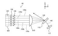
図1は本発明の第1実施形態にかかる光源装置の模式図である。本実施形態の光源装置10は、複数の光源モジュール100、第1透過型回折格子110及びセンサ112を備える。各光源モジュール100は、レーザ光源102、コリメートレンズ104、第2透過型回折格子106及びステージ108を含む。各光源モジュール100において、レーザ光源102、コリメートレンズ104及び第2透過型回折格子106が、同じステージ108に設けられ、モジュール全体を一体的に移動させることができる。この場合、レーザ光源102をステージ108に接するように設置して、ステージ108を冷却することによってレーザ光源102を冷却できるように設置することが好ましい。<First Embodiment>
FIG. 1 is a schematic diagram of a light source device according to a first embodiment of the present invention. The
図1において、説明の便宜のため、互いに直交するx軸、y軸及びz軸を表示している。なお、図1において、破線で概略的に光のビームを表す。破線で示した入射光120a、入射光120b及び入射光120cは、それぞれのレーザ光源102から出射され、コリメートレンズ104及び第2透過型回折格子106を通過して、第1透過型回折格子110に入射する。実際のビームは広がり角又は幅を持った光であるが、図1においては、説明の便宜上ビームの光軸のみを破線で示す。 In FIG. 1, for convenience of explanation, x-axis, y-axis, and z-axis orthogonal to each other are displayed. In FIG. 1, a broken line schematically represents a beam of light. The
図1に示すように、本実施形態においては、入射光120a、入射光120b及び入射光120cは、異なる入射角から第1透過型回折格子110に入射する。但し、本明細書において、いずれの入射光であるかを区別する必要がないとき、又は全ての入射光を指すとき、単に「入射光120」という場合もある。全ての入射光120の光軸が同じxz面上にある。 As shown in FIG. 1, in the present embodiment, the
レーザ光源102は、例えば350~550nmの間にピーク波長を有し、所定の利得スペクトル幅を有する光を出射するレーザダイオード(以下、「LD」ともいう)であってよい。例えば、レーザ光源102は、中心波長が410nmで、利得スペクトル幅Δλが20nmである光を出射する窒化物半導体を含むLDであってよい。この場合、レーザ光源102から出射する光の波長範囲は400~420nmである。 The
レーザ光源102となるLDの光出射側をフロント側、その反対側をリア側とした場合、フロント側には反射防止コーティングをして、反射率を0%近くまで、例えば0.1~2.0%程度まで低減したほうが好ましい。なお、リア側のミラーはほぼ100%、例えば85~99.9%の反射率を有することが好ましい。350~550nmの波長範囲の光を出射するLDは大気中では劣化しやすいため、レーザ光源102は、気密封止されていることが好ましい。例えば、レーザ光源102は、CAN型パッケージのLDであってよい。CAN型パッケージとすることにより、更に、冷却効果、静電気及び電磁波を遮蔽する効果を有する。また、350~550nmの波長範囲の光を出射するLDは窒化物半導体により形成することができる。 When the light emitting side of the LD to be the
コリメートレンズ104は、各レーザ光源102から出射された光をレーザ光源102の光軸に対して略平行光とする。各レーザ光源102に対応するコリメートレンズ104は、単一のレンズであってもよく、複数のレンズを組み合わせた組レンズであってもよい。 The
第2透過型回折格子106は、同一光源モジュール100におけるコリメートレンズ104から第1透過型回折格子110までの光路に配置される。第2透過型回折格子106は、同一光源モジュール100におけるレーザ光源102から出射された光の一部をレーザ光源102側へ回折して戻すことによって、レーザ光源102と第2透過型回折格子106との間で外部共振をさせる。より正確に言うと、レーザ光源102となるLDのリア側と第2透過型回折格子106との間で外部共振をさせる。すなわち、一組のレーザ光源102、コリメートレンズ104及び第2透過型回折格子106によって一つの外部共振器が形成される。当該外部共振器はリトロー型配置であってよい。リトロー型配置とは、回折角と入射角が同じになり、反射される回折光が入射光と同じルートを辿って光源にフィードバックされる配置をいう。 The second transmission
図2は図1に示した光源モジュール100の拡大模式図である。第2透過型回折格子106は、その格子溝方向が図1に示すy軸に平行になるように設置される。第2透過型回折格子106は、y軸に平行な回転軸202を有する。第2透過型回折格子106は、回転軸202を中心にステージ108に対して回転できる。第2透過型回折格子106は、回転軸202を中心に回転することによって、レーザ光源102に対する第2透過型回折格子106の配置角度を変化させる。この操作は、レーザ光源102から出射された光の、第2透過型回折格子への入射角を変更させることに対応する。それは、第2透過型回折格子106を透過して、第1透過型回折格子110に入射する入射光120の波長を選択(変更)することでもある。すなわち、第2透過型回折格子106は、外部共振器の波長選択素子である。 FIG. 2 is an enlarged schematic view of the
図2に示すように、光源モジュール100に素子駆動部204を設けて、第2透過型回折格子106の回転を制御してもよい。素子駆動部204として、例えばステッピングモータ等当該分野で公知の駆動手段を用いてよい。記述の便宜上、本明細書において、レーザ光源102から出射され第2透過型回折格子106を透過した光(入射光120)を光源モジュール100から出射された光又は外部共振器から出射された光ともいう。入射光120が第1透過型回折格子110に入射する入射角は、外部共振を実現する外部共振器の配置角度によって定められる。具体的には、第1透過型回折格子110に対する各光源モジュール100の位置および角度を設定することによって、入射光120の入射角を設定し調整することができる。 As shown in FIG. 2, the
第1透過型回折格子110は、その格子溝方向が図1に示すy軸に平行になるように設置される。第1透過型回折格子110は、各光源モジュール100のコリメートレンズ104及び第2透過型回折格子106を通過して異なる入射角から一領域に入射する入射光120a、入射光120b及び入射光120cを同じ回折角の方向に回折して合成し、反射回折光130を形成する。光源装置10は、複数の回折光を合成した反射回折光130を出力する。次に、第1透過型回折格子110における光の回折、反射、透過の状況について、図3を用いて説明する。 The first transmission
図3は第1透過型回折格子110における光の回折、反射、透過の状況を説明する説明図である。図3に示した一点鎖線は、第1透過型回折格子110の法線を示す。図3に示すように、各光源モジュール100から出射された入射光120a、入射光120b及び入射光120cが第1透過型回折格子110に入射すると、反射回折光130、透過回折光140、反射光330a、反射光330b、反射光330c、透過光340a、透過光340b、透過光340cなどが発生する。 FIG. 3 is an explanatory diagram illustrating the state of diffraction, reflection, and transmission of light in the first transmission
反射回折光130は、第1透過型回折格子110によって反射された1次回折光である。透過回折光140は、第1透過型回折格子110を透過した1次回折光である。反射光330a、反射光330b及び反射光330cは、第1透過型回折格子110によって反射された0次光であり、それぞれ入射光120a、入射光120b及び入射光120cに対応する。透過光340a、透過光340b及び透過光340cは、第1透過型回折格子110を透過した0次光であり、それぞれ入射光120a、入射光120b及び入射光120cに対応する。なお、2次以上の高次回折光もあるが、強度が非常に弱いので、図3において省略した。また、各入射光120a、120b、120cは第1透過型回折格子110を透過し、1次回折光を生じる際、厳密には重ならない。しかしながら、第1透過型回折格子110を透過した光は、それぞれ同じ回折角βで透過し、平行光となる。よって、図3において、透過回折光140は簡単のために1本の光軸で描写している。 The reflected diffracted light 130 is the primary diffracted light reflected by the first transmission
図3において、αa、αb及びαcはそれぞれ入射光120a、入射光120b及び入射光120cの入射角を表す。βは1次回折光の回折角を表す。反射回折光130、透過回折光140、反射光330a、反射光330b、反射光330c、透過光340a、透過光340b及び透過光340cの光軸も、入射光120a、入射光120b及び入射光120cの光軸と同じxz面上(図1参照)にある。 In FIG. 3, αa, αb, and αc represent the incident angles of the
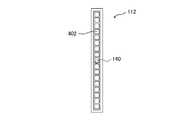
センサ112は、第1透過型回折格子110を透過した透過回折光140の位置を検知することによって、反射回折光130の位置ずれを検知する。センサ112は、受光素子から構成されてよい。当該受光素子の例として、例えばフォトダイオード、CMOS、CCDなどが挙げられる。特に、受光素子としてフォトダイオードを用いることが好ましい。フォトダイオードを利用することで、センサ112を安価に準備することができる。センサ112は、複数の受光素子から構成されてもよく、単体の受光素子から構成されてもよい。センサ112は、複数受光素子から構成された場合、回折光のずれた方向が判断しやすくなる。また、単体の受光素子から構成された場合、装置のコストを低減することができる。 The
図4は複数のフォトダイオードから構成されるリニアセンサの模式図である。図4に示すように、センサ112は、複数の受光素子が一列に並んだリニアセンサであってもよい。図4に示すセンサ112は、複数のフォトダイオード402が一列に並んで形成されている。センサ112を設置するとき、センサ112の受光面が透過回折光140に面して、予定する透過回折光140の光軸に垂直になるように配置し、複数のフォトダイオード402が並んだ方向(図4における縦方向)の中心軸が透過回折光140のあるxz面に載るように設置する(図1参照)。そうすると、図4に示すように、センサ112が透過回折光140を受光することができる。 FIG. 4 is a schematic diagram of a linear sensor composed of a plurality of photodiodes. As shown in FIG. 4, the
各入射光120の入射角が正しくなるようにレーザ光源を設置した場合、センサ112が所定の回折角に対応する位置で透過回折光140を検知することができる。全ての入射光120が同じ回折角に回折され、同軸に結合するので、Beam Parameter Product(BPP)が小さい反射回折光130が得られる。しかし、何れかの入射光120の入射角がずれると、透過回折光140がセンサ112に対して図4の上下方向に移動するかそのビームの形状が上下方向に広がるので、センサ112は透過回折光140のその位置ずれを検知することができる。入射光120の入射角がずれた場合、反射回折光130も透過回折光140と同様に位置ずれが発生するので、透過回折光140の位置ずれを検知することによって、反射回折光130の位置ずれも知ることができる。 When the laser light source is installed so that the incident angle of each
センサ112が第1透過型回折格子110の回折光の位置ずれを検知した場合、第2透過型回折格子106の角度を調整して第1透過型回折格子110に入射する光の波長を変更することによって、第1透過型回折格子110の回折光の位置ずれを補正することができる。以下、具体的な例をもって説明する。 When the
第1透過型回折格子110に入射する入射光120の入射角をαとし、第1透過型回折格子110によって回折される回折光の回折角をβとすると、数式1の関係を有する。 Assuming that the incident angle of the incident light 120 incident on the first transmission
[数1]
sinα + sinβ = N・m・λ
但し、Nは合波用回折格子である第1透過型回折格子110の1mmあたりの溝数、mは回折次数、λは光の波長をそれぞれ表す。[Number 1]
sinα + sinβ = N ・ m ・ λ
However, N represents the number of grooves per 1 mm of the first transmission
例えば、各レーザ光源102から中心波長が410nmであり波長範囲が400~420nmであるレーザビームを出射し、第1透過型回折格子110の1mmあたりの溝数が2222本であるとして、1次回折について考える。この場合、表1に示した波長λと入射角αの組み合わせにおいて同じ回折角βで回折され、結合した合成ビームが形成される。 For example, assuming that a laser beam having a central wavelength of 410 nm and a wavelength range of 400 to 420 nm is emitted from each

対して、上述したように、波長が414.63nmである入射光120aの所定の入射角は45.84度であるが、実際に対応する光源モジュール100を設置して得られた入射角が46.26度になったと仮定する。この場合、入射光120aの1次回折光の回折角βは、数式1を用いて計算すると、11.47度となり、所定の11.77度ではない。このままでは、第1透過型回折格子110によって合成した回折光(反射回折光130及び透過回折光140)は、同軸にならず、合成ビームのBPPが大きくなり、品質が低下する。しかしながら、上述したように、光源モジュール100そのものを精密に調整して、合波用回折格子である第1透過型回折格子110の一点にレーザ光を照射しながら、入射角αを適当な角度とすることは容易ではない。そのため、光源モジュール100の角度を調節して上記のような入射角のずれを補正することは難しいといえる。 On the other hand, as described above, the predetermined incident angle of the
一方で、本実施形態の光源装置10は、各光源モジュール100に波長選択素子となる第2透過型回折格子106を備えている。よって、センサ112で回折光のずれを検知した場合、第2透過型回折格子106の角度を各光源モジュール100に対して調整することができる。本実施形態の光源装置10の場合、第1透過型回折格子110に入射する入射角が46.26度になった入射光120aの波長を416.92nmに変更するだけで、入射光120aの回折光の回折角を11.47度から11.77度へと簡単に補正することができる。よって、位置調整が難しい光源モジュール100の位置設置ずれに対する許容度が大きくなる。 On the other hand, in the
他にも、本実施形態の光源装置10では、ビームアナライザやスペクトラムアナライザ等の高性能で高価な装置を用いる必要がないので、構造が簡単で、コストの上昇を抑えることができる。また、センサ112は、光源装置10に常備される。よって、光源装置10が出荷された後、何らかの原因で入射角がずれた場合にも、センサ112は回折光の位置ずれをすぐに検知することができる。 In addition, since it is not necessary to use a high-performance and expensive device such as a beam analyzer or a spectrum analyzer in the
第1透過型回折格子110は、その役割から、透過光が少なく、反射光が多いことが好ましい。それは、同じ透過型回折格子である第2透過型回折格子106と異なる。第1透過型回折格子110の0次光の透過率は、第2透過型回折格子106の0次光の透過率より低い。例えば、第1透過型回折格子110は、出力する反射回折光130(反射された1次回折光)の比率(1次回折光の反射率)が70~99%であってよく、好ましい範囲は85~99%である。透過回折光140(透過した1次回折光)の比率(1次回折光の透過率)が0.1~10%であってよく、好ましい範囲は0.1~5%である。透過した0次光の比率(0次光の透過率)が0.1~10%であってよく、好ましい範囲は0.1~5%である。例えば、第1透過型回折格子110として、1次回折光の反射率が97%、1次回折光の透過率が1%、0次光の透過率が1%である透過型回折格子を用いてよい。 Due to its role, the first transmission
第2透過型回折格子106は、透過光が多く、反射光が少ないことが好ましい。第2透過型回折格子106の0次光の透過率は、第1透過型回折格子110の0次光の透過率より高い。例えば、第2透過型回折格子106は、透過した0次光の比率(0次光の透過率)が60~90%であってよく、好ましい範囲は73~83%である。反射された1次回折光の比率(1次回折光の反射率)が10~30%であってよく、好ましい範囲は15~25%である。透過した1次回折光の比率(1次回折光の透過率)が0.1~5%であってよく、好ましい範囲は0.1~2%である。例えば、第2透過型回折格子106として、0次光の透過率が78%、1次回折光の反射率が20%、1次回折光の透過率が1%である透過型回折格子を用いてよい。 The second transmission
以上のように構成された実施形態の光源装置によれば、透過回折光をセンサで受光するとき、出力に寄与しない透過回折光の位置ずれを利用して、出力光の合波具合を評価することができる。よって、出力光の損失を抑制することができる。
また、位置ずれを検知する場合に、出力光を分岐する必要がないため、分岐のために必要な光学素子を挿入することがなく、ビーム品質の低下を抑制することができる。
また、合波用回折格子として、透過型回折格子を採用することで回折格子への光吸収を抑制し、回折格子の劣化を抑制することができる。反射型回折格子の場合は、光の入射面に金属膜が設けられており、光吸収が生じるので、劣化してしまう。According to the light source device of the embodiment configured as described above, when the transmitted diffracted light is received by the sensor, the combined wave condition of the output light is evaluated by utilizing the positional deviation of the transmitted diffracted light that does not contribute to the output. be able to. Therefore, the loss of output light can be suppressed.
Further, since it is not necessary to branch the output light when detecting the positional deviation, it is possible to suppress the deterioration of the beam quality without inserting the optical element necessary for the branching.
Further, by adopting a transmission type diffraction grating as the diffraction grating for combined waves, it is possible to suppress the absorption of light into the diffraction grating and suppress the deterioration of the diffraction grating. In the case of a reflective diffraction grating, a metal film is provided on the incident surface of light, and light absorption occurs, so that the grating deteriorates.
<第2実施形態>
図5は本発明の第2実施形態にかかる光源装置の模式図である。本実施形態の光源装置50は、第1実施形態の光源装置10の変形である。本実施形態において、第1実施形態と同じ機能を有する部品、部材、部分、素子、要素については、第1の実施形態と同じ符号を付しており、且つその説明を省略することがある。<Second Embodiment>
FIG. 5 is a schematic diagram of the light source device according to the second embodiment of the present invention. The
光源装置10に比して、光源装置50の主な相違は、センサ112がレーザ光源102に隣接して設けられ、第1透過型回折格子110を透過した透過回折光140がミラー502及びミラー504によって前記センサ112に導かれることである。 The main difference of the
図5に示すように、光源モジュール100には光源カバー512を設けることが好ましい。センサ112をレーザ光源102に隣接して設置すると、更に次のような効果が得られる。光源カバー512の一部を利用して、簡単にセンサカバー514を設けることができる。センサ112にセンサカバー514を設けると、周辺の光のノイズを遮断することができるので、センサ112の検知精度を高めることができる。なお、センサ112を第1透過型回折格子110の近くに設置すると、第1透過型回折格子110を透過した0次光などによる迷光の影響を受けやすいが、センサ112をレーザ光源102に隣接して設置すると、そのような影響を回避することができる。また、第1透過型回折格子110からセンサ112までの距離が長くなり、回折光のずれを顕著化する効果があり、検知精度を高めることができる。 As shown in FIG. 5, it is preferable that the
図6はセンサ112の前に集光レンズを設けた場合の説明図である。図6に示すように、センサ112に入射する光の光路に更に集光レンズ600を設けてもよい。この場合、センサ112は、集光レンズ600の後側焦点面に配置する。なお、集光レンズ600の光軸を透過回折光140の所望の光軸に合わせる。図6において、集光レンズ600の効果を説明するために、透過回折光140を一定の幅を有するビームとして表す。破線で表すように、透過回折光140は、透過回折光140a、140b、140c、140d及び140eを含むものとする。そのうち、透過回折光140a、140b及び140cは、透過回折光140の所望の光軸に平行する平行光であり、透過回折光140dと140eは、入射光120の入射角がずれたことによって回折角がずれた成分である。 FIG. 6 is an explanatory diagram when a condenser lens is provided in front of the
図6に示すように、透過回折光140の所望の光軸に平行する透過回折光140a、140b及び140cは、集光レンズ600によって1点に集光されるが、透過回折光140の所望の光軸に平行しない140dと140eは、同じ1点に集光できない。すなわち、集光レンズ600を設けることによって、透過回折光140の中から、ずれた回折光成分とずれていない回折光成分をより鮮明に分離することができるので、センサ112の検知精度をさらに高めることができる。 As shown in FIG. 6, the transmitted diffracted light 140a, 140b and 140c parallel to the desired optical axis of the transmitted diffracted light 140 are condensed to one point by the
<第3実施形態>
図7は本発明の第3実施形態にかかる光源装置の模式図である。本実施形態の光源装置80は、第1実施形態の光源装置10の変形である。本実施形態において、第1実施形態と同じ機能を有する部品、部材、部分、素子、要素については、第1の実施形態と同じ符号を付しており、且つその説明を省略することがある。
光源装置10に比して、光源装置80の主な相違は次のような点にある。レーザ光源102は、レーザダイオードバー802を構成したレーザダイオードである。レーザダイオードバー802は、同じ基板上に形成された複数(図7の例では5つ)のレーザダイオードがx軸方向に横一列に配列されて構成される。図7において、レーザダイオードであるレーザ光源102は、それに対応する導波路を表す破線によって示されている。なお、第2透過型回折格子106から第1透過型回折格子110までの光路に、偏向用集光レンズ810が配置されている。<Third Embodiment>
FIG. 7 is a schematic diagram of the light source device according to the third embodiment of the present invention. The
The main differences of the
第2透過型回折格子106を透過して、各外部共振器から出射された入射光120a、入射光120b、入射光120c、入射光120d及び入射光120eは、図7に示すz軸方向に偏向用集光レンズ810まで互いに平行に進行する。各入射光120が第1透過型回折格子110に入射する入射角は、偏向用集光レンズ810によって定められる。すなわち、各外部共振器から出射された入射光120は、偏向用集光レンズ810によって適切な入射角が付与され、第1透過型回折格子110に入射する。入射した光は第1透過型回折格子110によって同じ回折角に回折され結合して、反射回折光130と透過回折光140を形成する。 The
なお、本実施形態において、コリメートレンズ104として、レーザダイオードバー802のレーザダイオードに対応する複数のコリメートレンズが一体になっているレンズアレイを用いてもよい。複数のレーザ光源102を含むレーザダイオードバー802は、気密封止されることが好ましい。例えば、レーザダイオードバー802全体が気密封止されていてもよい。 In the present embodiment, as the
光源装置10と同じく、センサ112は透過回折光140の位置を検知する。したがって、本実施形態の光源装置80も、光源装置10と同様に、備えるセンサ112によって随時回折光の位置ずれ(回折角のずれ)を検知でき、なお、第2透過型回折格子106の角度を調整することによって、容易に回折光の位置ずれを補正することができる。 Like the
以上、実施形態を用いて本発明を説明したが、本発明の技術的範囲は上記実施形態の記載の範囲に限定されるものではない。上記実施の形態に、多様な変更または改良を加えることができることは当業者にとって明らかである。そのような変更または改良を加えた形態も本発明の技術的範囲に含まれ得ることは、特許請求の範囲の記載から明らかである。例えば、上記実施形態は本発明を分かりやすく説明するために詳細に説明したものであるが、本発明は必ずしも説明した全ての構成を備えるものに限定されるものではない。 Although the present invention has been described above using the embodiments, the technical scope of the present invention is not limited to the scope described in the above embodiments. It will be apparent to those skilled in the art that various changes or improvements can be made to the above embodiments. It is clear from the description of the claims that the form with such changes or improvements may be included in the technical scope of the present invention. For example, the above-described embodiment has been described in detail in order to explain the present invention in an easy-to-understand manner, but the present invention is not necessarily limited to those having all the described configurations.
なお、各実施形態の構成の一部について、他の構成によって置換することも可能であり、それを削除することも可能である。また、ある実施例の構成に他の実施例の構成を加えることも可能である。例えば、第1及び第3実施形態においても、第2実施形態のように、センサ112に入射する光の光路に更に集光レンズ600を設けてもよい。 It is possible to replace a part of the configuration of each embodiment with another configuration, and it is also possible to delete it. It is also possible to add the configuration of another embodiment to the configuration of one embodiment. For example, also in the first and third embodiments, as in the second embodiment, the
10、50、80 光源装置
100 光源モジュール
102 レーザ光源
104 コリメートレンズ
106 第2透過型回折格子
108 ステージ
110 第1透過型回折格子
112 センサ
120、120a、120b、120c、120d、120e 入射光
130 反射回折光
140、140a、140b、140c、140d、140e 透過回折光
202 回転軸
204 素子駆動部
330a、330b、330c 反射光
340a、340b、340c 透過光
402 フォトダイオード
502、504 ミラー
512 光源カバー
514 センサカバー
600 集光レンズ
802 レーザダイオードバー
810 偏向用集光レンズ10, 50, 80
Claims (10)
Translated fromJapanese前記第1の透過型回折格子によって合成した回折光の位置ずれを検知するセンサと、
前記コリメートレンズから前記第1の透過型回折格子までの光路に配置され、前記第1の透過型回折格子に入射する光の波長を選択する波長選択素子と、
を備え、
前記センサは、前記第1の透過型回折格子を透過した回折光を検知し、
前記第1の透過型回折格子によって反射された回折光が出力される
ことを特徴とする光源装置。It passes through a plurality of laser light sources that emit light having a predetermined gain spectrum width, a collimating lens that makes the light emitted from each of the laser light sources substantially parallel to the optical axis of the laser light source, and each of the collimating lenses. In a light source device including a first transmission type diffraction grating that diffracts and synthesizes light incident on one region from different incident angles in the direction of the same diffraction angle.
A sensor that detects the positional deviation of the diffracted light synthesized by the first transmission type diffraction grating, and
A wavelength selection element arranged in the optical path from the collimating lens to the first transmission type diffraction grating and selecting the wavelength of light incident on the first transmission type diffraction grating.
Equipped with
The sensor detects the diffracted light transmitted through the first transmission type diffraction grating, and detects the diffracted light.
A light source device characterized in that diffracted light reflected by the first transmission type diffraction grating is output.
前記センサが前記第1の透過型回折格子の回折光の位置ずれを検知した場合、前記波長選択素子の角度を調整して前記第1の透過型回折格子に入射する光の波長を変更することによって、前記第1の透過型回折格子の回折光の位置ずれを補正する
ことを特徴とする光源装置。In the light source device according to claim 1,
When the sensor detects the positional deviation of the diffracted light of the first transmission type diffraction grating, the wavelength of the light incident on the first transmission type diffraction grating is changed by adjusting the angle of the wavelength selection element. A light source device characterized by correcting the positional deviation of the diffracted light of the first transmission type diffraction grating.
前記センサは、前記レーザ光源に隣接して設けられ、
前記第1の透過型回折格子を透過した回折光は、ミラーによって前記センサに導かれる
ことを特徴とする光源装置。In the light source device according to claim 2,
The sensor is provided adjacent to the laser light source and is provided.
A light source device characterized in that the diffracted light transmitted through the first transmission type diffraction grating is guided to the sensor by a mirror.
前記波長選択素子は、第2の透過型回折格子であり、
前記第2の透過型回折格子の0次光の透過率が、前記第1の透過型回折格子の0次光の透過率より高く、
前記レーザ光源に対する当該第2の透過型回折格子の配置角度を変化させて、前記第1の透過型回折格子に入射する光の波長を変更する素子駆動部を備える
ことを特徴とする光源装置。In the light source device according to any one of claims 1 to 3.
The wavelength selection element is a second transmission type diffraction grating, and is
The transmittance of the 0th-order light of the second transmission type diffraction grating is higher than the transmittance of the 0th-order light of the first transmission type diffraction grating.
A light source device comprising an element driving unit that changes the arrangement angle of the second transmission type diffraction grating with respect to the laser light source to change the wavelength of light incident on the first transmission type diffraction grating.
前記センサは、複数の受光素子からなることを特徴とする光源装置。In the light source device according to any one of claims 1 to 4.
The sensor is a light source device including a plurality of light receiving elements.
前記センサは、受光素子が一列に並んだリニアセンサである
ことを特徴とする光源装置。In the light source device according to claim 5,
The sensor is a light source device characterized by being a linear sensor in which light receiving elements are arranged in a row.
前記センサは、単体の受光素子である
ことを特徴とする光源装置。In the light source device according to any one of claims 1 to 4.
The sensor is a light source device characterized by being a single light receiving element.
前記センサに入射する光の光路に集光レンズが設けられ、
前記センサは、前記集光レンズの後側焦点面に配置される
ことを特徴とする光源装置。In the light source device according to any one of claims 1 to 7.
A condenser lens is provided in the optical path of the light incident on the sensor.
The sensor is a light source device characterized in that it is arranged on the rear focal plane of the condenser lens.
前記レーザ光源は、窒化物半導体を含み、前記レーザ光源が気密封止されている
ことを特徴とする光源装置。In the light source device according to any one of claims 1 to 8.
The laser light source includes a nitride semiconductor, and the laser light source is airtightly sealed.
前記レーザ光源は、レーザダイオードバーを構成したレーザダイオードであり、
前記第1の透過型回折格子に入射する光の入射角は、前記波長選択素子から前記第1の透過型回折格子までの光路に配置された偏向用集光レンズによって定められる
ことを特徴とする光源装置。In the light source device according to any one of claims 1 to 9.
The laser light source is a laser diode constituting a laser diode bar.
The incident angle of the light incident on the first transmission type diffraction grating is characterized by being determined by a deflection condenser lens arranged in the optical path from the wavelength selection element to the first transmission type diffraction grating. Light source device.
Priority Applications (3)
| Application Number | Priority Date | Filing Date | Title |
|---|---|---|---|
| JP2018104572AJP7060799B2 (en) | 2018-05-31 | 2018-05-31 | Light source device |
| US16/427,184US10727648B2 (en) | 2018-05-31 | 2019-05-30 | Light source device |
| US16/904,886US10998698B2 (en) | 2018-05-31 | 2020-06-18 | Light source device |
Applications Claiming Priority (1)
| Application Number | Priority Date | Filing Date | Title |
|---|---|---|---|
| JP2018104572AJP7060799B2 (en) | 2018-05-31 | 2018-05-31 | Light source device |
Publications (2)
| Publication Number | Publication Date |
|---|---|
| JP2019212654A JP2019212654A (en) | 2019-12-12 |
| JP7060799B2true JP7060799B2 (en) | 2022-04-27 |
Family
ID=68692763
Family Applications (1)
| Application Number | Title | Priority Date | Filing Date |
|---|---|---|---|
| JP2018104572AActiveJP7060799B2 (en) | 2018-05-31 | 2018-05-31 | Light source device |
Country Status (2)
| Country | Link |
|---|---|
| US (2) | US10727648B2 (en) |
| JP (1) | JP7060799B2 (en) |
Families Citing this family (9)
| Publication number | Priority date | Publication date | Assignee | Title |
|---|---|---|---|---|
| WO2019224600A2 (en)* | 2018-05-22 | 2019-11-28 | Panasonic Intellectual Property Management Co. Ltd. | Power and spectral monitoring in wavelength beam combining laser systems |
| DE112019002638T5 (en)* | 2018-05-24 | 2021-03-11 | Panasonic Intellectual Property Management Co., Ltd. | REPLACEABLE LASER RESONATOR MODULES WITH ANGLE ADJUSTMENT |
| JP7060799B2 (en)* | 2018-05-31 | 2022-04-27 | 日亜化学工業株式会社 | Light source device |
| JP7212274B2 (en) | 2020-02-25 | 2023-01-25 | 日亜化学工業株式会社 | Light source device, direct diode laser device |
| KR102801486B1 (en)* | 2020-09-11 | 2025-04-25 | 삼성전자주식회사 | Optical inspection equipment |
| CN112241069A (en)* | 2020-10-15 | 2021-01-19 | 上海无线电设备研究所 | Optical fiber laser synthesis system |
| WO2023021675A1 (en)* | 2021-08-20 | 2023-02-23 | 三菱電機株式会社 | Semiconductor laser device and illumination device |
| CN115112610A (en)* | 2022-05-20 | 2022-09-27 | 中国科学院微电子研究所 | Optical measurement system |
| KR102744062B1 (en)* | 2022-10-12 | 2024-12-17 | 권도환 | Pulse laser selectively outputting signal of specific pulse width |
Citations (11)
| Publication number | Priority date | Publication date | Assignee | Title |
|---|---|---|---|---|
| JP2006286869A (en) | 2005-03-31 | 2006-10-19 | Fuji Photo Film Co Ltd | Fiber-module light source |
| JP2006352007A (en) | 2005-06-20 | 2006-12-28 | Sony Corp | Laser equipment |
| JP2007109923A (en) | 2005-10-14 | 2007-04-26 | Olympus Corp | Photodetector and optical communication system using same |
| JP2010122473A (en) | 2008-11-20 | 2010-06-03 | Ricoh Co Ltd | Light source device, optical scanning device, and image forming apparatus |
| JP2011035315A (en) | 2009-08-05 | 2011-02-17 | Sharp Corp | Light emitting element, light emitting device, and method of manufacturing light emitting element |
| JP2011237374A (en) | 2010-05-13 | 2011-11-24 | Seiko Epson Corp | Spectroscopic instrument, detector, and method for manufacturing spectroscopic instrument |
| JP2013007830A (en) | 2011-06-23 | 2013-01-10 | Seiko Epson Corp | Transmissive diffraction grating and detecting device |
| CN204156286U (en) | 2014-11-18 | 2015-02-11 | 中国工程物理研究院应用电子学研究所 | A kind of diode laser spectrum synthesizer based on double-grating external cavity feedback |
| WO2017075234A1 (en) | 2015-10-30 | 2017-05-04 | Seurat Technologies, Inc. | Additive manufacturing system and method |
| JP2017126619A (en) | 2016-01-12 | 2017-07-20 | 住友電気工業株式会社 | Optical module |
| WO2017134911A1 (en) | 2016-02-03 | 2017-08-10 | 古河電気工業株式会社 | Laser device |
Family Cites Families (9)
| Publication number | Priority date | Publication date | Assignee | Title |
|---|---|---|---|---|
| JPH067613B2 (en)* | 1985-07-02 | 1994-01-26 | 松下電器産業株式会社 | Frequency stabilized semiconductor laser device |
| US4847479A (en)* | 1988-06-06 | 1989-07-11 | Trw Inc. | System for controlling the wavelength and colinearity of multiplexed laser beams |
| JPH08204644A (en)* | 1995-01-25 | 1996-08-09 | Sony Corp | Optical space transmitter and its optical axis alignment method |
| US6907051B1 (en)* | 2001-08-31 | 2005-06-14 | Nlight Photonics Corporation | Dynamically spectrally tailored raman pump laser |
| JP4083464B2 (en) | 2002-05-02 | 2008-04-30 | 富士通株式会社 | Wavelength tunable light source device and optical amplifier using the same |
| JP5701618B2 (en) | 2010-03-04 | 2015-04-15 | ギガフォトン株式会社 | Extreme ultraviolet light generator |
| JP6122741B2 (en) | 2013-09-05 | 2017-04-26 | 本田技研工業株式会社 | Fastening structure of fiber reinforced resin frame |
| US20160344162A1 (en) | 2014-01-30 | 2016-11-24 | Mitsubishi Electric Corporation | Beam combining device and output recovery method for beam combining device |
| JP7060799B2 (en)* | 2018-05-31 | 2022-04-27 | 日亜化学工業株式会社 | Light source device |
- 2018
- 2018-05-31JPJP2018104572Apatent/JP7060799B2/enactiveActive
- 2019
- 2019-05-30USUS16/427,184patent/US10727648B2/enactiveActive
- 2020
- 2020-06-18USUS16/904,886patent/US10998698B2/enactiveActive
Patent Citations (11)
| Publication number | Priority date | Publication date | Assignee | Title |
|---|---|---|---|---|
| JP2006286869A (en) | 2005-03-31 | 2006-10-19 | Fuji Photo Film Co Ltd | Fiber-module light source |
| JP2006352007A (en) | 2005-06-20 | 2006-12-28 | Sony Corp | Laser equipment |
| JP2007109923A (en) | 2005-10-14 | 2007-04-26 | Olympus Corp | Photodetector and optical communication system using same |
| JP2010122473A (en) | 2008-11-20 | 2010-06-03 | Ricoh Co Ltd | Light source device, optical scanning device, and image forming apparatus |
| JP2011035315A (en) | 2009-08-05 | 2011-02-17 | Sharp Corp | Light emitting element, light emitting device, and method of manufacturing light emitting element |
| JP2011237374A (en) | 2010-05-13 | 2011-11-24 | Seiko Epson Corp | Spectroscopic instrument, detector, and method for manufacturing spectroscopic instrument |
| JP2013007830A (en) | 2011-06-23 | 2013-01-10 | Seiko Epson Corp | Transmissive diffraction grating and detecting device |
| CN204156286U (en) | 2014-11-18 | 2015-02-11 | 中国工程物理研究院应用电子学研究所 | A kind of diode laser spectrum synthesizer based on double-grating external cavity feedback |
| WO2017075234A1 (en) | 2015-10-30 | 2017-05-04 | Seurat Technologies, Inc. | Additive manufacturing system and method |
| JP2017126619A (en) | 2016-01-12 | 2017-07-20 | 住友電気工業株式会社 | Optical module |
| WO2017134911A1 (en) | 2016-02-03 | 2017-08-10 | 古河電気工業株式会社 | Laser device |
Also Published As
| Publication number | Publication date |
|---|---|
| JP2019212654A (en) | 2019-12-12 |
| US20190372311A1 (en) | 2019-12-05 |
| US20200321752A1 (en) | 2020-10-08 |
| US10727648B2 (en) | 2020-07-28 |
| US10998698B2 (en) | 2021-05-04 |
Similar Documents
| Publication | Publication Date | Title |
|---|---|---|
| JP7060799B2 (en) | Light source device | |
| JP7053993B2 (en) | Light source device | |
| JP4396868B2 (en) | Optical device using VIPA (virtual imaged phased array) for chromatic dispersion | |
| JP5911038B2 (en) | Semiconductor laser device | |
| US6608847B2 (en) | Tunable laser with suppression of spontaneous emission | |
| WO2016035349A1 (en) | Laser optical device and image projection device | |
| EP3855586B1 (en) | Laser device | |
| EP3355422B1 (en) | Wavelength tunable external cavity quantum cascade laser utilizing an angle tuned immersion grating as a wavelength selection filter element | |
| JP7323774B2 (en) | Light source device and external cavity laser module | |
| JP7280498B2 (en) | Light source device | |
| CN113615014B (en) | Semiconductor laser device | |
| JPH0763943A (en) | Multiplexer | |
| JP2016096333A (en) | Semiconductor laser device | |
| WO2018179858A1 (en) | Laser module and laser-emitting device | |
| US20220080525A1 (en) | Laser device and laser processing machine | |
| WO2021177001A1 (en) | Semiconductor laser device | |
| JP6518148B2 (en) | Optical module | |
| JP7456250B2 (en) | Light source equipment, projectors and machining equipment | |
| JP6822319B2 (en) | Wavelength Division Optical Transmission Module | |
| JP2008227170A (en) | Optical module | |
| US20140002827A1 (en) | None | |
| JP2025021691A (en) | Optical deflector and optical scanning device | |
| JP2008130977A (en) | Optical transmitting module and manufacturing method therefor | |
| WO2023021675A1 (en) | Semiconductor laser device and illumination device | |
| JP2011077076A (en) | External resonance type semiconductor laser |
Legal Events
| Date | Code | Title | Description |
|---|---|---|---|
| RD04 | Notification of resignation of power of attorney | Free format text:JAPANESE INTERMEDIATE CODE: A7424 Effective date:20190110 | |
| RD02 | Notification of acceptance of power of attorney | Free format text:JAPANESE INTERMEDIATE CODE: A7422 Effective date:20190117 | |
| A621 | Written request for application examination | Free format text:JAPANESE INTERMEDIATE CODE: A621 Effective date:20210508 | |
| A977 | Report on retrieval | Free format text:JAPANESE INTERMEDIATE CODE: A971007 Effective date:20220304 | |
| TRDD | Decision of grant or rejection written | ||
| A01 | Written decision to grant a patent or to grant a registration (utility model) | Free format text:JAPANESE INTERMEDIATE CODE: A01 Effective date:20220315 | |
| A61 | First payment of annual fees (during grant procedure) | Free format text:JAPANESE INTERMEDIATE CODE: A61 Effective date:20220328 | |
| R150 | Certificate of patent or registration of utility model | Ref document number:7060799 Country of ref document:JP Free format text:JAPANESE INTERMEDIATE CODE: R150 | |
| R250 | Receipt of annual fees | Free format text:JAPANESE INTERMEDIATE CODE: R250 |