JP7059423B2 - Semiconductor device - Google Patents
Semiconductor deviceDownload PDFInfo
- Publication number
- JP7059423B2 JP7059423B2JP2021072990AJP2021072990AJP7059423B2JP 7059423 B2JP7059423 B2JP 7059423B2JP 2021072990 AJP2021072990 AJP 2021072990AJP 2021072990 AJP2021072990 AJP 2021072990AJP 7059423 B2JP7059423 B2JP 7059423B2
- Authority
- JP
- Japan
- Prior art keywords
- oxide semiconductor
- transistor
- semiconductor layer
- electrode
- insulating layer
- Prior art date
- Legal status (The legal status is an assumption and is not a legal conclusion. Google has not performed a legal analysis and makes no representation as to the accuracy of the status listed.)
- Active
Links
Images


Classifications
- H—ELECTRICITY
- H10—SEMICONDUCTOR DEVICES; ELECTRIC SOLID-STATE DEVICES NOT OTHERWISE PROVIDED FOR
- H10D—INORGANIC ELECTRIC SEMICONDUCTOR DEVICES
- H10D30/00—Field-effect transistors [FET]
- H10D30/60—Insulated-gate field-effect transistors [IGFET]
- H10D30/67—Thin-film transistors [TFT]
- H10D30/674—Thin-film transistors [TFT] characterised by the active materials
- H10D30/6755—Oxide semiconductors, e.g. zinc oxide, copper aluminium oxide or cadmium stannate
- H—ELECTRICITY
- H01—ELECTRIC ELEMENTS
- H01L—SEMICONDUCTOR DEVICES NOT COVERED BY CLASS H10
- H01L21/00—Processes or apparatus adapted for the manufacture or treatment of semiconductor or solid state devices or of parts thereof
- H01L21/02—Manufacture or treatment of semiconductor devices or of parts thereof
- H01L21/04—Manufacture or treatment of semiconductor devices or of parts thereof the devices having potential barriers, e.g. a PN junction, depletion layer or carrier concentration layer
- H01L21/34—Manufacture or treatment of semiconductor devices or of parts thereof the devices having potential barriers, e.g. a PN junction, depletion layer or carrier concentration layer the devices having semiconductor bodies not provided for in groups H01L21/18, H10D48/04 and H10D48/07, with or without impurities, e.g. doping materials
- H01L21/38—Diffusion of impurity materials, e.g. doping materials, electrode materials, into or out of a semiconductor body, or between semiconductor regions
- H01L21/385—Diffusion of impurity materials, e.g. doping materials, electrode materials, into or out of a semiconductor body, or between semiconductor regions using diffusion into or out of a solid from or into a solid phase, e.g. a doped oxide layer
- H—ELECTRICITY
- H10—SEMICONDUCTOR DEVICES; ELECTRIC SOLID-STATE DEVICES NOT OTHERWISE PROVIDED FOR
- H10D—INORGANIC ELECTRIC SEMICONDUCTOR DEVICES
- H10D30/00—Field-effect transistors [FET]
- H10D30/60—Insulated-gate field-effect transistors [IGFET]
- H10D30/67—Thin-film transistors [TFT]
- H10D30/6729—Thin-film transistors [TFT] characterised by the electrodes
- H10D30/673—Thin-film transistors [TFT] characterised by the electrodes characterised by the shapes, relative sizes or dispositions of the gate electrodes
- H—ELECTRICITY
- H10—SEMICONDUCTOR DEVICES; ELECTRIC SOLID-STATE DEVICES NOT OTHERWISE PROVIDED FOR
- H10D—INORGANIC ELECTRIC SEMICONDUCTOR DEVICES
- H10D30/00—Field-effect transistors [FET]
- H10D30/60—Insulated-gate field-effect transistors [IGFET]
- H10D30/67—Thin-film transistors [TFT]
- H10D30/6757—Thin-film transistors [TFT] characterised by the structure of the channel, e.g. transverse or longitudinal shape or doping profile
- H—ELECTRICITY
- H10—SEMICONDUCTOR DEVICES; ELECTRIC SOLID-STATE DEVICES NOT OTHERWISE PROVIDED FOR
- H10D—INORGANIC ELECTRIC SEMICONDUCTOR DEVICES
- H10D62/00—Semiconductor bodies, or regions thereof, of devices having potential barriers
- H10D62/10—Shapes, relative sizes or dispositions of the regions of the semiconductor bodies; Shapes of the semiconductor bodies
- H10D62/124—Shapes, relative sizes or dispositions of the regions of semiconductor bodies or of junctions between the regions
- H10D62/125—Shapes of junctions between the regions
- H—ELECTRICITY
- H10—SEMICONDUCTOR DEVICES; ELECTRIC SOLID-STATE DEVICES NOT OTHERWISE PROVIDED FOR
- H10D—INORGANIC ELECTRIC SEMICONDUCTOR DEVICES
- H10D86/00—Integrated devices formed in or on insulating or conducting substrates, e.g. formed in silicon-on-insulator [SOI] substrates or on stainless steel or glass substrates
- H10D86/40—Integrated devices formed in or on insulating or conducting substrates, e.g. formed in silicon-on-insulator [SOI] substrates or on stainless steel or glass substrates characterised by multiple TFTs
- H10D86/421—Integrated devices formed in or on insulating or conducting substrates, e.g. formed in silicon-on-insulator [SOI] substrates or on stainless steel or glass substrates characterised by multiple TFTs having a particular composition, shape or crystalline structure of the active layer
- H10D86/423—Integrated devices formed in or on insulating or conducting substrates, e.g. formed in silicon-on-insulator [SOI] substrates or on stainless steel or glass substrates characterised by multiple TFTs having a particular composition, shape or crystalline structure of the active layer comprising semiconductor materials not belonging to the Group IV, e.g. InGaZnO
- H—ELECTRICITY
- H10—SEMICONDUCTOR DEVICES; ELECTRIC SOLID-STATE DEVICES NOT OTHERWISE PROVIDED FOR
- H10D—INORGANIC ELECTRIC SEMICONDUCTOR DEVICES
- H10D86/00—Integrated devices formed in or on insulating or conducting substrates, e.g. formed in silicon-on-insulator [SOI] substrates or on stainless steel or glass substrates
- H10D86/40—Integrated devices formed in or on insulating or conducting substrates, e.g. formed in silicon-on-insulator [SOI] substrates or on stainless steel or glass substrates characterised by multiple TFTs
- H10D86/60—Integrated devices formed in or on insulating or conducting substrates, e.g. formed in silicon-on-insulator [SOI] substrates or on stainless steel or glass substrates characterised by multiple TFTs wherein the TFTs are in active matrices
Landscapes
- Engineering & Computer Science (AREA)
- Physics & Mathematics (AREA)
- Condensed Matter Physics & Semiconductors (AREA)
- General Physics & Mathematics (AREA)
- Manufacturing & Machinery (AREA)
- Computer Hardware Design (AREA)
- Microelectronics & Electronic Packaging (AREA)
- Power Engineering (AREA)
- Thin Film Transistor (AREA)
- Solid State Image Pick-Up Elements (AREA)
- Metal-Oxide And Bipolar Metal-Oxide Semiconductor Integrated Circuits (AREA)
- Semiconductor Memories (AREA)
- Electroluminescent Light Sources (AREA)
- Internal Circuitry In Semiconductor Integrated Circuit Devices (AREA)
- Electrodes Of Semiconductors (AREA)
- Non-Volatile Memory (AREA)
Description
Translated fromJapanese本発明の一態様は、トランジスタおよび半導体装置、ならびにそれらの製造方法に関する
。One aspect of the present invention relates to transistors and semiconductor devices, and methods for manufacturing them.
なお、本発明の一態様は、上記の技術分野に限定されない。本明細書等で開示する発明の
一態様の技術分野は、物、方法、または、製造方法に関するものである。または、本発明
の一態様は、プロセス、マシン、マニュファクチャ、または、組成物(コンポジション・
オブ・マター)に関するものである。It should be noted that one aspect of the present invention is not limited to the above technical fields. The technical field of one aspect of the invention disclosed in the present specification and the like relates to a product, a method, or a manufacturing method. Alternatively, one aspect of the invention is a process, machine, manufacture, or composition (composition.
Of Matter).
なお、本明細書等において半導体装置とは、半導体特性を利用することで機能しうる装置
全般を指す。表示装置、液晶表示装置、発光装置、照明装置、電気光学装置、蓄電装置、
記憶装置、半導体回路、撮像装置および電子機器などは、半導体装置を有する場合がある
。In the present specification and the like, the semiconductor device refers to all devices that can function by utilizing the semiconductor characteristics. Display device, liquid crystal display device, light emitting device, lighting device, electro-optic device, power storage device,
Storage devices, semiconductor circuits, image pickup devices, electronic devices, and the like may have semiconductor devices.
近年は、酸化物半導体を用いたトランジスタが注目されている。酸化物半導体は、スパッ
タリング法などを用いて成膜できるため、大型の表示装置を構成するトランジスタの半導
体に用いることができる。また、酸化物半導体を用いたトランジスタは、非晶質シリコン
を用いたトランジスタの生産設備の一部を改良して利用することが可能であるため、設備
投資を抑えられるメリットもある。In recent years, transistors using oxide semiconductors have been attracting attention. Since the oxide semiconductor can be formed into a film by a sputtering method or the like, it can be used as a semiconductor of a transistor constituting a large display device. Further, a transistor using an oxide semiconductor can be used by improving a part of the production equipment of a transistor using amorphous silicon, so that there is an advantage that capital investment can be suppressed.
また、酸化物半導体を用いたトランジスタは、非導通状態において極めてリーク電流が小
さいことが知られている。例えば、酸化物半導体を用いたトランジスタの極めてリーク電
流が少ないという特性を応用した低消費電力のCPUなどが開示されている(特許文献1
参照。)。Further, it is known that a transistor using an oxide semiconductor has an extremely small leakage current in a non-conducting state. For example, a low power consumption CPU that applies the characteristic that the leakage current of a transistor using an oxide semiconductor is extremely small is disclosed (Patent Document 1).
reference. ).
電気特性の良好なトランジスタを提供することを課題の一とする。または、電気特性の安
定したトランジスタを提供することを課題の一とする。または、消費電力の少ないトラン
ジスタを提供することを課題の一とする。または、信頼性の良好なトランジスタを提供す
ることを課題の一とする。または、新規なトランジスタを提供することを課題の一とする
。または、これらのトランジスタの少なくとも一つを有する半導体装置を提供することを
課題の一とする。One of the challenges is to provide a transistor with good electrical characteristics. Alternatively, one of the problems is to provide a transistor having stable electrical characteristics. Alternatively, one of the challenges is to provide a transistor with low power consumption. Alternatively, one of the challenges is to provide a transistor with good reliability. Alternatively, one of the challenges is to provide a new transistor. Alternatively, one of the challenges is to provide a semiconductor device having at least one of these transistors.
なお、これらの課題の記載は、他の課題の存在を妨げるものではない。なお、本発明の一
態様は、これらの課題の全てを解決する必要はないものとする。なお、これら以外の課題
は、明細書、図面、請求項などの記載から、自ずと明らかとなるものであり、明細書、図
面、請求項などの記載から、これら以外の課題を抽出することが可能である。The description of these issues does not preclude the existence of other issues. It should be noted that one aspect of the present invention does not need to solve all of these problems. Issues other than these are self-evident from the description of the description, drawings, claims, etc., and it is possible to extract problems other than these from the description of the specification, drawings, claims, etc. Is.
本発明の一態様は、第1乃至第3の酸化物半導体層と、第1乃至第3の電極と、第1およ
び第2の絶縁層と、を有し、第1の酸化物半導体層は島状であり、かつ、第1の領域と、
第2の領域と、第3の領域と、を有し、第3の領域は、第1の領域と第2の領域に挟まれ
、第1の領域上に第1の電極を有し、第2の領域上に第2の電極を有し、第1の電極と第
2の電極上に、第2の酸化物半導体層を介して第1の絶縁層を有し、第2の酸化物半導体
層は第1の開口を有し、第1の絶縁層は第2の開口を有し、第1の開口と第2の開口は、
第3の領域と互いに重なり、第3の領域上に、第3の酸化物半導体層および第2の絶縁層
を介して第3の電極を有し、第1および第2の領域において、第2の酸化物半導体層は、
第1の酸化物半導体層の側面を覆い、第3の領域において、第3の酸化物半導体層は、第
1の酸化物半導体層の側面を覆うトランジスタである。なお、第3の領域は、平面におい
て、第1の領域と第2の領域に挟まれる。また、第2の酸化物半導体層は、第1の領域に
含まれる第1の側面と第2の領域に含まれる第2の側面を覆い、第3の酸化物半導体層は
、第3の領域に含まれる第3の側面を覆う。One aspect of the present invention includes a first to third oxide semiconductor layer, a first to third electrode, and first and second insulating layers, and the first oxide semiconductor layer is It is island-shaped and has a first area,
It has a second region and a third region, the third region is sandwiched between the first region and the second region, and has a first electrode on the first region and has a first electrode. A second electrode is provided on the
It overlaps with the third region and has a third electrode on the third region via the third oxide semiconductor layer and the second insulating layer, and in the first and second regions, the second Oxide semiconductor layer
The third oxide semiconductor layer is a transistor that covers the side surface of the first oxide semiconductor layer, and in the third region, the third oxide semiconductor layer covers the side surface of the first oxide semiconductor layer. The third region is sandwiched between the first region and the second region on a plane. Further, the second oxide semiconductor layer covers the first side surface included in the first region and the second side surface included in the second region, and the third oxide semiconductor layer covers the third region. Covers the third aspect contained in.
また、第3の電極の側面は第1の絶縁層に囲まれていることが好ましい。第2の酸化物半
導体層は、第1の酸化物半導体層の側面に接していることが好ましい。第3の酸化物半導
体層は、第1の酸化物半導体層の側面に接していることが好ましい。また、第1の酸化物
半導体層は、InまたはZnの一方、もしくは両方を含むことが好ましい。また、第2の
酸化物半導体層と第3の酸化物半導体層は、第1の酸化物半導体層に含まれる金属元素の
うち、少なくとも一種類の元素を含むことが好ましい。Further, it is preferable that the side surface of the third electrode is surrounded by the first insulating layer. The second oxide semiconductor layer is preferably in contact with the side surface of the first oxide semiconductor layer. The third oxide semiconductor layer is preferably in contact with the side surface of the first oxide semiconductor layer. Further, the first oxide semiconductor layer preferably contains one or both of In and Zn. Further, the second oxide semiconductor layer and the third oxide semiconductor layer preferably contain at least one kind of metal element contained in the first oxide semiconductor layer.
または、本発明の一態様は、上記トランジスタと、容量素子、または抵抗素子と、を有す
る半導体装置である。または、本発明の一態様は、該半導体装置と、アンテナ、バッテリ
、操作スイッチ、マイク、または、スピーカと、を有する電子機器である。または、本発
明の一態様は、上記トランジスタと、アンテナ、バッテリ、操作スイッチ、マイク、また
は、スピーカと、を有する電子機器である。Alternatively, one aspect of the present invention is a semiconductor device including the transistor and a capacitive element or a resistance element. Alternatively, one aspect of the present invention is an electronic device having the semiconductor device, an antenna, a battery, an operation switch, a microphone, or a speaker. Alternatively, one aspect of the present invention is an electronic device having the above-mentioned transistor and an antenna, a battery, an operation switch, a microphone, or a speaker.
電気特性の良好なトランジスタを提供することができる。または、電気特性の安定したト
ランジスタを提供することができる。または、消費電力の少ないトランジスタを提供する
ことができる。または、信頼性の良好なトランジスタを提供することができる。または、
新規なトランジスタを提供することができる。または、これらのトランジスタの少なくと
も一つを有する半導体装置を提供することができる。It is possible to provide a transistor having good electrical characteristics. Alternatively, it is possible to provide a transistor having stable electrical characteristics. Alternatively, it is possible to provide a transistor with low power consumption. Alternatively, it is possible to provide a transistor with good reliability. or,
A new transistor can be provided. Alternatively, a semiconductor device having at least one of these transistors can be provided.
なお、これらの効果の記載は、他の効果の存在を妨げるものではない。なお、本発明の一
態様は、これらの効果の全てを有する必要はない。なお、これら以外の効果は、明細書、
図面、請求項などの記載から、自ずと明らかとなるものであり、明細書、図面、請求項な
どの記載から、これら以外の効果を抽出することが可能である。The description of these effects does not preclude the existence of other effects. It should be noted that one aspect of the present invention does not have to have all of these effects. In addition, the effects other than these are described in the specification.
It is self-evident from the description of the drawings, claims, etc., and it is possible to extract effects other than these from the description of the specification, drawings, claims, etc.
実施の形態について、図面を用いて詳細に説明する。但し、本発明は以下の説明に限定さ
れず、本発明の趣旨及びその範囲から逸脱することなくその形態及び詳細を様々に変更し
得ることは当業者であれば容易に理解される。従って、本発明は以下に示す実施の形態の
記載内容に限定して解釈されるものではない。なお、以下に説明する発明の構成において
、同一部分又は同様な機能を有する部分には同一の符号を異なる図面間で共通して用い、
その繰り返しの説明は省略する場合がある。The embodiments will be described in detail with reference to the drawings. However, the present invention is not limited to the following description, and it is easily understood by those skilled in the art that the form and details of the present invention can be variously changed without departing from the spirit and scope of the present invention. Therefore, the present invention is not construed as being limited to the description of the embodiments shown below. In the configuration of the invention described below, the same reference numerals are commonly used between different drawings for the same parts or parts having similar functions.
The repeated description may be omitted.
また、図面などにおいて示す各構成の、位置、大きさ、範囲などは、発明の理解を容易と
するため、実際の位置、大きさ、範囲などを表していない場合がある。このため、開示す
る発明は、必ずしも、図面などに開示された位置、大きさ、範囲などに限定されない。例
えば、実際の製造工程において、エッチングなどの処理により層やレジストマスクなどが
意図せずに目減りすることがあるが、理解を容易とするために省略して示すことがある。In addition, the position, size, range, etc. of each configuration shown in the drawings may not represent the actual position, size, range, etc. in order to facilitate the understanding of the invention. Therefore, the disclosed invention is not necessarily limited to the position, size, range, etc. disclosed in the drawings and the like. For example, in an actual manufacturing process, layers, resist masks, and the like may be unintentionally reduced due to processing such as etching, but they may be omitted for ease of understanding.
また、特に上面図(「平面図」ともいう。)や斜視図などにおいて、発明の理解を容易と
するため、一部の構成要素の記載を省略する場合がある。また、一部の隠れ線などの記載
を省略する場合がある。Further, in order to facilitate understanding of the invention, in particular, in a top view (also referred to as a “plan view”) or a perspective view, the description of some components may be omitted. In addition, some hidden lines may be omitted.
本明細書等における「第1」、「第2」などの序数詞は、構成要素の混同を避けるために
付すものであり、工程順または積層順など、なんらかの順番や順位を示すものではない。
また、本明細書等において序数詞が付されていない用語であっても、構成要素の混同を避
けるため、特許請求の範囲において序数詞が付される場合がある。また、本明細書等にお
いて序数詞が付されている用語であっても、特許請求の範囲において異なる序数詞が付さ
れる場合がある。また、本明細書等において序数詞が付されている用語であっても、特許
請求の範囲などにおいて序数詞を省略する場合がある。The ordinal numbers such as "first" and "second" in the present specification and the like are attached to avoid confusion of the components, and do not indicate any order or order such as process order or stacking order.
In addition, even terms that do not have ordinal numbers in the present specification and the like may be given ordinal numbers within the scope of the claims in order to avoid confusion of the components. Further, even if the terms have ordinal numbers in the present specification and the like, different ordinal numbers may be added within the scope of the claims. Further, even if the terms have ordinal numbers in the present specification and the like, the ordinal numbers may be omitted in the scope of claims.
また、本明細書等において「電極」や「配線」の用語は、これらの構成要素を機能的に限
定するものではない。例えば、「電極」は「配線」の一部として用いられることがあり、
その逆もまた同様である。さらに、「電極」や「配線」の用語は、複数の「電極」や「配
線」が一体となって形成されている場合なども含む。Further, in the present specification and the like, the terms "electrode" and "wiring" do not functionally limit these components. For example, an "electrode" may be used as part of a "wiring",
The reverse is also true. Further, the terms "electrode" and "wiring" include the case where a plurality of "electrodes" and "wiring" are integrally formed.
なお、本明細書等において「上」や「下」の用語は、構成要素の位置関係が直上または直
下で、かつ、直接接していることを限定するものではない。例えば、「絶縁層A上の電極
B」の表現であれば、絶縁層Aの上に電極Bが直接接して形成されている必要はなく、絶
縁層Aと電極Bとの間に他の構成要素を含むものを除外しない。In the present specification and the like, the terms "upper" and "lower" do not limit the positional relationship of the components to be directly above or directly below and to be in direct contact with each other. For example, in the case of the expression "electrode B on the insulating layer A", it is not necessary that the electrode B is formed in direct contact with the insulating layer A, and another configuration is formed between the insulating layer A and the electrode B. Do not exclude those that contain elements.
また、ソースおよびドレインの機能は、異なる極性のトランジスタを採用する場合や、回
路動作において電流の方向が変化する場合など、動作条件などによって互いに入れ替わる
ため、いずれがソースまたはドレインであるかを限定することが困難である。このため、
本明細書においては、ソースおよびドレインの用語は、入れ替えて用いることができるも
のとする。In addition, the source and drain functions are interchanged depending on operating conditions, such as when transistors with different polarities are used or when the direction of current changes in circuit operation, so which one is the source or drain is limited. Is difficult. For this reason,
In the present specification, the terms source and drain may be used interchangeably.
また、本明細書等において、XとYとが接続されている、と明示的に記載されている場合
は、XとYとが電気的に接続されている場合と、XとYとが機能的に接続されている場合
と、XとYとが直接接続されている場合とが、本明細書等に開示されているものとする。
したがって、所定の接続関係、例えば、図または文章に示された接続関係に限定されず、
図または文章に示された接続関係以外のものも、図または文章に記載されているものとす
る。Further, in the present specification and the like, when it is explicitly stated that X and Y are connected, the case where X and Y are electrically connected and the case where X and Y function. It is assumed that the case where X and Y are directly connected and the case where X and Y are directly connected are disclosed in the present specification and the like.
Therefore, it is not limited to the predetermined connection relationship, for example, the connection relationship shown in the figure or text.
Other than the connection relationship shown in the figure or text, it shall be described in the figure or text.
また、本明細書等において、「電気的に接続」には、「何らかの電気的作用を有するもの
」を介して接続されている場合が含まれる。ここで、「何らかの電気的作用を有するもの
」は、接続対象間での電気信号の授受を可能とするものであれば、特に制限を受けない。
よって、「電気的に接続する」と表現される場合であっても、現実の回路においては、物
理的な接続部分がなく、配線が延在しているだけの場合もある。Further, in the present specification and the like, "electrically connected" includes the case of being connected via "something having some kind of electrical action". Here, the "thing having some kind of electrical action" is not particularly limited as long as it enables the exchange of electric signals between the connection targets.
Therefore, even when it is expressed as "electrically connected", in an actual circuit, there is a case where there is no physical connection portion and only the wiring is extended.
なお、チャネル長とは、例えば、トランジスタの上面図において、半導体(またはトラン
ジスタがオン状態のときに半導体の中で電流の流れる部分)とゲート電極とが互いに重な
る領域、またはチャネルが形成される領域における、ソース(ソース領域またはソース電
極)とドレイン(ドレイン領域またはドレイン電極)との間の距離をいう。なお、一つの
トランジスタにおいて、チャネル長が全ての領域で同じ値をとるとは限らない。即ち、一
つのトランジスタのチャネル長は、一つの値に定まらない場合がある。そのため、本明細
書では、チャネル長は、チャネルの形成される領域における、いずれか一の値、最大値、
最小値または平均値とする。The channel length is, for example, a region where a semiconductor (or a portion where a current flows in a semiconductor when the transistor is on) and a gate electrode overlap each other in a top view of a transistor, or a region where a channel is formed. In, the distance between the source (source region or source electrode) and the drain (drain region or drain electrode). In one transistor, the channel length does not always take the same value in all regions. That is, the channel length of one transistor may not be fixed to one value. Therefore, in the present specification, the channel length is any one value, the maximum value, in the region where the channel is formed.
The minimum or average value.
チャネル幅とは、例えば、半導体(またはトランジスタがオン状態のときに半導体の中で
電流の流れる部分)とゲート電極とが互いに重なる領域、またはチャネルが形成される領
域における、ソースとドレインとが向かい合っている部分の長さをいう。なお、一つのト
ランジスタにおいて、チャネル幅がすべての領域で同じ値をとるとは限らない。即ち、一
つのトランジスタのチャネル幅は、一つの値に定まらない場合がある。そのため、本明細
書では、チャネル幅は、チャネルの形成される領域における、いずれか一の値、最大値、
最小値または平均値とする。The channel width is, for example, the source and the drain facing each other in the region where the semiconductor (or the part where the current flows in the semiconductor when the transistor is on) and the gate electrode overlap each other, or the region where the channel is formed. The length of the part that is used. In one transistor, the channel width does not always take the same value in all regions. That is, the channel width of one transistor may not be fixed to one value. Therefore, in the present specification, the channel width is any one value, the maximum value, in the region where the channel is formed.
The minimum or average value.
なお、トランジスタの構造によっては、実際にチャネルの形成される領域におけるチャネ
ル幅(以下、「実効的なチャネル幅」ともいう。)と、トランジスタの上面図において示
されるチャネル幅(以下、「見かけ上のチャネル幅」ともいう。)と、が異なる場合があ
る。例えば、ゲート電極が半導体層の側面を覆う場合、実効的なチャネル幅が、見かけ上
のチャネル幅よりも大きくなり、その影響が無視できなくなる場合がある。例えば、微細
かつゲート電極が半導体層の側面を覆うトランジスタでは、半導体層の側面に形成される
チャネル領域の割合が大きくなる場合がある。その場合は、見かけ上のチャネル幅よりも
、実効的なチャネル幅の方が大きくなる。Depending on the structure of the transistor, the channel width in the region where the channel is actually formed (hereinafter, also referred to as “effective channel width”) and the channel width shown in the top view of the transistor (hereinafter, “apparently”). Also referred to as "channel width") and may be different. For example, when the gate electrode covers the side surface of the semiconductor layer, the effective channel width may be larger than the apparent channel width, and the influence thereof may not be negligible. For example, in a transistor that is fine and has a gate electrode covering the side surface of the semiconductor layer, the ratio of the channel region formed on the side surface of the semiconductor layer may be large. In that case, the effective channel width is larger than the apparent channel width.
このような場合、実効的なチャネル幅の、実測による見積もりが困難となる場合がある。
例えば、設計値から実効的なチャネル幅を見積もるためには、半導体の形状が既知という
仮定が必要である。したがって、半導体の形状が正確にわからない場合には、実効的なチ
ャネル幅を正確に測定することは困難である。In such a case, it may be difficult to estimate the effective channel width by actual measurement.
For example, in order to estimate the effective channel width from the design value, it is necessary to assume that the shape of the semiconductor is known. Therefore, if the shape of the semiconductor is not known accurately, it is difficult to accurately measure the effective channel width.
そこで、本明細書では、見かけ上のチャネル幅を、「囲い込みチャネル幅(SCW:Su
rrounded Channel Width)」と呼ぶ場合がある。また、本明細書
では、単にチャネル幅と記載した場合には、囲い込みチャネル幅または見かけ上のチャネ
ル幅を指す場合がある。または、本明細書では、単にチャネル幅と記載した場合には、実
効的なチャネル幅を指す場合がある。なお、チャネル長、チャネル幅、実効的なチャネル
幅、見かけ上のチャネル幅、囲い込みチャネル幅などは、断面TEM像などを解析するこ
となどによって、値を決定することができる。Therefore, in the present specification, the apparent channel width is referred to as “enclosure channel width (SCW: Su”).
It may be called "rounded Channel Withth)". Further, in the present specification, when simply described as a channel width, it may refer to an enclosed channel width or an apparent channel width. Alternatively, in the present specification, the term "channel width" may refer to an effective channel width. The values of the channel length, channel width, effective channel width, apparent channel width, enclosed channel width, and the like can be determined by analyzing a cross-sectional TEM image or the like.
なお、トランジスタの電界効果移動度や、チャネル幅当たりの電流値などを計算して求め
る場合、囲い込みチャネル幅を用いて計算する場合がある。その場合には、実効的なチャ
ネル幅を用いて計算する場合とは異なる値をとる場合がある。When calculating the electric field effect mobility of the transistor, the current value per channel width, or the like, the enclosed channel width may be used for calculation. In that case, the value may be different from the case calculated using the effective channel width.
なお、半導体の不純物とは、例えば、半導体を構成する主成分以外をいう。例えば、濃度
が0.1原子%未満の元素は不純物と言える。不純物が含まれることにより、例えば、半
導体のDOS(Density of State)が高くなることや、キャリア移動度
が低下することや、結晶性が低下することなどが起こる場合がある。半導体が酸化物半導
体である場合、半導体の特性を変化させる不純物としては、例えば、第1族元素、第2族
元素、第13族元素、第14族元素、第15族元素、および酸化物半導体の主成分以外の
遷移金属などがあり、特に、例えば、水素(水にも含まれる)、リチウム、ナトリウム、
シリコン、ホウ素、リン、炭素、窒素などがある。酸化物半導体の場合、例えば水素など
の不純物の混入によって酸素欠損を形成する場合がある。また、半導体がシリコンである
場合、半導体の特性を変化させる不純物としては、例えば、酸素、水素を除く第1族元素
、第2族元素、第13族元素、第15族元素などがある。The semiconductor impurities are, for example, other than the main components constituting the semiconductor. For example, an element having a concentration of less than 0.1 atomic% can be said to be an impurity. The inclusion of impurities may result in, for example, an increase in the DOS (Density of State) of the semiconductor, a decrease in carrier mobility, a decrease in crystallinity, and the like. When the semiconductor is an oxide semiconductor, the impurities that change the characteristics of the semiconductor include, for example,
There are silicon, boron, phosphorus, carbon, nitrogen and so on. In the case of oxide semiconductors, oxygen deficiency may be formed by mixing impurities such as hydrogen. When the semiconductor is silicon, the impurities that change the characteristics of the semiconductor include, for example,
また、本明細書において、「平行」とは、二つの直線が-10°以上10°以下の角度で
配置されている状態をいう。従って、-5°以上5°以下の場合も含まれる。また、「略
平行」とは、二つの直線が-30°以上30°以下の角度で配置されている状態をいう。
また、「垂直」および「直交」とは、二つの直線が80°以上100°以下の角度で配置
されている状態をいう。従って、85°以上95°以下の場合も含まれる。また、「略垂
直」とは、二つの直線が60°以上120°以下の角度で配置されている状態をいう。Further, in the present specification, "parallel" means a state in which two straight lines are arranged at an angle of −10 ° or more and 10 ° or less. Therefore, the case of −5 ° or more and 5 ° or less is also included. Further, "substantially parallel" means a state in which two straight lines are arranged at an angle of -30 ° or more and 30 ° or less.
Further, "vertical" and "orthogonal" mean a state in which two straight lines are arranged at an angle of 80 ° or more and 100 ° or less. Therefore, the case of 85 ° or more and 95 ° or less is also included. Further, "substantially vertical" means a state in which two straight lines are arranged at an angle of 60 ° or more and 120 ° or less.
なお、本明細書等において、計数値および計量値に関して「同一」、「同じ」、「等しい
」または「均一」(これらの同意語を含む)などと言う場合は、明示されている場合を除
き、プラスマイナス20%の誤差を含むものとする。In the present specification, etc., when the count value and the measured value are referred to as "same", "same", "equal" or "uniform" (including synonyms thereof), unless otherwise specified. , Plus or minus 20% error shall be included.
また、本明細書において、フォトリソグラフィ工程を行った後にエッチング工程を行う場
合は、特段の説明がない限り、フォトリソグラフィ工程で形成したレジストマスクは、エ
ッチング工程終了後に除去するものとする。Further, in the present specification, when the etching process is performed after the photolithography process is performed, the resist mask formed in the photolithography process is removed after the etching process is completed, unless otherwise specified.
また、本明細書等において、高電源電位VDD(以下、単に「VDD」または「H電位」
ともいう)とは、低電源電位VSSよりも高い電位の電源電位を示す。また、低電源電位
VSS(以下、単に「VSS」または「L電位」ともいう)とは、高電源電位VDDより
も低い電位の電源電位を示す。また、接地電位をVDDまたはVSSとして用いることも
できる。例えばVDDが接地電位の場合には、VSSは接地電位より低い電位であり、V
SSが接地電位の場合には、VDDは接地電位より高い電位である。Further, in the present specification and the like, the high power supply potential VDD (hereinafter, simply "VDD" or "H potential").
(Also referred to as) indicates a power supply potential having a potential higher than that of the low power supply potential VSS. Further, the low power supply potential VSS (hereinafter, also simply referred to as “VSS” or “L potential”) indicates a power supply potential having a potential lower than that of the high power supply potential VDD. The ground potential can also be used as VDD or VSS. For example, when VDD is the ground potential, VSS is a potential lower than the ground potential, and V
When SS is the ground potential, VDD is a potential higher than the ground potential.
なお、「膜」という言葉と、「層」という言葉とは、場合によっては、または、状況に応
じて、互いに入れ替えることが可能である。例えば、「導電層」という用語を、「導電膜
」という用語に変更することが可能な場合がある。または、例えば、「絶縁膜」という用
語を、「絶縁層」という用語に変更することが可能な場合がある。The word "membrane" and the word "layer" can be interchanged with each other in some cases or depending on the situation. For example, it may be possible to change the term "conductive layer" to the term "conductive film". Alternatively, for example, it may be possible to change the term "insulating film" to the term "insulating layer".
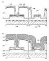
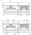
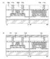
(実施の形態1)
本実施の形態では、本発明の一態様のトランジスタ100の構造および作製方法の一例に
ついて、図面を参照して説明する。(Embodiment 1)
In the present embodiment, an example of the structure and manufacturing method of the
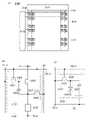
≪トランジスタ100の構造≫
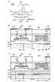
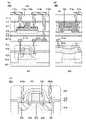
トランジスタ100の構造例について図面を用いて説明する。図1(A)は、トランジス
タ100の平面図である。また、図1(B)は、図1(A)にL1-L2の一点鎖線で示
す部位と、W1-W2の一点鎖線で示す部位の断面図である。図1(B)において、L1
-L2はトランジスタ100のチャネル長方向の断面図であり、W1-W2はトランジス
タ100のチャネル幅方向の断面図である。<< Structure of
A structural example of the
-L2 is a cross-sectional view of the
トランジスタ100は酸化物半導体層104、絶縁層108、電極109、電極105a
、および電極105bを有する。電極109はゲート電極として機能できる。絶縁層10
8はゲート絶縁層として機能できる。電極105aは、ソース電極またはドレイン電極の
一方として機能できる。電極105bは、ソース電極またはドレイン電極の他方として機
能できる。また、トランジスタ100は、基板101上に、絶縁層102および絶縁層1
03を介して設けられている。The
, And an
8 can function as a gate insulating layer. The
It is provided via 03.
図1(B)において、基板101上に絶縁層102が設けられ、絶縁層102上に絶縁層
103が設けられている。絶縁層103は凸部を有し、該凸部上に島状の酸化物半導体層
104aと島状の酸化物半導体層104bが設けられている。また、酸化物半導体層10
4b上に電極105a、および電極105bが設けられている。酸化物半導体層104b
の電極105aと重なる領域が、トランジスタ100のソースまたはドレインの一方とし
て機能できる。酸化物半導体層104bの電極105bと重なる領域が、トランジスタ1
00のソースまたはドレインの他方として機能できる。よって、酸化物半導体層104b
の、電極105aと電極105bに挟まれた領域121が、チャネル形成領域として機能
できる。In FIG. 1B, the insulating
An
The region overlapping the
Can act as either the source or drain of 00. Therefore, the
The
また、電極105a、および電極105b上に酸化物半導体層106が設けられ、酸化物
半導体層106上に絶縁層107が設けられている。また、酸化物半導体層106と絶縁
層107の領域121と重なる領域に開口が設けられ、該開口の側面および底面に沿って
酸化物半導体層104cが設けられている。また、該開口内に、酸化物半導体層104c
を介して、かつ、該開口の側面および底面に沿って、絶縁層108が設けられている。ま
た、該開口内に、酸化物半導体層104cおよび絶縁層108を介して、かつ、該開口の
側面および底面に沿って、電極109が設けられている。Further, the
An insulating
なお、該開口は、チャネル幅方向の断面において、酸化物半導体層104aおよび酸化物
半導体層104bよりも大きく設けられている。よって、領域121において、酸化物半
導体層104aおよび酸化物半導体層104bの側面は、酸化物半導体層104cに覆わ
れている。言い替えると、トランジスタのチャネル幅方向と交差する酸化物半導体層10
4aおよび酸化物半導体層104bの側面は、酸化物半導体層104cに覆われている。
領域121以外の酸化物半導体層104aおよび酸化物半導体層104bの側面は、酸化
物半導体層106に覆われている。言い替えると、トランジスタのチャネル長方向と交差
する酸化物半導体層104aおよび酸化物半導体層104bの側面は、酸化物半導体層1
06に覆われている。The opening is provided larger than the
The sides of 4a and the
The sides of the
It is covered with 06.
また、絶縁層107上に絶縁層110が設けられ、絶縁層110上に絶縁層111が設け
られている。また、絶縁層111上に電極113a、電極113b、および電極113c
が設けられている。電極113aは、絶縁層111、絶縁層110、絶縁層107、およ
び酸化物半導体層106の一部を除去して形成した開口において、コンタクトプラグ11
2aを介して電極105aと電気的に接続されている。また、電極113bは、絶縁層1
11、絶縁層110、絶縁層107、および酸化物半導体層106の一部を除去して形成
した開口において、コンタクトプラグ112bを介して電極105bと電気的に接続され
ている。また、電極113cは、絶縁層111および絶縁層110の一部を除去して形成
した開口において、コンタクトプラグ112cを介して電極109と電気的に接続されて
いる。Further, the insulating
Is provided. The
It is electrically connected to the
11. The opening formed by removing a part of the insulating
また、図1(B)に示すように、トランジスタ100は、チャネル幅方向において、電極
109が酸化物半導体層104bを覆っている。また、絶縁層103が凸部を有すること
によって、酸化物半導体層104bの側面も電極109で覆うことができる。すなわち、
電極109の電界によって、酸化物半導体層104bを電気的に取り囲むことができる構
造を有している(導電膜の電界によって、半導体を電気的に取り囲むトランジスタの構造
を、surrounded channel(s-channel)構造とよぶ。)。そ
のため、酸化物半導体層104bの全体(バルク)にチャネルを形成することもできる。
s-channel構造では、トランジスタのドレイン電流を大きくすることができ、さ
らに大きいオン電流(トランジスタがオン状態のときにソースとドレインの間に流れる電
流)を得ることができる。また、電極109の電界によって、酸化物半導体層104bに
形成されるチャネル形成領域の全領域を空乏化することができる。したがって、s-ch
annel構造では、トランジスタのオフ電流(トランジスタがオフ状態のときにソース
とドレインの間に流れる電流)をさらに小さくすることができる。なお、チャネル幅を小
さくすることで、s-channel構造によるオン電流の増大効果、オフ電流の低減効
果などを高めることができる。Further, as shown in FIG. 1B, in the
It has a structure that can electrically surround the
In the s-channel structure, the drain current of the transistor can be increased, and a larger on-current (current flowing between the source and the drain when the transistor is in the on state) can be obtained. Further, the electric field of the
In the annel structure, the off-current of the transistor (the current flowing between the source and the drain when the transistor is in the off state) can be further reduced. By reducing the channel width, the effect of increasing the on-current and the effect of reducing the off-current due to the s-channel structure can be enhanced.
〔酸化物半導体層104、酸化物半導体層106〕
酸化物半導体層104は、酸化物半導体層104a、酸化物半導体層104b、酸化物半
導体層104cを積層した構成を有する。[
The
酸化物半導体層104bは、例えば、インジウム(In)を含む酸化物である。酸化物半
導体層104bは、例えば、インジウムを含むと、キャリア移動度(電子移動度)が高く
なる。また、酸化物半導体層104bは、元素Mを含むと好ましい。The
元素Mは、好ましくは、アルミニウム、ガリウム、イットリウムまたはスズなどである。
そのほかの元素Mに適用可能な元素としては、ホウ素、シリコン、チタン、鉄、ニッケル
、ゲルマニウム、ジルコニウム、モリブデン、ランタン、セリウム、ネオジム、ハフニウ
ム、タンタル、タングステン、マグネシウムなどがある。ただし、元素Mとして、前述の
元素を複数組み合わせても構わない場合がある。元素Mは、例えば、酸素との結合エネル
ギーが高い元素である。元素Mは、例えば、酸化物のエネルギーギャップを大きくする機
能を有する元素である。また、酸化物半導体は、亜鉛を含むと好ましい。酸化物半導体は
亜鉛を含むと結晶化しやすくなる場合がある。The element M is preferably aluminum, gallium, yttrium, tin or the like.
Other elements applicable to the element M include boron, silicon, titanium, iron, nickel, germanium, zirconium, molybdenum, lanthanum, cerium, neodymium, hafnium, tantalum, tungsten, magnesium and the like. However, as the element M, a plurality of the above-mentioned elements may be combined in some cases. The element M is, for example, an element having a high binding energy with oxygen. The element M is, for example, an element having a function of increasing the energy gap of the oxide. Further, the oxide semiconductor preferably contains zinc. Oxide semiconductors may be easily crystallized if they contain zinc.
ただし、酸化物半導体層104bは、インジウムを含む酸化物に限定されない。酸化物半
導体層104bは、例えば、亜鉛スズ酸化物、ガリウムスズ酸化物、酸化ガリウムなどの
、インジウムを含まず、亜鉛を含む酸化物、ガリウムを含む酸化物、スズを含む酸化物な
どであっても構わない。However, the
酸化物半導体層104bは、例えば、エネルギーギャップが大きい酸化物を用いる。酸化
物半導体層104bのエネルギーギャップは、例えば、2.5eV以上4.2eV以下、
好ましくは2.8eV以上3.8eV以下、さらに好ましくは3eV以上3.5eV以下
とする。For the
It is preferably 2.8 eV or more and 3.8 eV or less, and more preferably 3 eV or more and 3.5 eV or less.
酸化物半導体層104は、スパッタリング法、CVD(Chemical Vapor
Deposition)法(MOCVD(Metal Organic Chemica
l Vapor Deposition)法、ALD(Atomic Layer De
position)法、熱CVD法またはPECVD(Plasma Enhanced
Chemical Vapor Deposition)法を含むがこれに限定されな
い)、MBE(Molecular Beam Epitaxy)法またはPLD(Pu
lsed Laser Deposition)法を用いて成膜するとよい。プラズマC
VD法は、比較的低温で高品質の膜が得られる。MOCVD法、ALD法、または熱CV
D法などの、成膜時にプラズマを用いない成膜方法を用いると、被形成面にダメージが生
じにくく、また、欠陥の少ない膜が得られる。The
Deposition) method (MOCVD (MetalOrganic Chemica)
l Vapor Deposition) method, ALD (Atomic Layer De)
position) method, thermal CVD method or PECVD (Plasma Enhanced)
Includes, but is not limited to, the Chemical Vapor Deposition) method), the MBE (Molecular Beam Epitaxy) method or the PLD (Pu).
It is advisable to form a film by using the lsed Laser Deposition) method. Plasma C
The VD method provides a high quality film at a relatively low temperature. MOCVD method, ALD method, or thermal CV
When a film forming method that does not use plasma at the time of film formation, such as the D method, is used, the surface to be formed is less likely to be damaged, and a film having few defects can be obtained.
例えば、酸化物半導体層104として、熱CVD法でInGaZnOX(X>0)膜を成
膜する場合には、トリメチルインジウム(In(CH3)3)、トリメチルガリウム(G
a(CH3)3)、およびジメチル亜鉛(Zn(CH3)2)を用いる。また、これらの
組み合わせに限定されず、トリメチルガリウムに代えてトリエチルガリウム(Ga(C2
H5)3)を用いることもでき、ジメチル亜鉛に代えてジエチル亜鉛(Zn(C2H5)
2)を用いることもできる。For example, when an InGaZnOX (X > 0) film is formed as the
a (CH3 )3 ) and dimethylzinc (Zn (CH3 )2 ) are used. Further, the combination thereof is not limited to triethylgallium (Ga (C2 )) instead of trimethylgallium.
H5 )3 ) can also be used, and instead of dimethylzinc, diethylzinc (Zn (C2 H5 )) can be used.
2 ) can also be used.
例えば、酸化物半導体層104として、ALD法で、In-Ga-Zn-O膜を成膜する
場合には、In(CH3)3ガスとO3ガスを順次繰り返し導入してIn-O層を形成し
、その後、Ga(CH3)3ガスとO3ガスを順次繰り返し導入してGaO層を形成し、
更にその後Zn(CH3)2ガスとO3ガスを順次繰り返し導入してZnO層を形成する
。なお、これらの層の順番はこの例に限らない。また、これらのガスを用いてIn-Ga
-O層やIn-Zn-O層、Ga-Zn-O層などの混合化合物層を形成しても良い。な
お、O3ガスに変えてAr等の不活性ガスで水をバブリングして得られたH2Oガスを用
いても良いが、Hを含まないO3ガスを用いる方が好ましい。また、In(CH3)3ガ
スにかえて、In(C2H5)3ガスやトリス(アセチルアセトナト)インジウムを用い
ても良い。なお、トリス(アセチルアセトナト)インジウムは、In(acac)3とも
呼ぶ。また、Ga(CH3)3ガスにかえて、Ga(C2H5)3ガスやトリス(アセチ
ルアセトナト)ガリウムを用いても良い。なお、トリス(アセチルアセトナト)ガリウム
は、Ga(acac)3とも呼ぶ。また、Zn(CH3)2ガスや、酢酸亜鉛を用いても
良い。これらのガス種には限定されない。For example, when an In—Ga—Zn—O film is formed as the
Further, after that, Zn (CH3 )2 gas and O3 gas are sequentially and repeatedly introduced to form a ZnO layer. The order of these layers is not limited to this example. In-Ga using these gases
A mixed compound layer such as an −O layer, an In—Zn—O layer, or a Ga—Zn—O layer may be formed. The H2 O gas obtained by bubbling water with an inert gas such as Ar may be used instead of the O3 gas, but it is preferable to use the O3 gas containing no H. Further, instead of In (CH3 )3 gas, In (C2 H5 )3 gas or tris (acetylacetonato) indium may be used. Indium tris (acetylacetonato) is also referred to as In (acac)3 . Further, Ga (C2 H5 )3 gas or tris (acetylacetonato) gallium may be used instead of Ga (CH3 )3 gas. In addition, tris (acetylacetonato) gallium is also referred to as Ga (acac)3 . Further, Zn (CH3 )2 gas or zinc acetate may be used. It is not limited to these gas species.
酸化物半導体層104をスパッタリング法で成膜する場合、パーティクル数低減のため、
インジウムを含むターゲットを用いると好ましい。また、元素Mの原子数比が高い酸化物
ターゲットを用いた場合、ターゲットの導電性が低くなる場合がある。インジウムを含む
ターゲットを用いる場合、ターゲットの導電率を高めることができ、DC放電、AC放電
が容易となるため、大面積の基板へ対応しやすくなる。したがって、半導体装置の生産性
を高めることができる。When the
It is preferable to use a target containing indium. Further, when an oxide target having a high atomic number ratio of the element M is used, the conductivity of the target may be low. When a target containing indium is used, the conductivity of the target can be increased, and DC discharge and AC discharge become easy, so that it becomes easy to cope with a large area substrate. Therefore, the productivity of the semiconductor device can be increased.
酸化物半導体層104をスパッタリング法で成膜する場合、ターゲットの原子数比は、I
n:M:Znが3:1:1、3:1:2、3:1:4、1:1:0.5、1:1:1、1
:1:2、1:4:4、4:2:4.1などとすればよい。When the
n: M: Zn is 3: 1: 1, 3: 1: 2, 3: 1: 4, 1: 1: 0.5, 1: 1: 1, 1
It may be 1: 2, 1: 4: 4, 4: 2: 4.1, or the like.
酸化物半導体層104をスパッタリング法で成膜する場合、ターゲットの原子数比からず
れた原子数比の膜が形成される場合がある。特に、亜鉛は、ターゲットの原子数比よりも
膜の原子数比が小さくなる場合がある。具体的には、ターゲットに含まれる亜鉛の原子数
比の40atomic%以上90atomic%程度以下となる場合がある。When the
酸化物半導体層104aおよび酸化物半導体層104cは、酸化物半導体層104bを構
成する酸素以外の元素のうち、1種類以上の同じ金属元素を含む材料により形成されるこ
とが好ましい。このような材料を用いると、酸化物半導体層104aおよび酸化物半導体
層104bとの界面、ならびに酸化物半導体層104cおよび酸化物半導体層104bと
の界面に界面準位を生じにくくすることができる。よって、界面におけるキャリアの散乱
や捕獲が生じにくく、トランジスタの電界効果移動度を向上させることが可能となる。ま
た、トランジスタのしきい値電圧(以下、「Vth」ともいう。)のばらつきを低減する
ことが可能となる。よって、良好な電気特性を有する半導体装置を実現することが可能と
なる。The
酸化物半導体層104aおよび酸化物半導体層104cの厚さは、3nm以上100nm
以下、好ましくは3nm以上50nm以下とする。また、酸化物半導体層104bの厚さ
は、3nm以上200nm以下、好ましくは3nm以上100nm以下、さらに好ましく
は3nm以上50nm以下とする。The thickness of the
Hereinafter, it is preferably 3 nm or more and 50 nm or less. The thickness of the
また、酸化物半導体層104bがIn-M-Zn酸化物(Inと元素MとZnを含む酸化
物)であり、酸化物半導体層104aおよび酸化物半導体層104cもIn-M-Zn酸
化物であるとき、酸化物半導体層104aおよび酸化物半導体層104cをIn:M:Z
n=x1:y1:z1[原子数比]、酸化物半導体層104bをIn:M:Zn=x2:
y2:z2[原子数比]とすると、y1/x1がy2/x2よりも大きくなる酸化物半導
体層104a、酸化物半導体層104c、および酸化物半導体層104bを選択する。好
ましくは、y1/x1がy2/x2よりも1.5倍以上大きくなる酸化物半導体層104
a、酸化物半導体層104c、および酸化物半導体層104bを選択する。さらに好まし
くは、y1/x1がy2/x2よりも2倍以上大きくなる酸化物半導体層104a、酸化
物半導体層104c、および酸化物半導体層104bを選択する。より好ましくは、y1
/x1がy2/x2よりも3倍以上大きくなる酸化物半導体層104a、酸化物半導体層
104cおよび酸化物半導体層104bを選択する。このとき、酸化物半導体層104b
において、y1がx1以上であるとトランジスタに安定した電気特性を付与できるため好
ましい。ただし、y1がx1の3倍以上になると、トランジスタの電界効果移動度が低下
してしまうため、y1はx1の3倍未満であると好ましい。酸化物半導体層104aおよ
び酸化物半導体層104cを上記構成とすることにより、酸化物半導体層104aおよび
酸化物半導体層104cを、酸化物半導体層104bよりも酸素欠損が生じにくい層とす
ることができる。Further, the
n = x1 : y1 : z1 [atomic number ratio], the
When y2 : z2 [atomic number ratio], the
a, the
Select the
In, it is preferable that y1 is x1 or more because stable electrical characteristics can be imparted to the transistor. However, when y1 becomes 3 times or more of x1 , the field effect mobility of the transistor decreases, so that y1 is preferably less than 3 times x1 . By having the
なお、酸化物半導体層104aがIn-M-Zn酸化物のとき、InおよびMの和を10
0atomic%としたとき、好ましくはInが50atomic%未満、Mが50at
omic%以上、さらに好ましくはInが25atomic%未満、Mが75atomi
c%以上とする。また、酸化物半導体層104bがIn-M-Zn酸化物のとき、Inお
よびMの和を100atomic%としたとき、好ましくはInが25atomic%以
上、Mが75atomic%未満、さらに好ましくはInが34atomic%以上、M
が66atomic%未満とする。また、酸化物半導体層104cがIn-M-Zn酸化
物のとき、InおよびMの和を100atomic%としたとき、好ましくはInが50
atomic%未満、Mが50atomic%以上、さらに好ましくはInが25ato
mic%未満、Mが75atomic%以上とする。なお、酸化物半導体層104cは、
酸化物半導体層104aと同種の酸化物を用いても構わない。When the
When it is set to 0 atomic%, In is preferably less than 50 atomic% and M is 50 at.
Omic% or more, more preferably In is less than 25 atomic%, M is 75 atomi
It should be c% or more. When the
Is less than 66 atomic%. Further, when the
Less than atomic%, M is 50 atomic% or more, more preferably In is 25 ato
It is less than mic% and M is 75 atomic% or more. The
An oxide of the same type as the
例えば、InまたはGaを含む酸化物半導体層104a、およびInまたはGaを含む酸
化物半導体層104cとして、In:Ga:Zn=1:3:2、1:3:4、1:3:6
、1:6:4、または1:9:6などの原子数比のターゲットを用いて形成したIn-G
a-Zn酸化物や、In:Ga=1:9、または7:93などの原子数比のターゲットを
用いて形成したIn-Ga酸化物を用いることができる。また、酸化物半導体層104b
として、例えば、In:Ga:Zn=1:1:1または3:1:2などの原子数比のター
ゲットを用いて形成したIn-Ga-Zn酸化物を用いることができる。なお、酸化物半
導体層104a、酸化物半導体層104b、および酸化物半導体層104cの原子数比は
それぞれ、誤差として上記の原子数比のプラスマイナス20%の変動を含む。For example, the
, 1: 6: 4, or 1: 9: 6, In-G formed using a target with an atomic number ratio, etc.
It is possible to use a—Zn oxide or In—Ga oxide formed by using a target having an atomic number ratio such as In: Ga = 1: 9, or 7:93. Further, the
As an example, an In—Ga—Zn oxide formed by using a target having an atomic number ratio such as In: Ga: Zn = 1: 1: 1 or 3: 1: 2 can be used. The atomic number ratios of the
酸化物半導体層104bは、酸化物半導体層104aおよび酸化物半導体層104cより
も電子親和力の大きい酸化物を用いる。例えば、酸化物半導体層104bとして、酸化物
半導体層104aおよび酸化物半導体層104cよりも電子親和力が0.07eV以上1
.3eV以下、好ましくは0.1eV以上0.7eV以下、さらに好ましくは0.15e
V以上0.4eV以下大きい酸化物を用いる。なお、電子親和力は、真空準位と伝導帯下
端のエネルギーとの差である。As the
.. 3 eV or less, preferably 0.1 eV or more and 0.7 eV or less, more preferably 0.15 e
Use an oxide larger than V or more and 0.4 eV or less. The electron affinity is the difference between the vacuum level and the energy at the lower end of the conduction band.
なお、インジウムガリウム酸化物は、小さい電子親和力と、高い酸素ブロック性を有する
。そのため、酸化物半導体層104cがインジウムガリウム酸化物を含むと好ましい。ガ
リウム原子割合[Ga/(In+Ga)]は、例えば、70%以上、好ましくは80%以
上、さらに好ましくは90%以上とする。Indium gallium oxide has a small electron affinity and a high oxygen blocking property. Therefore, it is preferable that the
ただし、酸化物半導体層104aまたは/および酸化物半導体層104cが、酸化ガリウ
ムであっても構わない。例えば、酸化物半導体層104cとして、酸化ガリウムを用いる
と電極105aまたは電極105bと電極109との間に生じるリーク電流を低減するこ
とができる。即ち、トランジスタ100のオフ電流を小さくすることができる。However, the
このとき、ゲート電圧を印加すると、酸化物半導体層104a、酸化物半導体層104b
、酸化物半導体層104cのうち、電子親和力の大きい酸化物半導体層104bにチャネ
ルが形成される。At this time, when a gate voltage is applied, the
Of the
酸化物半導体層を用いたトランジスタに安定した電気特性を付与するためには、酸化物半
導体層中の不純物及び酸素欠損を低減して高純度真性化し、少なくとも酸化物半導体層1
04bを真性または実質的に真性と見なせる酸化物半導体層とすることが好ましい。また
、少なくとも酸化物半導体層104b中のチャネル形成領域が真性または実質的に真性と
見なせる半導体層とすることが好ましい。In order to impart stable electrical characteristics to a transistor using an oxide semiconductor layer, impurities and oxygen deficiencies in the oxide semiconductor layer are reduced to achieve high purity authenticity, and at least the
It is preferable that 04b is an oxide semiconductor layer that can be regarded as genuine or substantially genuine. Further, it is preferable that at least the channel forming region in the
[酸化物半導体層のエネルギーバンド構造]
ここで、酸化物半導体層104a、酸化物半導体層104b、および酸化物半導体層10
4cの積層により構成される酸化物半導体層104の機能およびその効果について、図3
に示すエネルギーバンド構造図を用いて説明する。図3(A)は、図1(B)にA1-A
2の一点鎖線で示した部位のエネルギーバンド構造を示している。すなわち、図3(A)
は、トランジスタ100のチャネル形成領域のエネルギーバンド構造を示している。[Energy band structure of oxide semiconductor layer]
Here, the
FIG. 3 shows the functions and effects of the
This will be described with reference to the energy band structure diagram shown in. FIG. 3 (A) shows A1-A in FIG. 1 (B).
The energy band structure of the portion shown by the alternate long and short dash line of 2 is shown. That is, FIG. 3 (A)
Shows the energy band structure of the channel formation region of the
図3中、Ec382、Ec383a、Ec383b、Ec383c、Ec386は、それ
ぞれ、絶縁層103、酸化物半導体層104a、酸化物半導体層104b、酸化物半導体
層104c、絶縁層108の伝導帯下端のエネルギーを示している。In FIG. 3, Ec382, Ec383a, Ec383b, Ec383c, and Ec386 show the energies of the lower ends of the conduction bands of the insulating
ここで、電子親和力は、真空準位と価電子帯上端のエネルギーとの差(「イオン化ポテン
シャル」ともいう。)からエネルギーギャップを引いた値となる。なお、エネルギーギャ
ップは、分光エリプソメータ(HORIBA JOBIN YVON社 UT-300)
を用いて測定できる。また、真空準位と価電子帯上端のエネルギー差は、紫外線光電子分
光分析(UPS:Ultraviolet Photoelectron Spectr
oscopy)装置(PHI社 VersaProbe)を用いて測定できる。Here, the electron affinity is a value obtained by subtracting the energy gap from the difference between the vacuum level and the energy at the upper end of the valence band (also referred to as “ionization potential”). The energy gap is a spectroscopic ellipsometer (HORIBA JOBIN YVON UT-300).
Can be measured using. In addition, the energy difference between the vacuum level and the upper end of the valence band is determined by ultraviolet photoelectron spectroscopy (UPS).
It can be measured using an oscopy) device (PHI VersaProbe).
なお、原子数比がIn:Ga:Zn=1:3:2のターゲットを用いて形成したIn-G
a-Zn酸化物のエネルギーギャップは約3.5eV、電子親和力は約4.5eVである
。また、原子数比がIn:Ga:Zn=1:3:4のターゲットを用いて形成したIn-
Ga-Zn酸化物のエネルギーギャップは約3.4eV、電子親和力は約4.5eVであ
る。また、原子数比がIn:Ga:Zn=1:3:6のターゲットを用いて形成したIn
-Ga-Zn酸化物のエネルギーギャップは約3.3eV、電子親和力は約4.5eVで
ある。また、原子数比がIn:Ga:Zn=1:6:2のターゲットを用いて形成したI
n-Ga-Zn酸化物のエネルギーギャップは約3.9eV、電子親和力は約4.3eV
である。また、原子数比がIn:Ga:Zn=1:6:8のターゲットを用いて形成した
In-Ga-Zn酸化物のエネルギーギャップは約3.5eV、電子親和力は約4.4e
Vである。また、原子数比がIn:Ga:Zn=1:6:10のターゲットを用いて形成
したIn-Ga-Zn酸化物のエネルギーギャップは約3.5eV、電子親和力は約4.
5eVである。また、原子数比がIn:Ga:Zn=1:1:1のターゲットを用いて形
成したIn-Ga-Zn酸化物のエネルギーギャップは約3.2eV、電子親和力は約4
.7eVである。また、原子数比がIn:Ga:Zn=3:1:2のターゲットを用いて
形成したIn-Ga-Zn酸化物のエネルギーギャップは約2.8eV、電子親和力は約
5.0eVである。In—G formed by using a target having an atomic number ratio of In: Ga: Zn = 1: 3: 2.
The energy gap of the a-Zn oxide is about 3.5 eV, and the electron affinity is about 4.5 eV. Further, In-formed by using a target having an atomic number ratio of In: Ga: Zn = 1: 3: 4.
The energy gap of Ga—Zn oxide is about 3.4 eV, and the electron affinity is about 4.5 eV. In addition, In formed by using a target having an atomic number ratio of In: Ga: Zn = 1: 3: 6.
The energy gap of the -Ga-Zn oxide is about 3.3 eV, and the electron affinity is about 4.5 eV. Further, I formed by using a target having an atomic number ratio of In: Ga: Zn = 1: 6: 2.
The energy gap of n-Ga-Zn oxide is about 3.9 eV, and the electron affinity is about 4.3 eV.
Is. Further, the energy gap of the In—Ga—Zn oxide formed by using a target having an atomic number ratio of In: Ga: Zn = 1: 6: 8 is about 3.5 eV, and the electron affinity is about 4.4 e.
It is V. Further, the energy gap of the In—Ga—Zn oxide formed by using a target having an atomic number ratio of In: Ga: Zn = 1: 6: 10 is about 3.5 eV, and the electron affinity is about 4.
It is 5 eV. Further, the energy gap of the In—Ga—Zn oxide formed by using a target having an atomic number ratio of In: Ga: Zn = 1: 1: 1 is about 3.2 eV, and the electron affinity is about 4.
.. It is 7 eV. Further, the energy gap of the In—Ga—Zn oxide formed by using a target having an atomic number ratio of In: Ga: Zn = 3: 1: 2 is about 2.8 eV, and the electron affinity is about 5.0 eV.
絶縁層103と絶縁層108は絶縁物であるため、Ec382とEc386は、Ec38
3a、Ec383b、およびEc383cよりも真空準位に近い(電子親和力が小さい)
。Since the insulating
Closer to vacuum level than 3a, Ec383b, and Ec383c (small electron affinity)
..
また、Ec383aは、Ec383bよりも真空準位に近い。具体的には、Ec383a
は、Ec383bよりも0.07eV以上1.3eV以下、好ましくは0.1eV以上0
.7eV以下、さらに好ましくは0.15eV以上0.4eV以下真空準位に近いことが
好ましい。Further, Ec383a is closer to the vacuum level than Ec383b. Specifically, Ec383a
Is 0.07 eV or more and 1.3 eV or less, preferably 0.1 eV or more and 0, which is higher than Ec383b.
.. It is preferably 7 eV or less, more preferably 0.15 eV or more and 0.4 eV or less, close to the vacuum level.
また、Ec383cは、Ec383bよりも真空準位に近い。具体的には、Ec383c
は、Ec383bよりも0.07eV以上1.3eV以下、好ましくは0.1eV以上0
.7eV以下、さらに好ましくは0.15eV以上0.4eV以下真空準位に近いことが
好ましい。Further, Ec383c is closer to the vacuum level than Ec383b. Specifically, Ec383c
Is 0.07 eV or more and 1.3 eV or less, preferably 0.1 eV or more and 0, which is higher than Ec383b.
.. It is preferably 7 eV or less, more preferably 0.15 eV or more and 0.4 eV or less, close to the vacuum level.
ここで、酸化物半導体層104aと酸化物半導体層104bとの間には、酸化物半導体層
104aと酸化物半導体層104bとの混合領域を有する場合がある。また、酸化物半導
体層104bと酸化物半導体層104cとの間には、酸化物半導体層104bと酸化物半
導体層104cとの混合領域を有する場合がある。混合領域は、界面準位密度が低くなる
。そのため、酸化物半導体層104a、酸化物半導体層104bおよび酸化物半導体層1
04cの積層体は、それぞれの界面近傍において、エネルギーが連続的に変化する(連続
接合ともいう。)バンド構造となる。Here, between the
The laminated body of 04c has a band structure in which energy changes continuously (also referred to as continuous bonding) in the vicinity of each interface.
このとき、電子は、酸化物半導体層104a中および酸化物半導体層104c中ではなく
、酸化物半導体層104b中を主として移動する。したがって、酸化物半導体層104a
および酸化物半導体層104bの界面における界面準位密度、酸化物半導体層104bと
酸化物半導体層104cとの界面における界面準位密度を低くすることによって、酸化物
半導体層104b中で電子の移動が阻害されることが少なく、トランジスタ100のオン
電流を高くすることができる。At this time, the electrons mainly move in the
By lowering the interface state density at the interface of the
また、酸化物半導体層104aと絶縁層103の界面または界面近傍、および酸化物半導
体層104cと絶縁層108の界面または界面近傍には、不純物や欠陥に起因したトラッ
プ準位390が形成され得るものの、酸化物半導体層104a、および酸化物半導体層1
04cがあることにより、酸化物半導体層104bと当該トラップ準位とを遠ざけること
ができる。Further,
The presence of 04c makes it possible to keep the
なお、トランジスタ100がs-channel構造を有する場合、酸化物半導体層10
4bの全体にチャネルが形成される。したがって、酸化物半導体層104bが厚いほどチ
ャネル領域は大きくなる。即ち、酸化物半導体層104bが厚いほど、トランジスタ10
0のオン電流を高くすることができる。例えば、20nm以上、好ましくは40nm以上
、さらに好ましくは60nm以上、より好ましくは100nm以上の厚さの領域を有する
酸化物半導体層104bとすればよい。ただし、トランジスタ100を有する半導体装置
の生産性が低下する場合があるため、例えば、300nm以下、好ましくは200nm以
下、さらに好ましくは150nm以下の厚さの領域を有する酸化物半導体層104bとす
ればよい。When the
Channels are formed throughout 4b. Therefore, the thicker the
The on-current of 0 can be increased. For example, the
また、トランジスタ100のオン電流を高くするためには、酸化物半導体層104cの厚
さは小さいほど好ましい。例えば、10nm未満、好ましくは5nm以下、さらに好まし
くは3nm以下の領域を有する酸化物半導体層104cとすればよい。一方、酸化物半導
体層104cは、チャネルの形成される酸化物半導体層104bへ、隣接する絶縁体を構
成する酸素以外の元素(水素、シリコンなど)が入り込まないようブロックする機能を有
する。そのため、酸化物半導体層104cは、ある程度の厚さを有することが好ましい。
例えば、0.3nm以上、好ましくは1nm以上、さらに好ましくは2nm以上の厚さの
領域を有する酸化物半導体層104cとすればよい。また、酸化物半導体層104cは、
絶縁層103などから放出される酸素の外方拡散を抑制するために、酸素をブロックする
性質を有すると好ましい。Further, in order to increase the on-current of the
For example, the
In order to suppress the outward diffusion of oxygen released from the insulating
また、信頼性を高くするためには、酸化物半導体層104aは厚く、酸化物半導体層10
4cは薄いことが好ましい。例えば、10nm以上、好ましくは20nm以上、さらに好
ましくは40nm以上、より好ましくは60nm以上の厚さの領域を有する酸化物半導体
層104aとすればよい。酸化物半導体層104aの厚さを、厚くすることで、隣接する
絶縁体と酸化物半導体層104aとの界面からチャネルの形成される酸化物半導体層10
4bまでの距離を離すことができる。ただし、トランジスタ100を有する半導体装置の
生産性が低下する場合があるため、例えば、200nm以下、好ましくは120nm以下
、さらに好ましくは80nm以下の厚さの領域を有する酸化物半導体層104aとすれば
よい。Further, in order to increase the reliability, the
It is preferable that 4c is thin. For example, the
The distance up to 4b can be increased. However, since the productivity of the semiconductor device having the
なお、酸化物半導体中のシリコンは、キャリアトラップやキャリア発生源となる場合があ
る。したがって、酸化物半導体層104bのシリコン濃度は低いほど好ましい。例えば、
酸化物半導体層104bと酸化物半導体層104aとの間に、例えば、二次イオン質量分
析法(SIMS:Secondary Ion Mass Spectrometry)
において、1×10¹⁹atoms/cm3未満、好ましくは5×1018atoms/
cm3未満、さらに好ましくは2×10¹⁸atoms/cm3未満のシリコン濃度とな
る領域を有する。また、酸化物半導体層104bと酸化物半導体層104cとの間に、S
IMSにおいて、1×10¹⁹atoms/cm3未満、好ましくは5×1018ato
ms/cm3未満、さらに好ましくは2×1018atoms/cm3未満のシリコン濃
度となる領域を有する。Silicon in the oxide semiconductor may be a carrier trap or a carrier generation source. Therefore, the lower the silicon concentration of the
Between the
In, less than 1 × 10¹⁹ atoms / cm3 , preferably 5 × 10¹⁸ atoms / cm.
It has a region with a silicon concentration of less than cm3 , more preferably less than 2 × 10¹⁸ atoms / cm3 . Further, between the
In IMS, less than 1 × 10¹⁹ atoms / cm3 , preferably 5 × 10¹⁸ ato
It has a region with a silicon concentration of less than ms / cm3 , more preferably less than 2 × 10¹⁸ atoms / cm3 .
また、酸化物半導体層104bの水素濃度を低減するために、酸化物半導体層104aお
よび酸化物半導体層104cの水素濃度を低減すると好ましい。酸化物半導体層104a
および酸化物半導体層104cは、SIMSにおいて、2×10²⁰atoms/cm3
以下、好ましくは5×10¹⁹atoms/cm3以下、より好ましくは1×1019a
toms/cm3以下、さらに好ましくは5×1018atoms/cm3以下の水素濃
度となる領域を有する。また、酸化物半導体層104bの窒素濃度を低減するために、酸
化物半導体層104aおよび酸化物半導体層104cの窒素濃度を低減すると好ましい。
酸化物半導体層104aおよび酸化物半導体層104cは、SIMSにおいて、5×10
19atoms/cm3未満、好ましくは5×1018atoms/cm3以下、より好
ましくは1×10¹⁸atoms/cm3以下、さらに好ましくは5×1017atom
s/cm3以下の窒素濃度となる領域を有する。Further, in order to reduce the hydrogen concentration of the
And the
Hereinafter, preferably 5 × 10¹⁹ atoms / cm3 or less, more preferably 1 × 10¹⁹ a.
It has a region having a hydrogen concentration of toms / cm3 or less, more preferably 5 × 10¹⁸ atoms / cm3 or less. Further, in order to reduce the nitrogen concentration of the
The
19 atoms / cm less than3 , preferably 5 × 10¹⁸ atoms / cm3 or less, more preferably 1 × 10¹⁸ atoms / cm3 or less, still more preferably 5 × 10¹⁷ atoms.
It has a region with a nitrogen concentration of s / cm3 or less.
なお、酸化物半導体に銅が混入すると、電子トラップを生成する場合がある。電子トラッ
プは、トランジスタのしきい値電圧がプラス方向へ変動させる場合がある。したがって、
酸化物半導体層104bの表面または内部における銅濃度は低いほど好ましい。例えば、
酸化物半導体層104bは、銅濃度が1×10¹⁹atoms/cm3以下、5×101
8atoms/cm3以下、または1×1018atoms/cm3以下となる領域を有
すると好ましい。If copper is mixed in the oxide semiconductor, an electron trap may be generated. In the electronic trap, the threshold voltage of the transistor may fluctuate in the positive direction. therefore,
The lower the copper concentration on the surface or inside of the
The
It is preferable to have a region of8 atoms / cm3 or less, or 1 × 10¹⁸ atoms / cm3 or less.
上述の3層構造は一例である。例えば、酸化物半導体層104aまたは酸化物半導体層1
04cのない2層構造としても構わない。または、酸化物半導体層104aの上もしくは
下、または酸化物半導体層104c上もしくは下に、酸化物半導体層104a、酸化物半
導体層104bおよび酸化物半導体層104cとして例示した半導体のいずれか一を有す
る4層構造としても構わない。または、酸化物半導体層104aの上、酸化物半導体層1
04aの下、酸化物半導体層104cの上、酸化物半導体層104cの下のいずれか二箇
所以上に、酸化物半導体層104a、酸化物半導体層104bおよび酸化物半導体層10
4cとして例示した半導体のいずれか一を有するn層構造(nは5以上の整数)としても
構わない。The above-mentioned three-layer structure is an example. For example, the
A two-layer structure without 04c may be used. Alternatively, one of the semiconductors exemplified as the
The
It may have an n-layer structure (n is an integer of 5 or more) having any one of the semiconductors exemplified as 4c.
特に、本実施の形態に例示するトランジスタ100は、チャネル幅方向において、酸化物
半導体層104bの上面と側面が酸化物半導体層104cと接し、酸化物半導体層104
bの下面が酸化物半導体層104aと接して形成されている(図1(B)参照。)。この
ように、酸化物半導体層104bを酸化物半導体層104aと酸化物半導体層104cで
覆う構成とすることで、上記トラップ準位の影響をさらに低減することができる。In particular, in the
The lower surface of b is formed in contact with the
また、酸化物半導体層104a、および酸化物半導体層104cのバンドギャップは、酸
化物半導体層104bのバンドギャップよりも広いほうが好ましい。Further, it is preferable that the band gap of the
本発明の一態様によれば、電気特性のばらつきが少ないトランジスタを実現することがで
きる。よって、電気特性のばらつきが少ない半導体装置を実現することができる。本発明
の一態様によれば、信頼性の良好なトランジスタを実現することができる。よって、信頼
性の良好な半導体装置を実現することができる。According to one aspect of the present invention, it is possible to realize a transistor having little variation in electrical characteristics. Therefore, it is possible to realize a semiconductor device having little variation in electrical characteristics. According to one aspect of the present invention, a transistor with good reliability can be realized. Therefore, it is possible to realize a semiconductor device with good reliability.
また、酸化物半導体のバンドギャップは2eV以上あるため、チャネルが形成される半導
体層に酸化物半導体を用いたトランジスタは、オフ電流を極めて小さくすることができる
。具体的には、ソースとドレイン間の電圧が3.5V、室温(25℃)下において、チャ
ネル幅1μm当たりのオフ電流を1×10-20A未満、1×10-22A未満、あるい
は1×10-24A未満とすることができる。すなわち、オンオフ比を20桁以上150
桁以下とすることができる。Further, since the band gap of the oxide semiconductor is 2 eV or more, the transistor using the oxide semiconductor in the semiconductor layer on which the channel is formed can make the off-current extremely small. Specifically, when the voltage between the source and drain is 3.5 V and the room temperature (25 ° C) is normal, the off current per 1 μm of channel width is less than 1 ×10-20 A, 1 × 10-22A , or 1 It can be less than ×10-24A . That is, the on / off ratio is 20 digits or more and 150.
It can be less than or equal to a digit.
本発明の一態様によれば、消費電力が少ないトランジスタを実現することができる。よっ
て、消費電力が少ない半導体装置を実現することができる。According to one aspect of the present invention, a transistor with low power consumption can be realized. Therefore, it is possible to realize a semiconductor device with low power consumption.
なお、上述の3層構造は一例である。場合によっては、酸化物半導体層104aまたは酸
化物半導体層104cの一方を形成しない2層構造としても構わない。また、4層構造と
しても構わない。The above-mentioned three-layer structure is an example. In some cases, a two-layer structure may be used in which one of the
酸化物半導体層106は、酸化物半導体層104aまたは酸化物半導体層104cと同様
の材料を用いることができる。よって、酸化物半導体層104bと酸化物半導体層106
の間に混合領域を有する場合がある。また、酸化物半導体層106と絶縁層107の界面
または界面近傍には、不純物や欠陥に起因したトラップ準位が形成され得るものの、酸化
物半導体層106があることにより、酸化物半導体層104bと当該トラップ準位とを遠
ざけることができる。また、酸化物半導体層106として、Ga酸化物またはGa-Zn
酸化物(GaとZnを含む酸化物)を用いてもよい。As the
May have a mixed region between. Further, although trap levels due to impurities and defects may be formed at the interface between the
Oxides (oxides containing Ga and Zn) may be used.
[酸化物半導体の構造]
酸化物半導体は、単結晶酸化物半導体と、それ以外の非単結晶酸化物半導体とに分けられ
る。非単結晶酸化物半導体としては、CAAC-OS(C Axis Aligned
Crystalline Oxide Semiconductor)、多結晶酸化物半
導体、nc-OS(nanocrystalline Oxide Semicondu
ctor)、擬似非晶質酸化物半導体(a-like OS:amorphous li
ke Oxide Semiconductor)、非晶質酸化物半導体などがある。[Structure of oxide semiconductor]
Oxide semiconductors are divided into single crystal oxide semiconductors and other non-single crystal oxide semiconductors. As a non-single crystal oxide semiconductor, CAAC-OS (C Axis Aligned)
Crystalline Oxide Semiconductor), polycrystalline oxide semiconductor, nc-OS (nanocrystalline Oxide Semiconductor)
constructor), pseudo-amorphous oxide semiconductor (a-like OS: amorphous li)
There are ke Oxide Semiconductor), amorphous oxide semiconductors, and the like.
また別の観点では、酸化物半導体は、非晶質酸化物半導体と、それ以外の結晶性酸化物半
導体とに分けられる。結晶性酸化物半導体としては、単結晶酸化物半導体、CAAC-O
S、多結晶酸化物半導体、nc-OSなどがある。From another viewpoint, the oxide semiconductor is divided into an amorphous oxide semiconductor and other crystalline oxide semiconductors. Examples of the crystalline oxide semiconductor include a single crystal oxide semiconductor and CAAC-O.
There are S, polycrystalline oxide semiconductors, nc-OS and the like.
非晶質構造の定義としては、一般に、準安定状態で固定化していないこと、等方的であっ
て不均質構造を持たないことなどが知られている。また、結合角度が柔軟であり、短距離
秩序性は有するが、長距離秩序性を有さない構造と言い換えることもできる。As a definition of an amorphous structure, it is generally known that it is not immobilized in a metastable state, and that it is isotropic and does not have an anisotropic structure. In addition, it can be rephrased as a structure in which the coupling angle is flexible and the structure has short-range order but does not have long-range order.
逆の見方をすると、本質的に安定な酸化物半導体の場合、完全な非晶質(complet
ely amorphous)酸化物半導体と呼ぶことはできない。また、等方的でない
(例えば、微小な領域において周期構造を有する)酸化物半導体を、完全な非晶質酸化物
半導体と呼ぶことはできない。ただし、a-like OSは、微小な領域において周期
構造を有するものの、鬆(ボイドともいう。)を有し、不安定な構造である。そのため、
物性的には非晶質酸化物半導体に近いといえる。On the contrary, in the case of an essentially stable oxide semiconductor, it is completely amorphous.
It cannot be called an ely amorphous) oxide semiconductor. Further, an oxide semiconductor that is not isotropic (for example, having a periodic structure in a minute region) cannot be called a completely amorphous oxide semiconductor. However, although the a-like OS has a periodic structure in a minute region, it has a void (also referred to as a void) and has an unstable structure. for that reason,
It can be said that the physical characteristics are similar to those of amorphous oxide semiconductors.
<CAAC-OS>
まずは、CAAC-OSについて説明する。<CAAC-OS>
First, CAAC-OS will be described.
CAAC-OSは、c軸配向した複数の結晶部(ペレットともいう。)を有する酸化物半
導体の一つである。CAAC-OS is one of oxide semiconductors having a plurality of c-axis oriented crystal portions (also referred to as pellets).
透過型電子顕微鏡(TEM:Transmission Electron Micro
scope)によって、CAAC-OSの明視野像と回折パターンとの複合解析像(高分
解能TEM像ともいう。)を観察すると、複数のペレットを確認することができる。一方
、高分解能TEM像ではペレット同士の境界、即ち結晶粒界(グレインバウンダリーとも
いう。)を明確に確認することができない。そのため、CAAC-OSは、結晶粒界に起
因する電子移動度の低下が起こりにくいといえる。Transmission Electron Microscope (TEM: Transmission Electron Microscope)
By observing a composite analysis image (also referred to as a high-resolution TEM image) of the bright-field image of CAAC-OS and the diffraction pattern by scope), a plurality of pellets can be confirmed. On the other hand, in the high-resolution TEM image, the boundary between pellets, that is, the grain boundary (also referred to as grain boundary) cannot be clearly confirmed. Therefore, it can be said that CAAC-OS is unlikely to cause a decrease in electron mobility due to grain boundaries.
以下では、TEMによって観察したCAAC-OSについて説明する。図28(A)に、
試料面と略平行な方向から観察したCAAC-OSの断面の高分解能TEM像を示す。高
分解能TEM像の観察には、球面収差補正(Spherical Aberration
Corrector)機能を用いた。球面収差補正機能を用いた高分解能TEM像を、
特にCs補正高分解能TEM像と呼ぶ。Cs補正高分解能TEM像の取得は、例えば、日
本電子株式会社製原子分解能分析電子顕微鏡JEM-ARM200Fなどによって行うこ
とができる。The CAAC-OS observed by TEM will be described below. In FIG. 28 (A),
A high-resolution TEM image of a cross section of CAAC-OS observed from a direction substantially parallel to the sample surface is shown. For observation of high-resolution TEM images, spherical aberration correction (Spherical Aberration)
The Director) function was used. A high-resolution TEM image using the spherical aberration correction function,
In particular, it is called a Cs-corrected high-resolution TEM image. The acquisition of the Cs-corrected high-resolution TEM image can be performed by, for example, the atomic resolution analysis electron microscope JEM-ARM200F manufactured by JEOL Ltd.
図28(A)の領域(1)を拡大したCs補正高分解能TEM像を図28(B)に示す。
図28(B)より、ペレットにおいて、金属原子が層状に配列していることを確認できる
。金属原子の各層の配列は、CAAC-OSの膜を形成する面(被形成面ともいう。)ま
たは上面の凹凸を反映しており、CAAC-OSの被形成面または上面と平行となる。FIG. 28 (B) shows a Cs-corrected high-resolution TEM image in which the region (1) of FIG. 28 (A) is enlarged.
From FIG. 28B, it can be confirmed that the metal atoms are arranged in layers in the pellet. The arrangement of each layer of the metal atom reflects the unevenness of the surface (also referred to as the formed surface) or the upper surface of the CAAC-OS film, and is parallel to the formed surface or the upper surface of the CAAC-OS.
図28(B)に示すように、CAAC-OSは特徴的な原子配列を有する。図28(C)
は、特徴的な原子配列を、補助線で示したものである。図28(B)および図28(C)
より、ペレット一つの大きさは1nm以上のものや、3nm以上のものがあり、ペレット
とペレットとの傾きにより生じる隙間の大きさは0.8nm程度であることがわかる。し
たがって、ペレットを、ナノ結晶(nc:nanocrystal)と呼ぶこともできる
。また、CAAC-OSを、CANC(C-Axis Aligned nanocry
stals)を有する酸化物半導体と呼ぶこともできる。As shown in FIG. 28 (B), CAAC-OS has a characteristic atomic arrangement. FIG. 28 (C)
Shows the characteristic atomic arrangement with auxiliary lines. 28 (B) and 28 (C)
From this, it can be seen that the size of one pellet is 1 nm or more and 3 nm or more, and the size of the gap generated by the inclination between the pellet and the pellet is about 0.8 nm. Therefore, the pellets can also be referred to as nanocrystals (nc: nanocrystals). In addition, CAAC-OS can be used as CANC (C-Axis Aligned nanocry).
It can also be called an oxide semiconductor having stals).
ここで、Cs補正高分解能TEM像をもとに、基板5120上のCAAC-OSのペレッ
ト5100の配置を模式的に示すと、レンガまたはブロックが積み重なったような構造と
なる(図28(D)参照。)。図28(C)で観察されたペレットとペレットとの間で傾
きが生じている箇所は、図28(D)に示す領域5161に相当する。Here, if the arrangement of the CAAC-
また、図29(A)に、試料面と略垂直な方向から観察したCAAC-OSの平面のCs
補正高分解能TEM像を示す。図29(A)の領域(1)、領域(2)および領域(3)
を拡大したCs補正高分解能TEM像を、それぞれ図29(B)、図29(C)および図
29(D)に示す。図29(B)、図29(C)および図29(D)より、ペレットは、
金属原子が三角形状、四角形状または六角形状に配列していることを確認できる。しかし
ながら、異なるペレット間で、金属原子の配列に規則性は見られない。Further, in FIG. 29 (A), Cs on the plane of CAAC-OS observed from a direction substantially perpendicular to the sample surface.
A corrected high resolution TEM image is shown. Area (1), area (2) and area (3) of FIG. 29 (A)
The enlarged Cs-corrected high-resolution TEM images are shown in FIGS. 29 (B), 29 (C), and 29 (D), respectively. From FIGS. 29 (B), 29 (C) and 29 (D), the pellets are:
It can be confirmed that the metal atoms are arranged in a triangular shape, a square shape, or a hexagonal shape. However, there is no regularity in the arrangement of metal atoms between different pellets.
次に、X線回折(XRD:X-Ray Diffraction)によって解析したCA
AC-OSについて説明する。例えば、InGaZnO4の結晶を有するCAAC-OS
に対し、out-of-plane法による構造解析を行うと、図30(A)に示すよう
に回折角(2θ)が31°近傍にピークが現れる場合がある。このピークは、InGaZ
nO4の結晶の(009)面に帰属されることから、CAAC-OSの結晶がc軸配向性
を有し、c軸が被形成面または上面に略垂直な方向を向いていることが確認できる。Next, CA analyzed by X-ray diffraction (XRD: X-Ray Diffraction).
The AC-OS will be described. For example, CAAC-OS having crystals of InGaZnO4 .
On the other hand, when the structural analysis by the out-of-plane method is performed, a peak may appear in the vicinity of the diffraction angle (2θ) of 31 ° as shown in FIG. 30A. This peak is InGaZ
Since it belongs to the (009) plane of the crystal ofno4 , it is confirmed that the crystal of CAAC-OS has c-axis orientation and the c-axis is oriented substantially perpendicular to the surface to be formed or the upper surface. can.
なお、CAAC-OSのout-of-plane法による構造解析では、2θが31°
近傍のピークの他に、2θが36°近傍にもピークが現れる場合がある。2θが36°近
傍のピークは、CAAC-OS中の一部に、c軸配向性を有さない結晶が含まれることを
示している。より好ましいCAAC-OSは、out-of-plane法による構造解
析では、2θが31°近傍にピークを示し、2θが36°近傍にピークを示さない。In the structural analysis of CAAC-OS by the out-of-plane method, 2θ is 31 °.
In addition to the peaks in the vicinity, peaks may appear in the vicinity of 2θ of 36 °. The peak in which 2θ is in the vicinity of 36 ° indicates that a part of CAAC-OS contains crystals having no c-axis orientation. In a more preferable CAAC-OS, in the structural analysis by the out-of-plane method, 2θ shows a peak near 31 ° and 2θ does not show a peak near 36 °.
一方、CAAC-OSに対し、c軸に略垂直な方向からX線を入射させるin-plan
e法による構造解析を行うと、2θが56°近傍にピークが現れる。このピークは、In
GaZnO4の結晶の(110)面に帰属される。CAAC-OSの場合は、2θを56
°近傍に固定し、試料面の法線ベクトルを軸(φ軸)として試料を回転させながら分析(
φスキャン)を行っても、図30(B)に示すように明瞭なピークは現れない。これに対
し、InGaZnO4の単結晶酸化物半導体であれば、2θを56°近傍に固定してφス
キャンした場合、図30(C)に示すように(110)面と等価な結晶面に帰属されるピ
ークが6本観察される。したがって、XRDを用いた構造解析から、CAAC-OSは、
a軸およびb軸の配向が不規則であることが確認できる。On the other hand, in-plan in which X-rays are incident on CAAC-OS from a direction substantially perpendicular to the c-axis.
When the structural analysis by the e method is performed, a peak appears in the vicinity of 2θ at 56 °. This peak is In
It is attributed to the (110) plane of the crystal of GaZnO4 . In the case of CAAC-OS, 2θ is 56
It is fixed in the vicinity of ° and analyzed while rotating the sample with the normal vector of the sample surface as the axis (φ axis).
Even if φ scan) is performed, no clear peak appears as shown in FIG. 30 (B). On the other hand, in the case of the single crystal oxide semiconductor of InGaZnO4 , when 2θ is fixed in the vicinity of 56 ° and φ-scanned, it belongs to the crystal plane equivalent to the (110) plane as shown in FIG. 30 (C). Six peaks are observed. Therefore, from the structural analysis using XRD, CAAC-OS is
It can be confirmed that the orientation of the a-axis and the b-axis is irregular.
次に、電子回折によって解析したCAAC-OSについて説明する。例えば、InGaZ
nO4の結晶を有するCAAC-OSに対し、試料面に平行にプローブ径が300nmの
電子線を入射させると、図31(A)に示すような回折パターン(制限視野透過電子回折
パターンともいう。)が現れる場合がある。この回折パターンには、InGaZnO4の
結晶の(009)面に起因するスポットが含まれる。したがって、電子回折によっても、
CAAC-OSに含まれるペレットがc軸配向性を有し、c軸が被形成面または上面に略
垂直な方向を向いていることがわかる。一方、同じ試料に対し、試料面に垂直にプローブ
径が300nmの電子線を入射させたときの回折パターンを図31(B)に示す。図31
(B)より、リング状の回折パターンが確認される。したがって、電子回折によっても、
CAAC-OSに含まれるペレットのa軸およびb軸は配向性を有さないことがわかる。
なお、図31(B)における第1リングは、InGaZnO4の結晶の(010)面およ
び(100)面などに起因すると考えられる。また、図31(B)における第2リングは
(110)面などに起因すると考えられる。Next, the CAAC-OS analyzed by electron diffraction will be described. For example, InGaZ
When an electron beam having a probe diameter of 300 nm is incident on CAAC-OS having a crystal of nO4 in parallel with the sample surface, it is also referred to as a diffraction pattern (also referred to as a limited field transmission electron diffraction pattern) as shown in FIG. 31 (A). ) May appear. This diffraction pattern includes spots due to the (009) plane of the crystal of InGaZnO4 . Therefore, even by electron diffraction,
It can be seen that the pellets contained in CAAC-OS have c-axis orientation, and the c-axis is oriented substantially perpendicular to the surface to be formed or the upper surface. On the other hand, FIG. 31 (B) shows a diffraction pattern when an electron beam having a probe diameter of 300 nm is incident on the same sample perpendicularly to the sample surface. FIG. 31
From (B), a ring-shaped diffraction pattern is confirmed. Therefore, even by electron diffraction,
It can be seen that the a-axis and b-axis of the pellets contained in CAAC-OS have no orientation.
It is considered that the first ring in FIG. 31 (B) is caused by the (010) plane and the (100) plane of the crystal of InGaZnO4 . Further, it is considered that the second ring in FIG. 31 (B) is caused by the (110) plane or the like.
上述したように、CAAC-OSは結晶性の高い酸化物半導体である。酸化物半導体の結
晶性は不純物の混入や欠陥の生成などによって低下する場合があるため、逆の見方をする
とCAAC-OSは不純物や欠陥(酸素欠損など)の少ない酸化物半導体ともいえる。As described above, CAAC-OS is a highly crystalline oxide semiconductor. Since the crystallinity of an oxide semiconductor may be deteriorated due to the inclusion of impurities or the generation of defects, CAAC-OS can be said to be an oxide semiconductor having few impurities and defects (oxygen deficiency, etc.) from the opposite viewpoint.
なお、不純物は、酸化物半導体の主成分以外の元素で、水素、炭素、シリコン、遷移金属
元素などがある。例えば、シリコンなどの、酸化物半導体を構成する金属元素よりも酸素
との結合力の強い元素は、酸化物半導体から酸素を奪うことで酸化物半導体の原子配列を
乱し、結晶性を低下させる要因となる。また、鉄やニッケルなどの重金属、アルゴン、二
酸化炭素などは、原子半径(または分子半径)が大きいため、酸化物半導体の原子配列を
乱し、結晶性を低下させる要因となる。Impurities are elements other than the main components of oxide semiconductors, such as hydrogen, carbon, silicon, and transition metal elements. For example, an element such as silicon, which has a stronger bond with oxygen than a metal element constituting an oxide semiconductor, deprives the oxide semiconductor of oxygen, disturbs the atomic arrangement of the oxide semiconductor, and lowers the crystallinity. It becomes a factor. Further, heavy metals such as iron and nickel, argon, carbon dioxide, and the like have a large atomic radius (or molecular radius), which disturbs the atomic arrangement of the oxide semiconductor and causes a decrease in crystallinity.
酸化物半導体が不純物や欠陥を有する場合、光や熱などによって特性が変動する場合があ
る。例えば、酸化物半導体に含まれる不純物は、キャリアトラップとなる場合や、キャリ
ア発生源となる場合がある。また、酸化物半導体中の酸素欠損は、キャリアトラップとな
る場合や、水素を捕獲することによってキャリア発生源となる場合がある。When an oxide semiconductor has impurities or defects, its characteristics may fluctuate due to light, heat, or the like. For example, impurities contained in an oxide semiconductor may be a carrier trap or a carrier generation source. In addition, oxygen deficiency in the oxide semiconductor may become a carrier trap or a carrier generation source by capturing hydrogen.
不純物および酸素欠損の少ないCAAC-OSは、キャリア密度の低い酸化物半導体であ
る。具体的には、8×10¹¹/cm3未満、好ましくは1×1011/cm3未満、さ
らに好ましくは1×10¹⁰/cm3未満であり、1×10-9/cm3以上のキャリア
密度の酸化物半導体とすることができる。そのような酸化物半導体を、高純度真性または
実質的に高純度真性な酸化物半導体と呼ぶ。CAAC-OSは、不純物濃度が低く、欠陥
準位密度が低い。即ち、安定な特性を有する酸化物半導体であるといえる。CAAC-OS, which has few impurities and oxygen deficiency, is an oxide semiconductor having a low carrier density. Specifically, carriers of less than 8 × 10¹¹ / cm3 , preferably less than 1 × 10¹¹ / cm3 , more preferably less than 1 × 10¹⁰ / cm3 , and 1 × 10⁻⁹ / cm3 or more. It can be a density oxide semiconductor. Such oxide semiconductors are referred to as high-purity intrinsic or substantially high-purity intrinsic oxide semiconductors. CAAC-OS has a low impurity concentration and a low defect level density. That is, it can be said that it is an oxide semiconductor having stable characteristics.
<nc-OS>
次に、nc-OSについて説明する。<Nc-OS>
Next, the nc-OS will be described.
nc-OSは、高分解能TEM像において、結晶部を確認することのできる領域と、明確
な結晶部を確認することのできない領域と、を有する。nc-OSに含まれる結晶部は、
1nm以上10nm以下、または1nm以上3nm以下の大きさであることが多い。なお
、結晶部の大きさが10nmより大きく100nm以下である酸化物半導体を微結晶酸化
物半導体と呼ぶことがある。nc-OSは、例えば、高分解能TEM像では、結晶粒界を
明確に確認できない場合がある。なお、ナノ結晶は、CAAC-OSにおけるペレットと
起源を同じくする可能性がある。そのため、以下ではnc-OSの結晶部をペレットと呼
ぶ場合がある。The nc-OS has a region in which a crystal portion can be confirmed and a region in which a clear crystal portion cannot be confirmed in a high-resolution TEM image. The crystal part contained in nc-OS is
It is often 1 nm or more and 10 nm or less, or 1 nm or more and 3 nm or less. An oxide semiconductor having a crystal portion larger than 10 nm and 100 nm or less may be referred to as a microcrystalline oxide semiconductor. In the nc-OS, for example, in a high-resolution TEM image, the crystal grain boundaries may not be clearly confirmed. It should be noted that the nanocrystals may have the same origin as the pellets in CAAC-OS. Therefore, in the following, the crystal portion of nc-OS may be referred to as a pellet.
nc-OSは、微小な領域(例えば、1nm以上10nm以下の領域、特に1nm以上3
nm以下の領域)において原子配列に周期性を有する。また、nc-OSは、異なるペレ
ット間で結晶方位に規則性が見られない。そのため、膜全体で配向性が見られない。した
がって、nc-OSは、分析方法によっては、a-like OSや非晶質酸化物半導体
と区別が付かない場合がある。例えば、nc-OSに対し、ペレットよりも大きい径のX
線を用いた場合、out-of-plane法による解析では、結晶面を示すピークは検
出されない。また、nc-OSに対し、ペレットよりも大きいプローブ径(例えば50n
m以上)の電子線を用いる電子回折を行うと、ハローパターンのような回折パターンが観
測される。一方、nc-OSに対し、ペレットの大きさと近いかペレットより小さいプロ
ーブ径の電子線を用いるナノビーム電子回折を行うと、スポットが観測される。また、n
c-OSに対しナノビーム電子回折を行うと、円を描くように(リング状に)輝度の高い
領域が観測される場合がある。さらに、リング状の領域内に複数のスポットが観測される
場合がある。The nc-OS is a minute region (for example, a region of 1 nm or more and 10 nm or less, particularly a region of 1 nm or more and 3).
The atomic arrangement has periodicity in the region below nm). In addition, nc-OS has no regularity in crystal orientation between different pellets. Therefore, no orientation is observed in the entire film. Therefore, the nc-OS may be indistinguishable from the a-like OS and the amorphous oxide semiconductor depending on the analysis method. For example, X with a diameter larger than the pellet for nc-OS.
When a line is used, the peak indicating the crystal plane is not detected in the analysis by the out-of-plane method. Also, with respect to nc-OS, the probe diameter is larger than the pellet (for example, 50n).
When electron diffraction using an electron beam of m or more) is performed, a diffraction pattern such as a halo pattern is observed. On the other hand, when nanobeam electron diffraction is performed on nc-OS using an electron beam having a probe diameter close to or smaller than the pellet size, spots are observed. Also, n
When nanobeam electron diffraction is performed on c-OS, a region with high brightness (ring-shaped) may be observed in a circular motion. Furthermore, multiple spots may be observed in the ring-shaped region.
このように、ペレット(ナノ結晶)間では結晶方位が規則性を有さないことから、nc-
OSを、RANC(Random Aligned nanocrystals)を有す
る酸化物半導体、またはNANC(Non-Aligned nanocrystals
)を有する酸化物半導体と呼ぶこともできる。In this way, since the crystal orientation does not have regularity between pellets (nanocrystals), nc-
The OS is an oxide semiconductor having RANC (Random Aligned nanocrystals), or NANC (Non-Aligned nanocrystals).
) Can also be called an oxide semiconductor.
nc-OSは、非晶質酸化物半導体よりも規則性の高い酸化物半導体である。そのため、
nc-OSは、a-like OSや非晶質酸化物半導体よりも欠陥準位密度が低くなる
。ただし、nc-OSは、異なるペレット間で結晶方位に規則性が見られない。そのため
、nc-OSは、CAAC-OSと比べて欠陥準位密度が高くなる。The nc-OS is an oxide semiconductor having higher regularity than the amorphous oxide semiconductor. for that reason,
The defect level density of nc-OS is lower than that of a-like OS and amorphous oxide semiconductors. However, in nc-OS, there is no regularity in crystal orientation between different pellets. Therefore, the defect level density of nc-OS is higher than that of CAAC-OS.
<a-like OS>
a-like OSは、nc-OSと非晶質酸化物半導体との間の構造を有する酸化物半
導体である。<A-like OS>
The a-like OS is an oxide semiconductor having a structure between nc-OS and an amorphous oxide semiconductor.
a-like OSは、高分解能TEM像において鬆が観察される場合がある。また、高
分解能TEM像において、明確に結晶部を確認することのできる領域と、結晶部を確認す
ることのできない領域と、を有する。In a-like OS, voids may be observed in high-resolution TEM images. Further, in the high resolution TEM image, it has a region where the crystal portion can be clearly confirmed and a region where the crystal portion cannot be confirmed.
鬆を有するため、a-like OSは、不安定な構造である。以下では、a-like
OSが、CAAC-OSおよびnc-OSと比べて不安定な構造であることを示すため
、電子照射による構造の変化を示す。Due to the presence of voids, the a-like OS has an unstable structure. In the following, a-like
To show that the OS has an unstable structure as compared with CAAC-OS and nc-OS, the structural change due to electron irradiation is shown.
電子照射を行う試料として、a-like OS(試料Aと表記する。)、nc-OS(
試料Bと表記する。)およびCAAC-OS(試料Cと表記する。)を準備する。いずれ
の試料もIn-Ga-Zn酸化物である。Samples to be irradiated with electrons include a-like OS (referred to as sample A) and nc-OS (referred to as sample A).
Notated as sample B. ) And CAAC-OS (denoted as sample C) are prepared. Both samples are In-Ga-Zn oxides.
まず、各試料の高分解能断面TEM像を取得する。高分解能断面TEM像により、各試料
は、いずれも結晶部を有することがわかる。First, a high-resolution cross-sectional TEM image of each sample is acquired. From the high-resolution cross-sectional TEM image, it can be seen that each sample has a crystal portion.
なお、どの部分を一つの結晶部と見なすかの判定は、以下のように行えばよい。例えば、
InGaZnO4の結晶の単位格子は、In-O層を3層有し、またGa-Zn-O層を
6層有する、計9層がc軸方向に層状に重なった構造を有することが知られている。これ
らの近接する層同士の間隔は、(009)面の格子面間隔(d値ともいう。)と同程度で
あり、結晶構造解析からその値は0.29nmと求められている。したがって、格子縞の
間隔が0.28nm以上0.30nm以下である箇所を、InGaZnO4の結晶部と見
なすことができる。なお、格子縞は、InGaZnO4の結晶のa-b面に対応する。It should be noted that the determination as to which portion is regarded as one crystal portion may be performed as follows. for example,
It is known that the unit cell of a crystal of InGaZnO4 has a structure in which a total of 9 layers are stacked in a layered manner in the c-axis direction, having 3 layers of In—O and 6 layers of Ga—Zn—O. ing. The spacing between these adjacent layers is about the same as the grid plane spacing (also referred to as d value) of the (009) plane, and the value is determined to be 0.29 nm from the crystal structure analysis. Therefore, the portion where the interval between the plaids is 0.28 nm or more and 0.30 nm or less can be regarded as the crystal portion of InGaZnO4 . The plaids correspond to the ab planes of the InGaZnO4 crystal.
図32は、各試料の結晶部(22箇所から45箇所)の平均の大きさを調査した例である
。ただし、上述した格子縞の長さを結晶部の大きさとしている。図32より、a-lik
e OSは、電子の累積照射量に応じて結晶部が大きくなっていくことがわかる。具体的
には、図32中に(1)で示すように、TEMによる観察初期においては1.2nm程度
の大きさだった結晶部(初期核ともいう。)が、単位面積当たりの電子の累積照射量が4
.2×108e-/nm2においては2.6nm程度の大きさまで成長していることがわ
かる。一方、nc-OSおよびCAAC-OSは、電子照射開始時から4.2×10⁸e
-/nm2までの範囲で、結晶部の大きさに変化が見られないことがわかる。具体的には
、図32中の(2)および(3)で示すように、電子の累積照射量によらず、nc-OS
およびCAAC-OSの結晶部の大きさは、それぞれ1.4nm程度および2.1nm程
度であることがわかる。FIG. 32 is an example of investigating the average size of the crystal portions (22 to 45 locations) of each sample. However, the length of the above-mentioned plaid is defined as the size of the crystal portion. From FIG. 32, a-lik
It can be seen that in the eOS, the crystal portion becomes larger according to the cumulative irradiation amount of electrons. Specifically, as shown by (1) in FIG. 32, the crystal part (also referred to as an initial nucleus) having a size of about 1.2 nm at the initial stage of observation by TEM is the accumulation of electrons per unit area. Irradiation amount is 4
.. It can be seen that at 2 × 10⁸ e− / nm2 , it has grown to a size of about 2.6 nm. On the other hand, nc-OS and CAAC-OS are 4.2 × 10⁸ e from the start of electron irradiation.
It can be seen that there is no change in the size of the crystal part in the range up to− / nm2 . Specifically, as shown in (2) and (3) in FIG. 32, nc-OS does not depend on the cumulative irradiation amount of electrons.
It can be seen that the sizes of the crystal portions of CAAC-OS are about 1.4 nm and about 2.1 nm, respectively.
このように、a-like OSは、電子照射によって結晶部の成長が見られる場合があ
る。一方、nc-OSおよびCAAC-OSは、電子照射による結晶部の成長がほとんど
見られないことがわかる。即ち、a-like OSは、nc-OSおよびCAAC-O
Sと比べて、不安定な構造であることがわかる。As described above, in the a-like OS, growth of the crystal portion may be observed by electron irradiation. On the other hand, it can be seen that in nc-OS and CAAC-OS, almost no growth of the crystal portion due to electron irradiation is observed. That is, the a-like OS includes nc-OS and CAAC-O.
It can be seen that the structure is unstable as compared with S.
また、鬆を有するため、a-like OSは、nc-OSおよびCAAC-OSと比べ
て密度の低い構造である。具体的には、a-like OSの密度は、同じ組成の単結晶
の密度の78.6%以上92.3%未満となる。また、nc-OSの密度およびCAAC
-OSの密度は、同じ組成の単結晶の密度の92.3%以上100%未満となる。単結晶
の密度の78%未満となる酸化物半導体は、成膜すること自体が困難である。Further, since it has a void, the a-like OS has a structure having a lower density than that of nc-OS and CAAC-OS. Specifically, the density of a-like OS is 78.6% or more and less than 92.3% of the density of a single crystal having the same composition. Also, the density of nc-OS and CAAC
-The density of OS is 92.3% or more and less than 100% of the density of a single crystal having the same composition. It is difficult to form an oxide semiconductor having a density of less than 78% of a single crystal.
例えば、In:Ga:Zn=1:1:1[原子数比]を満たす酸化物半導体において、菱
面体晶構造を有する単結晶InGaZnO4の密度は6.357g/cm3となる。よっ
て、例えば、In:Ga:Zn=1:1:1[原子数比]を満たす酸化物半導体において
、a-like OSの密度は5.0g/cm3以上5.9g/cm3未満となる。また
、例えば、In:Ga:Zn=1:1:1[原子数比]を満たす酸化物半導体において、
nc-OSの密度およびCAAC-OSの密度は5.9g/cm3以上6.3g/cm3
未満となる。For example, in an oxide semiconductor satisfying In: Ga: Zn = 1: 1: 1 [atomic number ratio], the density of the single crystal InGaZnO4 having a rhombic crystal structure is 6.357 g / cm3 . Therefore, for example, in an oxide semiconductor satisfying In: Ga: Zn = 1: 1: 1 [atomic number ratio], the density of a-like OS is 5.0 g / cm3 or more and less than 5.9 g / cm3 . .. Further, for example, in an oxide semiconductor satisfying In: Ga: Zn = 1: 1: 1 [atomic number ratio],
The density of nc-OS and the density of CAAC-OS are 5.9 g / cm3 or more and 6.3 g / cm3
Will be less than.
なお、同じ組成の単結晶が存在しない場合がある。その場合、任意の割合で組成の異なる
単結晶を組み合わせることにより、所望の組成における単結晶に相当する密度を見積もる
ことができる。所望の組成の単結晶に相当する密度は、組成の異なる単結晶を組み合わせ
る割合に対して、加重平均を用いて見積もればよい。ただし、密度は、可能な限り少ない
種類の単結晶を組み合わせて見積もることが好ましい。In some cases, a single crystal having the same composition does not exist. In that case, the density corresponding to the single crystal in the desired composition can be estimated by combining the single crystals having different compositions at an arbitrary ratio. The density corresponding to a single crystal having a desired composition may be estimated by using a weighted average with respect to the ratio of combining single crystals having different compositions. However, it is preferable to estimate the density by combining as few types of single crystals as possible.
以上のように、酸化物半導体は、様々な構造をとり、それぞれが様々な特性を有する。な
お、酸化物半導体は、例えば、非晶質酸化物半導体、a-like OS、nc-OS、
CAAC-OSのうち、二種以上を有する積層膜であってもよい。As described above, oxide semiconductors have various structures, and each has various characteristics. The oxide semiconductor may be, for example, an amorphous oxide semiconductor, a-like OS, nc-OS, or the like.
A laminated film having two or more of CAAC-OS may be used.
〔基板101〕
基板101として用いる材料に大きな制限はないが、少なくとも後の加熱処理に耐えうる
程度の耐熱性を有していることが必要となる。例えばバリウムホウケイ酸ガラスやアルミ
ノホウケイ酸ガラスなどのガラス基板、セラミック基板、石英基板、サファイア基板など
を用いることができる。[Board 101]
The material used as the
また、基板101としてシリコンや炭化シリコンなどを材料とした単結晶半導体基板、多
結晶半導体基板、シリコンゲルマニウムなどを材料とした化合物半導体基板等を用いても
よい。また、SOI基板や、半導体基板上に歪トランジスタやFIN型トランジスタなど
の半導体素子が設けられたものなどを用いることもできる。または、高電子移動度トラン
ジスタ(HEMT:High Electron Mobility Transist
or)に適用可能なヒ化ガリウム、ヒ化アルミニウムガリウム、ヒ化インジウムガリウム
、窒化ガリウム、リン化インジウム、シリコンゲルマニウムなどを用いてもよい。すなわ
ち、基板101は、単なる支持基板に限らず、他のトランジスタなどのデバイスが形成さ
れた基板であってもよい。この場合、トランジスタ100のゲート、ソース、またはドレ
インの少なくとも一つは、上記他のデバイスと電気的に接続されていてもよい。Further, as the
Or) Applicable to gallium arsenide, aluminum gallium arsenide, indium gallium arsenide, gallium nitride, indium phosphide, silicon germanium and the like may be used. That is, the
なお、基板101として、可撓性基板(フレキシブル基板)を用いてもよい。可撓性基板
を用いる場合、可撓性基板上に、トランジスタや容量素子などを直接作製してもよいし、
他の作製基板上にトランジスタや容量素子などを作製し、その後可撓性基板に剥離、転置
してもよい。なお、作製基板から可撓性基板に剥離、転置するために、作製基板とトラン
ジスタや容量素子などとの間に剥離層を設けるとよい。A flexible substrate (flexible substrate) may be used as the
Transistors, capacitive elements, etc. may be manufactured on another manufactured substrate, and then peeled off and transposed on the flexible substrate. It is preferable to provide a peeling layer between the manufacturing board and a transistor, a capacitive element, or the like in order to peel and transfer from the manufacturing substrate to the flexible substrate.
可撓性基板としては、例えば、金属、合金、樹脂もしくはガラス、またはそれらの繊維な
どを用いることができる。基板101に用いる可撓性基板は、線膨張率が低いほど環境に
よる変形が抑制されて好ましい。基板101に用いる可撓性基板は、例えば、線膨張率が
1×10⁻³/K以下、5×10-5/K以下、または1×10-5/K以下である材質
を用いればよい。樹脂としては、例えば、ポリエステル、ポリオレフィン、ポリアミド(
ナイロン、アラミドなど)、ポリイミド、ポリカーボネート、アクリルなどがある。特に
、アラミドは、線膨張率が低いため、可撓性基板として好適である。As the flexible substrate, for example, metal, alloy, resin or glass, fibers thereof, or the like can be used. The flexible substrate used for the
Nylon, aramid, etc.), polyimide, polycarbonate, acrylic, etc. In particular, aramid has a low coefficient of linear expansion and is therefore suitable as a flexible substrate.
〔絶縁層102、絶縁層110〕
絶縁層102および絶縁層110は、窒化アルミニウム、酸化アルミニウム、窒化酸化ア
ルミニウム、酸化窒化アルミニウム、酸化マグネシウム、窒化シリコン、酸化シリコン、
窒化酸化シリコン、酸化窒化シリコン、酸化ガリウム、酸化ゲルマニウム、酸化イットリ
ウム、酸化ジルコニウム、酸化ランタン、酸化ネオジム、酸化ハフニウム、酸化タンタル
、アルミニウムシリケートなどから選ばれた材料を、単層でまたは積層して用いる。また
、酸化物材料、窒化物材料、酸化窒化物材料、窒化酸化物材料のうち、複数の材料を混合
した材料を用いてもよい。[
The insulating
Materials selected from silicon oxide, silicon oxide, gallium oxide, germanium oxide, yttrium oxide, zirconium oxide, lanthanum oxide, neodymium oxide, hafnium oxide, tantalum oxide, aluminum silicate, etc. are used in a single layer or in layers. .. Further, among the oxide material, the nitride material, the oxide nitride material, and the nitride oxide material, a material obtained by mixing a plurality of materials may be used.
なお、本明細書中において、窒化酸化物とは、酸素よりも窒素の含有量が多い化合物をい
う。また、酸化窒化物とは、窒素よりも酸素の含有量が多い化合物をいう。なお、各元素
の含有量は、例えば、ラザフォード後方散乱法(RBS:Rutherford Bac
kscattering Spectrometry)等を用いて測定することができる
。In the present specification, the nitride oxide refers to a compound having a higher nitrogen content than oxygen. Further, the oxidative nitride refers to a compound having a higher oxygen content than nitrogen. The content of each element is, for example, Rutherford Backscattering Method (RBS: Rutherford Bac).
It can be measured by using kscattering spectroscopy) or the like.
特に絶縁層102および絶縁層110は、不純物が透過しにくい絶縁性材料を用いて形成
することが好ましい。例えば、ホウ素、炭素、窒素、酸素、フッ素、マグネシウム、アル
ミニウム、シリコン、リン、塩素、アルゴン、ガリウム、ゲルマニウム、イットリウム、
ジルコニウム、ランタン、ネオジム、ハフニウムまたはタンタルを含む絶縁材料を、単層
で、または積層で用いればよい。例えば、不純物が透過しにくい絶縁性材料として、酸化
アルミニウム、窒化アルミニウム、酸化窒化アルミニウム、窒化酸化アルミニウム、酸化
ガリウム、酸化ゲルマニウム、酸化イットリウム、酸化ジルコニウム、酸化ランタン、酸
化ネオジム、酸化ハフニウム、酸化タンタル、窒化シリコンなどを挙げることができる。In particular, the insulating
Insulating materials containing zirconium, lanthanum, neodymium, hafnium or tantalum may be used in single layers or in layers. For example, aluminum oxide, aluminum nitride, aluminum nitride, aluminum nitride, aluminum nitride, gallium oxide, germanium oxide, yttrium oxide, zirconium oxide, lanthanum oxide, neodymium oxide, hafnium oxide, tantalum oxide, etc. Aluminum nitride and the like can be mentioned.
絶縁層102に不純物が透過しにくい絶縁性材料を用いることで、基板101側からの不
純物の拡散を抑制し、トランジスタの信頼性を高めることができる。絶縁層110に不純
物が透過しにくい絶縁性材料を用いることで、絶縁層111側からの不純物の拡散を抑制
し、トランジスタの信頼性を高めることができる。By using an insulating material in which impurities do not easily permeate into the insulating
なお、絶縁層102および絶縁層110として、これらの材料で形成される絶縁層を複数
積層して用いてもよい。絶縁層102および絶縁層110の形成方法は特に限定されず、
蒸着法、CVD法、スパッタリング法、スピンコート法などの各種形成方法を用いること
ができる。As the insulating
Various forming methods such as a vapor deposition method, a CVD method, a sputtering method, and a spin coating method can be used.
絶縁層102および絶縁層110の厚さは、10nm以上500nm以下、好ましくは5
0nm以上300nm以下とすればよい。The thickness of the insulating
It may be 0 nm or more and 300 nm or less.
〔絶縁層103、絶縁層107、絶縁層108〕
絶縁層103、絶縁層107、および絶縁層108としては、絶縁層102と同様の材料
を用いることができる。また、酸化物半導体層104中の水素濃度の増加を防ぐために、
絶縁層103、絶縁層107、および絶縁層108の水素濃度を低減することが好ましい
。具体的には、絶縁層103、絶縁層107、および絶縁層108中の水素濃度を、SI
MSにおいて、2×10²⁰atoms/cm3以下、好ましくは5×1019atom
s/cm3以下、より好ましくは1×1019atoms/cm3以下、さらに好ましく
は5×10¹⁸atoms/cm3以下とする。また、酸化物半導体中の窒素濃度の増加
を防ぐために、絶縁層103、絶縁層107、および絶縁層108中の窒素濃度を低減す
ることが好ましい。具体的には、絶縁層103、絶縁層107、および絶縁層108中の
窒素濃度を、SIMSにおいて、5×10¹⁹atoms/cm3未満、好ましくは5×
1018atoms/cm3以下、より好ましくは1×1018atoms/cm3以下
、さらに好ましくは5×10¹⁷atoms/cm3以下とする。[
As the insulating
It is preferable to reduce the hydrogen concentration of the insulating
In MS, 2 × 10²⁰ atoms / cm3 or less, preferably 5 × 10¹⁹ atom
It is s / cm3 or less, more preferably 1 × 10¹⁹ atoms / cm3 or less, and further preferably 5 × 10¹⁸ atoms / cm3 or less. Further, in order to prevent an increase in the nitrogen concentration in the oxide semiconductor, it is preferable to reduce the nitrogen concentration in the insulating
It is 1018 atoms / cm3 or less, more preferably 1 × 10¹⁸ atoms / cm3 or less, and further preferably 5 × 10¹⁷ atoms / cm3 or less.
また、絶縁層103、絶縁層107、および絶縁層108は、加熱により酸素が放出され
る絶縁層(以下、「過剰酸素を含む絶縁層」ともいう。)を用いて形成することが好まし
い。具体的には、TDS分析にて、酸素原子に換算した酸素の脱離量が1.0×10¹⁸
atoms/cm3以上、好ましくは3.0×1020atoms/cm3以上である絶
縁層を用いることが好ましい。Further, the insulating
It is preferable to use an insulating layer having atoms / cm3 or more, preferably 3.0 × 10²⁰ atoms / cm3 or more.
また、過剰酸素を含む絶縁層は、絶縁層に酸素を添加する処理を行って形成することもで
きる。酸素を添加する処理は、酸素雰囲気下による熱処理や、イオン注入装置、イオンド
ーピング装置またはプラズマ処理装置を用いて行うことができる。酸素を添加するための
ガスとしては、16O2もしくは18O2などの酸素ガス、亜酸化窒素ガスまたはオゾン
ガスなどを用いることができる。なお、本明細書では酸素を添加する処理を「酸素ドープ
処理」ともいう。Further, the insulating layer containing excess oxygen can also be formed by subjecting the insulating layer to a treatment of adding oxygen. The treatment of adding oxygen can be performed by heat treatment under an oxygen atmosphere, or by using an ion implantation device, an ion doping device, or a plasma processing device. As the gas for adding oxygen, oxygen gas such as16 O2 or18 O2 , nitrous oxide gas, ozone gas, or the like can be used. In addition, in this specification, the process of adding oxygen is also referred to as "oxygen doping process".
絶縁層103、絶縁層107、および絶縁層108の厚さは、10nm以上500nm以
下、好ましくは50nm以上300nm以下とすればよい。The thickness of the insulating
〔電極105a、電極105b、電極109、電極113a、電極113b〕
電極105a、電極105b、電極109、電極113a、および電極113bを形成す
るための導電性材料としては、アルミニウム、クロム、銅、銀、金、白金、タンタル、ニ
ッケル、チタン、モリブデン、タングステン、ハフニウム、バナジウム、ニオブ、マンガ
ン、マグネシウム、ジルコニウム、ベリリウムなどから選ばれた金属元素を1種以上含む
材料を用いることができる。また、リン等の不純物元素を含有させた多結晶シリコンに代
表される、電気伝導度が高い半導体、ニッケルシリサイドなどのシリサイドを用いてもよ
い。電極105a、電極105b、電極109、電極113a、および電極113bとし
て、これらの材料で形成される導電層を複数積層して用いてもよい。[
The conductive materials for forming the
また、電極105a、電極105b、電極109、電極113a、および電極113bに
、インジウム錫酸化物(ITO:Indium Tin Oxide)、酸化タングステ
ンを含むインジウム酸化物、酸化タングステンを含むインジウム亜鉛酸化物、酸化チタン
を含むインジウム酸化物、酸化チタンを含むインジウム錫酸化物、インジウム亜鉛酸化物
、シリコンを添加したインジウム錫酸化物などの酸素を含む導電性材料、窒化チタン、窒
化タンタルなどの窒素を含む導電性材料を適用することもできる。また、前述した金属元
素を含む材料と、酸素を含む導電性材料を組み合わせた積層構造とすることもできる。ま
た、前述した金属元素を含む材料と、窒素を含む導電性材料を組み合わせた積層構造とす
ることもできる。また、前述した金属元素を含む材料、酸素を含む導電性材料、および窒
素を含む導電性材料を組み合わせた積層構造とすることもできる。Further, indium tin oxide (ITO: Indium Tin Oxide), indium oxide containing tungsten oxide, indium zinc oxide containing tungsten oxide, and titanium oxide are used on the
導電層の形成方法は特に限定されず、蒸着法、CVD法、スパッタリング法、スピンコー
ト法などの各種形成方法を用いることができる。The method for forming the conductive layer is not particularly limited, and various forming methods such as a vapor deposition method, a CVD method, a sputtering method, and a spin coating method can be used.
〔絶縁層111〕
絶縁層111は、絶縁層103と同様の材料および方法を用いて形成することができる。
また、絶縁層111として、ポリイミド、アクリル、ベンゾシクロブテン、ポリアミド、
エポキシ等の、耐熱性を有する有機材料を用いることができる。また上記有機材料の他に
、低誘電率材料(low-k材料)、シロキサン系樹脂、PSG(リンガラス)、BPS
G(リンボロンガラス)等を用いることができる。なお、これらの材料で形成される絶縁
層を複数積層させることで、絶縁層111を形成してもよい。[Insulation layer 111]
The insulating
Further, as the insulating
A heat resistant organic material such as epoxy can be used. In addition to the above organic materials, low dielectric constant materials (low-k materials), siloxane-based resins, PSG (phosphorus glass), and BPS.
G (limboron glass) or the like can be used. The insulating
なおシロキサン系樹脂とは、シロキサン系材料を出発材料として形成されたSi-O-S
i結合を含む樹脂に相当する。シロキサン系樹脂は置換基としては有機基(例えばアルキ
ル基やアリール基)やフルオロ基を用いても良い。また、有機基はフルオロ基を有してい
ても良い。The siloxane-based resin is Si—O—S formed from a siloxane-based material as a starting material.
It corresponds to a resin containing i-bond. As the substituent of the siloxane-based resin, an organic group (for example, an alkyl group or an aryl group) or a fluoro group may be used. Further, the organic group may have a fluoro group.
絶縁層111の形成方法は、特に限定されず、その材料に応じて、スパッタ法、SOG法
、スピンコート、ディップ、スプレー塗布、液滴吐出法(インクジェット法など)、印刷
法(スクリーン印刷、オフセット印刷など)などを用いればよい。絶縁層111の焼成工
程と他の熱処理工程を兼ねることで、効率よくトランジスタを作製することが可能となる
。The method for forming the insulating
〔コンタクトプラグ112a、コンタクトプラグ112b〕
コンタクトプラグ112a、およびコンタクトプラグ112bとしては、例えば、タング
ステン、ポリシリコン等の埋め込み性の高い導電性材料を用いることができる。また、図
示しないが、当該材料の側面および底面を、チタン層、窒化チタン層またはこれらの積層
からなるバリア層(拡散防止層)で覆ってもよい。この場合、バリア層も含めてコンタク
トプラグという場合がある。[Contact
As the
<変形例1>
図2に、酸化物半導体層104aを設けずに、酸化物半導体層104を酸化物半導体層1
04bと酸化物半導体層104cで構成したトランジスタ150を示す。図2(A)は、
トランジスタ150の平面図である。また、図2(B)は、図2(A)にL1-L2の一
点鎖線で示す部位と、W1-W2の一点鎖線で示す部位の断面図である。トランジスタ1
50は、酸化物半導体層104の構成以外はトランジスタ100と同じ構造を有する。<
In FIG. 2, the
The
It is a top view of the
図3(B)は、図2(B)にB1-B2の一点鎖線で示した部位のエネルギーバンド構造
を示している。すなわち、図3(B)は、トランジスタ150のチャネル形成領域のエネ
ルギーバンド構造を示している。トランジスタ150では、酸化物半導体層104aを設
けない分、トラップ準位390の影響を受けやすくなるが、酸化物半導体層104cを設
けずに酸化物半導体層104bの単層構造とした場合よりも高い電界効果移動度を実現す
ることができる。FIG. 3B shows the energy band structure of the portion shown by the alternate long and short dash line in FIG. 2B2. That is, FIG. 3B shows the energy band structure of the channel formation region of the
<変形例2>
図4にトランジスタ160を示す。トランジスタ160は、絶縁層102と絶縁層103
の間にバックゲート電極として機能する電極119を設けた点がトランジスタ100と異
なる。図4(A)は、トランジスタ160の平面図である。図4(B)は、図4(A)に
L1-L2の一点鎖線で示す部位と、W1-W2の一点鎖線で示す部位の断面図である。
なお、電極119は、基板101と絶縁層102の間に設けても構わない。電極119は
、電極105aと同様の材料および方法で形成することができる。<
FIG. 4 shows the
It differs from the
The
一般に、バックゲート電極は導電層で形成され、ゲート電極とバックゲート電極で半導体
層のチャネル形成領域を挟むように配置される。よって、バックゲート電極はゲート電極
と同様に機能させることができる。バックゲート電極の電位は、ゲート電極と同電位とし
てもよいし、接地電位(GND電位)や、任意の電位としてもよい。また、バックゲート
電極の電位をゲート電極と連動させず独立して変化させることで、トランジスタのしきい
値電圧を変化させることができる。Generally, the back gate electrode is formed of a conductive layer, and is arranged so as to sandwich the channel forming region of the semiconductor layer between the gate electrode and the back gate electrode. Therefore, the back gate electrode can function in the same manner as the gate electrode. The potential of the back gate electrode may be the same potential as that of the gate electrode, may be a ground potential (GND potential), or may be an arbitrary potential. Further, the threshold voltage of the transistor can be changed by changing the potential of the back gate electrode independently without interlocking with the gate electrode.
電極109および電極119は、どちらもゲート電極として機能することができる。よっ
て、絶縁層102、絶縁層103、および絶縁層108は、それぞれがゲート絶縁層とし
て機能することができる。Both the
なお、電極109または電極119の一方を、「ゲート電極」という場合、他方を「バッ
クゲート電極」という。例えば、トランジスタ160において、電極109を「ゲート電
極」と言う場合、電極119を「バックゲート電極」と言う。また、電極119を「ゲー
ト電極」として用いる場合は、トランジスタ160をボトムゲート型のトランジスタの一
種と考えることができる。また、電極109および電極119のどちらか一方を、「第1
のゲート電極」といい、他方を「第2のゲート電極」という場合がある。When one of the
The other may be referred to as a "second gate electrode".
酸化物半導体層104を挟んで電極109および電極119を設けることで、更には、電
極109および電極119を同電位とすることで、酸化物半導体層104においてキャリ
アの流れる領域が膜厚方向においてより大きくなるため、キャリアの移動量が増加する。
この結果、トランジスタ160のオン電流が大きくなると共に、電界効果移動度が高くな
る。By providing the
As a result, the on-current of the
したがって、トランジスタ160は、占有面積に対して大きいオン電流を有するトランジ
スタである。すなわち、求められるオン電流に対して、トランジスタ160の占有面積を
小さくすることができる。よって、集積度の高い半導体装置を実現することができる。Therefore, the
また、ゲート電極とバックゲート電極は導電層で形成されるため、トランジスタの外部で
生じる電界が、チャネルが形成される半導体層に作用しないようにする機能(特に静電気
などに対する電界遮蔽機能)を有する。なお、バックゲート電極を半導体層よりも大きく
形成し、バックゲート電極で半導体層を覆うことで、電界遮蔽機能を高めることができる
。Further, since the gate electrode and the back gate electrode are formed of a conductive layer, it has a function of preventing an electric field generated outside the transistor from acting on the semiconductor layer in which a channel is formed (particularly, an electric field shielding function against static electricity). .. By forming the back gate electrode larger than the semiconductor layer and covering the semiconductor layer with the back gate electrode, the electric field shielding function can be enhanced.
電極109および電極119は、それぞれが外部からの電界を遮蔽する機能を有するため
、電極109の上方および電極119の下方に生じる荷電粒子等の電荷が酸化物半導体層
104のチャネル形成領域に影響しない。この結果、ストレス試験(例えば、ゲートに負
の電荷を印加する-GBT(Gate Bias-Temperature)ストレス試
験)の劣化が抑制される。また、電極109および電極119は、ドレイン電極から生じ
る電界が半導体層に作用しないように遮断することができる。よって、ドレイン電圧の変
動に起因する、オン電流の立ち上がり電圧の変動を抑制することができる。なお、この効
果は、電極109および電極119に電位が供給されている場合において顕著に生じる。Since the
なお、BTストレス試験は加速試験の一種であり、長期間の使用によって起こるトランジ
スタの特性変化(経年変化)を短時間で評価することができる。特に、BTストレス試験
前後におけるトランジスタのしきい値電圧の変動量は、信頼性を調べるための重要な指標
となる。BTストレス試験前後において、しきい値電圧の変動量が少ないほど、信頼性が
高いトランジスタであるといえる。The BT stress test is a kind of accelerated test, and can evaluate the change in transistor characteristics (secular variation) caused by long-term use in a short time. In particular, the fluctuation amount of the threshold voltage of the transistor before and after the BT stress test is an important index for examining the reliability. It can be said that the smaller the fluctuation amount of the threshold voltage is before and after the BT stress test, the higher the reliability of the transistor.
また、電極109および電極119を有し、且つ電極109および電極119を同電位と
することで、しきい値電圧の変動量が低減される。このため、複数のトランジスタ間にお
ける電気特性のばらつきも同時に低減される。Further, by having the
また、バックゲート電極を有するトランジスタは、ゲートに正の電荷を印加する+GBT
ストレス試験前後におけるしきい値電圧の変動も、バックゲート電極を有さないトランジ
スタより小さい。Further, a transistor having a back gate electrode applies a positive charge to the gate + GBT.
The fluctuation of the threshold voltage before and after the stress test is also smaller than that of the transistor without the back gate electrode.
また、バックゲート電極側から光が入射する場合に、バックゲート電極を、遮光性を有す
る導電膜で形成することで、バックゲート電極側から半導体層に光が入射することを防ぐ
ことができる。よって、半導体層の光劣化を防ぎ、トランジスタのしきい値電圧がシフト
するなどの電気特性の劣化を防ぐことができる。Further, when light is incident from the back gate electrode side, by forming the back gate electrode with a conductive film having a light-shielding property, it is possible to prevent light from being incident on the semiconductor layer from the back gate electrode side. Therefore, it is possible to prevent photodegradation of the semiconductor layer and prevent deterioration of electrical characteristics such as a shift of the threshold voltage of the transistor.
また、例えば、図4(C)に示すように、電極119上に絶縁層114を形成し、絶縁層
114上に絶縁層115を形成し、絶縁層115上に絶縁層103を形成してもよい。絶
縁層114および絶縁層115は、絶縁層103と同様の材料および方法で形成すること
ができる。Further, for example, as shown in FIG. 4C, the insulating
なお、絶縁層115を酸化ハフニウム、酸化アルミニウム、酸化タンタル、アルミニウム
シリケートなどで形成することで、絶縁層115を電荷捕獲層として機能させることがで
きる。絶縁層115に電子を注入することで、トランジスタのしきい値電圧を変動させる
ことが可能である。絶縁層115への電子の注入は、例えば、トンネル効果を利用すれば
よい。電極119に正の電圧を印加することによって、トンネル電子を絶縁層115に注
入することができる。By forming the insulating
<変形例3>
図5に示すトランジスタ170のように、電極119を基板101と絶縁層102の間に
設けてもよい。図5(A)は、トランジスタ170の平面図である。図5(B)は、図5
(A)にL1-L2の一点鎖線で示す部位と、W1-W2の一点鎖線で示す部位の断面図
である。<
As in the
(A) is a cross-sectional view of a portion shown by the alternate long and short dash line of L1-L2 and a portion indicated by the alternate long and short dash line of W1-W2.
また、例えば、図5(C)に示すように、電極119上に絶縁層102と絶縁層114を
形成し、絶縁層114上に絶縁層115を形成し、絶縁層115上に絶縁層103を形成
してもよい。Further, for example, as shown in FIG. 5C, the insulating
≪トランジスタ100の作製方法≫
トランジスタ100の作製方法例について図6乃至図11を用いて説明する。図6乃至図
11中のL1-L2断面は、図1(A)にL1-L2の一点鎖線で示す部位の断面に相当
する。また、図6乃至図11中のW1-W2断面は、図1(A)にW1-W2の一点鎖線
で示す部位の断面に相当する。<< Method of
An example of a method for manufacturing the
まず、基板101上に絶縁層102を形成し、絶縁層102上に過剰酸素を含む絶縁層1
03を形成する(図6(A)参照。)。本実施の形態では、基板101としてガラス基板
を用いる。また、絶縁層102として、酸化アルミニウムを用いる。また、絶縁層103
として、過剰酸素を含む酸化窒化シリコンを用いる。First, the insulating
03 is formed (see FIG. 6 (A)). In this embodiment, a glass substrate is used as the
As, silicon oxide containing excess oxygen is used.
次に、絶縁層103上に酸化物半導体層124a、酸化物半導体層124b、および導電
層125を形成する(図6(B)参照。)。まず、絶縁層103上に酸化物半導体層12
4aを形成し、酸化物半導体層124a上に酸化物半導体層124bを形成する。Next, the
4a is formed, and the
本実施の形態では、スパッタリング法により、酸化物半導体層124aとして、In:G
a:Zn=1:3:4の原子数比のターゲットを用いて、In、Ga、およびZnを含む
CAAC-OSを形成する。また、酸化物半導体層124bとして、In:Ga:Zn=
1:1:1の原子数比のターゲットを用いて、In、Ga、およびZnを含むCAAC-
OSを形成する。なお、酸化物半導体層124aの形成後に酸素ドープ処理を行ってもよ
い。また、酸化物半導体層124bの形成後に酸素ドープ処理を行ってもよい。In the present embodiment, In: G is used as the
A target with an atomic number ratio of a: Zn = 1: 3: 4 is used to form a CAAC-OS containing In, Ga, and Zn. Further, as the
CAAC-containing In, Ga, and Zn using a 1: 1: 1 atomic number ratio target
Form an OS. The oxygen doping treatment may be performed after the
次に、酸化物半導体層124aおよび酸化物半導体層124bに含まれる水分または水素
などの不純物をさらに低減して、酸化物半導体層124aおよび酸化物半導体層124b
を高純度化するために、加熱処理を行うことが好ましい。Next, impurities such as water or hydrogen contained in the
It is preferable to perform heat treatment in order to purify the product.
例えば、減圧雰囲気下、窒素や希ガスなどの不活性ガス雰囲気下、酸化性ガス雰囲気下、
又は超乾燥エア(CRDS(キャビティリングダウンレーザー分光法)方式の露点計を用
いて測定した場合の水分量が20ppm(露点換算で-55℃)以下、好ましくは1pp
m以下、好ましくは10ppb以下の空気)雰囲気下で、酸化物半導体層124aおよび
酸化物半導体層124bに加熱処理を施す。なお、酸化性ガス雰囲気とは、酸素、オゾン
または窒化酸素などの酸化性ガスを10ppm以上含有する雰囲気をいう。また、不活性
ガス雰囲気とは、前述の酸化性ガスが10ppm未満であり、その他、窒素または希ガス
で充填された雰囲気をいう。For example, under a reduced pressure atmosphere, under an inert gas atmosphere such as nitrogen or a rare gas, under an oxidizing gas atmosphere,
Alternatively, the water content when measured using an ultradry air (CRDS (cavity ring-down laser spectroscopy) dew point meter) is 20 ppm (-55 ° C in terms of dew point) or less, preferably 1 pp.
The
また、加熱処理を行うことにより、不純物の放出と同時に絶縁層103に含まれる酸素を
酸化物半導体層124aおよび酸化物半導体層124b中に拡散させ、当該酸化物半導体
層に含まれる酸素欠損を低減することができる。なお、不活性ガス雰囲気で加熱処理した
後に、脱離した酸素を補うために酸化性ガスを10ppm以上、1%以上または10%以
上含む雰囲気で加熱処理を行ってもよい。なお、加熱処理は、酸化物半導体層124aお
よび酸化物半導体層124bの形成後であればいつ行ってもよい。例えば、酸化物半導体
層104aおよび酸化物半導体層104bの形成後に加熱処理を行ってもよい。Further, by performing the heat treatment, oxygen contained in the insulating
加熱処理は、250℃以上650℃以下、好ましくは300℃以上500℃以下で行えば
よい。処理時間は24時間以内とする。24時間を超える加熱処理は生産性の低下を招く
ため好ましくない。The heat treatment may be performed at 250 ° C. or higher and 650 ° C. or lower, preferably 300 ° C. or higher and 500 ° C. or lower. The processing time shall be within 24 hours. Heat treatment for more than 24 hours is not preferable because it causes a decrease in productivity.
次に、酸化物半導体層124b上に導電層125を形成する。本実施の形態では、導電層
125として、スパッタリング法によりタングステンを形成する。Next, the
次に、導電層125上にレジストマスクを形成する(図示せず。)。レジストマスクの形
成は、フォトリソグラフィ法、印刷法、インクジェット法等を適宜用いて行うことができ
る。レジストマスクを印刷法やインクジェット法などで形成するとフォトマスクを使用し
ないため、製造コストを低減できる。Next, a resist mask is formed on the conductive layer 125 (not shown). The resist mask can be formed by appropriately using a photolithography method, a printing method, an inkjet method, or the like. If the resist mask is formed by a printing method, an inkjet method, or the like, the photomask is not used, so that the manufacturing cost can be reduced.
フォトリソグラフィ法によるレジストマスクの形成は、感光性レジストにフォトマスクを
介して光を照射し、現像液を用いて感光した部分(または感光していない部分)のレジス
トを除去して行なう。感光性レジストに照射する光は、KrFエキシマレーザ光、ArF
エキシマレーザ光、EUV(Extreme Ultraviolet)光などがある。
また、基板と投影レンズとの間に液体(例えば水)を満たして露光する、液浸技術を用い
てもよい。また、前述した光に代えて、電子ビームやイオンビームを用いてもよい。なお
、電子ビームやイオンビームを用いる場合には、フォトマスクは不要となる。なお、レジ
ストマスクの除去は、アッシングなどのドライエッチング法または専用の剥離液などを用
いたウェットエッチング法で行うことができる。ドライエッチング法とウェットエッチン
グ法の両方を用いてもよい。The resist mask is formed by the photolithography method by irradiating the photosensitive resist with light through the photomask and removing the resist in the exposed portion (or the non-exposed portion) with a developing solution. The light irradiating the photosensitive resist is KrF excimer laser light, ArF.
Excimer laser light, EUV (Extreme Ultraviolet) light and the like.
Further, an immersion technique may be used in which a liquid (for example, water) is filled between the substrate and the projection lens for exposure. Further, instead of the above-mentioned light, an electron beam or an ion beam may be used. When an electron beam or an ion beam is used, a photomask is not required. The resist mask can be removed by a dry etching method such as ashing or a wet etching method using a special peeling liquid or the like. Both the dry etching method and the wet etching method may be used.
当該レジストマスクをマスクとして用いて、導電層125の一部を選択的に除去し、導電
層105を形成する。また、導電層105をレジストマスクとして用いて、酸化物半導体
層124b、酸化物半導体層124aを選択的に除去する。この時、絶縁層103の一部
が除去され、絶縁層103に凸部が形成される場合がある。なお、導電層125、酸化物
半導体層124b、酸化物半導体層124aの除去(エッチング)は、ドライエッチング
法でもウェットエッチング法でもよく、両方を用いてもよい。このようにして、島状の酸
化物半導体層104a、島状の酸化物半導体層104b、および島状の導電層105が形
成される(図6(C)参照。)。Using the resist mask as a mask, a part of the
次に、絶縁層103、酸化物半導体層104a、酸化物半導体層104b、および導電層
105上に酸化物半導体層106を形成する(図6(D)参照。)。本実施の形態では、
酸化物半導体層106として酸化物半導体層104aと同様の、In、Ga、およびZn
を含むCAAC-OSを用いる。Next, the
In, Ga, and Zn similar to the
Use CAAC-OS including.
酸化物半導体層104aおよび酸化物半導体層104bは、CAAC-OSであるため、
被形成面に対して略平行な層状の結晶構造を有する。このため、酸化物半導体層中への不
純物の拡散は、被形成面に対して略垂直な方向からよりも、略平行な方向からの方が生じ
易い。よって、酸化物半導体層104aおよび酸化物半導体層104bでは、側面から不
純物が拡散し易い。Since the
It has a layered crystal structure that is substantially parallel to the surface to be formed. Therefore, the diffusion of impurities into the oxide semiconductor layer is more likely to occur from a direction substantially parallel to the surface to be formed than from a direction substantially perpendicular to the surface to be formed. Therefore, in the
酸化物半導体層106はCAAC-OSである。よって、酸化物半導体層106は、酸化
物半導体層104aおよび酸化物半導体層104bの側面に対して略平行な層状の結晶構
造を有する。酸化物半導体層104aおよび酸化物半導体層104bの側面を酸化物半導
体層106で覆うことで、当該側面からの不純物の拡散を低減することができる。また、
酸化物半導体層106に酸素ドープ処理を行ってもよい。The
The
続いて、酸化物半導体層106上に絶縁層127を形成する(図6(D)参照。)。本実
施の形態では、絶縁層127としてプラズマCVD法を用いて酸化窒化シリコンを形成す
る。酸化窒化シリコンは、例えば、酸化窒素ガスとシランガスを用いて形成するため、絶
縁層127の成膜中に水素や窒素などの不純物元素が発生する。絶縁層127の形成前に
酸化物半導体層104aおよび酸化物半導体層104bの側面を酸化物半導体層106で
覆うことで、これら不純物元素の酸化物半導体層104aおよび酸化物半導体層104b
中への拡散を低減することができる。Subsequently, the insulating
It is possible to reduce the diffusion into the inside.
絶縁層127の成膜後、絶縁層127に含まれる水分または水素などの不純物をさらに低
減するために、加熱処理を行ってもよい。なお、絶縁層127は過剰酸素を含む絶縁層で
あってもよい。また、絶縁層127に酸素ドープ処理を行ってもよい。After the film formation of the insulating
次に、絶縁層127上に層131として、タングステンを形成する(図7(A)参照。)
。フォトリソグラフィ工程、エッチング工程などを用いて層131の一部を選択的に除去
し、ハードマスク132を形成する(図7(B)参照。)。Next, tungsten is formed on the insulating
.. A part of the
次に、ハードマスク132をマスクとして用いて、絶縁層127および酸化物半導体層1
06、の一部を選択的に除去し、開口122を形成する。よって、開口122は、絶縁層
127に設けられた開口122aと、酸化物半導体層106に設けられた開口122bを
含む。開口122を形成するためのエッチングは、アスペクト比(ここでは、開口122
の幅に対する開口122の深さの比)の大きな開口を実現するために、異方性のドライエ
ッチング法を用いることが好ましい。Next, using the
A part of 06 is selectively removed to form an
It is preferable to use an anisotropic dry etching method in order to realize a large opening (ratio of the depth of the
導電層や絶縁層のエッチングをドライエッチング法で行う場合は、エッチングガスとして
ハロゲン元素を含むガスを用いることができる。ハロゲン元素を含むガスの一例としては
、塩素(Cl2)、三塩化硼素(BCl3)、四塩化珪素(SiCl4)もしくは四塩化
炭素(CCl4)などを代表とする塩素系ガス、四フッ化炭素(CF4)、六フッ化硫黄
(SF6)、三フッ化窒素(NF3)もしくはトリフルオロメタン(CHF3)などを代
表とするフッ素系ガス、臭化水素(HBr)または酸素を適宜用いることができる。また
用いるエッチング用ガスに不活性気体を添加してもよい。また、酸化物半導体をエッチン
グするためのエッチングガスとして、メタン(CH4)、エタン(C2H6)、プロパン
(C3H8)、またはブタン(C4H10)などの炭化水素系ガスと不活性ガスの混合ガ
スを用いてもよい。When etching the conductive layer or the insulating layer by a dry etching method, a gas containing a halogen element can be used as the etching gas. Examples of gases containing halogen elements include chlorine-based gas typified by chlorine (Cl2 ), boron trichloride (BCl3 ), silicon tetrachloride (SiCl4 ) or carbon tetrachloride (CCl4 ), and fluoroforme. Fluorine-based gas typified by carbon tetrafluoride (CF4 ), sulfur hexafluoride (SF6 ), nitrogen trifluoride (NF3 ) or trifluoromethane (CHF3 ), hydrogen bromide (HBr) or oxygen as appropriate. Can be used. Further, an inert gas may be added to the etching gas to be used. Hydrocarbon-based gases such as methane (CH4 ), ethane (C2 H6 ), propane (C3 H8 ), or butane (C4 H10 ) are used as etching gases for etching oxide semiconductors. And a mixed gas of an inert gas may be used.
また、ドライエッチング法としては、平行平板型RIE(Reactive Ion E
tching)法や、ICP(Inductively Coupled Plasma
:誘導結合型プラズマ)法、DF-CCP(Dual Frequency Capac
itively Coupled Plasma:二周波励起容量結合型プラズマ)法な
どを用いることができる。所望の加工形状にエッチングできるように、エッチング条件(
コイル型の電極に印加される電力量、基板側の電極に印加される電力量、基板側の電極温
度など)を適宜調節する。なお、ハードマスク132をマスクとして用いて行なう開口1
22の形成は、ハードマスク132がエッチングされにくいエッチング条件で行なうこと
が好ましい。As a dry etching method, a parallel plate type RIE (Reactive Ion E) is used.
The tching) method and ICP (Inductively Coupled Plasma)
: Inductively coupled plasma) method, DF-CCP (Dual Frequency Capac)
Itively Coupled Plasma: dual frequency inductively coupled plasma) method or the like can be used. Etching conditions (etching conditions so that etching can be performed to the desired processing shape
The amount of electric power applied to the coil-type electrode, the amount of electric power applied to the electrode on the substrate side, the electrode temperature on the substrate side, etc.) are appropriately adjusted. The
The formation of 22 is preferably performed under etching conditions in which the
また、開口122形成時に導電層105の開口122と重なる領域が除去され、電極10
5a、および電極105bが形成される(図7(C)参照。)。前述した通り、酸化物半
導体層104bの電極105aと電極105bに挟まれた領域が、領域121となる。よ
って、領域121は開口122と重なる。また、領域121では、酸化物半導体層104
bの表面、ならびに、酸化物半導体層104aの側面および酸化物半導体層104bの側
面が露出する。このため、エッチング条件によっては、これら露出した部分がエッチング
される場合がある。Further, when the
5a and the
The surface of b, the side surface of the
領域121において酸化物半導体層104bの表面、ならびに、酸化物半導体層104a
の側面および酸化物半導体層104bの側面がエッチングされた時のトランジスタ100
を、トランジスタ100aとして図12に示す。図12(A)はトランジスタ100aの
平面図である。また、図12(B)は、図12(A)にL1-L2の一点鎖線で示す部位
と、W1-W2の一点鎖線で示す部位の断面図である。In the
Is shown in FIG. 12 as a
また、開口122形成のためのエッチングをドライエッチング法で行う場合、露出した酸
化物半導体層104bの表面、ならびに、酸化物半導体層104aの側面および酸化物半
導体層104bの側面にエッチングガスの残留成分などの不純物元素が付着する場合があ
る。例えば、エッチングガスとして塩素系ガスを用いると、塩素などが付着する場合があ
る。また、エッチングガスとして炭化水素系ガスを用いると、炭素や水素などが付着する
場合がある。When the etching for forming the
このため、開口122の形成後に、露出した酸化物半導体層の表面および側面に付着した
不純物元素を低減することが好ましい。当該不純物の低減は、例えば、希フッ酸などを用
いた洗浄処理、オゾンなどを用いた洗浄処理、または紫外線などを用いた洗浄処理で行な
えばよい。なお、複数の洗浄処理を組み合わせてもよい。Therefore, it is preferable to reduce the impurity elements adhering to the surface and side surfaces of the exposed oxide semiconductor layer after the
次に、酸化物半導体層104bおよびハードマスク132上に酸化物半導体層124cを
形成し、酸化物半導体層124c上に絶縁層128を形成する。本実施の形態では、酸化
物半導体層124cとして酸化物半導体層104aと同様の、In、Ga、およびZnを
含むCAAC-OSを用いる。また、絶縁層128としてプラズマCVD法を用いて酸化
窒化シリコンを形成する(図8(A)参照。)。また、酸化物半導体層124cに酸素ド
ープ処理を行ってもよい。なお、絶縁層128は過剰酸素を含む絶縁層であってもよい。
また、絶縁層128に酸素ドープ処理を行ってもよい。Next, the
Further, the insulating
酸化物半導体層124cは、絶縁層127および酸化物半導体層106に形成された開口
122の側面に沿って形成される。また、酸化物半導体層104aおよび酸化物半導体層
104bの側面は、酸化物半導体層124cで覆われる。The
前述した酸化物半導体層106と同様に、酸化物半導体層124cで酸化物半導体層10
4aおよび酸化物半導体層104bの側面を覆うことで、絶縁層128の成膜中に発生す
る不純物元素の酸化物半導体層104aおよび酸化物半導体層104b中への拡散を低減
することができる。Similar to the
By covering the sides of the 4a and the
次に、絶縁層128上に、電極109を形成するための導電層129を設ける(図8(B
)参照。)。本実施の形態では、導電層129として窒化チタンとタングステンの積層を
用いる。具体的には、まず絶縁層128上に窒化チタンを形成し、該窒化チタン上にタン
グステンを形成する。導電層129の形成は、例えば、MOCVD法などで行なうことが
好ましい。MOCVD法などを用いて導電体を形成することにより、被形成面のアスペク
ト比の大きい凹部にも導電体を充填することができる。Next, a
)reference. ). In this embodiment, a laminate of titanium nitride and tungsten is used as the
次に、試料表面に化学的機械研磨(CMP:Chemical Mechanical
Polishing)処理(以下、「CMP処理」ともいう。)を行なう(図9(A)参
照。)。CMP処理を行うことにより、試料表面の凹凸を低減し、この後形成される絶縁
層や導電層の被覆性を高めることができる。Next, the surface of the sample is chemically mechanically polished (CMP).
Polishing) processing (hereinafter, also referred to as “CMP processing”) is performed (see FIG. 9A). By performing the CMP treatment, the unevenness of the sample surface can be reduced, and the covering property of the insulating layer and the conductive layer formed after that can be improved.
また、CMP処理により、導電層129、絶縁層128、酸化物半導体層124c、およ
び絶縁層128の一部が除去され、電極109、絶縁層108、酸化物半導体層104c
、絶縁層107が形成される。このようにして、電極109をダマシンプロセスを用いて
形成することができる。Further, by the CMP treatment, a part of the
, The insulating
次に、電極109、絶縁層108、酸化物半導体層104c、および絶縁層107上に絶
縁層110を形成する(図9(B)参照。)。本実施の形態では、絶縁層110として、
スパッタリング法で酸化アルミニウムを形成する。この時、スパッタリングガスとして用
いる酸素の一部が絶縁層107に導入され、過剰酸素を含む領域107aが形成される。Next, the insulating
Aluminum oxide is formed by the sputtering method. At this time, a part of oxygen used as the sputtering gas is introduced into the insulating
絶縁層110の形成後に加熱処理を行うことで、領域107aに含まれる酸素(過剰酸素
)の一部を酸化物半導体層に導入することができる(図9(C)参照。)。なお、絶縁層
107を、過剰酸素を含む絶縁層で形成した場合は、絶縁層110の形成後に加熱処理を
行うことで、絶縁層107に含まれている酸素の一部を酸化物半導体層に導入することが
できる。By performing heat treatment after forming the insulating
また、トランジスタ100の上方および下方に、酸化アルミニウムなどを用いた不純物が
透過しにくい絶縁層を設けることで、外部からトランジスタ100へ不純物の拡散を防ぎ
、トランジスタ100の動作を安定させ、信頼性を高めることができる。また、トランジ
スタ100の上方および下方に、酸化アルミニウムなどの酸素が透過しにくい絶縁層を設
けることで、酸素の脱離を防ぐことができる。よってトランジスタ100の動作を安定さ
せ、信頼性を高めることができる。また、トランジスタの電気特性を向上させることがで
きる。Further, by providing an insulating layer using aluminum oxide or the like that makes it difficult for impurities to permeate above and below the
次に、絶縁層110の上に絶縁層111を形成する。本実施の形態では、絶縁層111と
してプラズマCVD法を用いて酸化窒化シリコンを形成する(図10(A)参照。)。Next, the insulating
次に、フォトリソグラフィ工程、エッチング工程などを用いて、絶縁層111、絶縁層1
10、絶縁層107、酸化物半導体層106の一部を選択的に除去し、開口126aおよ
び開口126bを形成する。また、絶縁層111および絶縁層110一部を選択的に除去
し、開口126cを形成する(図10(B)参照。)。開口126aは電極105aの一
部と互いに重なる。開口126bは電極105bの一部と互いに重なる。開口126cは
電極109の一部と互いに重なる。Next, using a photolithography process, an etching process, or the like, the insulating
10. A part of the insulating
次に、開口126a、開口126b、および開口126cに、それぞれ、コンタクトプラ
グ112a、コンタクトプラグ112b、およびコンタクトプラグ112cを形成する(
図11(A)参照。)。コンタクトプラグ112a、コンタクトプラグ112b、および
コンタクトプラグ112cは、電極109と同様に作製することができる。Next, the
See FIG. 11 (A). ). The
次に、絶縁層111上に、コンタクトプラグ112a、コンタクトプラグ112b、およ
びコンタクトプラグ112cと接して導電層123を形成する(図11(B)参照。)。
本実施の形態では、導電層123として、二層のチタンの間にアルミニウムを挟んだ積層
を用いる。Next, the
In the present embodiment, as the
次に、フォトリソグラフィ工程、エッチング工程などを用いて、導電層123の一部を選
択的に除去し、電極113a、電極113b、および電極113cを形成する。電極11
3aは、コンタクトプラグ112aを介して電極105aと電気的に接続される。電極1
13bは、コンタクトプラグ112bを介して電極105bと電気的に接続される。電極
113cは、コンタクトプラグ112cを介して電極109と電気的に接続される(図1
(A)参照。)。Next, a part of the
The 3a is electrically connected to the
The 13b is electrically connected to the
See (A). ).
このようにして、トランジスタ100を作成することができる。本実施の形態に示した作
製方法では、電極105aおよび電極105bと、開口122の位置が自己整合により決
定される。また、電極109は開口122内に形成される。すなわち、ゲート電極として
機能する電極109、ソースまたはドレインの一方として機能する電極105a、および
ソースまたはドレインの他方として機能する電極105bの配置は、自己整合により決定
される。よって、本実施の形態に示した作製方法で作製されたトランジスタを、SA s
-channel FET(Self Align S-channel FET)、ト
レンチゲート s-channel FET、TGSA FET(Trench Gat
e Self Align FET)と呼ぶこともできる。In this way, the
-Channel FET (Self Align S-channel FET), Trench Gate s-channel FET, TGSA FET (Trench Gat)
It can also be called eSelf Align FET).
本実施の形態は、他の実施の形態に記載した構成と適宜組み合わせて実施することが可能
である。This embodiment can be implemented in combination with the configurations described in other embodiments as appropriate.
(実施の形態2)
本実施の形態では、本明細書等に開示したトランジスタを用いた半導体装置の一例につい
て説明する。(Embodiment 2)
In this embodiment, an example of a semiconductor device using a transistor disclosed in the present specification and the like will be described.
≪半導体装置の構造例≫
図13(A)乃至図13(C)は、半導体装置400の断面図である。半導体装置400
は、トランジスタ100とトランジスタ281を有する。なお、トランジスタ100は上
記実施の形態に示した他のトランジスタと置き換えが可能である。図13(A)はトラン
ジスタ100とトランジスタ281のチャネル長方向の断面図であり、図13(B)はチ
ャネル幅方向の断面図である。図13(C)は図13(A)におけるトランジスタ281
の拡大図である。<< Structural example of semiconductor device >>
13 (A) to 13 (C) are cross-sectional views of the
Has a
It is an enlarged view of.
半導体装置400は、基板401としてn型半導体を用いる。トランジスタ281は、チ
ャネル形成領域283、高濃度p型不純物領域285、絶縁層286、電極287、側壁
288を有する。また、絶縁層286を介して側壁288と重なる領域に低濃度p型不純
物領域284を有する。絶縁層286はゲート絶縁層として機能できる。電極287はゲ
ート電極として機能できる。トランジスタ281は、チャネル形成領域283が基板40
1の一部に形成される。The
It is formed as a part of 1.
低濃度p型不純物領域284は、電極287形成後、側壁288形成前に、電極287を
マスクとして用いて不純物元素を導入することにより形成することができる。すなわち、
低濃度p型不純物領域284は、自己整合によって形成することができる。側壁288の
形成後、高濃度p型不純物領域285を形成する。なお、低濃度p型不純物領域284は
高濃度p型不純物領域285と同じ導電型を有し、導電型を付与する不純物の濃度が高濃
度p型不純物領域285よりも低い。また、低濃度p型不純物領域284は、状況に応じ
て設けなくてもよい。The low-concentration p-
The low-concentration p-
トランジスタ281は、素子分離層414によって他のトランジスタと電気的に分離され
る。素子分離層の形成は、LOCOS(Local Oxidation of Sil
icon)法や、STI(Shallow Trench Isolation)法など
を用いることができる。The
An icon) method, an STI (Shallow Trench Isolation) method, or the like can be used.
トランジスタ281はpチャネル型のトランジスタとして機能できる。また、トランジス
タ281上に絶縁層403が形成され、絶縁層403上に絶縁層404が形成されている
。絶縁層403、および絶縁層404は、絶縁層111と同様の材料および方法で形成す
ることができる。なお、絶縁層403および絶縁層404は、酸素、水素、水、アルカリ
金属、アルカリ土類金属等の不純物の拡散を防ぐ機能を有する絶縁材料を用いて形成する
ことが好ましい。なお、絶縁層403と絶縁層404のどちらか一方を省略してもよいし
、絶縁層をさらに積層してもよい。The
また、半導体装置400は、絶縁層404上に平坦な表面を有する絶縁層405を有する
。絶縁層405は、絶縁層111と同様の材料および方法で形成することができる。また
、絶縁層405表面にCMP処理を行ってもよい。Further, the
また、絶縁層405の上に、電極413a、電極413b、および電極413cが形成さ
れている。電極413a、電極413b、および電極413cは、電極105aと同様の
材料および方法で作製することができる。Further, an
また、電極413aはコンタクトプラグ406aを介して高濃度p型不純物領域285の
一方と電気的に接続されている。電極413bはコンタクトプラグ406bを介して高濃
度p型不純物領域285の他方と電気的に接続されている。電極413cはコンタクトプ
ラグ406cを介して電極287と電気的に接続されている。Further, the
また、電極413a、電極413b、および電極413cを覆って絶縁層407が形成さ
れている。絶縁層407は、絶縁層405と同様の材料および方法で形成することができ
る。また、絶縁層407の表面にCMP処理を行ってもよい。Further, the insulating
また、絶縁層407上に絶縁層102が形成されている。絶縁層407よりも上層の構成
については、上記実施の形態を参酌すれば理解できる。よって、本実施の形態での詳細な
説明は省略する。また、電極113bはコンタクトプラグ112dを介して電極413b
と電気的に接続されている。Further, the insulating
Is electrically connected to.
<変形例1>
基板401の上にnチャネル型のトランジスタであるトランジスタ282を設けてもよい
。図14(A)および図14(B)は、半導体装置410の断面図である。半導体装置4
10は、半導体装置400にトランジスタ282を付加した構成を有する。図14(A)
はトランジスタ100、トランジスタ281、および、トランジスタ282のチャネル長
方向の断面図であり、図14(B)はトランジスタ282の拡大図である。<
A
Is a cross-sectional view of the
トランジスタ282は、チャネル形成領域1283がウェル220に形成される。また、
トランジスタ282は、チャネル形成領域1283、高濃度n型不純物領域1285、絶
縁層286、電極287、側壁288を有する。また、絶縁層286を介して側壁288
と重なる領域に低濃度n型不純物領域1284を有する。In the
The
It has a low-concentration n-
低濃度n型不純物領域1284は、電極287形成後、側壁288形成前に、電極287
をマスクとして用いて不純物元素を導入することにより形成することができる。すなわち
、低濃度n型不純物領域1284は、自己整合により形成することができる。側壁288
の形成後、高濃度n型不純物領域1285を形成する。なお、低濃度n型不純物領域12
84は高濃度n型不純物領域1285と同じ導電型を有し、導電型を付与する不純物の濃
度が高濃度n型不純物領域1285よりも低い。また、低濃度n型不純物領域1284は
、状況に応じて設けなくてもよい。The low-concentration n-
Can be formed by introducing an impurity element using the above as a mask. That is, the low-concentration n-
After the formation of, a high-concentration n-
84 has the same conductive type as the high-concentration n-
<変形例2>
図15(A)乃至図15(C)は半導体装置420の断面図である。半導体装置420は
、半導体装置400が有するトランジスタ281を、Fin型のトランジスタ291に置
き換えた構成を有する。トランジスタをFin型とすることにより、実効上のチャネル幅
が増大し、トランジスタのオン特性を向上させることができる。また、チャネル形成領域
に対するゲート電極の電界の寄与を高くすることができるため、トランジスタのオフ特性
を向上させることができる。<
15 (A) to 15 (C) are cross-sectional views of the semiconductor device 420. The semiconductor device 420 has a configuration in which the
〔半導体回路〕
本明細書等に開示したトランジスタは、OR回路、AND回路、NAND回路、およびN
OR回路などの論理回路や、インバータ回路、バッファ回路、シフトレジスタ回路、フリ
ップフロップ回路、エンコーダ回路、デコーダ回路、増幅回路、アナログスイッチ回路、
積分回路、微分回路、およびメモリ素子などの様々な半導体回路に用いることができる。[Semiconductor circuit]
The transistors disclosed in the present specification and the like include OR circuits, AND circuits, NAND circuits, and N.
Logic circuits such as OR circuits, inverter circuits, buffer circuits, shift register circuits, flip-flop circuits, encoder circuits, decoder circuits, amplifier circuits, analog switch circuits, etc.
It can be used in various semiconductor circuits such as integrator circuits, differentiator circuits, and memory devices.
本実施の形態では、図16(A)乃至図16(C)を用いて、周辺回路及び画素回路に用
いることができるCMOS回路などの一例を示す。図16(A)乃至図16(C)に示す
回路図において、酸化物半導体を用いたトランジスタであることを明示するために、酸化
物半導体を用いたトランジスタの回路記号に「OS」の記載を付している。In this embodiment, FIGS. 16 (A) to 16 (C) are used to show an example of a CMOS circuit or the like that can be used for a peripheral circuit and a pixel circuit. In the circuit diagrams shown in FIGS. 16A to 16C, "OS" is added to the circuit symbol of the transistor using the oxide semiconductor in order to clearly indicate that the transistor uses the oxide semiconductor. It is attached.
図16(A)に示すCMOS回路は、pチャネル型のトランジスタ281とnチャネル型
のトランジスタ282を直列に接続し、且つ、それぞれのゲートを接続した、インバータ
回路の構成例を示している。The CMOS circuit shown in FIG. 16A shows a configuration example of an inverter circuit in which a p-
図16(B)に示すCMOS回路は、pチャネル型のトランジスタ281とnチャネル型
のトランジスタ282を並列に接続した、アナログスイッチ回路の構成例を示している。The CMOS circuit shown in FIG. 16B shows a configuration example of an analog switch circuit in which a p-
図16(C)に示すCMOS回路は、トランジスタ281a、トランジスタ281b、ト
ランジスタ282a、およびトランジスタ282bを用いたNAND回路の構成例を示し
ている。NAND回路は、入力端子IN_Aと入力端子IN_Bに入力される電位の組み
合わせによって、出力される電位が変化する。The CMOS circuit shown in FIG. 16C shows a configuration example of a NAND circuit using a
〔記憶装置〕
図17(A)に示す回路は、トランジスタ289のソースまたはドレインの一方を、トラ
ンジスタ1281のゲートおよび容量素子257の一方の電極に接続した記憶装置の構成
例を示している。また、図17(B)に示す回路は、トランジスタ289のソースまたは
ドレインの一方を、容量素子257の一方の電極に接続した記憶装置の構成例を示してい
る。〔Storage device〕
The circuit shown in FIG. 17A shows a configuration example of a storage device in which one of the source and drain of the
図17(A)および図17(B)に示す回路は、トランジスタ289のソースまたはドレ
インの他方から入力された電荷を、ノード256に保持することができる。トランジスタ
289に酸化物半導体を用いたトランジスタを用いることで、長期間に渡ってノード25
6の電荷を保持することができる。The circuit shown in FIGS. 17 (A) and 17 (B) can hold the charge input from the source or drain of the
It can retain the charge of 6.
図17(A)ではトランジスタ1281として、pチャネル型のトランジスタを示してい
るが、nチャネル型のトランジスタを用いてもよい。例えば、トランジスタ1281とし
て、トランジスタ281またはトランジスタ282を用いてもよい。また、トランジスタ
1281としてチャネルが形成される半導体層に酸化物半導体を用いたトランジスタを用
いてもよい。In FIG. 17A, a p-channel type transistor is shown as the
ここで、図17(A)および図17(B)に示した半導体装置(記憶装置)について、詳
細に説明しておく。Here, the semiconductor device (storage device) shown in FIGS. 17 (A) and 17 (B) will be described in detail.
図17(A)に示す半導体装置は、第1の半導体を用いたトランジスタ1281と第2の
半導体を用いたトランジスタ289、および容量素子257を有している。The semiconductor device shown in FIG. 17A has a
トランジスタ289は、上記実施の形態に開示した酸化物半導体を用いたトランジスタで
ある。トランジスタ289のオフ電流が小さいことにより、半導体装置の特定のノードに
長期にわたり記憶内容を保持することが可能である。つまり、リフレッシュ動作を必要と
しない、またはリフレッシュ動作の頻度が極めて少なくすることが可能となるため、消費
電力の低い半導体装置となる。The
図17(A)において、配線251はトランジスタ1281のソースまたはドレインの一
方と電気的に接続され、配線252はトランジスタ1281ソースまたはドレインの他方
と電気的に接続される。また、配線253はトランジスタ289のソースまたはドレイン
の一方と電気的に接続され、配線254はトランジスタ289のゲートと電気的に接続さ
れている。そして、トランジスタ1281のゲート、トランジスタ289のソースまたは
ドレインの他方、および容量素子257の電極の一方は、ノード256と電気的に接続さ
れている。また、配線255は容量素子257の電極の他方と電気的に接続されている。In FIG. 17A, the
図17(A)に示す半導体装置は、ノード256に与えられた電荷を保持可能という特性
を有することで、以下に示すように、情報の書き込み、保持、読み出しが可能である。The semiconductor device shown in FIG. 17A has a characteristic of being able to hold the electric charge given to the
〔書き込み動作、保持動作〕
情報の書き込みおよび保持について説明する。まず、配線254の電位を、トランジスタ
289がオン状態となる電位にする。これにより、配線253の電位が、ノード256に
与えられる。即ち、ノード256に所定の電荷が与えられる(書き込み)。ここでは、異
なる二つの電位レベルを与える電荷(以下、「Lowレベル電荷」、「Highレベル電
荷」という。)のどちらかが与えられるものとする。その後、配線254の電位を、トラ
ンジスタ289がオフ状態となる電位とすることで、ノード256に電荷が保持される。[Write operation, hold operation]
Writing and retaining information will be described. First, the potential of the
なお、Highレベル電荷は、Lowレベル電荷よりもノード256に高い電位を与える
電荷とする。また、トランジスタ1281にpチャネル型のトランジスタを用いる場合、
Highレベル電荷およびLowレベル電荷は、どちらもトランジスタのしきい値電圧よ
りも高い電位を与える電荷とする。また、トランジスタ1281にnチャネル型のトラン
ジスタを用いる場合、Highレベル電荷およびLowレベル電荷は、どちらもトランジ
スタのしきい値電圧よりも低い電位である。すなわち、Highレベル電荷とLowレベ
ル電荷は、どちらもトランジスタがオフ状態となる電位を与える電荷である。The High level charge is a charge that gives a higher potential to the
Both the high level charge and the low level charge are charges that give a potential higher than the threshold voltage of the transistor. Further, when an n-channel type transistor is used for the
トランジスタ289のオフ電流は極めて小さいため、ノード256の電荷は長期間にわた
って保持される。Since the off-current of the
〔読み出し動作〕
次に情報の読み出しについて説明する。配線251に配線252の電位と異なる所定の電
位(定電位)を与えた状態で、配線255に読み出し電位VRを与えると、ノード256
に保持されている情報を読み出すことができる。[Read operation]
Next, reading information will be described. When a read potentialVR is applied to the
The information held in can be read out.
Highレベル電荷により与えられる電位をVH、Lowレベル電荷により与えられる電
位をVLとすると、読み出し電位VRは、{(Vth-VH)+(Vth+VL)}/2
とすればよい。なお、情報の読み出しをしないときの配線255の電位は、トランジスタ
1281にpチャネル型のトランジスタを用いる場合はVHより高い電位とし、トランジ
スタ1281にnチャネル型のトランジスタを用いる場合はVLより低い電位とすればよ
い。Assuming that the potential given by the high level charge is VH and the potential given by the low level charge isVL , the read potentialVR is {(Vth-VH ) + (Vth +VL )} / 2.
And it is sufficient. The potential of the
例えば、トランジスタ1281にpチャネル型のトランジスタを用いる場合、トランジス
タ1281のVthが-2Vであり、VHを1V、VLを-1Vとすると、VRを-2V
とすればよい。ノード256に書き込まれた電位がVHのとき、配線255にVRが与え
られると、トランジスタ1281のゲートにVR+VH、すなわち-1Vが印加される。
-1VはVthよりも高いため、トランジスタ1281はオン状態にならない。よって、
配線252の電位は変化しない。また、ノード256に書き込まれた電位がVLのとき、
配線255にVRが与えられると、トランジスタ1281のゲートにVR+VL、すなわ
ち-3Vが印加される。-3VはVthよりも低いため、トランジスタ1281がオン状
態になる。よって、配線252の電位が変化する。For example, when a p-channel type transistor is used for the
And it is sufficient. When the potential written to the
Since -1V is higher than Vth, the
The potential of the
WhenVR is given to the
また、トランジスタ1281にnチャネル型のトランジスタを用いる場合、トランジスタ
1281のVthが2Vであり、VHを1V、VLを-1Vとすると、VRを2Vとすれ
ばよい。ノード256に書き込まれた電位がVHのとき、配線255にVRが与えられる
と、トランジスタ1281のゲートにVR+VH、すなわち3Vが印加される。3VはV
thよりも高いため、トランジスタ1281はオン状態になる。よって、配線252の電
位が変化する。また、ノード256に書き込まれた電位がVLのとき、配線255にVR
が与えられると、トランジスタ1281のゲートにVR+VL、すなわち1Vが印加され
る。1VはVthよりも低いため、トランジスタ1281はオン状態にならない。よって
、配線252の電位は変化しない。When an n-channel type transistor is used for the
Since it is higher than th, the
Is given,VR +VL , that is, 1V, is applied to the gate of the
配線252の電位を判別することで、ノード256に保持されている情報を読み出すこと
ができる。By discriminating the potential of the
図17(B)に示す半導体装置は、トランジスタ1281を有さない点が図17(A)に
示した半導体装置と異なる。この場合も図17(A)に示した半導体装置と同様の動作に
より情報の書き込みおよび保持が可能である。The semiconductor device shown in FIG. 17B is different from the semiconductor device shown in FIG. 17A in that it does not have the
図17(B)に示す半導体装置における、情報の読み出しについて説明する。配線254
にトランジスタ289がオン状態になる電位が与えられると、浮遊状態である配線253
と容量素子257とが導通し、配線253と容量素子257の間で電荷が再分配される。
その結果、配線253の電位が変化する。配線253の電位の変化量は、ノード256の
電位(またはノード256に蓄積された電荷)によって、異なる値をとる。The reading of information in the semiconductor device shown in FIG. 17B will be described.
When a potential for turning on the
And the
As a result, the potential of the
例えば、ノード256の電位をV、容量素子257の容量をC、配線253が有する容量
成分をCB、電荷が再分配される前の配線253の電位をVB0とすると、電荷が再分配
された後の配線253の電位は、(CB×VB0+C×V)/(CB+C)となる。した
がって、メモリセルの状態として、ノード256の電位がV1とV0(V1>V0)の2
つの状態をとるとすると、電位V1を保持している場合の配線253の電位(=(CB×
VB0+C×V1)/(CB+C))は、電位V0を保持している場合の配線253の電
位(=(CB×VB0+C×V0)/(CB+C))よりも高くなることがわかる。For example, assuming that the potential of the
If one state is taken, the potential of the
It can be seen that VB0 + C × V1) / (CB + C)) is higher than the potential of the wiring 253 (= (CB × VB0 + C × V0) / (CB + C)) when the potential V0 is held.
そして、配線253の電位を所定の電位と比較することで、情報を読み出すことができる
。Then, the information can be read out by comparing the potential of the
以上に示した半導体装置は、酸化物半導体を用いたオフ電流の極めて小さいトランジスタ
を適用することで、長期にわたって記憶内容を保持することが可能となる。つまり、リフ
レッシュ動作が不要となるか、またはリフレッシュ動作の頻度を極めて低くすることが可
能となるため、消費電力の低い半導体装置を実現することができる。また、電力の供給が
ない場合(ただし、電位は固定されていることが好ましい)であっても、長期にわたって
記憶内容を保持することが可能である。The semiconductor device shown above can retain the stored contents for a long period of time by applying a transistor using an oxide semiconductor and having an extremely small off-current. That is, the refresh operation becomes unnecessary, or the frequency of the refresh operation can be made extremely low, so that a semiconductor device having low power consumption can be realized. Further, even when there is no power supply (however, it is preferable that the potential is fixed), it is possible to retain the stored contents for a long period of time.
また、該半導体装置は、情報の書き込みに高い電圧が不要であるため、素子の劣化が起こ
りにくい。例えば、従来の不揮発性メモリのように、フローティングゲートへの電子の注
入や、フローティングゲートからの電子の引き抜きを行わないため、絶縁体の劣化といっ
た問題が全く生じない。即ち、本発明の一態様に係る半導体装置は、従来の不揮発性メモ
リで問題となっている書き換え可能回数に制限はなく、信頼性が飛躍的に向上した半導体
装置である。さらに、トランジスタの導通状態、非導通状態によって、情報の書き込みが
行われるため、高速な動作が可能となる。Further, since the semiconductor device does not require a high voltage for writing information, deterioration of the element is unlikely to occur. For example, unlike the conventional non-volatile memory, electrons are not injected into the floating gate or extracted from the floating gate, so that the problem of deterioration of the insulator does not occur at all. That is, the semiconductor device according to one aspect of the present invention is a semiconductor device in which the number of rewritable times, which is a problem in the conventional non-volatile memory, is not limited, and the reliability is dramatically improved. Further, since information is written depending on the conduction state and the non-conduction state of the transistor, high-speed operation is possible.
〔CPU〕
本実施の形態では、上述したトランジスタを用いた半導体装置の一例として、CPUにつ
いて説明する。図18は、上述したトランジスタを一部に用いたCPUの構成例を示すブ
ロック図である。[CPU]
In this embodiment, a CPU will be described as an example of a semiconductor device using the above-mentioned transistor. FIG. 18 is a block diagram showing a configuration example of a CPU using the above-mentioned transistor as a part.
図18に示すCPUは、基板1190上に、ALU1191(ALU:Arithmet
ic logic unit、演算回路)、ALUコントローラ1192、インストラク
ションデコーダ1193、インタラプトコントローラ1194、タイミングコントローラ
1195、レジスタ1196、レジスタコントローラ1197、バスインターフェース1
198(Bus I/F)、書き換え可能なROM1199、およびROMインターフェ
ース1189(ROM I/F)を有している。基板1190は、半導体基板、SOI基
板、ガラス基板などを用いる。ROM1199およびROMインターフェース1189は
、別チップに設けてもよい。もちろん、図18に示すCPUは、その構成を簡略化して示
した一例にすぎず、実際のCPUはその用途によって多種多様な構成を有している。例え
ば、図18に示すCPUまたは演算回路を含む構成を一つのコアとし、当該コアを複数含
み、それぞれのコアが並列で動作するような構成としてもよい。また、CPUが内部演算
回路やデータバスで扱えるビット数は、例えば8ビット、16ビット、32ビット、64
ビットなどとすることができる。The CPU shown in FIG. 18 is an ALU 1191 (ALU: Arithmetic) on the
ic logic unit, arithmetic circuit),
It has a 198 (Bus I / F), a
It can be a bit or the like.
バスインターフェース1198を介してCPUに入力された命令は、インストラクション
デコーダ1193に入力され、デコードされた後、ALUコントローラ1192、インタ
ラプトコントローラ1194、レジスタコントローラ1197、タイミングコントローラ
1195に入力される。Instructions input to the CPU via the
ALUコントローラ1192、インタラプトコントローラ1194、レジスタコントロー
ラ1197、タイミングコントローラ1195は、デコードされた命令に基づき、各種制
御を行なう。具体的にALUコントローラ1192は、ALU1191の動作を制御する
ための信号を生成する。また、インタラプトコントローラ1194は、CPUのプログラ
ム実行中に、外部の入出力装置や、周辺回路からの割り込み要求を、その優先度やマスク
状態から判断し、処理する。レジスタコントローラ1197は、レジスタ1196のアド
レスを生成し、CPUの状態に応じてレジスタ1196の読み出しや書き込みを行なう。The
また、タイミングコントローラ1195は、ALU1191、ALUコントローラ119
2、インストラクションデコーダ1193、インタラプトコントローラ1194、および
レジスタコントローラ1197の動作のタイミングを制御する信号を生成する。例えばタ
イミングコントローラ1195は、基準クロック信号を元に、内部クロック信号を生成す
る内部クロック生成部を備えており、内部クロック信号を上記各種回路に供給する。Further, the
2. Generates a signal that controls the operation timing of the
図18に示すCPUでは、レジスタ1196に、メモリセルが設けられている。レジスタ
1196のメモリセルとして、上述したトランジスタや記憶装置などを用いることができ
る。In the CPU shown in FIG. 18, a memory cell is provided in the
図18に示すCPUにおいて、レジスタコントローラ1197は、ALU1191からの
指示に従い、レジスタ1196における保持動作の選択を行う。すなわち、レジスタ11
96が有するメモリセルにおいて、フリップフロップによるデータの保持を行うか、容量
素子によるデータの保持を行うかを、選択する。フリップフロップによるデータの保持が
選択されている場合、レジスタ1196内の記憶素子への、電源電圧の供給が行われる。
容量素子におけるデータの保持が選択されている場合、容量素子へのデータの書き換えが
行われ、レジスタ1196内のメモリセルへの電源電圧の供給を停止することができる。In the CPU shown in FIG. 18, the
In the memory cell of 96, it is selected whether to hold the data by the flip-flop or the data by the capacitive element. When data retention by flip-flop is selected, the power supply voltage is supplied to the storage element in the
When the retention of data in the capacitive element is selected, the data is rewritten to the capacitive element, and the supply of the power supply voltage to the memory cell in the
図19は、レジスタ1196として用いることのできる記憶素子の回路図の一例である。
記憶素子730は、電源遮断で記憶データが揮発する回路701と、電源遮断で記憶デー
タが揮発しない回路702と、スイッチ703と、スイッチ704と、論理素子706と
、容量素子707と、選択機能を有する回路720と、を有する。回路702は、容量素
子708と、トランジスタ709と、トランジスタ710と、を有する。なお、記憶素子
730は、必要に応じて、ダイオード、抵抗素子、インダクタなどのその他の素子をさら
に有していても良い。FIG. 19 is an example of a circuit diagram of a storage element that can be used as a
The
ここで、回路702には、上述した記憶装置を用いることができる。記憶素子730への
電源電圧の供給が停止した際、回路702のトランジスタ709のゲートには接地電位(
0V)、またはトランジスタ709がオフする電位が入力され続ける構成とする。例えば
、トランジスタ709のゲートが抵抗等の負荷を介して接地される構成とする。Here, the above-mentioned storage device can be used for the
0V), or the potential at which the
スイッチ703は、一導電型(例えば、nチャネル型)のトランジスタ713を用いて構
成され、スイッチ704は、トランジスタ713とは逆の導電型(例えば、pチャネル型
)のトランジスタ714を用いて構成した例を示す。ここで、スイッチ703の第1の端
子はトランジスタ713のソースとドレインの一方に対応し、スイッチ703の第2の端
子はトランジスタ713のソースとドレインの他方に対応し、スイッチ703はトランジ
スタ713のゲートに入力される制御信号RDによって、第1の端子と第2の端子の間の
導通または非導通(つまり、トランジスタ713のオン状態またはオフ状態)が選択され
る。スイッチ704の第1の端子はトランジスタ714のソースとドレインの一方に対応
し、スイッチ704の第2の端子はトランジスタ714のソースとドレインの他方に対応
し、スイッチ704はトランジスタ714のゲートに入力される制御信号RDによって、
第1の端子と第2の端子の間の導通または非導通(つまり、トランジスタ714のオン状
態またはオフ状態)が選択される。The
Conduction or non-conduction between the first terminal and the second terminal (that is, the on or off state of the transistor 714) is selected.
トランジスタ709のソースとドレインの一方は、容量素子708の一対の電極のうちの
一方、およびトランジスタ710のゲートと電気的に接続される。ここで、接続部分をノ
ードM2とする。トランジスタ710のソースとドレインの一方は、低電源電位を供給す
ることのできる配線(例えばGND線)に電気的に接続され、他方は、スイッチ703の
第1の端子(トランジスタ713のソースとドレインの一方)と電気的に接続される。ス
イッチ703の第2の端子(トランジスタ713のソースとドレインの他方)はスイッチ
704の第1の端子(トランジスタ714のソースとドレインの一方)と電気的に接続さ
れる。スイッチ704の第2の端子(トランジスタ714のソースとドレインの他方)は
電源電位VDDを供給することのできる配線と電気的に接続される。スイッチ703の第
2の端子(トランジスタ713のソースとドレインの他方)と、スイッチ704の第1の
端子(トランジスタ714のソースとドレインの一方)と、論理素子706の入力端子と
、容量素子707の一対の電極のうちの一方と、は電気的に接続される。ここで、接続部
分をノードM1とする。容量素子707の一対の電極のうちの他方は、一定の電位が入力
される構成とすることができる。例えば、低電源電位(GND等)または高電源電位(V
DD等)が入力される構成とすることができる。容量素子707の一対の電極のうちの他
方は、低電源電位を供給することのできる配線(例えばGND線)と電気的に接続される
。容量素子708の一対の電極のうちの他方は、一定の電位が入力される構成とすること
ができる。例えば、低電源電位(GND等)または高電源電位(VDD等)が入力される
構成とすることができる。容量素子708の一対の電極のうちの他方は、低電源電位を供
給することのできる配線(例えばGND線)と電気的に接続される。One of the source and drain of the
DD, etc.) can be input. The other of the pair of electrodes of the
なお、容量素子707および容量素子708は、トランジスタや配線の寄生容量等を積極
的に利用することによって省略することも可能である。The
トランジスタ709のゲート電極には、制御信号WEが入力される。スイッチ703およ
びスイッチ704は、制御信号WEとは異なる制御信号RDによって第1の端子と第2の
端子の間の導通状態または非導通状態を選択され、一方のスイッチの第1の端子と第2の
端子の間が導通状態のとき他方のスイッチの第1の端子と第2の端子の間は非導通状態と
なる。A control signal WE is input to the gate electrode of the
トランジスタ709のソースとドレインの他方には、回路701に保持されたデータに対
応する信号が入力される。図19では、回路701から出力された信号が、トランジスタ
709のソースとドレインの他方に入力される例を示した。スイッチ703の第2の端子
(トランジスタ713のソースとドレインの他方)から出力される信号は、論理素子70
6によってその論理値が反転された反転信号となり、回路720を介して回路701に入
力される。A signal corresponding to the data held in the
The logic value is inverted by 6 to become an inverted signal, which is input to the
なお、図19では、スイッチ703の第2の端子(トランジスタ713のソースとドレイ
ンの他方)から出力される信号は、論理素子706および回路720を介して回路701
に入力する例を示したがこれに限定されない。スイッチ703の第2の端子(トランジス
タ713のソースとドレインの他方)から出力される信号が、論理値を反転させられるこ
となく、回路701に入力されてもよい。例えば、回路701内に、入力端子から入力さ
れた信号の論理値が反転した信号が保持されるノードが存在する場合に、スイッチ703
の第2の端子(トランジスタ713のソースとドレインの他方)から出力される信号を当
該ノードに入力することができる。In FIG. 19, the signal output from the second terminal of the switch 703 (the other of the source and drain of the transistor 713) is the
An example of inputting to is shown, but is not limited to this. The signal output from the second terminal of the switch 703 (the other of the source and drain of the transistor 713) may be input to the
The signal output from the second terminal (the other of the source and drain of the transistor 713) can be input to the node.
図19におけるトランジスタ709は、上記実施の形態1で例示したトランジスタ150
を用いることができる。また、ゲート電極には制御信号WEを入力し、バックゲート電極
には制御信号WE2を入力することができる。制御信号WE2は、一定の電位の信号とす
ればよい。当該一定の電位には、例えば、接地電位GNDやトランジスタ709のソース
電位よりも小さい電位などが選ばれる。制御信号WE2は、トランジスタ709のしきい
値電圧を制御するための電位信号であり、トランジスタ709の、ゲート電圧が0Vの時
のドレイン電流をより低減することができる。なお、トランジスタ709としては、第2
ゲートを有さないトランジスタを用いることもできる。The
Can be used. Further, the control signal WE can be input to the gate electrode, and the control signal WE2 can be input to the back gate electrode. The control signal WE2 may be a signal having a constant potential. For the constant potential, for example, a ground potential GND or a potential smaller than the source potential of the
Transistors without a gate can also be used.
また、図19において、記憶素子730に用いられるトランジスタのうち、トランジスタ
709以外のトランジスタは、酸化物半導体以外の半導体でなる層または基板1190に
チャネルが形成されるトランジスタとすることができる。例えば、シリコン層またはシリ
コン基板にチャネルが形成されるトランジスタとすることができる。また、記憶素子73
0に用いられるトランジスタ全てを、チャネルが酸化物半導体層で形成されるトランジス
タとすることもできる。または、記憶素子730は、トランジスタ709以外のトランジ
スタを、チャネルが酸化物半導体層で形成されるトランジスタと、酸化物半導体以外の半
導体でなる層または基板1190にチャネルが形成されるトランジスタとを組み合わせて
用いてもよい。Further, in FIG. 19, among the transistors used in the
All the transistors used for 0 may be transistors whose channels are formed of an oxide semiconductor layer. Alternatively, the
図19における回路701には、例えばフリップフロップ回路を用いることができる。ま
た、論理素子706としては、例えばインバータやクロックドインバータ等を用いること
ができる。For the
本発明の一態様における半導体装置では、記憶素子730に電源電圧が供給されない間は
、回路701に記憶されていたデータを、回路702に設けられた容量素子708によっ
てノードM2に保持することができる。In the semiconductor device according to one aspect of the present invention, the data stored in the
また、前述した通り、酸化物半導体層にチャネルが形成されるトランジスタはオフ電流が
極めて小さい。例えば、酸化物半導体層にチャネルが形成されるトランジスタのオフ電流
は、結晶性を有するシリコンにチャネルが形成されるトランジスタのオフ電流に比べて著
しく低い。そのため、当該トランジスタをトランジスタ709として用いることによって
、記憶素子730に電源電圧が供給されない間も容量素子708に保持された信号は長期
間にわたり保たれる。こうして、記憶素子730は電源電圧の供給が停止した間も記憶内
容(データ)を保持することが可能である。Further, as described above, the off-current of the transistor in which the channel is formed in the oxide semiconductor layer is extremely small. For example, the off-current of a transistor in which a channel is formed in an oxide semiconductor layer is significantly lower than the off-current of a transistor in which a channel is formed in crystalline silicon. Therefore, by using the transistor as the
また、スイッチ703およびスイッチ704を設けることによって、電源電圧供給再開後
に、回路701が元のデータを保持しなおすまでの時間を短くすることができる。Further, by providing the
また、回路702において、ノードM2に保持された信号はトランジスタ710のゲート
に入力される。そのため、記憶素子730への電源電圧の供給が再開された後、ノードM
2に保持された信号を、トランジスタ710の状態(オン状態、またはオフ状態)に変換
して、回路702から読み出すことができる。それ故、ノードM2に保持された信号に対
応する電位が多少変動していても、元の信号を正確に読み出すことが可能である。Further, in the
The signal held in 2 can be converted into a state (on state or off state) of the
このような記憶素子730を、CPUが有するレジスタやキャッシュメモリなどの記憶装
置に用いることで、電源電圧の供給停止による記憶装置内のデータの消失を防ぐことがで
きる。また、電源電圧の供給を再開した後、短時間で電源供給停止前の状態に復帰するこ
とができる。よって、CPU全体、もしくはCPUを構成する一つ、または複数の論理回
路において、短期間の電源停止が可能になり、電源停止の頻度を高めることができるため
、消費電力を抑えることができる。By using such a
本実施の形態では、記憶素子730をCPUに用いる例として説明したが、記憶素子73
0は、DSP(Digital Signal Processor)、カスタムLSI
、PLD(Programmable Logic Device)等のLSI、RF-
ID(Radio Frequency Identification)にも応用可能
である。In this embodiment, the
0 is DSP (Digital Signal Processor), custom LSI
, PLD (Programmable Logic Device) and other LSIs, RF-
It can also be applied to ID (Radio Frequency Identification).
〔撮像装置〕
上述したトランジスタを用いた半導体装置の一例として、撮像装置について説明する。図
20(A)乃至図20(C)に、上述したトランジスタを一部に用いた撮像装置の回路構
成例を示す。[Image pickup device]
An image pickup device will be described as an example of the semiconductor device using the above-mentioned transistor. 20 (A) to 20 (C) show an example of a circuit configuration of an image pickup apparatus using the above-mentioned transistor as a part.
図20(A)に示す回路を有する撮像装置610は、光電変換素子601、トランジスタ
602、トランジスタ604、および容量素子606を有する。トランジスタ602のソ
ースまたはドレインの一方は光電変換素子601と電気的に接続され、トランジスタ60
2のソースまたはドレインの他方はノード607(電荷蓄積部)を介してトランジスタ6
04のゲートと電気的に接続されている。The
The other of the source or drain of 2 is the transistor 6 via the node 607 (charge storage).
It is electrically connected to the gate of 04.
トランジスタ602として、チャネルが形成される半導体層に酸化物半導体を用いたトラ
ンジスタ(「OSトランジスタ」ともいう。)を用いることが好ましい。OSトランジス
タは、オフ電流を極めて小さくすることができるため、容量素子606を小さくすること
ができる。または、図20(B)に示すように、容量素子606を省略することができる
。また、トランジスタ602としてOSトランジスタを用いると、ノード607の電位が
変動しにくい。よって、ノイズの影響を受けにくい撮像装置を実現することができる。な
お、トランジスタ604にOSトランジスタを用いてもよい。As the
光電変換素子601には、シリコン基板においてpn型やpin型の接合が形成されたダ
イオード素子を用いることができる。または非晶質シリコン膜や微結晶シリコン膜などを
用いたpin型のダイオード素子などを用いてもよい。または、ダイオード接続のトラン
ジスタを用いてもよい。また、光電効果を利用した可変抵抗などをシリコン、ゲルマニウ
ム、セレンなど用いて形成してもよい。As the
また、光電変換素子として、放射線を吸収して電荷を発生させることが可能な材料を用い
て形成してもよい。放射線を吸収して電荷を発生させることが可能な材料としては、ヨウ
化鉛、ヨウ化水銀、ガリウムヒ素、CdTe、CdZnなどがある。Further, the photoelectric conversion element may be formed by using a material capable of absorbing radiation and generating electric charges. Materials capable of absorbing radiation and generating electric charges include lead iodide, mercury iodide, gallium arsenide, CdTe, and CdZn.
図20(C)に示す回路を有する撮像装置610は、光電変換素子601としてフォトダ
イオードを用いる場合を示している。図20(C)に示す回路を有する撮像装置610は
、光電変換素子601、トランジスタ602、トランジスタ603、トランジスタ604
、トランジスタ605、および容量素子606を有する。トランジスタ602のソースま
たはドレインの一方は光電変換素子601のカソードと電気的に接続され、他方はノード
607と電気的に接続されている。光電変換素子601のアノードは、配線611と電気
的に接続されている。トランジスタ603のソースまたはドレインの一方はノード607
と電気的に接続され、他方は配線608と電気的に接続されている。トランジスタ604
のゲートはノード607と電気的に接続され、ソースまたはドレインの一方は配線609
と電気的に接続され、他方はトランジスタ605のソースまたはドレインの一方と電気的
に接続されている。トランジスタ605のソースまたはドレインの他方は配線608と電
気的に接続されている。容量素子606の一方の電極はノード607と電気的に接続され
、他方の電極は配線611と電気的に接続される。The
,
The other is electrically connected to the
Gate is electrically connected to
The other is electrically connected to one of the source or drain of the
トランジスタ602は転送トランジスタとして機能できる。トランジスタ602のゲート
には、転送信号TXが供給される。トランジスタ603はリセットトランジスタとして機
能できる。トランジスタ603のゲートには、リセット信号RSTが供給される。トラン
ジスタ604は増幅トランジスタとして機能できる。トランジスタ605は選択トランジ
スタとして機能できる。トランジスタ605のゲートには、選択信号SELが供給される
。また、配線608にVDDが供給され、配線611にはVSSが供給される。The
次に、図20(C)に示す回路を有する撮像装置610の動作について説明する。まず、
トランジスタ603をオン状態にして、ノード607にVDDを供給する(リセット動作
)。その後、トランジスタ603をオフ状態にすると、ノード607にVDDが保持され
る。次に、トランジスタ602をオン状態とすると、光電変換素子601の受光量に応じ
て、ノード607の電位が変化する(蓄積動作)。その後、トランジスタ602をオフ状
態にすると、ノード607の電位が保持される。次に、トランジスタ605をオン状態と
すると、ノード607の電位に応じた電位が配線609に出力される(選択動作)。配線
609の電位を検出することで、光電変換素子601の受光量を知ることができる。Next, the operation of the
The
トランジスタ602およびトランジスタ603には、OSトランジスタを用いることが好
ましい。前述した通り、OSトランジスタはオフ電流を極めて小さくすることができるた
め、容量素子606を小さくすることができる。または、容量素子606を省略すること
ができる。また、トランジスタ602およびトランジスタ603としてOSトランジスタ
を用いると、ノード607の電位が変動しにくい。よって、ノイズの影響を受けにくい撮
像装置を実現することができる。It is preferable to use an OS transistor for the
図20(A)乃至図20(C)に示したいずれかの回路を有する撮像装置610をマトリ
クス状に配置することで、解像度の高い撮像装置が実現できる。By arranging the
例えば、撮像装置610を1920×1080のマトリクス状に配置すると、いわゆるフ
ルハイビジョン(「2K解像度」、「2K1K」、「2K」などとも言われる。)の解像
度で撮像可能な撮像装置を実現することができる。また、例えば、撮像装置610を40
96×2160のマトリクス状に配置すると、いわゆるウルトラハイビジョン(「4K解
像度」、「4K2K」、「4K」などとも言われる。)の解像度で撮像可能な撮像装置を
実現することができる。また、例えば、撮像装置610を8192×4320のマトリク
ス状に配置すると、いわゆるスーパーハイビジョン(「8K解像度」、「8K4K」、「
8K」などとも言われる。)の解像度で撮像可能な撮像装置を実現することができる。撮
像装置610を増やすことで、16Kや32Kの解像度で撮像可能な撮像装置を実現する
ことも可能である。For example, by arranging the
By arranging them in a matrix of 96 × 2160, it is possible to realize an image pickup device capable of taking an image at a so-called ultra-high definition (also referred to as “4K resolution”, “4K2K”, “4K”, etc.) resolution. Further, for example, when the
It is also called "8K". ) Can be realized as an image pickup device capable of taking an image. By increasing the number of
上述したトランジスタを用いた撮像装置610の構造例を図21に示す。図21は撮像装
置610の断面図である。FIG. 21 shows a structural example of the
図21に示す撮像装置610は、基板401としてn型半導体を用いている。また、基板
401中に光電変換素子601のp型半導体221が設けられている。また、基板401
の一部が、光電変換素子601のn型半導体223として機能する。The
A part of the above functions as an n-
また、トランジスタ604は基板401上に設けられている。トランジスタ604はnチ
ャネル型のトランジスタとして機能できる。また、基板401の一部にp型半導体のウェ
ル220が設けられている。ウェル220はp型半導体221の形成と同様の方法で設け
ることができる。また、ウェル220とp型半導体221は同時に形成することができる
。なお、トランジスタ604として、例えば上述したトランジスタ282を用いることが
できる。Further, the
また、光電変換素子601、およびトランジスタ604上に絶縁層403、絶縁層404
、および絶縁層405が形成されている。Further, an insulating
, And an insulating
また、絶縁層403乃至絶縁層405の基板401(n型半導体223)と重なる領域に
開口224が形成され、絶縁層403乃至絶縁層405のp型半導体221と重なる領域
に開口225が形成されている。また、開口224および開口225中に、コンタクトプ
ラグ406が形成されている。コンタクトプラグ406は上述したコンタクトプラグ11
2aと同様に設けることができる。なお、開口224および開口225は、その数や配置
に特段の制約は無い。よって、レイアウトの自由度が高い撮像装置を実現できる。Further, an
It can be provided in the same manner as 2a. There are no particular restrictions on the number or arrangement of the
また、絶縁層405の上に、電極421、電極429、および電極422が形成されてい
る。電極421は、開口224に設けられたコンタクトプラグ406を介してn型半導体
223(基板401)と電気的に接続されている。また、電極429は、開口225に設
けられたコンタクトプラグ406を介してp型半導体221と電気的に接続されている。
電極422は容量素子606の電極として機能できる。Further, an
The
また、電極421、電極429、および電極422を覆って絶縁層407が形成されてい
る。絶縁層407は、絶縁層405と同様の材料および方法で形成することができる。ま
た、絶縁層407表面にCMP処理を行ってもよい。CMP処理を行うことにより、試料
表面の凹凸を低減し、この後形成される絶縁層や導電層の被覆性を高めることができる。
電極421、電極429、および電極422は、上述した電極115aと同様の材料およ
び方法により形成することができる。Further, an insulating
The
また、絶縁層407の上に絶縁層102が形成され、絶縁層102の上に電極427、電
極119、および電極273が形成されている。電極427はコンタクトプラグを介して
電極429と電気的に接続されている。電極119は、トランジスタ602のバックゲー
トとして機能できる。電極273は、容量素子606の電極として機能できる。トランジ
スタ602は、例えば、上述したトランジスタ160を用いることができる。Further, an insulating
また、絶縁層111上に設けられた電極113aは、コンタクトプラグを介して電極42
7と電気的に接続している。Further, the
It is electrically connected to 7.
<変形例1>
図21とは異なる撮像装置610の構成例を図22に示す。<
FIG. 22 shows a configuration example of the
図22に示す撮像装置610は、基板401上にトランジスタ604とトランジスタ60
5が設けられている。トランジスタ604はnチャネル型のトランジスタとして機能でき
る。トランジスタ605はpチャネル型のトランジスタとして機能できる。なお、トラン
ジスタ604として、例えば上述したトランジスタ282を用いることができる。トラン
ジスタ605として、例えば上述したトランジスタ281を用いることができる。The
5 is provided. The
絶縁層405の上に電極413a乃至電極413dが形成されている。電極413aはト
ランジスタ604のソースまたはドレインの一方と電気的に接続され、電極413bはト
ランジスタ604のソースまたはドレインの他方と電気的に接続されている。電極413
cは、トランジスタ604のゲートと電気的に接続されている。電極413bはトランジ
スタ605のソースまたはドレインの一方と電気的に接続され、電極413dはトランジ
スタ605のソースまたはドレインの他方と電気的に接続されている。
c is electrically connected to the gate of the
電極113bと電極413cは、コンタクトプラグ112dを介して電気的に接続されて
いる。また、電極113a、電極113b、および絶縁層111上に絶縁層415が形成
されている。絶縁層415は絶縁層111と同様の材料および方法で形成することができ
る。The
また、図22に示す撮像装置610は、絶縁層415上に光電変換素子601が設けられ
ている。また、光電変換素子601上に絶縁層442が設けられ、絶縁層442上に電極
488が設けられている。絶縁層442は、絶縁層415と同様の材料および方法で形成
することができる。Further, in the
図22に示す光電変換素子601は、金属材料などで形成された電極686と透光性導電
層682との間に光電変換層681を有する。図22では、セレン系材料を光電変換層6
81に用いた形態を示している。セレン系材料を用いた光電変換素子601は、可視光に
対する外部量子効率が高い特性を有する。当該光電変換素子では、アバランシェ現象によ
り入射される光量に対する電子の増幅が大きい高感度のセンサとすることができる。また
、セレン系材料は光吸収係数が高いため、光電変換層681を薄くしやすい利点を有する
。The
The form used for 81 is shown. The
セレン系材料としては、非晶質セレンまたは結晶セレンを用いることができる。結晶セレ
ンは、一例として、非晶質セレンを成膜後、熱処理することで得ることができる。なお、
結晶セレンの結晶粒径を画素ピッチより小さくすることで、画素ごとの特性ばらつきを低
減させることができる。また、結晶セレンは、非晶質セレンよりも可視光に対する分光感
度や光吸収係数が高い特性を有する。As the selenium-based material, amorphous selenium or crystalline selenium can be used. As an example, crystalline selenium can be obtained by forming an amorphous selenium into a film and then heat-treating it. note that,
By making the crystal grain size of the crystal selenium smaller than the pixel pitch, it is possible to reduce the variation in characteristics for each pixel. Further, crystalline selenium has characteristics having higher spectral sensitivity to visible light and a light absorption coefficient than amorphous selenium.
なお、光電変換層681は単層として図示しているが、セレン系材料の受光面側に正孔注
入阻止層として酸化ガリウムまたは酸化セリウムなどを設け、電極686側に電子注入阻
止層として酸化ニッケルまたは硫化アンチモンなどを設ける構成とすることもできる。Although the
また、光電変換層681は、銅、インジウム、セレンの化合物(CIS)を含む層であっ
てもよい。または、銅、インジウム、ガリウム、セレンの化合物(CIGS)を含む層で
あってもよい。CISおよびCIGSでは、セレンの単層と同様にアバランシェ現象が利
用できる光電変換素子を形成することができる。Further, the
また、CISおよびCIGSはp型半導体であり、接合を形成するためにn型半導体の硫
化カドミウムや硫化亜鉛等を接して設けてもよい。Further, CIS and CIGS are p-type semiconductors, and cadmium sulfide, zinc sulfide, or the like of n-type semiconductors may be provided in contact with each other in order to form a junction.
アバランシェ現象を発生させるためには、光電変換素子に比較的高い電圧(例えば、10
V以上)を印加することが好ましい。OSトランジスタは、Siトランジスタよりもドレ
イン耐圧の高い特性を有するため、光電変換素子に比較的高い電圧を印加することが容易
である。したがって、ドレイン耐圧の高いOSトランジスタと、セレン系材料を光電変換
層とした光電変換素子とを組み合わせることで、高感度、かつ信頼性の高い撮像装置とす
ることができる。In order to generate the avalanche phenomenon, a relatively high voltage (for example, 10) is applied to the photoelectric conversion element.
V or more) is preferably applied. Since the OS transistor has a characteristic of having a higher drain withstand voltage than the Si transistor, it is easy to apply a relatively high voltage to the photoelectric conversion element. Therefore, by combining an OS transistor having a high drain withstand voltage and a photoelectric conversion element having a selenium-based material as a photoelectric conversion layer, it is possible to obtain a highly sensitive and highly reliable image pickup device.
透光性導電層682には、例えば、インジウム錫酸化物、シリコンを含むインジウム錫酸
化物、亜鉛を含む酸化インジウム、酸化亜鉛、ガリウムを含む酸化亜鉛、アルミニウムを
含む酸化亜鉛、酸化錫、フッ素を含む酸化錫、アンチモンを含む酸化錫、またはグラフェ
ン等を用いることができる。また、透光性導電層682は単層に限らず、異なる膜の積層
であっても良い。また、図22では、透光性導電層682と配線487が、電極488お
よびコンタクトプラグ489を介して電気的に接続する構成を図示しているが、透光性導
電層682と配線487が直接接してもよい。The translucent
また、電極686および配線487などは、複数の導電層を積層した構成であってもよい
。例えば、電極686を第1の導電層、第2の導電層の二層とし、配線487を第3の導
電層、第4の導電層の二層とすることができる。また、例えば、第1の導電層および第3
の導電層を低抵抗の金属等を選択して形成し、第2の導電層および第4の導電層を光電変
換層681とコンタクト特性の良い金属等を選択して形成するとよい。このような構成と
することで、光電変換素子の電気特性を向上させることができる。また、一部の金属は透
光性導電層682と接触することにより電蝕を起こすことがある。そのような金属を第3
の導電層に用いた場合でも第4の導電層を介することによって電蝕を防止することができ
る。Further, the
The conductive layer may be formed by selecting a metal or the like having low resistance, and the second conductive layer and the fourth conductive layer may be formed by selecting a metal or the like having good contact characteristics with the
Even when it is used for the conductive layer of the above, electrolytic corrosion can be prevented by passing through the fourth conductive layer.
第2の導電層および第4の導電層には、例えば、モリブデンやタングステンなどを用いる
ことができる。また、第1の導電層および第3の導電層には、例えば、アルミニウム、チ
タン、またはアルミニウムをチタンで挟むような積層を用いることができる。For the second conductive layer and the fourth conductive layer, for example, molybdenum or tungsten can be used. Further, for the first conductive layer and the third conductive layer, for example, aluminum, titanium, or a laminate in which aluminum is sandwiched between titanium can be used.
また、絶縁層442が多層である構成であってもよい。隔壁477は、無機絶縁体や絶縁
有機樹脂などを用いて形成することができる。また、隔壁477は、トランジスタ等に対
する遮光のため、および/または1画素あたりの受光部の面積を確定するために黒色等に
着色されていてもよい。Further, the insulating
また、光電変換素子601には、非晶質シリコン膜や微結晶シリコン膜などを用いたpi
n型のダイオード素子などを用いてもよい。当該フォトダイオードは、n型の半導体層、
i型の半導体層、およびp型の半導体層が順に積層された構成を有している。i型の半導
体層には非晶質シリコンを用いることが好ましい。また、p型の半導体層およびn型の半
導体層には、それぞれの導電型を付与するドーパントを含む非晶質シリコンまたは微結晶
シリコンなどを用いることができる。非晶質シリコンを光電変換層とするフォトダイオー
ドは可視光の波長領域における感度が高く、微弱な可視光を検知しやすい。Further, the
An n-type diode element or the like may be used. The photodiode is an n-type semiconductor layer,
It has a structure in which an i-type semiconductor layer and a p-type semiconductor layer are laminated in order. It is preferable to use amorphous silicon for the i-type semiconductor layer. Further, as the p-type semiconductor layer and the n-type semiconductor layer, amorphous silicon or microcrystalline silicon containing a dopant that imparts the respective conductive type can be used. A photodiode having amorphous silicon as a photoelectric conversion layer has high sensitivity in the wavelength region of visible light and can easily detect weak visible light.
なお、pn型やpin型のダイオード素子は、p型の半導体層が受光面となるように設け
ることが好ましい。p型の半導体層を受光面とすることで、光電変換素子601の出力電
流を高めることができる。The pn-type or pin-type diode element is preferably provided so that the p-type semiconductor layer serves as a light receiving surface. By using the p-type semiconductor layer as the light receiving surface, the output current of the
上述したセレン系材料や非晶質シリコンなどを用いて形成した光電変換素子601は、成
膜工程、リソグラフィ工程、エッチング工程などの一般的な半導体作製工程を用いて作製
するこができる。The
〔表示装置〕
また、表示装置(または表示装置において用いられるトランジスタなど)に本発明の一態
様を適用することもできる。[Display device]
Further, one aspect of the present invention can be applied to a display device (or a transistor used in the display device, etc.).
例えば、本明細書等において、表示素子、表示素子を有する装置である表示装置、発光素
子、及び発光素子を有する装置である発光装置は、様々な形態を用いること、又は様々な
素子を有することが出来る。表示素子、表示装置、発光素子又は発光装置は、例えば、E
L(エレクトロルミネッセンス)素子(有機物及び無機物を含むEL素子、有機EL素子
、無機EL素子)、LEDチップ(白色LEDチップ、赤色LEDチップ、緑色LEDチ
ップ、青色LEDチップなど)、トランジスタ(電流に応じて発光するトランジスタ)、
プラズマディスプレイ(PDP)、電子放出素子、カーボンナノチューブを用いた表示素
子、液晶素子、電子インク、エレクトロウェッティング素子、電気泳動素子、MEMS(
マイクロ・エレクトロ・メカニカル・システム)を用いた表示素子(例えば、グレーティ
ングライトバルブ(GLV)、デジタルマイクロミラーデバイス(DMD)、DMS(デ
ジタル・マイクロ・シャッター)、MIRASOL(登録商標)、IMOD(インターフ
ェアレンス・モジュレーション)素子、シャッター方式のMEMS表示素子、光干渉方式
のMEMS表示素子、圧電セラミックディスプレイなど)、または、量子ドットなどの少
なくとも一つを有している。これらの他にも、表示素子、表示装置、発光素子又は発光装
置は、電気的または磁気的作用により、コントラスト、輝度、反射率、透過率などが変化
する表示媒体を有していてもよい。EL素子を用いた表示装置の一例としては、ELディ
スプレイなどがある。電子放出素子を用いた表示装置の一例としては、フィールドエミッ
ションディスプレイ(FED)又はSED方式平面型ディスプレイ(SED:Surfa
ce-conduction Electron-emitter Display)な
どがある。液晶素子を用いた表示装置の一例としては、液晶ディスプレイ(透過型液晶デ
ィスプレイ、半透過型液晶ディスプレイ、反射型液晶ディスプレイ、直視型液晶ディスプ
レイ、投射型液晶ディスプレイ)などがある。電子インク、電子粉流体(登録商標)、又
は電気泳動素子を用いた表示装置の一例としては、電子ペーパーなどがある。量子ドット
を各画素に用いた表示装置の一例としては、量子ドットディスプレイなどがある。なお、
量子ドットは、表示素子としてではなく、バックライトの一部に設けてもよい。量子ドッ
トを用いることにより、色純度の高い表示を行うことができる。なお、半透過型液晶ディ
スプレイや反射型液晶ディスプレイを実現する場合には、画素電極の一部、または、全部
が、反射電極としての機能を有するようにすればよい。例えば、画素電極の一部、または
、全部が、アルミニウム、銀、などを有するようにすればよい。さらに、その場合、反射
電極の下に、SRAMなどの記憶回路を設けることも可能である。これにより、さらに、
消費電力を低減することができる。なお、LEDチップを用いる場合、LEDチップの電
極や窒化物半導体の下に、グラフェンやグラファイトを配置してもよい。グラフェンやグ
ラファイトは、複数の層を重ねて、多層膜としてもよい。このように、グラフェンやグラ
ファイトを設けることにより、その上に、窒化物半導体、例えば、結晶を有するn型Ga
N半導体層などを容易に成膜することができる。さらに、その上に、結晶を有するp型G
aN半導体層などを設けて、LEDチップを構成することができる。なお、グラフェンや
グラファイトと、結晶を有するn型GaN半導体層との間に、AlN層を設けてもよい。
なお、LEDチップが有するGaN半導体層は、MOCVDで成膜してもよい。ただし、
グラフェンを設けることにより、LEDチップが有するGaN半導体層は、スパッタ法で
成膜することも可能である。また、MEMS(マイクロ・エレクトロ・メカニカル・シス
テム)を用いた表示素子においては、表示素子が封止されている空間(例えば、表示素子
が配置されている素子基板と、素子基板に対向して配置されている対向基板との間)に、
乾燥剤を配置してもよい。乾燥剤を配置することにより、MEMSなどが水分によって動
きにくくなることや、劣化しやすくなることを防止することができる。For example, in the present specification and the like, the display element, the display device which is a device having a display element, the light emitting element, and the light emitting device which is a device having a light emitting element use various forms or have various elements. Can be done. The display element, display device, light emitting element or light emitting device may be, for example, E.
L (electroluminescence) element (EL element containing organic and inorganic substances, organic EL element, inorganic EL element), LED chip (white LED chip, red LED chip, green LED chip, blue LED chip, etc.), transistor (depending on the current) (Transistor that emits light),
Plasma display (PDP), electron emission element, display element using carbon nanotube, liquid crystal element, electronic ink, electrowetting element, electrophoresis element, MEMS (
Display elements using micro-electromechanical systems (eg, Glazing Light Valve (GLV), Digital Micromirror Device (DMD), DMS (Digital Micro Shutter), MIRASOL®, IMOD (Interferometric) It has at least one such as a lens modulation) element, a shutter type MEMS display element, an optical interferometric MEMS display element, a piezoelectric ceramic display, etc.), or a quantum dot. In addition to these, the display element, the display device, the light emitting element, or the light emitting device may have a display medium whose contrast, brightness, reflectance, transmittance, and the like are changed by an electric or magnetic action. An EL display or the like is an example of a display device using an EL element. As an example of a display device using an electron emitting element, a field emission display (FED) or an SED type planar display (SED: Surfa) is used.
cerium-conduction Electron-emitter Display) and the like. An example of a display device using a liquid crystal element is a liquid crystal display (transmissive liquid crystal display, semi-transmissive liquid crystal display, reflective liquid crystal display, direct-view liquid crystal display, projection type liquid crystal display). An example of a display device using electronic ink, electronic powder fluid (registered trademark), or an electrophoretic element is electronic paper. An example of a display device using quantum dots for each pixel is a quantum dot display. note that,
The quantum dots may be provided as a part of the backlight instead of as a display element. By using quantum dots, it is possible to display with high color purity. In the case of realizing a semi-transmissive liquid crystal display or a reflective liquid crystal display, a part or all of the pixel electrodes may have a function as a reflective electrode. For example, a part or all of the pixel electrodes may have aluminum, silver, or the like. Further, in that case, it is also possible to provide a storage circuit such as SRAM under the reflective electrode. This further
Power consumption can be reduced. When an LED chip is used, graphene or graphite may be arranged under the electrode of the LED chip or the nitride semiconductor. Graphene and graphite may be formed by stacking a plurality of layers to form a multilayer film. By providing graphene or graphite in this way, a nitride semiconductor, for example, an n-type Ga having a crystal is provided on the graphene or graphite.
An N-semiconductor layer or the like can be easily formed. Furthermore, p-type G having crystals on it
An LED chip can be configured by providing an aN semiconductor layer or the like. An AlN layer may be provided between graphene or graphite and an n-type GaN semiconductor layer having crystals.
The GaN semiconductor layer of the LED chip may be formed by MOCVD. however,
By providing graphene, the GaN semiconductor layer of the LED chip can be formed by a sputtering method. Further, in a display element using a MEMS (Micro Electro Mechanical System), a space in which the display element is sealed (for example, an element substrate on which the display element is arranged and an element substrate facing the element substrate) are arranged. (Between the facing board),
A desiccant may be placed. By arranging the desiccant, it is possible to prevent MEMS and the like from becoming difficult to move due to moisture and easily deteriorating.
<画素回路構成例>
次に、図23を用いて、表示装置のより具体的な構成例について説明する。図23(A)
は、表示装置3100の構成を説明するためのブロック図である。表示装置3100は、
表示領域3131、回路3132、および回路3133を有する。回路3132は、例え
ば走査線駆動回路として機能する。また、回路3133は、例えば信号線駆動回路として
機能する。<Pixel circuit configuration example>
Next, a more specific configuration example of the display device will be described with reference to FIG. 23. FIG. 23 (A)
Is a block diagram for explaining the configuration of the
It has a
また、表示装置3100は、各々が略平行に配設され、且つ、回路3132によって電位
が制御されるm本の走査線3135と、各々が略平行に配設され、且つ、回路3133に
よって電位が制御されるn本の信号線3136と、を有する。さらに、表示領域3131
はm行n列のマトリクス状に配設された複数の画素3130を有する。なお、m、nは、
ともに2以上の自然数である。Further, the
Has a plurality of
Both are natural numbers of 2 or more.
表示領域3131において、各走査線3135は、画素3130のうち、いずれかの行に
配設されたn個の画素3130と電気的に接続される。また、各信号線3136は、画素
3130のうち、いずれかの列に配設されたm個の画素3130に電気的に接続される。In the
また、図24(A)に示すように、表示領域3131を挟んで回路3132と向き合う位
置に、回路3152を設けてもよい。また、図24(B)に示すように、表示領域313
1を挟んで回路3133と向き合う位置に、回路3153を設けてもよい。図24(A)
及び図24(B)では、回路3152を回路3132と同様に走査線3135に接続する
例を示している。ただし、これに限らず、例えば、走査線3135に接続する回路313
2と回路3152を、数行毎に変えてもよい。図24(B)では、回路3153を回路3
133と同様に信号線3136に接続する例を示している。ただし、これに限らず、例え
ば、信号線3136に接続する回路3133と回路3153を、数行毎に変えてもよい。
また、回路3132、回路3133、回路3152及び回路3153は、画素3130を
駆動する以外の機能を有していてもよい。Further, as shown in FIG. 24A, the
And FIG. 24B shows an example of connecting the
2 and
An example of connecting to the
Further, the
また、回路3132、回路3133、回路3152及び回路3153を、駆動回路部とい
う場合がある。画素3130は、画素回路3137及び表示素子を有する。画素回路31
37は表示素子を駆動する回路である。駆動回路部が有するトランジスタは、画素回路3
137を構成するトランジスタと同時に形成することができる。また、駆動回路部の一部
または全部を他の基板上に形成して、表示装置3100と電気的に接続してもよい。例え
ば、駆動回路部の一部または全部を単結晶基板を用いて形成し、表示装置3100と電気
的に接続してもよい。Further, the
Reference numeral 37 is a circuit for driving the display element. The transistor included in the drive circuit unit is the
It can be formed at the same time as the transistors constituting 137. Further, a part or all of the drive circuit unit may be formed on another substrate and electrically connected to the
図23(B)および図23(C)は、図23(A)に示す表示装置の画素3130に用い
ることができる回路構成を示している。23 (B) and 23 (C) show a circuit configuration that can be used for the
《発光表示装置用画素回路の一例》
また、図23(B)に示す画素回路3137は、トランジスタ3431と、容量素子32
33と、トランジスタ3232と、トランジスタ3434と、を有する。また、画素回路
3137は、表示素子として機能できる発光素子3125と電気的に接続されている。<< An example of a pixel circuit for a light emitting display device >>
Further, the
It has 33, a
トランジスタ3431のソース電極およびドレイン電極の一方は、データ信号が与えられ
るn列目の信号線3136(以下、信号線DL_nという)に電気的に接続される。さら
に、トランジスタ3431のゲート電極は、ゲート信号が与えられるm行目の走査線31
35(以下、走査線GL_mという)に電気的に接続される。One of the source electrode and the drain electrode of the
It is electrically connected to 35 (hereinafter referred to as scanning line GL_m).
トランジスタ3431は、データ信号のノード3435への書き込みを制御する機能を有
する。The
容量素子3233の一対の電極の一方は、ノード3435に電気的に接続され、他方は、
ノード3437に電気的に接続される。また、トランジスタ3431のソース電極および
ドレイン電極の他方は、ノード3435に電気的に接続される。One of the pair of electrodes of the
It is electrically connected to
容量素子3233は、ノード3435に書き込まれたデータを保持する保持容量としての
機能を有する。The
トランジスタ3232のソース電極およびドレイン電極の一方は、電位供給線VL_aに
電気的に接続され、他方はノード3437に電気的に接続される。さらに、トランジスタ
3232のゲート電極は、ノード3435に電気的に接続される。One of the source and drain electrodes of the
トランジスタ3434のソース電極およびドレイン電極の一方は、電位供給線V0に電気
的に接続され、他方はノード3437に電気的に接続される。さらに、トランジスタ34
34のゲート電極は、走査線GL_mに電気的に接続される。One of the source electrode and the drain electrode of the
The gate electrode of 34 is electrically connected to the scanning line GL_m.
発光素子3125のアノードおよびカソードの一方は、電位供給線VL_bに電気的に接
続され、他方は、ノード3437に電気的に接続される。One of the anode and cathode of the
発光素子3125としては、例えば有機エレクトロルミネセンス素子(有機EL素子とも
いう)などを用いることができる。ただし、これに限定されず、例えば無機材料からなる
無機EL素子を用いても良い。As the
例えば、電位供給線VL_aはVDDを供給する機能を有する。また、電位供給線VL_
bはVSSを供給する機能を有する。また、電位供給線V0はVSSを供給する機能を有
する。For example, the potential supply line VL_a has a function of supplying VDD. In addition, the potential supply line VL_
b has a function of supplying VSS. Further, the potential supply line V0 has a function of supplying VSS.
ここで、図23(B)の画素回路3137を有する表示装置の動作例について説明してお
く。まず、回路3132により各行の画素回路3137を順次選択し、トランジスタ34
31をオン状態にしてデータ信号(電位)をノード3435に書き込む。次に、トランジ
スタ3434をオン状態にしてノード3437の電位をVSSとする。Here, an operation example of the display device having the
The data signal (potential) is written to the
その後、トランジスタ3431をオフ状態としてノード3435に書き込まれたデータ信
号を保持する。次に、トランジスタ3434をオフ状態とする。トランジスタ3232の
ソースとドレインの間に流れる電流量は、ノード3435に書き込まれたデータ信号に応
じて決まる。よって、発光素子3125は、流れる電流量に応じた輝度で発光する。これ
を行毎に順次行うことにより、画像を表示できる。After that, the
《液晶表示装置用画素回路の一例》
図23(C)に示す画素回路3137は、トランジスタ3431と、容量素子3233と
、を有する。また、画素回路3137は、表示素子として機能できる液晶素子3432と
電気的に接続されている。<< An example of a pixel circuit for a liquid crystal display device >>
The
液晶素子3432の一対の電極の一方の電位は、画素回路3137の仕様に応じて適宜設
定される。液晶素子3432に含まれる液晶は、ノード3436に書き込まれるデータに
より配向状態が設定される。なお、複数の画素回路3137のそれぞれが有する液晶素子
3432の一対の電極の一方に、共通の電位(コモン電位)を与えてもよい。The potential of one of the pair of electrodes of the liquid crystal element 3432 is appropriately set according to the specifications of the
液晶素子3432のモードとしては、例えば、TNモード、STNモード、VAモード、
ASM(Axially Symmetric Aligned Micro-cell
)モード、OCB(Optically Compensated Birefring
ence)モード、FLC(Ferroelectric Liquid Crysta
l)モード、AFLC(AntiFerroelectric Liquid Crys
tal)モード、MVAモード、PVA(Patterned Vertical Al
ignment)モード、IPSモード、FFSモード、またはTBA(Transve
rse Bend Alignment)モードなどを用いてもよい。また、他の例とし
て、ECB(Electrically Controlled Birefringe
nce)モード、PDLC(Polymer Dispersed Liquid Cr
ystal)モード、PNLC(Polymer Network Liquid Cr
ystal)モード、ゲストホストモードなどがある。ただし、これに限定されず、様々
なモードを用いることができる。Examples of the mode of the liquid crystal element 3432 include TN mode, STN mode, and VA mode.
ASM (Axially Symmetrically Aligned Micro-cell)
) Mode, OCB (Optically Compensated Birefring)
entrance) mode, FLC (Ferroelectric Liquid Crysta)
l) Mode, AFLC (AntiFerroelectric Liquid Crys)
tal) mode, MVA mode, PVA (Patterned Vertical Al)
ignment) mode, IPS mode, FFS mode, or TBA (Transve)
Rse Bend Alignment) mode and the like may be used. Also, as another example, ECB (Electrically Controlled Birefringe)
nce) mode, PDLC (Polymer Dispersed Liquid Cr)
ystal) mode, PNLC (Polymer Network Liquid Cr)
ystal) mode, guest host mode, etc. However, the present invention is not limited to this, and various modes can be used.
また、ブルー相(Blue Phase)を示す液晶とカイラル剤とを含む液晶組成物に
より液晶素子3432を構成してもよい。ブルー相を示す液晶は、応答速度が1msec
以下と短く、光学的等方性であるため、配向処理が不要であり、かつ視野角依存性が小さ
い。Further, the liquid crystal element 3432 may be configured by a liquid crystal composition containing a liquid crystal exhibiting a blue phase and a chiral agent. The liquid crystal display showing the blue phase has a response speed of 1 msec.
Since it is as short as the following and is optically isotropic, no orientation treatment is required and the viewing angle dependence is small.
m行n列目の画素回路3137において、トランジスタ3431のソース電極およびドレ
イン電極の一方は、信号線DL_nに電気的に接続され、他方はノード3436に電気的
に接続される。トランジスタ3431のゲート電極は、走査線GL_mに電気的に接続さ
れる。トランジスタ3431は、ノード3436へのデータ信号の書き込みを制御する機
能を有する。In the
容量素子3233の一対の電極の一方は、特定の電位が供給される配線(以下、「容量線
CL」ともいう。)に電気的に接続され、他方は、ノード3436に電気的に接続される
。また、液晶素子3432の一対の電極の他方はノード3436に電気的に接続される。
なお、容量線CLの電位の値は、画素回路3137の仕様に応じて適宜設定される。容量
素子3233は、ノード3436に書き込まれたデータを保持する保持容量としての機能
を有する。One of the pair of electrodes of the
The potential value of the capacitance line CL is appropriately set according to the specifications of the
ここで、図23(C)の画素回路3137を有する表示装置の動作例について説明してお
く。まず、回路3132により各行の画素回路3137を順次選択し、トランジスタ34
31をオン状態にしてノード3436にデータ信号を書き込む。Here, an operation example of the display device having the
31 is turned on and a data signal is written to the
次に、トランジスタ3431をオフ状態としてノード3436に書き込まれたデータ信号
を保持する。ノード3436に書き込まれたデータ信号に応じて、液晶素子3432の透
過光量が決まる。これを行毎に順次行うことにより、表示領域3131に画像を表示でき
る。Next, the data signal written to the
〔RFタグ〕
上述したトランジスタを使用した半導体装置の一例として、RFタグについて説明する。[RF tag]
An RF tag will be described as an example of a semiconductor device using the above-mentioned transistor.
本発明の一態様に係るRFタグは、内部に記憶回路(記憶装置)を有し、記憶回路に情報
を記憶し、非接触手段、例えば無線通信を用いて外部と情報の授受を行うものである。こ
のような特徴から、RFタグは、物品などの個体情報を読み取ることにより物品の識別を
行う個体認証システムなどに用いることが可能である。なお、これらの用途に用いるため
には高い信頼性が要求される。The RF tag according to one aspect of the present invention has a storage circuit (storage device) inside, stores information in the storage circuit, and exchanges information with the outside by using non-contact means, for example, wireless communication. be. Due to these characteristics, the RF tag can be used in an individual authentication system or the like that identifies an article by reading individual information of the article or the like. High reliability is required for use in these applications.
RFタグの構成について図25を用いて説明する。図25は、RFタグの構成例を示すブ
ロック図である。The configuration of the RF tag will be described with reference to FIG. FIG. 25 is a block diagram showing a configuration example of an RF tag.
図25に示すようにRFタグ800は、通信器801(質問器、リーダ/ライタなどとも
いう)に接続されたアンテナ802から送信される無線信号803を受信するアンテナ8
04を有する。通信器801に上述したトランジスタを用いてもよい。またRFタグ80
0は、整流回路805、定電圧回路806、復調回路807、変調回路808、論理回路
809、記憶回路810、ROM811を有している。なお、復調回路807に含まれる
整流作用を示すトランジスタの半導体には、逆方向電流を十分に抑制することが可能な、
例えば、酸化物半導体を用いてもよい。これにより、逆方向電流に起因する整流作用の低
下を抑制し、復調回路の出力が飽和することを防止できる。つまり、復調回路の入力に対
する復調回路の出力を線形に近づけることができる。なお、データの伝送形式は、一対の
コイルを対向配置して相互誘導によって交信を行う電磁結合方式、誘導電磁界によって交
信する電磁誘導方式、電波を利用して交信する電波方式の3つに大別される。RFタグ8
00は、そのいずれの方式に用いることも可能である。As shown in FIG. 25, the
Has 04. The above-mentioned transistor may be used for the
0 has a
For example, an oxide semiconductor may be used. As a result, it is possible to suppress a decrease in the rectifying action due to the reverse current and prevent the output of the demodulation circuit from being saturated. That is, the output of the demodulation circuit can be made linear with respect to the input of the demodulation circuit. There are three major data transmission formats: an electromagnetic coupling method in which a pair of coils are arranged facing each other and communication is performed by mutual induction, an electromagnetic induction method in which communication is performed by an induced electromagnetic field, and a radio wave method in which communication is performed using radio waves. Be separated. RF tag 8
00 can be used for any of the methods.
次に各回路の構成について説明する。アンテナ804は、通信器801に接続されたアン
テナ802との間で無線信号803の送受信を行うためのものである。また、整流回路8
05は、アンテナ804で無線信号を受信することにより生成される入力交流信号を整流
、例えば、半波2倍圧整流し、後段の容量素子により、整流された信号を平滑化すること
で入力電位を生成するための回路である。なお、整流回路805の入力側または出力側に
は、リミッタ回路を有してもよい。リミッタ回路とは、入力交流信号の振幅が大きく、内
部生成電圧が大きい場合に、ある電力以上の電力を後段の回路に入力しないように制御す
るための回路である。Next, the configuration of each circuit will be described. The
05 rectifies the input AC signal generated by receiving the radio signal by the
定電圧回路806は、入力電位から安定した電源電圧を生成し、各回路に供給するための
回路である。なお、定電圧回路806は、内部にリセット信号生成回路を有していてもよ
い。リセット信号生成回路は、安定した電源電圧の立ち上がりを利用して、論理回路80
9のリセット信号を生成するための回路である。The
It is a circuit for generating a reset signal of 9.
復調回路807は、入力交流信号を包絡線検出することにより復調し、復調信号を生成す
るための回路である。また、変調回路808は、アンテナ804より出力するデータに応
じて変調をおこなうための回路である。The
論理回路809は復調信号を解析し、処理を行うための回路である。記憶回路810は、
入力された情報を保持する回路であり、ロウデコーダ、カラムデコーダ、記憶領域などを
有する。また、ROM811は、固有番号(ID)などを格納し、処理に応じて出力を行
うための回路である。The
It is a circuit that holds the input information, and has a row decoder, a column decoder, a storage area, and the like. Further, the
なお、上述の各回路は、適宜、取捨することができる。In addition, each circuit mentioned above can be discarded as appropriate.
記憶回路810に上述した記憶装置を用いることができる。本発明の一態様に係る記憶装
置は、電源が遮断された状態であっても情報を保持できるため、RFタグに好適である。
さらに本発明の一態様に係る記憶装置は、データの書き込みに必要な電力(電圧)が従来
の不揮発性メモリに比べて低いため、データの読み出し時と書込み時の最大通信距離の差
を生じさせないことも可能である。さらに、データの書き込み時に電力が不足し、誤動作
または誤書込みが生じることを抑制することができる。The above-mentioned storage device can be used for the
Further, the storage device according to one aspect of the present invention does not cause a difference in the maximum communication distance between reading and writing data because the power (voltage) required for writing data is lower than that of the conventional non-volatile memory. It is also possible. Further, it is possible to suppress the occurrence of malfunction or erroneous writing due to insufficient power when writing data.
また、本発明の一態様に係る記憶装置は、不揮発性メモリとして用いることが可能である
ため、ROM811に適用することもできる。その場合には、生産者がROM811にデ
ータを書き込むためのコマンドを別途用意し、ユーザが自由に書き換えできないようにし
ておくことが好ましい。生産者が出荷前に固有番号を書込んだのちに製品を出荷すること
で、作製したRFタグすべてについて固有番号を付与するのではなく、出荷する良品にの
み固有番号を割り当てることが可能となり、出荷後の製品の固有番号が不連続になること
がなく出荷後の製品に対応した顧客管理が容易となる。Further, since the storage device according to one aspect of the present invention can be used as a non-volatile memory, it can also be applied to
本発明の一態様に係るRFタグの使用例について図26を用いて説明する。RFタグの用
途は広範にわたるが、例えば、紙幣、硬貨、有価証券、無記名債券、運転免許証や住民票
などの証書(図26(A)参照。)、DVDソフトやビデオテープなどの記録媒体(図2
6(B)参照。)、皿やコップや瓶などの容器(図26(C)参照。)、包装紙や箱やリ
ボンなどの包装用品、自転車などの移動体(図26(D)参照。)、鞄や眼鏡などの身の
回り品、植物、動物、人体、衣類、生活用品、薬品や薬剤を含む医療品、または電子機器
(例えば、液晶表示装置、EL表示装置、テレビジョン装置、または携帯電話。)などの
物品、もしくは各物品に取り付ける荷札(図26(E)および図26(F)参照。)など
に設けて使用することができる。An example of using the RF tag according to one aspect of the present invention will be described with reference to FIG. 26. RF tags have a wide range of uses, such as banknotes, coins, securities, bearer bonds, certificates such as driver's licenses and resident's cards (see Fig. 26 (A)), and recording media such as DVD software and video tapes (see Fig. 26 (A)). Figure 2
See 6 (B). ), Containers such as plates, cups and bottles (see Fig. 26 (C)), packaging supplies such as wrapping paper, boxes and ribbons, moving objects such as bicycles (see Fig. 26 (D)), bags and glasses, etc. Personal belongings, plants, animals, human body, clothing, daily necessities, medical products containing medicines and drugs, or goods such as electronic devices (for example, liquid crystal display devices, EL display devices, television devices, or mobile phones). Alternatively, it can be used by being provided on a tag attached to each article (see FIGS. 26 (E) and 26 (F)).
本発明の一態様に係るRFタグ800は、表面に貼る、または埋め込むことにより、物品
に固定される。例えば、本であれば紙に埋め込み、有機樹脂からなるパッケージであれば
当該有機樹脂の内部に埋め込み、各物品に固定される。本発明の一態様に係るRFタグ8
00は、小型、薄型、軽量を実現するため、物品に固定した後もその物品自体のデザイン
性を損なうことがない。また、紙幣、硬貨、有価証券、無記名債券、または証書などに本
発明の一態様に係るRFタグ800により、認証機能を付与することができ、この認証機
能を活用すれば、偽造を防止することができる。また、包装用容器、記録媒体、身の回り
品、衣類、生活用品、または電子機器などに本発明の一態様に係るRFタグ800を取り
付けることにより、検品システムなどのシステムの効率化を図ることができる。また、移
動体に本発明の一態様に係るRFタグ800を取り付けることにより、盗難などに対する
セキュリティ性を高めることができる。以上のように、本発明の一態様に係るRFタグ8
00は、上述したような各用途に用いることができる。The
Since 00 realizes small size, thinness, and light weight, the design of the article itself is not impaired even after being fixed to the article. Further, an authentication function can be given to banknotes, coins, securities, bearer bonds, certificates, etc. by the
00 can be used for each of the above-mentioned uses.
本実施の形態は、他の実施の形態に記載した構成と適宜組み合わせて実施することが可能
である。This embodiment can be implemented in combination with the configurations described in other embodiments as appropriate.
(実施の形態3)
本実施の形態では、本発明の一態様に係る半導体装置を用いた電子機器の一例について説
明する。(Embodiment 3)
In this embodiment, an example of an electronic device using a semiconductor device according to one aspect of the present invention will be described.
本発明の一態様に係る半導体装置を用いた電子機器として、テレビ、モニタ等の表示装置
、照明装置、デスクトップ型或いはノート型のパーソナルコンピュータ、ワードプロセッ
サ、DVD(Digital Versatile Disc)などの記録媒体に記憶さ
れた静止画又は動画を再生する画像再生装置、ポータブルCDプレーヤ、ラジオ、テープ
レコーダ、ヘッドホンステレオ、ステレオ、置き時計、壁掛け時計、コードレス電話子機
、トランシーバ、自動車電話、携帯電話、携帯情報端末、タブレット型端末、携帯型ゲー
ム機、パチンコ機などの固定式ゲーム機、電卓、電子手帳、電子書籍端末、電子翻訳機、
音声入力機器、ビデオカメラ、デジタルスチルカメラ、電気シェーバ、電子レンジ等の高
周波加熱装置、電気炊飯器、電気洗濯機、電気掃除機、温水器、扇風機、毛髪乾燥機、エ
アコンディショナー、加湿器、除湿器などの空調設備、食器洗い器、食器乾燥器、衣類乾
燥器、布団乾燥器、電気冷蔵庫、電気冷凍庫、電気冷凍冷蔵庫、DNA保存用冷凍庫、懐
中電灯、チェーンソー等の工具、煙感知器、透析装置等の医療機器などが挙げられる。さ
らに、誘導灯、信号機、ベルトコンベア、エレベータ、エスカレータ、産業用ロボット、
電力貯蔵システム、電力の平準化やスマートグリッドのための蓄電装置等の産業機器が挙
げられる。また、燃料を用いたエンジンや、蓄電体からの電力を用いて電動機により推進
する移動体なども、電子機器の範疇に含まれる場合がある。上記移動体として、例えば、
電気自動車(EV)、内燃機関と電動機を併せ持ったハイブリッド車(HEV)、プラグ
インハイブリッド車(PHEV)、これらのタイヤ車輪を無限軌道に変えた装軌車両、電
動アシスト自転車を含む原動機付自転車、自動二輪車、電動車椅子、ゴルフ用カート、小
型又は大型船舶、潜水艦、ヘリコプター、航空機、ロケット、人工衛星、宇宙探査機や惑
星探査機、宇宙船などが挙げられる。As an electronic device using the semiconductor device according to one aspect of the present invention, it is stored in a display device such as a television or a monitor, a lighting device, a desktop or notebook personal computer, a word processor, and a recording medium such as a DVD (Digital Versaille Disc). Image playback device, portable CD player, radio, tape recorder, headphone stereo, stereo, table clock, wall clock, cordless telephone handset, transceiver, car phone, mobile phone, mobile information terminal, tablet Fixed-type terminals, portable game machines, fixed-type game machines such as pachinko machines, calculators, electronic notebooks, electronic book terminals, electronic translators,
Voice input device, video camera, digital still camera, electric shaver, high frequency heating device such as microwave oven, electric rice cooker, electric washing machine, electric vacuum cleaner, water heater, fan, hair dryer, air conditioner, humidifier, dehumidifying Air conditioning equipment such as vessels, dishwashers, dish dryers, clothes dryers, duvet dryers, electric refrigerators, electric freezers, electric refrigerators, freezers for storing DNA, flashlights, tools such as chainsaws, smoke detectors, dialysis machines Medical equipment such as. In addition, guide lights, traffic lights, conveyor belts, elevators, escalators, industrial robots,
Examples include electric power storage systems, electric power leveling and industrial equipment such as power storage devices for smart grids. Further, an engine using fuel and a moving body propelled by an electric motor using electric power from a storage body may also be included in the category of electronic devices. As the above-mentioned moving body, for example,
Electric vehicles (EVs), hybrid vehicles (HEVs) that have both internal combustion engines and electric motors, plug-in hybrid vehicles (PHEVs), tracked vehicles that change these tire wheels to infinite tracks, motorized bicycles including electrically assisted bicycles, Examples include motorcycles, electric wheelchairs, golf carts, small or large vessels, submarines, helicopters, aircraft, rockets, artificial satellites, space explorers and planetary explorers, spacecraft, and the like.
図27(A)に示す携帯型ゲーム機2900は、筐体2901、筐体2902、表示部2
903、表示部2904、マイクロホン2905、スピーカ2906、操作キー2907
等を有する。なお、図27(A)に示した携帯型ゲーム機は、2つの表示部2903と表
示部2904とを有しているが、表示部の数は、これに限定されない。表示部2903は
、入力装置としてタッチスクリーンが設けられており、スタイラス2908等により操作
可能となっている。The
903,
And so on. The portable game machine shown in FIG. 27A has two
図27(B)に示す情報端末2910は、筐体2911に、表示部2912、マイク29
17、スピーカ部2914、カメラ2913、外部接続部2916、および操作用のボタ
ン2915等を有する。表示部2912には、可撓性基板が用いられた表示パネルおよび
タッチスクリーンを備える。情報端末2910は、例えば、スマートフォン、携帯電話、
タブレット型情報端末、タブレット型パーソナルコンピュータ、電子書籍端末等として用
いることができる。The
It has a
It can be used as a tablet-type information terminal, a tablet-type personal computer, an electronic book terminal, or the like.
図27(C)に示すノート型パーソナルコンピュータ2920は、筐体2921、表示部
2922、キーボード2923、およびポインティングデバイス2924等を有する。The notebook
図27(D)に示すビデオカメラ2940は、筐体2941、筐体2942、表示部29
43、操作キー2944、レンズ2945、および接続部2946等を有する。操作キー
2944およびレンズ2945は筐体2941に設けられており、表示部2943は筐体
2942に設けられている。そして、筐体2941と筐体2942は、接続部2946に
より接続されており、筐体2941と筐体2942の間の角度は、接続部2946により
変えることが可能な構造となっている。筐体2941に対する筐体2942の角度によっ
て、表示部2943に表示される画像の向きの変更や、画像の表示/非表示の切り換えを
行うことができる。The
It has 43, an
図27(E)にバングル型の情報端末の一例を示す。情報端末2950は、筐体2951
、および表示部2952等を有する。表示部2952は、曲面を有する筐体2951に支
持されている。表示部2952には、可撓性基板を用いた表示パネルを備えているため、
フレキシブルかつ軽くて使い勝手の良い情報端末2950を提供することができる。FIG. 27 (E) shows an example of a bangle-type information terminal. The
, And a
It is possible to provide an
図27(F)に腕時計型の情報端末の一例を示す。情報端末2960は、筐体2961、
表示部2962、バンド2963、バックル2964、操作ボタン2965、入出力端子
2966などを備える。情報端末2960は、移動電話、電子メール、文章閲覧及び作成
、音楽再生、インターネット通信、コンピュータゲームなどの種々のアプリケーションを
実行することができる。FIG. 27 (F) shows an example of a wristwatch-type information terminal. The
It includes a
表示部2962の表示面は湾曲しており、湾曲した表示面に沿って表示を行うことができ
る。また、表示部2962はタッチセンサを備え、指やスタイラスなどで画面に触れるこ
とで操作することができる。例えば、表示部2962に表示されたアイコン2967に触
れることで、アプリケーションを起動することができる。操作ボタン2965は、時刻設
定のほか、電源のオン、オフ動作、無線通信のオン、オフ動作、マナーモードの実行及び
解除、省電力モードの実行及び解除など、様々な機能を持たせることができる。例えば、
情報端末2960に組み込まれたオペレーティングシステムにより、操作ボタン2965
の機能を設定することもできる。The display surface of the
The
You can also set the function of.
また、情報端末2960は、通信規格された近距離無線通信を実行することが可能である
。例えば無線通信可能なヘッドセットと相互通信することによって、ハンズフリーで通話
することもできる。また、情報端末2960は入出力端子2966を備え、他の情報端末
とコネクターを介して直接データのやりとりを行うことができる。また入出力端子296
6を介して充電を行うこともできる。なお、充電動作は入出力端子2966を介さずに無
線給電により行ってもよい。In addition, the
Charging can also be performed via 6. The charging operation may be performed by wireless power supply without going through the input /
図27(G)に家庭用電気製品の一例として電気冷蔵庫を示す。電気冷蔵庫2970は、
筐体2971、冷蔵室用扉2972、および冷凍室用扉2973等を有する。FIG. 27 (G) shows an electric refrigerator as an example of household electric appliances. The
It has a
図27(H)は、自動車の一例を示す外観図である。自動車2980は、車体2981、
車輪2982、ダッシュボード2983、およびライト2984等を有する。FIG. 27 (H) is an external view showing an example of an automobile. The
It has
本実施の形態に示す電子機器には、上述したトランジスタまたは上述した半導体装置など
が搭載されている。The electronic device shown in this embodiment is equipped with the above-mentioned transistor, the above-mentioned semiconductor device, or the like.
本実施の形態は、他の実施の形態に記載した構成と適宜組み合わせて実施することが可能
である。This embodiment can be implemented in combination with the configurations described in other embodiments as appropriate.
(実施の形態4)
本実施の形態では、スパッタリング用ターゲットを設置することが可能な成膜室を有する
成膜装置(スパッタリング装置)について説明する。本実施の形態に示す成膜装置は、平
行平板型のスパッタリング装置や、対向ターゲット式のスパッタリング装置などに用いる
ことができる。(Embodiment 4)
In this embodiment, a film forming apparatus (sputtering apparatus) having a film forming chamber in which a target for sputtering can be installed will be described. The film forming apparatus shown in this embodiment can be used for a parallel plate type sputtering apparatus, an opposed target type sputtering apparatus, or the like.
対向ターゲット式のスパッタリング装置を用いた成膜では、被形成面へのダメージが小さ
くできるため、結晶性の高い膜を得やすい。即ち、CAAC-OSなどの成膜には、対向
ターゲット式のスパッタリング装置を用いることが好ましい場合がある。In film formation using a facing target type sputtering device, damage to the surface to be formed can be reduced, so that it is easy to obtain a film having high crystallinity. That is, it may be preferable to use a facing target type sputtering device for film formation such as CAAC-OS.
なお、平行平板型スパッタリング装置を用いた成膜法を、PESP(Parallel
Electrode Sputtering)と呼ぶこともできる。また、対向ターゲッ
ト式スパッタリング装置を用いた成膜法を、VDSP(Vapor Depositio
n Sputtering)と呼ぶこともできる。A film forming method using a parallel plate sputtering device is used in PESP (Parallel).
It can also be called Electrode Sputtering). In addition, a film formation method using a facing target sputtering device is used for VDSP (Vapor Depositio).
It can also be called nSputtering).
まず、成膜時などに膜中に不純物の混入が少ない成膜装置の構成について図33および図
34を用いて説明する。First, the configuration of the film forming apparatus in which impurities are less likely to be mixed in the film at the time of film forming will be described with reference to FIGS. 33 and 34.
図33は、枚葉式マルチチャンバーの成膜装置2700の上面図を模式的に示している。
成膜装置2700は、基板を収容するカセットポート2761と、基板のアライメントを
行うアライメントポート2762と、を備える大気側基板供給室2701と、大気側基板
供給室2701から、基板を搬送する大気側基板搬送室2702と、基板の搬入を行い、
かつ室内の圧力を大気圧から減圧、または減圧から大気圧へ切り替えるロードロック室2
703aと、基板の搬出を行い、かつ室内の圧力を減圧から大気圧、または大気圧から減
圧へ切り替えるアンロードロック室2703bと、真空中の基板の搬送を行う搬送室27
04と、基板の加熱を行う基板加熱室2705と、ターゲットが配置され成膜を行う成膜
室2706a、成膜室2706bおよび成膜室2706cと、を有する。なお、成膜室2
706a、成膜室2706bおよび成膜室2706cは、後述する成膜室の構成を参酌す
ることができる。FIG. 33 schematically shows a top view of the single-wafer multi-chamber
The
And the
The 703a, the unload
It has a
The 706a, the
また、大気側基板搬送室2702は、ロードロック室2703aおよびアンロードロック
室2703bと接続され、ロードロック室2703aおよびアンロードロック室2703
bは、搬送室2704と接続され、搬送室2704は、基板加熱室2705、成膜室27
06a、成膜室2706bおよび成膜室2706cと接続する。Further, the atmospheric
b is connected to the
It is connected to 06a, the
なお、各室の接続部にはゲートバルブ2764が設けられており、大気側基板供給室27
01と、大気側基板搬送室2702を除き、各室を独立して真空状態に保持することがで
きる。また、大気側基板搬送室2702および搬送室2704は、搬送ロボット2763
を有し、基板を搬送することができる。A
Except for 01 and the atmosphere side
And can transport the substrate.
また、基板加熱室2705は、プラズマ処理室を兼ねると好ましい。成膜装置2700は
、処理と処理の間で基板を大気暴露することなく搬送することが可能なため、基板に不純
物が吸着することを抑制できる。また、成膜や熱処理などの順番を自由に構築することが
できる。なお、搬送室、成膜室、ロードロック室、アンロードロック室および基板加熱室
は、上述の数に限定されず、設置スペースやプロセス条件に合わせて、適宜最適な数を設
けることができる。Further, it is preferable that the
次に、図33に示す成膜装置2700の一点鎖線X1-X2、一点鎖線Y1-Y2、およ
び一点鎖線Y2-Y3に相当する断面を図34に示す。Next, FIG. 34 shows a cross section corresponding to the alternate long and short dash line X1-X2, the alternate long and short dash line Y1-Y2 of the
図34(A)は、基板加熱室2705と、搬送室2704の断面を示しており、基板加熱
室2705は、基板を収容することができる複数の加熱ステージ2765を有している。
なお、基板加熱室2705は、バルブを介して真空ポンプ2770と接続されている。真
空ポンプ2770としては、例えば、ドライポンプ、およびメカニカルブースターポンプ
等を用いることができる。FIG. 34 (A) shows a cross section of the
The
また、基板加熱室2705に用いることのできる加熱機構としては、例えば、抵抗発熱体
などを用いて加熱する加熱機構としてもよい。または、加熱されたガスなどの媒体からの
熱伝導または熱輻射によって、加熱する加熱機構としてもよい。例えば、GRTA(Ga
s Rapid Thermal Anneal)、LRTA(Lamp Rapid
Thermal Anneal)などのRTA(Rapid Thermal Anne
al)を用いることができる。LRTAは、ハロゲンランプ、メタルハライドランプ、キ
セノンアークランプ、カーボンアークランプ、高圧ナトリウムランプ、高圧水銀ランプな
どのランプから発する光(電磁波)の輻射により、被処理物を加熱する。GRTAは、高
温のガスを用いて熱処理を行う。ガスとしては、不活性ガスが用いられる。Further, as the heating mechanism that can be used in the
s Rapid Thermal Anneal), LRTA (Lamp Rapid)
RTA (Rapid Thermal Anneal) such as Thermal Anneal)
al) can be used. LRTA heats an object to be treated by radiation of light (electromagnetic waves) emitted from lamps such as halogen lamps, metal halide lamps, xenon arc lamps, carbon arc lamps, high-pressure sodium lamps, and high-pressure mercury lamps. GRTA heat-treats using a high-temperature gas. As the gas, an inert gas is used.
また、基板加熱室2705は、マスフローコントローラ2780を介して、精製機278
1と接続される。なお、マスフローコントローラ2780および精製機2781は、ガス
種の数だけ設けられるが、理解を容易にするため一つのみを示す。基板加熱室2705に
導入されるガスは、露点が-80℃以下、好ましくは-100℃以下であるガスを用いる
ことができ、例えば、酸素ガス、窒素ガス、および希ガス(アルゴンガスなど)を用いる
。Further, the
Connected with 1. The
搬送室2704は、搬送ロボット2763を有している。搬送ロボット2763は、各室
へ基板を搬送することができる。また、搬送室2704は、バルブを介して真空ポンプ2
770と、クライオポンプ2771と、接続されている。このような構成とすることで、
搬送室2704は、大気圧から低真空または中真空(0.1から数百Pa程度)まで真空
ポンプ2770を用いて排気され、バルブを切り替えて中真空から高真空または超高真空
(0.1Paから1×10⁻⁷Pa)まではクライオポンプ2771を用いて排気される
。The
It is connected to the 770 and the
The
また、例えば、クライオポンプ2771は、搬送室2704に対して2台以上並列に接続
してもよい。このような構成とすることで、1台のクライオポンプがリジェネ中であって
も、残りのクライオポンプを使って排気することが可能となる。なお、上述したリジェネ
とは、クライオポンプ内にため込まれた分子(または原子)を放出する処理をいう。クラ
イオポンプは、分子(または原子)をため込みすぎると排気能力が低下してくるため、定
期的にリジェネが行われる。Further, for example, two or more cryopumps 2771 may be connected in parallel to the
図34(B)は、成膜室2706bと、搬送室2704と、ロードロック室2703aの
断面を示している。FIG. 34B shows a cross section of the
ここで、図34(B)を用いて、成膜室(スパッタリング室)の詳細について説明する。
図34(B)に示す成膜室2706bは、ターゲット2766aと、ターゲット2766
bと、ターゲットシールド2767aと、ターゲットシールド2767bと、マグネット
ユニット2790aと、マグネットユニット2790bと、基板ホルダ2768と、電源
2791と、を有する。図示しないが、ターゲット2766aおよびターゲット2766
bは、それぞれバッキングプレートを介してターゲットホルダに固定される。また、ター
ゲット2766aおよびターゲット2766bには、電源2791が電気的に接続されて
いる。マグネットユニット2790aおよびマグネットユニット2790bは、それぞれ
ターゲット2766aおよびターゲット2766bの背面に配置される。ターゲットシー
ルド2767aおよびターゲットシールド2767bは、それぞれターゲット2766a
およびターゲット2766bの端部を囲うように配置される。なお、ここでは基板ホルダ
2768には、基板2769が支持されている。基板ホルダ2768は、可変部材278
4を介して成膜室2706bに固定される。可変部材2784によって、ターゲット27
66aとターゲット2766bとの間の領域(ターゲット間領域ともいう。)まで基板ホ
ルダ2768を移動させることができる。例えば、基板2769を支持した基板ホルダ2
768をターゲット間領域に配置することによって、プラズマによる損傷を低減できる場
合がある。また、基板ホルダ2768は、図示しないが、基板2769を保持する基板保
持機構や、基板2769を背面から加熱するヒーター等を備えていてもよい。Here, the details of the film forming chamber (sputtering chamber) will be described with reference to FIG. 34 (B).
The
b, a
Each b is fixed to the target holder via the backing plate. Further, a
And are arranged so as to surround the end of the
It is fixed to the
The
Placing the 768 in the inter-target region may reduce plasma damage. Further, although not shown, the
また、ターゲットシールド2767によって、ターゲット2766からスパッタリングさ
れる粒子が不要な領域に堆積することを抑制できる。ターゲットシールド2767は、累
積されたスパッタ粒子が剥離しないように、加工することが望ましい。例えば、表面粗さ
を増加させるブラスト処理、またはターゲットシールド2767の表面に凹凸を設けても
よい。In addition, the target shield 2767 can prevent particles sputtered from the target 2766 from accumulating in unnecessary regions. It is desirable that the target shield 2767 be processed so that the accumulated sputter particles do not peel off. For example, a blast treatment that increases the surface roughness, or the surface of the target shield 2767 may be provided with irregularities.
また、成膜室2706bは、ガス加熱機構2782を介してマスフローコントローラ27
80と接続され、ガス加熱機構2782はマスフローコントローラ2780を介して精製
機2781と接続される。ガス加熱機構2782により、成膜室2706bに導入される
ガスを40℃以上400℃以下、好ましくは50℃以上200℃以下に加熱することがで
きる。なお、ガス加熱機構2782、マスフローコントローラ2780、および精製機2
781は、ガス種の数だけ設けられるが、理解を容易にするため一つのみを示す。成膜室
2706bに導入されるガスは、露点が-80℃以下、好ましくは-100℃以下である
ガスを用いることができ、例えば、酸素ガス、窒素ガス、および希ガス(アルゴンガスな
ど)を用いる。Further, the
Connected to 80, the
781 is provided as many as the number of gas species, but only one is shown for ease of understanding. As the gas introduced into the
なお、ガスの導入口の直前に精製機を設ける場合、精製機から成膜室2706bまでの配
管の長さを10m以下、好ましくは5m以下、さらに好ましくは1m以下とする。配管の
長さを10m以下、5m以下または1m以下とすることで、配管からの放出ガスの影響を
長さに応じて低減できる。さらに、ガスの配管には、フッ化鉄、酸化アルミニウム、酸化
クロムなどで内部が被覆された金属配管を用いるとよい。前述の配管は、例えばSUS3
16L-EP配管と比べ、不純物を含むガスの放出量が少なく、ガスへの不純物の入り込
みを低減できる。また、配管の継手には、高性能超小型メタルガスケット継手(UPG継
手)を用いるとよい。また、配管を全て金属で構成することで、樹脂等を用いた場合と比
べ、生じる放出ガスおよび外部リークの影響を低減できて好ましい。When a refiner is provided immediately before the gas introduction port, the length of the pipe from the refiner to the
Compared with 16L-EP piping, the amount of gas containing impurities is small, and the entry of impurities into the gas can be reduced. Further, it is preferable to use a high-performance ultra-small metal gasket joint (UPG joint) for the pipe joint. Further, it is preferable that all the pipes are made of metal because the influence of the generated gas and external leak can be reduced as compared with the case of using a resin or the like.
また、成膜室2706bは、バルブを介してターボ分子ポンプ2772および真空ポンプ
2770と接続される。Further, the
また、成膜室2706bは、クライオトラップ2751が設けられる。Further, the
クライオトラップ2751は、水などの比較的融点の高い分子(または原子)を吸着する
ことができる機構である。ターボ分子ポンプ2772は大きいサイズの分子(または原子
)を安定して排気し、かつメンテナンスの頻度が低いため、生産性に優れる一方、水素や
水の排気能力が低い。そこで、水などに対する排気能力を高めるため、クライオトラップ
2751が成膜室2706bに接続された構成としている。クライオトラップ2751の
冷凍機の温度は100K以下、好ましくは80K以下とする。また、クライオトラップ2
751が複数の冷凍機を有する場合、冷凍機ごとに温度を変えると、効率的に排気するこ
とが可能となるため好ましい。例えば、1段目の冷凍機の温度を100K以下とし、2段
目の冷凍機の温度を20K以下とすればよい。なお、クライオトラップに替えて、チタン
サブリメーションポンプを用いることで、さらに高真空とすることができる場合がある。
また、クライオポンプやターボ分子ポンプに替えてイオンポンプを用いることでもさらに
高真空とすることができる場合がある。The
When the 751 has a plurality of refrigerators, it is preferable to change the temperature for each refrigerator because efficient exhaust can be achieved. For example, the temperature of the first-stage refrigerator may be 100 K or less, and the temperature of the second-stage refrigerator may be 20 K or less. In some cases, a higher vacuum can be achieved by using a titanium sublimation pump instead of the cryotrap.
Further, it may be possible to further increase the vacuum by using an ion pump instead of the cryopump or the turbo molecular pump.
なお、成膜室2706bの排気方法は、これに限定されず、先の搬送室2704に示す排
気方法(クライオポンプと真空ポンプとの排気方法)と同様の構成としてもよい。もちろ
ん、搬送室2704の排気方法を成膜室2706bと同様の構成(ターボ分子ポンプと真
空ポンプとの排気方法)としてもよい。The exhaust method of the
なお、上述した搬送室2704、基板加熱室2705、および成膜室2706bの背圧(
全圧)、ならびに各気体分子(原子)の分圧は、以下の通りとすると好ましい。とくに、
形成される膜中に不純物が混入され得る可能性があるので、成膜室2706bの背圧、な
らびに各気体分子(原子)の分圧には注意する必要がある。The back pressure of the
The total pressure) and the partial pressure of each gas molecule (atom) are preferably as follows. especially,
Since impurities may be mixed in the formed film, it is necessary to pay attention to the back pressure of the
上述した各室の背圧(全圧)は、1×10⁻⁴Pa以下、好ましくは3×10⁻⁵Pa以
下、さらに好ましくは1×10⁻⁵Pa以下である。上述した各室の質量電荷比(m/z
)が18である気体分子(原子)の分圧は、3×10⁻⁵Pa以下、好ましくは1×10
-5Pa以下、さらに好ましくは3×10⁻⁶Pa以下である。また、上述した各室のm
/zが28である気体分子(原子)の分圧は、3×10-5Pa以下、好ましくは1×1
0-5Pa以下、さらに好ましくは3×10⁻⁶Pa以下である。また、上述した各室の
m/zが44である気体分子(原子)の分圧は、3×10-5Pa以下、好ましくは1×
10-5Pa以下、さらに好ましくは3×10⁻⁶Pa以下である。The back pressure (total pressure) of each of the above-mentioned chambers is 1 × 10⁻⁴ Pa or less, preferably 3 × 10⁻⁵ Pa or less, and more preferably 1 × 10⁻⁵ Pa or less. Mass-to-charge ratio of each chamber described above (m / z)
) Is 18 and the partial pressure of the gas molecule (atom) is 3 × 10⁻⁵ Pa or less, preferably 1 × 10.
It is-5 Pa or less, more preferably 3 × 10⁻⁶ Pa or less. In addition, m of each room mentioned above
The partial pressure of gas molecules (atoms) having a / z of 28 is 3 × 10⁻⁵ Pa or less, preferably 1 × 1.
It is0-5 Pa or less, more preferably 3 × 10⁻⁶ Pa or less. Further, the partial pressure of the gas molecule (atom) having m / z of 44 in each of the above-mentioned chambers is 3 × 10⁻⁵ Pa or less, preferably 1 ×.
It is10-5 Pa or less, more preferably 3 ×10⁻⁶ Pa or less.
なお、真空チャンバー内の全圧および分圧は、質量分析計を用いて測定することができる
。例えば、株式会社アルバック製四重極形質量分析計(Q-massともいう。)Qul
ee CGM-051を用いればよい。The total pressure and partial pressure in the vacuum chamber can be measured using a mass spectrometer. For example, ULVAC, Inc. quadrupole mass spectrometer (also called Q-mass) Qul
ee CGM-051 may be used.
また、上述した搬送室2704、基板加熱室2705、および成膜室2706bは、外部
リークまたは内部リークが少ない構成とすることが望ましい。Further, it is desirable that the
例えば、上述した搬送室2704、基板加熱室2705、および成膜室2706bのリー
クレートは、3×10⁻⁶Pa・m3/s以下、好ましくは1×10-6Pa・m3/s
以下である。また、m/zが18である気体分子(原子)のリークレートが1×10-7
Pa・m3/s以下、好ましくは3×10-8Pa・m3/s以下である。また、m/z
が28である気体分子(原子)のリークレートが1×10⁻⁵Pa・m3/s以下、好ま
しくは1×10⁻⁶Pa・m3/s以下である。また、m/zが44である気体分子(原
子)のリークレートが3×10⁻⁶Pa・m3/s以下、好ましくは1×10-6Pa・
m3/s以下である。For example, the leak rates of the
It is as follows. In addition, the leak rate of gas molecules (atoms) with m / z of 18 is 1 ×10⁻⁷ .
Pa · m3 / s or less, preferably 3 × 10⁻⁸ Pa · m3 / s or less. Also, m / z
The leak rate of the gas molecule (atom) of 28 is 1 × 10⁻⁵ Pa · m3 / s or less, preferably 1 × 10⁻⁶ Pa · m3 / s or less. Further, the leak rate of the gas molecule (atom) having m / z of 44 is 3 × 10⁻⁶ Pa · m3 / s or less, preferably 1 × 10⁻⁶ Pa ·.
It is m3 / s or less.
なお、リークレートに関しては、前述の質量分析計を用いて測定した全圧および分圧から
導出すればよい。The leak rate may be derived from the total pressure and partial pressure measured using the above-mentioned mass spectrometer.
リークレートは、外部リークおよび内部リークに依存する。外部リークは、微小な穴やシ
ール不良などによって真空系外から気体が流入することである。内部リークは、真空系内
のバルブなどの仕切りからの漏れや内部の部材からの放出ガスに起因する。リークレート
を上述の数値以下とするために、外部リークおよび内部リークの両面から対策をとる必要
がある。The leak rate depends on external and internal leaks. An external leak is a gas flowing in from outside the vacuum system due to a minute hole or a defective seal. The internal leak is caused by a leak from a partition such as a valve in the vacuum system or a gas released from an internal member. In order to keep the leak rate below the above value, it is necessary to take measures from both external and internal leaks.
例えば、成膜室2706bの開閉部分はメタルガスケットでシールするとよい。メタルガ
スケットは、フッ化鉄、酸化アルミニウム、または酸化クロムによって被覆された金属を
用いると好ましい。メタルガスケットはOリングと比べ密着性が高く、外部リークを低減
できる。また、フッ化鉄、酸化アルミニウム、酸化クロムなどによって被覆された金属の
不動態を用いることで、メタルガスケットから放出される不純物を含む放出ガスが抑制さ
れ、内部リークを低減することができる。For example, the opening / closing portion of the
また、成膜装置2700を構成する部材として、不純物を含む放出ガスの少ないアルミニ
ウム、クロム、チタン、ジルコニウム、ニッケルまたはバナジウムを用いる。また、前述
の部材を鉄、クロムおよびニッケルなどを含む合金に被覆して用いてもよい。鉄、クロム
およびニッケルなどを含む合金は、剛性があり、熱に強く、また加工に適している。ここ
で、表面積を小さくするために部材の表面凹凸を研磨などによって低減しておくと、放出
ガスを低減できる。Further, as a member constituting the
または、前述の成膜装置2700の部材をフッ化鉄、酸化アルミニウム、酸化クロムなど
で被覆してもよい。Alternatively, the member of the
成膜装置2700の部材は、極力金属のみで構成することが好ましく、例えば石英などで
構成される覗き窓などを設置する場合も、放出ガスを抑制するために表面をフッ化鉄、酸
化アルミニウム、酸化クロムなどで薄く被覆するとよい。The member of the
成膜室に存在する吸着物は、内壁などに吸着しているために成膜室の圧力に影響しないが
、成膜室を排気した際のガス放出の原因となる。そのため、リークレートと排気速度に相
関はないものの、排気能力の高いポンプを用いて、成膜室に存在する吸着物をできる限り
脱離し、あらかじめ排気しておくことは重要である。なお、吸着物の脱離を促すために、
成膜室をベーキングしてもよい。ベーキングすることで吸着物の脱離速度を10倍程度大
きくすることができる。ベーキングは100℃以上450℃以下で行えばよい。このとき
、不活性ガスを成膜室に導入しながら吸着物の除去を行うと、排気するだけでは脱離しに
くい水などの脱離速度をさらに大きくすることができる。なお、導入する不活性ガスをベ
ーキングの温度と同程度に加熱することで、吸着物の脱離速度をさらに高めることができ
る。ここで不活性ガスとして希ガスを用いると好ましい。また、成膜する膜種によっては
不活性ガスの代わりに酸素などを用いても構わない。例えば、酸化物を成膜する場合は、
主成分である酸素を用いた方が好ましい場合もある。なお、ベーキングは、ランプを用い
て行うと好ましい。Since the adsorbent existing in the film forming chamber is adsorbed on the inner wall or the like, it does not affect the pressure in the film forming chamber, but it causes outgassing when the film forming chamber is exhausted. Therefore, although there is no correlation between the leak rate and the exhaust speed, it is important to use a pump with a high exhaust capacity to remove the adsorbent existing in the film forming chamber as much as possible and exhaust it in advance. In addition, in order to promote the desorption of adsorbents,
The film formation chamber may be baked. By baking, the desorption rate of the adsorbent can be increased by about 10 times. Baking may be performed at 100 ° C. or higher and 450 ° C. or lower. At this time, if the adsorbent is removed while the inert gas is introduced into the film forming chamber, the desorption rate of water or the like, which is difficult to desorb only by exhausting the gas, can be further increased. By heating the introduced inert gas to the same temperature as the baking temperature, the desorption rate of the adsorbent can be further increased. Here, it is preferable to use a rare gas as the inert gas. Further, depending on the type of film to be formed, oxygen or the like may be used instead of the inert gas. For example, when forming an oxide film,
In some cases, it may be preferable to use oxygen, which is the main component. It is preferable that baking is performed using a lamp.
または、加熱した希ガスなどの不活性ガスまたは酸素などを導入することで成膜室内の圧
力を高め、一定時間経過後に再び成膜室を排気する処理を行うと好ましい。加熱したガス
の導入により成膜室内の吸着物を脱離させることができ、成膜室内に存在する不純物を低
減することができる。なお、この処理は2回以上30回以下、好ましくは5回以上15回
以下の範囲で繰り返し行うと効果的である。具体的には、温度が40℃以上400℃以下
、好ましくは50℃以上200℃以下である不活性ガスまたは酸素などを導入することで
成膜室内の圧力を0.1Pa以上10kPa以下、好ましくは1Pa以上1kPa以下、
さらに好ましくは5Pa以上100Pa以下とし、圧力を保つ期間を1分以上300分以
下、好ましくは5分以上120分以下とすればよい。その後、成膜室を5分以上300分
以下、好ましくは10分以上120分以下の期間排気する。Alternatively, it is preferable to increase the pressure in the film forming chamber by introducing an inert gas such as a heated rare gas or oxygen, and to exhaust the film forming chamber again after a lapse of a certain period of time. By introducing the heated gas, the adsorbent in the film forming chamber can be desorbed, and the impurities existing in the film forming chamber can be reduced. It is effective to repeat this
More preferably, it may be 5 Pa or more and 100 Pa or less, and the period for maintaining the pressure may be 1 minute or more and 300 minutes or less, preferably 5 minutes or more and 120 minutes or less. After that, the film forming chamber is exhausted for a period of 5 minutes or more and 300 minutes or less, preferably 10 minutes or more and 120 minutes or less.
また、ダミー成膜を行うことでも吸着物の脱離速度をさらに高めることができる。ダミー
成膜とは、ダミー基板に対してスパッタリング法などによる成膜を行うことで、ダミー基
板および成膜室内壁に膜を堆積させ、成膜室内の不純物および成膜室内壁の吸着物を膜中
に閉じこめることをいう。ダミー基板は、放出ガスの少ない基板が好ましい。ダミー成膜
を行うことで、後に成膜される膜中の不純物濃度を低減することができる。なお、ダミー
成膜はベーキングと同時に行ってもよい。Further, the desorption rate of the adsorbent can be further increased by forming a dummy film. Dummy film formation is a film formation on a dummy substrate by a sputtering method or the like, so that a film is deposited on the dummy substrate and the film formation chamber wall, and impurities in the film formation chamber and adsorbents on the film formation chamber wall are filmed. It means to confine it inside. The dummy substrate is preferably a substrate having a small amount of emitted gas. By forming a dummy film, it is possible to reduce the concentration of impurities in the film to be formed later. The dummy film formation may be performed at the same time as baking.
次に、図34(B)に示す搬送室2704、およびロードロック室2703aと、図34
(C)に示す大気側基板搬送室2702、および大気側基板供給室2701の詳細につい
て以下説明を行う。なお、図34(C)は、大気側基板搬送室2702、および大気側基
板供給室2701の断面を示している。Next, the
The details of the atmospheric side
図34(B)に示す搬送室2704については、図34(A)に示す搬送室2704の記
載を参照する。For the
ロードロック室2703aは、基板受け渡しステージ2752を有する。ロードロック室
2703aは、減圧状態から大気まで圧力を上昇させ、ロードロック室2703aの圧力
が大気圧になった時に、大気側基板搬送室2702に設けられている搬送ロボット276
3から基板受け渡しステージ2752に基板を受け取る。その後、ロードロック室270
3aを真空引きし、減圧状態としたのち、搬送室2704に設けられている搬送ロボット
2763が基板受け渡しステージ2752から基板を受け取る。The
The board is received from 3 to the
After the 3a is evacuated to a reduced pressure state, the
また、ロードロック室2703aは、バルブを介して真空ポンプ2770、およびクライ
オポンプ2771と接続されている。真空ポンプ2770、およびクライオポンプ277
1の排気系の接続方法は、搬送室2704の接続方法を参考とすることで接続できるため
、ここでの説明は省略する。なお、図33に示すアンロードロック室2703bは、ロー
ドロック室2703aと同様の構成とすることができる。Further, the
Since the exhaust system connection method of No. 1 can be connected by referring to the connection method of the
大気側基板搬送室2702は、搬送ロボット2763を有する。搬送ロボット2763に
より、カセットポート2761とロードロック室2703aとの基板の受け渡しを行うこ
とができる。また、大気側基板搬送室2702、および大気側基板供給室2701の上方
にHEPAフィルタ(High Efficiency Particulate Ai
r Filter)等のゴミまたはパーティクルを清浄化するための機構を設けてもよい
。The atmospheric
A mechanism for purifying dust or particles such as r Filter) may be provided.
大気側基板供給室2701は、複数のカセットポート2761を有する。カセットポート
2761は、複数の基板を収容することができる。The atmosphere side
ターゲットは、表面温度が100℃以下、好ましくは50℃以下、さらに好ましくは室温
程度(代表的には25℃)とする。大面積の基板に対応するスパッタリング装置では大面
積のターゲットを用いることが多い。ところが、大面積に対応した大きさのターゲットを
つなぎ目なく作製することは困難である。現実には複数のターゲットをなるべく隙間のな
いように並べて大きな形状としているが、どうしても僅かな隙間が生じてしまう。こうし
た僅かな隙間から、ターゲットの表面温度が高まることで亜鉛などが揮発し、徐々に隙間
が広がっていくことがある。隙間が広がると、バッキングプレートや、バッキングプレー
トとターゲットとの接合に用いているボンディング材の金属がスパッタリングされること
があり、不純物濃度を高める要因となる。したがって、ターゲットは、十分に冷却されて
いることが好ましい。The target has a surface temperature of 100 ° C. or lower, preferably 50 ° C. or lower, more preferably about room temperature (typically 25 ° C.). Sputtering equipment for large area substrates often uses large area targets. However, it is difficult to seamlessly produce a target having a size corresponding to a large area. In reality, multiple targets are arranged so that there are as few gaps as possible to form a large shape, but a slight gap is inevitably created. As the surface temperature of the target rises from such a small gap, zinc and the like may volatilize and the gap may gradually widen. If the gap is widened, the backing plate and the metal of the bonding material used for joining the backing plate and the target may be sputtered, which causes an increase in the impurity concentration. Therefore, it is preferable that the target is sufficiently cooled.
具体的には、バッキングプレートとして、高い導電性および高い放熱性を有する金属(具
体的には銅)を用いる。また、バッキングプレート内に水路を形成し、水路に十分な量の
冷却水を流すことで、効率的にターゲットを冷却できる。Specifically, as the backing plate, a metal having high conductivity and high heat dissipation (specifically, copper) is used. Further, by forming a water channel in the backing plate and flowing a sufficient amount of cooling water through the water channel, the target can be efficiently cooled.
なお、ターゲットが亜鉛を含む場合、酸素ガス雰囲気で成膜することにより、プラズマダ
メージが軽減され、亜鉛の揮発が起こりにくい酸化物を得ることができる。When the target contains zinc, plasma damage is reduced by forming a film in an oxygen gas atmosphere, and an oxide in which zinc is less likely to volatilize can be obtained.
上述した成膜装置を用いることで、水素濃度が、二次イオン質量分析法(SIMS:Se
condary Ion Mass Spectrometry)において、2×10²
0atoms/cm3以下、好ましくは5×1019atoms/cm3以下、より好ま
しくは1×10¹⁹atoms/cm3以下、さらに好ましくは5×1018atoms
/cm3以下である酸化物半導体を成膜することができる。By using the film forming apparatus described above, the hydrogen concentration can be determined by secondary ion mass spectrometry (SIMS: Se).
In (condary Ion Mass Spectrometry), 2 × 10²
0 atoms / cm3 or less, preferably 5 × 10¹⁹ atoms / cm3 or less, more preferably 1 × 10¹⁹ atoms / cm3 or less, still more preferably 5 × 10¹⁸ atoms.
An oxide semiconductor having a size of /cm3 or less can be formed.
また、窒素濃度が、SIMSにおいて、5×10¹⁹atoms/cm3未満、好ましく
は1×10¹⁹atoms/cm3以下、より好ましくは5×1018atoms/cm
3以下、さらに好ましくは1×10¹⁸atoms/cm3以下である酸化物半導体を成
膜することができる。Further, the nitrogen concentration in SIMS is less than 5 × 10¹⁹ atoms / cm3 , preferably 1 × 10¹⁹ atoms / cm3 or less, and more preferably 5 × 10¹⁸ atoms / cm.
It is possible to form an oxide semiconductor having a thickness of3 or less, more preferably 1 × 10¹⁸ atoms / cm3 or less.
また、炭素濃度が、SIMSにおいて、5×10¹⁹atoms/cm3未満、好ましく
は5×10¹⁸atoms/cm3以下、より好ましくは1×1018atoms/cm
3以下、さらに好ましくは5×10¹⁷atoms/cm3以下である酸化物半導体を成
膜することができる。Further, the carbon concentration in SIMS is less than 5 × 10¹⁹ atoms / cm3 , preferably 5 × 10¹⁸ atoms / cm3 or less, and more preferably 1 × 10¹⁸ atoms / cm.
It is possible to form an oxide semiconductor having a thickness of3 or less, more preferably 5 × 10¹⁷ atoms / cm3 or less.
また、昇温脱離ガス分光法(TDS:Thermal Desorption Spec
troscopy)分析によるm/zが2(水素分子など)である気体分子(原子)、m
/zが18である気体分子(原子)、m/zが28である気体分子(原子)およびm/z
が44である気体分子(原子)の放出量が、それぞれ1×10¹⁹個/cm3以下、好ま
しくは1×10¹⁸個/cm3以下である酸化物半導体を成膜することができる。In addition, temperature desorption gas spectroscopy (TDS: Thermal Desorption Spec)
Gas molecule (atom), m, where m / z is 2 (hydrogen molecule, etc.) by troscopy) analysis
Gas molecules (atoms) with / z of 18, gas molecules (atoms) with m / z of 28 and m / z
It is possible to form an oxide semiconductor in which the emission amount of gas molecules (atoms) having a value of 44 is 1 × 10¹⁹ / cm3 or less, preferably 1 × 10¹⁸ / cm3 or less, respectively.
以上の成膜装置を用いることで、酸化物半導体への不純物の混入を抑制できる。さらには
、以上の成膜装置を用いて、酸化物半導体に接する膜を成膜することで、酸化物半導体に
接する膜から酸化物半導体へ不純物が混入することを抑制できる。By using the above film forming apparatus, it is possible to suppress the mixing of impurities into the oxide semiconductor. Further, by forming a film in contact with the oxide semiconductor by using the above-mentioned film forming apparatus, it is possible to suppress the mixing of impurities from the film in contact with the oxide semiconductor into the oxide semiconductor.
本実施の形態は、他の実施の形態に記載した構成と適宜組み合わせて実施することが可能
である。This embodiment can be implemented in combination with the configurations described in other embodiments as appropriate.
前述したように、開口122をドライエッチング法によって形成した場合、露出した酸化
物半導体層104b表面にエッチングガスの残留成分が付着する場合がある。本実施例で
は、開口122の形成後に行なう洗浄処理の効果について説明する。As described above, when the
表1に、開口122形成時のエッチング処理を想定したプラズマ処理A乃至Cの条件を示
す。表2に、開口122の形成後に行なう洗浄処理を想定した洗浄処理A乃至Cの条件を
示す。Table 1 shows the conditions of the plasma treatments A to C assuming the etching treatment at the time of forming the


まず、単結晶シリコンを用いた基板901上に、厚さ100nmの酸化物半導体層902
を形成した試料900を13試料作製した(図35参照。)。酸化物半導体層902は、
原子数比がIn:Ga:Zn=1:1:1のスパッタリングターゲットを用いて形成した
。First, an
13 samples were prepared (see FIG. 35). The
It was formed using a sputtering target having an atomic number ratio of In: Ga: Zn = 1: 1: 1.
次に、4つの試料900について、プラズマ処理A(ICP法によるプラズマ処理、下部
電極設定温度70℃、使用ガスBCl3、ガス流量80sccm、圧力1.2Pa、IC
P電力450W、バイアス電力100W、処理時間30秒)で酸化物半導体層902の表
面を処理した。さらにその中の3試料を用いて、洗浄処理A(エキシマUV照射、UV光
波長172nm、5mm/sec、10回)を行なった試料912、洗浄処理B(UVオ
ゾン処理、波長184.9nmと波長253.7nmのUV光を同時に使用、処理時間6
0秒)を行なった試料913、洗浄処理C(希フッ酸処理、0.5wt%フッ化水素酸を
純水で100倍に希釈した溶液を使用、処理時間15秒)を行なった試料914を作製し
た。なお、プラズマ処理Aのみを行い、洗浄処理を行わない残りの1試料を「試料911
」と呼ぶ。Next, for the four
The surface of the
Is called.
次に、上記とは別の4つの試料900について、プラズマ処理B(ICP法によるプラズ
マ処理、下部電極設定温度70℃、使用ガスCH4とArの混合ガス、CH4ガス流量1
6sccm、Arガス流量32sccm、圧力1.2Pa、ICP電力450W,バイア
ス電力100W、処理時間30秒)で酸化物半導体層902の表面を処理した。さらにそ
の中の3試料を用いて、洗浄処理Aを行なった試料922、洗浄処理Bを行なった試料9
23、洗浄処理Cを行なった試料924を作製した。なお、プラズマ処理Bのみを行い、
洗浄処理を行わない残りの1試料を「試料921」と呼ぶ。Next, for four
The surface of the
23, a
The remaining one sample that has not been washed is referred to as "
次に、上記とは別の4つの試料900について、プラズマ処理C(DF-CCP法による
プラズマ処理、下部電極設定温度20℃、使用ガスCH4とArの混合ガス、CH4ガス
流量12.5sccm、Arガス流量75sccm、圧力0.6Pa、上部電力1000
W、下部電力400W、処理時間30秒)で酸化物半導体層902の表面を処理した。さ
らにその中の3試料を用いて、洗浄処理Aを行なった試料932、洗浄処理Bを行なった
試料933、洗浄処理Cを行なった試料934をそれぞれ作製した。なお、プラズマ処理
Cのみを行い、洗浄処理を行わない残りの1試料を「試料931」と呼ぶ。Next, for four
The surface of the
試料900、試料911乃至試料914、試料921乃至試料924、および試料931
乃至試料934について、SIMSを行なった。なお、図35に示す矢印は、分析方向を
示している。
The SIMS was performed on the
図36(A)および図36(B)は、試料900、および試料911乃至試料914の分
析結果である。図36(A)および図36(B)の横軸は、酸化物半導体層902表面か
らの深さを示し、縦軸は塩素原子の濃度を示している。図36(B)は、図36(A)中
の深さ0nm乃至25nmの領域を拡大したグラフである。36 (A) and 36 (B) are the analysis results of the
なお、試料911乃至試料914は、プラズマ処理および洗浄処理により、酸化物半導体
層902の厚さが減少している。よって、図36(A)中の深さ75nmから85nmに
ある試料911乃至試料914のピークは、酸化物半導体層902と基板901の界面を
示している。また、図36(A)および図36(B)において、塩素原子の濃度のバック
グラウンドレベルは1.48×10¹⁶atoms/cm3である。In the
図37(A)および図37(B)は、試料900、および試料921乃至試料924の分
析結果である。図37(A)および図37(B)の横軸は、酸化物半導体層902表面か
らの深さを示し、縦軸は水素原子の濃度を示している。図37(B)は、図37(A)中
の深さ0nm乃至25nmの領域を拡大したグラフである。37 (A) and 37 (B) are the analysis results of
なお、試料921乃至試料924は、プラズマ処理および洗浄処理により、酸化物半導体
層902の厚さが減少している。よって、図37(A)中の深さ75nmから85nmに
ある試料921乃至試料924のピークは、酸化物半導体層902と基板901の界面を
示している。また、図37(A)および図37(B)において、水素原子の濃度のバック
グラウンドレベルは1.47×10¹⁸atoms/cm3である。In the
図38(A)および図38(B)は、試料900、および試料931乃至試料934の分
析結果である。図38(A)および図38(B)の横軸は、酸化物半導体層902表面か
らの深さを示し、縦軸は水素原子の濃度を示している。図38(B)は、図38(A)中
の深さ0nm乃至25nmの領域を拡大したグラフである。38 (A) and 38 (B) are the analysis results of
なお、試料931乃至試料934は、プラズマ処理および洗浄処理により、酸化物半導体
層902の厚さが減少している。よって、図38(A)中の深さ65nmから75nmに
ある試料931乃至試料934のピークは、酸化物半導体層902と基板901の界面を
示している。また、図38(A)および図38(B)において、水素原子の濃度のバック
グラウンドレベルは1.47×10¹⁸atoms/cm3である。In
図36から、プラズマ処理Aを行なうことにより、試料表面または試料表面近傍の塩素濃
度が増加していることがわかる(試料911)。また、試料表面または試料表面近傍の塩
素は、洗浄処理により減少することがわかる(試料912乃至試料914)。洗浄処理A
乃至洗浄処理Cいずれの洗浄処理においても、試料表面または試料表面近傍から塩素を除
去する効果が確認できる。From FIG. 36, it can be seen that the chlorine concentration on the sample surface or in the vicinity of the sample surface is increased by performing the plasma treatment A (Sample 911). Further, it can be seen that chlorine on the sample surface or in the vicinity of the sample surface is reduced by the cleaning treatment (
In any of the cleaning treatments C, the effect of removing chlorine from the sample surface or the vicinity of the sample surface can be confirmed.
図37から、プラズマ処理Bを行なうことにより、試料表面または試料表面近傍の水素濃
度が増加していることがわかる(試料921)。また、試料表面または試料表面近傍の水
素は、洗浄処理により減少することがわかる(試料922乃至試料924)。洗浄処理A
乃至洗浄処理Cいずれの洗浄処理においても、試料表面または試料表面近傍から水素を除
去する効果が確認できる。From FIG. 37, it can be seen that the hydrogen concentration on the sample surface or in the vicinity of the sample surface is increased by performing the plasma treatment B (Sample 921). Further, it can be seen that hydrogen on the sample surface or in the vicinity of the sample surface is reduced by the cleaning treatment (
In any of the cleaning treatments C, the effect of removing hydrogen from the sample surface or the vicinity of the sample surface can be confirmed.
図38から、プラズマ処理Cを行なうことにより、試料表面または試料表面近傍の水素濃
度が増加していることがわかる(試料931)。また、試料表面または試料表面近傍の水
素は、洗浄処理により減少することがわかる(試料932乃至試料934)。洗浄処理A
乃至洗浄処理Cいずれの洗浄処理においても、試料表面または試料表面近傍から水素を除
去する効果が確認できる。From FIG. 38, it can be seen that the hydrogen concentration on the sample surface or in the vicinity of the sample surface is increased by performing the plasma treatment C (Sample 931). Further, it can be seen that hydrogen on the sample surface or in the vicinity of the sample surface is reduced by the cleaning treatment (
In any of the cleaning treatments C, the effect of removing hydrogen from the sample surface or the vicinity of the sample surface can be confirmed.
100 トランジスタ
101 基板
102 絶縁層
103 絶縁層
104 酸化物半導体層
105 導電層
106 酸化物半導体層
107 絶縁層
108 絶縁層
109 電極
110 絶縁層
111 絶縁層
114 絶縁層
115 絶縁層
119 電極
121 領域
122 開口
123 導電層
125 導電層
127 絶縁層
128 絶縁層
129 導電層
131 層
132 ハードマスク
150 トランジスタ
160 トランジスタ
170 トランジスタ
220 ウェル
221 p型半導体
223 n型半導体
224 開口
225 開口
251 配線
252 配線
253 配線
254 配線
255 配線
256 ノード
257 容量素子
273 電極
281 トランジスタ
282 トランジスタ
283 チャネル形成領域
284 低濃度p型不純物領域
285 高濃度p型不純物領域
286 絶縁層
287 電極
288 側壁
289 トランジスタ
291 トランジスタ
382 Ec
386 Ec
390 トラップ準位
400 半導体装置
401 基板
403 絶縁層
404 絶縁層
405 絶縁層
406 コンタクトプラグ
407 絶縁層
410 半導体装置
414 素子分離層
415 絶縁層
420 半導体装置
421 電極
422 電極
427 電極
429 電極
442 絶縁層
477 隔壁
487 配線
488 電極
489 コンタクトプラグ
601 光電変換素子
602 トランジスタ
603 トランジスタ
604 トランジスタ
605 トランジスタ
606 容量素子
607 ノード
608 配線
609 配線
610 撮像装置
611 配線
681 光電変換層
682 透光性導電層
686 電極
701 回路
702 回路
703 スイッチ
704 スイッチ
706 論理素子
707 容量素子
708 容量素子
709 トランジスタ
710 トランジスタ
713 トランジスタ
714 トランジスタ
720 回路
730 記憶素子
800 RFタグ
801 通信器
802 アンテナ
803 無線信号
804 アンテナ
805 整流回路
806 定電圧回路
807 復調回路
808 変調回路
809 論理回路
810 記憶回路
811 ROM
900 試料
901 基板
902 酸化物半導体層
911 試料
912 試料
913 試料
914 試料
921 試料
922 試料
923 試料
924 試料
931 試料
932 試料
933 試料
934 試料
1189 ROMインターフェース
1190 基板
1191 ALU
1192 ALUコントローラ
1193 インストラクションデコーダ
1194 インタラプトコントローラ
1195 タイミングコントローラ
1196 レジスタ
1197 レジスタコントローラ
1198 バスインターフェース
1199 ROM
1281 トランジスタ
1283 チャネル形成領域
1284 低濃度n型不純物領域
1285 高濃度n型不純物領域
2700 成膜装置
2701 大気側基板供給室
2702 大気側基板搬送室
2704 搬送室
2705 基板加熱室
2751 クライオトラップ
2752 ステージ
2761 カセットポート
2762 アライメントポート
2763 搬送ロボット
2764 ゲートバルブ
2765 加熱ステージ
2766 ターゲット
2767 ターゲットシールド
2768 基板ホルダ
2769 基板
2770 真空ポンプ
2771 クライオポンプ
2772 ターボ分子ポンプ
2780 マスフローコントローラ
2781 精製機
2782 ガス加熱機構
2784 可変部材
2791 電源
2900 携帯型ゲーム機
2901 筐体
2902 筐体
2903 表示部
2904 表示部
2905 マイクロホン
2906 スピーカ
2907 操作キー
2908 スタイラス
2910 情報端末
2911 筐体
2912 表示部
2913 カメラ
2914 スピーカ部
2915 ボタン
2916 外部接続部
2917 マイク
2920 ノート型パーソナルコンピュータ
2921 筐体
2922 表示部
2923 キーボード
2924 ポインティングデバイス
2940 ビデオカメラ
2941 筐体
2942 筐体
2943 表示部
2944 操作キー
2945 レンズ
2946 接続部
2950 情報端末
2951 筐体
2952 表示部
2960 情報端末
2961 筐体
2962 表示部
2963 バンド
2964 バックル
2965 操作ボタン
2966 入出力端子
2967 アイコン
2970 電気冷蔵庫
2971 筐体
2972 冷蔵室用扉
2973 冷凍室用扉
2980 自動車
2981 車体
2982 車輪
2983 ダッシュボード
2984 ライト
3100 表示装置
3125 発光素子
3130 画素
3131 表示領域
3132 回路
3133 回路
3135 走査線
3136 信号線
3137 画素回路
3152 回路
3153 回路
3232 トランジスタ
3233 容量素子
3431 トランジスタ
3432 液晶素子
3434 トランジスタ
3435 ノード
3436 ノード
3437 ノード
5100 ペレット
5120 基板
5161 領域
100a トランジスタ
104a 酸化物半導体層
104b 酸化物半導体層
104c 酸化物半導体層
105a 電極
105b 電極
107a 領域
112a コンタクトプラグ
112b コンタクトプラグ
112c コンタクトプラグ
112d コンタクトプラグ
113a 電極
113b 電極
113c 電極
115a 電極
122a 開口
122b 開口
124a 酸化物半導体層
124b 酸化物半導体層
124c 酸化物半導体層
126a 開口
126b 開口
126c 開口
2703a ロードロック室
2703b アンロードロック室
2706a 成膜室
2706b 成膜室
2706c 成膜室
2766a ターゲット
2766b ターゲット
2767a ターゲットシールド
2767b ターゲットシールド
2790a マグネットユニット
2790b マグネットユニット
281a トランジスタ
281b トランジスタ
282a トランジスタ
282b トランジスタ
383a Ec
383b Ec
383c Ec
406a コンタクトプラグ
406b コンタクトプラグ
406c コンタクトプラグ
413a 電極
413b 電極
413c 電極
413d 電極100
386 Ec
390
900
1192
1281 Transistor 1283 Channel formation region 1284 Low concentration n-type impurity region 1285 High-concentration n-type impurity region 2700 Film deposition equipment 2701 Atmospheric side substrate supply chamber 2702 Atmospheric side substrate transfer chamber 2704 Transport chamber 2705 Substrate heating chamber 2751 Cryotrap 2752 Stage 2761 Cassette Port 2762 Alignment Port 2763 Transfer Robot 2763 Gate Valve 2765 Heating Stage 2766 Target 2767 Target Shield 2768 Board Holder 2769 Board 2770 Vacuum Pump 2771 Cryo Pump 2772 Turbo Molecular Pump 2780 Mass Flow Controller 2781 Purifier 2782 Gas Heating Mechanism 2784 Variable Member 2991 Power Supply 2900 Type game machine 2901 chassis 2902 chassis 2903 display 2904 display 2905 microphone 2906 speaker 2907 operation key 2908 stylus 2910 information terminal 2911 chassis 2912 display 2913 camera 2914 speaker 2915 button 2916 external connection 2917 microphone 2920 note type personal Computer 2921 Housing 2922 Display 2923 Keyboard 2924 Pointing device 2940 Video camera 2941 Housing 2942 Housing 2943 Display 2944 Operation key 2945 Lens 2946 Connection 2950 Information terminal 295 Housing 2952 Display 2960 Information terminal 2961 Housing 2962 Display 2963 Band 2964 Buckle 2965 Operation button 2966 Input / output terminal 2967 Icon 2970 Electric refrigerator 2971 Housing 2792 Refrigerating room door 2973 Freezing room door 2980 Car 2981 Body 2892 Wheels 2983 Dashboard 2984 Light 3100 Display device 3125 Light emitting element 3130 Pixel 3131 Display Region 3132 Circuit 3133 Circuit 3135 Scan line 3136 Signal line 3137 Pixel circuit 3152 Circuit 3153 Circuit 3232 Transistor 3233 Capacitive element 3431 Transistor 3432 Liquid crystal element 3434 Transistor 3435 Node 3436 Node 3437 Node 5100 Pellet 5120 Substrate 5161 Region 100a Transistor 104a Oxide semiconductor layer 104b Oxide semiconductor layer 104c Oxide semiconductor layer 105a Electrode 105b Electrode 107a Region 112a Contact plug 112b Contact plug 112c Contact plug 112d Contact plug 113a Electrode 113b Electrode 113c Electrode 115a Electrode 122a Opening 122b Opening 124a Oxide semiconductor layer 124b Oxide semiconductor layer 124c Oxide semiconductor layer 126a Opening 126b Opening 126c Opening 2703a Load Lock chamber 2703b Unload lock chamber 2706a Formation chamber 2706b Formation chamber 2706c Formation chamber 2766a Target 2766b Target 2767a Target shield 2767b Target shield 2790a Magnet unit 2790b Magnet unit 281a Transistor 281b Transistor 282a Transistor 282b Transistor 383a Ec
383b Ec
383c Ec
Claims (5)
Translated fromJapanese前記第1の酸化物半導体層上の、第1の電極と、
前記第1の酸化物半導体層上の、第2の電極と、
前記第1の電極の上面及び側面を覆い、前記第2の電極の上面及び側面を覆い、前記第1の酸化物半導体層の側面を覆う、第2の酸化物半導体層と、
前記第2の酸化物半導体層上の、第1の絶縁層と、
前記第1の電極及び前記第2の電極との間に設けられた前記第1の絶縁層の開口部と重なる、第1の凹部の形状を有する第3の酸化物半導体層と、
前記第1の凹部と重なる、第2の凹部の形状を有するゲート絶縁層と、
前記第2の凹部と重なる、ゲート電極と、
前記第3の酸化物半導体層、前記ゲート絶縁層、及び前記ゲート電極上の、第2の絶縁層と、
前記第2の酸化物半導体層、前記第1の絶縁層及び前記第2の絶縁層に設けられた第1の開口部において、前記第1の電極と電気的に接続された第1の導電層と、
前記第2の酸化物半導体層、前記第1の絶縁層及び前記第2の絶縁層に設けられた第2の開口部において、前記第2の電極と電気的に接続された第2の導電層と、を有し、
前記第1の酸化物半導体層は、前記第1の電極と重なる第1の領域と、前記第2の電極と重なる第2の領域と、前記第1の領域と前記第2の領域の間に位置する第3の領域と、を有し、
前記第3の領域は、前記第1の領域及び前記第2の領域よりも膜厚が小さい、半導体装置。The first oxide semiconductor layer and
The first electrode on the first oxide semiconductor layer and
The second electrode on the first oxide semiconductor layer and
A second oxide semiconductor layer that covers the upper surface and side surfaces of the first electrode, covers the upper surface and side surfaces of the second electrode, and covers the side surfaces of the first oxide semiconductor layer.
The first insulating layer on the second oxide semiconductor layer and
A third oxide semiconductor layer having the shape of a first recess, which overlaps with the opening of the first insulating layer provided between the first electrode and the second electrode.
A gate insulating layer having the shape of a second recess, which overlaps with the first recess,
A gate electrode that overlaps with the second recess,
The third oxide semiconductor layer, the gate insulating layer, and the second insulating layer on the gate electrode.
A first conductive layer electrically connected to the first electrode in a first opening provided in the second oxide semiconductor layer, the first insulating layer, and the second insulating layer. When,
A second conductive layer electrically connected to the second electrode in the second oxide semiconductor layer, the first insulating layer, and the second opening provided in the second insulating layer. And have
The first oxide semiconductor layer is formed between a first region overlapping the first electrode, a second region overlapping the second electrode, and between the first region and the second region. With a third region located,
The third region is a semiconductor device having a film thickness smaller than that of the first region and the second region.
前記第1の酸化物半導体層上の、第1の電極と、
前記第1の酸化物半導体層上の、第2の電極と、
前記第1の電極の上面及び側面を覆い、前記第2の電極の上面及び側面を覆い、前記第1の酸化物半導体層の側面を覆う、第2の酸化物半導体層と、
前記第2の酸化物半導体層上の、第1の絶縁層と、
前記第1の電極及び前記第2の電極との間に設けられた前記第1の絶縁層の開口部と重なる、第1の凹部の形状を有する第3の酸化物半導体層と、
前記第1の凹部と重なる、第2の凹部の形状を有するゲート絶縁層と、
前記第2の凹部と重なる、ゲート電極と、
前記第3の酸化物半導体層、前記ゲート絶縁層、及び前記ゲート電極上の、第2の絶縁層と、
前記第2の絶縁層上の、第3の絶縁層と、
前記第2の酸化物半導体層、前記第1の絶縁層、前記第2の絶縁層及び前記第3の絶縁層に設けられた第1の開口部において、前記第1の電極と電気的に接続された第1の導電層と、
前記第2の酸化物半導体層、前記第1の絶縁層、前記第2の絶縁層及び前記第3の絶縁層に設けられた第2の開口部において、前記第2の電極と電気的に接続された第2の導電層と、を有し、
前記第1の酸化物半導体層は、前記第1の電極と重なる第1の領域と、前記第2の電極と重なる第2の領域と、前記第1の領域と前記第2の領域の間に位置する第3の領域と、を有し、
前記第3の領域は、前記第1の領域及び前記第2の領域よりも膜厚が小さい、半導体装置。The first oxide semiconductor layer and
The first electrode on the first oxide semiconductor layer and
The second electrode on the first oxide semiconductor layer and
A second oxide semiconductor layer that covers the upper surface and side surfaces of the first electrode, covers the upper surface and side surfaces of the second electrode, and covers the side surfaces of the first oxide semiconductor layer.
The first insulating layer on the second oxide semiconductor layer and
A third oxide semiconductor layer having the shape of a first recess, which overlaps with the opening of the first insulating layer provided between the first electrode and the second electrode.
A gate insulating layer having the shape of a second recess, which overlaps with the first recess,
A gate electrode that overlaps with the second recess,
The third oxide semiconductor layer, the gate insulating layer, and the second insulating layer on the gate electrode.
With the third insulating layer on the second insulating layer,
Electrically connected to the first electrode at the first opening provided in the second oxide semiconductor layer, the first insulating layer, the second insulating layer, and the third insulating layer. With the first conductive layer
Electrically connected to the second electrode at the second oxide semiconductor layer, the first insulating layer, the second insulating layer, and the second opening provided in the third insulating layer. With a second conductive layer,
The first oxide semiconductor layer is formed between a first region overlapping the first electrode, a second region overlapping the second electrode, and between the first region and the second region. With a third region located,
The third region is a semiconductor device having a film thickness smaller than that of the first region and the second region.
前記第1の酸化物半導体層は、前記ゲート電極と重なる領域にチャネル形成領域を有する、半導体装置。In claim 1 or 2,
The first oxide semiconductor layer is a semiconductor device having a channel forming region in a region overlapping the gate electrode.
前記第1の酸化物半導体層は、InまたはZnの一方、もしくは両方を含む、半導体装置。In any one of claims 1 to 3,
The first oxide semiconductor layer is a semiconductor device containing one or both of In and Zn.
前記第2の酸化物半導体層は、前記第1の酸化物半導体層に含まれる金属元素のうち、少なくとも一種類の元素を含む、半導体装置。In any one of claims 1 to 4,
The second oxide semiconductor layer is a semiconductor device containing at least one kind of metal element contained in the first oxide semiconductor layer.
Applications Claiming Priority (2)
| Application Number | Priority Date | Filing Date | Title |
|---|---|---|---|
| JP2015023137 | 2015-02-09 | ||
| JP2015023137 | 2015-02-09 |
Related Parent Applications (1)
| Application Number | Title | Priority Date | Filing Date |
|---|---|---|---|
| JP2020038553ADivisionJP6876175B2 (en) | 2015-02-09 | 2020-03-06 | Semiconductor device |
Publications (2)
| Publication Number | Publication Date |
|---|---|
| JP2021114627A JP2021114627A (en) | 2021-08-05 |
| JP7059423B2true JP7059423B2 (en) | 2022-04-25 |
Family
ID=56567043
Family Applications (3)
| Application Number | Title | Priority Date | Filing Date |
|---|---|---|---|
| JP2016021633AActiveJP6674269B2 (en) | 2015-02-09 | 2016-02-08 | Semiconductor device and method for manufacturing semiconductor device |
| JP2020038553AExpired - Fee RelatedJP6876175B2 (en) | 2015-02-09 | 2020-03-06 | Semiconductor device |
| JP2021072990AActiveJP7059423B2 (en) | 2015-02-09 | 2021-04-23 | Semiconductor device |
Family Applications Before (2)
| Application Number | Title | Priority Date | Filing Date |
|---|---|---|---|
| JP2016021633AActiveJP6674269B2 (en) | 2015-02-09 | 2016-02-08 | Semiconductor device and method for manufacturing semiconductor device |
| JP2020038553AExpired - Fee RelatedJP6876175B2 (en) | 2015-02-09 | 2020-03-06 | Semiconductor device |
Country Status (2)
| Country | Link |
|---|---|
| US (1) | US9954113B2 (en) |
| JP (3) | JP6674269B2 (en) |
Families Citing this family (32)
| Publication number | Priority date | Publication date | Assignee | Title |
|---|---|---|---|---|
| TWI854548B (en)* | 2010-12-03 | 2024-09-01 | 美商杜比實驗室特許公司 | Audio decoding device, audio decoding method, and audio encoding method |
| KR102264987B1 (en)* | 2013-12-02 | 2021-06-16 | 가부시키가이샤 한도오따이 에네루기 켄큐쇼 | Display device |
| WO2016166628A1 (en) | 2015-04-13 | 2016-10-20 | Semiconductor Energy Laboratory Co., Ltd. | Semiconductor device and manufacturing method of the same |
| US9917209B2 (en) | 2015-07-03 | 2018-03-13 | Semiconductor Energy Laboratory Co., Ltd. | Manufacturing method of semiconductor device including step of forming trench over semiconductor |
| US10985278B2 (en) | 2015-07-21 | 2021-04-20 | Semiconductor Energy Laboratory Co., Ltd. | Method for manufacturing semiconductor device |
| US9773919B2 (en) | 2015-08-26 | 2017-09-26 | Semiconductor Energy Laboratory Co., Ltd. | Semiconductor device and manufacturing method thereof |
| KR20180093966A (en)* | 2015-12-10 | 2018-08-22 | 아이오니어 엘엘씨 | Apparatus and method for determining parameters of a process operation |
| JP6887243B2 (en) | 2015-12-11 | 2021-06-16 | 株式会社半導体エネルギー研究所 | Transistors, semiconductor devices, electronic devices and semi-conducting wafers |
| US10714633B2 (en) | 2015-12-15 | 2020-07-14 | Semiconductor Energy Laboratory Co., Ltd. | Semiconductor device and display device |
| JP6839986B2 (en) | 2016-01-20 | 2021-03-10 | 株式会社半導体エネルギー研究所 | Manufacturing method of semiconductor device |
| KR20170096956A (en) | 2016-02-17 | 2017-08-25 | 가부시키가이샤 한도오따이 에네루기 켄큐쇼 | Semiconductor device and electronic device |
| WO2017149428A1 (en) | 2016-03-04 | 2017-09-08 | Semiconductor Energy Laboratory Co., Ltd. | Semiconductor device, manufacturing method thereof, and display device including the semiconductor device |
| KR20180123028A (en) | 2016-03-11 | 2018-11-14 | 가부시키가이샤 한도오따이 에네루기 켄큐쇼 | Semiconductor equipment, a method of manufacturing the semiconductor device, and a display device including the semiconductor device |
| US10096718B2 (en) | 2016-06-17 | 2018-10-09 | Semiconductor Energy Laboratory Co., Ltd. | Transistor, electronic device, manufacturing method of transistor |
| WO2018004629A1 (en)* | 2016-06-30 | 2018-01-04 | Intel Corporation | Integrated circuit die having back-end-of-line transistors |
| JPWO2018178793A1 (en) | 2017-03-29 | 2020-02-06 | 株式会社半導体エネルギー研究所 | Semiconductor device and method for manufacturing semiconductor device |
| CN107293493A (en)* | 2017-06-06 | 2017-10-24 | 武汉华星光电技术有限公司 | The preparation method of indium gallium zinc oxide thin film transistor (TFT) |
| US11699704B2 (en)* | 2017-09-28 | 2023-07-11 | Intel Corporation | Monolithic integration of a thin film transistor over a complimentary transistor |
| WO2019130161A1 (en) | 2017-12-27 | 2019-07-04 | 株式会社半導体エネルギー研究所 | Semiconductor device, and semiconductor device production method |
| US11264511B2 (en) | 2018-02-28 | 2022-03-01 | Semiconductor Energy Laboratory Co., Ltd. | Semiconductor device and method for manufacturing semiconductor device |
| JP7142081B2 (en)* | 2018-03-06 | 2022-09-26 | 株式会社半導体エネルギー研究所 | Laminate and semiconductor device |
| US11545578B2 (en)* | 2018-04-27 | 2023-01-03 | Semiconductor Energy Laboratory Co., Ltd. | Semiconductor device and method for manufacturing semiconductor device |
| JP7093673B2 (en)* | 2018-05-15 | 2022-06-30 | 株式会社半導体エネルギー研究所 | Semiconductor equipment |
| JP2020009960A (en)* | 2018-07-11 | 2020-01-16 | 株式会社半導体エネルギー研究所 | Semiconductor device and method of manufacturing the same |
| JPWO2020084415A1 (en)* | 2018-10-26 | 2021-10-28 | 株式会社半導体エネルギー研究所 | Semiconductor devices and methods for manufacturing semiconductor devices |
| KR102634245B1 (en)* | 2018-11-16 | 2024-02-07 | 삼성전자주식회사 | Image sensor |
| JP7474712B2 (en)* | 2019-01-29 | 2024-04-25 | 株式会社半導体エネルギー研究所 | Semiconductor Device |
| WO2020208458A1 (en)* | 2019-04-12 | 2020-10-15 | 株式会社半導体エネルギー研究所 | Semiconductor device and method for manufacturing semiconductor device |
| US20220293764A1 (en)* | 2019-07-17 | 2022-09-15 | Semiconductor Energy Laboratory Co., Ltd | Semiconductor Device and Manufacturing Method of the Semiconductor Device |
| EP4067987A4 (en) | 2019-11-29 | 2022-11-30 | BOE Technology Group Co., Ltd. | MATRIX SUBSTRATE, METHOD OF MANUFACTURE THEREOF, DISPLAY DEVICE AND DISPLAY SUBSTRATE |
| US11636809B2 (en) | 2019-11-29 | 2023-04-25 | Chengdu Boe Optoelectronics Technology Co., Ltd. | Display substrate and display device |
| US12002845B2 (en)* | 2021-07-23 | 2024-06-04 | Taiwan Semiconductor Manufacturing Company, Ltd. | Method of manufacturing a semiconductor device and a semiconductor device |
Citations (7)
| Publication number | Priority date | Publication date | Assignee | Title |
|---|---|---|---|---|
| JP2012049514A (en) | 2010-07-30 | 2012-03-08 | Semiconductor Energy Lab Co Ltd | Manufacturing method of semiconductor device |
| JP2013021315A (en) | 2011-06-17 | 2013-01-31 | Semiconductor Energy Lab Co Ltd | Semiconductor device and manufacturing method of the same |
| JP2013038402A (en) | 2011-07-08 | 2013-02-21 | Semiconductor Energy Lab Co Ltd | Semiconductor device |
| JP2013251534A (en) | 2012-04-30 | 2013-12-12 | Semiconductor Energy Lab Co Ltd | Semiconductor device |
| JP2014143410A (en) | 2012-12-28 | 2014-08-07 | Semiconductor Energy Lab Co Ltd | Semiconductor device and manufacturing method of the same |
| JP2014232870A (en) | 2013-05-02 | 2014-12-11 | 株式会社半導体エネルギー研究所 | Semiconductor device |
| JP2015005740A (en) | 2013-05-20 | 2015-01-08 | 株式会社半導体エネルギー研究所 | Semiconductor device |
Family Cites Families (118)
| Publication number | Priority date | Publication date | Assignee | Title |
|---|---|---|---|---|
| JPS60198861A (en) | 1984-03-23 | 1985-10-08 | Fujitsu Ltd | Thin film transistor |
| JPH0244256B2 (en) | 1987-01-28 | 1990-10-03 | Kagaku Gijutsucho Mukizaishitsu Kenkyushocho | INGAZN2O5DESHIMESARERUROTSUHOSHOKEINOSOJOKOZOOJUSURUKAGOBUTSUOYOBISONOSEIZOHO |
| JPH0244258B2 (en) | 1987-02-24 | 1990-10-03 | Kagaku Gijutsucho Mukizaishitsu Kenkyushocho | INGAZN3O6DESHIMESARERUROTSUHOSHOKEINOSOJOKOZOOJUSURUKAGOBUTSUOYOBISONOSEIZOHO |
| JPS63210023A (en) | 1987-02-24 | 1988-08-31 | Natl Inst For Res In Inorg Mater | Compound having a hexagonal layered structure represented by InGaZn↓4O↓7 and its manufacturing method |
| JPH0244260B2 (en) | 1987-02-24 | 1990-10-03 | Kagaku Gijutsucho Mukizaishitsu Kenkyushocho | INGAZN5O8DESHIMESARERUROTSUHOSHOKEINOSOJOKOZOOJUSURUKAGOBUTSUOYOBISONOSEIZOHO |
| JPH0244262B2 (en) | 1987-02-27 | 1990-10-03 | Kagaku Gijutsucho Mukizaishitsu Kenkyushocho | INGAZN6O9DESHIMESARERUROTSUHOSHOKEINOSOJOKOZOOJUSURUKAGOBUTSUOYOBISONOSEIZOHO |
| JPH0244263B2 (en) | 1987-04-22 | 1990-10-03 | Kagaku Gijutsucho Mukizaishitsu Kenkyushocho | INGAZN7O10DESHIMESARERUROTSUHOSHOKEINOSOJOKOZOOJUSURUKAGOBUTSUOYOBISONOSEIZOHO |
| JPH05251705A (en) | 1992-03-04 | 1993-09-28 | Fuji Xerox Co Ltd | Thin-film transistor |
| JP3479375B2 (en) | 1995-03-27 | 2003-12-15 | 科学技術振興事業団 | Metal oxide semiconductor device in which a pn junction is formed with a thin film transistor made of a metal oxide semiconductor such as cuprous oxide, and methods for manufacturing the same |
| KR100394896B1 (en) | 1995-08-03 | 2003-11-28 | 코닌클리케 필립스 일렉트로닉스 엔.브이. | A semiconductor device including a transparent switching element |
| JP3625598B2 (en) | 1995-12-30 | 2005-03-02 | 三星電子株式会社 | Manufacturing method of liquid crystal display device |
| JP4170454B2 (en) | 1998-07-24 | 2008-10-22 | Hoya株式会社 | Article having transparent conductive oxide thin film and method for producing the same |
| JP2000150861A (en) | 1998-11-16 | 2000-05-30 | Tdk Corp | Oxide thin film |
| JP3276930B2 (en) | 1998-11-17 | 2002-04-22 | 科学技術振興事業団 | Transistor and semiconductor device |
| TW460731B (en) | 1999-09-03 | 2001-10-21 | Ind Tech Res Inst | Electrode structure and production method of wide viewing angle LCD |
| JP4089858B2 (en) | 2000-09-01 | 2008-05-28 | 国立大学法人東北大学 | Semiconductor device |
| KR20020038482A (en) | 2000-11-15 | 2002-05-23 | 모리시타 요이찌 | Thin film transistor array, method for producing the same, and display panel using the same |
| JP3997731B2 (en) | 2001-03-19 | 2007-10-24 | 富士ゼロックス株式会社 | Method for forming a crystalline semiconductor thin film on a substrate |
| JP2002289859A (en) | 2001-03-23 | 2002-10-04 | Minolta Co Ltd | Thin film transistor |
| JP3925839B2 (en) | 2001-09-10 | 2007-06-06 | シャープ株式会社 | Semiconductor memory device and test method thereof |
| JP4090716B2 (en) | 2001-09-10 | 2008-05-28 | 雅司 川崎 | Thin film transistor and matrix display device |
| JP4164562B2 (en) | 2002-09-11 | 2008-10-15 | 独立行政法人科学技術振興機構 | Transparent thin film field effect transistor using homologous thin film as active layer |
| WO2003040441A1 (en) | 2001-11-05 | 2003-05-15 | Japan Science And Technology Agency | Natural superlattice homologous single crystal thin film, method for preparation thereof, and device using said single crystal thin film |
| JP4083486B2 (en) | 2002-02-21 | 2008-04-30 | 独立行政法人科学技術振興機構 | Method for producing LnCuO (S, Se, Te) single crystal thin film |
| CN1445821A (en) | 2002-03-15 | 2003-10-01 | 三洋电机株式会社 | Forming method of ZnO film and ZnO semiconductor layer, semiconductor element and manufacturing method thereof |
| JP3933591B2 (en) | 2002-03-26 | 2007-06-20 | 淳二 城戸 | Organic electroluminescent device |
| US7339187B2 (en) | 2002-05-21 | 2008-03-04 | State Of Oregon Acting By And Through The Oregon State Board Of Higher Education On Behalf Of Oregon State University | Transistor structures |
| JP2004022625A (en) | 2002-06-13 | 2004-01-22 | Murata Mfg Co Ltd | Semiconductor device and method of manufacturing the semiconductor device |
| US7105868B2 (en) | 2002-06-24 | 2006-09-12 | Cermet, Inc. | High-electron mobility transistor with zinc oxide |
| US7067843B2 (en) | 2002-10-11 | 2006-06-27 | E. I. Du Pont De Nemours And Company | Transparent oxide semiconductor thin film transistors |
| JP4166105B2 (en) | 2003-03-06 | 2008-10-15 | シャープ株式会社 | Semiconductor device and manufacturing method thereof |
| JP2004273732A (en) | 2003-03-07 | 2004-09-30 | Sharp Corp | Active matrix substrate and manufacturing method thereof |
| JP4108633B2 (en) | 2003-06-20 | 2008-06-25 | シャープ株式会社 | THIN FILM TRANSISTOR, MANUFACTURING METHOD THEREOF, AND ELECTRONIC DEVICE |
| US7262463B2 (en) | 2003-07-25 | 2007-08-28 | Hewlett-Packard Development Company, L.P. | Transistor including a deposited channel region having a doped portion |
| US7145174B2 (en) | 2004-03-12 | 2006-12-05 | Hewlett-Packard Development Company, Lp. | Semiconductor device |
| US7282782B2 (en) | 2004-03-12 | 2007-10-16 | Hewlett-Packard Development Company, L.P. | Combined binary oxide semiconductor device |
| US7297977B2 (en) | 2004-03-12 | 2007-11-20 | Hewlett-Packard Development Company, L.P. | Semiconductor device |
| CN1998087B (en) | 2004-03-12 | 2014-12-31 | 独立行政法人科学技术振兴机构 | Amorphous oxide and thin film transistor |
| US7211825B2 (en) | 2004-06-14 | 2007-05-01 | Yi-Chi Shih | Indium oxide-based thin film transistors and circuits |
| JP2006100760A (en) | 2004-09-02 | 2006-04-13 | Casio Comput Co Ltd | Thin film transistor and manufacturing method thereof |
| US7285501B2 (en) | 2004-09-17 | 2007-10-23 | Hewlett-Packard Development Company, L.P. | Method of forming a solution processed device |
| US7298084B2 (en) | 2004-11-02 | 2007-11-20 | 3M Innovative Properties Company | Methods and displays utilizing integrated zinc oxide row and column drivers in conjunction with organic light emitting diodes |
| US7791072B2 (en) | 2004-11-10 | 2010-09-07 | Canon Kabushiki Kaisha | Display |
| US7863611B2 (en) | 2004-11-10 | 2011-01-04 | Canon Kabushiki Kaisha | Integrated circuits utilizing amorphous oxides |
| US7829444B2 (en) | 2004-11-10 | 2010-11-09 | Canon Kabushiki Kaisha | Field effect transistor manufacturing method |
| US7453065B2 (en) | 2004-11-10 | 2008-11-18 | Canon Kabushiki Kaisha | Sensor and image pickup device |
| KR100953596B1 (en) | 2004-11-10 | 2010-04-21 | 캐논 가부시끼가이샤 | Light emitting device |
| EP2453481B1 (en) | 2004-11-10 | 2017-01-11 | Canon Kabushiki Kaisha | Field effect transistor with amorphous oxide |
| AU2005302964B2 (en) | 2004-11-10 | 2010-11-04 | Canon Kabushiki Kaisha | Field effect transistor employing an amorphous oxide |
| US7579224B2 (en) | 2005-01-21 | 2009-08-25 | Semiconductor Energy Laboratory Co., Ltd. | Method for manufacturing a thin film semiconductor device |
| TWI505473B (en) | 2005-01-28 | 2015-10-21 | Semiconductor Energy Lab | Semiconductor device, electronic device, and method of manufacturing semiconductor device |
| TWI445178B (en) | 2005-01-28 | 2014-07-11 | Semiconductor Energy Lab | Semiconductor device, electronic device, and method of manufacturing semiconductor device |
| US7858451B2 (en) | 2005-02-03 | 2010-12-28 | Semiconductor Energy Laboratory Co., Ltd. | Electronic device, semiconductor device and manufacturing method thereof |
| US7948171B2 (en) | 2005-02-18 | 2011-05-24 | Semiconductor Energy Laboratory Co., Ltd. | Light emitting device |
| US20060197092A1 (en) | 2005-03-03 | 2006-09-07 | Randy Hoffman | System and method for forming conductive material on a substrate |
| US8681077B2 (en) | 2005-03-18 | 2014-03-25 | Semiconductor Energy Laboratory Co., Ltd. | Semiconductor device, and display device, driving method and electronic apparatus thereof |
| US7544967B2 (en) | 2005-03-28 | 2009-06-09 | Massachusetts Institute Of Technology | Low voltage flexible organic/transparent transistor for selective gas sensing, photodetecting and CMOS device applications |
| US7645478B2 (en) | 2005-03-31 | 2010-01-12 | 3M Innovative Properties Company | Methods of making displays |
| US8300031B2 (en) | 2005-04-20 | 2012-10-30 | Semiconductor Energy Laboratory Co., Ltd. | Semiconductor device comprising transistor having gate and drain connected through a current-voltage conversion element |
| JP2006344849A (en) | 2005-06-10 | 2006-12-21 | Casio Comput Co Ltd | Thin film transistor |
| US7691666B2 (en) | 2005-06-16 | 2010-04-06 | Eastman Kodak Company | Methods of making thin film transistors comprising zinc-oxide-based semiconductor materials and transistors made thereby |
| US7402506B2 (en) | 2005-06-16 | 2008-07-22 | Eastman Kodak Company | Methods of making thin film transistors comprising zinc-oxide-based semiconductor materials and transistors made thereby |
| US7507618B2 (en) | 2005-06-27 | 2009-03-24 | 3M Innovative Properties Company | Method for making electronic devices using metal oxide nanoparticles |
| KR100711890B1 (en) | 2005-07-28 | 2007-04-25 | 삼성에스디아이 주식회사 | OLED display and manufacturing method thereof |
| JP2007059128A (en) | 2005-08-23 | 2007-03-08 | Canon Inc | Organic EL display device and manufacturing method thereof |
| JP4280736B2 (en) | 2005-09-06 | 2009-06-17 | キヤノン株式会社 | Semiconductor element |
| JP4850457B2 (en) | 2005-09-06 | 2012-01-11 | キヤノン株式会社 | Thin film transistor and thin film diode |
| JP2007073705A (en) | 2005-09-06 | 2007-03-22 | Canon Inc | Oxide semiconductor channel thin film transistor and method for manufacturing the same |
| JP5116225B2 (en) | 2005-09-06 | 2013-01-09 | キヤノン株式会社 | Manufacturing method of oxide semiconductor device |
| EP1770788A3 (en) | 2005-09-29 | 2011-09-21 | Semiconductor Energy Laboratory Co., Ltd. | Semiconductor device having oxide semiconductor layer and manufacturing method thereof |
| JP5037808B2 (en) | 2005-10-20 | 2012-10-03 | キヤノン株式会社 | Field effect transistor using amorphous oxide, and display device using the transistor |
| CN101577231B (en) | 2005-11-15 | 2013-01-02 | 株式会社半导体能源研究所 | Semiconductor device and method of manufacturing the same |
| TWI292281B (en) | 2005-12-29 | 2008-01-01 | Ind Tech Res Inst | Pixel structure of active organic light emitting diode and method of fabricating the same |
| US7867636B2 (en) | 2006-01-11 | 2011-01-11 | Murata Manufacturing Co., Ltd. | Transparent conductive film and method for manufacturing the same |
| JP4977478B2 (en) | 2006-01-21 | 2012-07-18 | 三星電子株式会社 | ZnO film and method of manufacturing TFT using the same |
| US7576394B2 (en) | 2006-02-02 | 2009-08-18 | Kochi Industrial Promotion Center | Thin film transistor including low resistance conductive thin films and manufacturing method thereof |
| US7977169B2 (en) | 2006-02-15 | 2011-07-12 | Kochi Industrial Promotion Center | Semiconductor device including active layer made of zinc oxide with controlled orientations and manufacturing method thereof |
| KR20070101595A (en) | 2006-04-11 | 2007-10-17 | 삼성전자주식회사 | ZnO TFT |
| US20070252928A1 (en) | 2006-04-28 | 2007-11-01 | Toppan Printing Co., Ltd. | Structure, transmission type liquid crystal display, reflection type display and manufacturing method thereof |
| JP5028033B2 (en) | 2006-06-13 | 2012-09-19 | キヤノン株式会社 | Oxide semiconductor film dry etching method |
| JP4999400B2 (en) | 2006-08-09 | 2012-08-15 | キヤノン株式会社 | Oxide semiconductor film dry etching method |
| JP4609797B2 (en) | 2006-08-09 | 2011-01-12 | Nec液晶テクノロジー株式会社 | Thin film device and manufacturing method thereof |
| JP4332545B2 (en) | 2006-09-15 | 2009-09-16 | キヤノン株式会社 | Field effect transistor and manufacturing method thereof |
| JP5164357B2 (en) | 2006-09-27 | 2013-03-21 | キヤノン株式会社 | Semiconductor device and manufacturing method of semiconductor device |
| JP4274219B2 (en) | 2006-09-27 | 2009-06-03 | セイコーエプソン株式会社 | Electronic devices, organic electroluminescence devices, organic thin film semiconductor devices |
| US7622371B2 (en) | 2006-10-10 | 2009-11-24 | Hewlett-Packard Development Company, L.P. | Fused nanocrystal thin film semiconductor and method |
| US7772021B2 (en) | 2006-11-29 | 2010-08-10 | Samsung Electronics Co., Ltd. | Flat panel displays comprising a thin-film transistor having a semiconductive oxide in its channel and methods of fabricating the same for use in flat panel displays |
| JP2008140684A (en) | 2006-12-04 | 2008-06-19 | Toppan Printing Co Ltd | Color EL display and manufacturing method thereof |
| KR101303578B1 (en) | 2007-01-05 | 2013-09-09 | 삼성전자주식회사 | Etching method of thin film |
| US8207063B2 (en) | 2007-01-26 | 2012-06-26 | Eastman Kodak Company | Process for atomic layer deposition |
| KR100851215B1 (en) | 2007-03-14 | 2008-08-07 | 삼성에스디아이 주식회사 | Thin film transistor and organic light emitting display device using same |
| US7795613B2 (en) | 2007-04-17 | 2010-09-14 | Toppan Printing Co., Ltd. | Structure with transistor |
| KR101325053B1 (en) | 2007-04-18 | 2013-11-05 | 삼성디스플레이 주식회사 | Thin film transistor substrate and manufacturing method thereof |
| KR20080094300A (en) | 2007-04-19 | 2008-10-23 | 삼성전자주식회사 | Thin film transistors and methods of manufacturing the same and flat panel displays comprising thin film transistors |
| KR101334181B1 (en) | 2007-04-20 | 2013-11-28 | 삼성전자주식회사 | Thin Film Transistor having selectively crystallized channel layer and method of manufacturing the same |
| CN101663762B (en) | 2007-04-25 | 2011-09-21 | 佳能株式会社 | Oxynitride semiconductor |
| KR101345376B1 (en) | 2007-05-29 | 2013-12-24 | 삼성전자주식회사 | Fabrication method of ZnO family Thin film transistor |
| JP5067039B2 (en) | 2007-06-25 | 2012-11-07 | パナソニック株式会社 | Manufacturing method of semiconductor device |
| US8202365B2 (en) | 2007-12-17 | 2012-06-19 | Fujifilm Corporation | Process for producing oriented inorganic crystalline film, and semiconductor device using the oriented inorganic crystalline film |
| JP4623179B2 (en) | 2008-09-18 | 2011-02-02 | ソニー株式会社 | Thin film transistor and manufacturing method thereof |
| JP5451280B2 (en) | 2008-10-09 | 2014-03-26 | キヤノン株式会社 | Wurtzite crystal growth substrate, manufacturing method thereof, and semiconductor device |
| WO2011068028A1 (en)* | 2009-12-04 | 2011-06-09 | Semiconductor Energy Laboratory Co., Ltd. | Semiconductor element, semiconductor device, and method for manufacturing the same |
| KR102111309B1 (en) | 2009-12-25 | 2020-05-15 | 가부시키가이샤 한도오따이 에네루기 켄큐쇼 | Method for manufacturing semiconductor device |
| CN107947763B (en) | 2010-08-06 | 2021-12-28 | 株式会社半导体能源研究所 | Semiconductor integrated circuit having a plurality of transistors |
| TWI602303B (en)* | 2011-01-26 | 2017-10-11 | 半導體能源研究所股份有限公司 | Semiconductor device and method of manufacturing same |
| US8847233B2 (en)* | 2011-05-12 | 2014-09-30 | Semiconductor Energy Laboratory Co., Ltd. | Semiconductor device having a trenched insulating layer coated with an oxide semiconductor film |
| KR102282833B1 (en)* | 2011-06-17 | 2021-07-27 | 가부시키가이샤 한도오따이 에네루기 켄큐쇼 | Transistor |
| US9117916B2 (en)* | 2011-10-13 | 2015-08-25 | Semiconductor Energy Laboratory Co., Ltd. | Semiconductor device comprising oxide semiconductor film |
| US9419146B2 (en)* | 2012-01-26 | 2016-08-16 | Semiconductor Energy Laboratory Co., Ltd. | Semiconductor device and method for manufacturing the same |
| TWI604609B (en)* | 2012-02-02 | 2017-11-01 | 半導體能源研究所股份有限公司 | Semiconductor device |
| US9219164B2 (en)* | 2012-04-20 | 2015-12-22 | Semiconductor Energy Laboratory Co., Ltd. | Semiconductor device with oxide semiconductor channel |
| CN104584229B (en)* | 2012-08-10 | 2018-05-15 | 株式会社半导体能源研究所 | Semiconductor device and manufacturing method thereof |
| TWI620323B (en)* | 2012-11-16 | 2018-04-01 | 半導體能源研究所股份有限公司 | Semiconductor device |
| US9768317B2 (en) | 2014-12-08 | 2017-09-19 | Semiconductor Energy Laboratory Co., Ltd. | Semiconductor device, manufacturing method of semiconductor device, and electronic device |
| CN113793872A (en) | 2014-12-10 | 2021-12-14 | 株式会社半导体能源研究所 | Semiconductor device and method of manufacturing the same |
| US9954112B2 (en) | 2015-01-26 | 2018-04-24 | Semiconductor Energy Laboratory Co., Ltd. | Semiconductor device and manufacturing method thereof |
| JP6857447B2 (en) | 2015-01-26 | 2021-04-14 | 株式会社半導体エネルギー研究所 | Semiconductor device |
| KR102649091B1 (en) | 2015-02-06 | 2024-03-20 | 가부시키가이샤 한도오따이 에네루기 켄큐쇼 | Semiconductor device and method for manufacturing same |
- 2016
- 2016-02-08USUS15/017,831patent/US9954113B2/ennot_activeExpired - Fee Related
- 2016-02-08JPJP2016021633Apatent/JP6674269B2/enactiveActive
- 2020
- 2020-03-06JPJP2020038553Apatent/JP6876175B2/ennot_activeExpired - Fee Related
- 2021
- 2021-04-23JPJP2021072990Apatent/JP7059423B2/enactiveActive
Patent Citations (7)
| Publication number | Priority date | Publication date | Assignee | Title |
|---|---|---|---|---|
| JP2012049514A (en) | 2010-07-30 | 2012-03-08 | Semiconductor Energy Lab Co Ltd | Manufacturing method of semiconductor device |
| JP2013021315A (en) | 2011-06-17 | 2013-01-31 | Semiconductor Energy Lab Co Ltd | Semiconductor device and manufacturing method of the same |
| JP2013038402A (en) | 2011-07-08 | 2013-02-21 | Semiconductor Energy Lab Co Ltd | Semiconductor device |
| JP2013251534A (en) | 2012-04-30 | 2013-12-12 | Semiconductor Energy Lab Co Ltd | Semiconductor device |
| JP2014143410A (en) | 2012-12-28 | 2014-08-07 | Semiconductor Energy Lab Co Ltd | Semiconductor device and manufacturing method of the same |
| JP2014232870A (en) | 2013-05-02 | 2014-12-11 | 株式会社半導体エネルギー研究所 | Semiconductor device |
| JP2015005740A (en) | 2013-05-20 | 2015-01-08 | 株式会社半導体エネルギー研究所 | Semiconductor device |
Also Published As
| Publication number | Publication date |
|---|---|
| JP2016149548A (en) | 2016-08-18 |
| US20160233340A1 (en) | 2016-08-11 |
| US9954113B2 (en) | 2018-04-24 |
| JP6876175B2 (en) | 2021-05-26 |
| JP6674269B2 (en) | 2020-04-01 |
| JP2020113775A (en) | 2020-07-27 |
| JP2021114627A (en) | 2021-08-05 |
Similar Documents
| Publication | Publication Date | Title |
|---|---|---|
| JP7059423B2 (en) | Semiconductor device | |
| JP7044836B2 (en) | Transistor | |
| JP6894718B2 (en) | Semiconductor devices, electronic devices, semiconductor wafers | |
| JP6887243B2 (en) | Transistors, semiconductor devices, electronic devices and semi-conducting wafers | |
| JP6839991B2 (en) | Semiconductor device | |
| JP7559181B2 (en) | Semiconductor Device | |
| JP2024063056A (en) | Semiconductor Device | |
| JP6325229B2 (en) | Manufacturing method of oxide film | |
| JP6969881B2 (en) | Semiconductor devices and electronic devices | |
| JP2023029986A (en) | semiconductor equipment | |
| KR20230098354A (en) | Semiconductor device | |
| JP2017112374A (en) | Transistor, semiconductor device, and electronic device | |
| TW201529876A (en) | Manufacturing method of oxide semiconductor | |
| JP2017168838A (en) | Transistor and electronic apparatus | |
| JP2016167590A (en) | Transistor, manufacturing method for transistor, semiconductor device, and electronic apparatus |
Legal Events
| Date | Code | Title | Description |
|---|---|---|---|
| A621 | Written request for application examination | Free format text:JAPANESE INTERMEDIATE CODE: A621 Effective date:20210513 | |
| TRDD | Decision of grant or rejection written | ||
| A01 | Written decision to grant a patent or to grant a registration (utility model) | Free format text:JAPANESE INTERMEDIATE CODE: A01 Effective date:20220322 | |
| A977 | Report on retrieval | Free format text:JAPANESE INTERMEDIATE CODE: A971007 Effective date:20220324 | |
| A61 | First payment of annual fees (during grant procedure) | Free format text:JAPANESE INTERMEDIATE CODE: A61 Effective date:20220413 | |
| R150 | Certificate of patent or registration of utility model | Ref document number:7059423 Country of ref document:JP Free format text:JAPANESE INTERMEDIATE CODE: R150 |