JP7059161B2 - Rotating machine diagnostic system - Google Patents
Rotating machine diagnostic systemDownload PDFInfo
- Publication number
- JP7059161B2 JP7059161B2JP2018198117AJP2018198117AJP7059161B2JP 7059161 B2JP7059161 B2JP 7059161B2JP 2018198117 AJP2018198117 AJP 2018198117AJP 2018198117 AJP2018198117 AJP 2018198117AJP 7059161 B2JP7059161 B2JP 7059161B2
- Authority
- JP
- Japan
- Prior art keywords
- frequency
- output
- detection unit
- current
- diagnostic system
- Prior art date
- Legal status (The legal status is an assumption and is not a legal conclusion. Google has not performed a legal analysis and makes no representation as to the accuracy of the status listed.)
- Active
Links
Images


Classifications
- G—PHYSICS
- G01—MEASURING; TESTING
- G01R—MEASURING ELECTRIC VARIABLES; MEASURING MAGNETIC VARIABLES
- G01R31/00—Arrangements for testing electric properties; Arrangements for locating electric faults; Arrangements for electrical testing characterised by what is being tested not provided for elsewhere
- H—ELECTRICITY
- H02—GENERATION; CONVERSION OR DISTRIBUTION OF ELECTRIC POWER
- H02P—CONTROL OR REGULATION OF ELECTRIC MOTORS, ELECTRIC GENERATORS OR DYNAMO-ELECTRIC CONVERTERS; CONTROLLING TRANSFORMERS, REACTORS OR CHOKE COILS
- H02P29/00—Arrangements for regulating or controlling electric motors, appropriate for both AC and DC motors
- H02P29/50—Reduction of harmonics
- G—PHYSICS
- G01—MEASURING; TESTING
- G01R—MEASURING ELECTRIC VARIABLES; MEASURING MAGNETIC VARIABLES
- G01R19/00—Arrangements for measuring currents or voltages or for indicating presence or sign thereof
- G01R19/0007—Frequency selective voltage or current level measuring
- G—PHYSICS
- G01—MEASURING; TESTING
- G01M—TESTING STATIC OR DYNAMIC BALANCE OF MACHINES OR STRUCTURES; TESTING OF STRUCTURES OR APPARATUS, NOT OTHERWISE PROVIDED FOR
- G01M1/00—Testing static or dynamic balance of machines or structures
- G01M1/14—Determining imbalance
- G01M1/16—Determining imbalance by oscillating or rotating the body to be tested
- G01M1/22—Determining imbalance by oscillating or rotating the body to be tested and converting vibrations due to imbalance into electric variables
- G—PHYSICS
- G01—MEASURING; TESTING
- G01R—MEASURING ELECTRIC VARIABLES; MEASURING MAGNETIC VARIABLES
- G01R19/00—Arrangements for measuring currents or voltages or for indicating presence or sign thereof
- G01R19/0092—Arrangements for measuring currents or voltages or for indicating presence or sign thereof measuring current only
- G—PHYSICS
- G01—MEASURING; TESTING
- G01R—MEASURING ELECTRIC VARIABLES; MEASURING MAGNETIC VARIABLES
- G01R19/00—Arrangements for measuring currents or voltages or for indicating presence or sign thereof
- G01R19/25—Arrangements for measuring currents or voltages or for indicating presence or sign thereof using digital measurement techniques
- G01R19/2513—Arrangements for monitoring electric power systems, e.g. power lines or loads; Logging
- G—PHYSICS
- G01—MEASURING; TESTING
- G01R—MEASURING ELECTRIC VARIABLES; MEASURING MAGNETIC VARIABLES
- G01R23/00—Arrangements for measuring frequencies; Arrangements for analysing frequency spectra
- G01R23/16—Spectrum analysis; Fourier analysis
- G01R23/165—Spectrum analysis; Fourier analysis using filters
- G01R23/167—Spectrum analysis; Fourier analysis using filters with digital filters
- G—PHYSICS
- G01—MEASURING; TESTING
- G01R—MEASURING ELECTRIC VARIABLES; MEASURING MAGNETIC VARIABLES
- G01R31/00—Arrangements for testing electric properties; Arrangements for locating electric faults; Arrangements for electrical testing characterised by what is being tested not provided for elsewhere
- G01R31/005—Testing of electric installations on transport means
- H—ELECTRICITY
- H02—GENERATION; CONVERSION OR DISTRIBUTION OF ELECTRIC POWER
- H02P—CONTROL OR REGULATION OF ELECTRIC MOTORS, ELECTRIC GENERATORS OR DYNAMO-ELECTRIC CONVERTERS; CONTROLLING TRANSFORMERS, REACTORS OR CHOKE COILS
- H02P29/00—Arrangements for regulating or controlling electric motors, appropriate for both AC and DC motors
- H02P29/02—Providing protection against overload without automatic interruption of supply
- H02P29/024—Detecting a fault condition, e.g. short circuit, locked rotor, open circuit or loss of load
Landscapes
- Physics & Mathematics (AREA)
- General Physics & Mathematics (AREA)
- Engineering & Computer Science (AREA)
- Power Engineering (AREA)
- Mathematical Physics (AREA)
- Control Of Electric Motors In General (AREA)
- Tests Of Circuit Breakers, Generators, And Electric Motors (AREA)
- Control Of Ac Motors In General (AREA)
Description
Translated fromJapanese本発明は、回転機診断システムに関する。 The present invention relates to a rotary machine diagnostic system.
鉄鋼、機械、自動車など、様々な産業において、産業用の三相交流モータを用いた生産ラインが活用されている。例えば鉄鋼の生産ラインでは、圧延された鉄鋼は数十から数百の搬送用モータで構成された搬送ライン上を搬送され、様々な工程を経て加工されていく。このようなラインで使用されるモータ(回転機)は、受けのベアリング機構や導線の絶縁機構が破壊されることで、回転機としての機能が停止することが知られている。 Production lines using industrial three-phase AC motors are used in various industries such as steel, machinery, and automobiles. For example, in a steel production line, rolled steel is transported on a transport line composed of tens to hundreds of transport motors, and is processed through various processes. It is known that a motor (rotating machine) used in such a line stops functioning as a rotating machine due to the destruction of the bearing mechanism of the receiver and the insulating mechanism of the conducting wire.
多数の回転機を組み合わせて鉄鋼を搬送する等の機能を実現する場合、一部の回転機の故障がライン全体をとめてしまう恐れがあるため、すべての回転機の定期点検が行われている。しかし、この点検は1日ですべての回転機に対して実施することはできない。
すべての回転機を少なくとも最低一回点検するには非常に長い期間が必要となり、この点検の間に点検していない回転機に故障が発生してしまう恐れがある。このため、回転機の電流波形から回転機の健常度を診断する技術が開発されている(例えば、特許文献1、2を参照)。When realizing functions such as transporting steel by combining a large number of rotating machines, there is a risk that a failure of some rotating machines will stop the entire line, so regular inspections of all rotating machines are carried out. .. However, this inspection cannot be performed on all rotating machines in one day.
It takes a very long time to inspect all rotating machines at least once, and there is a risk that uninspected rotating machines will fail during this inspection. Therefore, a technique for diagnosing the health of the rotating machine from the current waveform of the rotating machine has been developed (see, for example,
前述した通り、回転機の診断を行うことでラインの異常を早期に発見して対策を講じることが可能となるが、これまでに知られている診断方法には以下のような問題があった。
例えば、特許文献1に記載の回転機の異常診断装置では、診断用の信号を定期的に回転機に与えて動きを変化させる必要がある。そして、回転機のコントローラを変更もしくは改造する必要があることから、診断用の設備が大規模化しコストが大きくなるという問題がある。また、診断用信号を実際に回転機に印加して回転機の動きを変調するため、生産ラインに影響を及ぼしてしまう可能性も考えられる。As mentioned above, it is possible to detect line abnormalities at an early stage and take countermeasures by diagnosing the rotating machine, but the diagnostic methods known so far have the following problems. ..
For example, in the abnormality diagnosis device for a rotating machine described in
また、特許文献2に記載の電動機の診断装置は、回転機の動作電流を検出し、電流波形からパワースペクトルをFFT(高速フーリエ変換)により演算し、これに現れる側帯波を検出して異常を検出している。
すなわち、特許文献2に記載の診断装置では、診断に必要な構成は、電流検出用のセンサと解析装置だけなので、特許文献1に記載の診断装置に比べて、小規模な設備での診断が可能となる。Further, the diagnostic device for the electric motor described in
That is, in the diagnostic device described in
ところが、特許文献2に記載の診断装置の場合、側帯波は主ピークから1Hz程度しか離れておらず、精度良くスペクトルを分解するには10秒を越える長時間のFFTの演算が必要になる。一方でメインピークの周波数は数十から数百Hzであるため、FFTの演算点数が膨大になる。このため、大容量のメモリが必要になると共に非常に高い演算能力が必要となり、解析装置として一般的なコンピュータ装置に相当する規模のものが必要になる。 However, in the case of the diagnostic apparatus described in
このような大容量のメモリや高い演算能力が要求される解析装置を、数十から数百個設けられる全ての回転機に設置して、一斉に回転機のモニタリングを行うようにすると、全体での演算量や消費電力が大きくなりすぎるという問題が発生する。
また、FFTの演算で得られた膨大なデータを診断システムが集計して診断するためには、大容量のデータ通信が必要になり、データ通信のために大きな電力を消費してしまう。したがって、診断システムを設置するために、工場内に電源線や通信線を設置する工事が必要となり、大規模な回転機の監視を行うシステムを容易に構築することは困難であった。If such a large-capacity memory and an analysis device that requires high computing power are installed in all the rotating machines provided in dozens to hundreds, and the rotating machines are monitored all at once, the whole is monitored. There is a problem that the amount of calculation and power consumption of the are too large.
Further, in order for the diagnostic system to aggregate and diagnose the enormous amount of data obtained by the FFT calculation, a large amount of data communication is required, and a large amount of power is consumed for the data communication. Therefore, in order to install the diagnostic system, it is necessary to install a power line and a communication line in the factory, and it is difficult to easily construct a system for monitoring a large-scale rotating machine.
本発明は、回転機の的確な診断が簡易な構成で行うことができる回転機診断システムを提供することを目的とする。 An object of the present invention is to provide a rotary machine diagnostic system capable of performing accurate diagnosis of a rotary machine with a simple configuration.
上記課題を解決するために、例えば特許請求の範囲に記載の構成を採用する。
本願は、上記課題を解決する手段を複数含んでいるが、その一例を挙げるならば、回転機に接続された少なくとも1本の電流線の電流を検知する電流検知器と、電流検知器が検知した電流の主周波数に対して直交検波を行い側帯波の強度を抽出する検波部と、を備える。そして、検波部は通信回路を有し、検波部が抽出した側帯波の強度を、通信回路からクラウド計算機に送信すると共に、通信回路でクラウド計算機から送信された検波部の動作設定値を受信し、受信した動作設定値に基づいて検波部を作動させるようにしたものである。In order to solve the above problems, for example, the configuration described in the claims is adopted.
The present application includes a plurality of means for solving the above problems. For example, a current detector that detects the current of at least one current line connected to a rotating machine and a current detector detect the current. It is provided with a detection unit that performs orthogonal detection with respect to the main frequency of the generated current and extracts the intensity of the sideband wave. Then, thedetection unit has a communication circuit, and the intensity of the sideband wave extracted by the detection unit is transmittedfrom the communication circuit to the cloud computer, and the operation setting value of the detection unittransmitted from the cloud computer is received by the communication circuit. , The detection unit is operated based on the received operation setting value.
本発明によれば、回転機の劣化などの状態をモニタリングするシステムを低コスト、低電力、かつ、簡易に提供できるようになる。
上記した以外の課題、構成および効果は、以下の実施形態の説明により明らかにされる。According to the present invention, it becomes possible to easily provide a system for monitoring a state such as deterioration of a rotating machine at low cost, low power consumption, and so on.
Issues, configurations and effects other than those described above will be clarified by the description of the following embodiments.
以下、図面を参照して本発明の実施の形態例を詳細に説明する。なお、実施の形態例を説明するための全図において、同一の部材には原則として同一の符号を付し、繰り返しの説明は省略する。
以下に説明する各実施の形態例は、産業用の生産ラインに設置された回転機の診断を行う回転機診断システムである。Hereinafter, examples of embodiments of the present invention will be described in detail with reference to the drawings. In addition, in all the drawings for explaining the embodiment, in principle, the same members are designated by the same reference numerals, and repeated description thereof will be omitted.
An example of each embodiment described below is a rotary machine diagnostic system for diagnosing a rotary machine installed in an industrial production line.
<第1の実施の形態例>
まず、本発明の第1の実施の形態例を、図1~図15を参照して説明する。
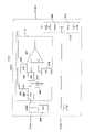
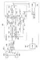
図1は、第1の実施の形態例の同期検波部1000の構成を示す。
ここでは、生産ラインに設置された三相交流モータを、診断対象の回転機1500とする。回転機(三相交流モータ)1500は、サーボアンプ1501と3本の電力線(それぞれu相、v相、w相)で接続され、サーボアンプ1501から供給される三相交流電源で駆動される。<Example of the first embodiment>
First, an example of the first embodiment of the present invention will be described with reference to FIGS. 1 to 15.
FIG. 1 shows the configuration of the
Here, the three-phase AC motor installed on the production line is the
ここで、3本の電力線の内の少なくとも1本(ここでは一例としてw相の電力線)に、電流検知器(カレントトランスフォーマ)1502が接続され、電流検知器1502がw相の電流をモニタリングする。なお、電流検知器1502は、回転機1500に流れる電流の大きさに応じて、適切に選択されなければならない。すなわち、電流容量の大きなモータに対して、許容電流容量の小さな電流検知器を適用すると、電流検知器が破損する恐れがあるので注意を要する。また、逆に電流容量の小さなモータに対して許容電流容量の大きな電流検知器を適用すると、電流信号が検出できなくなる。 Here, a current detector (current transformer) 1502 is connected to at least one of the three power lines (here, as an example, a w-phase power line), and the
電流検知器1502で得られた電流の検知信号は、直交検波部1000に供給される。
直交検波部1000は、アナログフロントエンド1100、デジタル信号処理部1200、通信回路1300、および電源回路1400から構成される。The current detection signal obtained by the
The
アナログフロントエンド1100には、電流検知器1502の出力CTOPおよびCTONが入力される。アナログフロントエンド1100は、入力回路1110とアナログデジタル変換回路1120とを備える。
入力回路1110は、レベル変換および入力フィルタ処理を行い、出力CONDOを得る。入力回路1110の出力CONDOは、アナログデジタル変換回路1120に供給される。入力回路1110の詳細構成の例については後述する(図2)。
アナログデジタル変換回路1120は、入力のアナログ信号をデジタル化して、出力ADCOを得る。アナログデジタル変換回路1120の出力ADCOは、デジタル信号処理部1200に供給される。The outputs CTOP and CTON of the
The
The analog-to-
デジタル信号処理部1200は、ゲイン制御用ミキサ1201、周波数制御用ミキサ1202、ゲイン制御用低域通過フィルタ1203、周波数制御用低域通過フィルタ1204、および目標ゲイン設定用引き算器1205を備える。また、デジタル信号処理部1200は、ゲイン制御器1206、周波数制御器1207、帯域通過フィルタ1208、可変制御発振回路1209、復調信号生成用ミキサ1210,1211、および出力演算部1212を備える。 The digital
そして、デジタル信号処理部1200には、上位システム(クラウド計算機130:図3)から通信回路1300が受信した、可変制御発振器1209の中心周波数設定値FCENTER、周波数ゲインFSTEP、ゲイン制御乗数PIDGCONST、周波数制御乗数PIDFCONST、およびゲイン制御目標値REFが入力される。
また、デジタル信号処理部1200の出力OUTは、通信回路1300を経由して図3に示す上位システム(クラウド計算機130)に送信される。Then, the digital
Further, the output OUT of the digital
次に、直交検波部1000のデジタル信号処理部1200のゲイン制御パスについて説明する。
ゲイン制御用ミキサ1201では、アナログデジタル変換回路1120の出力ADCOと、復調信号生成用ミキサ1210の出力COSの掛け算が行われ、ゲイン制御用ミキサ1201の出力GMIXが、ゲイン制御用低域通過フィルタ1203に供給される。ゲイン制御用低域通過フィルタ1203で低域を通過させることで、後段の制御器における積分ゲインを増大することができる。モータ電流に対する同期検波では速度を必要としないため、積分制御を有効活用することで誤差の少ない制御が可能となる。Next, the gain control path of the digital
In the
ゲイン制御用低域通過フィルタ1203で低域を通過させた出力GLPF1は、目標ゲイン設定用引き算器1205に供給される。
目標ゲイン設定用引き算器1205では、出力GLPF1からゲイン制御目標値REFを減算する演算(GLPF1-REFの演算)が行われ、演算出力GSUBが得られる。目標ゲイン設定用引き算器1205の演算出力GSUBは、ゲイン制御器1206に供給される。ゲイン制御器1206では、ゲイン制御乗数PIDGCONSTが演算出力GSUBに乗算され、ゲイン制御出力GPIDが得られる。The output GLPF1 that has passed the low frequency band by the gain control low
In the target
ゲイン制御器1206が出力するゲイン制御出力GPIDは、このゲイン制御出力GPIDの特定周波数帯域を通過させるため帯域通過フィルタ1208に供給される。帯域通過フィルタ1208の出力は、出力演算部1212に供給される。
なお、ゲイン制御器1206のゲイン制御出力GPIDは、復調信号生成用ミキサ1210,1211にも供給される。復調信号生成用ミキサ1210では、可変制御発振回路1209の一つの出力COS0と、ゲイン制御出力GPIDとが乗算され、乗算出力COSがゲイン制御用ミキサ1201に供給される。また、復調信号生成用ミキサ1211では、可変制御発振回路1209のもう1つの出力SIN0と、ゲイン制御出力GPIDとが乗算され、乗算出力SINが周波数制御用ミキサ1202に供給される。The gain control output GPID output by the
The gain control output GPID of the
次に、直交検波部1000のデジタル信号処理部1200の周波数制御パスについて説明する。
周波数制御用ミキサ1202では、アナログデジタル変換回路1120の出力ADCOと、復調信号生成用ミキサ1211の出力SINの掛け算が行われ、周波数制御用ミキサ1202の出力FMIXが、周波数制御用低域通過フィルタ1204に供給される。Next, the frequency control path of the digital
In the
周波数制御用低域通過フィルタ1204で低域を通過させた出力FLPF1は、周波数制御器1207に供給される。周波数制御器1207では、周波数制御乗数PIDFCONSTが出力FLPF1に乗算され、周波数制御出力FPIDが得られる。
周波数制御器1207が出力する周波数制御出力FPIDは、出力演算部1212に供給される。
また、周波数制御器1207が出力する周波数制御出力FPIDは、可変制御発振回路1209にも供給される。可変制御発振回路1209は、周波数制御出力FPIDと、通信回路1300から得られた周波数ゲインFSTEPおよび中心周波数設定値FCENTERに基づいて、発振出力COS0およびSIN0を生成する。The output FLPF1 that has passed the low frequency band by the frequency control low
The frequency control output FCID output by the
Further, the frequency control output FCID output by the
出力演算部1212は、ゲイン制御出力GBPFと周波数制御出力FPIDを適切に処理して、送信用信号OUTを生成する。例えば各種フィルタ処理、出力用のコード変換、CRC演算等が考えられる。これらはシステム構成に応じて柔軟に設計すればよい。
なお、図11の例で後述するように、出力演算部1212が高速フーリエ変換(FFT)の演算を行い、周波数解析を行うようにしてもよい。但し、出力演算部1212が行うFFT演算は、ゲイン制御出力GBPFに対して行う演算であり、電流検知器1502の出力を直接FFT演算する場合に比べて、非常に低いサンプリングレートで実行できる。
出力演算部1212で得られた送信用信号OUTは、通信回路1300から図3に示す上位システム(クラウド計算機130)に送信される。The
As will be described later in the example of FIG. 11, the
The transmission signal OUT obtained by the
なお、直交検波部1000の電源回路1400には、例えば電池1401が接続され、直交検波部1000内の各回路を作動させる電源電圧VCCを得る。電池1401を使用するのは一例であり、図1に破線で接続を示すように、太陽電池セル1402などの環境発電を設置して、電源回路1400が電源電圧VCCを得るようにしてもよい。なお、環境発電は、電池1401と併用してもよい。 For example, a
図2は、アナログフロントエンド1100の入力回路1110の回路構成例を示す。
入力回路1110は、低域通過フィルタ1111、入力ロード1112、およびレベルシフタ1113を備える。
入力ロード1112は、電流検知器1502の2つの入力CTOPおよびCTONを架橋する抵抗性負荷308から構成される。抵抗性負荷308の大きさは、適用する電流検知器1502に依存して設計する必要がある。FIG. 2 shows a circuit configuration example of the
The
The
レベルシフタ1113は、入力回路1110の後段に接続されたアナログデジタル変換回路1120に対して、入力レベルを調整する機能を持つ。すなわち、レベルシフタ1113は、電源電圧VCCと接地電位GNDの間を、ハイ側分圧抵抗器309とロウ側分圧抵抗器310で分圧して、適切に調整したレベルを電流検知器1502の一方の入力CTONに印加する。ここで決めた基準レベルは、低域通過フィルタ1111の動作にも影響することを考慮して設計する必要がある。 The
低域通過フィルタ1111は、4個の抵抗器301,302,304,306と2個のコンデンサ303,305とオペアンプ307から構成されるアクティブアンプである。アクティブアンプは、パッシブアンプに比較してゲインを調整できるという利点がある。
低域通過フィルタ1111で得られた出力CONDOは、アナログデジタル変換回路1120(図1)に供給される。The low frequency pass filter 1111 is an active amplifier composed of four
The output CONDO obtained by the low frequency pass filter 1111 is supplied to the analog-to-digital conversion circuit 1120 (FIG. 1).
図3は、回転機診断システム100の全体構成例を示す図である。
回転機診断システム100は、複数の計測サイト110a~110mと、ネットワーク120と、クラウド計算機130とを備える。
計測サイト110a~110mは、生産ラインの回転機1500の設置数に応じた任意の数だけ設置される。システム構成によっては、1個の計測サイト110aだけを設ける場合もある。
図3では、1個の計測サイト110aの構成を示すが、他の計測サイト110b~110mも、同様の構成である。
計測サイト110a~110mは、回転機1500を計測する複数の回転機計測ユニット111a~111nと、各回転機計測ユニット111a~111nが出力するパケットPKT1,PKT2,・・・,PKTnを収集するデータ収集装置112とを備える。回転機計測ユニット111a~111nも、生産ラインの回転機1500の設置数に応じた任意の数だけ設置される。システム構成によっては、1個の回転機計測ユニット111aだけを設ける場合もある。FIG. 3 is a diagram showing an overall configuration example of the rotary machine
The rotary machine
The
FIG. 3 shows the configuration of one
The
それぞれの回転機計測ユニット111a~111nは、回転機1500の電流をモニタリングする電流検知器1502と、電流検知器1502が検知した電流を検波する直交検波部1000とを備える。
それぞれの回転機計測ユニット111a~111nの直交検波部1000が備える通信回路1300(図1)は、回転機の計測データが含まれるパケットPKT1,PKT2,・・・,PKTnを出力する。
データ収集装置112は、各回転機計測ユニット111a~111nからのパケットP~PKTnを、ネットワーク120を介してクラウド計算機130に伝送する。Each of the rotating
The communication circuit 1300 (FIG. 1) included in the
The
クラウド計算機130では、受信したパケットPKT1~PKTnに含まれるデータを蓄積する。そして、クラウド計算機130が備える演算ノード131で、蓄積したデータを使った様々な処理が施される。演算ノード131の情報は、回転機を用いた生産ラインの監視を行うシステムから参照され、回転機の劣化状況に合わせたオペレーションに役立てる処理が行われる。これにより機器のダウンタイムを最小にすることが期待され、オペレーションコストの低減に寄与する。 The
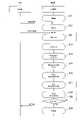
図4は、クラウド計算機130の演算ノード131からの指示で、特定の計測サイト110aの直交検波部1000を起動させる起動シーケンスを示す。
演算ノード131が起動させる前の状態のとき、直交検波部1000は、スリープモードであり、計測を行わない状態で待機している(ステップS11)。このように直交検波部1000がスリープモードに待機することで、回転機計測ユニット111aの消費電力を低減することができる。したがって、各回転機計測ユニット111a~111nを構成する端末を電池駆動する際の電池寿命を延ばすことができ、回転機診断システム100の運用コストを低減することができる。FIG. 4 shows an activation sequence for activating the
When the
ここで、演算ノード131から計測サイト110aに起動信号WAKEUPが伝送されると、該当する計測サイト110aの直交検波部1000が、アクティブ状態に遷移する(ステップS12)。その後、必要に応じて演算ノード131からの下り通信PKTDOWNが送信され、測定条件が設定される。この下り通信PKTDOWNでの測定条件の設定は、毎回行わなくてもよい。例えば、予め設定した動作条件を、計測サイト110aを設置した後に変更したいときに行うようにしてもよい。 Here, when the activation signal WAKEUP is transmitted from the
そして、計測サイト110aの直交検波部1000は、初期化動作を行い(ステップS13)、設定状態での周波数制御およびゲイン制御を実行し(ステップS14)、同期検波動作の準備に入り(ステップS15)、同期検波による測定を開始する(ステップS16)。ここでは、例えば各制御が静定したことを通知する信号を内部で作成し、この信号を計測開始トリガ信号として活用する方法が考えられる。制御が静定したことを検出するには、制御結果と制御目標との差分をモニタリングし、モニタリングした差分が所定の設定値よりも小さくなることを検出する方法が一例として考えられる。 Then, the
その後、計測サイト110aの直交検波部1000は、同期検波による測定を終了する(ステップS17)。この測定の終了は、例えば測定開始からの時間を内部のタイマで測定し、所定の時間になったら終了する。この測定開始などの時間も、測定設定値として下り通信で設定できるようにしてもよい。このようにすることで、運用コストを低減することができる。 After that, the
測定が終了すると、直交検波部1000が備える通信回路1300(図1)が、測定結果のデータを上り通信で送信する(ステップS18)。演算ノード131は、受信した測定結果のデータに基づいた演算処理で、回転機の状態を診断する。
そして、計測サイト110aの直交検波部1000は、上りデータ通信終了後、スリープ状態になり、次のWAKEUP信号の受信まで待機する(ステップS19)。When the measurement is completed, the communication circuit 1300 (FIG. 1) included in the
Then, the
次に、本実施の形態例の直交検波部1000での検波により、回転機の状態を計測する動作について説明する。
図5は直交検波部1000への入力信号(電流検知器1502の出力信号)のスペクトル解析例である。図5の横軸は周波数、縦軸は各周波数でのパワーを示す。
図5に示す波形の中央の周波数位置は主ピーク200である。そして、主ピークの周波数位置f0を中心として、第一側帯波201,202と、第二側帯波203,204が発生している。ここで、第一側帯波201,202や第二側帯波203,204が異常な状態であるとき、回転機1500に劣化などの異常があることが知られており、直交検波部1000では、側帯波201,202,203,204から回転機1500の状態を計測している。Next, an operation of measuring the state of the rotating machine by detecting with the
FIG. 5 is an example of spectrum analysis of an input signal (output signal of the current detector 1502) to the
The frequency position at the center of the waveform shown in FIG. 5 is the
主ピーク200の周波数f0と第一の側帯波201,202との周波数差はdf1である。同様に、主ピーク200の周波数f0と第二の側帯波203,204との周波数差はdf2である。
直交検波部1000では、主ピーク200に対して検波することで、主ピーク200の周波数f0が直流および2倍の高調波2f0に変換され、第一の側帯波201,202は周波数df1へ、第二の側帯波203,204は周波数df2へ移動する。
したがって、直交検波部1000で同期検波した後に、高周波側(2f0)に移動したピークを低域通過フィルタで取り除き、さらに帯域通過フィルタで除去することで、側帯波のみを含む信号を抽出することが可能になる。The frequency difference between the frequency f0 of the
In the
Therefore, after synchronous detection by the
図5に示すスペクトルから回転機1500の異常を早期検出するには、微弱な側帯波201,202の強度を測定する必要があり、このためには主ピーク200を直交検波により除去することが非常に有効である。 In order to detect the abnormality of the
図6は、入力回路1110が備える低域通過フィルタ1111の周波数特性の決め方を示す図である。図6(a)は、低域通過フィルタ1111への入力信号の周波数特性を示し、図6(b)は、低域通過フィルタ1111の通過特性を示す。図6(a)の横軸は周波数、縦軸は振幅を示す。図6(b)の横軸は周波数、縦軸はゲインを示す。 FIG. 6 is a diagram showing how to determine the frequency characteristics of the low frequency pass filter 1111 included in the
周波数f0の主ピーク200の近傍の側帯波として異常信号が検出されることを考慮すると、低域通過フィルタ1111(図2)は、最低でも主ピーク200の周波数f0を通過させるように設計するのが好ましい。この場合、低域通過フィルタ1111のカットオフ周波数fcは、f0<fcを満たすように設計するのが好ましい。後段の回路で低周波のサンプリングが発生する場合には、カットオフ周波数fcをあまり高周波にしすぎないよう設計することで、雑音の折り返しを抑制することができる。カットオフ周波数fcは、主ピーク200の周波数f0よりは大きくするものの、できる限り小さい周波数にすることが精度良い側帯波の検出には有効である。 Considering that an abnormal signal is detected as a sideband wave in the vicinity of the
図7は、図1に示す直交検波部1000の各部の波形の例を示す。図7に示す各波形図の横軸は時間である。
図7(a)は、電流検知器1502の2つの出力CTOP,CTONを示す。図7(a)の縦軸は電圧である。
電流検知器1502の一方の出力CTOPは、アナログ波形なので高周波雑音が重畳されている。電流検知器1502の他方の出力CTONは、レベルシフタ1113(図2)により生成された電位に調整された電圧である。FIG. 7 shows an example of the waveform of each part of the
FIG. 7A shows the two outputs CTOP and CTON of the
Since one output CTOP of the
図7(b)は、入力回路1110の低域通過フィルタ1111を通過した信号CONDOを示す。図7(b)の縦軸は電圧である。
図7(b)に示すように、低域通過フィルタ1111を通過した信号CONDOは、電流検知器1502の出力CTOPから高周波雑音が除去された滑らかな波形になる。FIG. 7B shows the signal CONDO that has passed through the low frequency pass filter 1111 of the
As shown in FIG. 7B, the signal CONDO that has passed through the low frequency pass filter 1111 has a smooth waveform in which high frequency noise is removed from the output CTOP of the
図7(c)は、直交検波部1000のデジタル信号処理部1200のゲイン制御パスの値(LSB)の変化を示す。
ゲイン制御用ミキサ1201の出力GMIXは、信号CONDOの波形(図7(b))に対し、復調信号生成用ミキサ1210が出力する信号COSがローレベル“Low”のときにはマイナスを掛け算して折り返し、ハイレベル“High”のときにはスルーする。
図7(c)に示すように、ゲイン制御用ミキサ1201の出力GMIXを、ゲイン制御用低域通過フィルタ1203でローパス処理すると平坦な波形の出力GLPF1が得られる。このゲイン制御用低域通過フィルタ1203の出力GLPF1から、目標ゲイン設定用引算回路1205でゲイン制御目標値REFを減算することで、出力GSUBが得られ、制御が安定すると出力GSUBが基準レベルに静定する。FIG. 7C shows a change in the value (LSB) of the gain control path of the digital
The output GMIX of the
As shown in FIG. 7 (c), when the output GMIX of the
図7(d)は、直交検波部1000のデジタル信号処理部1200の周波数制御パスの値(LSB)の変化を示す。
周波数制御用ミキサ1201の出力FMIXは、信号CONDOの波形(図7(b))に対し、復調信号生成用ミキサ1211が出力する信号SINがローレベル“Low”のときにはマイナスを掛け算して折り返し、ハイレベル“High”のときにはスルーする。
図7(d)に示すように、周波数制御用ミキサ1201の出力FMIXを、周波数制御用低域通過フィルタ1204でローパス処理すると平坦な波形の出力FLPFが得られ、制御が安定すると出力FLPFが図7に示すように通り基準レベルに静定する。FIG. 7D shows a change in the value (LSB) of the frequency control path of the digital
The output FMIX of the
As shown in FIG. 7D, when the output FMIX of the
これらのゲイン制御出力GPIDと周波数制御出力FPIDは、積分成分を含むためゼロにならない。ゲイン制御出力GPIDに関しては、側帯波がない場合には直流波形に、側帯波が存在する場合には、直流成分に側帯波成分が重畳された波形となる。周波数制御出力FPIDは、周波数制御が安定している限り一定の値をとることになり、これは図5におけるf0に相当する値となる。 These gain control output GPID and frequency control output FCID do not become zero because they include an integral component. Regarding the gain control output GPID, when there is no sideband wave, it becomes a waveform in which the sideband wave component is superimposed on the DC component, and when there is a sideband wave, it becomes a waveform. The frequency control output FCID takes a constant value as long as the frequency control is stable, which is a value corresponding to f0 in FIG.
図8は、ゲイン制御用低域通過フィルタ1203に供給される信号GMIXの波形(図8(a))と、ゲイン制御用低域通過フィルタ1203の通過特性(図8(b))と、ゲイン制御用低域通過フィルタ1203を通過させた後の波形(図8(c))を示す。図8の各図の横軸は周波数、縦軸はゲインである。 FIG. 8 shows the waveform of the signal GMIX supplied to the gain control low-pass filter 1203 (FIG. 8A), the passage characteristics of the gain control low-pass filter 1203 (FIG. 8B), and the gain. The waveform (FIG. 8 (c)) after passing through the control low-
ゲイン制御用低域通過フィルタ1203の入力信号GMIXは、同期検波後の振動であるため、図8(a)に示すように、図5の主ピークの周波数f0は、直流と2倍の周波数2f0へ移動し、第一および第二側帯波のピークが、周波数df1およびdf2に観測される。
ただし、この状態では主ピークの2倍波2f0の成分の強度が圧倒的に大きいため、ゲイン制御用低域通過フィルタ1203でこれをカットする必要がある。よって、図8(b)に示すように、ゲイン制御用低域通過フィルタ1203のカットオフ周波数fc1は、主ピークの2倍波2f0よりも小さくする必要がある。一方で、第二側帯波df2の周波数よりは大きくないと、回転機の異常を観測する信号成分を失ってしまう。Since the input signal GMIX of the low
However, in this state, the intensity of the component of the double wave 2f0 of the main peak is overwhelmingly large, so it is necessary to cut this with the gain control low
これらの条件から、ゲイン制御用低域通過フィルタ1203のカットオフ周波数fc1は、df2<fc1<2f0と設定する必要がある。またゲイン制御用ミキサ1201が理想的な特性を有していない場合、主ピークの1倍波f0成分が大きな強度を持つことがある。これを抑制するためには、カットオフ周波数fc1は、df2<fc1<f0と設定することがより好ましい。 From these conditions, the cutoff frequency fc1 of the gain control low
図8(c)に示す信号GLPF1は、ゲイン制御用低域通過フィルタ1203を通過した後の信号であり、主ピークの2倍波2f0成分が抑制され、側帯波成分が精度良く抽出できる準備ができた信号になっている。
しかしながら、図8(c)に示す信号GLPF1では、低周波側にまだ取り除けていない雑音(図中のNoise)が残存する。この低周波雑音は、帯域通過フィルタ1208(図1)で除かれる。The signal GLPF1 shown in FIG. 8C is a signal after passing through the gain control low
However, in the signal GLPF1 shown in FIG. 8C, noise (Noise in the figure) that has not yet been removed remains on the low frequency side. This low frequency noise is removed by the bandpass filter 1208 (FIG. 1).
次に、図9を用いて、低周波雑音を取り除く帯域通過フィルタ1208の特性を説明する。図9に示す各特性図の横軸は周波数、縦軸はゲインである。図9(a)は、ゲイン制御器1206の出力GPIDのスペクトルを示す。図9(b)は、帯域通過フィルタ1208の周波数特性を示す。図9(c)は、帯域通過フィルタ1208を通過した後の波形GBPFのスペクトルである。 Next, the characteristics of the
ゲイン制御器1206の出力GPIDには、低周波側に雑音(図中のNoise)が残っているため、周波数fc2から周波数fc3を通過帯域に持つ帯域通過フィルタ1208により、この雑音を除去する。この際、下側のカットオフ周波数fc2は、雑音周波数をfnとすると、fn<fc2<df1となるように設定し、下側のカットオフ周波数fc3は、df2<fc3<2f0となるように設定するのが好ましい。これにより、図9(c)に示すように、低周波側の雑音が除去され、側帯波成分df1およびdf2を、精度良く抽出することが可能となる。 Since noise (Noise in the figure) remains in the output GPID of the
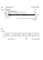
図10(a)は、帯域通過フィルタ1208の出力GBPFの時系列波形の例を示す。図10(a)において、横軸は時間、縦軸は値(LSB)を示す。
また、図10(b)は、出力GBPFが得られた場合の、通信回路1300が送信する通信ペイロードのパケットPKTUPの構成の一例である。FIG. 10A shows an example of a time-series waveform of the output GBPF of the
Further, FIG. 10B is an example of the configuration of the packet PKTUP of the communication payload transmitted by the
図10(a)に示すように、起動してからゲイン制御出力が静定するよりも前の時間帯(Init)は起動シーケンスとして定義しておき、出力演算部1212は、この期間(Init)を除いた出力の交流振幅値MAGを最終出力とする。この交流振幅値MAGは、第一および第二側帯波の成分を含んだ強度になっている。よって、回転機1500が劣化した時には、交流振幅値MAGの値が大きくなり、正常の場合にはゼロに近い値になる。 As shown in FIG. 10A, the time zone (Init) before the gain control output is settled after the start is defined as the start sequence, and the
上り通信のパケットPKTUPには、図10(b)に示すように、センサ状態を示す情報(sensor Condition)、交流振幅値MAGおよび周波数制御出力FPIDなどのデータ(Data)、信頼性担保情報(CRC)が配置されている。
センサ状態を示す情報には、センサ固有番号sensorID、バッテリ残量情報batt、温度情報tempといった情報が含まれる。このような情報が含まれるパケットPKTUPをシステムの上位(クラウド計算機130の演算ノード131)に送信することで、診断結果をシステムの上位で演算することが可能になる。As shown in FIG. 10B, the uplink communication packet PKTUP includes information indicating the sensor status (sensor Condition), data such as AC amplitude value MAG and frequency control output FCID (Data), and reliability assurance information (CRC). ) Is placed.
The information indicating the sensor status includes information such as the sensor unique number sensorID, the battery remaining amount information butt, and the temperature information mp. By transmitting the packet PKTUP containing such information to the upper level of the system (
具体的には、交流振幅値MAGの大きさは異常そのものを示し、周波数制御出力FPIDは同期検波が正常に動作しているかを確認するのに役立つ。さらに、主ピークの周波数f0は回転機1500の駆動スピードと連動するため、多数の回転機1500を同時にモニタリングしている状況では、搬送ライン全体の健全度を主ピークの周波数f0から判断できるようになる。 Specifically, the magnitude of the AC amplitude value MAG indicates the abnormality itself, and the frequency control output FCID is useful for confirming whether the synchronous detection is operating normally. Furthermore, since the frequency f0 of the main peak is linked to the drive speed of the
次に、図1に示す出力演算部1212が、第一側帯波と第二側帯波のスペクトルを得る演算を行った場合の例を説明する。すなわち、図10に示す例では、交流振幅値MAGを上位側に送信するようにしたが、第一側帯波と第二側帯波のスペクトルを解析して、それぞれの強度を上位側に送信してもよい。出力演算部1212が第一側帯波と第二側帯波のスペクトルを解析する場合には、出力演算部1212が高速フーリエ変換(FFT)の演算を行う。ここでのFFT演算は、交流振幅値MAGをFFT演算してスペクトルを得る演算であり、生データをFFTするのに比較して、側帯波は非常に低周波(数Hz)であることからサンプリングレートを低くでき、演算量を低く抑えることが可能になる。 Next, an example will be described in which the
図11は、出力演算部1212が交流振幅値MAGから第一側帯波と第二側帯波のスペクトルを解析した場合の例を示す。
図11(a)は、交流振幅値MAGのスペクトルを示す。図11(a)の横軸は周波数、縦軸はゲインである。
図11(b)は、交流振幅値MAGのスペクトルを解析して得られた第一側帯波と第二側帯波の強度および周波数を配置した送信パケットの構成例を示す。FIG. 11 shows an example in which the
FIG. 11A shows a spectrum of the AC amplitude value MAG. The horizontal axis of FIG. 11A is frequency, and the vertical axis is gain.
FIG. 11B shows a configuration example of a transmission packet in which the intensities and frequencies of the first side band wave and the second side band wave obtained by analyzing the spectrum of the AC amplitude value MAG are arranged.
図11(a)に示す交流振幅値MAGを周波数解析した場合、第一側帯波の強度MAG1および周波数df1と、第二側帯波の強度MAG2および周波数df2とが得られる。
このようにして得られた第一側帯波の強度MAG1および周波数df1、ならびに第二側帯波の強度MAG2および周波数df2を、図11(b)に示すように、通信回路1300が送信する通信ペイロードのパケットPKTUPのデータ(Data)に配置する。パケットPKTUPのその他の内容は、図10(b)の構成と同じである。When the AC amplitude value MAG shown in FIG. 11A is frequency-analyzed, the intensity MAG1 and the frequency df1 of the first sideband wave and the intensity MAG2 and the frequency df2 of the second sideband wave are obtained.
The intensity MAG1 and frequency df1 of the first sideband wave thus obtained, and the intensity MAG2 and frequency df2 of the second sideband wave are shown in FIG. 11B of the communication payload transmitted by the
図12は、システム上位(図3のクラウド計算機130)からダウンリンクで、通信回路1300が受信するパケットPKTDOWNの構成の一例を示す。
パケットPKTDOWNには、情報を識別するためのsensorIDと、設定データsetingと、CRC情報とを配置する。
設定データsetingとしては、周波数制御乗数PIDFCONST、ゲイン制御乗数PIDGCONST、可変制御発振回路の中心周波数FCENTER、制御発信機の周波数ゲインFSTEP、およびゲイン制御目標REFが配置される。FIG. 12 shows an example of the configuration of the packet PKTDOWN received by the
In the packet PKTDOWN, a sensorID for identifying information, setting data setting, and CRC information are arranged.
As the setting data setting, the frequency control multiplier PIDFCONST, the gain control multiplier PIDGCONST, the center frequency FCENTER of the variable control oscillation circuit, the frequency gain FSTEP of the control transmitter, and the gain control target REF are arranged.
なお、これらの設定データは、起動時に毎回送信する必要はなく、例えば同期検波がうまく行かない場合や、装置の設置時に送信され、各計測サイト側では受信した設定データが記憶される。このようにすることで、ダウンリンクの通信を必要最低限に抑えることができ、システム運用のための消費電力を小さくすることができる。特に、ダウンリンクの通信は消費電力が大きく、ダウンリンクの通信回数を減らすことで、より大きな効果がある。 It should be noted that these setting data do not need to be transmitted every time at startup, for example, they are transmitted when synchronous detection does not go well or when the device is installed, and the received setting data is stored on each measurement site side. By doing so, downlink communication can be suppressed to the minimum necessary, and power consumption for system operation can be reduced. In particular, downlink communication consumes a large amount of power, and reducing the number of downlink communication has a greater effect.
なお、図1に示す直交検波部1000では、アナログフロントエンド1100のアナログデジタル変換回路1120でデジタル変換されたデータを処理するようにした。これに対して、直交検波部1000が入力回路1110のアナログ信号としての出力CONDOを入力として、直交検波部1000内でデジタル変換するようにしてもよい。 The
図13および図14は、直交検波部1000がアナログデジタル変換回路を備える場合の構成例を示す。
図13に示す例では、アナログフロントエンド1100は入力回路1110を備え、入力回路1110の出力CONDO(アナログ信号)を、デジタル信号処理部1200に供給する。デジタル信号処理部1200は、ゲイン制御用ミキサ1201および周波数制御用ミキサ1202でアナログ信号処理を行い、ゲイン制御用ミキサ1201の出力GMIXおよび周波数制御用ミキサ1202の出力FMIXを得る。13 and 14 show a configuration example when the
In the example shown in FIG. 13, the analog
そして、ゲイン制御用ミキサ1201の出力GMIXをアナログデジタル変換回路1213に供給してデジタル出力GADCを得、このデジタル出力GADCをゲイン制御用低域通過フィルタ1203に供給する。
また、周波数制御用ミキサ1202の出力FMIXをアナログデジタル変換回路1214に供給してデジタル出力FADCを得、このデジタル出力FADCを周波数制御用低域通過フィルタ1204に供給する。
図13に示す直交検波部1000のその他の箇所は、図1に示す直交検波部1000と同様に構成する。Then, the output GMIX of the
Further, the output FMIX of the
Other parts of the
図14に示す例は、さらに、ゲイン制御用低域通過フィルタ1203および周波数制御用低域通過フィルタ1204もアナログ回路とし、両フィルタ1203および1204の後段に、アナログデジタル変換回路1215および1216を配置した例である。
この場合、ゲイン制御用低域通過フィルタ1203は、出力GLPF1をアナログデジタル変換回路1215に供給し、変換されたデジタル信号GADCを目標ゲイン設定用引算回路1205に供給する。また、周波数制御用低域通過フィルタ1204は、出力FLPF1をアナログデジタル変換回路1216に供給し、変換されたデジタル信号FADCを周波数制御器1207に供給する。
図14に示す直交検波部1000のその他の箇所は、図13に示す直交検波部1000と同様に構成する。In the example shown in FIG. 14, the low-
In this case, the gain control low
Other parts of the
この図13および図14に示すように、直交検波部1000の内部でデジタル変換処理を行うように構成した場合にも、図1の構成と同様に、第一側帯波と第二側帯波の強度に応じた信号を得ることができる。 As shown in FIGS. 13 and 14, even when the digital conversion process is performed inside the
また、ここまで説明した構成では、直交検波部1000が備える電源回路1400として、電池1401または環境発電を備える構成とした。これに対して、電源1400として、回転機1500に接続された電力線から検知した電流を電源として使用してもよい。
すなわち、図15に示すように、回転機1500のu相の電力線に、電力検知器1503を配置し、電力検知器1503で得た電流を、電源回路1400に供給する。u相の電力線から電流を得るのは一例であり、その他の相の電力線でもよい。但し、異常を検知するための電力検知器1502とは別の相の電力線から電流を得るのが好ましい。Further, in the configuration described so far, the
That is, as shown in FIG. 15, the
そして、電源回路1400は、電力検知器1503で得た電流から、直交検波部1000を作動させる電源電圧VCCを得る。
図15に示す直交検波部1000のその他の構成については、図1に示す直交検波部1000と同様に構成する。
このようにして、回転機1500を駆動させる電力から、直交検波部1000を作動させる電源を得るようにしたことで、電池などが不要になり、電源構成を簡単にすることができる。Then, the
Other configurations of the
In this way, by obtaining the power source for operating the
<第2の実施の形態例>
次に、本発明の第2の実施の形態例を、図16~図18を参照して説明する。図16~図18において、第1の実施の形態例で説明した図1~図15と同一箇所には同一符号を付し、重複説明を省略する。<Example of the second embodiment>
Next, an example of the second embodiment of the present invention will be described with reference to FIGS. 16 to 18. In FIGS. 16 to 18, the same parts as those in FIGS. 1 to 15 described in the first embodiment are designated by the same reference numerals, and duplicate description will be omitted.
図16は、第2の実施の形態例における直交検波部1000の構成を示す図である。
図16に示す直交検波部1000は、図1に示す可変制御発振回路1209の代わりに、周波数演算部1701を設けている。また、デジタル信号処理部1200として、入力ADCOをラッチするデータラッチ1601と、乗算論理部1602,1603,1604,1605とを備える。FIG. 16 is a diagram showing the configuration of the
The
すなわち、デジタル信号処理部1200のデータラッチ1601は、周波数演算部1701から供給されるクロックCKに同期して、入力ADCOをラッチして、ラッチ出力LTOを得る。なお、データラッチ1601は、主ピークの周波数に対して非常に早い周波数でサンプリングする。
データラッチ1601のラッチ出力LTOは、乗算論理部1602,1603に供給される。乗算論理部1602は、別の乗算論理部1604の出力COSとラッチ出力LTOとの論理演算出力GMULTを、ゲイン制御用低域通過フィルタ1203に供給する。乗算論理部1604は、ゲイン制御器1206の出力GPIDと、周波数演算部1701の出力COS0との論理演算で、乗算出力COSを得る。That is, the data latch 1601 of the digital
The latch output LTO of the
また、乗算論理部1603は、別の乗算論理部1605の出力SINとラッチ出力LTOとの論理演算出力FMULTを、周波数制御用低域通過フィルタ1204に供給する。乗算論理部1605は、ゲイン制御器1206の出力GPIDと、周波数演算部1701の出力SIN0との論理演算で、乗算出力SINを得る。
周波数演算部1701は、クロックCKを発生させる発振器と、その発振器の出力のカウント動作などに基づいて上述した出力COS0およびSIN0を生成させる回路を備える。Further, the
The
図17は、図16に示す直交検波部1000の各部の波形の例を示す。図17に示す各波形図の横軸は時間である。
図17(a)は、データラッチ1601の出力LTOの変化を示す。出力LTOの波形は、主ピークの周波数に対して非常に早い周波数でサンプリングするため、アナログのように滑らかな波形となる。FIG. 17 shows an example of the waveform of each part of the
FIG. 17A shows a change in the output LTO of the
図17(b)は、図16に示す直交検波部1000のゲイン制御パスの値(LSB)の変化を示す。
乗算論理部1602の論理演算出力GMULTは、乗算論理部1604が出力する信号COSがローレベル“Low”のときにはマイナスを掛け算して折り返し、ハイレベル“High”のときにはスルーする波形になる。
この乗算論理部1602の論理演算出力GMULTを、ゲイン制御用低域通過フィルタ1203でローパス処理すると平坦な波形の出力GLPF1が得られる。このゲイン制御用低域通過フィルタ1203の出力GLPF1から、目標ゲイン設定用引算回路1205でゲイン制御目標値REFを減算することで、出力GSUBが得られ、制御が安定すると出力GSUBが基準レベルに静定する。FIG. 17B shows a change in the value (LSB) of the gain control path of the
The logical operation output GMULT of the
When the logical operation output GMULT of the
図17(c)は、直交検波部1000の周波数制御パスの値(LSB)の変化を示す。
乗算論理部1603の論理演算出力FMULTは、乗算論理部1605が出力する信号SINがローレベル“Low”のときにはマイナスを掛け算して折り返し、ハイレベル“High”のときにはスルーする。
この乗算論理部1603の論理演算出力FMULTを、周波数制御用低域通過フィルタ1204でローパス処理すると平坦な波形の出力FLPFが得られ、制御が安定すると出力FLPFが基準レベルに静定する。
図17に示す波形は、第1の実施の形態例の図7に示す動作波形と同一であり、この図17に示す波形から、第1の実施の形態例と同様に同期検波を行えることが判る。FIG. 17C shows a change in the value (LSB) of the frequency control path of the
The logical operation output FMULT of the
When the logical operation output FMULT of the
The waveform shown in FIG. 17 is the same as the operating waveform shown in FIG. 7 of the first embodiment, and synchronous detection can be performed from the waveform shown in FIG. 17 in the same manner as in the first embodiment. I understand.
図16に示す本実施の形態例の直交検波部1000の場合、デジタル信号処理部1200と周波数演算部1701は、純粋な論理回路であるため、ロジック回路、FPGA、マイクロコンピュータ上で動作するソフトウェアなどの様々な実装方法で、直交検波部1000を構成することができる。
ここで、対象とする回転機の主ピーク周波数に応じて測定系に要求されるスピードが変わるため、スピードに応じて最適な実装方法を選択すればよい。In the case of the
Here, since the speed required for the measurement system changes according to the main peak frequency of the target rotating machine, the optimum mounting method may be selected according to the speed.
なお、図16に示す周波数演算部1701では、発振器の出力を直接クロックCKとしてデータラッチ1601に供給するようにした。これに対して、発振器が出力したクロックCKのカウント値と、周波数制御器1207の周波数制御出力FPIDとを、周波数演算部1701内で比較して、比較結果としてのリセット信号を、データラッチ1601にクロックとして供給してもよい。
このようにデータラッチ1601がリセット信号でラッチ動作を行うことで、ラッチ周期を低減することができ、デジタル信号処理部1200の負荷を低減することができる。
さらに、この場合にはリセット信号でトリガをかけて、アナログデジタル変換回路1120を間欠駆動することで、アナログデジタル変換回路1120における消費電流を低減することができる。In the
By performing the latch operation with the reset signal in this way, the
Further, in this case, the current consumption in the analog-to-
図18は、図16に示す直交検波部1000においてデータラッチ1601がリセット信号でラッチ動作を行う場合の動作波形である。
図18(a)は、データラッチ1601の出力LTOの変化を示す。出力LTOは周波数制御が静定している場合には4f0のサンプリング周波数を有し、アナログ波形であるLTOに対して、図に黒丸で示す位置の値をサンプリングした出力となる。FIG. 18 is an operation waveform when the
FIG. 18A shows a change in the output LTO of the
図18(b)は、図16に示す直交検波部1000のゲイン制御パスの値(LSB)の変化を示す。
乗算論理部1602の論理演算出力GMULTは、乗算論理部1604が出力する信号COSがローレベル“Low”のときにはマイナスを掛け算して折り返し、ハイレベル“High”のときにはスルーする波形になる。アナログ波形が存在した場合の掛け算結果180(図18(b))と、図17(b)における論理演算出力GMULTの波形は異なったものとなる。FIG. 18B shows a change in the value (LSB) of the gain control path of the
The logical operation output GMULT of the
図18(c)は、直交検波部1000の周波数制御パスの値(LSB)の変化を示す。
乗算論理部1603の論理演算出力FMULTは、乗算論理部1605が出力する信号SINがローレベル“Low”のときにはマイナスを掛け算して折り返し、ハイレベル“High”のときにはスルーする。アナログ波形が存在した場合の掛け算結果181(図18(c))と、図17(c)における論理演算出力FMULTの波形は異なったものとなる。
図18に示す波形は、第1の実施の形態例の図7に示す動作波形とサンプリング周波数が異なるもののLSB値としては同一であり、この図18に示す波形から、第1の実施の形態例と同様に同期検波を行えることが判る。FIG. 18C shows a change in the value (LSB) of the frequency control path of the
The logical operation output FMULT of the
The waveform shown in FIG. 18 has a different sampling frequency from the operating waveform shown in FIG. 7 of the first embodiment, but has the same LSB value. From the waveform shown in FIG. 18, the first embodiment is shown. It can be seen that synchronous detection can be performed in the same way as.
図19は、このリセット信号でデータラッチ1601がラッチ動作を行う場合の、入力回路1110が備える低域通過フィルタ1111(図2)の周波数特性を示したものである。図19(a)は、アナログデジタル変換回路1120の出力ADCOの周波数特性を示し、横軸は周波数、縦軸は振幅を示す。図19(a)は、低域通過フィルタ1111の特性を示す、横軸は周波数、縦軸はゲインを示す。 FIG. 19 shows the frequency characteristics of the low frequency pass filter 1111 (FIG. 2) included in the
低域通過フィルタ1111のカットオフ周波数fc4は、主ピークの周波数f0より大きい必要があるが、データラッチ1601のサンプリング周波数は制御が静定している場合、周波数4f0になる。よって、図19(b)に示すように、カットオフ周波数fc4はf0<fc4<4f0を満たすように設定する必要がある。
このように低域通過フィルタ1111のカットオフ周波数4f0を設定することで、データラッチ1601におけるデータ取り込み時の雑音の折り返しを低減し、精度良い計測が可能になる。The cutoff frequency fc4 of the low frequency pass filter 1111 needs to be larger than the frequency f0 of the main peak, but the sampling frequency of the
By setting the cutoff frequency 4f0 of the low frequency pass filter 1111 in this way, it is possible to reduce the turnaround of noise at the time of data capture in the
<変形例>
なお、本発明は、上述した各実施の形態例に限定されるものではなく、様々な変形例が含まれる。例えば、上記した各実施の形態例は、本発明を分かりやすく説明するために詳細に説明したものであり、必ずしも説明した全ての構成を備えるものに限定されるものではない。また、複数の実施の形態例の構成を組み合わせてもよい。<Modification example>
The present invention is not limited to the above-described embodiments, but includes various modifications. For example, each of the above-described embodiments will be described in detail in order to explain the present invention in an easy-to-understand manner, and is not necessarily limited to those having all the described configurations. Further, the configurations of a plurality of embodiments may be combined.
例えば、図1や図3に示す構成では、直交検波部1000が、1つの回転機1500の電流検知器1502の出力信号を検波するようにした。これに対して、1つの直交検波部1000が、複数の電流検知器1502の出力信号を検波してもよい。
図20は、1つの直交検波部1000′が、複数の電流検知器1502の出力信号を検波する場合の構成の例を示す。
図20に示す構成について説明すると、ここではm個(mは任意の整数)の回転機1500a~1500mを用意し、このm個の回転機1500a~1500mごとに、個別に電流検知器1502を設ける。そして、それぞれの電流検知器1502の出力信号を、直交検波部1000′が備えるマルチプレクサ1701に供給する。マルチプレクサ1701は、出力演算部1212から供給される選択信号SELに基づいて、アナログフロントエンド1100に供給する入力信号を、順に切り替える処理を行う。
直交検波部1000′のアナログフロントエンド1100とデジタル信号処理部1200の構成については、図1に示す直交検波部1000と同様の構成である。For example, in the configuration shown in FIGS. 1 and 3, the
FIG. 20 shows an example of a configuration in which one orthogonal detection unit 1000'detects output signals of a plurality of
Explaining the configuration shown in FIG. 20, here, m (m is an arbitrary integer)
The configuration of the analog
図21(a)は、図20に示す構成の直交検波部1000′の場合に、マルチプレクサ1701に供給される選択信号SELと、出力演算部1212に供給されるバンドパスフィルタ1208の出力GBPFを示す。
図21(a)に示すように、m個の電流検知器1502を切り替える選択信号SELをマルチプレクサ1701に送る。この選択信号SELの切り替わりに連動して、1つの電流検知器1502の出力についての、交流振幅値MAGを得る。ここで、それぞれの電流検知器1502の交流振幅値MAGを出力する期間において、起動してからゲイン制御出力が静定するよりも前の時間帯(Init)を定め、その静定するよりも前の時間帯(Init)を除いた期間の交流振幅値MAGを計測する。FIG. 21A shows the selection signal SEL supplied to the
As shown in FIG. 21A, a selection signal SEL for switching m
図21(b)は、図20に示す構成の直交検波部1000′の場合に、通信回路1300が送信する通信ペイロードのパケットPKTUPの構成の一例である。
図21(b)に示すように、パケットPKTUPには、センサ状態を示す情報(sensor Condition)、交流振幅値MAGおよび周波数制御出力FPIDなどのデータ(Data)、信頼性担保情報(CRC)が配置されている。
ここで、データ(Data)の区間には、m個の交流振幅値MAGおよび周波数制御出力FPIDを配置する。FIG. 21B is an example of the configuration of the packet PKTUP of the communication payload transmitted by the
As shown in FIG. 21B, information indicating the sensor state (sensor Condition), data such as AC amplitude value MAG and frequency control output FCID (Data), and reliability assurance information (CRC) are arranged in the packet PKTUP. Has been done.
Here, m AC amplitude value MAGs and frequency control output FCIDs are arranged in the data (Data) section.
図22は、図20に示す構成の直交検波部1000′を備えた場合における、直交検波部1000′を起動させる起動シーケンスを示す。図22において、図4に示す起動シーケンスと同一の処理については、同一のステップ番号を付す。
図22に示すシーケンスが図4に示すシーケンスと相違する点は、ステップS12とステップS13との間に、ステップS21の処理が行われる点と、ステップS18とステップS19との間に、ステップS22の判断処理が行われる点である。FIG. 22 shows an activation sequence for activating the orthogonal detection unit 1000'when the orthogonal detection unit 1000'with the configuration shown in FIG. 20 is provided. In FIG. 22, the same step numbers are assigned to the same processes as those in the activation sequence shown in FIG.
The difference between the sequence shown in FIG. 22 and the sequence shown in FIG. 4 is that the processing of step S21 is performed between steps S12 and S13, and that of step S22 between steps S18 and S19. This is the point where the judgment process is performed.
すなわち、ステップS12で直交検波部1000がアクティブ状態に遷移した後、ステップS21で選択信号SELに基づいたマルチプレクサ1701での選択処理が行われてから、ステップS13の初期化動作に移行する。
また、ステップS18で測定結果のデータを上り通信で送信した後、ステップS22でm個の選択を全て行ったか否かを判断し、m個の選択が行われた場合に(ステップS22のYES)、ステップS19の待機に移る。また、ステップS22でm個の選択を全て行っていない場合(ステップS22のNO)、マルチプレクサ1701に次の選択信号SELを送り、ステップS21からステップS18までの処理を繰り返す。
このようにして、1つの直交検波部1000′が、複数の電流検知器1502の出力信号を検波して、順にクラウド計算機130側に送信することができる。この図20に示す構成とすることで、多数の回転機1500についての検波を、少ない検波部で効率よく行うことができ、システム構成の簡易化につながる。That is, after the
Further, after transmitting the measurement result data by uplink communication in step S18, it is determined whether or not all m selections have been made in step S22, and when m selections have been made (YES in step S22). , Move to the standby of step S19. If all m selections have not been made in step S22 (NO in step S22), the next selection signal SEL is sent to the
In this way, one orthogonal detection unit 1000'can detect the output signals of the plurality of
なお、図20に示す構成や、図1などに示す構成では、アナログフロントエンド1100として、入力回路1110を備えて、入力回路1110の出力CONDOをアナログデジタル変換回路1120に供給して、デジタル変換出力ADCOを得るようにした。これに対して、電流検知器1502の出力を直接、アナログデジタル変換回路1120に供給してデジタル変換するようにしてもよい。例えば、マイクロコンピュータ(いわゆるマイコン)で直交検波部を構成したとき、そのマイコンが備えるアナログデジタル変換回路1120の入力である入力MUXに、電流検知器1502の出力を供給する構成としてもよい。
また、図20に示す構成では、図1に示す第1の実施の形態例の構成に組み合わせた例としたが、第2の実施の形態例において、同様に複数の電流検知器1502の出力信号を、1つの検波部で検波するようにしてもよい。In the configuration shown in FIG. 20 and the configuration shown in FIG. 1, an
Further, in the configuration shown in FIG. 20, an example combined with the configuration of the first embodiment shown in FIG. 1 is used, but in the second embodiment, the output signals of the plurality of
また、第1の実施の形態例や第2の実施の形態例において、検波部が備える低域通過フィルタ1203,1204や、帯域通過フィルタ1208は、実際の作動状態によってノイズなどの除去が不要である場合に、一部または全てを省略してもよい。また、これらのフィルタを設ける場合であっても、図1などに示す接続位置以外の箇所に、低域通過フィルタや帯域通過フィルタを配置してもよい。
また、上述した実施の形態例では、モータである回転機の診断システムとした。これに対して、モータの劣化診断だけでなく、劣化により駆動電流の主ピークの近傍に側帯波を生じるようなモータ以外の回転機の診断にも本発明を適用することが可能である。Further, in the first embodiment and the second embodiment, the low
Further, in the above-described embodiment, a diagnostic system for a rotating machine, which is a motor, is used. On the other hand, the present invention can be applied not only to the diagnosis of deterioration of the motor but also to the diagnosis of a rotating machine other than the motor in which a sideband wave is generated in the vicinity of the main peak of the drive current due to the deterioration.
また、構成図や機能ブロック図では、制御線や情報線は説明上必要と考えられるものだけを示しており、製品上必ずしも全ての制御線や情報線を示しているとは限らない。実際には殆ど全ての構成が相互に接続されていると考えてもよい。 Further, in the configuration diagram and the functional block diagram, only the control lines and information lines considered necessary for explanation are shown, and not all the control lines and information lines are shown in the product. In practice, it can be considered that almost all configurations are interconnected.
また、各実施の形態例で説明した構成は、プロセッサがそれぞれの機能を実現するプログラムを解釈し、実行することによりソフトウェアで実現してもよい。各機能を実現するプログラムなどの情報は、メモリや、ハードディスク、SSD(Solid State Drive)等の記録装置、または、ICカード、SDカード、光ディスク等の記録媒体に置くことができる。 Further, the configuration described in each embodiment may be realized by software by the processor interpreting and executing a program that realizes each function. Information such as a program that realizes each function can be placed in a memory, a hard disk, a recording device such as an SSD (Solid State Drive), or a recording medium such as an IC card, an SD card, or an optical disk.
100…回転機診断システム、110a~110n…計測サイト、111a~111n…回転機計測ユニット、112…データ収集装置、120…ネットワーク、130…クラウド計算機、131…演算ノード、301,302,306…抵抗器、303,305…コンデンサ、307…オペアンプ、308…抵抗性負荷、309…ハイ側分圧抵抗器、310…ロウ側分圧抵抗器、1000,1000′…直交検波部、1100…アナログフロントエンド、1110…入力回路、1111…低域通過フィルタ、1112…入力ロード、1113…レベルシフタ、1120…アナログデジタル変換回路、1200…デジタル信号処理部、1201…ゲイン制御用ミキサ、1202…周波数制御用ミキサ、1203…ゲイン制御用低域通過フィルタ、1204…周波数制御用低域通過フィルタ、1205…目標ゲイン設定用引算回路、1206…ゲイン制御器、1207…周波数制御器、1208…帯域通過フィルタ、1209…可変制御発振回路、1210,1211…復調信号生成用ミキサ、1212…出力演算部、1213,1214,1215,1216…アナログデジタル変換回路、1300…通信回路、1400…電源回路、1401…電池、1402…太陽電池セル、1500,1500a~1500m…回転機(三相交流モータ)、1501…サーボアンプ、1502,1503…電流検知器、1600…デジタル信号処理部、1601…データラッチ、1602,1603,1609…乗算論理部、1604,1605…低域通過フィルタ、1606…引算回路、1607,1608…PIDコントローラ、1609,1610…乗算論理部、1611…帯域通過フィルタ、1612…出力演算部、1701…周波数演算部、1801…マルチプレクサ 100 ... Rotating machine diagnostic system, 110a-110n ... Measurement site, 111a-111n ... Rotating machine measuring unit, 112 ... Data collection device, 120 ... Network, 130 ... Cloud computer, 131 ... Calculation node, 301, 302, 306 ... Resistance Instrument, 303, 305 ... Condenser, 307 ... Operated, 308 ... Resistive load, 309 ... High side voltage dividing resistor, 310 ... Low side voltage dividing resistor, 1000, 1000' ... Orthogonal detector, 1100 ... Analog front end , 1110 ... Input circuit, 1111 ... Low frequency pass filter, 1112 ... Input load, 1113 ... Level shifter, 1120 ... Analog digital conversion circuit, 1200 ... Digital signal processing unit, 1201 ... Gain control mixer, 1202 ... Frequency control mixer, 1203 ... Gain control low pass filter, 1204 ... Frequency control low pass filter, 1205 ... Target gain setting subtraction circuit, 1206 ... Gain controller, 1207 ... Frequency controller, 1208 ... Band pass filter, 1209 ... Variable control oscillation circuit, 1210, 1211 ... Demodulation signal generation mixer, 1212 ... Output calculation unit, 1213, 1214, 1215, 1216 ... Analog digital conversion circuit, 1300 ... Communication circuit, 1400 ... Power supply circuit, 1401 ... Battery, 1402 ... Solar cell, 1500, 1500a ~ 1500m ... Rotator (three-phase AC motor), 1501 ... Servo amplifier, 1502, 1503 ... Current detector, 1600 ... Digital signal processing unit, 1601 ... Data latch, 1602, 1603, 1609 ... Multiplication logic unit, 1604, 1605 ... Low frequency pass filter, 1606 ... Subtraction circuit, 1607, 1608 ... PID controller, 1609, 1610 ... Multiplication logic unit, 1611 ... Band pass filter, 1612 ... Output calculation unit, 1701 ... Frequency calculation Part, 1801 ... multiplexer
Claims (8)
Translated fromJapanese前記電流検知器が検知した電流の主周波数に対して直交検波を行い側帯波の強度を抽出する検波部と、を備え、
前記検波部は通信回路を有し、
前記検波部が抽出した前記側帯波の強度を、前記通信回路からクラウド計算機に送信すると共に、前記通信回路で前記クラウド計算機から送信された前記検波部の動作設定値を受信し、
受信した前記動作設定値に基づいて前記検波部を作動させる
回転機診断システム。A current detector that detects the current of at least one current line connected to the rotating machine,
It is provided with a detection unit that performs orthogonal detection with respect to the main frequency of the current detected by the current detector and extracts the intensity of the sideband wave.
The detection unit has a communication circuit and has a communication circuit.
The intensity ofthe sideband wave extracted by the detection unit is transmitted from the communication circuit to the cloud computer, and the operation setting value of the detection unittransmitted from the cloud computer is received by the communication circuit.
A rotary machine diagnostic system that operates the detection unit based on the received operation setting value.
請求項1に記載の回転機診断システム。The rotary machine diagnostic system according to claim 1, wherein the detection unit has a power supply circuit and is driven by electric power supplied from a battery.
請求項1に記載の回転機診断システム。The rotary machine diagnostic system according to claim 1, wherein the detection unit has a power supply circuit and is driven by electric power obtained by energy harvesting or electric power obtained by detecting the current of the current line.
前記入力フィルタのカットオフ周波数は、少なくとも前記主周波数よりも高い周波数に設定して、前記入力フィルタが前記主周波数の成分を通過させる
請求項1に記載の回転機診断システム。The detector has an analog front-end circuit that includes an input filter that passes below the cutoff frequency.
The rotary machine diagnostic system according to claim 1, wherein the cutoff frequency of the input filter is set to at least a frequency higher than the main frequency, and the input filter passes a component of the main frequency.
前記帯域通過フィルタは直交検波した結果に対して適用される
請求項1に記載の回転機診断システム。The detection unit has a bandpass filter that includes at least the frequency of the sideband wave in the passband.
The rotary machine diagnostic system according to claim 1, wherein the bandpass filter is applied to the result of orthogonal detection.
請求項1に記載の回転機診断システム。The rotary machine diagnostic system according to claim 1, wherein the intensity of the side band is extracted after the operation of the detection unit is settled.
複数組の前記検波部が検波したデータを収集するデータ収集装置と、
前記データ収集装置が収集したデータを蓄積するクラウド計算機とを有する
請求項1に記載の回転機診断システム。A plurality of sets of the current detector and the detection unit are prepared.
A data collection device that collects data detected by a plurality of sets of the detection units, and
The rotary machine diagnostic system according to claim 1, further comprising a cloud computer that stores data collected by the data collection device.
前記データラッチで前記検波部の入力をサンプリングする
請求項1に記載の回転機診断システム。The detector comprises a data latch that samples the input of the detector.
The rotary machine diagnostic system according to claim 1, wherein the input of the detection unit is sampled by the data latch.
Priority Applications (3)
| Application Number | Priority Date | Filing Date | Title |
|---|---|---|---|
| JP2018198117AJP7059161B2 (en) | 2018-10-22 | 2018-10-22 | Rotating machine diagnostic system |
| US16/596,807US11088652B2 (en) | 2018-10-22 | 2019-10-09 | Rotary machine diagnostic system |
| CN201910962509.7ACN111077381B (en) | 2018-10-22 | 2019-10-11 | Rotary Machine Diagnostic System |
Applications Claiming Priority (1)
| Application Number | Priority Date | Filing Date | Title |
|---|---|---|---|
| JP2018198117AJP7059161B2 (en) | 2018-10-22 | 2018-10-22 | Rotating machine diagnostic system |
Publications (2)
| Publication Number | Publication Date |
|---|---|
| JP2020067281A JP2020067281A (en) | 2020-04-30 |
| JP7059161B2true JP7059161B2 (en) | 2022-04-25 |
Family
ID=70279988
Family Applications (1)
| Application Number | Title | Priority Date | Filing Date |
|---|---|---|---|
| JP2018198117AActiveJP7059161B2 (en) | 2018-10-22 | 2018-10-22 | Rotating machine diagnostic system |
Country Status (3)
| Country | Link |
|---|---|
| US (1) | US11088652B2 (en) |
| JP (1) | JP7059161B2 (en) |
| CN (1) | CN111077381B (en) |
Families Citing this family (4)
| Publication number | Priority date | Publication date | Assignee | Title |
|---|---|---|---|---|
| JP7355934B2 (en)* | 2020-05-19 | 2023-10-03 | 株式会社日立製作所 | Rotating machine diagnostic system and method |
| EP3961230A1 (en)* | 2020-08-28 | 2022-03-02 | Siemens Aktiengesellschaft | Machine condition monitoring method and system |
| JP7353259B2 (en)* | 2020-12-15 | 2023-09-29 | 三菱電機株式会社 | Rotating machine monitoring and control system |
| KR102315492B1 (en)* | 2021-08-30 | 2021-10-21 | (주)텔레스퀘어 | Motor lifetime prediction system and method performing thereof |
Citations (6)
| Publication number | Priority date | Publication date | Assignee | Title |
|---|---|---|---|---|
| US3060380A (en) | 1958-02-03 | 1962-10-23 | Gen Electric | Sideband detector circuit |
| JP2010288352A (en) | 2009-06-10 | 2010-12-24 | Nippon Steel Corp | Equipment abnormality diagnosis method |
| JP2011257362A (en) | 2010-06-11 | 2011-12-22 | Takada Corp | Abnormality diagnosis method of rotary machine system |
| US20160124024A1 (en) | 2014-10-29 | 2016-05-05 | Schneider Electric USA, Inc. | Self-correcting current transformer system |
| JP5985099B1 (en) | 2016-03-31 | 2016-09-06 | 株式会社高田工業所 | Rotating machine system abnormality detection method, rotating machine system abnormality monitoring method using the abnormality detection method, and rotating machine system abnormality monitoring apparatus using the abnormality monitoring method |
| JP6062588B1 (en) | 2016-03-31 | 2017-01-18 | 株式会社高田工業所 | A method for determining the characteristic features of a three-phase induction motor. |
Family Cites Families (11)
| Publication number | Priority date | Publication date | Assignee | Title |
|---|---|---|---|---|
| US5519337A (en)* | 1993-11-04 | 1996-05-21 | Martin Marietta Energy Systems, Inc. | Motor monitoring method and apparatus using high frequency current components |
| JPH08146062A (en)* | 1994-11-24 | 1996-06-07 | Advantest Corp | Phase jitter analyzer |
| JP3144283B2 (en)* | 1995-10-24 | 2001-03-12 | 松下電器産業株式会社 | Delay detector |
| US6172509B1 (en)* | 1999-02-11 | 2001-01-09 | The United States Of America As Represented By The Secretary Of The Air Force | Detecting polyphase machine faults via current deviation |
| US7075327B2 (en)* | 2003-06-18 | 2006-07-11 | Eaton Corporation | System and method for proactive motor wellness diagnosis |
| GB0803983D0 (en)* | 2008-03-04 | 2008-04-09 | Sentec Ltd | Energy use monitor with separate current and voltage measurement |
| JP2013106470A (en) | 2011-11-15 | 2013-05-30 | Tokyo Keiki Inc | Abnormality diagnostic device for motor |
| CN102495368A (en)* | 2011-12-16 | 2012-06-13 | 西南大学 | Non-invasive online detection method and system for rotor broken-bar fault of three-phase cage type asynchronous motor |
| JP6190841B2 (en) | 2015-04-02 | 2017-08-30 | 三菱電機株式会社 | Diagnostic equipment for electric motors |
| JP7042448B2 (en)* | 2017-01-25 | 2022-03-28 | パナソニックIpマネジメント株式会社 | Status monitoring system, status monitoring method, and status monitoring program |
| CN107589373A (en)* | 2017-08-30 | 2018-01-16 | 马鞍山马钢华阳设备诊断工程有限公司 | A kind of Asynchronous Motor Rotor-Bar Fault determination methods |
- 2018
- 2018-10-22JPJP2018198117Apatent/JP7059161B2/enactiveActive
- 2019
- 2019-10-09USUS16/596,807patent/US11088652B2/ennot_activeExpired - Fee Related
- 2019-10-11CNCN201910962509.7Apatent/CN111077381B/ennot_activeExpired - Fee Related
Patent Citations (6)
| Publication number | Priority date | Publication date | Assignee | Title |
|---|---|---|---|---|
| US3060380A (en) | 1958-02-03 | 1962-10-23 | Gen Electric | Sideband detector circuit |
| JP2010288352A (en) | 2009-06-10 | 2010-12-24 | Nippon Steel Corp | Equipment abnormality diagnosis method |
| JP2011257362A (en) | 2010-06-11 | 2011-12-22 | Takada Corp | Abnormality diagnosis method of rotary machine system |
| US20160124024A1 (en) | 2014-10-29 | 2016-05-05 | Schneider Electric USA, Inc. | Self-correcting current transformer system |
| JP5985099B1 (en) | 2016-03-31 | 2016-09-06 | 株式会社高田工業所 | Rotating machine system abnormality detection method, rotating machine system abnormality monitoring method using the abnormality detection method, and rotating machine system abnormality monitoring apparatus using the abnormality monitoring method |
| JP6062588B1 (en) | 2016-03-31 | 2017-01-18 | 株式会社高田工業所 | A method for determining the characteristic features of a three-phase induction motor. |
Non-Patent Citations (2)
| Title |
|---|
| 河部佳樹,"電流解析による異常検知法",火力原子力発電,社団法人火力原子力発電技術協会,2011年09月15日,Vol.62, No.9,pp.14-19 |
| 豊田利夫,"電流徴候解析MCSAによる電動機駆動回転機の診断技術",高田技報,日本,株式会社高田工業所,2010年04月01日,Vol.20,pp.3-6 |
Also Published As
| Publication number | Publication date |
|---|---|
| JP2020067281A (en) | 2020-04-30 |
| CN111077381A (en) | 2020-04-28 |
| US20200127594A1 (en) | 2020-04-23 |
| US11088652B2 (en) | 2021-08-10 |
| CN111077381B (en) | 2021-12-14 |
Similar Documents
| Publication | Publication Date | Title |
|---|---|---|
| JP7059161B2 (en) | Rotating machine diagnostic system | |
| EP3631205B1 (en) | Wind turbine fault detection using acoustic, vibration, and electrical signals | |
| EP2374015B1 (en) | System and method for motor fault detection using stator current noise cancellation | |
| Yang et al. | ARX model-based gearbox fault detection and localization under varying load conditions | |
| US10310016B2 (en) | Method for the diagnostics of electromechanical system based on impedance analysis | |
| CA2689615C (en) | System and method for bearing fault detection using stator current noise cancellation | |
| JP6017649B2 (en) | Abnormal diagnosis method for rotating machinery | |
| US11680864B2 (en) | Condition monitoring device and method for monitoring an electrical machine | |
| RU2611558C2 (en) | System for acquiring a vibratory signal of a rotary motor | |
| JP2011257362A (en) | Abnormality diagnosis method of rotary machine system | |
| Ma et al. | Gear defect detection through model-based wideband demodulation of vibrations | |
| RU2009143292A (en) | METHOD FOR DIAGNOSTIC OF MECHANISMS AND SYSTEMS WITH ELECTRIC DRIVE | |
| US20200274477A1 (en) | Fault determination apparatus, motor driving system, and failure determination method | |
| US20170248649A1 (en) | Method for real-time monitoring of the operational state of a capacitive sensor | |
| EP2574947A1 (en) | A method of determining stationary signals for the diagnostics of an electromechanical system | |
| KR20230054455A (en) | Machine condition monitoring method and machine condition monitoring system | |
| JP7213211B2 (en) | Inverter deterioration monitoring diagnosis method | |
| KR101490471B1 (en) | System and method for measuring and diagnosing signal | |
| JPH04204021A (en) | Rotating machine vibration/acoustic diagnostic equipment | |
| CN117825947A (en) | Driving motor fault detection method, driving motor fault detection device, computer equipment and storage medium | |
| Pal et al. | Fault diagnosis of induction motors: an architecture for real-time assessment as a cyber-physical system | |
| KR102605833B1 (en) | Device for monitoring battery cells of a battery string in load operation | |
| Rahmawan et al. | Advancing Fault Diagnosis for Parallel Misalignment Detection in Induction Motors Based on Convolutional Neural Networks | |
| Pita et al. | Software development firmware system for broken rotor bar detection and diagnosis of induction motor through current signature analysis | |
| Aburakhia et al. | Joint Instantaneous Amplitude-Frequency Analysis of Vibration Signals for Vibration-Based Condition Monitoring of Rolling Bearings |
Legal Events
| Date | Code | Title | Description |
|---|---|---|---|
| A621 | Written request for application examination | Free format text:JAPANESE INTERMEDIATE CODE: A621 Effective date:20200521 | |
| A977 | Report on retrieval | Free format text:JAPANESE INTERMEDIATE CODE: A971007 Effective date:20210316 | |
| A131 | Notification of reasons for refusal | Free format text:JAPANESE INTERMEDIATE CODE: A131 Effective date:20210427 | |
| A521 | Request for written amendment filed | Free format text:JAPANESE INTERMEDIATE CODE: A523 Effective date:20210614 | |
| A131 | Notification of reasons for refusal | Free format text:JAPANESE INTERMEDIATE CODE: A131 Effective date:20211102 | |
| A521 | Request for written amendment filed | Free format text:JAPANESE INTERMEDIATE CODE: A523 Effective date:20211209 | |
| TRDD | Decision of grant or rejection written | ||
| A01 | Written decision to grant a patent or to grant a registration (utility model) | Free format text:JAPANESE INTERMEDIATE CODE: A01 Effective date:20220405 | |
| A61 | First payment of annual fees (during grant procedure) | Free format text:JAPANESE INTERMEDIATE CODE: A61 Effective date:20220413 | |
| R150 | Certificate of patent or registration of utility model | Ref document number:7059161 Country of ref document:JP Free format text:JAPANESE INTERMEDIATE CODE: R150 |