JP7057084B2 - Radiation detector and radiation detection system - Google Patents
Radiation detector and radiation detection systemDownload PDFInfo
- Publication number
- JP7057084B2 JP7057084B2JP2017176573AJP2017176573AJP7057084B2JP 7057084 B2JP7057084 B2JP 7057084B2JP 2017176573 AJP2017176573 AJP 2017176573AJP 2017176573 AJP2017176573 AJP 2017176573AJP 7057084 B2JP7057084 B2JP 7057084B2
- Authority
- JP
- Japan
- Prior art keywords
- photoelectric conversion
- light
- scintillator
- conversion element
- radiation
- Prior art date
- Legal status (The legal status is an assumption and is not a legal conclusion. Google has not performed a legal analysis and makes no representation as to the accuracy of the status listed.)
- Active
Links
Images


Classifications
- G—PHYSICS
- G01—MEASURING; TESTING
- G01T—MEASUREMENT OF NUCLEAR OR X-RADIATION
- G01T1/00—Measuring X-radiation, gamma radiation, corpuscular radiation, or cosmic radiation
- G01T1/16—Measuring radiation intensity
- G01T1/20—Measuring radiation intensity with scintillation detectors
- G01T1/2006—Measuring radiation intensity with scintillation detectors using a combination of a scintillator and photodetector which measures the means radiation intensity
- G—PHYSICS
- G01—MEASURING; TESTING
- G01T—MEASUREMENT OF NUCLEAR OR X-RADIATION
- G01T1/00—Measuring X-radiation, gamma radiation, corpuscular radiation, or cosmic radiation
- G01T1/16—Measuring radiation intensity
- G01T1/20—Measuring radiation intensity with scintillation detectors
- G01T1/2018—Scintillation-photodiode combinations
- G01T1/20181—Stacked detectors, e.g. for measuring energy and positional information
Landscapes
- Physics & Mathematics (AREA)
- Health & Medical Sciences (AREA)
- Life Sciences & Earth Sciences (AREA)
- General Physics & Mathematics (AREA)
- High Energy & Nuclear Physics (AREA)
- Molecular Biology (AREA)
- Spectroscopy & Molecular Physics (AREA)
- Measurement Of Radiation (AREA)
Description
Translated fromJapanese本発明は、放射線検出器および放射線検出システムに関する。 The present invention relates to a radiation detector and a radiation detection system.
放射線画像の撮影においては、互いに異なるエネルギー成分で複数の放射線画像を撮影し、撮影した複数の放射線画像を差分演算することにより、放射線画像に写っている物体の弁別などを行うことができるエネルギーサブトラクション法が知られている。特許文献1には、1回の放射線曝射で、位置ずれを生じさせることなく異なるエネルギー成分の放射線画像を得る構成として、基板の一方の面と他方の面に放射線が入射すると光を発する波長変換部が設けられ、一方の面に設けられる波長変換部が発する光を第1のフォトダイオードで検出し、他方の面に設けられる波長変換部が発する光を第2のフォトダイオードで検出する構成が開示されている。そして、特許文献1には、前記一方の面の側から放射線を入射させることにより、第1フォトダイオードで低エネルギー成分を検出し、第2フォトダイオードで高エネルギー成分を検出する構成が開示されている。 In the shooting of radiographic images, energy subtraction that can discriminate objects in the radiological images by taking multiple radiological images with different energy components and performing differential operations on the multiple radiographic images taken. The law is known. In Patent Document 1, a wavelength that emits light when radiation is incident on one surface and the other surface of a substrate is configured to obtain a radiation image of different energy components by one radiation exposure without causing a positional shift. A conversion unit is provided, and the light emitted by the wavelength conversion unit provided on one surface is detected by the first photodiode, and the light emitted by the wavelength conversion unit provided on the other surface is detected by the second photodiode. Is disclosed. Then, Patent Document 1 discloses a configuration in which a low energy component is detected by a first photodiode and a high energy component is detected by a second photodiode by injecting radiation from the side of one of the surfaces. There is.
特許文献1に記載のX線検出素子では、第1フォトダイオードと第2フォトダイオードが設けられる領域の外側にも波長変換部が設けられている。このような構成であると、前記一方の面に設けられる波長変換層が発した光が、基板を透過して前記他方の面に設けられる波長変換部に入射し、基板とこの波長変換部との界面などで反射して第2フォトダイオードに入射することがある。この結果、第2フォトダイオードで検出して生成した高エネルギー成分の放射線画像に、低エネルギー成分の情報が混入するおそれがある。そうすると、物体の弁別の精度が低下するおそれがある。 In the X-ray detection element described in Patent Document 1, a wavelength conversion unit is also provided outside the region where the first photodiode and the second photodiode are provided. With such a configuration, the light emitted by the wavelength conversion layer provided on one surface passes through the substrate and is incident on the wavelength conversion unit provided on the other surface, and the substrate and the wavelength conversion unit are formed. It may be reflected at the interface of the second photodiode and enter the second photodiode. As a result, information on the low-energy component may be mixed in the radiation image of the high-energy component detected and generated by the second photodiode. Then, the accuracy of discrimination of the object may decrease.
上記実情に鑑み、本発明が解決しようとする課題は、互いに異なるエネルギー成分の放射線画像を撮影できる放射線検出器において、それぞれのエネルギー成分の放射線画像に異なるエネルギー成分の情報が混ざらないようにすることである。 In view of the above circumstances, an object to be solved by the present invention is to prevent information on different energy components from being mixed in the radiation images of each energy component in a radiation detector capable of capturing radiation images of different energy components. Is.
前記課題を解決するため、本発明は、二次元状に配置された複数の光電変換素子部を有するセンサパネルと、前記センサパネルの一方の表面に重ねて配置される第1のシンチレータと、前記センサパネルの前記一方とは反対側の表面に重ねて配置される第2のシンチレータと、を有し、前記複数の光電変換素子部が配置される領域の外側には、前記第1のシンチレータと前記第2のシンチレータとの間に、遮光部が配置されることを特徴とする。 In order to solve the above-mentioned problems, the present invention comprises a sensor panel having a plurality of photoelectric conversion element portions arranged two-dimensionally, a first scintillator arranged so as to be overlapped on one surface of the sensor panel, and the above-mentioned. A second scintillator arranged on the surface of the sensor panel opposite to the one side thereof is provided, and the first scintillator is provided outside the region where the plurality of photoelectric conversion element portions are arranged. A light-shielding portion is arranged between the scintillator and the second scintillator.
本発明によれば、互いに異なるエネルギー成分の放射線画像を撮影できる放射線検出器において、それぞれのエネルギー成分の放射線画像に異なるエネルギー成分の情報が混ざらないようにできる。 According to the present invention, in a radiation detector capable of capturing radiation images of different energy components, it is possible to prevent information on different energy components from being mixed in the radiation images of each energy component.
以下、本発明の実施形態について、図面を参照して詳細に説明する。 Hereinafter, embodiments of the present invention will be described in detail with reference to the drawings.
<放射線検出器>
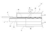
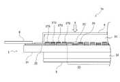
まず、放射線検出器の第1の実施形態について説明する。図1は、本発明の第1の実施形態に係る放射線検出器1aの構成例を模式的に示す断面図である。図1においては、図中の上側が、放射線線画像の撮影の際に放射線を入射させる側(放射線の上流側)である。図中の矢印Xは、放射線検出器1aに入射させる放射線を示す。図2は、第1の実施形態に係る放射線検出器1aの構成例を模式的に示す平面図である。なお、図2においては、説明のため、保護シート4を省略してある。<Radiation detector>
First, the first embodiment of the radiation detector will be described. FIG. 1 is a cross-sectional view schematically showing a configuration example of the
第1の実施形態に係る放射線検出器1aは、センサパネル2と、第1のシンチレータ31と、第2のシンチレータ32と、保護シート4と、基台5とを有する。そして、図1に示すように、センサパネル2の一方(入射させる放射線Xの上流側)の表面に第1のシンチレータ31が重ねて配置され、さらに第1のシンチレータ31を覆う保護シート4が配置される。また、センサパネル2の前記一方とは反対側の表面(入射させる放射線Xの下流側の表面)には、第2のシンチレータ32が配置される。第2のシンチレータ32は、基台5により支持される。 The
センサパネル2は、無アルカリガラスなどのガラス基板21と、このガラス基板21に二次元状に配置される複数の光電変換素子部23,24を有する。複数の光電変換素子部23,24には、第1の光電変換素子部23と第2の光電変換素子部24とが含まれる。第1の光電変換素子部23は、第1のシンチレータ31が発する光を受光して電気信号に変換する(受光した光に応じた電気信号を生成する)。第2の光電変換素子部24は、第2のシンチレータ32が発する光を受光して電気信号に変換する。なお、第1の光電変換素子部23と第2の光電変換素子部24の構成例については後述する。また、センサパネル2において、複数の光電変換素子部(第1の光電変換素子部23と第2の光電変換素子部24)が二次元状に配置される領域を「有効画素領域22」と称する。有効画素領域22は、入射した放射線Xを電気信号に変換できる領域である。 The
また、センサパネル2には配線25が設けられる。センサパネル2の有効画素領域22の外側に設けられる配線25には、例えば、第1の光電変換素子部23や第2の光電変換素子部24を駆動する信号を伝送する駆動線と、第1の光電変換素子部23や第2の光電変換素子部24が変換した(生成した)電気信号を読み出す信号線が含まれる。本発明の実施形態では、第1の光電変換素子部23と第2の光電変換素子部24と前記の配線25は、ガラス基板21の一方の表面であって第1のシンチレータ31の側の表面に設けられているものとする。なお、センサパネル2に設けられる配線25の種類や具体的な構成は特に限定されるものではない。また、センサパネル2の周縁部には、放射線検出器1aの外部との間で信号の送受信を行うための接続部6が接合される。接続部6には、例えばFPCなどが適用され、センサパネル2に設けられる配線25と外部の機器や回路基板などとを電気的に接続する。なお、接続部6の構成は特に限定されるものではない。 Further, the
第1のシンチレータ31と第2のシンチレータ32は、それぞれ、放射線Xが入射すると励起して光(可視光)を発する。第1のシンチレータ31と第2のシンチレータ32は、センサパネル2の表面に直角な方向視(以下、「平面視」と称する)において、少なくとも有効画素領域22の全域に重なるように設けられる。すなわち、図2に示すように、平面視において、第1のシンチレータ31の外周(輪郭)は、有効画素領域22の外周の外側に位置している。第2のシンチレータ32も同様である。なお、第1のシンチレータ31と第2のシンチレータ32の具体的な構成(材質や形成方法など)は特に限定されるものではなく、従来公知の各種の構成が適用できる。 The
保護シート4は、第1のシンチレータ31を保護する機能を有し、第1のシンチレータ31を覆うように、第1のシンチレータ31に重ねて配置される。なお、保護シート4の構成は特に限定されるものではない。第1のシンチレータ31が水分によって劣化などする材料から形成されるのであれば、第1のシンチレータ31を水分から保護するために遮水性を有することが好ましい。基台5は、第2のシンチレータ32を支持する部材である。基台5の構成は特に限定されるものではない。 The
センサパネル2の有効画素領域22の外側には遮光部26が配置される。遮光部26は、センサパネル2の有効画素領域22の外側において、第1のシンチレータ31が発する光が第2のシンチレータ32に入射することを防止する。図2に示すように、遮光部26は、平面視において、有効画素領域22の外側に、有効画素領域22を囲むように配置される。第1の実施形態では、遮光部26は、平面視において、有効画素領域22の外周(輪郭)から第1のシンチレータ31の外周までの範囲に配置される。このため、第1のシンチレータ31は、有効画素領域22の外側において遮光部26と重なる構成となる。特に、第1のシンチレータ31の有効画素領域22の外側に位置する部分の全体が遮光部26と重なる構成であることが好ましい。なお、遮光部26は、この範囲の全域に隙間なく配置され、切れ目や孔などが存在しない構成であることが好ましい。 A light-shielding
また、遮光部26は、センサパネル2と第1のシンチレータ31と第2のシンチレータ32の積層方向に関しては、第1のシンチレータ31と第2のシンチレータ32の間に配置される。第1の実施形態では、図1に示すように、遮光部26は、センサパネル2に設けられる配線25に重ねて配置される。換言すると、配線25と第1のシンチレータ31との間に配置される。なお、配線25と遮光部26は直接重なる(直接接触する)のではなく、それらの間に樹脂などの図略の絶縁層(例えば、平坦化膜)が介在している構成が適用できる。 Further, the light-shielding
遮光部26には、例えば、金属やカーボンブラックや樹脂材料などの膜が適用できる。ただし、遮光部26は遮光性を有していればよく、その材質(材料)は限定されるものではない。また、遮光部26は、後述する第2の光電変換素子部24の遮光層243と同じ材料からなる構成が適用できる。この場合、遮光部26は、第2の光電変換素子部24の遮光層243を形成する工程において、併せて形成される構成が適用できる。 For example, a film such as metal, carbon black, or a resin material can be applied to the light-shielding
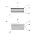
次に、有効画素領域22を構成する第1の光電変換素子部23と第2の光電変換素子部24の構成例について説明する。有効画素領域22は、例えば、同数またはほぼ同数の第1の光電変換素子部23と第2の光電変換素子部24とで構成される。そして、有効画素領域22において、複数の第1の光電変換素子部23と複数の第2の光電変換素子部24とは、例えば交互に並ぶように配置される。図3(a)は、第1の光電変換素子部23の構成例を模式的に示す断面図であり、図3(b)は、第2の光電変換素子部24の構成例を模式的に示す断面図である。図3(a)(b)においては、図中の上側が第1のシンチレータ31が配置される側(入射させる放射線Xの上流側)であり、下側がガラス基板21および第2のシンチレータ32が配置される側である。また、矢印Xは、撮影の際に入射させる放射線を示す。図3(a)(b)に示すように、第1の光電変換素子部23と第2の光電変換素子部24は、それぞれ、光透過層231,241と光電変換層232,242と遮光層233,243とを有する。 Next, a configuration example of the first photoelectric
光透過層231,241は、第1のシンチレータ31や第2のシンチレータ32が発する光を透過する層である。光透過層231,241には、例えば、ITO(酸化インジウムスズ)などの透明な金属化合物や、透明な樹脂材料が適用できる。ただし、光透過層231,241は、光透過性を有していればよく、具体的な材質や構成は特に限定されない。遮光層233,243は、第1のシンチレータ31や第2のシンチレータ32が発する光を遮光する層である。遮光層233,243には、例えば金属やカーボンブラックや樹脂材料などが適用できる。 The light transmitting layers 231 and 241 are layers that transmit light emitted by the
第1の光電変換素子部23の光電変換層232は、第1のシンチレータ31が発する光を電気信号に変換する(光に応じた電気信号を生成する)図略の光電変換素子が配置される層である。第2の光電変換素子部24の光電変換層242は、第2のシンチレータ32が発する光を電気信号に変換する(電気信号を生成する)図略の光電変換素子が配置される層である。第1の光電変換素子部23の光電変換層232と、第2の光電変換素子部24の光電変換層242は、同じ構成を有する。光電変換層232,242には、例えば、光が入射すると電気信号(電荷)を発生させるフォトダイオードなどの光電変換素子と、光電変換素子から電気信号を取り出すためのTFTなどのスイッチング素子が含まれる。さらに、光電変換層232,242には、スイッチング素子の駆動信号を伝送する駆動線と、光電変換素子から取り出した電気信号を伝送する信号線と、光電変換素子にバイアスを印加するためのバイアス線と、その他の所定の層(ゲート絶縁膜や平坦化膜)が含まれる。光電変換層232,242は、フォトエッチングプロセスを繰り返して光電変換素子やスイッチング素子や配線などを形成していくことで形成される。なお、光電変換層232,242の具体的な構成は特に限定されるものではなく、公知の各種放射線検出パネルと同じ構成が適用できる。 The
第1の光電変換素子部23は、図3(a)に示すように、第2のシンチレータ32に近い側(図3(a)においては下側)から、遮光層233、光電変換層232、光透過層231の順に重ねて配置される構成を有する。一方、第2の光電変換素子部24は、図3(b)に示すように、第2のシンチレータ32に近い側(図3(b)においては下側)から、光透過層241、光電変換層242、遮光層243の順に重ねて配置される構成を有する。すなわち、第1の光電変換素子部23においては、第1のシンチレータ31に近い側に光透過層231が配置され、第2のシンチレータ32に近い側に遮光層233が配置され、それらの間に光電変換層232が配置される。一方、第2の光電変換素子部24においては、第1のシンチレータ31に近い側に遮光層243が配置され、第2のシンチレータ32に近い側に光透過層241が配置され、それらの間に光電変換層242が配置される。 As shown in FIG. 3A, the first photoelectric
このような構成であると、第1のシンチレータ31が発する光は、第1の光電変換素子部23の光透過層231を透過して第1の光電変換素子部23の光電変換層232に入射する。一方、第2のシンチレータ32が発する光は、第1の光電変換素子部23の遮光層233により遮光されるため、第1の光電変換素子部23の光電変換層232には入射しない。したがって、第1の光電変換素子部23は、第1のシンチレータ31が発する光を受光(検出)して電気信号に変換する。 With such a configuration, the light emitted by the
また、第1のシンチレータ31が発する光は、第2の光電変換素子部24の遮光層243により遮光されるため、第2の光電変換素子部24の光電変換層242には入射しない。一方、第2のシンチレータ32が発する光は、第2の光電変換素子部24の光透過層241を透過して第2の光電変換素子部24の光電変換層242に入射する。したがって、第2の光電変換素子部24は、第2のシンチレータ32が発する光を受光(検出)して電気信号に変換する。 Further, since the light emitted by the
放射線検出器1aを用いて放射線画像を撮影する際には、第1のシンチレータ31の側から放射線Xを入射させる。放射線Xに含まれる周波数が低い低エネルギー成分(軟放射線)は物体を透過しにくく、周波数の高い高エネルギー成分(硬放射線)は物体を透過しやすい。このため、放射線Xが第1のシンチレータ31の側から入射すると、放射線Xの低エネルギー成分が第1のシンチレータ31において光に変換される。そして、変換された光は第1の光電変換素子部23の光電変換層232において電気信号に変換される。放射線Xの高エネルギー成分は、第1のシンチレータ31とセンサパネル2を透過して第2のシンチレータ32に入射する。そして、放射線Xの高エネルギー成分は第2のシンチレータ32において光に変換され、第2の光電変換素子部24の光電変換層232において電気信号に変換される。ただし、低エネルギー成分は、第1のシンチレータ31やセンサパネル2で吸収されて第2のシンチレータ32に到達しない。このため、第2の光電変換素子部24により変換された電気信号には、放射線Xの低エネルギー成分の情報は混入しない。 When taking a radiation image using the
このように、放射線検出器1aを用いた放射線画像の撮影時においては、放射線Xを第1のシンチレータ31の側から入射させる。これにより、第1の光電変換素子部23により放射線Xの低エネルギー成分を検出して低エネルギー成分の放射線画像を生成でき、第2の光電変換素子部24により放射線Xの高エネルギー成分を検出して高エネルギー成分の放射線画像を生成できる。すなわち、放射線検出器1aは、1回の放射線曝射により、エネルギー成分が互いに異なる2つの放射線画像を生成できる。 As described above, when the radiation image is taken by the
そして、遮光部26により、高エネルギー成分の放射線画像に低エネルギー成分の情報が混在することが防止される。すなわち、遮光部26が配置されない構成では、有効画素領域22の外側において第1のシンチレータ31が発する光は、第2のシンチレータ32に入射し、第2のシンチレータ32と基台5の界面などで反射して第2の光電変換素子部24の光電変換層242に入射する。その結果、特に有効画素領域22の外周に近い領域において、高エネルギー成分の放射線画像に低エネルギー成分の情報が混入する。混入した低エネルギー成分の情報はノイズとなり、物体の弁別の精度を低下させることがある。 Then, the light-shielding
これに対して、本発明の第1の実施形態によれば、遮光部26により、有効画素領域22の外側において、第1のシンチレータ31が発する光が第2のシンチレータ32に入射することが防止される。このため、高エネルギー成分の放射線画像に低エネルギー成分の情報が混入することを防止でき、高エネルギー成分の放射線画像にノイズが混入することを防止できる。 On the other hand, according to the first embodiment of the present invention, the light-shielding
次に、センサパネル2の製造方法および遮光部26の形成方法について説明する。まず、ガラス基板21の一方の表面に、第1の光電変換素子部23の遮光層233を形成し、第2の光電変換素子部24の光透過層241を形成する。遮光層233の形成方法や光透過層241の形成方法は特に限定されるものではなく、公知の各種の成膜方法が適用できる。また、第1の光電変換素子部23の遮光層233と第2の光電変換素子部24の光透過層241の形成の順序も特に限定されない。 Next, a method of manufacturing the
第1の光電変換素子部23の遮光層233と第2の光電変換素子部24の光透過層241を形成した後、それらのそれぞれの表面に、光電変換層232,242を形成する。光電変換層232,242は、例えばフォトエッチングプロセスを繰り返すことにより、光電変換素子やスイッチング素子や絶縁膜などを形成していくことで形成される。また、光電変換層232,242を形成する工程において、併せて、有効画素領域22の外側に、前記の配線25(信号線や駆動線)が形成される。なお、光電変換層232,242や配線25の形成方法は特に限定されるものではなく、公知の方法が適用できる。 After forming the light-
そして、第1の光電変換素子部23の光電変換層232の表面に光透過層231を重ねて形成し、第2の光電変換素子部24の光電変換層242の表面に遮光層243を重ねて形成する。遮光層243の形成方法や光透過層231の形成方法は特に限定されるものではなく、公知の各種の成膜方法が適用できる。また、第1の光電変換素子部23の光透過層231と第2の光電変換素子部24の遮光層243の形成の順序も特に限定されない。そして、第2の光電変換素子部24の光電変換層242の表面に遮光層243を重ねて形成する工程において、併せて、有効画素領域22の外側に遮光部26を形成する。これにより、有効画素領域22の外側には、遮光部26が、第2の光電変換素子部24の遮光層243と同じ材料により同じ工程で形成される。また、このような構成によれば、遮光部26を、有効画素領域22の外側に設けられる配線25に重ねて配置できる。このため、遮光部26を、センサパネル2の配線25と第1のシンチレータ31の間に配置できる。 Then, the
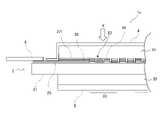
次に、第2の実施形態に係る放射線検出器1bについて説明する。前記第1の実施形態では、遮光部26が、有効画素領域22の外側において第1のシンチレータ31と重なる範囲に配置される構成を示したが、遮光部26の構成は、第1の実施形態に示す構成に限定されない。図4(a)は、第2の実施形態に係る放射線検出器1bの構成例を模式的に示す断面図である。図4(b)は、第2の実施形態に係る放射線検出器1bの構成例を模式的に示す平面図である。なお、図4(b)においては、保護シート4を省略してある。また、第1の実施形態と共通の構成には、第1の実施形態と同じ符号を付し、説明を省略する。図4(a)(b)に示すように、第2の実施形態に係る放射線検出器1bにおいては、遮光部26が、有効画素領域22を囲むように、センサパネル2の外周の縁まで設けられる。換言すると、平面視において、有効画素領域22の外周(輪郭)とガラス基板21の外周の縁との間の範囲に設けられる。ただし、遮光部26は、接続部6を避けて設けられる。このような構成であっても、第1の実施形態と同様の効果を奏することができる。なお、遮光部26の形成方法は、第1の実施形態と同じでよい。 Next, the
図5は、第3の実施形態に係る放射線検出器1cの構成例を模式的に示す断面図である。図5に示すように、有効画素領域22の外側には、センサパネル2の配線25に重ねて遮光部26が配置され、さらに遮光部26に重ねて第1の光反射防止部271が配置される。第1の光反射防止部271は、光の反射率が低い層である。また、第1の光反射防止部271は、光の透過率も低い。すなわち、第1の光反射防止部271は、第1のシンチレータ31が発する光を反射や透過せずに吸収する構成であることが好ましい。このような構成であると、第1のシンチレータ31が発する光が遮光部26に到達して反射することが防止または抑制される。このため、遮光部26で反射した光に起因するノイズを防止できる。特に、遮光部26が金属などからなり光の反射率が高い場合に、第1の光反射防止部271が配置される構成であることが好ましい。第1の光反射防止部271の材質は特に限定されるものではないが、例えばカーボンブラックや、黒色に着色された樹脂などが適用できる。なお、第1の光反射防止部271の具体的な材質(材料)は特に限定されるものではないが、遮光部26よりも光の反射率が低い材料からなることが好ましい。 FIG. 5 is a cross-sectional view schematically showing a configuration example of the
なお、図5においては、遮光部26と光反射防止部271が第1の実施形態の遮光部26と同じ範囲に配置される構成を示したが、第2の実施形態の遮光部26と同じ範囲に配置される構成であってもよい。 Note that FIG. 5 shows a configuration in which the light-shielding
次に、本発明の第4の実施形態に係る放射線検出器1dの構成例について説明する。図6は、本発明の第4の実施形態に係る放射線検出器1dの構成例を模式的に示す断面図である。第4の実施形態に係る放射線検出器1dには、有効画素領域22の外側において、第1のシンチレータ31と保護シート4の間に第2の光反射防止部272が配置される。第2の光反射防止部272は、光の反射率が低い層である。特に、保護シート4よりも光の反射率が低い構成が適用される。このような構成によれば、第1のシンチレータ31が発する光が有効画素領域22の外側において保護シート4で反射して第1の光電変換素子部23の光電変換層232に入射することが防止される。このため、保護シート4における光の反射に起因するノイズを防止できる。なお、第2の光反射防止部272の材質は特に限定されるものではなく、例えば第1の光反射防止部271と同様に、カーボンブラックや黒色に着色された樹脂材料などが適用できる。また、第2の光反射防止部272は、平面視において、有効画素領域22の外側の全域に、隙間なく配置される構成であることが好ましい。 Next, a configuration example of the
次に、本発明の第5の実施形態に係る放射線検出器1eの構成例について説明する。図7は、本発明の第5の実施形態に係る放射線検出器1eの構成例を模式的に示す断面図である。第5の実施形態に係る放射線検出器1eには、有効画素領域22の外側に、複数の第3の光電変換素子部273が配置される。第3の光電変換素子部273は、放射線画像の撮影において画像情報の取得には用いられない。第3の光電変換素子部273には、第2の光電変換素子部24と同じ構成が適用できる。すなわち、第3の光電変換素子部273の光電変換層242の第1のシンチレータ31の側には、遮光層243が設けられる。また、第3の光電変換素子部273は、第1のシンチレータ31の側と第2のシンチレータ32の側の両方に遮光層が配置され、遮光層どうしの間に光電変換層が配置される構成であってもよい。このような構成であれば、第3の光電変換素子部273が、第1の実施形態の遮光部26と同様の機能を有する。したがって、第1の実施形態と同様の効果を奏することができる。 Next, a configuration example of the
なお、第3の光電変換素子部273は、平面視において、有効画素領域22の外周から第1のシンチレータ31の外周までの範囲の全域にわたって配置される構成でなくてもよく、この範囲の一部に配置される構成であってもよい。この場合、第3の光電変換素子部273が配置される領域以外の領域には、第1の実施形態や第2の実施形態と同じ構成の遮光部26が配置される構成が適用できる。このように、第3の光電変換素子部273は、遮光部26の少なくとも一部を構成すればよい。例えば、平面視において、有効画素領域22の外側を囲むように複数の第3の光電変換素子部273が配置され、さらにその外側に、第1の実施形態や第2の実施形態と同じ遮光部26が配置される構成が適用できる。このような構成であっても、第1の実施形態と同様の効果を奏することができる。 The third photoelectric
また、第5の実施形態においては、第3の実施形態と同様に、第1の光反射防止部271が、第3の光電変換素子部273の遮光層243に重ねて配置されてもよい。さらに、第4の実施形態と同様に、有効画素領域22の外側において、第1のシンチレータ31と保護シート4の間に、第2の光反射防止部272が配置されてもよい。 Further, in the fifth embodiment, as in the third embodiment, the first light
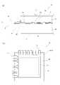
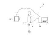
<放射線検出システム>
次に、放射線検出システム9の実施形態について説明する。図8は、本発明の実施形態に係る放射線検出システム9の構成例を模式的に示す図である。図8に示すように、放射線検出システム9は、放射線発生装置91と放射線検出装置92と制御・演算処理部93を有する。放射線発生装置91は、制御・演算処理部93による制御にしたがって放射線を曝射する。放射線発生装置91の構成は特に限定されるものではなく、公知の各種の放射線発生装置が適用できる。放射線検出装置92は、制御・演算処理部93による制御に従い、放射線発生装置91から曝射されて被写体である被検者Pを透過した放射線を検出し、放射線画像を生成して制御・演算処理部93に出力する。制御・演算処理部93は、放射線検出装置92から取得した放射線画像に対して所定の演算処理を行う。これにより、放射線検出システム9の使用者等は、被検者Pの診断を行うことができる。<Radiation detection system>
Next, an embodiment of the
放射線検出装置92には、前記の本発明の実施形態に係る放射線検出器1a,1b,1c,1d,1eが適用される。例えば、放射線検出装置92は、放射線検出器1a,1b,1c,1d,1eと、放射線検出器1a,1b,1c,1d,1eの駆動用の電力の供給源となるバッテリとを有し、これらが筐体に収容されている。制御・演算処理部93は、例えば、CPUとROMとRAMと有するコンピュータが適用できる。この場合、ROMには放射線発生装置91と放射線検出装置92を制御するコンピュータプログラムがあらかじめ格納されている。そして、CPUは、ROMに格納されているコンピュータプログラムを読み出し、RAMに展開して実行する。これにより、制御・演算処理部93は、放射線発生装置91や放射線検出装置92を制御する制御手段として機能する。、また、制御・演算処理部93は、放射線検出装置92から取得した放射線画像(画像信号)に対して所定の演算処理を実行する信号処理手段として機能する。 The
また、本発明の実施形態に係る放射線検出システム9は、1回の放射線曝射によってエネルギー成分が異なる2枚の放射線画像を取得することができる(ワンショットエネルギサブトラクション法)。具体的には、制御・演算処理部93は、放射線発生装置91を制御して被検者P(被写体)に向けて放射線を1回曝射する。そして、放射線検出装置92は、第1の光電変換素子部23により放射線Xの低エネルギー成分を検出して低エネルギー成分の画像を生成し、第2の光電変換素子部24により放射線Xの高エネルギー成分を検出して高エネルギー成分の画像を生成する。制御・演算処理部93は信号処理手段として機能し、放射線検出装置92が生成した高エネルギー成分の放射線画像と低エネルギー成分の放射線画像を取得し、取得した高エネルギー成分の放射線画像と低エネルギー成分の放射線画像の差分する演算処理を行う。これにより、制御・演算処理部93は、例えば硬部組織と軟部組織の一方を強調し他方を除去した画像(「エネルギーサブトラクション画像」と称する)を得ることができる。このように、本発明の実施形態に係る放射線検出システム9は、1回の放射線曝射において取得した複数の放射線画像(低エネルギー成分の放射線画像と高エネルギー成分の放射線画像)から、新たな放射線画像(エネルギーサブトラクション画像)を生成できる。 Further, the
なお、エネルギーサブトラクション画像を生成する処理は、放射線検出装置92が実行してもよい。例えば、放射線検出装置92において、放射線検出器1a,1b,1c,1d,1eには、接続部6を介して、CPUとROMとRAMを有するコンピュータが接続される。このコンピュータのROMには、放射線検出器1a,1b,1c,1d,1eの制御や、エネルギーサブトラクション画像を生成する処理を実行するためのコンピュータプログラムがあらかじめ格納されている。そして、CPUは、ROMに格納されているコンピュータプログラムを読み出し、RAMに展開して実行する。これにより、このコンピュータは、放射線検出器1a,1b,1c,1d,1eの制御手段として機能し、制御・演算処理部93からの指示に従い放射線検出器1a,1b,1c,1d,1eを制御する。また、このコンピュータは、1回の放射線曝射において取得した複数の放射線画像から新たな放射線画像を生成する処理を実行する演算処理手段として機能する。これにより、放射線検出装置92において、エネルギーサブトラクション画像が生成される。 The
以上、本発明の実施形態について詳細に説明したが、前記実施形態は、本発明を実施するにあたっての具体例を示したに過ぎない。本発明の技術的範囲は、前記実施形態に限定されるものではない。本発明は、その趣旨を逸脱しない範囲において種々の変更が可能であり、それらも本発明の技術的範囲に含まれる。 Although the embodiments of the present invention have been described in detail above, the above-described embodiments merely show specific examples for carrying out the present invention. The technical scope of the present invention is not limited to the above-described embodiment. The present invention can be modified in various ways without departing from the spirit of the present invention, and these are also included in the technical scope of the present invention.
(その他の実施例)
本発明は、上述の実施形態の1以上の機能を実現するプログラムを、ネットワーク又は記憶媒体を介してシステム又は装置に供給し、そのシステム又は装置のコンピュータにおける1つ以上のプロセッサーがプログラムを読出し実行する処理でも実現可能である。また、1以上の機能を実現する回路(例えば、ASIC)によっても実現可能である。(Other examples)
The present invention supplies a program that realizes one or more functions of the above-described embodiment to a system or device via a network or storage medium, and one or more processors in the computer of the system or device reads and executes the program. It can also be realized by the processing to be performed. It can also be realized by a circuit (for example, ASIC) that realizes one or more functions.
本発明は、放射線検出装置および放射線検出システムに好適な技術である。そして、本発明によれば、互いに異なるエネルギー成分の放射線画像を撮影できる放射線検出器において、それぞれのエネルギー成分の放射線画像に異なるエネルギー成分の情報が混ざらないようにできる。 The present invention is a technique suitable for a radiation detection device and a radiation detection system. According to the present invention, in a radiation detector capable of capturing radiation images of different energy components, it is possible to prevent information on different energy components from being mixed in the radiation images of each energy component.
1a,1b,1c,1d,1e:放射線検出器、2:センサパネル、21:ガラス基板、22:有効画素領域、23:第1の光電変換素子部、231:第1の光電変換素子部の光透過層、232:第1の光電変換素子部の光電変換層、233:第1の光電変換素子部の遮光層、24:第2の光電変換素子部、241:第2の光電変換素子部の光透過層、242:第2の光電変換素子部の光電変換層、243:第2の光電変換素子部の遮光層、25:センサパネルの配線、26:遮光部、271:第1の光反射防止部、272:第2の光反射防止部、273:第3の光電変換素子部、31:第1のシンチレータ、32:第2のシンチレータ、4:保護シート、5:基台、6:接続部1a, 1b, 1c, 1d, 1e: Radiation detector 2: Sensor panel, 21: Glass substrate, 22: Effective pixel area, 23: First photoelectric conversion element section, 231: First photoelectric conversion element section Light transmission layer, 232: photoelectric conversion layer of the first photoelectric conversion element, 233: Light-shielding layer of the first photoelectric conversion element, 24: Second photoelectric conversion element, 241: Second photoelectric conversion element. 242: Photoelectric conversion layer of the second photoelectric conversion element, 243: Light-shielding layer of the second photoelectric conversion element, 25: Wiring of the sensor panel, 26: Light-shielding, 271: First light Anti-reflection unit, 272: Second light anti-reflection unit, 273: Third photoelectric conversion element unit, 31: First scintillator, 32: Second scintillator, 4: Protective sheet, 5: Base, 6: Connection
Claims (12)
Translated fromJapanese前記センサパネルの一方の表面に重ねて配置される第1のシンチレータと、
前記センサパネルの前記一方とは反対側の表面に重ねて配置される第2のシンチレータと、
を有し、
前記複数の光電変換素子部が配置される領域の外側には、前記第1のシンチレータと前記第2のシンチレータとの間に、遮光部が配置されることを特徴とする放射線検出器。A sensor panel having a plurality of photoelectric conversion elements arranged two-dimensionally, and
A first scintillator placed on one surface of the sensor panel and
A second scintillator placed on the surface of the sensor panel opposite to the one side, and a second scintillator.
Have,
A radiation detector characterized in that a light-shielding portion is arranged between the first scintillator and the second scintillator outside the region where the plurality of photoelectric conversion element portions are arranged.
前記遮光部は、前記複数の光電変換素子部が配置される領域の外周から前記第1のシンチレータの外周までの範囲に配置されることを特徴とする請求項1に記載の放射線検出器。In a direction perpendicular to the surface of the sensor panel, the outer circumference of the first scintillator is located outside the outer circumference of the region where the plurality of photoelectric conversion element portions are arranged.
The radiation detector according to claim 1, wherein the light-shielding portion is arranged in a range from the outer periphery of the region where the plurality of photoelectric conversion element portions are arranged to the outer periphery of the first scintillator.
前記他の複数の光電変換素子部は、遮光層を有し、
前記他の複数の光電変換素子部の前記遮光層は、前記遮光部の少なくとも一部であることを特徴とする請求項1から3のいずれか1項に記載の放射線検出器。In addition to the plurality of photoelectric conversion element portions, a plurality of photoelectric conversion elementportions are arranged outside the region of the sensor panel in which the plurality of photoelectric conversion element portions are arranged.
The other plurality of photoelectric conversion element portions have a light-shielding layer.
The radiation detector according to any one of claims 1 to 3, wherein the light-shielding layer of the other plurality of photoelectric conversion element portions is at least a part of the light-shielding portion.
前記遮光部は、前記遮光層と同じ材料により形成されることを特徴とする請求項1から4のいずれか1項に記載の放射線検出器。The plurality of photoelectric conversion element units include a photoelectric conversion layer that converts incident light into an electric signal, and a light-shielding layer that is arranged so as to be superimposed on the photoelectric conversion layer.
The radiation detector according to any one of claims 1 to 4, wherein the light-shielding portion is formed of the same material as the light-shielding layer.
前記第1のシンチレータは、前記センサパネルの前記複数の光電変換素子部が配置される側に重ねて配置され、
前記遮光部は、前記センサパネルと前記第1のシンチレータの間に配置されることを特徴とする請求項1から5のいずれか1項に記載の放射線検出器。The plurality of photoelectric conversion element portions are arranged on one surface of the substrate of the sensor panel.
The first scintillator is arranged so as to be overlapped on the side of the sensor panel on which the plurality of photoelectric conversion element portions are arranged.
The radiation detector according to any one of claims 1 to 5, wherein the light-shielding portion is arranged between the sensor panel and the first scintillator.
前記遮光部は、前記信号線の前記第1のシンチレータの側に重ねて配置されることを特徴とする請求項6に記載の放射線検出器。On the outside of the region where the plurality of photoelectric conversion element portions are arranged in the sensor panel, a signal line for extracting an electric signal from the plurality of photoelectric conversion element portions is located on the side where the plurality of photoelectric conversion element portions are arranged. Placed on the same side of the surface,
The radiation detector according to claim 6, wherein the light-shielding portion is arranged so as to be overlapped on the side of the first scintillator of the signal line.
前記第1のシンチレータが発する光を受光して電気信号に変換する第1の光電変換素子部と、前記第2のシンチレータが発する光を受光して電気信号に変換する第2の光電変換素子部とが含まれることを特徴とする請求項1から9のいずれか1項に記載の放射線検出器。The plurality of photoelectric conversion elements are included in the plurality of photoelectric conversion elements.
A first photoelectric conversion element unit that receives light emitted by the first scintillator and converts it into an electric signal, and a second photoelectric conversion element unit that receives light emitted by the second scintillator and converts it into an electric signal. The radiation detector according to any one of claims 1 to 9, wherein the radiation detector comprises.
前記第2の光電変換素子部は、前記第2のシンチレータが発する光を電気信号に変換する光電変換層と、前記光電変換層の前記第1のシンチレータの側に重ねて配置されて前記第1のシンチレータが発する光を遮光する遮光層とを有することを特徴とする請求項10に記載の放射線検出器。The first photoelectric conversion element unit is arranged so as to be overlapped with a photoelectric conversion layer that converts light emitted by the first scintillator into an electric signal and a side of the second scintillator of the photoelectric conversion layer. It has a light-shielding layer that blocks the light emitted by the scintillator.
The second photoelectric conversion element unit is arranged so as to overlap with the photoelectric conversion layer that converts the light emitted by the second scintillator into an electric signal and the side of the first scintillator of the photoelectric conversion layer. The radiation detector according to claim 10, further comprising a light-shielding layer that blocks light emitted by the scintillator.
前記放射線検出器によって得られた電気信号を処理する信号処理手段と、
を有することを特徴とする放射線検出システム。The radiation detector according to any one of claims 1 to 11.
A signal processing means for processing an electric signal obtained by the radiation detector,
A radiation detection system characterized by having.
Priority Applications (4)
| Application Number | Priority Date | Filing Date | Title |
|---|---|---|---|
| JP2017176573AJP7057084B2 (en) | 2017-09-14 | 2017-09-14 | Radiation detector and radiation detection system |
| PCT/JP2018/033555WO2019054351A1 (en) | 2017-09-14 | 2018-09-11 | Radiation detector and radiation detecting system |
| CN201880073346.0ACN111356938B (en) | 2017-09-14 | 2018-09-11 | Radiation detector and radiation detection system |
| US16/816,911US11054531B2 (en) | 2017-09-14 | 2020-03-12 | Radiation detector and radiation detecting system |
Applications Claiming Priority (1)
| Application Number | Priority Date | Filing Date | Title |
|---|---|---|---|
| JP2017176573AJP7057084B2 (en) | 2017-09-14 | 2017-09-14 | Radiation detector and radiation detection system |
Publications (2)
| Publication Number | Publication Date |
|---|---|
| JP2019052907A JP2019052907A (en) | 2019-04-04 |
| JP7057084B2true JP7057084B2 (en) | 2022-04-19 |
Family
ID=65723925
Family Applications (1)
| Application Number | Title | Priority Date | Filing Date |
|---|---|---|---|
| JP2017176573AActiveJP7057084B2 (en) | 2017-09-14 | 2017-09-14 | Radiation detector and radiation detection system |
Country Status (4)
| Country | Link |
|---|---|
| US (1) | US11054531B2 (en) |
| JP (1) | JP7057084B2 (en) |
| CN (1) | CN111356938B (en) |
| WO (1) | WO2019054351A1 (en) |
Families Citing this family (4)
| Publication number | Priority date | Publication date | Assignee | Title |
|---|---|---|---|---|
| US12142164B2 (en)* | 2019-01-30 | 2024-11-12 | Sony Group Corporation | Encryption device and encryption method |
| CN112068178B (en)* | 2019-06-10 | 2023-08-29 | 睿生光电股份有限公司 | Radiation sensing apparatus |
| JP7199332B2 (en)* | 2019-10-07 | 2023-01-05 | キヤノン電子管デバイス株式会社 | Method for manufacturing radiation detection module |
| CN112713163A (en)* | 2020-12-30 | 2021-04-27 | 上海奕瑞光电子科技股份有限公司 | Dual-energy radiation flat panel detector, preparation method and detection system |
Citations (5)
| Publication number | Priority date | Publication date | Assignee | Title |
|---|---|---|---|---|
| JP2008516692A (en) | 2004-10-14 | 2008-05-22 | エクリン メディカル システムズ, インコーポレイテッド | Multicolor digital radiography detector with patterned mask for single exposure energy sensitive x-ray images |
| JP2012026932A (en) | 2010-07-26 | 2012-02-09 | Fujifilm Corp | Radiation detector |
| JP2012112928A (en) | 2010-05-31 | 2012-06-14 | Fujifilm Corp | Radiography equipment |
| JP2012233781A (en) | 2011-04-28 | 2012-11-29 | Fujifilm Corp | Radiation image detector and radiographic device |
| JP2016156719A (en) | 2015-02-25 | 2016-09-01 | 東芝電子管デバイス株式会社 | Radiation detector |
Family Cites Families (14)
| Publication number | Priority date | Publication date | Assignee | Title |
|---|---|---|---|---|
| EP1016881B1 (en)* | 1998-12-28 | 2005-12-21 | Kabushiki Kaisha Toshiba | Radiation detecting apparatus |
| JP5403848B2 (en)* | 2005-03-16 | 2014-01-29 | キヤノン株式会社 | Radiation detection apparatus and radiation detection system |
| US7569832B2 (en)* | 2006-07-14 | 2009-08-04 | Carestream Health, Inc. | Dual-screen digital radiographic imaging detector array |
| JP5004848B2 (en)* | 2007-04-18 | 2012-08-22 | キヤノン株式会社 | Radiation detection apparatus and radiation detection system |
| JP2010056396A (en) | 2008-08-29 | 2010-03-11 | Fujifilm Corp | X-ray detection element |
| US7956332B2 (en)* | 2008-10-29 | 2011-06-07 | General Electric Company | Multi-layer radiation detector assembly |
| US9075150B2 (en)* | 2009-07-30 | 2015-07-07 | Carestream Health, Inc. | Radiographic detector formed on scintillator |
| JP2011227044A (en)* | 2010-03-30 | 2011-11-10 | Fujifilm Corp | Radiation imaging device |
| CN103026261A (en)* | 2010-07-27 | 2013-04-03 | 富士胶片株式会社 | Radiation detector and manufacturing method for same |
| JP5117584B2 (en)* | 2011-01-25 | 2013-01-16 | 浜松ホトニクス株式会社 | Scintillator plate |
| KR20170042566A (en)* | 2014-08-08 | 2017-04-19 | 도레이 카부시키가이샤 | Method for manufacturing display member |
| JP6528387B2 (en)* | 2014-11-05 | 2019-06-12 | コニカミノルタ株式会社 | Scintillator panel and radiation detector |
| CN107045138B (en)* | 2017-06-20 | 2024-03-22 | 同方威视技术股份有限公司 | Back scattering detection module |
| JP2019152595A (en)* | 2018-03-06 | 2019-09-12 | 富士フイルム株式会社 | Radiation image detector |
- 2017
- 2017-09-14JPJP2017176573Apatent/JP7057084B2/enactiveActive
- 2018
- 2018-09-11CNCN201880073346.0Apatent/CN111356938B/enactiveActive
- 2018-09-11WOPCT/JP2018/033555patent/WO2019054351A1/ennot_activeCeased
- 2020
- 2020-03-12USUS16/816,911patent/US11054531B2/ennot_activeExpired - Fee Related
Patent Citations (5)
| Publication number | Priority date | Publication date | Assignee | Title |
|---|---|---|---|---|
| JP2008516692A (en) | 2004-10-14 | 2008-05-22 | エクリン メディカル システムズ, インコーポレイテッド | Multicolor digital radiography detector with patterned mask for single exposure energy sensitive x-ray images |
| JP2012112928A (en) | 2010-05-31 | 2012-06-14 | Fujifilm Corp | Radiography equipment |
| JP2012026932A (en) | 2010-07-26 | 2012-02-09 | Fujifilm Corp | Radiation detector |
| JP2012233781A (en) | 2011-04-28 | 2012-11-29 | Fujifilm Corp | Radiation image detector and radiographic device |
| JP2016156719A (en) | 2015-02-25 | 2016-09-01 | 東芝電子管デバイス株式会社 | Radiation detector |
Also Published As
| Publication number | Publication date |
|---|---|
| JP2019052907A (en) | 2019-04-04 |
| WO2019054351A1 (en) | 2019-03-21 |
| US11054531B2 (en) | 2021-07-06 |
| US20200209412A1 (en) | 2020-07-02 |
| CN111356938A (en) | 2020-06-30 |
| CN111356938B (en) | 2023-09-26 |
Similar Documents
| Publication | Publication Date | Title |
|---|---|---|
| JP7057084B2 (en) | Radiation detector and radiation detection system | |
| US11550069B2 (en) | Detector modules, detectors and medical imaging devices | |
| JP5693174B2 (en) | Radiation detection apparatus and radiation detection system | |
| CN108140125B (en) | Optical Fingerprint Imaging Systems and Area Array Sensors | |
| JP5642451B2 (en) | Portable radiography equipment set, portable radiography equipment | |
| JP5911274B2 (en) | Radiation detection apparatus and radiation imaging system | |
| JP5376897B2 (en) | Radiation imaging equipment | |
| TWI399860B (en) | Radiation photography device | |
| KR20110139186A (en) | X-ray imaging device | |
| KR101927690B1 (en) | Radiation imaging system | |
| CN115721326A (en) | Radiation imaging apparatus and radiation imaging system | |
| JP2007020679A (en) | Portable radiography system | |
| JP6245799B2 (en) | Radiation imaging apparatus and radiation imaging system | |
| JP6055167B2 (en) | Imaging device | |
| JP2018040582A (en) | Radiation detector | |
| JP2013072721A (en) | Radiation detector, radiation image capturing device, and program | |
| JP6472432B2 (en) | Radiation imaging system | |
| CN116598324A (en) | Sensor substrate and manufacturing method thereof, radiation imaging device and system | |
| JP2609590B2 (en) | 2D radiation detector | |
| JP6071986B2 (en) | Radiation imaging system | |
| JP2017067681A (en) | Radiation image imaging apparatus | |
| JP2012093208A (en) | Radiation imaging apparatus | |
| JP2010156646A (en) | X-ray inspection device | |
| JP2017058254A (en) | Radiation imaging apparatus and radiation imaging system | |
| JP2018080989A (en) | Radiation detector and radiation detection device |
Legal Events
| Date | Code | Title | Description |
|---|---|---|---|
| A621 | Written request for application examination | Free format text:JAPANESE INTERMEDIATE CODE: A621 Effective date:20200908 | |
| A131 | Notification of reasons for refusal | Free format text:JAPANESE INTERMEDIATE CODE: A131 Effective date:20210817 | |
| A521 | Request for written amendment filed | Free format text:JAPANESE INTERMEDIATE CODE: A523 Effective date:20211014 | |
| TRDD | Decision of grant or rejection written | ||
| A01 | Written decision to grant a patent or to grant a registration (utility model) | Free format text:JAPANESE INTERMEDIATE CODE: A01 Effective date:20220308 | |
| A61 | First payment of annual fees (during grant procedure) | Free format text:JAPANESE INTERMEDIATE CODE: A61 Effective date:20220407 | |
| R151 | Written notification of patent or utility model registration | Ref document number:7057084 Country of ref document:JP Free format text:JAPANESE INTERMEDIATE CODE: R151 |