JP7052464B2 - Manufacturing method of coreless substrate with fine wiring layer and manufacturing method of semiconductor package - Google Patents
Manufacturing method of coreless substrate with fine wiring layer and manufacturing method of semiconductor packageDownload PDFInfo
- Publication number
- JP7052464B2 JP7052464B2JP2018055036AJP2018055036AJP7052464B2JP 7052464 B2JP7052464 B2JP 7052464B2JP 2018055036 AJP2018055036 AJP 2018055036AJP 2018055036 AJP2018055036 AJP 2018055036AJP 7052464 B2JP7052464 B2JP 7052464B2
- Authority
- JP
- Japan
- Prior art keywords
- wiring layer
- fine wiring
- layer
- coreless substrate
- base material
- Prior art date
- Legal status (The legal status is an assumption and is not a legal conclusion. Google has not performed a legal analysis and makes no representation as to the accuracy of the status listed.)
- Active
Links
Images


Classifications
- H—ELECTRICITY
- H01—ELECTRIC ELEMENTS
- H01L—SEMICONDUCTOR DEVICES NOT COVERED BY CLASS H10
- H01L2224/00—Indexing scheme for arrangements for connecting or disconnecting semiconductor or solid-state bodies and methods related thereto as covered by H01L24/00
- H01L2224/01—Means for bonding being attached to, or being formed on, the surface to be connected, e.g. chip-to-package, die-attach, "first-level" interconnects; Manufacturing methods related thereto
- H01L2224/10—Bump connectors; Manufacturing methods related thereto
- H01L2224/15—Structure, shape, material or disposition of the bump connectors after the connecting process
- H01L2224/16—Structure, shape, material or disposition of the bump connectors after the connecting process of an individual bump connector
- H01L2224/161—Disposition
- H01L2224/16151—Disposition the bump connector connecting between a semiconductor or solid-state body and an item not being a semiconductor or solid-state body, e.g. chip-to-substrate, chip-to-passive
- H01L2224/16221—Disposition the bump connector connecting between a semiconductor or solid-state body and an item not being a semiconductor or solid-state body, e.g. chip-to-substrate, chip-to-passive the body and the item being stacked
- H01L2224/16225—Disposition the bump connector connecting between a semiconductor or solid-state body and an item not being a semiconductor or solid-state body, e.g. chip-to-substrate, chip-to-passive the body and the item being stacked the item being non-metallic, e.g. insulating substrate with or without metallisation
- H—ELECTRICITY
- H01—ELECTRIC ELEMENTS
- H01L—SEMICONDUCTOR DEVICES NOT COVERED BY CLASS H10
- H01L2224/00—Indexing scheme for arrangements for connecting or disconnecting semiconductor or solid-state bodies and methods related thereto as covered by H01L24/00
- H01L2224/73—Means for bonding being of different types provided for in two or more of groups H01L2224/10, H01L2224/18, H01L2224/26, H01L2224/34, H01L2224/42, H01L2224/50, H01L2224/63, H01L2224/71
- H01L2224/732—Location after the connecting process
- H01L2224/73201—Location after the connecting process on the same surface
- H01L2224/73203—Bump and layer connectors
- H01L2224/73204—Bump and layer connectors the bump connector being embedded into the layer connector
- H—ELECTRICITY
- H01—ELECTRIC ELEMENTS
- H01L—SEMICONDUCTOR DEVICES NOT COVERED BY CLASS H10
- H01L2924/00—Indexing scheme for arrangements or methods for connecting or disconnecting semiconductor or solid-state bodies as covered by H01L24/00
- H01L2924/15—Details of package parts other than the semiconductor or other solid state devices to be connected
- H01L2924/151—Die mounting substrate
- H01L2924/153—Connection portion
- H01L2924/1531—Connection portion the connection portion being formed only on the surface of the substrate opposite to the die mounting surface
- H01L2924/15311—Connection portion the connection portion being formed only on the surface of the substrate opposite to the die mounting surface being a ball array, e.g. BGA
Landscapes
- Production Of Multi-Layered Print Wiring Board (AREA)
- Combinations Of Printed Boards (AREA)
- Wire Bonding (AREA)
Description
Translated fromJapanese本発明は、微細配線層付きコアレス基板、半導体パッケージおよび半導体装置並びに微細配線層付きコアレス基板および半導体パッケージの製造方法に関する。 The present invention relates to a coreless substrate with a fine wiring layer, a semiconductor package and a semiconductor device, and a method for manufacturing a coreless substrate with a fine wiring layer and a semiconductor package.
半導体チップとマザーボード間の電気的接続のために半導体パッケージ基板が使用されている。また、半導体パッケージ基板には半導体チップと半導体パッケージが実装されるプリント配線板との熱膨張係数の相違の橋渡しを行い、システムの実装の接合信頼性を高める役割もある。このような役割から半導体パッケージ基板は、インターポーザ基板などと呼ばれる。
また、半導体パッケージ基板は、基板内の配線幅、ピッチを各層で変化させることで、半導体チップ、マザーボード相互の線幅、ピッチに変換し電気的接続を得ている。Semiconductor package substrates are used for electrical connections between semiconductor chips and motherboards. In addition, the semiconductor package substrate also has a role of bridging the difference in the coefficient of thermal expansion between the semiconductor chip and the printed wiring board on which the semiconductor package is mounted, and enhances the joining reliability of the system mounting. Because of this role, the semiconductor package substrate is called an interposer substrate or the like.
Further, the semiconductor package substrate is converted into the line width and pitch between the semiconductor chip and the motherboard by changing the wiring width and pitch in the substrate in each layer to obtain an electrical connection.
一方、半導体パッケージ基板と半導体チップの接続・実装方式は使用する状況により様々あるが半導体チップと半導体パッケージ基板をはんだや金等の金属接合で接続するフリップチップ接続・実装が多用されている。フリップチップ接続は半導体チップの端子面を基板側の端子面に配置することにより多くの端子を半導体パッケージ基板と接続できるため、高性能の半導体パッケージに多く用いられている。 On the other hand, there are various connection / mounting methods for the semiconductor package substrate and the semiconductor chip depending on the usage situation, but flip-chip connection / mounting for connecting the semiconductor chip and the semiconductor package substrate by metal bonding such as solder or gold is often used. Flip-chip connection is often used for high-performance semiconductor packages because many terminals can be connected to the semiconductor package substrate by arranging the terminal surface of the semiconductor chip on the terminal surface on the substrate side.
また、近年では高性能なシステムを短期間で開発するために従来のSoC(System on a Chip)だけでなく、1つのパッケージ上で大規模なシステムを構築するSiP(System in Package)が用いられている。例えば、CPU・GPUと大容量メモリ等の複数の半導体チップを1つのパッケージ基板上に隣同士に配置する場合やチップ同士をスタックし、3次元に配置する形態もある。 In recent years, not only the conventional SoC (System on a Chip) but also SiP (System in Package) that builds a large-scale system on one package has been used to develop a high-performance system in a short period of time. ing. For example, there are cases where multiple semiconductor chips such as CPU / GPU and large-capacity memory are arranged next to each other on one package board, or chips are stacked and arranged three-dimensionally.
また、2次元および3次元の少なくとも一方に複数の半導体チップを配置する形態においては、半導体パッケージ基板には数μm幅の微細配線や数十μmピッチのマイクロバンプの形成が求められている。これらの狭いバンプピッチの実装を実現するために、コア部に寸法安定性が高い材料を用いたインターポーザも提案されている。例えば、基板のコア部が半導体チップと材料が同じであるシリコンインターポーザや高い絶縁性を有し、半導体チップと線膨張係数が近いガラスインターポーザなどが提案されている。(参考文献1) Further, in a form in which a plurality of semiconductor chips are arranged in at least one of two dimensions and three dimensions, it is required to form fine wiring having a width of several μm and micro bumps having a pitch of several tens of μm on the semiconductor package substrate. In order to realize the mounting of these narrow bump pitches, an interposer using a material with high dimensional stability for the core portion has also been proposed. For example, a silicon interposer in which the core portion of the substrate is made of the same material as the semiconductor chip and a glass interposer having high insulating properties and having a linear expansion coefficient close to that of the semiconductor chip have been proposed. (Reference 1)
しかしながら、シリコンインターポーザにおいては半導体前工程用の設備を使用して製作するため、1枚のウエハから作製できるインターポーザに制限があることや製造設備も高価であるため、インターポーザのコストも高価となる。一方、ガラスインターポーザにおいても、コア部の貫通ビアの形成に専用の製造設備を要するため、同様に製造コストが高価となる。また、伝送特性においてもコア部の貫通ビア近辺での信号の劣化が問題となっている。これらの課題の解決策として、キャリア基材上に微細配線層を形成し、FCBGA(Flip Chip Ball Grid Array)用配線基板などと電極パッドを介して接合した後に、キャリア基材を除去し、半導体パッケージ基板上に微細配線層が形成される方式が考えられる。この方式では、コア部を有しないため、コア部での伝送特性の劣化を抑制することができる。また、剛直なキャリア基材上に微細配線層を形成するため、高精度で微細配線の形成、積層が可能となる。 However, since the silicon interposer is manufactured using the equipment for the semiconductor front-end process, the interposer that can be manufactured from one wafer is limited and the manufacturing equipment is expensive, so that the cost of the interposer is also high. On the other hand, also in the glass interposer, since a dedicated manufacturing facility is required for forming the penetrating via in the core portion, the manufacturing cost is similarly high. Further, in terms of transmission characteristics, deterioration of the signal in the vicinity of the penetrating via of the core portion has become a problem. As a solution to these problems, a fine wiring layer is formed on the carrier base material, and the wiring board for FCBGA (Flip Chip Ball Grid Array) is bonded to the carrier base material via an electrode pad, and then the carrier base material is removed to form a semiconductor. A method in which a fine wiring layer is formed on the package substrate can be considered. Since this method does not have a core portion, deterioration of transmission characteristics in the core portion can be suppressed. Further, since the fine wiring layer is formed on the rigid carrier base material, the fine wiring can be formed and laminated with high accuracy.
一方、FCBGA用配線基板のコア部の貫通ビア近辺での信号の劣化も懸念されている。その解決策としてコア部を有しない、いわゆるコアレス基板が提案されている。コアレス基板は貫通ビア付近でのインピーダンス不整合を抑制できるため、半導体パッケージ基板内での信号の劣化の改善が期待できる。そのため、コアレス基板上に上記微細配線層が形成できれば、微細配線層付きコアレス基板内の信号の劣化はより改善することが見込まれる。しかしながら、コアレス基板にキャリア基材付き微細配線層を実装する工程でのリフロー炉での加熱により、コアレス基板およびキャリア基材付き微細配線層に反りが発生する。そして、半導体パッケージ基板間の隣接するはんだ同士が離れ、接続のオープン不良が生じたり、逆にはんだが一体化することにより接続がショートの状態となる等の不具合が発生し、適切にはんだ接合ができない問題が生じるおそれがある。特にコアレス基板は絶縁樹脂層と金属配線層の積層体であるため、加熱時の基板の反り量はコア基材を有する半導体パッケージ基板よりも大きくなる。そのため、上記の接続不良が多発する。さらに、はんだ接合後の冷却時にキャリア基材付き微細配線層とコアレス基板の線膨張係数(CTE)の差の影響でコアレス基板全体が反り、はんだバンプに応力が発生し、はんだバンプに亀裂が生じるおそれもある。これらの影響により、製造の歩留まりやはんだ接合部の信頼性を十分に確保できないことが懸念される。 On the other hand, there is concern about signal deterioration in the vicinity of the penetrating via in the core portion of the FCBGA wiring board. As a solution, a so-called coreless substrate having no core portion has been proposed. Since the coreless substrate can suppress impedance mismatch in the vicinity of the through via, it can be expected to improve the deterioration of the signal in the semiconductor package substrate. Therefore, if the fine wiring layer can be formed on the coreless substrate, it is expected that the deterioration of the signal in the coreless substrate with the fine wiring layer will be further improved. However, due to heating in the reflow furnace in the process of mounting the fine wiring layer with a carrier base material on the coreless substrate, the coreless substrate and the fine wiring layer with a carrier base material are warped. Then, adjacent solders between the semiconductor package substrates are separated from each other, causing a connection failure, or conversely, the solders are integrated, resulting in a short-circuited connection. There may be problems that cannot be done. In particular, since the coreless substrate is a laminate of an insulating resin layer and a metal wiring layer, the amount of warpage of the substrate during heating is larger than that of a semiconductor package substrate having a core substrate. Therefore, the above-mentioned connection failure occurs frequently. Furthermore, during cooling after solder bonding, the entire coreless substrate warps due to the difference in the linear expansion coefficient (CTE) between the fine wiring layer with carrier substrate and the coreless substrate, stress is generated in the solder bumps, and cracks occur in the solder bumps. There is also a risk. Due to these influences, there is a concern that the manufacturing yield and the reliability of the solder joint cannot be sufficiently ensured.
また、キャリア基材付き微細配線層は、キャリア基材除去後には微細配線層上の半導体チップ搭載面に複数の半導体チップを搭載するため、キャリア基材付き微細配線層の面積は半導体チップよりも広くなる。そのため、従来の半導体チップを実装する場合よりも、キャリア基板端部の反りおよびはんだバンプに発生する応力が増大するため、上記のはんだ接合のオープン不良や、隣接するはんだの一体化による接続のショート状態、およびはんだバンプの亀裂が生じやすくなる。よって、半導体パッケージの接続信頼性の低下を及ぼすおそれがある。 Further, since the fine wiring layer with a carrier base material mounts a plurality of semiconductor chips on the semiconductor chip mounting surface on the fine wiring layer after the carrier base material is removed, the area of the fine wiring layer with a carrier base material is larger than that of the semiconductor chip. Become wider. Therefore, the stress generated in the warp of the end of the carrier board and the solder bumps increases as compared with the case of mounting a conventional semiconductor chip. The condition and cracks in the solder bumps are likely to occur. Therefore, there is a possibility that the connection reliability of the semiconductor package may be lowered.
また、コアレス基板にキャリア基材付き微細配線層を実装する際と同様に、微細配線層付きコアレス基板と半導体チップをはんだ接合するためにリフロー炉にて加熱する。この時にも微細配線層付きコアレス基板に反りが発生し、半導体チップと微細配線層間の隣接するはんだ同士が離れ、接続のオープン不良が生じたり、逆にはんだが一体化することにより接続がショートの状態となる等の不具合が発生し、適切にはんだ接合ができない問題が生じるおそれがある。さらに、はんだ接合後の冷却時に微細配線層付きコアレス基板と半導体チップの線膨張係数(CTE)の差の影響で半導体パッケージ全体が反り、はんだバンプに応力が発生し、はんだバンプに亀裂が生じるおそれもある。これらの影響により、製造の歩留まりやはんだ接合部の信頼性を十分に確保できないことが懸念される。これらの背景から、コアレス基板と微細配線層間および半導体チップと微細配線層間のはんだバンプの亀裂や電極パッドの剥離を防止し、配線の接続信頼性を確保することが必要となっている。 Further, as in the case of mounting the fine wiring layer with the carrier base material on the coreless substrate, the coreless substrate with the fine wiring layer and the semiconductor chip are heated in a reflow oven for solder bonding. At this time as well, the coreless board with the fine wiring layer is warped, and the adjacent solder between the semiconductor chip and the fine wiring layer is separated from each other, resulting in an open failure of the connection, or conversely, the solder is integrated and the connection is short-circuited. There is a possibility that problems such as a state may occur and a problem may occur in which solder bonding cannot be performed properly. Furthermore, during cooling after solder bonding, the entire semiconductor package may warp due to the difference in the coefficient of linear expansion (CTE) between the coreless substrate with a fine wiring layer and the semiconductor chip, causing stress on the solder bumps and causing cracks in the solder bumps. There is also. Due to these influences, there is a concern that the manufacturing yield and the reliability of the solder joint cannot be sufficiently ensured. Against this background, it is necessary to prevent cracks in the solder bumps between the coreless substrate and the fine wiring layer and between the semiconductor chip and the fine wiring, and to prevent the electrode pads from peeling off, thereby ensuring the wiring connection reliability.
本発明は、以上の事情の下になされ、微細配線層とコアレス基板との間並びに半導体チップと微細配線層付きコアレス基板のはんだバンプのオープンやショートの発生を抑制することができる微細配線層付きコアレス基板、半導体パッケージおよび半導体装置並びに微細配線層付きコアレス基板および半導体パッケージの製造方法を提供することを目的とする。 The present invention has been made under the above circumstances, and has a fine wiring layer capable of suppressing the opening and short circuit of solder bumps between the fine wiring layer and the coreless substrate and the semiconductor chip and the coreless substrate with the fine wiring layer. It is an object of the present invention to provide a coreless substrate, a semiconductor package and a semiconductor device, and a method for manufacturing a coreless substrate and a semiconductor package with a fine wiring layer.
本発明の一態様による微細配線層付きコアレス基板は、コア部がなく、ビルドアップ配線層からなるコアレス基板と、ビルドアップ配線層からなる微細配線層とを備え、前期微細配線層の配線パターン幅は上記コアレス基板の配線パターン幅よりも小さく、上記コアレス基板と上記微細配線層とは突起電極を介して電気的に接合されると共に、上記コアレス基板および上記微細配線層間の隙間に絶縁性の接着部材が充填され、上記微細配線層は、上記コアレス基板とは逆側の面にパッドを有することを特徴とする。 The coreless board with a fine wiring layer according to one aspect of the present invention includes a coreless board composed of a build-up wiring layer and a fine wiring layer composed of a build-up wiring layer without a core portion, and has a wiring pattern width of the previous period fine wiring layer. Is smaller than the wiring pattern width of the coreless substrate, and the coreless substrate and the fine wiring layer are electrically bonded via protrusion electrodes, and insulatingly adheres to the gap between the coreless substrate and the fine wiring layers. The member is filled, and the fine wiring layer is characterized by having a pad on a surface opposite to the coreless substrate.
また、本発明の一態様による半導体パッケージは、上記発明の一態様による微細配線層付きコアレス基板と、上記電極パッドを介して、上記微細配線層付きコアレス基板と接続している半導体素子と、上記微細配線層付きコアレス基板と上記半導体素子との間に挿入された接着部材を含むことを特徴とする。
また、本発明の一態様による半導体装置は、上記発明の一態様による半導体パッケージと、上記半導体パッケージの電極パッドを介して、上記半導体パッケージと接続されているプリント配線板を有することを特徴とする。Further, the semiconductor package according to one aspect of the present invention includes a coreless substrate with a fine wiring layer according to the above aspect, a semiconductor element connected to the coreless substrate with a fine wiring layer via the electrode pad, and the above. It is characterized by including an adhesive member inserted between a coreless substrate with a fine wiring layer and the semiconductor element.
Further, the semiconductor device according to one aspect of the present invention is characterized by having a semiconductor package according to one aspect of the present invention and a printed wiring board connected to the semiconductor package via an electrode pad of the semiconductor package. ..
また、本発明の一態様による微細配線層付きコアレス基板の製造方法は、キャリア基材上に剥離層を形成し、当該剥離層上に密着層を形成し、当該密着層上に銅箔層を形成し、銅箔層上に第一パッドおよびパターン配線形成し、絶縁樹脂を積層した微細配線層を形成し、当該微細配線層の上記剥離層とは逆側に第二パッドを形成してキャリア基材付き微細配線層を作製する工程と、上記キャリア基材付き微細配線層の上記第二パッド上に突起電極を形成する工程と、コアレス基板保持用キャリア基材上に剥離層を形成し、当該剥離層上に密着層を形成し、当該密着層上に上記コアレス基板を配置する工程と、上記キャリア基材付き微細配線層の第二パッドと上記コアレス基板のパッドを上記突起電極を介して接合する工程と、上記キャリア基材付き微細配線層と上記コアレス基板との隙間に絶縁性の接着部材を充填する工程と、上記キャリア基材を上記剥離層の位置でキャリア基材付き微細配線層から剥離し、上記第一パッドを微細配線層付きコアレス基板の上記第一パッドとして露出させる工程と、を備えることを特徴とする。 Further, in the method for manufacturing a coreless substrate with a fine wiring layer according to one aspect of the present invention, a release layer is formed on a carrier base material, an adhesion layer is formed on the release layer, and a copper foil layer is formed on the adhesion layer. A carrier is formed by forming a first pad and a pattern wiring on a copper foil layer, forming a fine wiring layer in which an insulating resin is laminated, and forming a second pad on the opposite side of the fine wiring layer to the peeling layer. A step of producing a fine wiring layer with a base material, a step of forming a protrusion electrode on the second pad of the fine wiring layer with a carrier base material, and a process of forming a release layer on the carrier base material for holding a coreless substrate. The step of forming an adhesion layer on the peeling layer and arranging the coreless substrate on the adhesion layer, and the second pad of the fine wiring layer with a carrier base material and the pad of the coreless substrate via the protrusion electrode. A step of joining, a step of filling a gap between the carrier base material-attached fine wiring layer and the coreless substrate with an insulating adhesive member, and a step of placing the carrier base material at the position of the carrier base material at the position of the carrier base material. It is characterized by comprising a step of peeling from the first pad and exposing the first pad as the first pad of a coreless substrate with a fine wiring layer.
さらに、また、本発明の一態様による半導体パッケージの製造方法は、上記本発明の一態様による微細配線層付きコアレス基板の第一パッド上に突起電極を形成する工程と、
上記微細配線層付きコアレス基板の第一パッドと上記半導体素子のパッドを上記突起電極を介して接合する工程と、上記微細配線層付きコアレス基板と上記半導体素子との隙間に絶縁性の接着部材を充填する工程と、上記コアレス基板保持用キャリア基材を上記剥離層の位置で微細配線層付きコアレス基板から剥離し、微細配線層付きコアレス基板の第三パッドとして露出させる工程と、を備えることを特徴とする。Furthermore, the method for manufacturing a semiconductor package according to one aspect of the present invention includes a step of forming a protruding electrode on a first pad of a coreless substrate with a fine wiring layer according to the above aspect of the present invention.
A step of joining the first pad of the coreless substrate with a fine wiring layer and the pad of the semiconductor element via the protrusion electrode, and an insulating adhesive member in the gap between the coreless substrate with the fine wiring layer and the semiconductor element. It is provided with a step of filling and a step of peeling the carrier base material for holding the coreless substrate from the coreless substrate with a fine wiring layer at the position of the peeling layer and exposing it as a third pad of the coreless substrate with a fine wiring layer. It is a feature.
本発明の一態様によると、コアレス基板をコアレス基板保持用キャリア基材上に形成することにより、キャリア基材付き微細配線層のコアレス基板への実装工程および半導体チップの微細配線層付きコアレス基板への実装工程において、冷却時のはんだバンプ部や電極パッドと絶縁樹脂界面に発生する応力が低減されるため、はんだバンプの亀裂や電極パッドおよび絶縁層の剥離の発生を抑制できる。 According to one aspect of the present invention, by forming the coreless substrate on the carrier substrate for holding the coreless substrate, the step of mounting the fine wiring layer with the carrier substrate on the coreless substrate and the coreless substrate with the fine wiring layer of the semiconductor chip can be obtained. In the mounting process, the stress generated at the solder bump portion and the interface between the electrode pad and the insulating resin during cooling is reduced, so that the occurrence of cracks in the solder bump and peeling of the electrode pad and the insulating layer can be suppressed.
以下、図面を参照しながら本発明の実施形態について説明する。
ここで、図面は模式的なものであり、厚みと平面寸法との関係、各層の厚みの比率等は現実のものとは異なることがある。また、以下に示す実施形態は、本発明の技術的思想を具体化するための構成を例示するものであって、本発明の技術的思想は、構成部品の材質、形状、構造等が下記のものに特定されるものではない。本発明の技術的思想は、特許請求の範囲に記載された請求項が規定する技術的範囲内において、種々の変更を加えることができる。Hereinafter, embodiments of the present invention will be described with reference to the drawings.
Here, the drawings are schematic, and the relationship between the thickness and the plane dimensions, the ratio of the thickness of each layer, and the like may differ from the actual ones. Further, the embodiments shown below exemplify a configuration for embodying the technical idea of the present invention, and the technical idea of the present invention describes the materials, shapes, structures, etc. of the constituent parts as follows. It is not specific to things. The technical idea of the present invention may be modified in various ways within the technical scope specified by the claims described in the claims.
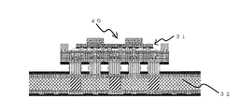
図1は本発明の一実施形態による半導体パッケージの構造を示す断面図である。図1に示すように、半導体パッケージ31は、本発明の一実施形態による微細配線層付きコアレス基板100(詳細は後述)と、微細配線層付きコアレス基板100の電極パッドを介して、微細配線層付きコアレス基板100と接続されている半導体チップ17と、微細配線層付きコアレス基板100と半導体チップ17との間に挿入されたアンダーフィル9bとを有している。 FIG. 1 is a cross-sectional view showing the structure of a semiconductor package according to an embodiment of the present invention. As shown in FIG. 1, the semiconductor package 31 is provided with a fine wiring layer via a
微細配線層付きコアレス基板100に設けられたコアレス基板101は、コア部がなく、配線パターン1および、絶縁樹脂2を積層したビルドアップ配線層26で形成されている。
ビルドアップ配線層26は、公知であるビルドアップ工法により形成され、絶縁樹脂2と配線パターン1とを有する。絶縁樹脂2の形成材料には、例えばエポキシ系、ポリイミド系樹脂が用いられ、樹脂にフィラーを添加した材料も用いることができる。また、配線パターン1の形成材料には、例えば銅を用いることができる。なお、ビルドアップ配線層26の各層の配線パターン1はビア3により相互に電気的に接続されている。The coreless substrate 101 provided on the
The build-up
最上層の配線パターン1には電気信号を外部との間で入出力するための電極パッド4が接続され、最下層の配線パターン1には電気信号を外部との間で入出力するための電極パッド7が接続されている。また、ビルドアップ配線層26の最表面には、ソルダーレジスト5が形成されている。ソルダーレジスト5は、電極パッド4上を開口するように形成する。なお、ソルダーレジスト5の形成材料は例えば、感光性エポキシ樹脂や樹脂にフィラーを添加した材料を用いることができる。また、公知であるコアレス基板の製造方法にはコアレス基板の片方の面のみにソルダーレジスト5が形成されている方法もあり、ソルダーレジスト5の形成方法・形態は特に限定されない。 An
電極パッド4上には、はんだバンプ6が形成されている。はんだバンプ6は、ソルダーレジスト5を形成した後に、電極パッド4上に印刷法やはんだボール振込み法などを用いて形成される。
コアレス基板101の半導体チップ搭載面側にビルドアップ配線層のみで形成された微細配線層200がはんだバンプ6などを介して金属接合されている。また、コアレス基板101と微細配線層200との隙間はアンダーフィル9aで埋め固められている。
また、微細配線層200の半導体チップ搭載面には、半導体チップ(半導体素子の一例)17がはんだバンプ10を介して接合されている。半導体チップ17と微細配線層200との隙間はアンダーフィル9bで埋め固められている。Solder bumps 6 are formed on the
A
Further, a semiconductor chip (an example of a semiconductor element) 17 is bonded to the semiconductor chip mounting surface of the
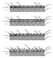
図2は、本発明の一実施形態によるキャリア基材付き微細配線層の構造を示す断面図である。
図2に示すように、キャリア基材付き微細配線層102は、キャリア基材11と、キャリア基材11上に形成された剥離層12と、剥離層12上に形成された密着層13と、密着層13上に形成された銅箔層14と、銅箔層14上に形成されたパターン配線および絶縁樹脂21を積層した微細配線層200とを有している。なお、微細配線層の配線パターン幅はコアレス基板の配線パターン幅よりも小さい。FIG. 2 is a cross-sectional view showing the structure of a fine wiring layer with a carrier substrate according to an embodiment of the present invention.
As shown in FIG. 2, the fine wiring layer 102 with a carrier base material includes a carrier base material 11, a release layer 12 formed on the carrier base material 11, and an
微細配線層200と半導体パッケージ基板101との接合を、平坦性を確保した上で行うために、キャリア基材11上に微細配線層200が形成されている。キャリア基材付き微細配線層102をコアレス基板101(図1参照)に実装した後に、キャリア基材付き微細配線層102を微細配線層200とキャリア基材11に分離するための剥離層12がキャリア基材11上に形成されている。 The
図3は、本発明の一実施による、キャリア基材付き微細配線層が実装された微細配線層付きコアレス基板の構造を示す断面図である。
図3に示すように、微細配線層付きコアレス基板100は、銅箔層上に形成されたパターン配線および絶縁樹脂を積層した微細配線層200と、微細配線層200の電極パッドを介して微細配線層200と接続しているコアレス基板101と、微細配線層200とコアレス基板101との間に挿入されたアンダーフィル9bとを有している。また、コアレス基板はコアレス基板保持用キャリア基材上に微細配線層が実装される面の反対の面と接するように配置されている。FIG. 3 is a cross-sectional view showing the structure of a coreless substrate with a fine wiring layer on which a fine wiring layer with a carrier base material is mounted according to one embodiment of the present invention.
As shown in FIG. 3, the
コアレス基板において、キャリア基材付き微細配線層102の搭載領域上にフラックスを塗布した後、キャリア基材付き微細配線層102をコアレス基板101上に実装する。その後、微細配線層200とコアレス基板101との隙間にアンダーフィル9aを挿入する。その後、キャリア基材付き微細配線層からキャリア基材を分離する。これによって、本実施形態による微細配線層付きコアレス基板100が形成される。 In the coreless substrate, after applying flux on the mounting region of the fine wiring layer 102 with a carrier base material, the fine wiring layer 102 with a carrier base material is mounted on the coreless substrate 101. After that, the underfill 9a is inserted into the gap between the
ここで、コアレス基板保持用キャリア基材上にコアレス基板を形成しない場合、実装工程において、加熱時にコアレス基板が反り、キャリア基材付き微細配線層とのはんだ接合が適切に行われず、コアレス基板とキャリア基材付き微細配線層の隣接するはんだ同士が離れ、接続のオープン不良が生じたり、逆にはんだが一体化することにより接続がショートの状態となるおそれがある。さらに、はんだ接合温度から常温に冷却される過程において、キャリア基材付き微細配線層102とコアレス基板101との線膨張係数(CTE)の差により、コアレス基板101とキャリア基材付き微細配線層102との間に応力が発生する。それにともない、コアレス基板101の反りおよびはんだバンプ6への応力が増加し、はんだバンプ6の亀裂や電極パッド4および微細配線層200の絶縁樹脂の剥離が発生するおそれがある。 Here, when the coreless substrate is not formed on the carrier substrate for holding the coreless substrate, the coreless substrate warps during heating in the mounting process, and solder bonding with the fine wiring layer with the carrier substrate is not properly performed. Adjacent solders of the fine wiring layer with a carrier base material may be separated from each other, causing a connection failure, or conversely, the solders may be integrated, resulting in a short connection. Further, in the process of cooling from the solder bonding temperature to room temperature, the difference in the coefficient of linear expansion (CTE) between the carrier-based fine wiring layer 102 and the coreless substrate 101 causes the coreless substrate 101 and the carrier-based fine wiring layer 102 to be cooled. Stress is generated between and. Along with this, the warp of the coreless substrate 101 and the stress on the solder bumps 6 increase, which may cause cracks in the solder bumps 6 and peeling of the insulating resin of the
一方、コアレス基板保持用キャリア基材上にコアレス基板を形成した場合、実装工程において、加熱時では剛直なキャリア基材にコアレス基板が配置されているため、コアレス基板の反りが抑制できるため、キャリア基材付き微細配線層とのはんだ接合が適切に実施することができる。さらに、キャリア基材付き微細配線層のキャリア基材とコアレス基板のコアレス基板保持用キャリア基材は同じ材質であり、冷却時のキャリア基材付き微細配線層102とコアレス基板101との線膨張係数(CTE)の差がより小さくなるため、半導体パッケージ51の反りおよびはんだバンプ6への応力が抑制され、はんだバンプ6の亀裂や電極パッド4および微細配線層200の絶縁樹脂の剥離の発生を抑制できる。 On the other hand, when the coreless substrate is formed on the carrier substrate for holding the coreless substrate, the coreless substrate is arranged on the carrier substrate which is rigid at the time of heating in the mounting process, so that the warp of the coreless substrate can be suppressed. Solder bonding with the fine wiring layer with a base material can be appropriately performed. Further, the carrier base material of the fine wiring layer with the carrier base material and the carrier base material for holding the coreless substrate of the coreless substrate are made of the same material, and the linear expansion coefficient between the fine wiring layer 102 with the carrier base material and the coreless substrate 101 during cooling is used. Since the difference in (CTE) becomes smaller, the warp of the semiconductor package 51 and the stress on the solder bumps 6 are suppressed, and the cracks of the solder bumps 6 and the peeling of the insulating resin of the
次に、コアレス基板101にスティフナ15を貼り合わせる。なお、スティフナ15の厚さは特に限定されず、高い剛性が確保できる厚さでよい。スティフナ15の形成材料には、半導体パッケージ51の線膨張係数および剛性の関係より選択し、例えば、鉄、銅、銅合金、ステンレス鋼などが用いられる。
スティフナ15とコアレス基板101とを密着させるために例えば、スティフナ15に接着層16を塗布し、コアレス基板101と密着させ、接着する。なお、接着層16の形成材料としては、エポキシ系およびアクリル系接着剤などがある。なお、スティフナ15を形成する工程は、キャリア基材付き微細配線層102を実装する前、半導体チップ17を実装する前およびプリント配線板32(図4参照)に実装前のどの工程の間でも構わない。Next, the
In order to bring the
その後、微細配線層付きコアレス基板101の半導体チップ17の搭載面に、はんだボール搭載法などではんだボールを搭載し、リフロー炉にて加熱することにより、微細配線層200にはんだバンプ10(図1参照)を形成する。その後、半導体チップ17を微細配線層付きコアレス基板100に実装する。 After that, the solder balls are mounted on the mounting surface of the
ここで、コアレス基板保持用キャリア基材上にコアレス基板を形成しているため、リフロー炉での加熱の際に微細配線層付きコアレス基板の反りを抑制することができるため、半導体チップ17とのはんだ接合がはんだのブリッジなどの不具合なく、適切に接合できる。さらに、コアレス基板保持用キャリア基材上に微細配線層付きコアレス基板が形成されているため、冷却時の半導体チップ17と微細配線層付きコアレス基板100との線膨張係数(CTE)の差は小さくなるため、半導体パッケージ31の反りおよびはんだバンプ10への応力が抑制され、はんだバンプ10の亀裂や接続パッド20および半導体チップ17の絶縁樹脂の剥離の発生を抑制できる。 Here, since the coreless substrate is formed on the carrier substrate for holding the coreless substrate, it is possible to suppress the warp of the coreless substrate with a fine wiring layer during heating in the reflow furnace. Solder joining can be done properly without any problems such as solder bridges. Further, since the coreless substrate with a fine wiring layer is formed on the carrier base material for holding the coreless substrate, the difference in linear expansion coefficient (CTE) between the
半導体チップ17と微細配線層200との隙間にアンダーフィル9bを挿入する。その後、コアレス基板保持用キャリア基材と微細配線層付きコアレス基板をキャリア基材付き微細配線層とキャリア基材を分離した方法と同様の方法で剥離する。
その後、微細配線層付きコアレス基板100のプリント配線板搭載面に、はんだボール搭載法などではんだボールを搭載し、リフロー炉にて加熱することにより、はんだバンプ8(図1参照)を形成する。このようにして、図1に示す半導体パッケージ31を作製する。
その後、半導体パッケージ31をプリント配線板32に実装し、図4に示すように、半導体パッケージ31と、半導体パッケージ31の電極パッド7を介して、半導体パッケージ31と接続されているプリント配線板32とを有する半導体装置40を作製する。The underfill 9b is inserted into the gap between the
After that, the solder balls are mounted on the printed wiring board mounting surface of the
After that, the semiconductor package 31 is mounted on the printed
以下に本発明の一実施形態による微細配線層付きコアレス基板の製造方法について説明するが、本発明はこれに限定されるわけではない。
<キャリア基材付き微細配線層の作製>
キャリア基材付き微細配線層102の作製について図5から図7を用いて説明する。キャリア基材11として、例えばガラス基板を用いる。ガラス基板は平坦性に優れており、微細配線層200の形成に適している。また、ガラス基板は低線膨張係数であるため、パターンの配置精度に優れており、コアレス基板101への実装の際に、微細配線層付きキャリア基材102をコアレス基板101に精度良く接合することができる。ガラス基板の厚さは作製時のガラス基板の反り発生を抑制する観点から厚いほうが好ましく、例えば0.7mm以上が好ましい。なお、キャリア基材11の材料はガラス基板に限定されず、表面が平滑であり、高弾性率で低線膨張係数である材料であれば良く、シリコン基板、メタル基板、セラミックス基板でも良い。Hereinafter, a method for manufacturing a coreless substrate with a fine wiring layer according to an embodiment of the present invention will be described, but the present invention is not limited thereto.
<Making a fine wiring layer with a carrier base material>
The production of the fine wiring layer 102 with a carrier base material will be described with reference to FIGS. 5 to 7. As the carrier base material 11, for example, a glass substrate is used. The glass substrate has excellent flatness and is suitable for forming the
次に、キャリア基材11上に微細配線層200を形成する。図5(a)に示すように、キャリア基材11の一方の面に、実装工程にてキャリア基材11を剥離するための剥離層12を形成する。剥離層12は紫外線を透過する厚さに調整しておく。
その後、図5(a)に示すように、剥離層上に紫外線で硬化する接着剤を塗布して密着層13を形成する。
次に、図5(b)に示すように、平坦な定盤18上に薄い銅箔層14を敷き、図5(c)に示すように、真空中で密着層13と銅箔層14とが接するように配置し、この状態で密着層13に紫外線を照射し、図6(a)に示すように、密着層13を硬化させ、定盤18を取り除く。銅箔層14は、定盤18の平坦性を保持した状態で硬化されるため、銅箔層14上に微細なパターンを形成することができる。Next, the
Then, as shown in FIG. 5A, an adhesive that is cured by ultraviolet rays is applied onto the release layer to form the
Next, as shown in FIG. 5 (b), a thin
次に、図6(b)に示すように、銅箔層14上にレジストパターン19をフォトリソグラフィ法などを用いて形成し、銅箔層14をシード層としてレジストパターン19に形成された複数の開口部に電解めっきにより半導体チップ17(図6では不図示)との接続パッド(パターン配線の一部)20を形成する。キャリア基材11を剥離し、接続パッド20を露出したときに、接続パッド20の表面がAuとなるように銅箔層14側からAu/Ni/Cuの順にめっきを形成する。これにより接続パッド20はAu/Ni/Cuの積層構造を有する。このとき、AuへのCu拡散を防止するため、銅箔層14とAuの間に薄いNiを形成してからAu/Ni/Cuのめっきを行う。その後、図6(c)に示すように、レジストパターン19を除去する。 Next, as shown in FIG. 6B, a plurality of resist
次に、図6(d)に示すように、接続パッド20上にスピンコート法を用いて絶縁樹脂21を形成する。絶縁樹脂の21の形成材料には、感光性エポキシ系樹脂が用いられる。絶縁樹脂21はスピンコート法ではなく、絶縁樹脂フィルムを真空ラミネーターで圧縮加熱により形成してもよい。 Next, as shown in FIG. 6D, the insulating resin 21 is formed on the
次に、図6(e)に示すように、接続パッド20に貫通ビア22を形成する。本実施例では絶縁樹脂21に感光性エポキシ系樹脂が用いられており、絶縁樹脂21に対して紫外線(UV)露光および現像を実施することにより、貫通ビア22を形成する。絶縁樹脂21に非感光性の樹脂が用いられている場合には、レーザー光照射により絶縁樹脂21に貫通ビアを形成しても良い。次に、アッシングなどで接続パッド上の残渣などを除去し、無電解めっき法およびスパッタリング法などを用いて電解めっきのシード層(不図示)を形成する。このシード層の形成材料は、無電解めっき法ではCuが適しており、スパッタリング法ではTi/CuおよびCr/Cuなどが適している。このシード層は電解めっき後のシード層エッチング工程で配線細りを抑制できるように、厚さが300nm以下程度となるように薄く形成することが望ましい。 Next, as shown in FIG. 6 (e), a penetrating via 22 is formed on the
次に、図6(f)に示すように、シード層上にレジストパターン19を形成し、レジストパターン19に形成された開口部に電解銅めっきで微細配線23を形成する。次に、図6(g)に示すように、レジストパターン19を除去し、微細配線23をマスクとして、シード層をエッチングする。図7(a)に示すように、以上の微細配線形成工程を積み重ねる配線層数に合わせて工程を繰り返し、微細配線層200を形成する。 Next, as shown in FIG. 6 (f), a resist
その後、図7(b)に示すように、コアレス基板101(図7(b)では不図示)の実装面側の微細配線層200の最表面に絶縁樹脂層24を形成する。絶縁樹脂層24は、感光性エポキシ系樹脂を用いて形成される。次に、図7(c)に示すように、UV露光および現像を実施し、微細配線200のパターン配線が露出される開口部25を絶縁樹脂層24に形成し、ベークにより絶縁樹脂層24を硬化する。 After that, as shown in FIG. 7B, the insulating resin layer 24 is formed on the outermost surface of the
露出したパターン配線のCuの酸化防止とはんだバンプの濡れ性を良くするため、パターン配線に表面処理を行う。パターン配線の表面にNi/Pd/Auからなるパッド表面処理層を形成する。なお、パターン配線の表面に、水溶性プレフラックス(Organic Sold erability Preservative:OSP) による表面処理によって有機被を形成しても良い。
次に、図7(d)に示すように、はんだバンプ(突起電極の一例)6をパッド表面処理層上に搭載し、リフローした後、キャリア基材11を個片化することでキャリア基材付き微細配線層102が完成する。Surface treatment is performed on the pattern wiring in order to prevent the Cu of the exposed pattern wiring from being oxidized and to improve the wettability of the solder bumps. A pad surface treatment layer made of Ni / Pd / Au is formed on the surface of the pattern wiring. An organic cover may be formed on the surface of the pattern wiring by surface treatment with a water-soluble preservative (OSP).
Next, as shown in FIG. 7 (d), a solder bump (an example of a protrusion electrode) 6 is mounted on a pad surface treatment layer, reflowed, and then the carrier base material 11 is separated into individual pieces to form a carrier base material. The fine wiring layer 102 with soldering is completed.
<コアレス基板の作製>
次に、コアレス基板の作製について説明する。ビルドアップ配線層の絶縁材料2としてフィラーを添加したエポキシ系樹脂を用い、配線の材料として銅を用いたビルドアップ配線層を6層、および最表面には電極パッド4、7上に開口するようにソルダーレジスト5が形成されたコアレス基板を公知の技術を用いて作製する。また、キャリア基材付き微細配線層との接合面のパッド上に、はんだボール搭載法により、はんだバンプを形成する。このようにしてコアレス基板101を作製する。<Manufacturing of coreless substrate>
Next, the production of the coreless substrate will be described. Epoxy resin with filler added is used as the insulating
次に、コアレス基板保持用キャリア基材27上にコアレス基板101を配置する。コアレス基板保持用キャリア基材27として、例えばガラス基板を用いる。ガラス基板は平坦性に優れており、コアレス基板に平坦性を付与させ、保持するのに適している。また、ガラス基板は半導体チップに用いられるシリコンと近い線膨張係数であるため、半導体チップとの実装工程において、はんだ接合後に接合部に発生する応力を低減することができる。また、コアレス基板保持用キャリア基材とキャリア基材付き微細配線層に用いるキャリア基材の材質は同様であることが好ましい。こうすることにより、キャリア基材付き微細配線層との実装工程において、はんだ接合後に接合部に発生する応力を低減することができる。また、ガラス基板の厚さは作製時のガラス基板の反り発生を抑制する観点から厚いほうが好ましく、例えば0.7mm以上が好ましい。なお、コアレス基板保持用キャリア基材27の材料はガラス基板に限定されず、表面が平滑であり、高弾性率で低線膨張係数である材料であれば良く、シリコン基板、メタル基板、セラミックス基板でも良い。 Next, the coreless substrate 101 is placed on the
次に、コアレス基板保持用キャリア基材27の微細配線層形成面とは反対の面に、実装工程にてコアレス基板保持用キャリア基材27を剥離するための剥離層12を形成する。剥離層12は紫外線を透過する厚さに調整しておく。
その後、剥離層上に紫外線で硬化する接着剤を塗布して密着層13を形成する。
次に、天盤18上にコアレス基板101を配置した後、真空中で密着層13とコアレス基板101とが接するように配置し、この状態で密着層13に紫外線を照射し、密着層13を硬化させ、定盤18を取り除く。コアレス基板101は、定盤18の平坦性を保持した状態で硬化されるため、コアレス基板保持用キャリア基材上に平坦性良く、コアレス基板を配置することができる。また、定盤18には基板吸着機構を設けることでさらに平坦性よくコアレス基板を配置することができる。Next, a release layer 12 for peeling the coreless substrate holding
Then, an adhesive that is cured by ultraviolet rays is applied onto the release layer to form the
Next, after arranging the coreless substrate 101 on the
また、その他のコアレス基板の作製方法としては、上記のキャリア基材付き微細配線層の作製方法と同様にコアレス基板保持用キャリア基材上にビルドアップ配線層を積層し、ソルダーレジストを形成して作製してもよい。
また、コア基材にガラスエポキシ基板を用い、配線層として銅を用いたプリント配線板32を作製する。As another method for producing a coreless substrate, a build-up wiring layer is laminated on a carrier substrate for holding a coreless substrate to form a solder resist in the same manner as in the above method for producing a fine wiring layer with a carrier substrate. It may be produced.
Further, a printed
次に、キャリア基材付き微細配線層102をコアレス基板101に実装する実装工程および微細配線層付きコアレス基板100の製造工程について図3および図8(a)から図9(a)並びに図11を用いて説明する。ディスペンサなどを用いて接着剤をスティフナ15に塗布し、コアレス基板101のキャリア基材付き微細配線層102の搭載面側に接着剤を当該搭載面に対向させてスティフナ15を配置する。その後、コアレス基板101を加熱し、スティフナ15に塗布された接着剤を硬化させる。
次に、スティフナ15が貼付けられたコアレス基板101にディスペンサなどを用いてフラックスをキャリア基材付き微細配線層102の接続範囲に塗布する。その後、マウンターなどを用いてキャリア基材付き微細配線層102の接続端子をコアレス基板101の実装領域に配置する。Next, FIGS. 3 and 8 (a) to 9 (a) and 11 are shown for a mounting process for mounting the fine wiring layer 102 with a carrier base material on the coreless substrate 101 and a manufacturing process for the
Next, the flux is applied to the coreless substrate 101 to which the
その後、図8(a)に示すように、リフロー炉を用いて、コアレス基板101とキャリア基材付き微細配線層102をはんだ接合する。
その後、フラックス洗浄機を用いて、コアレス基板101に塗布したフラックスを洗浄する。なお、フラックス洗浄液は例えばアルカリ系溶剤が用いられる。
次に、プレベーキングを行った後、プラズマ発生装置を用いてはんだ接合部付近の表面の改質を行う。その後、図8(b)に示すように、ディスペンサを用いて、接合された微細配線層200とコアレス基板101の間にエポキシ樹脂にフィラーを添加したアンダーフィル9aを挿入し、加熱して硬化する。Then, as shown in FIG. 8A, the coreless substrate 101 and the fine wiring layer 102 with a carrier substrate are solder-bonded using a reflow furnace.
Then, the flux applied to the coreless substrate 101 is washed using a flux washing machine. For example, an alkaline solvent is used as the flux cleaning liquid.
Next, after prebaking, the surface near the solder joint is modified using a plasma generator. Then, as shown in FIG. 8B, an underfill 9a in which a filler is added to an epoxy resin is inserted between the bonded
次に、微細配線層200が形成されているキャリア基材11の面の反対の面(すなわち、微細配線層200が形成されていない側のキャリア基材の面)からレーザー光を剥離層12に照射し、図8(c)に示すように、剥離層12とキャリア基材11を分離させる。次に、図9(a)に示すように、粘着テープなどの粘着性の部材により、剥離層12および密着層13を剥離する。具体的には、粘着テープをキャリア基材11が接着されていた部分に貼り付け、粘着テープを剥がすことにより、剥離層12、密着層13を微細配線層200から除去する。 Next, laser light is emitted from the surface opposite to the surface of the carrier base material 11 on which the
次に、図3に示すように、銅箔層14と薄いNiをエッチングし、半導体チップ17と接続する接続パッドを露出させる。これにより、キャリア基材上に微細配線層200が実装された微細配線層付きコアレス基板100が形成される。
また、コアレス基板の作製方法として、上記のキャリア基材付き微細配線層の作製方法と同様にコアレス基板保持用キャリア基材上にビルドアップ配線層を積層し、ソルダーレジストを形成して作製した場合には、図11に示すような、キャリア基材上に微細配線層200が実装された微細配線層付きコアレス基板100が形成される。Next, as shown in FIG. 3, the
Further, as a method for producing a coreless substrate, a case where a build-up wiring layer is laminated on a carrier substrate for holding a coreless substrate to form a solder resist in the same manner as in the above method for producing a fine wiring layer with a carrier substrate. Is formed, as shown in FIG. 11, a
<半導体パッケージおよび半導体装置の作製>
次に、半導体パッケージ31の製造工程および半導体装置40の製造工程について図1、図4および図9(b)から図10を用いて説明する。
微細配線層付きコアレス基板100が完成した後、図9(b)に示すように、微細配線層付きコアレス基板100の半導体チップ搭載面に、はんだボール搭載法により、はんだボールを搭載し、リフロー炉にて加熱することにより、はんだバンプ10を形成する。その後、半導体チップ17を微細配線層付きコアレス基板100に実装し、半導体チップ17と微細配線層付きコアレス基板100とを電気的に接続する。次に、プレベーキングを行った後、プラズマ発生装置を用いてはんだ接合部付近の表面の改質を行う。その後、図9(c)に示すように、ディスペンサを用いて、接合された半導体チップ17と微細配線層付きコアレス基板100との間にエポキシ樹脂にフィラーを添加したアンダーフィル9bを挿入し、加熱して硬化する。<Manufacturing of semiconductor packages and semiconductor devices>
Next, the manufacturing process of the semiconductor package 31 and the manufacturing process of the semiconductor device 40 will be described with reference to FIGS. 1, 4, and 9 (b) to 10.
After the
次に、コアレス基板101が形成されているコアレス基板保持用キャリア基材27の面の反対の面(すなわち、コアレス基板101が形成されていない側のコアレス基板保持用キャリア基材の面)からレーザー光を剥離層12に照射し、図10に示すように、剥離層12とコアレス基板保持用キャリア基材27を分離させ、粘着テープなどの粘着性の部材により、剥離層12および密着層13を剥離する。具体的には、粘着テープをコアレス基板保持用キャリア基材27が接着されていた部分に貼り付け、粘着テープを剥がすことにより、剥離層12、密着層13をコアレス基板101から除去する。なお、コアレス基板をキャリア基材付き微細配線層と同様の方法で作製した場合など、ビルドアップ配線層とコアレス基板保持用キャリア基材との界面の構造に応じて、銅箔層14と薄いNiをエッチングし、プリント配線板32と接続する接続パッドを露出させる。 Next, the laser is applied from the opposite surface of the surface of the
その後、図1に示すように、微細配線層付きコアレス基板100のプリント配線板搭載面に、はんだボール搭載法により、はんだボールを搭載し、リフロー炉にて加熱することにより、はんだバンプ8を形成する。このようにして、半導体パッケージ31を作製することができる。その後、半導体パッケージ31をプリント配線板32に実装し、半導体パッケージ31のコアレス基板101とプリント配線板32とを電気的に接続し、半導体装置40を作製する(図4参照)。 After that, as shown in FIG. 1, a solder ball is mounted on the printed wiring board mounting surface of the
<実施例1>
ここで、キャリア基材付き微細配線層102をコアレス基板101に実装し、アンダーフィル9aを挿入後、キャリア基材11を剥離した。コアレス基板101と微細配線層200と間のはんだバンプ部の断面を観察し、バンプ亀裂および電極パッド剥離の有無の確認を行った。観察の結果、はんだバンプに亀裂および電極パッドの剥離は見られず、配線の接続信頼性が確保されていることを確認した。<Example 1>
Here, the fine wiring layer 102 with a carrier base material was mounted on the coreless substrate 101, the underfill 9a was inserted, and then the carrier base material 11 was peeled off. The cross section of the solder bump portion between the coreless substrate 101 and the
さらに、キャリア基材付き微細配線層102をコアレス基板101に実装し、キャリア基材11を剥離し、アンダーフィル9aを挿入後、微細配線層付きコアレス基板100の半導体チップ搭載面に、はんだバンプ10を形成し、半導体チップ17を微細配線層付きコアレス基板100に実装し、半導体チップ17と微細配線層付きコアレス基板100との間にアンダーフィル9bを挿入し、加熱して硬化した。その後、コアレス基板保持用キャリア基材を剥離し、微細配線層付きコアレス基板100上の微細配線層200と半導体チップ17との間のはんだバンプ部の断面を観察し、バンプ亀裂および電極パッド剥離の有無の確認を行った。観察の結果、はんだバンプに亀裂および電極パッドの剥離は見られず、配線の接続信頼性が確保されていることを確認した。 Further, the fine wiring layer 102 with a carrier base material is mounted on the coreless substrate 101, the carrier base material 11 is peeled off, the underfill 9a is inserted, and then the
<比較例1>
一方、コアレス基板保持用キャリア基材上にコアレス基板を形成しない水準の通常のコアレス基板101を用意した。キャリア基材付き微細配線層102をコアレス基板101に実装し、アンダーフィル9aを挿入した後、キャリア基材11を剥離した。その後、微細配線層付きコアレス基板100の半導体チップ搭載面に、はんだバンプ10を形成し、半導体チップ17を微細配線層付きコアレス基板100に実装し、半導体チップ17と微細配線層付きコアレス基板100との間にアンダーフィル9bを挿入し、加熱して硬化した。<Comparative Example 1>
On the other hand, a normal coreless substrate 101 at a level that does not form a coreless substrate on the carrier substrate for holding the coreless substrate was prepared. The fine wiring layer 102 with a carrier base material was mounted on the coreless substrate 101, the underfill 9a was inserted, and then the carrier base material 11 was peeled off. After that, a
その後、コアレス基板101と微細配線層200と間のはんだバンプ部の断面およびコアレス基板101上の微細配線層200と半導体チップ17との間のはんだバンプ部の断面を観察し、バンプ亀裂および電極パッド剥離の有無の確認を行った。観察の結果、どちらの断面にも、外周部のはんだバンプに亀裂が発生し、電極パッドに剥離が発生していることを確認した。また、一部のはんだバンプには、実装時の微細配線層付きコアレス基板の反りが原因と考えられるはんだ接合のオープンやショートも発生していた。 After that, the cross section of the solder bump portion between the coreless substrate 101 and the
比較例1に対して実施例1では、本発明の構造を用いることではんだバンプ部や電極パッドと絶縁樹脂界面に発生する応力を低減させることでバンプの亀裂やパッドの剥離の発生を抑制できることを確認した。さらに、実装工程での微細配線層付きコアレス基板の反りを抑制することで、良好なはんだ接合ができることを確認した。 In Example 1 as opposed to Comparative Example 1, by using the structure of the present invention, it is possible to suppress the occurrence of bump cracks and pad peeling by reducing the stress generated at the solder bump portion and the interface between the electrode pad and the insulating resin. It was confirmed. Furthermore, it was confirmed that good solder bonding can be achieved by suppressing the warpage of the coreless substrate with a fine wiring layer in the mounting process.
以上、説明したように、本実施形態によるキャリア基材付き微細配線層、微細配線層付きコアレス基板、半導体パッケージおよび半導体装置によれば、コアレス基板保持用キャリア基材上にコアレス基板を配置することで、キャリア基材付き微細配線層を実装する工程において、加熱時では剛直なキャリア基材にコアレス基板が形成されているため、コアレス基板の反りが抑制でき、キャリア基材付き微細配線層とのはんだ接合が適切に実施することができる。さらに、キャリア基材付き微細配線層のキャリア基材とコアレス基板のコアレス基板保持用キャリア基材は同じ材質であるため、冷却時のキャリア基材付き微細配線層102とコアレス基板101との線膨張係数(CTE)の差がより小さくなるため、微細配線層付きコアレス基板100の反りおよびはんだバンプ6への応力が抑制され、はんだバンプ6の亀裂や電極パッド4および微細配線層200の絶縁樹脂の剥離の発生を抑制できる。 As described above, according to the fine wiring layer with a carrier base material, the coreless substrate with a fine wiring layer, the semiconductor package, and the semiconductor device according to the present embodiment, the coreless substrate is arranged on the carrier base material for holding the coreless substrate. Therefore, in the process of mounting the fine wiring layer with a carrier base material, since the coreless substrate is formed on the carrier base material which is rigid at the time of heating, the warp of the coreless substrate can be suppressed, and the fine wiring layer with the carrier base material can be suppressed. Solder joining can be carried out properly. Further, since the carrier base material of the fine wiring layer with the carrier base material and the carrier base material for holding the coreless substrate of the coreless substrate are made of the same material, the linear expansion of the fine wiring layer 102 with the carrier base material and the coreless substrate 101 during cooling is performed. Since the difference in coefficient (CTE) becomes smaller, the warp of the
また、微細配線層付きコアレス基板に半導体チップを実装する工程においても、コアレス基板保持用キャリア基材上にコアレス基板が形成されているため、加熱の際に微細配線層付きコアレス基板の反りを抑制することができ、半導体チップ17とのはんだ接合がはんだのブリッジなどの不具合なく、適切に接合できる。さらに、コアレス基板保持用キャリア基材上に微細配線層付きコアレス基板が形成されているため、冷却時の半導体チップ17とコアレス基板101との線膨張係数(CTE)の差は小さくなり、半導体パッケージ31の反りおよびはんだバンプ10への応力が抑制され、はんだバンプ10の亀裂や接続パッド20および半導体チップ17の絶縁樹脂の剥離の発生を抑制できる。
以上、本発明の実施形態を詳述してきたが、実際には、上記の実施形態に限られるものではなく、本発明の要旨を逸脱しない範囲の変更があっても本発明に含まれる。Further, even in the process of mounting the semiconductor chip on the coreless substrate with the fine wiring layer, since the coreless substrate is formed on the carrier substrate for holding the coreless substrate, the warp of the coreless substrate with the fine wiring layer is suppressed during heating. This can be done, and the solder bonding with the
Although the embodiments of the present invention have been described in detail above, the present invention is not limited to the above-described embodiments, and is included in the present invention even if there are changes within a range that does not deviate from the gist of the present invention.
1 配線パターン
2 絶縁樹脂
3 ビア
4 電極パッド
5 ソルダーレジスト
6 はんだバンプ
7 電極パッド
8 はんだバンプ
9a,9b アンダーフィル(絶縁性の接着部材)
10 はんだバンプ
11 キャリア基材
12 剥離層
13 密着層
14 銅箔層
15 スティフナ
16 接着層
17 半導体チップ
18 定盤
19 レジストパターン
20 接続パッド(第一パッド)
21 絶縁樹脂
22 貫通ビア
23 微細配線
24 絶縁樹脂層
25 開口部(第二パッド)
26 ビルドアップ配線層
27 コアレス基板保持用キャリア基材
31 半導体パッケージ
32 プリント配線板
40 半導体装置
100 微細配線層付きコアレス基板
101 コアレス基板
102 キャリア基材付き微細配線層
200 微細配線層1
10 Solder bump 11 Carrier base material 12
21
26 Build-up
Claims (4)
Translated fromJapanese前記キャリア基材付き微細配線層の前記第二パッド上に突起電極を形成する工程と、
コアレス基板保持用キャリア基材上に剥離層を形成し、当該剥離層上に密着層を形成し、当該密着層上にコアレス基板を配置する工程または当該密着層上にビルドアップ配線層を積層してなるコアレス基板を形成する工程と、
前記キャリア基材付き微細配線層の第二パッドと前記コアレス基板のパッドを前記突起電極を介して接合する工程と、
前記キャリア基材付き微細配線層と前記コアレス基板との隙間に絶縁性の接着部材を充填する工程と、
前記キャリア基材を前記剥離層の位置で前記キャリア基材付き微細配線層から剥離し、前記第一パッドを前記微細配線層付きコアレス基板の前記第一パッドとして露出させる工程と、
を備えることを特徴とする微細配線層付きコアレス基板の製造方法。A release layer is formed on the carrier substrate, an adhesion layer is formed on the release layer, a copper foil layer is formed on the adhesion layer, a first pad and a pattern wiring are formed on the copper foil layer, and insulation is performed. A step of forminga fine wiring layer in which a resin is laminated and forming a second pad on the opposite side of the fine wiring layer to the peeling layer to prepare a fine wiring layer with a carrier base material.
A step of forming a protrusion electrode on the second pad of the fine wiring layer with a carrier base material, and
A process of forming a release layer on a carrier substrate for holding a coreless substrate, forming an adhesion layer on the release layer, and arranging acoreless substrate on the adhesion layer, or laminatinga build -up wiring layer on the adhesion layer. And the process of forming acoreless substrate
A step of joining the second pad of the fine wiring layer with a carrier base material and the pad of the coreless substrate via the projection electrode, and
A step of filling a gap between the fine wiring layer with a carrier base material and the coreless substrate with an insulating adhesive member.
A step of peeling the carrier base material from the fine wiring layer with the carrier base material at the position of the peeling layer and exposing the first pad as the first pad of the coreless substrate with the fine wiring layer.
A method for manufacturing a coreless substrate with a fine wiring layer.
前記キャリア基材の材質はガラスである微細配線層付きコアレス基板の製造方法。In the method for manufacturing a coreless substrate with a fine wiring layer according to claim1 .
A method for manufacturing a coreless substrate with a fine wiring layer in which the material of the carrier base material is glass.
前記キャリア基材付き微細配線層の前記第二パッド上に突起電極を形成する工程と、
コアレス基板保持用キャリア基材上に剥離層を形成し、当該剥離層上に密着層を形成し、当該密着層上にコアレス基板を配置する工程または当該密着層上にビルドアップ配線層を積層してなるコアレス基板を形成する工程と、
前記キャリア基材付き微細配線層の第二パッドと前記コアレス基板のパッドを前記突起電極を介して接合する工程と、
前記キャリア基材付き微細配線層と前記コアレス基板との隙間に絶縁性の接着部材を充填する工程と、
前記キャリア基材を前記剥離層の位置で前記キャリア基材付き微細配線層から剥離し、前記第一パッドを前記微細配線層付きコアレス基板の前記第一パッドとして露出させる工程と、
前記微細配線層付きコアレス基板の第一パッド上に突起電極を形成する工程と、
前記微細配線層付きコアレス基板の第一パッドと半導体素子のパッドを突起電極を介して接合する工程と、
前記微細配線層付きコアレス基板と前記半導体素子との隙間に絶縁性の接着部材を充填する工程と、
前記コアレス基板保持用キャリア基材を前記剥離層の位置で前記微細配線層付きコアレス基板から剥離し、前記微細配線層付きコアレス基板の第三パッドとして露出させる工程と、
を備えることを特徴とする半導体パッケージの製造方法。A release layer is formed on the carrier substrate, an adhesion layer is formed on the release layer, a copper foil layer is formed on the adhesion layer, a first pad and a pattern wiring are formed on the copper foil layer, and an insulating resin is formed. A step of forminga fine wiring layer in which the above-mentioned fine wiring layers are laminated, and forming a second pad on the opposite side of the fine wiring layer to the peeling layer to prepare a fine wiring layer with a carrier base material.
A step of forming a protrusion electrode on the second pad of the fine wiring layer with a carrier base material, and
A process of forming a release layer on a carrier substrate for holding a coreless substrate, forming an adhesion layer on the release layer, and arranging acoreless substrate on the adhesion layer, or laminatinga build -up wiring layer on the adhesion layer. And the process of forming acoreless substrate
A step of joining the second pad of the fine wiring layer with a carrier base material and the pad of the coreless substrate via the projection electrode, and
A step of filling a gap between the fine wiring layer with a carrier base material and the coreless substrate with an insulating adhesive member.
A step of peeling the carrier base material from the fine wiring layer with the carrier base material at the position of the peeling layer and exposing the first pad as the first pad of the coreless substrate with the fine wiring layer.
The process of forming a projection electrode on the first pad of the coreless substrate with a fine wiring layer, and
The process of joining the first pad of the coreless substrate with a fine wiring layer and the pad of thesemiconductor element via the projection electrode,
The process of filling the gap between the coreless substrate with a fine wiring layer and the semiconductor element with an insulating adhesive member.
A step of peeling the carrier base material for holding a coreless substrate from the coreless substrate with a fine wiring layer at the position of the peeling layer and exposing it as a third pad of the coreless substrate with a fine wiring layer.
A method for manufacturing a semiconductor package, which comprises.
前記キャリア基材の材質はガラスである半導体パッケージの製造方法。In the method for manufacturing a semiconductor package according to claim3 ,
A method for manufacturing a semiconductor package in which the material of the carrier base material is glass.
Priority Applications (1)
| Application Number | Priority Date | Filing Date | Title |
|---|---|---|---|
| JP2018055036AJP7052464B2 (en) | 2018-03-22 | 2018-03-22 | Manufacturing method of coreless substrate with fine wiring layer and manufacturing method of semiconductor package |
Applications Claiming Priority (1)
| Application Number | Priority Date | Filing Date | Title |
|---|---|---|---|
| JP2018055036AJP7052464B2 (en) | 2018-03-22 | 2018-03-22 | Manufacturing method of coreless substrate with fine wiring layer and manufacturing method of semiconductor package |
Publications (2)
| Publication Number | Publication Date |
|---|---|
| JP2019169559A JP2019169559A (en) | 2019-10-03 |
| JP7052464B2true JP7052464B2 (en) | 2022-04-12 |
Family
ID=68107538
Family Applications (1)
| Application Number | Title | Priority Date | Filing Date |
|---|---|---|---|
| JP2018055036AActiveJP7052464B2 (en) | 2018-03-22 | 2018-03-22 | Manufacturing method of coreless substrate with fine wiring layer and manufacturing method of semiconductor package |
Country Status (1)
| Country | Link |
|---|---|
| JP (1) | JP7052464B2 (en) |
Families Citing this family (6)
| Publication number | Priority date | Publication date | Assignee | Title |
|---|---|---|---|---|
| KR20220008097A (en) | 2020-07-13 | 2022-01-20 | 삼성전자주식회사 | Semiconductor package |
| JP7703859B2 (en)* | 2021-02-10 | 2025-07-08 | Toppanホールディングス株式会社 | Substrate unit with support, substrate unit, semiconductor device, and manufacturing method thereof |
| JP7574632B2 (en)* | 2020-12-10 | 2024-10-29 | Toppanホールディングス株式会社 | Substrate unit, method of manufacturing substrate unit, and method of manufacturing semiconductor device |
| WO2022124394A1 (en)* | 2020-12-10 | 2022-06-16 | 凸版印刷株式会社 | Substrate unit with support, substrate unit, and method for manufacturing substrate unit with support |
| JP7658101B2 (en)* | 2021-02-09 | 2025-04-08 | Toppanホールディングス株式会社 | WIRING BOARD WITH SUPPORT, METHOD FOR PRODUCING ... COMPOSITE WIRING BOARD, AND METHOD FOR PRODUCING WIRING BOARD WITH FUNCTIONAL DEVICE |
| CN117153701B (en)* | 2023-09-18 | 2025-05-16 | 合肥钧联汽车电子有限公司 | A power semiconductor module packaging structure and packaging process and packaging device |
Citations (4)
| Publication number | Priority date | Publication date | Assignee | Title |
|---|---|---|---|---|
| US20140150258A1 (en) | 2012-12-04 | 2014-06-05 | Shinko Electric Industries Co., Ltd. | Method of Manufacturing Wiring Substrate |
| JP2017112330A (en) | 2015-12-18 | 2017-06-22 | ルネサスエレクトロニクス株式会社 | Semiconductor device |
| JP2017188501A (en) | 2016-04-01 | 2017-10-12 | 凸版印刷株式会社 | Manufacturing method of multilayer wiring board, and laminated substrate for exfoliation |
| WO2018047861A1 (en) | 2016-09-08 | 2018-03-15 | 凸版印刷株式会社 | Wiring board and method for manufacturing wiring board |
- 2018
- 2018-03-22JPJP2018055036Apatent/JP7052464B2/enactiveActive
Patent Citations (4)
| Publication number | Priority date | Publication date | Assignee | Title |
|---|---|---|---|---|
| US20140150258A1 (en) | 2012-12-04 | 2014-06-05 | Shinko Electric Industries Co., Ltd. | Method of Manufacturing Wiring Substrate |
| JP2017112330A (en) | 2015-12-18 | 2017-06-22 | ルネサスエレクトロニクス株式会社 | Semiconductor device |
| JP2017188501A (en) | 2016-04-01 | 2017-10-12 | 凸版印刷株式会社 | Manufacturing method of multilayer wiring board, and laminated substrate for exfoliation |
| WO2018047861A1 (en) | 2016-09-08 | 2018-03-15 | 凸版印刷株式会社 | Wiring board and method for manufacturing wiring board |
Also Published As
| Publication number | Publication date |
|---|---|
| JP2019169559A (en) | 2019-10-03 |
Similar Documents
| Publication | Publication Date | Title |
|---|---|---|
| JP7052464B2 (en) | Manufacturing method of coreless substrate with fine wiring layer and manufacturing method of semiconductor package | |
| JP7092031B2 (en) | Wiring board manufacturing method | |
| CN101480116B (en) | Circuit substrate, electronic device configuration and manufacturing process for circuit substrate | |
| JP5113114B2 (en) | Wiring board manufacturing method and wiring board | |
| JP5306634B2 (en) | WIRING BOARD, SEMICONDUCTOR DEVICE, AND WIRING BOARD MANUFACTURING METHOD | |
| JP4701506B2 (en) | Circuit block body manufacturing method, wiring circuit device manufacturing method, and semiconductor device manufacturing method | |
| JP6394136B2 (en) | Package substrate and manufacturing method thereof | |
| WO2010024233A1 (en) | Wiring board capable of containing functional element and method for manufacturing same | |
| US20120119391A1 (en) | Semiconductor package and manufacturing method thereof | |
| JP2004335641A (en) | Manufacturing method of semiconductor device embedded substrate | |
| JP2010034403A (en) | Wiring substrate and electronic component device | |
| JPH11233678A (en) | Manufacture of ic package | |
| JP7347440B2 (en) | Manufacturing method of wiring board for semiconductor package | |
| JPWO2020090601A1 (en) | Manufacturing method of wiring board for semiconductor package and wiring board for semiconductor package | |
| JP2015207580A (en) | Wiring board and manufacturing method thereof | |
| JP2020004926A (en) | Wiring board and method of manufacturing wiring board | |
| JP5543754B2 (en) | Semiconductor package and manufacturing method thereof | |
| JP2015165533A (en) | Wiring board, method of manufacturing the same, and semiconductor device | |
| JP7650624B2 (en) | Wiring board and method for manufacturing the same | |
| JP2021158200A (en) | Semiconductor device and method for manufacturing semiconductor device | |
| JP2018186121A (en) | Semiconductor package substrate, semiconductor package, and semiconductor device | |
| JP7196936B2 (en) | Method for manufacturing wiring board for semiconductor device, and wiring board for semiconductor device | |
| JP7351107B2 (en) | Wiring board and wiring board manufacturing method | |
| JP7087369B2 (en) | Manufacturing method of carrier substrate with fine wiring layer and semiconductor package substrate with fine wiring layer | |
| KR100908986B1 (en) | Coreless Package Substrate and Manufacturing Method |
Legal Events
| Date | Code | Title | Description |
|---|---|---|---|
| A621 | Written request for application examination | Free format text:JAPANESE INTERMEDIATE CODE: A621 Effective date:20210217 | |
| A977 | Report on retrieval | Free format text:JAPANESE INTERMEDIATE CODE: A971007 Effective date:20211214 | |
| A131 | Notification of reasons for refusal | Free format text:JAPANESE INTERMEDIATE CODE: A131 Effective date:20211221 | |
| A521 | Request for written amendment filed | Free format text:JAPANESE INTERMEDIATE CODE: A523 Effective date:20220210 | |
| TRDD | Decision of grant or rejection written | ||
| A01 | Written decision to grant a patent or to grant a registration (utility model) | Free format text:JAPANESE INTERMEDIATE CODE: A01 Effective date:20220301 | |
| A61 | First payment of annual fees (during grant procedure) | Free format text:JAPANESE INTERMEDIATE CODE: A61 Effective date:20220314 | |
| R150 | Certificate of patent or registration of utility model | Ref document number:7052464 Country of ref document:JP Free format text:JAPANESE INTERMEDIATE CODE: R150 | |
| R250 | Receipt of annual fees | Free format text:JAPANESE INTERMEDIATE CODE: R250 |