JP7052162B1 - High frequency power circuits, plasma processing equipment, and plasma processing methods - Google Patents
High frequency power circuits, plasma processing equipment, and plasma processing methodsDownload PDFInfo
- Publication number
- JP7052162B1 JP7052162B1JP2022502496AJP2022502496AJP7052162B1JP 7052162 B1JP7052162 B1JP 7052162B1JP 2022502496 AJP2022502496 AJP 2022502496AJP 2022502496 AJP2022502496 AJP 2022502496AJP 7052162 B1JP7052162 B1JP 7052162B1
- Authority
- JP
- Japan
- Prior art keywords
- antenna
- capacitor
- distribution
- current
- voltage
- Prior art date
- Legal status (The legal status is an assumption and is not a legal conclusion. Google has not performed a legal analysis and makes no representation as to the accuracy of the status listed.)
- Active
Links
Images


Classifications
- H—ELECTRICITY
- H01—ELECTRIC ELEMENTS
- H01J—ELECTRIC DISCHARGE TUBES OR DISCHARGE LAMPS
- H01J37/00—Discharge tubes with provision for introducing objects or material to be exposed to the discharge, e.g. for the purpose of examination or processing thereof
- H01J37/32—Gas-filled discharge tubes
- H01J37/32009—Arrangements for generation of plasma specially adapted for examination or treatment of objects, e.g. plasma sources
- H01J37/32082—Radio frequency generated discharge
- H01J37/32174—Circuits specially adapted for controlling the RF discharge
- H01J37/32183—Matching circuits
- H—ELECTRICITY
- H05—ELECTRIC TECHNIQUES NOT OTHERWISE PROVIDED FOR
- H05H—PLASMA TECHNIQUE; PRODUCTION OF ACCELERATED ELECTRICALLY-CHARGED PARTICLES OR OF NEUTRONS; PRODUCTION OR ACCELERATION OF NEUTRAL MOLECULAR OR ATOMIC BEAMS
- H05H1/00—Generating plasma; Handling plasma
- H05H1/24—Generating plasma
- H05H1/46—Generating plasma using applied electromagnetic fields, e.g. high frequency or microwave energy
- H—ELECTRICITY
- H01—ELECTRIC ELEMENTS
- H01J—ELECTRIC DISCHARGE TUBES OR DISCHARGE LAMPS
- H01J37/00—Discharge tubes with provision for introducing objects or material to be exposed to the discharge, e.g. for the purpose of examination or processing thereof
- H01J37/02—Details
- H01J37/16—Vessels; Containers
- H—ELECTRICITY
- H01—ELECTRIC ELEMENTS
- H01J—ELECTRIC DISCHARGE TUBES OR DISCHARGE LAMPS
- H01J37/00—Discharge tubes with provision for introducing objects or material to be exposed to the discharge, e.g. for the purpose of examination or processing thereof
- H01J37/02—Details
- H01J37/244—Detectors; Associated components or circuits therefor
- H—ELECTRICITY
- H01—ELECTRIC ELEMENTS
- H01J—ELECTRIC DISCHARGE TUBES OR DISCHARGE LAMPS
- H01J37/00—Discharge tubes with provision for introducing objects or material to be exposed to the discharge, e.g. for the purpose of examination or processing thereof
- H01J37/32—Gas-filled discharge tubes
- H01J37/32009—Arrangements for generation of plasma specially adapted for examination or treatment of objects, e.g. plasma sources
- H01J37/32082—Radio frequency generated discharge
- H01J37/321—Radio frequency generated discharge the radio frequency energy being inductively coupled to the plasma
- H—ELECTRICITY
- H01—ELECTRIC ELEMENTS
- H01J—ELECTRIC DISCHARGE TUBES OR DISCHARGE LAMPS
- H01J37/00—Discharge tubes with provision for introducing objects or material to be exposed to the discharge, e.g. for the purpose of examination or processing thereof
- H01J37/32—Gas-filled discharge tubes
- H01J37/32009—Arrangements for generation of plasma specially adapted for examination or treatment of objects, e.g. plasma sources
- H01J37/32082—Radio frequency generated discharge
- H01J37/32174—Circuits specially adapted for controlling the RF discharge
- H—ELECTRICITY
- H01—ELECTRIC ELEMENTS
- H01J—ELECTRIC DISCHARGE TUBES OR DISCHARGE LAMPS
- H01J37/00—Discharge tubes with provision for introducing objects or material to be exposed to the discharge, e.g. for the purpose of examination or processing thereof
- H01J37/32—Gas-filled discharge tubes
- H01J37/32917—Plasma diagnostics
- H01J37/32935—Monitoring and controlling tubes by information coming from the object and/or discharge
- H—ELECTRICITY
- H01—ELECTRIC ELEMENTS
- H01Q—ANTENNAS, i.e. RADIO AERIALS
- H01Q1/00—Details of, or arrangements associated with, antennas
- H01Q1/12—Supports; Mounting means
- H01Q1/22—Supports; Mounting means by structural association with other equipment or articles
- H01Q1/26—Supports; Mounting means by structural association with other equipment or articles with electric discharge tube
- H—ELECTRICITY
- H03—ELECTRONIC CIRCUITRY
- H03H—IMPEDANCE NETWORKS, e.g. RESONANT CIRCUITS; RESONATORS
- H03H7/00—Multiple-port networks comprising only passive electrical elements as network components
- H03H7/38—Impedance-matching networks
- H—ELECTRICITY
- H01—ELECTRIC ELEMENTS
- H01J—ELECTRIC DISCHARGE TUBES OR DISCHARGE LAMPS
- H01J2237/00—Discharge tubes exposing object to beam, e.g. for analysis treatment, etching, imaging
- H01J2237/32—Processing objects by plasma generation
- H01J2237/33—Processing objects by plasma generation characterised by the type of processing
- H01J2237/334—Etching
Landscapes
- Physics & Mathematics (AREA)
- Engineering & Computer Science (AREA)
- Plasma & Fusion (AREA)
- Chemical & Material Sciences (AREA)
- Analytical Chemistry (AREA)
- Electromagnetism (AREA)
- Spectroscopy & Molecular Physics (AREA)
- Plasma Technology (AREA)
- Chemical Vapour Deposition (AREA)
- Drying Of Semiconductors (AREA)
Abstract
Translated fromJapaneseDescription
Translated fromJapanese本発明は、高周波電力回路、プラズマ処理装置、およびプラズマ処理方法に関する。 The present invention relates to a high frequency power circuit, a plasma processing apparatus, and a plasma processing method.
誘導結合プラズマを用いるプラズマ処理装置の一例であるエッチング装置は、第1アンテナ回路と第2アンテナ回路とを備える。第1アンテナ回路は、第1可変コンデンサと第1環状アンテナとを含む。第2アンテナ回路は、第2可変コンデンサと第2環状アンテナとを含む。第1アンテナ回路と第2アンテナ回路とは、共通する整合器に並列接続される。高周波電源は、整合器を通じて第1環状アンテナと第2環状アンテナとに高周波電力を供給する。 An etching apparatus, which is an example of a plasma processing apparatus using inductively coupled plasma, includes a first antenna circuit and a second antenna circuit. The first antenna circuit includes a first variable capacitor and a first annular antenna. The second antenna circuit includes a second variable capacitor and a second annular antenna. The first antenna circuit and the second antenna circuit are connected in parallel to a common matching unit. The high frequency power supply supplies high frequency power to the first annular antenna and the second annular antenna through the matching unit.
第1可変コンデンサの容量値を変更することは、第1アンテナ回路のインピーダンスを変更することである。第2可変コンデンサの容量値を変更することは、第2アンテナ回路のインピーダンスを変更することである。第1アンテナ回路のインピーダンスと第2アンテナ回路のインピーダンスとの比を所定値に調節する制御は、第1環状アンテナに流れる電流と第2環状アンテナに流れる電流との比を所定値に調節し、これによって、プラズマの密度分布を調節する(例えば、特許文献1を参照)。 Changing the capacitance value of the first variable capacitor is to change the impedance of the first antenna circuit. Changing the capacitance value of the second variable capacitor is to change the impedance of the second antenna circuit. The control that adjusts the ratio of the impedance of the first antenna circuit to the impedance of the second antenna circuit to a predetermined value adjusts the ratio of the current flowing through the first annular antenna to the current flowing through the second annular antenna to a predetermined value. Thereby, the density distribution of the plasma is adjusted (see, for example, Patent Document 1).
プラズマが生成されていない状態での伝送系統のインピーダンスは、可変コンデンサや環状アンテナなどの回路要素の特性値に基づいて定められる。複数のアンテナ回路から構成された並列回路では、可変コンデンサの容量値の設定によって、上記複数のアンテナ回路のインピーダンスを設定し、第1環状アンテナに流れる電流と第2環状アンテナに流れる電流との比である電流分配比の理論値が定められる。 The impedance of the transmission system in the state where plasma is not generated is determined based on the characteristic values of circuit elements such as variable capacitors and annular antennas. In a parallel circuit composed of a plurality of antenna circuits, the impedance of the plurality of antenna circuits is set by setting the capacitance value of the variable capacitor, and the ratio of the current flowing through the first annular antenna to the current flowing through the second annular antenna. The theoretical value of the current distribution ratio is determined.
一方、プラズマが生成されている状態では、プラズマ生成によるインピーダンス成分があらたな回路定数として伝送系統に現れる。そして、プラズマが生成されている状態での伝送系統のインピーダンスは、プラズマ生成によって変わり、回路要素の特性値に基づいて定められる理論的な値から乖離してしまう。さらに、プラズマ空間における圧力や気体の種類などの生成条件は、プラズマ生成により現れるインピーダンス成分そのものを大きく変えてしまう。結果として、可変コンデンサの容量値を予め所定値に制御するとしても、各アンテナ回路における実際の電流分配比と理論値との間には、依然として乖離が生じている。 On the other hand, in the state where plasma is generated, the impedance component due to plasma generation appears in the transmission system as a new circuit constant. Then, the impedance of the transmission system in the state where plasma is generated changes depending on the plasma generation, and deviates from the theoretical value determined based on the characteristic value of the circuit element. Further, the generation conditions such as the pressure and the type of gas in the plasma space greatly change the impedance component itself that appears due to the plasma generation. As a result, even if the capacitance value of the variable capacitor is controlled to a predetermined value in advance, there is still a discrepancy between the actual current distribution ratio in each antenna circuit and the theoretical value.
一態様の高周波電力回路は、複数の第1回路要素が直列接続された第1アンテナ回路と、複数の第2回路要素が直列接続された第2アンテナ回路と、を備え、高周波電源に接続された整合器に前記第1アンテナ回路と前記第2アンテナ回路とが並列接続され、前記第1回路要素の駆動と前記第2回路要素の駆動とを制御する制御部をさらに備える。前記複数の第1回路要素は、プラズマ生成用の第1アンテナと、前記第1アンテナと前記整合器との間に位置する第1分配用コンデンサと、第1可変コンデンサとを備える。前記複数の第2回路要素は、プラズマ生成用の第2アンテナと、前記第2アンテナと前記整合器との間に位置する第2分配用コンデンサと、第2可変コンデンサとを備える。そして、前記制御部は、プラズマ生成時における前記第1アンテナと前記第1可変コンデンサとの直列部の電流と電圧との位相差の検知結果に基づいて当該位相差が小さくなるように前記第1可変コンデンサの容量値を設定し、かつ、プラズマ生成時における前記第2アンテナと前記第2可変コンデンサとの直列部の電流と電圧との位相差の検知結果に基づいて当該位相差が小さくなるように前記第2可変コンデンサの容量値を設定する。 One aspect of the high frequency power circuit includes a first antenna circuit in which a plurality of first circuit elements are connected in series and a second antenna circuit in which a plurality of second circuit elements are connected in series, and is connected to a high frequency power supply. The first antenna circuit and the second antenna circuit are connected in parallel to the matching device, and further includes a control unit for controlling the drive of the first circuit element and the drive of the second circuit element. The plurality of first circuit elements include a first antenna for plasma generation, a first distribution capacitor located between the first antenna and the matching capacitor, and a first variable capacitor. The plurality of second circuit elements include a second antenna for plasma generation, a second distribution capacitor located between the second antenna and the matching capacitor, and a second variable capacitor. Then, the control unit makes the first phase difference smaller based on the detection result of the phase difference between the current and the voltage in the series portion between the first antenna and the first variable capacitor at the time of plasma generation. The capacitance value of the variable capacitor is set, and the phase difference is reduced based on the detection result of the phase difference between the current and the voltage in the series portion between the second antenna and the second variable capacitor at the time of plasma generation. Is set to the capacitance value of the second variable capacitor.
一態様のプラズマ処理装置は、真空チャンバーと、前記真空チャンバーの外部に設けられたプラズマを生成するための高周波電力回路と、を備え、前記高周波電力回路は、上述した高周波電力回路である。 One aspect of the plasma processing apparatus includes a vacuum chamber and a high-frequency power circuit for generating plasma provided outside the vacuum chamber, and the high-frequency power circuit is the above-mentioned high-frequency power circuit.
一態様のプラズマ処理方法は、真空チャンバー内にガスを供給すること、および、高周波電力回路から前記真空チャンバーに高周波電力を供給すること、を含むプラズマ処理方法である。前記高周波電力回路は、複数の第1回路要素が直列接続された第1アンテナ回路と、複数の第2回路要素が直列接続された第2アンテナ回路と、を備え、高周波電源に接続された整合器に前記第1アンテナ回路と前記第2アンテナ回路とが並列接続される。前記複数の第1回路要素は、プラズマ生成用の第1アンテナと、前記第1アンテナと前記整合器との間に位置する第1分配用コンデンサと、第1可変コンデンサとを備える。前記複数の第2回路要素は、プラズマ生成用の第2アンテナと、前記第2アンテナと前記整合器との間に位置する第2分配用コンデンサと、第2可変コンデンサとを備える。そして、前記高周波電力を供給することは、前記第1アンテナと前記第1可変コンデンサとの直列部の電流と電圧との位相差の検知結果に基づいて当該位相差が小さくなるように前記第1可変コンデンサの容量値を設定すること、および、前記第2アンテナと前記第1可変コンデンサとの直列部の電流と電圧との位相差の検知結果に基づいて当該位相差が小さくなるように前記第2可変コンデンサの容量値を設定すること、を含む。 One aspect of the plasma processing method is a plasma processing method including supplying gas into a vacuum chamber and supplying high frequency power from a high frequency power circuit to the vacuum chamber. The high frequency power circuit includes a first antenna circuit in which a plurality of first circuit elements are connected in series and a second antenna circuit in which a plurality of second circuit elements are connected in series, and is matched to be connected to a high frequency power supply. The first antenna circuit and the second antenna circuit are connected in parallel to the vessel. The plurality of first circuit elements include a first antenna for plasma generation, a first distribution capacitor located between the first antenna and the matching capacitor, and a first variable capacitor. The plurality of second circuit elements include a second antenna for plasma generation, a second distribution capacitor located between the second antenna and the matching capacitor, and a second variable capacitor. Then, the high frequency power is supplied so that the phase difference becomes smaller based on the detection result of the phase difference between the current and the voltage in the series portion between the first antenna and the first variable capacitor. The first is to set the capacitance value of the variable capacitor and to reduce the phase difference based on the detection result of the phase difference between the current and the voltage in the series portion between the second antenna and the first variable capacitor. 2 Includes setting the capacitance value of the variable capacitor.
第1アンテナの電流値と第2アンテナの電流値との比である電流分配比は、第1アンテナ回路のインピーダンスと第2アンテナ回路のインピーダンスとの比に基づいて定められる。プラズマが生成されていない状態であれば、こうした電流分配比は、複数の第1回路要素による合成インピーダンスと、複数の第2回路要素による合成インピーダンスとの比に基づいて理論的に求められる。一方で、プラズマが生成されている状態では、プラズマ生成によるインピーダンス成分が各アンテナ回路のインピーダンスに回路定数として現れるから、プラズマが生成されていない状態で理論的に求められた電流分配比と実際の電流分配比との間に乖離が生じてしまう。 The current distribution ratio, which is the ratio of the current value of the first antenna to the current value of the second antenna, is determined based on the ratio of the impedance of the first antenna circuit to the impedance of the second antenna circuit. In the state where plasma is not generated, such a current distribution ratio is theoretically obtained based on the ratio of the combined impedance of the plurality of first circuit elements to the combined impedance of the plurality of second circuit elements. On the other hand, in the state where plasma is generated, the impedance component due to plasma generation appears as a circuit constant in the impedance of each antenna circuit, so the current distribution ratio theoretically obtained in the state where plasma is not generated and the actual current distribution ratio. There will be a discrepancy with the current distribution ratio.
この点、上記各構成によれば、プラズマ生成時における第1アンテナと第1可変コンデンサとの直列部の電流と電圧との位相差が小さくなるように、第1可変コンデンサの容量値が設定される。すなわち、直列接続された第1アンテナと第1可変コンデンサとに流れる電流と直列接続された第1アンテナと第1可変コンデンサとに加わる電圧との位相差が第1可変コンデンサの容量値によって抑えられ、これにより、第1アンテナと第1可変コンデンサとがほぼ共振している状態となり得る。同様に、プラズマ生成時における第2アンテナと第2可変コンデンサとの直列部の電流と電圧との位相差が小さくなるように、第2可変コンデンサの容量値が設定され、これにより、第2アンテナと第2可変コンデンサとがほぼ共振している状態となり得る。結果として、プラズマが生成されている状態であっても、第1アンテナ回路のインピーダンスと第2アンテナ回路のインピーダンスとは、それぞれ第1分配用コンデンサまたは第2分配用コンデンサにより支配的に決定され、第1アンテナ回路のインピーダンスと第2アンテナ回路のインピーダンスとの比は、プラズマが生成されていない状態において理論的に求められた比に相当するものとなる。そして、高周波電源の供給する高周波電力が、第1アンテナと第2アンテナとの両方に効率よく伝送されると共に、プラズマが生成されていない状態において理論的に求められた電流分配比と実際の電流分配比との間に乖離が生じることが抑えられる。 In this regard, according to each of the above configurations, the capacitance value of the first variable capacitor is set so that the phase difference between the current and the voltage in the series portion between the first antenna and the first variable capacitor at the time of plasma generation becomes small. To. That is, the phase difference between the current flowing through the first antenna and the first variable capacitor connected in series and the voltage applied to the first antenna and the first variable capacitor connected in series is suppressed by the capacitance value of the first variable capacitor. As a result, the first antenna and the first variable capacitor may be in a state of substantially resonating with each other. Similarly, the capacitance value of the second variable capacitor is set so that the phase difference between the current and the voltage in the series portion between the second antenna and the second variable capacitor at the time of plasma generation becomes small, whereby the second antenna is set. And the second variable capacitor may be in a state of being substantially resonating. As a result, even when plasma is being generated, the impedance of the first antenna circuit and the impedance of the second antenna circuit are predominantly determined by the first distribution capacitor or the second distribution capacitor, respectively. The ratio of the impedance of the first antenna circuit to the impedance of the second antenna circuit corresponds to the ratio theoretically obtained in the state where the plasma is not generated. Then, the high-frequency power supplied by the high-frequency power supply is efficiently transmitted to both the first antenna and the second antenna, and the current distribution ratio and the actual current theoretically obtained in a state where plasma is not generated are obtained. It is possible to prevent the discrepancy from the distribution ratio.
なお、LC並列回路のように大きな電流が流れるアンテナ回路では、アンテナ回路を構成する各回路要素の特性に、熱的な不安定性が潜在する。この点、上述した第1アンテナ回路と第2アンテナ回路とは、LC並列回路を含まない直列回路であるから、回路要素に潜在する熱的な不安定性を抑えることが可能ともなる。 In an antenna circuit such as an LC parallel circuit in which a large current flows, thermal instability is latent in the characteristics of each circuit element constituting the antenna circuit. In this respect, since the first antenna circuit and the second antenna circuit described above are series circuits that do not include the LC parallel circuit, it is possible to suppress the thermal instability latent in the circuit elements.
上記高周波電力回路において、前記第1アンテナは、前記第1分配用コンデンサと前記第1可変コンデンサとの間に位置してもよく、前記第2アンテナは、前記第2分配用コンデンサと前記第2可変コンデンサとの間に位置してもよい。 In the high frequency power circuit, the first antenna may be located between the first distribution capacitor and the first variable capacitor, and the second antenna may be located between the second distribution capacitor and the second variable capacitor. It may be located between the variable capacitor.
上記構成によれば、第1アンテナの出力側に位置する第1可変コンデンサと、第2アンテナの出力側に位置する第2可変コンデンサとが、各アンテナと各対応する可変コンデンサとの直列部の電流と電圧との位相差を抑える。これにより、プラズマが生成されていない状態において理論的に求められた電流分配比と実際の電流分配比との間に乖離が生じることが抑えられる。 According to the above configuration, the first variable capacitor located on the output side of the first antenna and the second variable capacitor located on the output side of the second antenna are in series with each antenna and the corresponding variable capacitor. Suppress the phase difference between current and voltage. As a result, it is possible to prevent a discrepancy between the theoretically obtained current distribution ratio and the actual current distribution ratio in the state where plasma is not generated.
あるいは、上記高周波電力回路において、前記第1可変コンデンサは、前記第1分配用コンデンサと前記第1アンテナとの間に位置してもよく、前記第2可変コンデンサは、前記第2分配用コンデンサと前記第2アンテナとの間に位置してもよい。言い換えれば、第1可変コンデンサが第1アンテナの入力側に位置するものであってもよく、第2可変コンデンサが第2アンテナの入力側に位置するものであってもよい。この構成でも、各アンテナと各対応する可変コンデンサとの直列部の電流と電圧との位相差を抑えて、プラズマが生成されていない状態において理論的に求められた電流分配比と実際の電流分配比との間に乖離が生じることが抑えられる。 Alternatively, in the high frequency power circuit, the first variable capacitor may be located between the first distribution capacitor and the first antenna, and the second variable capacitor may be the second distribution capacitor. It may be located between the second antenna and the second antenna. In other words, the first variable capacitor may be located on the input side of the first antenna, or the second variable capacitor may be located on the input side of the second antenna. Even in this configuration, the phase difference between the current and voltage in the series of each antenna and each corresponding variable capacitor is suppressed, and the theoretically obtained current distribution ratio and actual current distribution in the state where plasma is not generated are suppressed. It is possible to suppress the occurrence of divergence from the ratio.
上記高周波電力回路において、前記第1アンテナにおける電流を検知する第1電流検知部と、前記第1アンテナにおける電圧を検知する第1電圧検知部と、前記第2アンテナにおける電流を検知する第2電流検知部と、前記第2アンテナにおける電圧を検知する第2電圧検知部と、を備えてもよい。そして、前記制御部は、前記第1電流検知部と前記第1電圧検知部との検知結果に基づいて前記第1アンテナと前記第1可変コンデンサとの直列部における電流の位相と電圧の位相とが一致するように前記第1可変コンデンサの容量値を設定し、かつ、前記第2電流検知部と前記第2電圧検知部との検知結果に基づいて前記第2アンテナと前記第2可変コンデンサとの直列部における電流の位相と電圧の位相とが一致するように前記第2可変コンデンサの容量値を設定してもよい。 In the high-frequency power circuit, a first current detection unit that detects a current in the first antenna, a first voltage detection unit that detects a voltage in the first antenna, and a second current that detects a current in the second antenna. A detection unit and a second voltage detection unit that detects the voltage in the second antenna may be provided. Then, the control unit determines the current phase and the voltage phase in the series portion of the first antenna and the first variable capacitor based on the detection results of the first current detection unit and the first voltage detection unit. The capacitance value of the first variable capacitor is set so as to match, and the second antenna and the second variable capacitor are set based on the detection results of the second current detection unit and the second voltage detection unit. The capacitance value of the second variable capacitor may be set so that the phase of the current and the phase of the voltage in the series portion of the above match.
上記構成によれば、第1電流検知部が検知する電流の位相と、第1電圧検知部が検知する電圧の位相とが一致するように、第1可変コンデンサの容量値が設定される。また、第1電流検知部が検知する電流の位相と、第1電圧検知部が検知する電圧の位相とが一致するように、第1可変コンデンサの容量値が設定される。これにより、プラズマが生成されていない状態において理論的に求められた電流分配比と実際の電流分配比との間に乖離が生じることの抑制効果の実効性が高められる。 According to the above configuration, the capacitance value of the first variable capacitor is set so that the phase of the current detected by the first current detection unit and the phase of the voltage detected by the first voltage detection unit match. Further, the capacitance value of the first variable capacitor is set so that the phase of the current detected by the first current detection unit and the phase of the voltage detected by the first voltage detection unit match. As a result, the effectiveness of the effect of suppressing the dissociation between the theoretically obtained current distribution ratio and the actual current distribution ratio in the state where plasma is not generated is enhanced.
上記高周波電力回路において、前記第1分配用コンデンサ、および前記第2分配用コンデンサは、可変コンデンサであってよい。そして、前記制御部は、前記高周波電源が電力を供給する前に、前記第1アンテナの電流値と前記第2アンテナの電流値との比の目標値を設定する処理を行うものであってよい。当該処理は、前記第1分配用コンデンサの容量値が大きくなるほど前記第2分配用コンデンサの容量値が小さくなるように前記第1分配用コンデンサの駆動に前記第2分配用コンデンサの駆動を連動させて前記第1分配用コンデンサおよび前記第2分配用コンデンサの各容量値を設定することであってもよい。 In the high frequency power circuit, the first distribution capacitor and the second distribution capacitor may be variable capacitors. Then, the control unit may perform a process of setting a target value of the ratio of the current value of the first antenna and the current value of the second antenna before the high frequency power supply supplies electric power. .. In this process, the drive of the second distribution capacitor is interlocked with the drive of the first distribution capacitor so that the capacity value of the second distribution capacitor decreases as the capacity value of the first distribution capacitor increases. The capacitance values of the first distribution capacitor and the second distribution capacitor may be set.
上記構成によれば、第1分配用コンデンサの容量値と第2分配用コンデンサの容量値とが、第1分配用コンデンサの駆動と第2分配用コンデンサの駆動との連動を通じて、高周波電源が電力を供給する前に設定される。すなわち、理論的に求められた電流分配比が、プラズマの生成前に設定可能となる。これにより、互いに異なる複数の電流分配比においても、プラズマが生成されていない状態において理論的に求められた電流分配比と実際の電流分配比との間に乖離が生じることの抑制効果が得られる。 According to the above configuration, the capacitance value of the first distribution capacitor and the capacitance value of the second distribution capacitor are linked to the drive of the first distribution capacitor and the drive of the second distribution capacitor, so that the high frequency power supply is powered by the power supply. Is set before supplying. That is, the theoretically obtained current distribution ratio can be set before the plasma is generated. As a result, even in a plurality of current distribution ratios different from each other, it is possible to obtain an effect of suppressing the occurrence of a discrepancy between the theoretically obtained current distribution ratio and the actual current distribution ratio in a state where plasma is not generated. ..
上記高周波電力回路において、前記第1電圧検知部は、前記第1アンテナが備える2つの端の電圧を別々に検知するものであってよい。そして、前記制御部は、前記第1アンテナと前記第1可変コンデンサとの直列部の電流と電圧との位相差の検知結果に基づいて当該位相差が小さくなるように設定された前記第1可変コンデンサの容量値と、前記第1分配用コンデンサの容量値との合成容量を保ち、かつ、前記第1電圧検知部の検知結果に基づいて得られた前記第1アンテナにおける電圧分布を変えるように、前記第1可変コンデンサの容量値と、前記第1分配用コンデンサの容量値とを再設定してもよい。 In the high-frequency power circuit, the first voltage detection unit may separately detect the voltages at the two ends of the first antenna. Then, the control unit is set so that the phase difference becomes small based on the detection result of the phase difference between the current and the voltage in the series portion between the first antenna and the first variable capacitor. The combined capacitance of the capacitance value of the capacitor and the capacitance value of the first distribution capacitor is maintained, and the voltage distribution in the first antenna obtained based on the detection result of the first voltage detection unit is changed. , The capacitance value of the first variable capacitor and the capacitance value of the first distribution capacitor may be reset.
さらに、上記高周波電力回路において、前記第2電圧検知部は、前記第2アンテナが備える2つの端の電圧を別々に検知するものであってよい。前記制御部は、前記第2アンテナと前記第2可変コンデンサとの直列部の電流と電圧との位相差の検知結果に基づいて当該位相差が小さくなるように設定された前記第2可変コンデンサの容量値と、前記第2分配用コンデンサの容量値との合成容量を保ち、かつ、前記第2電圧検知部の検知結果に基づいて得られた前記第2アンテナにおける電圧分布を変えるように、前記第2可変コンデンサの容量値と、前記第2分配用コンデンサの容量値とを再設定してもよい。 Further, in the high frequency power circuit, the second voltage detection unit may separately detect the voltages at the two ends of the second antenna. The control unit is the second variable capacitor set so that the phase difference is small based on the detection result of the phase difference between the current and the voltage in the series portion between the second antenna and the second variable capacitor. The voltage distribution in the second antenna obtained based on the detection result of the second voltage detection unit is changed while maintaining the combined capacity of the capacitance value and the capacitance value of the second distribution capacitor. The capacitance value of the second variable capacitor and the capacitance value of the second distribution capacitor may be reset.
上記構成によれば、位相差が小さくなるように設定された第1可変コンデンサの容量値と、第1分配用コンデンサの容量値との合成容量を保ちながら、第1アンテナにおける電圧分布を変えるように、第1可変コンデンサの容量値と第1分配用コンデンサの容量値とが再設定される。これにより、プラズマが生成されていない状態において理論的に求められた電流分配比と実際の電流分配比との間に乖離が生じることを抑えながらも、第1アンテナによって生成されるプラズマの分布を変えることが可能ともなる。同様に、位相差が小さくなるように設定された第2可変コンデンサの容量値と、第2分配用コンデンサの容量値との合成容量を保ちながら、第2アンテナにおける電圧分布を変えるように、第2可変コンデンサの容量値と第2分配用コンデンサの容量値とが再設定される。これにより、プラズマが生成されていない状態において理論的に求められた電流分配比と実際の電流分配比との間に乖離が生じることを抑えながらも、第2アンテナによって生成されるプラズマの分布を変えることが可能ともなる。そして、第1アンテナと第2アンテナとは互いに異なる部位に設置されるものであるから、第1アンテナと第2アンテナとの両方で別々にプラズマの分布を変える構成であれば、対象物に対するプラズマの分布をさらに細かく調整することが可能ともなる。 According to the above configuration, the voltage distribution in the first antenna is changed while maintaining the combined capacitance of the capacitance value of the first variable capacitor set so that the phase difference becomes small and the capacitance value of the first distribution capacitor. The capacitance value of the first variable capacitor and the capacitance value of the first distribution capacitor are reset. As a result, the distribution of the plasma generated by the first antenna can be controlled while suppressing the dissociation between the theoretically obtained current distribution ratio and the actual current distribution ratio in the state where the plasma is not generated. It will also be possible to change. Similarly, the voltage distribution in the second antenna is changed while maintaining the combined capacitance of the capacitance value of the second variable capacitor set so that the phase difference becomes small and the capacitance value of the second distribution capacitor. The capacitance value of the 2 variable capacitor and the capacitance value of the second distribution capacitor are reset. As a result, the distribution of the plasma generated by the second antenna can be controlled while suppressing the dissociation between the theoretically obtained current distribution ratio and the actual current distribution ratio in the state where the plasma is not generated. It will also be possible to change. Since the first antenna and the second antenna are installed at different parts from each other, the plasma for the object is plasma if the plasma distribution is changed separately for both the first antenna and the second antenna. It is also possible to fine-tune the distribution of.
本発明に係る高周波電力回路、プラズマ処理装置、およびプラズマ処理方法によれば、プラズマが生成されていない状態において理論的に求められた電流分配比と実際の電流分配比との間に乖離が生じることが抑えられる。 According to the high-frequency power circuit, the plasma processing apparatus, and the plasma processing method according to the present invention, there is a discrepancy between the theoretically obtained current distribution ratio and the actual current distribution ratio in a state where plasma is not generated. Is suppressed.
図1から図6を参照して高周波電力回路、プラズマ処理装置、およびプラズマ処理方法の一実施形態を説明する。なお、プラズマ処理装置は、基板などの対象物や薄膜をエッチングするエッチング装置でもよいし、基板などの対象物に気相で薄膜を形成する薄膜形成装置でもよいし、基板などの対象物にプラズマを照射する表面処理装置でもよい。プラズマ処理装置を用いるプラズマ処理方法によって処理される対象は、半導体装置や表示装置など各種のデバイスを構成する基板やシートでもよいし、プラズマによる表面処理を要する各種の基材でもよい。 An embodiment of a high-frequency power circuit, a plasma processing apparatus, and a plasma processing method will be described with reference to FIGS. 1 to 6. The plasma processing device may be an etching device that etches an object such as a substrate or a thin film, a thin film forming device that forms a thin film in a gas phase on an object such as a substrate, or a plasma on an object such as a substrate. It may be a surface treatment device that irradiates. The object to be processed by the plasma processing method using the plasma processing device may be a substrate or a sheet constituting various devices such as a semiconductor device or a display device, or various base materials requiring surface treatment by plasma.
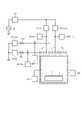
図1が示すように、プラズマ処理装置は、真空チャンバー11、ガス供給部21、排気部22、及び高周波電力回路を備える。真空チャンバー11は、ステージ12を収容する。ステージ12は、プラズマ処理の対象物Sを載置する。ガス供給部21は、プラズマを生成するための各種のガスを真空チャンバー11に供給する。排気部22は、プラズマを生成するための圧力に真空チャンバー11の内圧を調整する。 As shown in FIG. 1, the plasma processing apparatus includes a
[高周波電力回路]
高周波電力回路は、内側アンテナLin、内側分配用コンデンサVCin1、および内側共振用コンデンサVCin2を備える。内側アンテナLin、内側分配用コンデンサVCin1、および内側共振用コンデンサVCin2は、直列接続されている。[High frequency power circuit]
The high frequency power circuit includes an inner antenna Lin, an inner distribution capacitor VCin1 and an inner resonance capacitor VCin2. The inner antenna Lin, the inner distribution capacitor VCin1 and the inner resonance capacitor VCin2 are connected in series.
内側アンテナLinは、内側分配用コンデンサVCin1と内側共振用コンデンサVCin2との間に位置する。内側アンテナLinは、プラズマ生成用の環状アンテナであり、例えば、110mmの直径を有する3巻のアンテナである。内側アンテナLinは、真空チャンバー11の天面中央に配置されてもよいし、真空チャンバー11の天面他部に配置されてもよい。なお、図1には、内側アンテナLinの抵抗成分である内側抵抗Rinを説明の便宜上記載する。 The inner antenna Lin is located between the inner distribution capacitor VCin1 and the inner resonance capacitor VCin2. The inner antenna Lin is an annular antenna for plasma generation, for example, a three-roll antenna having a diameter of 110 mm. The inner antenna Lin may be arranged at the center of the top surface of the
内側分配用コンデンサVCin1は、可変コンデンサであって、内側アンテナLinにおける高周波電力の入力端に接続されている。内側共振用コンデンサVCin2は、可変コンデンサであって、内側アンテナLinにおける高周波電力の出力端に接続されている。 The inner distribution capacitor VCin1 is a variable capacitor and is connected to an input end of high frequency power in the inner antenna Lin. The inner resonance capacitor VCin2 is a variable capacitor and is connected to the output end of high frequency power in the inner antenna Lin.
内側アンテナLin、内側分配用コンデンサVCin1、および内側共振用コンデンサVCin2の各々は、第1回路要素の一例である。内側アンテナLin、内側分配用コンデンサVCin1、および内側共振用コンデンサVCin2から構成される直列回路は、第1アンテナ回路の一例である。内側アンテナLinは、第1アンテナの一例である。内側分配用コンデンサVCin1は、第1分配用コンデンサの一例である。内側共振用コンデンサVCin2は、第1可変コンデンサの一例である。 Each of the inner antenna Lin, the inner distribution capacitor VCin1, and the inner resonance capacitor VCin2 is an example of the first circuit element. The series circuit composed of the inner antenna Lin, the inner distribution capacitor VCin1 and the inner resonance capacitor VCin2 is an example of the first antenna circuit. The inner antenna Lin is an example of the first antenna. The inner distribution capacitor VCin1 is an example of a first distribution capacitor. The inner resonance capacitor VCin2 is an example of the first variable capacitor.
プラズマ処理装置は、内側電圧検知部43Vin、および内側電流検知部44Iinを備える。内側電圧検知部43Vinは、内側アンテナLinにおける電圧の一例として、内側分配用コンデンサVCin1と内側アンテナLinとの間において、内側アンテナLinの入力端電圧を検知する。内側アンテナLinにおける入力端電圧は、内側アンテナLinと内側共振用コンデンサVCin2との直列部における電圧の一例である。内側電流検知部44Iinは、内側アンテナLinに流れる電流の一例として、内側アンテナLinと内側共振用コンデンサVCin2との直列部に流れる電流を検知する。内側電圧検知部43Vinは、第1アンテナと第1可変コンデンサとの直列部における電圧を検知する第1電圧検知部の一例である。内側電流検知部44Iinは、第1アンテナと第1可変コンデンサとの直列部における電流を検知する第1電流検知部の一例である。 The plasma processing device includes an inner voltage detection unit 43Vin and an inner current detection unit 44Iin. The inner voltage detection unit 43Vin detects the input terminal voltage of the inner antenna Lin between the inner distribution capacitor VCin1 and the inner antenna Lin as an example of the voltage in the inner antenna Lin. The input end voltage in the inner antenna Lin is an example of the voltage in the series portion between the inner antenna Lin and the inner resonance capacitor VCin2. The inner current detection unit 44Iin detects the current flowing in the series portion between the inner antenna Lin and the inner resonance capacitor VCin2 as an example of the current flowing through the inner antenna Lin. The inner voltage detection unit 43Vin is an example of a first voltage detection unit that detects a voltage in a series portion between the first antenna and the first variable capacitor. The inner current detection unit 44Iin is an example of a first current detection unit that detects a current in a series portion between the first antenna and the first variable capacitor.
高周波電力回路は、外側アンテナLo、外側分配用コンデンサVCo1、および外側共振用コンデンサVCo2を備える。外側アンテナLo、外側分配用コンデンサVCo1、および外側共振用コンデンサVCo2は、直列接続されている。 The high frequency power circuit includes an outer antenna Lo, an outer distribution capacitor VCo1 and an outer resonance capacitor VCo2. The outer antenna Lo, the outer distribution capacitor VCo1 and the outer resonance capacitor VCo2 are connected in series.
外側アンテナLoは、外側分配用コンデンサVCo1と外側共振用コンデンサVCo2との間に位置する。外側アンテナLoは、プラズマ生成用の環状アンテナであり、例えば、260mmの直径を有した2巻のアンテナである。外側アンテナLoは、真空チャンバー11の天面外周に配置されて内側アンテナLinを囲ってもよいし、真空チャンバー11の天面他部において内側アンテナLinに並設されてもよい。なお、図1には、外側アンテナLoの抵抗成分である外側抵抗Roを説明の便宜上記載する。 The outer antenna Lo is located between the outer distribution capacitor VCo1 and the outer resonance capacitor VCo2. The outer antenna Lo is an annular antenna for plasma generation, for example, a two-roll antenna having a diameter of 260 mm. The outer antenna Lo may be arranged on the outer periphery of the top surface of the
外側分配用コンデンサVCo1は、可変コンデンサであって、外側アンテナLoにおける高周波電力の入力端に接続されている。外側共振用コンデンサVCo2は、可変コンデンサであって、外側アンテナLoにおける高周波電力の出力端に接続されている。 The outer distribution capacitor VCo1 is a variable capacitor and is connected to the input end of high frequency power in the outer antenna Lo. The outer resonance capacitor VCo2 is a variable capacitor and is connected to the output end of high frequency power in the outer antenna Lo.
外側アンテナLo、外側分配用コンデンサVCo1、および外側共振用コンデンサVCo2の各々は、第2回路要素の一例である。外側アンテナLo、外側分配用コンデンサVCo1、および外側共振用コンデンサVCo2から構成される直列回路は、第2アンテナ回路の一例である。外側アンテナLoは、第2アンテナの一例である。外側分配用コンデンサVCo1は、第2分配用コンデンサの一例である。外側共振用コンデンサVCo2は、第2可変コンデンサの一例である。 Each of the outer antenna Lo, the outer distribution capacitor VCo1 and the outer resonance capacitor VCo2 is an example of the second circuit element. The series circuit including the outer antenna Lo, the outer distribution capacitor VCo1 and the outer resonance capacitor VCo2 is an example of the second antenna circuit. The outer antenna Lo is an example of the second antenna. The outer distribution capacitor VCo1 is an example of a second distribution capacitor. The outer resonance capacitor VCo2 is an example of a second variable capacitor.
プラズマ処理装置は、外側電圧検知部43Vo、および外側電流検知部44Ioを備える。外側電圧検知部43Voは、外側アンテナLoにおける電圧の一例として、外側分配用コンデンサVCo1と外側アンテナLoとの間において、外側アンテナLoの入力端電圧を検知する。外側アンテナLoにおける入力端電圧は、外側アンテナLoと外側共振用コンデンサVCo2との直列部における電圧の一例である。外側電流検知部44Ioは、外側アンテナLoに流れる電流の一例として、外側アンテナLoと外側共振用コンデンサVCo2との直列部に流れる電流を検知する。外側電圧検知部43Voは、第2アンテナと第2可変コンデンサとの直列部における電圧を検知する第2電圧検知部の一例である。外側電流検知部44Ioは、第2アンテナと第2可変コンデンサとの直列部における電流を検知する第2電流検知部の一例である。 The plasma processing device includes an outer voltage detection unit 43Vo and an outer current detection unit 44Io. The outer voltage detection unit 43Vo detects the input end voltage of the outer antenna Lo between the outer distribution capacitor VCo1 and the outer antenna Lo as an example of the voltage in the outer antenna Lo. The input end voltage in the outer antenna Lo is an example of the voltage in the series portion between the outer antenna Lo and the outer resonance capacitor VCo2. The outer current detection unit 44Io detects the current flowing in the series portion between the outer antenna Lo and the outer resonance capacitor VCo2 as an example of the current flowing through the outer antenna Lo. The outer voltage detection unit 43Vo is an example of a second voltage detection unit that detects a voltage in a series portion between the second antenna and the second variable capacitor. The outer current detection unit 44Io is an example of a second current detection unit that detects a current in a series portion between the second antenna and the second variable capacitor.
内側アンテナLin、内側分配用コンデンサVCin1、および内側共振用コンデンサVCin2から構成される直列回路と、外側アンテナLo、外側分配用コンデンサVCo1、および外側共振用コンデンサVCo2から構成される直列回路とは、高周波電源41に接続された整合器42に並列接続されている。整合器42は、電力の送信側である高周波電源41のインピーダンスと、電力の受信側のインピーダンス、すなわち、整合器42や高周波電力回路を含む負荷のインピーダンスとを、特性インピーダンスに等しくする。 The series circuit composed of the inner antenna Lin, the inner distribution capacitor VCin1 and the inner resonance capacitor VCin2, and the series circuit composed of the outer antenna Lo, the outer distribution capacitor VCo1 and the outer resonance capacitor VCo2 have high frequencies. It is connected in parallel to the matching
図2が示すように、高周波電力回路の等価回路は、内側分配用コンデンサVCin1、内側アンテナLin、内側アンテナLinの抵抗成分である内側抵抗Rin、および内側共振用コンデンサVCin2から構成される直列回路を含む。高周波電力回路の等価回路は、外側分配用コンデンサVCo1、外側アンテナLo、外側アンテナLoの抵抗成分である外側抵抗Ro、および外側共振用コンデンサVCo2から構成される直列回路を含む。そして、高周波電力回路の等価回路は、これら2つの直列回路の並列回路として示される。 As shown in FIG. 2, the equivalent circuit of the high-frequency power circuit is a series circuit composed of the inner distribution capacitor VCin1, the inner antenna Lin, the inner resistance Rin which is the resistance component of the inner antenna Lin, and the inner resonance capacitor VCin2. include. The equivalent circuit of the high frequency power circuit includes a series circuit composed of the outer distribution capacitor VCo1, the outer antenna Lo, the outer resistance Ro which is a resistance component of the outer antenna Lo, and the outer resonance capacitor VCo2. The equivalent circuit of the high frequency power circuit is shown as a parallel circuit of these two series circuits.
内側電圧検知部43Vinは、内側アンテナLinの入力端電圧である内側入力端電圧Vinを検知する。外側電圧検知部43Voは、外側アンテナLoの入力端電圧である外側入力端電圧Voを検知する。内側電流検知部44Iinは、内側アンテナLinに流れる内側アンテナ電流Iinを検知する。外側電流検知部44Ioは、外側アンテナLoに流れる外側アンテナ電流Ioを検知する。 The inner voltage detection unit 43Vin detects the inner input end voltage Vin which is the input end voltage of the inner antenna Lin. The outer voltage detection unit 43Vo detects the outer input end voltage Vo, which is the input end voltage of the outer antenna Lo. The inner current detection unit 44Iin detects the inner antenna current Iin flowing through the inner antenna Lin. The outer current detection unit 44Io detects the outer antenna current Io flowing through the outer antenna Lo.
[制御部]
図3が示すように、高周波電力回路は、可変コンデンサの駆動を制御するための制御部51を備える。制御部51は、例えば、CPU、RAM、ROMなどのコンピュータに用いられるハードウェア要素、および、ソフトウェアによって構成される。制御部51は、各種の処理を全てソフトウェアで処理するものに限らない。例えば、制御部51は、各種の処理のうちの少なくとも一部の処理を実行する専用のハードウェアである特定用途向け集積回路(ASIC)を備えてもよい。制御部51は、ASICなどの1つ以上の専用のハードウェア回路、コンピュータプログラムであるソフトウェアに従って動作する1つ以上のプロセッサを含むマイクロコンピュータ、あるいは、これらの組み合わせ、を含む回路として構成してもよい。[Control unit]
As shown in FIG. 3, the high frequency power circuit includes a
制御部51は、プラズマ処理方法を実行するための各種のプログラムとデータとを記憶する。制御部51は、可変コンデンサの駆動の制御に用いる制御データ52を記憶する。制御部51は、プラズマ処理方法を実行するためのプログラムを読み出し、当該プログラムに従って処理を実行する。プラズマ処理方法は、電流分配比の目標値を設定する分配処理と、電流分配比が目標値となるように可変コンデンサを駆動する整合処理とを含む。制御部51は、プラズマが生成されていない状態で分配処理を行う。制御部51は、プラズマが生成されている状態で整合処理を行う。 The
[分配処理]
電流分配比は、外側アンテナLoの電流値と内側アンテナLinの電流値との比である。なお、電流分配比は、外側アンテナLoの電流値に対する内側アンテナLinの電流値の比でもよいし、内側アンテナLinの電流値に対する外側アンテナLoの電流値の比でもよい。[Distribution processing]
The current distribution ratio is the ratio of the current value of the outer antenna Lo to the current value of the inner antenna Lin. The current distribution ratio may be the ratio of the current value of the inner antenna Lin to the current value of the outer antenna Lo, or the ratio of the current value of the outer antenna Lo to the current value of the inner antenna Lin.
制御部51は、制御データ52を用いて分配処理を行う。制御部51は、分配処理として、内側分配用コンデンサVCin1と外側分配用コンデンサVCo1とを駆動させ、内側分配用コンデンサVCin1の容量値と外側分配用コンデンサVCo1の容量値とを、電流分配比の目標値を得るための値とする。 The
制御データ52は、電流分配比を入力として、内側分配用コンデンサVCin1の容量値と外側分配用コンデンサVCo1の容量値とを出力するためのデータである。制御データ52は、プラズマが生成されていない状態での高周波電力回路から予め理論的に算出されるデータである。制御データ52は、内側分配用コンデンサVCin1の容量値と外側分配用コンデンサVCo1の容量値とを電流分配比に対応付けたテーブルでもよい。制御データ52は、電流分配比を入力として、内側分配用コンデンサVCin1の容量値と外側分配用コンデンサVCo1の容量値とを出力する関係式でもよい。 The
制御データ52の一例は、容量分配比相関データと容量相関データとから構成される。容量分配比相関データは、電流分配比を入力として、内側分配用コンデンサVCin1の容量値と外側分配用コンデンサVCo1の容量値とのいずれか一方を出力するためのデータである。容量分配比相関データは、テーブルでもよいし関係式でもよい。容量相関データは、内側分配用コンデンサVCin1の容量値と外側分配用コンデンサVCo1の容量値とのいずれか一方を入力として他方を出力するためのデータである。容量相関データは、テーブルでもよいし関係式でもよい。 An example of the
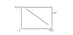
図4が示すように、容量相関データの一例は、内側分配用コンデンサVCin1の容量値と外側分配用コンデンサVCo1の容量値とを対応付けたテーブルである。容量相関データの一例では、内側分配用コンデンサVCin1の各容量値に、外側分配用コンデンサVCo1の容量値を対応付けている。容量相関データの一例において、外側分配用コンデンサVCo1の容量値が大きくなるほど内側分配用コンデンサVCin1の容量値が小さくなる。 As shown in FIG. 4, an example of the capacitance correlation data is a table in which the capacitance value of the inner distribution capacitor VCin1 and the capacitance value of the outer distribution capacitor VCo1 are associated with each other. In an example of the capacitance correlation data, the capacitance value of the outer distribution capacitor VCo1 is associated with each capacitance value of the inner distribution capacitor VCin1. In an example of capacitance correlation data, the larger the capacitance value of the outer distribution capacitor VCo1, the smaller the capacitance value of the inner distribution capacitor VCin1.
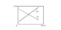
図5が示すように、容量分配比相関データの一例は、内側分配用コンデンサVCin1の容量値と電流分配比とを対応付けたテーブルである。容量分配比相関データの一例では、内側分配用コンデンサVCin1の各容量値に、内側アンテナLinの電流値Irms(図5において内側アンテナ電流Iinの値)と外側アンテナLoの電流値Irms(図5において外側アンテナ電流Ioの値)とを対応付けている。容量分配比相関データの一例において、内側分配用コンデンサVCin1の容量値が大きくなるほど、内側アンテナLinの電流値Irmsが大きく、かつ外側アンテナLoの電流値Irmsが小さくなる。なお、容量分配比相関データの一例は、外側分配用コンデンサVCo1の容量値に、内側アンテナLinの電流値Irmsと外側アンテナLoの電流値Irmsとを対応付けてもよい。 As shown in FIG. 5, an example of the capacitance distribution ratio correlation data is a table in which the capacitance value of the inner distribution capacitor VCin1 and the current distribution ratio are associated with each other. In an example of the capacitance distribution ratio correlation data, the current value Irms of the inner antenna Lin (the value of the inner antenna current Iin in FIG. 5) and the current value Irms of the outer antenna Lo (in FIG. 5) are added to each capacitance value of the inner distribution capacitor VCin1. It is associated with the value of the outer antenna current Io). In an example of the capacitance distribution ratio correlation data, the larger the capacitance value of the inner distribution capacitor VCin1, the larger the current value Irms of the inner antenna Lin and the smaller the current value Irms of the outer antenna Lo. As an example of the capacitance distribution ratio correlation data, the capacitance value of the outer distribution capacitor VCo1 may be associated with the current value Irms of the inner antenna Lin and the current value Irms of the outer antenna Lo.
制御部51は、容量分配比相関データを用い、電流分配比から、内側分配用コンデンサVCin1と外側分配用コンデンサVCo1とのいずれか一方の容量値を導く。制御部51は、容量相関データを用い、内側分配用コンデンサVCin1と外側分配用コンデンサVCo1とのいずれか一方の容量値から、他方の容量値を導く。これにより、制御部51は、内側分配用コンデンサVCin1と外側分配用コンデンサVCo1とのいずれか一方の駆動に他方の駆動を連動させる。 The
[整合処理]
図3に戻り、制御部51は、内側電圧検知部43Vinの検知結果と、内側電流検知部44Iinの検知結果とを入力として、整合処理を行う。制御部51は、整合処理として、内側アンテナLinと内側共振用コンデンサVCin2との直列部の電流と電圧との位相差を算出し、当該位相差が小さくなるように内側共振用コンデンサVCin2の容量値を設定する。制御部51は、プラズマが生成される期間の全体にわたり、整合処理を繰り返して行う。制御部51は、内側電圧検知部43Vinの検知結果と、内側電流検知部44Iinの検知結果とが入力される周期で整合処理を行ってもよいし、当該周期とは異なる所定の制御周期で整合処理を行ってもよい。[Alignment processing]
Returning to FIG. 3, the
制御部51は、整合処理の一例として、内側電圧検知部43Vinの検知結果から、内側アンテナLinに供給される電圧の位相を得る。また、制御部51は、整合処理の一例として、内側電流検知部44Iinの検知結果から、内側アンテナLinに流れる電流の位相を得る。そして、制御部51は、整合処理の一例として、内側アンテナLinと内側共振用コンデンサVCin2との直列部に供給される電圧の位相と、内側アンテナLinと内側共振用コンデンサVCin2との直列部に流れる電流の位相とを一致させる内側共振用コンデンサVCin2の容量値をこれらの位相差から算出する。制御部51は、内側共振用コンデンサVCin2の容量値が算出値になるように、内側共振用コンデンサVCin2を駆動する。 As an example of the matching process, the
プラズマが生成されている状態では、プラズマ生成によるインピーダンス成分がアンテナ回路のインピーダンスに回路定数として現れるから、プラズマが生成されていない状態で理論的に求められた共振条件と実際の共振条件との間に乖離が生じる。制御部51は、内側アンテナLinに供給される電圧の位相と内側アンテナLinに流れる電流の位相とを一致させる、言い換えれば、理論的に求められた共振条件と実際の共振条件との間の乖離を抑えるように、内側共振用コンデンサVCin2の容量値を動的に設定し続ける。 In the state where plasma is generated, the impedance component due to plasma generation appears as a circuit constant in the impedance of the antenna circuit. Therefore, between the resonance condition theoretically obtained in the state where plasma is not generated and the actual resonance condition. There is a divergence in. The
制御部51は、外側電圧検知部43Voの検知結果と、外側電流検知部44Ioの検知結果とを入力として、さらに整合処理を行う。制御部51は、整合処理として、外側アンテナLoと外側共振用コンデンサVCo2との直列部の電流と電圧との位相差を算出し、当該位相差が小さくなるように外側共振用コンデンサVCo2の容量値を設定する。 The
制御部51は、整合処理の一例として、外側電圧検知部43Voの検知結果から、外側アンテナLoに供給される電圧の位相を得る。また、制御部51は、整合処理の一例として、外側電流検知部44Ioの検知結果から、外側アンテナLoに流れる電流の位相を得る。そして、制御部51は、整合処理の一例として、外側アンテナLoと外側共振用コンデンサVCo2との直列部に供給される電圧の位相と、外側アンテナLoと外側共振用コンデンサVCo2との直列部に流れる電流の位相とを一致させる外側共振用コンデンサVCo2の容量値をこれらの位相差から算出する。制御部51は、外側共振用コンデンサVCo2の容量値が算出値になるように、外側共振用コンデンサVCo2を駆動する。 As an example of the matching process, the
制御部51は、外側アンテナLoに供給される電圧の位相と外側アンテナLoに流れる電流の位相とを一致させる。言い換えれば、制御部51は、理論的に求められた共振条件と実際の共振条件との間の乖離を抑えるように、内側共振用コンデンサVCin2の容量値の設定と同じタイミングで、外側共振用コンデンサVCo2の容量値を動的に設定する。 The
図6は、分配処理によって設定された内側分配用コンデンサVCin1の容量値と、整合処理によって設定された内側共振用コンデンサVCin2における容量値の実測値との関係の一例を示す。また、図6は、分配処理によって設定された内側分配用コンデンサVCin1の容量値と、整合処理によって設定された外側共振用コンデンサVCo2における容量値の実測値との関係の一例を示す。なお、上述したように、外側分配用コンデンサVCo1の容量値は、内側分配用コンデンサVCin1の容量値を設定するための分配処理において、内側分配用コンデンサVCin1の容量値が設定される都度、制御データ52に基づいて一義的に設定される。 FIG. 6 shows an example of the relationship between the capacitance value of the inner distribution capacitor VCin1 set by the distribution process and the measured value of the capacitance value of the inner resonance capacitor VCin2 set by the matching process. Further, FIG. 6 shows an example of the relationship between the capacitance value of the inner distribution capacitor VCin1 set by the distribution process and the measured value of the capacitance value of the outer resonance capacitor VCo2 set by the matching process. As described above, the capacitance value of the outer distribution capacitor VCo1 is the control data each time the capacitance value of the inner distribution capacitor VCin1 is set in the distribution process for setting the capacitance value of the inner distribution capacitor VCin1. It is uniquely set based on 52.
図6が示すように、内側分配用コンデンサVCin1の容量値が大きくなるほど、すなわち内側アンテナLinの電流値が大きくなるほど、内側共振用コンデンサVCin2の容量値は、徐々に大きくなる。なお、内側共振用コンデンサVCin2の容量値が変わる度合いと、内側分配用コンデンサVCin1の容量値が変わる度合いとの関係は、一定であるとはいえず、電流分配比などの生成条件の変更内容、ひいては、プラズマ生成により生じるインピーダンス成分が変わる度合いによって変わり得る。 As shown in FIG. 6, as the capacitance value of the inner distribution capacitor VCin1 increases, that is, as the current value of the inner antenna Lin increases, the capacitance value of the inner resonance capacitor VCin2 gradually increases. The relationship between the degree to which the capacitance value of the inner resonance capacitor VCin2 changes and the degree to which the capacitance value of the inner distribution capacitor VCin1 changes is not constant, and the content of changes in the generation conditions such as the current distribution ratio, As a result, it may change depending on the degree to which the impedance component generated by plasma generation changes.
また、内側分配用コンデンサVCin1の容量値が大きくなるほど、外側共振用コンデンサVCo2の容量値は、徐々に小さくなる。ここでも、外側共振用コンデンサVCo2の容量値が変わる度合いと、内側分配用コンデンサVCin1の容量値が変わる度合いとの関係は、一定であるとはいえず、電流分配比などの生成条件の変更内容、ひいては、プラズマ生成により生じるインピーダンス成分が変わる度合いによって変わり得る。 Further, as the capacitance value of the inner distribution capacitor VCin1 increases, the capacitance value of the outer resonance capacitor VCo2 gradually decreases. Again, the relationship between the degree to which the capacitance value of the outer resonance capacitor VCo2 changes and the degree to which the capacitance value of the inner distribution capacitor VCin1 changes is not constant, and the content of changes in the generation conditions such as the current distribution ratio. As a result, the impedance component generated by plasma generation may change depending on the degree of change.
このように、内側分配用コンデンサVCin1の容量値が変わることは、プラズマ生成によるインピーダンス成分の発生などにより見かけ上の内側アンテナLinのインピーダンスが変わることである。また、プラズマ生成により生じるインピーダンス成分は、プラズマ処理における対象物Sの状況や真空チャンバー11の状態などによっても変わり得るものである。この点、プラズマ生成により生じるインピーダンス成分が変わることによって生じ得る内側アンテナLinと内側共振用コンデンサVCin2との直列部の電流と電圧との位相差は、内側共振用コンデンサVCin2の容量値が動的に変わることによって抑えられる。同時に、プラズマ生成により生じるインピーダンス成分が変わることによって生じ得る外側アンテナLoと外側共振用コンデンサVCo2との直列部の電流と電圧との位相差は、外側共振用コンデンサVCo2の容量値が動的に変わることによって抑えられる。 In this way, the change in the capacitance value of the inner distribution capacitor VCin1 means that the apparent impedance of the inner antenna Lin changes due to the generation of an impedance component due to plasma generation or the like. Further, the impedance component generated by plasma generation can change depending on the state of the object S in the plasma processing, the state of the
これにより、内側アンテナLinと内側共振用コンデンサVCin2との直列部がほぼ共振している状態となり得ると共に、外側アンテナLoと外側共振用コンデンサVCo2との直列部もまたほぼ共振している状態となり得る。結果として、内側アンテナLinを含む直列回路のインピーダンスと、外側アンテナLoを含む直列回路のインピーダンスとの比と、プラズマが生成されていない状態において理論的に求められた比との間に乖離が生じることが抑えられる。 As a result, the series portion between the inner antenna Lin and the inner resonance capacitor VCin2 may be in a state of being substantially resonating, and the series portion of the outer antenna Lo and the outer resonance capacitor VCo2 may also be in a state of being substantially resonating. .. As a result, there is a discrepancy between the impedance of the series circuit including the inner antenna Lin and the impedance of the series circuit including the outer antenna Lo and the ratio theoretically obtained in the state where the plasma is not generated. Is suppressed.
[プラズマ処理方法]
上記プラズマ処理装置の作用として当該プラズマ処理装置が実行するプラズマ処理方法について説明する。プラズマ処理方法は、上述したように、電流分配比の目標値を設定する分配処理と、電流分配比が目標値となるように可変コンデンサを駆動する整合処理とを含む。[Plasma processing method]
The plasma processing method executed by the plasma processing apparatus as the operation of the plasma processing apparatus will be described. As described above, the plasma processing method includes a distribution process for setting a target value of the current distribution ratio and a matching process for driving a variable capacitor so that the current distribution ratio becomes the target value.
まず、プラズマ処理装置は、真空チャンバー11に対象物Sを収容する。次いで、プラズマ処理装置は、プラズマを生成するためのガスをガス供給部21から真空チャンバー11に供給する。また、プラズマ処理装置は、プラズマを生成するための圧力に真空チャンバー11の内圧を調整する。 First, the plasma processing apparatus accommodates the object S in the
この間、制御部51は、プラズマを生成するための条件のうちの電流分配比を参照し、制御データ52を用いて分配処理を行う。すなわち、内側分配用コンデンサVCin1と外側分配用コンデンサVCo1とを駆動させ、内側分配用コンデンサVCin1の容量値と外側分配用コンデンサVCo1の容量値とを、電流分配比の目標値を得るための値とする。 During this time, the
次いで、プラズマ処理装置は、高周波電源41から高周波電力を供給し、真空チャンバー11の内部にプラズマを生成する。この間、制御部51は、内側電圧検知部43Vinの検知結果と、内側電流検知部44Iinの検知結果とを入力として、整合処理を行う。すなわち、制御部51は、内側アンテナLinと内側共振用コンデンサVCin2との直列部の電流と電圧との位相差を算出し、当該位相差が小さくなるように内側共振用コンデンサVCin2の容量値を動的に設定し続ける。同時に、制御部51は、外側アンテナLoと外側共振用コンデンサVCo2との直列部の電流と電圧との位相差を算出し、当該位相差が小さくなるように外側共振用コンデンサVCo2の容量値を動的に設定し続ける。 Next, the plasma processing device supplies high-frequency power from the high-
以上、上記実施形態によれば、以下の効果を得ることができる。 As described above, according to the above embodiment, the following effects can be obtained.
(1)プラズマ生成時における内側アンテナLinと内側共振用コンデンサVCin2との直列部の電流と電圧との位相差が小さくなるように、内側共振用コンデンサVCin2の容量値が設定される。また、プラズマ生成時における外側アンテナLoと外側共振用コンデンサVCo2との直列部の電流と電圧との位相差が小さくなるように、外側共振用コンデンサVCo2の容量値が設定される。これにより、プラズマが生成されている状態であっても、内側アンテナLinを含む直列回路のインピーダンスと、外側アンテナLoを含む直列回路のインピーダンスとの比は、プラズマが生成されていない状態において理論的に求められた比に相当するものとなる。結果として、プラズマが生成されていない状態において理論的に求められた電流分配比と実際の電流分配比との間に乖離が生じることが抑えられる。 (1) The capacitance value of the inner resonance capacitor VCin2 is set so that the phase difference between the current and the voltage in the series portion between the inner antenna Lin and the inner resonance capacitor VCin2 at the time of plasma generation becomes small. Further, the capacitance value of the outer resonance capacitor VCo2 is set so that the phase difference between the current and the voltage in the series portion between the outer antenna Lo and the outer resonance capacitor VCo2 at the time of plasma generation becomes small. As a result, even when plasma is generated, the ratio of the impedance of the series circuit including the inner antenna Lin and the impedance of the series circuit including the outer antenna Lo is theoretical in the state where plasma is not generated. It corresponds to the ratio required for. As a result, it is possible to prevent a discrepancy between the theoretically obtained current distribution ratio and the actual current distribution ratio in the state where plasma is not generated.
(2)LC並列回路のように大きな電流が流れるアンテナ回路では、アンテナ回路を構成する各回路要素の特性に、熱的な不安定性が潜在する。この点、上述した高周波電力回路は、LC並列回路を含まない直列回路で構成されるから、アンテナや可変コンデンサなどの回路要素に潜在する熱的な不安定性を抑えることが可能ともなる。 (2) In an antenna circuit such as an LC parallel circuit in which a large current flows, thermal instability is latent in the characteristics of each circuit element constituting the antenna circuit. In this respect, since the high-frequency power circuit described above is composed of a series circuit that does not include the LC parallel circuit, it is possible to suppress the thermal instability latent in the circuit elements such as the antenna and the variable capacitor.
(3)プラズマ生成時における内側アンテナLinと内側共振用コンデンサVCin2との直列部の電流と電圧との位相が一致するように、内側共振用コンデンサVCin2の容量値が設定される。また、プラズマ生成時における外側アンテナLoと外側共振用コンデンサVCo2との直列部の電流と電圧との位相が一致するように、外側共振用コンデンサVCo2の容量値が設定される。これにより、上記(1)に準じた効果の実効性が高められる。 (3) The capacitance value of the inner resonance capacitor VCin2 is set so that the phases of the current and the voltage in the series portion between the inner antenna Lin and the inner resonance capacitor VCin2 at the time of plasma generation match. Further, the capacitance value of the outer resonance capacitor VCo2 is set so that the phases of the current and the voltage in the series portion between the outer antenna Lo and the outer resonance capacitor VCo2 at the time of plasma generation match. As a result, the effectiveness of the effect according to the above (1) is enhanced.
(4)制御データ52を用い、内側分配用コンデンサVCin1の駆動と外側分配用コンデンサVCo1の駆動との連動を通じて、高周波電源41が電力を供給する前に、内側分配用コンデンサVCin1の容量値と外側分配用コンデンサVCo1の容量値とが設定される。これにより、互いに異なる複数の電流分配比においても、上記(1)に準じた効果が得られる。 (4) Using the
なお、上記実施形態は、以下のように変更して実施できる。また、上記実施形態と以下の各変更例、および変更例同士は、技術的に矛盾しない範囲で互いに組み合わせて実施することができる。 The above embodiment can be modified and implemented as follows. Further, the above embodiment, each of the following modified examples, and the modified examples can be implemented in combination with each other within a technically consistent range.
・図7が示すように、内側共振用コンデンサVCin2は、内側分配用コンデンサVCin1と内側アンテナLinとの間に位置してもよい。また、外側共振用コンデンサVCo2は、外側分配用コンデンサVCo1と外側アンテナLoとの間に位置してもよい。こうした構成であっても、上記(1)から(4)に準じた効果を得ることは可能である。 As shown in FIG. 7, the inner resonance capacitor VCin2 may be located between the inner distribution capacitor VCin1 and the inner antenna Lin. Further, the outer resonance capacitor VCo2 may be located between the outer distribution capacitor VCo1 and the outer antenna Lo. Even with such a configuration, it is possible to obtain the effects according to the above (1) to (4).
・図8が示すように、内側電圧検知部43Vinは、内側アンテナLinが備える2つの端において、内側入力端電圧Vinにおけるピーク間電圧Vppと、出力端電圧である内側出力端電圧Vin2におけるピーク間電圧Vppとを別々に検知してもよい。また、内側アンテナLinの長さは、内側アンテナLinにおける上記各ピーク間電圧Vppが内側アンテナLinの長さに対して線形に変わるように設定されてもよい。 As shown in FIG. 8, in the inner voltage detection unit 43Vin, at the two ends of the inner antenna Lin, between the peak voltage Vpp at the inner input end voltage Vin and the peak at the inner output end voltage Vin2 which is the output end voltage. The voltage Vpp may be detected separately. Further, the length of the inner antenna Lin may be set so that the voltage Vpp between the peaks in the inner antenna Lin changes linearly with respect to the length of the inner antenna Lin.
内側アンテナLinにおけるピーク間電圧Vppが内側アンテナLinの長さに対して線形に変化する構成であれば、内側入力端電圧Vinにおけるピーク間電圧Vppと、内側出力端電圧Vin2におけるピーク間電圧Vppとを用い、内側アンテナLinにおける電圧分布、すなわち共振点を推定することが可能となる。 If the inter-peak voltage Vpp in the inner antenna Lin changes linearly with respect to the length of the inner antenna Lin, the inter-peak voltage Vpp in the inner input end voltage Vin and the inter-peak voltage Vpp in the inner output end voltage Vin2 It is possible to estimate the voltage distribution in the inner antenna Lin, that is, the resonance point.
制御部51は、整合処理において、内側電圧検知部43Vinの検知結果から内側アンテナLinにおける共振点を推定し、推定結果を外部に出力してもよい。これによれば、プラズマが生成されている状態で、内側アンテナLinにおける共振点がどこに存在するか、ひいては内側アンテナLinによって生成されるプラズマの分布を推定することが可能となる。 In the matching process, the
さらに、制御部51は、整合処理において、内側アンテナLinでの位相差が小さくなるように設定された内側共振用コンデンサVCin2の容量値と、内側分配用コンデンサVCin1の容量値との合成容量を保つように構成されてもよい。加えて、制御部51は、共振点が目標位置となるように、合成容量を保ちながら、内側分配用コンデンサVCin1の容量値と、内側共振用コンデンサVCin2の容量値とを再設定してもよい。 Further, in the matching process, the
この際、制御部51は、現在の共振点と目標位置との差を入力として、目標位置を得るための、内側分配用コンデンサVCin1の容量値と内側共振用コンデンサVCin2の容量値との比を出力する新たな制御データを予め記憶する。そして、制御部51は、共振点の推定結果と目標位置とを制御データに適用し、合成容量を保ちながら、内側分配用コンデンサVCin1の容量値と、内側共振用コンデンサVCin2の容量値とを再設定してもよい。 At this time, the
これにより、プラズマが生成されていない状態において理論的に求められた電流分配比と実際の電流分配比との間に乖離が生じることを抑えながらも、内側アンテナLinにおける電圧分布、ひいては、内側アンテナLinよって生成されるプラズマの分布を変えることが可能ともなる。 As a result, the voltage distribution in the inner antenna Lin, and eventually the inner antenna, while suppressing the divergence between the theoretically obtained current distribution ratio and the actual current distribution ratio in the state where plasma is not generated. It is also possible to change the distribution of plasma generated by Lin.
・また、図8が示すように、外側電圧検知部43Voは、外側アンテナLoが備える2つの端において、外側入力端電圧Voにおけるピーク間電圧Vppと、出力端電圧である外側出力端電圧Vo2におけるピーク間電圧Vppとを別々に検知してもよい。また、外側アンテナLoの長さは、外側アンテナLoにおける上記各ピーク間電圧Vppが外側アンテナLoの長さに対して線形に変わるように設定されてもよい。 Further, as shown in FIG. 8, the outer
外側アンテナLoにおけるピーク間電圧Vppが外側アンテナLoの長さに対して線形に変化する構成であれば、外側入力端電圧Voにおけるピーク間電圧Vppと、外側出力端電圧Vo2におけるピーク間電圧Vppとを用い、外側アンテナLoにおける電圧分布、すなわち共振点を推定することが可能となる。 If the inter-peak voltage Vpp in the outer antenna Lo changes linearly with respect to the length of the outer antenna Lo, the inter-peak voltage Vpp at the outer input end voltage Vo and the inter-peak voltage Vpp at the outer output end voltage Vo2 Can be used to estimate the voltage distribution at the outer antenna Lo, that is, the resonance point.
制御部51は、整合処理において、外側電圧検知部43Voの検知結果から外側アンテナLoにおける共振点を推定し、推定結果を外部に出力してもよい。これによれば、プラズマが生成されている状態で、外側アンテナLoにおける共振点がどこに存在するか、ひいては外側アンテナLoによって生成されるプラズマの分布を推定することが可能となる。 In the matching process, the
さらに、制御部51は、整合処理において、外側アンテナLoでの位相差が小さくなるように設定された外側共振用コンデンサVCo2の容量値と、外側分配用コンデンサVCo1の容量値との合成容量を保つように構成されてもよい。加えて、制御部51は、共振点が目標位置となるように、合成容量を保ちながら、外側分配用コンデンサVCo1の容量値と、外側共振用コンデンサVCo2の容量値とを再設定してもよい。 Further, the
この際、制御部51は、現在の共振点と目標位置との差を入力として、目標位置を得るための、外側分配用コンデンサVCo1の容量値と外側共振用コンデンサVCo2の容量値との比を出力する新たな制御データを予め記憶する。そして、制御部51は、共振点の推定結果と目標位置とを制御データに適用し、合成容量を保ちながら、外側分配用コンデンサVCo1の容量値と、外側共振用コンデンサVCo2の容量値とを再設定してもよい。 At this time, the
これにより、プラズマが生成されていない状態において理論的に求められた電流分配比と実際の電流分配比との間に乖離が生じることを抑えながらも、外側アンテナLoにおける電圧分布、ひいては、外側アンテナLoよって生成されるプラズマの分布を変えることが可能ともなる。 As a result, the voltage distribution in the outer antenna Lo, and eventually the outer antenna, while suppressing the divergence between the theoretically obtained current distribution ratio and the actual current distribution ratio in the state where plasma is not generated. It is also possible to change the distribution of the plasma generated by Lo.
・内側アンテナLinは、環状アンテナに限らず、各種の形状に変更することが可能であり、一例として線状アンテナに変更することが可能でもある。外側アンテナLoもまた、環状アンテナに限らず、各種の形状に変更することが可能であり、一例として線状アンテナに変更することが可能でもある。 -The inner antenna Lin can be changed to various shapes, not limited to the annular antenna, and can be changed to a linear antenna as an example. The outer antenna Lo is not limited to the annular antenna, but can be changed to various shapes, and can be changed to a linear antenna as an example.
Lin…内側アンテナ
Lo…外側アンテナ
S…対象物
VCin1…内側分配用コンデンサ
VCo1…外側分配用コンデンサ
VCin2…内側共振用コンデンサ
VCo2…外側共振用コンデンサ
Rin…内側抵抗
Ro…外側抵抗
11…真空チャンバー
12…ステージ
21…ガス供給部
22…排気部
41…高周波電源
42…整合器
43Vin…内側電圧検知部
43Vo…外側電圧検知部
44Iin…内側電流検知部
44Io…外側電流検知部
51…制御部Lin ... Inner antenna Lo ... Outer antenna S ... Object VCin1 ... Inner distribution capacitor VCo1 ... Outer distribution capacitor VCin2 ... Inner resonance capacitor VCo2 ... Outer resonance capacitor Rin ... Inner resistance Ro ...
Claims (9)
Translated fromJapanese複数の第2回路要素が直列接続された第2アンテナ回路と、を備え、
高周波電源に接続された整合器に前記第1アンテナ回路と前記第2アンテナ回路とが並列接続され、
前記第1回路要素の駆動と前記第2回路要素の駆動とを制御する制御部をさらに備える高周波電力回路であって、
前記複数の第1回路要素は、プラズマ生成用の第1アンテナと、前記第1アンテナと前記整合器との間に位置する第1分配用コンデンサと、第1可変コンデンサとを備え、
前記複数の第2回路要素は、プラズマ生成用の第2アンテナと、前記第2アンテナと前記整合器との間に位置する第2分配用コンデンサと、第2可変コンデンサとを備え、
前記制御部は、
プラズマ生成時における前記第1アンテナと前記第1可変コンデンサとの直列部の電流と電圧との位相差の検知結果に基づいて当該位相差が小さくなるように前記第1可変コンデンサの容量値を設定し、かつ、
プラズマ生成時における前記第2アンテナと前記第2可変コンデンサとの直列部の電流と電圧との位相差の検知結果に基づいて当該位相差が小さくなるように前記第2可変コンデンサの容量値を設定する
高周波電力回路。A first antenna circuit in which a plurality of first circuit elements are connected in series,
A second antenna circuit in which a plurality of second circuit elements are connected in series is provided.
The first antenna circuit and the second antenna circuit are connected in parallel to a matching unit connected to a high frequency power supply.
A high-frequency power circuit further comprising a control unit for controlling the drive of the first circuit element and the drive of the second circuit element.
The plurality of first circuit elements include a first antenna for plasma generation, a first distribution capacitor located between the first antenna and the matching capacitor, and a first variable capacitor.
The plurality of second circuit elements include a second antenna for plasma generation, a second distribution capacitor located between the second antenna and the matching capacitor, and a second variable capacitor.
The control unit
The capacitance value of the first variable capacitor is set so that the phase difference becomes small based on the detection result of the phase difference between the current and the voltage in the series portion between the first antenna and the first variable capacitor at the time of plasma generation. And then
The capacitance value of the second variable capacitor is set so that the phase difference becomes small based on the detection result of the phase difference between the current and the voltage in the series portion between the second antenna and the second variable capacitor at the time of plasma generation. High frequency power circuit.
前記第2アンテナは、前記第2分配用コンデンサと前記第2可変コンデンサとの間に位置する
請求項1に記載の高周波電力回路。The first antenna is located between the first distribution capacitor and the first variable capacitor.
The high-frequency power circuit according to claim 1, wherein the second antenna is located between the second distribution capacitor and the second variable capacitor.
前記第2可変コンデンサは、前記第2分配用コンデンサと前記第2アンテナとの間に位置する
請求項1に記載の高周波電力回路。The first variable capacitor is located between the first distribution capacitor and the first antenna.
The high-frequency power circuit according to claim 1, wherein the second variable capacitor is located between the second distribution capacitor and the second antenna.
前記第1アンテナにおける電圧を検知する第1電圧検知部と、
前記第2アンテナにおける電流を検知する第2電流検知部と、
前記第2アンテナにおける電圧を検知する第2電圧検知部と、を備え、
前記制御部は、
前記第1電流検知部と前記第1電圧検知部との検知結果に基づいて前記第1アンテナと前記第1可変コンデンサとの直列部における電流の位相と電圧の位相とが一致するように前記第1可変コンデンサの容量値を設定し、かつ、
前記第2電流検知部と前記第2電圧検知部との検知結果に基づいて前記第2アンテナと前記第2可変コンデンサとの直列部における電流の位相と電圧の位相とが一致するように前記第2可変コンデンサの容量値を設定する
請求項1から3のいずれか一項に記載の高周波電力回路。The first current detection unit that detects the current in the first antenna,
The first voltage detection unit that detects the voltage in the first antenna,
A second current detection unit that detects the current in the second antenna,
A second voltage detecting unit for detecting the voltage in the second antenna is provided.
The control unit
Based on the detection result of the first current detection unit and the first voltage detection unit, the first is such that the phase of the current and the phase of the voltage in the series portion of the first antenna and the first variable capacitor match. Set the capacitance value of 1 variable capacitor, and
Based on the detection result of the second current detection unit and the second voltage detection unit, the first phase of the current and the phase of the voltage in the series portion of the second antenna and the second variable capacitor match. 2. The high-frequency power circuit according to any one of claims 1 to 3, which sets a capacitance value of a variable capacitor.
前記制御部は、
前記高周波電源が電力を供給する前に、前記第1アンテナの電流値と前記第2アンテナの電流値との比の目標値を設定する処理を行い、当該処理は、前記第1分配用コンデンサの容量値が大きくなるほど前記第2分配用コンデンサの容量値が小さくなるように前記第1分配用コンデンサの駆動に前記第2分配用コンデンサの駆動を連動させて前記第1分配用コンデンサおよび前記第2分配用コンデンサの各容量値を設定することである
請求項4に記載の高周波電力回路。The first distribution capacitor and the second distribution capacitor are variable capacitors, and are
The control unit
Before the high-frequency power supply supplies power, a process of setting a target value of the ratio between the current value of the first antenna and the current value of the second antenna is performed, and the process is performed on the first distribution capacitor. The drive of the first distribution capacitor is interlocked with the drive of the first distribution capacitor so that the capacity value of the second distribution capacitor becomes smaller as the capacitance value becomes larger, and the first distribution capacitor and the second distribution capacitor are linked. The high frequency power circuit according to claim 4, wherein each capacitance value of the distribution capacitor is set.
前記制御部は、
前記第1アンテナと前記第1可変コンデンサとの直列部の電流と電圧との位相差の検知結果に基づいて当該位相差が小さくなるように設定された前記第1可変コンデンサの容量値と、前記第1分配用コンデンサの容量値との合成容量を保ち、かつ、前記第1電圧検知部の検知結果に基づいて得られた前記第1アンテナにおける電圧分布を変えるように、前記第1可変コンデンサの容量値と、前記第1分配用コンデンサの容量値とを再設定する
請求項5に記載の高周波電力回路。The first voltage detection unit separately detects the voltages at the two ends of the first antenna.
The control unit
The capacitance value of the first variable capacitor set so that the phase difference becomes small based on the detection result of the phase difference between the current and the voltage in the series portion between the first antenna and the first variable capacitor, and the said. The first variable capacitor keeps the combined capacity with the capacity value of the first distribution capacitor and changes the voltage distribution in the first antenna obtained based on the detection result of the first voltage detection unit. The high frequency power circuit according to claim 5, wherein the capacitance value and the capacitance value of the first distribution capacitor are reset.
前記制御部は、
前記第2アンテナと前記第2可変コンデンサとの直列部の電流と電圧との位相差の検知結果に基づいて当該位相差が小さくなるように設定された前記第2可変コンデンサの容量値と、前記第2分配用コンデンサの容量値との合成容量を保ち、かつ、前記第2電圧検知部の検知結果に基づいて得られた前記第2アンテナにおける電圧分布を変えるように、前記第2可変コンデンサの容量値と、前記第2分配用コンデンサの容量値とを再設定する
請求項6に記載の高周波電力回路。The second voltage detection unit separately detects the voltages at the two ends of the second antenna.
The control unit
The capacitance value of the second variable capacitor set so that the phase difference becomes small based on the detection result of the phase difference between the current and the voltage in the series portion between the second antenna and the second variable capacitor, and the said. The second variable capacitor keeps the combined capacity with the capacity value of the second distribution capacitor and changes the voltage distribution in the second antenna obtained based on the detection result of the second voltage detection unit. The high frequency power circuit according to claim 6, wherein the capacitance value and the capacitance value of the second distribution capacitor are reset.
前記真空チャンバーの外部に設けられたプラズマを生成するための高周波電力回路と、を備え、
前記高周波電力回路は、請求項1から7のいずれか一項に記載の高周波電力回路である
プラズマ処理装置。With a vacuum chamber,
A high-frequency power circuit for generating plasma provided outside the vacuum chamber is provided.
The high-frequency power circuit is the plasma processing apparatus according to any one of claims 1 to 7.
高周波電力回路から前記真空チャンバーに高周波電力を供給すること、
を含むプラズマ処理方法であって、
前記高周波電力回路は、
複数の第1回路要素が直列接続された第1アンテナ回路と、
複数の第2回路要素が直列接続された第2アンテナ回路と、を備え、
高周波電源に接続された整合器に前記第1アンテナ回路と前記第2アンテナ回路とが並列接続され、
前記複数の第1回路要素は、プラズマ生成用の第1アンテナと、前記第1アンテナと前記整合器との間に位置する第1分配用コンデンサと、第1可変コンデンサとを備え、
前記複数の第2回路要素は、プラズマ生成用の第2アンテナと、前記第2アンテナと前記整合器との間に位置する第2分配用コンデンサと、第2可変コンデンサとを備え、
前記高周波電力を供給することは、
前記第1アンテナと前記第1可変コンデンサとの直列部の電流と電圧との位相差の検知結果に基づいて当該位相差が小さくなるように前記第1可変コンデンサの容量値を設定すること、および、
前記第2アンテナと前記第2可変コンデンサとの直列部の電流と電圧との位相差の検知結果に基づいて当該位相差が小さくなるように前記第2可変コンデンサの容量値を設定すること、を含む
プラズマ処理方法。Supplying gas into the vacuum chamber and
Supplying high-frequency power from the high-frequency power circuit to the vacuum chamber,
It is a plasma processing method including
The high frequency power circuit is
A first antenna circuit in which a plurality of first circuit elements are connected in series,
A second antenna circuit in which a plurality of second circuit elements are connected in series is provided.
The first antenna circuit and the second antenna circuit are connected in parallel to a matching unit connected to a high frequency power supply.
The plurality of first circuit elements include a first antenna for plasma generation, a first distribution capacitor located between the first antenna and the matching capacitor, and a first variable capacitor.
The plurality of second circuit elements include a second antenna for plasma generation, a second distribution capacitor located between the second antenna and the matching capacitor, and a second variable capacitor.
Supplying the high frequency power is
The capacitance value of the first variable capacitor is set so that the phase difference becomes small based on the detection result of the phase difference between the current and the voltage in the series portion between the first antenna and the first variable capacitor. ,
The capacitance value of the second variable capacitor is set so that the phase difference becomes small based on the detection result of the phase difference between the current and the voltage in the series portion between the second antenna and the second variable capacitor. Plasma processing method including.
Applications Claiming Priority (3)
| Application Number | Priority Date | Filing Date | Title |
|---|---|---|---|
| JP2020193677 | 2020-11-20 | ||
| JP2020193677 | 2020-11-20 | ||
| PCT/JP2021/030948WO2022107407A1 (en) | 2020-11-20 | 2021-08-24 | High-frequency power circuit, plasma processing device, and plasma processing method |
Publications (2)
| Publication Number | Publication Date |
|---|---|
| JP7052162B1true JP7052162B1 (en) | 2022-04-11 |
| JPWO2022107407A1 JPWO2022107407A1 (en) | 2022-05-27 |
Family
ID=80976360
Family Applications (1)
| Application Number | Title | Priority Date | Filing Date |
|---|---|---|---|
| JP2022502496AActiveJP7052162B1 (en) | 2020-11-20 | 2021-08-24 | High frequency power circuits, plasma processing equipment, and plasma processing methods |
Country Status (4)
| Country | Link |
|---|---|
| US (1) | US11665809B2 (en) |
| JP (1) | JP7052162B1 (en) |
| KR (1) | KR102475206B1 (en) |
| CN (1) | CN114303227B (en) |
Families Citing this family (3)
| Publication number | Priority date | Publication date | Assignee | Title |
|---|---|---|---|---|
| KR102475206B1 (en)* | 2020-11-20 | 2022-12-07 | 가부시키가이샤 알박 | High frequency power circuit, plasma processing device and plasma processing method |
| US20240347317A1 (en)* | 2023-04-11 | 2024-10-17 | Tokyo Electron Limited | Method and System for Plasma Processing |
| KR102855356B1 (en)* | 2024-07-18 | 2025-09-04 | (주)아센디아 | Power supply device, power supply method and plasma processing apparatus |
Citations (9)
| Publication number | Priority date | Publication date | Assignee | Title |
|---|---|---|---|---|
| JPH08203695A (en)* | 1995-01-24 | 1996-08-09 | Aneruba Kk | Plasma treatment device |
| JP2005503658A (en)* | 2001-09-14 | 2005-02-03 | ラム リサーチ コーポレーション | Plasma processing device coil |
| JP2009057639A (en)* | 1997-05-16 | 2009-03-19 | Applied Materials Inc | Semiconductor manufacturing equipment |
| JP2009104947A (en)* | 2007-10-24 | 2009-05-14 | Foi:Kk | Plasma processing equipment |
| JP2010238981A (en)* | 2009-03-31 | 2010-10-21 | Tokyo Electron Ltd | Plasma processing apparatus |
| JP2012074200A (en)* | 2010-09-28 | 2012-04-12 | Tokyo Electron Ltd | Plasma processing apparatus and plasma processing method |
| JP2015501518A (en)* | 2011-10-28 | 2015-01-15 | アプライド マテリアルズ インコーポレイテッドApplied Materials,Incorporated | Highly efficient triple coil inductively coupled plasma source with phase control |
| US10304669B1 (en)* | 2018-01-21 | 2019-05-28 | Mks Instruments, Inc. | Adaptive counter measure control thwarting IMD jamming impairments for RF plasma systems |
| JP2020057464A (en)* | 2018-09-28 | 2020-04-09 | 株式会社ダイヘン | Plasma generator |
Family Cites Families (18)
| Publication number | Priority date | Publication date | Assignee | Title |
|---|---|---|---|---|
| US2051503A (en)* | 1932-06-22 | 1936-08-18 | Rca Corp | High frequency transmitting circuit |
| US2362692A (en)* | 1942-02-12 | 1944-11-14 | Stromberg Carlson Telephone | Communication system |
| KR101299932B1 (en)* | 2006-03-10 | 2013-08-27 | 가부시키가이샤 한도오따이 에네루기 켄큐쇼 | Semiconductor device |
| US8132026B2 (en)* | 2006-06-02 | 2012-03-06 | Semiconductor Energy Laboratory Co., Ltd. | Power storage device and mobile electronic device having the same |
| JP3965419B1 (en)* | 2006-08-23 | 2007-08-29 | 株式会社モモ・アライアンス | Lighting device |
| EP2088835A4 (en)* | 2006-10-24 | 2009-11-18 | Momo Alliance Co Ltd | Illumination device |
| US8081126B2 (en)* | 2006-11-22 | 2011-12-20 | Nippon Antena Kabushiki Kaisha | Antenna apparatus |
| KR100895689B1 (en)* | 2007-11-14 | 2009-04-30 | 주식회사 플라즈마트 | Impedance matching method and electrical device for this method |
| JP5278148B2 (en)* | 2008-11-05 | 2013-09-04 | 東京エレクトロン株式会社 | Plasma processing equipment |
| US20100148965A1 (en)* | 2008-12-16 | 2010-06-17 | Sensormatic Electronics Corporation | Method and system for item level uhf rfid tag with low frequency power assist |
| US20120000888A1 (en) | 2010-06-30 | 2012-01-05 | Applied Materials, Inc. | Methods and apparatus for radio frequency (rf) plasma processing |
| JP2013077715A (en) | 2011-09-30 | 2013-04-25 | Tokyo Electron Ltd | Antenna unit for inductive coupling plasma, and inductive coupling plasma processing device |
| US8933628B2 (en) | 2011-10-28 | 2015-01-13 | Applied Materials, Inc. | Inductively coupled plasma source with phase control |
| KR20130077715A (en) | 2011-12-29 | 2013-07-09 | 현대자동차주식회사 | Polyurethane foam composition using polyol prepared from castor oil and sheet foam for automobile using it |
| JP7175239B2 (en)* | 2018-06-22 | 2022-11-18 | 東京エレクトロン株式会社 | CONTROL METHOD, PLASMA PROCESSING APPARATUS, PROGRAM AND STORAGE MEDIUM |
| JP7478059B2 (en)* | 2020-08-05 | 2024-05-02 | 株式会社アルバック | Silicon dry etching method |
| KR102475206B1 (en)* | 2020-11-20 | 2022-12-07 | 가부시키가이샤 알박 | High frequency power circuit, plasma processing device and plasma processing method |
| JP2022185603A (en)* | 2021-06-03 | 2022-12-15 | 株式会社アルバック | Plasma processing equipment |
- 2021
- 2021-08-24KRKR1020227006612Apatent/KR102475206B1/enactiveActive
- 2021-08-24USUS17/634,208patent/US11665809B2/enactiveActive
- 2021-08-24JPJP2022502496Apatent/JP7052162B1/enactiveActive
- 2021-08-24CNCN202180005049.4Apatent/CN114303227B/enactiveActive
Patent Citations (9)
| Publication number | Priority date | Publication date | Assignee | Title |
|---|---|---|---|---|
| JPH08203695A (en)* | 1995-01-24 | 1996-08-09 | Aneruba Kk | Plasma treatment device |
| JP2009057639A (en)* | 1997-05-16 | 2009-03-19 | Applied Materials Inc | Semiconductor manufacturing equipment |
| JP2005503658A (en)* | 2001-09-14 | 2005-02-03 | ラム リサーチ コーポレーション | Plasma processing device coil |
| JP2009104947A (en)* | 2007-10-24 | 2009-05-14 | Foi:Kk | Plasma processing equipment |
| JP2010238981A (en)* | 2009-03-31 | 2010-10-21 | Tokyo Electron Ltd | Plasma processing apparatus |
| JP2012074200A (en)* | 2010-09-28 | 2012-04-12 | Tokyo Electron Ltd | Plasma processing apparatus and plasma processing method |
| JP2015501518A (en)* | 2011-10-28 | 2015-01-15 | アプライド マテリアルズ インコーポレイテッドApplied Materials,Incorporated | Highly efficient triple coil inductively coupled plasma source with phase control |
| US10304669B1 (en)* | 2018-01-21 | 2019-05-28 | Mks Instruments, Inc. | Adaptive counter measure control thwarting IMD jamming impairments for RF plasma systems |
| JP2020057464A (en)* | 2018-09-28 | 2020-04-09 | 株式会社ダイヘン | Plasma generator |
Also Published As
| Publication number | Publication date |
|---|---|
| KR102475206B1 (en) | 2022-12-07 |
| CN114303227A (en) | 2022-04-08 |
| US20220377870A1 (en) | 2022-11-24 |
| JPWO2022107407A1 (en) | 2022-05-27 |
| US11665809B2 (en) | 2023-05-30 |
| CN114303227B (en) | 2023-02-24 |
| KR20220070425A (en) | 2022-05-31 |
Similar Documents
| Publication | Publication Date | Title |
|---|---|---|
| JP7052162B1 (en) | High frequency power circuits, plasma processing equipment, and plasma processing methods | |
| US8513889B2 (en) | Methods and apparatus for tuning matching networks | |
| KR101872763B1 (en) | Plasma processing apparatus and plasma processing method | |
| TWI749086B (en) | Method for impedance matching of plasma processing apparatus | |
| US9736921B2 (en) | Method for impedance matching of plasma processing apparatus | |
| US9595423B2 (en) | Frequency tuning for dual level radio frequency (RF) pulsing | |
| JP6400272B2 (en) | Power and frequency adjustment based on impedance | |
| JP2006286254A5 (en) | ||
| US20120212135A1 (en) | Control apparatus, plasma processing apparatus, method for controlling control apparatus | |
| US12362159B2 (en) | Systems and methods for controlling a plasma sheath characteristic | |
| WO2010102161A2 (en) | Inductively coupled plasma reactor having rf phase control and methods of use thereof | |
| KR102226895B1 (en) | Frequency control method of piezoelectric transformer and switch arrangement structure including piezoelectric transformer | |
| WO2005066991A1 (en) | Stabilizing plasma and generator interactions | |
| US10425062B2 (en) | Polyphase filter and filter circuit | |
| JP2010045664A (en) | Matching device, matching method, plasma treatment device, and storage medium | |
| JP7428728B2 (en) | Radio frequency generator, plasma processing system, method of operating a radio frequency generator controller, computer program elements, and computer readable medium | |
| KR102698686B1 (en) | Plasma treatment device and plasma treatment method | |
| US20170347441A1 (en) | Dynamic control band for rf plasma current ratio control | |
| WO2022163535A1 (en) | Plasma processing device, and method for controlling source frequency of source high-frequency electric power | |
| WO2022107407A1 (en) | High-frequency power circuit, plasma processing device, and plasma processing method | |
| KR20180080632A (en) | Apparatus of supplying power for generating plasma | |
| KR20220118078A (en) | Inductively coupled plasma apparatus for treating exhaust gas and impedance matching method thereof | |
| JP2012044045A (en) | Control apparatus, plasma processing apparatus and control method | |
| US20210257187A1 (en) | Plasma processing apparatus and matching method | |
| CN112735935B (en) | Multiple voltage control method and multiple voltage control high frequency power supply device |
Legal Events
| Date | Code | Title | Description |
|---|---|---|---|
| A621 | Written request for application examination | Free format text:JAPANESE INTERMEDIATE CODE: A621 Effective date:20220114 | |
| A871 | Explanation of circumstances concerning accelerated examination | Free format text:JAPANESE INTERMEDIATE CODE: A871 Effective date:20220114 | |
| TRDD | Decision of grant or rejection written | ||
| A01 | Written decision to grant a patent or to grant a registration (utility model) | Free format text:JAPANESE INTERMEDIATE CODE: A01 Effective date:20220315 | |
| A61 | First payment of annual fees (during grant procedure) | Free format text:JAPANESE INTERMEDIATE CODE: A61 Effective date:20220330 | |
| R150 | Certificate of patent or registration of utility model | Ref document number:7052162 Country of ref document:JP Free format text:JAPANESE INTERMEDIATE CODE: R150 | |
| R250 | Receipt of annual fees | Free format text:JAPANESE INTERMEDIATE CODE: R250 |