JP7048707B2 - Transistors and display devices - Google Patents
Transistors and display devicesDownload PDFInfo
- Publication number
- JP7048707B2 JP7048707B2JP2020194149AJP2020194149AJP7048707B2JP 7048707 B2JP7048707 B2JP 7048707B2JP 2020194149 AJP2020194149 AJP 2020194149AJP 2020194149 AJP2020194149 AJP 2020194149AJP 7048707 B2JP7048707 B2JP 7048707B2
- Authority
- JP
- Japan
- Prior art keywords
- region
- transistor
- insulating film
- metal oxide
- film
- Prior art date
- Legal status (The legal status is an assumption and is not a legal conclusion. Google has not performed a legal analysis and makes no representation as to the accuracy of the status listed.)
- Active
Links
- 229910044991metal oxideInorganic materials0.000claimsdescription282
- 150000004706metal oxidesChemical class0.000claimsdescription282
- 239000000758substrateSubstances0.000claimsdescription121
- 229910052738indiumInorganic materials0.000claimsdescription36
- 229910052721tungstenInorganic materials0.000claimsdescription22
- 229910052725zincInorganic materials0.000claimsdescription22
- WFKWXMTUELFFGS-UHFFFAOYSA-NtungstenChemical compound[W]WFKWXMTUELFFGS-UHFFFAOYSA-N0.000claimsdescription21
- 239000010937tungstenSubstances0.000claimsdescription21
- 229910052710siliconInorganic materials0.000claimsdescription19
- PXHVJJICTQNCMI-UHFFFAOYSA-NNickelChemical compound[Ni]PXHVJJICTQNCMI-UHFFFAOYSA-N0.000claimsdescription18
- XUIMIQQOPSSXEZ-UHFFFAOYSA-NSiliconChemical compound[Si]XUIMIQQOPSSXEZ-UHFFFAOYSA-N0.000claimsdescription18
- 239000010703siliconSubstances0.000claimsdescription18
- 239000010949copperSubstances0.000claimsdescription16
- 229910052802copperInorganic materials0.000claimsdescription15
- 239000010936titaniumSubstances0.000claimsdescription15
- XEEYBQQBJWHFJM-UHFFFAOYSA-NIronChemical compound[Fe]XEEYBQQBJWHFJM-UHFFFAOYSA-N0.000claimsdescription13
- RYGMFSIKBFXOCR-UHFFFAOYSA-NCopperChemical compound[Cu]RYGMFSIKBFXOCR-UHFFFAOYSA-N0.000claimsdescription12
- 229910052733galliumInorganic materials0.000claimsdescription12
- 229910052719titaniumInorganic materials0.000claimsdescription12
- RTAQQCXQSZGOHL-UHFFFAOYSA-NTitaniumChemical compound[Ti]RTAQQCXQSZGOHL-UHFFFAOYSA-N0.000claimsdescription11
- 229910052782aluminiumInorganic materials0.000claimsdescription10
- 229910052759nickelInorganic materials0.000claimsdescription10
- GYHNNYVSQQEPJS-UHFFFAOYSA-NGalliumChemical compound[Ga]GYHNNYVSQQEPJS-UHFFFAOYSA-N0.000claimsdescription8
- 229910052735hafniumInorganic materials0.000claimsdescription8
- 229910052715tantalumInorganic materials0.000claimsdescription8
- XAGFODPZIPBFFR-UHFFFAOYSA-NaluminiumChemical compound[Al]XAGFODPZIPBFFR-UHFFFAOYSA-N0.000claimsdescription7
- 229910052742ironInorganic materials0.000claimsdescription7
- 229910052750molybdenumInorganic materials0.000claimsdescription7
- ZOKXTWBITQBERF-UHFFFAOYSA-NMolybdenumChemical compound[Mo]ZOKXTWBITQBERF-UHFFFAOYSA-N0.000claimsdescription6
- 239000011733molybdenumSubstances0.000claimsdescription6
- GUVRBAGPIYLISA-UHFFFAOYSA-Ntantalum atomChemical compound[Ta]GUVRBAGPIYLISA-UHFFFAOYSA-N0.000claimsdescription6
- 229910052796boronInorganic materials0.000claimsdescription5
- VBJZVLUMGGDVMO-UHFFFAOYSA-Nhafnium atomChemical compound[Hf]VBJZVLUMGGDVMO-UHFFFAOYSA-N0.000claimsdescription5
- 229910052727yttriumInorganic materials0.000claimsdescription5
- 229910052726zirconiumInorganic materials0.000claimsdescription5
- ZOXJGFHDIHLPTG-UHFFFAOYSA-NBoronChemical compound[B]ZOXJGFHDIHLPTG-UHFFFAOYSA-N0.000claimsdescription4
- 229910052684CeriumInorganic materials0.000claimsdescription4
- 229910052779NeodymiumInorganic materials0.000claimsdescription4
- QCWXUUIWCKQGHC-UHFFFAOYSA-NZirconiumChemical compound[Zr]QCWXUUIWCKQGHC-UHFFFAOYSA-N0.000claimsdescription4
- 229910052790berylliumInorganic materials0.000claimsdescription4
- QEFYFXOXNSNQGX-UHFFFAOYSA-Nneodymium atomChemical compound[Nd]QEFYFXOXNSNQGX-UHFFFAOYSA-N0.000claimsdescription4
- 229910052720vanadiumInorganic materials0.000claimsdescription4
- ATBAMAFKBVZNFJ-UHFFFAOYSA-Nberyllium atomChemical compound[Be]ATBAMAFKBVZNFJ-UHFFFAOYSA-N0.000claimsdescription3
- 229910052732germaniumInorganic materials0.000claimsdescription3
- GNPVGFCGXDBREM-UHFFFAOYSA-Ngermanium atomChemical compound[Ge]GNPVGFCGXDBREM-UHFFFAOYSA-N0.000claimsdescription3
- 229910052746lanthanumInorganic materials0.000claimsdescription3
- FZLIPJUXYLNCLC-UHFFFAOYSA-Nlanthanum atomChemical compound[La]FZLIPJUXYLNCLC-UHFFFAOYSA-N0.000claimsdescription3
- 229910052749magnesiumInorganic materials0.000claimsdescription3
- 239000011777magnesiumSubstances0.000claimsdescription3
- VWQVUPCCIRVNHF-UHFFFAOYSA-Nyttrium atomChemical compound[Y]VWQVUPCCIRVNHF-UHFFFAOYSA-N0.000claimsdescription3
- FYYHWMGAXLPEAU-UHFFFAOYSA-NMagnesiumChemical compound[Mg]FYYHWMGAXLPEAU-UHFFFAOYSA-N0.000claims2
- GWXLDORMOJMVQZ-UHFFFAOYSA-NceriumChemical compound[Ce]GWXLDORMOJMVQZ-UHFFFAOYSA-N0.000claims2
- LEONUFNNVUYDNQ-UHFFFAOYSA-Nvanadium atomChemical compound[V]LEONUFNNVUYDNQ-UHFFFAOYSA-N0.000claims2
- 239000010408filmSubstances0.000description739
- 239000011701zincSubstances0.000description174
- 239000010410layerSubstances0.000description146
- 238000000034methodMethods0.000description101
- 239000004065semiconductorSubstances0.000description77
- 229910052760oxygenInorganic materials0.000description69
- 230000006870functionEffects0.000description68
- 239000001301oxygenSubstances0.000description68
- QVGXLLKOCUKJST-UHFFFAOYSA-Natomic oxygenChemical compound[O]QVGXLLKOCUKJST-UHFFFAOYSA-N0.000description67
- 239000007789gasSubstances0.000description62
- 239000000463materialSubstances0.000description58
- 125000004429atomChemical group0.000description53
- 239000000523sampleSubstances0.000description48
- 230000037230mobilityEffects0.000description44
- 238000002149energy-dispersive X-ray emission spectroscopyMethods0.000description35
- 239000013078crystalSubstances0.000description31
- IJGRMHOSHXDMSA-UHFFFAOYSA-NAtomic nitrogenChemical compoundN#NIJGRMHOSHXDMSA-UHFFFAOYSA-N0.000description30
- 238000013507mappingMethods0.000description30
- APFVFJFRJDLVQX-UHFFFAOYSA-Nindium atomChemical compound[In]APFVFJFRJDLVQX-UHFFFAOYSA-N0.000description29
- 238000004544sputter depositionMethods0.000description29
- 238000003917TEM imageMethods0.000description27
- 239000004973liquid crystal related substanceSubstances0.000description27
- 229910052581Si3N4Inorganic materials0.000description26
- 239000001257hydrogenSubstances0.000description25
- 229910052739hydrogenInorganic materials0.000description25
- HQVNEWCFYHHQES-UHFFFAOYSA-Nsilicon nitrideChemical compoundN12[Si]34N5[Si]62N3[Si]51N64HQVNEWCFYHHQES-UHFFFAOYSA-N0.000description24
- 239000000203mixtureSubstances0.000description21
- 230000005669field effectEffects0.000description20
- 238000004519manufacturing processMethods0.000description20
- VYPSYNLAJGMNEJ-UHFFFAOYSA-Nsilicon dioxideInorganic materialsO=[Si]=OVYPSYNLAJGMNEJ-UHFFFAOYSA-N0.000description20
- UFHFLCQGNIYNRP-UHFFFAOYSA-NHydrogenChemical compound[H][H]UFHFLCQGNIYNRP-UHFFFAOYSA-N0.000description19
- 206010021143HypoxiaDiseases0.000description19
- 229920005989resinPolymers0.000description19
- 239000011347resinSubstances0.000description19
- 229910052814silicon oxideInorganic materials0.000description19
- 230000015572biosynthetic processEffects0.000description18
- 239000012535impuritySubstances0.000description18
- 238000012545processingMethods0.000description18
- 238000004458analytical methodMethods0.000description17
- 229910052751metalInorganic materials0.000description17
- XKRFYHLGVUSROY-UHFFFAOYSA-NArgonChemical compound[Ar]XKRFYHLGVUSROY-UHFFFAOYSA-N0.000description16
- 230000008569processEffects0.000description16
- -1element MChemical compound0.000description15
- 230000001965increasing effectEffects0.000description15
- HCHKCACWOHOZIP-UHFFFAOYSA-NZincChemical compound[Zn]HCHKCACWOHOZIP-UHFFFAOYSA-N0.000description14
- 239000002585baseSubstances0.000description14
- 238000010586diagramMethods0.000description14
- 238000010438heat treatmentMethods0.000description14
- 239000002184metalSubstances0.000description14
- 229910052757nitrogenInorganic materials0.000description14
- XLYOFNOQVPJJNP-UHFFFAOYSA-NwaterSubstancesOXLYOFNOQVPJJNP-UHFFFAOYSA-N0.000description14
- 230000007547defectEffects0.000description12
- 229910007541Zn OInorganic materials0.000description11
- 239000012790adhesive layerSubstances0.000description11
- 239000004020conductorSubstances0.000description11
- 238000010894electron beam technologyMethods0.000description11
- 239000012298atmosphereSubstances0.000description10
- 238000005229chemical vapour depositionMethods0.000description10
- 238000001312dry etchingMethods0.000description10
- VUFNLQXQSDUXKB-DOFZRALJSA-N2-[4-[4-[bis(2-chloroethyl)amino]phenyl]butanoyloxy]ethyl (5z,8z,11z,14z)-icosa-5,8,11,14-tetraenoateChemical groupCCCCC\C=C/C\C=C/C\C=C/C\C=C/CCCC(=O)OCCOC(=O)CCCC1=CC=C(N(CCCl)CCCl)C=C1VUFNLQXQSDUXKB-DOFZRALJSA-N0.000description9
- MYMOFIZGZYHOMD-UHFFFAOYSA-NDioxygenChemical compoundO=OMYMOFIZGZYHOMD-UHFFFAOYSA-N0.000description9
- 229910001882dioxygenInorganic materials0.000description9
- 239000011521glassSubstances0.000description9
- 229910000449hafnium oxideInorganic materials0.000description9
- WIHZLLGSGQNAGK-UHFFFAOYSA-Nhafnium(4+);oxygen(2-)Chemical compound[O-2].[O-2].[Hf+4]WIHZLLGSGQNAGK-UHFFFAOYSA-N0.000description9
- 238000005259measurementMethods0.000description9
- 229910052786argonInorganic materials0.000description8
- 230000008859changeEffects0.000description8
- 230000002093peripheral effectEffects0.000description8
- 229910052718tinInorganic materials0.000description8
- 238000001039wet etchingMethods0.000description8
- ATJFFYVFTNAWJD-UHFFFAOYSA-NTinChemical compound[Sn]ATJFFYVFTNAWJD-UHFFFAOYSA-N0.000description7
- 239000000853adhesiveSubstances0.000description7
- 230000001070adhesive effectEffects0.000description7
- 150000001875compoundsChemical class0.000description7
- 230000000694effectsEffects0.000description7
- 239000012212insulatorSubstances0.000description7
- 229910052784alkaline earth metalInorganic materials0.000description6
- 150000001342alkaline earth metalsChemical class0.000description6
- 239000000969carrierSubstances0.000description6
- 239000002131composite materialSubstances0.000description6
- 230000005685electric field effectEffects0.000description6
- 239000007769metal materialSubstances0.000description6
- 150000004767nitridesChemical class0.000description6
- 125000004430oxygen atomChemical groupO*0.000description6
- 239000002245particleSubstances0.000description6
- BLRPTPMANUNPDV-UHFFFAOYSA-NSilaneChemical compound[SiH4]BLRPTPMANUNPDV-UHFFFAOYSA-N0.000description5
- 229910052783alkali metalInorganic materials0.000description5
- 150000001340alkali metalsChemical class0.000description5
- 229910052799carbonInorganic materials0.000description5
- 238000000576coating methodMethods0.000description5
- 238000009826distributionMethods0.000description5
- 238000002524electron diffraction dataMethods0.000description5
- 238000005530etchingMethods0.000description5
- 150000002431hydrogenChemical class0.000description5
- 238000010191image analysisMethods0.000description5
- 238000009413insulationMethods0.000description5
- 239000013081microcrystalSubstances0.000description5
- 239000002159nanocrystalSubstances0.000description5
- TWNQGVIAIRXVLR-UHFFFAOYSA-Noxo(oxoalumanyloxy)alumaneChemical compoundO=[Al]O[Al]=OTWNQGVIAIRXVLR-UHFFFAOYSA-N0.000description5
- 229910000077silaneInorganic materials0.000description5
- 239000000126substanceSubstances0.000description5
- MZLGASXMSKOWSE-UHFFFAOYSA-Ntantalum nitrideChemical compound[Ta]#NMZLGASXMSKOWSE-UHFFFAOYSA-N0.000description5
- 238000002230thermal chemical vapour depositionMethods0.000description5
- OKTJSMMVPCPJKN-UHFFFAOYSA-NCarbonChemical compound[C]OKTJSMMVPCPJKN-UHFFFAOYSA-N0.000description4
- GQPLMRYTRLFLPF-UHFFFAOYSA-NNitrous OxideChemical compound[O-][N+]#NGQPLMRYTRLFLPF-UHFFFAOYSA-N0.000description4
- XLOMVQKBTHCTTD-UHFFFAOYSA-NZinc monoxideChemical compound[Zn]=OXLOMVQKBTHCTTD-UHFFFAOYSA-N0.000description4
- 229910045601alloyInorganic materials0.000description4
- 239000000956alloySubstances0.000description4
- QVQLCTNNEUAWMS-UHFFFAOYSA-Nbarium oxideChemical compound[Ba]=OQVQLCTNNEUAWMS-UHFFFAOYSA-N0.000description4
- 238000002003electron diffractionMethods0.000description4
- 238000001914filtrationMethods0.000description4
- 239000010931goldSubstances0.000description4
- 230000001590oxidative effectEffects0.000description4
- 238000009832plasma treatmentMethods0.000description4
- 238000004549pulsed laser depositionMethods0.000description4
- 229920006395saturated elastomerPolymers0.000description4
- 238000005477sputtering targetMethods0.000description4
- 239000010409thin filmSubstances0.000description4
- 230000007704transitionEffects0.000description4
- 238000011282treatmentMethods0.000description4
- CBENFWSGALASAD-UHFFFAOYSA-NOzoneChemical compound[O-][O+]=OCBENFWSGALASAD-UHFFFAOYSA-N0.000description3
- 238000002441X-ray diffractionMethods0.000description3
- 230000009471actionEffects0.000description3
- 238000011276addition treatmentMethods0.000description3
- 230000004888barrier functionEffects0.000description3
- 239000011651chromiumSubstances0.000description3
- 230000007423decreaseEffects0.000description3
- AJNVQOSZGJRYEI-UHFFFAOYSA-Ndigallium;oxygen(2-)Chemical compound[O-2].[O-2].[O-2].[Ga+3].[Ga+3]AJNVQOSZGJRYEI-UHFFFAOYSA-N0.000description3
- 230000005684electric fieldEffects0.000description3
- 229910001195gallium oxideInorganic materials0.000description3
- PCHJSUWPFVWCPO-UHFFFAOYSA-NgoldChemical compound[Au]PCHJSUWPFVWCPO-UHFFFAOYSA-N0.000description3
- 229910052737goldInorganic materials0.000description3
- 229910010272inorganic materialInorganic materials0.000description3
- 239000011147inorganic materialSubstances0.000description3
- 230000001678irradiating effectEffects0.000description3
- 239000007788liquidSubstances0.000description3
- 238000001459lithographyMethods0.000description3
- 239000011572manganeseSubstances0.000description3
- 239000002105nanoparticleSubstances0.000description3
- 239000007800oxidant agentSubstances0.000description3
- 229920001721polyimidePolymers0.000description3
- 238000005036potential barrierMethods0.000description3
- 230000001681protective effectEffects0.000description3
- 239000002994raw materialSubstances0.000description3
- 239000003870refractory metalSubstances0.000description3
- 229910052709silverInorganic materials0.000description3
- 238000001179sorption measurementMethods0.000description3
- 238000001228spectrumMethods0.000description3
- 238000003860storageMethods0.000description3
- WZJUBBHODHNQPW-UHFFFAOYSA-N2,4,6,8-tetramethyl-1,3,5,7,2$l^{3},4$l^{3},6$l^{3},8$l^{3}-tetraoxatetrasilocaneChemical compoundC[Si]1O[Si](C)O[Si](C)O[Si](C)O1WZJUBBHODHNQPW-UHFFFAOYSA-N0.000description2
- 239000004925Acrylic resinSubstances0.000description2
- 229920000178Acrylic resinPolymers0.000description2
- VYZAMTAEIAYCRO-UHFFFAOYSA-NChromiumChemical compound[Cr]VYZAMTAEIAYCRO-UHFFFAOYSA-N0.000description2
- 229910019092Mg-OInorganic materials0.000description2
- 229910019395Mg—OInorganic materials0.000description2
- 229910020923Sn-OInorganic materials0.000description2
- BOTDANWDWHJENH-UHFFFAOYSA-NTetraethyl orthosilicateChemical compoundCCO[Si](OCC)(OCC)OCCBOTDANWDWHJENH-UHFFFAOYSA-N0.000description2
- NRTOMJZYCJJWKI-UHFFFAOYSA-NTitanium nitrideChemical compound[Ti]#NNRTOMJZYCJJWKI-UHFFFAOYSA-N0.000description2
- 229910021536ZeoliteInorganic materials0.000description2
- 230000005540biological transmissionEffects0.000description2
- 229910052804chromiumInorganic materials0.000description2
- 239000011248coating agentSubstances0.000description2
- 229910017052cobaltInorganic materials0.000description2
- 239000010941cobaltSubstances0.000description2
- GUTLYIVDDKVIGB-UHFFFAOYSA-Ncobalt atomChemical compound[Co]GUTLYIVDDKVIGB-UHFFFAOYSA-N0.000description2
- 239000000470constituentSubstances0.000description2
- 239000002274desiccantSubstances0.000description2
- 238000003795desorptionMethods0.000description2
- 229910001873dinitrogenInorganic materials0.000description2
- HNPSIPDUKPIQMN-UHFFFAOYSA-Ndioxosilane;oxo(oxoalumanyloxy)alumaneChemical compoundO=[Si]=O.O=[Al]O[Al]=OHNPSIPDUKPIQMN-UHFFFAOYSA-N0.000description2
- 238000007772electroless platingMethods0.000description2
- 238000000921elemental analysisMethods0.000description2
- 238000000724energy-dispersive X-ray spectrumMethods0.000description2
- 239000003822epoxy resinSubstances0.000description2
- 238000000605extractionMethods0.000description2
- 239000001307heliumSubstances0.000description2
- 229910052734heliumInorganic materials0.000description2
- SWQJXJOGLNCZEY-UHFFFAOYSA-Nhelium atomChemical compound[He]SWQJXJOGLNCZEY-UHFFFAOYSA-N0.000description2
- 238000000731high angular annular dark-field scanning transmission electron microscopyMethods0.000description2
- 229910003437indium oxideInorganic materials0.000description2
- 239000011261inert gasSubstances0.000description2
- 150000002500ionsChemical class0.000description2
- MRELNEQAGSRDBK-UHFFFAOYSA-Nlanthanum(3+);oxygen(2-)Chemical compound[O-2].[O-2].[O-2].[La+3].[La+3]MRELNEQAGSRDBK-UHFFFAOYSA-N0.000description2
- 229910052748manganeseInorganic materials0.000description2
- 229960001730nitrous oxideDrugs0.000description2
- HMMGMWAXVFQUOA-UHFFFAOYSA-NoctamethylcyclotetrasiloxaneChemical compoundC[Si]1(C)O[Si](C)(C)O[Si](C)(C)O[Si](C)(C)O1HMMGMWAXVFQUOA-UHFFFAOYSA-N0.000description2
- 230000003287optical effectEffects0.000description2
- 239000011368organic materialSubstances0.000description2
- 230000000704physical effectEffects0.000description2
- 229920002037poly(vinyl butyral) polymerPolymers0.000description2
- 229920000647polyepoxidePolymers0.000description2
- 239000009719polyimide resinSubstances0.000description2
- 229920000915polyvinyl chloridePolymers0.000description2
- 239000004800polyvinyl chlorideSubstances0.000description2
- 239000002243precursorSubstances0.000description2
- 238000002360preparation methodMethods0.000description2
- 238000001004secondary ion mass spectrometryMethods0.000description2
- 239000002356single layerSubstances0.000description2
- 239000002904solventSubstances0.000description2
- 125000006850spacer groupChemical group0.000description2
- CZDYPVPMEAXLPK-UHFFFAOYSA-NtetramethylsilaneChemical compoundC[Si](C)(C)CCZDYPVPMEAXLPK-UHFFFAOYSA-N0.000description2
- 238000007736thin film deposition techniqueMethods0.000description2
- 238000012546transferMethods0.000description2
- 229910052724xenonInorganic materials0.000description2
- FHNFHKCVQCLJFQ-UHFFFAOYSA-Nxenon atomChemical compound[Xe]FHNFHKCVQCLJFQ-UHFFFAOYSA-N0.000description2
- 239000010457zeoliteSubstances0.000description2
- 239000011787zinc oxideSubstances0.000description2
- MGWGWNFMUOTEHG-UHFFFAOYSA-N4-(3,5-dimethylphenyl)-1,3-thiazol-2-amineChemical compoundCC1=CC(C)=CC(C=2N=C(N)SC=2)=C1MGWGWNFMUOTEHG-UHFFFAOYSA-N0.000description1
- QGZKDVFQNNGYKY-UHFFFAOYSA-NAmmoniaChemical compoundNQGZKDVFQNNGYKY-UHFFFAOYSA-N0.000description1
- ZAMOUSCENKQFHK-UHFFFAOYSA-NChlorine atomChemical compound[Cl]ZAMOUSCENKQFHK-UHFFFAOYSA-N0.000description1
- 229910017518Cu ZnInorganic materials0.000description1
- 229910017752Cu-ZnInorganic materials0.000description1
- 229910017943Cu—ZnInorganic materials0.000description1
- 238000004435EPR spectroscopyMethods0.000description1
- PWHULOQIROXLJO-UHFFFAOYSA-NManganeseChemical compound[Mn]PWHULOQIROXLJO-UHFFFAOYSA-N0.000description1
- OAICVXFJPJFONN-UHFFFAOYSA-NPhosphorusChemical compound[P]OAICVXFJPJFONN-UHFFFAOYSA-N0.000description1
- 239000004642PolyimideSubstances0.000description1
- 229910000577Silicon-germaniumInorganic materials0.000description1
- 229910006776Si—ZnInorganic materials0.000description1
- 229910008813Sn—SiInorganic materials0.000description1
- GWEVSGVZZGPLCZ-UHFFFAOYSA-NTitan oxideChemical compoundO=[Ti]=OGWEVSGVZZGPLCZ-UHFFFAOYSA-N0.000description1
- 229910010967Ti—SnInorganic materials0.000description1
- 239000007983Tris bufferSubstances0.000description1
- LEVVHYCKPQWKOP-UHFFFAOYSA-N[Si].[Ge]Chemical compound[Si].[Ge]LEVVHYCKPQWKOP-UHFFFAOYSA-N0.000description1
- 238000010521absorption reactionMethods0.000description1
- 230000001133accelerationEffects0.000description1
- 238000005054agglomerationMethods0.000description1
- 230000002776aggregationEffects0.000description1
- 230000004075alterationEffects0.000description1
- 238000000779annular dark-field scanning transmission electron microscopyMethods0.000description1
- 238000000149argon plasma sinteringMethods0.000description1
- 230000008901benefitEffects0.000description1
- 230000005587bubblingEffects0.000description1
- DQXBYHZEEUGOBF-UHFFFAOYSA-Nbut-3-enoic acid;etheneChemical compoundC=C.OC(=O)CC=CDQXBYHZEEUGOBF-UHFFFAOYSA-N0.000description1
- BRPQOXSCLDDYGP-UHFFFAOYSA-Ncalcium oxideChemical compound[O-2].[Ca+2]BRPQOXSCLDDYGP-UHFFFAOYSA-N0.000description1
- 239000000292calcium oxideSubstances0.000description1
- ODINCKMPIJJUCX-UHFFFAOYSA-Ncalcium oxideInorganic materials[Ca]=OODINCKMPIJJUCX-UHFFFAOYSA-N0.000description1
- 238000004364calculation methodMethods0.000description1
- 239000003990capacitorSubstances0.000description1
- 239000006229carbon blackSubstances0.000description1
- 229910052800carbon group elementInorganic materials0.000description1
- 239000000919ceramicSubstances0.000description1
- ZMIGMASIKSOYAM-UHFFFAOYSA-NceriumChemical group[Ce][Ce][Ce][Ce][Ce][Ce][Ce][Ce][Ce][Ce][Ce][Ce][Ce][Ce][Ce][Ce][Ce][Ce][Ce][Ce][Ce][Ce][Ce][Ce][Ce][Ce][Ce][Ce][Ce][Ce][Ce][Ce][Ce][Ce][Ce][Ce][Ce][Ce]ZMIGMASIKSOYAM-UHFFFAOYSA-N0.000description1
- 229910000420cerium oxideInorganic materials0.000description1
- 238000006243chemical reactionMethods0.000description1
- 239000000460chlorineSubstances0.000description1
- 229910052801chlorineInorganic materials0.000description1
- 238000004040coloringMethods0.000description1
- 230000000295complement effectEffects0.000description1
- 238000001816coolingMethods0.000description1
- PMHQVHHXPFUNSP-UHFFFAOYSA-Mcopper(1+);methylsulfanylmethane;bromideChemical compoundBr[Cu].CSCPMHQVHHXPFUNSP-UHFFFAOYSA-M0.000description1
- 238000012937correctionMethods0.000description1
- 238000000151depositionMethods0.000description1
- 238000001514detection methodMethods0.000description1
- 238000009792diffusion processMethods0.000description1
- ZYLGGWPMIDHSEZ-UHFFFAOYSA-Ndimethylazanide;hafnium(4+)Chemical compound[Hf+4].C[N-]C.C[N-]C.C[N-]C.C[N-]CZYLGGWPMIDHSEZ-UHFFFAOYSA-N0.000description1
- PZPGRFITIJYNEJ-UHFFFAOYSA-NdisilaneChemical compound[SiH3][SiH3]PZPGRFITIJYNEJ-UHFFFAOYSA-N0.000description1
- SDIXRDNYIMOKSG-UHFFFAOYSA-Ldisodium methyl arsenateChemical compound[Na+].[Na+].C[As]([O-])([O-])=OSDIXRDNYIMOKSG-UHFFFAOYSA-L0.000description1
- 238000010494dissociation reactionMethods0.000description1
- 230000005593dissociationsEffects0.000description1
- NPEOKFBCHNGLJD-UHFFFAOYSA-Nethyl(methyl)azanide;hafnium(4+)Chemical compound[Hf+4].CC[N-]C.CC[N-]C.CC[N-]C.CC[N-]CNPEOKFBCHNGLJD-UHFFFAOYSA-N0.000description1
- 239000005038ethylene vinyl acetateSubstances0.000description1
- 239000000945fillerSubstances0.000description1
- 125000005843halogen groupChemical group0.000description1
- 230000012447hatchingEffects0.000description1
- 239000003779heat-resistant materialSubstances0.000description1
- FFUAGWLWBBFQJT-UHFFFAOYSA-NhexamethyldisilazaneChemical compoundC[Si](C)(C)N[Si](C)(C)CFFUAGWLWBBFQJT-UHFFFAOYSA-N0.000description1
- 125000004435hydrogen atomChemical group[H]*0.000description1
- 150000003949imidesChemical class0.000description1
- PJXISJQVUVHSOJ-UHFFFAOYSA-Nindium(iii) oxideChemical compound[O-2].[O-2].[O-2].[In+3].[In+3]PJXISJQVUVHSOJ-UHFFFAOYSA-N0.000description1
- 230000001939inductive effectEffects0.000description1
- 230000003993interactionEffects0.000description1
- 239000011229interlayerSubstances0.000description1
- 238000005468ion implantationMethods0.000description1
- 229910052743kryptonInorganic materials0.000description1
- DNNSSWSSYDEUBZ-UHFFFAOYSA-Nkrypton atomChemical compound[Kr]DNNSSWSSYDEUBZ-UHFFFAOYSA-N0.000description1
- 239000000395magnesium oxideSubstances0.000description1
- CPLXHLVBOLITMK-UHFFFAOYSA-Nmagnesium oxideInorganic materials[Mg]=OCPLXHLVBOLITMK-UHFFFAOYSA-N0.000description1
- AXZKOIWUVFPNLO-UHFFFAOYSA-Nmagnesium;oxygen(2-)Chemical compound[O-2].[Mg+2]AXZKOIWUVFPNLO-UHFFFAOYSA-N0.000description1
- 239000011159matrix materialSubstances0.000description1
- 239000012528membraneSubstances0.000description1
- 239000005300metallic glassSubstances0.000description1
- 150000002739metalsChemical class0.000description1
- 238000002156mixingMethods0.000description1
- CUZHTAHNDRTVEF-UHFFFAOYSA-Nn-[bis(dimethylamino)alumanyl]-n-methylmethanamineChemical compound[Al+3].C[N-]C.C[N-]C.C[N-]CCUZHTAHNDRTVEF-UHFFFAOYSA-N0.000description1
- 229910052754neonInorganic materials0.000description1
- GKAOGPIIYCISHV-UHFFFAOYSA-Nneon atomChemical compound[Ne]GKAOGPIIYCISHV-UHFFFAOYSA-N0.000description1
- JCXJVPUVTGWSNB-UHFFFAOYSA-Nnitrogen dioxideInorganic materialsO=[N]=OJCXJVPUVTGWSNB-UHFFFAOYSA-N0.000description1
- 239000001272nitrous oxideSubstances0.000description1
- 235000013842nitrous oxideNutrition0.000description1
- 125000002524organometallic groupChemical group0.000description1
- 230000001151other effectEffects0.000description1
- 230000003647oxidationEffects0.000description1
- 238000007254oxidation reactionMethods0.000description1
- BMMGVYCKOGBVEV-UHFFFAOYSA-Noxo(oxoceriooxy)ceriumChemical compound[Ce]=O.O=[Ce]=OBMMGVYCKOGBVEV-UHFFFAOYSA-N0.000description1
- SIWVEOZUMHYXCS-UHFFFAOYSA-Noxo(oxoyttriooxy)yttriumChemical compoundO=[Y]O[Y]=OSIWVEOZUMHYXCS-UHFFFAOYSA-N0.000description1
- BPUBBGLMJRNUCC-UHFFFAOYSA-Noxygen(2-);tantalum(5+)Chemical compound[O-2].[O-2].[O-2].[O-2].[O-2].[Ta+5].[Ta+5]BPUBBGLMJRNUCC-UHFFFAOYSA-N0.000description1
- RVTZCBVAJQQJTK-UHFFFAOYSA-Noxygen(2-);zirconium(4+)Chemical compound[O-2].[O-2].[Zr+4]RVTZCBVAJQQJTK-UHFFFAOYSA-N0.000description1
- 229910052763palladiumInorganic materials0.000description1
- 230000003071parasitic effectEffects0.000description1
- 230000035699permeabilityEffects0.000description1
- 239000005011phenolic resinSubstances0.000description1
- 229910052698phosphorusInorganic materials0.000description1
- 239000011574phosphorusSubstances0.000description1
- 239000000049pigmentSubstances0.000description1
- 238000005268plasma chemical vapour depositionMethods0.000description1
- 238000005498polishingMethods0.000description1
- 229920001200poly(ethylene-vinyl acetate)Polymers0.000description1
- 229910021420polycrystalline siliconInorganic materials0.000description1
- 238000010248power generationMethods0.000description1
- 239000010453quartzSubstances0.000description1
- 150000003254radicalsChemical class0.000description1
- 230000033764rhythmic processEffects0.000description1
- 229910052594sapphireInorganic materials0.000description1
- 239000010980sapphireSubstances0.000description1
- 150000004756silanesChemical class0.000description1
- 239000000741silica gelSubstances0.000description1
- 229910002027silica gelInorganic materials0.000description1
- HBMJWWWQQXIZIP-UHFFFAOYSA-Nsilicon carbideChemical compound[Si+]#[C-]HBMJWWWQQXIZIP-UHFFFAOYSA-N0.000description1
- 229910010271silicon carbideInorganic materials0.000description1
- 239000000377silicon dioxideSubstances0.000description1
- 239000002210silicon-based materialSubstances0.000description1
- 229920002050silicone resinPolymers0.000description1
- 239000004332silverSubstances0.000description1
- 239000006104solid solutionSubstances0.000description1
- 238000006467substitution reactionMethods0.000description1
- 229910001936tantalum oxideInorganic materials0.000description1
- JBQYATWDVHIOAR-UHFFFAOYSA-NtellanylidenegermaniumChemical compound[Te]=[Ge]JBQYATWDVHIOAR-UHFFFAOYSA-N0.000description1
- 229920001187thermosetting polymerPolymers0.000description1
- 230000008719thickeningEffects0.000description1
- 229910001887tin oxideInorganic materials0.000description1
- OGIDPMRJRNCKJF-UHFFFAOYSA-Ntitanium oxideInorganic materials[Ti]=OOGIDPMRJRNCKJF-UHFFFAOYSA-N0.000description1
- LXEXBJXDGVGRAR-UHFFFAOYSA-Ntrichloro(trichlorosilyl)silaneChemical compoundCl[Si](Cl)(Cl)[Si](Cl)(Cl)ClLXEXBJXDGVGRAR-UHFFFAOYSA-N0.000description1
- QQQSFSZALRVCSZ-UHFFFAOYSA-NtriethoxysilaneChemical compoundCCO[SiH](OCC)OCCQQQSFSZALRVCSZ-UHFFFAOYSA-N0.000description1
- MCULRUJILOGHCJ-UHFFFAOYSA-NtriisobutylaluminiumChemical compoundCC(C)C[Al](CC(C)C)CC(C)CMCULRUJILOGHCJ-UHFFFAOYSA-N0.000description1
- JLTRXTDYQLMHGR-UHFFFAOYSA-NtrimethylaluminiumChemical compoundC[Al](C)CJLTRXTDYQLMHGR-UHFFFAOYSA-N0.000description1
- VEDJZFSRVVQBIL-UHFFFAOYSA-NtrisilaneChemical compound[SiH3][SiH2][SiH3]VEDJZFSRVVQBIL-UHFFFAOYSA-N0.000description1
- GPPXJZIENCGNKB-UHFFFAOYSA-NvanadiumChemical group[V]#[V]GPPXJZIENCGNKB-UHFFFAOYSA-N0.000description1
- 238000007740vapor depositionMethods0.000description1
- 238000009834vaporizationMethods0.000description1
- 230000008016vaporizationEffects0.000description1
- 239000011800void materialSubstances0.000description1
- YVTHLONGBIQYBO-UHFFFAOYSA-Nzinc indium(3+) oxygen(2-)Chemical compound[O--].[Zn++].[In+3]YVTHLONGBIQYBO-UHFFFAOYSA-N0.000description1
- 229910001928zirconium oxideInorganic materials0.000description1
Images


Landscapes
- Physical Deposition Of Substances That Are Components Of Semiconductor Devices (AREA)
- Thin Film Transistor (AREA)
- Electroluminescent Light Sources (AREA)
- Devices For Indicating Variable Information By Combining Individual Elements (AREA)
Description
Translated fromJapanese本発明は、物、方法、または、製造方法に関する。または、本発明は、プロセス、マシン
、マニュファクチャ、または、組成物(コンポジション・オブ・マター)に関する。特に
、本発明の一態様は、金属酸化物、または当該金属酸化物の製造方法に関する。または、
本発明の一態様は、半導体装置、表示装置、液晶表示装置、発光装置、蓄電装置、記憶装
置、それらの駆動方法、または、それらの製造方法に関する。The present invention relates to a product, a method, or a manufacturing method. Alternatively, the invention relates to a process, machine, manufacture, or composition (composition of matter). In particular, one aspect of the present invention relates to a metal oxide or a method for producing the metal oxide. or,
One aspect of the present invention relates to a semiconductor device, a display device, a liquid crystal display device, a light emitting device, a power storage device, a storage device, a method for driving the same, or a method for manufacturing the same.
なお、本明細書等において、半導体装置とは、半導体特性を利用することで機能しうる装
置全般を指す。トランジスタなどの半導体素子をはじめ、半導体回路、演算装置、記憶装
置は、半導体装置の一態様である。撮像装置、表示装置、液晶表示装置、発光装置、電気
光学装置、発電装置(薄膜太陽電池、有機薄膜太陽電池等を含む)、及び電子機器は、半
導体装置を有している場合がある。In the present specification and the like, the semiconductor device refers to all devices that can function by utilizing the semiconductor characteristics. A semiconductor circuit, an arithmetic unit, and a storage device, including a semiconductor element such as a transistor, are one aspect of a semiconductor device. An image pickup device, a display device, a liquid crystal display device, a light emitting device, an electro-optical device, a power generation device (including a thin film solar cell, an organic thin film solar cell, etc.), and an electronic device may have a semiconductor device.
In-Zn-Ga-O系酸化物、In-Zn-Ga-Mg-O系酸化物、In-Zn-O
系酸化物、In-Sn-O系酸化物、In-O系酸化物、In-Ga-O系酸化物、及び
Sn-In-Zn-O系酸化物のうちのいずれかである非晶質酸化物を有する電界効果型
トランジスタが開示されている(例えば、特許文献1参照)。In-Zn-Ga-O-based oxide, In-Zn-Ga-Mg-O-based oxide, In-Zn-O
Amorphous oxide that is one of a system oxide, an In—Sn—O system oxide, an In—O system oxide, an In—Ga—O system oxide, and a Sn—In—Zn—O system oxide. An electric field effect transistor having an oxide is disclosed (see, for example, Patent Document 1).
また、非特許文献1では、トランジスタの活性層として、In-Zn-O系酸化物と、I
n-Ga-Zn-O系酸化物との2層積層の金属酸化物を有する構造が検討されている。Further, in
A structure having a two-layer laminated metal oxide with an n-Ga-Zn-O-based oxide has been studied.
特許文献1では、In-Zn-Ga-O系酸化物、In-Zn-Ga-Mg-O系酸化物
、In-Zn-O系酸化物、In-Sn-O系酸化物、In-O系酸化物、In-Ga-
O系酸化物、及びSn-In-Zn-O系酸化物のうちのいずれかである非晶質酸化物を
用いて、トランジスタの活性層を形成している。言い換えると、トランジスタの活性層は
、上記酸化物のいずれか1つ非晶質酸化物を有している。トランジスタの活性層が、上記
非晶質酸化物のいずれか1つから構成された場合、トランジスタの電気特性の1つである
オン電流が低くなるといった問題がある。または、トランジスタの活性層が、上記非晶質
酸化物のいずれか1つから構成された場合、トランジスタの信頼性が悪くなるといった問
題がある。In
The active layer of the transistor is formed by using an amorphous oxide which is either an O-based oxide or a Sn-In—Zn—O-based oxide. In other words, the active layer of the transistor has an amorphous oxide of any one of the above oxides. When the active layer of the transistor is composed of any one of the above amorphous oxides, there is a problem that the on-current, which is one of the electrical characteristics of the transistor, becomes low. Alternatively, when the active layer of the transistor is composed of any one of the above amorphous oxides, there is a problem that the reliability of the transistor is deteriorated.
また、非特許文献1では、チャネル保護型のボトムゲート型のトランジスタにおいて、ト
ランジスタの活性層として、In-Zn酸化物と、In-Ga-Zn酸化物との2層積層
とし、チャネルが形成されるIn-Zn酸化物の膜厚を10nmとすることで、高い電界
効果移動度(μ=62cm2V-1s-1)を実現している。一方で、トランジスタ特性
の一つであるS値(Subthreshold Swing、SSともいう)が0.41
V/decadeと大きい。また、トランジスタ特性の一つである、しきい値電圧(Vt
hともいう)が-2.9Vであり、所謂ノーマリーオンのトランジスタ特性である。Further, in Non-Patent
It is as large as V / decade. In addition, the threshold voltage (Vt), which is one of the transistor characteristics, is used.
H) is -2.9V, which is a so-called normally-on transistor characteristic.
上述の問題に鑑み、本発明の一態様は、新規な金属酸化物を提供することを課題の一とす
る。または、本発明の一態様は、半導体装置に良好な電気特性を付与することを課題の一
とする。または、信頼性の高い半導体装置を提供することを課題の一とする。または、新
規な構成の半導体装置を提供することを課題の一とする。または、新規な構成の表示装置
を提供することを課題の一とする。In view of the above problems, one aspect of the present invention is to provide a novel metal oxide. Alternatively, one aspect of the present invention is to impart good electrical characteristics to a semiconductor device. Alternatively, one of the issues is to provide a highly reliable semiconductor device. Alternatively, one of the issues is to provide a semiconductor device having a new configuration. Alternatively, one of the issues is to provide a display device having a new configuration.
なお、これらの課題の記載は、他の課題の存在を妨げるものではない。なお、本発明の一
態様は、これらの課題の全てを解決する必要はないものとする。なお、これら以外の課題
は、明細書、図面、請求項などの記載から、自ずと明らかとなるものであり、明細書、図
面、請求項などの記載から、これら以外の課題を抽出することが可能である。The description of these issues does not preclude the existence of other issues. It should be noted that one aspect of the present invention does not need to solve all of these problems. Issues other than these are self-evident from the description of the description, drawings, claims, etc., and it is possible to extract problems other than these from the description of the specification, drawings, claims, etc. Is.
本発明の一態様は、複数のエネルギーバンド幅を有する金属酸化物であって、金属酸化物
は、エネルギーバンドの伝導帯下端が低い領域と、エネルギーバンドの伝導帯下端が高い
領域と、を有し、伝導帯下端が低い領域は、伝導帯下端が高い領域よりもキャリアが多い
金属酸化物である。One aspect of the present invention is a metal oxide having a plurality of energy bandwidths, and the metal oxide has a region where the lower end of the conduction band of the energy band is low and a region where the lower end of the conduction band of the energy band is high. However, the region where the lower end of the conduction band is low is a metal oxide having more carriers than the region where the lower end of the conduction band is high.
本発明の他の一態様は、複数のエネルギーバンド幅を有する金属酸化物であって、金属酸
化物は、エネルギーバンドの伝導帯下端が低い領域と、エネルギーバンドの伝導帯下端が
高い領域と、を有し、伝導帯下端が低い領域は、伝導帯下端が高い領域よりもキャリアが
多く、伝導帯下端の高い領域は、伝導帯下端の低い領域よりも真性である金属酸化物であ
る。Another aspect of the present invention is a metal oxide having a plurality of energy bandwidths, wherein the metal oxide has a region where the lower end of the conduction band of the energy band is low and a region where the lower end of the conduction band of the energy band is high. The region where the lower end of the conduction band is low has more carriers than the region where the lower end of the conduction band is high, and the region where the lower end of the conduction band is high is a metal oxide which is more intrinsic than the region where the lower end of the conduction band is low.
本発明の他の一態様は、複数のエネルギーバンド幅を有する金属酸化物であって、金属酸
化物は、エネルギーバンドの伝導帯下端が低い領域と、エネルギーバンドの伝導帯下端が
高い領域と、を有し、伝導帯下端が低い領域は、伝導帯下端が高い領域よりもキャリアが
多く、伝導帯下端が低い領域と、伝導帯下端が高い領域とは、それぞれ異なる伝導帯を有
する金属酸化物である。Another aspect of the present invention is a metal oxide having a plurality of energy bandwidths, wherein the metal oxide has a region where the lower end of the conduction band of the energy band is low and a region where the lower end of the conduction band of the energy band is high. The region where the lower end of the conduction band is low has more carriers than the region where the lower end of the conduction band is high, and the region where the lower end of the conduction band is low and the region where the lower end of the conduction band is high have different conduction bands. Is.
上記態様において、伝導帯下端が高い領域は、In、Zn、Al、Ga、Si、B、Y、
Ti、Fe、Ni、Ge、Zr、Mo、La、Ce、Nd、Hf、Ta、W、Mg、V、
Be、またはCuの中から選ばれたいずれか一つまたは複数を有すると好ましい。In the above embodiment, the regions where the lower end of the conduction band is high are In, Zn, Al, Ga, Si, B, Y,
Ti, Fe, Ni, Ge, Zr, Mo, La, Ce, Nd, Hf, Ta, W, Mg, V,
It is preferable to have any one or more selected from Be or Cu.
本発明の一態様により、新規な金属酸化物を提供することができる。または、本発明の一
態様により、半導体装置に良好な電気特性を付与することができる。または、信頼性の高
い半導体装置を提供することができる。または、新規な構成の半導体装置を提供すること
ができる。または、新規な構成の表示装置を提供することができる。According to one aspect of the present invention, a novel metal oxide can be provided. Alternatively, according to one aspect of the present invention, good electrical characteristics can be imparted to the semiconductor device. Alternatively, a highly reliable semiconductor device can be provided. Alternatively, it is possible to provide a semiconductor device having a new configuration. Alternatively, a display device having a new configuration can be provided.
なお、これらの効果の記載は、他の効果の存在を妨げるものではない。なお、本発明の一
態様は、必ずしも、これらの効果の全てを有する必要はない。なお、これら以外の効果は
、明細書、図面、請求項などの記載から、自ずと明らかとなるものであり、明細書、図面
、請求項などの記載から、これら以外の効果を抽出することが可能である。The description of these effects does not preclude the existence of other effects. It should be noted that one aspect of the present invention does not necessarily have to have all of these effects. It should be noted that the effects other than these are self-evident from the description of the description, drawings, claims, etc., and it is possible to extract the effects other than these from the description of the description, drawings, claims, etc. Is.
以下、実施の形態について図面を参照しながら説明する。但し、実施の形態は多くの異な
る態様で実施することが可能であり、趣旨及びその範囲から逸脱することなくその形態及
び詳細を様々に変更し得ることは当業者であれば容易に理解される。従って、本発明は、
以下の実施の形態の記載内容に限定して解釈されるものではない。Hereinafter, embodiments will be described with reference to the drawings. However, it is easily understood by those skilled in the art that the embodiments can be implemented in many different embodiments, and the embodiments and details can be variously changed without departing from the spirit and scope thereof. .. Therefore, the present invention
The interpretation is not limited to the description of the following embodiments.
また、図面において、大きさ、層の厚さ、又は領域は、明瞭化のために誇張されている場
合がある。よって、必ずしもそのスケールに限定されない。なお図面は、理想的な例を模
式的に示したものであり、図面に示す形状又は値などに限定されない。Also, in the drawings, the size, layer thickness, or area may be exaggerated for clarity. Therefore, it is not necessarily limited to that scale. The drawings schematically show ideal examples, and are not limited to the shapes or values shown in the drawings.
また、本明細書にて用いる「第1」、「第2」、「第3」という序数詞は、構成要素の混
同を避けるために付したものであり、数的に限定するものではないことを付記する。In addition, the ordinal numbers "first", "second", and "third" used in the present specification are added to avoid confusion of the components, and are not limited numerically. Addition.
また、本明細書において、「上に」、「下に」などの配置を示す語句は、構成同士の位置
関係を、図面を参照して説明するために、便宜上用いている。また、構成同士の位置関係
は、各構成を描写する方向に応じて適宜変化するものである。従って、明細書で説明した
語句に限定されず、状況に応じて適切に言い換えることができる。Further, in the present specification, words and phrases indicating arrangements such as "above" and "below" are used for convenience in order to explain the positional relationship between the configurations with reference to the drawings. Further, the positional relationship between the configurations changes appropriately depending on the direction in which each configuration is depicted. Therefore, it is not limited to the words and phrases explained in the specification, and can be appropriately paraphrased according to the situation.
また、本明細書等において、トランジスタとは、ゲートと、ドレインと、ソースとを含む
少なくとも三つの端子を有する素子である。そして、ドレイン(ドレイン端子、ドレイン
領域またはドレイン電極)とソース(ソース端子、ソース領域またはソース電極)の間に
チャネル形成領域を有しており、チャネル形成領域を介して、ソースとドレインとの間に
電流を流すことができるものである。なお、本明細書等において、チャネル形成領域とは
、電流が主として流れる領域をいう。Further, in the present specification and the like, a transistor is an element having at least three terminals including a gate, a drain, and a source. Then, a channel forming region is provided between the drain (drain terminal, drain region or drain electrode) and the source (source terminal, source region or source electrode), and between the source and drain via the channel forming region. It is possible to pass an electric current through. In the present specification and the like, the channel forming region means a region in which a current mainly flows.
また、ソースやドレインの機能は、異なる極性のトランジスタを採用する場合や、回路動
作において電流の方向が変化する場合などには入れ替わることがある。このため、本明細
書等においては、ソースやドレインの用語は、入れ替えて用いることができるものとする
。Further, the functions of the source and the drain may be switched when transistors having different polarities are adopted or when the direction of the current changes in the circuit operation. Therefore, in the present specification and the like, the terms source and drain can be used interchangeably.
また、本明細書等において、「電気的に接続」には、「何らかの電気的作用を有するもの
」を介して接続されている場合が含まれる。ここで、「何らかの電気的作用を有するもの
」は、接続対象間での電気信号の授受を可能とするものであれば、特に制限を受けない。
例えば、「何らかの電気的作用を有するもの」には、電極や配線をはじめ、トランジスタ
などのスイッチング素子、抵抗素子、インダクタ、キャパシタ、その他の各種機能を有す
る素子などが含まれる。Further, in the present specification and the like, "electrically connected" includes the case of being connected via "something having some kind of electrical action". Here, the "thing having some kind of electrical action" is not particularly limited as long as it enables the exchange of electric signals between the connection targets.
For example, "things having some kind of electrical action" include electrodes, wirings, switching elements such as transistors, resistance elements, inductors, capacitors, and other elements having various functions.
また、本明細書等において、酸化窒化シリコン膜とは、その組成として、窒素よりも酸素
の含有量が多い膜を指し、窒化酸化シリコン膜とは、その組成として、酸素よりも窒素の
含有量が多い膜を指す。Further, in the present specification and the like, the silicon oxynitride film refers to a film having a higher oxygen content than nitrogen in its composition, and the silicon nitride film has a nitrogen content higher than oxygen in its composition. Refers to a membrane with a lot of oxygen.
また、本明細書等において、図面を用いて発明の構成を説明するにあたり、同じものを指
す符号は異なる図面間でも共通して用いる場合がある。Further, in the present specification and the like, when explaining the structure of the invention by using the drawings, the reference numerals indicating the same may be commonly used between different drawings.
また、本明細書等において、「平行」とは、二つの直線が-10°以上10°以下の角度
で配置されている状態をいう。したがって、-5°以上5°以下の場合も含まれる。また
、「略平行」とは、二つの直線が-30°以上30°以下の角度で配置されている状態を
いう。また、「垂直」とは、二つの直線が80°以上100°以下の角度で配置されてい
る状態をいう。したがって、85°以上95°以下の場合も含まれる。また、「略垂直」
とは、二つの直線が60°以上120°以下の角度で配置されている状態をいう。Further, in the present specification and the like, "parallel" means a state in which two straight lines are arranged at an angle of −10 ° or more and 10 ° or less. Therefore, the case of −5 ° or more and 5 ° or less is also included. Further, "substantially parallel" means a state in which two straight lines are arranged at an angle of -30 ° or more and 30 ° or less. Further, "vertical" means a state in which two straight lines are arranged at an angle of 80 ° or more and 100 ° or less. Therefore, the case of 85 ° or more and 95 ° or less is also included. Also, "almost vertical"
Refers to a state in which two straight lines are arranged at an angle of 60 ° or more and 120 ° or less.
また、本明細書等において、「膜」という用語と、「層」という用語とは、場合によって
は、互いに入れ替えることが可能である。例えば、「導電層」という用語を、「導電膜」
という用語に変更することが可能な場合がある。または、例えば、「絶縁膜」という用語
を、「絶縁層」という用語に変更することが可能な場合がある。Further, in the present specification and the like, the term "film" and the term "layer" can be interchanged with each other in some cases. For example, the term "conductive layer" is referred to as "conductive layer".
It may be possible to change to the term. Alternatively, for example, it may be possible to change the term "insulating film" to the term "insulating layer".
なお、「半導体」と表記した場合でも、例えば、導電性が十分低い場合は「絶縁体」とし
ての特性を有する場合がある。また、「半導体」と「絶縁体」は境界が曖昧であり、厳密
に区別できない場合がある。したがって、本明細書に記載の「半導体」は、「絶縁体」と
言い換えることができる場合がある。同様に、本明細書に記載の「絶縁体」は、「半導体
」と言い換えることができる場合がある。Even when the term "semiconductor" is used, for example, if the conductivity is sufficiently low, it may have characteristics as an "insulator". In addition, the boundary between "semiconductor" and "insulator" is ambiguous, and it may not be possible to make a strict distinction. Therefore, the "semiconductor" described in the present specification may be paraphrased as an "insulator". Similarly, the "insulator" described herein may be paraphrased as a "semiconductor."
なお、本明細書等において、ノーマリーオンとは、電源による電位の印加がない(0V)
ときにオン状態であることをいう。例えば、ノーマリーオンの特性とは、トランジスタの
ゲートに与える電圧が0Vの際に、しきい値電圧がマイナスとなる電気特性をさす場合が
ある。In the present specification and the like, normally-on means that no potential is applied by the power source (0V).
Sometimes it means that it is on. For example, the normally-on characteristic may refer to an electrical characteristic in which the threshold voltage becomes negative when the voltage applied to the gate of the transistor is 0V.
なお、本明細書等について、In:Ga:Zn=4:2:3またはその近傍とは、原子数
の総和に対して、Inが4の場合、Gaが1以上3以下(1≦Ga≦3)であり、Znが
2以上4以下(2≦Zn≦4)とする。また、In:Ga:Zn=5:1:6またはその
近傍とは、原子数の総和に対して、Inが5の場合、Gaが0.1より大きく2以下(0
.1<Ga≦2)であり、Znが5以上7以下(5≦Zn≦7)とする。また、In:G
a:Zn=1:1:1またはその近傍とは、原子数の総和に対して、Inが1の場合、G
aが0.1より大きく2以下(0.1<Ga≦2)であり、Znが0.1より大きく2以
下(0.1<Zn≦2)とする。In the present specification and the like, In: Ga: Zn = 4: 2: 3 or its vicinity means that when In is 4, Ga is 1 or more and 3 or less (1 ≦ Ga ≦) with respect to the total number of atoms. 3), and Zn is 2 or more and 4 or less (2 ≦ Zn ≦ 4). Further, In: Ga: Zn = 5: 1: 6 or its vicinity means that when In is 5, Ga is larger than 0.1 and 2 or less (0) with respect to the total number of atoms.
.. 1 <Ga ≦ 2), and Zn is 5 or more and 7 or less (5 ≦ Zn ≦ 7). In addition, In: G
a: Zn = 1: 1: 1 or its vicinity means G when In is 1 with respect to the total number of atoms.
It is assumed that a is greater than 0.1 and 2 or less (0.1 <Ga ≦ 2), and Zn is greater than 0.1 and 2 or less (0.1 <Zn ≦ 2).
(実施の形態1)
本実施の形態では、本発明の一態様である金属酸化物について説明する。(Embodiment 1)
In this embodiment, a metal oxide which is one aspect of the present invention will be described.
本発明の一態様の金属酸化物は、少なくともインジウムを含むことが好ましい。特にイン
ジウムおよび亜鉛を含むことが好ましい。また、それらに加えて、元素M(元素Mは、ガ
リウム、アルミニウム、シリコン、ホウ素、イットリウム、銅、バナジウム、ベリリウム
、チタン、鉄、ニッケル、ゲルマニウム、ジルコニウム、モリブデン、ランタン、セリウ
ム、ネオジム、ハフニウム、タンタル、タングステン、またはマグネシウムなどから選ば
れた一種、または複数種)が含まれていてもよい。The metal oxide of one aspect of the present invention preferably contains at least indium. In particular, it preferably contains indium and zinc. In addition to them, element M (element M is gallium, aluminum, silicon, boron, yttrium, copper, vanadium, beryllium, titanium, iron, nickel, germanium, zirconium, molybdenum, lanthanum, cerium, neodymium, hafnium, It may contain one or more selected from tantalum, tungsten, gallium and the like.
また、本発明の一態様の金属酸化物は、窒素を有すると好ましい。具体的には、本発明の
一態様の金属酸化物において、SIMSにより得られる窒素濃度が、1×10¹⁶ato
ms/cm3以上、好ましくは1×1017atoms/cm3以上2×1022ato
ms/cm3以下とすればよい。なお、金属酸化物に窒素を添加すると、バンドギャップ
が狭くなり、導電性が向上する傾向がある。従って、本明細書等において、本発明の一態
様である金属酸化物は、窒素などが添加された金属酸化物も含むものとする。また、窒素
を有する金属酸化物を金属酸窒化物(Metal Oxynitride)と呼称しても
よい。Moreover, it is preferable that the metal oxide of one aspect of the present invention has nitrogen. Specifically, in the metal oxide of one aspect of the present invention, the nitrogen concentration obtained by SIMS is 1 × 10¹⁶ ato.
ms / cm3 or more, preferably 1 × 10¹⁷ atoms / cm3 or more 2 × 10²² atto
It may be ms / cm3 or less. When nitrogen is added to the metal oxide, the band gap tends to be narrowed and the conductivity tends to be improved. Therefore, in the present specification and the like, the metal oxide according to one aspect of the present invention also includes the metal oxide to which nitrogen or the like is added. Further, a metal oxide having nitrogen may be referred to as a metal oxynitride.
ここで、金属酸化物が、インジウム、元素M及び亜鉛を有する場合を考える。なお、金属
酸化物が有するインジウム、元素M、及び亜鉛の原子数比のそれぞれの項を[In]、[
M]、および[Zn]とする。Here, consider the case where the metal oxide has indium, the element M, and zinc. The terms of the atomic number ratios of indium, element M, and zinc of the metal oxide are [In] and [
Let it be M] and [Zn].
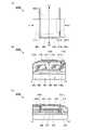
<金属酸化物の構成>
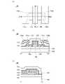
本発明におけるCAC(Cloud-Aligned composite)構成を有す
る金属酸化物の概念図を図1に示す。なお、本明細書において、本発明の一態様である金
属酸化物が、半導体の機能を有する場合、CAC(Cloud-Alignedcomp
osite)-OS(OxideSemiconductor)と定義する。<Composition of metal oxide>
FIG. 1 shows a conceptual diagram of a metal oxide having a CAC (Cloud-Aligned compete) configuration in the present invention. In the present specification, when the metal oxide according to one aspect of the present invention has a semiconductor function, CAC (Cloud-Indexedcomp) is used.
It is defined as (osite) -OS (OxideSemiconductor).
CAC-OSとは、例えば、図1に示すように、金属酸化物を構成する元素が偏在するこ
とで、各元素を主成分とする領域001、および領域002を形成し、各領域が、混合し
、モザイク状に形成される。つまり、金属酸化物を構成する元素が、0.5nm以上10
nm以下、好ましくは、1nm以上2nm以下、またはその近傍のサイズで偏在した材料
の一構成である。なお、以下では、金属酸化物において、一つあるいはそれ以上の金属元
素が偏在し、該金属元素を有する領域が、0.5nm以上10nm以下、好ましくは、1
nm以上2nm以下、またはその近傍のサイズで混合した状態をモザイク状、またはパッ
チ状ともいう。With CAC-OS, for example, as shown in FIG. 1, the elements constituting the metal oxide are unevenly distributed to form a
It is a composition of a material unevenly distributed in a size of nm or less, preferably 1 nm or more and 2 nm or less, or in the vicinity thereof. In the following, in the metal oxide, one or more metal elements are unevenly distributed, and the region having the metal element is 0.5 nm or more and 10 nm or less, preferably 1.
A state in which the mixture is in a size of nm or more and 2 nm or less or in the vicinity thereof is also referred to as a mosaic shape or a patch shape.
例えば、CAC構成を有するIn-M-Zn酸化物とは、インジウム酸化物(以下、In
OX1(X1は0よりも大きい実数)とする。)、またはインジウム亜鉛酸化物(以下、
InX2ZnY2OZ2(X2、Y2、およびZ2は0よりも大きい実数)とする。)と
、元素Mを含む酸化物などと、に材料が分離することでモザイク状となり、モザイク状の
InOX1、またはInX2ZnY2OZ2が、膜中に分布した構成(以下、クラウド状
ともいう。)である。For example, the In—M—Zn oxide having a CAC configuration is an indium oxide (hereinafter, In).
Let it be OX1 (X1 is a real number larger than 0). ), Or indium zinc oxide (hereinafter,
InX2 ZnY2 OZ2 (X2, Y2, and Z2 are real numbers larger than 0). ) And an oxide containing the element M, etc., to form a mosaic, and the mosaic-like InOX1 or InX2 ZnY2OZ2 is distributed in the film (hereinafter, also referred to as cloud-like). It is said.).
別言すると、本発明の一態様の金属酸化物は、In酸化物、In-M酸化物、M酸化物、
MーZn酸化物、In-Zn酸化物、及びIn-M-Zn酸化物の中から選ばれた、少な
くとも2以上の複数の酸化物または複数の材料を有する。In other words, the metal oxide of one aspect of the present invention includes In oxide, In-M oxide, M oxide, and the like.
It has at least two or more oxides or materials selected from M-Zn oxides, In-Zn oxides, and In-M-Zn oxides.
代表的には、本発明の一態様の金属酸化物は、In酸化物、In-Zn酸化物、In-A
l-Zn酸化物、In-Ga-Zn酸化物、In-Y-Zn酸化物、In-Cu-Zn酸
化物、In-V-Zn酸化物、In-Be-Zn酸化物、In-B-Zn酸化物、In-
Si-Zn酸化物、In-Ti-Zn酸化物、In-Fe-Zn酸化物、In-Ni-Z
n酸化物、In-Ge-Zn酸化物、In-Zr-Zn酸化物、In-Mo-Zn酸化物
、In-La-Zn酸化物、In-Ce-Zn酸化物、In-Nd-Zn酸化物、In-
Hf-Zn酸化物、In-Ta-Zn酸化物、In-W-Zn酸化物、及びIn-Mg-
Zn酸化物の中から選ばれた、少なくとも2以上を有する。すなわち、本発明の一態様の
金属酸化物を、複数の材料または複数の成分を有する複合金属酸化物ともいえる。Typically, the metal oxide of one aspect of the present invention is In oxide, In—Zn oxide, In—A.
l-Zn oxide, In-Ga-Zn oxide, In-Y-Zn oxide, In-Cu-Zn oxide, In-V-Zn oxide, In-Be-Zn oxide, In-B- Zn oxide, In-
Si-Zn oxide, In-Ti-Zn oxide, In-Fe-Zn oxide, In-Ni-Z
n-oxide, In-Ge-Zn oxide, In-Zr-Zn oxide, In-Mo-Zn oxide, In-La-Zn oxide, In-Ce-Zn oxide, In-Nd-Zn oxidation Thing, In-
Hf-Zn Oxide, In-Ta-Zn Oxide, In-W-Zn Oxide, and In-Mg-
It has at least 2 or more selected from Zn oxides. That is, the metal oxide of one aspect of the present invention can be said to be a composite metal oxide having a plurality of materials or a plurality of components.
ここで、図1に示す概念が、CAC構成を有するIn-M-Zn酸化物であると仮定する
。その場合、領域001が元素Mを含む酸化物を主成分とする領域、また、領域002が
InX2ZnY2OZ2、またはInOX1を主成分とする領域であるといえる。このと
き、元素Mを含む酸化物が主成分である領域と、InX2ZnY2OZ2、またはInO
X1が主成分である領域と、少なくともZnを有する領域とは、周辺部が不明瞭である(
ボケている)ため、それぞれ明確な境界が観察できない場合がある。Here, it is assumed that the concept shown in FIG. 1 is an In—M—Zn oxide having a CAC configuration. In that case, it can be said that the
The peripheral portion of the region containingX1 as the main component and the region containing at least Zn is unclear (
Because it is out of focus), it may not be possible to observe clear boundaries.
つまり、CAC構成を有するIn-M-Zn酸化物は、元素Mを含む酸化物が主成分であ
る領域と、InX2ZnY2OZ2、またはInOX1が主成分である領域とが、混合し
ている金属酸化物である。従って、金属酸化物を複合金属酸化物と記載する場合がある。
なお、本明細書において、例えば、領域002の元素Mに対するInの原子数比が、領域
001の元素Mに対するInの原子数比よりも大きいことを、領域002は、領域001
と比較して、Inの濃度が高いとする。That is, in the In—M—Zn oxide having a CAC configuration, a region containing an oxide containing an element M as a main component and a region containing InX2 ZnY2 OZ2 or In OX1 as a main component are mixed. It is a metal oxide. Therefore, the metal oxide may be referred to as a composite metal oxide.
In the present specification, for example, the
It is assumed that the concentration of In is higher than that of.
なお、CAC構成を有する金属酸化物とは、組成の異なる二種類以上の膜の積層構造は含
まないものとする。例えば、Inを主成分とする膜と、元素Mを含む酸化物を主成分とす
る膜との2層からなる構造は、含まない。The metal oxide having a CAC structure does not include a laminated structure of two or more types of films having different compositions. For example, it does not include a structure consisting of two layers, a film containing In as a main component and a film containing an oxide containing an element M as a main component.
また、CAC構成において、結晶構造は副次的な要素である。従って、CAC構成を有す
るIn-M-Zn酸化物において、領域001、および領域002における結晶構造は、
特に限定されない。また、領域001、および領域002は、それぞれ、異なる結晶構造
を有していてもよい。Also, in the CAC configuration, the crystal structure is a secondary element. Therefore, in the In—M—Zn oxide having a CAC configuration, the crystal structure in the
Not particularly limited. Further, the
例えば、CAC構成を有するIn-M-Zn酸化物において、非単結晶構造を有する酸化
物半導体であることが好ましい。非単結晶構造として、例えば、CAAC-OS、多結晶
酸化物半導体、nc-OS(nanocrystallineoxidesemicon
ductor)、擬似非晶質酸化物半導体(a-likeOS:amorphous-l
ikeoxidesemiconductor)および非晶質酸化物半導体などがある。For example, in the In—M—Zn oxide having a CAC structure, an oxide semiconductor having a non-single crystal structure is preferable. As a non-single crystal structure, for example, CAAC-OS, polycrystalline oxide semiconductor, nc-OS (nanocrystallineoxidesemicon)
ductor), pseudo-amorphous oxide semiconductor (a-likeOS: amorphous-l)
There are ikeoxidesemiconductor) and amorphous oxide semiconductors.
なお、CAAC-OSは、CAAC構造を有する。CAAC構造とは、c軸配向性を有し
、かつa-b面方向において複数のナノ結晶が連結し、歪みを有した結晶構造の酸化物半
導体である。なお、歪みとは、複数のナノ結晶が連結する領域において、格子配列の揃っ
た領域と、別の格子配列の揃った領域と、の間で格子配列の向きが変化している箇所を指
す。The CAAC-OS has a CAAC structure. The CAAC structure is an oxide semiconductor having a c-axis orientation and a crystal structure in which a plurality of nanocrystals are connected in the ab plane direction and has strain. The strain refers to a region where the orientation of the lattice arrangement changes between a region in which the lattice arrangement is aligned and a region in which another lattice arrangement is aligned in the region where a plurality of nanocrystals are connected.
ナノ結晶は、六角形を基本とするが、正六角形状とは限らず、非正六角形状である場合が
ある。また、歪みにおいて、五角形、および七角形などの格子配列を有する場合がある。
従って、CAAC-OSにおいて、歪み近傍においても、明確な結晶粒界(グレインバウ
ンダリーともいう)を確認することはできない。即ち、格子配列の歪みによって、結晶粒
界の形成が抑制されていることがわかる。これは、CAAC-OSが、a-b面方向にお
いて、酸素原子の配列が稠密でないことや、金属元素が置換することで原子間の結合距離
が変化することなどによって、歪みを許容することができるためと考えられる。Although nanocrystals are basically hexagonal, they are not limited to regular hexagonal shapes and may have non-regular hexagonal shapes. In addition, in distortion, it may have a lattice arrangement such as a pentagon and a heptagon.
Therefore, in CAAC-OS, a clear grain boundary (also referred to as grain boundary) cannot be confirmed even in the vicinity of strain. That is, it can be seen that the formation of grain boundaries is suppressed by the distortion of the lattice arrangement. This is because CAAC-OS allows distortion due to the fact that the arrangement of oxygen atoms is not dense in the ab plane direction and that the bond distance between atoms changes due to the substitution of metal elements. It is thought that it can be done.
nc-OSは、微小な領域(例えば、1nm以上10nm以下の領域、特に1nm以上3
nm以下の領域)において原子配列に周期性を有する。また、nc-OSは、異なるナノ
結晶間で結晶方位に規則性が見られない。そのため、膜全体で配向性が見られない。した
がって、nc-OSは、分析方法によっては、a-likeOSや非晶質酸化物半導体と
区別が付かない場合がある。The nc-OS is a minute region (for example, a region of 1 nm or more and 10 nm or less, particularly a region of 1 nm or more and 3).
The atomic arrangement has periodicity in the region below nm). In addition, nc-OS has no regularity in crystal orientation between different nanocrystals. Therefore, no orientation is observed in the entire film. Therefore, nc-OS may be indistinguishable from a-like OS and amorphous oxide semiconductors depending on the analysis method.
a-likeOSは、nc-OSと非晶質酸化物半導体との間の構造を有する酸化物半導
体である。a-likeOSは、鬆または低密度領域を有する。即ち、a-likeOS
は、nc-OSおよびCAAC-OSと比べて、不安定な構造である。The a-likeOS is an oxide semiconductor having a structure between nc-OS and an amorphous oxide semiconductor. The a-likeOS has a void or low density region. That is, a-likeOS
Has an unstable structure as compared with nc-OS and CAAC-OS.
例えば、CAC-OSは、CAAC構造を有することが好ましい。CAAC構造は、領域
001、または領域002を含む範囲で形成される場合がある。つまり、CAC-OSに
おいて、CAAC-OSとなる領域は、数nmから数十nmの範囲で形成される。For example, the CAC-OS preferably has a CAAC structure. The CAAC structure may be formed in a
CAAC-OSは結晶性の高い酸化物半導体である。一方、CAAC-OSは、明確な結
晶粒界を確認することはできないため、結晶粒界に起因する電子移動度の低下が起こりに
くいといえる。従って、CAAC-OSを有することで、金属酸化物としての物理的性質
が安定するため、熱に強く、信頼性が高い金属酸化物を提供することができる。CAAC-OS is a highly crystalline oxide semiconductor. On the other hand, in CAAC-OS, since a clear crystal grain boundary cannot be confirmed, it can be said that the decrease in electron mobility due to the crystal grain boundary is unlikely to occur. Therefore, by having CAAC-OS, the physical properties of the metal oxide are stabilized, so that it is possible to provide a metal oxide that is resistant to heat and has high reliability.
具体的には、In-Ga-Zn酸化物におけるCAC-OS(なお、CAC-OSの中で
もIn-Ga-Zn酸化物を、特にCAC-IGZOと呼称してもよい。)について説明
する。In-Ga-Zn酸化物におけるCAC-OSは、InOX1、またはInX2Z
nY2OZ2と、インジウムガリウム亜鉛酸化物(以下、InaGabZncOd(a、
b、c、およびd0よりも大きい実数)とする。)などと、に材料が分離することでモザ
イク状となり、モザイク状のInOX1、またはInX2ZnY2OZ2がクラウド状で
ある金属酸化物である。Specifically, CAC-OS in In-Ga-Zn oxide (Note that In-Ga-Zn oxide may be particularly referred to as CAC-IGZO among CAC-OS) will be described. CAC-OS in In-Ga-Zn oxide is InOX1 or InX2 Z.
nY2 OZ2 and indium gallium zinc oxide (hereinafter referred to as Ina Gab ZncOd (a,
b, c, and a real number larger than d0). ) And the like, and the material is separated to form a mosaic, and the mosaic-like InOX1 or InX2 ZnY2 OZ2 is a cloud-like metal oxide.
つまり、In-Ga-Zn酸化物におけるCAC-OSは、InaGabZncOdが主
成分である領域と、InX2ZnY2OZ2、またはInOX1が主成分である領域とが
、混合している構成を有する複合金属酸化物である。また、InaGabZncOdが主
成分である領域と、InX2ZnY2OZ2、またはInOX1が主成分である領域とは
、周辺部が不明瞭である(ボケている)ため、明確な境界が観察できない場合がある。That is, in the CAC-OS in the In-Ga-Zn oxide, the region in which Ina Gab ZncOd is the main component and the region in which InX2 ZnY2 OZ2 or In OX1 is the main component are formed. It is a composite metal oxide having a mixed composition. Further, the peripheral portion of the region where Ina Gab ZncOd is the main component and the region where InX2 ZnY2 OZ2 or InOX1 is the main component is unclear (blurred). , Clear boundaries may not be observable.
例えば、図1に示す概念図において、領域001がInaGabZncOdを主成分とす
る領域に相当し、領域002がInX2ZnY2OZ2、またはInOX1を主成分とす
る領域に相当する。なお、InaGabZncOdを主成分とする領域、及びInX2Z
nY2OZ2、またはInOX1を主成分とする領域を、それぞれナノ粒子と呼称しても
よい。当該ナノ粒子は、粒子の径が0.5nm以上10nm以下、代表的には1nm以上
2nm以下である。また、上記ナノ粒子は、周辺部が不明瞭である(ボケている)ため、
明確な境界が観察できない場合がある。For example, in the conceptual diagram shown in FIG. 1, the
The regions containing nY2 OZ2 or InOX1 as main components may be referred to as nanoparticles. The nanoparticles have a particle diameter of 0.5 nm or more and 10 nm or less, typically 1 nm or more and 2 nm or less. In addition, since the peripheral part of the nanoparticles is unclear (blurred),
Clear boundaries may not be observable.
なお、領域001、および領域002のサイズは、エネルギー分散型X線分光法(EDX
:EnergyDispersiveX-rayspectroscopy)を用いて取
得したEDXマッピングで評価することができる。例えば、領域001は、断面写真のE
DXマッピングにおいて、領域001の径が、0.5nm以上10nm以下、または1n
m以上2nm以下で観察される場合がある。また、領域の中心部から周辺部にかけて、主
成分である元素の密度は、徐々に小さくなる。例えば、EDXマッピングでカウントでき
る元素の個数(以下、存在量ともいう)が、中心部から周辺部に向けて傾斜すると、断面
写真のEDXマッピングにおいて、領域の周辺部が不明瞭な(ボケた)状態で観察される
。例えば、InaGabZncOdが主成分である領域において、Ga原子は、中心部か
ら周辺部にかけて徐々に減少し、代わりに、In原子、およびZn原子が増加することで
、InX2ZnY2OZ2が主成分である領域へと段階的に変化する。従って、EDXマ
ッピングにおいて、InaGabZncOdが主成分である領域の周辺部は不明瞭な(ボ
ケた)状態で観察される。The sizes of
: EnergyDispersiveX-rayspectropy) can be evaluated by EDX mapping acquired. For example, the
In DX mapping, the diameter of
It may be observed at m or more and 2 nm or less. Further, the density of the element as the main component gradually decreases from the central portion to the peripheral portion of the region. For example, when the number of elements that can be counted by EDX mapping (hereinafter, also referred to as abundance) is inclined from the central part toward the peripheral part, the peripheral part of the region is unclear (blurred) in the EDX mapping of the cross-sectional photograph. Observed in the state. For example, in the region where Ina Gab ZncOd is the main component, the Ga atom gradually decreases from the central part to the peripheral part, and instead, the In atom and the Zn atom increase, so that InX2 It gradually changes to the region where ZnY2 OZ2 is the main component. Therefore, in the EDX mapping, the peripheral portion of the region in which Ina Gab ZncOd is the main component is observed in an unclear (blurred) state.
なお、CAC構成を有するIn-Ga-Zn酸化物における結晶構造は、特に限定されな
い。また、領域001、および領域002は、それぞれ、異なる結晶構造を有していても
よい。The crystal structure of the In—Ga—Zn oxide having a CAC structure is not particularly limited. Further, the
ここで、In-Ga-Zn-O系の金属酸化物をIGZOと示す場合があるが、IGZO
は通称であり、In、Ga、Zn、およびOによる1つの化合物をいう場合がある。In
-Ga-Zn-O系の金属酸化物の一例としては、結晶性の化合物が挙げられる。結晶性
の化合物は、単結晶構造、多結晶構造、またはCAAC(c-axisalignedc
rystalline)構造を有する。なお、CAAC構造とは、複数のIGZOのナノ
結晶がc軸配向を有し、かつa-b面においては配向せずに連結した層状の結晶構造であ
る。Here, the In—Ga—Zn—O-based metal oxide may be referred to as IGZO, but IGZO
Is a common name and may refer to one compound of In, Ga, Zn, and O. In
An example of a -Ga—Zn—O based metal oxide is a crystalline compound. Crystalline compounds can be single crystal, polycrystalline, or CAAC (c-axisalignedc).
It has a rystalline) structure. The CAAC structure is a layered crystal structure in which a plurality of IGZO nanocrystals have a c-axis orientation and are connected without being oriented on the ab plane.
例えば、CAC構成を有するIn-Ga-Zn酸化物は、非単結晶構造を有する酸化物半
導体であることが好ましい。特に、CAC構成を有するIn-Ga-Zn酸化物は、CA
AC-IGZOを有することが好ましい。また、CAAC-IGZOとなる範囲には、領
域001を有することが好ましい。CAAC-IGZOを有することで、金属酸化物とし
ての物理的性質が安定するため、熱に強く、信頼性が高いIn-Ga-Zn酸化物を提供
することができる。For example, the In—Ga—Zn oxide having a CAC structure is preferably an oxide semiconductor having a non-single crystal structure. In particular, the In-Ga-Zn oxide having a CAC configuration is CA.
It is preferable to have AC-IGZO. Further, it is preferable to have
なお、In-Ga-Zn酸化物におけるCAC-OSにおける結晶性は、電子線回折で評
価することができる。例えば、電子線回折パターン像において、リング状に輝度の高い領
域、およびリング状に輝度の高い領域内に、複数のスポットが観察される場合がある。The crystallinity of In-Ga-Zn oxide in CAC-OS can be evaluated by electron diffraction. For example, in the electron diffraction pattern image, a plurality of spots may be observed in a ring-shaped high-luminance region and a ring-shaped high-luminance region.
ここで、InX2ZnY2OZ2、またはInOX1が主成分である領域は、InaGa
bZncOdなどが主成分である領域と比較して、導電性が高い領域である。つまり、I
nX2ZnY2OZ2、またはInOX1が主成分である領域を、キャリアが流れること
により、酸化物半導体としての導電性が発現する。従って、InX2ZnY2OZ2、ま
たはInOX1が主成分である領域が、酸化物半導体中にクラウド状に分布することで、
高い電界効果移動度(μ)が実現できる。なお、InX2ZnY2OZ2、またはInO
X1が主成分である領域は、導電体の性質に近い、半導体の領域ともいえる。Here, the region in which InX2 ZnY2 OZ2 or InOX1 is the main component is Ina Ga.
b This is a region having high conductivity as compared with the region in which ZncOd or the like is the main component. That is, I
When a carrier flows through a region containing nX2 ZnY2 OZ2 or InOX1 as a main component, conductivity as an oxide semiconductor is exhibited. Therefore, the region containing InX2 ZnY2 OZ2 or InOX1 as the main component is distributed in the oxide semiconductor in a cloud shape.
High field effect mobility (μ) can be realized. InX2 ZnY2 OZ2 or InO
The region in whichX1 is the main component can be said to be a semiconductor region that is close to the properties of a conductor.
一方、InaGabZncOdなどが主成分である領域は、InX2ZnY2OZ2、ま
たはInOX1が主成分である領域と比較して、導電性が低い領域である。つまり、In
aGabZncOdなどが主成分である領域が、金属酸化物中に分布することで、リーク
電流を抑制し、良好なスイッチング動作を実現できる。なお、InaGabZncOdな
どが主成分である領域は、絶縁体の性質に近い、半導体の領域ともいえる。On the other hand, the region in which Ina Gab ZncOd or the like is the main component is a region having lower conductivity than the region in which InX2 ZnY2 OZ2 or InOX1 is the main component. In other words, In
Since the region containinga Gab ZncOd or the like as a main component is distributed in the metal oxide, leakage current can be suppressed and good switching operation can be realized. It should be noted that the region in which Ina Gab ZncOd or the like is the main component can be said to be a semiconductor region close to the properties of an insulator.
従って、In-Ga-Zn酸化物におけるCAC-OSを半導体素子に用いた場合、In
aGabZncOdなどに起因する性質と、InX2ZnY2OZ2、またはInOX1
に起因する性質とが、相補的に作用することにより、高いオン電流(Ion)、高い電界
効果移動度(μ)、および、低いオフ電流(Ioff)を実現することができる。Therefore, when CAC-OS in In-Ga-Zn oxide is used for the semiconductor element, In
Properties caused bya Gab ZncOd , etc., and InX2 ZnY2 OZ2 , or In OX1
By complementing the properties caused by the above, high on-current (Ion ), high field-effect mobility (μ), and low off-current (Ioff ) can be realized.
また、In-Ga-Zn酸化物におけるCAC-OSを用いた半導体素子は、信頼性が高
い。従って、In-Ga-Zn酸化物におけるCAC-OSは、ディスプレイをはじめと
するさまざまな半導体装置に最適である。Further, the semiconductor device using CAC-OS in In—Ga—Zn oxide has high reliability. Therefore, CAC-OS in In-Ga-Zn oxide is most suitable for various semiconductor devices such as displays.
<金属酸化物を有するトランジスタ>
続いて、上記金属酸化物を半導体としてトランジスタに用いる場合について説明する。<Transistor with metal oxide>
Subsequently, a case where the metal oxide is used as a semiconductor in a transistor will be described.
なお、上記金属酸化物を半導体としてトランジスタに用いることで、電界効果移動度が高
く、かつ、スイッチング特性が高いトランジスタを実現することができる。また、信頼性
の高いトランジスタを実現することができる。By using the metal oxide as a semiconductor in a transistor, it is possible to realize a transistor having high field effect mobility and high switching characteristics. In addition, a highly reliable transistor can be realized.
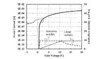
図2(A)は、上記金属酸化物をチャネル形成領域に用いたトランジスタの模式図である
。図2(A)において、トランジスタは、ソースと、ドレインと、第1のゲートと、第2
のゲートと、第1のゲート絶縁部と、第2のゲート絶縁部と、チャネル部と、を有する。
トランジスタは、ゲートに印加する電位によって、チャネル部の抵抗を制御することがで
きる。即ち、第1のゲート、または第2のゲートに印加する電位によって、ソースとドレ
インとの間の導通(トランジスタがオン状態)・非導通(トランジスタがオフ状態)を制
御することができる。FIG. 2A is a schematic diagram of a transistor using the metal oxide in the channel forming region. In FIG. 2A, the transistor has a source, a drain, a first gate, and a second.
It has a gate, a first gate insulating portion, a second gate insulating portion, and a channel portion.
The transistor can control the resistance of the channel portion by the potential applied to the gate. That is, conduction (transistor is on) and non-conduction (transistor is off) between the source and the drain can be controlled by the potential applied to the first gate or the second gate.
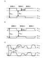
ここで、チャネル部は、第1のバンドギャップを有する領域001と、第2のバンドギャ
ップを有する領域002と、がクラウド状であるCAC-OSを有している。なお、第1
のバンドギャップは、第2のバンドギャップよりも大きいものとする。Here, the channel portion has a CAC-OS in which a
The bandgap of is larger than the second bandgap.
例えば、チャネル部のCAC-OSとして、CAC構成を有するIn-Ga-Zn酸化物
を用いる場合について説明する。CAC構成を有するIn-Ga-Zn酸化物は、領域0
01として、領域002よりもGaの濃度が高いInaGabZncOdを主成分とする
領域と、領域002として、領域001よりもInの濃度が高いInX2ZnY2OZ2
、またはInOX1が主成分である領域と、に材料が分離することでモザイク状となり、
InOX1、またはInX2ZnY2OZ2が、膜中に分布した構成(クラウド状)であ
る。なお、InaGabZncOdを主成分とする領域001は、InX2ZnY2OZ
2、またはInOX1が主成分である領域002よりも、大きなバンドギャップを有する
。For example, a case where an In-Ga-Zn oxide having a CAC configuration is used as the CAC-OS of the channel portion will be described. The In-Ga-Zn oxide having a CAC configuration has
As 01, a region whose main component is Ina Gab ZncOd , which has a higher concentration of Ga than
, Or the region where InOX1 is the main component, and the material separates into a mosaic.
InOX1 or InX2 ZnY2 OZ2 is distributed in the film (cloud-like). The
2 or has a larger bandgap than the
ここで、CAC-OSをチャネル部に有する図2(A)に示すトランジスタの伝導モデル
について説明する。図2(B)は、図2(A)に示すトランジスタのソースとドレインと
の間におけるエネルギー準位の分布を説明する模式図である。また、図2(C)は、図2
(A)に示すトランジスタにおいて、X-X’で示す実線上における伝導バンド図である
。なお、各伝導帯において、実線は伝導帯下端のエネルギーを示す。また、Efで示す一
点破線は電子の擬フェルミ準位のエネルギーを示す。また、ここでは、第1のゲート電圧
として、ゲートとソースとの間にマイナスの電圧を印加し、ソースとドレインとの間にド
レイン電圧(Vd>0)を印加している。Here, a conduction model of the transistor shown in FIG. 2A having a CAC-OS in the channel portion will be described. FIG. 2B is a schematic diagram illustrating the distribution of energy levels between the source and drain of the transistor shown in FIG. 2A. Further, FIG. 2 (C) is shown in FIG.
In the transistor shown in (A), it is a conduction band diagram on the solid line shown by XX'. In each conduction band, the solid line indicates the energy at the lower end of the conduction band. The one-dot dashed line indicated by Ef indicates the energy of the quasi-Fermi level of the electron. Further, here, as the first gate voltage, a negative voltage is applied between the gate and the source, and a drain voltage (Vd > 0) is applied between the source and the drain.
図2(A)に示すトランジスタに、マイナスのゲート電圧を印加すると、図2(B)に示
すように、ソースとドレインとの間に、領域001に由来する伝導帯CB001と、領域
002に由来する伝導帯CB002と、が形成される。ここで、第1のバンドギャップは
第2のバンドギャップよりも大きいため、伝導帯CB001におけるポテンシャル障壁は
、伝導帯CB002のポテンシャル障壁よりも大きい。つまり、チャネル部におけるポテ
ンシャル障壁の最大値は、領域001に起因する値をとる。従って、CAC-OSをチャ
ネル部に用いることで、リーク電流を抑制し、スイッチング特性が高いトランジスタとす
ることができる。When a negative gate voltage is applied to the transistor shown in FIG. 2 (A), as shown in FIG. 2 (B), the conduction band CB001 derived from the
また、図2(C)に示すように、第1のバンドギャップを有する領域001は、第2のバ
ンドギャップを有する領域002より、バンドギャップが相対的に広いので、第1のバン
ドギャップを有する領域のEc端は、第2のバンドギャップを有する領域のEc端よりも
相対的に高い位置に存在しうる。Further, as shown in FIG. 2C, the
例えば、第1のバンドギャップを有する領域001の成分が、In-Ga-Zn酸化物(
In:Ga:Zn=1:1:1[原子数比])であり、第2のバンドギャップを有する領
域002の成分がIn-Zn酸化物(In:Zn=2:3[原子数比])である場合を仮
定する。この場合、第1のバンドギャップは、3.3eV、またはその近傍であり、第2
のバンドギャップは、2.4eV、またはその近傍となる。なお、バンドギャップの値は
、各材料の単膜をエリプソメータで測定して得られる値を用いる。For example, the component of
In: Ga: Zn = 1: 1: 1 [atomic number ratio]), and the component of
The bandgap of is 2.4 eV or its vicinity. As the bandgap value, a value obtained by measuring a single film of each material with an ellipsometer is used.
上記の仮定の場合、第1のバンドギャップと、第2のバンドギャップとの差は0.9eV
である。本発明の一態様においては、第1のバンドギャップと、第2のバンドギャップと
の差は、少なくとも0.1eV以上あればよい。ただし、第1のバンドギャップを有する
領域001に由来する価電子帯VB001の位置と、第2のバンドギャップを有する領域
002に由来する価電子帯VB002の位置が異なる場合があるので、第1のバンドギャ
ップと、第2のバンドギャップとの差が、好ましくは0.3eV以上、さらに好ましくは
0.4eV以上であるとよい。In the case of the above assumption, the difference between the first bandgap and the second bandgap is 0.9 eV.
Is. In one aspect of the present invention, the difference between the first bandgap and the second bandgap may be at least 0.1 eV or more. However, the position of the valence band VB001 derived from the
また、上記の仮定の場合、CAC-OS中にキャリアを流れる際に、第2のバンドギャッ
プ、すなわちナローバンドであるIn-Zn酸化物に起因してキャリアが流れる。この際
に、第2のバンドギャップから第1のバンドギャップ、すなわちワイドバンドであるIn
-Ga-Zn酸化物側にキャリアが溢れる。別言すると、ナローバンドであるIn-Zn
酸化物の方がキャリアを生成しやすく、当該キャリアは、ワイドバンドであるIn-Ga
-Zn酸化物に移動する。Further, in the case of the above assumption, when the carrier flows in the CAC-OS, the carrier flows due to the second band gap, that is, the narrow band In—Zn oxide. At this time, the second bandgap to the first bandgap, that is, the wide band In.
-Carriers overflow on the Ga-Zn oxide side. In other words, the narrow band In-Zn
Oxides are more likely to generate carriers, which are wideband In-Ga.
-Move to Zn oxide.
なお、チャネル部を形成する金属酸化物中において、領域001と、領域002とは、モ
ザイク状であり、領域001、および領域002は不規則に偏在している。そのため、X
-X’で示す実線上における伝導バンド図は一例である。In the metal oxide forming the channel portion, the
The conduction band diagram on the solid line indicated by -X'is an example.
基本的に、図3(A)に示すように、領域002が領域001に挟まれたバンドを形成し
ていればよい。または、領域001が領域002に挟まれたバンドを形成していればよい
。Basically, as shown in FIG. 3A, the
また、実際のCAC-OSでは、第1のバンドギャップを有する領域001と第2のバン
ドギャップを有する領域002との接合部は、領域の凝集形態や組成に揺らぎが生じてい
ると考えられる。従って、図3(B)、および図3(C)に示すように、バンドは不連続
ではなく、連続的に変化している場合がある。すなわち、CAC-OS中にキャリアが流
れる際に、第1のバンドギャップと、第2のバンドギャップとが連動すると言い換えても
良い。Further, in an actual CAC-OS, it is considered that the agglomeration form and composition of the region at the junction between the
図4に、図2(A)に示すトランジスタおいて、X-X’で示す実線上における概略バン
ドダイアグラムのモデルを示す。なお、第1のゲート電極に電圧を印加する場合、第2の
ゲート電極にも同じ電圧を同時に印加している。図4(A)には、第1のゲート電圧Vg
として、ゲートとソースとの間にプラスの電圧(Vg>0)を印加した状態(ONSta
te)を示す。図4(B)には、第1のゲート電圧Vgを印加しない(Vg=0)状態を
示す。図4(C)には、第1のゲート電圧Vgとして、ゲートとソースとの間にマイナス
の電圧(Vg<0)を印加した状態(OFFState)を示す。なお、各伝導帯におい
て、実線は伝導帯下端のエネルギーを示す。また、Efで示す一点鎖線は電子の擬フェル
ミ準位のエネルギーを示す。FIG. 4 shows a model of a schematic band diagram on a solid line indicated by XX'in the transistor shown in FIG. 2 (A). When a voltage is applied to the first gate electrode, the same voltage is also applied to the second gate electrode at the same time. FIG. 4 (A) shows the first gate voltage Vg .
As a result, a positive voltage (Vg > 0) is applied between the gate and the source (ONSta).
te) is shown. FIG. 4B shows a state in which the first gate voltage Vg is not applied (Vg = 0). FIG. 4C shows a state (OFFState) in which a negative voltage (Vg <0) is applied between the gate and the source as the first gate voltage Vg . In each conduction band, the solid line indicates the energy at the lower end of the conduction band. The alternate long and short dash line indicated by Ef indicates the energy of the quasi-Fermi level of electrons.
CAC-OSをチャネル部に有するトランジスタは、第1のバンドギャップを有する領域
001と第2のバンドギャップを有する領域002とが、電気的に相互作用を及ぼす。別
言すると、第1のバンドギャップを有する領域001と第2のバンドギャップを有する領
域002とが、相補的に機能する。In the transistor having CAC-OS in the channel portion, the
図4(A)に示すように、トランジスタをオン状態にする方向の電位(Vg>0)が、第
1のゲート電極に印加されると、Ec端の低い第2のバンドギャップを有する領域002
が主な伝導経路となり、電子が流れると同時に、第1のバンドギャップを有する領域00
1にも電子が流れる。このためトランジスタのオン状態において高い電流駆動力、つまり
大きなオン電流および高い電界効果移動度を得ることができる。As shown in FIG. 4A, when a potential (Vg > 0) in the direction of turning on the transistor is applied to the first gate electrode, a region having a second band gap with a low Ec end is applied. 002
Is the main conduction path, and at the same time as the electrons flow, the
Electrons also flow in 1. Therefore, a high current driving force, that is, a large on-current and a high field effect mobility can be obtained in the on state of the transistor.
一方、図4(B)、および図4(C)に示すように、第1のゲートにしきい値電圧未満の
電圧(Vg≦0)を印加することで、第1バンドギャップを有する領域001は、誘電体
(絶縁体)として振る舞うので、領域001中の伝導経路は遮断される。また、第2のバ
ンドギャップを有する領域002は、第1のバンドギャップを有する領域001と接して
いる。従って、第1のバンドギャップを有する領域001は、自らに加えて第2のバンド
ギャップを有する領域002へ電気的に相互作用を及ぼし、第2のバンドギャップを有す
る領域002中の伝導経路すらも遮断する。これでチャネル部全体が非導通状態となり、
トランジスタはオフ状態となる。On the other hand, as shown in FIGS. 4 (B) and 4 (C), by applying a voltage (Vg ≦ 0) less than the threshold voltage to the first gate, the
The transistor is turned off.
以上より、トランジスタにCAC-OSを用いることで、トランジスタの動作時、例えば
、ゲートと、ソースまたはドレインとの間に電位差が生じた時に、ゲートと、ソースまた
はドレインと、の間のリーク電流を低減または防止することができる。From the above, by using CAC-OS for the transistor, the leakage current between the gate and the source or drain can be generated when the transistor is operating, for example, when a potential difference occurs between the gate and the source or drain. Can be reduced or prevented.
また、トランジスタには、キャリア密度の低い半導体を用いることが好ましい。高純度真
性または実質的に高純度真性である金属酸化物は、キャリア発生源が少ないため、キャリ
ア密度を低くすることができる。また、高純度真性または実質的に高純度真性である金属
酸化物は、欠陥準位密度が低いため、トラップ準位密度も低くなる場合がある。Further, it is preferable to use a semiconductor having a low carrier density for the transistor. Metal oxides of high purity or substantially high purity can have low carrier densities due to the small number of carrier sources. In addition, metal oxides having high-purity intrinsics or substantially high-purity intrinsics have a low defect level density, so that the trap level density may also be low.
また、金属酸化物のトラップ準位に捕獲された電荷は、消失するまでに要する時間が長く
、あたかも固定電荷のように振る舞うことがある。そのため、トラップ準位密度の高い金
属酸化物にチャネル形成領域が形成されるトランジスタは、電気特性が不安定となる場合
がある。In addition, the charge captured at the trap level of the metal oxide takes a long time to disappear, and may behave as if it were a fixed charge. Therefore, a transistor in which a channel forming region is formed in a metal oxide having a high trap level density may have unstable electrical characteristics.
従って、トランジスタの電気特性を安定にするためには、金属酸化物中の不純物濃度を低
減することが有効である。また、金属酸化物中の不純物濃度を低減するためには、近接す
る膜中の不純物濃度も低減することが好ましい。不純物としては、水素、アルカリ金属、
アルカリ土類金属、鉄、ニッケル、シリコン等がある。Therefore, in order to stabilize the electrical characteristics of the transistor, it is effective to reduce the concentration of impurities in the metal oxide. Further, in order to reduce the impurity concentration in the metal oxide, it is preferable to reduce the impurity concentration in the adjacent film. Impurities include hydrogen, alkali metals,
There are alkaline earth metals, iron, nickel, silicon, etc.
ここで、金属酸化物中における各不純物の影響について説明する。Here, the influence of each impurity in the metal oxide will be described.
金属酸化物において、第14族元素の一つであるシリコンや炭素が含まれると、金属酸化
物において欠陥準位が形成される。このため、金属酸化物におけるシリコンや炭素の濃度
と、金属酸化物との界面近傍のシリコンや炭素の濃度(二次イオン質量分析法(SIMS
:Secondary Ion Mass Spectrometry)により得られる
濃度)を、2×10¹⁸atoms/cm3以下、好ましくは2×1017atoms/
cm3以下とする。When silicon or carbon, which is one of the Group 14 elements, is contained in the metal oxide, a defect level is formed in the metal oxide. Therefore, the concentration of silicon and carbon in the metal oxide and the concentration of silicon and carbon near the interface with the metal oxide (secondary ion mass spectrometry (SIMS)).
: Concentration obtained by Secondary Ion Mass Spectrometry)) is 2 × 10¹⁸ atoms / cm3 or less, preferably 2 × 10¹⁷ atoms /.
It shall be cm3 or less.
また、金属酸化物にアルカリ金属またはアルカリ土類金属が含まれると、欠陥準位を形成
し、キャリアを生成する場合がある。従って、アルカリ金属またはアルカリ土類金属が含
まれている金属酸化物を用いたトランジスタはノーマリーオン特性となりやすい。このた
め、金属酸化物中のアルカリ金属またはアルカリ土類金属の濃度を低減することが好まし
い。具体的には、SIMSにより得られる金属酸化物中のアルカリ金属またはアルカリ土
類金属の濃度を、1×10¹⁸atoms/cm3以下、好ましくは2×1016ato
ms/cm3以下とする。Further, when the metal oxide contains an alkali metal or an alkaline earth metal, it may form a defect level and generate a carrier. Therefore, a transistor using a metal oxide containing an alkali metal or an alkaline earth metal tends to have a normally-on characteristic. Therefore, it is preferable to reduce the concentration of alkali metal or alkaline earth metal in the metal oxide. Specifically, the concentration of the alkali metal or alkaline earth metal in the metal oxide obtained by SIMS is 1 × 10¹⁸ atoms / cm3 or less, preferably 2 × 10¹⁶ atto.
It should be ms / cm3 or less.
また、金属酸化物に含まれる水素は、金属原子と結合する酸素と反応して水になるため、
酸素欠損(Vo)を形成する場合がある。該酸素欠損(Vo)に水素が入ることで、キャ
リアである電子が生成される場合がある。また、水素の一部が金属原子と結合する酸素と
結合して、キャリアである電子を生成することがある。従って、水素が含まれている金属
酸化物を用いたトランジスタはノーマリーオン特性となりやすい。このため、金属酸化物
中の水素はできる限り低減されていることが好ましい。具体的には、金属酸化物において
、SIMSにより得られる水素濃度を、1×10²⁰atoms/cm3未満、好ましく
は1×10¹⁹atoms/cm3未満、より好ましくは5×1018atoms/cm
3未満、さらに好ましくは1×10¹⁸atoms/cm3未満とする。In addition, hydrogen contained in metal oxides reacts with oxygen bonded to metal atoms to become water.
May form oxygen deficiency (Vo ). When hydrogen enters the oxygen deficiency (Vo ), electrons that are carriers may be generated. In addition, a part of hydrogen may be combined with oxygen that is bonded to a metal atom to generate an electron as a carrier. Therefore, a transistor using a metal oxide containing hydrogen tends to have a normally-on characteristic. Therefore, it is preferable that hydrogen in the metal oxide is reduced as much as possible. Specifically, in metal oxides, the hydrogen concentration obtained by SIMS is less than 1 × 10²⁰ atoms / cm3 , preferably less than 1 × 10¹⁹ atoms / cm3 , more preferably 5 × 10¹⁸ atoms / cm.
Less than3 , more preferably less than 1 × 10¹⁸ atoms / cm3 .
なお、金属酸化物中の酸素欠損(Vo)は、酸素を金属酸化物に導入することで、低減す
ることができる。つまり、金属酸化物中の酸素欠損(Vo)に、酸素が補填されることで
、酸素欠損(Vo)は消失する。従って、金属酸化物中に、酸素を拡散させることで、ト
ランジスタの酸素欠損(Vo)を低減し、信頼性を向上させることができる。Oxygen deficiency (Vo ) in the metal oxide can be reduced by introducing oxygen into the metal oxide. That is, the oxygen deficiency (Vo ) in the metal oxide is supplemented with oxygen, so that the oxygen deficiency (Vo ) disappears. Therefore, by diffusing oxygen in the metal oxide, oxygen deficiency (Vo ) of the transistor can be reduced and reliability can be improved.
なお、酸素を金属酸化物に導入する方法として、例えば、金属酸化物に接して、化学量論
的組成を満たす酸素よりも多くの酸素を含む酸化物を設けることができる。つまり、酸化
物には、化学量論的組成よりも酸素が過剰に存在する領域(以下、過剰酸素領域ともいう
)が形成されていることが好ましい。特に、トランジスタに金属酸化物を用いる場合、ト
ランジスタ近傍の下地膜や、層間膜などに、過剰酸素領域を有する酸化物を設けることで
、トランジスタの酸素欠損を低減し、信頼性を向上させることができる。As a method for introducing oxygen into a metal oxide, for example, an oxide containing more oxygen than oxygen satisfying a stoichiometric composition can be provided in contact with the metal oxide. That is, it is preferable that the oxide has a region in which oxygen is excessively present (hereinafter, also referred to as an excess oxygen region) rather than a stoichiometric composition. In particular, when a metal oxide is used for the transistor, oxygen deficiency of the transistor can be reduced and reliability can be improved by providing an oxide having an excess oxygen region in the undercoat film near the transistor and the interlayer film. can.
不純物が十分に低減された金属酸化物をトランジスタのチャネル形成領域に用いることで
、安定した電気特性を付与することができる。By using a metal oxide having sufficiently reduced impurities in the channel forming region of the transistor, stable electrical characteristics can be imparted.
<金属酸化物の成膜方法>
以下では、金属酸化物の一例について説明する。<Metal oxide film formation method>
Hereinafter, an example of the metal oxide will be described.
金属酸化物を成膜する際の温度としては、100℃以上140℃未満とすることが好まし
い。例えばG8等の大型基板は、そのサイズに応じて、基板温度の制限がある。従って、
水の気化温度(100℃以上)より高く、かつ可能な範囲で装置のメンテナビリティー、
スループットの良い温度を適宜選択すればよい。The temperature at which the metal oxide is formed is preferably 100 ° C. or higher and lower than 140 ° C. For example, a large substrate such as G8 has a limitation of the substrate temperature depending on its size. Therefore,
Equipment maintainability higher than water vaporization temperature (100 ° C or higher) and to the extent possible,
A temperature with a good throughput may be selected as appropriate.
また、スパッタリングガスは、希ガス(代表的にはアルゴン)、酸素、希ガス及び酸素の
混合ガスを適宜用いる。混合ガスの場合、成膜ガス全体に占める酸素ガスの割合が、0%
以上30%以下、好ましくは5%以上20%以下とする。Further, as the sputtering gas, a rare gas (typically argon), oxygen, a mixed gas of rare gas and oxygen is appropriately used. In the case of mixed gas, the ratio of oxygen gas to the total film-forming gas is 0%.
It is 30% or more, preferably 5% or more and 20% or less.
なお、スパッタリングガスの高純度化も必要である。例えば、スパッタリングガスとして
用いる酸素ガスやアルゴンガスは、露点が-40℃以下、好ましくは-80℃以下、より
好ましくは-100℃以下、より好ましくは-120℃以下にまで高純度化したガスを用
いることで金属酸化物に水分等が取り込まれることを可能な限り防ぐことができる。It is also necessary to purify the sputtering gas. For example, the oxygen gas or argon gas used as the sputtering gas is a gas having a dew point of −40 ° C. or lower, preferably −80 ° C. or lower, more preferably −100 ° C. or lower, and more preferably −120 ° C. or lower. By using it, it is possible to prevent water and the like from being taken into the metal oxide as much as possible.
また、スパッタリング法で金属酸化物を成膜する場合、スパッタリング装置におけるチャ
ンバーは、金属酸化物にとって不純物となる水等を可能な限り除去すべくクライオポンプ
のような吸着式の真空排気ポンプを用いて高真空(5×10⁻⁷Paから1×10⁻⁴P
a程度まで)排気することが好ましい。または、ターボ分子ポンプとコールドトラップを
組み合わせて排気系からチャンバー内に気体、特に炭素または水素を含む気体が逆流しな
いようにしておくことが好ましい。When forming a metal oxide by the sputtering method, the chamber in the sputtering device uses an adsorption type vacuum exhaust pump such as a cryopump to remove water and the like which are impurities for the metal oxide as much as possible. High vacuum (5 × 10⁻⁷ Pa to 1 × 10⁻⁴ P
It is preferable to exhaust (up to about a). Alternatively, it is preferable to combine a turbo molecular pump and a cold trap to prevent gas, particularly a gas containing carbon or hydrogen, from flowing back from the exhaust system into the chamber.
また、ターゲットとして、In-Ga-Zn金属酸化物ターゲットを用いることができる
。例えば、[In]:[Ga]:[Zn]=4:2:4.1[原子数比]、または[In
]:[Ga]:[Zn]=5:1:7[原子数比]、またはその近傍値の原子数比である
金属酸化物ターゲットを用いることが好ましい。Further, an In—Ga—Zn metal oxide target can be used as the target. For example, [In]: [Ga]: [Zn] = 4: 2: 4.1 [atomic number ratio], or [In].
]: [Ga]: [Zn] = 5: 1: 7 [atomic number ratio], or a metal oxide target having an atomic number ratio close to the [atomic number ratio] is preferably used.
また、スパッタリング装置において、ターゲットを回転または移動させても構わない。成
膜条件、例えば、成膜中にマグネットユニットを上下または/及び左右に揺動させること
によって、本発明の複合金属酸化物を形成することができる。例えば、ターゲットを、0
.1Hz以上1kHz以下のビート(リズム、拍子、パルス、周波、周期またはサイクル
などと言い換えてもよい。)で回転または揺動させればよい。または、マグネットユニッ
トを、0.1Hz以上1kHz以下のビートで揺動させればよい。Further, in the sputtering apparatus, the target may be rotated or moved. The composite metal oxide of the present invention can be formed by forming a film formation condition, for example, by swinging the magnet unit up and down or / and left and right during the film formation. For example, the target is 0
.. It may be rotated or oscillated with a beat of 1 Hz or more and 1 kHz or less (which may be paraphrased as a rhythm, a beat, a pulse, a frequency, a cycle or a cycle). Alternatively, the magnet unit may be oscillated with a beat of 0.1 Hz or more and 1 kHz or less.
例えば、スパッタリングガスとして、酸素のガス比が10%程度の希ガス、および酸素の
混合ガスを用い、基板温度を130℃とし、[In]:[Ga]:[Zn]=4:2:4
.1[原子数比]のIn-Ga-Zn金属酸化物ターゲットを揺動させながら成膜を行う
ことで、本発明の金属酸化物を形成することができる。For example, a rare gas having an oxygen gas ratio of about 10% and a mixed gas of oxygen are used as the sputtering gas, the substrate temperature is set to 130 ° C., and [In]: [Ga]: [Zn] = 4: 2: 4.
.. The metal oxide of the present invention can be formed by forming a film while swinging an In—Ga—Zn metal oxide target of 1 [atomic number ratio].
以上、本実施の形態に示す構成は、他の実施の形態または他の実施例に示す構成と適宜、
組み合わせて用いることができる。As described above, the configuration shown in this embodiment is appropriately different from the configuration shown in other embodiments or other examples.
Can be used in combination.
(実施の形態2)
本実施の形態では、本発明の一態様の半導体装置及び半導体装置の作製方法について、図
5乃至図14を参照して説明する。(Embodiment 2)
In the present embodiment, a semiconductor device according to one aspect of the present invention and a method for manufacturing the semiconductor device will be described with reference to FIGS. 5 to 14.
<2-1.半導体装置の構成例1>
図5(A)は、本発明の一態様の半導体装置であるトランジスタ100の上面図であり、
図5(B)は、図5(A)に示す一点鎖線X1-X2間における切断面の断面図に相当し
、図5(C)は、図5(A)に示す一点鎖線Y1-Y2間における切断面の断面図に相当
する。なお、図5(A)において、煩雑になることを避けるため、トランジスタ100の
構成要素の一部(ゲート絶縁膜として機能する絶縁膜等)を省略して図示している。また
、一点鎖線X1-X2方向をチャネル長方向、一点鎖線Y1-Y2方向をチャネル幅方向
と呼称する場合がある。なお、トランジスタの上面図においては、以降の図面においても
図5(A)と同様に、構成要素の一部を省略して図示する場合がある。<2-1. Configuration example of
FIG. 5A is a top view of the
5 (B) corresponds to a cross-sectional view of the cut surface between the alternate long and short dash lines X1-X2 shown in FIG. 5 (A), and FIG. Corresponds to the cross-sectional view of the cut surface in. In FIG. 5A, a part of the constituent elements of the transistor 100 (an insulating film that functions as a gate insulating film, etc.) is omitted in order to avoid complication. Further, the alternate long and short dash line X1-X2 direction may be referred to as the channel length direction, and the alternate long and short dash line Y1-Y2 direction may be referred to as the channel width direction. In the top view of the transistor, in the subsequent drawings, as in FIG. 5A, some of the components may be omitted.
図5(A)(B)(C)に示すトランジスタ100は、所謂トップゲート構造のトランジ
スタである。The
トランジスタ100は、基板102上の絶縁膜104と、絶縁膜104上の金属酸化物1
08と、金属酸化物108上の絶縁膜110と、絶縁膜110上の導電膜112と、絶縁
膜104、金属酸化物108、及び導電膜112上の絶縁膜116と、を有する。The
It has 08, an insulating
また、金属酸化物108は、導電膜112が重畳する領域において、絶縁膜104上の金
属酸化物108を有する。例えば、金属酸化物108は、Inと、M(MはAl、Ga、
Y、またはSn)と、Znと、を有すると好ましい。Further, the
It is preferable to have Y or Sn) and Zn.
また、金属酸化物108は、導電膜112が重畳せずに、且つ絶縁膜116が接する領域
において、領域108nを有する。領域108nは、先に説明した金属酸化物108が、
n型化した領域である。なお、領域108nは、絶縁膜116と接し、絶縁膜116は、
窒素または水素を有する。そのため、絶縁膜116中の窒素または水素が領域108nに
添加されることで、キャリア密度が高くなりn型となる。Further, the
It is an n-shaped region. The
Has nitrogen or hydrogen. Therefore, when nitrogen or hydrogen in the insulating
また、金属酸化物108は、Inの原子数比がMの原子数比より多い領域を有すると好ま
しい。一例としては、金属酸化物108のIn、M、及びZnの原子数の比を、In:M
:Zn=4:2:3近傍とすると好ましい。Further, the
: Zn = 4: 2: 3 is preferable.
なお、金属酸化物108は、上記の組成に限定されない。例えば、金属酸化物108のI
n、M、及びZnの原子数の比を、In:M:Zn=5:1:6近傍としてもよい。ここ
で近傍とは、Inが5の場合、Mが0.5以上1.5以下であり、且つZnが5以上7以
下を含む。The
The ratio of the number of atoms of n, M, and Zn may be in the vicinity of In: M: Zn = 5: 1: 6. Here, the term “neighborhood” includes, when In is 5, M is 0.5 or more and 1.5 or less, and Zn is 5 or more and 7 or less.
金属酸化物108が、Inの原子数比がMの原子数比より多い領域を有することで、トラ
ンジスタ100の電界効果移動度を高くすることができる。具体的には、トランジスタ1
00の電界効果移動度が10cm2/Vsを超える、さらに好ましくはトランジスタ10
0の電界効果移動度が30cm2/Vsを超えることが可能となる。Since the
The field effect mobility of 00 exceeds 10 cm2 / Vs , more preferably the
The field effect mobility of 0 can exceed 30 cm2 / Vs .
例えば、上記の電界効果移動度が高いトランジスタを、ゲート信号を生成するゲートドラ
イバに用いることで、額縁幅の狭い(狭額縁ともいう)表示装置を提供することができる
。また、上記の電界効果移動度が高いトランジスタを、表示装置が有する信号線からの信
号の供給を行うソースドライバ(とくに、ソースドライバが有するシフトレジスタの出力
端子に接続されるデマルチプレクサ)に用いることで、表示装置に接続される配線数が少
ない表示装置を提供することができる。For example, by using the above-mentioned transistor having high field effect mobility as a gate driver for generating a gate signal, it is possible to provide a display device having a narrow frame width (also referred to as a narrow frame). Further, the above-mentioned transistor having high field effect mobility is used for a source driver (particularly, a demultiplexer connected to the output terminal of the shift register of the source driver) for supplying a signal from the signal line of the display device. Therefore, it is possible to provide a display device having a small number of wires connected to the display device.
一方で、金属酸化物108が、Inの原子数比がMの原子数比より多い領域を有していて
も、金属酸化物108の結晶性が高い場合、電界効果移動度が低くなる場合がある。On the other hand, even if the
なお、金属酸化物108の結晶性としては、例えば、X線回折(XRD:X-RayDi
ffraction)を用いて分析する、あるいは、透過型電子顕微鏡(TEM:Tra
nsmissionElectronMicroscope)を用いて分析することで解
析できる。The crystallinity of the
Analysis using fraction) or transmission electron microscope (TEM: Tra)
It can be analyzed by analysis using nsmissionElectronMicroscope).
まず、金属酸化物108中に形成されうる酸素欠損について説明を行う。First, the oxygen deficiency that can be formed in the
金属酸化物108に形成される酸素欠損は、トランジスタ特性に影響を与えるため問題と
なる。例えば、金属酸化物108中に酸素欠損が形成されると、該酸素欠損に水素が結合
し、キャリア供給源となる。金属酸化物108中にキャリア供給源が生成されると、金属
酸化物108を有するトランジスタ100の電気特性の変動、代表的にはしきい値電圧の
シフトが生じる。したがって、金属酸化物108においては、酸素欠損が少ないほど好ま
しい。The oxygen deficiency formed in the
そこで、本発明の一態様においては、金属酸化物108近傍の絶縁膜、具体的には、金属
酸化物108の上方に形成される絶縁膜110及び金属酸化物108の下方に形成される
絶縁膜104のいずれか一方または双方が、過剰酸素を含有する構成である。絶縁膜10
4及び絶縁膜110のいずれか一方または双方から金属酸化物108へ酸素または過剰酸
素を移動させることで、金属酸化物中の酸素欠損を低減することが可能となる。Therefore, in one aspect of the present invention, the insulating film in the vicinity of the
By transferring oxygen or excess oxygen from either one or both of the 4 and the insulating
金属酸化物108に混入する水素または水分などの不純物は、トランジスタ特性に影響を
与えるため問題となる。したがって、金属酸化物108においては、水素または水分など
の不純物が少ないほど好ましい。Impurities such as hydrogen or water mixed in the
なお、金属酸化物108としては、不純物濃度が低く、欠陥準位密度の低い金属酸化物を
用いることで、優れた電気特性を有するトランジスタを作製することができ好ましい。こ
こでは、不純物濃度が低く、欠陥準位密度の低い(酸素欠損の少ない)ことを高純度真性
または実質的に高純度真性とよぶ。高純度真性または実質的に高純度真性である金属酸化
物は、キャリア発生源が少ないため、キャリア密度を低くすることができる。従って、該
金属酸化物にチャネル形成領域が形成されるトランジスタは、しきい値電圧がマイナスと
なる電気特性(ノーマリーオンともいう。)になることが少ない。また、高純度真性また
は実質的に高純度真性である金属酸化物は、欠陥準位密度が低いため、トラップ準位密度
も低くなる場合がある。また、高純度真性または実質的に高純度真性である金属酸化物は
、オフ電流が著しく小さく、チャネル幅が1×106μmでチャネル長が10μmの素子
であっても、ソース電極とドレイン電極間の電圧(ドレイン電圧)が1Vから10Vの範
囲において、オフ電流が、半導体パラメータアナライザの測定限界以下、すなわち1×1
0-13A以下という特性を得ることができる。As the
The characteristic of0-13A or less can be obtained.
また、図5(A)(B)(C)に示すように、トランジスタ100は、絶縁膜116上の
絶縁膜118と、絶縁膜116、118に設けられた開口部141aを介して、領域10
8nに電気的に接続される導電膜120aと、絶縁膜116、118に設けられた開口部
141bを介して、領域108nに電気的に接続される導電膜120bと、を有していて
もよい。Further, as shown in FIGS. 5A, 5B, and C, the
It may have a
なお、本明細書等において、絶縁膜104を第1の絶縁膜と、絶縁膜110を第2の絶縁
膜と、絶縁膜116を第3の絶縁膜と、絶縁膜118を第4の絶縁膜と、それぞれ呼称す
る場合がある。また、導電膜112は、ゲート電極としての機能を有し、導電膜120a
は、ソース電極としての機能を有し、導電膜120bは、ドレイン電極としての機能を有
する。In the present specification and the like, the insulating
Has a function as a source electrode, and the
また、絶縁膜110は、ゲート絶縁膜としての機能を有する。また、絶縁膜110は、過
剰酸素領域を有する。絶縁膜110が過剰酸素領域を有することで、金属酸化物108中
に過剰酸素を供給することができる。よって、金属酸化物108中に形成されうる酸素欠
損を過剰酸素により補填することができるため、信頼性の高い半導体装置を提供すること
ができる。Further, the insulating
なお、金属酸化物108中に過剰酸素を供給させるためには、金属酸化物108の下方に
形成される絶縁膜104に過剰酸素を供給してもよい。この場合、絶縁膜104中に含ま
れる過剰酸素は、領域108nにも供給されうる。領域108n中に過剰酸素が供給され
ると、領域108n中の抵抗が高くなり、好ましくない。一方で、金属酸化物108の上
方に形成される絶縁膜110に過剰酸素を有する構成とすることで、導電膜112と重畳
する領域にのみ選択的に過剰酸素を供給させることが可能となる。In order to supply excess oxygen into the
<2-2.半導体装置の構成要素>
次に、本実施の形態の半導体装置に含まれる構成要素について、詳細に説明する。<2-2. Components of semiconductor devices>
Next, the components included in the semiconductor device of the present embodiment will be described in detail.
[基板]
基板102の材質などに大きな制限はないが、少なくとも、後の熱処理に耐えうる程度の
耐熱性を有している必要がある。例えば、ガラス基板、セラミック基板、石英基板、サフ
ァイア基板等を、基板102として用いてもよい。また、シリコンや炭化シリコンを材料
とした単結晶半導体基板、多結晶半導体基板、シリコンゲルマニウム等の化合物半導体基
板、SOI基板等を適用することも可能であり、これらの基板上に半導体素子が設けられ
たものを、基板102として用いてもよい。なお、基板102として、ガラス基板を用い
る場合、第6世代(1500mm×1850mm)、第7世代(1870mm×2200
mm)、第8世代(2200mm×2400mm)、第9世代(2400mm×2800
mm)、第10世代(2950mm×3400mm)等の大面積基板を用いることで、大
型の表示装置を作製することができる。[substrate]
There are no major restrictions on the material of the
mm), 8th generation (2200mm x 2400mm), 9th generation (2400mm x 2800)
By using a large area substrate such as mm) or 10th generation (2950 mm × 3400 mm), a large display device can be manufactured.
また、基板102として、可撓性基板を用い、可撓性基板上に直接、トランジスタ100
を形成してもよい。または、基板102とトランジスタ100の間に剥離層を設けてもよ
い。剥離層は、その上に半導体装置を一部あるいは全部完成させた後、基板102より分
離し、他の基板に転載するのに用いることができる。その際、トランジスタ100は耐熱
性の劣る基板や可撓性の基板にも転載できる。Further, a flexible substrate is used as the
May be formed. Alternatively, a release layer may be provided between the
[第1の絶縁膜]
絶縁膜104としては、スパッタリング法、CVD法、蒸着法、パルスレーザー堆積(P
LD)法、印刷法、塗布法等を適宜用いて形成することができる。また、絶縁膜104と
しては、例えば、酸化物絶縁膜または窒化物絶縁膜を単層または積層して形成することが
できる。なお、金属酸化物108との界面特性を向上させるため、絶縁膜104において
少なくとも金属酸化物108と接する領域は酸化物絶縁膜で形成することが好ましい。ま
た、絶縁膜104として加熱により酸素を放出する酸化物絶縁膜を用いることで、加熱処
理により絶縁膜104に含まれる酸素を、金属酸化物108に移動させることが可能であ
る。[First insulating film]
The insulating
It can be formed by appropriately using the LD) method, a printing method, a coating method, or the like. Further, as the insulating
絶縁膜104の厚さは、50nm以上、または100nm以上3000nm以下、または
200nm以上1000nm以下とすることができる。絶縁膜104を厚くすることで、
絶縁膜104の酸素放出量を増加させることができると共に、絶縁膜104と金属酸化物
108との界面における界面準位、並びに金属酸化物108に含まれる酸素欠損を低減す
ることが可能である。The thickness of the insulating
The amount of oxygen released from the insulating
絶縁膜104として、例えば酸化シリコン、酸化窒化シリコン、窒化酸化シリコン、窒化
シリコン、酸化アルミニウム、酸化ハフニウム、酸化ガリウムまたはGa-Zn酸化物な
どを用いればよく、単層または積層で設けることができる。本実施の形態では、絶縁膜1
04として、窒化シリコン膜と、酸化窒化シリコン膜との積層構造を用いる。このように
、絶縁膜104を積層構造として、下層側に窒化シリコン膜を用い、上層側に酸化窒化シ
リコン膜を用いることで、金属酸化物108中に効率よく酸素を導入することができる。As the insulating
As 04, a laminated structure of a silicon nitride film and a silicon oxide nitride film is used. As described above, by using the insulating
[導電膜]
ゲート電極として機能する導電膜112、ソース電極として機能する導電膜120a、ド
レイン電極として機能する導電膜120bとしては、クロム(Cr)、銅(Cu)、アル
ミニウム(Al)、金(Au)、銀(Ag)、亜鉛(Zn)、モリブデン(Mo)、タン
タル(Ta)、チタン(Ti)、タングステン(W)、マンガン(Mn)、ニッケル(N
i)、鉄(Fe)、コバルト(Co)から選ばれた金属元素、または上述した金属元素を
成分とする合金か、上述した金属元素を組み合わせた合金等を用いてそれぞれ形成するこ
とができる。[Condensate]
The
It can be formed by using i), a metal element selected from iron (Fe) and cobalt (Co), an alloy containing the above-mentioned metal element as a component, an alloy in which the above-mentioned metal element is combined, or the like.
また、導電膜112、120a、120bには、インジウムと錫とを有する酸化物(In
-Sn酸化物)、インジウムとタングステンとを有する酸化物(In-W酸化物)、イン
ジウムとタングステンと亜鉛とを有する酸化物(In-W-Zn酸化物)、インジウムと
チタンとを有する酸化物(In-Ti酸化物)、インジウムとチタンと錫とを有する酸化
物(In-Ti-Sn酸化物)、インジウムと亜鉛とを有する酸化物(In-Zn酸化物
)、インジウムと錫とシリコンとを有する酸化物(In-Sn-Si酸化物)、インジウ
ムとガリウムと亜鉛とを有する酸化物(In-Ga-Zn酸化物)等の酸化物導電体また
は金属酸化物を適用することもできる。Further, the
-Sn oxide), oxide having indium and tungsten (In-W oxide), oxide having indium, tungsten and zinc (In-W-Zn oxide), oxide having indium and titanium (In-Ti oxide), oxide having indium, titanium and tin (In-Ti-Sn oxide), oxide having indium and zinc (In-Zn oxide), indium, tin and silicon Oxide conductors or metal oxides such as an oxide having (In—Sn—Si oxide) and an oxide having indium, gallium and zinc (In—Ga—Zn oxide) can also be applied.
ここで、酸化物導電体について説明を行う。本明細書等において、酸化物導電体をOC(
OxideConductor)と呼称してもよい。酸化物導電体としては、例えば、金
属酸化物に酸素欠損を形成し、該酸素欠損に水素を添加すると、伝導帯近傍にドナー準位
が形成される。この結果、金属酸化物は、導電性が高くなり導電体化する。導電体化され
た金属酸化物を、酸化物導電体ということができる。一般に、金属酸化物は、エネルギー
ギャップが大きいため、可視光に対して透光性を有する。一方、酸化物導電体は、伝導帯
近傍にドナー準位を有する金属酸化物である。したがって、酸化物導電体は、ドナー準位
による吸収の影響は小さく、可視光に対して金属酸化物と同程度の透光性を有する。Here, the oxide conductor will be described. In the present specification and the like, the oxide conductor is referred to as OC (
It may be called an OxideConductor). As the oxide conductor, for example, when an oxygen deficiency is formed in a metal oxide and hydrogen is added to the oxygen deficiency, a donor level is formed in the vicinity of the conduction band. As a result, the metal oxide becomes highly conductive and becomes a conductor. A metal oxide that has been made into a conductor can be called an oxide conductor. In general, metal oxides have a large energy gap and thus have translucency with respect to visible light. On the other hand, the oxide conductor is a metal oxide having a donor level in the vicinity of the conduction band. Therefore, the oxide conductor has a small influence of absorption by the donor level and has the same level of translucency as the metal oxide with respect to visible light.
特に、導電膜112に上述の酸化物導電体を用いると、絶縁膜110中に過剰酸素を添加
することができるので好適である。In particular, it is preferable to use the above-mentioned oxide conductor for the
また、導電膜112、120a、120bには、Cu-X合金膜(Xは、Mn、Ni、C
r、Fe、Co、Mo、Ta、またはTi)を適用してもよい。Cu-X合金膜を用いる
ことで、ウエットエッチングプロセスで加工できるため、製造コストを抑制することが可
能となる。Further, on the
r, Fe, Co, Mo, Ta, or Ti) may be applied. By using the Cu—X alloy film, it can be processed by the wet etching process, so that the manufacturing cost can be suppressed.
また、導電膜112、120a、120bには、上述の金属元素の中でも、特にチタン、
タングステン、タンタル、及びモリブデンの中から選ばれるいずれか一つまたは複数を有
すると好適である。特に、導電膜112、120a、120bとしては、窒化タンタル膜
を用いると好適である。当該窒化タンタル膜は、導電性を有し、且つ、銅または水素に対
して、高いバリア性を有する。また、窒化タンタル膜は、さらに自身からの水素の放出が
少ないため、金属酸化物108と接する導電膜、または金属酸化物108の近傍の導電膜
として、好適に用いることができる。Further, among the above-mentioned metal elements, titanium is particularly used for the
It is preferable to have one or more selected from tungsten, tantalum, and molybdenum. In particular, it is preferable to use a tantalum nitride film as the
また、導電膜112、120a、120bを、無電解めっき法により形成することができ
る。当該無電解めっき法により形成できる材料としては、例えば、Cu、Ni、Al、A
u、Sn、Co、Ag、及びPdの中から選ばれるいずれか一つまたは複数を用いること
が可能である。特に、CuまたはAgを用いると、導電膜の抵抗を低くすることができる
ため、好適である。Further, the
It is possible to use any one or more selected from u, Sn, Co, Ag, and Pd. In particular, Cu or Ag is preferable because the resistance of the conductive film can be lowered.
[第2の絶縁膜]
トランジスタ100のゲート絶縁膜として機能する絶縁膜110としては、プラズマ化学
気相堆積(PECVD:(PlasmaEnhancedChemicalVaporD
eposition))法、スパッタリング法等により、酸化シリコン膜、酸化窒化シリ
コン膜、窒化酸化シリコン膜、窒化シリコン膜、酸化アルミニウム膜、酸化ハフニウム膜
、酸化イットリウム膜、酸化ジルコニウム膜、酸化ガリウム膜、酸化タンタル膜、酸化マ
グネシウム膜、酸化ランタン膜、酸化セリウム膜および酸化ネオジム膜を一種以上含む絶
縁層を用いることができる。なお、絶縁膜110を、2層の積層構造または3層以上の積
層構造としてもよい。[Second insulating film]
The insulating
eposition)) method, sputtering method, etc., silicon oxide film, silicon nitride film, silicon nitride film, silicon nitride film, aluminum oxide film, hafnium oxide film, yttrium oxide film, zirconium oxide film, gallium oxide film, tantalum oxide An insulating layer containing one or more of a film, a magnesium oxide film, a lanthanum oxide film, a cerium oxide film, and a neodym oxide film can be used. The insulating
また、トランジスタ100のチャネル形成領域として機能する金属酸化物108と接する
絶縁膜110は、酸化物絶縁膜であることが好ましく、化学量論的組成よりも過剰に酸素
を含有する領域(過剰酸素領域)を有することがより好ましい。別言すると、絶縁膜11
0は、酸素を放出することが可能な絶縁膜である。なお、絶縁膜110に過剰酸素領域を
設けるには、例えば、酸素雰囲気下にて絶縁膜110を形成する、もしくは成膜後の絶縁
膜110を酸素雰囲気下で熱処理すればよい。Further, the insulating
0 is an insulating film capable of releasing oxygen. In order to provide the excess oxygen region in the insulating
また、絶縁膜110として、酸化ハフニウムを用いる場合、以下の効果を奏する。酸化ハ
フニウムは、酸化シリコンや酸化窒化シリコンと比べて比誘電率が高い。したがって、酸
化シリコンを用いた場合と比べて、絶縁膜110の膜厚を大きくできるため、トンネル電
流によるリーク電流を小さくすることができる。すなわち、オフ電流の小さいトランジス
タを実現することができる。さらに、結晶構造を有する酸化ハフニウムは、非晶質構造を
有する酸化ハフニウムと比べて高い比誘電率を備える。したがって、オフ電流の小さいト
ランジスタとするためには、結晶構造を有する酸化ハフニウムを用いることが好ましい。
結晶構造の例としては、単斜晶系や立方晶系などが挙げられる。ただし、本発明の一態様
は、これらに限定されない。Further, when hafnium oxide is used as the insulating
Examples of the crystal structure include a monoclinic system and a cubic system. However, one aspect of the present invention is not limited to these.
また、絶縁膜110は、欠陥が少ないことが好ましく、代表的には、電子スピン共鳴法(
ESR:ElectronSpinResonance)で観察されるシグナルが少ない
方が好ましい。例えば、上述のシグナルとしては、g値が2.001に観察されるE’セ
ンターが挙げられる。なお、E’センターは、シリコンのダングリングボンドに起因する
。絶縁膜110としては、E’センター起因のスピン密度が、3×10¹⁷spins/
cm3以下、好ましくは5×10¹⁶spins/cm3以下である酸化シリコン膜、ま
たは酸化窒化シリコン膜を用いればよい。Further, the insulating
It is preferable that the signal observed by ESR (Electron Spin Renaissance) is small. For example, the above-mentioned signal includes an E'center where a g value is observed at 2.001. The E'center is due to the dangling bond of silicon. As the insulating
A silicon oxide film having a size of cm3 or less, preferably 5 × 10¹⁶ spins / cm3 or less, or a silicon oxynitride film may be used.
[金属酸化物]
金属酸化物108としては、先に示す金属酸化物を用いることができる。[Metal oxide]
As the
<原子数比>
以下に、図15(A)、図15(B)、および図15(C)を用いて、本発明に係る金属
酸化物が有するインジウム、元素Mおよび亜鉛の原子数比の好ましい範囲について説明す
る。なお、図15(A)、図15(B)、および図15(C)には、酸素の原子数比につ
いては記載しない。また、金属酸化物が有するインジウム、元素M、および亜鉛の原子数
比のそれぞれの項を[In]、[M]、および[Zn]とする。<Atomic number ratio>
Hereinafter, a preferable range of atomic number ratios of indium, element M, and zinc contained in the metal oxide according to the present invention will be described with reference to FIGS. 15 (A), 15 (B), and 15 (C). .. Note that FIGS. 15 (A), 15 (B), and 15 (C) do not describe the atomic number ratio of oxygen. Further, the terms of the atomic number ratios of indium, element M, and zinc contained in the metal oxide are [In], [M], and [Zn].
図15(A)、図15(B)、および図15(C)において、破線は、[In]:[M]
:[Zn]=(1+α):(1-α):1の原子数比(-1≦α≦1)となるライン、[
In]:[M]:[Zn]=(1+α):(1-α):2の原子数比となるライン、[I
n]:[M]:[Zn]=(1+α):(1-α):3の原子数比となるライン、[In
]:[M]:[Zn]=(1+α):(1-α):4の原子数比となるライン、および[
In]:[M]:[Zn]=(1+α):(1-α):5の原子数比となるラインを表す
。In FIGS. 15 (A), 15 (B), and 15 (C), the broken line is [In]: [M].
: [Zn] = (1 + α): (1-α): 1 atomic number ratio (-1≤α≤1), [
In]: [M]: [Zn] = (1 + α): (1-α): A line having an atomic number ratio of 2, [I]
n]: [M]: [Zn] = (1 + α): (1-α): A line having an atomic number ratio of 3, [In
]: [M]: [Zn] = (1 + α): (1-α): A line having an atomic number ratio of 4, and [
In]: [M]: [Zn] = (1 + α): (1-α): 5 represents a line having an atomic number ratio.
また、一点鎖線は、[In]:[M]:[Zn]=5:1:βの原子数比(β≧0)とな
るライン、[In]:[M]:[Zn]=2:1:βの原子数比となるライン、[In]
:[M]:[Zn]=1:1:βの原子数比となるライン、[In]:[M]:[Zn]
=1:2:βの原子数比となるライン、[In]:[M]:[Zn]=1:3:βの原子
数比となるライン、および[In]:[M]:[Zn]=1:4:βの原子数比となるラ
インを表す。Further, the one-point chain line is a line having an atomic number ratio of [In]: [M]: [Zn] = 5: 1: β (β ≧ 0), [In]: [M]: [Zn] = 2: A line with an atomic number ratio of 1: β, [In]
: [M]: [Zn] = 1: 1: β atomic number ratio line, [In]: [M]: [Zn]
= 1: 2: Atomic number ratio of β, [In]: [M]: [Zn] = 1: 3: Atomic number ratio of β, and [In]: [M]: [Zn] ] = 1: 4: Represents a line having an atomic number ratio of β.
また、図15(A)、図15(B)、および図15(C)に示す、[In]:[M]:[
Zn]=0:2:1の原子数比、およびその近傍値の金属酸化物は、スピネル型の結晶構
造をとりやすい。Further, [In]: [M]: [shown in FIGS. 15 (A), 15 (B), and 15 (C).
Zn] = 0: 2: 1 atomic number ratio and metal oxides in the vicinity thereof tend to have a spinel-type crystal structure.
また、金属酸化物中に複数の相が共存する場合がある(二相共存、三相共存など)。例え
ば、原子数比が[In]:[M]:[Zn]=0:2:1の近傍値である場合、スピネル
型の結晶構造と層状の結晶構造との二相が共存しやすい。また、原子数比が[In]:[
M]:[Zn]=1:0:0の近傍値である場合、ビックスバイト型の結晶構造と層状の
結晶構造との二相が共存しやすい。金属酸化物中に複数の相が共存する場合、異なる結晶
構造の間において、結晶粒界が形成される場合がある。In addition, a plurality of phases may coexist in the metal oxide (two-phase coexistence, three-phase coexistence, etc.). For example, when the atomic number ratio is in the vicinity of [In]: [M]: [Zn] = 0: 2: 1, two phases of a spinel-type crystal structure and a layered crystal structure tend to coexist. In addition, the atomic number ratio is [In]: [
When the value is close to M]: [Zn] = 1: 0: 0, two phases of a big bite-type crystal structure and a layered crystal structure tend to coexist. When a plurality of phases coexist in a metal oxide, grain boundaries may be formed between different crystal structures.
図15(A)に示す領域Aは、金属酸化物が有する、インジウム、元素M、および亜鉛の
原子数比の好ましい範囲の一例について示している。The region A shown in FIG. 15A shows an example of a preferable range of atomic number ratios of indium, element M, and zinc contained in the metal oxide.
金属酸化物は、インジウムの含有率を高くすることで、金属酸化物のキャリア移動度(電
子移動度)を高くすることができる。従って、インジウムの含有率が高い金属酸化物はイ
ンジウムの含有率が低い金属酸化物と比較してキャリア移動度が高くなる。By increasing the content of indium in the metal oxide, the carrier mobility (electron mobility) of the metal oxide can be increased. Therefore, a metal oxide having a high indium content has a higher carrier mobility than a metal oxide having a low indium content.
一方、金属酸化物中のインジウムおよび亜鉛の含有率が低くなると、キャリア移動度が低
くなる。従って、原子数比が[In]:[M]:[Zn]=0:1:0、およびその近傍
値である場合(例えば図15(C)に示す領域C)は、絶縁性が高くなる。On the other hand, when the content of indium and zinc in the metal oxide is low, the carrier mobility is low. Therefore, when the atomic number ratio is [In]: [M]: [Zn] = 0: 1: 0 and its vicinity value (for example, region C shown in FIG. 15C), the insulating property is high. ..
従って、本発明の一態様の金属酸化物は、キャリア移動度が高い、図15(A)の領域A
で示される原子数比を有することが好ましい。Therefore, the metal oxide of one aspect of the present invention has high carrier mobility, region A in FIG. 15 (A).
It is preferable to have the atomic number ratio indicated by.
特に、図15(B)に示す領域Bでは、領域Aの中でも、キャリア移動度が高く、信頼性
が高い優れた金属酸化物が得られる。In particular, in the region B shown in FIG. 15B, an excellent metal oxide having high carrier mobility and high reliability can be obtained even in the region A.
なお、領域Bは、[In]:[M]:[Zn]=4:2:3から4.1、およびその近傍
値を含む。近傍値には、例えば、[In]:[M]:[Zn]=5:3:4が含まれる。
また、領域Bは、[In]:[M]:[Zn]=5:1:6、およびその近傍値、および
[In]:[M]:[Zn]=5:1:7、およびその近傍値を含む。The region B includes [In]: [M]: [Zn] = 4: 2: 3 to 4.1, and values in the vicinity thereof. The neighborhood value includes, for example, [In]: [M]: [Zn] = 5: 3: 4.
Further, the region B includes [In]: [M]: [Zn] = 5: 1: 6 and its neighboring values, and [In]: [M]: [Zn] = 5: 1: 7, and the like. Includes neighborhood values.
なお、金属酸化物が有する性質は、原子数比によって一義的に定まらない。同じ原子数比
であっても、形成条件により、金属酸化物の性質が異なる場合がある。例えば、金属酸化
物をスパッタリング装置にて成膜する場合、ターゲットの原子数比からずれた原子数比の
膜が形成される。また、成膜時の基板温度によっては、ターゲットの[Zn]よりも、膜
の[Zn]が小さくなる場合がある。従って、図示する領域は、金属酸化物が特定の特性
を有する傾向がある原子数比を示す領域であり、領域A乃至領域Cの境界は厳密ではない
。The properties of the metal oxide are not uniquely determined by the atomic number ratio. Even if the atomic number ratio is the same, the properties of the metal oxide may differ depending on the formation conditions. For example, when a metal oxide is formed into a film by a sputtering apparatus, a film having an atomic number ratio deviating from the target atomic number ratio is formed. Further, depending on the substrate temperature at the time of film formation, the film [Zn] may be smaller than the target [Zn]. Therefore, the illustrated region is a region showing an atomic number ratio in which the metal oxide tends to have a specific characteristic, and the boundary between the regions A and C is not strict.
また、金属酸化物108が、In-M-Zn酸化物の場合、スパッタリングターゲットと
しては、多結晶のIn-M-Zn酸化物を含むターゲットを用いると好ましい。なお、成
膜される金属酸化物108の原子数比は、上記のスパッタリングターゲットに含まれる金
属元素の原子数比のプラスマイナス40%の変動を含む。例えば、金属酸化物108に用
いるスパッタリングターゲットの組成がIn:Ga:Zn=4:2:4.1[原子数比]
の場合、成膜される金属酸化物108の組成は、In:Ga:Zn=4:2:3[原子数
比]の近傍となる場合がある。また、金属酸化物108に用いるスパッタリングターゲッ
トの組成がIn:Ga:Zn=5:1:7[原子数比]の場合、成膜される金属酸化物1
08の組成は、In:Ga:Zn=5:1:6[原子数比]の近傍となる場合がある。When the
In the case of, the composition of the
The composition of 08 may be in the vicinity of In: Ga: Zn = 5: 1: 6 [atomic number ratio].
また、金属酸化物108は、エネルギーギャップが2eV以上、好ましくは2.5eV以
上である。このように、エネルギーギャップの広い金属酸化物を用いることで、トランジ
スタ100のオフ電流を低減することができる。Further, the
また、金属酸化物108は、非単結晶構造であると好ましい。非単結晶構造は、例えば、
後述するCAAC-OS、多結晶構造、微結晶構造、または非晶質構造を含む。非単結晶
構造において、非晶質構造は最も欠陥準位密度が高い。Further, the
It includes CAAC-OS, which will be described later, a polycrystalline structure, a microcrystal structure, or an amorphous structure. Among the non-single crystal structures, the amorphous structure has the highest defect level density.
[第3の絶縁膜]
絶縁膜116は、窒素または水素を有する。絶縁膜116としては、例えば、窒化物絶縁
膜が挙げられる。該窒化物絶縁膜としては、窒化シリコン、窒化酸化シリコン、酸化窒化
シリコン等を用いて形成することができる。絶縁膜116に含まれる水素濃度は、1×1
022atoms/cm3以上であると好ましい。また、絶縁膜116は、金属酸化物1
08の領域108nと接する。したがって、絶縁膜116と接する領域108n中の不純
物(窒素または水素)濃度が高くなり、領域108nのキャリア密度を高めることができ
る。[Third insulating film]
The insulating
It is preferably 022 atoms / cm3 or more. Further, the insulating
It touches the
[第4の絶縁膜]
絶縁膜118としては、酸化物絶縁膜を用いることができる。また、絶縁膜118として
は、酸化物絶縁膜と、窒化物絶縁膜との積層膜を用いることができる。絶縁膜118とし
て、例えば酸化シリコン、酸化窒化シリコン、窒化酸化シリコン、酸化アルミニウム、酸
化ハフニウム、酸化ガリウムまたはGa-Zn酸化物などを用いればよい。[Fourth insulating film]
An oxide insulating film can be used as the insulating
また、絶縁膜118としては、外部からの水素、水等のバリア膜として機能する膜である
ことが好ましい。Further, the insulating
絶縁膜118の厚さは、30nm以上500nm以下、または100nm以上400nm
以下とすることができる。The thickness of the insulating
It can be as follows.
<2-3.トランジスタの構成例2>
次に、図5(A)(B)(C)に示すトランジスタと異なる構成について、図6(A)(
B)(C)を用いて説明する。<2-3. Transistor configuration example 2>
Next, with respect to the configuration different from the transistor shown in FIGS. 5 (A), (B) and (C), FIGS. 6 (A) (A) (
B) will be described with reference to (C).
図6(A)は、トランジスタ150の上面図であり、図6(B)は図6(A)の一点鎖線
X1-X2間の断面図であり、図6(C)は図6(A)の一点鎖線Y1-Y2間の断面図
である。6 (A) is a top view of the
図6(A)(B)(C)に示すトランジスタ150は、基板102上の導電膜106と、
導電膜106上の絶縁膜104と、絶縁膜104上の金属酸化物108と、金属酸化物1
08上の絶縁膜110と、絶縁膜110上の導電膜112と、絶縁膜104、金属酸化物
108、及び導電膜112上の絶縁膜116と、を有する。The
The insulating
It has an insulating
なお、金属酸化物108は、図5(A)(B)(C)に示すトランジスタ100と同様の
構成である。図6(A)(B)(C)に示す、トランジスタ150は、先に示すトランジ
スタ100の構成に加え、導電膜106と、開口部143と、を有する。The
開口部143は、絶縁膜104、110に設けられる。また、導電膜106は、開口部1
43を介して、導電膜112と、電気的に接続される。よって、導電膜106と導電膜1
12には、同じ電位が与えられる。なお、開口部143を設けずに、導電膜106と、導
電膜112と、に異なる電位を与えてもよい。または、開口部143を設けずに、導電膜
106を遮光膜として用いてもよい。例えば、導電膜106を遮光性の材料により形成す
ることで、第2の領域108iに照射される下方からの光を抑制することができる。The
It is electrically connected to the
The same potential is given to twelve. It should be noted that different potentials may be applied to the
また、トランジスタ150の構成とする場合、導電膜106は、第1のゲート電極(ボト
ムゲート電極ともいう)としての機能を有し、導電膜112は、第2のゲート電極(トッ
プゲート電極ともいう)としての機能を有する。また、絶縁膜104は、第1のゲート絶
縁膜としての機能を有し、絶縁膜110は、第2のゲート絶縁膜としての機能を有する。Further, in the case of the configuration of the
導電膜106としては、先に記載の導電膜112、120a、120bと同様の材料を用
いることができる。特に導電膜106として、銅を含む材料により形成することで抵抗を
低くすることができるため好適である。例えば、導電膜106を窒化チタン膜、窒化タン
タル膜、またはタングステン膜上に銅膜を設ける積層構造とし、導電膜120a、120
bを窒化チタン膜、窒化タンタル膜、またはタングステン膜上に銅膜を設ける積層構造と
すると好適である。この場合、トランジスタ150を表示装置の画素トランジスタ及び駆
動トランジスタのいずれか一方または双方に用いることで、導電膜106と導電膜120
aとの間に生じる寄生容量、及び導電膜106と導電膜120bとの間に生じる寄生容量
を低くすることができる。したがって、導電膜106、導電膜120a、及び導電膜12
0bを、トランジスタ150の第1のゲート電極、ソース電極、及びドレイン電極として
用いるのみならず、表示装置の電源供給用の配線、信号供給用の配線、または接続用の配
線等に用いる事も可能となる。As the
It is preferable that b has a laminated structure in which a copper film is provided on a titanium nitride film, a tantalum nitride film, or a tungsten film. In this case, by using the
The parasitic capacitance generated between the
0b can be used not only as the first gate electrode, source electrode, and drain electrode of the
このように、図6(A)(B)(C)に示すトランジスタ150は、先に説明したトラン
ジスタ100と異なり、金属酸化物108の上下にゲート電極として機能する導電膜を有
する構造である。トランジスタ150に示すように、本発明の一態様の半導体装置には、
複数のゲート電極を設けてもよい。As described above, the
A plurality of gate electrodes may be provided.
また、図6(B)(C)に示すように、金属酸化物108は、第1のゲート電極として機
能する導電膜106と、第2のゲート電極として機能する導電膜112のそれぞれと対向
するように位置し、2つのゲート電極として機能する導電膜に挟まれている。Further, as shown in FIGS. 6B and 6C, the
また、導電膜112のチャネル幅方向の長さは、金属酸化物108のチャネル幅方向の長
さよりも長く、金属酸化物108のチャネル幅方向全体は、絶縁膜110を間に挟んで導
電膜112に覆われている。また、導電膜112と導電膜106とは、絶縁膜104、及
び絶縁膜110に設けられる開口部143において接続されるため、金属酸化物108の
チャネル幅方向の側面の一方は、絶縁膜110を間に挟んで導電膜112と対向している
。Further, the length of the
別言すると、導電膜106及び導電膜112は、絶縁膜104、110に設けられる開口
部143において接続され、且つ金属酸化物108の側端部よりも外側に位置する領域を
有する。In other words, the
このような構成を有することで、トランジスタ150に含まれる金属酸化物108を、第
1のゲート電極として機能する導電膜106及び第2のゲート電極として機能する導電膜
112の電界によって電気的に取り囲むことができる。トランジスタ150のように、第
1のゲート電極及び第2のゲート電極の電界によって、チャネル形成領域が形成される金
属酸化物108を電気的に取り囲むトランジスタのデバイス構造をSurrounded
channel(S-channel)構造と呼ぶことができる。With such a configuration, the
It can be called a channel (S-channel) structure.
トランジスタ150は、S-channel構造を有するため、導電膜106または導電
膜112によってチャネルを誘起させるための電界を効果的に金属酸化物108に印加す
ることができるため、トランジスタ150の電流駆動能力が向上し、高いオン電流特性を
得ることが可能となる。また、オン電流を高くすることが可能であるため、トランジスタ
150を微細化することが可能となる。また、トランジスタ150の金属酸化物108は
、導電膜106、及び導電膜112によって取り囲まれた構造を有するため、トランジス
タ150の機械的強度を高めることができる。Since the
なお、トランジスタ150のチャネル幅方向において、金属酸化物108の開口部143
が形成されていない側に、開口部143と異なる開口部を形成してもよい。The
An opening different from the
また、トランジスタ150に示すように、トランジスタが、半導体膜を間に挟んで存在す
る一対のゲート電極を有している場合、一方のゲート電極には信号Aが、他方のゲート電
極には固定電位Vbが与えられてもよい。また、一方のゲート電極には信号Aが、他方の
ゲート電極には信号Bが与えられてもよい。また、一方のゲート電極には固定電位Vaが
、他方のゲート電極には固定電位Vbが与えられてもよい。Further, as shown in the
信号Aは、例えば、導通状態または非導通状態を制御するための信号である。信号Aは、
電位V1、または電位V2(V1>V2とする)の2種類の電位をとるデジタル信号であ
ってもよい。例えば、電位V1を高電源電位とし、電位V2を低電源電位とすることがで
きる。信号Aは、アナログ信号であってもよい。The signal A is, for example, a signal for controlling a conduction state or a non-conduction state. Signal A is
It may be a digital signal having two kinds of potentials, the potential V1 or the potential V2 (V1> V2). For example, the potential V1 can be set to a high power supply potential, and the potential V2 can be set to a low power supply potential. The signal A may be an analog signal.
固定電位Vbは、例えば、トランジスタのしきい値電圧VthAを制御するための電位で
ある。固定電位Vbは、電位V1、または電位V2であってもよい。この場合、固定電位
Vbを生成するための電位発生回路を、別途設ける必要がなく好ましい。固定電位Vbは
、電位V1、または電位V2と異なる電位であってもよい。固定電位Vbを低くすること
で、しきい値電圧VthAを高くできる場合がある。その結果、ゲートーソース間電圧V
gsが0Vのときのドレイン電流を低減し、トランジスタを有する回路のリーク電流を低
減できる場合がある。例えば、固定電位Vbを低電源電位よりも低くしてもよい。一方で
、固定電位Vbを高くすることで、しきい値電圧VthAを低くできる場合がある。その
結果、ゲート-ソース間電圧Vgsが高電源電位のときのドレイン電流を向上させ、トラ
ンジスタを有する回路の動作速度を向上できる場合がある。例えば、固定電位Vbを低電
源電位よりも高くしてもよい。The fixed potential Vb is, for example, a potential for controlling the threshold voltage VthA of the transistor. The fixed potential Vb may be the potential V1 or the potential V2. In this case, it is not necessary to separately provide a potential generation circuit for generating a fixed potential Vb, which is preferable. The fixed potential Vb may be a potential different from the potential V1 or the potential V2. By lowering the fixed potential Vb, the threshold voltage VthA may be increased. As a result, the gate-source voltage V
It may be possible to reduce the drain current when gs is 0V and reduce the leakage current of the circuit having a transistor. For example, the fixed potential Vb may be lower than the low power supply potential. On the other hand, the threshold voltage VthA may be lowered by increasing the fixed potential Vb. As a result, the drain current when the gate-source voltage Vgs is a high power supply potential can be improved, and the operating speed of the circuit having a transistor may be improved. For example, the fixed potential Vb may be higher than the low power supply potential.
信号Bは、例えば、導通状態または非導通状態を制御するための信号である。信号Bは、
電位V3、または電位V4(V3>V4とする)の2種類の電位をとるデジタル信号であ
ってもよい。例えば、電位V3を高電源電位とし、電位V4を低電源電位とすることがで
きる。信号Bは、アナログ信号であってもよい。The signal B is, for example, a signal for controlling a conduction state or a non-conduction state. Signal B is
It may be a digital signal having two kinds of potentials, the potential V3 or the potential V4 (V3> V4). For example, the potential V3 can be set to a high power supply potential, and the potential V4 can be set to a low power supply potential. The signal B may be an analog signal.
信号Aと信号Bが共にデジタル信号である場合、信号Bは、信号Aと同じデジタル値を持
つ信号であってもよい。この場合、トランジスタのオン電流を向上し、トランジスタを有
する回路の動作速度を向上できる場合がある。このとき、信号Aにおける電位V1及び電
位V2は、信号Bにおける電位V3及び電位V4と、異なっていても良い。例えば、信号
Bが入力されるゲートに対応するゲート絶縁膜が、信号Aが入力されるゲートに対応する
ゲート絶縁膜よりも厚い場合、信号Bの電位振幅(V3-V4)を、信号Aの電位振幅(
V1-V2)より大きくしても良い。そうすることで、トランジスタの導通状態または非
導通状態に対して、信号Aが与える影響と、信号Bが与える影響と、を同程度とすること
ができる場合がある。When both the signal A and the signal B are digital signals, the signal B may be a signal having the same digital value as the signal A. In this case, it may be possible to improve the on-current of the transistor and improve the operating speed of the circuit having the transistor. At this time, the potentials V1 and V2 in the signal A may be different from the potentials V3 and V4 in the signal B. For example, when the gate insulating film corresponding to the gate to which the signal B is input is thicker than the gate insulating film corresponding to the gate to which the signal A is input, the potential amplitude (V3-V4) of the signal B is set to the signal A. Potential amplitude (
It may be larger than V1-V2). By doing so, it may be possible to make the influence of the signal A and the influence of the signal B on the conduction state or the non-conduction state of the transistor to the same degree.
信号Aと信号Bが共にデジタル信号である場合、信号Bは、信号Aと異なるデジタル値を
持つ信号であってもよい。この場合、トランジスタの制御を信号Aと信号Bによって別々
に行うことができ、より高い機能を実現できる場合がある。例えば、トランジスタがnチ
ャネル型である場合、信号Aが電位V1であり、かつ、信号Bが電位V3である場合のみ
導通状態となる場合や、信号Aが電位V2であり、かつ、信号Bが電位V4である場合の
み非導通状態となる場合には、一つのトランジスタでNAND回路やNOR回路等の機能
を実現できる場合がある。また、信号Bは、しきい値電圧VthAを制御するための信号
であってもよい。例えば、信号Bは、トランジスタを有する回路が動作している期間と、
当該回路が動作していない期間と、で電位が異なる信号であっても良い。信号Bは、回路
の動作モードに合わせて電位が異なる信号であってもよい。この場合、信号Bは信号Aほ
ど頻繁には電位が切り替わらない場合がある。When both the signal A and the signal B are digital signals, the signal B may be a signal having a digital value different from that of the signal A. In this case, the transistor can be controlled separately by the signal A and the signal B, and a higher function may be realized. For example, when the transistor is an n-channel type, the conduction state is obtained only when the signal A has the potential V1 and the signal B has the potential V3, or the signal A has the potential V2 and the signal B has the potential V2. When the non-conducting state occurs only when the potential is V4, it may be possible to realize a function such as a NAND circuit or a NOR circuit with one transistor. Further, the signal B may be a signal for controlling the threshold voltage VthA. For example, the signal B is the period during which the circuit having the transistor is operating.
The signal may have a different potential depending on the period during which the circuit is not operating. The signal B may be a signal having a different potential according to the operation mode of the circuit. In this case, the potential of the signal B may not be switched as frequently as the signal A.
信号Aと信号Bが共にアナログ信号である場合、信号Bは、信号Aと同じ電位のアナログ
信号、信号Aの電位を定数倍したアナログ信号、または、信号Aの電位を定数だけ加算も
しくは減算したアナログ信号等であってもよい。この場合、トランジスタのオン電流が向
上し、トランジスタを有する回路の動作速度を向上できる場合がある。信号Bは、信号A
と異なるアナログ信号であってもよい。この場合、トランジスタの制御を信号Aと信号B
によって別々に行うことができ、より高い機能を実現できる場合がある。When both signal A and signal B are analog signals, signal B is an analog signal having the same potential as signal A, an analog signal obtained by multiplying the potential of signal A by a constant value, or the potential of signal A added or subtracted by a constant value. It may be an analog signal or the like. In this case, the on-current of the transistor may be improved, and the operating speed of the circuit having the transistor may be improved. Signal B is signal A
It may be an analog signal different from. In this case, the transistor control is controlled by signal A and signal B.
It can be done separately, and in some cases higher functionality can be achieved.
信号Aがデジタル信号であり、信号Bがアナログ信号であってもよい。または信号Aがア
ナログ信号であり、信号Bがデジタル信号であってもよい。The signal A may be a digital signal and the signal B may be an analog signal. Alternatively, the signal A may be an analog signal and the signal B may be a digital signal.
トランジスタの両方のゲート電極に固定電位を与える場合、トランジスタを、抵抗素子と
同等の素子として機能させることができる場合がある。例えば、トランジスタがnチャネ
ル型である場合、固定電位Vaまたは固定電位Vbを高く(低く)することで、トランジ
スタの実効抵抗を低く(高く)することができる場合がある。固定電位Va及び固定電位
Vbを共に高く(低く)することで、一つのゲートしか有さないトランジスタによって得
られる実効抵抗よりも低い(高い)実効抵抗が得られる場合がある。When a fixed potential is applied to both gate electrodes of a transistor, the transistor may be able to function as an element equivalent to a resistance element. For example, when the transistor is an n-channel type, the effective resistance of the transistor may be lowered (high) by increasing (lowering) the fixed potential Va or the fixed potential Vb. By increasing (lowering) both the fixed potential Va and the fixed potential Vb, an effective resistance lower (higher) than the effective resistance obtained by a transistor having only one gate may be obtained.
なお、トランジスタ150のその他の構成は、先に示すトランジスタ100と同様であり
、同様の効果を奏する。The other configurations of the
また、トランジスタ150上にさらに、絶縁膜を形成してもよい。図6(A)(B)(C
)に示すトランジスタ150は、導電膜120a、120b、及び絶縁膜118上に絶縁
膜122を有する。Further, an insulating film may be further formed on the
), The
絶縁膜122は、トランジスタ等に起因する凹凸等を平坦化させる機能を有する。絶縁膜
122としては、絶縁性であればよく、無機材料または有機材料を用いて形成される。該
無機材料としては、酸化シリコン膜、酸化窒化シリコン膜、窒化酸化シリコン膜、窒化シ
リコン膜、酸化アルミニウム膜、窒化アルミニウム膜等が挙げられる。該有機材料として
は、例えば、アクリル樹脂、またはポリイミド樹脂等の感光性の樹脂材料が挙げられる。The insulating
<2-4.トランジスタの構成例3>
次に、図6(A)(B)(C)に示すトランジスタ150と異なる構成について、図7を
用いて説明する。<2-4. Transistor configuration example 3>
Next, a configuration different from the
図7(A)(B)は、トランジスタ160の断面図である。なお、トランジスタ160の
上面図としては、図6(A)に示すトランジスタ150と同様であるため、ここでの説明
は省略する。7 (A) and 7 (B) are cross-sectional views of the
図7(A)(B)に示すトランジスタ160は、導電膜112の積層構造、導電膜112
の形状、及び絶縁膜110の形状がトランジスタ150と異なる。The
And the shape of the insulating
トランジスタ160の導電膜112は、絶縁膜110上の導電膜112_1と、導電膜1
12_1上の導電膜112_2と、を有する。例えば、導電膜112_1として、酸化物
導電膜を用いることにより、絶縁膜110に過剰酸素を添加することができる。上記酸化
物導電膜としては、スパッタリング法を用い、酸素ガスを含む雰囲気にて形成すればよい
。また、上記酸化物導電膜としては、例えば、インジウムと錫とを有する酸化物、タング
ステンとインジウムとを有する酸化物、タングステンとインジウムと亜鉛とを有する酸化
物、チタンとインジウムとを有する酸化物、チタンとインジウムと錫とを有する酸化物、
インジウムと亜鉛とを有する酸化物、シリコンとインジウムと錫とを有する酸化物、イン
ジウムとガリウムと亜鉛とを有する酸化物等が挙げられる。The
It has a conductive film 112_2 on 12_1. For example, by using an oxide conductive film as the conductive film 112_1, excess oxygen can be added to the insulating
Examples thereof include an oxide having indium and zinc, an oxide having silicon, indium and tin, and an oxide having indium, gallium and zinc.
また、図7(B)に示すように、開口部143において、導電膜112_2と、導電膜1
06とが接続される。開口部143を形成する際に、導電膜112_1となる導電膜を形
成した後、開口部143を形成することで、図7(B)に示す形状とすることができる。
導電膜112_1に酸化物導電膜を適用した場合、導電膜112_2と、導電膜106と
が接続される構成とすることで、導電膜112と導電膜106との接続抵抗を低くするこ
とができる。Further, as shown in FIG. 7B, in the
06 is connected. When the
When the oxide conductive film is applied to the conductive film 112_1, the connection resistance between the
また、トランジスタ160の導電膜112及び絶縁膜110は、テーパー形状である。よ
り具体的には、導電膜112の下端部は、導電膜112の上端部よりも外側に形成される
。また、絶縁膜110の下端部は、絶縁膜110の上端部よりも外側に形成される。また
、導電膜112の下端部は、絶縁膜110の上端部と概略同じ位置に形成される。Further, the
トランジスタ160の導電膜112及び絶縁膜110をテーパー形状とすることで、トラ
ンジスタ160の導電膜112及び絶縁膜110が矩形の場合と比較し、絶縁膜116の
被覆性を高めることができるため好適である。By forming the
なお、トランジスタ160のその他の構成は、先に示すトランジスタ150と同様であり
、同様の効果を奏する。The other configurations of the
<2-5.半導体装置の作製方法>
次に、図6(A)(B)(C)に示すトランジスタ150の作製方法の一例について、図
8乃至図10を用いて説明する。なお、図8乃至図10は、トランジスタ150の作製方
法を説明するチャネル長方向、及びチャネル幅方向の断面図である。<2-5. Manufacturing method of semiconductor device>
Next, an example of the method for manufacturing the
まず、基板102上に導電膜106を形成する。次に、基板102、及び導電膜106上
に絶縁膜104を形成し、絶縁膜104上に金属酸化物膜を形成する。その後、金属酸化
物膜を島状に加工することで、金属酸化物108aを形成する(図8(A)参照)。First, the
導電膜106としては、先に記載の材料を選択することで形成できる。本実施の形態にお
いては、導電膜106として、スパッタリング装置を用い、厚さ50nmのタングステン
膜と、厚さ400nmの銅膜との積層膜を形成する。The
なお、導電膜106となる導電膜の加工方法としては、ウエットエッチング法及びドライ
エッチング法のいずれか一方または双方を用いればよい。本実施の形態では、ウエットエ
ッチング法にて銅膜をエッチングしたのち、ドライエッチング法にてタングステン膜をエ
ッチングすることで導電膜を加工し、導電膜106を形成する。As a method for processing the conductive film to be the
絶縁膜104としては、スパッタリング法、CVD法、蒸着法、パルスレーザー堆積(P
LD)法、印刷法、塗布法等を適宜用いて形成することができる。本実施の形態において
は、絶縁膜104として、PECVD装置を用い、厚さ400nmの窒化シリコン膜と、
厚さ50nmの酸化窒化シリコン膜とを形成する。The insulating
It can be formed by appropriately using the LD) method, a printing method, a coating method, or the like. In the present embodiment, a PECVD apparatus is used as the insulating
A silicon oxide nitride film having a thickness of 50 nm is formed.
また、絶縁膜104を形成した後、絶縁膜104に酸素を添加してもよい。絶縁膜104
に添加する酸素としては、酸素ラジカル、酸素原子、酸素原子イオン、酸素分子イオン等
がある。また、添加方法としては、イオンドーピング法、イオン注入法、プラズマ処理法
等がある。また、絶縁膜上に酸素の脱離を抑制する膜を形成した後、該膜を介して絶縁膜
104に酸素を添加してもよい。Further, oxygen may be added to the insulating
Examples of oxygen added to the above include oxygen radicals, oxygen atoms, oxygen atom ions, oxygen molecule ions and the like. Further, as the addition method, there are an ion doping method, an ion implantation method, a plasma treatment method and the like. Further, after forming a film that suppresses the desorption of oxygen on the insulating film, oxygen may be added to the insulating
上述の酸素の脱離を抑制する膜として、インジウム、亜鉛、ガリウム、錫、アルミニウム
、クロム、タンタル、チタン、モリブデン、ニッケル、鉄、コバルト、またはタングステ
ンの1以上を有する導電膜あるいは半導体膜を用いて形成することができる。As the above-mentioned film that suppresses the desorption of oxygen, a conductive film or a semiconductor film having one or more of indium, zinc, gallium, tin, aluminum, chromium, tantalum, titanium, molybdenum, nickel, iron, cobalt, or tungsten is used. Can be formed.
また、プラズマ処理で酸素の添加を行う場合、マイクロ波で酸素を励起し、高密度な酸素
プラズマを発生させることで、絶縁膜104への酸素添加量を増加させることができる。Further, when oxygen is added by plasma treatment, the amount of oxygen added to the insulating
また、金属酸化物108aを形成する際に、酸素ガスの他に、不活性ガス(例えば、ヘリ
ウムガス、アルゴンガス、キセノンガスなど)を混合させてもよい。なお、金属酸化物1
08aを形成する際の成膜ガス全体に占める酸素ガスの割合(以下、酸素流量比ともいう
)としては、0%以上30%以下、好ましくは5%以上20%以下である。Further, when forming the
The ratio of oxygen gas to the entire film-forming gas when forming 08a (hereinafter, also referred to as oxygen flow rate ratio) is 0% or more and 30% or less, preferably 5% or more and 20% or less.
また、金属酸化物108aの形成条件としては、基板温度を室温以上180℃以下、好ま
しくは基板温度を室温以上140℃以下とすればよい。金属酸化物108aの形成時の基
板温度を、例えば、室温以上140℃未満とすると、生産性が高くなり好ましい。Further, as the formation condition of the
また、金属酸化物108aの厚さとしては、3nm以上200nm以下、好ましくは3n
m以上100nm以下、さらに好ましくは3nm以上60nm以下とすればよい。The thickness of the
It may be m or more and 100 nm or less, more preferably 3 nm or more and 60 nm or less.
なお、基板102として、大型のガラス基板(例えば、第6世代乃至第10世代)を用い
る場合、金属酸化物108aを成膜する際の基板温度を200℃以上300℃以下とした
場合、基板102が変形する(歪むまたは反る)場合がある。よって、大型のガラス基板
を用いる場合においては、金属酸化物108aの成膜する際の基板温度を室温以上200
℃未満とすることで、ガラス基板の変形を抑制することができる。When a large glass substrate (for example, 6th to 10th generation) is used as the
By setting the temperature below the temperature, deformation of the glass substrate can be suppressed.
また、スパッタリングガスの高純度化も必要である。例えば、スパッタリングガスとして
用いる酸素ガスやアルゴンガスは、露点が-40℃以下、好ましくは-80℃以下、より
好ましくは-100℃以下、より好ましくは-120℃以下にまで高純度化したガスを用
いることで金属酸化物に水分等が取り込まれることを可能な限り防ぐことができる。It is also necessary to purify the sputtering gas. For example, the oxygen gas or argon gas used as the sputtering gas is a gas having a dew point of −40 ° C. or lower, preferably −80 ° C. or lower, more preferably −100 ° C. or lower, and more preferably −120 ° C. or lower. By using it, it is possible to prevent water and the like from being taken into the metal oxide as much as possible.
また、スパッタリング法で金属酸化物を成膜する場合、スパッタリング装置におけるチャ
ンバーは、金属酸化物にとって不純物となる水等を可能な限り除去すべくクライオポンプ
のような吸着式の真空排気ポンプを用いて、高真空(5×10⁻⁷Paから1×10⁻⁴
Pa程度まで)に排気することが好ましい。特に、スパッタリング装置の待機時における
、チャンバー内のH2Oに相当するガス分子(m/z=18に相当するガス分子)の分圧
を1×10⁻⁴Pa以下、好ましく5×10⁻⁵Pa以下とすることが好ましい。When forming a metal oxide by the sputtering method, the chamber in the sputtering device uses an adsorption type vacuum exhaust pump such as a cryopump to remove water and the like which are impurities for the metal oxide as much as possible. , High vacuum (5 × 10⁻⁷ Pa to 1 × 10⁻⁴
It is preferable to exhaust to about Pa). In particular, the partial pressure of gas molecules (gas molecules corresponding to m / z = 18) corresponding toH2O in the chamber during standby of the sputtering apparatus is 1 × 10⁻⁴ Pa or less, preferably 5 × 10⁻⁵ . It is preferably Pa or less.
本実施の形態においては、金属酸化物108aの形成条件を以下とする。In the present embodiment, the formation conditions of the
金属酸化物108aの形成条件を、In-Ga-Zn金属酸化物ターゲットを用いて、ス
パッタリング法により形成する。また、金属酸化物108aの形成時の基板温度と、酸素
流量比は、適宜、設定することができる。また、チャンバー内の圧力を0.6Paとし、
スパッタリング装置内に設置された金属酸化物ターゲットに2500WのAC電力を供給
することで、酸化物を成膜する。The formation conditions of the
An oxide is formed by supplying 2500 W of AC power to a metal oxide target installed in the sputtering apparatus.
なお、成膜した金属酸化物を、金属酸化物108aに加工するには、ウエットエッチング
法及びドライエッチング法のいずれか一方または双方を用いればよい。In order to process the formed metal oxide into the
また、金属酸化物108aを形成した後、加熱処理を行い、金属酸化物108aの脱水素
化または脱水化をしてもよい。加熱処理の温度は、代表的には、150℃以上基板の歪み
点未満、または250℃以上450℃以下、または300℃以上450℃以下である。Further, after forming the
加熱処理は、ヘリウム、ネオン、アルゴン、キセノン、クリプトン等の希ガス、または窒
素を含む不活性雰囲気で行うことができる。または、不活性雰囲気で加熱した後、酸素雰
囲気で加熱してもよい。なお、上記不活性雰囲気及び酸素雰囲気に水素、水などが含まれ
ないことが好ましい。処理時間は3分以上24時間以下とすればよい。The heat treatment can be carried out in an inert atmosphere containing a rare gas such as helium, neon, argon, xenon, krypton, or nitrogen. Alternatively, after heating in an inert atmosphere, heating may be performed in an oxygen atmosphere. It is preferable that the inert atmosphere and the oxygen atmosphere do not contain hydrogen, water or the like. The processing time may be 3 minutes or more and 24 hours or less.
該加熱処理は、電気炉、RTA装置等を用いることができる。RTA装置を用いることで
、短時間に限り、基板の歪み点以上の温度で熱処理を行うことができる。そのため加熱処
理時間を短縮することができる。For the heat treatment, an electric furnace, an RTA device, or the like can be used. By using the RTA device, the heat treatment can be performed at a temperature equal to or higher than the strain point of the substrate for a short time. Therefore, the heat treatment time can be shortened.
金属酸化物を加熱しながら成膜する、または金属酸化物を形成した後、加熱処理を行うこ
とで、金属酸化物において、SIMSにより得られる水素濃度を5×10¹⁹atoms
/cm3以下、または1×1019atoms/cm3以下、5×1018atoms/
cm3以下、または1×10¹⁸atoms/cm3以下、または5×1017atom
s/cm3以下、または1×1016atoms/cm3以下とすることができる。By forming a film while heating the metal oxide, or by performing heat treatment after forming the metal oxide, the hydrogen concentration obtained by SIMS in the metal oxide is 5 × 10¹⁹ atoms.
/ Cm3 or less, or 1 x 10¹⁹ atoms / cm3 or less, 5 x 10¹⁸ atoms /
cm3 or less, or 1 x 10¹⁸ atoms / cm3 or less, or 5 x 10¹⁷ atom
It can be s / cm3 or less, or 1 × 10¹⁶ atoms / cm3 or less.
次に、絶縁膜104及び金属酸化物108a上に絶縁膜110_0を形成する。(図8(
B)参照)。Next, the insulating film 110_0 is formed on the insulating
B) See).
絶縁膜110_0としては、酸化シリコン膜または酸化窒化シリコン膜を、プラズマ化学
気相堆積装置(PECVD装置、または単にプラズマCVD装置という)を用いて形成す
ることができる。この場合、原料ガスとしては、シリコンを含む堆積性気体及び酸化性気
体を用いることが好ましい。シリコンを含む堆積性気体の代表例としては、シラン、ジシ
ラン、トリシラン、フッ化シラン等がある。酸化性気体としては、酸素、オゾン、一酸化
二窒素、二酸化窒素等がある。As the insulating film 110_0, a silicon oxide film or a silicon oxide nitride film can be formed by using a plasma chemical vapor deposition apparatus (PECVD apparatus, or simply referred to as a plasma CVD apparatus). In this case, it is preferable to use a sedimentary gas containing silicon and an oxidizing gas as the raw material gas. Typical examples of the sedimentary gas containing silicon include silane, disilane, trisilane, and fluorinated silane. Examples of the oxidizing gas include oxygen, ozone, nitrous oxide, nitrogen dioxide and the like.
また、絶縁膜110_0として、堆積性気体の流量に対する酸化性気体の流量を20倍よ
り大きく100倍未満、または40倍以上80倍以下とし、処理室内の圧力を100Pa
未満、または50Pa以下とするPECVD装置を用いることで、欠陥量の少ない酸化窒
化シリコン膜を形成することができる。Further, as the insulating film 110_0, the flow rate of the oxidizing gas is greater than 20 times and less than 100 times, or 40 times or more and 80 times or less with respect to the flow rate of the sedimentary gas, and the pressure in the treatment chamber is 100 Pa.
By using a PECVD apparatus having a value of less than or less than 50 Pa, a silicon oxynitride film having a small amount of defects can be formed.
また、絶縁膜110_0として、PECVD装置の真空排気された処理室内に載置された
基板を280℃以上400℃以下に保持し、処理室に原料ガスを導入して処理室内におけ
る圧力を20Pa以上250Pa以下、さらに好ましくは100Pa以上250Pa以下
とし、処理室内に設けられる電極に高周波電力を供給する条件により、絶縁膜110_0
として、緻密である酸化シリコン膜または酸化窒化シリコン膜を形成することができる。Further, as the insulating film 110_0, the substrate placed in the vacuum-exhausted processing chamber of the PECVD apparatus is held at 280 ° C. or higher and 400 ° C. or lower, and the raw material gas is introduced into the treatment chamber to increase the pressure in the treatment chamber at 20 Pa or higher and 250 Pa or higher. Hereinafter, it is more preferably 100 Pa or more and 250 Pa or less, and the insulating film 110_0 is set under the condition of supplying high frequency power to the electrodes provided in the processing chamber.
As a result, a dense silicon oxide film or silicon oxynitride film can be formed.
また、絶縁膜110_0を、マイクロ波を用いたPECVD法を用いて形成してもよい。
マイクロ波とは300MHzから300GHzの周波数域を指す。マイクロ波は、電子温
度が低く、電子エネルギーが小さい。また、供給された電力において、電子の加速に用い
られる割合が少なく、より多くの分子の解離及び電離に用いられることが可能であり、密
度の高いプラズマ(高密度プラズマ)を励起することができる。このため、被成膜面及び
堆積物へのプラズマダメージが少なく、欠陥の少ない絶縁膜110_0を形成することが
できる。Further, the insulating film 110_0 may be formed by using a PECVD method using microwaves.
Microwave refers to the frequency range of 300 MHz to 300 GHz. Microwaves have a low electron temperature and low electron energy. In addition, in the supplied power, the ratio used for accelerating electrons is small, it can be used for dissociation and ionization of more molecules, and it is possible to excite high-density plasma (high-density plasma). .. Therefore, it is possible to form the insulating film 110_0 with less plasma damage to the film-deposited surface and deposits and less defects.
また、絶縁膜110_0を、有機シランガスを用いたCVD法を用いて形成することがで
きる。有機シランガスとしては、珪酸エチル(TEOS:化学式Si(OC2H5)4)
、テトラメチルシラン(TMS:化学式Si(CH3)4)、テトラメチルシクロテトラ
シロキサン(TMCTS)、オクタメチルシクロテトラシロキサン(OMCTS)、ヘキ
サメチルジシラザン(HMDS)、トリエトキシシラン(SiH(OC2H5)3)、ト
リスジメチルアミノシラン(SiH(N(CH3)2)3)などのシリコン含有化合物を
用いることができる。有機シランガスを用いたCVD法を用いることで、被覆性の高い絶
縁膜110_0を形成することができる。Further, the insulating film 110_0 can be formed by using a CVD method using an organic silane gas. As the organic silane gas, ethyl silicate (TEOS: chemical formula Si (OC2 H5 )4 )
, Tetramethylsilane (TMS: Chemical Formula Si (CH3 )4 ), Tetramethylcyclotetrasiloxane (TMCTS), Octamethylcyclotetrasiloxane (OMCTS), Hexamethyldisilazane (HMDS), Triethoxysilane (SiH (OC2 )) Silicon-containing compounds such as H5 )3 ) and trisdimethylaminosilane (SiH (N (CH3 )2 )3 ) can be used. By using the CVD method using an organic silane gas, an insulating film 110_0 having a high covering property can be formed.
本実施の形態では絶縁膜110_0として、PECVD装置を用い、厚さ100nmの酸
化窒化シリコン膜を形成する。In the present embodiment, a PECVD apparatus is used as the insulating film 110_0 to form a silicon oxynitride film having a thickness of 100 nm.
次に、絶縁膜110_0上の所望の位置に、リソグラフィによりマスクを形成した後、絶
縁膜110_0、及び絶縁膜104の一部をエッチングすることで、導電膜106に達す
る開口部143を形成する(図8(C)参照)。Next, a mask is formed at a desired position on the insulating film 110_0 by lithography, and then the insulating film 110_0 and a part of the insulating
開口部143の形成方法としては、ウエットエッチング法及びドライエッチング法のいず
れか一方または双方を用いればよい。本実施の形態においては、ドライエッチング法を用
い、開口部143を形成する。As a method for forming the
次に、開口部143を覆うように、導電膜106及び絶縁膜110_0上に導電膜112
_0を形成する。また、導電膜112_0として、例えば金属酸化膜を用いる場合、導電
膜112_0の形成時に絶縁膜110_0中に酸素が添加される場合がある(図8(D)
参照)。Next, the
Form _0. Further, when a metal oxide film is used as the conductive film 112_0, oxygen may be added to the insulating film 110_0 when the conductive film 112_0 is formed (FIG. 8D).
reference).
なお、図8(D)において、絶縁膜110_0中に添加される酸素を矢印で模式的に表し
ている。また、開口部143を覆うように、導電膜112_0を形成することで、導電膜
106と、導電膜112_0とが電気的に接続される。In FIG. 8D, the oxygen added to the insulating film 110_0 is schematically represented by an arrow. Further, by forming the conductive film 112_0 so as to cover the
導電膜112_0として、金属酸化膜を用いる場合、導電膜112_0の形成方法として
は、スパッタリング法を用い、形成時に酸素ガスを含む雰囲気で形成することが好ましい
。形成時に酸素ガスを含む雰囲気で導電膜112_0を形成することで、絶縁膜110_
0中に酸素を好適に添加することができる。なお、導電膜112_0の形成方法としては
、スパッタリング法に限定されず、その他の方法、例えばALD法を用いてもよい。When a metal oxide film is used as the conductive film 112_0, it is preferable to use a sputtering method as a method for forming the conductive film 112_0 and to form the conductive film 112_0 in an atmosphere containing oxygen gas at the time of formation. By forming the conductive film 112_0 in an atmosphere containing oxygen gas at the time of formation, the insulating film 110_
Oxygen can be suitably added to 0. The method for forming the conductive film 112_0 is not limited to the sputtering method, and other methods, for example, the ALD method may be used.
本実施の形態においては、導電膜112_0として、スパッタリング法を用いて、膜厚が
100nmのIn-Ga-Zn酸化物であるIGZO膜(In:Ga:Zn=4:2:4
.1(原子数比)を成膜する。また、導電膜112_0の形成前、または導電膜112_
0の形成後に、絶縁膜110_0中に酸素添加処理を行ってもよい。当該酸素添加処理の
方法としては、絶縁膜104の形成後に行うことのできる酸素の添加処理と同様とすれば
よい。In the present embodiment, the conductive film 112_0 is an IGZO film (In: Ga: Zn = 4: 2: 4) which is an In—Ga—Zn oxide having a film thickness of 100 nm by using a sputtering method.
.. 1 (atomic number ratio) is formed. Further, before the formation of the conductive film 112_0 or the conductive film 112_
After the formation of 0, oxygen addition treatment may be performed in the insulating film 110_0. The method of the oxygen addition treatment may be the same as the oxygen addition treatment that can be performed after the formation of the insulating
次に、導電膜112_0上の所望の位置に、リソグラフィ工程によりマスク140を形成
する(図9(A)参照)。Next, a
次に、マスク140上から、エッチングを行い、導電膜112_0、及び絶縁膜110_
0を加工する。また、導電膜112_0及び絶縁膜110_0の加工後に、マスク140
を除去する。導電膜112_0、及び絶縁膜110_0を加工することで、島状の導電膜
112、及び島状の絶縁膜110が形成される(図9(B)参照)。Next, etching is performed from the
To remove. By processing the conductive film 112_0 and the insulating film 110_0, the island-shaped
本実施の形態においては、ドライエッチング法を用い、導電膜112_0、及び絶縁膜1
10_0を加工する。In this embodiment, a dry etching method is used, and the conductive film 112_0 and the insulating
Process 10_0.
なお、導電膜112、及び絶縁膜110の加工の際に、導電膜112が重畳しない領域の
金属酸化物108aの膜厚が薄くなる場合がある。または、導電膜112、及び絶縁膜1
10の加工の際に、金属酸化物108aが重畳しない領域の絶縁膜104の膜厚が薄くな
る場合がある。また、導電膜112_0、及び絶縁膜110_0の加工の際に、エッチャ
ントまたはエッチングガス(例えば、塩素など)が金属酸化物108a中に添加される、
あるいは導電膜112_0、または絶縁膜110_0の構成元素が金属酸化物108中に
添加される場合がある。When the
During the processing of 10, the film thickness of the insulating
Alternatively, the constituent elements of the conductive film 112_0 or the insulating film 110_0 may be added to the
次に、絶縁膜104、金属酸化物108、及び導電膜112上に絶縁膜116を形成する
。なお、絶縁膜116を形成することで、絶縁膜116と接する金属酸化物108aの一
部は、領域108nとなる。ここで、導電膜112と重畳する金属酸化物108aは、金
属酸化物108とする。(図9(C)参照)。Next, the insulating
絶縁膜116としては、先に記載の材料を選択することで形成できる。本実施の形態にお
いては、絶縁膜116として、PECVD装置を用い、厚さ100nmの窒化酸化シリコ
ン膜を形成する。また、当該窒化酸化シリコン膜の形成時において、プラズマ処理と、成
膜処理との2つのステップを220℃の温度で行う。当該プラズマ処理としては、成膜前
に流量100sccmのアルゴンガスと、流量1000sccmの窒素ガスとを、チャン
バー内に導入し、チャンバー内の圧力を40Paとし、RF電源(27.12MHz)に
1000Wの電力を供給する。また、成膜処理としては、流量50sccmのシランガス
と、流量5000sccmの窒素ガスと、流量100sccmのアンモニアガスとを、チ
ャンバー内に導入し、チャンバー内の圧力を100Paとし、RF電源(27.12MH
z)に1000Wの電力を供給する。The insulating
1000W of electric power is supplied to z).
絶縁膜116として、窒化酸化シリコン膜を用いることで、絶縁膜116に接する領域1
08nに窒化酸化シリコン膜中の窒素または水素を供給することができる。また、絶縁膜
116の形成時の温度を上述の温度とすることで、絶縁膜110に含まれる過剰酸素が外
部に放出されるのを抑制することができる。By using a silicon nitride oxide film as the insulating
Nitrogen or hydrogen in the silicon nitride film can be supplied to 08n. Further, by setting the temperature at the time of forming the insulating
次に、絶縁膜116上に絶縁膜118を形成する(図10(A)参照)。Next, the insulating
絶縁膜118としては、先に記載の材料を選択することで形成できる。本実施の形態にお
いては、絶縁膜118として、PECVD装置を用い、厚さ300nmの酸化窒化シリコ
ン膜を形成する。The insulating
次に、絶縁膜118の所望の位置に、リソグラフィによりマスクを形成した後、絶縁膜1
18及び絶縁膜116の一部をエッチングすることで、領域108nに達する開口部14
1a、141bを形成する(図10(B)参照)。Next, a mask is formed at a desired position of the insulating
An opening 14 that reaches the
1a and 141b are formed (see FIG. 10B).
絶縁膜118及び絶縁膜116をエッチングする方法としては、ウエットエッチング法及
びドライエッチング法のいずれか一方または双方を用いればよい。本実施の形態において
は、ドライエッチング法を用い、絶縁膜118、及び絶縁膜116を加工する。As a method for etching the insulating
次に、開口部141a、141bを覆うように、領域108n及び絶縁膜118上に導電
膜を形成し、当該導電膜を所望の形状に加工することで導電膜120a、120bを形成
する(図10(C)参照)。Next, a conductive film is formed on the
導電膜120a、120bとしては、先に記載の材料を選択することで形成できる。本実
施の形態においては、導電膜120a、120bとして、スパッタリング装置を用い、厚
さ50nmのタングステン膜と、厚さ400nmの銅膜との積層膜を形成する。The
なお、導電膜120a、120bとなる導電膜の加工方法としては、ウエットエッチング
法及びドライエッチング法のいずれか一方または双方を用いればよい。本実施の形態では
、ウエットエッチング法にて銅膜をエッチングしたのち、ドライエッチング法にてタング
ステン膜をエッチングすることで導電膜を加工し、導電膜120a、120bを形成する
。As a method for processing the conductive film to be the
続いて、導電膜120a、120b、及び絶縁膜118を覆って絶縁膜122を形成する
。Subsequently, the insulating
以上の工程により、図6(A)(B)(C)に示すトランジスタ150を作製することが
できる。By the above steps, the
なお、トランジスタ150を構成する膜(絶縁膜、金属酸化物膜、導電膜等)としては、
上述の形成方法の他、スパッタリング法、化学気相堆積(CVD)法、真空蒸着法、パル
スレーザー堆積(PLD)法、ALD法を用いて形成することができる。あるいは、塗布
法や印刷法で形成することができる。成膜方法としては、スパッタリング法、プラズマ化
学気相堆積(PECVD)法が代表的であるが、熱CVD法でもよい。熱CVD法の例と
して、有機金属化学気相堆積(MOCVD)法が挙げられる。The film (insulating film, metal oxide film, conductive film, etc.) constituting the
In addition to the above-mentioned forming method, it can be formed by using a sputtering method, a chemical vapor deposition (CVD) method, a vacuum vapor deposition method, a pulsed laser deposition (PLD) method, or an ALD method. Alternatively, it can be formed by a coating method or a printing method. As a film forming method, a sputtering method and a plasma chemical vapor deposition (PECVD) method are typical, but a thermal CVD method may also be used. Examples of thermal CVD methods include organometallic chemical vapor deposition (MOCVD) methods.
熱CVD法は、チャンバー内を大気圧または減圧下とし、原料ガスと酸化剤を同時にチャ
ンバー内に送り、基板近傍または基板上で反応させて基板上に堆積させることで成膜を行
う。このように、熱CVD法は、プラズマを発生させない成膜方法であるため、プラズマ
ダメージにより欠陥が生成されることが無いという利点を有する。In the thermal CVD method, a film is formed by setting the inside of the chamber under atmospheric pressure or reduced pressure, sending the raw material gas and the oxidizing agent into the chamber at the same time, reacting them in the vicinity of the substrate or on the substrate, and depositing them on the substrate. As described above, since the thermal CVD method is a film forming method that does not generate plasma, it has an advantage that defects are not generated due to plasma damage.
MOCVD法などの熱CVD法は、上記記載の導電膜、絶縁膜、金属酸化物膜などの膜を
形成することができる。The thermal CVD method such as the MOCVD method can form a film such as the conductive film, the insulating film, and the metal oxide film described above.
例えば、ALDを利用する成膜装置により酸化ハフニウム膜を形成する場合には、溶媒と
ハフニウム前駆体を含む液体(ハフニウムアルコキシドや、テトラキスジメチルアミドハ
フニウム(TDMAH、Hf[N(CH3)2]4)やテトラキス(エチルメチルアミド
)ハフニウムなどのハフニウムアミド)を気化させた原料ガスと、酸化剤としてオゾン(
O3)の2種類のガスを用いる。For example, when a hafnium oxide film is formed by a film forming apparatus using ALD, a liquid containing a solvent and a hafnium precursor (hafnium alkoxide or tetrakisdimethylamide hafnium (TDMAH, Hf [N (CH3 )2 ] 4]4 ) And hafnium amide such as tetrakis (ethylmethylamide) hafnium) and ozone (ozone) as an oxidizing agent.
Two types of gas of O3 ) are used.
また、ALDを利用する成膜装置により酸化アルミニウム膜を形成する場合には、溶媒と
アルミニウム前駆体を含む液体(トリメチルアルミニウム(TMA、Al(CH3)3)
など)を気化させた原料ガスと、酸化剤としてH2Oの2種類のガスを用いる。他の材料
としては、トリス(ジメチルアミド)アルミニウム、トリイソブチルアルミニウム、アル
ミニウムトリス(2,2,6,6-テトラメチル-3,5-ヘプタンジオナート)などが
ある。When an aluminum oxide film is formed by a film forming apparatus using ALD, a liquid containing a solvent and an aluminum precursor (trimethylaluminum (TMA, Al (CH3 )3 )).
, Etc.) are vaporized, and two types of gas,H2O , are used as the oxidizing agent. Other materials include tris (dimethylamide) aluminum, triisobutylaluminum, aluminum tris (2,2,6,6-tetramethyl-3,5-heptane dinate) and the like.
また、ALDを利用する成膜装置により酸化シリコン膜を形成する場合には、ヘキサクロ
ロジシランを被成膜面に吸着させ、酸化性ガス(O2、一酸化二窒素)のラジカルを供給
して吸着物と反応させる。When a silicon oxide film is formed by a film forming apparatus using ALD, hexachlorodisilane is adsorbed on the surface to be deposited, and radicals of an oxidizing gas (O2 , dinitrogen monoxide) are supplied and adsorbed. React with things.
また、ALDを利用する成膜装置によりタングステン膜を成膜する場合には、WF6ガス
とB2H6ガスを順次導入して初期タングステン膜を形成し、その後、WF6ガスとH2
ガスとを用いてタングステン膜を形成する。なお、B2H6ガスに代えてSiH4ガスを
用いてもよい。When a tungsten film is formed by a film forming apparatus using ALD, WF6 gas and B2 H6 gas are sequentially introduced to form an initial tungsten film, and then WF6 gas and H2 are formed.
A tungsten film is formed using gas. In addition, SiH4 gas may be used instead of B2 H6 gas.
また、ALDを利用する成膜装置により金属酸化物、例えばIn-Ga-Zn-O膜を成
膜する場合には、In(CH3)3ガスとO3ガスを用いてIn-O層を形成し、その後
、Ga(CH3)3ガスとO3ガスとを用いてGaO層を形成し、更にその後Zn(CH
3)2ガスとO3ガスとを用いてZnO層を形成する。なお、これらの層の順番はこの例
に限らない。また、これらのガスを用いてIn-Ga-O層やIn-Zn-O層、Ga-
Zn-O層などの混合化合物層を形成しても良い。なお、O3ガスに代えてAr等の不活
性ガスで水をバブリングして得られたH2Oガスを用いても良いが、Hを含まないO3ガ
スを用いる方が好ましい。Further, when a metal oxide, for example, an In—Ga—Zn—O film is formed by a film forming apparatus using ALD, the In—O layer is formed by using In (CH3 )3 gas and O3 gas. It is formed, and then a GaO layer is formed using Ga (CH3 )3 gas and O3 gas, and then Zn (CH) is formed.
3 ) A ZnO layer is formed using2 gas and O3 gas. The order of these layers is not limited to this example. Further, using these gases, an In—Ga—O layer, an In—Zn—O layer, and Ga—
A mixed compound layer such as a Zn—O layer may be formed. The H2 O gas obtained by bubbling water with an inert gas such as Ar may be used instead of the O3 gas, but it is preferable to use the O3 gas containing no H.
<2-5.トランジスタの構成例4>
図11(A)は、トランジスタ300Aの上面図であり、図11(B)は、図11(A)
に示す一点鎖線X1-X2間における切断面の断面図に相当し、図11(C)は、図11
(A)に示す一点鎖線Y1-Y2間における切断面の断面図に相当する。なお、図11(
A)において、煩雑になることを避けるため、トランジスタ300Aの構成要素の一部(
ゲート絶縁膜として機能する絶縁膜等)を省略して図示している。また、一点鎖線X1-
X2方向をチャネル長方向、一点鎖線Y1-Y2方向をチャネル幅方向と呼称する場合が
ある。なお、トランジスタの上面図においては、以降の図面においても図11(A)と同
様に、構成要素の一部を省略して図示する場合がある。<2-5. Transistor configuration example 4>
11 (A) is a top view of the
Corresponds to the cross-sectional view of the cut surface between the alternate long and short dash lines X1-X2 shown in FIG. 11 (C).
It corresponds to the cross-sectional view of the cut surface between the alternate long and short dash lines Y1 to Y2 shown in (A). In addition, FIG. 11 (
In A), in order to avoid complication, a part of the components of the
The insulating film that functions as a gate insulating film, etc.) is omitted in the figure. Also, alternate long and short dash line X1-
The X2 direction may be referred to as the channel length direction, and the alternate long and short dash line Y1-Y2 direction may be referred to as the channel width direction. In the top view of the transistor, in the subsequent drawings, as in FIG. 11A, some of the components may be omitted.
図11に示すトランジスタ300Aは、基板302上の導電膜304と、基板302及び
導電膜304上の絶縁膜306と、絶縁膜306上の絶縁膜307と、絶縁膜307上の
金属酸化物308と、金属酸化物308上の導電膜312aと、金属酸化物308上の導
電膜312bと、を有する。また、トランジスタ300A上、より詳しくは、導電膜31
2a、312b及び金属酸化物308上には絶縁膜314、316、及び絶縁膜318が
設けられる。The
An insulating
なお、トランジスタ300Aにおいて、絶縁膜306、307は、トランジスタ300A
のゲート絶縁膜としての機能を有し、絶縁膜314、316、318は、トランジスタ3
00Aの保護絶縁膜としての機能を有する。また、トランジスタ300Aにおいて、導電
膜304は、ゲート電極としての機能を有し、導電膜312aは、ソース電極としての機
能を有し、導電膜312bは、ドレイン電極としての機能を有する。In the
The insulating
It has a function as a protective insulating film of 00A. Further, in the
なお、本明細書等において、絶縁膜306、307を第1の絶縁膜と、絶縁膜314、3
16を第2の絶縁膜と、絶縁膜318を第3の絶縁膜と、それぞれ呼称する場合がある。In the present specification and the like, the insulating
16 may be referred to as a second insulating film, and the insulating
図11に示すトランジスタ300Aは、チャネルエッチ型のトランジスタ構造である。本
発明の一態様の金属酸化物は、チャネルエッチ型のトランジスタに好適に用いることがで
きる。The
<2-6.トランジスタの構成例5>
図12(A)は、トランジスタ300Bの上面図であり、図12(B)は、図12(A)
に示す一点鎖線X1-X2間における切断面の断面図に相当し、図12(C)は、図12
(A)に示す一点鎖線Y1-Y2間における切断面の断面図に相当する。<2-6. Transistor configuration example 5>
12 (A) is a top view of the
Corresponds to the cross-sectional view of the cut surface between the alternate long and short dash lines X1-X2 shown in FIG. 12 (C).
It corresponds to the cross-sectional view of the cut surface between the alternate long and short dash lines Y1 to Y2 shown in (A).
図12に示すトランジスタ300Bは、基板302上の導電膜304と、基板302及び
導電膜304上の絶縁膜306と、絶縁膜306上の絶縁膜307と、絶縁膜307上の
金属酸化物308と、金属酸化物308上の絶縁膜314と、絶縁膜314上の絶縁膜3
16と、絶縁膜314及び絶縁膜316に設けられる開口部341aを介して金属酸化物
308に電気的に接続される導電膜312aと、絶縁膜314及び絶縁膜316に設けら
れる開口部341bを介して金属酸化物308に電気的に接続される導電膜312bとを
有する。また、トランジスタ300B上、より詳しくは、導電膜312a、312b、及
び絶縁膜316上には絶縁膜318が設けられる。The
16, a
なお、トランジスタ300Bにおいて、絶縁膜306、307は、トランジスタ300B
のゲート絶縁膜としての機能を有し、絶縁膜314、316は、金属酸化物308の保護
絶縁膜としての機能を有し、絶縁膜318は、トランジスタ300Bの保護絶縁膜として
の機能を有する。また、トランジスタ300Bにおいて、導電膜304は、ゲート電極と
しての機能を有し、導電膜312aは、ソース電極としての機能を有し、導電膜312b
は、ドレイン電極としての機能を有する。In the
The insulating
Has a function as a drain electrode.
図11に示すトランジスタ300Aにおいては、チャネルエッチ型の構造であったのに対
し、図12(A)(B)(C)に示すトランジスタ300Bは、チャネル保護型の構造で
ある。本発明の一態様の金属酸化物は、チャネル保護型のトランジスタにも好適に用いる
ことができる。The
<2-7.トランジスタの構成例6>
図13(A)は、トランジスタ300Cの上面図であり、図13(B)は、図13(A)
に示す一点鎖線X1-X2間における切断面の断面図に相当し、図13(C)は、図13
(A)に示す一点鎖線Y1-Y2間における切断面の断面図に相当する。<2-7. Transistor configuration example 6>
13 (A) is a top view of the
Corresponds to the cross-sectional view of the cut surface between the alternate long and short dash lines X1-X2 shown in FIG. 13 (C).
It corresponds to the cross-sectional view of the cut surface between the alternate long and short dash lines Y1 to Y2 shown in (A).
図13に示すトランジスタ300Cは、図12(A)(B)(C)に示すトランジスタ3
00Bと絶縁膜314、316の形状が相違する。具体的には、トランジスタ300Cの
絶縁膜314、316は、金属酸化物308のチャネル形成領域上に島状に設けられる。
その他の構成は、トランジスタ300Bと同様である。The
The shapes of the insulating
Other configurations are the same as those of the
<2-8.トランジスタの構成例7>
図14(A)は、トランジスタ300Dの上面図であり、図14(B)は、図14(A)
に示す一点鎖線X1-X2間における切断面の断面図に相当し、図14(C)は、図14
(A)に示す一点鎖線Y1-Y2間における切断面の断面図に相当する。<2-8. Transistor configuration example 7>
14 (A) is a top view of the
Corresponds to the cross-sectional view of the cut surface between the alternate long and short dash lines X1-X2 shown in FIG. 14 (C).
It corresponds to the cross-sectional view of the cut surface between the alternate long and short dash lines Y1 to Y2 shown in (A).
図14に示すトランジスタ300Dは、基板302上の導電膜304と、基板302及び
導電膜304上の絶縁膜306と、絶縁膜306上の絶縁膜307と、絶縁膜307上の
金属酸化物308と、金属酸化物308上の導電膜312aと、金属酸化物308上の導
電膜312bと、金属酸化物308、及び導電膜312a、312b上の絶縁膜314と
、絶縁膜314上の絶縁膜316と、絶縁膜316上の絶縁膜318と、絶縁膜318上
の導電膜320a、320bと、を有する。The
なお、トランジスタ300Dにおいて、絶縁膜306、307は、トランジスタ300D
の第1のゲート絶縁膜としての機能を有し、絶縁膜314、316、318は、トランジ
スタ300Dの第2のゲート絶縁膜としての機能を有する。また、トランジスタ300D
において、導電膜304は、第1のゲート電極としての機能を有し、導電膜320aは、
第2のゲート電極としての機能を有し、導電膜320bは、表示装置に用いる画素電極と
しての機能を有する。また、導電膜312aは、ソース電極としての機能を有し、導電膜
312bは、ドレイン電極としての機能を有する。In the
The insulating
In the
It has a function as a second gate electrode, and the
また、図14(C)に示すように導電膜320aは、絶縁膜306、307、314、3
16、318に設けられる開口部342b、342cにおいて、導電膜304に接続され
る。よって、導電膜320aと導電膜304とは、同じ電位が与えられる。Further, as shown in FIG. 14C, the
The
なお、トランジスタ300Dにおいては、開口部342b、342cを設け、導電膜32
0aと導電膜304を接続する構成について例示したが、これに限定されない。例えば、
開口部342bまたは開口部342cのいずれか一方の開口部のみを形成し、導電膜32
0aと導電膜304を接続する構成、または開口部342b及び開口部342cを設けず
に、導電膜320aと導電膜304を接続しない構成としてもよい。なお、導電膜320
aと導電膜304とを接続しない構成の場合、導電膜320aと導電膜304には、それ
ぞれ異なる電位を与えることができる。The
The configuration for connecting 0a and the
Only the opening of either the
The configuration may be such that 0a and the
In the case of the configuration in which a and the
また、導電膜320bは、絶縁膜314、316、318に設けられる開口部342aを
介して、導電膜312bと接続される。Further, the
なお、トランジスタ300Dは、先に説明のS-channel構造を有する。The
本実施の形態は、少なくともその一部を本明細書中に記載する他の実施の形態と適宜組み
合わせて実施することができる。This embodiment can be carried out by appropriately combining at least a part thereof with other embodiments described in the present specification.
(実施の形態3)
本実施の形態では、本発明の一態様の半導体装置を用いた表示装置の表示部等に用いるこ
とのできる表示パネルの一例について、図16及び図17を用いて説明する。以下で例示
する表示パネルは、反射型の液晶素子と、発光素子との双方を有し、透過モードと反射モ
ードの両方の表示を行うことのできる、表示パネルである。なお、本発明の一態様の金属
酸化物、及び当該金属酸化物を有するトランジスタは、表示装置の画素のトランジスタ、
または表示装置を駆動させるドライバ、あるいは表示装置にデータを供給するLSI等に
好適に用いることができる。(Embodiment 3)
In the present embodiment, an example of a display panel that can be used for a display unit or the like of a display device using the semiconductor device of one aspect of the present invention will be described with reference to FIGS. 16 and 17. The display panel exemplified below is a display panel having both a reflective liquid crystal element and a light emitting element, and capable of displaying both a transmission mode and a reflection mode. The metal oxide of one aspect of the present invention and the transistor having the metal oxide are the transistors of the pixels of the display device.
Alternatively, it can be suitably used for a driver for driving a display device, an LSI for supplying data to the display device, or the like.
<表示パネルの構成例>
図16は、本発明の一態様の表示パネル600の斜視概略図である。表示パネル600は
、基板651と基板661とが貼り合わされた構成を有する。図16では、基板661を
破線で明示している。<Display panel configuration example>
FIG. 16 is a schematic perspective view of a
表示パネル600は、表示部662、回路659、配線666等を有する。基板651に
は、例えば回路659、配線666、及び画素電極として機能する導電膜663等が設け
られる。また図16では基板651上にIC673とFPC672が実装されている例を
示している。そのため、図16に示す構成は、表示パネル600とFPC672及びIC
673を有する表示モジュールと言うこともできる。The
It can also be said that the display module has 673.
回路659は、例えば走査線駆動回路として機能する回路を用いることができる。As the
配線666は、表示部や回路659に信号や電力を供給する機能を有する。当該信号や電
力は、FPC672を介して外部、またはIC673から配線666に入力される。The
また、図16では、COG(ChipOnGlass)方式等により、基板651にIC
673が設けられている例を示している。IC673は、例えば走査線駆動回路、または
信号線駆動回路などとしての機能を有するICを適用できる。なお表示パネル600が走
査線駆動回路及び信号線駆動回路として機能する回路を備える場合や、走査線駆動回路や
信号線駆動回路として機能する回路を外部に設け、FPC672を介して表示パネル60
0を駆動するための信号を入力する場合などでは、IC673を設けない構成としてもよ
い。また、IC673を、COF(ChipOnFilm)方式等により、FPC672
に実装してもよい。Further, in FIG. 16, the IC is mounted on the
An example in which 673 is provided is shown. As the IC673, an IC having a function as, for example, a scanning line drive circuit or a signal line drive circuit can be applied. When the
In the case of inputting a signal for driving 0, the configuration may be such that the IC673 is not provided. In addition, IC673 is FPC672 by COF (ChipOnFilm) method or the like.
It may be implemented in.
図16には、表示部662の一部の拡大図を示している。表示部662には、複数の表示
素子が有する導電膜663がマトリクス状に配置されている。導電膜663は、可視光を
反射する機能を有し、後述する液晶素子640の反射電極として機能する。FIG. 16 shows an enlarged view of a part of the
また、図16に示すように、導電膜663は開口を有する。さらに導電膜663よりも基
板651側に、発光素子660を有する。発光素子660からの光は、導電膜663の開
口を介して基板661側に射出される。Further, as shown in FIG. 16, the
<断面構成例>
図17に、図16で例示した表示パネルの、FPC672を含む領域の一部、回路659
を含む領域の一部、及び表示部662を含む領域の一部をそれぞれ切断したときの断面の
一例を示す。<Cross section configuration example>
FIG. 17 shows a portion of the display panel illustrated in FIG. 16 including the
An example of a cross section when a part of the area including the
表示パネルは、基板651と基板661の間に、絶縁膜620を有する。また基板651
と絶縁膜620の間に、発光素子660、トランジスタ601、トランジスタ605、ト
ランジスタ606、着色層634等を有する。また絶縁膜620と基板661の間に、液
晶素子640、着色層631等を有する。また基板661と絶縁膜620は接着層641
を介して接着され、基板651と絶縁膜620は接着層642を介して接着されている。The display panel has an insulating
A
The
トランジスタ606は、液晶素子640と電気的に接続し、トランジスタ605は、発光
素子660と電気的に接続する。トランジスタ605とトランジスタ606は、いずれも
絶縁膜620の基板651側の面上に形成されているため、これらを同一の工程を用いて
作製することができる。The
基板661には、着色層631、遮光膜632、絶縁膜621、及び液晶素子640の共
通電極として機能する導電膜613、配向膜633b、絶縁膜617等が設けられている
。絶縁膜617は、液晶素子640のセルギャップを保持するためのスペーサとして機能
する。The
絶縁膜620の基板651側には、絶縁膜681、絶縁膜682、絶縁膜683、絶縁膜
684、絶縁膜685等の絶縁層が設けられている。絶縁膜681は、その一部が各トラ
ンジスタのゲート絶縁層として機能する。絶縁膜682、絶縁膜683、及び絶縁膜68
4は、各トランジスタを覆って設けられている。また絶縁膜684を覆って絶縁膜685
が設けられている。絶縁膜684及び絶縁膜685は、平坦化層としての機能を有する。
なお、ここではトランジスタ等を覆う絶縁層として、絶縁膜682、絶縁膜683、絶縁
膜684の3層を有する場合について示しているが、これに限られず4層以上であっても
よいし、単層、または2層であってもよい。また平坦化層として機能する絶縁膜684は
、不要であれば設けなくてもよい。An insulating layer such as an insulating
4 is provided so as to cover each transistor. It also covers the insulating
Is provided. The insulating
Although the case where the insulating layer covering the transistor or the like has three layers of the insulating
また、トランジスタ601、トランジスタ605、及びトランジスタ606は、一部がゲ
ートとして機能する導電膜654、一部がソース又はドレインとして機能する導電膜65
2、半導体膜653を有する。ここでは、同一の導電膜を加工して得られる複数の層に、
同じハッチングパターンを付している。Further, the
2. It has a
It has the same hatching pattern.
液晶素子640は反射型の液晶素子である。液晶素子640は、導電膜635、液晶層6
12、導電膜613が積層された積層構造を有する。また導電膜635の基板651側に
接して、可視光を反射する導電膜663が設けられている。導電膜663は開口655を
有する。また導電膜635及び導電膜613は可視光を透過する材料を含む。また液晶層
612と導電膜635の間に配向膜633aが設けられ、液晶層612と導電膜613の
間に配向膜633bが設けられている。また、基板661の外側の面には、偏光板656
を有する。The
12. It has a laminated structure in which the
Have.
液晶素子640において、導電膜663は可視光を反射する機能を有し、導電膜613は
可視光を透過する機能を有する。基板661側から入射した光は、偏光板656により偏
光され、導電膜613、液晶層612を透過し、導電膜663で反射する。そして液晶層
612及び導電膜613を再度透過して、偏光板656に達する。このとき、導電膜66
3と導電膜613の間に与える電圧によって液晶の配向を制御し、光の光学変調を制御す
ることができる。すなわち、偏光板656を介して射出される光の強度を制御することが
できる。また光は着色層631によって特定の波長領域以外の光が吸収されることにより
、取り出される光は、例えば赤色を呈する光となる。In the
The orientation of the liquid crystal can be controlled by the voltage applied between 3 and the
発光素子660は、ボトムエミッション型の発光素子である。発光素子660は、絶縁膜
620側から導電膜643、EL層644、及び導電膜645bの順に積層された積層構
造を有する。また導電膜645bを覆って導電膜645aが設けられている。導電膜64
5bは可視光を反射する材料を含み、導電膜643及び導電膜645aは可視光を透過す
る材料を含む。発光素子660が発する光は、着色層634、絶縁膜620、開口655
、導電膜613等を介して、基板661側に射出される。The
Reference numeral 5b includes a material that reflects visible light, and
, Is ejected to the
ここで、図17に示すように、開口655には可視光を透過する導電膜635が設けられ
ていることが好ましい。これにより、開口655と重なる領域においてもそれ以外の領域
と同様に液晶層612が配向するため、これらの領域の境界部で液晶の配向不良が生じ、
意図しない光が漏れてしまうことを抑制できる。Here, as shown in FIG. 17, it is preferable that the
It is possible to prevent unintended light leakage.
ここで、基板661の外側の面に配置する偏光板656として直線偏光板を用いてもよい
が、円偏光板を用いることもできる。円偏光板としては、例えば直線偏光板と1/4波長
位相差板を積層したものを用いることができる。これにより、外光反射を抑制することが
できる。また、偏光板の種類に応じて、液晶素子640に用いる液晶素子のセルギャップ
、配向、駆動電圧等を調整することで、所望のコントラストが実現されるようにすればよ
い。Here, a linear polarizing plate may be used as the
また導電膜643の端部を覆う絶縁膜646上には、絶縁膜647が設けられている。絶
縁膜647は、絶縁膜620と基板651が必要以上に接近することを抑制するスペーサ
としての機能を有する。またEL層644や導電膜645aを遮蔽マスク(メタルマスク
)を用いて形成する場合には、当該遮蔽マスクが被形成面に接触することを抑制する機能
を有していてもよい。なお、絶縁膜647は不要であれば設けなくてもよい。Further, an insulating
トランジスタ605のソース又はドレインの一方は、導電膜648を介して発光素子66
0の導電膜643と電気的に接続されている。One of the source and drain of the
It is electrically connected to the
トランジスタ606のソース又はドレインの一方は、接続部607を介して導電膜663
と電気的に接続されている。導電膜663と導電膜635は接して設けられ、これらは電
気的に接続されている。ここで、接続部607は、絶縁膜620に設けられた開口を介し
て、絶縁膜620の両面に設けられる導電層同士を接続する部分である。One of the source or drain of the
Is electrically connected to. The
基板651と基板661とが重ならない領域には、接続部604が設けられている。接続
部604は、接続層649を介してFPC672と電気的に接続されている。接続部60
4は接続部607と同様の構成を有している。接続部604の上面は、導電膜635と同
一の導電膜を加工して得られた導電層が露出している。これにより、接続部604とFP
C672とを接続層649を介して電気的に接続することができる。A
4 has the same configuration as the
It can be electrically connected to C672 via the
接着層641が設けられる一部の領域には、接続部687が設けられている。接続部68
7において、導電膜635と同一の導電膜を加工して得られた導電層と、導電膜613の
一部が、接続体686により電気的に接続されている。したがって、基板661側に形成
された導電膜613に、基板651側に接続されたFPC672から入力される信号また
は電位を、接続部687を介して供給することができる。A connecting
In No. 7, a conductive layer obtained by processing the same conductive film as the
接続体686としては、例えば導電性の粒子を用いることができる。導電性の粒子として
は、有機樹脂またはシリカなどの粒子の表面を金属材料で被覆したものを用いることがで
きる。金属材料としてニッケルや金を用いると接触抵抗を低減できるため好ましい。また
ニッケルをさらに金で被覆するなど、2種類以上の金属材料を層状に被覆させた粒子を用
いることが好ましい。また接続体686として、弾性変形、または塑性変形する材料を用
いることが好ましい。このとき導電性の粒子である接続体686は、図17に示すように
上下方向に潰れた形状となる場合がある。こうすることで、接続体686と、これと電気
的に接続する導電層との接触面積が増大し、接触抵抗を低減できるほか、接続不良などの
不具合の発生を抑制することができる。As the connecting
接続体686は、接着層641に覆われるように配置することが好ましい。例えば、硬化
前の接着層641に、接続体686を分散させておけばよい。The
図17では、回路659の例としてトランジスタ601が設けられている例を示している
。FIG. 17 shows an example in which the
図17では、トランジスタ601及びトランジスタ605の例として、チャネルが形成さ
れる半導体膜653を2つのゲートで挟持する構成が適用されている。一方のゲートは導
電膜654により、他方のゲートは絶縁膜682を介して半導体膜653と重なる導電膜
623により構成されている。このような構成とすることで、トランジスタのしきい値電
圧を制御することができる。このとき、2つのゲートを接続し、これらに同一の信号を供
給することによりトランジスタを駆動してもよい。このようなトランジスタは他のトラン
ジスタと比較して電界効果移動度を高めることが可能であり、オン電流を増大させること
ができる。その結果、高速駆動が可能な回路を作製することができる。さらには、回路部
の占有面積を縮小することが可能となる。オン電流の大きなトランジスタを適用すること
で、表示パネルを大型化、または高精細化したときに配線数が増大したとしても、各配線
における信号遅延を低減することが可能であり、表示ムラを抑制することができる。In FIG. 17, as an example of the
なお、回路659が有するトランジスタと、表示部662が有するトランジスタは、同じ
構造であってもよい。また回路659が有する複数のトランジスタは、全て同じ構造であ
ってもよいし、異なる構造のトランジスタを組み合わせて用いてもよい。また、表示部6
62が有する複数のトランジスタは、全て同じ構造であってもよいし、異なる構造のトラ
ンジスタを組み合わせて用いてもよい。The transistor included in the
The plurality of transistors included in 62 may all have the same structure, or transistors having different structures may be used in combination.
各トランジスタを覆う絶縁膜682、絶縁膜683のうち少なくとも一方は、水や水素な
どの不純物が拡散しにくい材料を用いることが好ましい。すなわち、絶縁膜682または
絶縁膜683はバリア膜として機能させることができる。このような構成とすることで、
トランジスタに対して外部から不純物が拡散することを効果的に抑制することが可能とな
り、信頼性の高い表示パネルを実現できる。For at least one of the insulating
It is possible to effectively suppress the diffusion of impurities from the outside to the transistor, and it is possible to realize a highly reliable display panel.
基板661側において、着色層631、遮光膜632を覆って絶縁膜621が設けられて
いる。絶縁膜621は、平坦化層としての機能を有していてもよい。絶縁膜621により
、導電膜613の表面を概略平坦にできるため、液晶層612の配向状態を均一にできる
。On the
表示パネル600を作製する方法の一例について説明する。例えば剥離層を有する支持基
材上に、導電膜635、導電膜663、絶縁膜620を順に形成し、その後、トランジス
タ605、トランジスタ606、発光素子660等を形成した後、接着層642を用いて
基板651と支持基材を貼り合せる。その後、剥離層と絶縁膜620、及び剥離層と導電
膜635のそれぞれの界面で剥離することにより、支持基材及び剥離層を除去する。また
これとは別に、着色層631、遮光膜632、導電膜613等をあらかじめ形成した基板
661を準備する。そして基板651または基板661に液晶を滴下し、接着層641に
より基板651と基板661を貼り合せることで、表示パネル600を作製することがで
きる。An example of a method for manufacturing the
剥離層としては、絶縁膜620及び導電膜635との界面で剥離が生じる材料を適宜選択
することができる。特に、剥離層としてタングステンなどの高融点金属材料を含む層と当
該金属材料の酸化物を含む層を積層して用い、剥離層上の絶縁膜620として、窒化シリ
コンや酸化窒化シリコン、窒化酸化シリコン等を複数積層した層を用いることが好ましい
。剥離層に高融点金属材料を用いると、これよりも後に形成する層の形成温度を高めるこ
とが可能で、不純物の濃度が低減され、信頼性の高い表示パネルを実現できる。As the peeling layer, a material that causes peeling at the interface between the insulating
導電膜635としては、金属酸化物、または金属窒化物等の酸化物または窒化物を用いる
ことが好ましい。金属酸化物を用いる場合には、水素、ボロン、リン、窒素、及びその他
の不純物の濃度、並びに酸素欠損量の少なくとも一が、トランジスタに用いる半導体層に
比べて高められた材料を、導電膜635に用いればよい。As the
<各構成要素について>
以下では、上記に示す各構成要素について説明する。なお、先の実施の形態に示す機能と
同様の機能を有する構成についての説明は省略する。<About each component>
Hereinafter, each component shown above will be described. The description of the configuration having the same function as the function shown in the previous embodiment will be omitted.
〔接着層〕
接着層としては、紫外線硬化型等の光硬化型接着剤、反応硬化型接着剤、熱硬化型接着剤
、嫌気型接着剤などの各種硬化型接着剤を用いることができる。これら接着剤としてはエ
ポキシ樹脂、アクリル樹脂、シリコーン樹脂、フェノール樹脂、ポリイミド樹脂、イミド
樹脂、PVC(ポリビニルクロライド)樹脂、PVB(ポリビニルブチラル)樹脂、EV
A(エチレンビニルアセテート)樹脂等が挙げられる。特に、エポキシ樹脂等の透湿性が
低い材料が好ましい。また、二液混合型の樹脂を用いてもよい。また、接着シート等を用
いてもよい。[Adhesive layer]
As the adhesive layer, various curable adhesives such as a photocurable adhesive such as an ultraviolet curable type, a reaction curable adhesive, a thermosetting adhesive, and an anaerobic adhesive can be used. Examples of these adhesives include epoxy resin, acrylic resin, silicone resin, phenol resin, polyimide resin, imide resin, PVC (polyvinyl chloride) resin, PVB (polyvinyl butyral) resin, and EV.
A (ethylene vinyl acetate) resin and the like can be mentioned. In particular, a material having low moisture permeability such as an epoxy resin is preferable. Further, a two-component mixed type resin may be used. Further, an adhesive sheet or the like may be used.
また、上記樹脂に乾燥剤を含んでいてもよい。例えば、アルカリ土類金属の酸化物(酸化
カルシウムや酸化バリウム等)のように、化学吸着によって水分を吸着する物質を用いる
ことができる。または、ゼオライトやシリカゲル等のように、物理吸着によって水分を吸
着する物質を用いてもよい。乾燥剤が含まれていると、水分などの不純物が素子に侵入す
ることを抑制でき、表示パネルの信頼性が向上するため好ましい。Further, the resin may contain a desiccant. For example, a substance that adsorbs water by chemisorption, such as an oxide of an alkaline earth metal (calcium oxide, barium oxide, etc.), can be used. Alternatively, a substance that adsorbs water by physical adsorption, such as zeolite or silica gel, may be used. It is preferable that a desiccant is contained because impurities such as moisture can be suppressed from entering the element and the reliability of the display panel is improved.
また、上記樹脂に屈折率の高いフィラーや光散乱部材を混合することにより、光取り出し
効率を向上させることができる。例えば、酸化チタン、酸化バリウム、ゼオライト、ジル
コニウム等を用いることができる。Further, by mixing the resin with a filler having a high refractive index or a light scattering member, the light extraction efficiency can be improved. For example, titanium oxide, barium oxide, zeolite, zirconium and the like can be used.
〔接続層〕
接続層としては、異方性導電フィルム(ACF:Anisotropic Conduc
tiveFilm)や、異方性導電ペースト(ACP:Anisotropic Con
ductivePaste)などを用いることができる。[Connection layer]
As the connecting layer, an anisotropic conductive film (ACF: Anisotropic Conduc)
TiveFilm) and anisotropic conductive paste (ACP: Anisotropic Con)
ductivePaste) and the like can be used.
〔着色層〕
着色層に用いることのできる材料としては、金属材料、樹脂材料、顔料または染料が含ま
れた樹脂材料などが挙げられる。[Colored layer]
Examples of the material that can be used for the colored layer include a metal material, a resin material, a resin material containing a pigment or a dye, and the like.
〔遮光層〕
遮光層として用いることのできる材料としては、カーボンブラック、チタンブラック、金
属、金属酸化物、複数の金属酸化物の固溶体を含む複合酸化物等が挙げられる。遮光層は
、樹脂材料を含む膜であってもよいし、金属などの無機材料の薄膜であってもよい。また
、遮光層に、着色層の材料を含む膜の積層膜を用いることもできる。例えば、ある色の光
を透過する着色層に用いる材料を含む膜と、他の色の光を透過する着色層に用いる材料を
含む膜との積層構造を用いることができる。着色層と遮光層の材料を共通化することで、
装置を共通化できるほか工程を簡略化できるため好ましい。[Shading layer]
Examples of the material that can be used as the light-shielding layer include carbon black, titanium black, metal, metal oxide, and a composite oxide containing a solid solution of a plurality of metal oxides. The light-shielding layer may be a film containing a resin material or a thin film of an inorganic material such as metal. Further, as the light-shielding layer, a laminated film of a film containing a material of a colored layer can also be used. For example, a laminated structure of a film containing a material used for a colored layer that transmits light of a certain color and a film containing a material used for a colored layer that transmits light of another color can be used. By using the same material for the colored layer and the light-shielding layer,
It is preferable because the equipment can be shared and the process can be simplified.
以上が各構成要素についての説明である。The above is a description of each component.
<作製方法例>
ここでは、可撓性を有する基板を用いた表示パネルの作製方法の例について説明する。<Example of manufacturing method>
Here, an example of a method for manufacturing a display panel using a flexible substrate will be described.
ここでは、表示素子、回路、配線、電極、着色層や遮光層などの光学部材、及び絶縁層等
が含まれる層をまとめて素子層と呼ぶこととする。例えば、素子層は表示素子を含み、表
示素子の他に表示素子と電気的に接続する配線、画素や回路に用いるトランジスタなどの
素子を備えていてもよい。Here, a layer including a display element, a circuit, wiring, an electrode, an optical member such as a coloring layer and a light-shielding layer, and an insulating layer is collectively referred to as an element layer. For example, the element layer includes a display element, and may include an element such as a wiring electrically connected to the display element, a pixel, or a transistor used in a circuit, in addition to the display element.
また、ここでは、表示素子が完成した(作製工程が終了した)段階において、素子層を支
持し、可撓性を有する部材のことを、基板と呼ぶこととする。例えば、基板には、厚さが
10nm以上300μm以下の、極めて薄いフィルム等も含まれる。Further, here, a member that supports the element layer and has flexibility at the stage when the display element is completed (the manufacturing process is completed) is referred to as a substrate. For example, the substrate also includes an extremely thin film having a thickness of 10 nm or more and 300 μm or less.
可撓性を有し、絶縁表面を備える基板上に素子層を形成する方法としては、代表的には以
下に挙げる2つの方法がある。一つは、基板上に直接、素子層を形成する方法である。も
う一つは、基板とは異なる支持基材上に素子層を形成した後、素子層と支持基材を剥離し
、素子層を基板に転置する方法である。なお、ここでは詳細に説明しないが、上記2つの
方法に加え、可撓性を有さない基板上に素子層を形成し、当該基板を研磨等により薄くす
ることで可撓性を持たせる方法もある。As a method of forming an element layer on a substrate having flexibility and having an insulating surface, there are typically two methods listed below. One is a method of forming an element layer directly on a substrate. The other is a method in which the element layer is formed on a support base material different from the substrate, the element layer and the support base material are peeled off, and the element layer is transposed to the substrate. Although not described in detail here, in addition to the above two methods, a method of forming an element layer on a non-flexible substrate and thinning the substrate by polishing or the like to give flexibility. There is also.
基板を構成する材料が、素子層の形成工程にかかる熱に対して耐熱性を有する場合には、
基板上に直接、素子層を形成すると、工程が簡略化されるため好ましい。このとき、基板
を支持基材に固定した状態で素子層を形成すると、装置内、及び装置間における搬送が容
易になるため好ましい。When the material constituting the substrate has heat resistance to the heat applied to the process of forming the element layer,
It is preferable to form the element layer directly on the substrate because the process is simplified. At this time, it is preferable to form the element layer in a state where the substrate is fixed to the supporting base material because the transfer between the devices and the device is facilitated.
また、素子層を支持基材上に形成した後に、基板に転置する方法を用いる場合、まず支持
基材上に剥離層と絶縁層を積層し、当該絶縁層上に素子層を形成する。続いて、支持基材
と素子層の間で剥離し、素子層を基板に転置する。このとき、支持基材と剥離層の界面、
剥離層と絶縁層の界面、または剥離層中で剥離が生じるような材料を選択すればよい。こ
の方法では、支持基材や剥離層に耐熱性の高い材料を用いることで、素子層を形成する際
にかかる温度の上限を高めることができ、より信頼性の高い素子を有する素子層を形成で
きるため、好ましい。When the method of forming the element layer on the supporting base material and then transposing it to the substrate is used, first, the release layer and the insulating layer are laminated on the supporting base material, and the element layer is formed on the insulating layer. Subsequently, it is peeled off between the support base material and the element layer, and the element layer is transposed to the substrate. At this time, the interface between the supporting base material and the release layer,
A material that causes peeling may be selected at the interface between the peeling layer and the insulating layer, or in the peeling layer. In this method, by using a highly heat-resistant material for the supporting base material and the release layer, the upper limit of the temperature applied when forming the element layer can be raised, and an element layer having a more reliable element can be formed. It is preferable because it can be done.
例えば剥離層として、タングステンなどの高融点金属材料を含む層と、当該金属材料の酸
化物を含む層を積層して用い、剥離層上の絶縁層として、酸化シリコン、窒化シリコン、
酸化窒化シリコン、窒化酸化シリコンなどを複数積層した層を用いることが好ましい。For example, as the release layer, a layer containing a refractory metal material such as tungsten and a layer containing an oxide of the metal material are laminated and used, and as an insulating layer on the release layer, silicon oxide, silicon nitride, etc.
It is preferable to use a layer in which a plurality of silicon oxide, silicon nitride, and the like are laminated.
素子層と支持基材とを剥離する方法としては、機械的な力を加えることや、剥離層をエッ
チングすること、または剥離界面に液体を浸透させることなどが、一例として挙げられる
。または、剥離界面を形成する2層の熱膨張係数の違いを利用し、加熱または冷却するこ
とにより剥離を行ってもよい。Examples of the method of peeling the element layer and the supporting base material include applying a mechanical force, etching the peeling layer, and infiltrating a liquid into the peeling interface. Alternatively, the peeling may be performed by heating or cooling by utilizing the difference in the coefficient of thermal expansion of the two layers forming the peeling interface.
また、支持基材と絶縁層の界面で剥離が可能な場合には、剥離層を設けなくてもよい。Further, if peeling is possible at the interface between the supporting base material and the insulating layer, it is not necessary to provide the peeling layer.
例えば、支持基材としてガラスを用い、絶縁層としてポリイミドなどの有機樹脂を用いる
ことができる。このとき、レーザ光等を用いて有機樹脂の一部を局所的に加熱する、また
は鋭利な部材により物理的に有機樹脂の一部を切断、または貫通すること等により剥離の
起点を形成し、ガラスと有機樹脂の界面で剥離を行ってもよい。また、上記の有機樹脂と
しては、感光性の材料を用いると、開口部などの形状を容易に作製しやすいため好適であ
る。また、上記のレーザ光としては、例えば、可視光線から紫外線の波長領域の光である
ことが好ましい。例えば波長が200nm以上400nm以下の光、好ましくは波長が2
50nm以上350nm以下の光を用いることができる。特に、波長308nmのエキシ
マレーザを用いると、生産性に優れるため好ましい。また、Nd:YAGレーザの第三高
調波である波長355nmのUVレーザなどの固体UVレーザ(半導体UVレーザともい
う)を用いてもよい。For example, glass can be used as the supporting base material, and an organic resin such as polyimide can be used as the insulating layer. At this time, a part of the organic resin is locally heated by using a laser beam or the like, or a part of the organic resin is physically cut or penetrated by a sharp member to form a starting point of peeling. Peeling may be performed at the interface between the glass and the organic resin. Further, as the above-mentioned organic resin, it is preferable to use a photosensitive material because it is easy to form a shape such as an opening. Further, the laser beam is preferably light in the wavelength range from visible light to ultraviolet light, for example. For example, light having a wavelength of 200 nm or more and 400 nm or less, preferably having a wavelength of 2
Light of 50 nm or more and 350 nm or less can be used. In particular, it is preferable to use an excimer laser having a wavelength of 308 nm because it is excellent in productivity. Further, a solid-state UV laser (also referred to as a semiconductor UV laser) such as a UV laser having a wavelength of 355 nm, which is the third harmonic of the Nd: YAG laser, may be used.
または、支持基材と有機樹脂からなる絶縁層の間に発熱層を設け、当該発熱層を加熱する
ことにより、当該発熱層と絶縁層の界面で剥離を行ってもよい。発熱層としては、電流を
流すことにより発熱する材料、光を吸収することにより発熱する材料、磁場を印加するこ
とにより発熱する材料など、様々な材料を用いることができる。例えば発熱層としては、
半導体、金属、絶縁体から選択して用いることができる。Alternatively, a heat generating layer may be provided between the supporting base material and the insulating layer made of an organic resin, and the heat generating layer may be heated to perform peeling at the interface between the heat generating layer and the insulating layer. As the heat generating layer, various materials such as a material that generates heat by passing an electric current, a material that generates heat by absorbing light, and a material that generates heat by applying a magnetic field can be used. For example, as a heat generating layer,
It can be used by selecting from semiconductors, metals, and insulators.
なお、上述した方法において、有機樹脂からなる絶縁層は、剥離後に基板として用いるこ
とができる。In the above method, the insulating layer made of an organic resin can be used as a substrate after peeling.
以上が可撓性を有する表示パネルを作製する方法についての説明である。The above is the description of the method for producing a flexible display panel.
本実施の形態は、少なくともその一部を本明細書中に記載する他の実施の形態と適宜組み
合わせて実施することができる。This embodiment can be carried out by appropriately combining at least a part thereof with other embodiments described in the present specification.
本実施例では、各種測定方法を用い、基板上に成膜した本発明の一態様である金属酸化物
について測定を行った結果について説明する。なお、本実施例においては、試料1Aを作
製した。In this embodiment, the result of measuring the metal oxide which is one aspect of the present invention formed on the substrate by using various measuring methods will be described. In this example, sample 1A was prepared.
<試料の構成と作製方法>
以下では、本発明の一態様に係る試料1Aについて説明する。試料1Aは、基板と、基板
上の金属酸化物と、を有する。<Sample composition and preparation method>
Hereinafter, the sample 1A according to one aspect of the present invention will be described. Sample 1A has a substrate and a metal oxide on the substrate.
次に、試料1Aの作製方法について、説明する。Next, a method for producing the sample 1A will be described.
まず、基板として、ガラス基板を用いた。続いて、スパッタリング装置を用いて、基板上
に金属酸化物として、厚さ100nmのIn-Ga-Zn酸化物を形成した。成膜条件は
、基板温度を130℃とし、スパッタガスとして酸素(O2)流量を30sccm、およ
びアルゴン(Ar)流量を270sccmとすることで、酸素流量比を10%とした。ま
た、チャンバー内の圧力を0.6Paとし、ターゲットには、金属酸化物ターゲット(I
n:Ga:Zn=4:2:4.1[原子数比])を用いた。また、スパッタリング装置内
に設置された金属酸化物ターゲットに2500WのAC電力を供給することで、金属酸化
物を成膜した。First, a glass substrate was used as the substrate. Subsequently, using a sputtering device, an In-Ga-Zn oxide having a thickness of 100 nm was formed as a metal oxide on the substrate. The film forming conditions were such that the substrate temperature was 130 ° C., the oxygen (O2 ) flow rate as the sputter gas was 30 sccm, and the argon (Ar) flow rate was 270 sccm, so that the oxygen flow rate ratio was 10%. Further, the pressure in the chamber is set to 0.6 Pa, and the target is a metal oxide target (I).
n: Ga: Zn = 4: 2: 4.1 [atomic number ratio]) was used. Further, the metal oxide was formed into a film by supplying 2500 W of AC power to the metal oxide target installed in the sputtering apparatus.
以上の工程により、本実施例の試料1Aを作製した。By the above steps, sample 1A of this example was prepared.
<X線回折による解析>
本項目では、ガラス基板上の金属酸化物を、X線回折(XRD:X-raydiffra
ction)測定を行った結果について説明する。なお、XRD装置として、Bruke
r社製D8ADVANCEを用いた。また、条件は、Out-of-plane法による
θ/2θスキャンにて、走査範囲を15deg.乃至50deg.、ステップ幅を0.0
2deg.、走査速度を3.0deg./分とした。<Analysis by X-ray diffraction>
In this item, the metal oxide on the glass substrate is subjected to X-ray diffraction (XRD: X-raydiffra).
section) The results of the measurement will be described. As an XRD device, Bruke
D8ADVANCE manufactured by r Co., Ltd. was used. The condition was a θ / 2θ scan by the Out-of-plane method, and the scanning range was set to 15 deg. To 50 deg. , Step width 0.0
2deg. , Scanning speed is 3.0 deg. It was set to / minute.
図18に、Out-of-plane法を用いてXRDスペクトルを測定した結果を示す
。FIG. 18 shows the results of measuring the XRD spectrum using the Out-of-plane method.
図18に示すXRDスペクトルは、わずかに2θ=31°付近のピーク強度が検出された
。なお、2θ=31°付近のピークは、被形成面または上面に略垂直方向に対してc軸に
配向した結晶性In-Ga-Zn酸化物(CAAC-IGZOともいう。)であることに
由来することが分かっている。In the XRD spectrum shown in FIG. 18, a peak intensity near 2θ = 31 ° was detected. The peak near 2θ = 31 ° is derived from the crystalline In-Ga-Zn oxide (also referred to as CAAC-IGZO) oriented in the c-axis in the direction substantially perpendicular to the surface to be formed or the upper surface. I know I will.
従って、試料1Aは、CAAC-IGZOとなる領域を有することが確認できた。Therefore, it was confirmed that sample 1A has a region that becomes CAAC-IGZO.
<TEM像および電子線回折>
本項目では、試料1Aを、HAADF(High-AngleAnnularDarkF
ield)-STEM(ScanningTransmissionElectronM
icroscope)によって観察、および解析した結果について説明する(以下、HA
ADF-STEMによって取得した像は、TEM像ともいう。)。<TEM image and electron diffraction>
In this item, sample 1A is referred to as HAADF (High-AngleAnnularDarkF).
shield) -STEM (ScanningTransmissionElectronM)
The results of observation and analysis by icroscope) will be described below (hereinafter referred to as HA).
The image acquired by ADF-STEM is also referred to as a TEM image. ).
なお、TEM像は、球面収差補正機能を用いて観察した。また、HAADF-STEM像
の撮影には、日本電子株式会社製原子分解能分析電子顕微鏡JEM-ARM200Fを用
いて、加速電圧200kV、ビーム径約0.1nmφの電子線を照射して行った。The TEM image was observed using the spherical aberration correction function. The HAADF-STEM image was taken by irradiating an electron beam with an acceleration voltage of 200 kV and a beam diameter of about 0.1 nmφ using an atomic resolution analysis electron microscope JEM-ARM200F manufactured by JEOL Ltd.
また、本項目では、試料1Aをプローブ径が1nmの電子線(ナノビーム電子線ともいう
。)を照射することで、電子線回折パターンを取得した結果について説明する。Further, in this item, the result of acquiring an electron beam diffraction pattern by irradiating the sample 1A with an electron beam having a probe diameter of 1 nm (also referred to as a nanobeam electron beam) will be described.
また、電子線回折パターンの観察は、電子線を照射しながら0秒の位置から35秒の位置
まで一定の速度で移動させながら行った。Further, the electron diffraction pattern was observed while irradiating the electron beam and moving it from the position of 0 seconds to the position of 35 seconds at a constant speed.
図19(A)に試料1Aの断面におけるTEM像(以下、断面TEMともいう)を示す。FIG. 19A shows a TEM image (hereinafter, also referred to as a cross-sectional TEM) in the cross section of the sample 1A.
ここで、例えば、InGaZnO4の結晶を有するCAAC-OSに対し、試料面に平行
にプローブ径が300nmの電子線を入射させると、InGaZnO4の結晶の(009
)面に起因するスポットが含まれる回折パターンが見られることが分かっている。つまり
、CAAC-OSは、c軸配向性を有し、c軸が被形成面または上面に略垂直な方向を向
いていることがわかる。一方、同じ試料に対し、試料面に垂直にプローブ径が300nm
の電子線を入射させると、リング状の回折パターンが確認される。つまり、CAAC-O
Sは、a軸およびb軸は配向性を有さないことがわかる。Here, for example, when an electron beam having a probe diameter of 300 nm is incident on CAAC-OS having a crystal of InGaZnO4 in parallel with the sample plane, the crystal of InGaZnO4 (009) is incident.
) It is known that a diffraction pattern including spots due to the surface can be seen. That is, it can be seen that the CAAC-OS has a c-axis orientation and the c-axis is oriented in a direction substantially perpendicular to the surface to be formed or the upper surface. On the other hand, for the same sample, the probe diameter is 300 nm perpendicular to the sample surface.
When the electron beam of No. 1 is incident, a ring-shaped diffraction pattern is confirmed. That is, CAAC-O
It can be seen that S has no orientation on the a-axis and the b-axis.
また、微結晶を有する金属酸化物(特に、半導体と同等の機能を有する場合に、nano
crystallineoxidesemiconductorとする。以下、nc-O
Sという。)に対し、大きいプローブ径(例えば50nm以上)の電子線を用いる電子線
回折を行うと、ハローパターンのような回折パターンが観測される。また、微結晶を有す
る金属酸化物に対し、小さいプローブ径の電子線(例えば50nm未満)を用いるナノビ
ーム電子線回折を行うと、輝点(スポット)が観測される。また、微結晶を有する金属酸
化物に対しナノビーム電子線回折を行うと、円を描くように(リング状に)輝度の高い領
域が観測される場合がある。さらに、リング状の領域に複数の輝点が観測される場合があ
る。In addition, a metal oxide having microcrystals (particularly, when it has the same function as a semiconductor, nano).
Let's call it a cristalllineoxidesimiconductor. Hereafter, nc-O
It is called S. ), When electron beam diffraction using an electron beam having a large probe diameter (for example, 50 nm or more) is performed, a diffraction pattern such as a halo pattern is observed. Further, when nanobeam electron diffraction using an electron beam having a small probe diameter (for example, less than 50 nm) is performed on a metal oxide having microcrystals, a bright spot is observed. Further, when nanobeam electron diffraction is performed on a metal oxide having microcrystals, a region having high brightness (in a ring shape) may be observed in a circular motion. Furthermore, multiple bright spots may be observed in the ring-shaped region.
試料1Aは、図19(A)に示すように、断面TEM観察結果より、CAAC構造、およ
び微結晶(nanocrystal。以下、ncともいう)が観察された。また、図19
(B)に示すように、試料1Aに対する電子解析パターンの結果は、円を描くように(リ
ング状に)輝度の高い領域が観測できた。また、リング状の領域に複数のスポットが観測
できた。また、(009)面に起因するスポットが含まれる回折パターンもわずかに見ら
れた。As shown in FIG. 19A, the sample 1A was observed to have a CAAC structure and microcrystals (nanocrystall, hereinafter also referred to as nc) from the cross-sectional TEM observation results. Further, FIG. 19
As shown in (B), as a result of the electronic analysis pattern for the sample 1A, a region with high brightness (ring-shaped) could be observed in a circular motion. In addition, multiple spots could be observed in the ring-shaped area. In addition, a few diffraction patterns including spots due to the (009) plane were also observed.
なお、上述したような断面TEM像および平面TEM像において観察される特徴は、金属
酸化物の構造を一面的に捉えたものである。The features observed in the cross-sectional TEM image and the planar TEM image as described above are one-sided captures of the structure of the metal oxide.
従って、試料1Aは、nc構造とCAAC構造との少なくとも二種の結晶構造を有する複
合材であり、アモルファス構造の金属酸化物とも、単結晶構造の金属酸化物とも明確に異
なる性質を有することが分かった。Therefore, sample 1A is a composite material having at least two kinds of crystal structures, an nc structure and a CAAC structure, and may have properties clearly different from those of an amorphous metal oxide and a single crystal structure metal oxide. Do you get it.
以上より、試料1Aの電子線回折パターンは、リング状に輝度の高い領域と、該リング領
域に複数の輝点を有する。従って、試料1Aは、電子線回折パターンが、微結晶、および
CAAC構造を有する金属酸化物になり、平面方向、および断面方向において、配向性は
有さないことが分かった。From the above, the electron diffraction pattern of the sample 1A has a ring-shaped high-luminance region and a plurality of bright spots in the ring region. Therefore, it was found that the electron diffraction pattern of the sample 1A was a crystallite and a metal oxide having a CAAC structure, and had no orientation in the planar direction and the cross-sectional direction.
<TEM像の画像解析>
本項目では、試料1Aを、HAADF-STEMによって観察、および解析した結果につ
いて、図21を用いて説明する。<Image analysis of TEM image>
In this item, the results of observation and analysis of sample 1A by HAADF-STEM will be described with reference to FIG. 21.
以下では、平面におけるTEM像(以下、平面TEMともいう)の画像解析を行った結果
について説明する。図21(A)には、試料1Aの平面TEM像を、図21(B)には、
平面TEM像を画像処理した像を示す。Hereinafter, the results of image analysis of a TEM image on a plane (hereinafter, also referred to as a plane TEM) will be described. 21 (A) shows a planar TEM image of sample 1A, and FIG. 21 (B) shows a planar TEM image.
The image which image-processed the plane TEM image is shown.
画像処理、および画像解析の方法について説明する。まず、画像処理として、図21に示
す平面TEM像を高速フーリエ変換(FFT:FastFourierTransfor
m)処理することでFFT像を取得した。次に、取得したFFT像を、2.8nm-1か
ら5.0nm-1の範囲を残してマスク処理を行った。次に、マスク処理したFFT像を
、逆高速フーリエ変換(IFFT:InverseFastFourierTransf
orm)処理することでFFTフィルタリング像を取得した。The method of image processing and image analysis will be described. First, as image processing, the plane TEM image shown in FIG. 21 is subjected to a fast Fourier transform (FFT).
m) An FFT image was obtained by processing. Next, the acquired FFT image was masked leaving a range of 2.8 nm-1 to 5.0 nm-1 . Next, the masked FFT image is subjected to an inverse fast Fourier transform (IFFT).
Orm) An FFT filtering image was obtained by processing.
画像解析として、まず、FFTフィルタリング像から格子点を抽出した。格子点の抽出は
、以下の手順で行った。まず、FFTフィルタリング像のノイズを除去する処理を行った
。ノイズを除去する処理として、半径0.05nmの範囲における輝度を下式によって平
滑化した。As an image analysis, first, grid points were extracted from the FFT filtering image. The grid points were extracted according to the following procedure. First, a process of removing noise from the FFT filtering image was performed. As a process for removing noise, the brightness in a radius of 0.05 nm was smoothed by the following formula.

ここで、S_Int(x,y)は座標(x,y)における平滑化された輝度を示し、rは
座標(x,y)と座標(x’,y’)との距離を示し、Int(x’,y’)は、座標(
x’,y’)における輝度を示す。なお、rが0のときは、rを1として計算した。Here, S_Int (x, y) indicates the smoothed luminance at the coordinates (x, y), r indicates the distance between the coordinates (x, y) and the coordinates (x', y'), and Int ( x', y') is the coordinate (
The brightness at x', y') is shown. When r was 0, r was set to 1 for calculation.
次に、格子点の探索を行った。格子点の条件は、半径0.22nm内の全ての格子点候補
よりも輝度が高い座標とした。ここでは、格子点候補が抽出された。なお、半径0.22
nm内であれば、ノイズによる格子点の誤検出の頻度を小さくすることができる。また、
TEM像では格子点間に一定の距離があるため、半径0.22nm内には二つ以上の格子
点が含まれる可能性は低い。Next, the grid points were searched. The grid point conditions were coordinates with higher brightness than all grid point candidates within a radius of 0.22 nm. Here, grid point candidates were extracted. The radius is 0.22.
If it is within nm, the frequency of false detection of grid points due to noise can be reduced. also,
Since there is a certain distance between the grid points in the TEM image, it is unlikely that two or more grid points are included within the radius of 0.22 nm.
次に、抽出された格子点候補を中心に、半径0.22nm内で最も輝度の高い座標を抽出
し、格子点候補を更新した。格子点候補の抽出を繰り返し、新たな格子点候補が現れなく
なったときの座標を格子点として認定した。同様に、認定された格子点から0.22nm
よりも離れた位置において、新たな格子点の認定を行うことで、全ての範囲で格子点を認
定した。得られた複数の格子点は、まとめて格子点群と呼ぶ。Next, the coordinates with the highest brightness within a radius of 0.22 nm were extracted centering on the extracted grid point candidates, and the grid point candidates were updated. The extraction of grid point candidates was repeated, and the coordinates when new grid point candidates did not appear were recognized as grid points. Similarly, 0.22 nm from the certified grid points
By certifying new grid points at a position farther away, the grid points were certified in the entire range. The obtained plurality of grid points are collectively referred to as a grid point group.
次に、抽出した格子点群から六角形格子の角度を導出する方法について、図20(A)、
図20(B)および図20(C)に示す模式図、ならびに図20(D)に示すフローチャ
ートを用いて説明する。まず、基準格子点を定め、その最近接である6点の近接格子点を
結び、六角形格子を形成した(図20(A)、図20(D)ステップS101参照。)。
その後、該六角形格子の中心点である基準格子点から頂点である各格子点までの距離の平
均値Rを導出した。算出したRを各頂点までの距離とし、基準格子点を中心点とした正六
角形を形成した(図20(D)ステップS102参照。)。このとき、正六角形の各頂点
と、それぞれに最も近い近接格子点との距離を距離d1、距離d2、距離d3、距離d4
、距離d5および距離d6とする(図20(D)ステップS103参照。)。次に、正六
角形を、中心点を基準に0.1°刻みで0°から60°まで回転させ、回転した正六角形
と六角形格子との平均のずれ[D=(d1+d2+d3+d4+d5+d6)/6]を算
出した(図20(D)ステップS104参照。)。そして、平均のずれDが最小となると
きの正六角形の回転角度θを求め、六角形格子の角度とした(図20(D)ステップS1
05)。Next, regarding the method of deriving the angle of the hexagonal lattice from the extracted lattice point group, FIG. 20 (A),
It will be described with reference to the schematic diagram shown in FIGS. 20 (B) and 20 (C), and the flowchart shown in FIG. 20 (D). First, a reference grid point was determined, and the six closest grid points were connected to form a hexagonal lattice (see steps S101 in FIGS. 20 (A) and 20 (D)).
After that, the average value R of the distances from the reference grid points, which are the center points of the hexagonal lattice, to each grid point, which is the apex, was derived. The calculated R was used as the distance to each vertex, and a regular hexagon was formed with the reference grid point as the center point (see step S102 in FIG. 20 (D)). At this time, the distance between each vertex of the regular hexagon and the nearest grid point closest to each is the distance d1, the distance d2, the distance d3, and the distance d4.
, Distance d5 and distance d6 (see step S103 in FIG. 20D). Next, the regular hexagon is rotated from 0 ° to 60 ° in 0.1 ° increments with respect to the center point, and the average deviation between the rotated regular hexagon and the hexagonal lattice [D = (d1 + d2 + d3 + d4 + d5 + d6) / 6] is calculated. Calculated (see step S104 in FIG. 20 (D)). Then, the rotation angle θ of the regular hexagon when the average deviation D is minimized is obtained and used as the angle of the hexagonal lattice (step S1 in FIG. 20 (D)).
05).
次に、平面TEM像の観察範囲において、六角形格子の角度が30°となる割合が最も高
くなるように調整した。ここで、半径1nmの範囲において、六角形格子の角度の平均値
を算出した。続いて、画像処理を経て得られた平面TEM像を、領域が有する六角形格子
の角度に応じ、色、または濃淡で表示した。図21に示す平面TEM像を画像処理した像
は、図21に示す平面TEM像を上述の方法により画像解析し、六角形格子の角度に応じ
た濃淡を示した像である。つまり平面TEM像を画像処理した像は、平面TEM像のFF
Tフィルタリング像において、特定波数領域を色分けすることにより、各特定波数領域の
格子点の向きを抽出した画像である。Next, in the observation range of the plane TEM image, the ratio of the angle of the hexagonal lattice to 30 ° was adjusted to be the highest. Here, the average value of the angles of the hexagonal lattice was calculated in the range of a radius of 1 nm. Subsequently, the planar TEM image obtained through image processing was displayed in color or shade according to the angle of the hexagonal lattice of the region. The image of the planar TEM image shown in FIG. 21 is an image obtained by image-analyzing the planar TEM image shown in FIG. 21 by the above-mentioned method and showing shading according to the angle of the hexagonal lattice. That is, the image obtained by processing the plane TEM image is the FF of the plane TEM image.
In the T filtering image, it is an image obtained by extracting the direction of the lattice point of each specific wave number region by color-coding the specific wave number region.
図21(A)より、試料1Aは、ncが観察された。また、図21(B)より、数nmか
ら数十nmの広範囲にわたり六角形の向きが同じ向きを示す領域(CAAC-OS)と、
六角形の向きがランダムであり、モザイク状に分布している領域(nc-OS)とを有す
ることがわかった。From FIG. 21 (A), nc was observed in sample 1A. Further, from FIG. 21 (B), there is a region (CAAC-OS) in which the hexagons have the same orientation over a wide range from several nm to several tens of nm.
It was found that the orientation of the hexagon was random and it had a region (nc-OS) distributed in a mosaic pattern.
<元素分析>
本項目では、エネルギー分散型X線分光法(EDX:EnergyDispersive
X-rayspectroscopy)を用い、EDXマッピングを取得し、評価するこ
とによって、試料1Aの元素分析を行った結果について説明する。なお、EDX測定には
、元素分析装置として日本電子株式会社製エネルギー分散型X線分析装置JED-230
0Tを用いる。なお、試料から放出されたX線の検出にはSiドリフト検出器を用いる。<Elemental analysis>
In this item, energy dispersive X-ray spectroscopy (EDX: Energy Dispersive)
The result of elemental analysis of sample 1A by acquiring and evaluating EDX mapping using X-rayspectroscopic) will be described. For EDX measurement, the energy dispersive X-ray analyzer JED-230 manufactured by JEOL Ltd. is used as an elemental analyzer.
0T is used. A Si drift detector is used to detect the X-rays emitted from the sample.
EDX測定では、試料の分析対象領域の各点に電子線照射を行い、これにより発生する試
料の特性X線のエネルギーと発生回数を測定し、各点に対応するEDXスペクトルを得る
。本実施例では、各点のEDXスペクトルのピークを、In原子のL殻への電子遷移、G
a原子のK殻への電子遷移、Zn原子のK殻への電子遷移及びO原子のK殻への電子遷移
に帰属させ、各点におけるそれぞれの原子の比率を算出する。これを試料の分析対象領域
について行うことにより、各原子の比率の分布が示されたEDXマッピングを得ることが
できる。In the EDX measurement, each point in the analysis target region of the sample is irradiated with an electron beam, and the energy and the number of generations of the characteristic X-ray of the sample generated by this are measured to obtain an EDX spectrum corresponding to each point. In this embodiment, the peak of the EDX spectrum at each point is the electron transition of the In atom to the L shell, G.
It is assigned to the electron transition of a atom to the K shell, the electron transition of the Zn atom to the K shell, and the electron transition of the O atom to the K shell, and the ratio of each atom at each point is calculated. By doing this for the analysis target region of the sample, EDX mapping showing the distribution of the ratio of each atom can be obtained.
図22には、試料1Aの断面TEM像、およびEDXマッピングを示す。また、図23に
は、試料1Aの平面TEM像、およびEDXマッピングを示す。なお、EDXマッピング
は、範囲において、測定元素が多いほど明るくなり、測定元素が少ないほど暗くなるよう
に、明暗で元素の割合を示した。また、図23に示すEDXマッピングの倍率は720万
倍とした。FIG. 22 shows a cross-sectional TEM image of sample 1A and EDX mapping. Further, FIG. 23 shows a planar TEM image of sample 1A and EDX mapping. In the EDX mapping, the ratio of the elements was shown in light and dark so that the more the measurement element was, the brighter the image was, and the less the measurement element was, the darker the image. The magnification of the EDX mapping shown in FIG. 23 was set to 7.2 million times.
図22(A)は断面TEM像、図23(A)は平面TEM像である。22 (A) is a cross-sectional TEM image, and FIG. 23 (A) is a flat TEM image.
図22(B)は断面におけるO原子のEDXマッピング、図23(B)は平面におけるO
原子のEDXマッピングである。なお、図22(B)に示すEDXマッピングにおける全
原子に対するO原子の比率は、32.76乃至73.08[atomic%]の範囲とし
た。図23(B)に示すEDXマッピングにおける全原子に対するO原子の比率は、21
.57乃至61.56[atomic%]の範囲とした。FIG. 22 (B) shows EDX mapping of O atoms in the cross section, and FIG. 23 (B) shows O in the plane.
EDX mapping of atoms. The ratio of O atoms to all atoms in the EDX mapping shown in FIG. 22B was in the range of 32.76 to 73.08 [atomic%]. The ratio of O atoms to all atoms in the EDX mapping shown in FIG. 23 (B) is 21.
.. The range was 57 to 61.56 [atomic%].
図22(C)は断面におけるZn原子のEDXマッピング、図23(C)は平面における
Zn原子のEDXマッピングである。なお、図22(C)に示すEDXマッピングにおけ
る全原子に対するZn原子の比率は、6.13乃至28.45[atomic%]の範囲
とした。図23(C)に示すEDXマッピングにおける全原子に対するZn原子の比率は
、7.5乃至31.90[atomic%]の範囲とした。FIG. 22C is an EDX mapping of Zn atoms in a cross section, and FIG. 23C is an EDX mapping of Zn atoms in a plane. The ratio of Zn atoms to all atoms in the EDX mapping shown in FIG. 22C was in the range of 6.13 to 28.45 [atomic%]. The ratio of Zn atoms to all atoms in the EDX mapping shown in FIG. 23 (C) was in the range of 7.5 to 31.90 [atomic%].
図22(D)は断面におけるGa原子のEDXマッピング、図23(D)は平面における
Ga原子のEDXマッピングである。なお、図22(D)に示すEDXマッピングにおけ
る全原子に対するGa原子の比率は、0.00乃至21.14[atomic%]の範囲
とした。図23(D)に示すEDXマッピングにおける全原子に対するGa原子の比率は
、1.28乃至23.63[atomic%]の範囲とした。FIG. 22 (D) is an EDX mapping of Ga atoms in a cross section, and FIG. 23 (D) is an EDX mapping of Ga atoms in a plane. The ratio of Ga atoms to all atoms in the EDX mapping shown in FIG. 22 (D) was in the range of 0.00 to 21.14 [atomic%]. The ratio of Ga atoms to all atoms in the EDX mapping shown in FIG. 23 (D) was in the range of 1.28 to 23.63 [atomic%].
図22(E)は断面におけるIn原子のEDXマッピング、図23(E)は平面における
In原子のEDXマッピングである。なお、図22(E)に示すEDXマッピングにおけ
る全原子に対するIn原子の比率は、9.61乃至40.10[atomic%]の範囲
とした。図23(E)に示すEDXマッピングにおける全原子に対するIn原子の比率は
、13.83乃至45.10[atomic%]の範囲とした。FIG. 22 (E) is an EDX mapping of In atoms in a cross section, and FIG. 23 (E) is an EDX mapping of In atoms in a plane. The ratio of In atoms to all atoms in the EDX mapping shown in FIG. 22 (E) was in the range of 9.61 to 40.10 [atomic%]. The ratio of In atoms to all atoms in the EDX mapping shown in FIG. 23 (E) was in the range of 13.83 to 45.10 [atomic%].
図22(A)、図22(B)、図22(C)、図22(D)、図23(A)、図23(B
)、および図23(D)に示すEDXマッピングでは、画像に相対的な明暗の分布が見ら
れ、試料1Aにおいて、各原子が分布を持って存在している様子が確認できた。22 (A), 22 (B), 22 (C), 22 (D), 23 (A), 23 (B).
), And in the EDX mapping shown in FIG. 23 (D), a relative light-dark distribution was seen in the image, and it was confirmed that each atom exists with a distribution in the sample 1A.
また、図22(A)、図22(B)、図22(C)、図22(D)、図23(A)、図2
3(B)、および図23(D)において各原子が偏在している領域のサイズは、0.5n
m以上10nm以下、または1nm以上3nm以下で観察された。22 (A), 22 (B), 22 (C), 22 (D), 23 (A), 2
In 3 (B) and FIG. 23 (D), the size of the region where each atom is unevenly distributed is 0.5 n.
It was observed at m or more and 10 nm or less, or 1 nm or more and 3 nm or less.
以上より、CAC-OSは、金属元素が均一に分布したIGZO化合物とは異なる構造で
あり、IGZO化合物と異なる性質を有することが分かった。つまり、CAC-OSは、
InaGabZncOdなどが主成分である領域と、InX2ZnY2OZ2、またはI
nOX1が主成分である領域と、に互いに相分離し、各元素を主成分とする領域がモザイ
ク状である構造を有することが確認できた。From the above, it was found that CAC-OS has a structure different from that of the IGZO compound in which the metal element is uniformly distributed, and has a property different from that of the IGZO compound. That is, CAC-OS is
Ina Gab ZncOd etc. as the main component and InX2 ZnY2 OZ2 or I
It was confirmed that the region containing nOX1 as the main component and the region containing each element as the main component were phase-separated from each other and had a mosaic-like structure.
従って、CAC-OSを半導体素子に用いた場合、InaGabZncOdなどに起因す
る性質と、InX2ZnY2OZ2、またはInOX1に起因する性質とが、相補的に作
用することにより、高いオン電流(Ion)、高い電界効果移動度(μ)、および低いオ
フ電流(Ioff)を実現することが期待できる。また、CAC-IGZOを用いた半導
体素子は、信頼性が高い。従って、CAC-OSは、ディスプレイをはじめとするさまざ
まな半導体装置に最適である。Therefore, when CAC-OS is used for a semiconductor element, the properties caused by Ina Gab ZncOd and the like and the properties caused by InX2 ZnY2 OZ2 or In OX1 act in a complementary manner. This can be expected to achieve high on-current (Ion ), high field-effect mobility (μ), and low off-current (Ioff ). Further, the semiconductor element using CAC-IGZO has high reliability. Therefore, CAC-OS is most suitable for various semiconductor devices such as displays.
本実施例は、少なくともその一部を本明細書中に記載する他の実施の形態、または他の実
施例と適宜組み合わせて実施することができる。The present embodiment may be carried out, at least in part thereof, in combination with other embodiments described in the present specification or other embodiments as appropriate.
本実施例では、本発明の一態様である、金属酸化物108を有するトランジスタ150を
作製し、電気特性および信頼性試験を行った。なお、本実施例においては、金属酸化物1
08を有するトランジスタ150として、試料2Aを作製した。In this embodiment, a
Sample 2A was prepared as the
<試料の構成と作製方法>
以下では、本発明の一態様に係る試料2Aについて説明する。試料2Aとして、実施の形
態2、および図9乃至図11で説明した作成方法により、図6の構造を有するトランジス
タ150を作製した。<Sample composition and preparation method>
Hereinafter, the sample 2A according to one aspect of the present invention will be described. As the sample 2A, the
なお、試料2Aは、実施の形態2にて説明した作製方法により作製した。また、金属酸化
物108の成膜工程において、成膜条件は、基板温度を130℃とし、スパッタガスとし
て酸素(O2)流量を30sccm、およびアルゴン(Ar)流量を270sccmとす
ることで、酸素流量比を10%とした。また、チャンバー内の圧力を0.6Paとし、タ
ーゲットには、金属酸化物ターゲット(In:Ga:Zn=4:2:4.1[原子数比]
)を用いた。また、スパッタリング装置内に設置された金属酸化物ターゲットに2500
WのAC電力を供給した。The sample 2A was prepared by the production method described in the second embodiment. Further, in the film forming process of the
) Was used. In addition, 2500 is applied to the metal oxide target installed in the sputtering device.
The AC power of W was supplied.
なお、トランジスタ150のチャネル長は2μm、チャネル幅は3μm(以下、L/W=
2/3μmともいう)、またはチャネル長は2μm、チャネル幅は50μm(以下、L/
W=2/50μmともいう)とした。The channel length of the
(Also referred to as 2/3 μm), or channel length is 2 μm and channel width is 50 μm (hereinafter, L /
W = 2/50 μm).
<トランジスタの電気特性>
次に、上記作製した試料2Aのトランジスタ(L/W=2/3μm)の電気特性を測定し
た。測定結果を図24に示す。<Electrical characteristics of transistors>
Next, the electrical characteristics of the transistor (L / W = 2/3 μm) of the prepared sample 2A were measured. The measurement results are shown in FIG.
なお、トランジスタのId-Vg特性の測定条件としては、第1のゲート電極として機能
する導電膜112に印加する電圧(以下、ゲート電圧(Vg)ともいう)、及び第2のゲ
ート電極として機能する導電膜106に印加する電圧(Vbg)ともいう)を、-10V
から+10Vまで0.25Vのステップで印加した。また、ソース電極として機能する導
電膜120aに印加する電圧(以下、ソース電圧(Vs)ともいう)を0V(comm)
とし、ドレイン電極として機能する導電膜120bに印加する電圧(以下、ドレイン電圧
(Vd)ともいう)を、0.1V及び20Vとした。The measurement conditions for the Id-Vg characteristic of the transistor are the voltage applied to the
To + 10V was applied in steps of 0.25V. Further, the voltage applied to the
The voltage applied to the
[トランジスタのId-Vg特性]
ここで、トランジスタのドレイン電流-ゲート電圧特性(Id-Vg特性)について説明
する。図25(A)はトランジスタのId-Vg特性の一例を説明する図である。なお、
図25(A)において、理解を簡単にするためにトランジスタの活性層には、多結晶シリ
コンを用いた場合を想定している。また、図25(A)において、縦軸がIdを横軸がV
gをそれぞれ表す。[Transistor Id-Vg characteristics]
Here, the drain current-gate voltage characteristic (Id-Vg characteristic) of the transistor will be described. FIG. 25A is a diagram illustrating an example of the Id-Vg characteristic of the transistor. note that,
In FIG. 25A, it is assumed that polycrystalline silicon is used for the active layer of the transistor for easy understanding. Further, in FIG. 25 (A), the vertical axis is Id and the horizontal axis is V.
Represents g respectively.
図25(A)に示すように、Id-Vg特性は、大きく分けて3つの領域に分けられる。
1つ目の領域をオフ領域(OFFregion)と、2つ目の領域をサブスレッショルド
領域(subthresholdregion)と、3つ目の領域をオン領域(ONri
gion)と、それぞれ呼称する。また、サブスレッショルド領域とオン領域との境界の
ゲート電圧をしきい値電圧(Vth)と呼称する。As shown in FIG. 25 (A), the Id-Vg characteristic can be roughly divided into three regions.
The first region is the OFF region, the second region is the subthreshold region, and the third region is the ON region.
Gion), respectively. Further, the gate voltage at the boundary between the subthreshold region and the on region is referred to as a threshold voltage (Vth).
トランジスタの特性としては、オフ領域のドレイン電流(オフ電流またはIoffともい
う)が低く、オン領域のドレイン電流(オン電流またはIonともいう)が高い方が望ま
しい。なお、トランジスタのオン電流については、電界効果移動度を指標とする場合が多
い。電界効果移動度の詳細については後述する。As the characteristics of the transistor, it is desirable that the drain current in the off region (also referred to as off current or Ioff) is low and the drain current in the on region (also referred to as on current or Ion) is high. The field-effect mobility is often used as an index for the on-current of the transistor. The details of the field effect mobility will be described later.
また、トランジスタを低い電圧で駆動させるためには、サブスレッショルド領域でのId
-Vg特性の傾きが急峻である方が望ましい。サブスレッショルド領域のId-Vg特性
の変化の大きさを表わす指標として、SS(subthresholdswing)また
はS値などと呼称される。なお、S値は、以下の式(1)で表される。In addition, in order to drive the transistor at a low voltage, Id in the subthreshold region
-It is desirable that the slope of the Vg characteristic is steep. As an index showing the magnitude of the change in the Id-Vg characteristic in the subthreshold region, it is called SS (subthresholdswing) or S value. The S value is represented by the following equation (1).

S値は、サブスレッショルド領域において、ドレイン電流が1桁変化するのに必要なゲー
ト電圧の変化量の最小値である。S値が小さいほど、オンとオフとのスイッチング動作を
急峻に行うことができる。The S value is the minimum value of the amount of change in the gate voltage required for the drain current to change by an order of magnitude in the subthreshold region. The smaller the S value, the steeper the switching operation between on and off.
[トランジスタのId-Vd特性]
次に、トランジスタのドレイン電流-ドレイン電圧特性(Id-Vd特性)について説明
する。図25(B)はトランジスタのId-Vd特性の一例を説明する図である。また、
図25(B)において、縦軸がIdを横軸がVdをそれぞれ表す。[Transistor Id-Vd characteristics]
Next, the drain current-drain voltage characteristic (Id-Vd characteristic) of the transistor will be described. FIG. 25B is a diagram illustrating an example of the Id-Vd characteristic of the transistor. also,
In FIG. 25B, the vertical axis represents Id and the horizontal axis represents Vd.
図25(B)に示すように、オン領域は、さらに2つの領域に分けられる。1つ目の領域
を線形領域(Linearregion)と、2つ目の領域を飽和領域(Saturea
tionregion)と、それぞれ呼称する。線形領域は、ドレイン電流がドレイン電
圧の上昇に伴って放物線状に大きくなる。一方で飽和領域は、ドレイン電圧が変化しても
ドレイン電流が大きく変化しない。なお、真空管に準じて、線形領域を3極管領域と、飽
和領域を5極管領域と、それぞれ呼称する場合がある。As shown in FIG. 25 (B), the on region is further divided into two regions. The first region is the linear region and the second region is the saturated region (Saturea).
It is referred to as "tionregion"). In the linear region, the drain current increases in a parabolic manner as the drain voltage increases. On the other hand, in the saturation region, the drain current does not change significantly even if the drain voltage changes. According to the vacuum tube, the linear region may be referred to as a triode region and the saturated region may be referred to as a pentode region.
また、線形領域とは、Vdに対してVgが大きい(Vd<Vg)状態を指す場合がある。
また、飽和領域とは、Vgに対してVdが大きい(Vg<Vd)状態を指す場合がある。
ただし、実際には、トランジスタのしきい値電圧を考慮する必要がある。よって、トラン
ジスタのしきい値電圧を差分した値(Vd<Vg-Vth)を線形領域とする場合がある
。同様に、トランジスタのしきい値電圧を差分した値(Vg-Vth<Vd)を飽和領域
とする場合がある。Further, the linear region may refer to a state in which Vg is larger than Vd (Vd <Vg).
Further, the saturation region may refer to a state in which Vd is larger than Vg (Vg <Vd).
However, in reality, it is necessary to consider the threshold voltage of the transistor. Therefore, the value obtained by subtracting the threshold voltage of the transistor (Vd <Vg-Vth) may be set as the linear region. Similarly, the value obtained by subtracting the threshold voltage of the transistor (Vg-Vth <Vd) may be set as the saturation region.
トランジスタのId-Vd特性において、飽和領域の電流が一定であるような特性を、「
飽和性が良い」と表現する場合がある。トランジスタの飽和性の良さは、特に有機ELデ
ィスプレイへの応用で重要である。例えば、飽和性が良いトランジスタを有機ELディス
プレイの画素のトランジスタに用いることで、ドレイン電圧が変化しても画素の明るさの
変化を抑制することができる。In the Id-Vd characteristic of the transistor, the characteristic that the current in the saturation region is constant is described as "
It may be expressed as "good saturation". Good transistor saturation is especially important in applications to organic EL displays. For example, by using a transistor having good saturation as a transistor of a pixel of an organic EL display, it is possible to suppress a change in the brightness of the pixel even if the drain voltage changes.
[ドレイン電流の解析モデル]
次に、ドレイン電流の解析モデルについて説明する。ドレイン電流の解析モデルとしては
、Gradualchannel近似(GCA)に基づくドレイン電流の解析式が知られ
ている。GCAに基づくとトランジスタのドレイン電流は、以下の式(2)で表される。[Drain current analysis model]
Next, the analysis model of the drain current will be described. As a drain current analysis model, a drain current analysis formula based on the Global channel approximation (GCA) is known. Based on GCA, the drain current of the transistor is expressed by the following equation (2).

数式(2)において、上が線形領域におけるドレイン電流の式であり、下が飽和領域にお
けるドレイン電流の式である。数式(2)において、Idはドレイン電流、μは活性層の
移動度、Lはトランジスタのチャネル長、Wはトランジスタのチャネル幅、Coxはゲー
ト容量、Vgはゲート電圧、Vdはドレイン電圧、Vthはトランジスタのしきい値電圧
を、それぞれ表す。In the formula (2), the upper part is the formula of the drain current in the linear region, and the lower part is the formula of the drain current in the saturated region. In formula (2), Id is the drain current, μ is the mobility of the active layer, L is the channel length of the transistor, W is the channel width of the transistor, Cox is the gate capacitance, Vg is the gate voltage, Vd is the drain voltage, and Vth is. Represents the threshold voltage of each transistor.
[電界効果移動度]
次に、電界効果移動度について説明する。トランジスタの電流駆動力の指標として、電界
効果移動度が用いられる。上述したように、トランジスタのオン領域は線形領域と飽和領
域に分かれる。それぞれの領域の特性から、GCAに基づくドレイン電流の解析式に基づ
いてトランジスタの電界効果移動度を算出することができる。区別する必要のあるときは
、それぞれ線形移動度(Linearmobility)、飽和移動度(Saturat
ionmobility)と呼ばれる。線形移動度は、以下の式(3)で表され、飽和移
動度は、以下の式(4)で表される。[Electric field effect mobility]
Next, the electric field effect mobility will be described. The field effect mobility is used as an index of the current driving force of the transistor. As mentioned above, the on region of the transistor is divided into a linear region and a saturated region. From the characteristics of each region, the field effect mobility of the transistor can be calculated based on the analysis formula of the drain current based on GCA. When it is necessary to distinguish between linear mobility and saturation mobility, respectively.
It is called ionmobility). The linear mobility is expressed by the following equation (3), and the saturation mobility is expressed by the following equation (4).


本明細書等においては、式(3)及び式(4)から算出される曲線を、移動度曲線と呼称
する。図26に、GCAに基づくドレイン電流の解析式から計算した移動度曲線を示す。
なお、図26では、GCAが有効であるとした場合のVd=10VのId-Vg特性と、
線形移動度及び飽和移動度の移動度曲線とを、それぞれ重ねて示している。In the present specification and the like, the curve calculated from the equation (3) and the equation (4) is referred to as a mobility curve. FIG. 26 shows the mobility curve calculated from the analysis formula of the drain current based on GCA.
In FIG. 26, the Id-Vg characteristic of Vd = 10V when GCA is effective is shown.
The mobility curves of the linear mobility and the saturation mobility are shown on top of each other.
図26においては、GCAに基づくドレイン電流の解析式からId-Vg特性を計算して
いる。移動度曲線の形状は、トランジスタの内部の様子を理解するための手がかりとなる
。In FIG. 26, the Id-Vg characteristic is calculated from the analysis formula of the drain current based on GCA. The shape of the mobility curve is a clue to understand the inside of the transistor.
図24に、試料2AのId-Vg特性結果、および電界効果移動度を示す。実線はVdが
20Vの時のId、一点鎖線は、Vdが0.1Vの時のIdを示す。また、破線は、電界
効果移動度を示す。なお、図24において、第1縦軸がId[A]を、第2縦軸が電界効
果移動度(μFE[cm2/Vs])を、横軸がVg[V]を、それぞれ表す。また、電
界効果移動度については、Vdを20Vとして測定した値から算出した。FIG. 24 shows the Id-Vg characteristic results of sample 2A and the field effect mobility. The solid line shows Id when Vd is 20V, and the alternate long and short dash line shows Id when Vd is 0.1V. The broken line indicates the electric field effect mobility. In FIG. 24, the first vertical axis represents Id [A], the second vertical axis represents field effect mobility (μFE [cm2 / Vs ]), and the horizontal axis represents Vg [V]. Further, the field effect mobility was calculated from the value measured with Vd as 20V.
図24より、試料2Aは、0V付近の立ち上がりがよく、高いオン電流(Ion)を示す
ことがわかった。また、高い電界効果移動度を有することが分かった。From FIG. 24, it was found that the sample 2A had a good rise near 0 V and showed a high on-current (Ion ). It was also found to have high field effect mobility.
従って、本発明の一態様の金属酸化物を、トランジスタに用いることで、高いオン電流(
Ion)、および高い電界効果移動度を有することが分かった。これは、金属酸化物中の
キャリア密度が高いことに起因すると推測できる。Therefore, by using the metal oxide of one aspect of the present invention in the transistor, a high on-current (high on-current) (
Ion ), and found to have high field-effect mobilities. It can be inferred that this is due to the high carrier density in the metal oxide.
本実施例は、少なくともその一部を本明細書中に記載する他の実施の形態、または他の実
施例と適宜組み合わせて実施することができる。The present embodiment may be carried out, at least in part thereof, in combination with other embodiments described in the present specification or other embodiments as appropriate.
001領域
002領域
100トランジスタ
102基板
104絶縁膜
106導電膜
108金属酸化物
108a金属酸化物
108i領域
108n領域
110絶縁膜
110_0絶縁膜
112導電膜
112_0導電膜
112_1導電膜
112_2導電膜
116絶縁膜
118絶縁膜
120a導電膜
120b導電膜
122絶縁膜
140マスク
141a開口部
141b開口部
143開口部
150トランジスタ
160トランジスタ
300Aトランジスタ
300Bトランジスタ
300Cトランジスタ
300Dトランジスタ
302基板
304導電膜
306絶縁膜
307絶縁膜
308金属酸化物
312a導電膜
312b導電膜
314絶縁膜
316絶縁膜
318絶縁膜
320a導電膜
320b導電膜
341a開口部
341b開口部
342a開口部
342b開口部
342c開口部
600表示パネル
601トランジスタ
604接続部
605トランジスタ
606トランジスタ
607接続部
612液晶層
613導電膜
617絶縁膜
620絶縁膜
621絶縁膜
623導電膜
631着色層
632遮光膜
633a配向膜
633b配向膜
634着色層
635導電膜
640液晶素子
641接着層
642接着層
643導電膜
644EL層
645a導電膜
645b導電膜
646絶縁膜
647絶縁膜
648導電膜
649接続層
651基板
652導電膜
653半導体膜
654導電膜
655開口
656偏光板
659回路
660発光素子
661基板
662表示部
663導電膜
666配線
672FPC
673IC
681絶縁膜
682絶縁膜
683絶縁膜
684絶縁膜
685絶縁膜
686接続体
687接続部001
673IC
681
Claims (5)
Translated fromJapanese前記金属酸化物の下面に接するように第1の絶縁膜が配置され、
前記金属酸化物の上面に接するように第2の絶縁膜が配置され、
前記第1の領域の一部と前記第2の領域の一部とは、それぞれ前記第1の絶縁膜と前記第2の絶縁膜とに接し、
前記第1の領域は、In、Zn及び元素Mを有し、
前記第2の領域は、In、Zn及び元素Mを有し、
元素Mは、ガリウム、アルミニウム、シリコン、ホウ素、イットリウム、銅、バナジウム、ベリリウム、チタン、鉄、ニッケル、ゲルマニウム、ジルコニウム、モリブデン、ランタン、セリウム、ネオジム、ハフニウム、タンタル、タングステン、またはマグネシウムの少なくともいずれか一を含み、
前記第2の領域は、前記第1の領域よりも元素Mの濃度が高く、前記第1の領域は、前記第2の領域よりもInの濃度が高い、トランジスタ。A transistor having a metal oxide in a channel region in which a first region and a second region coexist.
The first insulating film is arranged so as to be in contact with the lower surface of the metal oxide.
A second insulating film is arranged so as to be in contact with the upper surface of the metal oxide.
A part of the first region and a part of the second region are in contact with the first insulating film and the second insulating film, respectively.
The first region has In, Zn and element M and has
The second region has In, Zn and element M and has
The element M is atleast one of gallium, aluminum, silicon, boron, yttrium, copper, vanadium, beryllium, titanium, iron, nickel, germanium, zirconium, molybdenum, lanthanum, cerium, neodymium, hafnium, tantalum, tungsten, or magnesium.Including one
A transistor in which the second region has a higher concentration of element M than the first region, and the first region has a higher concentration of In than the second region .
前記金属酸化物の下面に接するように第1の絶縁膜が配置され、
前記金属酸化物の上面に接するように第2の絶縁膜が配置され、
前記第1の領域の一部と前記第2の領域の一部とは、それぞれ前記第1の絶縁膜と前記第2の絶縁膜とに接し、
前記第1の領域は、In、Zn及び元素Mを有し、
前記第2の領域は、In、Zn及び元素Mを有し、
元素Mは、ガリウム、アルミニウム、シリコン、ホウ素、イットリウム、銅、バナジウム、ベリリウム、チタン、鉄、ニッケル、ゲルマニウム、ジルコニウム、モリブデン、ランタン、セリウム、ネオジム、ハフニウム、タンタル、タングステン、またはマグネシウムの少なくともいずれか一を含み、
前記第2の領域は、前記第1の領域よりも元素Mの濃度が高く、前記第1の領域は、前記第2の領域よりもInの濃度が高く、
前記第1の領域は、前記第2の領域よりエネルギーバンドの伝導帯下端が低いトランジスタ。A transistor having a metal oxide in a channel region in which a first region and a second region coexist.
The first insulating film is arranged so as to be in contact with the lower surface of the metal oxide.
A second insulating film is arranged so as to be in contact with the upper surface of the metal oxide.
A part of the first region and a part of the second region are in contact with the first insulating film and the second insulating film, respectively.
The first region has In, Zn and element M and has
The second region has In, Zn and element M and has
The element M is atleast one of gallium, aluminum, silicon, boron, yttrium, copper, vanadium, beryllium, titanium, iron, nickel, germanium, zirconium, molybdenum, lanthanum, cerium, neodymium, hafnium, tantalum, tungsten, or magnesium.Including one
The second region has a higher concentration of element M than the first region, and the first region has a higher concentration of In than the second region.
The first region is a transistor whose lower end of the conduction band of the energy band is lower than that of the second region.
前記表示装置は、基板上に表示部と、前記表示部を駆動させるドライバと、を有し、
前記ドライバは前記トランジスタを有する、表示装置。A display device having the transistor according toclaim 1 or 2 .
The display device has a display unit and a driver for driving the display unit on a substrate.
The driver is a display device having the transistor.
前記表示装置は、基板上に走査線駆動回路と、表示部と、を有し、
前記走査線駆動回路は前記トランジスタを有する、表示装置。A display device having the transistor according toclaim 1 or 2 .
The display device has a scanning line drive circuit and a display unit on the substrate.
The scanning line drive circuit is a display device having the transistor.
前記表示装置は、基板上に信号線駆動回路と、表示部と、を有し、
前記信号線駆動回路は前記トランジスタを有する、表示装置。A display device having the transistor according toclaim 1 or 2 .
The display device has a signal line drive circuit and a display unit on the substrate.
The signal line drive circuit is a display device having the transistor.
Applications Claiming Priority (4)
| Application Number | Priority Date | Filing Date | Title |
|---|---|---|---|
| JP2016125977 | 2016-06-24 | ||
| JP2016125977 | 2016-06-24 | ||
| JP2016126115 | 2016-06-25 | ||
| JP2016126115 | 2016-06-25 |
Related Parent Applications (1)
| Application Number | Title | Priority Date | Filing Date |
|---|---|---|---|
| JP2017116039ADivisionJP6800092B2 (en) | 2016-06-24 | 2017-06-13 | Transistors and display devices |
Publications (2)
| Publication Number | Publication Date |
|---|---|
| JP2021057597A JP2021057597A (en) | 2021-04-08 |
| JP7048707B2true JP7048707B2 (en) | 2022-04-05 |
Family
ID=60948384
Family Applications (2)
| Application Number | Title | Priority Date | Filing Date |
|---|---|---|---|
| JP2017116039AActiveJP6800092B2 (en) | 2016-06-24 | 2017-06-13 | Transistors and display devices |
| JP2020194149AActiveJP7048707B2 (en) | 2016-06-24 | 2020-11-24 | Transistors and display devices |
Family Applications Before (1)
| Application Number | Title | Priority Date | Filing Date |
|---|---|---|---|
| JP2017116039AActiveJP6800092B2 (en) | 2016-06-24 | 2017-06-13 | Transistors and display devices |
Country Status (1)
| Country | Link |
|---|---|
| JP (2) | JP6800092B2 (en) |
Citations (6)
| Publication number | Priority date | Publication date | Assignee | Title |
|---|---|---|---|---|
| JP2010153802A (en) | 2008-11-20 | 2010-07-08 | Semiconductor Energy Lab Co Ltd | Semiconductor device and method of manufacturing the same |
| JP2010199307A (en) | 2009-02-25 | 2010-09-09 | Fujifilm Corp | Top gate type field-effect transistor, manufacturing method therefor, and display including the same |
| JP2014175446A (en) | 2013-03-08 | 2014-09-22 | Semiconductor Energy Lab Co Ltd | Metal oxide film and semiconductor device |
| JP2014179596A (en) | 2013-02-12 | 2014-09-25 | Semiconductor Energy Lab Co Ltd | Semiconductor device |
| JP2015181161A (en) | 2014-03-07 | 2015-10-15 | 株式会社半導体エネルギー研究所 | Semiconductor device |
| JP2016115925A (en) | 2014-10-28 | 2016-06-23 | 株式会社半導体エネルギー研究所 | Oxide and method for forming the same |
Family Cites Families (3)
| Publication number | Priority date | Publication date | Assignee | Title |
|---|---|---|---|---|
| US9306078B2 (en)* | 2008-09-08 | 2016-04-05 | Cbrite Inc. | Stable amorphous metal oxide semiconductor |
| JP5626978B2 (en)* | 2010-09-08 | 2014-11-19 | 富士フイルム株式会社 | THIN FILM TRANSISTOR, MANUFACTURING METHOD THEREOF, AND APPARATUS HAVING THE THIN FILM TRANSISTOR |
| US20150255029A1 (en)* | 2014-03-07 | 2015-09-10 | Semiconductor Energy Laboratory Co., Ltd. | Display device, display module including the display device, and electronic device including the display device or the display module |
- 2017
- 2017-06-13JPJP2017116039Apatent/JP6800092B2/enactiveActive
- 2020
- 2020-11-24JPJP2020194149Apatent/JP7048707B2/enactiveActive
Patent Citations (6)
| Publication number | Priority date | Publication date | Assignee | Title |
|---|---|---|---|---|
| JP2010153802A (en) | 2008-11-20 | 2010-07-08 | Semiconductor Energy Lab Co Ltd | Semiconductor device and method of manufacturing the same |
| JP2010199307A (en) | 2009-02-25 | 2010-09-09 | Fujifilm Corp | Top gate type field-effect transistor, manufacturing method therefor, and display including the same |
| JP2014179596A (en) | 2013-02-12 | 2014-09-25 | Semiconductor Energy Lab Co Ltd | Semiconductor device |
| JP2014175446A (en) | 2013-03-08 | 2014-09-22 | Semiconductor Energy Lab Co Ltd | Metal oxide film and semiconductor device |
| JP2015181161A (en) | 2014-03-07 | 2015-10-15 | 株式会社半導体エネルギー研究所 | Semiconductor device |
| JP2016115925A (en) | 2014-10-28 | 2016-06-23 | 株式会社半導体エネルギー研究所 | Oxide and method for forming the same |
Also Published As
| Publication number | Publication date |
|---|---|
| JP2018002583A (en) | 2018-01-11 |
| JP2021057597A (en) | 2021-04-08 |
| JP6800092B2 (en) | 2020-12-16 |
Similar Documents
| Publication | Publication Date | Title |
|---|---|---|
| JP7008778B2 (en) | Composite oxide semiconductors, transistors, and display devices | |
| JP7282236B2 (en) | Display device | |
| JP7485811B2 (en) | Transistor | |
| US11845673B2 (en) | Composite oxide comprising In and Zn, and transistor | |
| JP7048707B2 (en) | Transistors and display devices | |
| JP6188977B1 (en) | Composite oxide, transistor, display device, and semiconductor device |
Legal Events
| Date | Code | Title | Description |
|---|---|---|---|
| A621 | Written request for application examination | Free format text:JAPANESE INTERMEDIATE CODE: A621 Effective date:20201216 | |
| A977 | Report on retrieval | Free format text:JAPANESE INTERMEDIATE CODE: A971007 Effective date:20211125 | |
| A131 | Notification of reasons for refusal | Free format text:JAPANESE INTERMEDIATE CODE: A131 Effective date:20211130 | |
| A521 | Request for written amendment filed | Free format text:JAPANESE INTERMEDIATE CODE: A523 Effective date:20220114 | |
| TRDD | Decision of grant or rejection written | ||
| A01 | Written decision to grant a patent or to grant a registration (utility model) | Free format text:JAPANESE INTERMEDIATE CODE: A01 Effective date:20220301 | |
| A61 | First payment of annual fees (during grant procedure) | Free format text:JAPANESE INTERMEDIATE CODE: A61 Effective date:20220324 | |
| R150 | Certificate of patent or registration of utility model | Ref document number:7048707 Country of ref document:JP Free format text:JAPANESE INTERMEDIATE CODE: R150 | |
| R250 | Receipt of annual fees | Free format text:JAPANESE INTERMEDIATE CODE: R250 |