JP7042437B2 - Method of manufacturing element chips - Google Patents
Method of manufacturing element chipsDownload PDFInfo
- Publication number
- JP7042437B2 JP7042437B2JP2017172366AJP2017172366AJP7042437B2JP 7042437 B2JP7042437 B2JP 7042437B2JP 2017172366 AJP2017172366 AJP 2017172366AJP 2017172366 AJP2017172366 AJP 2017172366AJP 7042437 B2JP7042437 B2JP 7042437B2
- Authority
- JP
- Japan
- Prior art keywords
- mask
- substrate
- layer
- plasma
- water
- Prior art date
- Legal status (The legal status is an assumption and is not a legal conclusion. Google has not performed a legal analysis and makes no representation as to the accuracy of the status listed.)
- Active
Links
Images


Classifications
- H—ELECTRICITY
- H01—ELECTRIC ELEMENTS
- H01L—SEMICONDUCTOR DEVICES NOT COVERED BY CLASS H10
- H01L21/00—Processes or apparatus adapted for the manufacture or treatment of semiconductor or solid state devices or of parts thereof
- H01L21/02—Manufacture or treatment of semiconductor devices or of parts thereof
- H01L21/04—Manufacture or treatment of semiconductor devices or of parts thereof the devices having potential barriers, e.g. a PN junction, depletion layer or carrier concentration layer
- H01L21/18—Manufacture or treatment of semiconductor devices or of parts thereof the devices having potential barriers, e.g. a PN junction, depletion layer or carrier concentration layer the devices having semiconductor bodies comprising elements of Group IV of the Periodic Table or AIIIBV compounds with or without impurities, e.g. doping materials
- H01L21/30—Treatment of semiconductor bodies using processes or apparatus not provided for in groups H01L21/20 - H01L21/26
- H01L21/302—Treatment of semiconductor bodies using processes or apparatus not provided for in groups H01L21/20 - H01L21/26 to change their surface-physical characteristics or shape, e.g. etching, polishing, cutting
- H01L21/306—Chemical or electrical treatment, e.g. electrolytic etching
- H01L21/3065—Plasma etching; Reactive-ion etching
- H—ELECTRICITY
- H01—ELECTRIC ELEMENTS
- H01L—SEMICONDUCTOR DEVICES NOT COVERED BY CLASS H10
- H01L21/00—Processes or apparatus adapted for the manufacture or treatment of semiconductor or solid state devices or of parts thereof
- H01L21/67—Apparatus specially adapted for handling semiconductor or electric solid state devices during manufacture or treatment thereof; Apparatus specially adapted for handling wafers during manufacture or treatment of semiconductor or electric solid state devices or components ; Apparatus not specifically provided for elsewhere
- H01L21/683—Apparatus specially adapted for handling semiconductor or electric solid state devices during manufacture or treatment thereof; Apparatus specially adapted for handling wafers during manufacture or treatment of semiconductor or electric solid state devices or components ; Apparatus not specifically provided for elsewhere for supporting or gripping
- H01L21/6835—Apparatus specially adapted for handling semiconductor or electric solid state devices during manufacture or treatment thereof; Apparatus specially adapted for handling wafers during manufacture or treatment of semiconductor or electric solid state devices or components ; Apparatus not specifically provided for elsewhere for supporting or gripping using temporarily an auxiliary support
- H01L21/6836—Wafer tapes, e.g. grinding or dicing support tapes
- B—PERFORMING OPERATIONS; TRANSPORTING
- B23—MACHINE TOOLS; METAL-WORKING NOT OTHERWISE PROVIDED FOR
- B23K—SOLDERING OR UNSOLDERING; WELDING; CLADDING OR PLATING BY SOLDERING OR WELDING; CUTTING BY APPLYING HEAT LOCALLY, e.g. FLAME CUTTING; WORKING BY LASER BEAM
- B23K26/00—Working by laser beam, e.g. welding, cutting or boring
- B23K26/02—Positioning or observing the workpiece, e.g. with respect to the point of impact; Aligning, aiming or focusing the laser beam
- B23K26/06—Shaping the laser beam, e.g. by masks or multi-focusing
- B23K26/062—Shaping the laser beam, e.g. by masks or multi-focusing by direct control of the laser beam
- B23K26/0622—Shaping the laser beam, e.g. by masks or multi-focusing by direct control of the laser beam by shaping pulses
- B23K26/0624—Shaping the laser beam, e.g. by masks or multi-focusing by direct control of the laser beam by shaping pulses using ultrashort pulses, i.e. pulses of 1ns or less
- H—ELECTRICITY
- H01—ELECTRIC ELEMENTS
- H01L—SEMICONDUCTOR DEVICES NOT COVERED BY CLASS H10
- H01L21/00—Processes or apparatus adapted for the manufacture or treatment of semiconductor or solid state devices or of parts thereof
- H01L21/02—Manufacture or treatment of semiconductor devices or of parts thereof
- H01L21/02041—Cleaning
- H01L21/02076—Cleaning after the substrates have been singulated
- H—ELECTRICITY
- H01—ELECTRIC ELEMENTS
- H01L—SEMICONDUCTOR DEVICES NOT COVERED BY CLASS H10
- H01L21/00—Processes or apparatus adapted for the manufacture or treatment of semiconductor or solid state devices or of parts thereof
- H01L21/02—Manufacture or treatment of semiconductor devices or of parts thereof
- H01L21/04—Manufacture or treatment of semiconductor devices or of parts thereof the devices having potential barriers, e.g. a PN junction, depletion layer or carrier concentration layer
- H01L21/18—Manufacture or treatment of semiconductor devices or of parts thereof the devices having potential barriers, e.g. a PN junction, depletion layer or carrier concentration layer the devices having semiconductor bodies comprising elements of Group IV of the Periodic Table or AIIIBV compounds with or without impurities, e.g. doping materials
- H01L21/30—Treatment of semiconductor bodies using processes or apparatus not provided for in groups H01L21/20 - H01L21/26
- H01L21/302—Treatment of semiconductor bodies using processes or apparatus not provided for in groups H01L21/20 - H01L21/26 to change their surface-physical characteristics or shape, e.g. etching, polishing, cutting
- H01L21/306—Chemical or electrical treatment, e.g. electrolytic etching
- H01L21/308—Chemical or electrical treatment, e.g. electrolytic etching using masks
- H—ELECTRICITY
- H01—ELECTRIC ELEMENTS
- H01L—SEMICONDUCTOR DEVICES NOT COVERED BY CLASS H10
- H01L21/00—Processes or apparatus adapted for the manufacture or treatment of semiconductor or solid state devices or of parts thereof
- H01L21/02—Manufacture or treatment of semiconductor devices or of parts thereof
- H01L21/04—Manufacture or treatment of semiconductor devices or of parts thereof the devices having potential barriers, e.g. a PN junction, depletion layer or carrier concentration layer
- H01L21/34—Manufacture or treatment of semiconductor devices or of parts thereof the devices having potential barriers, e.g. a PN junction, depletion layer or carrier concentration layer the devices having semiconductor bodies not provided for in groups H01L21/18, H10D48/04 and H10D48/07, with or without impurities, e.g. doping materials
- H01L21/46—Treatment of semiconductor bodies using processes or apparatus not provided for in groups H01L21/428
- H01L21/461—Treatment of semiconductor bodies using processes or apparatus not provided for in groups H01L21/428 to change their surface-physical characteristics or shape, e.g. etching, polishing, cutting
- H01L21/469—Treatment of semiconductor bodies using processes or apparatus not provided for in groups H01L21/428 to change their surface-physical characteristics or shape, e.g. etching, polishing, cutting to form insulating layers thereon, e.g. for masking or by using photolithographic techniques; After-treatment of these layers
- H01L21/475—Treatment of semiconductor bodies using processes or apparatus not provided for in groups H01L21/428 to change their surface-physical characteristics or shape, e.g. etching, polishing, cutting to form insulating layers thereon, e.g. for masking or by using photolithographic techniques; After-treatment of these layers using masks
- H—ELECTRICITY
- H01—ELECTRIC ELEMENTS
- H01L—SEMICONDUCTOR DEVICES NOT COVERED BY CLASS H10
- H01L21/00—Processes or apparatus adapted for the manufacture or treatment of semiconductor or solid state devices or of parts thereof
- H01L21/67—Apparatus specially adapted for handling semiconductor or electric solid state devices during manufacture or treatment thereof; Apparatus specially adapted for handling wafers during manufacture or treatment of semiconductor or electric solid state devices or components ; Apparatus not specifically provided for elsewhere
- H01L21/67005—Apparatus not specifically provided for elsewhere
- H01L21/67011—Apparatus for manufacture or treatment
- H01L21/67017—Apparatus for fluid treatment
- H01L21/67063—Apparatus for fluid treatment for etching
- H01L21/67069—Apparatus for fluid treatment for etching for drying etching
- H—ELECTRICITY
- H01—ELECTRIC ELEMENTS
- H01L—SEMICONDUCTOR DEVICES NOT COVERED BY CLASS H10
- H01L21/00—Processes or apparatus adapted for the manufacture or treatment of semiconductor or solid state devices or of parts thereof
- H01L21/70—Manufacture or treatment of devices consisting of a plurality of solid state components formed in or on a common substrate or of parts thereof; Manufacture of integrated circuit devices or of parts thereof
- H01L21/77—Manufacture or treatment of devices consisting of a plurality of solid state components or integrated circuits formed in, or on, a common substrate
- H01L21/78—Manufacture or treatment of devices consisting of a plurality of solid state components or integrated circuits formed in, or on, a common substrate with subsequent division of the substrate into plural individual devices
- H—ELECTRICITY
- H01—ELECTRIC ELEMENTS
- H01L—SEMICONDUCTOR DEVICES NOT COVERED BY CLASS H10
- H01L2221/00—Processes or apparatus adapted for the manufacture or treatment of semiconductor or solid state devices or of parts thereof covered by H01L21/00
- H01L2221/67—Apparatus for handling semiconductor or electric solid state devices during manufacture or treatment thereof; Apparatus for handling wafers during manufacture or treatment of semiconductor or electric solid state devices or components; Apparatus not specifically provided for elsewhere
- H01L2221/683—Apparatus for handling semiconductor or electric solid state devices during manufacture or treatment thereof; Apparatus for handling wafers during manufacture or treatment of semiconductor or electric solid state devices or components; Apparatus not specifically provided for elsewhere for supporting or gripping
- H01L2221/68304—Apparatus for handling semiconductor or electric solid state devices during manufacture or treatment thereof; Apparatus for handling wafers during manufacture or treatment of semiconductor or electric solid state devices or components; Apparatus not specifically provided for elsewhere for supporting or gripping using temporarily an auxiliary support
- H01L2221/68327—Apparatus for handling semiconductor or electric solid state devices during manufacture or treatment thereof; Apparatus for handling wafers during manufacture or treatment of semiconductor or electric solid state devices or components; Apparatus not specifically provided for elsewhere for supporting or gripping using temporarily an auxiliary support used during dicing or grinding
Landscapes
- Engineering & Computer Science (AREA)
- Physics & Mathematics (AREA)
- Microelectronics & Electronic Packaging (AREA)
- General Physics & Mathematics (AREA)
- Manufacturing & Machinery (AREA)
- Computer Hardware Design (AREA)
- Condensed Matter Physics & Semiconductors (AREA)
- Power Engineering (AREA)
- Optics & Photonics (AREA)
- Plasma & Fusion (AREA)
- Mechanical Engineering (AREA)
- Dicing (AREA)
- Laser Beam Processing (AREA)
- Drying Of Semiconductors (AREA)
Description
Translated fromJapanese本発明は、素子チップの製造方法に関する。 The present invention relates to a method for manufacturing an element chip.
素子チップの製造には、プラズマエッチングが使用されることがある。プラズマエッチングの用途は広く、例えば、基板を個片化するためのプラズマダイシングと称される方法がその一つとして知られている。プラズマダイシングでは、分割領域で画定される複数の素子領域を備える基板に対し、基板の一方の面から他方の面に達するまで分割領域をプラズマエッチングすることで、基板を各素子チップへと個片化する。このようなプラズマダイシングでは、分割領域のみをプラズマエッチングする必要があり、即ち素子領域はプラズマから保護される必要がある。そのため、プラズマエッチング前に、耐プラズマ性を有するマスクを基板の表面全体に形成し、そのうち素子領域のマスクを残して分割領域のマスクを除去することで、必要な領域にマスクを形成する。このとき同時に、保護膜やその下層の分割領域の一部をレーザ加工等により切削するパターニングも行われる。これらにより、プラズマエッチングする領域を画定し、正確なプラズマダイシングが実行される(例えば特許文献1参照)。 Plasma etching may be used in the manufacture of device chips. Plasma etching has a wide range of uses, and for example, a method called plasma dicing for individualizing a substrate is known as one of them. In plasma dicing, for a substrate having a plurality of element regions defined by a divided region, the divided region is plasma-etched from one surface of the substrate to the other surface, so that the substrate is individually pieced into each element chip. To become. In such plasma dicing, only the divided region needs to be plasma etched, that is, the element region needs to be protected from plasma. Therefore, before plasma etching, a mask having plasma resistance is formed on the entire surface of the substrate, of which the mask in the element region is left and the mask in the divided region is removed to form the mask in the required region. At the same time, patterning is also performed in which a part of the protective film and the divided region of the lower layer thereof is cut by laser processing or the like. As a result, a region to be plasma-etched is defined, and accurate plasma dicing is performed (see, for example, Patent Document 1).
金属層を有する基板をプラズマダイシングする場合、パターニングにおいて保護膜とその下層にある金属層に溝を設ける加工(レーザグルービング加工)を行うと、アブレーション現象によって発生したデブリと呼ばれる加工屑が飛散することがある。この飛散したデブリの多くは後工程にてプラズマクリーニング等を行うことで除去可能であるが、粒径の大きな一部のデブリは除去されずに残留し、デバイスの信頼性および歩留まりを低下させるおそれがある。 When plasma dicing a substrate having a metal layer, if a groove is provided in the protective film and the metal layer below it (laser grooving) in patterning, work debris called debris generated by the ablation phenomenon is scattered. There is. Most of the scattered debris can be removed by plasma cleaning in the subsequent process, but some debris with a large particle size may remain without being removed, which may reduce the reliability and yield of the device. There is.
本発明は、プラズマダイシングにおけるデブリの残留を抑制した素子チップの製造方法を提供することを課題とする。 An object of the present invention is to provide a method for manufacturing an element chip in which debris residue in plasma dicing is suppressed.
本発明は、複数の素子領域と前記素子領域を画定する分割領域とを備え、第1の面と前記第1の面とは反対側の第2の面とを備える基板を準備し、基材と非水溶性の粘着層とを備える保護テープを、前記粘着層を介して前記第1の面に貼り付け、前記基板の前記第2の面の側から前記基板を研削することにより前記基板を薄化し、前記基板の前記第2の面を保持シートに保持し、前記基板の前記第1の面を、非水溶性の下層と水溶性の上層とを備えるマスクで被覆し、前記マスクにレーザ光を照射することにより前記マスクに開口を形成して前記基板の分割領域を露出させ、前記基板を水または水溶液と接触させて、前記素子領域を覆う前記マスクの前記上層を除去しつつ前記下層を残存させ、前記基板を第1のプラズマに晒して、前記開口に露出する前記分割領域を前記第2の面に達するまでエッチングすることで複数の素子チップに個片化し、前記複数の素子チップが前記保持シートに保持された状態とし、前記複数の素子チップの表面に残存する前記マスクを除去し、前記マスクの除去された前記複数の素子チップが前記保持シートに保持された状態とすることを含み、前記マスクによる被覆は、前記保護テープの前記基材を前記基板から剥がして前記粘着層を前記基板の前記第1の面に残存させて前記下層とし、前記下層の上に前記上層を形成することを含む、素子チップの製造方法を提供する。
The present invention prepares a substrate having a plurality of element regions and a divided region defining the element regions, and having a first surface and a second surface opposite to the first surface, and abase material .A protective tape provided with a water-insoluble adhesive layer is attached to the first surface via the adhesive layer, and the substrate is ground from the side of the second surface of the substrate to obtain the substrate. The second surface of the substrate isthinned and held on a holding sheet, the first surface of the substrate is covered with a mask including a water-insoluble lower layer and a water-soluble upper layer, and the mask is covered with a laser. By irradiating the mask with light, an opening is formed in the mask to expose the divided region of the substrate, and the substrate is brought into contact with water or an aqueous solution to remove the upper layer of the mask covering the element region and the lower layer. The substrate is exposed to the first plasma, and the divided region exposed to the opening is etched until it reaches the second surface to be separated into a plurality of element chips, and the plurality of element chips are separated. Is held in the holding sheet, the mask remaining on the surface of the plurality of element chips is removed, and the plurality of element chips from which the mask is removed are held in the holding sheet.In the coating with the mask, the base material of the protective tape is peeled off from the substrate to leave the adhesive layer on the first surface of the substrate to form the lower layer, and the upper layer is placed on the lower layer. Provided is a method for manufacturingan element chip, which comprises forming the element chip.
この方法によれば、レーザグルービング加工の前に基板の第1の面に水溶性の上層を形成しているため、レーザグルービング加工にてデブリが飛散して上層に付着しても、水洗により上層とともにデブリを除去できる。従って、プラズマダイシングにおけるデブリの残留を抑制できるため、プラズマダイシングにおいてデブリに起因する加工不良を抑制でき、製品としての素子チップの信頼性を向上できる。また、保護テープの粘着層を下層として利用できるため、マスク形成の工程を簡略化できる。
According to this method, since a water-soluble upper layer is formed on the first surface of the substrate before the laser grooving process, even if debris is scattered and adheres to the upper layer by the laser grooving process, the upper layer is washed with water. Debris can be removed at the same time. Therefore, since the residual debris in the plasma dicing can be suppressed, the processing defects caused by the debris in the plasma dicing can be suppressed, and the reliability of the element chip as a product can be improved.Further, since the adhesive layer of the protective tape can be used as the lower layer, the process of forming the mask can be simplified.
前記マスクの前記複数の素子チップの表面からの除去は、第2のプラズマによるアッシングを含んでもよい。 Removal of the mask from the surface of the plurality of element chips may include ashing with a second plasma.
この方法によれば、第2のプラズマによるアッシングによって、非水溶性の下層を容易に除去できる。 According to this method, the water-insoluble lower layer can be easily removed by ashing with the second plasma.
前記マスクによる被覆は、前記保持シートに保持された前記基板の前記第1の面に非水溶性樹脂の原料液を塗布して前記下層を形成した後に水溶性樹脂の原料液を塗布して前記上層を形成することを含んでもよい。 In the coating with the mask, the raw material liquid of the water-insoluble resin is applied to the first surface of the substrate held on the holding sheet to form the lower layer, and then the raw material liquid of the water-soluble resin is applied. It may include forming an upper layer.
この方法によれば、上層および下層を原料液の塗布によって形成できるため、上層および下層を容易に形成できる。 According to this method, since the upper layer and the lower layer can be formed by applying the raw material liquid, the upper layer and the lower layer can be easily formed.
本発明によれば、素子チップの製造方法において、レーザグルービング加工の前に基板の第1の面に水溶性の上層を形成しているため、レーザグルービング加工にてデブリが飛散して上層に付着しても、水洗により上層とともにデブリを除去できる。従って、プラズマダイシングにおけるデブリの残留を抑制できる。 According to the present invention, in the method for manufacturing an element chip, since a water-soluble upper layer is formed on the first surface of the substrate before the laser grooving process, debris is scattered and adhered to the upper layer by the laser grooving process. Even so, debris can be removed together with the upper layer by washing with water. Therefore, the residual debris in plasma dicing can be suppressed.
以下、添付図面を参照して本発明の実施形態を説明する。 Hereinafter, embodiments of the present invention will be described with reference to the accompanying drawings.
(第1実施形態)
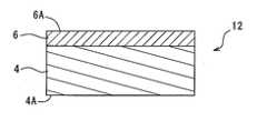
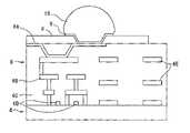
図1Aから図1Lは、本発明の第1実施形態に係る半導体チップ(素子チップ)2の製造工程を示している。最終工程図である図1Lと、半導体チップ2の詳細図である図2とを併せて参照すると、製造された半導体チップ2は、半導体層4と、半導体層4上に形成された配線層6と、配線層6上に形成された保護膜8および電極としてのバンプ10とを備える。なお、図2は断面図であるが、図示を明瞭にするため、ハッチングを省略している。バンプ10には一般に半田が使用され、半田はめっき法、印刷法、または蒸着法により形成される。半導体チップ2の保護膜8上にはUBM膜(アンダーバンプメタル膜)9が形成されており、バンプ10は、このUBM膜9上に形成されている。即ち、UBM膜9は、バンプ10の下地層であり、基本的には電気伝導性を有し、配線層6中のメタル配線6Bと電気的に接続されている。配線層6には、このようなメタル配線6Bと、絶縁膜6Cと、トランジスタ6Dとが設けられている。メタル配線6Bの材質は、例えばCu、Al、Al合金、またはW等であり得る。絶縁膜6Cの材質は、SiO2、SiN、SiOC、またはLow-k材料等であり得る。バンプ10に含まれる金属は、Cu、CuとSnとAgとの合金、AgとSnとの合金、Au、Al、またはAl合金等であり得る。バンプ10の形状は、特に限定されず、角柱、円柱、山型、ボール等であってもよい。バンプ10の配置および個数は特に限定されず、目的に応じて適宜設定される。ここで、電極としての凸型のバンプ10は、凹型のパッド電極であってもよい。また、配線層6には、TEG(Test Element Group)と呼ばれるメタル層6Eが設けられており、より詳細にはメタル層6Eは素子領域14(図1B参照)と分割領域16(図1B参照)とにわたって設けられている。(First Embodiment)
1A to 1L show a manufacturing process of a semiconductor chip (element chip) 2 according to the first embodiment of the present invention. With reference to FIG. 1L, which is a final process diagram, and FIG. 2, which is a detailed diagram of the
本実施形態では、バンプ10は、例えば、直径40μm、高さ50μmのCuピラー等である。また、配線層6は、例えば、Low-k材料とCu配線を備える厚み5μm程度の配線層である。また、半導体層4は、例えば、Siからなる厚み70μmの半導体層である。また、半導体層4の配線層6と反対側には、例えば、厚さ1μm程度のSiO2からなる絶縁膜層が設けられていてもよい。In the present embodiment, the
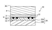
図1Aに示す第1準備工程では、半導体ウエハ(基板)12を準備する。図1Aに示すように、半導体ウエハ12は、半導体層4と、半導体層4上に形成された配線層6とを備える。 In the first preparation step shown in FIG. 1A, the semiconductor wafer (board) 12 is prepared. As shown in FIG. 1A, the
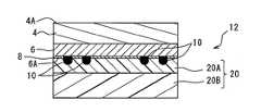
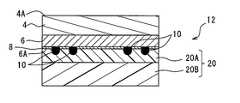
図1Bに示す第2準備工程では、半導体ウエハ12の配線層6の表面(第1の面)6Aに、保護膜8およびバンプ10を形成する。本工程を経た半導体ウエハ12は、バンプ10が形成された複数の素子領域14と、個々の素子領域14の周囲に隣接する分割領域16とを備える。換言すれば、分割領域16によって個々の素子領域14が画定されている。 In the second preparation step shown in FIG. 1B, the
図1Cに示す保護工程では、半導体ウエハ12の表面6Aに、裏面(第2の面)4Aの研削時の保護のためのBG(バックグラインド)テープ20を貼り付ける。BGテープ20は、粘着層20Aと、樹脂製の基材層20Bとからなるフィルムである。即ち、粘着層20Aを半導体ウエハ12の表面6Aに貼り付け、基材層20Bにより半導体ウエハ12の表面6Aを保護する。BGテープ20は、半導体ウエハ12に貼り付けられた後に、または、貼り付けられる前に、半導体ウエハ12の外形形状に合わせて切断されるため、半導体ウエハ12のハンドリング性は損なわれない。なお、BGテープ20は、保護テープの一例である。 In the protection step shown in FIG. 1C, a BG (back grind)
図1Dに示す薄化工程では、図示しない研削装置により半導体ウエハ12の裏面(第2の面)4A側から半導体層4を研削する。半導体ウエハ12は、半導体層4の研削により所定の厚みに薄化される。 In the thinning step shown in FIG. 1D, the
図1Eに示す第1保持工程では、ダイシングテープ(保持シート)22を半導体ウエハ12の裏面4Aに貼り付ける。本実施形態のダイシングテープ22は、アクリル系粘着剤からなる粘着層22Aと、樹脂製の基材層22Bとからなるフィルムである。粘着層22Aが半導体ウエハ12の裏面4Aに貼り付けられ、基材層22Bにより半導体ウエハ12が保持されている。また、ダイシングテープ22には、ハンドリング性の観点からフレーム22Cがその周囲に取り付けられている。 In the first holding step shown in FIG. 1E, the dicing tape (holding sheet) 22 is attached to the
図1Fに示す第2保持工程では、半導体ウエハ12からBGテープ20を剥離する。BGテープ20が剥離された状態では、半導体ウエハ12の表面6Aでバンプ10が露出している。 In the second holding step shown in FIG. 1F, the
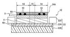
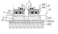
図1Gに示す第1マスク形成工程では、半導体ウエハ12の表面6Aに耐プラズマ性を有する下層マスク24Aを形成する。下層マスク24Aは、後述する個片化工程においてプラズマダイシングが行われる際に素子の表面がプラズマに晒されることを防ぐ。下層マスク24Aは、非水溶性の材質であって、後述する洗浄工程において水洗によって除去されない。例えば、本実施形態の下層マスク24Aの材質は、ポリオレフィンである。これに代えて、例えば、エチレンビニルアセテート共重合体であってもよい。本実施形態では、このような下層マスク24Aの形成は、原料液をスピンコート法によって半導体ウエハ12の表面6Aに塗布することで行われる。ただし、下層マスク24Aの形成方法は、スピンコート法に限らず、原料液を霧状に半導体ウエハ12の表面6Aにスプレーするスプレーコート法であってもよい。 In the first mask forming step shown in FIG. 1G, a
図1Hに示す第2マスク形成工程では、下層マスク24Aの上面に上層マスク24Bを形成する。上層マスク24Bは、後述するパターニング工程におけるレーザグルービングに伴って発生する加工屑(デブリ)が素子の表面に直接付着することを防ぐ。上層マスク24Bは、水溶性の材質であって、後述する洗浄工程において水洗によって除去される。例えば、本実施形態の上層マスク24Bの材質は、ポリビニルアルコールである。これに代えて、例えば、水溶性ポリエステルであってもよい。本実施形態では、このような下層マスク24Aの形成は、原料液をスピンコート法によって下層マスク24Aの上面に塗布することで行われる。ただし、下層マスク24Aの形成方法は、スピンコート法に限らず、原料液を霧状に下層マスク24Aの上面にスプレーするスプレーコート法であってもよい。また、以降、下層マスク24Aと上層マスク24Bとを合わせて単にマスク24ともいう。 In the second mask forming step shown in FIG. 1H, the
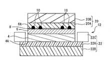
図1Iに示すパターニング工程では、分割領域16(図1H参照)に対応する部分において、マスク24と半導体ウエハ12とをレーザグルービングにより切削し、露出部18を形成する。詳細には、露出部18は、配線層6、保護膜8、およびマスク24を切削することで形成される。このとき、半導体層4は、一部切削されてもよいし切削されなくてもよいが、裏面4Aまでは切削されない。なお、配線層6中には、絶縁膜6Cおよびメタル層(TEG)6Eなどの金属層が設けられているが、これらもレーザで取り除き、露出部18を形成する。 In the patterning step shown in FIG. 1I, the
具体的には、レーザグルービングによる加工は以下のような条件にて行うことができる。レーザ光源には、UV波長(例えば355nm)のナノ秒レーザを用いる。そして、パルス周期40kHz、出力0.3W、およびスキャン速度200mm/秒で、分割領域16(図1H参照)へのレーザ光の照射を2回実施し、マスク24を除去する。その後、パルス周期25kHz、出力1.7W、およびスキャン速度100mm/秒で、分割領域16へのレーザ光の照射を1回実施し、保護膜8および配線層6を除去する。マスク24の除去のためのレーザ照射を、低出力条件で2回実施することで、マスク24の半導体ウエハ12からの剥がれ(デラミネーション)を抑制できる。また、配線層6を除去するためのレーザ照射を高出力条件で行うことで、配線層6がCuからなるメタル層(TEG)6Eを含む場合でも、配線層6を除去できる。 Specifically, the processing by laser grooving can be performed under the following conditions. As the laser light source, a nanosecond laser having a UV wavelength (for example, 355 nm) is used. Then, the divided region 16 (see FIG. 1H) is irradiated with the laser beam twice at a pulse period of 40 kHz, an output of 0.3 W, and a scan speed of 200 mm / sec, and the
図1Iに示すように、レーザグルービングでメタル層(TEG)6Eおよび絶縁膜6C(PI,PBO,SiN,SiO2,low-k等)等を加工すると、加工屑(デブリ)Dが発生する場合があり、デブリDにはこのTEGメタルやSiやSiOx等が含まれる。従って、露出部18には、溶融したデブリDが付着し、又、飛散したデブリDが上層マスク24Bの表面に付着することがある。特に、TEGメタルが多い箇所とその近傍にはデブリDが多く付着する傾向にある。レーザグルービングで上層マスク24Bの表面に付着したデブリDが除去されずにそのまま残留すると、後のプラズマダイシング工程において悪影響を及ぼし、いわゆるマイクロマスクの原因となる。As shown in FIG. 1I, when the metal layer (TEG) 6E and the insulating film 6C (PI, PBO, SiN, SiO2 , low-k, etc.) and the like are processed by laser grooving, processing debris D is generated. The debris D contains this TEG metal, Si, SiOx, and the like. Therefore, the molten debris D may adhere to the exposed
図1Jに示す洗浄工程では、水洗によって上層マスク24BとともにデブリDを除去する。前述のように、下層マスク24Aおよび上層マスク24Bの2層構造を採用しており、下層マスク24Aは水に溶解しないため、水洗後に下層マスク24Aを後のプラズマエッチングに対するマスクとして残すことができる。このようにしてデブリDを取り除くことで、後述するようにプラズマダイシング工程における半導体チップ2の表面の荒れを抑制できる。好ましくは、上記水洗は、温水であり、さらに好ましくは、残渣除去効率を上げるため、窒素をバブリングしながら行われる。なお、水に代えて水溶液を使用してもよい。 In the washing step shown in FIG. 1J, the debris D is removed together with the
同じく図1Jに示す乾燥工程では、上記洗浄工程の後に、窒素等によるブロー乾燥が行われる。これに代えて、半導体ウエハ12を載置した載置台(図示せず)をスピンさせることで、遠心力によって水などの洗浄液を振り落とすスピン乾燥が行われてもよい。 Similarly, in the drying step shown in FIG. 1J, blow drying with nitrogen or the like is performed after the above washing step. Instead of this, by spinning a mounting table (not shown) on which the
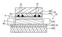
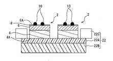
図1Kに示す個片化(プラズマダイシング)工程では、半導体ウエハ12の裏面4Aをダイシングテープ22で保持した状態で、半導体ウエハ12をプラズマエッチング(プラズマダイシング)により個片化する。 In the individualization (plasma dicing) step shown in FIG. 1K, the
図3は、本工程で使用されるドライエッチング装置50の一例を示している。ドライエッチング装置50のチャンバ52の頂部には誘電体窓(図示せず)が設けられており、誘電体窓の上方には上部電極としてのアンテナ54が配置されている。アンテナ54は、第1高周波電源部56に電気的に接続されている。一方、チャンバ52内の処理室58の底部側には、半導体ウエハ12が配置されるステージ60が配置されている。ステージ60には内部に冷媒流路(図示せず)が形成されており、冷媒流路に冷媒を循環させることにより、ステージ60は冷却される。ステージ60は下部電極としても機能し、第2高周波電源部62に電気的に接続されている。また、ステージ60は図示しない静電吸着用電極(ESC電極)を備え、ステージ60に載置されたダイシングテープ22(即ち半導体ウエハ12)をステージ60に静電吸着できるようになっている。また、ステージ60には冷却用ガスを供給するための図示しない冷却用ガス孔が設けられており、冷却用ガス孔からヘリウムなどの冷却用ガスを供給することで、ステージ60に静電吸着された半導体ウエハ12を冷却できる。チャンバ52のガス導入口64はエッチングガス源66に流体的に接続されており、排気口68はチャンバ52内を真空排気するための真空ポンプを含む真空排気部70に接続されている。 FIG. 3 shows an example of the
この個片化工程では、ダイシングテープ22を介して半導体ウエハ12をステージ60に載置し、処理室58内を真空排気部70によって真空排気するとともにエッチングガス源66から処理室58内に例えばSF6であるエッチングガスを供給する。そして、処理室58内を所定圧力に維持し、アンテナ54に対して第1高周波電源部56から高周波電力を供給し、処理室58内に第1のプラズマを発生させて半導体ウエハ12に照射する。このとき、第1のプラズマ中のラジカルとイオンの物理化学的作用により露出部18で露出している半導体ウエハ12の半導体層4が除去される。この個片化工程を経て、半導体ウエハ12は、個々の半導体チップ2に形成される。In this disintegration step, the
より詳細には、個片化工程は、(1)チャッキング工程、(2)クリーニング工程、(3)表面酸化物除去工程、(4)プラズマダイシング工程、および、(5)SiO2エッチング工程を含むことができる。More specifically, the individualization step includes (1) chucking step, (2) cleaning step, (3) surface oxide removing step, (4) plasma dicing step, and (5) SiO2 etching step. Can include.
(1)チャッキング工程
チャッキング工程では、チャンバ52内に高エネルギーのプラズマを発生させる前に、低エネルギーのプラズマを発生させて、ステージ60に載置された半導体ウエハ12およびダイシングテープ22を、ステージ60に確実に静電吸着させる。これにより、耐熱性に乏しいダイシングテープ22が、プラズマ処理に伴う熱ダメージを受け難くなる。例えば、弱いプラズマは、Arガスを100sccmで供給しながらチャンバ圧力を8Paに調圧し、アンテナ54に150WのRF電力を印加し、10秒程度発生させてもよい。このとき、ステージ60の温度を20℃以下に温度調節しながら、ESC電極に3kVの直流電圧を印加するとともに、冷却用ガスとして50~200PaのHeをダイシングテープ22とステージ60との間に供給することにより、半導体ウエハ12およびダイシングテープ22を冷却することができる。(1) Chucking Step In the chucking step, the
(2)クリーニング工程
レーザグルービングで生じ洗浄工程で除去しきれずに残存したデブリ(例えば金属デブリなど)や、レーザグルービングによりSiが溶けて生じたアモルファスシリコン層やシリコン酸化物層と前述した下層マスク(例えば、ポリオレフィンやエチレンビニルアセテート共重合体)の溶融物の混ざった層を除去するために、プラズマによるクリーニング工程を行ってもよい。クリーニング工程で使用するプラズマは、シリコン及びシリコン酸化物層が除去できるガス種を用いることが好ましく、例えば、SF6とO2の混合ガスを200sccmで供給しながら、チャンバ圧力を5Paに調圧し、アンテナ54に1000~2000WのRF電力を印加して発生させたプラズマに、1~2分程度晒せばよい。このとき、ステージ60が備える下部電極に150W程度のLF電力を印加することで、クリーニン効果を高くすることができる。また、クリーニング工程で発生させるプラズマによる熱ダメージを低減するため、クリーニング工程では半導体ウエハ12およびダイシングテープ22は冷却されることが好ましい。例えば、ステージ60の温度を20℃以下に温度調節しながら、ESC電極に3kVの直流電圧を印加するとともに、冷却用ガスとして50~200PaのHeをダイシングテープ22とステージ60の間に供給することにより、半導体ウエハ12およびダイシングテープ22を冷却することができる。(2) Cleaning process Debris (for example, metal debris) generated by laser grooving and remaining unremoved in the cleaning process, amorphous silicon layer or silicon oxide layer generated by melting Si by laser grooving, and the above-mentioned lower layer mask ( For example, in order to remove the layer mixed with the melt of polyolefin or ethylene vinyl acetate copolymer), a cleaning step using plasma may be performed. For the plasma used in the cleaning step, it is preferable to use a gas type that can remove silicon and the silicon oxide layer. For example, the chamber pressure is adjusted to 5 Pa while supplying a mixed gas of SF6 and O2 at 200 sccm. The
(3)表面酸化物除去工程
上記クリーニング工程で酸素を含有するプラズマによりクリーニングが行われる場合、クリーニング後のシリコンの表面が酸化される場合がある。そのため、クリーニング工程で生じたシリコン表面の酸化膜層を除去するために表面酸化物除去工程を設けてもよい。表面酸化物除去工程で使用するプラズマは、シリコン酸化物層が除去できるガス種を用いることが好ましく、例えば、SF6を200sccmで供給しながら、チャンバ圧力を8Paに調圧し、アンテナ54に2000~5000WのRF電力を印加して発生させたプラズマに、2~10秒程度晒せばよい。このとき、ステージ60が備える下部電極に500W程度のLF電力を印加することで、表面酸化物除去効果を高くすることができる。また、表面酸化物除去工程で発生させるプラズマによる熱ダメージを低減するため、表面酸化物除去工程では半導体ウエハ12およびダイシングテープ22は冷却されることが好ましい。例えば、ステージ60の温度を20℃以下に温度調節しながら、ESC電極に3kVの直流電圧を印加するとともに、冷却用ガスとして50~200PaのHeをダイシングテープ22とステージ60の間に供給することにより、半導体ウエハ12およびダイシングテープ22を冷却することができる。(3) Surface oxide removing step When cleaning is performed by plasma containing oxygen in the above cleaning step, the surface of silicon after cleaning may be oxidized. Therefore, a surface oxide removing step may be provided in order to remove the oxide film layer on the silicon surface generated in the cleaning step. For the plasma used in the surface oxide removing step, it is preferable to use a gas type that can remove the silicon oxide layer. For example, while supplying SF6 at 200 sccm, the chamber pressure is adjusted to 8 Pa, and 2000 to 2000 to the
(4)プラズマダイシング工程
プラズマダイシング工程では、BOSCH法によりシリコンからなる半導体層4を除去する。BOSCH法では、保護膜を堆積させるプラズマと、シリコンをエッチングするプラズマを交互に発生させる。保護膜を堆積させるプラズマは、例えば、C4F8を300sccmで供給しながら、チャンバ圧力を20Paに調圧し、アンテナ54に2000~5000WのRF電力を印加して、2~10秒程度発生させればよい。また、シリコンをエッチングするプラズマは、例えば、SF6を600sccmで供給しながら、チャンバ圧力を20Paに調圧し、アンテナ54に2000~5000WのRF電力を印加するとともに、下部電極に50~500WのLF電力を印加して、5~20秒程度発生させればよい。なお、半導体層4の加工形状におけるノッチングを抑制する為に、下部電極に印加する電力をパルス状にしてもよい。このような、保護膜を堆積させるプラズマの発生と、シリコンをエッチングするプラズマの発生とを、例えば、20サイクル程度繰り返すことで、半導体層4を除去することができる。なお、プラズマダイシング工程で発生させるプラズマによる熱ダメージを低減するため、プラズマダイシング工程では半導体ウエハ12およびダイシングテープ22は冷却されることが好ましい。例えば、ステージ60の温度を20℃以下に温度調節しながら、ESC電極に3kVの直流電圧を印加するとともに、冷却用ガスとして50~200PaのHeをダイシングテープ22とステージ60の間に供給することにより、半導体ウエハ12およびダイシングテープ22を冷却することができる。なお、半導体層4が所定以下の厚みである場合には、BOSCH法を使用せずに、シリコンを連続的にエッチングしてもよい。(4) Plasma dicing step In the plasma dicing step, the
(5)SiO2エッチング工程
半導体ウエハ12が半導体層4の下層にSiO2やDAF(ダイアタッチフィルム)を備える場合、プラズマダイシング工程の後で、エッチング条件を切り替えてこれらSiO2やDAFを加工してもよい。SiO2エッチング工程で使用するプラズマは、シリコン酸化物層が除去できるガス種を用いることが好ましく、例えば、ArとC4F8の混合ガスを300sccmで供給しながら、チャンバ圧力を1Paに調圧し、アンテナ54に500~2000WのRF電力を印加して発生させたプラズマに、2~8分程度晒せばよい。このとき、ステージ60が備える下部電極に500~1500W程度のLF電力を印加することで、SiO2エッチング効果を高くすることができる。また、SiO2エッチング工程で発生させるプラズマによる熱ダメージを低減するため、SiO2エッチング工程では半導体ウエハ12およびダイシングテープ22は冷却されることが好ましい。例えば、ステージ60の温度を20℃以下に温度調節しながら、ESC電極に3kVの直流電圧を印加するとともに、冷却用ガスとして50~200PaのHeをダイシングテープ22とステージ60の間に供給することにより、半導体ウエハ12およびダイシングテープ22を冷却することができる。(5) SiO2 Etching Step When the
図1Kに示すアッシング工程では、図3に示す処理室58内を真空排気部70によって真空排気するとともにエッチングガス源66から処理室58内に例えば酸素を含むエッチングガスを供給する。そして、処理室58内を所定圧力に維持し、アンテナ54に対して第1高周波電源部56から高周波電力を供給し、処理室58内に第2のプラズマを発生させて半導体ウエハ12に照射し、即ち下層マスク24Aの表面を第2のプラズマに晒す。このとき、第2のプラズマ中のラジカルとイオンの物理化学的作用により下層マスク24Aが除去される。 In the ashing step shown in FIG. 1K, the inside of the
アッシング工程にて、下層マスク24Aの残膜やデブリを除去するためには、酸素などのアッシングガスにCF4などの反応性のガスを加えて、SiやSiOxやマスク硬化層の除去効果を高めることが好ましい。また、メタル成分を除去するためには、Biasパワーを高くしてイオン性(スパッタ性)を高めた条件でプラズマエッチングを行うことが好ましい。アッシング工程で使用するプラズマは、下層マスク24の最表層の硬化層および変質層を除去できるガス種を用いることが好ましく、例えば、O2とCF4の混合ガスをできる。本工程では、例えばO2とCF4の混合ガスを300sccmで供給しながら、チャンバ圧力を1Paに調圧し、アンテナ54に2000~5000WのRF電力を印加して発生させたプラズマに、1~3分程度晒す。このとき、ステージ60が備える下部電極に100W程度のLF電力を印加することで、アッシング効果を高くすることができる。また、アッシング工程で発生させるプラズマによる熱ダメージを低減するため、表面酸化物除去工程では半導体ウエハ12およびダイシングテープ22は冷却されることが好ましい。例えば、ステージ60の温度を20℃以下に温度調節しながら、ESC電極に3kVの直流電圧を印加するとともに、冷却用ガスとして50~200PaのHeをダイシングテープ22とステージ60の間に供給することにより、半導体ウエハ12およびダイシングテープ22を冷却することができる。In order to remove the residual film and debris of the
上記アッシング工程後、半導体ウエハ12およびダイシングテープ22とステージ60との間の静電吸着力を低減させるデチャッキング工程を設けてもよい。デチャッキング工程では、チャンバ52内に弱いプラズマを発生させ、ステージ60に静電吸着されている半導体ウエハ12およびダイシングテープ22から、残留電荷を除去し、ステージ60との間の静電吸着力を低減させる。例えば、弱いプラズマは、Arガスを100sccmで供給しながらチャンバ圧力を12Paに調圧し、アンテナ54に150WのRF電力を印加し、30~120秒程度発生させてもよい。このとき、ステージ60の温度を20℃以下に温度調節しながら、ESC電極への電圧の印加と冷却用ガスの供給を停止して、弱いプラズマを発生させることが好ましい。 After the ashing step, a dechucking step may be provided to reduce the electrostatic adsorption force between the
上記の各工程を経て、製品として品質の高い半導体チップ2が製造される(図1L参照)。 Through each of the above steps, a high
図4は、半導体チップ2の製造方法を実行するクラスタ装置100の概略構成図である。クラスタ装置100の中央には、搬送機構180が設けられており、搬送機構180の周囲には前述の各工程に対応するクラスタ110~170が設けられている。ただし、図4に示す搬送機構180およびクラスタ110~170の配置や形状は、概念的なものであり、実際の配置や形状とは必ずしも一致しない。 FIG. 4 is a schematic configuration diagram of a
搬送機構180は、半導体ウエハ12ないしこれを個片化した半導体チップ2を各クラスタ110~170に搬送するものである。 The
クラスタ110は、半導体ウエハ12ないしこれを個片化した半導体チップ2を搬入出するためのものである。ここで、搬入される半導体ウエハ12は、第1準備工程から第2保持工程を既に完了した状態(図1F参照)である。また、搬出される半導体チップ2は、上記全工程を完了した状態(図1L参照)である。 The
クラスタ120は、第1マスク形成工程(図1G参照)が実行されるクラスタである。クラスタ130は、第2マスク形成工程(図1H参照)が実行されるクラスタである。クラスタ140は、パターニング工程(図1I参照)が実行されるクラスタである。クラスタ150は、洗浄工程(図1J参照)が実行されるクラスタである。クラスタ160は、乾燥工程(同じく図1J参照)が実行されるクラスタである。クラスタ170は、個片化工程(図1K参照)およびアッシング工程(図1L参照)が実行されるクラスタである。これらのクラスタ110~170の分類は、概念的なものであり、必ずしも上記のものに限定さない。例えば、第1マスク形成工程を実行するクラスタ120および第2マスク形成工程を実行するクラスタ130は同じクラスタであってもよい。また、水洗工程を実行するクラスタ150および乾燥工程を実行するクラスタ160は同じクラスタであってもよい。 The
本実施形態によれば、パターニング工程におけるレーザグルービング加工の前に半導体ウエハ12の表面6Aに水溶性の上層マスク24Bを形成しているため、その後のレーザグルービング加工で上層マスク24Bに付着したデブリを、上層マスク24Bとともに水洗により除去できる。従って、プラズマダイシングにおけるデブリの残留を抑制できるため、プラズマダイシングにおいてデブリに起因する加工不良を抑制でき、製品としての半導体チップ2の信頼性を向上できる。 According to the present embodiment, since the water-soluble
また、本実施形態によれば、アッシング工程において、第2のプラズマによるアッシングによって、非水溶性の下層マスク24Aを容易に除去できる。 Further, according to the present embodiment, in the ashing step, the water-insoluble
また、本実施形態によれば、第1マスク形成工程および第2マスク形成工程において、上層マスク24Bおよび下層マスク24Aを原料液の塗布によって形成できるため、上層マスク24Bおよび下層マスク24Aを容易に形成できる。 Further, according to the present embodiment, since the
(第2実施形態)
図5A~5Lに示す本実施形態の半導体チップ2の製造方法は、下層マスク24の形成方法が第1実施形態とは異なる。これに関する以外は、第1実施形態の半導体チップ2の製造方法と実質的に同じである。従って、第1実施形態にて説明した部分については説明を省略する場合がある。(Second Embodiment)
In the method for manufacturing the
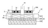
図5Aに示す第1準備工程、図5Bに示す第2準備工程、図5Cに示す保護工程、図5Dに示す薄化工程、および図5Eに示す第1保持工程は、第1実施形態と実質的に同じである。ただし、本実施形態で用いられるBGテープ20は、基材20Bと非水溶性の粘着層20Aとからなり、粘着層20Aを残して基材20Bを剥離できるようになっている。特に、粘着層20Aは、耐プラズマ性を有しており、個片化工程(図5J参照)においてプラズマから素子領域14を保護することができる。 The first preparation step shown in FIG. 5A, the second preparation step shown in FIG. 5B, the protection step shown in FIG. 5C, the thinning step shown in FIG. 5D, and the first holding step shown in FIG. Is the same. However, the
図5Fに示す第1マスク形成工程では、BGテープ20のうち、基材20Bのみを剥離する。即ち、粘着層20Aを残存させて、第1実施形態の下層マスク24A(図1G参照)として利用する。 In the first mask forming step shown in FIG. 5F, only the
図5Gに示す第2マスク形成工程では、粘着層20Aの上面に上層マスク24Bを形成する。上層マスク24Bは、第1実施形態と同じものあり、その形成方法も第1実施形態と同じである。 In the second mask forming step shown in FIG. 5G, the
図5Hに示すパターニング工程、図5Iに示す洗浄工程、図5Jに示す個片化工程、および図5Kに示すアッシング工程は、第1実施形態の下層マスク24Aが粘着層20Aに置換された点以外、第1実施形態と実質的に同じである。 The patterning step shown in FIG. 5H, the cleaning step shown in FIG. 5I, the individualization step shown in FIG. 5J, and the ashing step shown in FIG. , It is substantially the same as the first embodiment.
上記の各工程を経て、製品として品質の高い半導体チップ2が製造される(図5L参照)。 Through each of the above steps, a high
本実施形態によれば、BGテープ20の粘着層20Aを第1実施形態の下層マスク24Aとして利用できるため、マスク形成の工程を簡略化できる。 According to the present embodiment, since the
以上より、本発明の具体的な実施形態およびその変形例について説明したが、本発明は上記形態に限定されるものではなく、この発明の範囲内で種々変更して実施することができる。例えば、個々の実施形態の内容を適宜組み合わせたものを、この発明の一実施形態としてもよい。 Although the specific embodiment of the present invention and the modification thereof have been described above, the present invention is not limited to the above-described embodiment and can be variously modified and carried out within the scope of the present invention. For example, an embodiment of the present invention may be a combination of the contents of the individual embodiments as appropriate.
2 半導体チップ(素子チップ)
4 半導体層
4A 裏面(第2の面)
6 配線層
6A 表面(第1の面)
6B メタル配線
6C 絶縁膜
6D トランジスタ
6E メタル層(TEG)
8 保護膜
9 UBM膜
10 バンプ
12 半導体ウエハ(基板)
14 素子領域
16 分割領域
18 露出部
20 BGテープ
20A 粘着層
20B 基材層
22 ダイシングテープ(保持シート)
22A 粘着層
22B 基材層
22C フレーム
24 マスク
24A 下層マスク(下層)
24B 上層マスク(上層)
50 ドライエッチング装置
52 チャンバ
54 アンテナ
56 第1高周波電源部
58 処理室
60 ステージ
62 第2高周波電源部
64 ガス導入口
66 エッチングガス源
68 排気口
70 真空排気部
100 クラスタ装置
110,120,130,140,150,160,170 クラスタ
180 搬送機構2 Semiconductor chip (element chip)
6
6B metal wiring
8 Protective film 9
14
24B upper layer mask (upper layer)
50
Claims (3)
Translated fromJapanese基材と非水溶性の粘着層とを備える保護テープを、前記粘着層を介して前記第1の面に貼り付け、
前記基板の前記第2の面の側から前記基板を研削することにより前記基板を薄化し、
前記基板の前記第2の面を保持シートに保持し、
前記基板の前記第1の面を、非水溶性の下層と水溶性の上層とを備えるマスクで被覆し、
前記マスクにレーザ光を照射することにより前記マスクに開口を形成して前記基板の分割領域を露出させ、
前記基板を水または水溶液と接触させて、前記素子領域を覆う前記マスクの前記上層を除去しつつ前記下層を残存させ、
前記基板を第1のプラズマに晒して、前記開口に露出する前記分割領域を前記第2の面に達するまでエッチングすることで複数の素子チップに個片化し、前記複数の素子チップが前記保持シートに保持された状態とし、
前記複数の素子チップの表面に残存する前記マスクを除去し、前記マスクの除去された前記複数の素子チップが前記保持シートに保持された状態とする
ことを含み、
前記マスクによる被覆は、前記保護テープの前記基材を前記基板から剥がして前記粘着層を前記基板の前記第1の面に残存させて前記下層とし、前記下層の上に前記上層を形成することを含む、
素子チップの製造方法。A substrate having a plurality of element regions and a divided region defining the element regions, and having a first surface and a second surface opposite to the first surface is prepared.
A protective tape comprising a base material and a water-insoluble adhesive layer is attached to the first surface via the adhesive layer.
The substrate is thinned by grinding the substrate from the side of the second surface of the substrate.
The second surface of the substrate is held on the holding sheet, and the second surface is held on the holding sheet.
The first surface of the substrate is covered with a mask comprising a water-insoluble lower layer and a water-soluble upper layer.
By irradiating the mask with a laser beam, an opening is formed in the mask to expose the divided region of the substrate.
The substrate is brought into contact with water or an aqueous solution to remove the upper layer of the mask covering the element region while leaving the lower layer.
The substrate is exposed to the first plasma, and the divided region exposed to the opening is etched until it reaches the second surface to be separated into a plurality of element chips, and the plurality of element chips are formed into the holding sheet. In the state of being held in
This includes removing the mask remaining on the surface of the plurality of element chips so that the plurality of element chips from which the mask has been removed are held by the holding sheet.
In the coating with the mask, the base material of the protective tape is peeled off from the substrate, the adhesive layer is left on the first surface of the substrate to form the lower layer, and the upper layer is formed on the lower layer. including,
Manufacturing method of element chip.
Priority Applications (3)
| Application Number | Priority Date | Filing Date | Title |
|---|---|---|---|
| JP2017172366AJP7042437B2 (en) | 2017-09-07 | 2017-09-07 | Method of manufacturing element chips |
| US16/103,025US10607846B2 (en) | 2017-09-07 | 2018-08-14 | Method of manufacturing element chip |
| CN201811029474.3ACN109473352B (en) | 2017-09-07 | 2018-09-04 | Manufacturing method of component chip |
Applications Claiming Priority (1)
| Application Number | Priority Date | Filing Date | Title |
|---|---|---|---|
| JP2017172366AJP7042437B2 (en) | 2017-09-07 | 2017-09-07 | Method of manufacturing element chips |
Publications (2)
| Publication Number | Publication Date |
|---|---|
| JP2019050237A JP2019050237A (en) | 2019-03-28 |
| JP7042437B2true JP7042437B2 (en) | 2022-03-28 |
Family
ID=65518294
Family Applications (1)
| Application Number | Title | Priority Date | Filing Date |
|---|---|---|---|
| JP2017172366AActiveJP7042437B2 (en) | 2017-09-07 | 2017-09-07 | Method of manufacturing element chips |
Country Status (3)
| Country | Link |
|---|---|
| US (1) | US10607846B2 (en) |
| JP (1) | JP7042437B2 (en) |
| CN (1) | CN109473352B (en) |
Families Citing this family (2)
| Publication number | Priority date | Publication date | Assignee | Title |
|---|---|---|---|---|
| JP7570030B2 (en)* | 2020-12-04 | 2024-10-21 | パナソニックIpマネジメント株式会社 | Manufacturing method of element chip |
| CN114446876B (en)* | 2022-04-12 | 2022-07-01 | 湖北三维半导体集成创新中心有限责任公司 | Wafer cutting method |
Citations (6)
| Publication number | Priority date | Publication date | Assignee | Title |
|---|---|---|---|---|
| JP2008053417A (en) | 2006-08-24 | 2008-03-06 | Matsushita Electric Ind Co Ltd | Semiconductor chip manufacturing method and semiconductor wafer processing method |
| JP2014523112A (en) | 2011-06-15 | 2014-09-08 | アプライド マテリアルズ インコーポレイテッド | Water-soluble mask for substrate dicing by laser plasma etching |
| JP2014523110A (en) | 2011-06-15 | 2014-09-08 | アプライド マテリアルズ インコーポレイテッド | In-situ deposition mask layer for device singulation by laser scribing and plasma etching |
| JP2014523109A (en) | 2011-06-15 | 2014-09-08 | アプライド マテリアルズ インコーポレイテッド | Multilayer mask for laser substrate dicing and plasma etching |
| WO2017082210A1 (en) | 2015-11-09 | 2017-05-18 | 古河電気工業株式会社 | Method for manufacturing semiconductor chip, and mask-integrated surface protection tape used therein |
| JP2018041935A (en) | 2016-09-09 | 2018-03-15 | 株式会社ディスコ | Split method |
Family Cites Families (18)
| Publication number | Priority date | Publication date | Assignee | Title |
|---|---|---|---|---|
| US9126285B2 (en)* | 2011-06-15 | 2015-09-08 | Applied Materials, Inc. | Laser and plasma etch wafer dicing using physically-removable mask |
| JP2014029921A (en)* | 2012-07-31 | 2014-02-13 | Sony Corp | Semiconductor device processing method and semiconductor substrate processed article |
| JP6062254B2 (en)* | 2013-01-15 | 2017-01-18 | 株式会社ディスコ | Wafer processing method |
| US8980726B2 (en)* | 2013-01-25 | 2015-03-17 | Applied Materials, Inc. | Substrate dicing by laser ablation and plasma etch damage removal for ultra-thin wafers |
| TWI619165B (en)* | 2013-03-14 | 2018-03-21 | 應用材料股份有限公司 | Multi-layer mask with non-light definable laser energy absorbing layer for substrate cutting by laser and plasma etching |
| US20150011073A1 (en)* | 2013-07-02 | 2015-01-08 | Wei-Sheng Lei | Laser scribing and plasma etch for high die break strength and smooth sidewall |
| US20150255349A1 (en)* | 2014-03-07 | 2015-09-10 | JAMES Matthew HOLDEN | Approaches for cleaning a wafer during hybrid laser scribing and plasma etching wafer dicing processes |
| JP6347657B2 (en)* | 2014-04-22 | 2018-06-27 | デクセリアルズ株式会社 | Protective tape and method of manufacturing semiconductor device using the same |
| US8980727B1 (en)* | 2014-05-07 | 2015-03-17 | Applied Materials, Inc. | Substrate patterning using hybrid laser scribing and plasma etching processing schemes |
| JP6738591B2 (en) | 2015-03-13 | 2020-08-12 | 古河電気工業株式会社 | Semiconductor wafer processing method, semiconductor chip, and surface protection tape |
| JP6454580B2 (en)* | 2015-03-30 | 2019-01-16 | デクセリアルズ株式会社 | Thermosetting adhesive sheet and method for manufacturing semiconductor device |
| JP6517588B2 (en)* | 2015-05-27 | 2019-05-22 | デクセリアルズ株式会社 | Thermosetting adhesive sheet and method of manufacturing semiconductor device |
| JP6599134B2 (en)* | 2015-06-04 | 2019-10-30 | デクセリアルズ株式会社 | Protective tape and method of manufacturing semiconductor device using the same |
| JP6595296B2 (en)* | 2015-10-19 | 2019-10-23 | デクセリアルズ株式会社 | Protective tape and method for manufacturing semiconductor device |
| JP7165976B2 (en)* | 2016-03-30 | 2022-11-07 | ナノブリッジ・セミコンダクター株式会社 | Variable resistance element and method for manufacturing variable resistance element |
| US11158540B2 (en)* | 2017-05-26 | 2021-10-26 | Applied Materials, Inc. | Light-absorbing mask for hybrid laser scribing and plasma etch wafer singulation process |
| US10363629B2 (en)* | 2017-06-01 | 2019-07-30 | Applied Materials, Inc. | Mitigation of particle contamination for wafer dicing processes |
| JP6994646B2 (en)* | 2018-01-17 | 2022-01-14 | パナソニックIpマネジメント株式会社 | Method of manufacturing element chips |
- 2017
- 2017-09-07JPJP2017172366Apatent/JP7042437B2/enactiveActive
- 2018
- 2018-08-14USUS16/103,025patent/US10607846B2/enactiveActive
- 2018-09-04CNCN201811029474.3Apatent/CN109473352B/enactiveActive
Patent Citations (6)
| Publication number | Priority date | Publication date | Assignee | Title |
|---|---|---|---|---|
| JP2008053417A (en) | 2006-08-24 | 2008-03-06 | Matsushita Electric Ind Co Ltd | Semiconductor chip manufacturing method and semiconductor wafer processing method |
| JP2014523112A (en) | 2011-06-15 | 2014-09-08 | アプライド マテリアルズ インコーポレイテッド | Water-soluble mask for substrate dicing by laser plasma etching |
| JP2014523110A (en) | 2011-06-15 | 2014-09-08 | アプライド マテリアルズ インコーポレイテッド | In-situ deposition mask layer for device singulation by laser scribing and plasma etching |
| JP2014523109A (en) | 2011-06-15 | 2014-09-08 | アプライド マテリアルズ インコーポレイテッド | Multilayer mask for laser substrate dicing and plasma etching |
| WO2017082210A1 (en) | 2015-11-09 | 2017-05-18 | 古河電気工業株式会社 | Method for manufacturing semiconductor chip, and mask-integrated surface protection tape used therein |
| JP2018041935A (en) | 2016-09-09 | 2018-03-15 | 株式会社ディスコ | Split method |
Also Published As
| Publication number | Publication date |
|---|---|
| US20190074185A1 (en) | 2019-03-07 |
| CN109473352B (en) | 2023-08-01 |
| JP2019050237A (en) | 2019-03-28 |
| CN109473352A (en) | 2019-03-15 |
| US10607846B2 (en) | 2020-03-31 |
Similar Documents
| Publication | Publication Date | Title |
|---|---|---|
| US10923362B2 (en) | Manufacturing process of element chip | |
| JP6519759B2 (en) | Method of manufacturing element chip | |
| JP6770858B2 (en) | Dividing method | |
| US7989266B2 (en) | Methods for separating individual semiconductor devices from a carrier | |
| JP6524594B2 (en) | Method of manufacturing element chip | |
| CN105514038B (en) | Method for cutting semiconductor wafer | |
| US20160307851A1 (en) | Method of dividing wafer | |
| CN111312658B (en) | Wafer processing method | |
| US10276423B2 (en) | Method of manufacturing element chip | |
| JP7042437B2 (en) | Method of manufacturing element chips | |
| US11024542B2 (en) | Manufacturing method of device chip | |
| TW201936476A (en) | Peeling method for peeling off substrate from support plate | |
| JP2019212769A (en) | Wafer processing method | |
| CN115424944A (en) | Method for manufacturing device chip | |
| JP2019169686A (en) | Manufacturing method of element chip | |
| JP7207969B2 (en) | Wafer processing method | |
| JP6689154B2 (en) | Device wafer processing method | |
| JP2021015938A (en) | Water-soluble resin sheet and wafer processing method | |
| JP2019212824A (en) | Wafer processing method | |
| JP2018018907A (en) | Device wafer processing method | |
| JP2020061500A (en) | Wafer processing method | |
| JP2019153799A (en) | Method for manufacturing device chips | |
| JP2019212771A (en) | Wafer processing method |
Legal Events
| Date | Code | Title | Description |
|---|---|---|---|
| A621 | Written request for application examination | Free format text:JAPANESE INTERMEDIATE CODE: A621 Effective date:20200713 | |
| A977 | Report on retrieval | Free format text:JAPANESE INTERMEDIATE CODE: A971007 Effective date:20210630 | |
| A131 | Notification of reasons for refusal | Free format text:JAPANESE INTERMEDIATE CODE: A131 Effective date:20210803 | |
| A521 | Request for written amendment filed | Free format text:JAPANESE INTERMEDIATE CODE: A523 Effective date:20210922 | |
| TRDD | Decision of grant or rejection written | ||
| A01 | Written decision to grant a patent or to grant a registration (utility model) | Free format text:JAPANESE INTERMEDIATE CODE: A01 Effective date:20220208 | |
| A61 | First payment of annual fees (during grant procedure) | Free format text:JAPANESE INTERMEDIATE CODE: A61 Effective date:20220225 | |
| R151 | Written notification of patent or utility model registration | Ref document number:7042437 Country of ref document:JP Free format text:JAPANESE INTERMEDIATE CODE: R151 |