JP7039908B2 - Semiconductor device - Google Patents
Semiconductor deviceDownload PDFInfo
- Publication number
- JP7039908B2 JP7039908B2JP2017185098AJP2017185098AJP7039908B2JP 7039908 B2JP7039908 B2JP 7039908B2JP 2017185098 AJP2017185098 AJP 2017185098AJP 2017185098 AJP2017185098 AJP 2017185098AJP 7039908 B2JP7039908 B2JP 7039908B2
- Authority
- JP
- Japan
- Prior art keywords
- cooling plate
- cooler
- package
- resin
- semiconductor
- Prior art date
- Legal status (The legal status is an assumption and is not a legal conclusion. Google has not performed a legal analysis and makes no representation as to the accuracy of the status listed.)
- Active
Links
Images


Classifications
- H—ELECTRICITY
- H01—ELECTRIC ELEMENTS
- H01L—SEMICONDUCTOR DEVICES NOT COVERED BY CLASS H10
- H01L23/00—Details of semiconductor or other solid state devices
- H01L23/34—Arrangements for cooling, heating, ventilating or temperature compensation ; Temperature sensing arrangements
- H01L23/36—Selection of materials, or shaping, to facilitate cooling or heating, e.g. heatsinks
- H01L23/367—Cooling facilitated by shape of device
- H—ELECTRICITY
- H01—ELECTRIC ELEMENTS
- H01L—SEMICONDUCTOR DEVICES NOT COVERED BY CLASS H10
- H01L23/00—Details of semiconductor or other solid state devices
- H01L23/34—Arrangements for cooling, heating, ventilating or temperature compensation ; Temperature sensing arrangements
- H01L23/36—Selection of materials, or shaping, to facilitate cooling or heating, e.g. heatsinks
- H01L23/373—Cooling facilitated by selection of materials for the device or materials for thermal expansion adaptation, e.g. carbon
- H01L23/3737—Organic materials with or without a thermoconductive filler
- F—MECHANICAL ENGINEERING; LIGHTING; HEATING; WEAPONS; BLASTING
- F28—HEAT EXCHANGE IN GENERAL
- F28D—HEAT-EXCHANGE APPARATUS, NOT PROVIDED FOR IN ANOTHER SUBCLASS, IN WHICH THE HEAT-EXCHANGE MEDIA DO NOT COME INTO DIRECT CONTACT
- F28D1/00—Heat-exchange apparatus having stationary conduit assemblies for one heat-exchange medium only, the media being in contact with different sides of the conduit wall, in which the other heat-exchange medium is a large body of fluid, e.g. domestic or motor car radiators
- F28D1/02—Heat-exchange apparatus having stationary conduit assemblies for one heat-exchange medium only, the media being in contact with different sides of the conduit wall, in which the other heat-exchange medium is a large body of fluid, e.g. domestic or motor car radiators with heat-exchange conduits immersed in the body of fluid
- F28D1/03—Heat-exchange apparatus having stationary conduit assemblies for one heat-exchange medium only, the media being in contact with different sides of the conduit wall, in which the other heat-exchange medium is a large body of fluid, e.g. domestic or motor car radiators with heat-exchange conduits immersed in the body of fluid with plate-like or laminated conduits
- F28D1/0366—Heat-exchange apparatus having stationary conduit assemblies for one heat-exchange medium only, the media being in contact with different sides of the conduit wall, in which the other heat-exchange medium is a large body of fluid, e.g. domestic or motor car radiators with heat-exchange conduits immersed in the body of fluid with plate-like or laminated conduits the conduits being formed by spaced plates with inserted elements
- F—MECHANICAL ENGINEERING; LIGHTING; HEATING; WEAPONS; BLASTING
- F28—HEAT EXCHANGE IN GENERAL
- F28F—DETAILS OF HEAT-EXCHANGE AND HEAT-TRANSFER APPARATUS, OF GENERAL APPLICATION
- F28F3/00—Plate-like or laminated elements; Assemblies of plate-like or laminated elements
- F28F3/02—Elements or assemblies thereof with means for increasing heat-transfer area, e.g. with fins, with recesses, with corrugations
- H—ELECTRICITY
- H01—ELECTRIC ELEMENTS
- H01L—SEMICONDUCTOR DEVICES NOT COVERED BY CLASS H10
- H01L23/00—Details of semiconductor or other solid state devices
- H01L23/02—Containers; Seals
- H01L23/04—Containers; Seals characterised by the shape of the container or parts, e.g. caps, walls
- H01L23/043—Containers; Seals characterised by the shape of the container or parts, e.g. caps, walls the container being a hollow construction and having a conductive base as a mounting as well as a lead for the semiconductor body
- H01L23/051—Containers; Seals characterised by the shape of the container or parts, e.g. caps, walls the container being a hollow construction and having a conductive base as a mounting as well as a lead for the semiconductor body another lead being formed by a cover plate parallel to the base plate, e.g. sandwich type
- H—ELECTRICITY
- H01—ELECTRIC ELEMENTS
- H01L—SEMICONDUCTOR DEVICES NOT COVERED BY CLASS H10
- H01L23/00—Details of semiconductor or other solid state devices
- H01L23/28—Encapsulations, e.g. encapsulating layers, coatings, e.g. for protection
- H01L23/31—Encapsulations, e.g. encapsulating layers, coatings, e.g. for protection characterised by the arrangement or shape
- H01L23/3107—Encapsulations, e.g. encapsulating layers, coatings, e.g. for protection characterised by the arrangement or shape the device being completely enclosed
- H01L23/3121—Encapsulations, e.g. encapsulating layers, coatings, e.g. for protection characterised by the arrangement or shape the device being completely enclosed a substrate forming part of the encapsulation
- H—ELECTRICITY
- H01—ELECTRIC ELEMENTS
- H01L—SEMICONDUCTOR DEVICES NOT COVERED BY CLASS H10
- H01L23/00—Details of semiconductor or other solid state devices
- H01L23/34—Arrangements for cooling, heating, ventilating or temperature compensation ; Temperature sensing arrangements
- H01L23/36—Selection of materials, or shaping, to facilitate cooling or heating, e.g. heatsinks
- H01L23/367—Cooling facilitated by shape of device
- H01L23/3672—Foil-like cooling fins or heat sinks
- H—ELECTRICITY
- H01—ELECTRIC ELEMENTS
- H01L—SEMICONDUCTOR DEVICES NOT COVERED BY CLASS H10
- H01L23/00—Details of semiconductor or other solid state devices
- H01L23/34—Arrangements for cooling, heating, ventilating or temperature compensation ; Temperature sensing arrangements
- H01L23/44—Arrangements for cooling, heating, ventilating or temperature compensation ; Temperature sensing arrangements the complete device being wholly immersed in a fluid other than air
- H—ELECTRICITY
- H01—ELECTRIC ELEMENTS
- H01L—SEMICONDUCTOR DEVICES NOT COVERED BY CLASS H10
- H01L23/00—Details of semiconductor or other solid state devices
- H01L23/34—Arrangements for cooling, heating, ventilating or temperature compensation ; Temperature sensing arrangements
- H01L23/46—Arrangements for cooling, heating, ventilating or temperature compensation ; Temperature sensing arrangements involving the transfer of heat by flowing fluids
- H01L23/473—Arrangements for cooling, heating, ventilating or temperature compensation ; Temperature sensing arrangements involving the transfer of heat by flowing fluids by flowing liquids
- H—ELECTRICITY
- H01—ELECTRIC ELEMENTS
- H01L—SEMICONDUCTOR DEVICES NOT COVERED BY CLASS H10
- H01L25/00—Assemblies consisting of a plurality of semiconductor or other solid state devices
- H01L25/03—Assemblies consisting of a plurality of semiconductor or other solid state devices all the devices being of a type provided for in a single subclass of subclasses H10B, H10D, H10F, H10H, H10K or H10N, e.g. assemblies of rectifier diodes
- H01L25/04—Assemblies consisting of a plurality of semiconductor or other solid state devices all the devices being of a type provided for in a single subclass of subclasses H10B, H10D, H10F, H10H, H10K or H10N, e.g. assemblies of rectifier diodes the devices not having separate containers
- H01L25/07—Assemblies consisting of a plurality of semiconductor or other solid state devices all the devices being of a type provided for in a single subclass of subclasses H10B, H10D, H10F, H10H, H10K or H10N, e.g. assemblies of rectifier diodes the devices not having separate containers the devices being of a type provided for in group subclass H10D
- H01L25/071—Assemblies consisting of a plurality of semiconductor or other solid state devices all the devices being of a type provided for in a single subclass of subclasses H10B, H10D, H10F, H10H, H10K or H10N, e.g. assemblies of rectifier diodes the devices not having separate containers the devices being of a type provided for in group subclass H10D the devices being arranged next and on each other, i.e. mixed assemblies
- F—MECHANICAL ENGINEERING; LIGHTING; HEATING; WEAPONS; BLASTING
- F28—HEAT EXCHANGE IN GENERAL
- F28D—HEAT-EXCHANGE APPARATUS, NOT PROVIDED FOR IN ANOTHER SUBCLASS, IN WHICH THE HEAT-EXCHANGE MEDIA DO NOT COME INTO DIRECT CONTACT
- F28D21/00—Heat-exchange apparatus not covered by any of the groups F28D1/00 - F28D20/00
- F28D2021/0019—Other heat exchangers for particular applications; Heat exchange systems not otherwise provided for
- F28D2021/0028—Other heat exchangers for particular applications; Heat exchange systems not otherwise provided for for cooling heat generating elements, e.g. for cooling electronic components or electric devices
- F28D2021/0029—Heat sinks
- F—MECHANICAL ENGINEERING; LIGHTING; HEATING; WEAPONS; BLASTING
- F28—HEAT EXCHANGE IN GENERAL
- F28F—DETAILS OF HEAT-EXCHANGE AND HEAT-TRANSFER APPARATUS, OF GENERAL APPLICATION
- F28F21/00—Constructions of heat-exchange apparatus characterised by the selection of particular materials
- F28F21/06—Constructions of heat-exchange apparatus characterised by the selection of particular materials of plastics material
- F28F21/065—Constructions of heat-exchange apparatus characterised by the selection of particular materials of plastics material the heat-exchange apparatus employing plate-like or laminated conduits
- F—MECHANICAL ENGINEERING; LIGHTING; HEATING; WEAPONS; BLASTING
- F28—HEAT EXCHANGE IN GENERAL
- F28F—DETAILS OF HEAT-EXCHANGE AND HEAT-TRANSFER APPARATUS, OF GENERAL APPLICATION
- F28F2255/00—Heat exchanger elements made of materials having special features or resulting from particular manufacturing processes
- F28F2255/06—Heat exchanger elements made of materials having special features or resulting from particular manufacturing processes composite, e.g. polymers with fillers or fibres
- F—MECHANICAL ENGINEERING; LIGHTING; HEATING; WEAPONS; BLASTING
- F28—HEAT EXCHANGE IN GENERAL
- F28F—DETAILS OF HEAT-EXCHANGE AND HEAT-TRANSFER APPARATUS, OF GENERAL APPLICATION
- F28F3/00—Plate-like or laminated elements; Assemblies of plate-like or laminated elements
- F28F3/02—Elements or assemblies thereof with means for increasing heat-transfer area, e.g. with fins, with recesses, with corrugations
- F28F3/022—Elements or assemblies thereof with means for increasing heat-transfer area, e.g. with fins, with recesses, with corrugations the means being wires or pins
- H—ELECTRICITY
- H01—ELECTRIC ELEMENTS
- H01L—SEMICONDUCTOR DEVICES NOT COVERED BY CLASS H10
- H01L2224/00—Indexing scheme for arrangements for connecting or disconnecting semiconductor or solid-state bodies and methods related thereto as covered by H01L24/00
- H01L2224/01—Means for bonding being attached to, or being formed on, the surface to be connected, e.g. chip-to-package, die-attach, "first-level" interconnects; Manufacturing methods related thereto
- H01L2224/26—Layer connectors, e.g. plate connectors, solder or adhesive layers; Manufacturing methods related thereto
- H01L2224/31—Structure, shape, material or disposition of the layer connectors after the connecting process
- H01L2224/33—Structure, shape, material or disposition of the layer connectors after the connecting process of a plurality of layer connectors
- H01L2224/331—Disposition
- H01L2224/3318—Disposition being disposed on at least two different sides of the body, e.g. dual array
- H01L2224/33181—On opposite sides of the body
- H—ELECTRICITY
- H01—ELECTRIC ELEMENTS
- H01L—SEMICONDUCTOR DEVICES NOT COVERED BY CLASS H10
- H01L23/00—Details of semiconductor or other solid state devices
- H01L23/28—Encapsulations, e.g. encapsulating layers, coatings, e.g. for protection
- H01L23/31—Encapsulations, e.g. encapsulating layers, coatings, e.g. for protection characterised by the arrangement or shape
- H01L23/3107—Encapsulations, e.g. encapsulating layers, coatings, e.g. for protection characterised by the arrangement or shape the device being completely enclosed
- H—ELECTRICITY
- H01—ELECTRIC ELEMENTS
- H01L—SEMICONDUCTOR DEVICES NOT COVERED BY CLASS H10
- H01L23/00—Details of semiconductor or other solid state devices
- H01L23/34—Arrangements for cooling, heating, ventilating or temperature compensation ; Temperature sensing arrangements
- H01L23/36—Selection of materials, or shaping, to facilitate cooling or heating, e.g. heatsinks
- H01L23/373—Cooling facilitated by selection of materials for the device or materials for thermal expansion adaptation, e.g. carbon
- H—ELECTRICITY
- H01—ELECTRIC ELEMENTS
- H01L—SEMICONDUCTOR DEVICES NOT COVERED BY CLASS H10
- H01L2924/00—Indexing scheme for arrangements or methods for connecting or disconnecting semiconductor or solid-state bodies as covered by H01L24/00
- H01L2924/15—Details of package parts other than the semiconductor or other solid state devices to be connected
- H01L2924/181—Encapsulation
Landscapes
- Engineering & Computer Science (AREA)
- Physics & Mathematics (AREA)
- Microelectronics & Electronic Packaging (AREA)
- Power Engineering (AREA)
- Computer Hardware Design (AREA)
- General Physics & Mathematics (AREA)
- Condensed Matter Physics & Semiconductors (AREA)
- Chemical & Material Sciences (AREA)
- Materials Engineering (AREA)
- Thermal Sciences (AREA)
- Mechanical Engineering (AREA)
- General Engineering & Computer Science (AREA)
- Cooling Or The Like Of Semiconductors Or Solid State Devices (AREA)
Description
Translated fromJapanese本明細書が開示する技術は、半導体素子を封止した樹脂パッケージを備える半導体モジュールと樹脂製の冷却器が一体化した半導体装置に関する。 The technology disclosed herein relates to a semiconductor device in which a semiconductor module including a resin package encapsulating a semiconductor element and a resin cooler are integrated.
特許文献1に、半導体素子を封止した樹脂パッケージを備える半導体モジュールと樹脂製の冷却器が一体化した半導体装置が開示されている。半導体モジュールの樹脂パッケージは扁平であり、その幅広面に放熱板が露出している。放熱板は絶縁シートに覆われており、その絶縁シートを挟んで冷却板が樹脂パッケージの幅広面に接合されている。冷却板の絶縁シートとは反対側にはフィンが設けられている。樹脂製の冷却器は、冷却板の法線方向からみて冷却板を囲んでいるとともに、法線方向からみて樹脂パッケージの両端に接合されている。法線方向からみて冷却器の内側であって樹脂パッケージの両側には流路が形成されており、その流路を通じて冷却器のフィンに沿って冷媒が流れるようになっている。冷却器は、樹脂パッケージの両端にて樹脂パッケージに接合しているとともに、冷却板の両側を樹脂パッケージとの間で挟み込むように覆っている。 Patent Document 1 discloses a semiconductor device in which a semiconductor module including a resin package in which a semiconductor element is sealed and a resin cooler are integrated. The resin package of the semiconductor module is flat, and the heat sink is exposed on its wide surface. The heat radiating plate is covered with an insulating sheet, and the cooling plate is joined to the wide surface of the resin package across the insulating sheet. Fins are provided on the opposite side of the cooling plate from the insulating sheet. The resin cooler surrounds the cooling plate when viewed from the normal direction of the cooling plate, and is joined to both ends of the resin package when viewed from the normal direction. Flow paths are formed on both sides of the resin package inside the cooler when viewed from the normal direction, and the refrigerant flows along the fins of the cooler through the flow paths. The cooler is joined to the resin package at both ends of the resin package, and both sides of the cooling plate are covered so as to be sandwiched between the resin package and the cooler.
特許文献1に開示された半導体装置では、冷却板はアルミニウムや銅などの伝熱性の高い金属で作られている。アルミニウムなどの金属と樹脂は線膨張係数が大きく異なる。線膨張係数の相違のため、冷却板と冷却器の間の絶縁シートで応力が発生し、冷却板の縁が絶縁シートから剥がれ、冷却性能が劣化するおそれがある。特許文献1の半導体装置では、樹脂製の冷却器が、冷却板の両側を、樹脂パッケージとの間で挟み込むように覆っており、冷却板の剥離を防止する。 In the semiconductor device disclosed in Patent Document 1, the cooling plate is made of a metal having high heat transfer properties such as aluminum and copper. Metals such as aluminum and resins have significantly different linear expansion coefficients. Due to the difference in linear expansion coefficient, stress is generated in the insulating sheet between the cooling plate and the cooler, and the edge of the cooling plate may be peeled off from the insulating sheet, resulting in deterioration of cooling performance. In the semiconductor device of Patent Document 1, a resin cooler covers both sides of the cooling plate so as to be sandwiched between the cooling plate and the resin package to prevent the cooling plate from peeling off.
本明細書は、特許文献1の技術とは異なるアプローチで、冷却性能の経時劣化を抑制する技術を提供する。 The present specification provides a technique for suppressing deterioration of cooling performance over time by an approach different from the technique of Patent Document 1.
本明細書が開示する半導体装置は、半導体モジュールと、絶縁シートと、冷却板と、冷却器を備えている。半導体モジュールは、樹脂製のパッケージの内部に半導体素子を封止しているとともに、少なくとも一面に放熱板が露出している。絶縁シートは、放熱板を覆っている。冷却板は、一方の面が絶縁シートを覆っているとともにパッケージの一面(放熱板が露出している面)に接合されており、他方の面にフィンが設けられている。冷却板は、伝熱材料が混在された樹脂で作られている。冷却器は、フィンに沿って冷媒を流す樹脂製の冷却器であり、冷却板の法線方向からみて冷却板を囲んでいるとともに、法線方向からみて樹脂パッケージの一対の両端に接合されている。 The semiconductor device disclosed herein includes a semiconductor module, an insulating sheet, a cooling plate, and a cooler. In the semiconductor module, a semiconductor element is sealed inside a resin package, and a heat sink is exposed on at least one surface thereof. The insulating sheet covers the heat sink. One side of the cooling plate covers the insulating sheet and is joined to one side of the package (the side where the heat sink is exposed), and fins are provided on the other side. The cooling plate is made of a resin mixed with a heat transfer material. The cooler is a resin cooler that allows the refrigerant to flow along the fins, surrounds the cooling plate when viewed from the normal direction of the cooling plate, and is joined to a pair of both ends of the resin package when viewed from the normal direction. There is.
本明細書が開示する半導体装置では冷却板を金属ではなく樹脂で作る。それゆえ、樹脂製のパッケージとの線膨張係数の差が、金属ほど大きくない。また、冷却板も樹脂パッケージも樹脂製なので、両者の接合性がよい。それゆえ、冷却板は樹脂パッケージから剥離し難くなる。その結果、冷却性能の経時劣化が小さくなる。 In the semiconductor devices disclosed herein, the cooling plate is made of resin instead of metal. Therefore, the difference in linear expansion coefficient from the resin package is not as large as that of metal. Moreover, since both the cooling plate and the resin package are made of resin, the bondability between the two is good. Therefore, the cooling plate is difficult to peel off from the resin package. As a result, the deterioration of cooling performance over time is reduced.
本明細書が開示する半導体装置では、冷却板の法線方向からみて冷却板の周囲の縁が冷却器から離間しているとよい。冷却板の端が冷却器と接触していると、冷却器の成形時の熱、あるいは、半導体装置の稼働時の熱が加わったときの両者の干渉により冷却板に応力が発生するおそれがある。上記の構造では冷却板が冷却器から離間しているので、熱が加わったときに冷却板の端が冷却器から干渉を受けることがなく、干渉による応力が発生しない。 In the semiconductor device disclosed in the present specification, it is preferable that the peripheral edge of the cooling plate is separated from the cooler when viewed from the normal direction of the cooling plate. If the end of the cooling plate is in contact with the cooler, stress may be generated in the cooling plate due to the interference between the heat during molding of the cooler or the heat during operation of the semiconductor device. .. In the above structure, since the cooling plate is separated from the cooler, the end of the cooling plate does not receive interference from the cooler when heat is applied, and stress due to the interference does not occur.
伝熱材料は細長形状を有しており、フィンの内部の伝熱材料は、その長手方向がフィンの根本から先端に向かう方向に配向しているとよい。細長形状の伝熱材料がフィンの根本から先端に向かう方向に配向していることで、冷却板の熱がフィンの先端へと伝わり易くなる。 The heat transfer material has an elongated shape, and it is preferable that the heat transfer material inside the fin is oriented in the longitudinal direction from the root to the tip of the fin. Since the elongated heat transfer material is oriented in the direction from the root to the tip of the fin, the heat of the cooling plate is easily transferred to the tip of the fin.
本明細書が開示する技術の詳細とさらなる改良は以下の「発明を実施するための形態」にて説明する。 Details and further improvements to the techniques disclosed herein will be described in the "Modes for Carrying Out the Invention" section below.
図面を参照して実施例の半導体装置を説明する。半導体装置2は、複数の半導体モジュール10と冷却器が一体になったデバイスである。まず、図1を参照して半導体モジュール10の概要を説明する。 The semiconductor device of the embodiment will be described with reference to the drawings. The
図1は、半導体モジュール10の斜視図である。半導体モジュール10は、樹脂製の扁平なパッケージ12の内部に2個の半導体素子4a、4bを埋設したデバイスである。半導体素子4a、4bの夫々は、例えば、その内部で絶縁ゲート型バイポーラトランジスタ(通称IGBT)とダイオードが逆並列に接続されたチップである。パッケージ12の内部で2個の半導体素子4a、4bは直列に接続されている。2個のIGBTの直列接続は、例えば、インバータの一つの相の上アームスイッチング素子と下アームスイッチング素子を構成する。扁平なパッケージ12の一つの幅狭面(図1における上面)から3個のパワー端子が延びており、反対側の幅狭面から複数の制御端子41が延びている。パワー端子19a、19b、19cは、それぞれ、2個の半導体素子4a、4bの直列接続の中点、高電位端、低電位端と接続されている。扁平なパッケージ12の一つの幅広面には放熱板15a、15bが露出している。放熱板15aは、パッケージ12の内部で半導体素子4aと電気的および熱的に接続されており、放熱板15bは、パッケージ12の内部で半導体素子4bと電気的および熱的に接続されている。放熱板15a、15bとは反対側の幅広面には、別の放熱板(後に説明する放熱板13)が露出している。放熱板13は、半導体素子4a、4bを直列に接続する導電体を兼ねており、半導体素子4a、4bと電気的および熱的に接続されている。放熱板13、15a、15bは、熱伝達率が高く、かつ、電気抵抗の低い銅で作られている。 FIG. 1 is a perspective view of the
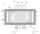
図2に、半導体装置2の断面図を示す。図2を参照して半導体装置2の概要を説明する。半導体装置2の詳細については、後に図3-図5を参照しつつ説明する。 FIG. 2 shows a cross-sectional view of the
冷却器3は樹脂で作られた四角筒状を成しており、その内部は冷媒が通る流路Pになっている。冷却器3は、四角筒状の外筒30と、外筒30の内側に掛け渡された複数の梁31を備えている。筒状の冷却器3の内部に複数の半導体モジュール10が固定されている。複数の半導体モジュール10は、筒状の冷却器3の筒軸線方向(図中の座標系のX方向)で間隔を空けて並んで配置されている。扁平な半導体モジュール10は、その幅狭の四面が筒状の冷却器3の内側に接合されている。別言すれば扁平な半導体モジュール10は、幅広面の法線方向からみて周囲が筒状の冷却器3の内側に接合されている。半導体モジュール10の図中座標系のY方向の両端は、梁31に接合されている。後に説明するが、Z方向の両端は外筒30の内側に接合されている。 The
各半導体モジュール10のパッケージ12の幅広面には、絶縁シート16を挟んで冷却板20が取り付けられている。冷却板20の流路Pに面する側には複数のピンフィン21が設けられている。なお、図2では、最上端と最下端の絶縁シートと冷却板とフィンにのみ符号を付し、他の絶縁シートと冷却板とフィンには符号を省略した。 A
冷却器3には冷媒供給口3aと冷媒排出口3bが設けられている。図2の矢印線が冷媒の流れを示している。冷媒は液体であり、典型的には水あるいはLLC(Long Life Coolant)である。冷媒供給口3aから流入した冷媒は、流路Pを通って冷却板20のピンフィン21の間を通り、半導体モジュール10から熱を吸収する。熱を吸収した冷媒は、冷媒排出口3bから排出される。扁平なパッケージ12の両方の幅広面にフィン付の冷却板20が取り付けられており、ピンフィン21の間を冷媒が通るので、半導体装置2は半導体モジュール10の冷却効率がよい。 The
図3-図5を参照して半導体装置2の構造を説明する。図3に、図2の破線IIIの範囲を抽出した部分断面図を示し、図4に、図3における矢印IVの方向からみた半導体装置2を示す。図5に、図4のV-V線に沿った断面図を示す。なお、図3-図5では、理解を助けるために、半導体モジュール10の部品の一部の縦横比をデフォルメして描いてある。 The structure of the
先に述べたように、半導体モジュール10は、樹脂製のパッケージ12の内部に2個の半導体素子4a、4bを封止したデバイスである。パッケージ12の材料には、例えばエポシキなどの熱硬化性樹脂に無機物を混合した樹脂材が用いられる。半導体素子4a、4bも扁平であり、一方の幅広面に平面状のコレクタ電極が設けられており、他方の幅広面に平面状のエミッタ電極と制御電極が設けられている。制御電極は、ゲート電極や、半導体素子4a、4bに内蔵された温度センサ用の端子である。 As described above, the
扁平なパッケージ12の一方の幅広面には放熱板13が露出しており、他方の面には放熱板15a、15bが露出している。放熱板13の裏側(パッケージ12に埋設されている側)には、半導体素子4aのエミッタ電極と半導体素子4bのコレクタ電極が接合されている。即ち、放熱板13は、半導体素子4a、4bを直列に接続する接続導体の役割を果たす。半導体素子4aのコレクタ電極は銅製のスペーサ14を介して放熱板15aと接続している。半導体素子4bのエミッタ電極は銅製のスペーサ14を介して放熱板15bと接続している。半導体素子4a、4bと放熱板13、15a、15bとの接合、及び、スペーサ14との接合には、ハンダが用いられる。 The
図5に示すように、放熱板13とパワー端子19aは、パッケージ12の内部で連続している。即ち、2個の半導体素子4a、4bの直列接続の中点は、放熱板13を介してパワー端子19aに接続している。図示は省略するが、同様に、2個の半導体素子4a、4bの直列接続の高電位側は、放熱板15aを介してパワー端子19bに接続しており、低電位側は放熱板15bを介してパワー端子19bに接続している。このように放熱板13、15a、15bは、半導体素子4a、4bの電極と導通しており、半導体素子4a、4bの内部の熱は、電極を介して放熱板13、15a、15bによく伝わる。半導体素子4aの制御電極と制御端子41は、パッケージ12の内部にて、ボンディングワイヤ42で接続される。半導体素子4bの制御電極も同様にボンディングワイヤで制御端子と接続される。 As shown in FIG. 5, the
パッケージ12の一方の幅広面には、放熱板15a、15bを覆うように、絶縁シート16aが貼着されている。他方の幅広面には、放熱板13を覆うように、絶縁シート16bが貼着されている。絶縁シート16a、16bは、エポシキ樹脂をベースに窒化ホウ素、アルミナを含んだ材料で作られている。絶縁シート16aは、当初は液状であり、放熱板15a、15bを覆うように幅広面に塗布される。液状の絶縁材は硬化し、絶縁シート16aとなる。絶縁シート16bも同様である。以下では、絶縁シート16a、16bの一方を区別なく示すときには絶縁シート16と表記する。 An insulating
パッケージ12の夫々の幅広面には、冷却板20が接合されている。冷却板20は、絶縁シート16を覆うとともに、絶縁シート16の周囲でパッケージ12の幅広面に接合されている。冷却板20は、伝熱材料が混在された樹脂で作られている。ベースとなる樹脂は、例えば、エポキシ樹脂である。エポキシ樹脂に混在させる伝熱材料は、例えば、鱗片状黒鉛、グラフェン、高熱伝導性カーボンファイバなどである。冷却板20とパッケージ12の接合には、大気圧プラズマ接合法が用いられる。冷却板20とパッケージ12の接合には、官能基としてアミン、チオール、シリコンを有する界面処理剤を用いた界面接合法が用いられても良い。 A cooling
冷却板20のパッケージ12と接合される面の反対側には、複数のピンフィン21が設けられている。冷却板20とピンフィン21は、絶縁シート16を貼着したパッケージ12を金型に入れ、その金型のキャビティに、伝熱材料を混在させた樹脂コンポジットを流し込んで成形される。このときの成形圧力は、パッケージ12にダメージを与えないように、例えば、10[MPa]未満に調整されるとよい。また、金型温度は、210℃未満であることが好ましい。ピンフィン21が設けられた冷却板20は、トランスファー成形、射出成形、圧縮成型などの手法で成形される。 A plurality of
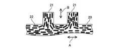
ここで、冷却板20に混在されている伝熱材料の配向について説明する。図6に、図3の破線VIの範囲の拡大図を示す。図6では、樹脂ベースに混在されている伝熱材料22を黒太線で示してある。伝熱材料22は、細長の針状である。伝熱材料22は、冷却板20の板の内部では、冷却板20の板面と平行な方向(図中の矢印Aの方向)に配向している。ピンフィン21の内部においては、伝熱材料22は、ピンフィン21の根本から先端に向かう方向(図中の矢印Bの方向)に配向している。冷却板20は、伝熱材料22の配向方向で伝熱特性が高くなる。伝熱材料22は、冷却板20の板の内部では板面の広がり方向に配向しており、ピンフィン21の内部ではピンフィン21の根本から先端に向かう方向に配向している。この配向によって、冷却板20の板内の熱はピンフィン21の先端へと伝わり易くなる。 Here, the orientation of the heat transfer material mixed in the
図3-図5に戻り、冷却器3について説明する。先に述べたように、冷却器3は、四角筒状の外筒30と、外筒30の内部に設けられた複数の梁31を備えている。なお、図4では、理解を助けるために、梁31はグレーで示してある。1個の半導体モジュール10に対して一対の梁31が対応している。図3と図4に示すように、一対の梁31の夫々は、両端が四角筒状の外筒30の内面に接合している。一対の梁31の間に半導体モジュール10が配置されている。扁平な半導体モジュール10(パッケージ12)の図中の座標系のY方向の両端が梁31に接合されており、Z方向の両端が外筒30の内面に接合されている。パッケージ12の幅広面の法線方向からみてパッケージ12の周囲が冷却器3に接合されており、パワー端子19a、19b、19cと制御端子41は、外筒30を貫通して外筒30の外側へと延びている。 FIG. 3-Returns to FIG. 5, and the
冷却器3は、樹脂で作られている。冷却器3の材料は、例えば、エポキシ系の樹脂である。なお、外筒30は、図中の座標系のX方向で複数の筒ブロックに分割されており、隣接する筒ブロックは、液漏れ防止のガスケット(不図示)を挟んで接合される。なお、図では複数のブロックを1個の外筒30として描いてある。外筒30は、半導体モジュール10と同数のブロックに分割される。そして、1個の半導体モジュール10に対して1個のブロックが成形される。冷却器3の各ブロックは、冷却板20を形成した半導体モジュール10を金型に入れ、溶融樹脂を流し込んで作られる。 The
冷却器3を形成する金型内では、冷却板20は、フローティング金型によって、冷却器3を成形するキャビティから隔離される。その結果、図4に示されているように、冷却板20の法線方向からみたときに、冷却板20の周囲と冷却器3の内面との間には、距離dWの隙間が確保される。別言すれば、冷却板20の法線方向からみて冷却板20の周囲の縁は冷却器3の内面から距離dWだけ離間している。なお、冷却板20はキャビティから必ずしも完全に隔離されていなくてもよい。別言すれば、冷却板20はその一部が冷却器3に接触していてもよい。 In the mold forming the
冷却器3を成形するときの条件は任意であるが、例えば、金型温度は、210℃以下に抑えられる。溶融した樹脂を金型内で固化させる際、樹脂の架橋密度を100%に近づけるため180℃以上かつ3時間以上の熱処理を行うとよい。そのような処理と、冷却板20が冷却器3から離間していることによって、冷却器3を成形するときの熱収縮にも関わらず、冷却板20に発生する内部応力が低く抑えられる。 The conditions for molding the
図中のY方向にて梁31と外筒30の間の空間が流路Pに相当する。先に図2を参照して説明したように、冷却器3の外部から供給される冷媒は流路Pを通じて冷却板20のピンフィン21の間に流れ、流路Pを通じて冷却器3の外部へと排出される。 The space between the
半導体装置2の利点を説明する。半導体装置2では、半導体モジュール10のパッケージ12に接合する冷却板20の材料として、金属製ではなく伝熱材料を混在させた樹脂を採用した。半導体モジュール10のパッケージ12も樹脂で作られているため、樹脂製の冷却板20とパッケージ12の接合性がよい。また、金属製の冷却板と比較して、樹脂製の冷却板20はパッケージ12との線膨張係数の差が大きくない。それゆえ、冷却板20の成形時の熱、冷却器3の成形時の熱、及び、半導体装置2の稼働中の熱サイクルに対して、冷却板20とパッケージ12の接合部分に発生する応力は小さい。それゆえ、冷却板20はパッケージ12から剥がれ難く、冷却性能の経時劣化が小さい。 The advantages of the
冷却板20の法線方向(図中のX方向)からみて、冷却板20の周囲の縁は、冷却器3から離間している。この特徴により、冷却器3の成形時の熱に関わらず冷却板20には熱応力が発生しない。このことも、冷却板20が剥がれ難くなることに貢献する。 The peripheral edge of the cooling
冷却板20は、細長形状の伝熱材料が混在している樹脂で作られている。伝熱材料は、ピンフィン21の内部には、ピンフィン21の根本から先端に向かう方向に配向している。この配向により、冷却板20の熱はピンフィン21の先端に伝わり易くなっている。 The cooling
実施例で説明した技術に関する留意点を述べる。冷却板20にはピンフィン21が設けられている。ピンフィンの代わりに板状のフィンであってもよい。実施例の半導体装置2では、半導体モジュール10の幅広面の法線方向からみて、パッケージ12の周囲が全て冷却器3に接合している。パッケージ12は、法線方向からみて少なくとも一対の両端が冷却器に接合していればよい。 The points to be noted regarding the technique described in the examples will be described. The cooling
半導体モジュール10に封止される半導体素子は1個でもよく、3個以上であってもよい。実施例の半導体装置2では、半導体モジュール10の一対の幅広面のそれぞれに放熱板が露出しており、冷却板20が接合されている。半導体モジュールの少なくとも一面に放熱板が露出しているとともに冷却板が接合されていればよい。冷却器3に内蔵される半導体モジュールの数にも制限はない。 The number of semiconductor elements sealed in the
以上、本発明の具体例を詳細に説明したが、これらは例示に過ぎず、特許請求の範囲を限定するものではない。特許請求の範囲に記載の技術には、以上に例示した具体例を様々に変形、変更したものが含まれる。本明細書または図面に説明した技術要素は、単独であるいは各種の組合せによって技術的有用性を発揮するものであり、出願時請求項記載の組合せに限定されるものではない。また、本明細書または図面に例示した技術は複数目的を同時に達成し得るものであり、そのうちの一つの目的を達成すること自体で技術的有用性を持つものである。 Although specific examples of the present invention have been described in detail above, these are merely examples and do not limit the scope of claims. The techniques described in the claims include various modifications and modifications of the specific examples exemplified above. The technical elements described herein or in the drawings exhibit their technical usefulness alone or in various combinations, and are not limited to the combinations described in the claims at the time of filing. In addition, the techniques exemplified in the present specification or the drawings can achieve a plurality of purposes at the same time, and achieving one of the purposes itself has technical usefulness.
2:半導体装置
3:冷却器
4a、4b:半導体素子
10:半導体モジュール
12:パッケージ
13、15a、15b:放熱板
14:スペーサ
16、16a、16b:絶縁シート
19a、19b、19c:パワー端子
20:冷却板
21:ピンフィン
22:伝熱材料
30:外筒
31:梁
41:制御端子
42:ボンディングワイヤ2: Semiconductor device 3:
Claims (3)
Translated fromJapanese伝熱材料が混在された樹脂で作られている冷却板であって、一方の面が前記パッケージの前記一面に接合されており、他方の面にフィンが設けられている冷却板と、
前記フィンに沿って冷媒を流す樹脂製の冷却器であって、前記冷却板の法線方向からみて前記冷却板を囲んでいるとともに、前記法線方向からみて前記パッケージの両端に接合されている冷却器と、
を備え、
前記冷却板は、前記冷却器から離間している、
半導体装置。A semiconductor module in which a semiconductor element is sealed inside a resin package and a heat sink is exposed on at least one surface.
A cooling plate made of a resin mixed with aheat transfer material, one of which is joined to the one sideof the package and the other side of which is provided with fins.
A resin cooler in which a refrigerant flows along the fins, which surrounds the cooling plate when viewed from the normal direction of the cooling plate, and is joined to both ends of the package when viewed from the normal direction. With a cooler,
Equippedwith
The cooling plate is separated from the cooler.
Semiconductor device.
Priority Applications (3)
| Application Number | Priority Date | Filing Date | Title |
|---|---|---|---|
| JP2017185098AJP7039908B2 (en) | 2017-09-26 | 2017-09-26 | Semiconductor device |
| US16/113,431US10600720B2 (en) | 2017-09-26 | 2018-08-27 | Semiconductor device |
| CN201811107491.4ACN109560049B (en) | 2017-09-26 | 2018-09-21 | Semiconductor device with a plurality of semiconductor chips |
Applications Claiming Priority (1)
| Application Number | Priority Date | Filing Date | Title |
|---|---|---|---|
| JP2017185098AJP7039908B2 (en) | 2017-09-26 | 2017-09-26 | Semiconductor device |
Publications (2)
| Publication Number | Publication Date |
|---|---|
| JP2019062066A JP2019062066A (en) | 2019-04-18 |
| JP7039908B2true JP7039908B2 (en) | 2022-03-23 |
Family
ID=65809358
Family Applications (1)
| Application Number | Title | Priority Date | Filing Date |
|---|---|---|---|
| JP2017185098AActiveJP7039908B2 (en) | 2017-09-26 | 2017-09-26 | Semiconductor device |
Country Status (3)
| Country | Link |
|---|---|
| US (1) | US10600720B2 (en) |
| JP (1) | JP7039908B2 (en) |
| CN (1) | CN109560049B (en) |
Families Citing this family (8)
| Publication number | Priority date | Publication date | Assignee | Title |
|---|---|---|---|---|
| US11355418B2 (en)* | 2019-09-29 | 2022-06-07 | Taiwan Semiconductor Manufacturing Company, Ltd. | Package structure and manufacturing method thereof |
| CN110993576B (en)* | 2019-12-23 | 2021-10-15 | 西安华为技术有限公司 | Heat dissipation device and communication equipment |
| JP7404107B2 (en)* | 2020-02-27 | 2023-12-25 | 三菱重工業株式会社 | Cooling system |
| DE102020112809A1 (en)* | 2020-05-12 | 2021-11-18 | Lisa Dräxlmaier GmbH | Cooling arrangement |
| JP7355707B2 (en)* | 2020-05-13 | 2023-10-03 | 日立Astemo株式会社 | Semiconductor equipment, busbars and power conversion equipment |
| CN113114021B (en)* | 2021-04-07 | 2022-05-13 | 台达电子企业管理(上海)有限公司 | Driving system of power device |
| KR20240105891A (en)* | 2022-12-29 | 2024-07-08 | 현대자동차주식회사 | Power module |
| TWI881284B (en)* | 2023-02-01 | 2025-04-21 | 緯創資通股份有限公司 | Cold plate and electronic device including the same |
Citations (3)
| Publication number | Priority date | Publication date | Assignee | Title |
|---|---|---|---|---|
| JP2014229714A (en) | 2013-05-21 | 2014-12-08 | 宇部興産機械株式会社 | Heat radiation structure and manufacturing method of the same |
| CN104956480A (en) | 2012-10-29 | 2015-09-30 | Tp视觉控股有限公司 | Heat conductor device and method of forming a heat conductor device |
| JP2016131196A (en) | 2015-01-13 | 2016-07-21 | トヨタ自動車株式会社 | Semiconductor device |
Family Cites Families (6)
| Publication number | Priority date | Publication date | Assignee | Title |
|---|---|---|---|---|
| JPH04291948A (en)* | 1991-03-20 | 1992-10-16 | Fujitsu Ltd | Semiconductor device and its manufacture; radiating fin |
| US8125781B2 (en)* | 2004-11-11 | 2012-02-28 | Denso Corporation | Semiconductor device |
| JP6295238B2 (en)* | 2014-10-31 | 2018-03-14 | デクセリアルズ株式会社 | HEAT CONDUCTIVE SHEET, HEAT CONDUCTIVE SHEET MANUFACTURING METHOD, HEAT DISSIBLING MEMBER AND SEMICONDUCTOR DEVICE |
| JP6424573B2 (en) | 2014-11-06 | 2018-11-21 | トヨタ自動車株式会社 | Semiconductor device |
| JP2016111089A (en) | 2014-12-03 | 2016-06-20 | トヨタ自動車株式会社 | Semiconductor device |
| JP6281506B2 (en)* | 2015-02-24 | 2018-02-21 | トヨタ自動車株式会社 | Semiconductor module |
- 2017
- 2017-09-26JPJP2017185098Apatent/JP7039908B2/enactiveActive
- 2018
- 2018-08-27USUS16/113,431patent/US10600720B2/enactiveActive
- 2018-09-21CNCN201811107491.4Apatent/CN109560049B/enactiveActive
Patent Citations (4)
| Publication number | Priority date | Publication date | Assignee | Title |
|---|---|---|---|---|
| CN104956480A (en) | 2012-10-29 | 2015-09-30 | Tp视觉控股有限公司 | Heat conductor device and method of forming a heat conductor device |
| JP2015535392A (en) | 2012-10-29 | 2015-12-10 | ティーピー ビジョン ホールディング ビー ヴィ | Thermally conductive element and method for forming the thermally conductive element |
| JP2014229714A (en) | 2013-05-21 | 2014-12-08 | 宇部興産機械株式会社 | Heat radiation structure and manufacturing method of the same |
| JP2016131196A (en) | 2015-01-13 | 2016-07-21 | トヨタ自動車株式会社 | Semiconductor device |
Also Published As
| Publication number | Publication date |
|---|---|
| US20190096784A1 (en) | 2019-03-28 |
| CN109560049A (en) | 2019-04-02 |
| CN109560049B (en) | 2023-02-17 |
| JP2019062066A (en) | 2019-04-18 |
| US10600720B2 (en) | 2020-03-24 |
Similar Documents
| Publication | Publication Date | Title |
|---|---|---|
| JP7039908B2 (en) | Semiconductor device | |
| KR101956996B1 (en) | Power module of double-side cooling | |
| JP6120704B2 (en) | Semiconductor device | |
| JP5656907B2 (en) | Power module | |
| CN103650137B (en) | Power semiconductor modular | |
| JP5472498B2 (en) | Power module manufacturing method | |
| EP3343603B1 (en) | Structure | |
| JP2015220382A (en) | Power module | |
| US20160111345A1 (en) | Semiconductor module, semiconductor device, and vehicle | |
| US10064310B2 (en) | Power-module device, power conversion device, and method for manufacturing power-module device | |
| CN108735692A (en) | Semiconductor device | |
| CN107112316A (en) | Semiconductor module | |
| US20150130042A1 (en) | Semiconductor module with radiation fins | |
| JP2011216564A (en) | Power module and method of manufacturing the same | |
| JP7463825B2 (en) | Semiconductor modules and vehicles | |
| WO2020105075A1 (en) | Semiconductor device | |
| CN220856564U (en) | Power module | |
| JP2015126168A (en) | Power module | |
| JP2015133402A (en) | Semiconductor module manufacturing method | |
| JP2008311550A (en) | Power semiconductor module | |
| CN104126225A (en) | Semiconductor device | |
| JP6286541B2 (en) | Power module device and power conversion device | |
| WO2014045758A1 (en) | Power semiconductor module | |
| CN111081664B (en) | Package of semiconductor device with phase change material for thermal performance | |
| JP2019040955A (en) | Manufacturing method of semiconductor module |
Legal Events
| Date | Code | Title | Description |
|---|---|---|---|
| A711 | Notification of change in applicant | Free format text:JAPANESE INTERMEDIATE CODE: A711 Effective date:20200401 | |
| A621 | Written request for application examination | Free format text:JAPANESE INTERMEDIATE CODE: A621 Effective date:20200812 | |
| A977 | Report on retrieval | Free format text:JAPANESE INTERMEDIATE CODE: A971007 Effective date:20210712 | |
| A131 | Notification of reasons for refusal | Free format text:JAPANESE INTERMEDIATE CODE: A131 Effective date:20210720 | |
| A521 | Request for written amendment filed | Free format text:JAPANESE INTERMEDIATE CODE: A523 Effective date:20210914 | |
| TRDD | Decision of grant or rejection written | ||
| A01 | Written decision to grant a patent or to grant a registration (utility model) | Free format text:JAPANESE INTERMEDIATE CODE: A01 Effective date:20220208 | |
| A61 | First payment of annual fees (during grant procedure) | Free format text:JAPANESE INTERMEDIATE CODE: A61 Effective date:20220221 | |
| R151 | Written notification of patent or utility model registration | Ref document number:7039908 Country of ref document:JP Free format text:JAPANESE INTERMEDIATE CODE: R151 | |
| R250 | Receipt of annual fees | Free format text:JAPANESE INTERMEDIATE CODE: R250 |