JP7038901B2 - Plasma sheath control for RF plasma reactor - Google Patents
Plasma sheath control for RF plasma reactorDownload PDFInfo
- Publication number
- JP7038901B2 JP7038901B2JP2021506927AJP2021506927AJP7038901B2JP 7038901 B2JP7038901 B2JP 7038901B2JP 2021506927 AJP2021506927 AJP 2021506927AJP 2021506927 AJP2021506927 AJP 2021506927AJP 7038901 B2JP7038901 B2JP 7038901B2
- Authority
- JP
- Japan
- Prior art keywords
- plasma
- control system
- plasma sheath
- sheath control
- switch
- Prior art date
- Legal status (The legal status is an assumption and is not a legal conclusion. Google has not performed a legal analysis and makes no representation as to the accuracy of the status listed.)
- Active
Links
Images


Classifications
- H—ELECTRICITY
- H01—ELECTRIC ELEMENTS
- H01J—ELECTRIC DISCHARGE TUBES OR DISCHARGE LAMPS
- H01J37/00—Discharge tubes with provision for introducing objects or material to be exposed to the discharge, e.g. for the purpose of examination or processing thereof
- H01J37/32—Gas-filled discharge tubes
- H01J37/32009—Arrangements for generation of plasma specially adapted for examination or treatment of objects, e.g. plasma sources
- H01J37/32082—Radio frequency generated discharge
- H01J37/32128—Radio frequency generated discharge using particular waveforms, e.g. polarised waves
- H—ELECTRICITY
- H01—ELECTRIC ELEMENTS
- H01J—ELECTRIC DISCHARGE TUBES OR DISCHARGE LAMPS
- H01J37/00—Discharge tubes with provision for introducing objects or material to be exposed to the discharge, e.g. for the purpose of examination or processing thereof
- H01J37/32—Gas-filled discharge tubes
- H01J37/32431—Constructional details of the reactor
- H—ELECTRICITY
- H02—GENERATION; CONVERSION OR DISTRIBUTION OF ELECTRIC POWER
- H02M—APPARATUS FOR CONVERSION BETWEEN AC AND AC, BETWEEN AC AND DC, OR BETWEEN DC AND DC, AND FOR USE WITH MAINS OR SIMILAR POWER SUPPLY SYSTEMS; CONVERSION OF DC OR AC INPUT POWER INTO SURGE OUTPUT POWER; CONTROL OR REGULATION THEREOF
- H02M3/00—Conversion of DC power input into DC power output
- H02M3/01—Resonant DC/DC converters
- H—ELECTRICITY
- H02—GENERATION; CONVERSION OR DISTRIBUTION OF ELECTRIC POWER
- H02M—APPARATUS FOR CONVERSION BETWEEN AC AND AC, BETWEEN AC AND DC, OR BETWEEN DC AND DC, AND FOR USE WITH MAINS OR SIMILAR POWER SUPPLY SYSTEMS; CONVERSION OF DC OR AC INPUT POWER INTO SURGE OUTPUT POWER; CONTROL OR REGULATION THEREOF
- H02M3/00—Conversion of DC power input into DC power output
- H02M3/22—Conversion of DC power input into DC power output with intermediate conversion into AC
- H02M3/24—Conversion of DC power input into DC power output with intermediate conversion into AC by static converters
- H02M3/28—Conversion of DC power input into DC power output with intermediate conversion into AC by static converters using discharge tubes with control electrode or semiconductor devices with control electrode to produce the intermediate AC
- H02M3/325—Conversion of DC power input into DC power output with intermediate conversion into AC by static converters using discharge tubes with control electrode or semiconductor devices with control electrode to produce the intermediate AC using devices of a triode or a transistor type requiring continuous application of a control signal
- H02M3/335—Conversion of DC power input into DC power output with intermediate conversion into AC by static converters using discharge tubes with control electrode or semiconductor devices with control electrode to produce the intermediate AC using devices of a triode or a transistor type requiring continuous application of a control signal using semiconductor devices only
- H02M3/33569—Conversion of DC power input into DC power output with intermediate conversion into AC by static converters using discharge tubes with control electrode or semiconductor devices with control electrode to produce the intermediate AC using devices of a triode or a transistor type requiring continuous application of a control signal using semiconductor devices only having several active switching elements
- H02M3/33571—Half-bridge at primary side of an isolation transformer
- H—ELECTRICITY
- H02—GENERATION; CONVERSION OR DISTRIBUTION OF ELECTRIC POWER
- H02M—APPARATUS FOR CONVERSION BETWEEN AC AND AC, BETWEEN AC AND DC, OR BETWEEN DC AND DC, AND FOR USE WITH MAINS OR SIMILAR POWER SUPPLY SYSTEMS; CONVERSION OF DC OR AC INPUT POWER INTO SURGE OUTPUT POWER; CONTROL OR REGULATION THEREOF
- H02M3/00—Conversion of DC power input into DC power output
- H02M3/22—Conversion of DC power input into DC power output with intermediate conversion into AC
- H02M3/24—Conversion of DC power input into DC power output with intermediate conversion into AC by static converters
- H02M3/28—Conversion of DC power input into DC power output with intermediate conversion into AC by static converters using discharge tubes with control electrode or semiconductor devices with control electrode to produce the intermediate AC
- H02M3/325—Conversion of DC power input into DC power output with intermediate conversion into AC by static converters using discharge tubes with control electrode or semiconductor devices with control electrode to produce the intermediate AC using devices of a triode or a transistor type requiring continuous application of a control signal
- H02M3/335—Conversion of DC power input into DC power output with intermediate conversion into AC by static converters using discharge tubes with control electrode or semiconductor devices with control electrode to produce the intermediate AC using devices of a triode or a transistor type requiring continuous application of a control signal using semiconductor devices only
- H02M3/33569—Conversion of DC power input into DC power output with intermediate conversion into AC by static converters using discharge tubes with control electrode or semiconductor devices with control electrode to produce the intermediate AC using devices of a triode or a transistor type requiring continuous application of a control signal using semiconductor devices only having several active switching elements
- H02M3/33573—Full-bridge at primary side of an isolation transformer
- H—ELECTRICITY
- H03—ELECTRONIC CIRCUITRY
- H03K—PULSE TECHNIQUE
- H03K3/00—Circuits for generating electric pulses; Monostable, bistable or multistable circuits
- H03K3/02—Generators characterised by the type of circuit or by the means used for producing pulses
- H03K3/53—Generators characterised by the type of circuit or by the means used for producing pulses by the use of an energy-accumulating element discharged through the load by a switching device controlled by an external signal and not incorporating positive feedback
- H03K3/57—Generators characterised by the type of circuit or by the means used for producing pulses by the use of an energy-accumulating element discharged through the load by a switching device controlled by an external signal and not incorporating positive feedback the switching device being a semiconductor device
- H—ELECTRICITY
- H02—GENERATION; CONVERSION OR DISTRIBUTION OF ELECTRIC POWER
- H02M—APPARATUS FOR CONVERSION BETWEEN AC AND AC, BETWEEN AC AND DC, OR BETWEEN DC AND DC, AND FOR USE WITH MAINS OR SIMILAR POWER SUPPLY SYSTEMS; CONVERSION OF DC OR AC INPUT POWER INTO SURGE OUTPUT POWER; CONTROL OR REGULATION THEREOF
- H02M1/00—Details of apparatus for conversion
- H02M1/08—Circuits specially adapted for the generation of control voltages for semiconductor devices incorporated in static converters
- H02M1/088—Circuits specially adapted for the generation of control voltages for semiconductor devices incorporated in static converters for the simultaneous control of series or parallel connected semiconductor devices
Landscapes
- Engineering & Computer Science (AREA)
- Physics & Mathematics (AREA)
- Plasma & Fusion (AREA)
- Chemical & Material Sciences (AREA)
- Analytical Chemistry (AREA)
- Power Engineering (AREA)
- Plasma Technology (AREA)
- Drying Of Semiconductors (AREA)
- Physical Vapour Deposition (AREA)
Description
Translated fromJapanese(関連出願の相互参照)
本出願は、2018年8月10日に出願された、「プラズマリアクタ用プラズマシース制御(PLASMA SHEATH CONTROL FOR RF PLASMA REACTORS)」という名称の米国仮特許出願第62/717,523号の優先権を主張するものであり、この仮特許出願の全体が参照により本明細書に組み込まれる。
本出願は、2018年11月30日に出願された、「可変出力インピーダンスRF発生器(VARIABLE OUTPUT IMPEDANCE RF GENERATOR)」という名称の米国仮特許出願第62/774,078号の優先権を主張するものであり、この仮特許出願の全体が参照により本明細書に組み込まれる。
本出願は、2019年1月8日に出願された、「ナノ秒パルサー回路における効率的なエネルギー回収(EFFICIENT ENERGY RECOVERY IN A NANOSECOND PULSER CIRCUIT)」という名称の米国仮特許出願第62/789,523号の優先権を主張するものであり、この仮特許出願の全体が参照により本明細書に組み込まれる。
本出願は、2019年1月8日に出願された、「プラズマ制御用途向けのソース及びシンク能力を備えた効率的ナノ秒パルサー(EFFICIENT NANOSECOND PULSER WITH SOURCE AND SINK CAPABILITY FOR PLASMA CONTROL APPLICATIONS)」という名称の米国仮特許出願第62/789,526号の優先権を主張するものであり、この仮特許出願の全体が参照により本明細書に組み込まれる。(Mutual reference of related applications)
This application gives priority to the US provisional patent application No. 62 / 717,523, entitled "Plasma Sheath Control for Plasma Reactor (PLASMA SHEATH CONTROL FOR RF PLASMA REACTORS)" filed on August 10, 2018. It is alleged that the entire provisional patent application is incorporated herein by reference.
This application claims the priority of US Provisional Patent Application No. 62 / 774,078, filed November 30, 2018, entitled "VARIABLE OUTPUT IMPEDANCE RF GENERATIONR". As a matter of fact, the entire provisional patent application is incorporated herein by reference.
This application is filed on January 8, 2019, and is a US provisional patent application entitled "EFFICIENT ENERGY RECOVERY IN A NANOSECOND PULSER CIRCUIT". It claims the priority of the issue and the entire provisional patent application is incorporated herein by reference.
This application was filed on January 8, 2019, "EffICCIENT NANOSECOND PULSER WITH SOURCE AND SINK CAPAVIITY FOR PLASMA CONTROL APPLICIONS with source and sink capabilities for plasma control applications". Claims priority in US Provisional Patent Application No. 62 / 789,526, which is incorporated herein by reference in its entirety.
本発明は、RFプラズマリアクタ用プラズマシース制御に関する。 The present invention relates to plasma sheath control for RF plasma reactors.
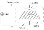
薄膜製造技術におけるRF励起ガス放電の適用は標準的になっている。最も一般的に使用されている最も単純な形状は、電圧が印加される2つの平面電極の間にあるものである。このような平面状のRFプラズマリアクタの模式図を図1に示す。プラズマは、プラズマシースによって各電極から分離されている。 The application of RF-excited gas discharge in thin film manufacturing techniques has become standard. The simplest shape most commonly used is between two plane electrodes to which a voltage is applied. A schematic diagram of such a planar RF plasma reactor is shown in FIG. The plasma is separated from each electrode by a plasma sheath.
プラズマ中で生成された正イオンは、プラズマシースに亘って加速され、シースに亘る時間依存性の電位差の大きさと波形、ガス圧、リアクタの物理的形状、及び/又は他の要因によって決定されるイオンエネルギー分布関数(IEDF)で電極に到達する。このイオン衝撃エネルギー分布は、薄膜エッチングにおける異方性の程度、表面へのイオン衝撃による損傷の程度等を決定し得る。 Positive ions generated in the plasma are accelerated across the plasma sheath and are determined by the magnitude and waveform of the time-dependent potential difference across the sheath, the gas pressure, the physical shape of the reactor, and / or other factors. It reaches the electrode by the ion energy distribution function (IEDF). This ion impact energy distribution can determine the degree of anisotropy in thin film etching, the degree of damage due to ion impact on the surface, and the like.
幾つかの実施形態では、20kHzを超える周波数及び1kVを超えるピーク電圧を有するRF正弦波形を生成するRF電源と、RF電源と電気的に結合されたプラズマチャンバとを含むプラズマシース制御システムを含み、プラズマチャンバは、配置された面内に、約1kVを超えるエネルギーで加速される複数のイオンを有し、又、プラズマチャンバは、RF正弦波形からプラズマチャンバ内にプラズマシースを生成する。プラズマシース制御システムは、RF電源とプラズマチャンバとの間に電気的に結合されたブロッキングダイオードと、RF電源、プラズマチャンバ、及びブロッキングダイオードと電気的に結合された容量性放電回路とを含み、容量性放電回路は、1kVを超えるピーク電圧及び250ナノ秒未満の放電時間でプラズマチャンバ内の容量性電荷を放電する。 Some embodiments include a plasma sheath control system comprising an RF power source that produces an RF sinusoidal waveform with a frequency above 20 kHz and a peak voltage above 1 kV, and a plasma chamber electrically coupled to the RF power supply. The plasma chamber has a plurality of ions in the arranged plane that are accelerated by an energy of more than about 1 kV, and the plasma chamber creates a plasma sheath in the plasma chamber from the RF sinusoidal waveform. The plasma sheath control system includes a blocking diode electrically coupled between the RF power supply and the plasma chamber, and a capacitive discharge circuit electrically coupled to the RF power supply, the plasma chamber, and the blocking diode. The sex discharge circuit discharges the capacitive charge in the plasma chamber with a peak voltage of more than 1 kV and a discharge time of less than 250 nanoseconds.
幾つかの実施形態では、容量性放電回路は、直列に配置された抵抗器とインダクタを備えた抵抗出力段を備え、抵抗出力段は、プラズマシース制御システム上のブロッキングダイオードとプラズマチャンバとの間の点と接地との間に配置されている。 In some embodiments, the capacitive discharge circuit comprises a resistance output stage with a resistor and inductor arranged in series, and the resistance output stage is between the blocking diode and the plasma chamber on the plasma sheath control system. It is placed between the point and the ground.
幾つかの実施形態では、容量性放電回路は、直列に配置されたダイオードとインダクタを備えたエネルギー回収回路を備え、エネルギー回収回路は、ブロッキングダイオードとプラズマチャンバとRF電源との間に配置されている。 In some embodiments, the capacitive discharge circuit comprises an energy recovery circuit with a diode and inductor placed in series, and the energy recovery circuit is placed between the blocking diode, the plasma chamber, and the RF power supply. There is.
幾つかの実施形態では、プラズマシース制御システムは、ブロッキングダイオードとプラズマチャンバとの間に直列に配置されたバイアスコンデンサを含んでもよい。幾つかの実施形態では、プラズマシース制御システムは、直流電源、抵抗器、ダイオード及び高電圧スイッチを備えたバイアス補償回路を含んでもよく、バイアス補償回路は、プラズマシース制御システム上のブロッキングダイオードとRF電源との間の点の間に配置されている。 In some embodiments, the plasma sheath control system may include a bias capacitor placed in series between the blocking diode and the plasma chamber. In some embodiments, the plasma sheath control system may include a bias compensation circuit with a DC power supply, a resistor, a diode and a high voltage switch, the bias compensation circuit being a blocking diode and RF on the plasma sheath control system. It is located between the points between the power supplies.
幾つかの実施形態では、プラズマシース制御システムは、プラズマチャンバと電気的に結合されたマッチングネットワークを含んでもよく、マッチングネットワークは、プラズマチャンバ内のプラズマ負荷の反応性インピーダンスをRF電源の出力インピーダンスに一致させる。 In some embodiments, the plasma sheath control system may include a matching network that is electrically coupled to the plasma chamber, where the matching network translates the reactive impedance of the plasma load in the plasma chamber into the output impedance of the RF power supply. Match.
幾つかの実施形態では、ブロッキングダイオードは、正弦波形を整流して、各周期の少なくとも25%に実質的に平坦な部分を有する正弦波形を作成する。 In some embodiments, the blocking diode rectifies the sinusoidal waveform to create a sinusoidal waveform with a substantially flat portion at least 25% of each period.
幾つかの実施形態はプラズマシース制御システムを含む。プラズマシース制御システムは、200Vを超える直流電圧を生成する高圧直流電源を含んでもよい。プラズマシース制御システムは共振回路ドライバを含んでもよく、共振回路ドライバはオンとオフに交互に切り替わって20kHzを超える周波数及び1kVを超えるピーク電圧を有する正弦波形を生成する、共振負荷に結合された複数の高電圧スイッチを備えている。プラズマシース制御システムは、共振回路ドライバと電気的に結合されたプラズマチャンバを含んでもよく、プラズマチャンバは、プラズマチャンバ内に配置された面に約1kVを超えるエネルギーで加速される複数のイオンを有し、プラズマチャンバは、正弦波形から、プラズマチャンバ内にプラズマシースを生成する。プラズマシース制御システムは、共振回路ドライバとプラズマチャンバとの間に電気的に接続された、正弦波形を整流するブロッキングダイオードを含んでもよい。 Some embodiments include a plasma sheath control system. The plasma sheath control system may include a high voltage DC power source that produces a DC voltage in excess of 200 V. The plasma sheath control system may include a resonant circuit driver, which alternates on and off to produce a sinusoidal waveform with a frequency above 20 kHz and a peak voltage above 1 kV, coupled to a resonant load. Equipped with a high voltage switch. The plasma sheath control system may include a plasma chamber electrically coupled with a resonant circuit driver, which has multiple ions on a surface located within the plasma chamber that are accelerated with an energy of greater than about 1 kV. However, the plasma chamber creates a plasma sheath in the plasma chamber from the sine waveform. The plasma sheath control system may include a blocking diode that rectifies the sinusoidal waveform, which is electrically connected between the resonant circuit driver and the plasma chamber.
幾つかの実施形態では、ブロッキングダイオードは、正弦波形を整流して、各周期の少なくとも25%に実質的に平坦な部分を有する波形を作成する。 In some embodiments, the blocking diode rectifies a sinusoidal waveform to create a waveform with a substantially flat portion at least 25% of each period.
幾つかの実施形態では、プラズマシース制御システムは、直列に配置された抵抗器とインダクタを含む抵抗出力段を含んでもよく、抵抗出力段は、ブロッキングダイオードとプラズマチャンバとの間のプラズマシース制御システム上の点と接地との間に配置されている。 In some embodiments, the plasma sheath control system may include a resistance output stage that includes a resistor and inductor placed in series, where the resistance output stage is a plasma sheath control system between the blocking diode and the plasma chamber. It is located between the upper point and the ground.
幾つかの実施形態では、プラズマシース制御システムは、直列に配置されたダイオードとインダクタを含むエネルギー回収回路を含んでもよく、エネルギー回収回路は、ブロッキングダイオードとプラズマチャンバと高電圧直流電源との間に配置されている。 In some embodiments, the plasma sheath control system may include an energy recovery circuit that includes a diode and an inductor placed in series, the energy recovery circuit being between the blocking diode, the plasma chamber, and the high voltage DC power supply. Have been placed.
幾つかの実施形態では、複数のスイッチは、第1のスイッチ、第2のスイッチ、第3のスイッチ、及び第4のスイッチを含む。幾つかの実施形態では、第1のスイッチ及び第4のスイッチは第1の時間期間中に閉じて、第1の方向に電流を流すことを可能にし、第2のスイッチ及び第3のスイッチは第2の期間中に閉じて、第1の方向とは反対の第2の方向に電流を流すことを可能にする。 In some embodiments, the plurality of switches includes a first switch, a second switch, a third switch, and a fourth switch. In some embodiments, the first switch and the fourth switch are closed during the first time period to allow current to flow in the first direction, and the second and third switches are. It closes during the second period and allows current to flow in the second direction opposite to the first direction.
幾つかの実施形態では、複数のスイッチは、第1のスイッチと第2のスイッチを含む。幾つかの実施形態では、第1のスイッチは第1の時間期間中に閉じて、第1の方向に電流を流すことを可能にし、第2のスイッチは第2の期間中に閉じて、第1の方向とは反対の第2の方向に電流を流すことを可能にする。 In some embodiments, the plurality of switches includes a first switch and a second switch. In some embodiments, the first switch closes during the first time period to allow current to flow in the first direction, the second switch closes during the second period, and the second. It allows current to flow in a second direction opposite to one.
幾つかの実施形態では、複数のスイッチは、
幾つかの実施形態では、複数のスイッチは、
幾つかの実施形態では、複数のスイッチは、
幾つかの実施形態では、プラズマシース制御システムは、共振回路ドライバが正弦波形を生成している間に約1kVを超える電圧をプラズマシースに亘り生成する。 In some embodiments, the plasma sheath control system produces a voltage greater than about 1 kV over the plasma sheath while the resonant circuit driver produces a sinusoidal waveform.
幾つかの実施形態では、プラズマシース制御システムは、共振回路によって生成される正弦波形の周波数又はパワーの何れか又は両方を、約1ms未満の時間スケールで調整するコントローラを含んでもよい。 In some embodiments, the plasma sheath control system may include a controller that adjusts either or both of the frequencies and / or powers of the sinusoidal waveform produced by the resonant circuit on a time scale of less than about 1 ms.
幾つかの実施形態では、プラズマシース制御システムは、プラズマチャンバ以前の点における正弦波形の周波数を測定し、プラズマチャンバ以前の点における正弦波形の周波数が共振周波数と一致しない場合に、共振回路ドライバによって生成される正弦波形の周波数を調整するコントローラを含んでもよい。 In some embodiments, the plasma sheath control system measures the frequency of the sinusoidal waveform at the point prior to the plasma chamber, and if the frequency of the sinusoidal waveform at the point prior to the plasma chamber does not match the resonant frequency, the resonant circuit driver. It may include a controller that adjusts the frequency of the generated sine waveform.
幾つかの実施形態では、プラズマシース制御システムは、プラズマチャンバ以前の点における正弦波形のパワーを測定し、プラズマチャンバ以前の点における正弦波形のパワーが所要パワーと一致しない場合に、共振回路ドライバによって生成される正弦波形のパワーを調整するコントローラを含んでもよい。 In some embodiments, the plasma sheath control system measures the power of the sinusoidal waveform at the point prior to the plasma chamber, and if the power of the sinusoidal waveform at the point prior to the plasma chamber does not match the required power, by a resonant circuit driver. It may include a controller that adjusts the power of the generated sinusoidal waveform.
本発明の幾つかの実施形態は、高電圧及び高周波数正弦波形を生成するRF電源と、抵抗器及びインダクタを備えた抵抗出力段と、RF電源と抵抗出力段との間に配置されたブロッキングダイオードとを備えたプラズマシース制御システムを含む。幾つかの実施形態では、ガス供給システム、制御システム、プラズマ発生システム、真空ポンピング、ウェハ搬送システム等を含み得るプラズマリアクタが含まれ得る。幾つかの実施形態では、抵抗出力段は約200pF未満のキャパシタンスを有する。幾つかの実施形態では、プラズマシース制御システムは、ウェハ成膜デバイスと結合するように構成された出力を更に含む。幾つかの実施形態では、プラズマシース制御システムは更に、2kVを超える振幅及び1kHzを超える周波数を有する高電圧正弦波形を出力するように構成された出力を備えている。 Some embodiments of the present invention include an RF power supply that produces high voltage and high frequency sinusoidal waveforms, a resistance output stage with resistors and inductors, and blocking located between the RF power supply and the resistance output stage. Includes a plasma sheath control system with a diode. In some embodiments, plasma reactors may include a gas supply system, a control system, a plasma generation system, a vacuum pumping, a wafer transfer system, and the like. In some embodiments, the resistance output stage has a capacitance of less than about 200 pF. In some embodiments, the plasma sheath control system further comprises an output configured to couple with a wafer deposition device. In some embodiments, the plasma sheath control system further comprises an output configured to output a high voltage sinusoidal waveform having an amplitude greater than 2 kV and a frequency greater than 1 kHz.
本発明の幾つかの実施形態はプラズマシース制御システムを含み、プラズマシース制御システムは、RF電源と、バイアスコンデンサと、ブロッキングダイオードを跨いで結合された高電圧スイッチを含み、高電圧スイッチは、高電圧スイッチング電源がオンのときにオフであり、高電圧スイッチは、高電圧スイッチング電源がパルシングしていないときにはオンである。幾つかの実施形態では、プラズマシース制御システムは更に、ウェハ成膜デバイスと結合するように構成された出力を含む。幾つかの実施形態では、プラズマシース制御システムは更に、2kVを超える振幅と、1kHzを超える周波数を有する高電圧正弦波形を出力するように構成された出力を備えている。 Some embodiments of the present invention include a plasma sheath control system, the plasma sheath control system comprising an RF power supply, a bias capacitor, and a high voltage switch coupled across a blocking diode, the high voltage switch being high. The voltage switching power supply is off when it is on, and the high voltage switch is on when the high voltage switching power supply is not pulsing. In some embodiments, the plasma sheath control system further comprises an output configured to couple with a wafer deposition device. In some embodiments, the plasma sheath control system further comprises an output configured to output a high voltage sinusoidal waveform with an amplitude greater than 2 kV and a frequency greater than 1 kHz.
本発明の幾つかの実施形態は、プラズマシース制御システムがオンである期間とプラズマシース制御システムがオフである期間に、ウェハとチャックとの間の電圧電位が約2kVとなるようにウェハ成膜チャンバ内にプラズマを生成する出力を生成するプラズマシース制御システムを含む。 In some embodiments of the present invention, wafer deposition is performed so that the voltage potential between the wafer and the chuck is approximately 2 kV during the period when the plasma sheath control system is on and the period when the plasma sheath control system is off. Includes a plasma sheath control system that produces an output that produces plasma in the chamber.
幾つかの実施形態では、抵抗出力段は、受動コンポーネントの直列又は並列ネットワークを含んでもよい。例えば、抵抗出力段は、直列の抵抗器、コンデンサ、及びインダクタを含んでもよい。別の例として、抵抗出力段は、インダクタと並列のコンデンサと、抵抗器と直列のコンデンサ・インダクタの組み合わせを含んでもよい。配置に拘らず、コンポーネント値はRFソースのRF周波数に一致するように選択され得る。 In some embodiments, the resistance output stage may include a series or parallel network of passive components. For example, the resistance output stage may include resistors, capacitors, and inductors in series. As another example, the resistance output stage may include a capacitor in parallel with the inductor and a combination of capacitors and inductors in series with the resistor. Regardless of the placement, the component values can be selected to match the RF frequency of the RF source.
これらの例示的な実施形態は、本開示を限定したり定義したりする為ではなく、本開示の理解を助ける為の例を提供する為に言及されている。追加の実施形態は、「発明を実施するための形態」で議論され、そこでは更なる説明が提供される。様々な実施形態のうち1つ以上の実施形態によって提供される利点は、本明細書を検討することによって、又は提示された1つ以上の実施形態を実践することによって、更に理解され得る。 These exemplary embodiments are referred to not to limit or define the present disclosure, but to provide examples to aid in the understanding of the present disclosure. Additional embodiments are discussed in "Embodiments for Carrying Out the Invention", wherein further description is provided. The advantages provided by one or more of the various embodiments may be further understood by reviewing the present specification or by practicing one or more of the presented embodiments.
本開示のこれら及び他の特徴、態様及び利点は、以下の詳細な説明を添付の図面を参照して読めばより良く理解される。
ダイオードと容量性放電回路(例えば、抵抗出力段又はエネルギー回収回路)の何れか又は両方、及び/又はブロッキングダイオードを有する高電圧スイッチを含むプラズマシース制御システムを開示する。幾つかの実施形態では、プラズマシース制御回路は、半導体又は類似のデバイスを製造する為のプラズマチャンバを有するRFバイアス電源を含み得る。幾つかの実施形態では、プラズマシース制御回路は、半導体製造デバイス内にプラズマを生成する出力を生成することができる。例えば、より制御性が高く一定のプラズマシース電位が、プラズマとターゲット電極又はウェハとの間で生成され得るようにする。制御性の強化は、プラズマからの衝撃イオンのピーク状及び/又は調整可能なイオンエネルギー分布を可能にすることができ、これは、例えば、エッチング、薄膜成膜、イオン成膜、太陽電池パネル、及び/又はディスプレイパネル製造等の、より高い応用性能をもたらし得る。更に、又は代替的に、プラズマシース制御回路がオンになっている期間及びプラズマシース制御回路がオフになっているときに、ウェハとチャックとの間の概ね一定の電圧電位が約2kVに維持されてもよい。幾つかの実施形態では、RF電源システムは、約1kVを超え約10kVまでのピーク振幅を有する正弦波形を生成することができる。 A plasma sheath control system comprising a diode and / or a capacitive discharge circuit (eg, a resistance output stage or an energy recovery circuit) and / or a high voltage switch with a blocking diode is disclosed. In some embodiments, the plasma sheath control circuit may include an RF bias power supply with a plasma chamber for manufacturing semiconductors or similar devices. In some embodiments, the plasma sheath control circuit can generate an output that produces plasma within the semiconductor manufacturing device. For example, a more controllable and constant plasma sheath potential can be generated between the plasma and the target electrode or wafer. Enhanced controllability can allow for peaked and / or adjustable ion energy distribution of impact ions from the plasma, such as etching, thin film deposition, ion deposition, solar panels, etc. And / or can provide higher application performance, such as display panel manufacturing. Further, or alternative,, while the plasma sheath control circuit is on and when the plasma sheath control circuit is off, a generally constant voltage potential between the wafer and the chuck is maintained at about 2 kV. May be. In some embodiments, the RF power supply system is capable of producing a sinusoidal waveform with peak amplitudes above about 1 kV and up to about 10 kV.
図2は、RFプラズマ電源及びリアクタのRFドライバの模式図である。ここで、VRFは、一致したRF電源からの印加正弦波形の電圧である。VTとVPは夫々ターゲット電極とプラズマの電位である。更に、VSS=VPとVST=VT-VPは夫々、基板又はチャンバ壁プラズマシースとターゲットプラズマシースを跨ぐ電圧である。ブロッキングコンデンサはCBで表され、CSTとITは夫々、ターゲット電極に隣接するシースのキャパシタンスとターゲット電極を通る伝導電流を表し、CSSとISは基板電極に隣接するシースの対応する値を表している。FIG. 2 is a schematic diagram of an RF plasma power supply and an RF driver of a reactor. Here, VRF is the voltage of the applied sinusoidal waveform from the matched RF power supply.VT andVP are the potentials of the target electrode and plasma, respectively. Further, VSS = VP and VST =VT-VP are voltages straddling the substrate or chamber wall plasma sheath and the target plasma sheath, respectively. The blocking capacitor is represented byCB ,CST and IT represent the capacitance of the sheath adjacent to the target electrode and the conducted current through the target electrode, respectively, andCSS and IS correspond to the sheath adjacent to the substrate electrode. Represents a value.
プラズマの電気抵抗は、本考察で考慮したプラズマ電子密度や電圧周波数範囲では、シース抵抗に対して小さい。しかしながら、プラズマの電気抵抗を含めることで回路モデルが複雑になるということはない。 The electrical resistance of the plasma is smaller than the sheath resistance in the plasma electron density and voltage frequency range considered in this discussion. However, including the electrical resistance of the plasma does not complicate the circuit model.
図3は、ターゲット電極と基板電極の面積が等しい場合のプラズマリアクタの電圧Vrとプラズマ電位VPの波形を示す。FIG. 3 shows the waveforms of thevoltageVr and the plasma potential VP of the plasma reactor when the areas of the target electrode and the substrate electrode are equal.
図4は、AT/AS=0.2の場合の、ターゲット電極に隣接するプラズマシースの電位VSTと、基板電極シースの電位Vssの波形を示している。図4は、シース電位が0から450Vの半正弦波を示している。FIG. 4 shows the waveforms of the potential VST of the plasma sheath adjacent to the target electrode and the potential Vss of the substrate electrode sheath whenAT /AS = 0.2. FIG. 4 shows a semi-sine wave with a sheath potential of 0 to 450 V.
図5は、幾つかの実施形態によるRFチャンバ用のプラズマシース制御システム500の模式図である。プラズマシース制御システム500は、ウェハ上に展開されたウェハプラズマシース505を表す回路と、プラズマチャンバ壁上の壁プラズマシース510を表す回路とを含む。コンデンサC3は、プラズマとウェハとの間のシースキャパシタンスを表し、これは、シースに亘る物理的形状及びプラズマパラメータの両方の関数であり得る。コンデンサC9は、プラズマとプラズマチャンバ壁との間のシースキャパシタンスを表し、これは、シースに亘る物理的形状とプラズマパラメータの両方の関数であり得る。RF電源V5は、高電圧正弦波形を供給するRF電圧供給装置である。スイッチS2はRF電源V5をオン・オフする為に使用され得るものであり、これは、RF電源V5のオン・オフをモデリングする為の要素であり得る。他の様々なコンポーネントは、漂遊キャパシタンス、インダクタンス、及び/又は抵抗を表す。FIG. 5 is a schematic diagram of a plasma
幾つかの実施形態では、リード段103は、RF発生器515と直流バイアス回路104との間のリード又はトレースのうち何れか又は両方を表し得る。インダクタL2又はインダクタL6のうち何れか又は両方は、リード又はトレースのうち何れか又は両方とのインダクタンスを表し得る。 In some embodiments, the
この例では、直流バイアス回路104はバイアス補償を含まない。直流バイアス回路104は、例えば、出力電圧を正又は負の何れかにバイアスすることができるオフセット供給電圧V1を含む。幾つかの実施形態では、オフセット供給電圧V1を調整して、ウェハ電圧とチャック電圧との間のオフセットを変化させてもよい。幾つかの実施形態では、オフセット供給電圧V1は、約±5kV、±4kV、±3kV、±2kV、±1kV等の電圧を有し得る。 In this example, the
幾つかの実施形態では、バイアスコンデンサC12は、直流バイアス電圧を抵抗出力段又は他の回路要素のうち何れか又は両方から絶縁(又は分離)することができる。バイアスコンデンサC12は、例えば、回路の或る部分から別の部分への電位シフトを可能にし得る。幾つかの実施形態では、この電位シフトは、ウェハをチャック上の所定の位置に保持する静電気力が電圧閾値以下に留まることを確実にし得る。抵抗器R2は、RF発生器515から出力される高電圧正弦波形から直流バイアス供給を絶縁してもよい。 In some embodiments, the bias capacitor C12 is capable of insulating (or separating) the DC bias voltage from any or both of the resistance output stages and / or other circuit elements. The bias capacitor C12 may allow, for example, a potential shift from one part of the circuit to another. In some embodiments, this potential shift can ensure that the electrostatic force holding the wafer in place on the chuck remains below the voltage threshold. The resistor R2 may insulate the DC bias supply from the high voltage sinusoidal waveform output from the
バイアスコンデンサC12は、例えば、100pF、10pF、1pF、100μF、10μF、1μF等である。抵抗器R2は、例えば、約1kオーム、約10kオーム、約100kオーム、約1Mオーム、約10Mオーム、約100Mオーム等の高抵抗を有し得る。 The bias capacitor C12 is, for example, 100pF, 10pF, 1pF, 100μF, 10μF, 1μF and the like. The resistor R2 may have high resistances such as, for example, about 1 k ohm, about 10 k ohm, about 100 k ohm, about 1 M ohm, about 10 M ohm, about 100 M ohm, and the like.
第2のリード段105はRF電源回路と負荷段106との間の回路素子を表す。抵抗器R13は、例えば、高電圧電力系統の出力から電極(例えば、負荷段106)に接続するリード線又は伝送線の漂遊抵抗を表してもよい。コンデンサC1は、例えば、リード線又は伝送線の漂遊キャパシタンスを表し得る。 The second
幾つかの実施形態では、負荷段106は、例えば、プラズマ成膜システム、半導体製造システム、プラズマスパッタリングシステム等の半導体処理チャンバ用の理想化された又は実効回路を表し得る。キャパシタンスC2は、例えば、ウェハが着座するチャックのキャパシタンスを表し得る。チャックは、例えば、誘電体材料を含んでもよい。例えば、コンデンサC1は、小キャパシタンス(例えば、約10pF、100pF、500pF、1nF、10nF、100nF等)を有してもよい。 In some embodiments, the
コンデンサC3は、例えば、プラズマとウェハとの間のシースキャパシタンスを表し得る。抵抗器R6は、例えば、プラズマとウェハとの間のシース抵抗を表し得る。インダクタL2は、例えば、プラズマとウェハとの間のシースインダクタンスを表し得る。電流源I2は、例えば、シースを流れるイオン電流を表し得る。例えば、コンデンサC1又はコンデンサC3は、例えば、小キャパシタンス(例えば、約10pF、約100pF、約500pF、約1nF、約10nF、約100nF等)を有してよい。 The capacitor C3 may represent, for example, the sheath capacitance between the plasma and the wafer. The resistor R6 may represent, for example, the sheath resistance between the plasma and the wafer. The inductor L2 may represent, for example, the sheath inductance between the plasma and the wafer. The current source I2 may represent, for example, an ionic current flowing through the sheath. For example, the capacitor C1 or the capacitor C3 may have, for example, a small capacitance (eg, about 10pF, about 100pF, about 500pF, about 1nF, about 10nF, about 100nF, etc.).
コンデンサC9は、例えば、チャンバ壁とプラズマとの間のプラズマ内のキャパシタンスを表し得る。抵抗器R7は、例えば、チャンバ壁とウェハの上面との間のプラズマ内の抵抗を表し得る。電流源I1は、例えば、プラズマ内のイオン電流を表し得る。例えば、コンデンサC1又はコンデンサC9は、小キャパシタンス(例えば、約10pF、100pF、500pF、1nF、10nF、100nF等)を有してよい。 The capacitor C9 may represent, for example, the capacitance in the plasma between the chamber wall and the plasma. The resistor R7 may represent, for example, the resistance in the plasma between the chamber wall and the top surface of the wafer. The current source I1 may represent, for example, an ionic current in the plasma. For example, the capacitor C1 or the capacitor C9 may have a small capacitance (eg, about 10pF, 100pF, 500pF, 1nF, 10nF, 100nF, etc.).
本明細書で使用される場合、プラズマ電圧は、接地から回路点123まで測定された電圧であり、ウェハ電圧は、接地から回路点122まで測定された電圧であり、ウェハの面における電圧を表し得、チャッキング電圧は、接地から回路点121から点122まで測定された電圧であり、電極電圧は、接地から回路点121及び接地まで測定された電圧であり、入力電圧は、接地から回路点125まで測定された電圧である。 As used herein, plasma voltage is the voltage measured from ground to
図6は、回路点122と回路点123との間にあるシースに亘る(例えば、コンデンサC3に亘る)波形と、回路点121であるチャック(例えば、コンデンサC2に亘る)での波形を示している。波形605は、プラズマシース(例えば、ウェハプラズマシース505及び/又は壁プラズマシース510)に亘る電圧を示す。波形605は、ダイオード(D3)故にゼロで僅かにクリップした純正弦波であり、それはプラズマ効果の一部である。波形610は電極での(又はチャックに亘る)電圧を示す。幾つかの実施形態では、チャッキング電圧とウェハ電圧との間の差(例えば、波形間の差)は、約2kV弱に保たれ得る。ターンオフ時には、この差は-2kVに戻る。ウェハをチャックに静電結合するには約2kVの差で十分であり、2kVを超える差であれば、ウェハに対して破壊的でありながらウェハをチャックに静電結合することになる。 FIG. 6 shows a waveform over the sheath between the
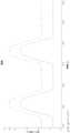
図7は、幾つかの実施形態による、抵抗出力段705を有するRFプラズマリアクタのプラズマシース制御システム700の別の模式図である。この例では、プラズマシース制御システム700はブロッキングダイオードD7を含む。ブロッキングダイオードD7は、正弦波形を整流して、それにより、例えば、図9に示すように、各正弦波形上に平坦な頂部を生成してもよい。ブロッキングダイオードD7は、例えば、正弦波形を整流して、整流各周期の少なくとも10%、15%、20%、25%、30%等の実質的に平坦な部分を有する正弦波形を生成してもよい。 FIG. 7 is another schematic diagram of the plasma
抵抗出力段705は、1つ以上のインダクタL1及び1つ以上の抵抗器R1を含んでもよい。抵抗出力段705は、例えば、「高電圧抵抗出力段回路(HIGH VOLTAGE RESISTIVE OUTPUT STAGE CIRCUIT)」という名称の米国特許出願第15/941,731号に記載されている抵抗出力段のような任意のタイプの抵抗出力段を含んでもよく、同出願は、全ての目的の為にその全体が参照により本開示に組み込まれる。 The
幾つかの実施形態では、抵抗器R1は、約500オーム、約200オーム、約100オーム等未満の抵抗を有してもよい。 In some embodiments, the resistor R1 may have a resistance of less than about 500 ohms, about 200 ohms, about 100 ohms, and the like.
幾つかの実施形態では、抵抗出力段705は、負荷段106(例えば、プラズマチャンバ)及び高電圧スイッチング電源と並列に電気的に結合されていてもよい。幾つかの実施形態では、抵抗出力段は、負荷(例えば、ウェハプラズマシース又は壁プラズマシース510から)を放電する少なくとも1つの抵抗器(例えば、R1)を含んでもよい。幾つかの実施形態では、抵抗出力段は、各正弦波形サイクル中に約1キロワットを超える平均電力及び/又は1ジュール以下のエネルギーを放電するように構成されていてもよい。幾つかの実施形態では、抵抗出力段の抵抗器R1の抵抗は200オーム未満であり得る。幾つかの実施形態では、抵抗器R1は、約200pF未満の結合キャパシタンスを有する直列又は並列に配置された複数の抵抗器(例えば、C11)を含んでもよい。 In some embodiments, the
幾つかの実施形態では、抵抗出力段705は、負荷上の電圧波形の形状を制御する為に使用され得る回路素子の集合体を含んでもよい。幾つかの実施形態では、抵抗出力段705は、受動素子のみ(例えば、抵抗器、コンデンサ、インダクタ等)を含んでもよい。幾つかの実施形態では、抵抗出力段705は、受動回路素子だけでなく能動回路素子(例えば、スイッチ)を含んでもよい。幾つかの実施形態では、抵抗出力段705は、例えば、波形の電圧立上り時間及び/又は波形の電圧立下り時間を制御する為に使用され得る。 In some embodiments, the
幾つかの実施形態では、抵抗出力段705は、容量性負荷(例えば、ウェハプラズマシース505及び/又は壁プラズマシース510からの容量性電荷)を放電することができる。例えば、これらの容量性負荷は小キャパシタンス(例えば、約10pF、100pF、500pF、1nF、10nF、100nF等)を有し得る。 In some embodiments, the
幾つかの実施形態では、抵抗出力段は、高いピーク電圧(例えば、1kV、10kV、20kV、50kV、100kV等を超える電圧)及び/又は高い周波数(例えば、1kHz、10kHz、100kHz、200kHz、500kHz、1MHz等を超える周波数)を有する正弦波形を有する回路で使用され得る。 In some embodiments, the resistance output stage has a high peak voltage (eg, a voltage greater than 1 kV, 10 kV, 20 kV, 50 kV, 100 kV, etc.) and / or a high frequency (eg, 1 kHz, 10 kHz, 100 kHz, 200 kHz, 500 kHz, etc.). It can be used in circuits with sinusoidal waveforms (frequencyes above 1 MHz, etc.).
幾つかの実施形態では、抵抗出力段705は、高い平均電力、高いピーク電力 高速立上り時間及び/又は高速立下り時間を処理するように選択されてもよい。例えば、平均定格電力は、約0.5kW、1.0kW、10kW、25kW等よりも大きくてもよい、及び/又はピーク定格電力は、約1kW、10kW、100kW、1MW等よりも大きくてもよい。 In some embodiments, the
幾つかの実施形態では、抵抗出力段705は、受動コンポーネントの直列又は並列ネットワークを含んでもよい。例えば、抵抗出力段705は、直列の抵抗器R5、コンデンサC11、及びインダクタL7を含んでもよい。別の例として、抵抗出力段705は、インダクタと並列に配置されたコンデンサと、抵抗器と直列に配置されたコンデンサとインダクタの組み合わせを含んでもよい。配置に拘らず、コンポーネント値は、RFソースのRF周波数に一致するように選択されてもよい。ブロッキングダイオードD7はRF発生器515の出力を整流してもよい。例えば、ブロッキングダイオードD7は、正弦波形を整流して、各周期の少なくとも10%、15%、20%、25%、30%等の実質的に平坦な部分を有する正弦波形を作成してもよい。 In some embodiments, the
幾つかの実施形態では、抵抗出力段705は、負荷段106で高電圧容量性負荷(例えば、ウェハプラズマシース505及び/又は壁プラズマシース510からの容量性電荷)を高速放電時間で放電してもよい。高電圧負荷は、約1kV、10kV、20kV、50kV、100kV等よりも大きい電圧を有する負荷であり得る。高速放電時間は、約1ns、10ns、50ns、100ns、250ns、500ns、1000ns等未満の時間であり得る。 In some embodiments, the
プラズマシース制御システム700は、RF発生器515と、抵抗出力段705と、リード段103と、直流バイアス回路104と、第2のリード段105とを含み得る。プラズマシース制御システムは、プラズマシース制御回路と、プラズマチャンバを含み得る負荷段106とを含んでもよい。 The plasma
図8は、回路点122と回路点123との間にあるシースに亘る波形(例えば、コンデンサC3に亘る波形)と、回路点121であるチャックでの波形(例えば、コンデンサC2に亘る波形)とを図示している。図9は、図8に示す波形の3サイクルの拡大図である。波形805は、シースに亘る電圧(例えば、ウェハハプラズマシース505及び/又は壁プラズマシース510からの容量性電荷)を示す。波形805は、ダイオード(D3)故にゼロで僅かにクリップした純正弦波であり、それはプラズマ効果の一部である。波形810は、極での(又はチャックに亘る)電圧を示す。 FIG. 8 shows a waveform over the sheath between the
RFソースV5が連続的にオンされている場合、平坦性は、ブロッキングダイオードD7及び/又は回路内のプラズマシースキャパシタンスを含む全ての関連するキャパシタンスの値の結果であり得る。抵抗出力段705は、RF正弦波の半周期の間にシースキャパシタをリセットしてもよい。波形805は、-2.5kV周辺でより平坦である。波形805の平坦性は、例えば、エッチング中にイオンを一定の電位に保つ為により良くあり得る。抵抗出力段705及び/又はブロッキングダイオードD7は、例えば、この平坦性をもたらし得る。コンポーネント値は、立上り時間、立下り時間、及び/又は出力波形の一部の平坦度を変化させるべく調整されてもよい。 If the RF source V5 is continuously turned on, the flatness may be the result of all relevant capacitance values, including the blocking diode D7 and / or the plasma sheath capacitance in the circuit. The
幾つかの実施形態では、ブロッキングダイオードD7は、例えば高電圧スイッチ等のスイッチで置き換えられてもよい。高電圧スイッチは、図18に示す高電圧スイッチ1800を含んでもよい。高電圧スイッチは、例えば、順方向導通中(例えば、RF発生器515の出力が電圧閾値を超える場合)に閉じ、逆バイアス中(例えば、RF発生器515の出力が電圧閾値未満である場合)に開いてもよい。 In some embodiments, the blocking diode D7 may be replaced with a switch, such as a high voltage switch. The high voltage switch may include the
チャッキング電圧は、バースト時には約500V、オフ時には約2kVとなり得るが、これは許容範囲内である。RF出力電圧を約4kVまで上げると、図10に示すように、オン時とオフ時の両方で差は約2kVになり得る。RF出力電圧を6kV程度まで上げると、図11に示すように、オン時の差が3kV以上になり得るが、それは許容され得ず、又、オフ時には2kV程度の差が生じ得る。3kVの差があると、ウェハが損傷する可能性がある。 The chucking voltage can be about 500V at burst and about 2kV at off, which is acceptable. When the RF output voltage is increased to about 4 kV, the difference can be about 2 kV both on and off, as shown in FIG. When the RF output voltage is increased to about 6 kV, as shown in FIG. 11, the difference at on time can be 3 kV or more, but this is unacceptable, and the difference at off time can be about 2 kV. A difference of 3 kV can damage the wafer.
図12は、幾つかの実施形態による、抵抗出力段705及び直流バイアス回路1204を有するRFプラズマリアクタのプラズマシース制御システム1200の別の模式図である。 FIG. 12 is another schematic diagram of a plasma
直流バイアス回路1204は、直流バイアス回路104に示されたコンポーネントを含み得る。直流バイアス回路1204は、高電圧スイッチS1及び/又はブロッキングダイオードD2をも含み得る。幾つかの実施形態では、高電圧スイッチS1は、高電圧を包括的に開閉する為に直列に配置された複数のスイッチを含んでもよい。高電圧スイッチS1は、例えば、図18に示す高電圧スイッチ1800等の高電圧スイッチを含み得る。
幾つかの実施形態では、高電圧スイッチS1は、RF電源V5の電圧波形が正の場合に開き、負の場合に閉じていてもよい。閉じている間、高電圧スイッチS1は、例えば、ブロッキングダイオードD2に亘る電流を短絡してもよい。この電流を短絡することにより、ウェハとチャックとの間のバイアスが約2kVに維持され得るがこれは許容範囲内であり得る、及び/又は直流バイアス供給電圧V1を変更することにより調整されてもよい。 In some embodiments, the high voltage switch S1 may be open when the voltage waveform of the RF power supply V5 is positive and closed when the voltage waveform of the RF power supply V5 is negative. While closed, the high voltage switch S1 may short-circuit the current across the blocking diode D2, for example. By shorting this current, the bias between the wafer and the chuck can be maintained at about 2 kV, which can be acceptable and / or even if adjusted by changing the DC bias supply voltage V1. good.
図13は、図12の回路からのシースに亘る(例えば、C3)波形及びチャックでの(例えば、C2)波形を示す。図示のように、ウェハとチャッキング電圧の差は、RF電源がオンであるかオフであるかに拘らず、-2kVに非常に近い状態を維持している。 FIG. 13 shows a waveform across the sheath (eg, C3) from the circuit of FIG. 12 and a waveform on the chuck (eg, C2). As shown, the difference between the wafer and the chucking voltage remains very close to -2kV regardless of whether the RF power supply is on or off.
図14は、図12に示した波形の3サイクルの拡大図である。 FIG. 14 is an enlarged view of three cycles of the waveform shown in FIG.
図15は、チャック上の電圧がゼロに戻るバースト波形の終盤部分を示す。 FIG. 15 shows the final part of the burst waveform in which the voltage on the chuck returns to zero.
図16は、幾つかの実施形態によるプラズマシース制御システム1600の回路図である。この例では、プラズマシース制御システム1600は、フルブリッジドライバ1605を含んでもよい。フルブリッジドライバ1605は、直流電圧源(例えば、容量性電源、交流/直流コンバータ等)であり得る入力電圧源V1を含み得る。幾つかの実施形態では、フルブリッジドライバ1605は4個のスイッチを含んでもよい。幾つかの実施形態では、ドライバは、直列又は並列に配置された複数のスイッチを含んでもよい。これらのスイッチは、例えば、例えばIGBT、MOSFET、SiC MOSFET、SiC接合トランジスタ、FET、SiCスイッチ、GaNスイッチ、光導電性スイッチ等の任意のタイプのソリッドステートスイッチを含んでもよい。これらのスイッチは高周波数でスイッチングされてもよく、及び/又は高電圧の正弦波形を生成してもよい。これらの周波数は、例えば、約400kHz、0.5MHz、2.0MHz、4.0MHz、13.56MHz、27.12MHz、40.68MHz、50MHz等の周波数を含んでもよい。 FIG. 16 is a circuit diagram of the plasma
幾つかの実施形態では、フルブリッジドライバは共振回路1610と結合される。共振回路1610は、トランスT1に結合された共振インダクタL5及び/又は共振コンデンサC2を含んでもよい。幾つかの実施形態では、トランスT1は取り除かれてもよい。共振回路は、例えば、フルブリッジドライバと共振回路1610との間の任意のリード線の抵抗、及び/又は共振回路1610内の任意のコンポーネント、例えば、トランスT1、コンデンサC2、インダクタL5、及び抵抗器R5を含む漂遊抵抗R5をも含み得る。 In some embodiments, the full bridge driver is coupled with a
他の回路要素のインダクタンス及び/又はキャパシタンスは駆動周波数に影響を与え得るが、駆動周波数は概ね、共振インダクタL5及び/又は共振コンデンサC2の選択によって設定され得る。適切な駆動周波数を作成する為に、更なる改良及び/又はチューニングが必要となり得る。更に、トランスT1に亘る立上り時間は、以下の条件で、インダクタL5のインダクタンス及び/又はコンデンサC2のキャパシタンスを変更することによって調整され得る。
例えば、コンデンサC2、抵抗器R5、又はインダクタL5は、他の要素が経時変化しても周波数が一定であることを確実にする為に、デバイスの値を調整又は変更できるように、調整可能であってもよい。 For example, the capacitor C2, resistor R5, or inductor L5 can be adjusted so that the value of the device can be adjusted or changed to ensure that the frequency remains constant over time for other elements. There may be.
幾つかの実施形態では、インダクタL5のインダクタンス値が大きいと、立上り時間が遅くなるか、又は短くなることがある。これらの値はバーストエンベロープにも影響を与え得る。各バーストは過渡状態及び定常状態の正弦波形を含み得る。各バースト内の過渡正弦波形は、定常正弦波形の間に完全な電圧に達するまで、L5及び/又はシステムのQによって設定される。 In some embodiments, a large inductance value of the inductor L5 may slow or shorten the rise time. These values can also affect the burst envelope. Each burst may contain transient and steady state sinusoidal waveforms. The transient sinusoidal waveform within each burst is set by L5 and / or the Q of the system until the full voltage is reached during the steady sinusoidal waveform.
ドライバ回路内のスイッチが共振周波数fresonantで切り替えられると、トランスでの出力電圧は増幅される。幾つかの実施形態では、共振周波数は、約20Hz、50Hz、100Hz、250Hz、400kHz、0.5MHz、2.0MHz、4.0MHz、13.56MHz、27.12MHz、40.68MHz、50MHz、100MHz等であり得る。When the switch in the driver circuit is switched at the resonance frequencyfresonant , the output voltage in the transformer is amplified. In some embodiments, the resonant frequencies are about 20 Hz, 50 Hz, 100 Hz, 250 Hz, 400 kHz, 0.5 MHz, 2.0 MHz, 4.0 MHz, 13.56 MHz, 27.12 MHz, 40.68 MHz, 50 MHz, 100 MHz, etc. Can be.
幾つかの実施形態では、共振コンデンサC2は、トランスT1の漂遊キャパシタンス及び/又は物理的コンデンサを含んでもよい。幾つかの実施形態では、共振コンデンサC2は、約10μF、約1μF、約100nF、約10nF等のキャパシタンスを有してもよい。幾つかの実施形態では、共振インダクタL5は、トランスT1の漂遊インダクタンス及び/又は物理的インダクタを含んでもよい。幾つかの実施形態では、共振インダクタL5は、約50nH、約100nH、約150nH、約500nH、約1000nH等のインダクタンスを有してもよい。幾つかの実施形態では、共振抵抗器R5は、約10オーム、約25オーム、約50オーム、約100オーム、約150オーム、約500オーム等の抵抗を有してもよい。 In some embodiments, the resonant capacitor C2 may include a stray capacitance and / or a physical capacitor of the transformer T1. In some embodiments, the resonant capacitor C2 may have a capacitance of about 10 μF, about 1 μF, about 100 nF, about 10 nF, and the like. In some embodiments, the resonant inductor L5 may include a stray inductance of the transformer T1 and / or a physical inductor. In some embodiments, the resonant inductor L5 may have an inductance of about 50 nH, about 100 nH, about 150 nH, about 500 nH, about 1000 nH, and the like. In some embodiments, the resonant resistor R5 may have a resistance of about 10 ohms, about 25 ohms, about 50 ohms, about 100 ohms, about 150 ohms, about 500 ohms, and the like.
幾つかの実施形態では、プラズマチャンバ内のプラズマ負荷は、時間変動する負荷であり得る。この時間変動は、共振回路のインダクタンス又はキャパシタンスの何れか又は両方に影響を与え、共振周波数fresonantのシフトを引き起こす可能性がある。幾つかの実施形態では、プラズマシース制御システムは、コントローラ(例えば、マイクロコントローラ、FPGA、又は任意の制御装置)を含んでもよい。幾つかの実施形態では、このコントローラは、例えば点121において、プラズマシース制御システムの出力電圧及び/又は電流を測定してもよい。幾つかの実施形態では、この電圧又は電流の測定は、プラズマシース制御システムが共振周波数で動作しているかどうかを判断する為に使用されてもよい。幾つかの実施形態では、システムが共振周波数で動作していない場合、制御装置は、例えば、共振回路1610におけるインダクタンス又はキャパシタンスの値を調整することによって、プラズマシース制御システムの動作周波数を共振周波数に一致するように変更してもよい。In some embodiments, the plasma load in the plasma chamber can be a time-varying load. This time variation affects either or both of the inductance and capacitance of the resonant circuit and can cause a shift in the resonant frequencyfresonant . In some embodiments, the plasma sheath control system may include a controller (eg, a microcontroller, FPGA, or any control device). In some embodiments, the controller may measure the output voltage and / or current of the plasma sheath control system, eg, at
幾つかの実施形態では、例えば点121、122、124、125、又は回路内の任意の点でプラズマシース制御システムによって生成される電流又は電圧波形の振幅が、コントローラによって測定されてもよい。幾つかの実施形態では、測定された電流及び/又は電圧を使用して、プラズマシース制御システムの出力電力を決定してもよい。幾つかの実施形態では、コントローラは、この測定に応答して、動作周波数、電圧、又はデューティサイクルを変更することで、所望の出力電圧、電流、又は電力レベルを達成してもよい。 In some embodiments, the amplitude of the current or voltage waveform generated by the plasma sheath control system may be measured by the controller, for example at
幾つかの実施形態では、プラズマシース制御システムの動作周波数及び出力電力の何れか又は両方がコントローラによって制御されてもよい。幾つかの実施形態では、コントローラは、出力波形の変動を検出して、例えば、約100ms未満、約1ms未満、約10μs未満、約500ns未満等の高速タイムスケールで動作周波数及び/又は電力レベルを調整してもよい。 In some embodiments, either or both of the operating frequency and output power of the plasma sheath control system may be controlled by the controller. In some embodiments, the controller detects variations in the output waveform and sets the operating frequency and / or power level on a high speed timescale, eg, less than about 100 ms, less than about 1 ms, less than about 10 μs, less than about 500 ns, and so on. You may adjust it.
幾つかの実施形態では、抵抗器R5は、物理的回路内のワイヤ、トレース、及び/又はトランス巻線の漂遊抵抗を表し得る。幾つかの実施形態では、抵抗器R5は、約10オーム、約50オーム、約100オーム、約200オーム、約500オーム等の抵抗を有してもよい。 In some embodiments, the resistor R5 may represent drift resistance of wires, traces, and / or transformer windings in a physical circuit. In some embodiments, the resistor R5 may have a resistance of about 10 ohms, about 50 ohms, about 100 ohms, about 200 ohms, about 500 ohms, and the like.
幾つかの実施形態では、トランスT1は、「高電圧トランス(High Voltage Transformer)」という名称の米国特許出願第15/365,094号に開示されているようなトランスを含んでもよく、同出願は、全ての目的の為に本明細書に組み込まれる。 In some embodiments, the transformer T1 may include a transformer as disclosed in US Patent Application No. 15 / 365,094 entitled "High Voltage Transformer", which application. , Incorporated herein for all purposes.
幾つかの実施形態では、共振回路1610の出力電圧は、スイッチS1、S2、S3、及び/又はS4のデューティサイクル(例えば、スイッチ「オン」時間、又はスイッチが導通している時間)を変更することによって変更され得る。例えば、デューティサイクルが長いほど出力電圧は高くなり、デューティサイクルが短いほど出力電圧は短くなる。幾つかの実施形態では、共振回路1610の出力電圧は、フルブリッジドライバにおけるスイッチングのデューティサイクルを調整することによって変更又は調整され得る。例えば、スイッチS1、S2、S3、S4を開閉する、信号、例えばSig1及びSig2のデューティサイクルを調整することによって、駆動装置の出力電圧が調整され得る。 In some embodiments, the output voltage of the
幾つかの実施形態では、共振回路の各スイッチ(例えば、S1、S2、S3、及び/又はS4)は、独立して、又は他のスイッチのうちの1つ以上のスイッチと連動して切り替えられ得る。 In some embodiments, each switch in the resonant circuit (eg, S1, S2, S3, and / or S4) is switched independently or in conjunction with one or more of the other switches. obtain.
幾つかの実施形態では、共振回路1610は、半波整流器1615及び/又はブロッキングダイオードD7と結合されてもよい。幾つかの実施形態では、ブロッキングダイオードD7は、例えば高電圧スイッチのようなスイッチで置き換えられてもよい。高電圧スイッチは、図18に示す高電圧スイッチ1800を含んでもよい。高電圧スイッチは、例えば、順方向導通中(例えば、RF発生器515の出力が電圧閾値を超えているとき)に閉じ、逆バイアス中(例えば、RF発生器515の出力が電圧閾値を下回っているとき)に開いていてもよい。 In some embodiments, the
幾つかの実施形態では、ブロッキングダイオードD7は、フルブリッジドライバ1605からの正弦波形を整流してもよい。例えば、ブロッキングダイオードD7は、正弦波形を整流して、各周期の少なくとも10%、15%、20%、25%、30%等の実質的に平坦な部分を有する整流された正弦波形を作成してもよい。 In some embodiments, the blocking diode D7 may rectify a sinusoidal waveform from the
幾つかの実施形態では、半波整流器1615又はブロッキングダイオードD7は抵抗出力段1620に結合されてもよい。抵抗出力段1620は、当該技術分野で知られている任意の抵抗出力段を含んでもよい。例えば、抵抗出力段1620は、「高電圧抵抗出力段回路(HIGH VOLTAGE RESISTIVE OUTPUT STAGE CIRCUIT)」という名称の米国特許出願第16/178,538号に記載されている任意の抵抗出力段を含んでもよく、同出願は、全ての目的の為にその全体が本開示に組み込まれる。例えば、抵抗出力段1620は抵抗出力段705内の要素を含んでもよい。 In some embodiments, the half-
幾つかの実施形態では、抵抗出力段は、負荷(例えば、プラズマシースキャパシタンス)を放電する少なくとも1つの抵抗器(例えば、R1)を含んでもよい。幾つかの実施形態では、抵抗出力段は、各正弦波形サイクル中に約1キロワットを超える平均電力及び/又は1ジュール以下のエネルギーを放電するように構成されてもよい。幾つかの実施形態では、抵抗出力段の抵抗器R1の抵抗は200オーム未満であってもよい。幾つかの実施形態では、抵抗器R1は、約200pF未満の結合キャパシタンスを有する直列又は並列に配置された複数の抵抗器を含んでもよい(例えば、C11)。 In some embodiments, the resistance output stage may include at least one resistor (eg, R1) that discharges the load (eg, plasma sheath capacitance). In some embodiments, the resistance output stage may be configured to discharge an average power of greater than about 1 kW and / or less than 1 joule of energy during each sinusoidal cycle. In some embodiments, the resistance of the resistor R1 in the resistance output stage may be less than 200 ohms. In some embodiments, the resistor R1 may include a plurality of resistors arranged in series or in parallel with a coupling capacitance of less than about 200 pF (eg, C11).
幾つかの実施形態では、抵抗出力段1620は、負荷上の電圧波形の形状を制御する為に使用され得る回路素子の集合体を含んでもよい。幾つかの実施形態では、抵抗出力段1620は、受動素子のみ(例えば、抵抗器、コンデンサ、インダクタ等)を含んでもよい。幾つかの実施形態では、抵抗出力段1620は、受動回路素子だけでなく、能動回路素子(例えば、スイッチ)を含んでもよい。幾つかの実施形態では、抵抗出力段1620は、例えば、波形の電圧立上り時間及び/又は波形の電圧立下り時間を制御する為に使用され得る。 In some embodiments, the
幾つかの実施形態では、抵抗出力段1620は、容量性負荷(例えば、ウェハプラズマシース505及び/又は壁プラズマシース510からの容量性電荷)を放電することができる。例えば、これらの容量性負荷は、小キャパシタンス(例えば、約10pF、100pF、500pF、1nF、10nF、100nF等)を有してもよい。 In some embodiments, the
幾つかの実施形態では、抵抗出力段1620は、高いピーク電圧(例えば、1kV、10kV、20kV、50kV、100kV等を超える電圧)及び/又は高い周波数(例えば、1kHz、10kHz、100kHz、200kHz、500kHz、1MHz等を超える周波数)及び/又は約400kHz、0.5MHz、2.0MHz、4.0MHz、13.56MHz、27.12MHz、40.68MHz、50MHz等の周波数を有する正弦波形を有する回路で使用され得る。 In some embodiments, the
幾つかの実施形態では、抵抗出力段1620は、高平均電力、高ピーク電力、高速立上り時間及び/又は高速立下り時間を処理するように選択されてもよい。例えば、平均定格電力は、約0.5kW、1.0kW、10kW、25kW等を超えていてもよいし、及び/又はピーク定格電力は、約1kW、10kW、100kW、1MW等を超えていてもよい。 In some embodiments, the
幾つかの実施形態では、抵抗出力段1620は、受動コンポーネントの直列又は並列ネットワークを含んでもよい。例えば、抵抗出力段1620は、直列の抵抗器、コンデンサ、及びインダクタを含んでもよい。別の例として、抵抗出力段1620は、インダクタと並列にコンデンサを含んでもよく、抵抗器と直列のコンデンサとインダクタの組み合わせを含んでもよい。例えば、L11は、整流器から出る電圧がある場合に抵抗出力段に有意なエネルギーが注入されないように、十分に大きく選択され得る。R3とR1の値は、L/R時間がRF周波数よりも高速で負荷の適切なコンデンサをドレインするように選択され得る。 In some embodiments, the
幾つかの実施形態では、抵抗出力段1620はバイアス補償回路1625に結合されてもよい。 In some embodiments, the
バイアス補償回路1625は、当該技術分野で知られている任意のバイアス及び/又はバイアス補償回路を含んでもよい。例えば、バイアス補償回路1625は、「ナノ秒パルサーバイアス補償(NANOSECOND PULSER BIAS COMPENSATION)」という名称の米国特許出願第162/711,406号に記載されている任意のバイアス及び/又はバイアス補償回路を含んでもよく、同出願は、全ての目的の為に本開示に組み込まれる。 The
幾つかの実施形態では、バイアス補償回路1625は、バイアスコンデンサC7、ブロッキングコンデンサC12、ブロッキングダイオードD8、スイッチS8(例えば、高電圧スイッチ)、オフセット供給電圧V1、抵抗R2、及び/又は抵抗R4を含んでもよい。幾つかの実施形態では、スイッチS8は、例えば、図18に示す高電圧スイッチ1800等の高電圧スイッチを含む。 In some embodiments, the
幾つかの実施形態では、オフセット供給電圧V5は、出力電圧を正又は負の何れかにバイアスすることができる直流電圧源を含んでもよい。幾つかの実施形態では、コンデンサC12は、オフセット供給電圧V5を抵抗出力段1620及び/又は他の回路要素から絶縁/分離してもよい。幾つかの実施形態では、バイアス補償回路1625は、回路の或る部分から別の部分への電位シフトを可能にしてもよい。幾つかの実施形態では、バイアス補償回路1625は、高電圧正弦波形がチャンバ内で活性化されているとき、ウェハを所定の位置に保持する為に使用されてもよい。抵抗R2は、ブリッジドライバからの直流バイアス供給を保護/絶縁してもよい。 In some embodiments, the offset supply voltage V5 may include a DC voltage source capable of biasing the output voltage to either positive or negative. In some embodiments, the capacitor C12 may insulate / separate the offset supply voltage V5 from the
幾つかの実施形態では、スイッチS8は、フルブリッジドライバ1605がパルシングしている間は開き、フルブリッジドライバ1605がパルシングしていないときは閉じていてもよい。閉じている間、スイッチS8は、例えば、ブロッキングダイオードD8に亘る電流を短絡してもよい。この電流を短絡することにより、ウェハとチャックとの間のバイアスが2kV未満となるがこれは許容範囲内であり得る。 In some embodiments, the switch S8 may be open while the
幾つかの実施形態では、プラズマシース制御システム1600は、例えば、50オームのマッチングネットワーク又は外部マッチングネットワーク又はスタンドアロンマッチングネットワーク等の従来のマッチングネットワークを含んでも、含まなくてもよい。本明細書に記載された実施形態は、ウェハチャンバに印加されるスイッチング電力をチューニングする為に、50オームのマッチングネットワークを必要としても、必要としなくてもよい。典型的には、マッチングネットワークのチューニングには、少なくとも100μs~200μsかかり得る。幾つかの実施形態では、電力変化は、1又は2RFサイクル内、例えば、400kHzで2.5μs~5.0μsで起こり得る。 In some embodiments, the plasma
図17は、幾つかの実施形態によるプラズマシース制御システム1700の回路図である。プラズマシース制御システム1700は、例えばプラズマチャンバを駆動する為等の高電圧及び高周波数正弦波形を生成する波形発生器1745を含む。幾つかの実施形態では、波形発生器1745は、1kV、10kV、20kV、50kV、100kV等を超えるピーク電圧と、1kHz、10kHz、100kHz、200kHz、500kHz、1MHz等を超える高周波数とを有する正弦波形を発生する任意の装置を含んでもよい。 FIG. 17 is a circuit diagram of the plasma
幾つかの実施形態では、波形発生器1745は、RF発生器515、フルブリッジドライバ1605、又はハーフブリッジドライバ1905を含んでもよい。幾つかの実施形態では、波形発生器1745はトランスを含んでも、含まなくてもよい。 In some embodiments, the
幾つかの実施形態では、波形発生器1745はエネルギー回収回路1705と結合してもよい。波形発生器1745がトランスを含む場合、エネルギー回収回路1705はトランスT1の二次側に配置されてもよいし、又はトランスT1の二次側に電気的に結合されてもよい。 In some embodiments, the
エネルギー回収回路1705は、例えば、トランスT1の二次側に亘るダイオード1730(例えば、クローバーダイオード)を含んでもよい。エネルギー回収回路1705は、例えば、ダイオード1710及びインダクタ1715(直列に配置されている)を含んでもよく、これにより、負荷段106(例えば、容量性負荷)の放電から電流を流して電源C7を充電することができる。ダイオード1710及びインダクタ1715は、負荷段106及び電源C7と電気的に接続されていてもよい。 The
幾つかの実施形態では、エネルギー回収回路1705はブロッキングダイオード1735を含んでもよい。ブロッキングダイオード1735は、ブロッキングダイオードD7に類似していてもよいし、ブロッキングダイオードD7に類似した方式で動作してもよい。例えば、ブロッキングダイオード1735は、正弦波形を整流してもよく、これは、例えば、各正弦波形上に平坦な頂部を生成してもよい(例えば、図9に示すように)。例えば、ブロッキングダイオード1735は、正弦波形を整流して、各周期の少なくとも10%、15%、20%、25%、30%等に実質的に平坦な部分を有する正弦波形を生成してもよい。 In some embodiments, the
幾つかの実施形態では、ブロッキングダイオード1735は、例えば、高電圧スイッチ等のスイッチで置き換えられてもよい。高電圧スイッチは、図18に示す高電圧スイッチ1800を含んでもよい。高電圧スイッチは、例えば、順方向導通中(例えば、RF発生器515の出力が電圧閾値を超えている場合)に閉じられ、逆バイアス中(例えば、RF発生器515の出力が電圧閾値を下回っている場合)に開いていてもよい。 In some embodiments, the blocking
幾つかの実施形態では、エネルギー回収回路1705は、負荷段106と電気的に結合されたインダクタ1740を含んでもよい。インダクタ1740は、波形発生器1745内のトランスの漂遊インダクタンスを表し得る、及び/又は、波形発生器1745とエネルギー回収回路1705との間の漂遊インダクタンス(例えば、インダクタンストランスT1)を含み得る。 In some embodiments, the
波形発生器1745がオンにされると、電流が負荷段106を充電し得る(例えば、コンデンサC3、コンデンサC2、又はコンデンサC9を充電し得る)。一部の電流は、例えば、トランスT1の二次側の電圧が電源C7の充電電圧より上に上昇したときに、インダクタ1715を通って流れ得る。波形発生器1745がオフになると、電流は、負荷段106内のコンデンサからインダクタ1715を通って流れてインダクタ1715に亘る電圧がゼロになるまで電源C7を充電してもよい。ダイオード1730は、負荷段106内のコンデンサが、負荷段106内のインダクタンス又は直流バイアス回路104のインダクタンスによってリンギングするのを防止してもよい。 When the
ダイオード1710は、例えば、電源C7から負荷段106内のコンデンサに電荷が流れるのを防止し得る。 The
インダクタ1715の値は、電流立下り時間を制御するように選択されてもよい。幾つかの実施形態では、インダクタ1715は、1μH~500μHのインダクタンス値を有し得る。 The value of the
幾つかの実施形態では、エネルギー回収回路1705は、インダクタ1715を通る電流の流れを制御する為に使用され得るスイッチを含んでもよい。スイッチは、例えば、インダクタ1715と直列に配置されてもよい。幾つかの実施形態では、スイッチは、スイッチS1が開いているとき及び/又はもはやパルシングしていないときに閉じて、負荷段106から高電圧負荷C7に戻る電流の流れを可能にしてもよい。スイッチは、例えば、高電圧スイッチ1800等の高電圧スイッチを含んでもよい。 In some embodiments, the
エネルギー回収回路1705は、プラズマシース制御システム500、プラズマシース制御システム700、プラズマシース制御システム1200、プラズマシース制御システム1600、又はプラズマシース制御システム1900に追加されてもよい。幾つかの実施形態では、エネルギー回収回路1705は、例えば、抵抗出力段705又は抵抗出力段1620等の抵抗出力段を置き換えてもよい。 The
直流バイアス回路1704は、直流バイアス回路1704、バイアス補償回路1625、直流バイアス回路1204、又は直流バイアス回路104を含んでもよい。 The
第2のリード段105は、波形発生器1745と負荷段106との間の回路素子を表してもよい。 The second
この例では、プラズマシース制御システム1700は、負荷段106と結合され、正弦波形を負荷段106に提供してもよく、負荷段106は、例えば、負荷段106の任意の要素を含み得る。 In this example, the plasma
図18は、幾つかの実施形態による絶縁された電力を有する高電圧スイッチ1800のブロック図である。高電圧スイッチ1800は、高速立上り時間及び/又は高周波数及び/又は可変周期を有する高電圧源1860からの電圧を切り替え得る複数のスイッチモジュール1805(集合的に又は個別に1805、及び個別に1805A、1805B、1805C及び1805D)を含んでもよい。各スイッチモジュール1805は、例えばソリッドステートスイッチ等のスイッチ1810を含んでもよい。 FIG. 18 is a block diagram of a
幾つかの実施形態では、スイッチ1810は、電源1840(例えば、1840A、1840B、1840C又は1840D)及び/又は絶縁ファイバトリガ1845(例えば、1845A、1845B、1845C、又は1845D)(ゲートトリガ又はスイッチトリガとも呼ばれる)を含み得るゲートドライバ回路1830と電気的に結合されてもよい。例えば、スイッチ1810は、コレクタ、エミッタ及びゲート(又はドレイン、ソース、及びゲート)を含んでもよく、電源1840は、ゲートドライバ回路1830を介してスイッチ1810のゲートを駆動してもよい。ゲートドライバ回路1830は、例えば、高電圧スイッチ1800の他のコンポーネントから絶縁されていてもよい。 In some embodiments, the switch 1810 is a power supply 1840 (eg, 1840A, 1840B, 1840C or 1840D) and / or an isolated fiber trigger 1845 (eg, 1845A, 1845B, 1845C, or 1845D) (also a gate trigger or switch trigger). It may be electrically coupled to a gate driver circuit 1830 which may include (called). For example, switch 1810 may include collectors, emitters and gates (or drains, sources, and gates), and power supply 1840 may drive the gates of switch 1810 via a gate driver circuit 1830. The gate driver circuit 1830 may be isolated from other components of the
幾つかの実施形態では、電源1840は、例えば、絶縁トランスを使用して絶縁されてもよい。絶縁トランスは低キャパシタンストランスを含んでもよい。絶縁トランスの低キャパシタンスは、例えば、電源1840が、有意な電流を要さずに高速の時間スケールで充電することを可能にし得る。絶縁トランスは、例えば約100pF未満のキャパシタンスを有してもよい。別の例として、絶縁トランスは、約30未満から100pFのキャパシタンスを有してもよい。幾つかの実施形態では、絶縁トランスは、1kV、5kV、10kV、25kV、50kV等までの電圧絶縁を提供してもよい。 In some embodiments, the power supply 1840 may be isolated using, for example, an isolation transformer. The isolation transformer may include a low capacitance transformer. The low capacitance of the isolation transformer may allow, for example, the power supply 1840 to charge at a high speed time scale without the need for significant current. The isolation transformer may have a capacitance of less than, for example, about 100 pF. As another example, the isolation transformer may have a capacitance of less than about 30 to 100 pF. In some embodiments, the isolation transformer may provide voltage isolation up to 1 kV, 5 kV, 10 kV, 25 kV, 50 kV, and the like.
幾つかの実施形態では、絶縁トランスは、低い漂遊キャパシタンスを有してもよい。例えば、絶縁トランスは、約1000pF、100pF、10pF等よりも小さい漂遊キャパシタンスを有してもよい。幾つかの実施形態では、低キャパシタンスは、低電圧コンポーネント(例えば、入力制御電力の源)への電気的結合を最小化、及び/又はEMI発生(例えば、電気的ノイズ発生)を低減し得る。幾つかの実施形態では、絶縁トランスのトランス漂遊キャパシタンスは、一次巻線と二次巻線との間で測定されたキャパシタンスを含み得る。 In some embodiments, the isolation transformer may have a low stray capacitance. For example, the isolation transformer may have a stray capacitance smaller than about 1000pF, 100pF, 10pF and the like. In some embodiments, the low capacitance may minimize electrical coupling to low voltage components (eg, sources of input control power) and / or reduce EMI generation (eg, electrical noise generation). In some embodiments, the transformer stray capacitance of an isolation transformer may include the capacitance measured between the primary and secondary windings.
幾つかの実施形態では、絶縁トランスは、直流/直流コンバータ又は交流/直流トランスであってもよい。幾つかの実施形態では、トランスは、例えば、110Vの交流トランスを含んでもよい。それにも拘らず、絶縁トランスは、高電圧スイッチ1800内の他のコンポーネントから絶縁されたパワーを供給できる。幾つかの実施形態では、絶縁はガルバニックであり、絶縁トランスの一次側の導体が絶縁トランスの二次側の導体を通過しないように、又は絶縁トランスの二次側の導体と接触しないようになっていてもよい。 In some embodiments, the isolation transformer may be a DC / DC converter or an AC / DC transformer. In some embodiments, the transformer may include, for example, a 110V AC transformer. Nevertheless, the isolation transformer can supply isolated power from other components within the
幾つかの実施形態では、絶縁トランスは、トランスコアに緊密に巻かれるかトランスコアを包囲し得る一次巻線を含んでいてもよい。幾つかの実施形態では、一次巻線は、トランスコアの周りを包囲する導電性シートを含んでもよい。幾つかの実施形態では、一次巻線は、1つ以上の巻線を含んでもよい。 In some embodiments, the isolation transformer may include a primary winding that may be tightly wound around the transformer core or may surround the transformer core. In some embodiments, the primary winding may include a conductive sheet that surrounds the transcore. In some embodiments, the primary winding may include one or more windings.
幾つかの実施形態では、二次巻線は、可能な限りコアから離れてコアの周りに巻かれてもよい。例えば、二次巻線を含む巻線の束は、トランスコアの開口部の中心を通って巻かれてもよい。幾つかの実施形態では、二次巻線は1つ以上の巻線を含んでもよい。幾つかの実施形態では、二次巻線を含む巻線の束は、漂遊キャパシタンスを最小化する為に、例えば円形又は正方形である断面を含んでもよい。幾つかの実施形態では、絶縁体(例えば、油又は空気)が、一次巻線、二次巻線、又はトランスコアの間に配置されてもよい。 In some embodiments, the secondary winding may be wound around the core as far as possible from the core. For example, a bundle of windings, including a secondary winding, may be wound through the center of the opening in the transcore. In some embodiments, the secondary winding may include one or more windings. In some embodiments, the bundle of windings, including the secondary winding, may include, for example, a circular or square cross section to minimize stray capacitance. In some embodiments, an insulator (eg, oil or air) may be placed between the primary winding, the secondary winding, or the transcore.
幾つかの実施形態では、二次巻線をトランスコアから離しておくことには幾つかの利点があり得る。例えば、離すことで、絶縁トランスの一次側と絶縁トランスの二次側との間の漂遊キャパシタンスを減少させる可能性がある。別の例として、離すことで、絶縁トランスの一次側と絶縁トランスの二次側との間の高電圧のスタンドオフを可能にし、動作中にコロナ及び/又は絶縁破壊が形成されないようにすることができる可能性がある。 In some embodiments, keeping the secondary winding away from the transcore may have several advantages. For example, separating them may reduce the stray capacitance between the primary side of the isolation transformer and the secondary side of the isolation transformer. As another example, separating allows high voltage standoff between the primary side of the isolation transformer and the secondary side of the isolation transformer to prevent corona and / or dielectric breakdown during operation. May be possible.
幾つかの実施形態では、絶縁トランスの一次側(例えば、一次巻線)と絶縁トランスの二次側(例えば、二次巻線)との間の間隔は、約0.1インチ、約0.5インチ、約1インチ、約5インチ、又は約10インチであり得る。幾つかの実施形態では、絶縁トランスのコアと絶縁トランスの二次側(例えば、二次巻線)との間の典型的な間隔は、約0.1インチ、0.5インチ、1インチ、5インチ又は10インチであり得る。幾つかの実施形態では、巻線間のギャップは、例えば、真空、空気、任意の絶縁性ガス又は液体、又は比誘電率が3未満の固体材料等の、誘電率が可能な限り低い誘電体材料で満たされてもよい。 In some embodiments, the distance between the primary side of the isolation transformer (eg, the primary winding) and the secondary side of the isolation transformer (eg, the secondary winding) is about 0.1 inch, about 0. It can be 5 inches, about 1 inch, about 5 inches, or about 10 inches. In some embodiments, the typical spacing between the core of the isolation transformer and the secondary side of the isolation transformer (eg, the secondary winding) is about 0.1 inch, 0.5 inch, 1 inch, It can be 5 inches or 10 inches. In some embodiments, the gap between the windings is a dielectric with the lowest possible dielectric constant, such as vacuum, air, any insulating gas or liquid, or a solid material with a relative permittivity of less than 3. It may be filled with material.
幾つかの実施形態では、電源1840は、高電圧スタンドオフ(絶縁)を提供することができるか、又は低キャパシタンス(例えば、約1,000pF未満、100pF未満、10pF未満等)を有し得る任意のタイプの電源を含んでもよい。幾つかの実施形態では、制御電圧電源は、60Hzで交流1820V又は交流240Vを供給してもよい。 In some embodiments, the power supply 1840 can provide high voltage standoff (insulation) or can have low capacitance (eg, less than about 1,000 pF, less than 100 pF, less than 10 pF, etc.). Type of power supply may be included. In some embodiments, the control voltage power supply may supply AC 1820V or AC 240V at 60Hz.
幾つかの実施形態では、各電源1840は、単一の制御電圧電源と誘導的に電気的に結合されてもよい。例えば、電源1840Aは第1のトランスを介して電源と電気的に結合されてもよく、電源1840Bは第2のトランスを介して電源と電気的に結合されてもよく、電源1840Cは第3のトランスを介して電源と電気的に結合されてもよく、電源1840Dは第4のトランスを介して電源と電気的に結合されてもよい。例えば、様々な電源間の電圧絶縁を提供することができる任意のタイプのトランスが使用されてもよい。 In some embodiments, each power source 1840 may be inductively electrically coupled to a single control voltage power source. For example, the
幾つかの実施形態では、第1のトランス、第2のトランス、第3のトランス及び第4のトランスは、単一のトランスのコアの周りに異なる二次巻線を含んでもよい。例えば、第1のトランスは第1の二次巻線を含んでもよく、第2のトランスは第2の二次巻線を含んでもよく、第3のトランスは第3の二次巻線を含んでもよく、第4のトランスは第4の二次巻線を含んでもよい。これらの各二次巻線は単一のトランスのコアに巻かれていてもよい。幾つかの実施形態では、第1の二次巻線、第2の二次巻線、第3の二次巻線、第4の二次巻線、又は一次巻線は、トランスコアの周りに巻かれた単一の巻線又は複数の巻線を含んでもよい。 In some embodiments, the first transformer, the second transformer, the third transformer and the fourth transformer may include different secondary windings around the core of a single transformer. For example, the first transformer may include a first secondary winding, the second transformer may include a second secondary winding, and the third transformer may include a third secondary winding. However, the fourth transformer may include a fourth secondary winding. Each of these secondary windings may be wound around the core of a single transformer. In some embodiments, the first secondary winding, the second secondary winding, the third secondary winding, the fourth secondary winding, or the primary winding is around the transformer core. It may include a single wound winding or a plurality of windings.
幾つかの実施形態では、電源1840A、電源1840B、電源1840C及び/又は電源1840Dは、リターン基準接地又はローカル接地を共有していなくてもよい。 In some embodiments, the
絶縁ファイバトリガ1845は、例えば、高電圧スイッチ1800の他のコンポーネントから絶縁されていてもよい。絶縁ファイバトリガ1845は、各スイッチモジュール1805が、他のスイッチモジュール1805及び/又は高電圧スイッチ1800の他のコンポーネントに対して浮動すること、及び/又は、例えば各スイッチモジュール1805のゲートの能動的な制御を可能にしながら浮動することを可能にする光ファイバレシーバを含んでもよい。 The isolated fiber trigger 1845 may be isolated from other components of the
幾つかの実施形態では、各スイッチモジュール1805のリターン基準接地又はローカル接地又は共通接地は、例えば、絶縁トランスを使用して、互いに絶縁されていてもよい。 In some embodiments, the return reference ground or local ground or common ground of each switch module 1805 may be isolated from each other, for example using an isolation transformer.
各スイッチモジュール1805を共通接地から電気的に絶縁することは、例えば、複数のスイッチを累積高電圧スイッチングの為に直列構成で配置することを可能にし得る。幾つかの実施形態では、スイッチモジュールのタイミングにおける幾つかのラグが許容されるか、又は設計されてもよい。例えば、各スイッチモジュール1805は、1kVをスイッチングするように構成又は定格されてもよく、各スイッチモジュールは、互いに電気的に絶縁されてもよく、及び/又は各スイッチモジュール1805を閉じるタイミングは、スナバコンデンサのキャパシタンス及び/又はスイッチの定格電圧によって定義される期間の間、完全に整列していなくてもよい。 Electrically insulating each switch module 1805 from common ground may allow, for example, multiple switches to be arranged in series for cumulative high voltage switching. In some embodiments, some lag in the timing of the switch module may be tolerated or designed. For example, each switch module 1805 may be configured or rated to switch 1 kV, each switch module may be electrically isolated from each other, and / or the timing of closing each switch module 1805 may be snubbed. It does not have to be perfectly aligned for the period defined by the capacitance of the capacitor and / or the rated voltage of the switch.
幾つかの実施形態では、電気的絶縁は多くの利点を提供してもよい。例えば、有り得る1つの利点は、スイッチ間のジッタを最小化すること、及び/又は任意のスイッチタイミングを可能にすることを含み得る。例えば、各スイッチ1810は、約500ns、50ns、20ns、5ns未満等のスイッチ遷移ジッタを有してもよい。 In some embodiments, electrical insulation may provide many advantages. For example, one possible advantage may include minimizing jitter between switches and / or allowing arbitrary switch timing. For example, each switch 1810 may have switch transition jitter of about 500 ns, 50 ns, 20 ns, less than 5 ns, and the like.
幾つかの実施形態では、2つのコンポーネント(又は回路)間の電気的絶縁は、2つのコンポーネント間の非常に高い抵抗を意味し得る、及び/又は2つのコンポーネント間の小キャパシタンスを意味し得る。 In some embodiments, electrical insulation between two components (or circuits) can mean very high resistance between the two components and / or small capacitance between the two components.
各スイッチ1810は、例えば、IGBT、MOSFET、SiC MOSFET、SiC接合トランジスタ、RFET、SiCスイッチ、GaNスイッチ、光導電性スイッチ等の任意のタイプのソリッドステートスイッチングデバイスを含んでもよい。スイッチ1810は、例えば、高電圧(例えば、約1kVを超える電圧)を、高周波(例えば、約1kHzを超える)で、高速(例えば、約500kHzより大きい繰り返し速度)で、及び/又は高速立上り時間(例えば、約25ns未満の立上り時間)で切り替えることができる。幾つかの実施形態では、各スイッチは、個別に1200V~1700Vを切り替える為に定格されていてもよいが、組み合わせて4800V超から6800Vまでの切り替えが可能である(4個のスイッチに関して)。様々な他の定格電圧のスイッチも使用され得る。 Each switch 1810 may include any type of solid state switching device such as, for example, IGBTs, MOSFETs, SiC MOSFETs, SiC junction transistors, RFETs, SiC switches, GaN switches, opto-conducting switches and the like. The switch 1810 may perform, for example, high voltage (eg, voltage greater than about 1 kHz) at high frequency (eg, greater than about 1 kHz), high speed (eg, repeat rate greater than about 500 kHz), and / or high speed rise time (eg, faster rise time). For example, it can be switched in a rise time of less than about 25 ns). In some embodiments, each switch may be individually rated to switch between 1200V and 1700V, but can be combined to switch from over 4800V to 6800V (with respect to 4 switches). A variety of other rated voltage switches can also be used.
少数の高電圧スイッチを使用するよりも多数の低電圧スイッチを使用することに何らかの利点がある場合がある。例えば、低電圧スイッチは、典型的には、より優れた性能を有しており、低電圧スイッチは、高電圧スイッチよりも高速に切り替えることができ、より速い遷移時間を有し、及び/又はより効率的に切り替えることができる。しかしながら、スイッチの個数が多いほど、必要とされるタイミングの問題が大きくなる可能性がある。 There may be some advantage to using a large number of low voltage switches over using a small number of high voltage switches. For example, low voltage switches typically have better performance, low voltage switches can switch faster than high voltage switches, have faster transition times, and / or You can switch more efficiently. However, the greater the number of switches, the greater the timing issues required.
図18に示す高電圧スイッチ1800は、4個のスイッチモジュール1805を含む。この図では4個が示されているが、例えば、2個、8個、12個、16個、20個、24個等、任意の個数のスイッチモジュール1805が使用されてもよい。例えば、各スイッチモジュール1805の各スイッチの定格が1200Vであり、16個のスイッチが使用されている場合、高電圧スイッチは19.2kVまで切り替えることができる。別の例として、各スイッチモジュール1805の各スイッチの定格が1700Vで、16個のスイッチが使用される場合、高電圧スイッチは27.2kVまで切り替えることができる。 The
幾つかの実施形態では、高電圧スイッチ1800は高速コンデンサ1855を含んでもよい。高速コンデンサ1855は、例えば、直列及び/又は並列に配置された1つ以上のコンデンサを含んでもよい。これらのコンデンサは、例えば、1つ以上のポリプロピレンコンデンサを含んでもよい。高速コンデンサ1855は、高電圧源1860からのエネルギーを蓄えてもよい。 In some embodiments, the
幾つかの実施形態では、高速コンデンサ1855は低キャパシタンスを有してもよい。幾つかの実施形態では、高速コンデンサ1855は、約1μF、約5μF、約1μF~約5μF、約100nF~約1,000nF等のキャパシタンス値を有してもよい。 In some embodiments, the
幾つかの実施形態では、高電圧スイッチ1800はクローバーダイオード1850を含んでも、含んでいなくてもよい。クローバーダイオード1850は、例えば、誘導負荷を駆動する為に有益であり得る直列又は並列に配置された複数のダイオードを含んでもよい。幾つかの実施形態では、クローバーダイオード1850は、例えば炭化ケイ素ショットキーダイオードのような1つ以上のショットキーダイオードを含んでもよい。クローバーダイオード1850は、例えば、高電圧スイッチのスイッチからの電圧が或る閾値を超えているかどうかを感知してもよい。閾値を超えている場合、クローバーダイオード1850は、スイッチモジュールからのパワーを接地に短絡させてもよい。クローバーダイオードは、例えば、スイッチング後に誘導負荷に蓄積されたエネルギーを散逸させる為の交流電流経路を可能にしてもよい。これは、例えば、大きな誘導電圧スパイクを防止し得る。幾つかの実施形態では、クローバーダイオード1850は、例えば、1nH、10nH、100nH等のような低インダクタンスを有してもよい。幾つかの実施形態では、クローバーダイオード1850は、例えば、100pF、1nF、10nF、100nF等のような低キャパシタンスを有してもよい。 In some embodiments, the
幾つかの実施形態では、クローバーダイオード1850は、例えば、負荷1865が主に抵抗性である場合等、使用されない場合がある。 In some embodiments, the
幾つかの実施形態では、各ゲートドライバ回路1830は、約1000ns未満、約100ns未満、約10.0ns未満、約5.0ns未満、約3.0ns未満、約1.0ns未満等のジッタを生成してもよい。幾つかの実施形態では、各スイッチ1810は、最小スイッチオン時間(例えば、約10μs未満、約1μs未満、約500ns未満、約100ns未満、約50ns未満、約10、約5ns未満等)及び最大スイッチオン時間(例えば、25s、10s、5s、1s、500msを超える等)とを有してもよい。 In some embodiments, each gate driver circuit 1830 produces jitter such as less than about 1000 ns, less than about 100 ns, less than about 10.0 ns, less than about 5.0 ns, less than about 3.0 ns, less than about 1.0 ns, and the like. You may. In some embodiments, each switch 1810 has a minimum switch-on time (eg, less than about 10 μs, less than about 1 μs, less than about 500 ns, less than about 100 ns, less than about 50 ns, less than about 10, less than about 5 ns, etc.) and a maximum switch. It may have on-time (eg, 25s, 10s, 5s, 1s, more than 500ms, etc.).
幾つかの実施形態では、動作中に、高電圧スイッチ各々は、互いに1ns以内にスイッチオン及び/又はオフされてもよい。 In some embodiments, during operation, the high voltage switches may be switched on and / or off within 1 ns of each other.
幾つかの実施形態では、各スイッチモジュール1805は、同じ又は実質的に同じ(±5%)の漂遊インダクタンスを有してもよい。漂遊インダクタンスは、例えば、リード、ダイオード、抵抗器、スイッチ1810、及び/又は回路基板トレース等のインダクタに関連しないスイッチモジュール1805内の任意のインダクタンスを含んでもよい。各スイッチモジュール1805内の漂遊インダクタンスは、例えば、約300nH未満、100nH未満、10nH未満、1nH未満、等のような低インダクタンスを含んでもよい。各スイッチモジュール1805間の漂遊インダクタンスは、例えば、約300nH未満、約100nH未満、約10nH未満、約1nH未満等のインダクタンス等の低いインダクタンスを含んでもよい。 In some embodiments, each switch module 1805 may have the same or substantially the same (± 5%) stray inductance. The stray inductance may include any inductance in the switch module 1805 that is not related to inductors such as leads, diodes, resistors, switches 1810, and / or circuit board traces. The stray inductance in each switch module 1805 may include low inductances such as, for example, less than about 300 nH, less than 100 nH, less than 10 nH, less than 1 nH, and so on. The stray inductance between each switch module 1805 may include low inductances such as, for example, less than about 300 nH, less than about 100 nH, less than about 10 nH, less than about 1 nH, and the like.
幾つかの実施形態では、各スイッチモジュール1805は、同じ又は実質的に同じ(±5%)の漂遊キャパシタンスを有してもよい。漂遊キャパシタンスは、例えば、リード、ダイオード、抵抗器、スイッチ1810及び/又は回路基板トレース内のキャパシタンス等、コンデンサに関連付けられていないスイッチモジュール1805内の任意のキャパシタンスを含んでもよい。各スイッチモジュール1805内の漂遊キャパシタンスは、例えば、約1000pF未満、約100pF未満、約10pF未満等のような低キャパシタンスを含んでもよい。各スイッチモジュール1805間の漂遊キャパシタンスは、例えば、約1000pF未満、100pF未満、10pF未満等のような低キャパシタンスを含んでもよい。 In some embodiments, each switch module 1805 may have the same or substantially the same (± 5%) stray capacitance. The stray capacitance may include any capacitance in the switch module 1805 that is not associated with the capacitor, such as, for example, leads, diodes, resistors, switches 1810 and / or capacitances in circuit board traces. The stray capacitance in each switch module 1805 may include low capacitances such as, for example, less than about 1000 pF, less than about 100 pF, less than about 10 pF, and the like. The stray capacitance between each switch module 1805 may include low capacitances such as, for example, less than about 1000 pF, less than 100 pF, less than 10 pF, and the like.
電圧共有の不完全性は、例えば、パッシブスナバ回路(例えば、スナバダイオード1815、スナバコンデンサ1820、及び/又はフリーホイールダイオード1825)を用いて対処され得る。例えば、スイッチ1810各々がオン又はオフになるタイミングの間の微小な差異、或いはインダクタンス又はキャパシタンスの差異が電圧スパイクを引き起こす可能性がある。これらのスパイクは、様々なスナバ回路(例えば、スナバダイオード1815、スナバコンデンサ1820、及び/又はフリーホイールダイオード1825)によって緩和され得る。 Imperfections in voltage sharing can be addressed, for example, by using passive snubber circuits (eg, snubber diodes 1815, snubber capacitors 1820, and / or freewheel diodes 1825). For example, small differences between when each switch 1810 is turned on or off, or differences in inductance or capacitance, can cause voltage spikes. These spikes can be mitigated by various snubber circuits (eg, snubber diodes 1815, snubber capacitors 1820, and / or freewheel diodes 1825).
スナバ回路は、例えば、スナバダイオード1815、スナバコンデンサ1820、スナバ抵抗器1816、及び/又はフリーホイールダイオード1825を含み得る。幾つかの実施形態では、スナバ回路は、スイッチ1810と並列に一緒に配置されてもよい。幾つかの実施形態では、スナバコンデンサ1820は、例えば、約100pF未満のキャパシタンス等の低キャパシタンスを有してもよい。 The snubber circuit may include, for example, a snubber diode 1815, a snubber capacitor 1820, a snubber resistor 1816, and / or a freewheel diode 1825. In some embodiments, the snubber circuit may be placed together in parallel with the switch 1810. In some embodiments, the snubber capacitor 1820 may have a low capacitance, for example, a capacitance of less than about 100 pF.
幾つかの実施形態では、高電圧スイッチ1800は、負荷1865(例えば、抵抗性負荷又は容量性負荷又は誘導性負荷)と電気的に結合されていてもよく、又はそれを含んでいてもよい。負荷1865は、例えば、50オーム~500オームの抵抗を有してもよい。代替的又は追加的に、負荷1865は、誘導性負荷又は容量性負荷であってもよい。 In some embodiments, the
図19は、幾つかの実施形態によるプラズマシース制御システム1900の回路図である。この例では、プラズマシース制御システム1900は、図16のフルブリッジドライバ1605ではなく、ハーフブリッジドライバ1905を含んでもよい。スイッチS1及びS2は交互に開かれて、第1の時間期間中に電流が負荷を介して一方向に流れることを可能にし、第2の時間期間中に電流が負荷を介して反対方向に流れることを可能にしてもよい。 FIG. 19 is a circuit diagram of a plasma
幾つかの実施形態では、マッチングネットワークは、例えば、プラズマに最大パワーを提供する為に、プラズマチャンバのインピーダンスをRF発生器のインピーダンスに一致させる為に使用され得る。これは、例えば、50オームのシステムを使用する場合に有益であり得る。例えば、プラズマシース制御システム500、プラズマシース制御システム700、又はプラズマシース制御システム1200において、抵抗器R13の近傍にマッチングネットワークを含んでもよい。別の例として、プラズマシース制御システム1600、プラズマシース制御システム1700、又はプラズマシース制御システム1900は、インダクタL2以前にマッチングネットワークを含んでもよい。 In some embodiments, the matching network can be used, for example, to match the impedance of the plasma chamber to the impedance of the RF generator in order to provide maximum power to the plasma. This can be useful, for example, when using a 50 ohm system. For example, in the plasma
別段の指定がない限り、用語「実質的に」とは、言及された値の5%若しくは10%以内、又は製造公差内の値を意味する。別段の指定がない限り、用語「約」は、言及された値の5%若しくは10%以内、又は製造公差内を意味する。 Unless otherwise specified, the term "substantially" means a value within 5% or 10% of the value mentioned, or within manufacturing tolerances. Unless otherwise specified, the term "about" means within 5% or 10% of the value mentioned, or within manufacturing tolerances.
本明細書で使用される場合、接続詞「又は」は包括的である。 As used herein, the conjunction "or" is inclusive.
数多くの特定の詳細は、請求項に記載の主題の完全な理解を提供する為に本明細書に記載される。しかしながら、当業者であれば、請求に記載の主題は、これらの特定の詳細なしに実施され得ることを理解するであろう。他の事例では、当業者によって知られ得る方法、装置又はシステムは、請求項に記載の主題を不明瞭にしないように、詳細に記載されていない。 Numerous specific details are set forth herein to provide a complete understanding of the subject matter set forth in the claims. However, one of ordinary skill in the art will appreciate that the subject matter described in the claim can be implemented without these specific details. In other cases, methods, devices or systems known to those of skill in the art are not described in detail so as not to obscure the subject matter described in the claims.
本明細書での、「適応された」又は「構成された」の使用は、オープン且つ包括的であることを意図しており、追加のタスクやステップを実行するように適応又は構成されたデバイスを否定するものではない。更に、「に基づいて」の使用は、1つ以上の言及された条件や値「に基づく」プロセス、ステップ、計算、又はその他のアクションが、実際には、これらの条件や値を超えた追加の条件や値に基づいている可能性があるという意味で、オープン且つ包括的な表現であることを意図している。本明細書に含まれる見出し、リスト及び番号は、説明を容易にする為のものであり、限定的であることを意図していない。 The use of "adapted" or "configured" herein is intended to be open and inclusive, and is a device adapted or configured to perform additional tasks or steps. Does not deny. In addition, the use of "based on" is the addition of one or more mentioned conditions or values "based on" a process, step, calculation, or other action that actually exceeds these conditions or values. It is intended to be an open and comprehensive expression in the sense that it may be based on the conditions and values of. The headings, lists and numbers contained herein are for ease of explanation and are not intended to be limiting.
本開示の主題は、その特定の実施形態に関して詳細に記載されているが、当業者であれば、上記の理解を得た上で、そのような実施形態の変更、変形、及び同等物を容易に作り出すことができることが理解されるであろう。従って、本開示は、限定ではなく例示の為に提示されたものであり、そのような変更、変形及び/又は追加を含めることを排除するものではなく、そのことは、当業者には自明であろう。 The subject matter of the present disclosure is described in detail with respect to the particular embodiment, but those skilled in the art can easily modify, modify, and equivalent such embodiments with the above understanding. It will be understood that it can be produced in. Accordingly, this disclosure is presented for purposes of illustration, not limitation, and does not preclude inclusion of such changes, modifications and / or additions, which are self-evident to those of skill in the art. There will be.
103 リード段
104、1204、1704 直流バイアス回路
105 第2のリード段
106 負荷段
500、700、1200、1600、1700、1900 プラズマシース制御システム
505 ウェハプラズマシース
510 壁プラズマシース
515 RF発生器
705、1620 抵抗出力段
1605 フルブリッジドライバ
1615 半波整流器
1625 バイアス補償回路
1705 エネルギー回収回路
1710 ダイオード
1715 インダクタ
1735 ブロッキングダイオード
1745 波形発生器
1800 高電圧スイッチ
1805 スイッチモジュール
1810 スイッチ
1815 スナバダイオード
1820 スナバコンデンサ
1825 フリーホイールダイオード
1830 ゲートドライバ回路
1840 電源
1845 絶縁ファイバトリガ
1860 高電圧源
1865 負荷
1905 ハーフブリッジドライバ
C3、C9 コンデンサ
C12 バイアスコンデンサ
D7 ブロッキングダイオード
L6 インダクタ
R13 抵抗器
S2 スイッチ
V5 RF電源103
Claims (21)
Translated fromJapanese20kHzを超える周波数と1kVを超えるピーク電圧を有する正弦波形を生成するRF電源と、
前記RF電源と電気的に結合されたプラズマチャンバであって、前記プラズマチャンバは、前記プラズマチャンバ内に配置された面に約1kVを超えるエネルギーで加速される複数のイオンを有し、前記プラズマチャンバは、正弦波形から、前記プラズマチャンバ内にプラズマシースを生成する、プラズマチャンバと、
前記RF電源と前記プラズマチャンバの間に電気的に結合され、正弦波形を整流するブロッキングダイオードと、
前記RF電源、前記プラズマチャンバ及び前記ブロッキングダイオードと電気的に結合された容量性放電回路とを備え、前記容量性放電回路は、前記プラズマチャンバ内の容量性電荷を、1kVを超えるピーク電圧で、250ナノ秒未満の放電時間で放電する、
プラズマシース制御システム。Plasma sheath control system
An RF power supply that produces a sinusoidal waveform with a frequency above 20 kHz and a peak voltage above 1 kV,
A plasma chamber electrically coupled to the RF power source, the plasma chamber having a plurality of ions accelerated by an energy exceeding about 1 kV on a surface arranged in the plasma chamber. Generates a plasma sheath in the plasma chamber from a sine waveform.
A blocking diode that is electrically coupled between the RF power supply and the plasma chamber to rectify a sinusoidal waveform.
It comprises the RF power supply, the plasma chamber and a capacitive discharge circuit electrically coupled to the blocking diode, the capacitive discharge circuit having a capacitive charge in the plasma chamber at a peak voltage of more than 1 kV. Discharge in less than 250 nanoseconds,
Plasma sheath control system.
200Vを超える直流電圧を発生する高電圧直流電源と、
交互にスイッチオン/オフして、20kHzを超える周波数及び1kVを超えるピーク電圧を有する正弦波形を生成する複数の高電圧スイッチを備えた共振回路ドライバと、
前記共振回路ドライバと電気的に結合されたプラズマチャンバであって、前記プラズマチャンバは、前記プラズマチャンバ内に配置された面に約1kVを超えるエネルギーで加速される複数のイオンを有し、前記プラズマチャンバは、正弦波形から、前記プラズマチャンバ内にプラズマシースを生成する、プラズマチャンバと、
前記共振回路ドライバと前記プラズマチャンバとの間に電気的に接続され、前記正弦波を整流するブロッキングダイオードと、
を備えたプラズマシース制御システム。Plasma sheath control system
A high-voltage DC power supply that generates a DC voltage exceeding 200V,
Resonant circuit drivers with multiple high voltage switches that alternate on and off to generate sinusoidal waveforms with frequencies above 20 kHz and peak voltages above 1 kV.
A plasma chamber electrically coupled to the resonant circuit driver, wherein the plasma chamber has a plurality of ions accelerated by an energy of more than about 1 kV on a surface arranged in the plasma chamber, and the plasma. The chamber is a plasma chamber that generates a plasma sheath in the plasma chamber from a sine waveform.
A blocking diode electrically connected between the resonant circuit driver and the plasma chamber to rectify the sine wave,
Plasma sheath control system with.
前記第1のスイッチ及び前記第4のスイッチは、第1の時間期間に閉じて、電流が第1の方向に流れることを可能にし、
前記第2のスイッチ及び前記第3のスイッチは、第2の時間期間に閉じて、前記第1の方向とは反対の第2の方向に電流を流すことを可能する、請求項8に記載のプラズマシース制御システム。The plurality of switches include a first switch, a second switch, a third switch, and a fourth switch.
The first switch and the fourth switch are closed during the first time period to allow current to flow in the first direction.
8. The third aspect of claim 8, wherein the second switch and the third switch can be closed during a second time period to allow current to flow in a second direction opposite to the first direction. Plasma sheath control system.
前記第1のスイッチは第1の時間期間に閉じて、電流が第1の方向に流れることを可能にし、
前記第2のスイッチが、前記第2の時間期間に閉じて、電流が前記第1の方向とは反対の第2の方向へと流れることを可能にする、請求項8に記載のプラズマシース制御システム。The plurality of switches include a first switch and a second switch.
The first switch closes during the first time period to allow current to flow in the first direction.
The plasma sheath control according to claim 8, wherein the second switch is closed during the second time period to allow current to flow in a second direction opposite to the first direction. system.


20kHzを超える周波数と1kVを超えるピーク電圧を有する正弦波形を生成するRF電源と、
前記RF電源と電気的に結合されたプラズマチャンバであって、前記プラズマチャンバは、前記プラズマチャンバ内に配置された面に約1kVを超えるエネルギーで加速される複数のイオンを有し、前記プラズマチャンバは、正弦波形から、前記プラズマチャンバ内にプラズマシースを生成する、プラズマチャンバと、
前記RF電源と前記プラズマチャンバの間に電気的に結合され、正弦波形を整流するブロッキングダイオードと、
直列に配置された抵抗器とインダクタを備えた抵抗出力段を備え、前記抵抗出力段は、前記プラズマシース制御システム上の前記ブロッキングダイオードと前記プラズマチャンバとの間の点と接地との間に配置されている、プラズマシース制御システム。Plasma sheath control system
An RF power supply that produces a sinusoidal waveform with a frequency above 20 kHz and a peak voltage above 1 kV,
A plasma chamber electrically coupled to the RF power source, the plasma chamber having a plurality of ions accelerated by an energy exceeding about 1 kV on a surface arranged in the plasma chamber. Generates a plasma sheath in the plasma chamber from a sine waveform.
A blocking diode that is electrically coupled between the RF power supply and the plasma chamber to rectify a sinusoidal waveform.
It comprises a resistance output stage with resistors and inductors arranged in series, the resistance output stage located between a point between the blocking diode and the plasma chamber on the plasma sheath control system and ground. Has been a plasma sheath control system.
Priority Applications (1)
| Application Number | Priority Date | Filing Date | Title |
|---|---|---|---|
| JP2022034989AJP7387782B2 (en) | 2018-08-10 | 2022-03-08 | Plasma sheath control for RF plasma reactor |
Applications Claiming Priority (9)
| Application Number | Priority Date | Filing Date | Title |
|---|---|---|---|
| US201862717523P | 2018-08-10 | 2018-08-10 | |
| US62/789,523 | 2018-08-10 | ||
| US62/717,523 | 2018-08-10 | ||
| US201862774078P | 2018-11-30 | 2018-11-30 | |
| US62/774,078 | 2018-11-30 | ||
| US201962789526P | 2019-01-08 | 2019-01-08 | |
| US201962789523P | 2019-01-08 | 2019-01-08 | |
| US62/789,526 | 2019-01-08 | ||
| PCT/US2019/046067WO2020033931A1 (en) | 2018-08-10 | 2019-08-09 | Plasma sheath control for rf plasma reactors |
Related Child Applications (1)
| Application Number | Title | Priority Date | Filing Date |
|---|---|---|---|
| JP2022034989ADivisionJP7387782B2 (en) | 2018-08-10 | 2022-03-08 | Plasma sheath control for RF plasma reactor |
Publications (2)
| Publication Number | Publication Date |
|---|---|
| JP2021534540A JP2021534540A (en) | 2021-12-09 |
| JP7038901B2true JP7038901B2 (en) | 2022-03-18 |
Family
ID=69407052
Family Applications (2)
| Application Number | Title | Priority Date | Filing Date |
|---|---|---|---|
| JP2021506927AActiveJP7038901B2 (en) | 2018-08-10 | 2019-08-09 | Plasma sheath control for RF plasma reactor |
| JP2022034989AActiveJP7387782B2 (en) | 2018-08-10 | 2022-03-08 | Plasma sheath control for RF plasma reactor |
Family Applications After (1)
| Application Number | Title | Priority Date | Filing Date |
|---|---|---|---|
| JP2022034989AActiveJP7387782B2 (en) | 2018-08-10 | 2022-03-08 | Plasma sheath control for RF plasma reactor |
Country Status (6)
| Country | Link |
|---|---|
| US (1) | US11227745B2 (en) |
| EP (2) | EP4568091A3 (en) |
| JP (2) | JP7038901B2 (en) |
| KR (2) | KR102499709B1 (en) |
| CN (1) | CN112805920A (en) |
| WO (1) | WO2020033931A1 (en) |
Families Citing this family (30)
| Publication number | Priority date | Publication date | Assignee | Title |
|---|---|---|---|---|
| US10510575B2 (en) | 2017-09-20 | 2019-12-17 | Applied Materials, Inc. | Substrate support with multiple embedded electrodes |
| US10555412B2 (en) | 2018-05-10 | 2020-02-04 | Applied Materials, Inc. | Method of controlling ion energy distribution using a pulse generator with a current-return output stage |
| US11476145B2 (en) | 2018-11-20 | 2022-10-18 | Applied Materials, Inc. | Automatic ESC bias compensation when using pulsed DC bias |
| KR102827481B1 (en) | 2019-01-22 | 2025-06-30 | 어플라이드 머티어리얼스, 인코포레이티드 | Feedback loop to control pulse voltage waveform |
| US11508554B2 (en) | 2019-01-24 | 2022-11-22 | Applied Materials, Inc. | High voltage filter assembly |
| US20230068223A1 (en)* | 2020-02-19 | 2023-03-02 | Pierburg Gmbh | Electric power module |
| JP7439302B2 (en)* | 2020-05-12 | 2024-02-27 | イーグル ハーバー テクノロジーズ,インク. | High frequency RF generator and DC pulsing |
| US11848176B2 (en) | 2020-07-31 | 2023-12-19 | Applied Materials, Inc. | Plasma processing using pulsed-voltage and radio-frequency power |
| US11901157B2 (en) | 2020-11-16 | 2024-02-13 | Applied Materials, Inc. | Apparatus and methods for controlling ion energy distribution |
| US11798790B2 (en) | 2020-11-16 | 2023-10-24 | Applied Materials, Inc. | Apparatus and methods for controlling ion energy distribution |
| US11495470B1 (en) | 2021-04-16 | 2022-11-08 | Applied Materials, Inc. | Method of enhancing etching selectivity using a pulsed plasma |
| US11791138B2 (en) | 2021-05-12 | 2023-10-17 | Applied Materials, Inc. | Automatic electrostatic chuck bias compensation during plasma processing |
| US11948780B2 (en) | 2021-05-12 | 2024-04-02 | Applied Materials, Inc. | Automatic electrostatic chuck bias compensation during plasma processing |
| US11587781B2 (en) | 2021-05-24 | 2023-02-21 | Hamamatsu Photonics K.K. | Laser-driven light source with electrodeless ignition |
| US11967483B2 (en) | 2021-06-02 | 2024-04-23 | Applied Materials, Inc. | Plasma excitation with ion energy control |
| US20220399185A1 (en) | 2021-06-09 | 2022-12-15 | Applied Materials, Inc. | Plasma chamber and chamber component cleaning methods |
| US12394596B2 (en) | 2021-06-09 | 2025-08-19 | Applied Materials, Inc. | Plasma uniformity control in pulsed DC plasma chamber |
| US11810760B2 (en) | 2021-06-16 | 2023-11-07 | Applied Materials, Inc. | Apparatus and method of ion current compensation |
| US11569066B2 (en) | 2021-06-23 | 2023-01-31 | Applied Materials, Inc. | Pulsed voltage source for plasma processing applications |
| US11776788B2 (en) | 2021-06-28 | 2023-10-03 | Applied Materials, Inc. | Pulsed voltage boost for substrate processing |
| KR102706762B1 (en)* | 2021-08-17 | 2024-09-13 | 전북대학교산학협력단 | Electric variable capacitor circuit and semiconductor processing system comprising the same |
| US11476090B1 (en)* | 2021-08-24 | 2022-10-18 | Applied Materials, Inc. | Voltage pulse time-domain multiplexing |
| US12106938B2 (en) | 2021-09-14 | 2024-10-01 | Applied Materials, Inc. | Distortion current mitigation in a radio frequency plasma processing chamber |
| US11972924B2 (en) | 2022-06-08 | 2024-04-30 | Applied Materials, Inc. | Pulsed voltage source for plasma processing applications |
| US12315732B2 (en) | 2022-06-10 | 2025-05-27 | Applied Materials, Inc. | Method and apparatus for etching a semiconductor substrate in a plasma etch chamber |
| US20240055244A1 (en)* | 2022-08-10 | 2024-02-15 | Applied Materials, Inc. | Pulsed voltage compensation for plasma processing applications |
| US12272524B2 (en) | 2022-09-19 | 2025-04-08 | Applied Materials, Inc. | Wideband variable impedance load for high volume manufacturing qualification and on-site diagnostics |
| US12111341B2 (en) | 2022-10-05 | 2024-10-08 | Applied Materials, Inc. | In-situ electric field detection method and apparatus |
| US12156322B2 (en)* | 2022-12-08 | 2024-11-26 | Hamamatsu Photonics K.K. | Inductively coupled plasma light source with switched power supply |
| WO2025128367A1 (en)* | 2023-12-12 | 2025-06-19 | Lam Research Corporation | Systems and methods for orthogonal control of ion energy for har etching |
Citations (4)
| Publication number | Priority date | Publication date | Assignee | Title |
|---|---|---|---|---|
| US6059935A (en) | 1995-06-19 | 2000-05-09 | The University Of Tennessee Research Corporation | Discharge method and apparatus for generating plasmas |
| JP2007203088A (en) | 1996-08-23 | 2007-08-16 | Team Medical Llc | Improved elctrosurgical generator |
| JP2016181343A (en) | 2015-03-23 | 2016-10-13 | 東京エレクトロン株式会社 | Power supply system, plasma processing apparatus and power supply control method |
| JP2019197892A (en) | 2018-05-10 | 2019-11-14 | アプライド マテリアルズ インコーポレイテッドApplied Materials,Incorporated | Method of controlling ion energy distribution using pulse generator with current-return output stage |
Family Cites Families (223)
| Publication number | Priority date | Publication date | Assignee | Title |
|---|---|---|---|---|
| US3339108A (en) | 1965-01-28 | 1967-08-29 | Gen Radio Co | Capacitor charging and discharging circuitry |
| GB1542662A (en) | 1975-09-12 | 1979-03-21 | Matsushita Electric Industrial Co Ltd | Power supply |
| US4070589A (en) | 1976-10-29 | 1978-01-24 | The Singer Company | High speed-high voltage switching with low power consumption |
| US4438331A (en) | 1981-12-02 | 1984-03-20 | Power Spectra, Inc. | Bulk semiconductor switch |
| US4504895A (en) | 1982-11-03 | 1985-03-12 | General Electric Company | Regulated dc-dc converter using a resonating transformer |
| EP0174164B1 (en) | 1984-09-01 | 1992-12-23 | GEC-Marconi Limited | A pulse generator |
| GB2170663B (en) | 1985-02-02 | 1989-06-14 | Brian Ernest Attwood | Harmonic-resonant power supply |
| US4885074A (en) | 1987-02-24 | 1989-12-05 | International Business Machines Corporation | Plasma reactor having segmented electrodes |
| US4924191A (en) | 1989-04-18 | 1990-05-08 | Erbtec Engineering, Inc. | Amplifier having digital bias control apparatus |
| DE69020076T2 (en) | 1989-09-14 | 1996-03-14 | Hitachi Metals Ltd | High voltage pulse generator circuit and electrostatic precipitator with this circuit. |
| US4992919A (en) | 1989-12-29 | 1991-02-12 | Lee Chu Quon | Parallel resonant converter with zero voltage switching |
| US5140510A (en) | 1991-03-04 | 1992-08-18 | Motorola, Inc. | Constant frequency power converter |
| FR2674385A1 (en) | 1991-03-22 | 1992-09-25 | Alsthom Gec | GALVANIC ISOLATION DEVICE FOR CONTINUOUS ELECTRIC SIGNALS OR LIKELY TO CONTAIN A CONTINUOUS COMPONENT. |
| US6518195B1 (en) | 1991-06-27 | 2003-02-11 | Applied Materials, Inc. | Plasma reactor using inductive RF coupling, and processes |
| US5325021A (en) | 1992-04-09 | 1994-06-28 | Clemson University | Radio-frequency powered glow discharge device and method with high voltage interface |
| US5418707A (en) | 1992-04-13 | 1995-05-23 | The United States Of America As Represented By The United States Department Of Energy | High voltage dc-dc converter with dynamic voltage regulation and decoupling during load-generated arcs |
| US6369576B1 (en) | 1992-07-08 | 2002-04-09 | Texas Instruments Incorporated | Battery pack with monitoring function for use in a battery charging system |
| JP3366058B2 (en) | 1992-10-07 | 2003-01-14 | 浩 坂本 | Power supply |
| US5313481A (en) | 1993-09-29 | 1994-05-17 | The United States Of America As Represented By The United States Department Of Energy | Copper laser modulator driving assembly including a magnetic compression laser |
| US5392043A (en) | 1993-10-04 | 1995-02-21 | General Electric Company | Double-rate sampled signal integrator |
| US5451846A (en) | 1993-12-14 | 1995-09-19 | Aeg Automation Systems Corporation | Low current compensation control for thyristor armature power supply |
| AU4768596A (en) | 1995-02-17 | 1996-09-04 | Advanced Pulse Power Technologies, Inc. | Pulse power generating circuit with energy recovery |
| US5656123A (en)* | 1995-06-07 | 1997-08-12 | Varian Associates, Inc. | Dual-frequency capacitively-coupled plasma reactor for materials processing |
| US6042686A (en) | 1995-06-30 | 2000-03-28 | Lam Research Corporation | Power segmented electrode |
| JP3373704B2 (en) | 1995-08-25 | 2003-02-04 | 三菱電機株式会社 | Insulated gate transistor drive circuit |
| US6253704B1 (en) | 1995-10-13 | 2001-07-03 | Mattson Technology, Inc. | Apparatus and method for pulsed plasma processing of a semiconductor substrate |
| WO1997018630A1 (en) | 1995-11-15 | 1997-05-22 | Kardo Syssoev Alexei F | Pulse generating circuits using drift step recovery devices |
| IT1289479B1 (en) | 1996-01-26 | 1998-10-15 | Schlafhorst & Co W | CIRCUITAL ARRANGEMENT OF VOLTAGE TRANSFORMATION FOR THE POWER SUPPLY OF A HIGH ELECTRIC USER |
| US6252354B1 (en)* | 1996-11-04 | 2001-06-26 | Applied Materials, Inc. | RF tuning method for an RF plasma reactor using frequency servoing and power, voltage, current or DI/DT control |
| GB9607381D0 (en) | 1996-04-04 | 1996-06-12 | Council Cent Lab Res Councils | Dc power converter |
| US5917286A (en) | 1996-05-08 | 1999-06-29 | Advanced Energy Industries, Inc. | Pulsed direct current power supply configurations for generating plasmas |
| CA2205817C (en) | 1996-05-24 | 2004-04-06 | Sekisui Chemical Co., Ltd. | Treatment method in glow-discharge plasma and apparatus thereof |
| US5930125A (en) | 1996-08-28 | 1999-07-27 | Siemens Medical Systems, Inc. | Compact solid state klystron power supply |
| EP0840350A2 (en)* | 1996-11-04 | 1998-05-06 | Applied Materials, Inc. | Plasma apparatus and process with filtering of plasma sheath-generated harmonics |
| SE9604814D0 (en) | 1996-12-20 | 1996-12-20 | Scanditronix Medical Ab | Power modulator |
| WO1998028845A1 (en) | 1996-12-20 | 1998-07-02 | Scanditronix Medical Ab | Power modulator |
| US6300720B1 (en) | 1997-04-28 | 2001-10-09 | Daniel Birx | Plasma gun and methods for the use thereof |
| EP1038042A1 (en) | 1997-10-15 | 2000-09-27 | Tokyo Electron Limited | Apparatus and method for utilizing a plasma density gradient to produce a flow of particles |
| FR2771563B1 (en) | 1997-11-25 | 2000-02-18 | Dateno Sa | ADJUSTABLE SUPPLY DEVICE FOR KLYSTRON-TYPE RADIO TRANSMISSION TUBE FOR REDUCING ENERGY CONSUMPTION |
| NZ501422A (en) | 1998-06-03 | 2003-01-31 | Neurocontrol Corp | Intramuscular stimulation system comprising a plurality of implantable electrodes in combination with a portable device equipped with a memorised set of movements for eliciting a series of muscle responses to prevent muscle atrophy |
| GB2341288B (en) | 1998-06-23 | 2003-12-10 | Eev Ltd | Switching arrangement |
| US6642149B2 (en) | 1998-09-16 | 2003-11-04 | Tokyo Electron Limited | Plasma processing method |
| US6066901A (en) | 1998-09-17 | 2000-05-23 | First Point Scientific, Inc. | Modulator for generating high voltage pulses |
| US6362604B1 (en) | 1998-09-28 | 2002-03-26 | Alpha-Omega Power Technologies, L.L.C. | Electrostatic precipitator slow pulse generating circuit |
| JP3496560B2 (en) | 1999-03-12 | 2004-02-16 | 東京エレクトロン株式会社 | Plasma processing equipment |
| JP2000306891A (en)* | 1999-04-22 | 2000-11-02 | Hitachi Ltd | Plasma processing equipment |
| US6738275B1 (en) | 1999-11-10 | 2004-05-18 | Electromed Internationale Ltee. | High-voltage x-ray generator |
| US6674836B2 (en) | 2000-01-17 | 2004-01-06 | Kabushiki Kaisha Toshiba | X-ray computer tomography apparatus |
| JP2001238470A (en) | 2000-02-21 | 2001-08-31 | Ngk Insulators Ltd | Switching circuit for generating pulse power |
| US6205074B1 (en) | 2000-02-29 | 2001-03-20 | Advanced Micro Devices, Inc. | Temperature-compensated bias generator |
| US6831377B2 (en) | 2000-05-03 | 2004-12-14 | University Of Southern California | Repetitive power pulse generator with fast rising pulse |
| KR100394171B1 (en) | 2000-05-30 | 2003-08-09 | 고범종 | Output device protection circuit for power amplifier |
| US7549461B2 (en) | 2000-06-30 | 2009-06-23 | Alliant Techsystems Inc. | Thermal management system |
| US6483731B1 (en) | 2000-07-31 | 2002-11-19 | Vanner, Inc. | Alexander topology resonance energy conversion and inversion circuit utilizing a series capacitance multi-voltage resonance section |
| US6939434B2 (en) | 2000-08-11 | 2005-09-06 | Applied Materials, Inc. | Externally excited torroidal plasma source with magnetic control of ion distribution |
| US7223676B2 (en) | 2002-06-05 | 2007-05-29 | Applied Materials, Inc. | Very low temperature CVD process with independently variable conformality, stress and composition of the CVD layer |
| US7037813B2 (en) | 2000-08-11 | 2006-05-02 | Applied Materials, Inc. | Plasma immersion ion implantation process using a capacitively coupled plasma source having low dissociation and low minimum plasma voltage |
| US6359542B1 (en) | 2000-08-25 | 2002-03-19 | Motorola, Inc. | Securement for transformer core utilized in a transformer power supply module and method to assemble same |
| JP4612947B2 (en) | 2000-09-29 | 2011-01-12 | 日立プラズマディスプレイ株式会社 | Capacitive load driving circuit and plasma display device using the same |
| JP3563054B2 (en)* | 2000-09-29 | 2004-09-08 | 株式会社日立製作所 | Plasma processing apparatus and method |
| US6806201B2 (en)* | 2000-09-29 | 2004-10-19 | Hitachi, Ltd. | Plasma processing apparatus and method using active matching |
| JP4717295B2 (en) | 2000-10-04 | 2011-07-06 | 株式会社半導体エネルギー研究所 | Dry etching apparatus and etching method |
| US6529387B2 (en) | 2001-06-06 | 2003-03-04 | Siemens Medical Solutions Usa. Inc. | Unified power architecture |
| GB2378065B (en) | 2001-06-15 | 2004-09-15 | Marconi Applied Technologies | High voltage switching apparatus |
| DE60141822D1 (en) | 2001-07-16 | 2010-05-27 | Cpautomation S A | An electrical power supply that is particularly applicable for DC plasma treatment |
| US6741120B1 (en) | 2001-08-07 | 2004-05-25 | Globespanvirata, Inc. | Low power active filter and method |
| DE50214778D1 (en) | 2001-09-19 | 2010-12-30 | Micro Epsilon Messtechnik | CIRCUIT FOR MEASURING PATHWAYS |
| US7100532B2 (en) | 2001-10-09 | 2006-09-05 | Plasma Control Systems, Llc | Plasma production device and method and RF driver circuit with adjustable duty cycle |
| US6855906B2 (en) | 2001-10-16 | 2005-02-15 | Adam Alexander Brailove | Induction plasma reactor |
| WO2003034384A2 (en) | 2001-10-19 | 2003-04-24 | Clare Micronix Integrated Systems, Inc. | Method and system for precharging oled/pled displays with a precharge latency |
| TWI282658B (en) | 2001-10-23 | 2007-06-11 | Delta Electronics Inc | A parallel connection system of DC/AC voltage converter |
| KR100426605B1 (en)* | 2001-11-03 | 2004-04-08 | 가부시키가이샤 무라타 세이사쿠쇼 | Switching Power Supply Device Having Series Capacitance |
| US6741484B2 (en) | 2002-01-04 | 2004-05-25 | Scandinova Ab | Power modulator having at least one pulse generating module; multiple cores; and primary windings parallel-connected such that each pulse generating module drives all cores |
| US6768621B2 (en) | 2002-01-18 | 2004-07-27 | Solectria Corporation | Contactor feedback and precharge/discharge circuit |
| US7169255B2 (en)* | 2002-02-15 | 2007-01-30 | Hitachi High-Technologies Corporation | Plasma processing apparatus |
| US7354501B2 (en) | 2002-05-17 | 2008-04-08 | Applied Materials, Inc. | Upper chamber for high density plasma CVD |
| US7095630B2 (en)* | 2002-10-16 | 2006-08-22 | Thomson Licensing | Capacitively coupled power supply |
| US7477529B2 (en) | 2002-11-01 | 2009-01-13 | Honeywell International Inc. | High-voltage power supply |
| US20040097847A1 (en) | 2002-11-15 | 2004-05-20 | Advanced Respiratory, Inc. | Oscillatory chest wall compression device with improved air pulse generator with electronic flywheel |
| US20040178752A1 (en) | 2002-12-13 | 2004-09-16 | International Rectifier Corporation | Gate driver ASIC for an automotive starter/alternator |
| JP2004222485A (en) | 2002-12-27 | 2004-08-05 | Sony Corp | Switching power supply circuit |
| DE10306809A1 (en) | 2003-02-18 | 2004-09-02 | Siemens Ag | Operation of a half-bridge, in particular a field-effect transistor half-bridge |
| WO2004103033A1 (en) | 2003-05-15 | 2004-11-25 | Hitachi Medical Corporation | X-ray generation device |
| US7247218B2 (en) | 2003-05-16 | 2007-07-24 | Applied Materials, Inc. | Plasma density, energy and etch rate measurements at bias power input and real time feedback control of plasma source and bias power |
| JP4392746B2 (en) | 2003-05-23 | 2010-01-06 | 株式会社日立メディコ | X-ray high voltage device |
| EP1515430A1 (en) | 2003-09-15 | 2005-03-16 | IEE INTERNATIONAL ELECTRONICS & ENGINEERING S.A. | Mixer for the conversion of radio frequency signals into baseband signals |
| US7062310B2 (en) | 2003-10-06 | 2006-06-13 | Tyco Electronics Corporation | Catheter tip electrode assembly and method for fabricating same |
| US20070018504A1 (en) | 2003-10-14 | 2007-01-25 | Wiener Scott A | Short duration variable amplitude high voltage pulse generator |
| GB2409115B (en) | 2003-12-09 | 2006-11-01 | Nujira Ltd | Transformer based voltage supply |
| US20050130620A1 (en) | 2003-12-16 | 2005-06-16 | Andreas Fischer | Segmented radio frequency electrode apparatus and method for uniformity control |
| US7379309B2 (en) | 2004-01-14 | 2008-05-27 | Vanner, Inc. | High-frequency DC-DC converter control |
| US7180082B1 (en) | 2004-02-19 | 2007-02-20 | The United States Of America As Represented By The United States Department Of Energy | Method for plasma formation for extreme ultraviolet lithography-theta pinch |
| US7492138B2 (en) | 2004-04-06 | 2009-02-17 | International Rectifier Corporation | Synchronous rectifier circuits and method for utilizing common source inductance of the synchronous FET |
| JP2005303099A (en) | 2004-04-14 | 2005-10-27 | Hitachi High-Technologies Corp | Plasma processing apparatus and plasma processing method |
| US7396746B2 (en) | 2004-05-24 | 2008-07-08 | Varian Semiconductor Equipment Associates, Inc. | Methods for stable and repeatable ion implantation |
| US7243706B2 (en) | 2004-05-28 | 2007-07-17 | Ixys Corporation | Heatsink for power devices |
| US7307375B2 (en) | 2004-07-09 | 2007-12-11 | Energetiq Technology Inc. | Inductively-driven plasma light source |
| US7948185B2 (en) | 2004-07-09 | 2011-05-24 | Energetiq Technology Inc. | Inductively-driven plasma light source |
| JP2006042410A (en) | 2004-07-22 | 2006-02-09 | Toshiba Corp | Snubber equipment |
| EP1779089A4 (en) | 2004-07-28 | 2010-03-24 | Univ Community College Sys Nev | EXTREME ULTRAVIOLET RADIATION SOURCE WITH ELECTRODE DISCHARGE |
| KR100649508B1 (en) | 2005-02-02 | 2006-11-27 | 권오영 | Hybrid power system |
| WO2006099759A2 (en) | 2005-03-24 | 2006-09-28 | Oerlikon Trading Ag, Trübbach | Vacuum plasma generator |
| WO2006107044A1 (en) | 2005-04-04 | 2006-10-12 | Matsushita Electric Industrial Co., Ltd. | Plasma processing method and system |
| US7767433B2 (en) | 2005-04-22 | 2010-08-03 | University Of Southern California | High voltage nanosecond pulse generator using fast recovery diodes for cell electro-manipulation |
| CN101167241B (en) | 2005-04-26 | 2010-06-23 | 皇家飞利浦电子股份有限公司 | Resonant DC/DC converter with zero current switching |
| US7615931B2 (en) | 2005-05-02 | 2009-11-10 | International Technology Center | Pulsed dielectric barrier discharge |
| US7852008B2 (en) | 2005-05-13 | 2010-12-14 | Panasonic Corporation | Dielectric barrier discharge lamp lighting device |
| CN100362619C (en) | 2005-08-05 | 2008-01-16 | 中微半导体设备(上海)有限公司 | Radio Frequency Matching Coupling Network of Vacuum Reaction Chamber and Its Configuration Method |
| US7353771B2 (en)* | 2005-11-07 | 2008-04-08 | Mks Instruments, Inc. | Method and apparatus of providing power to ignite and sustain a plasma in a reactive gas generator |
| US20070114981A1 (en) | 2005-11-21 | 2007-05-24 | Square D Company | Switching power supply system with pre-regulator for circuit or personnel protection devices |
| AU2006325255B2 (en) | 2005-12-16 | 2011-08-11 | Sureflap Limited | Resonant circuits |
| WO2007082388A1 (en) | 2006-01-23 | 2007-07-26 | Audera International Sales Inc. | Power supply for limited power sources and audio amplifier using power supply |
| JP4920991B2 (en)* | 2006-02-22 | 2012-04-18 | 株式会社日立ハイテクノロジーズ | Plasma processing apparatus and plasma processing method |
| KR100777151B1 (en) | 2006-03-21 | 2007-11-16 | 주식회사 디엠에스 | Hybrid Plasma Reactor |
| DE102006024938B3 (en) | 2006-05-23 | 2007-08-30 | Ltb Lasertechnik Berlin Gmbh | High power switching module for direct pulse energy supply of load, has control network that contains delay unit for adjusting offset voltage at switch, and auxiliary diode and capacitance for extraction and storage of auxiliary energy |
| US7439716B2 (en) | 2006-09-12 | 2008-10-21 | Semiconductor Components Industries, L.L.C. | DC-DC converter and method |
| KR100820171B1 (en) | 2006-11-02 | 2008-04-07 | 한국전기연구원 | Pulse power supply using semiconductor switch |
| US7943006B2 (en) | 2006-12-14 | 2011-05-17 | Applied Materials, Inc. | Method and apparatus for preventing arcing at ports exposed to a plasma in plasma processing chambers |
| US9493765B2 (en) | 2007-03-23 | 2016-11-15 | University Of Southern California | Compact subnanosecond high voltage pulse generation system for cell electro-manipulation |
| US20090004836A1 (en) | 2007-06-29 | 2009-01-01 | Varian Semiconductor Equipment Associates, Inc. | Plasma doping with enhanced charge neutralization |
| EP2097920B1 (en) | 2007-07-23 | 2017-08-09 | TRUMPF Hüttinger GmbH + Co. KG | Plasma supply device |
| JP5319150B2 (en) | 2008-03-31 | 2013-10-16 | 東京エレクトロン株式会社 | Plasma processing apparatus, plasma processing method, and computer-readable storage medium |
| JP5390230B2 (en) | 2008-03-31 | 2014-01-15 | 日本碍子株式会社 | Silicon-based thin film deposition apparatus and method |
| US8754589B2 (en) | 2008-04-14 | 2014-06-17 | Digtial Lumens Incorporated | Power management unit with temperature protection |
| US8093797B2 (en) | 2008-05-01 | 2012-01-10 | Mflex Uk Limited | Electroluminescent displays |
| US8115343B2 (en) | 2008-05-23 | 2012-02-14 | University Of Southern California | Nanosecond pulse generator |
| WO2009146439A1 (en) | 2008-05-30 | 2009-12-03 | Colorado State University Research Foundation | System, method and apparatus for generating plasma |
| EP2144070B1 (en) | 2008-07-11 | 2012-03-21 | Liaisons Electroniques-Mecaniques Lem S.A. | Sensor for high voltage environment |
| US8259476B2 (en) | 2008-07-29 | 2012-09-04 | Shmuel Ben-Yaakov | Self-adjusting switched-capacitor converter with multiple target voltages and target voltage ratios |
| US8436602B2 (en) | 2008-08-15 | 2013-05-07 | Technology Reasearch Corporation | Voltage compensation circuit |
| CN101872272A (en) | 2009-04-23 | 2010-10-27 | 联想(北京)有限公司 | Surface capacitance type touch screen and electronic equipment |
| US9287086B2 (en) | 2010-04-26 | 2016-03-15 | Advanced Energy Industries, Inc. | System, method and apparatus for controlling ion energy distribution |
| US9435029B2 (en) | 2010-08-29 | 2016-09-06 | Advanced Energy Industries, Inc. | Wafer chucking system for advanced plasma ion energy processing systems |
| US11615941B2 (en) | 2009-05-01 | 2023-03-28 | Advanced Energy Industries, Inc. | System, method, and apparatus for controlling ion energy distribution in plasma processing systems |
| US9767988B2 (en) | 2010-08-29 | 2017-09-19 | Advanced Energy Industries, Inc. | Method of controlling the switched mode ion energy distribution system |
| US9287092B2 (en) | 2009-05-01 | 2016-03-15 | Advanced Energy Industries, Inc. | Method and apparatus for controlling ion energy distribution |
| US8199545B2 (en) | 2009-05-05 | 2012-06-12 | Hamilton Sundstrand Corporation | Power-conversion control system including sliding mode controller and cycloconverter |
| CN102460357B (en) | 2009-05-29 | 2016-04-27 | 3M创新有限公司 | High-speed multi-touch touch device and its controller |
| US8222936B2 (en) | 2009-09-13 | 2012-07-17 | International Business Machines Corporation | Phase and frequency detector with output proportional to frequency difference |
| US8450985B2 (en) | 2009-09-16 | 2013-05-28 | Solarbridge Technologies, Inc. | Energy recovery circuit |
| US8847433B2 (en) | 2009-11-16 | 2014-09-30 | Dh Technologies Development Pte. Ltd. | Apparatus for providing power to a multipole in a mass spectrometer |
| US8481905B2 (en) | 2010-02-17 | 2013-07-09 | Accuflux Inc. | Shadow band assembly for use with a pyranometer and a shadow band pyranometer incorporating same |
| US8344801B2 (en)* | 2010-04-02 | 2013-01-01 | Mks Instruments, Inc. | Variable class characteristic amplifier |
| US20130059448A1 (en) | 2011-09-07 | 2013-03-07 | Lam Research Corporation | Pulsed Plasma Chamber in Dual Chamber Configuration |
| US8861681B2 (en) | 2010-12-17 | 2014-10-14 | General Electric Company | Method and system for active resonant voltage switching |
| US8552902B2 (en) | 2011-05-04 | 2013-10-08 | Sabertek | Methods and apparatus for suppression of low-frequency noise and drift in wireless sensors or receivers |
| GB2492597B (en) | 2011-07-08 | 2016-04-06 | E2V Tech Uk Ltd | Transformer with an inverter system and an inverter system comprising the transformer |
| US20130024784A1 (en) | 2011-07-18 | 2013-01-24 | Ivy Lifton | Systems and methods for life transition website |
| KR20130011812A (en) | 2011-07-22 | 2013-01-30 | 엘에스산전 주식회사 | Method for driving igbt |
| US8531822B2 (en) | 2011-07-29 | 2013-09-10 | Hamilton Sundstrand Corporation | Cooling and controlling electronics |
| US8879190B1 (en) | 2011-08-08 | 2014-11-04 | Marvell International Ltd. | Method and apparatus for initial self-servo writing |
| JP2013069602A (en) | 2011-09-26 | 2013-04-18 | Tokyo Electron Ltd | Microwave processor and workpiece processing method |
| US8963377B2 (en) | 2012-01-09 | 2015-02-24 | Eagle Harbor Technologies Inc. | Efficient IGBT switching |
| WO2013125004A1 (en)* | 2012-02-23 | 2013-08-29 | 株式会社京三製作所 | Current source inverter device, and method for controlling current source inverter device |
| TWI579751B (en) | 2012-03-16 | 2017-04-21 | 原相科技股份有限公司 | Optical touch apparatus capable of detecting displacement and optical touch method thereof |
| US9881772B2 (en) | 2012-03-28 | 2018-01-30 | Lam Research Corporation | Multi-radiofrequency impedance control for plasma uniformity tuning |
| JP5534365B2 (en) | 2012-06-18 | 2014-06-25 | 株式会社京三製作所 | High frequency power supply device and reflected wave power control method |
| US10112251B2 (en) | 2012-07-23 | 2018-10-30 | Illinois Tool Works Inc. | Method and apparatus for providing welding type power |
| US9136096B2 (en)* | 2012-07-27 | 2015-09-15 | Varian Semiconductor Equipment Associates, Inc. | Three dimensional metal deposition technique |
| KR102025540B1 (en) | 2012-08-28 | 2019-09-26 | 에이이에스 글로벌 홀딩스 피티이 리미티드 | Wide dynamic range ion energy bias control; fast ion energy switching; ion energy control and pulsed bias supply; and a virtual front panel |
| US20140077611A1 (en) | 2012-09-14 | 2014-03-20 | Henry Todd Young | Capacitor bank, laminated bus, and power supply apparatus |
| US20140109886A1 (en) | 2012-10-22 | 2014-04-24 | Transient Plasma Systems, Inc. | Pulsed power systems and methods |
| US20140118413A1 (en) | 2012-10-30 | 2014-05-01 | Samsung Display Co., Ltd. | Dc-dc converter and organic light emitting display device using the same |
| US9067788B1 (en) | 2012-11-01 | 2015-06-30 | Rick B. Spielman | Apparatus for highly efficient cold-plasma ozone production |
| KR101444734B1 (en) | 2012-11-26 | 2014-09-26 | 한국전기연구원 | Pulse power system with active voltage droop control |
| US8773184B1 (en) | 2013-03-13 | 2014-07-08 | Futurewei Technologies, Inc. | Fully integrated differential LC PLL with switched capacitor loop filter |
| US20140263181A1 (en) | 2013-03-15 | 2014-09-18 | Jaeyoung Park | Method and apparatus for generating highly repetitive pulsed plasmas |
| EP3005220B1 (en) | 2013-06-04 | 2019-09-04 | Eagle Harbor Technologies Inc. | Analog integrator system and method |
| US9460894B2 (en) | 2013-06-28 | 2016-10-04 | Lam Research Corporation | Controlling ion energy within a plasma chamber |
| US9655221B2 (en) | 2013-08-19 | 2017-05-16 | Eagle Harbor Technologies, Inc. | High frequency, repetitive, compact toroid-generation for radiation production |
| US9706630B2 (en) | 2014-02-28 | 2017-07-11 | Eagle Harbor Technologies, Inc. | Galvanically isolated output variable pulse generator disclosure |
| US10892140B2 (en) | 2018-07-27 | 2021-01-12 | Eagle Harbor Technologies, Inc. | Nanosecond pulser bias compensation |
| US10020800B2 (en) | 2013-11-14 | 2018-07-10 | Eagle Harbor Technologies, Inc. | High voltage nanosecond pulser with variable pulse width and pulse repetition frequency |
| EP4210223A1 (en) | 2013-11-14 | 2023-07-12 | Eagle Harbor Technologies, Inc. | High voltage nanosecond pulser |
| US10978955B2 (en) | 2014-02-28 | 2021-04-13 | Eagle Harbor Technologies, Inc. | Nanosecond pulser bias compensation |
| US11171568B2 (en) | 2017-02-07 | 2021-11-09 | Eagle Harbor Technologies, Inc. | Transformer resonant converter |
| DE102013227188A1 (en) | 2013-12-27 | 2015-07-02 | Federal-Mogul Wiesbaden Gmbh | Self-lubricating thermoplastic layers with addition of PTFE with polymodal molecular weight |
| KR20150087702A (en) | 2014-01-22 | 2015-07-30 | 삼성전자주식회사 | Plasma generating apparatus |
| US10790816B2 (en) | 2014-01-27 | 2020-09-29 | Eagle Harbor Technologies, Inc. | Solid-state replacement for tube-based modulators |
| US10483089B2 (en) | 2014-02-28 | 2019-11-19 | Eagle Harbor Technologies, Inc. | High voltage resistive output stage circuit |
| US9525274B2 (en) | 2014-04-29 | 2016-12-20 | Federal-Mogul Ignition Company | Distribution of corona igniter power signal |
| CN104065253B (en) | 2014-06-25 | 2017-12-19 | 台达电子企业管理(上海)有限公司 | Power-converting device, drive device and driving method |
| KR101660830B1 (en) | 2014-07-16 | 2016-09-29 | 피에스케이 주식회사 | Apparatus for generating plasma using dual plasma source and apparatus for treating substrate comprising the same |
| US9929625B2 (en) | 2014-07-17 | 2018-03-27 | Rolls-Royce Corporation | Negative pressure motor sealing |
| US10121641B2 (en) | 2014-07-21 | 2018-11-06 | Lam Research Corporation | Large dynamic range RF voltage sensor and method for voltage mode RF bias application of plasma processing systems |
| TWI654908B (en) | 2014-10-30 | 2019-03-21 | 美商堤艾億科技公司 | System and method for forming and maintaining high-performance field reversing magnetic field structure |
| US20160182001A1 (en) | 2014-12-19 | 2016-06-23 | Hitachi, Ltd | Common mode noise filter |
| US10340879B2 (en) | 2015-02-18 | 2019-07-02 | Reno Technologies, Inc. | Switching circuit |
| US9525412B2 (en) | 2015-02-18 | 2016-12-20 | Reno Technologies, Inc. | Switching circuit |
| US9306533B1 (en) | 2015-02-20 | 2016-04-05 | Reno Technologies, Inc. | RF impedance matching network |
| US9729122B2 (en) | 2015-02-18 | 2017-08-08 | Reno Technologies, Inc. | Switching circuit |
| US10679823B2 (en)* | 2015-02-18 | 2020-06-09 | Reno Technologies, Inc. | Switching circuit |
| US11542927B2 (en) | 2015-05-04 | 2023-01-03 | Eagle Harbor Technologies, Inc. | Low pressure dielectric barrier discharge plasma thruster |
| KR102396835B1 (en)* | 2015-11-03 | 2022-05-10 | 도쿄엘렉트론가부시키가이샤 | Method for Rounding and Trimming Edges of Nanowires by Microwave Plasma |
| US10373755B2 (en) | 2015-11-30 | 2019-08-06 | Eagle Harbor Technologies, Inc. | High voltage transformer |
| US11482404B2 (en) | 2015-12-21 | 2022-10-25 | Ionquest Corp. | Electrically and magnetically enhanced ionized physical vapor deposition unbalanced sputtering source |
| WO2018186901A1 (en) | 2017-04-07 | 2018-10-11 | IonQuest LLC | High power resonance pulse ac hedp sputtering source and method for material processing |
| US9515633B1 (en) | 2016-01-11 | 2016-12-06 | Lam Research Corporation | Transformer coupled capacitive tuning circuit with fast impedance switching for plasma etch chambers |
| WO2017126662A1 (en) | 2016-01-22 | 2017-07-27 | Sppテクノロジーズ株式会社 | Plasma control device |
| US9966231B2 (en) | 2016-02-29 | 2018-05-08 | Lam Research Corporation | Direct current pulsing plasma systems |
| US10903047B2 (en) | 2018-07-27 | 2021-01-26 | Eagle Harbor Technologies, Inc. | Precise plasma control system |
| WO2017223118A1 (en) | 2016-06-21 | 2017-12-28 | Eagle Harbor Technologies, Inc. | High voltage pre-pulsing |
| US11004660B2 (en) | 2018-11-30 | 2021-05-11 | Eagle Harbor Technologies, Inc. | Variable output impedance RF generator |
| GB2551824A (en) | 2016-06-30 | 2018-01-03 | Univ Nottingham | High frequency high power converter system |
| CN106384144B (en) | 2016-10-11 | 2019-01-22 | 卓捷创芯科技(深圳)有限公司 | A kind of half-duplex RF ID oscillating maintaining circuit generating pulse by comparator |
| US10320373B2 (en) | 2016-10-11 | 2019-06-11 | Eagle Harbor Technologies, Inc. | RF production using nonlinear semiconductor junction capacitance |
| US9947517B1 (en) | 2016-12-16 | 2018-04-17 | Applied Materials, Inc. | Adjustable extended electrode for edge uniformity control |
| US10373804B2 (en) | 2017-02-03 | 2019-08-06 | Applied Materials, Inc. | System for tunable workpiece biasing in a plasma reactor |
| CN117200759A (en) | 2017-03-31 | 2023-12-08 | 鹰港科技有限公司 | High voltage resistive output stage circuit |
| JP6310601B1 (en)* | 2017-06-07 | 2018-04-11 | 日新電機株式会社 | Sputtering equipment |
| US10483090B2 (en) | 2017-07-10 | 2019-11-19 | Reno Technologies, Inc. | Restricted capacitor switching |
| JP6902167B2 (en) | 2017-08-25 | 2021-07-14 | イーグル ハーバー テクノロジーズ, インク.Eagle Harbor Technologies, Inc. | Generation of arbitrary waveforms using nanosecond pulses |
| US10447222B2 (en) | 2017-09-07 | 2019-10-15 | Qorvo Us, Inc. | Dynamic thermal compensation in a power amplifier |
| US10510575B2 (en) | 2017-09-20 | 2019-12-17 | Applied Materials, Inc. | Substrate support with multiple embedded electrodes |
| JP2021503702A (en) | 2017-11-17 | 2021-02-12 | エーイーエス グローバル ホールディングス, プライベート リミテッド | Improved application of modulation sources in plasma processing systems |
| WO2019143992A1 (en) | 2018-01-22 | 2019-07-25 | Transient Plasma Systems, Inc. | Inductively coupled pulsed rf voltage multiplier |
| JP2020532884A (en) | 2018-01-22 | 2020-11-12 | アプライド マテリアルズ インコーポレイテッドApplied Materials,Incorporated | Processing using a power supply type edge ring |
| US10304660B1 (en) | 2018-03-21 | 2019-05-28 | Lam Research Corporation | Multi-level pulsing of DC and RF signals |
| US10876241B2 (en) | 2018-03-30 | 2020-12-29 | Midea Group Co., Ltd. | Clothes pre-wash compartment for an appliance |
| JP7061918B2 (en) | 2018-04-23 | 2022-05-02 | 東京エレクトロン株式会社 | Plasma etching method and plasma processing equipment |
| US10607814B2 (en) | 2018-08-10 | 2020-03-31 | Eagle Harbor Technologies, Inc. | High voltage switch with isolated power |
| US11302518B2 (en) | 2018-07-27 | 2022-04-12 | Eagle Harbor Technologies, Inc. | Efficient energy recovery in a nanosecond pulser circuit |
| KR20210111841A (en) | 2019-01-08 | 2021-09-13 | 이글 하버 테크놀로지스, 인코포레이티드 | Efficient Energy Recovery in Nanosecond Pulser Circuits |
- 2019
- 2019-08-09JPJP2021506927Apatent/JP7038901B2/enactiveActive
- 2019-08-09CNCN201980051988.5Apatent/CN112805920A/enactivePending
- 2019-08-09EPEP24222778.3Apatent/EP4568091A3/enactivePending
- 2019-08-09EPEP19848258.0Apatent/EP3834285B1/enactiveActive
- 2019-08-09WOPCT/US2019/046067patent/WO2020033931A1/ennot_activeCeased
- 2019-08-09KRKR1020217007318Apatent/KR102499709B1/enactiveActive
- 2019-08-09USUS16/537,513patent/US11227745B2/enactiveActive
- 2019-08-09KRKR1020237004737Apatent/KR102814034B1/enactiveActive
- 2022
- 2022-03-08JPJP2022034989Apatent/JP7387782B2/enactiveActive
Patent Citations (4)
| Publication number | Priority date | Publication date | Assignee | Title |
|---|---|---|---|---|
| US6059935A (en) | 1995-06-19 | 2000-05-09 | The University Of Tennessee Research Corporation | Discharge method and apparatus for generating plasmas |
| JP2007203088A (en) | 1996-08-23 | 2007-08-16 | Team Medical Llc | Improved elctrosurgical generator |
| JP2016181343A (en) | 2015-03-23 | 2016-10-13 | 東京エレクトロン株式会社 | Power supply system, plasma processing apparatus and power supply control method |
| JP2019197892A (en) | 2018-05-10 | 2019-11-14 | アプライド マテリアルズ インコーポレイテッドApplied Materials,Incorporated | Method of controlling ion energy distribution using pulse generator with current-return output stage |
Also Published As
| Publication number | Publication date |
|---|---|
| EP4568091A2 (en) | 2025-06-11 |
| CN112805920A (en) | 2021-05-14 |
| KR102814034B1 (en) | 2025-05-30 |
| JP2022066473A (en) | 2022-04-28 |
| KR20210041608A (en) | 2021-04-15 |
| EP3834285A4 (en) | 2022-07-20 |
| WO2020033931A1 (en) | 2020-02-13 |
| EP3834285C0 (en) | 2024-12-25 |
| KR102499709B1 (en) | 2023-02-16 |
| US20200051785A1 (en) | 2020-02-13 |
| EP4568091A3 (en) | 2025-09-17 |
| KR20230025034A (en) | 2023-02-21 |
| US11227745B2 (en) | 2022-01-18 |
| JP2021534540A (en) | 2021-12-09 |
| EP3834285B1 (en) | 2024-12-25 |
| EP3834285A1 (en) | 2021-06-16 |
| JP7387782B2 (en) | 2023-11-28 |
Similar Documents
| Publication | Publication Date | Title |
|---|---|---|
| JP7038901B2 (en) | Plasma sheath control for RF plasma reactor | |
| JP7038897B2 (en) | Nanosecond pulsar bias compensation | |
| US20230336085A1 (en) | Nanosecond pulser bias compensation | |
| KR102614364B1 (en) | Nanosecond pulsar bias compensation and correction | |
| US11222767B2 (en) | Nanosecond pulser bias compensation | |
| JP2022516965A (en) | Efficient energy recovery in nanosecond pulsar circuits | |
| US20210408917A1 (en) | Wafer biasing in a plasma chamber |
Legal Events
| Date | Code | Title | Description |
|---|---|---|---|
| A621 | Written request for application examination | Free format text:JAPANESE INTERMEDIATE CODE: A621 Effective date:20210407 | |
| TRDD | Decision of grant or rejection written | ||
| A01 | Written decision to grant a patent or to grant a registration (utility model) | Free format text:JAPANESE INTERMEDIATE CODE: A01 Effective date:20220208 | |
| A61 | First payment of annual fees (during grant procedure) | Free format text:JAPANESE INTERMEDIATE CODE: A61 Effective date:20220308 | |
| R150 | Certificate of patent or registration of utility model | Ref document number:7038901 Country of ref document:JP Free format text:JAPANESE INTERMEDIATE CODE: R150 | |
| R250 | Receipt of annual fees | Free format text:JAPANESE INTERMEDIATE CODE: R250 |