JP7033441B2 - Plasma processing equipment - Google Patents
Plasma processing equipmentDownload PDFInfo
- Publication number
- JP7033441B2 JP7033441B2JP2017231776AJP2017231776AJP7033441B2JP 7033441 B2JP7033441 B2JP 7033441B2JP 2017231776 AJP2017231776 AJP 2017231776AJP 2017231776 AJP2017231776 AJP 2017231776AJP 7033441 B2JP7033441 B2JP 7033441B2
- Authority
- JP
- Japan
- Prior art keywords
- focus ring
- ring
- support surface
- electrode
- plasma processing
- Prior art date
- Legal status (The legal status is an assumption and is not a legal conclusion. Google has not performed a legal analysis and makes no representation as to the accuracy of the status listed.)
- Active
Links
- 238000012545processingMethods0.000titleclaimsdescription32
- 239000000758substrateSubstances0.000description22
- 230000002159abnormal effectEffects0.000description16
- 238000000034methodMethods0.000description8
- 238000009826distributionMethods0.000description7
- 229910052782aluminiumInorganic materials0.000description6
- XAGFODPZIPBFFR-UHFFFAOYSA-NaluminiumChemical compound[Al]XAGFODPZIPBFFR-UHFFFAOYSA-N0.000description6
- 239000004020conductorSubstances0.000description5
- 239000000919ceramicSubstances0.000description4
- 238000009792diffusion processMethods0.000description3
- 238000005530etchingMethods0.000description3
- 150000002500ionsChemical class0.000description3
- SIWVEOZUMHYXCS-UHFFFAOYSA-Noxo(oxoyttriooxy)yttriumChemical compoundO=[Y]O[Y]=OSIWVEOZUMHYXCS-UHFFFAOYSA-N0.000description3
- 238000003860storageMethods0.000description3
- 238000007743anodisingMethods0.000description2
- 230000000694effectsEffects0.000description2
- 239000000463materialSubstances0.000description2
- 238000005259measurementMethods0.000description2
- 238000012986modificationMethods0.000description2
- 230000004048modificationEffects0.000description2
- 239000010453quartzSubstances0.000description2
- 239000003507refrigerantSubstances0.000description2
- 229910052710siliconInorganic materials0.000description2
- 239000010703siliconSubstances0.000description2
- VYPSYNLAJGMNEJ-UHFFFAOYSA-Nsilicon dioxideInorganic materialsO=[Si]=OVYPSYNLAJGMNEJ-UHFFFAOYSA-N0.000description2
- 206010037660PyrexiaDiseases0.000description1
- 239000000853adhesiveSubstances0.000description1
- 230000001070adhesive effectEffects0.000description1
- PNEYBMLMFCGWSK-UHFFFAOYSA-Naluminium oxideInorganic materials[O-2].[O-2].[O-2].[Al+3].[Al+3]PNEYBMLMFCGWSK-UHFFFAOYSA-N0.000description1
- 239000011248coating agentSubstances0.000description1
- 238000000576coating methodMethods0.000description1
- 230000007423decreaseEffects0.000description1
- 238000010586diagramMethods0.000description1
- 238000011156evaluationMethods0.000description1
- 238000011049fillingMethods0.000description1
- 238000009616inductively coupled plasmaMethods0.000description1
- 239000011810insulating materialSubstances0.000description1
- 238000009413insulationMethods0.000description1
- 239000012212insulatorSubstances0.000description1
- 239000007788liquidSubstances0.000description1
- 238000004519manufacturing processMethods0.000description1
- 229910052751metalInorganic materials0.000description1
- 239000002184metalSubstances0.000description1
- 230000002093peripheral effectEffects0.000description1
- 238000009832plasma treatmentMethods0.000description1
- 229920001296polysiloxanePolymers0.000description1
- 238000002360preparation methodMethods0.000description1
- 238000005507sprayingMethods0.000description1
- 229920003002synthetic resinPolymers0.000description1
- 239000000057synthetic resinSubstances0.000description1
- 238000012546transferMethods0.000description1
- WFKWXMTUELFFGS-UHFFFAOYSA-NtungstenChemical compound[W]WFKWXMTUELFFGS-UHFFFAOYSA-N0.000description1
- 229910052721tungstenInorganic materials0.000description1
- 239000010937tungstenSubstances0.000description1
- 238000009834vaporizationMethods0.000description1
- 230000008016vaporizationEffects0.000description1
Images


Classifications
- H—ELECTRICITY
- H01—ELECTRIC ELEMENTS
- H01J—ELECTRIC DISCHARGE TUBES OR DISCHARGE LAMPS
- H01J37/00—Discharge tubes with provision for introducing objects or material to be exposed to the discharge, e.g. for the purpose of examination or processing thereof
- H01J37/32—Gas-filled discharge tubes
- H01J37/32431—Constructional details of the reactor
- H01J37/32623—Mechanical discharge control means
- H01J37/32642—Focus rings
- H—ELECTRICITY
- H01—ELECTRIC ELEMENTS
- H01J—ELECTRIC DISCHARGE TUBES OR DISCHARGE LAMPS
- H01J37/00—Discharge tubes with provision for introducing objects or material to be exposed to the discharge, e.g. for the purpose of examination or processing thereof
- H01J37/32—Gas-filled discharge tubes
- H01J37/32431—Constructional details of the reactor
- H01J37/32532—Electrodes
- H—ELECTRICITY
- H01—ELECTRIC ELEMENTS
- H01J—ELECTRIC DISCHARGE TUBES OR DISCHARGE LAMPS
- H01J37/00—Discharge tubes with provision for introducing objects or material to be exposed to the discharge, e.g. for the purpose of examination or processing thereof
- H01J37/32—Gas-filled discharge tubes
- H01J37/32431—Constructional details of the reactor
- H01J37/32715—Workpiece holder
- H—ELECTRICITY
- H01—ELECTRIC ELEMENTS
- H01L—SEMICONDUCTOR DEVICES NOT COVERED BY CLASS H10
- H01L21/00—Processes or apparatus adapted for the manufacture or treatment of semiconductor or solid state devices or of parts thereof
- H01L21/67—Apparatus specially adapted for handling semiconductor or electric solid state devices during manufacture or treatment thereof; Apparatus specially adapted for handling wafers during manufacture or treatment of semiconductor or electric solid state devices or components ; Apparatus not specifically provided for elsewhere
- H01L21/67005—Apparatus not specifically provided for elsewhere
- H01L21/67011—Apparatus for manufacture or treatment
- H01L21/67098—Apparatus for thermal treatment
- H01L21/67109—Apparatus for thermal treatment mainly by convection
- H—ELECTRICITY
- H01—ELECTRIC ELEMENTS
- H01L—SEMICONDUCTOR DEVICES NOT COVERED BY CLASS H10
- H01L21/00—Processes or apparatus adapted for the manufacture or treatment of semiconductor or solid state devices or of parts thereof
- H01L21/67—Apparatus specially adapted for handling semiconductor or electric solid state devices during manufacture or treatment thereof; Apparatus specially adapted for handling wafers during manufacture or treatment of semiconductor or electric solid state devices or components ; Apparatus not specifically provided for elsewhere
- H01L21/683—Apparatus specially adapted for handling semiconductor or electric solid state devices during manufacture or treatment thereof; Apparatus specially adapted for handling wafers during manufacture or treatment of semiconductor or electric solid state devices or components ; Apparatus not specifically provided for elsewhere for supporting or gripping
- H01L21/6831—Apparatus specially adapted for handling semiconductor or electric solid state devices during manufacture or treatment thereof; Apparatus specially adapted for handling wafers during manufacture or treatment of semiconductor or electric solid state devices or components ; Apparatus not specifically provided for elsewhere for supporting or gripping using electrostatic chucks
- H01L21/6833—Details of electrostatic chucks
- H—ELECTRICITY
- H01—ELECTRIC ELEMENTS
- H01L—SEMICONDUCTOR DEVICES NOT COVERED BY CLASS H10
- H01L21/00—Processes or apparatus adapted for the manufacture or treatment of semiconductor or solid state devices or of parts thereof
- H01L21/67—Apparatus specially adapted for handling semiconductor or electric solid state devices during manufacture or treatment thereof; Apparatus specially adapted for handling wafers during manufacture or treatment of semiconductor or electric solid state devices or components ; Apparatus not specifically provided for elsewhere
- H01L21/683—Apparatus specially adapted for handling semiconductor or electric solid state devices during manufacture or treatment thereof; Apparatus specially adapted for handling wafers during manufacture or treatment of semiconductor or electric solid state devices or components ; Apparatus not specifically provided for elsewhere for supporting or gripping
- H01L21/687—Apparatus specially adapted for handling semiconductor or electric solid state devices during manufacture or treatment thereof; Apparatus specially adapted for handling wafers during manufacture or treatment of semiconductor or electric solid state devices or components ; Apparatus not specifically provided for elsewhere for supporting or gripping using mechanical means, e.g. chucks, clamps or pinches
- H01L21/68714—Apparatus specially adapted for handling semiconductor or electric solid state devices during manufacture or treatment thereof; Apparatus specially adapted for handling wafers during manufacture or treatment of semiconductor or electric solid state devices or components ; Apparatus not specifically provided for elsewhere for supporting or gripping using mechanical means, e.g. chucks, clamps or pinches the wafers being placed on a susceptor, stage or support
- H01L21/68721—Apparatus specially adapted for handling semiconductor or electric solid state devices during manufacture or treatment thereof; Apparatus specially adapted for handling wafers during manufacture or treatment of semiconductor or electric solid state devices or components ; Apparatus not specifically provided for elsewhere for supporting or gripping using mechanical means, e.g. chucks, clamps or pinches the wafers being placed on a susceptor, stage or support characterised by edge clamping, e.g. clamping ring
- H—ELECTRICITY
- H01—ELECTRIC ELEMENTS
- H01L—SEMICONDUCTOR DEVICES NOT COVERED BY CLASS H10
- H01L21/00—Processes or apparatus adapted for the manufacture or treatment of semiconductor or solid state devices or of parts thereof
- H01L21/67—Apparatus specially adapted for handling semiconductor or electric solid state devices during manufacture or treatment thereof; Apparatus specially adapted for handling wafers during manufacture or treatment of semiconductor or electric solid state devices or components ; Apparatus not specifically provided for elsewhere
- H01L21/683—Apparatus specially adapted for handling semiconductor or electric solid state devices during manufacture or treatment thereof; Apparatus specially adapted for handling wafers during manufacture or treatment of semiconductor or electric solid state devices or components ; Apparatus not specifically provided for elsewhere for supporting or gripping
- H01L21/687—Apparatus specially adapted for handling semiconductor or electric solid state devices during manufacture or treatment thereof; Apparatus specially adapted for handling wafers during manufacture or treatment of semiconductor or electric solid state devices or components ; Apparatus not specifically provided for elsewhere for supporting or gripping using mechanical means, e.g. chucks, clamps or pinches
- H01L21/68714—Apparatus specially adapted for handling semiconductor or electric solid state devices during manufacture or treatment thereof; Apparatus specially adapted for handling wafers during manufacture or treatment of semiconductor or electric solid state devices or components ; Apparatus not specifically provided for elsewhere for supporting or gripping using mechanical means, e.g. chucks, clamps or pinches the wafers being placed on a susceptor, stage or support
- H01L21/68735—Apparatus specially adapted for handling semiconductor or electric solid state devices during manufacture or treatment thereof; Apparatus specially adapted for handling wafers during manufacture or treatment of semiconductor or electric solid state devices or components ; Apparatus not specifically provided for elsewhere for supporting or gripping using mechanical means, e.g. chucks, clamps or pinches the wafers being placed on a susceptor, stage or support characterised by edge profile or support profile
- H—ELECTRICITY
- H01—ELECTRIC ELEMENTS
- H01J—ELECTRIC DISCHARGE TUBES OR DISCHARGE LAMPS
- H01J2237/00—Discharge tubes exposing object to beam, e.g. for analysis treatment, etching, imaging
- H01J2237/32—Processing objects by plasma generation
- H01J2237/33—Processing objects by plasma generation characterised by the type of processing
- H01J2237/334—Etching
- H—ELECTRICITY
- H01—ELECTRIC ELEMENTS
- H01L—SEMICONDUCTOR DEVICES NOT COVERED BY CLASS H10
- H01L21/00—Processes or apparatus adapted for the manufacture or treatment of semiconductor or solid state devices or of parts thereof
- H01L21/67—Apparatus specially adapted for handling semiconductor or electric solid state devices during manufacture or treatment thereof; Apparatus specially adapted for handling wafers during manufacture or treatment of semiconductor or electric solid state devices or components ; Apparatus not specifically provided for elsewhere
- H01L21/67005—Apparatus not specifically provided for elsewhere
- H01L21/67011—Apparatus for manufacture or treatment
- H01L21/67017—Apparatus for fluid treatment
- H01L21/67063—Apparatus for fluid treatment for etching
- H01L21/67069—Apparatus for fluid treatment for etching for drying etching
Landscapes
- Engineering & Computer Science (AREA)
- Physics & Mathematics (AREA)
- Microelectronics & Electronic Packaging (AREA)
- Condensed Matter Physics & Semiconductors (AREA)
- General Physics & Mathematics (AREA)
- Manufacturing & Machinery (AREA)
- Computer Hardware Design (AREA)
- Power Engineering (AREA)
- Chemical & Material Sciences (AREA)
- Analytical Chemistry (AREA)
- Plasma & Fusion (AREA)
- Drying Of Semiconductors (AREA)
- Plasma Technology (AREA)
- Container, Conveyance, Adherence, Positioning, Of Wafer (AREA)
- Connection Of Plates (AREA)
Description
Translated fromJapanese本開示の実施形態は、支持アセンブリ及び支持アセンブリの組立方法に関する。 Embodiments of the present disclosure relate to a support assembly and a method of assembling the support assembly.
電子デバイスの製造においては、基板の加工のためにプラズマ処理が行われる。プラズマ処理では、プラズマ処理装置が用いられる。プラズマ処理装置は、一般的に、チャンバ本体、ステージ、及び、高周波電源を備える。チャンバ本体はその内部空間をチャンバとして提供する。ステージは、チャンバ内に設けられる。ステージは、下部電極及び静電チャックを有する。静電チャックは下部電極上に設けられる。高周波電源は、チャンバ内のガスのプラズマを生成するために、高周波を下部電極に供給する。ステージ上には、静電チャック上に載置された基板のエッジを囲むようにフォーカスリングが配置される。フォーカスリングは、基板に対してイオンを垂直に入射させるために設けられる。 In the manufacture of electronic devices, plasma processing is performed to process the substrate. In plasma processing, a plasma processing apparatus is used. Plasma processing equipment generally includes a chamber body, a stage, and a high frequency power supply. The chamber body provides its interior space as a chamber. The stage is provided in the chamber. The stage has a lower electrode and an electrostatic chuck. The electrostatic chuck is provided on the lower electrode. The high frequency power supply supplies high frequency to the lower electrodes to generate a plasma of gas in the chamber. A focus ring is arranged on the stage so as to surround the edge of the substrate mounted on the electrostatic chuck. The focus ring is provided to allow the ions to enter perpendicularly to the substrate.
フォーカスリングは、プラズマ処理が実行される時間の経過に伴い、消耗する。フォーカスリングが消耗すると、フォーカスリングの厚みが減少する。フォーカスリングの厚みが減少した場合、フォーカスリング及び基板のエッジ領域の上方においてシースの形状が変化する。このようにシースの形状が変化した場合、基板のエッジ領域に入射するイオンの入射方向が鉛直方向に対して傾斜する。その結果、基板のエッジ領域に形成される開口が基板の厚み方向に対して傾斜したり、面内エッチングレートにばらつきが生じたりする。 The focus ring wears out over time when the plasma treatment is performed. As the focus ring wears out, the thickness of the focus ring decreases. When the thickness of the focus ring is reduced, the shape of the sheath changes above the focus ring and the edge region of the substrate. When the shape of the sheath is changed in this way, the incident direction of the ions incident on the edge region of the substrate is inclined with respect to the vertical direction. As a result, the openings formed in the edge regions of the substrate are inclined with respect to the thickness direction of the substrate, and the in-plane etching rate varies.
基板のエッジ領域において基板の厚み方向に平行に延びる開口を形成したり、面内エッチングレートを均一化したりするためには、フォーカスリング及び基板のエッジ領域の上方におけるシースの形状を制御して、基板のエッジ領域へのイオンの入射方向の傾きを補正する必要がある。フォーカスリング及び基板のエッジ領域の上方におけるシースの形状を制御することができれば、フォーカスリングの消耗対策だけでなく、エッチング条件の選択肢を広げることができる。 In order to form an opening extending parallel to the thickness direction of the substrate in the edge region of the substrate and to make the in-plane etching rate uniform, the shape of the focus ring and the sheath above the edge region of the substrate is controlled. It is necessary to correct the inclination of the ions in the incident direction to the edge region of the substrate. If the shape of the sheath above the edge region of the focus ring and the substrate can be controlled, it is possible to expand the choice of etching conditions as well as measures against wear of the focus ring.
フォーカスリング及び基板のエッジ領域の上方におけるシースの形状を制御するために、フォーカスリングに負の直流電圧を印加するように構成されたプラズマ処理装置が開発されている。このようなプラズマ処理装置は、例えば、特許文献1に記載されている。 To control the shape of the focus ring and the sheath above the edge region of the substrate, plasma processing devices configured to apply a negative DC voltage to the focus ring have been developed. Such a plasma processing apparatus is described in, for example,
ところで、プラズマ処理において電圧がフォーカスリングに印加された場合には、フォーカスリングと下部電極との間に異常放電が発生するおそれがある。本技術分野では、簡易な構成で、異常放電を抑制しつつ、フォーカスリングへの電圧印加を実現することが求められる。 By the way, when a voltage is applied to the focus ring in plasma processing, an abnormal discharge may occur between the focus ring and the lower electrode. In the present technical field, it is required to realize voltage application to the focus ring while suppressing abnormal discharge with a simple configuration.
一態様においては支持アセンブリが提供される。支持アセンブリは、静電チャックと、下部電極と、少なくとも1つの導電部材と、絶縁部材とを備える。下部電極は、静電チャックを支持するチャック支持面と、チャック支持面を囲むように形成され、フォーカスリングを支持するリング支持面とを有する。リング支持面上には、コンタクト電極が形成される。少なくとも1つの導電部材は、コンタクト電極とフォーカスリングとを電気的に接続する。絶縁部材は、少なくとも1つの導電部材を囲む状態で下部電極のリング支持面とフォーカスリングとの間に介在する。 In one aspect, a support assembly is provided. The support assembly comprises an electrostatic chuck, a lower electrode, at least one conductive member, and an insulating member. The lower electrode has a chuck support surface that supports the electrostatic chuck and a ring support surface that is formed so as to surround the chuck support surface and supports the focus ring. A contact electrode is formed on the ring support surface. At least one conductive member electrically connects the contact electrode and the focus ring. The insulating member is interposed between the ring support surface of the lower electrode and the focus ring so as to surround at least one conductive member.
一態様に係る支持アセンブリでは、下部電極のリング支持面とフォーカスリングとの間に、少なくとも1つの導電部材を囲む状態で絶縁部材が介在する。これにより、異常放電を抑制することができる。また、フォーカスリングは、少なくとも1つの導電部材によってコンタクト電極に接続される。このため、コンタクト電極に印加された電圧は、少なくとも1つの導電部材を介して、フォーカスリングに印加される。このように、一態様に係る支持アセンブリは、装置に大きな変更を加えることなく、異常放電を抑制しながらフォーカスリングに電圧を印加することができる。よって、支持アセンブリは、簡易な構成で、異常放電を抑制しつつ、フォーカスリングへの電圧印加を実現することができる。 In the support assembly according to one aspect, an insulating member is interposed between the ring support surface of the lower electrode and the focus ring so as to surround at least one conductive member. As a result, abnormal discharge can be suppressed. Also, the focus ring is connected to the contact electrode by at least one conductive member. Therefore, the voltage applied to the contact electrode is applied to the focus ring via at least one conductive member. As described above, the support assembly according to one embodiment can apply a voltage to the focus ring while suppressing abnormal discharge without making major changes to the device. Therefore, the support assembly can realize voltage application to the focus ring while suppressing abnormal discharge with a simple configuration.
一実施形態において、コンタクト電極は、リング支持面の全周にわたって形成され、前記少なくとも1つの導電部材は、リング状の絶縁部材の全周にわたって配置されてもよい。この場合、フォーカスリングの全周に電圧が印加されるため、電気的及び熱的な偏りを低減することができる。 In one embodiment, the contact electrode may be formed all around the ring support surface, and the at least one conductive member may be arranged all around the ring-shaped insulating member. In this case, since the voltage is applied to the entire circumference of the focus ring, it is possible to reduce the electrical and thermal bias.
一実施形態において、絶縁部材は、その上面がフォーカスリングに接触し、その下面が下部電極に接触し、少なくとも1つの導電部材は、絶縁部材の厚さ方向に延在する線状部材であってもよい。この場合、少なくとも1つの導電部材が絶縁部材の内部に包含されるため、異常放電を一層抑制することができる。 In one embodiment, the insulating member has its upper surface in contact with the focus ring, its lower surface in contact with the lower electrode, and at least one conductive member is a linear member extending in the thickness direction of the insulating member. May be good. In this case, since at least one conductive member is included inside the insulating member, abnormal discharge can be further suppressed.
他の態様においては支持アセンブリの組立方法が提供される。方法は、準備する工程と、形成する工程と、固定配置する工程とを含む。準備する工程では、静電チャックと、フォーカスリングと、静電チャックを支持するチャック支持面、及び、チャック支持面を囲むように形成され、フォーカスリングを支持するリング支持面を有する下部電極と、少なくとも1つの導電部材と、少なくとも1つの導電部材を囲む絶縁部材と、が準備される。形成する工程では、リング支持面上にコンタクト電極が形成される。固定配置する工程では、コンタクト電極、少なくとも1つの導電部材、及び、フォーカスリングが電気的に接続されるように、リング支持面上に絶縁部材を介してフォーカスリングが固定配置される。この方法によれば、上述した支持アセンブリを組み立てることができる。In other embodiments, a method of assembling the support assembly is provided. The method includes a step of preparing, a step of forming, and astep of fixing and arranging. In the preparation step, an electrostatic chuck, a focus ring, a chuck support surface that supports the electrostatic chuck, and a lower electrode that is formed so as to surround the chuck support surface and has a ring support surface that supports the focus ring. At least one conductive member and an insulating member surrounding the at least one conductive member are prepared. In the forming step, a contact electrode is formed on the ring support surface. In the fixed arrangement step, the focus ring is fixedly arranged on the ring support surface via the insulating member so that the contact electrode, at least one conductive member, and the focus ring are electrically connected. According to this method, the support assembly described above can be assembled.
以上説明したように、簡易な構成で、異常放電を抑制しつつ、フォーカスリングへの電圧印加を実現することが可能となる。 As described above, with a simple configuration, it is possible to apply a voltage to the focus ring while suppressing abnormal discharge.
以下、図面を参照して種々の実施形態について詳細に説明する。なお、各図面において同一又は相当の部分に対しては同一の符号を附すこととする。 Hereinafter, various embodiments will be described in detail with reference to the drawings. In addition, the same reference numerals are given to the same or corresponding parts in each drawing.
[第1実施形態]
[プラズマ処理装置の概要]
図1は、第1実施形態に係る支持アセンブリを備えるプラズマ処理装置の一例を概略的に示す図である。図1に示されるように、プラズマ処理装置の一例は、容量結合型のプラズマ処理装置10である。プラズマ処理装置10は、チャンバ本体12を備える。チャンバ本体12は、略円筒形状を有する。チャンバ本体12は、その内部空間をチャンバ12cとして提供する。チャンバ本体12は、例えばアルミニウムから構成される。チャンバ本体12は接地電位に接続される。チャンバ本体12の内壁面、即ち、チャンバ12cを画成する壁面には、耐プラズマ性を有する膜が形成される。この膜は、陽極酸化処理によって形成された膜、又は、酸化イットリウムから形成された膜といったセラミック製の膜であり得る。また、チャンバ本体12の側壁には通路12gが形成される。基板Wがチャンバ12cに搬入されるとき、また、基板Wがチャンバ12cから搬出されるときに、基板Wは通路12gを通過する。この通路12gの開閉のために、ゲートバルブ14がチャンバ本体12の側壁に沿って設けられる。[First Embodiment]
[Overview of plasma processing equipment]
FIG. 1 is a diagram schematically showing an example of a plasma processing apparatus including the support assembly according to the first embodiment. As shown in FIG. 1, an example of a plasma processing device is a capacitively coupled
チャンバ12c内では、支持部15が、チャンバ本体12の底部から上方に延在する。支持部15は、略円筒形状を有しており、石英といった絶縁材料から形成される。支持部15上にはステージ16が搭載されており、ステージ16は支持部15によって支持される。ステージ16は、チャンバ12c内において基板Wを支持するように構成される。ステージ16は、下部電極18及び静電チャック20を含む。一実施形態において、ステージ16は、電極プレート21を更に含む。電極プレート21は、アルミニウムといった導電性材料から形成されており、略円盤形状を有する。下部電極18は、電極プレート21上に設けられる。下部電極18は、アルミニウムといった導電性材料から形成されており、略円盤形状を有する。下部電極18は、電極プレート21に電気的に接続される。 Within the
下部電極18内には、流路18fが設けられる。流路18fは、熱交換媒体用の流路である。熱交換媒体としては、液状の冷媒、あるいは、その気化によって下部電極18を冷却する冷媒(例えば、フロン)が用いられる。流路18fには、チャンバ本体12の外部に設けられたチラーユニットから配管23aを介して熱交換媒体が供給される。流路18fに供給された熱交換媒体は、配管23bを介してチラーユニットに戻される。このように、流路18fには、当該流路18fとチラーユニットとの間で循環するように、熱交換媒体が供給される。 A
静電チャック20は、下部電極18上に設けられる。静電チャック20は、絶縁体から形成された本体と、当該本体内に設けられた膜状の電極を有する。静電チャック20の電極には、直流電源が電気的に接続される。直流電源から静電チャック20の電極に電圧が印加された場合、静電チャック20上に載置された基板Wと静電チャック20との間で静電引力が発生する。発生した静電引力により、基板Wは、静電チャック20に引き付けられ、当該静電チャック20によって保持される。 The
プラズマ処理装置10には、ガス供給ライン25が設けられる。ガス供給ライン25は、ガス供給機構からの伝熱ガス、例えばHeガスを、静電チャック20の上面と基板Wの裏面(下面)との間に供給する。 The
チャンバ本体12の底部からは、筒状部28が上方に延在する。筒状部28は、支持部15の外周に沿って延在する。筒状部28は、導電性材料から形成されており、略円筒形状を有する。筒状部28は、接地電位に接続される。筒状部28上には、絶縁部29が設けられる。絶縁部29は、絶縁性を有し、例えば石英といったセラミックから形成される。絶縁部29は、略円筒形状を有しており、電極プレート21の外周、下部電極18の外周、及び、静電チャック20の外周に沿って延在する。 A
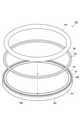
静電チャック20の外周領域上には、フォーカスリングFRが配置される。フォーカスリングFRは、略環状板形状を有しており、例えばシリコンから形成される。フォーカスリングFRは、基板Wのエッジを囲むように配置される。 A focus ring FR is arranged on the outer peripheral region of the
プラズマ処理装置10は、上部電極30を更に備える。上部電極30は、ステージ16の上方に設けられる。上部電極30は、部材32と共にチャンバ本体12の上部開口を閉じる。部材32は、絶縁性を有する。上部電極30は、この部材32を介してチャンバ本体12の上部に支持される。後述するように、高周波電源61が下部電極18に電気的に接続されている場合には、上部電極30は接地電位に接続される。 The
上部電極30は、天板34及び支持体36を含む。天板34の下面は、チャンバ12cを画成する。天板34には、複数のガス吐出孔34aが設けられる。複数のガス吐出孔34aの各々は、天板34を板厚方向(鉛直方向)に貫通する。この天板34は、例えばシリコンから形成される。あるいは、天板34は、アルミニウム製の母材の表面に耐プラズマ性の膜を設けた構造を有し得る。この膜は、陽極酸化処理によって形成された膜、又は、酸化イットリウムから形成された膜といったセラミック製の膜であり得る。 The
支持体36は、天板34を着脱自在に支持する部品である。支持体36は、例えばアルミニウムといった導電性材料から形成され得る。支持体36の内部には、ガス拡散室36aが設けられている。ガス拡散室36aからは、複数のガス孔36bが下方に延びる。複数のガス孔36bは、複数のガス吐出孔34aにそれぞれ連通する。支持体36には、ガス拡散室36aにガスを導くガス導入口36cが形成されており、このガス導入口36cには、ガス供給管38が接続される。 The
ガス供給管38には、バルブ群42及び流量制御器群44を介して、ガスソース群40が接続される。ガスソース群40は、複数のガスソースを含む。バルブ群42は複数のバルブを含んでおり、流量制御器群44は複数の流量制御器を含む。流量制御器群44の複数の流量制御器の各々は、マスフローコントローラ又は圧力制御式の流量制御器である。ガスソース群40の複数のガスソースはそれぞれ、バルブ群42の対応のバルブ及び流量制御器群44の対応の流量制御器を介して、ガス供給管38に接続される。プラズマ処理装置10は、ガスソース群40の複数のガスソースのうち選択された一以上のガスソースからのガスを、個別に調整された流量で、チャンバ12cに供給することが可能である。 The
筒状部28とチャンバ本体12の側壁との間には、バッフルプレート48が設けられる。バッフルプレート48は、例えば、アルミニウム製の母材に酸化イットリウム等のセラミックを被覆することにより構成され得る。このバッフルプレート48には、多数の貫通孔が形成される。バッフルプレート48の下方においては、排気管52がチャンバ本体12の底部に接続される。この排気管52には、排気装置50が接続される。排気装置50は、自動圧力制御弁といった圧力制御器、及び、ターボ分子ポンプなどの真空ポンプを有しており、チャンバ12cを減圧することができる。 A
プラズマ処理装置10は、高周波電源61を更に備えている。高周波電源61は、プラズマ生成用の高周波を発生する電源である。高周波は、27~100MHzの範囲内の周波数、例えば60MHzの周波数を有する。高周波電源61は、整合器65及び電極プレート21を介して、下部電極18に接続される。整合器65は、高周波電源61の出力インピーダンスと負荷側(下部電極18側)のインピーダンスを整合させる。なお、高周波電源61は、整合器65を介して上部電極30に接続されていてもよい。The
プラズマ処理装置10は、可変直流電源70を更に備える。可変直流電源70は、フォーカスリングFRに印加される負極性の直流電圧を発生する電源である。可変直流電源70は、一例として、フォーカスリング及び基板のエッジ領域の上方におけるシースの形状を制御するために、フォーカスリングFRに負極性の直流電圧を印加する。 The
プラズマ処理装置10は、主制御部MCを更に備え得る。主制御部MCは、プロセッサ、記憶装置、入力装置、表示装置等を備えるコンピュータであり、プラズマ処理装置10の各部を制御する。具体的に、主制御部MCは、記憶装置に記憶されている制御プログラムを実行し、当該記憶装置に記憶されているレシピデータに基づいてプラズマ処理装置10の各部を制御する。これにより、プラズマ処理装置10は、レシピデータによって指定されたプロセスを実行するようになっている。 The
[支持アセンブリ]
図2は、図1に示される支持アセンブリの一部拡大断面図である。図3は、図1に示される支持アセンブリの分解図である。図2,3に示されるように、支持アセンブリ1は、静電チャック20と、下部電極18と、少なくとも1つの導電部材82と、絶縁部材80とを備える。[Support assembly]
FIG. 2 is a partially enlarged cross-sectional view of the support assembly shown in FIG. FIG. 3 is an exploded view of the support assembly shown in FIG. As shown in FIGS. 2 and 3, the
下部電極18は、その上面に、静電チャック20を支持するチャック支持面18aと、フォーカスリングを支持するリング支持面18bとを有する。チャック支持面18aは、下部電極18の上面における中央の円形領域であり、静電チャック20と同一面積を有する。リング支持面18bは、下部電極18の上面におけるエッジ領域であり、チャック支持面18aを囲むように形成される。リング支持面18b及び下部電極18の側面18cの表面は、絶縁性を有するように表面改質処理が施される。一例として、リング支持面18b及び側面18cの表面には、アルミナ溶射膜などの絶縁膜18dが形成される。 The
絶縁膜18dが形成されたリング支持面18b上には、コンタクト電極81が形成される。コンタクト電極81は、リング支持面18bの全周にわたって形成される。コンタクト電極81は、金属などの導電性を有する材料から形成される。一例として、コンタクト電極81は、タングステンを溶射して形成される。なお、コンタクト電極81は、電気的な接続端子として機能すればよい。つまり、コンタクト電極81は、連続したリング形状に限定されず、リング支持面18bの全周の一部に形成されてもよい。 A
コンタクト電極81は、可変直流電源70に接続されている。可変直流電源70は、供給する電圧を変更可能に構成される。下部電極18のリング支持面18bには、コンタクト電極81に対応した位置に、下部電極18の底部まで延びる貫通孔18eが形成される。貫通孔18eの内部は、絶縁性を有する充填部材83で充填され、コンタクト電極81と可変直流電源70とを接続する配線が収容される。なお、コンタクト電極81は、可変直流電源70に替えて、スイッチ回路及び直流電源に接続されていてもよい。 The
絶縁部材80は、下部電極18のリング支持面18bとフォーカスリングFRとの間に介在する。絶縁部材80は、リング状のシート部材であり、その上面80aがフォーカスリングFRに接触し、その下面80bが下部電極18に接触する。絶縁部材80は、弾性及び接着性を有してもよい。絶縁部材80は、例えばシリコーン(Silicone)などを主成分とする合成樹脂から形成される。 The insulating
絶縁部材80は、少なくとも1つの導電部材82を囲む状態で配置される。より具体的な一例として、絶縁部材80は、少なくとも1つの導電部材82の側方を囲んでいる。導電部材82は、絶縁部材80の厚さ方向に延在する線状部材である。導電部材82は、絶縁部材80の内部に埋め込まれる。導電部材82は、絶縁部材80の面内方向の中央に埋め込まれてもよい。導電部材82は、その両端が絶縁部材80の上面80aと下面80bとから突出した状態であってもよいし、リング支持面18bとフォーカスリングFRとの間に介在したときに、その両端が絶縁部材80の上面80aと下面80bとから突出するように絶縁部材80に埋め込まれていてもよい。導電部材82は、直線形状であってもよいし、湾曲していてもよい。導電部材82は、コンタクト電極81と鉛直方向からみて重なる位置に配置される。図中では、複数の導電部材82が、リング状の絶縁部材80の全周にわたって配置される。導電部材82の上端がフォーカスリングFRの下面と接触し、導電部材82の下端がコンタクト電極81と接触する。これにより、導電部材82は、コンタクト電極81とフォーカスリングFRとを電気的に接続する。 The insulating
フォーカスリングFRは、下部電極18と絶縁されるとともに、導電部材82及びコンタクト電極81を介して、可変直流電源70から電圧が供給される。 The focus ring FR is insulated from the
[支持アセンブリの組立方法]
図4は、支持アセンブリの組立方法の一例である。図4に示されるように、最初に、準備工程(ステップS10)として、静電チャック20と、フォーカスリングFRと、チャック支持面18a及びリング支持面18bを有する下部電極18と、導電部材82を囲む絶縁部材80と、が準備される。[Assembly method of support assembly]
FIG. 4 is an example of a method of assembling a support assembly. As shown in FIG. 4, first, as a preparatory step (step S10), an
続いて、電極形成工程(ステップS12)として、下部電極18にコンタクト電極81が溶射される。 Subsequently, as an electrode forming step (step S12), the
続いて、装着工程(ステップS14)として、静電チャック20がチャック支持面18aに接着剤で固定されるとともに、リング支持面18b上に絶縁部材80がコンタクト電極81と導電部材82とが対向するように配置され、絶縁部材80上にフォーカスリングFRが配置され、コンタクト電極81、導電部材82、及び、フォーカスリングFRが電気的に接続された状態で固定される。絶縁部材80が粘着性を有する場合、下部電極18、絶縁部材80及びフォーカスリングFRの順に積層し、厚さ方向に押圧することで、固定配置される。 Subsequently, as a mounting step (step S14), the
[第1実施形態のまとめ]
支持アセンブリ1では、下部電極18のリング支持面18bとフォーカスリングFRとの間に、少なくとも1つの導電部材82を囲む状態で絶縁部材80が介在する。これにより、異常放電を抑制することができる。また、フォーカスリングFRは、導電部材82によってコンタクト電極81に接続される。このため、コンタクト電極81に印加された直流電圧は、導電部材82を介してフォーカスリングFRに印加される。このように、支持アセンブリ1は、装置に大きな変更を加えることなく、異常放電を抑制しながらフォーカスリングFRに直流電圧を印加することができる。よって、支持アセンブリ1は、簡易な構成で、異常放電を抑制しつつ、フォーカスリングFRへの直流電圧印加を実現することができる。[Summary of the first embodiment]
In the
支持アセンブリ1では、フォーカスリングFRの全周に直流電圧が印加されるので、電気的及び熱的な偏りを低減することができる。 In the
[第2実施形態]
第2実施形態に係る支持アセンブリ1Aは、支持アセンブリ1と比較して、コンタクト電極81に接続される電源が相違し、その他は同一である。第2実施形態では、第1実施形態と重複する説明は繰り返さない。[Second Embodiment]
The
図5は、第2実施形態に係る支持アセンブリの一例である。図5に示されるように、支持アセンブリ1Aのコンタクト電極81は、整合器95を介して交流電源90に接続される。その他の構成は、第1実施形態と同一である。 FIG. 5 is an example of the support assembly according to the second embodiment. As shown in FIG. 5, the
[第2実施形態のまとめ]
支持アセンブリ1Aでは、下部電極18のリング支持面18bとフォーカスリングFRとの間に、少なくとも1つの導電部材82を囲む状態で絶縁部材80が介在する。これにより、異常放電を抑制することができる。また、フォーカスリングFRは、導電部材82によってコンタクト電極81に接続される。このため、コンタクト電極81に印加された交流電圧は、導電部材82を介してフォーカスリングFRに印加される。このように、支持アセンブリ1Aは、装置に大きな変更を加えることなく、異常放電を抑制しながらフォーカスリングFRに交流電圧を直接印加することができる。よって、支持アセンブリ1Aは、簡易な構成で、異常放電を抑制しつつ、フォーカスリングFRへの交流電圧印加を実現することができる。[Summary of the second embodiment]
In the
支持アセンブリ1Aでは、フォーカスリングFRの全周に交流電圧が印加されるので、電気的及び熱的な偏りを低減することができる。 In the
[第3実施形態]
第3実施形態に係る支持アセンブリ1Bは、支持アセンブリ1と比較して、下部電極18に貫通孔18eが形成されておらず、下部電極18に可変直流電源70が直接接続される点が相違し、その他は同一である。第3実施形態では、第1実施形態と重複する説明は繰り返さない。[Third Embodiment]
The
図6は、第3実施形態に係る支持アセンブリの一例である。図7は、図6に示される支持アセンブリの分解図である。図6及び図7に示されるように、支持アセンブリ1Bに電圧を供給する可変直流電源70は、下部電極18に接続される。下部電極18に印加された直流電圧は、下部電極18に印加された高周波と重畳し、フォーカスリングFRに供給される。その他の構成は、第1実施形態と同一である。 FIG. 6 is an example of the support assembly according to the third embodiment. FIG. 7 is an exploded view of the support assembly shown in FIG. As shown in FIGS. 6 and 7, the variable
[第3実施形態のまとめ]
支持アセンブリ1Bでは、下部電極18のリング支持面18bとフォーカスリングFRとの間に、少なくとも1つの導電部材82を囲む状態で絶縁部材80が介在する。これにより、異常放電を抑制することができる。また、フォーカスリングFRは、導電部材82によってコンタクト電極81に接続される。このため、コンタクト電極81に印加された直流電圧は、導電部材82を介してフォーカスリングFRに印加される。このように、支持アセンブリ1Bは、装置に大きな変更を加えることなく、異常放電を抑制しながらフォーカスリングFRに直流電圧を印加することができる。よって、支持アセンブリ1Bは、簡易な構成で、異常放電を抑制しつつ、フォーカスリングFRへの直流電圧印加を実現することができる。[Summary of the third embodiment]
In the
支持アセンブリ1Bでは、フォーカスリングFRの全周に直流電圧が印加されるので、電気的及び熱的な偏りを低減することができる。 In the
[変形例]
以上、種々の実施形態について説明してきたが、上述した実施形態に限定されることなく種々の変形態様を構成可能である。例えば、上述した種々の実施形態に係るプラズマ処理装置は容量結合型のプラズマ処理装置である。変形態様におけるプラズマ処理装置は、誘導結合型のプラズマ処理装置であってもよい。また、フォーカスリングFRは、分割されていてもよい。この場合、分割されたフォーカスリングFRごとに電圧を印加することができる。[Modification example]
Although various embodiments have been described above, various modifications can be configured without being limited to the above-described embodiments. For example, the plasma processing apparatus according to the various embodiments described above is a capacitively coupled plasma processing apparatus. The plasma processing device in the modified mode may be an inductively coupled plasma processing device. Further, the focus ring FR may be divided. In this case, a voltage can be applied to each of the divided focus ring FRs.
以下、発明者が確認した実施形態の効果について説明する。
(フォーカスリングの全周に電圧印加した場合の効果確認)
フォーカスリングの全周に電圧印加可能な実施例1と、フォーカスリングの一部に電圧印加可能な実施例2とを用意した。
(実施例1)
第1実施形態の支持アセンブリ1を作成した。下部電極18のリング支持面18bにコンタクト電極81をリング支持面18bの全周にわたって形成した。その後、全周に導電部材82が埋め込まれた絶縁部材80を用いて、リング支持面18bにフォーカスリングFRを固定配置した。
(実施例2)
実施例2は、実施例1と比較すると、下部電極18のリング支持面18bにコンタクト電極81をリング支持面18bの一部分に形成した点、コンタクト電極81に対応する位置に絶縁部材80を配置した点を除き、同一である。周方向に間隔を空けて四カ所にコンタクト電極81及び絶縁部材80を配置した。Hereinafter, the effects of the embodiments confirmed by the inventor will be described.
(Check the effect when voltage is applied to the entire circumference of the focus ring)
Example 1 in which a voltage can be applied to the entire circumference of the focus ring and Example 2 in which a voltage can be applied to a part of the focus ring are prepared.
(Example 1)
The
(Example 2)
In Example 2, as compared with Example 1, the insulating
(発熱評価)
実施例1及び実施例2のそれぞれのフォーカスリングFRに直流電圧を印加しつつ、下部電極18に高周波を印加し、フォーカスリングFRの温度経過を計測した。高周波は、3.2MHz/1kWとした。結果を図8に示す。図8は、フォーカスリングの発熱量を評価したグラフである。横軸は、高周波印加後の経過時間であり、縦軸は、フォーカスリングFRの温度である。フォーカスリングFRの温度は、計測箇所の最高温度をプロットしている。実施例1は実線の波形であり、実施例2は破線の波形である。(Fever evaluation)
While applying a DC voltage to each of the focus ring FRs of Examples 1 and 2, a high frequency was applied to the
図8に示されるように、破線のグラフで示される実施例2は、高周波印加後にフォーカスリングFRの温度が急激に上昇し、開始から約100秒程度でΔT1(約36.9℃)まで上昇した。なお、フォーカスリングFRの破損を考慮して、ΔT1上昇した時点で計測を終了した。一方、実線のグラフで示される実施例1は、フォーカスリングFRの温度は時間経過とともに緩やかに上昇し、開始から約250秒経過してもΔT2(約5.4℃)しか上昇しなかった。このように、フォーカスリングFRの全周に電圧印加した場合、フォーカスリングFRの一部に電圧印加した場合と比べて、発熱量が抑えられることが確認された。 As shown in FIG. 8, in Example 2 shown by the broken line graph, the temperature of the focus ring FR rises sharply after the application of high frequency, and rises to ΔT1 (about 36.9 ° C.) in about 100 seconds from the start. did. In consideration of damage to the focus ring FR, the measurement was terminated when ΔT1 increased. On the other hand, in Example 1 shown by the solid line graph, the temperature of the focus ring FR gradually increased with the passage of time, and only ΔT2 (about 5.4 ° C.) increased even after about 250 seconds had passed from the start. As described above, it was confirmed that when the voltage was applied to the entire circumference of the focus ring FR, the calorific value was suppressed as compared with the case where the voltage was applied to a part of the focus ring FR.
実施例1及び実施例2のそれぞれのフォーカスリングFRに直流電圧を印加しつつ、下部電極18に高周波を印加し、フォーカスリングFRの温度分布を計測した。図9は、フォーカスリングの温度分布を評価した結果である。図9の(A)は、実施例1の温度分布であり、図9の(B)は、実施例2の温度分布である。図9に示されるように、実施例1の温度分布の方が、実施例2の温度分布よりも、温度勾配が少ないことが確認された。このため、フォーカスリングの全周に電圧が印加されることで、熱的な偏りを低減することができることが確認された。 While applying a DC voltage to each of the focus ring FRs of Examples 1 and 2, a high frequency was applied to the
10…プラズマ処理装置、16…ステージ、18…下部電極、18a…チャック支持面、18b…リング支持面、20…静電チャック、61…高周波電源、70…可変直流電源、80…絶縁部材、81…コンタクト電極、82…導電部材、FR…フォーカスリング。 10 ... Plasma processing device, 16 ... Stage, 18 ... Lower electrode, 18a ... Chuck support surface, 18b ... Ring support surface, 20 ... Electrostatic chuck, 61 ... High frequency power supply, 70 ... Variable DC power supply, 80 ... Insulation member, 81 ... contact electrode, 82 ... conductive member, FR ... focus ring.
Claims (4)
Translated fromJapanese前記静電チャックを支持するチャック支持面と、前記チャック支持面を囲むように形成され、フォーカスリングを支持するリング支持面とを有し、前記リング支持面上にコンタクト電極が形成された、下部電極と、
前記コンタクト電極と前記フォーカスリングとを電気的に接続する少なくとも1つの導電部材と、
前記少なくとも1つの導電部材を囲む状態で前記下部電極のリング支持面と前記フォーカスリングとの間に介在する絶縁部材と、
を有する支持アセンブリと、
前記支持アセンブリを収容するチャンバと、
前記下部電極に電圧を印加する第1電源と、
前記コンタクト電極に電圧を印加する第2電源と、
を備える、プラズマ処理装置。With an electrostatic chuck,
A lower portion having a chuck support surface that supports the electrostatic chuck and a ring support surface that is formed so as to surround the chuck support surface and supports the focus ring, and a contact electrode is formed on the ring support surface. With electrodes
At least one conductive member that electrically connects the contact electrode and the focus ring,
An insulating member interposed between the ring support surface of the lower electrode and the focus ring while surrounding the at least one conductive member.
With support assembly and
A chamber containing the support assembly and
A first power source that applies a voltage to the lower electrode,
A second power source that applies a voltage to the contact electrode,
A plasma processing device.
前記少なくとも1つの導電部材は、リング状の前記絶縁部材の全周にわたって配置される、請求項1に記載のプラズマ処理装置。The contact electrode is formed over the entire circumference of the ring support surface and is formed.
Theplasma processing apparatus according to claim 1, wherein the at least one conductive member is arranged over the entire circumference of the ring-shaped insulating member.
前記少なくとも1つの導電部材は、前記絶縁部材の厚さ方向に延在する線状部材である、請求項1又は2に記載のプラズマ処理装置。The upper surface of the insulating member is in contact with the focus ring, and the lower surface thereof is in contact with the lower electrode.
Theplasma processing apparatus according to claim 1 or 2, wherein the at least one conductive member is a linear member extending in the thickness direction of the insulating member.
前記貫通孔の内部には、前記コンタクト電極と電源とを接続する配線が収容される、請求項1~3の何れか一項に記載のプラズマ処理装置。The plasma processing apparatus according to any one of claims 1 to 3, wherein wiring for connecting the contact electrode and the power supply is housed inside the through hole.
Priority Applications (5)
| Application Number | Priority Date | Filing Date | Title |
|---|---|---|---|
| JP2017231776AJP7033441B2 (en) | 2017-12-01 | 2017-12-01 | Plasma processing equipment |
| TW107141998ATWI803539B (en) | 2017-12-01 | 2018-11-26 | Support assembly and support assembly assembling method |
| CN201811434243.0ACN109872939B (en) | 2017-12-01 | 2018-11-28 | Support assembly and method of assembling a support assembly |
| KR1020180150530AKR102603893B1 (en) | 2017-12-01 | 2018-11-29 | Plasma processing apparatus |
| US16/206,100US11201038B2 (en) | 2017-12-01 | 2018-11-30 | Support assembly and support assembly assembling method |
Applications Claiming Priority (1)
| Application Number | Priority Date | Filing Date | Title |
|---|---|---|---|
| JP2017231776AJP7033441B2 (en) | 2017-12-01 | 2017-12-01 | Plasma processing equipment |
Publications (3)
| Publication Number | Publication Date |
|---|---|
| JP2019102638A JP2019102638A (en) | 2019-06-24 |
| JP2019102638A5 JP2019102638A5 (en) | 2020-10-08 |
| JP7033441B2true JP7033441B2 (en) | 2022-03-10 |
Family
ID=66659508
Family Applications (1)
| Application Number | Title | Priority Date | Filing Date |
|---|---|---|---|
| JP2017231776AActiveJP7033441B2 (en) | 2017-12-01 | 2017-12-01 | Plasma processing equipment |
Country Status (5)
| Country | Link |
|---|---|
| US (1) | US11201038B2 (en) |
| JP (1) | JP7033441B2 (en) |
| KR (1) | KR102603893B1 (en) |
| CN (1) | CN109872939B (en) |
| TW (1) | TWI803539B (en) |
Families Citing this family (41)
| Publication number | Priority date | Publication date | Assignee | Title |
|---|---|---|---|---|
| CN108369922B (en) | 2016-01-26 | 2023-03-21 | 应用材料公司 | Wafer edge ring lifting solution |
| CN116110846A (en) | 2016-01-26 | 2023-05-12 | 应用材料公司 | Wafer edge ring lift solution |
| US10553404B2 (en) | 2017-02-01 | 2020-02-04 | Applied Materials, Inc. | Adjustable extended electrode for edge uniformity control |
| US10510575B2 (en) | 2017-09-20 | 2019-12-17 | Applied Materials, Inc. | Substrate support with multiple embedded electrodes |
| US11075105B2 (en) | 2017-09-21 | 2021-07-27 | Applied Materials, Inc. | In-situ apparatus for semiconductor process module |
| US10555412B2 (en) | 2018-05-10 | 2020-02-04 | Applied Materials, Inc. | Method of controlling ion energy distribution using a pulse generator with a current-return output stage |
| US10600623B2 (en) | 2018-05-28 | 2020-03-24 | Applied Materials, Inc. | Process kit with adjustable tuning ring for edge uniformity control |
| US11935773B2 (en) | 2018-06-14 | 2024-03-19 | Applied Materials, Inc. | Calibration jig and calibration method |
| US10847347B2 (en) | 2018-08-23 | 2020-11-24 | Applied Materials, Inc. | Edge ring assembly for a substrate support in a plasma processing chamber |
| US11476145B2 (en) | 2018-11-20 | 2022-10-18 | Applied Materials, Inc. | Automatic ESC bias compensation when using pulsed DC bias |
| US11289310B2 (en) | 2018-11-21 | 2022-03-29 | Applied Materials, Inc. | Circuits for edge ring control in shaped DC pulsed plasma process device |
| KR102827481B1 (en) | 2019-01-22 | 2025-06-30 | 어플라이드 머티어리얼스, 인코포레이티드 | Feedback loop to control pulse voltage waveform |
| US11508554B2 (en) | 2019-01-24 | 2022-11-22 | Applied Materials, Inc. | High voltage filter assembly |
| US10784089B2 (en) | 2019-02-01 | 2020-09-22 | Applied Materials, Inc. | Temperature and bias control of edge ring |
| US12009236B2 (en) | 2019-04-22 | 2024-06-11 | Applied Materials, Inc. | Sensors and system for in-situ edge ring erosion monitor |
| KR102726757B1 (en)* | 2019-12-24 | 2024-11-08 | 주식회사 제우스 | Substrate processing apparatus |
| JP7330115B2 (en)* | 2020-02-07 | 2023-08-21 | 東京エレクトロン株式会社 | Plasma processing apparatus and plasma processing method |
| US11668553B2 (en) | 2020-02-14 | 2023-06-06 | Applied Materials Inc. | Apparatus and method for controlling edge ring variation |
| JP7454961B2 (en)* | 2020-03-05 | 2024-03-25 | 東京エレクトロン株式会社 | plasma processing equipment |
| US11848176B2 (en) | 2020-07-31 | 2023-12-19 | Applied Materials, Inc. | Plasma processing using pulsed-voltage and radio-frequency power |
| KR102751528B1 (en) | 2020-09-01 | 2025-01-07 | 삼성전자주식회사 | Plasma processing equipment |
| JP7489896B2 (en)* | 2020-10-22 | 2024-05-24 | 東京エレクトロン株式会社 | Plasma Processing Equipment |
| US11798790B2 (en) | 2020-11-16 | 2023-10-24 | Applied Materials, Inc. | Apparatus and methods for controlling ion energy distribution |
| US11901157B2 (en) | 2020-11-16 | 2024-02-13 | Applied Materials, Inc. | Apparatus and methods for controlling ion energy distribution |
| WO2022201351A1 (en)* | 2021-03-24 | 2022-09-29 | 株式会社日立ハイテク | Plasma treatment device and plasma treatment method |
| US11495470B1 (en) | 2021-04-16 | 2022-11-08 | Applied Materials, Inc. | Method of enhancing etching selectivity using a pulsed plasma |
| US11791138B2 (en) | 2021-05-12 | 2023-10-17 | Applied Materials, Inc. | Automatic electrostatic chuck bias compensation during plasma processing |
| US11948780B2 (en) | 2021-05-12 | 2024-04-02 | Applied Materials, Inc. | Automatic electrostatic chuck bias compensation during plasma processing |
| US11967483B2 (en) | 2021-06-02 | 2024-04-23 | Applied Materials, Inc. | Plasma excitation with ion energy control |
| US20220399185A1 (en) | 2021-06-09 | 2022-12-15 | Applied Materials, Inc. | Plasma chamber and chamber component cleaning methods |
| US12394596B2 (en) | 2021-06-09 | 2025-08-19 | Applied Materials, Inc. | Plasma uniformity control in pulsed DC plasma chamber |
| US11810760B2 (en) | 2021-06-16 | 2023-11-07 | Applied Materials, Inc. | Apparatus and method of ion current compensation |
| US11569066B2 (en) | 2021-06-23 | 2023-01-31 | Applied Materials, Inc. | Pulsed voltage source for plasma processing applications |
| US11776788B2 (en) | 2021-06-28 | 2023-10-03 | Applied Materials, Inc. | Pulsed voltage boost for substrate processing |
| US11476090B1 (en) | 2021-08-24 | 2022-10-18 | Applied Materials, Inc. | Voltage pulse time-domain multiplexing |
| US12106938B2 (en) | 2021-09-14 | 2024-10-01 | Applied Materials, Inc. | Distortion current mitigation in a radio frequency plasma processing chamber |
| KR20230067256A (en)* | 2021-11-09 | 2023-05-16 | 삼성전자주식회사 | chuck assembly, manufacturing apparatus of semiconductor device including the same and manufacturing method of semiconductor device |
| US11972924B2 (en) | 2022-06-08 | 2024-04-30 | Applied Materials, Inc. | Pulsed voltage source for plasma processing applications |
| US12315732B2 (en) | 2022-06-10 | 2025-05-27 | Applied Materials, Inc. | Method and apparatus for etching a semiconductor substrate in a plasma etch chamber |
| US12272524B2 (en) | 2022-09-19 | 2025-04-08 | Applied Materials, Inc. | Wideband variable impedance load for high volume manufacturing qualification and on-site diagnostics |
| US12111341B2 (en) | 2022-10-05 | 2024-10-08 | Applied Materials, Inc. | In-situ electric field detection method and apparatus |
Citations (7)
| Publication number | Priority date | Publication date | Assignee | Title |
|---|---|---|---|---|
| JP2004109121A (en) | 2002-08-27 | 2004-04-08 | Jsr Corp | Anisotropic conductive sheet and probe for impedance measurement |
| JP2009239222A (en) | 2008-03-28 | 2009-10-15 | Tokyo Electron Ltd | Plasma etching apparatus, plasma etching method and computer-readable storage medium |
| JP2011210958A (en) | 2010-03-30 | 2011-10-20 | Tokyo Electron Ltd | Plasma processing apparatus and method of manufacturing semiconductor device |
| JP2012209359A (en) | 2011-03-29 | 2012-10-25 | Tokyo Electron Ltd | Plasma processing equipment |
| JP2013168690A (en) | 2013-06-06 | 2013-08-29 | Tokyo Electron Ltd | Plasma processing apparatus, focus ring, and focus ring component |
| JP2014022518A (en) | 2012-07-17 | 2014-02-03 | Tokyo Electron Ltd | Lower electrode and plasma processing device |
| JP2017055100A (en) | 2015-07-13 | 2017-03-16 | ラム リサーチ コーポレーションLam Research Corporation | Sheath and wafer profile adjustment at the extreme edge through ion trajectory control and plasma motion confined to the edge |
Family Cites Families (16)
| Publication number | Priority date | Publication date | Assignee | Title |
|---|---|---|---|---|
| JP4559595B2 (en)* | 2000-07-17 | 2010-10-06 | 東京エレクトロン株式会社 | Apparatus for placing object to be processed and plasma processing apparatus |
| US7662723B2 (en)* | 2005-12-13 | 2010-02-16 | Lam Research Corporation | Methods and apparatus for in-situ substrate processing |
| JP5657262B2 (en)* | 2009-03-27 | 2015-01-21 | 東京エレクトロン株式会社 | Plasma processing equipment |
| JP5227264B2 (en)* | 2009-06-02 | 2013-07-03 | 東京エレクトロン株式会社 | Plasma processing apparatus, plasma processing method, program |
| JP5357639B2 (en)* | 2009-06-24 | 2013-12-04 | 株式会社日立ハイテクノロジーズ | Plasma processing apparatus and plasma processing method |
| JP5584517B2 (en)* | 2010-05-12 | 2014-09-03 | 東京エレクトロン株式会社 | Plasma processing apparatus and semiconductor device manufacturing method |
| WO2012056807A1 (en)* | 2010-10-25 | 2012-05-03 | 日本碍子株式会社 | Ceramic material, laminated body, member for semiconductor manufacturing device, and sputtering target member |
| WO2013078420A2 (en)* | 2011-11-24 | 2013-05-30 | Lam Research Corporation | Symmetric rf return path liner |
| JP5970268B2 (en)* | 2012-07-06 | 2016-08-17 | 株式会社日立ハイテクノロジーズ | Plasma processing apparatus and processing method |
| JP6219229B2 (en)* | 2014-05-19 | 2017-10-25 | 東京エレクトロン株式会社 | Heater feeding mechanism |
| CN108140606B (en)* | 2015-10-21 | 2022-05-24 | 住友大阪水泥股份有限公司 | Electrostatic chuck device |
| US10062599B2 (en)* | 2015-10-22 | 2018-08-28 | Lam Research Corporation | Automated replacement of consumable parts using interfacing chambers |
| US9852889B1 (en)* | 2016-06-22 | 2017-12-26 | Lam Research Corporation | Systems and methods for controlling directionality of ions in an edge region by using an electrode within a coupling ring |
| JP2018006299A (en)* | 2016-07-08 | 2018-01-11 | 東芝メモリ株式会社 | Processing object susceptor for plasma processing apparatus, plasma processing apparatus and plasma processing method |
| US20180061696A1 (en)* | 2016-08-23 | 2018-03-01 | Applied Materials, Inc. | Edge ring or process kit for semiconductor process module |
| US20190119815A1 (en)* | 2017-10-24 | 2019-04-25 | Applied Materials, Inc. | Systems and processes for plasma filtering |
- 2017
- 2017-12-01JPJP2017231776Apatent/JP7033441B2/enactiveActive
- 2018
- 2018-11-26TWTW107141998Apatent/TWI803539B/enactive
- 2018-11-28CNCN201811434243.0Apatent/CN109872939B/enactiveActive
- 2018-11-29KRKR1020180150530Apatent/KR102603893B1/enactiveActive
- 2018-11-30USUS16/206,100patent/US11201038B2/enactiveActive
Patent Citations (7)
| Publication number | Priority date | Publication date | Assignee | Title |
|---|---|---|---|---|
| JP2004109121A (en) | 2002-08-27 | 2004-04-08 | Jsr Corp | Anisotropic conductive sheet and probe for impedance measurement |
| JP2009239222A (en) | 2008-03-28 | 2009-10-15 | Tokyo Electron Ltd | Plasma etching apparatus, plasma etching method and computer-readable storage medium |
| JP2011210958A (en) | 2010-03-30 | 2011-10-20 | Tokyo Electron Ltd | Plasma processing apparatus and method of manufacturing semiconductor device |
| JP2012209359A (en) | 2011-03-29 | 2012-10-25 | Tokyo Electron Ltd | Plasma processing equipment |
| JP2014022518A (en) | 2012-07-17 | 2014-02-03 | Tokyo Electron Ltd | Lower electrode and plasma processing device |
| JP2013168690A (en) | 2013-06-06 | 2013-08-29 | Tokyo Electron Ltd | Plasma processing apparatus, focus ring, and focus ring component |
| JP2017055100A (en) | 2015-07-13 | 2017-03-16 | ラム リサーチ コーポレーションLam Research Corporation | Sheath and wafer profile adjustment at the extreme edge through ion trajectory control and plasma motion confined to the edge |
Also Published As
| Publication number | Publication date |
|---|---|
| US11201038B2 (en) | 2021-12-14 |
| TW201929084A (en) | 2019-07-16 |
| CN109872939A (en) | 2019-06-11 |
| KR102603893B1 (en) | 2023-11-17 |
| US20190172688A1 (en) | 2019-06-06 |
| JP2019102638A (en) | 2019-06-24 |
| KR20190065141A (en) | 2019-06-11 |
| TWI803539B (en) | 2023-06-01 |
| CN109872939B (en) | 2022-01-28 |
Similar Documents
| Publication | Publication Date | Title |
|---|---|---|
| JP7033441B2 (en) | Plasma processing equipment | |
| US11476095B2 (en) | Electrostatic chuck and plasma processing apparatus | |
| KR102428060B1 (en) | Mounting table and plasma processing apparatus | |
| KR102383357B1 (en) | Mounting table and substrate processing apparatus | |
| JP6442296B2 (en) | Mounting table and plasma processing apparatus | |
| US10741368B2 (en) | Plasma processing apparatus | |
| TWI721062B (en) | Plasma processing method and plasma processing device | |
| TWI762551B (en) | Plasma processing apparatus | |
| JP6960390B2 (en) | Power supply structure and plasma processing equipment | |
| KR102414854B1 (en) | Plasma processing apparatus | |
| JP6424049B2 (en) | Plasma processing equipment | |
| JP7145041B2 (en) | Substrate support, plasma processing apparatus, and focus ring | |
| KR101898079B1 (en) | Plasma processing apparatus | |
| JP7145042B2 (en) | Substrate support and plasma processing equipment | |
| JP2020061454A (en) | Substrate support assembly, plasma processing apparatus, and plasma processing method | |
| WO2022259793A1 (en) | Plasma treatment device | |
| JP6932070B2 (en) | Focus ring and semiconductor manufacturing equipment | |
| JP7500397B2 (en) | Plasma processing apparatus, its manufacturing method, and plasma processing method | |
| JP2024002949A (en) | Plasma processing device, ring, electrostatic chuck inspection method, and substrate processing method |
Legal Events
| Date | Code | Title | Description |
|---|---|---|---|
| A521 | Request for written amendment filed | Free format text:JAPANESE INTERMEDIATE CODE: A523 Effective date:20200826 | |
| A621 | Written request for application examination | Free format text:JAPANESE INTERMEDIATE CODE: A621 Effective date:20200826 | |
| A977 | Report on retrieval | Free format text:JAPANESE INTERMEDIATE CODE: A971007 Effective date:20210806 | |
| A131 | Notification of reasons for refusal | Free format text:JAPANESE INTERMEDIATE CODE: A131 Effective date:20210817 | |
| A521 | Request for written amendment filed | Free format text:JAPANESE INTERMEDIATE CODE: A523 Effective date:20211018 | |
| TRDD | Decision of grant or rejection written | ||
| A01 | Written decision to grant a patent or to grant a registration (utility model) | Free format text:JAPANESE INTERMEDIATE CODE: A01 Effective date:20220201 | |
| A61 | First payment of annual fees (during grant procedure) | Free format text:JAPANESE INTERMEDIATE CODE: A61 Effective date:20220228 | |
| R150 | Certificate of patent or registration of utility model | Ref document number:7033441 Country of ref document:JP Free format text:JAPANESE INTERMEDIATE CODE: R150 | |
| R250 | Receipt of annual fees | Free format text:JAPANESE INTERMEDIATE CODE: R250 |