JP7027176B2 - Semiconductor device - Google Patents
Semiconductor deviceDownload PDFInfo
- Publication number
- JP7027176B2 JP7027176B2JP2018007919AJP2018007919AJP7027176B2JP 7027176 B2JP7027176 B2JP 7027176B2JP 2018007919 AJP2018007919 AJP 2018007919AJP 2018007919 AJP2018007919 AJP 2018007919AJP 7027176 B2JP7027176 B2JP 7027176B2
- Authority
- JP
- Japan
- Prior art keywords
- resistance element
- semiconductor device
- capacitor
- circuit
- power supply
- Prior art date
- Legal status (The legal status is an assumption and is not a legal conclusion. Google has not performed a legal analysis and makes no representation as to the accuracy of the status listed.)
- Active
Links
- 239000004065semiconductorSubstances0.000titleclaimsdescription33
- 239000003990capacitorSubstances0.000claimsdescription28
- 239000000758substrateSubstances0.000claimsdescription9
- 239000010410layerSubstances0.000claimsdescription5
- 239000011229interlayerSubstances0.000claimsdescription4
- 239000012212insulatorSubstances0.000claimsdescription3
- 230000001681protective effectEffects0.000description8
- YMWUJEATGCHHMB-UHFFFAOYSA-NDichloromethaneChemical compoundClCClYMWUJEATGCHHMB-UHFFFAOYSA-N0.000description3
- 238000001514detection methodMethods0.000description3
- 238000010586diagramMethods0.000description3
- 238000009792diffusion processMethods0.000description3
- 239000002019doping agentSubstances0.000description3
- 230000004048modificationEffects0.000description3
- 238000012986modificationMethods0.000description3
- VYPSYNLAJGMNEJ-UHFFFAOYSA-NSilicium dioxideChemical compoundO=[Si]=OVYPSYNLAJGMNEJ-UHFFFAOYSA-N0.000description2
- 239000012535impuritySubstances0.000description2
- 238000002955isolationMethods0.000description2
- 238000004519manufacturing processMethods0.000description2
- 239000002184metalSubstances0.000description2
- 229910021420polycrystalline siliconInorganic materials0.000description2
- 229920005591polysiliconPolymers0.000description2
- 229910052814silicon oxideInorganic materials0.000description2
- 239000002344surface layerSubstances0.000description2
- ZOXJGFHDIHLPTG-UHFFFAOYSA-NBoronChemical compound[B]ZOXJGFHDIHLPTG-UHFFFAOYSA-N0.000description1
- OAICVXFJPJFONN-UHFFFAOYSA-NPhosphorusChemical compound[P]OAICVXFJPJFONN-UHFFFAOYSA-N0.000description1
- 229910052796boronInorganic materials0.000description1
- 230000000295complement effectEffects0.000description1
- 238000001312dry etchingMethods0.000description1
- 238000009413insulationMethods0.000description1
- 238000005468ion implantationMethods0.000description1
- 229910052698phosphorusInorganic materials0.000description1
- 239000011574phosphorusSubstances0.000description1
- 230000000630rising effectEffects0.000description1
- 238000000926separation methodMethods0.000description1
- 229910052710siliconInorganic materials0.000description1
- 239000010703siliconSubstances0.000description1
Images


Classifications
- H—ELECTRICITY
- H10—SEMICONDUCTOR DEVICES; ELECTRIC SOLID-STATE DEVICES NOT OTHERWISE PROVIDED FOR
- H10D—INORGANIC ELECTRIC SEMICONDUCTOR DEVICES
- H10D89/00—Aspects of integrated devices not covered by groups H10D84/00 - H10D88/00
- H10D89/60—Integrated devices comprising arrangements for electrical or thermal protection, e.g. protection circuits against electrostatic discharge [ESD]
- H—ELECTRICITY
- H10—SEMICONDUCTOR DEVICES; ELECTRIC SOLID-STATE DEVICES NOT OTHERWISE PROVIDED FOR
- H10D—INORGANIC ELECTRIC SEMICONDUCTOR DEVICES
- H10D88/00—Three-dimensional [3D] integrated devices
- H—ELECTRICITY
- H01—ELECTRIC ELEMENTS
- H01L—SEMICONDUCTOR DEVICES NOT COVERED BY CLASS H10
- H01L23/00—Details of semiconductor or other solid state devices
- H01L23/52—Arrangements for conducting electric current within the device in operation from one component to another, i.e. interconnections, e.g. wires, lead frames
- H01L23/522—Arrangements for conducting electric current within the device in operation from one component to another, i.e. interconnections, e.g. wires, lead frames including external interconnections consisting of a multilayer structure of conductive and insulating layers inseparably formed on the semiconductor body
- H01L23/5222—Capacitive arrangements or effects of, or between wiring layers
- H01L23/5223—Capacitor integral with wiring layers
- H—ELECTRICITY
- H01—ELECTRIC ELEMENTS
- H01L—SEMICONDUCTOR DEVICES NOT COVERED BY CLASS H10
- H01L23/00—Details of semiconductor or other solid state devices
- H01L23/52—Arrangements for conducting electric current within the device in operation from one component to another, i.e. interconnections, e.g. wires, lead frames
- H01L23/522—Arrangements for conducting electric current within the device in operation from one component to another, i.e. interconnections, e.g. wires, lead frames including external interconnections consisting of a multilayer structure of conductive and insulating layers inseparably formed on the semiconductor body
- H01L23/5226—Via connections in a multilevel interconnection structure
- H—ELECTRICITY
- H01—ELECTRIC ELEMENTS
- H01L—SEMICONDUCTOR DEVICES NOT COVERED BY CLASS H10
- H01L23/00—Details of semiconductor or other solid state devices
- H01L23/52—Arrangements for conducting electric current within the device in operation from one component to another, i.e. interconnections, e.g. wires, lead frames
- H01L23/522—Arrangements for conducting electric current within the device in operation from one component to another, i.e. interconnections, e.g. wires, lead frames including external interconnections consisting of a multilayer structure of conductive and insulating layers inseparably formed on the semiconductor body
- H01L23/5228—Resistive arrangements or effects of, or between, wiring layers
- H—ELECTRICITY
- H01—ELECTRIC ELEMENTS
- H01L—SEMICONDUCTOR DEVICES NOT COVERED BY CLASS H10
- H01L23/00—Details of semiconductor or other solid state devices
- H01L23/52—Arrangements for conducting electric current within the device in operation from one component to another, i.e. interconnections, e.g. wires, lead frames
- H01L23/522—Arrangements for conducting electric current within the device in operation from one component to another, i.e. interconnections, e.g. wires, lead frames including external interconnections consisting of a multilayer structure of conductive and insulating layers inseparably formed on the semiconductor body
- H01L23/528—Layout of the interconnection structure
- H—ELECTRICITY
- H01—ELECTRIC ELEMENTS
- H01L—SEMICONDUCTOR DEVICES NOT COVERED BY CLASS H10
- H01L23/00—Details of semiconductor or other solid state devices
- H01L23/58—Structural electrical arrangements for semiconductor devices not otherwise provided for, e.g. in combination with batteries
- H01L23/60—Protection against electrostatic charges or discharges, e.g. Faraday shields
- H—ELECTRICITY
- H01—ELECTRIC ELEMENTS
- H01L—SEMICONDUCTOR DEVICES NOT COVERED BY CLASS H10
- H01L23/00—Details of semiconductor or other solid state devices
- H01L23/58—Structural electrical arrangements for semiconductor devices not otherwise provided for, e.g. in combination with batteries
- H01L23/64—Impedance arrangements
- H01L23/642—Capacitive arrangements
- H—ELECTRICITY
- H10—SEMICONDUCTOR DEVICES; ELECTRIC SOLID-STATE DEVICES NOT OTHERWISE PROVIDED FOR
- H10D—INORGANIC ELECTRIC SEMICONDUCTOR DEVICES
- H10D1/00—Resistors, capacitors or inductors
- H10D1/40—Resistors
- H10D1/47—Resistors having no potential barriers
- H—ELECTRICITY
- H10—SEMICONDUCTOR DEVICES; ELECTRIC SOLID-STATE DEVICES NOT OTHERWISE PROVIDED FOR
- H10D—INORGANIC ELECTRIC SEMICONDUCTOR DEVICES
- H10D1/00—Resistors, capacitors or inductors
- H10D1/60—Capacitors
- H10D1/68—Capacitors having no potential barriers
- H—ELECTRICITY
- H10—SEMICONDUCTOR DEVICES; ELECTRIC SOLID-STATE DEVICES NOT OTHERWISE PROVIDED FOR
- H10D—INORGANIC ELECTRIC SEMICONDUCTOR DEVICES
- H10D1/00—Resistors, capacitors or inductors
- H10D1/60—Capacitors
- H10D1/68—Capacitors having no potential barriers
- H10D1/692—Electrodes
- H10D1/711—Electrodes having non-planar surfaces, e.g. formed by texturisation
- H10D1/714—Electrodes having non-planar surfaces, e.g. formed by texturisation having horizontal extensions
- H—ELECTRICITY
- H10—SEMICONDUCTOR DEVICES; ELECTRIC SOLID-STATE DEVICES NOT OTHERWISE PROVIDED FOR
- H10D—INORGANIC ELECTRIC SEMICONDUCTOR DEVICES
- H10D84/00—Integrated devices formed in or on semiconductor substrates that comprise only semiconducting layers, e.g. on Si wafers or on GaAs-on-Si wafers
- H10D84/201—Integrated devices formed in or on semiconductor substrates that comprise only semiconducting layers, e.g. on Si wafers or on GaAs-on-Si wafers characterised by the integration of only components covered by H10D1/00 or H10D8/00, e.g. RLC circuits
- H10D84/204—Integrated devices formed in or on semiconductor substrates that comprise only semiconducting layers, e.g. on Si wafers or on GaAs-on-Si wafers characterised by the integration of only components covered by H10D1/00 or H10D8/00, e.g. RLC circuits of combinations of diodes or capacitors or resistors
- H10D84/206—Integrated devices formed in or on semiconductor substrates that comprise only semiconducting layers, e.g. on Si wafers or on GaAs-on-Si wafers characterised by the integration of only components covered by H10D1/00 or H10D8/00, e.g. RLC circuits of combinations of diodes or capacitors or resistors of combinations of capacitors and resistors
- H—ELECTRICITY
- H10—SEMICONDUCTOR DEVICES; ELECTRIC SOLID-STATE DEVICES NOT OTHERWISE PROVIDED FOR
- H10D—INORGANIC ELECTRIC SEMICONDUCTOR DEVICES
- H10D84/00—Integrated devices formed in or on semiconductor substrates that comprise only semiconducting layers, e.g. on Si wafers or on GaAs-on-Si wafers
- H10D84/80—Integrated devices formed in or on semiconductor substrates that comprise only semiconducting layers, e.g. on Si wafers or on GaAs-on-Si wafers characterised by the integration of at least one component covered by groups H10D12/00 or H10D30/00, e.g. integration of IGFETs
- H10D84/811—Combinations of field-effect devices and one or more diodes, capacitors or resistors
- H—ELECTRICITY
- H10—SEMICONDUCTOR DEVICES; ELECTRIC SOLID-STATE DEVICES NOT OTHERWISE PROVIDED FOR
- H10D—INORGANIC ELECTRIC SEMICONDUCTOR DEVICES
- H10D89/00—Aspects of integrated devices not covered by groups H10D84/00 - H10D88/00
- H10D89/60—Integrated devices comprising arrangements for electrical or thermal protection, e.g. protection circuits against electrostatic discharge [ESD]
- H10D89/601—Integrated devices comprising arrangements for electrical or thermal protection, e.g. protection circuits against electrostatic discharge [ESD] for devices having insulated gate electrodes, e.g. for IGFETs or IGBTs
- H10D89/811—Integrated devices comprising arrangements for electrical or thermal protection, e.g. protection circuits against electrostatic discharge [ESD] for devices having insulated gate electrodes, e.g. for IGFETs or IGBTs using FETs as protective elements
- H10D89/819—Bias arrangements for gate electrodes of FETs, e.g. RC networks or voltage partitioning circuits
- H—ELECTRICITY
- H10—SEMICONDUCTOR DEVICES; ELECTRIC SOLID-STATE DEVICES NOT OTHERWISE PROVIDED FOR
- H10D—INORGANIC ELECTRIC SEMICONDUCTOR DEVICES
- H10D89/00—Aspects of integrated devices not covered by groups H10D84/00 - H10D88/00
- H10D89/60—Integrated devices comprising arrangements for electrical or thermal protection, e.g. protection circuits against electrostatic discharge [ESD]
- H10D89/601—Integrated devices comprising arrangements for electrical or thermal protection, e.g. protection circuits against electrostatic discharge [ESD] for devices having insulated gate electrodes, e.g. for IGFETs or IGBTs
- H10D89/911—Integrated devices comprising arrangements for electrical or thermal protection, e.g. protection circuits against electrostatic discharge [ESD] for devices having insulated gate electrodes, e.g. for IGFETs or IGBTs using passive elements as protective elements
Landscapes
- Engineering & Computer Science (AREA)
- Power Engineering (AREA)
- Physics & Mathematics (AREA)
- Condensed Matter Physics & Semiconductors (AREA)
- General Physics & Mathematics (AREA)
- Computer Hardware Design (AREA)
- Microelectronics & Electronic Packaging (AREA)
- Geometry (AREA)
- Semiconductor Integrated Circuits (AREA)
- Metal-Oxide And Bipolar Metal-Oxide Semiconductor Integrated Circuits (AREA)
Description
Translated fromJapanese本発明は、半導体装置に関する。 The present invention relates to a semiconductor device.
特許文献1には、静電気放電(Electrostatic Discharge:ESD)から保護するために、被保護回路に接続された電源線に発生するサージを検出する検出回路と、互いに直列に接続された少なくとも1つのインバータと、検出回路の出力により制御される保護用トランジスタと、該保護用トランジスタに接続された時定数回路とを備える半導体装置が、記載されている。 Patent Document 1 describes a detection circuit that detects a surge generated in a power supply line connected to a protected circuit in order to protect it from electrostatic discharge (ESD), and at least one inverter connected in series with each other. A semiconductor device including a protection transistor controlled by the output of the detection circuit and a time constant circuit connected to the protection transistor is described.
しかしながら、特許文献1記載されているような従来の半導体装置において、検出回路を構成する抵抗素子及びキャパシタが表面に並べて形成され、それらの占有面積が半導体装置上の他の素子に比して大きいという欠点があった。 However, in a conventional semiconductor device as described in Patent Document 1, resistance elements and capacitors constituting a detection circuit are formed side by side on the surface, and their occupied area is larger than that of other elements on the semiconductor device. There was a drawback.
本発明は、上記の問題点に鑑みなされたものであり、その目的は、半導体装置に形成される回路素子の占有面積を低減することができる半導体装置を提供することにある。 The present invention has been made in view of the above problems, and an object of the present invention is to provide a semiconductor device capable of reducing the occupied area of a circuit element formed in the semiconductor device.
本発明の半導体装置は、基板と、
前記基板上に形成され且つ絶縁膜で囲まれた抵抗素子が形成された第1導電型領域と、
前記抵抗素子の上面に接して積層形成された第2導電型領域と、
前記抵抗素子の上に層間絶縁層を介して形成された前記キャパシタと、
前記抵抗素子の一端子および前記キャパシタの一端子を電気的に直列に接続するビアと、
前記抵抗素子の他端子および前記キャパシタの他端子のそれぞれに電気的に接続する電源ラインおよび接地ラインと、
を有することを特徴とする。The semiconductor device of the present invention includes a substrate and
The first conductive type region in which the resistance element formed on the substrate and surrounded by the insulating film is formed,
The second conductive type region formed in contact with the upper surface of the resistance element and
The capacitor formed on the resistance element via an interlayer insulating layer,
A via that electrically connects one terminal of the resistance element and one terminal of the capacitor in series,
A power supply line and a grounding line that are electrically connected to the other terminals of the resistance element and the other terminals of the capacitor, respectively.
It is characterized by having.
本発明の半導体装置によれば、抵抗素子及びキャパシタを表面に並べて形成することなく、両素子の抵抗素子とキャパシタとが重ねて配置することが可能であるため、前記抵抗素子および前記キャパシタからなるRC回路の占有面積を縮小できる。さらに、Deep Trench Isolation(深層分離絶縁構造)を有する製造プロセスにて半導体装置の製造が実現することができる。 According to the semiconductor device of the present invention, since the resistance element and the capacitor of both elements can be arranged so as to be overlapped with each other without forming the resistance element and the capacitor side by side on the surface, the resistance element and the capacitor are composed of the resistance element and the capacitor. The occupied area of the RC circuit can be reduced. Further, the semiconductor device can be manufactured by a manufacturing process having Deep Trench Isolation (deep trench isolation structure).
以下、図面を参照しつつ本発明による実施例の半導体装置について詳細に説明する。なお、実施例において、実質的に同一の機能及び構成を有する構成要素については、同一の符号を付することにより重複説明を省略する。 Hereinafter, the semiconductor device according to the embodiment of the present invention will be described in detail with reference to the drawings. In the examples, components having substantially the same function and configuration are designated by the same reference numerals, so that duplicate description will be omitted.
図1は、実施例の半導体装置に係るESD保護回路を含む半導体集積回路の一例を示す回路図である。図1に示される保護回路104は、電源電位の電源ラインVDDと基準電位のグランドラインVSSの間に接続された保護対象回路102のESD保護のためのものである。同図に示されるように、従来の半導体装置100は、半導体集積回路に相当する保護対象回路102、及び保護回路104を含んで構成されており、保護対象回路102はその一方端子が電源ラインVDDに、その他方端子がグランドラインVSSに各々接続されている。 FIG. 1 is a circuit diagram showing an example of a semiconductor integrated circuit including an ESD protection circuit according to the semiconductor device of the embodiment. The
図1に示されるように、保護回路104は、電源ラインVDDおよびグランドラインVSSと接続されたRC直列回路111と、RC直列回路111、電源ラインVDDおよびグランドラインVSSに接続されたインバータ回路112と、インバータ回路112、電源ラインVDDおよびグランドラインVSSに接続された保護用NMOSトランジスタ113と、を備えている。 As shown in FIG. 1, the
RC直列回路111は、電源ラインVDDとグランドラインVSSの間に直列に接続された抵抗素子114及び容量性負荷としてのキャパシタ115と、から成る。 The RC
インバータ回路112は、PMOSトランジスタ118及びNMOSトランジスタ120を相補形に配置することにより構成されたCMOSインバータである。すなわち、インバータ回路112は、PMOSトランジスタ118のゲートとNMOSトランジスタ120のゲートとが接続され、その接続点を入力端子112inとし、PMOSトランジスタ118のドレインとNMOSトランジスタ120のドレインとが接続され、その接続点を出力端子112outとしている。RC直列回路111の抵抗素子114及びキャパシタ115の接続点は、入力端子112inに接続されている。 The
保護用NMOSトランジスタ113は、そのゲートがインバータ回路112の出力端子112outに、ドレインが電源ラインVDDに、ソースがグランドラインVSSに各々接続されている。 The gate of the
ESDに起因して生じる高電圧波形による電圧(以下、「サージ電圧」という。)が印加された場合、RC直列回路111、インバータ回路112、保護用NMOSトランジスタ113の動作は、以下の通りである。即ち、ESD放電により、電源ラインVDDとグランドラインVSSの間に電源ラインVDD側を正とするサージ電圧(急上昇する高電圧)が印加されると、入力端子112inの電位はサージ電圧の上昇よりも遅れて上昇する。その遅れはRC直列回路111の時定数に依存する。RC直列回路111の時定数が十分大きければ、サージ電圧の印加が終わるまで、入力端子112inの電位はインバータ回路112の閾値よりも低い状態に保たれ、インバータ回路112のNMOSトランジスタ120がオフ、PMOSトランジスタ118がオンの状態に保たれ、その結果、電源ラインVDDの電圧が保護用NMOSトランジスタ113のゲートに印加され、保護用NMOSトランジスタ113は、サージ電圧が印加されている間オン状態に保たれる。例えば、ESD放電の持続時間は、5ナノ秒乃至数百ナノ秒である。 When a voltage due to a high voltage waveform generated by ESD (hereinafter referred to as "surge voltage") is applied, the operation of the
このように構成された半導体装置100では、サージ電圧が電源ラインVDDまたはグランドラインVSSに印加されると、そのサージ電圧をトリガーとして、電源ラインVDDとグランドラインVSSとの間の電位差を無くすように保護回路104が作動するため、保護対象回路102が保護される。 In the
図1の例では、1個のインバータ回路が接続されているが、インバータ回路の個数は1個に限らず、3個以上の奇数個(保護用トランジスタがNMOSトランジスタ場合)であっても良い。また、図1の例の変形例において、例えば保護用トランジスタがPMOSトランジスタ場合、インバータ回路の個数は2個以上の偶数個であっても良い。 In the example of FIG. 1, one inverter circuit is connected, but the number of inverter circuits is not limited to one, and may be an odd number of three or more (when the protection transistor is an MIMO transistor). Further, in the modified example of the example of FIG. 1, for example, when the protective transistor is a epitaxial transistor, the number of inverter circuits may be an even number of two or more.
電源ラインVDDが電源電圧VDDで保持されているときは、RC直列回路111(キャパシタ115)は、高インピーダンス状態なので、抵抗素子114とキャパシタ115とを接続する入力端子112inの電位は、ほぼハイレベル(VDD)をとる。このハイレベルは、3つのインバータのうちの初段の第1のインバータ回路1121の入力に印加されるので、その出力がローレベル(VSS)をとる。この第1のインバータ回路1121の出力(ローレベル)は、第2および第3のインバータ回路1122,1123の各出力を確定している。このとき、第2のインバータ回路1122の出力はハイレベル、第3のインバータ回路1123の出力はローレベルとなる。 When the power supply line VDD is held by the power supply voltage VDD, the RC series circuit 111 (capacitor 115) is in a high impedance state, so that the potential of the input terminal 112in connecting the
従って、このとき、保護用NMOSトランジスタ113のゲートはローレベル(VSS)であるため、保護用NMOSトランジスタ113のチャネルは閉じている。したがって、電源電圧VDDが印加された電源ラインVDDから、基準電位VSSが印加されたグランドラインVSSへ電流は流れない。 Therefore, at this time, since the gate of the protective Now's
次に、本実施例の半導体装置において、抵抗素子及びキャパシタを表面に並べて形成することなく、抵抗素子114とキャパシタ115(RC直列回路111)を重ねて配置することについて説明する。 Next, in the semiconductor device of this embodiment, it will be described that the
図3のRC直列回路111に対応する部分の部分平面図に示すように、P型半導体基板Psub上に形成され第1導電型領域であるN型ウェル領域NWLとして、絶縁膜IIF(シリコン酸化膜)で囲まれた抵抗素子114が形成されている。N型ウェル領域NWLは、所定マスク開口を介して半導体基板Psubの表層にN型の不純物(例えばリン)をイオン注入することにより形成することができる。絶縁膜IIF用の所定パターンでドライエッチングを施して溝を掘り該溝に絶縁体を埋めて抵抗素子114が形成されてもよい。 As shown in the partial plan view of the portion corresponding to the
図4に示すように、抵抗素子114の上面には、これ接して積層形成された第2導電型領域であるP型ウェル領域PWLが配置されている。抵抗素子114(N型ウェル領域NWL)上にポリシリコン膜を成膜し、このポリシリコン膜を形成し、所定マスク開口パターンを介して、その表層にP型の不純物(例えばボロン)を高濃度にイオン注入することにより形成することができる。 As shown in FIG. 4, a P-type well region PWL, which is a second conductive type region formed in contact with the upper surface of the
キャパシタ115は、抵抗素子114の上に層間絶縁層IIF2(シリコン酸化膜)を介して金属膜によって形成されている。 The
図3に示すように、キャパシタ115は、インターデジタルキャパシタIDCとして1対の金属の櫛型電極115a,115bから構成されている。が分岐している。櫛型電極115a,115bは、互いの歯部BRHa,BRHbが間隙部を介して噛み合うように対向している。櫛型電極115a,115bによって容量が保持される。 As shown in FIG. 3, the
抵抗素子114の一端子(N型ドーパント高濃度拡散領域N+)およびキャパシタ115の一端子(櫛型電極115a)は、ビアVIAによって電気的に直列に接続されている。 One terminal of the resistance element 114 (N-type dopant high-concentration diffusion region N +) and one terminal of the capacitor 115 (comb-
抵抗素子114の他端子(N型ドーパント高濃度拡散領域N+2)はコンタクトプラグCPGを介して電源ラインVDDに電気的に接続されている。 The other terminal of the resistance element 114 (N-type dopant high concentration diffusion region N + 2) is electrically connected to the power supply line VDD via the contact plug CPG.
また、キャパシタ115の他端子(櫛型電極115b)は、グランドラインVSSに電気的に接続されている。キャパシタ115の櫛型電極115bは、その歯部BRHa各々の先端と根元において、コンタクトプラグCPGとP型ドーパント高濃度拡散領域P+2を介してP型ウェル領域PWLに接続されている。 Further, the other terminals of the capacitor 115 (comb-shaped
図5に示すように、抵抗素子114は一端子から他端子(N+乃至N+2)まで連続するマイクロストリップであり、P型半導体基板PsubとP型ウェル領域PWLとの間につづら折り状態にて配置されている。 As shown in FIG. 5, the
図3図4に示すように、ビアVIAは、インバータ回路112(図1)の入力端子112inの入力側として接続されている。 As shown in FIG. 3, the via VIA is connected as an input side of the input terminal 112in of the inverter circuit 112 (FIG. 1).
環状の絶縁体トレンチDTIは、抵抗素子114(N型ウェル領域NWL)およびP型ウェル領域PWLの両者の側面に接して両者を取り囲むように配置されている。 The annular insulator trench DTI is arranged so as to be in contact with and surround the side surfaces of both the resistance element 114 (N-type well region NWL) and the P-type well region PWL.
本実施例の半導体装置によれば、抵抗素子及びキャパシタを基板表面に並べて形成することなく、深層分離絶縁構造のための製造プロセスを通して、抵抗素子114(つづら折り状態)及びキャパシタ115を膜厚方向に重ねて配置することが可能となる。よって、RC回路の深層面積の縮小を実現することができる。 According to the semiconductor device of this embodiment, the resistance element 114 (in a zigzag state) and the
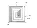
なお、本実施例の半導体装置の変形例によれば、図6に示すように、抵抗素子114のマイクロストリップをつづら折り状態以外の、渦巻状の抵抗素子114aにしてP型半導体基板PsubとP型ウェル領域PWLとの間にて配置することもできる。 According to a modification of the semiconductor device of the present embodiment, as shown in FIG. 6, the microstrip of the
100…半導体装置
102…保護対象回路
104…保護回路
111…RC直列回路
112…インバータ回路
113…保護用NMOSトランジスタ
114…抵抗素子
115…キャパシタ
118…PMOSトランジスタ
120…NMOSトランジスタ
VIA…ビア
VDD…電源ライン
VSS…グランドライン
CPG…コンタクトプラグ100 ...
Claims (5)
Translated fromJapanese前記基板上に形成され且つ絶縁膜で囲まれた抵抗素子が形成された第1導電型領域と、
前記抵抗素子の上面に接して積層形成された第2導電型領域と、
前記抵抗素子の上に層間絶縁層を介して形成されたキャパシタと、
前記抵抗素子の一端子および前記キャパシタの一端子を電気的に直列に接続するビアと、
前記抵抗素子の他端子および前記キャパシタの他端子のそれぞれに電気的に接続する電源ラインおよび接地ラインと、
を有することを特徴とする半導体装置。With the board
The first conductive type region in which the resistance element formed on the substrate and surrounded by the insulating film is formed,
The second conductive type region formed in contact with the upper surface of the resistance element and
Acapacitor formed on the resistance element via an interlayer insulating layer,
A via that electrically connects one terminal of the resistance element and one terminal of the capacitor in series,
A power supply line and a grounding line that are electrically connected to the other terminals of the resistance element and the other terminals of the capacitor, respectively.
A semiconductor device characterized by having.
Priority Applications (3)
| Application Number | Priority Date | Filing Date | Title |
|---|---|---|---|
| JP2018007919AJP7027176B2 (en) | 2018-01-22 | 2018-01-22 | Semiconductor device |
| CN201910057593.8ACN110071106B (en) | 2018-01-22 | 2019-01-22 | Semiconductor devices |
| US16/253,227US10930638B2 (en) | 2018-01-22 | 2019-01-22 | Semiconductor device having overlapping resistance element and capacitor |
Applications Claiming Priority (1)
| Application Number | Priority Date | Filing Date | Title |
|---|---|---|---|
| JP2018007919AJP7027176B2 (en) | 2018-01-22 | 2018-01-22 | Semiconductor device |
Publications (2)
| Publication Number | Publication Date |
|---|---|
| JP2019129171A JP2019129171A (en) | 2019-08-01 |
| JP7027176B2true JP7027176B2 (en) | 2022-03-01 |
Family
ID=67299324
Family Applications (1)
| Application Number | Title | Priority Date | Filing Date |
|---|---|---|---|
| JP2018007919AActiveJP7027176B2 (en) | 2018-01-22 | 2018-01-22 | Semiconductor device |
Country Status (3)
| Country | Link |
|---|---|
| US (1) | US10930638B2 (en) |
| JP (1) | JP7027176B2 (en) |
| CN (1) | CN110071106B (en) |
Families Citing this family (2)
| Publication number | Priority date | Publication date | Assignee | Title |
|---|---|---|---|---|
| WO2018227409A1 (en)* | 2017-06-14 | 2018-12-20 | 深圳市汇顶科技股份有限公司 | Mos field effect transistor-based filter circuit and chip |
| JP7507650B2 (en) | 2020-09-30 | 2024-06-28 | 三菱電機株式会社 | diode |
Citations (7)
| Publication number | Priority date | Publication date | Assignee | Title |
|---|---|---|---|---|
| JP2004111469A (en) | 2002-09-13 | 2004-04-08 | Oki Electric Ind Co Ltd | Semiconductor device |
| JP2007067096A (en) | 2005-08-30 | 2007-03-15 | Fujitsu Ltd | Semiconductor device |
| JP2008021962A (en) | 2006-06-12 | 2008-01-31 | Ricoh Co Ltd | Resistance element adjustment method, resistance element whose resistance value and temperature dependency characteristics are adjusted by the resistance element adjustment method, and current generator using the resistance element |
| JP2009135149A (en) | 2007-11-28 | 2009-06-18 | Panasonic Corp | Semiconductor integrated circuit |
| JP2012253241A (en) | 2011-06-03 | 2012-12-20 | Sony Corp | Semiconductor integrated circuit and manufacturing method of the same |
| JP2013120815A (en) | 2011-12-07 | 2013-06-17 | Sony Corp | Esd protecting circuit and semiconductor device including the same |
| JP2017123444A (en) | 2016-01-08 | 2017-07-13 | 株式会社デンソー | Semiconductor device |
Family Cites Families (33)
| Publication number | Priority date | Publication date | Assignee | Title |
|---|---|---|---|---|
| JPS57196558A (en)* | 1981-05-27 | 1982-12-02 | Nec Corp | Semiconductor integrated circuit device |
| US5994755A (en)* | 1991-10-30 | 1999-11-30 | Intersil Corporation | Analog-to-digital converter and method of fabrication |
| JP3095912B2 (en)* | 1992-12-24 | 2000-10-10 | 川崎製鉄株式会社 | Semiconductor integrated circuit device |
| US5583359A (en)* | 1995-03-03 | 1996-12-10 | Northern Telecom Limited | Capacitor structure for an integrated circuit |
| JPH10163429A (en)* | 1996-11-29 | 1998-06-19 | Mitsubishi Electric Corp | Semiconductor device |
| US6066537A (en)* | 1998-02-02 | 2000-05-23 | Tritech Microelectronics, Ltd. | Method for fabricating a shielded multilevel integrated circuit capacitor |
| JP3853513B2 (en)* | 1998-04-09 | 2006-12-06 | エルピーダメモリ株式会社 | Dynamic RAM |
| US6828638B2 (en)* | 1999-12-22 | 2004-12-07 | Intel Corporation | Decoupling capacitors for thin gate oxides |
| DE10144364A1 (en)* | 2001-09-10 | 2003-04-03 | Epcos Ag | Electrical multilayer component |
| WO2003052829A1 (en)* | 2001-12-14 | 2003-06-26 | Hitachi, Ltd. | Semiconductor device and method for manufacturing the same |
| JP2003332447A (en)* | 2002-05-13 | 2003-11-21 | Mitsubishi Electric Corp | Capacitive element |
| US7265433B2 (en)* | 2005-01-13 | 2007-09-04 | International Business Machines Corporation | On-pad broadband matching network |
| JP4800109B2 (en)* | 2005-09-13 | 2011-10-26 | ルネサスエレクトロニクス株式会社 | Semiconductor device |
| US7910450B2 (en)* | 2006-02-22 | 2011-03-22 | International Business Machines Corporation | Method of fabricating a precision buried resistor |
| JP5022643B2 (en)* | 2006-07-13 | 2012-09-12 | 株式会社東芝 | ESD protection circuit for semiconductor device |
| JP5314873B2 (en)* | 2007-10-05 | 2013-10-16 | ルネサスエレクトロニクス株式会社 | Semiconductor device |
| JP2010129893A (en)* | 2008-11-28 | 2010-06-10 | Sony Corp | Semiconductor integrated circuit |
| US9590027B2 (en)* | 2009-04-20 | 2017-03-07 | Nxp B.V. | Method for fabricating an integrated-passives device with a MIM capacitor and a high-accuracy resistor on top |
| US20110298432A1 (en)* | 2010-06-07 | 2011-12-08 | Skyworks Solutions, Inc | Apparatus and method for variable voltage function |
| US8368116B2 (en)* | 2010-06-09 | 2013-02-05 | Analog Devices, Inc. | Apparatus and method for protecting electronic circuits |
| CN103797572B (en)* | 2011-09-16 | 2016-06-22 | 富士电机株式会社 | High-voltage-resistant semiconductor device |
| US8624322B1 (en)* | 2012-07-17 | 2014-01-07 | Taiwan Semiconductor Manufacturing Company, Ltd. | High voltage device with a parallel resistor |
| US8963277B2 (en)* | 2013-03-13 | 2015-02-24 | Macronix International Co., Ltd. | Semiconductor structure and method of manufacturing the same |
| US9613968B2 (en)* | 2014-09-25 | 2017-04-04 | Kilopass Technology, Inc. | Cross-coupled thyristor SRAM semiconductor structures and methods of fabrication |
| JP2016111186A (en) | 2014-12-05 | 2016-06-20 | ソニー株式会社 | Semiconductor integrated circuit |
| US9825028B2 (en)* | 2015-01-07 | 2017-11-21 | Nxp B.V. | Ultra linear high voltage resistors |
| US9553139B2 (en)* | 2015-01-30 | 2017-01-24 | Semiconductor Components Industries, Llc | Semiconductor component and method of manufacture |
| US9484068B2 (en)* | 2015-02-17 | 2016-11-01 | Kilopass Technology, Inc. | MTP-thyristor memory cell circuits and methods of operation |
| US9673187B2 (en)* | 2015-04-07 | 2017-06-06 | Analog Devices, Inc. | High speed interface protection apparatus |
| JP2017045966A (en)* | 2015-08-28 | 2017-03-02 | ルネサスエレクトロニクス株式会社 | Semiconductor device |
| US9621033B2 (en)* | 2015-09-09 | 2017-04-11 | Nxp Usa, Inc. | Charge pump circuit for providing multiplied voltage |
| US10157907B2 (en)* | 2015-12-03 | 2018-12-18 | Taiwan Semiconductor Manufacturing Company, Ltd. | Semiconductor device and method of manufacturing the same |
| JP6690336B2 (en)* | 2016-03-18 | 2020-04-28 | 富士電機株式会社 | Semiconductor device |
- 2018
- 2018-01-22JPJP2018007919Apatent/JP7027176B2/enactiveActive
- 2019
- 2019-01-22CNCN201910057593.8Apatent/CN110071106B/enactiveActive
- 2019-01-22USUS16/253,227patent/US10930638B2/enactiveActive
Patent Citations (7)
| Publication number | Priority date | Publication date | Assignee | Title |
|---|---|---|---|---|
| JP2004111469A (en) | 2002-09-13 | 2004-04-08 | Oki Electric Ind Co Ltd | Semiconductor device |
| JP2007067096A (en) | 2005-08-30 | 2007-03-15 | Fujitsu Ltd | Semiconductor device |
| JP2008021962A (en) | 2006-06-12 | 2008-01-31 | Ricoh Co Ltd | Resistance element adjustment method, resistance element whose resistance value and temperature dependency characteristics are adjusted by the resistance element adjustment method, and current generator using the resistance element |
| JP2009135149A (en) | 2007-11-28 | 2009-06-18 | Panasonic Corp | Semiconductor integrated circuit |
| JP2012253241A (en) | 2011-06-03 | 2012-12-20 | Sony Corp | Semiconductor integrated circuit and manufacturing method of the same |
| JP2013120815A (en) | 2011-12-07 | 2013-06-17 | Sony Corp | Esd protecting circuit and semiconductor device including the same |
| JP2017123444A (en) | 2016-01-08 | 2017-07-13 | 株式会社デンソー | Semiconductor device |
Also Published As
| Publication number | Publication date |
|---|---|
| CN110071106A (en) | 2019-07-30 |
| US10930638B2 (en) | 2021-02-23 |
| US20190229107A1 (en) | 2019-07-25 |
| CN110071106B (en) | 2024-08-13 |
| JP2019129171A (en) | 2019-08-01 |
Similar Documents
| Publication | Publication Date | Title |
|---|---|---|
| JP5703790B2 (en) | Semiconductor device and manufacturing method thereof | |
| US6933551B1 (en) | Large value, compact, high yielding integrated circuit capacitors | |
| US5731614A (en) | Electrostatic protective device having elongate gate electrodes in a ladder structure | |
| JP2008091687A (en) | Semiconductor integrated circuit device | |
| JP7027176B2 (en) | Semiconductor device | |
| TW202105723A (en) | Transient voltage suppression device | |
| KR20020034909A (en) | Semiconductor integrated circuit system | |
| CN109300891A (en) | Electrostatic protection element and semiconductor device | |
| KR100297067B1 (en) | Semiconductor device and manufacturing method thereof | |
| JP5165321B2 (en) | Electrostatic breakdown protection element, electrostatic breakdown protection circuit, semiconductor device, and method of manufacturing semiconductor device | |
| TW201806124A (en) | Semiconductor electrostatic discharge protection circuit, semiconductor electrostatic discharge protection component and its layout structure | |
| JP7689428B2 (en) | Semiconductor Device | |
| JP3123489B2 (en) | Electrostatic protection circuit in semiconductor integrated circuit and method of manufacturing the same | |
| TW201816977A (en) | Electrostatic discharge protection element | |
| TWI728090B (en) | Semiconductor structure | |
| US7075156B1 (en) | Collector structure for electrostatic discharge protection circuits | |
| JP6656968B2 (en) | Semiconductor device having an ESD protection element | |
| KR200308025Y1 (en) | Layout of electrostatic discharge input protection circuit of semiconductor device | |
| KR950002204B1 (en) | Making method of diode for protecting circuit | |
| JP3017083B2 (en) | Input/Output Protection Circuit | |
| KR100384788B1 (en) | Input/output layout in a semiconductor device and structure thereof | |
| KR101050456B1 (en) | Static electricity protection device | |
| TW202510285A (en) | Electrostatic discharge protection device | |
| CN120035224A (en) | Semiconductor structure and method for forming the same | |
| JPH05267597A (en) | Mos transistor for input/output protective device |
Legal Events
| Date | Code | Title | Description |
|---|---|---|---|
| A621 | Written request for application examination | Free format text:JAPANESE INTERMEDIATE CODE: A621 Effective date:20201130 | |
| A977 | Report on retrieval | Free format text:JAPANESE INTERMEDIATE CODE: A971007 Effective date:20211020 | |
| A131 | Notification of reasons for refusal | Free format text:JAPANESE INTERMEDIATE CODE: A131 Effective date:20211026 | |
| A521 | Request for written amendment filed | Free format text:JAPANESE INTERMEDIATE CODE: A523 Effective date:20211222 | |
| TRDD | Decision of grant or rejection written | ||
| A01 | Written decision to grant a patent or to grant a registration (utility model) | Free format text:JAPANESE INTERMEDIATE CODE: A01 Effective date:20220118 | |
| A61 | First payment of annual fees (during grant procedure) | Free format text:JAPANESE INTERMEDIATE CODE: A61 Effective date:20220216 | |
| R150 | Certificate of patent or registration of utility model | Ref document number:7027176 Country of ref document:JP Free format text:JAPANESE INTERMEDIATE CODE: R150 |