JP7022794B2 - Optical system for displays - Google Patents
Optical system for displaysDownload PDFInfo
- Publication number
- JP7022794B2 JP7022794B2JP2020131863AJP2020131863AJP7022794B2JP 7022794 B2JP7022794 B2JP 7022794B2JP 2020131863 AJP2020131863 AJP 2020131863AJP 2020131863 AJP2020131863 AJP 2020131863AJP 7022794 B2JP7022794 B2JP 7022794B2
- Authority
- JP
- Japan
- Prior art keywords
- light
- coupler
- optical
- output coupler
- display
- Prior art date
- Legal status (The legal status is an assumption and is not a legal conclusion. Google has not performed a legal analysis and makes no representation as to the accuracy of the status listed.)
- Active
Links
- 230000003287optical effectEffects0.000titleclaimsdescription131
- 230000006870functionEffects0.000description7
- 239000011521glassSubstances0.000description5
- 230000003190augmentative effectEffects0.000description3
- 239000004973liquid crystal related substanceSubstances0.000description3
- 239000000463materialSubstances0.000description3
- 239000000758substrateSubstances0.000description3
- 108010010803GelatinProteins0.000description2
- 229920000159gelatinPolymers0.000description2
- 239000008273gelatinSubstances0.000description2
- 235000019322gelatineNutrition0.000description2
- 235000011852gelatine dessertsNutrition0.000description2
- 230000001902propagating effectEffects0.000description2
- 238000010586diagramMethods0.000description1
- SOCTUWSJJQCPFX-UHFFFAOYSA-Ndichromate(2-)Chemical compound[O-][Cr](=O)(=O)O[Cr]([O-])(=O)=OSOCTUWSJJQCPFX-UHFFFAOYSA-N0.000description1
- 230000005684electric fieldEffects0.000description1
- 210000003128headAnatomy0.000description1
- 239000005276holographic polymer dispersed liquid crystals (HPDLCs)Substances0.000description1
- 238000012986modificationMethods0.000description1
- 230000004048modificationEffects0.000description1
- 229920000642polymerPolymers0.000description1
- 229910052709silverInorganic materials0.000description1
- 239000004332silverSubstances0.000description1
- -1silver halideChemical class0.000description1
Images


Classifications
- G—PHYSICS
- G02—OPTICS
- G02B—OPTICAL ELEMENTS, SYSTEMS OR APPARATUS
- G02B27/00—Optical systems or apparatus not provided for by any of the groups G02B1/00 - G02B26/00, G02B30/00
- G02B27/01—Head-up displays
- G02B27/017—Head mounted
- G02B27/0172—Head mounted characterised by optical features
- G—PHYSICS
- G02—OPTICS
- G02B—OPTICAL ELEMENTS, SYSTEMS OR APPARATUS
- G02B27/00—Optical systems or apparatus not provided for by any of the groups G02B1/00 - G02B26/00, G02B30/00
- G02B27/01—Head-up displays
- G02B27/017—Head mounted
- G—PHYSICS
- G02—OPTICS
- G02B—OPTICAL ELEMENTS, SYSTEMS OR APPARATUS
- G02B6/00—Light guides; Structural details of arrangements comprising light guides and other optical elements, e.g. couplings
- G02B6/0001—Light guides; Structural details of arrangements comprising light guides and other optical elements, e.g. couplings specially adapted for lighting devices or systems
- G02B6/0011—Light guides; Structural details of arrangements comprising light guides and other optical elements, e.g. couplings specially adapted for lighting devices or systems the light guides being planar or of plate-like form
- G02B6/0013—Means for improving the coupling-in of light from the light source into the light guide
- G02B6/0023—Means for improving the coupling-in of light from the light source into the light guide provided by one optical element, or plurality thereof, placed between the light guide and the light source, or around the light source
- G—PHYSICS
- G02—OPTICS
- G02B—OPTICAL ELEMENTS, SYSTEMS OR APPARATUS
- G02B6/00—Light guides; Structural details of arrangements comprising light guides and other optical elements, e.g. couplings
- G02B6/0001—Light guides; Structural details of arrangements comprising light guides and other optical elements, e.g. couplings specially adapted for lighting devices or systems
- G02B6/0011—Light guides; Structural details of arrangements comprising light guides and other optical elements, e.g. couplings specially adapted for lighting devices or systems the light guides being planar or of plate-like form
- G02B6/0033—Means for improving the coupling-out of light from the light guide
- G02B6/0035—Means for improving the coupling-out of light from the light guide provided on the surface of the light guide or in the bulk of it
- G—PHYSICS
- G02—OPTICS
- G02B—OPTICAL ELEMENTS, SYSTEMS OR APPARATUS
- G02B27/00—Optical systems or apparatus not provided for by any of the groups G02B1/00 - G02B26/00, G02B30/00
- G02B27/01—Head-up displays
- G02B27/0101—Head-up displays characterised by optical features
- G02B2027/0123—Head-up displays characterised by optical features comprising devices increasing the field of view
- G—PHYSICS
- G02—OPTICS
- G02B—OPTICAL ELEMENTS, SYSTEMS OR APPARATUS
- G02B27/00—Optical systems or apparatus not provided for by any of the groups G02B1/00 - G02B26/00, G02B30/00
- G02B27/01—Head-up displays
- G02B27/017—Head mounted
- G02B27/0172—Head mounted characterised by optical features
- G02B2027/0174—Head mounted characterised by optical features holographic
- G—PHYSICS
- G02—OPTICS
- G02B—OPTICAL ELEMENTS, SYSTEMS OR APPARATUS
- G02B27/00—Optical systems or apparatus not provided for by any of the groups G02B1/00 - G02B26/00, G02B30/00
- G02B27/01—Head-up displays
- G02B27/017—Head mounted
- G02B2027/0178—Eyeglass type
Landscapes
- Physics & Mathematics (AREA)
- General Physics & Mathematics (AREA)
- Optics & Photonics (AREA)
- Diffracting Gratings Or Hologram Optical Elements (AREA)
- Eyeglasses (AREA)
- Optical Couplings Of Light Guides (AREA)
Description
Translated fromJapanese 本出願は、2017年6月6日に出願された国際出願PCT/US2017/036205号、及び2016年6月21日に出願された米国仮特許出願第62/352,754号の優先権を主張するものであり、本明細書において参照によりその全体が本明細書に組み込まれる。
本出願は、概して、光学システムに関し、より具体的には、ニアアイディスプレイ用の光学システムに関する。This application claims the priority of international application PCT / US2017 / 036205 filed on June 6, 2017, and US provisional patent application No. 62 / 352,754 filed on June 21, 2016. And is incorporated herein by reference in its entirety.
The present application generally relates to optical systems, and more specifically to optical systems for near-eye displays.
電子デバイスは、ユーザの目の近くに画像を表示するニアアイディスプレイを含むことができる。例えば、仮想現実ヘッドセット及び拡張現実ヘッドセットなどのデバイスは、ユーザがディスプレイを見ることを可能にする光学素子を有するニアアイディスプレイを含むことができる。 The electronic device can include a near-eye display that displays an image close to the user's eyes. For example, devices such as virtual reality headsets and augmented reality headsets can include near-eye displays with optical elements that allow the user to see the display.
そのようにデバイスを設計することは難しいことであり得る。注意が払われなければ、ニアアイディスプレイによって生成された視野の一部は、片方の目の位置から見えないことがあり得る。 Designing such a device can be difficult. If care is not taken, part of the field of view generated by the near-eye display may not be visible from the position of one eye.
ヘッドマウントデバイスなどの電子デバイスは、ユーザのために画像を生成する1つ以上のニアアイディスプレイを有することができる。ヘッドマウントデバイスは、仮想現実眼鏡であってもよく、又はビューアがビューアの周囲環境においてコンピュータ生成画像及び現実世界物体の両方を見ることを可能にする拡張現実ヘッドセットであってもよい。 An electronic device, such as a head-mounted device, can have one or more near-eye displays that produce images for the user. The head-mounted device may be virtual reality glasses or an augmented reality headset that allows the viewer to see both computer-generated images and real-world objects in the viewer's surroundings.
ニアアイディスプレイは、光を導くディスプレイユニット、及びディスプレイユニットからの光をユーザの目に向けて方向転換する光学システムを含むことができる。光学システムは、導波路に形成された入力カプラ及び出力カプラを含むことができる。入力カプラは、ディスプレイユニットディスプレイユニットからの光を、導波路において出力カプラに向かって伝搬するように、方向転換することができる。出力カプラは、入力カプラからの光を、ユーザの目に向かって導波路から出るように、方向転換することができる。入力カプラ及び出力カプラは、薄いホログラム、体積ホログラム、又は表面レリーフ格子などのホログラフィック光学素子から形成されてもよい。 The near-eye display can include a display unit that guides the light and an optical system that directs the light from the display unit toward the user's eyes. The optical system can include an input coupler and an output coupler formed in the waveguide. The input coupler can divert the light from the display unit display unit so that it propagates toward the output coupler in the waveguide. The output coupler can direct the light from the input coupler out of the waveguide towards the user's eyes. The input coupler and the output coupler may be formed from a holographic optical element such as a thin hologram, a volume hologram, or a surface relief grid.
光方向転換素子を使用して、方向転換されなければユーザの視野から外れる光をユーザの目に方向転換又は再分布させることができる。光方向転換素子は、ディスプレイユニットと入力カプラとの間に介在されてもよく、入力カプラと出力カプラとの間に介在されてもよく、又は出力カプラと一体化されてもよい。 An optical diversion element can be used to divert or redistribute light that would otherwise be out of the user's field of view into the user's eyes. The optical direction changing element may be interposed between the display unit and the input coupler, may be interposed between the input coupler and the output coupler, or may be integrated with the output coupler.
光方向転換素子がディスプレイユニットと入力カプラとの間に介在される構成では、光方向転換素子は、第2の導波路に二次入力カプラ及び二次出力カプラを含むことができる。 In a configuration in which the optical diversion element is interposed between the display unit and the input coupler, the optical diversion element may include a secondary input coupler and a secondary output coupler in the second waveguide.
光方向転換素子が入力カプラと出力カプラとの間に介在される構成では、光方向転換素子は、一次入力カプラ及び一次出力カプラと同じ導波路に二次入力カプラ及び二次出力カプラを含むことができる。他の構成では、光方向転換素子は、入力カプラと出力カプラとの間の1つのホログラフィック素子(例えば、入力カプラ及び出力カプラの両方として機能する)から形成されてもよい。 In a configuration in which the optical diversion element is interposed between the input coupler and the output coupler, the optical diversion element includes the secondary input coupler and the secondary output coupler in the same waveguide as the primary input coupler and the primary output coupler. Can be done. In other configurations, the optical diversion element may be formed from one holographic element between the input coupler and the output coupler (eg, acting as both an input coupler and an output coupler).
光方向転換素子が出力カプラと一体化(例えば、多重化)された構成では、光方向転換素子は、出力カプラの干渉パターンに非平行な1つ以上の干渉パターンを含むことができる。 In a configuration in which the optical diversion element is integrated (eg, multiplexed) with the output coupler, the optical diversion element can include one or more interference patterns that are non-parallel to the interference pattern of the output coupler.
1つ以上のニアアイディスプレイシステムを備えたデバイスを有する例示的なシステムを図1に示す。システム10は、支持構造12に取り付けられたニアアイディスプレイ20などの1つ以上のディスプレイを有するヘッドマウントデバイスであってもよい。支持構造12は、眼鏡の形状(例えば、支持フレーム)を有していてもよいし、ヘルメット形状を有する筐体を形成していてもよいし、若しくはユーザの頭部又は目の近くにニアアイディスプレイ20の構成要素を取り付けて固定するのに役立つ他の構成を有していてもよい。ニアアイディスプレイ20は、ディスプレイ20Aなどの1つ以上のディスプレイモジュール、及び光学システム20Bなどの1つ以上の光学システムを含むことができる。ディスプレイモジュール20Aは、支持構造12などの支持構造に取り付けられてもよい。ディスプレイモジュール20Aは、関連付けられた光学システム20Bを使用してユーザの目16に向けて方向転換された光を放射することができる。所望であれば、システム10は、各々がそれぞれのディスプレイモジュール20A及び光学システム20Bを有する2つのニアアイディスプレイ20(例えば、ユーザの目の各々に1つ)を含むことができる。 An exemplary system with a device with one or more near-eye display systems is shown in FIG. The
ディスプレイ20Aは、液晶ディスプレイ、有機発光ダイオードディスプレイ、又は他のタイプのディスプレイであってもよい。光学システム20Bは、ビューア(例えば、ビューアの目16)がディスプレイ20上の画像を見ることを可能にするレンズを形成することができる。左右それぞれの目16に関連付けられた(例えば、左側のレンズおよび右側のレンズを形成するための)2つの光学システム20Bがあってもよい。単一のディスプレイ20によって、片方又は両方の目16用の画像を生成することができるか、又は一対のディスプレイ20を使用して、目16用の画像を表示することができる。一例として、ディスプレイ20は、左側の光学システム20B及びビューアの左目に整列された左側のディスプレイモジュール20Aを含むことができ、また右側の光学システム20B及びビューアの右目に整列された右側のディスプレイモジュール20Aを含むことができる。複数のディスプレイを有する構成では、構成要素20Bによって形成されるレンズの焦点距離及び位置は、ディスプレイ間に存在する任意の隙間がユーザに見えないように(すなわち、左側のディスプレイの画像と右側のディスプレイの画像が重なるように又はシームレスに繋がるように)、選択され得る。 The
システム10が仮想現実眼鏡である構成では、ニアアイディスプレイ20は、ユーザの周囲環境のユーザの視野を遮る可能性がある。システム10が拡張現実眼鏡の構成である構成では、ディスプレイ20は透明であってもよい、及び/又はディスプレイ20にはハーフミラーなどの光ミキサを設けてもよく、それによってビューア16がディスプレイ20上の画像と、周囲環境の物体18などの外部物体とを同時に見ることを可能にする。 In a configuration where the
システム10は制御回路26を含むことができる。制御回路26は、マイクロプロセッサ、デジタルシグナルプロセッサ、マイクロコントローラ、ベースバンドプロセッサ、画像プロセッサ、処理回路を有する特定用途向け集積回路、及び/又は他の処理回路などの処理回路を含むことができ、またランダムアクセスメモリ、読み出し専用メモリ、フラッシュストレージ、ハードディスクストレージ、及び/又は他のストレージ(例えば、制御回路26において実行されるソフトウェアのためのコンピュータ命令を記憶するための非一時的なストレージ)を含むことができる。 The
システム10は、タッチセンサ、ボタン、音声入力及び他の入力を収集するためのマイクロフォン、センサ、並びに入力(例えば、ビューア16からのユーザ入力)を収集する他のデバイスなどの、入出力回路を含むことができ、また発光ダイオード、1つ以上のディスプレイ20、スピーカ、及び出力(例えば、ビューア16のための出力)を提供するための他のデバイスを含むことができる。システム10は、所望であれば、コンピュータ又は他の外部機器(例えば、ディスプレイ20に画像コンテンツを供給するコンピュータ)との通信をサポートするための無線回路及び/又は他の回路を含むことができる。所望であれば、加速度計、コンパス、周囲光センサ又は他の光検出器、近接センサ、走査レーザシステム、画像センサ、及び/又は他のセンサ、などのセンサを、ディスプレイ20の動作中に入力を収集する際に使用することができる。動作中、制御回路26は画像コンテンツをディスプレイ20に供給することができる。コンテンツは、(例えば、システム10に結合されたコンピュータ又は他のコンテンツソースから)遠隔受信されてもよく、及び/又は(例えば、テキスト、他のコンピュータ生成コンテンツ、などを)制御回路26によって生成されてもよい。制御回路26によってディスプレイ20に供給されるコンテンツを、ビューア16が見ることができる。 The
図2は、図1のシステム10において使用され得る例示的なニアアイディスプレイ20の上面図である。図2に示すように、ニアアイディスプレイ20は、ディスプレイモジュール20Aなどの1つ以上のディスプレイモジュール、及び光学システム20Bなどの光学システムを含むことができる。光学システム20Bは、導波路28、入力カプラ30、及び出力カプラ32などの光学素子を含むことができる。ディスプレイモジュール20Aは、ディスプレイユニット36及びコリメートレンズ34を含むことができる。所望であれば、ディスプレイモジュール20Aは、図1の支持構造12内に取り付けられてもよく、その一方で光学システム20Bは、(例えば、ユーザの目16と整列するレンズを形成するために)支持構造12の部品間に取り付けられてもよい。所望であれば、他の取り付け構成を使用してもよい。 FIG. 2 is a top view of an exemplary near-
ディスプレイユニット36は、液晶ディスプレイ、有機発光ダイオードディスプレイ、陰極線管、プラズマディスプレイ、プロジェクタディスプレイ(例えば、マイクロミラーアレイに基づくプロジェクタ)、反射型液晶ディスプレイ、又は他の適切なタイプのディスプレイに基づくディスプレイユニットであってもよい。ディスプレイ36は、ビューア16に表示される3次元コンテンツに関連付けられた光38を生成することができる。光38は、コリメートレンズ34などのレンズを使用してコリメートされてもよい。光学システム20Bを使用して、ディスプレイユニット36からビューア16に出力される光38を提供することができる。 The
光学システム20Bは、入力カプラ30及び出力カプラ32などの1つ以上のカプラを含むことができる。図2Aの例では、入力カプラ30及び出力カプラ32は、導波路28(例えば、ポリマー、ガラス、又は全反射を介して光を導くことができる他の透明基板)などの導波構造に少なくとも部分的に埋め込まれている。図2Bの例では、入力カプラ30及び出力カプラ32は、導波路28の外面に形成されている。 The
入力カプラ30は、ディスプレイユニット36からの光38を導波路28に結合するように構成され得るが、これに対し出力カプラ32は、導波路28内から、ユーザの目16に向けて導波路28の外部に光を結合するように構成され得る。例えば、ディスプレイ36は、光38をZ方向において光学システム20Bへと放射することができる。光38が入力カプラ30に入射すると、入力カプラ30は、光38が導波路28内で全反射によって(例えばX方向において)出力カプラ32に向かって伝搬するように、光38を方向転換することができる。光38が出力カプラ32に入射すると、出力カプラ32は、光38を、導波路28から出射させてビューアの目16に向けて(例えばZ軸に沿って戻して)方向転換することができる。 The
入力カプラ30及び出力カプラ32は、反射光学系及び屈折光学系に基づくものであってもよいし、ホログラフィック(例えば、回折)光学系に基づくものであってもよい。カプラ30及び32が反射光学系及び屈折光学系から形成される構成では、カプラ30及び32は、1つ以上の反射器(例えば、マイクロミラー又は他の反射器のアレイ)を含むことができる。カプラ30及び32がホログラフィック光学系に基づく構成では、カプラ30及び32は、フォトポリマーなどの体積ホログラフィック媒体、重クロム酸ゼラチンなどのゼラチン、ハロゲン化銀、ホログラフィックポリマー分散液晶、又は他の適切な体積ホログラフィック媒体など、を含むことができる。 The
ホログラフィック記録は、感光性光学材料内に光干渉パターン(例えば、屈折率が異なる領域が交互に現れる領域)として記憶され得る。光干渉パターンは、所与の光源で照明されると、光を回折させてホログラフィック記録の3次元再構成を生成する、ホログラフィック格子を生成することができる。回折格子は、永続的な干渉パターンでエンコードされた切り換え不可能な回折格子であってもよいし、ホログラフィック記録媒体に印加される電界を制御することによって回折光を変調することができる切り換え可能な回折格子であってもよい。 The holographic recording can be stored as an optical interference pattern (eg, a region in which regions having different refractive indexes appear alternately) in the photosensitive optical material. The optical interference pattern can generate a holographic grating that, when illuminated by a given light source, diffracts the light to produce a three-dimensional reconstruction of the holographic recording. The diffraction grating may be a non-switchable diffraction grating encoded by a permanent interference pattern, or the diffraction grating can be switched by controlling the electric field applied to the holographic recording medium. It may be a diffraction grating.
所望であれば、カプラ30及び32は、導波路28の厚さに比べて比較的大きな厚さを有することができる。例えば、カプラ30及び32の厚さT1は、500ミクロン~1000ミクロン、200ミクロン~800ミクロン、1000ミクロン超、又は他の適切な厚さであってもよく、これに対し導波路28の厚さT2は100ミクロン~500ミクロン、200ミクロン~300ミクロン、1mm~2mm、3mm未満、3mm超、又は他の適切な厚さであってもよい。図2Bに示すように、導波路28の表面にカプラ30及び32が形成された構成では、(例えば、図2Aに示したような導波路28に埋め込まれた構成とは異なり)、カプラ30及び32の厚さT1は、所望であれば、導波路28の厚さT2より大きくてもよい。しかし、これは単なる例示である。所望であれば、カプラ30及び32は比較的薄くてもよく(例えば50ミクロン)、導波路28は比較的厚くてもよい(例えば500ミクロン)。 If desired, the
カプラ30及び32に厚いフィルムを使用することは、出力画像の均一性を高めるのに役立つことができ、また異なる光学機能を記録するより多くの材料を提供することができる。例えば、より厚いカプラでは、異なる干渉パターンを記録するためにより多くの材料が利用可能である(例えば、第1の光学機能を有する第1の干渉パターンをカプラ内の1つの深さに記録することができ、第2の光学機能を有する第2の干渉パターンをカプラ内の別の深さに記録することができる、など)。例えば、カプラ30に記録された1つの光学機能は、所与の入力角度を有する光を第1の出力角度(例えば、45°)に方向転換することができ、これに対しカプラ30に記録された別の光学機能は、所与の入力角度を有する光を第2の出力角度(例えば、60°)に方向転換することができる。 The use of thick films for the
カプラ30及び32は、所望であれば、カラー3次元画像を形成するために多重ホログラム(例えば、赤-緑-青のホログラムなどの3色ホログラム)であってもよい。各カプラ30及び32における回折効率は、光が各カプラから円滑で均一なやり方で出射するように、変調されてもよい(例えば、カプラ30及び32の幅にわたって変更されてもよい)。例えば、回折効率は、光源からより遠いエリアに対してはより高くなってもよい(例えば、一例として、ディスプレイユニット36により近いカプラ30又は32の領域内の回折効率は10%であり得るが、その一方で一例として、ディスプレイユニット36からより遠いカプラ30又は32の領域内の回折効率は、70%であってもよい)。 The
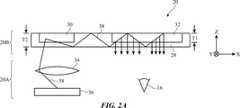
図3は、ニアアイディスプレイシステム20において使用され得る例示的な光学システム20Bの正面図である。図3に示すように、入力カプラ30は、出力カプラ32より幾分小さい。例えば、入力カプラ30は、約16mmの幅W1及び約32mmの長さL1を有してもよく、これに対し出力カプラ32は約37mmの幅W2及び約26mmの長さを有してもよい。入力カプラ30の中心と出力カプラ32の中心との間の距離Dは、約45mm又は他の適切な距離であってもよい。しかしながら、これらの寸法は単なる例示である。所望であれば、他の寸法を使用することができる(例えば、入力カプラ30は、出力カプラ32と同じか又はそれを超えるサイズであってもよい)。 FIG. 3 is a front view of an exemplary
図3に示すように、入力カプラ30は1つ以上の光干渉パターン40を有し、出力カプラ32は1つ以上の光干渉パターン42を有する。各光干渉パターンは、関連付けられた光学機能に従って入射光38を方向転換することができる。図3の例では、干渉パターン40及び42が、屈折率が交互に変化する垂直ストリップ(例えば、図3のY軸に平行なストリップ)から形成される。これは、入射光を所望の角度で方向転換する回折格子を形成する。 As shown in FIG. 3, the
図4及び図5は、図3に示したタイプの光学システム20Bが、ユーザの目16に向けて光をどのように方向転換することができるかを示す、例示的なニアアイディスプレイ20の側面図である。図4は、光が光学システム20Bにどのように入射されるかを示し、図5は、光が光学システム20Bをどのように出射されるかを示す。図4に示すように、ディスプレイユニット36は、光学システム20Bに向けて光38を放射することができる。コリメートレンズ34は、光38をコリメートして、光38を光学システム20Bに集束させることができる。コリメータ34からシステム20Bへ移動する光38は、X成分(X軸に平行)、Y成分(Y軸に平行)及びZ成分(Z軸に平行)を有するベクトルによって表され得る。 4 and 5 are aspects of an exemplary near-
入力カプラ30における干渉パターン40は、入射光38がX軸に沿って、導波路28において出力カプラ32に向かって伝搬するように、入射光38を方向転換することができる。出力カプラ32における干渉パターン42は、入射光38がX方向における伝搬を停止するが、その代わりに(図5に示すように)方向Zにおいて導波路28から出射するように、入射光38を方向転換することができる。 The
注意が払われなければ、光38の一部は、ビューアの目16の視野から外れることがあり得る。例えば、縁部光線38'などの一部の光線は、ユーザの目16に届かない可能性がある。これは、図3の垂直ストリップ干渉パターン40及び42によって、入射光38のX成分は(例えば、光38がX方向において出力カプラ32に向かって伝搬するように)変化するが、入射光38のY成分は変化しないためである。したがって、出力カプラ32の上部50T及び下部50Bから出力カプラ32を出射する光線38は、ユーザの視野の上又は下を通過する可能性がある。 If care is not taken, some of the light 38 may be out of the field of view of the viewer's
ユーザの視野から外れる光38の量を最少にするために、ニアアイディスプレイシステム20は、縁部光(例えば、図4の光38')を異なる位置に方向転換し、それによって縁部光がユーザの視野内にあるようにする光方向転換素子を含むことができる。図6及び図7は、光方向転換素子48が入力カプラ30の前に(例えば、ディスプレイ36と入力カプラ30との間に)配置されている例を示す。図8及び9は、光方向転換素子48が入力カプラ30と出力カプラ32との間に配置されている例を示し、図10~13は、光方向転換素子48が出力カプラ32と一体化されている例を示す。所望であれば、図1~図13に示す特徴の組み合わせをとる実施形態を使用することができる。例えば、光方向転換素子は、2つ以上の位置に配置されていてもよい(例えば、第1の光方向転換素子は入力カプラ30と出力カプラ32との間に配置されていてよく、第2の光方向転換素子は出力カプラ32と一体化されていてもよい)。 In order to minimize the amount of light 38 out of the user's field of view, the near-
光方向転換素子48は、所望であれば、カラー3次元画像を形成するための多重ホログラム(例えば、赤-緑-青ホログラムなどの3色ホログラム)を含むことができる。光方向転換素子48における回折効率は、光が光方向転換素子48から円滑で均一なやり方で出射するように、変調されてもよい(例えば、光方向転換素子48の幅にわたって変更されてもよい。例えば、回折効率は、光源からより遠いエリアに対しては高くなってもよい(例えば、ディスプレイユニット36により近い光方向転換素子48の領域内の回折効率は10%であり得るが、その一方で一例として、ディスプレイユニット36からより遠い光方向転換素子48の領域内の回折効率は、70%であってもよい)。 If desired, the optical
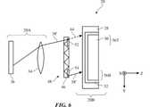
図6に示すように、光方向転換素子48は、導波路46などの導波路に形成された入力カプラ52及び出力カプラ54を含むことができる。光方向転換素子48は、光学システム20Bに取り付けられてもよく、又はディスプレイ20の他の構造に取り付けられてもよい。光方向転換素子48は、光学システム20Bと同様に動作することができる。例えば、カプラ52及び54は、所与の光学機能に従って入射光を方向転換するエンコードされた干渉パターンを有するホログラフィック光学素子であってもよい。しかし、光学システム20Bにおけるように、光をX方向に伝搬させるのではなく、光方向転換素子48を使用して、光をY方向に沿って(例えば、入力カプラ52から出力カプラ54へ)伝搬させることができる。 As shown in FIG. 6, the optical
例えば、入力カプラ52は、ディスプレイモジュール20Aからの縁部光38'が導波路46内でY方向において全反射によって、出力カプラ54に向かって伝搬するように、縁部光38'を方向転換する、1つ以上の干渉パターンを有することができる。出力カプラ54は、光38'を、光学システム20Bに向かって素子48から出射するように方向転換することができる。光38'は、(破線44で示すように)入力カプラ30の上部56Tに入射するのではなく、入力カプラ30の下部56Bに向かって放射される。したがって、図7に示すように、光38'が出力カプラ32から出射されると、光38'は、(矢印44によって示唆されているように、出力カプラ32の上部50Tから出射されるのではなく)ユーザの目16に向かって出力カプラ32の下部50Bから出射する。 For example, the
入力カプラ52及び出力カプラ54が導波路46に埋め込まれている図6の例は単なる例示に過ぎない。所望であれば、カプラ52及び54は、導波路46の外面に(例えば、両方ともディスプレイユニット36に面する導波路46の前面に、両方とも導波路28に面する導波路46の後面に、又は一方は導波路46の前面に及び他方は対向する導波路46の後面に)取り付けられてもよい。 The example of FIG. 6 in which the
図8の例では、光方向転換素子48は、入力カプラ30と出力カプラ32との間に介在されてもよい。図6の例のように、別個の導波路に取り付けられるのではなく、光方向転換素子48の入力カプラ52及び出力カプラ54は、入力カプラ30と出力カプラ32との間の導波路28上に、又は導波路28内に形成される。 In the example of FIG. 8, the optical
入力カプラ30は、縁部光38'がX方向において入力カプラ52に向かって伝搬するように、縁部光38'を方向転換することができる。入力カプラ52は、入力カプラ30からの縁部光38'が導波路28内でY方向において全反射によって、出力カプラ54に向かって伝搬するように、縁部光38'を方向転換する、1つ以上の干渉パターンを有することができる。出力カプラ54は、光38'がX方向において出力カプラ32に向かって伝搬するように、光38'を方向転換する、1つ以上の干渉パターンを有することができる。出力カプラ32は、(矢印44によって示唆されているように、出力カプラ32の上部50Tから出射されるのではなく)出力カプラ54からの光がユーザの目16に向かって導波路28から出射するように、光を方向転換することができる。 The
図9は、光方向転換素子48が入力カプラ30と出力カプラ32との間に介在された別の例を示す。この例では、光方向転換素子48は、出力カプラ32の長さL2よりも大きい長さL3を有するフィルムから形成される。光方向転換素子48は、Y軸に対して非平行である干渉パターン62を有する。干渉パターン62は、光38'がユーザの目16に導かれるように、光38'のY成分を方向転換するように構成され得る。例えば、図9に示すように、光方向転換要素48の上部48Tにおける干渉パターン62は、上部48Tに入射する縁部光38'のY成分を、Y方向で下方に、光方向転換要素48の下部48Bにおける干渉パターン62に向けて方向転換することができ、下部48Bにおける干渉パターン62は、続いて、縁部光38'のY成分を、出力カプラ32に向けて上方に方向転換することができる。同様に、光方向転換要素48の下部48Bにおける干渉パターン62は、下部48Bに入射する縁部38'のY成分を、Y方向で上方に、光方向転換要素48の上部48Tにおける干渉パターン62に向けて方向転換することができ、上部48Tにおける干渉パターン62は、続いて、縁部光38'のY成分を、出力カプラ32に向けて下方に方向転換することができる。出力カプラ32は、光方向転換素子48からの光を、ユーザの目16に向かって導波路28から出射するように方向転換することができる。 FIG. 9 shows another example in which the optical
図10の例では、1つ以上の光方向転換素子48を出力カプラ32に一体化することができる。図10の光方向転換素子48は、カプラ32においてエンコードされている光干渉パターンを含むことができる。したがって、カプラ32は、Y軸に平行な干渉パターン42の垂直ストリップだけでなく、Y軸に非平行な干渉パターン58も含む。干渉パターン58は、光38'がユーザの目16に導かれるように光38'のY成分を方向転換するように構成され得る。例えば、出力カプラ32の上部50Tにおける干渉パターン58は、上部50Tに入射する縁部光38'のY成分を、目線60に向けてY方向で下方に方向転換することができ、これに対し、出力カプラ32の下部50Bにおける干渉パターン58は、下部50bに入射する縁部光38'のY成分を、目線60に向けてY方向で上方に方向転換することができる。 In the example of FIG. 10, one or more optical
干渉パターン58が出力カプラ50の上部50T及び下部50Bにのみ配置されている図10の例は、単なる例示である。所望であれば、図11の例に示すように、干渉パターン58は、出力カプラ32の中央部分50Cにおいてエンコードされ得る。図12の例では、干渉パターン58は、出力カプラ32の中央部分50Cにおいてエンコードされ、かつX方向に沿ってサイズが(例えば、サイズP1からP2に)増大する。これは、光が出力カプラ32から、円滑で均一なやり方で回折されることを確実にするのに役立つ。図13の例では、干渉パターン58は、出力カプラ32全体にわたってエンコードされる。しかしながら、これらの例は単なる例示である。所望であれば、干渉パターン58は、他の適切な位置、サイズ、パターン、などで出力カプラ32にエンコードされ得る。光方向転換素子48が(例えば、Y軸に非平行な干渉パターンをエンコードすることによって)入力カプラ30と一体化された配置を使用することもできる。 The example of FIG. 10 in which the
一実施形態によれば、ディスプレイユニットと、ディスプレイユニットから光を受信し、光学システムから光が出射するように方向転換する光学システムであって、光学システムは、入力カプラ、出力カプラ、及び光を第1の方向に沿って伝搬させる第1の導波路を含む、光学システムと、ディスプレイユニットと光学システムとの間に介在された光方向転換素子であって、光方向転換素子は、光を第2の方向に沿って伝搬させる第2の導波路を含む、光方向転換素子と、を含む、ディスプレイシステムが提供される。 According to one embodiment, the display unit and an optical system that receives light from the display unit and changes its direction so that the light is emitted from the optical system, wherein the optical system has an input coupler, an output coupler, and light. An optical direction-changing element interposed between an optical system and a display unit and an optical system, comprising a first waveguide that propagates along a first direction, wherein the light-directing element directs light. A display system is provided that includes an optical diversion element that includes a second waveguide that propagates along two directions.
別の実施形態によれば、入力カプラ及び出力カプラの各々は、ホログラフィック光学素子を含む。 According to another embodiment, each of the input coupler and the output coupler comprises a holographic optical element.
別の実施形態によれば、入力カプラは、光方向転換要素から光を受信し、その光を出力カプラに向けて方向転換する。 According to another embodiment, the input coupler receives light from an optical diversion element and directs the light towards the output coupler.
別の実施形態によれば、出力カプラは、入力カプラから光を受信し、その光を光学システムから出射するように方向転換する。 According to another embodiment, the output coupler receives light from the input coupler and redirects the light out of the optical system.
別の実施形態によれば、光方向転換素子は、第2の導波路に付加的な入力カプラ及び付加的な出力カプラを含む。 According to another embodiment, the optical diversion element includes an additional input coupler and an additional output coupler in the second waveguide.
別の実施形態によれば、付加的な入力カプラ及び付加的な出力カプラの各々は、ホログラフィック光学素子を含む。 According to another embodiment, each of the additional input coupler and the additional output coupler comprises a holographic optical element.
別の実施形態によれば、付加的な入力カプラは、ディスプレイユニットから光を受信し、その光を付加的な出力カプラに向けて方向転換する。 According to another embodiment, the additional input coupler receives light from the display unit and directs the light towards the additional output coupler.
別の実施形態によれば、付加的な出力カプラは、付加的な入力カプラから光を受信し、その光を入力カプラに向けて方向転換する。 According to another embodiment, the additional output coupler receives light from the additional input coupler and redirects the light towards the input coupler.
別の実施形態によれば、第1の方向は第2の方向に対して垂直である。 According to another embodiment, the first direction is perpendicular to the second direction.
一実施形態によれば、ディスプレイユニットと、ディスプレイユニットから光を受信し、光学システムから光が出射するように方向転換する光学システムであって、光学システムは、第1の入力カプラ、第1の出力カプラ、及び導波路を含む、光学システムと、入力カプラと出力カプラとの間に介在された光方向転換素子であって、光方向転換素子は、導波路に第2の入力カプラ及び第2の出力カプラを含み、第2の入力カプラは光を第1の入力カプラから受信し、第1の出力カプラは光を第2の出力カプラから受信する、光方向転換素子と、を含むディスプレイシステムが提供される。 According to one embodiment, the display unit and an optical system that receives light from the display unit and changes the direction so that light is emitted from the optical system, wherein the optical system is a first input coupler, a first. An optical diversion element interposed between an optical system including an output coupler and a waveguide and an input coupler and an output coupler, the optical diversion element is a second input coupler and a second input coupler in the waveguide. A display system comprising an optical directing element, the second input coupler receiving light from a first input coupler and the first output coupler receiving light from a second output coupler. Is provided.
別の実施形態によれば、第1の入力カプラ、第2の入力カプラ、第1の出力カプラ及び第2の出力カプラの各々は、ホログラフィック光学素子を含む。 According to another embodiment, each of the first input coupler, the second input coupler, the first output coupler and the second output coupler includes a holographic optical element.
別の実施形態によれば、導波路は、第1の入力カプラから第2の入力カプラへ第1の方向に沿って光を伝搬させ、導波路は、第2の入力カプラから第2の出力カプラへ第2の方向に沿って光を伝搬させる。 According to another embodiment, the waveguide propagates light from the first input coupler to the second input coupler along the first direction, and the waveguide is from the second input coupler to the second output. Propagate light to the coupler along the second direction.
別の実施形態によれば、第1の方向は第2の方向に対して垂直である。 According to another embodiment, the first direction is perpendicular to the second direction.
別の実施形態によれば、第1の入力カプラは、第1の出力カプラよりも小さい寸法を有する。 According to another embodiment, the first input coupler has smaller dimensions than the first output coupler.
一実施形態によれば、ディスプレイユニットと、
ディスプレイユニットから光を受信し、光学システムから光が出射するように方向転換する光学システムであって、光学システムは、入力カプラ、出力カプラ、及び入力カプラから出力カプラに光を伝搬させる導波路を含み、出力カプラは、第1の非平行な干渉パターン及び第2の非平行な干渉パターンを含む、光学システムと、を含むディスプレイシステムが提供される。According to one embodiment, the display unit and
An optical system that receives light from a display unit and redirects it to emit light from the optical system, where the optical system provides an input coupler, an output coupler, and a waveguide that propagates the light from the input coupler to the output coupler. The output coupler includes an optical system, including a first non-parallel interference pattern and a second non-parallel interference pattern, and a display system including.
別の実施形態によれば、入力カプラ及び出力カプラの厚さは、導波路の厚さよりも大きい。 According to another embodiment, the thickness of the input coupler and the output coupler is larger than the thickness of the waveguide.
別の実施形態によれば、入力カプラ及び出力カプラの各々は、ホログラフィック光学素子を含む。 According to another embodiment, each of the input coupler and the output coupler comprises a holographic optical element.
別の実施形態によれば、ホログラフィック光学素子は色多重化される。 According to another embodiment, the holographic optics are color multiplexed.
別の実施形態によれば、第1及び第2の干渉パターンの各々は、変調された回折効率を有する。 According to another embodiment, each of the first and second interference patterns has a modulated diffraction efficiency.
別の実施形態によれば、第2の干渉パターンは、出力カプラの上部及び出力カプラの下部に配置される。 According to another embodiment, the second interference pattern is located above the output coupler and below the output coupler.
前述は単なる例示に過ぎず、記載された実施形態に対して様々な修正を行うことができる。前述の実施形態は、個別に又は任意の組み合わせで実装され得る。 The above is merely an example, and various modifications can be made to the described embodiments. The aforementioned embodiments may be implemented individually or in any combination.
Claims (5)
Translated fromJapaneseヘッドマウント支持構造と、
前記ヘッドマウント支持構造に結合されたディスプレイユニットと、
前記ディスプレイユニットから光を受信し、光学システムから前記光が出射するように方向転換する前記光学システムであって、前記光学システムは、入力カプラ、出力カプラ、及び前記入力カプラから前記出力カプラに光を伝搬させる導波路を含み、前記出力カプラは、互いに非平行な第1及び第2の干渉パターンを含む、前記光学システムと、
を備え、
前記入力カプラ及び前記出力カプラの厚さは、前記導波路の厚さよりも大きい、ディスプレイシステム。It ’s a display system.
Head mount support structure and
A display unit coupled to the head mount support structure and
The optical system that receives light from the display unit and redirects the light so that it is emitted from the optical system, wherein the optical system emits light from an input coupler, an output coupler, and an input coupler to the output coupler. The optical system comprises a waveguide that propagates the light, and the output coupler contains first and second interference patterns that are non-parallel toeach other .
Equipped with
A display systemin which the thickness of the input coupler and the output coupler is greater than the thickness of the waveguide .
Applications Claiming Priority (2)
| Application Number | Priority Date | Filing Date | Title |
|---|---|---|---|
| US201662352754P | 2016-06-21 | 2016-06-21 | |
| US62/352,754 | 2016-06-21 |
Related Parent Applications (1)
| Application Number | Title | Priority Date | Filing Date |
|---|---|---|---|
| JP2018549529ADivisionJP7065783B2 (en) | 2016-06-21 | 2017-06-06 | Optical system for displays |
Publications (2)
| Publication Number | Publication Date |
|---|---|
| JP2020201496A JP2020201496A (en) | 2020-12-17 |
| JP7022794B2true JP7022794B2 (en) | 2022-02-18 |
Family
ID=59071116
Family Applications (2)
| Application Number | Title | Priority Date | Filing Date |
|---|---|---|---|
| JP2018549529AActiveJP7065783B2 (en) | 2016-06-21 | 2017-06-06 | Optical system for displays |
| JP2020131863AActiveJP7022794B2 (en) | 2016-06-21 | 2020-08-03 | Optical system for displays |
Family Applications Before (1)
| Application Number | Title | Priority Date | Filing Date |
|---|---|---|---|
| JP2018549529AActiveJP7065783B2 (en) | 2016-06-21 | 2017-06-06 | Optical system for displays |
Country Status (6)
| Country | Link |
|---|---|
| US (2) | US12019238B2 (en) |
| EP (2) | EP4451042A3 (en) |
| JP (2) | JP7065783B2 (en) |
| KR (1) | KR102128673B1 (en) |
| CN (2) | CN109416470A (en) |
| WO (1) | WO2017222808A1 (en) |
Families Citing this family (23)
| Publication number | Priority date | Publication date | Assignee | Title |
|---|---|---|---|---|
| JP7166927B2 (en) | 2016-06-20 | 2022-11-08 | アコニア ホログラフィックス、エルエルシー | pupil dilation |
| US11054581B2 (en) | 2017-03-01 | 2021-07-06 | Akonia Holographics Llc | Ducted pupil expansion |
| IL278511B2 (en)* | 2018-05-17 | 2025-01-01 | Lumus Ltd | Near-eye display having overlapping projector assemblies |
| WO2020023546A1 (en)* | 2018-07-24 | 2020-01-30 | Magic Leap, Inc. | Diffractive optical elements with mitigation of rebounce-induced light loss and related systems and methods |
| US11822079B2 (en)* | 2018-08-10 | 2023-11-21 | Apple Inc. | Waveguided display system with adjustable lenses |
| US12147038B2 (en) | 2018-09-24 | 2024-11-19 | Apple Inc. | Optical systems with interleaved light redirectors |
| JP2020064096A (en)* | 2018-10-15 | 2020-04-23 | ソニー株式会社 | Image display device, head mounted display, manufacturing method of image display device and adjustment method of image display device |
| JP7100567B2 (en)* | 2018-11-14 | 2022-07-13 | 株式会社日立エルジーデータストレージ | Light guide plate and image display device |
| KR102172612B1 (en)* | 2018-11-22 | 2020-11-02 | 한국전자기술연구원 | Method for Generating Eye-Boxes with Wide Vertical Field of View in Lightguide based Image Providing Apparatus |
| US11740460B2 (en) | 2018-11-29 | 2023-08-29 | Apple Inc. | Optical systems with multi-layer holographic combiners |
| DE102019102614A1 (en) | 2019-02-01 | 2020-08-06 | Carl Zeiss Jena Gmbh | Screen with a transparent base |
| DE102019102607A1 (en)* | 2019-02-01 | 2020-08-06 | Carl Zeiss Jena Gmbh | Functionalized waveguide for a detector system |
| DE102019102609A1 (en)* | 2019-02-01 | 2020-08-06 | Carl Zeiss Jena Gmbh | Functionalized waveguide for a detector system and a lighting and / or projection system |
| DE102019102606A1 (en)* | 2019-02-01 | 2020-08-06 | Carl Zeiss Jena Gmbh | Functionalized waveguide for a detector system |
| DE102019102608A1 (en) | 2019-02-01 | 2020-08-06 | Carl Zeiss Jena Gmbh | Functionalized waveguide for a detector system |
| DE102019102604A1 (en) | 2019-02-01 | 2020-08-06 | Carl Zeiss Jena Gmbh | Functionalized waveguide for a detector system |
| US12055721B2 (en) | 2019-03-20 | 2024-08-06 | Magic Leap, Inc. | System for collecting light |
| TWI756691B (en)* | 2019-05-30 | 2022-03-01 | 美商蘋果公司 | Optical system, head-mounted device, and display system |
| US20210055551A1 (en)* | 2019-08-23 | 2021-02-25 | Facebook Technologies, Llc | Dispersion compensation in volume bragg grating-based waveguide display |
| KR102151883B1 (en)* | 2019-09-27 | 2020-09-03 | 한국전자기술연구원 | Crosstalk Reduction Method by Adjusting Pixel Radiation Angle in Waveguide Display for Finite Depth Image |
| CN115349105A (en)* | 2020-03-31 | 2022-11-15 | 索尼集团公司 | Optical device, method for manufacturing optical device, and image display device |
| WO2022159716A1 (en)* | 2021-01-22 | 2022-07-28 | Vuzix Corporation | Image light guide with compound in-coupling diffractive optic |
| US12118951B2 (en)* | 2022-08-17 | 2024-10-15 | Ii-Vi Delaware, Inc. | Display system with optical device |
Citations (3)
| Publication number | Priority date | Publication date | Assignee | Title |
|---|---|---|---|---|
| JP2010282231A (en) | 2004-03-29 | 2010-12-16 | Sony Corp | Image display device |
| US20130314793A1 (en) | 2012-05-22 | 2013-11-28 | Steven John Robbins | Waveguide optics focus elements |
| JP2016085430A (en) | 2014-10-29 | 2016-05-19 | セイコーエプソン株式会社 | Virtual image display device |
Family Cites Families (18)
| Publication number | Priority date | Publication date | Assignee | Title |
|---|---|---|---|---|
| EP1068548B1 (en) | 1998-04-02 | 2003-11-12 | Elop Electro-Optics Industries Ltd. | Holographic optical devices |
| US20060132914A1 (en)* | 2003-06-10 | 2006-06-22 | Victor Weiss | Method and system for displaying an informative image against a background image |
| US7206107B2 (en)* | 2004-12-13 | 2007-04-17 | Nokia Corporation | Method and system for beam expansion in a display device |
| EP1943556B1 (en)* | 2005-11-03 | 2009-02-11 | Mirage Innovations Ltd. | Binocular optical relay device |
| JP2007219106A (en)* | 2006-02-16 | 2007-08-30 | Konica Minolta Holdings Inc | Optical device for expanding diameter of luminous flux, video display device and head mount display |
| EP3667399A1 (en)* | 2007-06-04 | 2020-06-17 | Magic Leap, Inc. | A diffractive beam expander |
| US20100302644A1 (en)* | 2007-09-18 | 2010-12-02 | Mirage Innovations Ltd | Slanted optical device |
| US8233204B1 (en)* | 2009-09-30 | 2012-07-31 | Rockwell Collins, Inc. | Optical displays |
| JP5494153B2 (en) | 2010-04-08 | 2014-05-14 | ソニー株式会社 | Image display method for head mounted display |
| EP3309602A1 (en) | 2011-08-29 | 2018-04-18 | Vuzix Corporation | Controllable waveguide for near-eye display applications |
| US8736963B2 (en) | 2012-03-21 | 2014-05-27 | Microsoft Corporation | Two-dimensional exit-pupil expansion |
| US9671566B2 (en)* | 2012-06-11 | 2017-06-06 | Magic Leap, Inc. | Planar waveguide apparatus with diffraction element(s) and system employing same |
| KR20140077378A (en) | 2012-12-14 | 2014-06-24 | 한국전자통신연구원 | Apparatus for head mounted display using holographic optical element lens |
| WO2014109115A1 (en) | 2013-01-10 | 2014-07-17 | ソニー株式会社 | Image display device, image generating device, and transparent spatial light modulating device |
| US9164290B2 (en)* | 2013-11-06 | 2015-10-20 | Microsoft Corporation | Grating configurations for a tiled waveguide display |
| JP6287131B2 (en) | 2013-12-02 | 2018-03-07 | セイコーエプソン株式会社 | Virtual image display device |
| US10317679B2 (en)* | 2016-04-04 | 2019-06-11 | Akonia Holographics, Llc | Light homogenization |
| US10353202B2 (en)* | 2016-06-09 | 2019-07-16 | Microsoft Technology Licensing, Llc | Wrapped waveguide with large field of view |
- 2017
- 2017-06-06EPEP24192363.0Apatent/EP4451042A3/enactivePending
- 2017-06-06KRKR1020187027391Apatent/KR102128673B1/enactiveActive
- 2017-06-06WOPCT/US2017/036205patent/WO2017222808A1/ennot_activeCeased
- 2017-06-06USUS16/089,006patent/US12019238B2/enactiveActive
- 2017-06-06CNCN201780020762.XApatent/CN109416470A/enactivePending
- 2017-06-06CNCN202410999864.2Apatent/CN118671976A/enactivePending
- 2017-06-06JPJP2018549529Apatent/JP7065783B2/enactiveActive
- 2017-06-06EPEP17731027.3Apatent/EP3420395A1/ennot_activeWithdrawn
- 2020
- 2020-08-03JPJP2020131863Apatent/JP7022794B2/enactiveActive
- 2024
- 2024-05-21USUS18/670,007patent/US20240302664A1/enactivePending
Patent Citations (3)
| Publication number | Priority date | Publication date | Assignee | Title |
|---|---|---|---|---|
| JP2010282231A (en) | 2004-03-29 | 2010-12-16 | Sony Corp | Image display device |
| US20130314793A1 (en) | 2012-05-22 | 2013-11-28 | Steven John Robbins | Waveguide optics focus elements |
| JP2016085430A (en) | 2014-10-29 | 2016-05-19 | セイコーエプソン株式会社 | Virtual image display device |
Also Published As
| Publication number | Publication date |
|---|---|
| CN109416470A (en) | 2019-03-01 |
| JP7065783B2 (en) | 2022-05-12 |
| EP4451042A3 (en) | 2025-03-26 |
| EP4451042A2 (en) | 2024-10-23 |
| EP3420395A1 (en) | 2019-01-02 |
| JP2019517014A (en) | 2019-06-20 |
| CN118671976A (en) | 2024-09-20 |
| US20240302664A1 (en) | 2024-09-12 |
| JP2020201496A (en) | 2020-12-17 |
| KR102128673B1 (en) | 2020-06-30 |
| US20190377181A1 (en) | 2019-12-12 |
| KR20180115311A (en) | 2018-10-22 |
| US12019238B2 (en) | 2024-06-25 |
| WO2017222808A1 (en) | 2017-12-28 |
Similar Documents
| Publication | Publication Date | Title |
|---|---|---|
| JP7022794B2 (en) | Optical system for displays | |
| CN114026485B (en) | Optical system with reflective prism input coupler | |
| CN113966482B (en) | Display system with multiple light paths for performing concave | |
| CN103135234B (en) | Beam-expanding device, image display and optical device | |
| CN115066643B (en) | Optical system with angle selective transmission filter | |
| US12298506B2 (en) | Optical systems with low resolution peripheral displays | |
| US20250053016A1 (en) | Optical Systems with Interleaved Light Redirectors | |
| JP2024531524A (en) | Optical system for directing display module light to a waveguide - Patents.com | |
| US20230314796A1 (en) | Optical Systems Having Edge-Coupled Media Layers | |
| US12216282B2 (en) | Waveguide display with gaze tracking | |
| US20250271681A1 (en) | Display with Collimating Optics Including an Annular Mirror | |
| US20250291164A1 (en) | Display with a Catadioptric Collimating Lens | |
| US20220004005A1 (en) | Optical Systems for Providing Field Angle Dependent Pupil Sizes Within a Waveguide |
Legal Events
| Date | Code | Title | Description |
|---|---|---|---|
| A521 | Request for written amendment filed | Free format text:JAPANESE INTERMEDIATE CODE: A523 Effective date:20200826 | |
| A621 | Written request for application examination | Free format text:JAPANESE INTERMEDIATE CODE: A621 Effective date:20200826 | |
| RD03 | Notification of appointment of power of attorney | Free format text:JAPANESE INTERMEDIATE CODE: A7423 Effective date:20201203 | |
| RD04 | Notification of resignation of power of attorney | Free format text:JAPANESE INTERMEDIATE CODE: A7424 Effective date:20210210 | |
| A977 | Report on retrieval | Free format text:JAPANESE INTERMEDIATE CODE: A971007 Effective date:20210601 | |
| A131 | Notification of reasons for refusal | Free format text:JAPANESE INTERMEDIATE CODE: A131 Effective date:20210614 | |
| A521 | Request for written amendment filed | Free format text:JAPANESE INTERMEDIATE CODE: A523 Effective date:20210831 | |
| TRDD | Decision of grant or rejection written | ||
| A01 | Written decision to grant a patent or to grant a registration (utility model) | Free format text:JAPANESE INTERMEDIATE CODE: A01 Effective date:20220106 | |
| A61 | First payment of annual fees (during grant procedure) | Free format text:JAPANESE INTERMEDIATE CODE: A61 Effective date:20220207 | |
| R150 | Certificate of patent or registration of utility model | Ref document number:7022794 Country of ref document:JP Free format text:JAPANESE INTERMEDIATE CODE: R150 | |
| R250 | Receipt of annual fees | Free format text:JAPANESE INTERMEDIATE CODE: R250 |